TMS320F2810, TMS320F2811, TMS320F2812 TMS320C2810, TMS320C2811, TMS320C2812 Digital Signal Processors Data Manual PRODUCTION DATA information is current as of publication date. Products conform to specifications per the terms of the Texas Instruments standard warranty. Production processing does not necessarily include testing of all parameters. Literature Number: SPRS174T April 2001– Revised May 2012

Welcome message from author
This document is posted to help you gain knowledge. Please leave a comment to let me know what you think about it! Share it to your friends and learn new things together.
Transcript

TMS320F2810, TMS320F2811, TMS320F2812TMS320C2810, TMS320C2811, TMS320C2812Digital Signal Processors
Data Manual
PRODUCTION DATA information is current as of publication date.Products conform to specifications per the terms of the TexasInstruments standard warranty. Production processing does notnecessarily include testing of all parameters.
Literature Number: SPRS174T
April 2001–Revised May 2012

TMS320F2810, TMS320F2811, TMS320F2812TMS320C2810, TMS320C2811, TMS320C2812
www.ti.com SPRS174T –APRIL 2001–REVISED MAY 2012
Contents1 TMS320F281x, TMS320C281x DSPs ..................................................................................... 10
1.1 Features .................................................................................................................... 101.2 Getting Started ............................................................................................................. 11
2 Introduction ...................................................................................................................... 122.1 Description ................................................................................................................. 122.2 Device Summary .......................................................................................................... 132.3 Pin Assignments ........................................................................................................... 14
2.3.1 Terminal Assignments for the GHH/ZHH Packages ....................................................... 142.3.2 Pin Assignments for the PGF Package ...................................................................... 152.3.3 Pin Assignments for the PBK Package ...................................................................... 16
2.4 Signal Descriptions ........................................................................................................ 173 Functional Overview .......................................................................................................... 26
3.1 Memory Map ............................................................................................................... 273.2 Brief Descriptions .......................................................................................................... 32
3.2.1 C28x CPU ....................................................................................................... 323.2.2 Memory Bus (Harvard Bus Architecture) .................................................................... 323.2.3 Peripheral Bus .................................................................................................. 323.2.4 Real-Time JTAG and Analysis ................................................................................ 333.2.5 External Interface (XINTF) (2812 Only) ...................................................................... 333.2.6 Flash (F281x Only) ............................................................................................. 333.2.7 ROM (C281x Only) ............................................................................................. 333.2.8 M0, M1 SARAMs ............................................................................................... 343.2.9 L0, L1, H0 SARAMs ............................................................................................ 343.2.10 Boot ROM ....................................................................................................... 343.2.11 Security .......................................................................................................... 343.2.12 Peripheral Interrupt Expansion (PIE) Block ................................................................. 363.2.13 External Interrupts (XINT1, XINT2, XINT13, XNMI) ........................................................ 363.2.14 Oscillator and PLL .............................................................................................. 363.2.15 Watchdog ........................................................................................................ 363.2.16 Peripheral Clocking ............................................................................................. 363.2.17 Low-Power Modes .............................................................................................. 363.2.18 Peripheral Frames 0, 1, 2 (PFn) .............................................................................. 373.2.19 General-Purpose Input/Output (GPIO) Multiplexer ......................................................... 373.2.20 32-Bit CPU-Timers (0, 1, 2) ................................................................................... 373.2.21 Control Peripherals ............................................................................................. 373.2.22 Serial Port Peripherals ......................................................................................... 38
3.3 Register Map ............................................................................................................... 393.4 Device Emulation Registers .............................................................................................. 413.5 External Interface, XINTF (2812 Only) ................................................................................. 42
3.5.1 Timing Registers ................................................................................................ 433.5.2 XREVISION Register ........................................................................................... 43
3.6 Interrupts .................................................................................................................... 443.6.1 External Interrupts .............................................................................................. 47
3.7 System Control ............................................................................................................ 483.8 OSC and PLL Block ....................................................................................................... 50
3.8.1 Loss of Input Clock ............................................................................................. 513.9 PLL-Based Clock Module ................................................................................................ 523.10 External Reference Oscillator Clock Option ........................................................................... 523.11 Watchdog Block ........................................................................................................... 533.12 Low-Power Modes Block ................................................................................................. 54
4 Peripherals ....................................................................................................................... 55
2 Contents Copyright © 2001–2012, Texas Instruments Incorporated

TMS320F2810, TMS320F2811, TMS320F2812TMS320C2810, TMS320C2811, TMS320C2812
www.ti.com SPRS174T –APRIL 2001–REVISED MAY 2012
4.1 32-Bit CPU-Timers 0/1/2 ................................................................................................. 554.2 Event Manager Modules (EVA, EVB) ................................................................................... 58
4.2.1 General-Purpose (GP) Timers ................................................................................ 614.2.2 Full-Compare Units ............................................................................................. 614.2.3 Programmable Deadband Generator ........................................................................ 614.2.4 PWM Waveform Generation .................................................................................. 614.2.5 Double Update PWM Mode ................................................................................... 614.2.6 PWM Characteristics ........................................................................................... 624.2.7 Capture Unit ..................................................................................................... 624.2.8 Quadrature-Encoder Pulse (QEP) Circuit ................................................................... 624.2.9 External ADC Start-of-Conversion ........................................................................... 62
4.3 Enhanced Analog-to-Digital Converter (ADC) Module ............................................................... 634.4 Enhanced Controller Area Network (eCAN) Module .................................................................. 684.5 Multichannel Buffered Serial Port (McBSP) Module .................................................................. 734.6 Serial Communications Interface (SCI) Module ....................................................................... 774.7 Serial Peripheral Interface (SPI) Module ............................................................................... 804.8 GPIO MUX ................................................................................................................. 83
5 Development Support ........................................................................................................ 865.1 Device and Development Support Tool Nomenclature ............................................................... 865.2 Documentation Support .................................................................................................. 875.3 Community Resources .................................................................................................... 89
6 Electrical Specifications ..................................................................................................... 916.1 Absolute Maximum Ratings .............................................................................................. 916.2 Recommended Operating Conditions .................................................................................. 916.3 Electrical Characteristics Over Recommended Operating Conditions (Unless Otherwise Noted) ............. 926.4 Current Consumption ..................................................................................................... 936.5 Current Consumption Graphs ............................................................................................ 956.6 Reducing Current Consumption ......................................................................................... 976.7 Emulator Connection Without Signal Buffering for the DSP ......................................................... 976.8 Power Sequencing Requirements ....................................................................................... 986.9 Signal Transition Levels ................................................................................................. 1006.10 Timing Parameter Symbology .......................................................................................... 1016.11 General Notes on Timing Parameters ................................................................................ 1016.12 Test Load Circuit ......................................................................................................... 1016.13 Device Clock Table ...................................................................................................... 1026.14 Clock Requirements and Characteristics ............................................................................. 103
6.14.1 Input Clock Requirements ................................................................................... 1036.14.2 Output Clock Characteristics ................................................................................ 104
6.15 Reset Timing ............................................................................................................. 1046.16 Low-Power Mode Wakeup Timing ..................................................................................... 1086.17 Event Manager Interface ................................................................................................ 112
6.17.1 PWM Timing ................................................................................................... 1126.17.2 Interrupt Timing ................................................................................................ 114
6.18 General-Purpose Input/Output (GPIO) – Output Timing ............................................................ 1156.19 General-Purpose Input/Output (GPIO) – Input Timing .............................................................. 1166.20 Serial Peripheral Interface (SPI) Master Mode Timing .............................................................. 1176.21 Serial Peripheral Interface (SPI) Slave Mode Timing ............................................................... 1226.22 External Interface (XINTF) Timing ..................................................................................... 1266.23 XINTF Signal Alignment to XCLKOUT ................................................................................ 1306.24 External Interface Read Timing ........................................................................................ 1316.25 External Interface Write Timing ........................................................................................ 1336.26 External Interface Ready-on-Read Timing With One External Wait State ....................................... 1346.27 External Interface Ready-on-Write Timing With One External Wait State ....................................... 137
Copyright © 2001–2012, Texas Instruments Incorporated Contents 3

TMS320F2810, TMS320F2811, TMS320F2812TMS320C2810, TMS320C2811, TMS320C2812
SPRS174T –APRIL 2001–REVISED MAY 2012 www.ti.com
6.28 XHOLD and XHOLDA ................................................................................................... 1406.29 XHOLD/XHOLDA Timing ............................................................................................... 1416.30 On-Chip Analog-to-Digital Converter .................................................................................. 143
6.30.1 ADC Absolute Maximum Ratings ........................................................................... 1436.30.2 ADC Electrical Characteristics Over Recommended Operating Conditions ........................... 1446.30.3 Current Consumption for Different ADC Configurations ................................................. 1456.30.4 ADC Power-Up Control Bit Timing .......................................................................... 1466.30.5 Detailed Description .......................................................................................... 146
6.30.5.1 Reference Voltage ................................................................................ 1466.30.5.2 Analog Inputs ..................................................................................... 1466.30.5.3 Converter .......................................................................................... 1466.30.5.4 Conversion Modes ............................................................................... 146
6.30.6 Sequential Sampling Mode (Single-Channel) (SMODE = 0) ............................................ 1476.30.7 Simultaneous Sampling Mode (Dual-Channel) (SMODE = 1) .......................................... 1486.30.8 Definitions of Specifications and Terminology ............................................................. 149
6.31 Multichannel Buffered Serial Port (McBSP) Timing ................................................................. 1506.31.1 McBSP Transmit and Receive Timing ...................................................................... 1506.31.2 McBSP as SPI Master or Slave Timing .................................................................... 153
6.32 Flash Timing (F281x Only) ............................................................................................. 1576.33 ROM Timing (C281x only) .............................................................................................. 1596.34 Migrating From F281x Devices to C281x Devices .................................................................. 160
7 Revision History .............................................................................................................. 1618 Mechanical Data .............................................................................................................. 162
4 Contents Copyright © 2001–2012, Texas Instruments Incorporated

TMS320F2810, TMS320F2811, TMS320F2812TMS320C2810, TMS320C2811, TMS320C2812
www.ti.com SPRS174T –APRIL 2001–REVISED MAY 2012
List of Figures2-1 TMS320F2812 and TMS320C2812 179-Ball GHH/ZHH MicroStar BGA™ (Bottom View)............................. 14
2-2 TMS320F2812 and TMS320C2812 176-Pin PGF LQFP (Top View) ..................................................... 15
2-3 TMS320F2810, TMS320F2811, TMS320C2810, and TMS320C2811 128-Pin PBK LQFP (Top View).............. 16
3-1 Functional Block Diagram ....................................................................................................... 27
3-2 F2812/C2812 Memory Map ..................................................................................................... 28
3-3 F2811/C2811 Memory Map ..................................................................................................... 29
3-4 F2810/C2810 Memory Map ..................................................................................................... 29
3-5 External Interface Block Diagram .............................................................................................. 42
3-6 Interrupt Sources ................................................................................................................. 44
3-7 Multiplexing of Interrupts Using the PIE Block ............................................................................... 45
3-8 Clock and Reset Domains ...................................................................................................... 48
3-9 OSC and PLL Block.............................................................................................................. 50
3-10 Recommended Crystal/Clock Connection .................................................................................... 52
3-11 Watchdog Module ................................................................................................................ 53
4-1 CPU-Timers ....................................................................................................................... 55
4-2 CPU-Timer Interrupts Signals and Output Signal ............................................................................ 56
4-3 Event Manager A Functional Block Diagram ................................................................................. 61
4-4 Block Diagram of the F281x and C281x ADC Module ...................................................................... 64
4-5 ADC Pin Connections With Internal Reference .............................................................................. 65
4-6 ADC Pin Connections With External Reference ............................................................................. 66
4-7 eCAN Block Diagram and Interface Circuit ................................................................................... 69
4-8 eCAN Memory Map .............................................................................................................. 71
4-9 McBSP Module With FIFO ...................................................................................................... 74
4-10 Serial Communications Interface (SCI) Module Block Diagram............................................................ 79
4-11 Serial Peripheral Interface Module Block Diagram (Slave Mode).......................................................... 82
4-12 GPIO/Peripheral Pin Multiplexing .............................................................................................. 85
5-1 TMS320x281x Device Nomenclature.......................................................................................... 87
6-1 F2812/F2811/F2810 Typical Current Consumption Over Frequency ..................................................... 95
6-2 F2812/F2811/F2810 Typical Power Consumption Over Frequency....................................................... 96
6-3 C2812/C2811/C2810 Typical Current Consumption Over Frequency .................................................... 96
6-4 C2812/C2811/C2810 Typical Power Consumption Over Frequency...................................................... 97
6-5 Emulator Connection Without Signal Buffering for the DSP................................................................ 98
6-6 F2812/F2811/F2810 Typical Power-Up and Power-Down Sequence – Option 2 ....................................... 99
6-7 Output Levels.................................................................................................................... 100
6-8 Input Levels...................................................................................................................... 100
6-9 3.3-V Test Load Circuit......................................................................................................... 101
6-10 Clock Timing..................................................................................................................... 104
6-11 Power-on Reset in Microcomputer Mode (XMP/MC = 0) (See Note D) ................................................. 106
6-12 Power-on Reset in Microprocessor Mode (XMP/MC = 1) ................................................................. 107
6-13 Warm Reset in Microcomputer Mode ........................................................................................ 107
6-14 Effect of Writing Into PLLCR Register ....................................................................................... 107
6-15 IDLE Entry and Exit Timing.................................................................................................... 108
6-16 STANDBY Entry and Exit Timing ............................................................................................. 110
6-17 HALT Wakeup Using XNMI ................................................................................................... 111
6-18 PWM Output Timing ............................................................................................................ 112
6-19 TDIRx Timing.................................................................................................................... 113
6-20 EVASOC Timing ................................................................................................................ 113
Copyright © 2001–2012, Texas Instruments Incorporated List of Figures 5

TMS320F2810, TMS320F2811, TMS320F2812TMS320C2810, TMS320C2811, TMS320C2812
SPRS174T –APRIL 2001–REVISED MAY 2012 www.ti.com
6-21 EVBSOC Timing ................................................................................................................ 113
6-22 External Interrupt Timing....................................................................................................... 114
6-23 General-Purpose Output Timing .............................................................................................. 115
6-24 GPIO Input Qualifier – Example Diagram for QUALPRD = 1............................................................. 116
6-25 General-Purpose Input Timing ................................................................................................ 117
6-26 SPI Master Mode External Timing (Clock Phase = 0) ..................................................................... 119
6-27 SPI Master External Timing (Clock Phase = 1)............................................................................. 121
6-28 SPI Slave Mode External Timing (Clock Phase = 0)....................................................................... 123
6-29 SPI Slave Mode External Timing (Clock Phase = 1)....................................................................... 125
6-30 Relationship Between XTIMCLK and SYSCLKOUT ....................................................................... 129
6-31 Example Read Access ......................................................................................................... 132
6-32 Example Write Access ......................................................................................................... 133
6-33 Example Read With Synchronous XREADY Access ...................................................................... 135
6-34 Example Read With Asynchronous XREADY Access ..................................................................... 136
6-35 Write With Synchronous XREADY Access .................................................................................. 138
6-36 Write With Asynchronous XREADY Access ................................................................................ 139
6-37 External Interface Hold Waveform............................................................................................ 141
6-38 XHOLD/XHOLDA Timing Requirements (XCLKOUT = 1/2 XTIMCLK) .................................................. 142
6-39 ADC Analog Input Impedance Model ........................................................................................ 146
6-40 ADC Power-Up Control Bit Timing ........................................................................................... 146
6-41 Sequential Sampling Mode (Single-Channel) Timing ...................................................................... 147
6-42 Simultaneous Sampling Mode Timing ....................................................................................... 148
6-43 McBSP Receive Timing ........................................................................................................ 152
6-44 McBSP Transmit Timing ....................................................................................................... 152
6-45 McBSP Timing as SPI Master or Slave: CLKSTP = 10b, CLKXP = 0 ................................................... 153
6-46 McBSP Timing as SPI Master or Slave: CLKSTP = 11b, CLKXP = 0 ................................................... 154
6-47 McBSP Timing as SPI Master or Slave: CLKSTP = 10b, CLKXP = 1 ................................................... 155
6-48 McBSP Timing as SPI Master or Slave: CLKSTP = 11b, CLKXP = 1 ................................................... 156
6 List of Figures Copyright © 2001–2012, Texas Instruments Incorporated

TMS320F2810, TMS320F2811, TMS320F2812TMS320C2810, TMS320C2811, TMS320C2812
www.ti.com SPRS174T –APRIL 2001–REVISED MAY 2012
List of Tables2-1 Hardware Features............................................................................................................... 13
2-2 Signal Descriptions............................................................................................................... 17
3-1 Addresses of Flash Sectors in F2812 and F2811 ........................................................................... 30
3-2 Addresses of Flash Sectors in F2810 ......................................................................................... 30
3-3 Wait States ........................................................................................................................ 31
3-4 Boot Mode Selection............................................................................................................. 34
3-5 Impact of Using the Code Security Module ................................................................................... 35
3-6 Peripheral Frame 0 Registers .................................................................................................. 39
3-7 Peripheral Frame 1 Registers .................................................................................................. 39
3-8 Peripheral Frame 2 Registers .................................................................................................. 40
3-9 Device Emulation Registers..................................................................................................... 41
3-10 XINTF Configuration and Control Register Mappings ....................................................................... 43
3-11 XREVISION Register Bit Definitions ........................................................................................... 43
3-12 PIE Peripheral Interrupts ........................................................................................................ 45
3-13 PIE Configuration and Control Registers...................................................................................... 46
3-14 External Interrupts Registers ................................................................................................... 47
3-15 PLL, Clocking, Watchdog, and Low-Power Mode Registers ............................................................... 49
3-16 PLLCR Register Bit Definitions ................................................................................................. 51
3-17 Possible PLL Configuration Modes ............................................................................................ 52
3-18 F281x and C281x Low-Power Modes ......................................................................................... 54
4-1 CPU-Timers 0, 1, 2 Configuration and Control Registers................................................................... 57
4-2 Module and Signal Names for EVA and EVB ................................................................................ 58
4-3 EVA Registers .................................................................................................................... 59
4-4 ADC Registers .................................................................................................................... 67
4-5 3.3-V eCAN Transceivers for the TMS320F281x and TMS320C281x DSPs ............................................ 70
4-6 CAN Registers .................................................................................................................... 72
4-7 McBSP Registers................................................................................................................. 75
4-8 SCI-A Registers .................................................................................................................. 78
4-9 SCI-B Registers .................................................................................................................. 78
4-10 SPI Registers ..................................................................................................................... 81
4-11 GPIO Mux Registers ............................................................................................................. 83
4-12 GPIO Data Registers ............................................................................................................ 84
5-1 TMS320x281x Peripheral Selection Guide ................................................................................... 87
6-1 TMS320F281x Current Consumption by Power-Supply Pins Over Recommended Operating Conditions DuringLow-Power Modes at 150-MHz SYSCLKOUT ............................................................................... 93
6-2 TMS320C281x Current Consumption by Power-Supply Pins Over Recommended Operating Conditions DuringLow-Power Modes at 150-MHz SYSCLKOUT ............................................................................... 94
6-3 Typical Current Consumption by Various Peripherals (at 150 MHz) ...................................................... 97
6-4 Recommended “Low-Dropout Regulators”.................................................................................... 98
6-5 TMS320F281x and TMS320C281x Clock Table and Nomenclature .................................................... 102
6-6 Input Clock Frequency ......................................................................................................... 103
6-7 XCLKIN Timing Requirements – PLL Bypassed or Enabled ............................................................. 103
6-8 XCLKIN Timing Requirements – PLL Disabled ............................................................................ 103
6-9 Possible PLL Configuration Modes........................................................................................... 103
6-10 XCLKOUT Switching Characteristics (PLL Bypassed or Enabled) ...................................................... 104
6-11 Reset (XRS) Timing Requirements .......................................................................................... 104
6-12 IDLE Mode Timing Requirements ........................................................................................... 108
Copyright © 2001–2012, Texas Instruments Incorporated List of Tables 7

TMS320F2810, TMS320F2811, TMS320F2812TMS320C2810, TMS320C2811, TMS320C2812
SPRS174T –APRIL 2001–REVISED MAY 2012 www.ti.com
6-13 IDLE Mode Switching Characteristics ....................................................................................... 108
6-14 STANDBY Mode Timing Requirements ..................................................................................... 109
6-15 STANDBY Mode Switching Characteristics ................................................................................ 109
6-16 HALT Mode Timing Requirements ........................................................................................... 111
6-17 HALT Mode Switching Characteristics ...................................................................................... 111
6-18 PWM Switching Characteristics .............................................................................................. 112
6-19 Timer and Capture Unit Timing Requirements ............................................................................. 112
6-20 External ADC Start-of-Conversion – EVA – Switching Characteristics ................................................. 113
6-21 External ADC Start-of-Conversion – EVB – Switching Characteristics ................................................. 113
6-22 Interrupt Switching Characteristics .......................................................................................... 114
6-23 Interrupt Timing Requirements ............................................................................................... 114
6-24 General-Purpose Output Switching Characteristics ....................................................................... 115
6-25 General-Purpose Input Timing Requirements .............................................................................. 117
6-26 SPI Master Mode External Timing (Clock Phase = 0) .................................................................... 118
6-27 SPI Master Mode External Timing (Clock Phase = 1) .................................................................... 120
6-28 SPI Slave Mode External Timing (Clock Phase = 0) ...................................................................... 122
6-29 SPI Slave Mode External Timing (Clock Phase = 1) ...................................................................... 124
6-30 Relationship Between Parameters Configured in XTIMING and Duration of Pulse ................................... 126
6-31 XINTF Clock Configurations................................................................................................... 129
6-32 External Memory Interface Read Switching Characteristics ............................................................. 131
6-33 External Memory Interface Read Timing Requirements .................................................................. 131
6-34 External Memory Interface Write Switching Characteristics .............................................................. 133
6-35 External Memory Interface Read Switching Characteristics (Ready-on-Read, 1 Wait State) ....................... 134
6-36 External Memory Interface Read Timing Requirements (Ready-on-Read, 1 Wait State) ............................ 134
6-37 Synchronous XREADY Timing Requirements (Ready-on-Read, 1 Wait State) ....................................... 134
6-38 Asynchronous XREADY Timing Requirements (Ready-on-Read, 1 Wait State) ...................................... 134
6-39 External Memory Interface Write Switching Characteristics (Ready-on-Write, 1 Wait State) ........................ 137
6-40 Synchronous XREADY Timing Requirements (Ready-on-Write, 1 Wait State) ....................................... 137
6-41 Asynchronous XREADY Timing Requirements (Ready-on-Write, 1 Wait State) ...................................... 137
6-42 XHOLD/XHOLDA Timing Requirements (XCLKOUT = XTIMCLK) ...................................................... 141
6-43 XHOLD/XHOLDA Timing Requirements (XCLKOUT = 1/2 XTIMCLK) ................................................. 142
6-44 DC Specifications .............................................................................................................. 144
6-45 AC Specifications ............................................................................................................... 145
6-46 Current Consumption for Different ADC Configurations (at 25-MHz ADCCLK) ........................................ 145
6-47 ADC Power-Up Delays......................................................................................................... 146
6-48 Sequential Sampling Mode Timing ........................................................................................... 147
6-49 Simultaneous Sampling Mode Timing ....................................................................................... 148
6-50 McBSP Timing Requirements ................................................................................................ 150
6-51 McBSP Switching Characteristics ........................................................................................... 151
6-52 McBSP as SPI Master or Slave Timing Requirements (CLKSTP = 10b, CLKXP = 0) ............................... 153
6-53 McBSP as SPI Master or Slave Switching Characteristics (CLKSTP = 10b, CLKXP = 0) ........................... 153
6-54 McBSP as SPI Master or Slave Timing Requirements (CLKSTP = 11b, CLKXP = 0) ............................... 154
6-55 McBSP as SPI Master or Slave Switching Characteristics (CLKSTP = 11b, CLKXP = 0) ........................... 154
6-56 McBSP as SPI Master or Slave Timing Requirements (CLKSTP = 10b, CLKXP = 1) ............................... 155
6-57 McBSP as SPI Master or Slave Switching Characteristics (CLKSTP = 10b, CLKXP = 1) ........................... 155
6-58 McBSP as SPI Master or Slave Timing Requirements (CLKSTP = 11b, CLKXP = 1) ............................... 156
6-59 McBSP as SPI Master or Slave Switching Characteristics (CLKSTP = 11b, CLKXP = 1) ........................... 156
6-60 Flash Endurance for A and S Temperature Material....................................................................... 157
8 List of Tables Copyright © 2001–2012, Texas Instruments Incorporated

TMS320F2810, TMS320F2811, TMS320F2812TMS320C2810, TMS320C2811, TMS320C2812
www.ti.com SPRS174T –APRIL 2001–REVISED MAY 2012
6-61 Flash Endurance for Q Temperature Material .............................................................................. 157
6-62 Flash Parameters at 150-MHz SYSCLKOUT ............................................................................... 157
6-63 Flash/OTP Access Timing ..................................................................................................... 158
6-64 Minimum Required Flash Wait States at Different Frequencies (F281x devices)...................................... 158
6-65 ROM Access Timing............................................................................................................ 159
6-66 Minimum Required ROM Wait States at Different Frequencies (C281x devices)...................................... 159
8-1 Thermal Resistance Characteristics for 179-Ball GHH .................................................................... 162
8-2 Thermal Resistance Characteristics for 179-Ball ZHH..................................................................... 162
8-3 Thermal Resistance Characteristics for 176-Pin PGF ..................................................................... 162
8-4 Thermal Resistance Characteristics for 128-Pin PBK ..................................................................... 162
Copyright © 2001–2012, Texas Instruments Incorporated List of Tables 9

TMS320F2810, TMS320F2811, TMS320F2812TMS320C2810, TMS320C2811, TMS320C2812
SPRS174T –APRIL 2001–REVISED MAY 2012 www.ti.com
Digital Signal ProcessorsCheck for Samples: TMS320F2810, TMS320F2811, TMS320F2812, TMS320C2810, TMS320C2811, TMS320C2812
1 TMS320F281x, TMS320C281x DSPs
1.1 Features1234
• High-Performance Static CMOS Technology • Clock and System Control– 150 MHz (6.67-ns Cycle Time) – Dynamic PLL Ratio Changes Supported– Low-Power (1.8-V Core at 135 MHz, – On-Chip Oscillator
1.9-V Core at 150 MHz, 3.3-V I/O) Design – Watchdog Timer Module• JTAG Boundary Scan Support (1) • Three External Interrupts• High-Performance 32-Bit CPU ( TMS320C28x™) • Peripheral Interrupt Expansion (PIE) Block That
– 16 x 16 and 32 x 32 MAC Operations Supports 45 Peripheral Interrupts– 16 x 16 Dual MAC • Three 32-Bit CPU-Timers– Harvard Bus Architecture • 128-Bit Security Key/Lock– Atomic Operations – Protects Flash/ROM/OTP and L0/L1 SARAM– Fast Interrupt Response and Processing – Prevents Firmware Reverse-Engineering– Unified Memory Programming Model • Motor Control Peripherals– 4M Linear Program/Data Address Reach – Two Event Managers (EVA, EVB)– Code-Efficient (in C/C++ and Assembly) – Compatible to 240xA Devices– TMS320F24x/LF240x Processor Source Code • Serial Port Peripherals
Compatible – Serial Peripheral Interface (SPI)• On-Chip Memory – Two Serial Communications Interfaces
– Flash Devices: Up to 128K x 16 Flash (SCIs), Standard UART(Four 8K x 16 and Six 16K x 16 Sectors) – Enhanced Controller Area Network (eCAN)
– ROM Devices: Up to 128K x 16 ROM – Multichannel Buffered Serial Port (McBSP)– 1K x 16 OTP ROM • 12-Bit ADC, 16 Channels– L0 and L1: 2 Blocks of 4K x 16 Each Single- – 2 x 8 Channel Input Multiplexer
Access RAM (SARAM) – Two Sample-and-Hold– H0: 1 Block of 8K x 16 SARAM – Single/Simultaneous Conversions– M0 and M1: 2 Blocks of 1K x 16 Each – Fast Conversion Rate: 80 ns/12.5 MSPS
SARAM • Up to 56 General-Purpose I/O (GPIO) Pins• Boot ROM (4K x 16) • Advanced Emulation Features
– With Software Boot Modes – Analysis and Breakpoint Functions– Standard Math Tables – Real-Time Debug via Hardware
• External Interface (2812) • Development Tools Include– Over 1M x 16 Total Memory – ANSI C/C++ Compiler/Assembler/Linker– Programmable Wait States – Code Composer Studio™ IDE– Programmable Read/Write Strobe Timing – DSP/BIOS™– Three Individual Chip Selects – JTAG Scan Controllers(1)
• Endianness: Little Endian • Low-Power Modes and Power Savings– IDLE, STANDBY, HALT Modes Supported– Disable Individual Peripheral Clocks
(1) IEEE Standard 1149.1-1990 IEEE Standard Test Access Portand Boundary-Scan Architecture
1
Please be aware that an important notice concerning availability, standard warranty, and use in critical applications ofTexas Instruments semiconductor products and disclaimers thereto appears at the end of this data sheet.
2MicroStar BGA, TMS320C28x, Code Composer Studio, DSP/BIOS, C28x, TMS320C2000, TI, TMS320C54x, TMS320C55x,TMS320 are trademarks of Texas Instruments.3eZdsp is a trademark of Spectrum Digital Incorporated.4All other trademarks are the property of their respective owners.
PRODUCTION DATA information is current as of publication date. Products conform toCopyright © 2001–2012, Texas Instruments Incorporatedspecifications per the terms of the Texas Instruments standard warranty. Productionprocessing does not necessarily include testing of all parameters.

TMS320F2810, TMS320F2811, TMS320F2812TMS320C2810, TMS320C2811, TMS320C2812
www.ti.com SPRS174T –APRIL 2001–REVISED MAY 2012
• Package Options • Temperature Options– 179-Ball MicroStar BGA™ With External – A: –40°C to 85°C (GHH, ZHH, PGF, PBK)
Memory Interface (GHH, ZHH) (2812) – S: –40°C to 125°C (GHH, ZHH, PGF, PBK)– 176-Pin Low-Profile Quad Flatpack (LQFP) – Q: –40°C to 125°C (PGF, PBK)
With External Memory Interface (PGF) (2812) [Q100 Qualification]– 128-Pin LQFP Without External Memory
Interface (PBK) (2810, 2811)
1.2 Getting Started
This section gives a brief overview of the steps to take when first developing for a C28x™ device. Formore detail on each of these steps, see the following:• Getting Started With TMS320C28x Digital Signal Controllers (literature number SPRAAM0)• C2000 Getting Started Website (http://www.ti.com/c2000getstarted)• TMS320F28x DSC Development and Experimenter’s Kits (http://www.ti.com/f28xkits)
Copyright © 2001–2012, Texas Instruments Incorporated TMS320F281x, TMS320C281x DSPs 11Submit Documentation Feedback
Product Folder Link(s): TMS320F2810 TMS320F2811 TMS320F2812 TMS320C2810 TMS320C2811 TMS320C2812

TMS320F2810, TMS320F2811, TMS320F2812TMS320C2810, TMS320C2811, TMS320C2812
SPRS174T –APRIL 2001–REVISED MAY 2012 www.ti.com
2 Introduction
This section provides a summary of each device’s features, lists the pin assignments, and describes thefunction of each pin. This document also provides detailed descriptions of peripherals, electricalspecifications, parameter measurement information, and mechanical data about the available packaging.
2.1 Description
The TMS320F2810, TMS320F2811, TMS320F2812, TMS320C2810, TMS320C2811, and TMS320C2812devices, members of the TMS320C28x™ DSP generation, are highly integrated, high-performancesolutions for demanding control applications. The functional blocks and the memory maps are described inSection 3, Functional Overview.
Throughout this document, TMS320F2810, TMS320F2811, and TMS320F2812 are abbreviated as F2810,F2811, and F2812, respectively. F281x denotes all three Flash devices. TMS320C2810, TMS320C2811,and TMS320C2812 are abbreviated as C2810, C2811, and C2812, respectively. C281x denotes all threeROM devices. 2810 denotes both F2810 and C2810 devices; 2811 denotes both F2811 and C2811devices; and 2812 denotes both F2812 and C2812 devices.
12 Introduction Copyright © 2001–2012, Texas Instruments Incorporated
Submit Documentation FeedbackProduct Folder Link(s): TMS320F2810 TMS320F2811 TMS320F2812 TMS320C2810 TMS320C2811 TMS320C2812

TMS320F2810, TMS320F2811, TMS320F2812TMS320C2810, TMS320C2811, TMS320C2812
www.ti.com SPRS174T –APRIL 2001–REVISED MAY 2012
2.2 Device Summary
Table 2-1 provides a summary of each device’s features.
Table 2-1. Hardware Features (1)
FEATURE TYPE (2) F2810 F2811 F2812 C2810 C2811 C2812
Instruction Cycle (at 150 MHz) – 6.67 ns 6.67 ns 6.67 ns 6.67 ns 6.67 ns 6.67 ns
Single-Access RAM (SARAM) (16-bit word) – 18K 18K 18K 18K 18K 18K
3.3-V On-Chip Flash (16-bit word) – 64K 128K 128K – – –
On-Chip ROM (16-bit word) – – – – 64K 128K 128K
Code Security for On-Chip – Yes Yes Yes Yes Yes YesFlash/SARAM/OTP/ROM
Boot ROM – Yes Yes Yes Yes Yes Yes
OTP ROM (1K x 16) – Yes Yes Yes Yes (3) Yes (3) Yes (3)
External Memory Interface 0 – – Yes – – Yes
EVA, EVA, EVA, EVA, EVA, EVA,Event Managers A and B (EVA and EVB) – EVB EVB EVB EVB EVB EVB
● General-Purpose (GP) Timers – 4 4 4 4 4 4
● Compare (CMP)/PWM 0 16 16 16 16 16 16
● Capture (CAP)/QEP Channels 0 6/2 6/2 6/2 6/2 6/2 6/2
Watchdog Timer – Yes Yes Yes Yes Yes Yes
12-Bit ADC Yes Yes Yes Yes Yes Yes0
● Channels 16 16 16 16 16 16
32-Bit CPU Timers – 3 3 3 3 3 3
Serial Peripheral Interface (SPI) 0 Yes Yes Yes Yes Yes Yes
Serial Communications Interfaces A and B SCIA, SCIA, SCIA, SCIA, SCIA, SCIA,0(SCIA and SCIB) SCIB SCIB SCIB SCIB SCIB SCIB
Controller Area Network (CAN) 0 Yes Yes Yes Yes Yes Yes
Multichannel Buffered Serial Port (McBSP) 0 Yes Yes Yes Yes Yes Yes
Digital I/O Pins (Shared) – 56 56 56 56 56 56
External Interrupts – 3 3 3 3 3 3
Supply Voltage – 1.8-V Core (135 MHz), 1.9-V Core (150 MHz), 3.3-V I/O
128-pin PBK Yes Yes – Yes Yes –
176-pin PGF – – Yes – – YesPackaging –
179-ball GHH – – Yes – – Yes
179-ball ZHH – – Yes – – Yes
A: –40°C to 85°C – Yes Yes Yes Yes Yes Yes
S: –40°C to 125°C – Yes Yes Yes Yes Yes YesTemperature OptionsQ: –40°C to 125°C – Yes Yes PGF only Yes Yes PGF only(Q100 Qualification)
Product Status (4) – TMS TMS TMS TMS TMS TMS
(1) The TMS320F2810, TMS320F2811, TMS320F2812, TMS320C2810, TMS320C2811, TMS320C2812 DSP Silicon Errata (literaturenumber SPRZ193) has been posted on the Texas Instruments (TI) website. It will be updated as needed.
(2) A type change represents a major functional feature difference in a peripheral module. Within a peripheral type, there may be minordifferences between devices that do not affect the basic functionality of the module. These device-specific differences are listed in theTMS320x28xx, 28xxx DSP Peripheral Reference Guide (literature number SPRU566) and in the peripheral reference guides.
(3) On C281x devices, OTP is replaced by a 1K x 16 block of ROM.(4) See Section 5.1, Device and Development Support Tool Nomenclature, for descriptions of device stages.
Copyright © 2001–2012, Texas Instruments Incorporated Introduction 13Submit Documentation Feedback
Product Folder Link(s): TMS320F2810 TMS320F2811 TMS320F2812 TMS320C2810 TMS320C2811 TMS320C2812

1412 1310 118 95 63 41 2 7
XA[14]VSSAIO ADCINA0 ADCINA4 VDDA2 VDD1 SCIRXDA XA[16] XD[15] TESTSEL XA[11]
ADCINB2 VDDAIO ADCLO ADCINA3 ADCINA7 XREADY XA[17] XA[15] XD[14] TRST XZCS6AND7
ADCINB3 ADCINB0 ADCINB1 ADCINA2 VSS1 SCITXDA EMU1 XA[12] XA[10] TDI
ADCINB6 ADCINB5 ADCINB4 ADCINA1 ADCINA6 XRS XA[18] EMU0 TDO TMS XA[9]
P
M
L
J
H
K
N
G
E
F
D
C
A
B
ADC-REFP
XINT2_ADCSOC
AVDDREFBG AVSSREFBGADC-REFM
ADCINA5ADC-
BGREFINXHOLD
XNMI_XINT13
XA[13] C2TRIP XA[8] C1TRIP
ADC-RESEXT
VSSA1
VSSA2
VDDA1 ADCINB7 C3TRIP XCLKOUT XA[7] TCLKINA TDIRA
MDXA MDRA XD[0] XA[0] XA[6]
MCLKRA XD[1] MFSXA XD[2]CAP1_QEP1
CAP2_QEP2
CAP3_QEPI1
XA[5] T1CTRIP_PDPINTA
MCLKXA MFSRA XD[3] XD[5] XD[13] T1PWM_T1CMP
XA[4] T2PWM_T2CMP
SPICLKA XD[4] SPISTEAT3PWM_T3CMP
C6TRIP TCLKINBX1/
XCLKINXHOLDA PWM5 PWM6
XD[6] PWM11 XD[7] C5TRIP TDIRB XD[10] PWM3 PWM4 XD[12]
SPISIMOA XA[1] XRD PWM12CAP4_QEP3
CAP5_QEP4
TEST1 XD[9] X2 XA[3] PWM1 SCIRXDB PWM2
SPISOMIA PWM9T4PWM_T4CMP
C4TRIP VDD3VFL XD[11] XA[2] XWE CANTXA CANRXA
VDDIO
VDDIO
VDDIO
VDDIOVDDIO
VDDIO
XZCS0AND1 PWM10
VSS
VSS
VSS
VSS
VSS
VSSVSS
VSS
VSSVSSVSS
VSSVSS
VSS
VSS
VDDVDD
VDD
VDD
VDD
VDD
VDD
VDDVDDVDDVSSCAP6_QEPI2
XD[8] T3CTRIP_PDPINTB
T4CTRIP/EVBSOC
XINT1_XBIO
XF_XPLLDIS
XMP/MC
T2CTRIP/EVASOC
XR/W
XZCS2 SCITXDB
TCK
PWM7 TEST2
PWM8
TMS320F2810, TMS320F2811, TMS320F2812TMS320C2810, TMS320C2811, TMS320C2812
SPRS174T –APRIL 2001–REVISED MAY 2012 www.ti.com
2.3 Pin Assignments
Figure 2-1 illustrates the ball locations for the 179-ball GHH and ZHH ball grid array (BGA) packages.Figure 2-2 shows the pin assignments for the 176-pin PGF low-profile quad flatpack (LQFP) and Figure 2-3 shows the pin assignments for the 128-pin PBK LQFP. Table 2-2 describes the function(s) of each pin.
2.3.1 Terminal Assignments for the GHH/ZHH Packages
See Table 2-2 for a description of each terminal’s function(s).
Figure 2-1. TMS320F2812 and TMS320C2812 179-Ball GHH/ZHH MicroStar BGA™ (Bottom View)
14 Introduction Copyright © 2001–2012, Texas Instruments Incorporated
Submit Documentation FeedbackProduct Folder Link(s): TMS320F2810 TMS320F2811 TMS320F2812 TMS320C2810 TMS320C2811 TMS320C2812
1
2A
DC
INB
0
AD
CIN
B1
AD
CIN
B2
AD
CIN
B3
AD
CIN
B4
AD
CIN
B5
AD
CIN
B6
AD
CIN
B7
AD
CR
EF
M
AD
CR
EF
P
AD
CR
ES
EX
T
XA
[0]
XA
[1]
XD
[0]
XD
[1]
XD
[2]
XD
[3]
XD
[4]
XD
[6]
SP
ISIM
OA
SP
ISO
MIA
XR
D
XZ
CS
0A
ND
1
C3T
RIP
C2T
RIP
C1T
RIP
XD
[5]
SP
ICL
KA
SP
IST
EA
MD
RA
MD
XA
MC
LK
RA
MC
LK
XA
MF
SX
A
MF
SR
A
AV
DD
RE
FB
G
AV
SS
RE
FB
G
VD
DIO
VD
DIO
VD
DA
1
VS
SA
1
VD
DA
IO
3 4 5 6 7 8 9 10
11
12
13
14
15
16
17
18
19
20
21
22
23
24
25
26
27
28
29
30
31
32
33
34
35
36
37
38
39
40
41
42
43
133
176
PWM7
PWM8
PWM9
PWM10
PWM11
PWM12XR/W
T3PWM_T3CMP
XD[7]
T4PWM_T4CMP
CAP4_QEP3
CAP5_QEP4
CAP6_QEPI2C4TRIP
C5TRIP
C6TRIP
XD[8]TEST2
TEST1
XD[9]
VDD3VFL
TDIRB
TCLKINB
XD[10]
XD[11]
X2
X1/XCLKIN
T3CTRIP_PDPINTB
XA[2]
VDDIO
VDDIO
XHOLDA
T4CTRIP EVBSOC/
XWE
XA[3]
CANTXAXZCS2
46
47
48
49
50
51
52
53
54
55
56
57
58
59
60
61
62
63
64
65
66
67
68
69
70
71
72
73
74
75
76
77
78
79
80
81
82
83
84
85
86
87134
135
136
137
138
139
140
141
142
143
144
145
146
147
148
149
150
151
152
153
154
155
156
157
158
159
160
161
162
163
164
165
166
167
168
169
170
171
172
173
174
175
88
45
132 89
9091
92
93
94
95
96
97
98
99
100
101
102
103
104
105
106
107
108
109
110
111
112
113
114
115
116
117
118
119
120
121
122
123
124
125
126
127
128
129
130
131
XA
[11]
XA
[10]
XA
[9]
XA
[8]
XA
[7]
XA
[6]
XD
[13]
XD
[12]
XA
[5]
XA
[4]
PW
M6
PW
M5
PW
M4
PW
M3
PW
M2
PW
M1
SC
IRX
DB
SC
ITX
DB
CA
NR
XA
CA
P3_Q
EP
I1
CA
P2_Q
EP
2
CA
P1_Q
EP
1
T2P
WM
_T
2C
MP
T1P
WM
_T
1C
MP
XC
LK
OU
T
TC
LK
INA
TD
IR
TD
I
TD
O
TM
S
44
XZCS6AND7TESTSEL
TRSTTCK
EMU0XA[12]
XD[14]
XA[13]VSS
VS
S
VS
S
VS
S
VS
S
VS
S
VS
S
VS
S
VD
D
VD
D
VD
D
VD
D
VD
D
VS
S
VSS
VSS
VSS
VSS
VSS
VSS
VDD
VDD
VDD
VDD
XA[14]VDDIO
EMU1XD[15]
XA[15]
XNMI_XINT13
XINT2_ADCSOC
XA[16]
SCITXDAXA[17]
SCIRXDAXA[18]
XHOLD
XRSXREADY
VDD1
VSS1
ADCBGREFINVSSA2
VDDA2
ADCINA7
ADCINA6
ADCINA5
ADCINA4
ADCINA3
ADCINA2
ADCINA1
ADCINA0
ADCLOVSSAIO
XF_XPLLDIS
XM
P/M
C
T1
CT
RIP
_P
DP
INTA
T2
CT
RIP
/EV
AS
OC
XINT1_XBIO
TMS320F2810, TMS320F2811, TMS320F2812TMS320C2810, TMS320C2811, TMS320C2812
www.ti.com SPRS174T –APRIL 2001–REVISED MAY 2012
2.3.2 Pin Assignments for the PGF Package
The TMS320F2812 and TMS320C2812 176-pin PGF low-profile quad flatpack (LQFP) pin assignmentsare shown in Figure 2-2. See Table 2-2 for a description of each pin’s function(s).
Figure 2-2. TMS320F2812 and TMS320C2812 176-Pin PGF LQFP (Top View)
Copyright © 2001–2012, Texas Instruments Incorporated Introduction 15Submit Documentation Feedback
Product Folder Link(s): TMS320F2810 TMS320F2811 TMS320F2812 TMS320C2810 TMS320C2811 TMS320C2812

1
2A
DC
INB
0A
DC
INB
1A
DC
INB
2A
DC
INB
3A
DC
INB
4A
DC
INB
5A
DC
INB
6A
DC
INB
7A
DC
RE
FM
AD
CR
EF
P
AD
CR
ES
EX
T
MD
RA
MD
XA
MC
LK
RA
MC
LK
XA
MF
SX
A
MF
SR
A
SP
ICL
KA
SP
IST
EA
SP
ISIM
OA
SP
ISO
MIA
AV
SS
RE
FB
GA
VD
DR
EF
BG
3 4 5 6 7 8 9 10
11
12
13
14
15
16
17
18
19
20
21
22
23
24
25
26
27
28
29
30
31
66
67
68
69
7071
72
73
74
75
76
77
78
79
8081
82
83
84
85
86
87
88
89
9091
92
93
94
95
TD
I
TD
OT
MS
XC
LK
OU
TT
CL
KIN
AT
DIR
A
CA
P3_Q
EP
I1C
AP
2_Q
EP
2C
AP
1_Q
EP
1T
2P
WM
_T
2C
MP
T1P
WM
_T
1C
MP
PW
M6
PW
M5
PW
M4
PW
M3
PW
M2
PW
M1
SC
IRX
DB
SC
ITX
DB
CA
NR
XA
T1C
TR
IP_P
DP
INTA
T2C
TR
IP E
VA
SO
C/
C3T
RIP
C2T
RIP
C1T
RIP
97
96 65
32
128
64
33
PWM7
PWM8PWM9PWM10PWM11PWM12
T3PWM_T3CMPT4PWM_T4CMP
CAP4_QEP3CAP5_QEP4CAP6_QEPI2C4TRIPC5TRIPC6TRIP
TEST2TEST1
VDD3VFL
TDIRBTCLKINB
X2X1/XCLKIN
T3CTRIP_PDPINTB
CANTXA
3435363738
4041424344454647484950515253545556575859606162
39
63
T4CTRIP EVBSOC/
127126125124123
12112011911811711611511411311211111010910810710610510410310210110099
122
98TESTSEL
TRSTTCK
EMU0XF_XPLLDIS
VDD
VD
D
VD
D
VD
D
VD
D
VD
D
VDD
VDD
VDD
VDD
VS
S
VS
S
VS
S
VS
S
VS
S
VS
S
VSS
VSS
VSS
VSS
VSS
VSS
VD
DIO
VD
DIO
VDDIO
VDDIO
EMU1XINT1_XBIO
XNMI_XINT13XINT2_ADCSOC
SCITXDASCIRXDA
XRSVDD1VSS1
ADCBGREFINVSSA2
VS
SA
1
VD
DA
1
VDDA2
ADCINA7ADCINA6ADCINA5ADCINA4ADCINA3ADCINA2ADCINA1ADCINA0
ADCLOVSSAIO
VD
DA
IO
TMS320F2810, TMS320F2811, TMS320F2812TMS320C2810, TMS320C2811, TMS320C2812
SPRS174T –APRIL 2001–REVISED MAY 2012 www.ti.com
2.3.3 Pin Assignments for the PBK Package
The TMS320F2810, TMS320F2811, TMS320C2810, and TMS320C2811 128-pin PBK low-profile quadflatpack (LQFP) pin assignments are shown in Figure 2-3. See Table 2-2 for a description of each pin’sfunction(s).
Figure 2-3. TMS320F2810, TMS320F2811, TMS320C2810, and TMS320C2811 128-Pin PBK LQFP(Top View)
16 Introduction Copyright © 2001–2012, Texas Instruments Incorporated
Submit Documentation FeedbackProduct Folder Link(s): TMS320F2810 TMS320F2811 TMS320F2812 TMS320C2810 TMS320C2811 TMS320C2812

TMS320F2810, TMS320F2811, TMS320F2812TMS320C2810, TMS320C2811, TMS320C2812
www.ti.com SPRS174T –APRIL 2001–REVISED MAY 2012
2.4 Signal Descriptions
Table 2-2 specifies the signals on the F281x and C281x devices. All digital inputs are TTL-compatible. Alloutputs are 3.3 V with CMOS levels. Inputs are not 5-V tolerant. A 100-µA (or 20-µA) pullup/pulldown isused.
Table 2-2. Signal Descriptions (1)
PIN NO.NAME I/O/Z (2) PU/PD (3) DESCRIPTION179-BALL 176-PIN 128-PIN
GHH/ZHH PGF PBK
XINTF SIGNALS (2812 ONLY)
XA[18] D7 158 – O/Z –
XA[17] B7 156 – O/Z –
XA[16] A8 152 – O/Z –
XA[15] B9 148 – O/Z –
XA[14] A10 144 – O/Z –
XA[13] E10 141 – O/Z –
XA[12] C11 138 – O/Z –
XA[11] A14 132 – O/Z –
XA[10] C12 130 – O/Z –
XA[9] D14 125 – O/Z – 19-bit XINTF Address Bus
XA[8] E12 121 – O/Z –
XA[7] F12 118 – O/Z –
XA[6] G14 111 – O/Z –
XA[5] H13 108 – O/Z –
XA[4] J12 103 – O/Z –
XA[3] M11 85 – O/Z –
XA[2] N10 80 – O/Z –
XA[1] M2 43 – O/Z –
XA[0] G5 18 – O/Z –
XD[15] A9 147 – I/O/Z PU
XD[14] B11 139 – I/O/Z PU
XD[13] J10 97 – I/O/Z PU
XD[12] L14 96 – I/O/Z PU
XD[11] N9 74 – I/O/Z PU
XD[10] L9 73 – I/O/Z PU
XD[9] M8 68 – I/O/Z PU
XD[8] P7 65 – I/O/Z PU16-bit XINTF Data Bus
XD[7] L5 54 – I/O/Z PU
XD[6] L3 39 – I/O/Z PU
XD[5] J5 36 – I/O/Z PU
XD[4] K3 33 – I/O/Z PU
XD[3] J3 30 – I/O/Z PU
XD[2] H5 27 – I/O/Z PU
XD[1] H3 24 – I/O/Z PU
XD[0] G3 21 – I/O/Z PU
(1) Typical drive strength of the output buffer for all pins is 4 mA except for TDO, XCLKOUT, XF, XINTF, EMU0, and EMU1 pins, which are8 mA.
(2) I = Input, O = Output, Z = High impedance(3) PU = pin has internal pullup; PD = pin has internal pulldown. Pullup/pulldown strength is given in Section 6.3, Electrical Characteristics
Over Recommended Operating Conditions. The pullups/pulldowns are enabled in boundary scan mode.
Copyright © 2001–2012, Texas Instruments Incorporated Introduction 17Submit Documentation Feedback
Product Folder Link(s): TMS320F2810 TMS320F2811 TMS320F2812 TMS320C2810 TMS320C2811 TMS320C2812

TMS320F2810, TMS320F2811, TMS320F2812TMS320C2810, TMS320C2811, TMS320C2812
SPRS174T –APRIL 2001–REVISED MAY 2012 www.ti.com
Table 2-2. Signal Descriptions(1) (continued)
PIN NO.NAME I/O/Z (2) PU/PD (3) DESCRIPTION179-BALL 176-PIN 128-PIN
GHH/ZHH PGF PBK
Microprocessor/Microcomputer Mode Select.Switches between microprocessor andmicrocomputer mode. When high, Zone 7 isenabled on the external interface. When low,Zone 7 is disabled from the external interface,XMP/MC F1 17 – I PD and on-chip boot ROM may be accessedinstead. This signal is latched into theXINTCNF2 register on a reset and the usercan modify this bit in software. The state of theXMP/MC pin is ignored after reset.
External Hold Request. XHOLD, when active(low), requests the XINTF to release theexternal bus and place all buses and strobes
XHOLD E7 159 – I PU into a high-impedance state. The XINTF willrelease the bus when any current access iscomplete and there are no pending accesseson the XINTF.
External Hold Acknowledge. XHOLDA isdriven active (low) when the XINTF hasgranted a XHOLD request. All XINTF busesand strobe signals will be in a high-impedanceXHOLDA K10 82 – O/Z – state. XHOLDA is released when the XHOLDsignal is released. External devices shouldonly drive the external bus when XHOLDA isactive (low).
XINTF Zone 0 and Zone 1 Chip Select.XZCS0AND1 P1 44 – O/Z – XZCS0AND1 is active (low) when an access
to the XINTF Zone 0 or Zone 1 is performed.
XINTF Zone 2 Chip Select. XZCS2 is activeXZCS2 P13 88 – O/Z – (low) when an access to the XINTF Zone 2 is
performed.
XINTF Zone 6 and Zone 7 Chip Select.XZCS6AND7 B13 133 – O/Z – XZCS6AND7 is active (low) when an access
to the XINTF Zone 6 or Zone 7 is performed.
Write Enable. Active-low write strobe. Thewrite strobe waveform is specified, per zoneXWE N11 84 – O/Z – basis, by the Lead, Active, and Trail periods inthe XTIMINGx registers.
Read Enable. Active-low read strobe. Theread strobe waveform is specified, per zone
XRD M3 42 – O/Z – basis, by the Lead, Active, and Trail periods inthe XTIMINGx registers. NOTE: The XRD andXWE signals are mutually exclusive.
Read Not Write Strobe. Normally held high.When low, XR/W indicates write cycle isXR/W N4 51 – O/Z – active; when high, XR/W indicates read cycleis active.
Ready Signal. Indicates peripheral is ready tocomplete the access when asserted to 1.
XREADY B6 161 – I PU XREADY can be configured to be asynchronous or an asynchronous input. Seethe timing diagrams for more details.
18 Introduction Copyright © 2001–2012, Texas Instruments Incorporated
Submit Documentation FeedbackProduct Folder Link(s): TMS320F2810 TMS320F2811 TMS320F2812 TMS320C2810 TMS320C2811 TMS320C2812

TMS320F2810, TMS320F2811, TMS320F2812TMS320C2810, TMS320C2811, TMS320C2812
www.ti.com SPRS174T –APRIL 2001–REVISED MAY 2012
Table 2-2. Signal Descriptions(1) (continued)
PIN NO.NAME I/O/Z (2) PU/PD (3) DESCRIPTION179-BALL 176-PIN 128-PIN
GHH/ZHH PGF PBK
JTAG AND MISCELLANEOUS SIGNALS
Oscillator Input – input to the internaloscillator. This pin is also used to feed anexternal clock. The 28x can be operated withan external clock source, provided that theproper voltage levels be driven on theX1/XCLKIN pin. It should be noted that the
X1/XCLKIN K9 77 58 I – X1/XCLKIN pin is referenced to the 1.8-V (or1.9-V) core digital power supply (VDD), ratherthan the 3.3-V I/O supply (VDDIO). A clampingdiode may be used to clamp a buffered clocksignal to ensure that the logic-high level doesnot exceed VDD (1.8 V or 1.9 V) or a 1.8-Voscillator may be used.
X2 M9 76 57 O – Oscillator Output
Output clock derived from SYSCLKOUT to beused for external wait-state generation and asa general-purpose clock source. XCLKOUT iseither the same frequency, 1/2 the frequency,or 1/4 the frequency of SYSCLKOUT. At reset,
XCLKOUT F11 119 87 O – XCLKOUT = SYSCLKOUT/4. The XCLKOUTsignal can be turned off by setting bit 3(CLKOFF) of the XINTCNF2 register to 1.Unlike other GPIO pins, the XCLKOUT pin isnot placed in a high-impedance state duringreset.
Test Pin. Reserved for TI. Must be connectedTESTSEL A13 134 97 I PD to ground.
Device Reset (in) and Watchdog Reset (out).
Device reset. XRS causes the device toterminate execution. The PC will point to theaddress contained at the location 0x3FFFC0.When XRS is brought to a high level,execution begins at the location pointed to bythe PC. This pin is driven low by the DSP
XRS D6 160 113 I/O PU when a watchdog reset occurs. Duringwatchdog reset, the XRS pin will be driven lowfor the watchdog reset duration of512 XCLKIN cycles.
The output buffer of this pin is an open-drainwith an internal pullup (100 µA, typical). It isrecommended that this pin be driven by anopen-drain device.
Test Pin. Reserved for TI. On F281x devices,TEST1 must be left unconnected. On C281x
TEST1 M7 67 51 I/O – devices, this pin is a “no connect (NC)”(that is, this pin is not connected to anycircuitry internal to the device).
Test Pin. Reserved for TI. On F281x devices,TEST2 must be left unconnected. On C281x
TEST2 N7 66 50 I/O – devices, this pin is a “no connect (NC)”(that is, this pin is not connected to anycircuitry internal to the device).
Copyright © 2001–2012, Texas Instruments Incorporated Introduction 19Submit Documentation Feedback
Product Folder Link(s): TMS320F2810 TMS320F2811 TMS320F2812 TMS320C2810 TMS320C2811 TMS320C2812

TMS320F2810, TMS320F2811, TMS320F2812TMS320C2810, TMS320C2811, TMS320C2812
SPRS174T –APRIL 2001–REVISED MAY 2012 www.ti.com
Table 2-2. Signal Descriptions(1) (continued)
PIN NO.NAME I/O/Z (2) PU/PD (3) DESCRIPTION179-BALL 176-PIN 128-PIN
GHH/ZHH PGF PBK
JTAG
JTAG test reset with internal pulldown. TRST,when driven high, gives the scan systemcontrol of the operations of the device. If thissignal is not connected or driven low, thedevice operates in its functional mode, and thetest reset signals are ignored.
NOTE: Do not use pullup resistors on TRST; ithas an internal pulldown device. TRST is anactive-high test pin and must be maintainedlow at all times during normal device
TRST B12 135 98 I PD operation. In a low-noise environment, TRSTmay be left floating. In other instances, anexternal pulldown resistor is highlyrecommended. The value of this resistorshould be based on drive strength of thedebugger pods applicable to the design. A 2.2-kΩ resistor generally offers adequateprotection. Since this is application-specific, itis recommended that each target board bevalidated for proper operation of the debuggerand the application.
TCK A12 136 99 I PU JTAG test clock with internal pullup
JTAG test-mode select (TMS) with internalTMS D13 126 92 I PU pullup. This serial control input is clocked into
the TAP controller on the rising edge of TCK.
JTAG test data input (TDI) with internal pullup.TDI C13 131 96 I PU TDI is clocked into the selected register
(instruction or data) on a rising edge of TCK.
JTAG scan out, test data output (TDO). Thecontents of the selected register (instruction orTDO D12 127 93 O/Z – data) is shifted out of TDO on the falling edgeof TCK.
Emulator pin 0. When TRST is driven high,this pin is used as an interrupt to or from theemulator system and is defined as input/outputthrough the JTAG scan. This pin is also usedto put the device into boundary-scan mode.With the EMU0 pin at a logic-high state andthe EMU1 pin at a logic-low state, a risingedge on the TRST pin would latch the deviceinto boundary-scan mode.
EMU0 D11 137 100 I/O/Z PUNOTE: An external pullup resistor isrecommended on this pin. The value of thisresistor should be based on the drive strengthof the debugger pods applicable to the design.A 2.2-kΩ to 4.7-kΩ resistor is generallyadequate. Since this is application-specific, itis recommended that each target board bevalidated for proper operation of the debuggerand the application.
20 Introduction Copyright © 2001–2012, Texas Instruments Incorporated
Submit Documentation FeedbackProduct Folder Link(s): TMS320F2810 TMS320F2811 TMS320F2812 TMS320C2810 TMS320C2811 TMS320C2812

TMS320F2810, TMS320F2811, TMS320F2812TMS320C2810, TMS320C2811, TMS320C2812
www.ti.com SPRS174T –APRIL 2001–REVISED MAY 2012
Table 2-2. Signal Descriptions(1) (continued)
PIN NO.NAME I/O/Z (2) PU/PD (3) DESCRIPTION179-BALL 176-PIN 128-PIN
GHH/ZHH PGF PBK
Emulator pin 1. When TRST is driven high,this pin is used as an interrupt to or from theemulator system and is defined as input/outputthrough the JTAG scan. This pin is also usedto put the device into boundary-scan mode.With the EMU0 pin at a logic-high state andthe EMU1 pin at a logic-low state, a risingedge on the TRST pin would latch the deviceinto boundary-scan mode.
EMU1 C9 146 105 I/O/Z PUNOTE: An external pullup resistor isrecommended on this pin. The value of thisresistor should be based on the drive strengthof the debugger pods applicable to the design.A 2.2-kΩ to 4.7-kΩ resistor is generallyadequate. Since this is application-specific, itis recommended that each target board bevalidated for proper operation of the debuggerand the application.
ADC ANALOG INPUT SIGNALS
ADCINA7 B5 167 119 I –
ADCINA6 D5 168 120 I –
ADCINA5 E5 169 121 I –8-channel analog inputs for
ADCINA4 A4 170 122 I – Sample-and-Hold A. The ADC pins should notbe driven before the VDDA1, VDDA2, and VDDAIOADCINA3 B4 171 123 I –pins have been fully powered up.
ADCINA2 C4 172 124 I –
ADCINA1 D4 173 125 I –
ADCINA0 A3 174 126 I –
ADCINB7 F5 9 9 I –
ADCINB6 D1 8 8 I –
ADCINB5 D2 7 7 I –8-channel analog inputs for
ADCINB4 D3 6 6 I – Sample-and-Hold B. The ADC pins should notbe driven before the VDDA1, VDDA2, and VDDAIOADCINB3 C1 5 5 I –pins have been fully powered up.
ADCINB2 B1 4 4 I –
ADCINB1 C3 3 3 I –
ADCINB0 C2 2 2 I –
ADC Voltage Reference Output (2 V).Requires a low ESR (under 1.5 Ω) ceramicbypass capacitor of 10 µF to analog ground.[Can accept external reference input (2 V) ifthe software bit is enabled for this mode.ADCREFP E2 11 11 I/O – 1–10 µF low ESR capacitor can be used in theexternal reference mode.]NOTE: Use the ADC Clock rate to derive theESR specification from the capacitor datasheet that is used in the system.
ADC Voltage Reference Output (1 V).Requires a low ESR (under 1.5 Ω) ceramicbypass capacitor of 10 µF to analog ground.[Can accept external reference input (1 V) ifthe software bit is enabled for this mode.ADCREFM E4 10 10 I/O – 1–10 µF low ESR capacitor can be used in theexternal reference mode.]NOTE: Use the ADC Clock rate to derive theESR specification from the capacitor datasheet that is used in the system.
Copyright © 2001–2012, Texas Instruments Incorporated Introduction 21Submit Documentation Feedback
Product Folder Link(s): TMS320F2810 TMS320F2811 TMS320F2812 TMS320C2810 TMS320C2811 TMS320C2812

TMS320F2810, TMS320F2811, TMS320F2812TMS320C2810, TMS320C2811, TMS320C2812
SPRS174T –APRIL 2001–REVISED MAY 2012 www.ti.com
Table 2-2. Signal Descriptions(1) (continued)
PIN NO.NAME I/O/Z (2) PU/PD (3) DESCRIPTION179-BALL 176-PIN 128-PIN
GHH/ZHH PGF PBK
ADC External Current Bias Resistor.
Use 24.9 kΩ ± 5% for ADC clock rangeADCRESEXT F2 16 16 O –1–18.75 MHz; use 20 kΩ ± 5% for ADC clockrange 18.75 MHz–25 MHz.
Test Pin. Reserved for TI. Must be leftADCBGREFIN E6 164 116 – – unconnected.
AVSSREFBG E3 12 12 – – ADC Analog GND
AVDDREFBG E1 13 13 – – ADC Analog Power (3.3-V)
Common Low Side Analog Input. Connect toADCLO B3 175 127 – – analog ground.
VSSA1 F3 15 15 – – ADC Analog GND
VSSA2 C5 165 117 – – ADC Analog GND
VDDA1 F4 14 14 – – ADC Analog 3.3-V Supply
VDDA2 A5 166 118 – – ADC Analog 3.3-V Supply
VSS1 C6 163 115 – – ADC Digital GND
VDD1 A6 162 114 – – ADC Digital 1.8-V (or 1.9-V) Supply
VDDAIO B2 1 1 – – 3.3-V Analog I/O Power Pin
VSSAIO A2 176 128 – – Analog I/O Ground Pin
POWER SIGNALS
VDD H1 23 20 – –
VDD L1 37 29 – –
VDD P5 56 42 – –
VDD P9 75 56 – –1.8-V or 1.9-V Core Digital Power Pins. SeeVDD P12 – 63 – –Section 6.2, Recommended Operating
VDD K12 100 74 – – Conditions, for voltage requirements.VDD G12 112 82 – –
VDD C14 128 94 – –
VDD B10 143 102 – –
VDD C8 154 110 – –
VSS G4 19 17 – –
VSS K1 32 26 – –
VSS L2 38 30 – –
VSS P4 52 39 – –
VSS K6 58 – – –
VSS P8 70 53 – –
VSS M10 78 59 – –
VSS L11 86 62 – –Core and Digital I/O Ground Pins
VSS K13 99 73 – –
VSS J14 105 – – –
VSS G13 113 – – –
VSS E14 120 88 – –
VSS B14 129 95 – –
VSS D10 142 – – –
VSS C10 – 103 – –
VSS B8 153 109 – –
22 Introduction Copyright © 2001–2012, Texas Instruments Incorporated
Submit Documentation FeedbackProduct Folder Link(s): TMS320F2810 TMS320F2811 TMS320F2812 TMS320C2810 TMS320C2811 TMS320C2812

TMS320F2810, TMS320F2811, TMS320F2812TMS320C2810, TMS320C2811, TMS320C2812
www.ti.com SPRS174T –APRIL 2001–REVISED MAY 2012
Table 2-2. Signal Descriptions(1) (continued)
PIN NO.NAME I/O/Z (2) PU/PD (3) DESCRIPTION179-BALL 176-PIN 128-PIN
GHH/ZHH PGF PBK
VDDIO J4 31 25 – –
VDDIO L7 64 49 – –
VDDIO L10 81 – – –3 3-V I/O Digital Power Pins
VDDIO N14 – – – –
VDDIO G11 114 83 – –
VDDIO E9 145 104 – –
3.3-V Flash Core Power Pin. This pin shouldbe connected to 3.3 V at all times after power-up sequence requirements have been met.VDD3VFL N8 69 52 – – This pin is used as VDDIO in ROM parts andmust be connected to 3.3 V in ROM parts aswell.
GPIO OR PERIPHERAL SIGNALS
GPIOA OR EVA SIGNALS
GPIOA0 - PWM1 (O) M12 92 68 I/O PU GPIO or PWM Output Pin #1
GPIOA1 - PWM2 (O) M14 93 69 I/O PU GPIO or PWM Output Pin #2
GPIOA2 - PWM3 (O) L12 94 70 I/O PU GPIO or PWM Output Pin #3
GPIOA3 - PWM4 (O) L13 95 71 I/O PU GPIO or PWM Output Pin #4
GPIOA4 - PWM5 (O) K11 98 72 I/O PU GPIO or PWM Output Pin #5
GPIOA5 - PWM6 (O) K14 101 75 I/O PU GPIO or PWM Output Pin #6
GPIOA6 - J11 102 76 I/O PU GPIO or Timer 1 OutputT1PWM_T1CMP (I)
GPIOA7 - J13 104 77 I/O PU GPIO or Timer 2 OutputT2PWM_T2CMP (I)
GPIOA8 - CAP1_QEP1 (I) H10 106 78 I/O PU GPIO or Capture Input #1
GPIOA9 - CAP2_QEP2 (I) H11 107 79 I/O PU GPIO or Capture Input #2
GPIOA10 - CAP3_QEPI1 (I) H12 109 80 I/O PU GPIO or Capture Input #3
GPIOA11 - TDIRA (I) F14 116 85 I/O PU GPIO or Timer Direction
GPIOA12 - TCLKINA (I) F13 117 86 I/O PU GPIO or Timer Clock Input
GPIOA13 - C1TRIP (I) E13 122 89 I/O PU GPIO or Compare 1 Output Trip
GPIOA14 - C2TRIP (I) E11 123 90 I/O PU GPIO or Compare 2 Output Trip
GPIOA15 - C3TRIP (I) F10 124 91 I/O PU GPIO or Compare 3 Output Trip
GPIOB OR EVB SIGNALS
GPIOB0 - PWM7 (O) N2 45 33 I/O PU GPIO or PWM Output Pin #7
GPIOB1 - PWM8 (O) P2 46 34 I/O PU GPIO or PWM Output Pin #8
GPIOB2 - PWM9 (O) N3 47 35 I/O PU GPIO or PWM Output Pin #9
GPIOB3 - PWM10 (O) P3 48 36 I/O PU GPIO or PWM Output Pin #10
GPIOB4 - PWM11 (O) L4 49 37 I/O PU GPIO or PWM Output Pin #11
GPIOB5 - PWM12 (O) M4 50 38 I/O PU GPIO or PWM Output Pin #12
GPIOB6 - K5 53 40 I/O PU GPIO or Timer 3 OutputT3PWM_T3CMP (I)
GPIOB7 - N5 55 41 I/O PU GPIO or Timer 4 OutputT4PWM_T4CMP (I)
GPIOB8 - CAP4_QEP3 (I) M5 57 43 I/O PU GPIO or Capture Input #4
GPIOB9 - CAP5_QEP4 (I) M6 59 44 I/O PU GPIO or Capture Input #5
GPIOB10 - CAP6_QEPI2 (I) P6 60 45 I/O PU GPIO or Capture Input #6
GPIOB11 - TDIRB (I) L8 71 54 I/O PU GPIO or Timer Direction
GPIOB12 - TCLKINB (I) K8 72 55 I/O PU GPIO or Timer Clock Input
Copyright © 2001–2012, Texas Instruments Incorporated Introduction 23Submit Documentation Feedback
Product Folder Link(s): TMS320F2810 TMS320F2811 TMS320F2812 TMS320C2810 TMS320C2811 TMS320C2812

TMS320F2810, TMS320F2811, TMS320F2812TMS320C2810, TMS320C2811, TMS320C2812
SPRS174T –APRIL 2001–REVISED MAY 2012 www.ti.com
Table 2-2. Signal Descriptions(1) (continued)
PIN NO.NAME I/O/Z (2) PU/PD (3) DESCRIPTION179-BALL 176-PIN 128-PIN
GHH/ZHH PGF PBK
GPIOB13 - C4TRIP (I) N6 61 46 I/O PU GPIO or Compare 4 Output Trip
GPIOB14 - C5TRIP (I) L6 62 47 I/O PU GPIO or Compare 5 Output Trip
GPIOB15 - C6TRIP (I) K7 63 48 I/O PU GPIO or Compare 6 Output Trip
GPIOD OR EVA SIGNALS
GPIOD0 - H14 110 81 I/O PU GPIO or Timer 1 Compare Output TripT1CTRIP_PDPINTA (I)
GPIOD1 - GPIO or Timer 2 Compare Output Trip orG10 115 84 I/O PUT2CTRIP/EVASOC (I) External ADC Start-of-Conversion EV-A
GPIOD OR EVB SIGNALS
GPIOD5 - P10 79 60 I/O PU GPIO or Timer 3 Compare Output TripT3CTRIP_PDPINTB (I)
GPIOD6 - GPIO or Timer 4 Compare Output Trip orP11 83 61 I/O PUT4CTRIP/EVBSOC (I) External ADC Start-of-Conversion EV-B
GPIOE OR INTERRUPT SIGNALS
GPIOE0 - XINT1_XBIO (I) D9 149 106 I/O/Z – GPIO or XINT1 or XBIO input
GPIOE1 - D8 151 108 I/O/Z – GPIO or XINT2 or ADC start-of-conversionXINT2_ADCSOC (I)
GPIOE2 - XNMI_XINT13 (I) E8 150 107 I/O PU GPIO or XNMI or XINT13
GPIOF OR SPI SIGNALS
GPIOF0 - SPISIMOA (O) M1 40 31 I/O/Z – GPIO or SPI slave in, master out
GPIOF1 - SPISOMIA (I) N1 41 32 I/O/Z – GPIO or SPI slave out, master in
GPIOF2 - SPICLKA (I/O) K2 34 27 I/O/Z – GPIO or SPI clock
GPIOF3 - SPISTEA (I/O) K4 35 28 I/O/Z – GPIO or SPI slave transmit enable
GPIOF OR SCI-A SIGNALS
GPIOF4 - SCITXDA (O) C7 155 111 I/O PU GPIO or SCI asynchronous serial port TX data
GPIOF5 - SCIRXDA (I) A7 157 112 I/O PU GPIO or SCI asynchronous serial port RX data
GPIOF OR CAN SIGNALS
GPIOF6 - CANTXA (O) N12 87 64 I/O PU GPIO or eCAN transmit data
GPIOF7 - CANRXA (I) N13 89 65 I/O PU GPIO or eCAN receive data
GPIOF OR McBSP SIGNALS
GPIOF8 - MCLKXA (I/O) J1 28 23 I/O PU GPIO or McBSP transmit clock
GPIOF9 - MCLKRA (I/O) H2 25 21 I/O PU GPIO or McBSP receive clock
GPIOF10 - MFSXA (I/O) H4 26 22 I/O PU GPIO or McBSP transmit frame synch
GPIOF11 - MFSRA (I/O) J2 29 24 I/O PU GPIO or McBSP receive frame synch
GPIOF12 - MDXA (O) G1 22 19 I/O – GPIO or McBSP transmitted serial data
GPIOF13 - MDRA (I) G2 20 18 I/O PU GPIO or McBSP received serial data
24 Introduction Copyright © 2001–2012, Texas Instruments Incorporated
Submit Documentation FeedbackProduct Folder Link(s): TMS320F2810 TMS320F2811 TMS320F2812 TMS320C2810 TMS320C2811 TMS320C2812

TMS320F2810, TMS320F2811, TMS320F2812TMS320C2810, TMS320C2811, TMS320C2812
www.ti.com SPRS174T –APRIL 2001–REVISED MAY 2012
Table 2-2. Signal Descriptions(1) (continued)
PIN NO.NAME I/O/Z (2) PU/PD (3) DESCRIPTION179-BALL 176-PIN 128-PIN
GHH/ZHH PGF PBK
GPIOF OR XF CPU OUTPUT SIGNAL
This pin has three functions:
1. XF – General-purpose output pin.
2. XPLLDIS – This pin is sampled duringreset to check whether the PLL must beGPIOF14 - A11 140 101 I/O PU disabled. The PLL will be disabled if thisXF_XPLLDIS (O)pin is sensed low. HALT and STANDBYmodes cannot be used when the PLL isdisabled.
3. GPIO – GPIO function
GPIOG OR SCI-B SIGNALS
GPIO or SCI asynchronous serial port transmitGPIOG4 - SCITXDB (O) P14 90 66 I/O/Z – data
GPIO or SCI asynchronous serial port receiveGPIOG5 - SCIRXDB (I) M13 91 67 I/O/Z – data
NOTEOther than the power supply pins, no pin should be driven before the 3.3-V rail has reachedrecommended operating conditions. However, it is acceptable for an I/O pin to ramp alongwith the 3.3-V supply.
Copyright © 2001–2012, Texas Instruments Incorporated Introduction 25Submit Documentation Feedback
Product Folder Link(s): TMS320F2810 TMS320F2811 TMS320F2812 TMS320C2810 TMS320C2811 TMS320C2812

INT[12:1]
CLKIN
Real-Time JTAG
Peripheral Bus
C28x CPU
INT14
NMI
INT13
Memory Bus
Flash128K x 16 (F2812)128K x 16 (F2811)64K x 16 (F2810)
eCAN
SCIA/SCIB
12-Bit ADC
External InterruptControl
(XINT1/2/13, XNMI)
EVA/EVB
Memory Bus
OTP1K x 16
(C)
McBSP
System Control
(Oscillator and PLL+
Peripheral Clocking+
Low-Power Modes+
Watchdog)
FIFO
FIFO
PIE
(96 Interrupts)(A)
RS
SPI FIFO
TINT0
TINT1
TINT2
CPU-Timer 0
CPU-Timer 1
CPU-Timer 2
16 Channels
GPIO Pins
XRS
X1/XCLKIN
X2
XF_XPLLDIS
Protected by the code-security module.
XINT13
GPIO
MUX
XNMI
ROM128K x 16 (C2812)128K x 16 (C2811)64K x 16 (C2810)
Control
Address (19)
Data (16)
ExternalInterface
(XINTF)(B)
L0 SARAM4K x 16
L1 SARAM4K x 16
M1 SARAM1K x 16
M0 SARAM1K x 16
H0 SARAM8K x 16
Boot ROM4K x 16
TMS320F2810, TMS320F2811, TMS320F2812TMS320C2810, TMS320C2811, TMS320C2812
SPRS174T –APRIL 2001–REVISED MAY 2012 www.ti.com
3 Functional Overview
A. 45 of the possible 96 interrupts are used on the devices.B. XINTF is available on the F2812 and C2812 devices only.C. On C281x devices, the OTP is replaced with a 1K x 16 block of ROM.
Figure 3-1. Functional Block Diagram
26 Functional Overview Copyright © 2001–2012, Texas Instruments Incorporated
Submit Documentation FeedbackProduct Folder Link(s): TMS320F2810 TMS320F2811 TMS320F2812 TMS320C2810 TMS320C2811 TMS320C2812

BlockStart Address
Lo
w 6
4K
(24
x/2
40
x E
qu
iva
len
t D
ata
Sp
ac
e)
Hig
h 6
4K
(24
x/2
40
x E
qu
iva
len
tP
rog
ram
Sp
ac
e)
0x00 0000M0 Vector - RAM (32 x 32)
(Enabled if VMAP = 0)
×
BROM Vector - ROM (32 x 32)(Enabled if VMAP = 1, MP/ = 0, ENPIE = 0)MC
× XINTF Vector - RAM (32 x 32)(Enabled if VMAP = 1, MP/ = 1, ENPIE = 0)MC
Data Space Prog Space
M0 SARAM (1K x 16)
M1 SARAM (1K x 16)×
Peripheral Frame 0
0x00 0040
0x00 0400
0x00 0800
PIE Vector - RAM(256 x 16)(Enabled if
VMAP = 1, ENPIE = 1)
L0 SARAM (4K x 16, Secure Block)
Peripheral Frame 1(Protected)
Peripheral Frame 2(Protected)
L1 SARAM (4K x 16, Secure Block)×
OTP (or ROM) (1K x 16, Secure Block)
Flash (or ROM) (128K x 16, Secure Block)
128-Bit Password
H0 SARAM (8K x 16)
Boot ROM (4K x 16)(Enabled if MP/ = 0)MC
0x00 0D00
0x00 0E00
0x00 2000
0x00 6000
0x00 7000
0x00 8000
0x00 9000
0x00 A000
0x3D 7800
0x3D 7C00
0x3F 7FF8
0x3F 8000
0x3F A000
0x3F F000
0x3F FFC0
Data Space Prog Space
XINTF Zone 0 (8K x 16, )XZCS0AND1
XINTF Zone 1 (8K x 16, ) (Protected)XZCS0AND1
×
XINTF Zone 2 (0.5M x 16, )XZCS2×
XINTF Zone 6 (0.5M x 16, )XZCS6AND7
XINTF Zone 7 (16K x 16, )(Enabled if MP/ = 1)
XZCS6AND7MC
×
On-Chip Memory External Memory XINTF
Only one of these vector maps - M0 vector, PIE vector, BROM vector, XINTF vector - should be enabled at a time.
LEGEND:
0x08 0000
0x00 4000
0x10 0000
0x18 0000
0x3F C000
0x00 2000
0x3D 8000
Reserved
Reserved
Reserved
Reserved
Reserved
Reserved (1K)
Reserved
Reserved
Reserved
Reserved
TMS320F2810, TMS320F2811, TMS320F2812TMS320C2810, TMS320C2811, TMS320C2812
www.ti.com SPRS174T –APRIL 2001–REVISED MAY 2012
3.1 Memory Map
A. Memory blocks are not to scale.B. Reserved locations are reserved for future expansion. Application should not access these areas.C. Boot ROM and Zone 7 memory maps are active either in on-chip or XINTF zone depending on MP/MC, not in both.D. Peripheral Frame 0, Peripheral Frame 1, and Peripheral Frame 2 memory maps are restricted to data memory only.
User program cannot access these memory maps in program space.E. “Protected” means the order of Write followed by Read operations is preserved rather than the pipeline order.F. Certain memory ranges are EALLOW protected against spurious writes after configuration.G. Zones 0 and 1 and Zones 6 and 7 share the same chip select; hence, these memory blocks have mirrored locations.
Figure 3-2. F2812/C2812 Memory Map
Copyright © 2001–2012, Texas Instruments Incorporated Functional Overview 27Submit Documentation Feedback
Product Folder Link(s): TMS320F2810 TMS320F2811 TMS320F2812 TMS320C2810 TMS320C2811 TMS320C2812

Only one of these vector maps - M0 vector, PIE vector, BROM vector - should be enabled at a time.
LEGEND:
BlockStart Address
Lo
w 6
4K
(24x/2
40x E
qu
ivale
nt
Data
Sp
ace)
Hig
h 6
4K
(24x/2
40x E
qu
ivale
nt
Pro
gra
m S
pace)
0x00 0000M0 Vector - RAM (32 x 32)
(Enabled if VMAP = 0)
×
BROM Vector - ROM (32 x 32)(Enabled if VMAP = 1, MP/ = 0, ENPIE = 0)MC
×
Data Space Prog Space
M0 SARAM (1K x 16)
M1 SARAM (1K x 16)×
Peripheral Frame 0
0x00 0040
0x00 0400
0x00 0800
PIE Vector - RAM(256 x 16)(Enabled if
VMAP = 1, ENPIE = 1)
L0 SARAM (4K x 16, Secure Block)
Peripheral Frame 1(Protected)
Peripheral Frame 2(Protected)
L1 SARAM (4K x 16, Secure Block)×
OTP (or ROM) (1K x 16, Secure Block)
Flash (or ROM) (128K x 16, Secure Block)
128-Bit Password
H0 SARAM (8K x 16)
Boot ROM (4K x 16)(Enabled if MP/ = 0)MC
0x00 0D00
0x00 0E00
0x00 2000
0x00 6000
0x00 7000
0x00 8000
0x00 9000
0x00 A000
0x3D 7800
0x3D 7C00
0x3F 7FF8
0x3F 8000
0x3F A000
0x3F F000
0x3F FFC0
On-Chip Memory
0x3D 8000
Reserved
Reserved
Reserved
Reserved
Reserved
Reserved (1K)
Reserved
TMS320F2810, TMS320F2811, TMS320F2812TMS320C2810, TMS320C2811, TMS320C2812
SPRS174T –APRIL 2001–REVISED MAY 2012 www.ti.com
A. Memory blocks are not to scale.B. Reserved locations are reserved for future expansion. Application should not access these areas.C. Peripheral Frame 0, Peripheral Frame 1, and Peripheral Frame 2 memory maps are restricted to data memory only.
User program cannot access these memory maps in program space.D. “Protected” means the order of Write followed by Read operations is preserved rather than the pipeline order.E. Certain memory ranges are EALLOW protected against spurious writes after configuration.
Figure 3-3. F2811/C2811 Memory Map
28 Functional Overview Copyright © 2001–2012, Texas Instruments Incorporated
Submit Documentation FeedbackProduct Folder Link(s): TMS320F2810 TMS320F2811 TMS320F2812 TMS320C2810 TMS320C2811 TMS320C2812

Only one of these vector maps - M0 vector, PIE vector, BROM vector - should be enabled at a time.
LEGEND:
BlockStart Address
Lo
w 6
4K
(24x/2
40x E
qu
ivale
nt
Data
Sp
ace)
Hig
h 6
4K
(24x/2
40x E
qu
ivale
nt
Pro
gra
m S
pace)
0x00 0000M0 Vector - RAM (32 x 32)
(Enabled if VMAP = 0)
×
BROM Vector - ROM (32 x 32)(Enabled if VMAP = 1, MP/ = 0, ENPIE = 0)MC
×
Data Space Prog Space
M0 SARAM (1K x 16)
M1 SARAM (1K x 16)×
Peripheral Frame 0
0x00 0040
0x00 0400
0x00 0800
PIE Vector - RAM(256 x 16)(Enabled if
VMAP = 1, ENPIE = 1)
L0 SARAM (4K x 16, Secure Block)
Peripheral Frame 1(Protected)
Peripheral Frame 2(Protected)
L1 SARAM (4K x 16, Secure Block)×
OTP (or ROM) (1K x 16, Secure Block)
Flash (or ROM) (64K x 16, Secure Block)
128-Bit Password
H0 SARAM (8K x 16)
Boot ROM (4K x 16)(Enabled if MP/ = 0)MC
0x00 0D00
0x00 0E00
0x00 2000
0x00 6000
0x00 7000
0x00 8000
0x00 9000
0x00 A000
0x3D 7800
0x3D 7C00
0x3F 7FF8
0x3F 8000
0x3F A000
0x3F F000
0x3F FFC0
On-Chip Memory
0x3E 8000
Reserved
Reserved
Reserved
Reserved
Reserved
Reserved
Reserved
TMS320F2810, TMS320F2811, TMS320F2812TMS320C2810, TMS320C2811, TMS320C2812
www.ti.com SPRS174T –APRIL 2001–REVISED MAY 2012
A. Memory blocks are not to scale.B. Reserved locations are reserved for future expansion. Application should not access these areas.C. Peripheral Frame 0, Peripheral Frame 1, and Peripheral Frame 2 memory maps are restricted to data memory only.
User program cannot access these memory maps in program space.D. “Protected” means the order of Write followed by Read operations is preserved rather than the pipeline order.E. Certain memory ranges are EALLOW protected against spurious writes after configuration.
Figure 3-4. F2810/C2810 Memory Map
Copyright © 2001–2012, Texas Instruments Incorporated Functional Overview 29Submit Documentation Feedback
Product Folder Link(s): TMS320F2810 TMS320F2811 TMS320F2812 TMS320C2810 TMS320C2811 TMS320C2812

TMS320F2810, TMS320F2811, TMS320F2812TMS320C2810, TMS320C2811, TMS320C2812
SPRS174T –APRIL 2001–REVISED MAY 2012 www.ti.com
Table 3-1. Addresses of Flash Sectors in F2812 and F2811
ADDRESS RANGE PROGRAM AND DATA SPACE
0x3D 8000 Sector J, 8K x 160x3D 9FFF
0x3D A000 Sector I, 8K x 160x3D BFFF
0x3D C000 Sector H, 16K x 160x3D FFFF
0x3E 0000 Sector G, 16K x 160x3E 3FFF
0x3E 4000 Sector F, 16K x 160x3E 7FFF
0x3E 8000 Sector E, 16K x 160x3E BFFF
0x3E C000 Sector D, 16K x 160x3E FFFF
0x3F 0000 Sector C, 16K x 160x3F 3FFF
0x3F 4000 Sector B, 8K x 160x3F 5FFF
0x3F 6000 Sector A, 8K x 16
0x3F 7F80 Program to 0x0000 when using the0x3F 7FF5 Code Security Module
0x3F 7FF6 Boot-to-Flash (or ROM) Entry Point0x3F 7FF7 (program branch instruction here)
0x3F 7FF8 Security Password (128-Bit)0x3F 7FFF (Do not program to all zeros)
Table 3-2. Addresses of Flash Sectors in F2810
ADDRESS RANGE PROGRAM AND DATA SPACE
0x3E 8000 Sector E, 16K x 160x3E BFFF
0x3E C000 Sector D, 16K x 160x3E FFFF
0x3F 0000 Sector C, 16K x 160x3F 3FFF
0x3F 4000 Sector B, 8K x 160x3F 5FFF
0x3F 6000 Sector A, 8K x 16
0x3F 7F80 Program to 0x0000 when using the0x3F 7FF5 Code Security Module
0x3F 7FF6 Boot-to-Flash (or ROM) Entry Point0x3F 7FF7 (program branch instruction here)
0x3F 7FF8 Security Password (128-Bit)0x3F 7FFF (Do not program to all zeros)
The “Low 64K” of the memory address range maps into the data space of the 240x. The “High 64K” of thememory address range maps into the program space of the 24x/240x. 24x/240x-compatible code willexecute only from the “High 64K”memory area. Hence, the top 32K of Flash/ROM and H0 SARAM blockcan be used to run 24x/240x-compatible code (if MP/MC mode is low) or, on the 2812, code can beexecuted from XINTF Zone 7 (if MP/MC mode is high).
30 Functional Overview Copyright © 2001–2012, Texas Instruments Incorporated
Submit Documentation FeedbackProduct Folder Link(s): TMS320F2810 TMS320F2811 TMS320F2812 TMS320C2810 TMS320C2811 TMS320C2812

TMS320F2810, TMS320F2811, TMS320F2812TMS320C2810, TMS320C2811, TMS320C2812
www.ti.com SPRS174T –APRIL 2001–REVISED MAY 2012
The XINTF consists of five independent zones. One zone has its own chip select and the remaining fourzones share two chip selects. Each zone can be programmed with its own timing (wait states) and toeither sample or ignore external ready signal. This makes interfacing to external peripherals easy andglueless.
NOTEThe chip selects of XINTF Zone 0 and Zone 1 are merged into a single chip select(XZCS0AND1); and the chip selects of XINTF Zone 6 and Zone 7 are merged into a singlechip select (XZCS6AND7). See Section 3.5, External Interface, XINTF (2812 only), fordetails.
Peripheral Frame 1, Peripheral Frame 2, and XINTF Zone 1 are grouped together to enable these blocksto be “write/read peripheral block protected”. The “protected” mode ensures that all accesses to theseblocks happen as written. Because of the C28x pipeline, a write immediately followed by a read, todifferent memory locations, will appear in reverse order on the memory bus of the CPU. This can causeproblems in certain peripheral applications where the user expected the write to occur first (as written).The C28x CPU supports a block protection mode where a region of memory can be protected to makesure that operations occur as written (the penalty is extra cycles that are added to align the operations).This mode is programmable and, by default, it will protect the selected zones.
On the 2812, at reset, XINTF Zone 7 is accessed if the XMP/MC pin is pulled high. This signal selectsmicroprocessor or microcomputer mode of operation. In microprocessor mode, Zone 7 is mapped to highmemory such that the vector table is fetched externally. The Boot ROM is disabled in this mode. Inmicrocomputer mode, Zone 7 is disabled such that the vectors are fetched from Boot ROM. This allowsthe user to either boot from on-chip memory or from off-chip memory. The state of the XMP/MC signal onreset is stored in an MP/MC mode bit in the XINTCNF2 register. The user can change this mode insoftware and hence control the mapping of Boot ROM and XINTF Zone 7. No other memory blocks areaffected by XMP/MC.
I/O space is not supported on the 2812 XINTF.
The wait states for the various spaces in the memory map area are listed in Table 3-3.
Table 3-3. Wait States
AREA WAIT-STATES COMMENTS
M0 and M1 SARAMs 0-wait Fixed
Peripheral Frame 0 0-wait Fixed
0-wait (writes)Peripheral Frame 1 Fixed2-wait (reads)
0-wait (writes)Peripheral Frame 2 Fixed2-wait (reads)
L0 and L1 SARAMs 0-wait Fixed
Programmed via the Flash registers. 1-wait-state operation is possible at aProgrammable,OTP (or ROM) reduced CPU frequency. See Section 3.2.6, Flash (F281x Only), for more1-wait minimum information.
Programmed via the Flash registers. 0-wait-state operation is possible atProgrammable,Flash (or ROM) reduced CPU frequency. The CSM password locations are hardwired for0-wait minimum 16 wait states. See Section 3.2.6, Flash (F281x Only), for more information.
H0 SARAM 0-wait Fixed
Boot-ROM 1-wait Fixed
Programmed via the XINTF registers.Programmable,XINTF Cycles can be extended by external memory or peripheral.1-wait minimum 0-wait operation is not possible.
Copyright © 2001–2012, Texas Instruments Incorporated Functional Overview 31Submit Documentation Feedback
Product Folder Link(s): TMS320F2810 TMS320F2811 TMS320F2812 TMS320C2810 TMS320C2811 TMS320C2812

TMS320F2810, TMS320F2811, TMS320F2812TMS320C2810, TMS320C2811, TMS320C2812
SPRS174T –APRIL 2001–REVISED MAY 2012 www.ti.com
3.2 Brief Descriptions
3.2.1 C28x CPU
The C28x™ DSP generation is the newest member of the TMS320C2000™ DSP platform. The C28x issource code compatible to the 24x/240x DSP devices, hence existing 240x users can leverage theirsignificant software investment. Additionally, the C28x is a very efficient C/C++ engine, enabling users todevelop not only their system control software in a high-level language, but also enables math algorithmsto be developed using C/C++. The C28x is as efficient in DSP math tasks as it is in system control tasksthat typically are handled by microcontroller devices. This efficiency removes the need for a secondprocessor in many systems. The 32 x 32-bit MAC capabilities of the C28x and its 64-bit processingcapabilities, enable the C28x to efficiently handle higher numerical resolution problems that wouldotherwise demand a more expensive floating-point processor solution. Add to this the fast interruptresponse with automatic context save of critical registers, resulting in a device that is capable of servicingmany asynchronous events with minimal latency. The C28x has an 8-level-deep protected pipeline withpipelined memory accesses. This pipelining enables the C28x to execute at high speeds without resortingto expensive high-speed memories. Special branch-look-ahead hardware minimizes the latency forconditional discontinuities. Special store conditional operations further improve performance.
3.2.2 Memory Bus (Harvard Bus Architecture)
As with many DSP type devices, multiple busses are used to move data between the memories andperipherals and the CPU. The C28x memory bus architecture contains a program read bus, data read busand data write bus. The program read bus consists of 22 address lines and 32 data lines. The data readand write busses consist of 32 address lines and 32 data lines each. The 32-bit-wide data busses enablesingle cycle 32-bit operations. The multiple bus architecture, commonly termed “Harvard Bus”, enables theC28x to fetch an instruction, read a data value and write a data value in a single cycle. All peripherals andmemories attached to the memory bus will prioritize memory accesses. Generally, the priority of MemoryBus accesses can be summarized as follows:
Highest: Data Writes (Simultaneous data and program writes cannot occur on the memory bus.)
Program Writes (Simultaneous data and program writes cannot occur on the memory bus.)
Data Reads
Program Reads (Simultaneous program reads and fetches cannot occur on the memory bus.)
Lowest: Fetches (Simultaneous program reads and fetches cannot occur on the memory bus.)
3.2.3 Peripheral Bus
To enable migration of peripherals between various Texas Instruments ( TI™) DSP family of devices, theF281x and C281x adopt a peripheral bus standard for peripheral interconnect. The peripheral bus bridgemultiplexes the various busses that make up the processor “Memory Bus” into a single bus consisting of16 address lines and 16 or 32 data lines and associated control signals. Two versions of the peripheralbus are supported on the F281x and C281x. One version only supports 16-bit accesses (called peripheralframe 2) and this retains compatibility with C240x-compatible peripherals. The other version supports both16- and 32-bit accesses (called peripheral frame 1).
32 Functional Overview Copyright © 2001–2012, Texas Instruments Incorporated
Submit Documentation FeedbackProduct Folder Link(s): TMS320F2810 TMS320F2811 TMS320F2812 TMS320C2810 TMS320C2811 TMS320C2812

TMS320F2810, TMS320F2811, TMS320F2812TMS320C2810, TMS320C2811, TMS320C2812
www.ti.com SPRS174T –APRIL 2001–REVISED MAY 2012
3.2.4 Real-Time JTAG and Analysis
The F281x and C281x implement the standard IEEE 1149.1 JTAG interface. Additionally, the F281x andC281x support real-time mode of operation whereby the contents of memory, peripheral, and registerlocations can be modified while the processor is running and executing code and servicing interrupts. Theuser can also single step through non-time critical code while enabling time-critical interrupts to beserviced without interference. The F281x and C281x implement the real-time mode in hardware within theCPU. This is a unique feature to the F281x and C281x, no software monitor is required. Additionally,special analysis hardware is provided that allows the user to set hardware breakpoint or data/addresswatch-points and generate various user selectable break events when a match occurs.
3.2.5 External Interface (XINTF) (2812 Only)
This asynchronous interface consists of 19 address lines, 16 data lines, and three chip-select lines. Thechip-select lines are mapped to five external zones, Zones 0, 1, 2, 6, and 7. Zones 0 and 1 share a singlechip-select; Zones 6 and 7 also share a single chip-select. Each of the five zones can be programmedwith a different number of wait states, strobe signal setup and hold timing and each zone can beprogrammed for extending wait states externally or not. The programmable wait-state, chip-select andprogrammable strobe timing enables glueless interface to external memories and peripherals.
3.2.6 Flash (F281x Only)
The F2812 and F2811 contain 128K x 16 of embedded flash memory, segregated into four 8K x 16sectors, and six 16K x 16 sectors. The F2810 has 64K x 16 of embedded flash, segregated into two 8K x16 sectors, and three 16K x 16 sectors. All three devices also contain a single 1K x 16 of OTP memory ataddress range 0x3D 7800–0x3D 7BFF. The user can individually erase, program, and validate a flashsector while leaving other sectors untouched. However, it is not possible to use one sector of the flash orthe OTP to execute flash algorithms that erase/program other sectors. Special memory pipelining isprovided to enable the flash module to achieve higher performance. The flash/OTP is mapped to bothprogram and data space; therefore, it can be used to execute code or store data information.
NOTEThe F2810/F2811/F2812 Flash and OTP wait states can be configured by the application.This allows applications running at slower frequencies to configure the flash to use fewerwait states.
Flash effective performance can be improved by enabling the flash pipeline mode in theFlash options register. With this mode enabled, effective performance of linear codeexecution will be much faster than the raw performance indicated by the wait stateconfiguration alone. The exact performance gain when using the Flash pipeline mode isapplication-dependent.
For more information on the Flash options, Flash wait-state, and OTP wait-state registers,see the TMS320x281x DSP System Control and Interrupts Reference Guide (literaturenumber SPRU078).
3.2.7 ROM (C281x Only)
The C2812 and C2811 contain 128K x 16 of ROM. The C2810 has 64K x 16 of ROM. In addition to this,there is a 1K x 16 ROM block that replaces the OTP memory available in flash devices. For information onhow to submit ROM codes to TI, see the TMS320C28x CPU and Instruction Set Reference Guide(literature number SPRU430).
Copyright © 2001–2012, Texas Instruments Incorporated Functional Overview 33Submit Documentation Feedback
Product Folder Link(s): TMS320F2810 TMS320F2811 TMS320F2812 TMS320C2810 TMS320C2811 TMS320C2812

TMS320F2810, TMS320F2811, TMS320F2812TMS320C2810, TMS320C2811, TMS320C2812
SPRS174T –APRIL 2001–REVISED MAY 2012 www.ti.com
3.2.8 M0, M1 SARAMs
All C28x devices contain these two blocks of single access memory, each 1K x 16 in size. The stackpointer points to the beginning of block M1 on reset. The M0 block overlaps the 240x device B0, B1, B2RAM blocks and hence the mapping of data variables on the 240x devices can remain at the samephysical address on C28x devices. The M0 and M1 blocks, like all other memory blocks on C28x devices,are mapped to both program and data space. Hence, the user can use M0 and M1 to execute code or fordata variables. The partitioning is performed within the linker. The C28x device presents a unified memorymap to the programmer. This makes for easier programming in high-level languages.
3.2.9 L0, L1, H0 SARAMs
The F281x and C281x contain an additional 16K x 16 of single-access RAM, divided into three blocks(4K + 4K + 8K). Each block can be independently accessed hence minimizing pipeline stalls. Each blockis mapped to both program and data space.
3.2.10 Boot ROM
The Boot ROM is factory-programmed with boot-loading software. The Boot ROM program executes afterdevice reset and checks several GPIO pins to determine which boot mode to enter. For example, the usercan select to execute code already present in the internal Flash or download new software to internalRAM through one of several serial ports. Other boot modes exist as well. The Boot ROM also containsstandard tables, such as SIN/COS waveforms, for use in math-related algorithms. Table 3-4 shows thedetails of how various boot modes may be invoked. See the TMS320x281x DSP Boot ROM ReferenceGuide (literature number SPRU095), for more information.
Table 3-4. Boot Mode Selection (1) (2)
GPIOF4 GPIOF12 GPIOF3 GPIOF2BOOT MODE SELECTED (SCITXDA) (MDXA) (SPISTEA) (SPICLK)
GPIO PU status (3) PU No PU No PU No PU
Jump to Flash/ROM address 0x3F 7FF6.A branch instruction must have been programmed here prior to 1 x x xreset to re-direct code execution as desired.
Call SPI_Boot to load from an external serial SPI EEPROM 0 1 x x
Call SCI_Boot to load from SCI-A 0 0 1 1
Jump to H0 SARAM address 0x3F 8000 0 0 1 0
Jump to OTP address 0x3D 7800 0 0 0 1
Call Parallel_Boot to load from GPIO Port B 0 0 0 0
(1) Extra care must be taken due to any effect toggling SPICLK to select a boot mode may have on external logic.(2) If the boot mode selected is Flash, H0, or OTP, then no external code is loaded by the bootloader.(3) PU = pin has an internal pullup. No PU = pin does not have an internal pullup.
3.2.11 Security
The F281x and C281x support high levels of security to protect the user firmware from being reverse-engineered. The security features a 128-bit password (hardcoded for 16 wait states), which the userprograms into the flash. One code security module (CSM) is used to protect the flash/ROM/OTP and theL0/L1 SARAM blocks. The security feature prevents unauthorized users from examining the memorycontents via the JTAG port, executing code from external memory or trying to boot-load some undesirablesoftware that would export the secure memory contents. To enable access to the secure blocks, the usermust write the correct 128-bit ”KEY” value, which matches the value stored in the password locationswithin the Flash/ROM.
34 Functional Overview Copyright © 2001–2012, Texas Instruments Incorporated
Submit Documentation FeedbackProduct Folder Link(s): TMS320F2810 TMS320F2811 TMS320F2812 TMS320C2810 TMS320C2811 TMS320C2812

TMS320F2810, TMS320F2811, TMS320F2812TMS320C2810, TMS320C2811, TMS320C2812
www.ti.com SPRS174T –APRIL 2001–REVISED MAY 2012
NOTE• When the code-security passwords are programmed, all addresses between 0x3F 7F80
and 0x3F 7FF5 cannot be used as program code or data. These locations must beprogrammed to 0x0000.
• If the code security feature is not used, addresses 0x3F 7F80 through 0x3F 7FEF maybe used for code or data.
• On ROM devices, addresses 0x3F 7FF2–0x3F 7FF5 and 0x3D 7BFC–0x3D 7BFF arereserved for TI, irrespective of whether code security has been used or not. Userapplication should not use these locations in any way.
• The 128-bit password (at 0x3F 7FF8–0x3F 7FFF) must not be programmed to zeros.Doing so would permanently lock the device.
Table 3-5. Impact of Using the Code Security Module
CODE SECURITY STATUSADDRESS
Code Security Enabled Code Security Disabled
0x3F 7F80 – 0x3F 7FEFFill with 0x0000 Application code and data (1)
0x3F 7FF0 – 0x3F 7FF5
0x3D 7BFC – 0x3D 7BFF Application code and data
(1) See the TMS320F2810, TMS320F2811, TMS320F2812, TMS320C2810, TMS320C2811, TMS320C2812 DSP Silicon Errata (literaturenumber SPRZ193) for some restrictions.
DisclaimerCode Security Module Disclaimer
THE CODE SECURITY MODULE (CSM) INCLUDED ON THIS DEVICE WAS DESIGNEDTO PASSWORD PROTECT THE DATA STORED IN THE ASSOCIATED MEMORY(EITHER ROM OR FLASH) AND IS WARRANTED BY TEXAS INSTRUMENTS (TI), INACCORDANCE WITH ITS STANDARD TERMS AND CONDITIONS, TO CONFORM TOTI'S PUBLISHED SPECIFICATIONS FOR THE WARRANTY PERIOD APPLICABLE FORTHIS DEVICE.
TI DOES NOT, HOWEVER, WARRANT OR REPRESENT THAT THE CSM CANNOT BECOMPROMISED OR BREACHED OR THAT THE DATA STORED IN THE ASSOCIATEDMEMORY CANNOT BE ACCESSED THROUGH OTHER MEANS. MOREOVER, EXCEPTAS SET FORTH ABOVE, TI MAKES NO WARRANTIES OR REPRESENTATIONSCONCERNING THE CSM OR OPERATION OF THIS DEVICE, INCLUDING ANY IMPLIEDWARRANTIES OF MERCHANT ABILITY OR FITNESS FOR A PARTICULAR PURPOSE.
IN NO EVENT SHALL TI BE LIABLE FOR ANY CONSEQUENTIAL, SPECIAL, INDIRECT,INCIDENTAL, OR PUNITIVE DAMAGES, HOWEVER CAUSED, ARISING IN ANY WAYOUT OF YOUR USE OF THE CSM OR THIS DEVICE, WHETHER OR NOT TI HAS BEENADVISED OF THE POSSIBILITY OF SUCH DAMAGES. EXCLUDED DAMAGES INCLUDE,BUT ARE NOT LIMITED TO LOSS OF DATA, LOSS OF GOODWILL, LOSS OF USE ORINTERRUPTION OF BUSINESS OR OTHER ECONOMIC LOSS.
Copyright © 2001–2012, Texas Instruments Incorporated Functional Overview 35Submit Documentation Feedback
Product Folder Link(s): TMS320F2810 TMS320F2811 TMS320F2812 TMS320C2810 TMS320C2811 TMS320C2812

TMS320F2810, TMS320F2811, TMS320F2812TMS320C2810, TMS320C2811, TMS320C2812
SPRS174T –APRIL 2001–REVISED MAY 2012 www.ti.com
3.2.12 Peripheral Interrupt Expansion (PIE) Block
The PIE block serves to multiplex numerous interrupt sources into a smaller set of interrupt inputs. ThePIE block can support up to 96 peripheral interrupts. On the F281x and C281x, 45 of the possible96 interrupts are used by peripherals. The 96 interrupts are grouped into blocks of 8 and each group is fedinto 1 of 12 CPU interrupt lines (INT1 to INT12). Each of the 96 interrupts is supported by its own vectorstored in a dedicated RAM block that can be overwritten by the user. The vector is automatically fetchedby the CPU on servicing the interrupt. It takes 8 CPU clock cycles to fetch the vector and save criticalCPU registers. Hence the CPU can quickly respond to interrupt events. Prioritization of interrupts iscontrolled in hardware and software. Each individual interrupt can be enabled/disabled within the PIEblock.
3.2.13 External Interrupts (XINT1, XINT2, XINT13, XNMI)
The F281x and C281x support three masked external interrupts (XINT1, 2, 13). XINT13 is combined withone non-masked external interrupt (XNMI). The combined signal name is XNMI_XINT13. Each of theinterrupts can be selected for negative or positive edge triggering and can also be enabled/disabled(including the XNMI). The masked interrupts also contain a 16-bit free-running up-counter, which is resetto zero when a valid interrupt edge is detected. This counter can be used to accurately time-stamp theinterrupt.
3.2.14 Oscillator and PLL
The F281x and C281x can be clocked by an external oscillator or by a crystal attached to the on-chiposcillator circuit. A PLL is provided supporting up to 10-input clock-scaling ratios. The PLL ratios can bechanged on-the-fly in software, enabling the user to scale back on operating frequency if lower poweroperation is desired. Refer to Section 6, Electrical Specifications, for timing details. The PLL block can beset in bypass mode.
3.2.15 Watchdog
The F281x and C281x support a watchdog timer. The user software must regularly reset the watchdogcounter within a certain time frame; otherwise, the watchdog will generate a reset to the processor. Thewatchdog can be disabled if necessary.
3.2.16 Peripheral Clocking
The clocks to each individual peripheral can be enabled/disabled to reduce power consumption when aperipheral is not in use. Additionally, the system clock to the serial ports (except eCAN) and the eventmanagers, CAP and QEP blocks can be scaled relative to the CPU clock. This enables the timing ofperipherals to be decoupled from increasing CPU clock speeds.
3.2.17 Low-Power Modes
The F281x and C281x devices are fully static CMOS devices. Three low-power modes are provided:
IDLE: Place CPU in low-power mode. Peripheral clocks may be turned off selectively and onlythose peripherals that must function during IDLE are left operating. An enabled interruptfrom an active peripheral will wake the processor from IDLE mode.
STANDBY: Turns off clock to CPU and peripherals. This mode leaves the oscillator and PLLfunctional. An external interrupt event will wake the processor and the peripherals.Execution begins on the next valid cycle after detection of the interrupt event.
HALT: Turns off the internal oscillator. This mode basically shuts down the device and places itin the lowest possible power consumption mode. Only a reset or XNMI can wake thedevice from this mode.
36 Functional Overview Copyright © 2001–2012, Texas Instruments Incorporated
Submit Documentation FeedbackProduct Folder Link(s): TMS320F2810 TMS320F2811 TMS320F2812 TMS320C2810 TMS320C2811 TMS320C2812

TMS320F2810, TMS320F2811, TMS320F2812TMS320C2810, TMS320C2811, TMS320C2812
www.ti.com SPRS174T –APRIL 2001–REVISED MAY 2012
3.2.18 Peripheral Frames 0, 1, 2 (PFn)
The F281x and C281x segregate peripherals into three sections. The mapping of peripherals is as follows:
PF0: XINTF: External Interface Configuration Registers (2812 only)
PIE: PIE Interrupt Enable and Control Registers Plus PIE Vector Table
Flash: Flash Control, Programming, Erase, Verify Registers
Timers: CPU-Timers 0, 1, 2 Registers
CSM: Code Security Module KEY Registers
PF1: eCAN: eCAN Mailbox and Control Registers
PF2: SYS: System Control Registers
GPIO: GPIO Mux Configuration and Control Registers
EV: Event Manager (EVA/EVB) Control Registers
McBSP: McBSP Control and TX/RX Registers
SCI: Serial Communications Interface (SCI) Control and RX/TX Registers
SPI: Serial Peripheral Interface (SPI) Control and RX/TX Registers
ADC: 12-Bit ADC Registers
3.2.19 General-Purpose Input/Output (GPIO) Multiplexer
Most of the peripheral signals are multiplexed with general-purpose I/O (GPIO) signals. This multiplexingenables use of a pin as GPIO if the peripheral signal or function is not used. On reset, all GPIO pins areconfigured as inputs. The user can then individually program each pin for GPIO mode or peripheral signalmode. For specific inputs, the user can also select the number of input qualification cycles to filterunwanted noise glitches.
3.2.20 32-Bit CPU-Timers (0, 1, 2)
CPU-Timers 0, 1, and 2 are identical 32-bit timers with presettable periods and with 16-bit clockprescaling. The timers have a 32-bit count-down register, which generates an interrupt when the counterreaches zero. The counter is decremented at the CPU clock speed divided by the prescale value setting.When the counter reaches zero, it is automatically reloaded with a 32-bit period value. CPU-Timer 2 isreserved for the DSP/BIOS Real-Time OS, and is connected to INT14 of the CPU. If DSP/BIOS is notbeing used, CPU-Timer 2 is available for general use. CPU-Timer 1 is for general use and can beconnected to INT13 of the CPU. CPU-Timer 0 is also for general use and is connected to the PIE block.
3.2.21 Control Peripherals
The F281x and C281x support the following peripherals that are used for embedded control andcommunication:
EV: The event manager module includes general-purpose timers, full-compare/PWM units,capture inputs (CAP) and quadrature-encoder pulse (QEP) circuits. Two such eventmanagers are provided which enable two three-phase motors to be driven or four two-phase motors. The event managers on the F281x and C281x are compatible to the eventmanagers on the 240x devices (with some minor enhancements).
ADC: The ADC block is a 12-bit converter, single ended, 16-channels. It contains two sample-and-hold units for simultaneous sampling.
Copyright © 2001–2012, Texas Instruments Incorporated Functional Overview 37Submit Documentation Feedback
Product Folder Link(s): TMS320F2810 TMS320F2811 TMS320F2812 TMS320C2810 TMS320C2811 TMS320C2812

TMS320F2810, TMS320F2811, TMS320F2812TMS320C2810, TMS320C2811, TMS320C2812
SPRS174T –APRIL 2001–REVISED MAY 2012 www.ti.com
3.2.22 Serial Port Peripherals
The F281x and C281x support the following serial communication peripherals:
eCAN: This is the enhanced version of the CAN peripheral. It supports 32 mailboxes, timestamping of messages, and is CAN 2.0B-compliant.
McBSP: The multichannel buffered serial port (McBSP) connects to E1/T1 lines, phone-qualitycodecs for modem applications or high-quality stereo audio DAC devices. The McBSPreceive and transmit registers are supported by a 16-level FIFO that significantly reducesthe overhead for servicing this peripheral.
SPI: The SPI is a high-speed, synchronous serial I/O port that allows a serial bit stream ofprogrammed length (one to sixteen bits) to be shifted into and out of the device at aprogrammable bit-transfer rate. Normally, the SPI is used for communications betweenthe DSP controller and external peripherals or another processor. Typical applicationsinclude external I/O or peripheral expansion through devices such as shift registers,display drivers, and ADCs. Multi-device communications are supported by themaster/slave operation of the SPI. On the F281x and C281x, the port supports a 16-level, receive-and-transmit FIFO for reducing servicing overhead.
SCI: The serial communications interface is a two-wire asynchronous serial port, commonlyknown as UART. On the F281x and C281x, the port supports a 16-level, receive-and-transmit FIFO for reducing servicing overhead.
38 Functional Overview Copyright © 2001–2012, Texas Instruments Incorporated
Submit Documentation FeedbackProduct Folder Link(s): TMS320F2810 TMS320F2811 TMS320F2812 TMS320C2810 TMS320C2811 TMS320C2812

TMS320F2810, TMS320F2811, TMS320F2812TMS320C2810, TMS320C2811, TMS320C2812
www.ti.com SPRS174T –APRIL 2001–REVISED MAY 2012
3.3 Register Map
The F281x and C281x devices contain three peripheral register spaces. The spaces are categorized asfollows:
Peripheral Frame 0: These are peripherals that are mapped directly to the CPU memory bus.See Table 3-6.
Peripheral Frame 1: These are peripherals that are mapped to the 32-bit peripheral bus.See Table 3-7.
Peripheral Frame 2: These are peripherals that are mapped to the 16-bit peripheral bus.See Table 3-8.
Table 3-6. Peripheral Frame 0 Registers (1)
NAME ADDRESS RANGE SIZE (x16) ACCESS TYPE (2)
Device Emulation Registers 0x00 0880 – 0x00 09FF 384 EALLOW protected
Reserved 0x00 0A00 – 0x00 0A7F 128
EALLOW protectedFLASH Registers (3) 0x00 0A80 – 0x00 0ADF 96 CSM Protected
Code Security Module Registers 0x00 0AE0 – 0x00 0AEF 16 EALLOW protected
Reserved 0x00 0AF0 – 0x00 0B1F 48
XINTF Registers 0x00 0B20 – 0x00 0B3F 32 Not EALLOW protected
Reserved 0x00 0B40 – 0x00 0BFF 192
CPU-TIMER0/1/2 Registers 0x00 0C00 – 0x00 0C3F 64 Not EALLOW protected
Reserved 0x00 0C40 – 0x00 0CDF 160
PIE Registers 0x00 0CE0 – 0x00 0CFF 32 Not EALLOW protected
PIE Vector Table 0x00 0D00 – 0x00 0DFF 256 EALLOW protected
Reserved 0x00 0E00 – 0x00 0FFF 512
(1) Registers in Frame 0 support 16-bit and 32-bit accesses.(2) If registers are EALLOW protected, then writes cannot be performed until the user executes the EALLOW instruction. The EDIS
instruction disables writes. This prevents stray code or pointers from corrupting register contents.(3) The Flash Registers are also protected by the Code Security Module (CSM).
Table 3-7. Peripheral Frame 1 Registers (1)
NAME ADDRESS RANGE SIZE (x16) ACCESS TYPE
256 Some eCAN control registers (and selected bits ineCAN Registers 0x00 6000 – 0x00 60FF (128 x 32) other eCAN control registers) are EALLOW-protected.
256eCAN Mailbox RAM 0x00 6100 – 0x00 61FF Not EALLOW-protected(128 x 32)
Reserved 0x00 6200 – 0x00 6FFF 3584
(1) The eCAN control registers only support 32-bit read/write operations. All 32-bit accesses are aligned to even address boundaries.
Copyright © 2001–2012, Texas Instruments Incorporated Functional Overview 39Submit Documentation Feedback
Product Folder Link(s): TMS320F2810 TMS320F2811 TMS320F2812 TMS320C2810 TMS320C2811 TMS320C2812

TMS320F2810, TMS320F2811, TMS320F2812TMS320C2810, TMS320C2811, TMS320C2812
SPRS174T –APRIL 2001–REVISED MAY 2012 www.ti.com
Table 3-8. Peripheral Frame 2 Registers (1)
NAME ADDRESS RANGE SIZE (x16) ACCESS TYPE
Reserved 0x00 7000 – 0x00 700F 16
System Control Registers 0x00 7010 – 0x00 702F 32 EALLOW Protected
Reserved 0x00 7030 – 0x00 703F 16
SPI-A Registers 0x00 7040 – 0x00 704F 16 Not EALLOW Protected
SCI-A Registers 0x00 7050 – 0x00 705F 16 Not EALLOW Protected
Reserved 0x00 7060 – 0x00 706F 16
External Interrupt Registers 0x00 7070 – 0x00 707F 16 Not EALLOW Protected
Reserved 0x00 7080 – 0x00 70BF 64
GPIO Mux Registers 0x00 70C0 – 0x00 70DF 32 EALLOW Protected
GPIO Data Registers 0x00 70E0 – 0x00 70FF 32 Not EALLOW Protected
ADC Registers 0x00 7100 – 0x00 711F 32 Not EALLOW Protected
Reserved 0x00 7120 – 0x00 73FF 736
EV-A Registers 0x00 7400 – 0x00 743F 64 Not EALLOW Protected
Reserved 0x00 7440 – 0x00 74FF 192
EV-B Registers 0x00 7500 – 0x00 753F 64 Not EALLOW Protected
Reserved 0x00 7540 – 0x00 774F 528
SCI-B Registers 0x00 7750 – 0x00 775F 16 Not EALLOW Protected
Reserved 0x00 7760 – 0x00 77FF 160
McBSP Registers 0x00 7800 – 0x00 783F 64 Not EALLOW Protected
Reserved 0x00 7840 – 0x00 7FFF 1984
(1) Peripheral Frame 2 only allows 16-bit accesses. All 32-bit accesses are ignored (invalid data may be returned or written).
40 Functional Overview Copyright © 2001–2012, Texas Instruments Incorporated
Submit Documentation FeedbackProduct Folder Link(s): TMS320F2810 TMS320F2811 TMS320F2812 TMS320C2810 TMS320C2811 TMS320C2812

TMS320F2810, TMS320F2811, TMS320F2812TMS320C2810, TMS320C2811, TMS320C2812
www.ti.com SPRS174T –APRIL 2001–REVISED MAY 2012
3.4 Device Emulation Registers
These registers are used to control the protection mode of the C28x CPU and to monitor some criticaldevice signals. The registers are defined in Table 3-9.
Table 3-9. Device Emulation Registers
SIZENAME ADDRESS RANGE DESCRIPTION(x16)
DEVICECNF 0x00 0880 – 0x00 0881 2 Device Configuration Register
0x0001 or 0x0002 – F281xPARTID 0x00 0882 1 Part ID Register 0x0003 – C281x
0x0001 – Silicon Revision A0x0002 – Silicon Revision B0x0003 – Silicon Revisions C, D
REVID 0x00 0883 1 Revision ID Register 0x0004 – Reserved0x0005 – Silicon Revision E0x0006 – Silicon Revision F0x0007 – Silicon Revision G
PROTSTART 0x00 0884 1 Block Protection Start Address Register
PROTRANGE 0x00 0885 1 Block Protection Range Address Register
Reserved 0x00 0886 – 0x00 09FF 378
Copyright © 2001–2012, Texas Instruments Incorporated Functional Overview 41Submit Documentation Feedback
Product Folder Link(s): TMS320F2810 TMS320F2811 TMS320F2812 TMS320C2810 TMS320C2811 TMS320C2812

XD[15:0]
XA[18:0]
XZCS6
XZCS7
XZCS6AND7
XZCS2
XWE
XR/W
XREADY
XMP/MC
XHOLD
XHOLDA
XCLKOUT(E)
XRD
XINTF Zone 0(8K x 16)
XINTF Zone 1(8K x 16)
XINTF Zone 2(512K x 16)
XINTF Zone 6(512K x 16)
XINTF Zone 7(16K x 16)
(mapped here if MP/ = 1)MC
0x40 0000
0x3F C000
0x18 0000
0x10 0000
0x00 6000
0x00 4000
0x00 2000
0x00 0000
Data Space Prog Space
0x08 0000
XZCS0AND1XZCS0
XZCS1
TMS320F2810, TMS320F2811, TMS320F2812TMS320C2810, TMS320C2811, TMS320C2812
SPRS174T –APRIL 2001–REVISED MAY 2012 www.ti.com
3.5 External Interface, XINTF (2812 Only)
This section gives a top-level view of the external interface (XINTF) that is implemented on the 2812devices.
The external interface is a non-multiplexed asynchronous bus, similar to the C240x external interface. Theexternal interface on the 2812 is mapped into five fixed zones shown in Figure 3-5.
Figure 3-5 shows the 2812 XINTF signals.
A. The mapping of XINTF Zone 7 is dependent on the XMP/MC device input signal and the MP/MC mode bit (bit 8 ofXINTCNF2 register). Zones 0, 1, 2, and 6 are always enabled.
B. Each zone can be programmed with different wait states, setup and hold timing, and is supported by zone chipselects (XZCS0AND1, XZCS2, XZCS6AND7), which toggle when an access to a particular zone is performed. Thesefeatures enable glueless connection to many external memories and peripherals.
C. The chip selects for Zone 0 and Zone 1 are ANDed internally together to form one chip select (XZCS0AND1). Anyexternal memory that is connected to XZCS0AND1 is dually mapped to both Zone 0 and Zone 1.
D. The chip selects for Zone 6 and Zone 7 are ANDed internally together to form one chip select (XZCS6AND7). Anyexternal memory that is connected to XZCS6AND7 is dually mapped to both Zone 6 and Zone 7. This means that ifZone 7 is disabled (via the MP/MC mode), then any external memory is still accessible via Zone 6 address space.
E. XCLKOUT is also pinned out on the 2810 and 2811.
Figure 3-5. External Interface Block Diagram
42 Functional Overview Copyright © 2001–2012, Texas Instruments Incorporated
Submit Documentation FeedbackProduct Folder Link(s): TMS320F2810 TMS320F2811 TMS320F2812 TMS320C2810 TMS320C2811 TMS320C2812

TMS320F2810, TMS320F2811, TMS320F2812TMS320C2810, TMS320C2811, TMS320C2812
www.ti.com SPRS174T –APRIL 2001–REVISED MAY 2012
The operation and timing of the external interface, can be controlled by the registers listed in Table 3-10.
Table 3-10. XINTF Configuration and Control Register Mappings
SIZENAME ADDRESS DESCRIPTION(x16)
XTIMING0 0x00 0B20 2 XINTF Timing Register, Zone 0 can access as two 16-bit registers or one 32-bit register.
XTIMING1 0x00 0B22 2 XINTF Timing Register, Zone 1 can access as two 16-bit registers or one 32-bit register.
XTIMING2 0x00 0B24 2 XINTF Timing Register, Zone 2 can access as two 16-bit registers or one 32-bit register.
XTIMING6 0x00 0B2C 2 XINTF Timing Register, Zone 6 can access as two 16-bit registers or one 32-bit register.
XTIMING7 0x00 0B2E 2 XINTF Timing Register, Zone 7 can access as two 16-bit registers or one 32-bit register.
XINTCNF2 0x00 0B34 2 XINTF Configuration Register can access as two 16-bit registers or one 32-bit register.
XBANK 0x00 0B38 1 XINTF Bank Control Register
XREVISION 0x00 0B3A 1 XINTF Revision Register
3.5.1 Timing Registers
XINTF signal timing can be tuned to match specific external device requirements such as setup and holdtimes to strobe signals for contention avoidance and maximizing bus efficiency. The XINTF timingparameters can be configured individually for each zone based on the requirements of the memory orperipheral accessed by that particular zone. This allows the programmer to maximize the efficiency of thebus on a per-zone basis. All XINTF timing values are with respect to XTIMCLK, which is equal to or one-half of the SYSCLKOUT rate, as shown in Figure 6-30.
For detailed information on the XINTF timing and configuration register bit fields, see the TMS320x281xDSP External Interface (XINTF) Reference Guide (literature number SPRU067).
3.5.2 XREVISION Register
The XREVISION register contains a unique number to identify the particular version of XINTF used in theproduct. For the 2812, this register will be configured as described in Table 3-11.
Table 3-11. XREVISION Register Bit Definitions
BIT(S) NAME TYPE RESET DESCRIPTION
Current XINTF Revision. For internal use/reference. Test purposes15–0 REVISION R 0x0004 only. Subject to change.
Copyright © 2001–2012, Texas Instruments Incorporated Functional Overview 43Submit Documentation Feedback
Product Folder Link(s): TMS320F2810 TMS320F2811 TMS320F2812 TMS320C2810 TMS320C2811 TMS320C2812

PIE96 In
terr
up
ts(A
)
TIMER 2(Reserved for DSP/BIOS)
TIMER 0
Watchdog
Peripherals(SPI, SCI, McBSP, CAN, EV, ADC)
(41 Interrupts)
TINT0
Interrupt Control
XNMICR[15:0]
XINT1Interrupt Control
XINT1CR[15:0]
XINT2Interrupt Control
XINT2CR[15:0]
GPIOMUX
WDINT
C28x CPU
INT1to
INT12
INT13
INT14
NMI
XINT1CTR[15:0]
XINT2CTR[15:0]
XNMICTR[15:0]
TIMER 1
TINT2
Low-Power ModesLPMINT
WAKEINT
XNMI_XINT13
MU
X
TINT1
enable
select
TMS320F2810, TMS320F2811, TMS320F2812TMS320C2810, TMS320C2811, TMS320C2812
SPRS174T –APRIL 2001–REVISED MAY 2012 www.ti.com
3.6 Interrupts
Figure 3-6 shows how the various interrupt sources are multiplexed within the F281x and C281x devices.
A. Out of a possible 96 interrupts, 45 are currently used by peripherals.
Figure 3-6. Interrupt Sources
Eight PIE block interrupts are grouped into one CPU interrupt. In total, 12 CPU interrupt groups, with8 interrupts per group equals 96 possible interrupts. On the F281x and C281x, 45 of these are used byperipherals as shown in Table 3-12.
The TRAP #VectorNumber instruction transfers program control to the interrupt service routinecorresponding to the vector specified. TRAP #0 attempts to transfer program control to the addresspointed to by the reset vector. The PIE vector table does not, however, include a reset vector. Therefore,TRAP #0 should not be used when the PIE is enabled. Doing so will result in undefined behavior.
When the PIE is enabled, TRAP #1 through TRAP #12 will transfer program control to the interrupt serviceroutine corresponding to the first vector within the PIE group. For example: TRAP #1 fetches the vectorfrom INT1.1, TRAP #2 fetches the vector from INT2.1 and so forth.
44 Functional Overview Copyright © 2001–2012, Texas Instruments Incorporated
Submit Documentation FeedbackProduct Folder Link(s): TMS320F2810 TMS320F2811 TMS320F2812 TMS320C2810 TMS320C2811 TMS320C2812

INT12
MUX
INT11
INT2
INT1
CPU
(Enable)(Flag)
INTx
INTx.8
PIEIERx[8:1] PIEIFRx[8:1]
MUX
INTx.7
INTx.6
INTx.5
INTx.4
INTx.3
INTx.2
INTx.1
FromPeripherals
orExternal
Interrupts
(Enable) (Flag)
IER[12:1]IFR[12:1]
GlobalEnable
INTM
1
0
PIEACKx
(Enable/Flag)
TMS320F2810, TMS320F2811, TMS320F2812TMS320C2810, TMS320C2811, TMS320C2812
www.ti.com SPRS174T –APRIL 2001–REVISED MAY 2012
Figure 3-7. Multiplexing of Interrupts Using the PIE Block
Table 3-12. PIE Peripheral Interrupts (1)
PIE INTERRUPTSCPUINTERRUPTS INTx.8 INTx.7 INTx.6 INTx.5 INTx.4 INTx.3 INTx.2 INTx.1
WAKEINT TINT0 ADCINT PDPINTB PDPINTAINT1 XINT2 XINT1 Reserved(LPM/WD) (TIMER 0) (ADC) (EV-B) (EV-A)
T1OFINT T1UFINT T1CINT T1PINT CMP3INT CMP2INT CMP1INTINT2 Reserved (EV-A) (EV-A) (EV-A) (EV-A) (EV-A) (EV-A) (EV-A)
CAPINT3 CAPINT2 CAPINT1 T2OFINT T2UFINT T2CINT T2PINTINT3 Reserved (EV-A) (EV-A) (EV-A) (EV-A) (EV-A) (EV-A) (EV-A)
T3OFINT T3UFINT T3CINT T3PINT CMP6INT CMP5INT CMP4INTINT4 Reserved (EV-B) (EV-B) (EV-B) (EV-B) (EV-B) (EV-B) (EV-B)
CAPINT6 CAPINT5 CAPINT4 T4OFINT T4UFINT T4CINT T4PINTINT5 Reserved (EV-B) (EV-B) (EV-B) (EV-B) (EV-B) (EV-B) (EV-B)
MXINT MRINT SPITXINTA SPIRXINTAINT6 Reserved Reserved Reserved Reserved(McBSP) (McBSP) (SPI) (SPI)
INT7 Reserved Reserved Reserved Reserved Reserved Reserved Reserved Reserved
INT8 Reserved Reserved Reserved Reserved Reserved Reserved Reserved Reserved
ECAN1INT ECAN0INT SCITXINTB SCIRXINTB SCITXINTA SCIRXINTAINT9 Reserved Reserved (CAN) (CAN) (SCI-B) (SCI-B) (SCI-A) (SCI-A)
INT10 Reserved Reserved Reserved Reserved Reserved Reserved Reserved Reserved
INT11 Reserved Reserved Reserved Reserved Reserved Reserved Reserved Reserved
INT12 Reserved Reserved Reserved Reserved Reserved Reserved Reserved Reserved
(1) Out of the 96 possible interrupts, 45 interrupts are currently used. The remaining interrupts are reserved for future devices. Theseinterrupts can be used as software interrupts if they are enabled at the PIEIFRx level, provided none of the interrupts within the group isbeing used by a peripheral. Otherwise, interrupts coming in from peripherals may be lost by accidentally clearing their flag whilemodifying the PIEIFR.To summarize, there are two safe cases when the reserved interrupts could be used as software interrupts:• No peripheral within the group is asserting interrupts.• No peripheral interrupts are assigned to the group (example PIE group 12).
Copyright © 2001–2012, Texas Instruments Incorporated Functional Overview 45Submit Documentation Feedback
Product Folder Link(s): TMS320F2810 TMS320F2811 TMS320F2812 TMS320C2810 TMS320C2811 TMS320C2812

TMS320F2810, TMS320F2811, TMS320F2812TMS320C2810, TMS320C2811, TMS320C2812
SPRS174T –APRIL 2001–REVISED MAY 2012 www.ti.com
Table 3-13. PIE Configuration and Control Registers (1)
NAME ADDRESS SIZE (x16) DESCRIPTION
PIECTRL 0x0000 0CE0 1 PIE, Control Register
PIEACK 0x0000 0CE1 1 PIE, Acknowledge Register
PIEIER1 0x0000 0CE2 1 PIE, INT1 Group Enable Register
PIEIFR1 0x0000 0CE3 1 PIE, INT1 Group Flag Register
PIEIER2 0x0000 0CE4 1 PIE, INT2 Group Enable Register
PIEIFR2 0x0000 0CE5 1 PIE, INT2 Group Flag Register
PIEIER3 0x0000 0CE6 1 PIE, INT3 Group Enable Register
PIEIFR3 0x0000 0CE7 1 PIE, INT3 Group Flag Register
PIEIER4 0x0000 0CE8 1 PIE, INT4 Group Enable Register
PIEIFR4 0x0000 0CE9 1 PIE, INT4 Group Flag Register
PIEIER5 0x0000 0CEA 1 PIE, INT5 Group Enable Register
PIEIFR5 0x0000 0CEB 1 PIE, INT5 Group Flag Register
PIEIER6 0x0000 0CEC 1 PIE, INT6 Group Enable Register
PIEIFR6 0x0000 0CED 1 PIE, INT6 Group Flag Register
PIEIER7 0x0000 0CEE 1 PIE, INT7 Group Enable Register
PIEIFR7 0x0000 0CEF 1 PIE, INT7 Group Flag Register
PIEIER8 0x0000 0CF0 1 PIE, INT8 Group Enable Register
PIEIFR8 0x0000 0CF1 1 PIE, INT8 Group Flag Register
PIEIER9 0x0000 0CF2 1 PIE, INT9 Group Enable Register
PIEIFR9 0x0000 0CF3 1 PIE, INT9 Group Flag Register
PIEIER10 0x0000 0CF4 1 PIE, INT10 Group Enable Register
PIEIFR10 0x0000 0CF5 1 PIE, INT10 Group Flag Register
PIEIER11 0x0000 0CF6 1 PIE, INT11 Group Enable Register
PIEIFR11 0x0000 0CF7 1 PIE, INT11 Group Flag Register
PIEIER12 0x0000 0CF8 1 PIE, INT12 Group Enable Register
PIEIFR12 0x0000 0CF9 1 PIE, INT12 Group Flag Register
Reserved 0x0000 0CFA – 0x0000 0CFF 6 Reserved
(1) The PIE configuration and control registers are not protected by EALLOW mode. The PIE vector table is protected.
46 Functional Overview Copyright © 2001–2012, Texas Instruments Incorporated
Submit Documentation FeedbackProduct Folder Link(s): TMS320F2810 TMS320F2811 TMS320F2812 TMS320C2810 TMS320C2811 TMS320C2812

TMS320F2810, TMS320F2811, TMS320F2812TMS320C2810, TMS320C2811, TMS320C2812
www.ti.com SPRS174T –APRIL 2001–REVISED MAY 2012
3.6.1 External Interrupts
Table 3-14. External Interrupts Registers
NAME ADDRESS SIZE (x16) DESCRIPTION
XINT1CR 0x00 7070 1 XINT1 control register
XINT2CR 0x00 7071 1 XINT2 control register
Reserved 0x00 7072 – 0x00 7076 5
XNMICR 0x00 7077 1 XNMI control register
XINT1CTR 0x00 7078 1 XINT1 counter register
XINT2CTR 0x00 7079 1 XINT2 counter register
Reserved 0x00 707A – 0x00 707E 5
XNMICTR 0x00 707F 1 XNMI counter register
Each external interrupt can be enabled/disabled or qualified using positive or negative going edge. Formore information, see the TMS320x281x DSP System Control and Interrupts Reference Guide (literaturenumber SPRU078).
Copyright © 2001–2012, Texas Instruments Incorporated Functional Overview 47Submit Documentation Feedback
Product Folder Link(s): TMS320F2810 TMS320F2811 TMS320F2812 TMS320C2810 TMS320C2811 TMS320C2812

HSPCLK
PLL
X1/XCLKIN
X2
PowerModesControl
WatchdogBlock
C28x CPU
High-Speed PeripheralsEV-A/B
High-Speed Prescaler
Low-Speed Prescaler
Clock EnablesSystemControl
Registers
PeripheralRegisters
XF_XPLLDIS
ADCRegisters 12-Bit ADC
16 ADC Inputs
HSPCLK
LSPCLK
Peripheral Reset
SYSCLKOUT
XRS
Reset
Peri
ph
era
l B
us
GPIOMUX
GPIOs
I/O
I/O
I/O
OSC
CLKIN(A)
Low-Speed PeripheralsSCI-A/B, SPI, McBSP
PeripheralRegisters
eCANPeripheralRegisters
TMS320F2810, TMS320F2811, TMS320F2812TMS320C2810, TMS320C2811, TMS320C2812
SPRS174T –APRIL 2001–REVISED MAY 2012 www.ti.com
3.7 System Control
This section describes the F281x and C281x oscillator, PLL and clocking mechanisms, the watchdogfunction and the low-power modes. Figure 3-8 shows the various clock and reset domains in the F281xand C281x devices that will be discussed.
A. CLKIN is the clock input to the CPU. SYSCLKOUT is the output clock of the CPU. They are of the same frequency.
Figure 3-8. Clock and Reset Domains
48 Functional Overview Copyright © 2001–2012, Texas Instruments Incorporated
Submit Documentation FeedbackProduct Folder Link(s): TMS320F2810 TMS320F2811 TMS320F2812 TMS320C2810 TMS320C2811 TMS320C2812

TMS320F2810, TMS320F2811, TMS320F2812TMS320C2810, TMS320C2811, TMS320C2812
www.ti.com SPRS174T –APRIL 2001–REVISED MAY 2012
The PLL, clocking, watchdog and low-power modes, are controlled by the registers listed in Table 3-15.
Table 3-15. PLL, Clocking, Watchdog, and Low-Power Mode Registers (1)
NAME ADDRESS SIZE (x16) DESCRIPTION
Reserved 0x00 7010 – 0x00 7017 8
Reserved 0x00 7018 1
Reserved 0x00 7019 1
High-Speed Peripheral Clock Prescaler Register forHISPCP 0x00 701A 1 HSPCLK clock
Low-Speed Peripheral Clock Prescaler Register forLOSPCP 0x00 701B 1 LSPCLK clock
PCLKCR 0x00 701C 1 Peripheral Clock Control Register
Reserved 0x00 701D 1
LPMCR0 0x00 701E 1 Low-Power Mode Control Register 0
LPMCR1 0x00 701F 1 Low-Power Mode Control Register 1
Reserved 0x00 7020 1
PLLCR 0x00 7021 1 PLL Control Register (2)
SCSR 0x00 7022 1 System Control and Status Register
WDCNTR 0x00 7023 1 Watchdog Counter Register
Reserved 0x00 7024 1
WDKEY 0x00 7025 1 Watchdog Reset Key Register
Reserved 0x00 7026 – 0x00 7028 3
WDCR 0x00 7029 1 Watchdog Control Register
Reserved 0x00 702A – 0x00 702F 6
(1) All of the above registers can only be accessed by executing the EALLOW instruction.(2) The PLL control register (PLLCR) is reset to a known state by the XRS signal only. Emulation reset (through Code Composer Studio)
will not reset PLLCR.
Copyright © 2001–2012, Texas Instruments Incorporated Functional Overview 49Submit Documentation Feedback
Product Folder Link(s): TMS320F2810 TMS320F2811 TMS320F2812 TMS320C2810 TMS320C2811 TMS320C2812

X2
X1/XCLKIN
On-ChipOscillator
(OSC)
PLLBypass
/2
XF_XPLLDIS
OSCCLK (PLL Disabled)
LatchXPLLDIS
XRS
PLL
4-Bit PLL Select
SYSCLKOUT
1
0
CLKINCPU
4-Bit PLL Select
XCLKIN
PLL Block
TMS320F2810, TMS320F2811, TMS320F2812TMS320C2810, TMS320C2811, TMS320C2812
SPRS174T –APRIL 2001–REVISED MAY 2012 www.ti.com
3.8 OSC and PLL Block
Figure 3-9 shows the OSC and PLL block on the F281x and C281x.
Figure 3-9. OSC and PLL Block
The on-chip oscillator circuit enables a crystal to be attached to the F281x and C281x devices using theX1/XCLKIN and X2 pins. If a crystal is not used, then an external oscillator can be directly connected tothe X1/XCLKIN pin and the X2 pin is left unconnected. The logic-high level in this case should notexceed VDD. The PLLCR bits [3:0] set the clocking ratio.
50 Functional Overview Copyright © 2001–2012, Texas Instruments Incorporated
Submit Documentation FeedbackProduct Folder Link(s): TMS320F2810 TMS320F2811 TMS320F2812 TMS320C2810 TMS320C2811 TMS320C2812

TMS320F2810, TMS320F2811, TMS320F2812TMS320C2810, TMS320C2811, TMS320C2812
www.ti.com SPRS174T –APRIL 2001–REVISED MAY 2012
Table 3-16. PLLCR Register Bit Definitions
XRSBIT(S) NAME TYPE DESCRIPTIONRESET (1)
15:4 Reserved R = 0 0:0
SYSCLKOUT = (XCLKIN * n)/2, where n is the PLL multiplicationfactor.
Bit Value n SYSCLKOUT
0000 PLL Bypassed XCLKIN/2
0001 1 XCLKIN/2
0010 2 XCLKIN
0011 3 XCLKIN * 1.5
0100 4 XCLKIN * 2
0101 5 XCLKIN * 2.53:0 DIV R/W 0,0,0,0 0110 6 XCLKIN * 3
0111 7 XCLKIN * 3.5
1000 8 XCLKIN * 4
1001 9 XCLKIN * 4.5
1010 10 XCLKIN * 5
1011 11 Reserved
1100 12 Reserved
1101 13 Reserved
1110 14 Reserved
1111 15 Reserved
(1) The PLLCR register is reset to a known state by the XRS reset line. If a reset is issued by the debugger, the PLL clocking ratio isnot changed.
3.8.1 Loss of Input Clock
In PLL enabled mode, if the input clock XCLKIN or the oscillator clock is removed or absent, the PLL willstill issue a “limp-mode” clock. The limp-mode clock will continue to clock the CPU and peripherals at atypical frequency of 1–4 MHz. The PLLCR register should have been written to with a non-zero value forthis feature to work.
Normally, when the input clocks are present, the watchdog counter will decrement to initiate a watchdogreset or WDINT interrupt. However, when the external input clock fails, the watchdog counter will stopdecrementing (that is, the watchdog counter does not change with the limp-mode clock). This conditioncould be used by the application firmware to detect the input clock failure and initiate necessary shut-downprocedure for the system.
NOTEApplications in which the correct CPU operating frequency is absolutely critical mustimplement a mechanism by which the DSP will be held in reset, should the input clocks everfail. For example, an R-C circuit may be used to trigger the XRS pin of the DSP, should thecapacitor ever get fully charged. An I/O pin may be used to discharge the capacitor on aperiodic basis to prevent it from getting fully charged. Such a circuit would also help indetecting failure of the VDD3VFL rail.
Copyright © 2001–2012, Texas Instruments Incorporated Functional Overview 51Submit Documentation Feedback
Product Folder Link(s): TMS320F2810 TMS320F2811 TMS320F2812 TMS320C2810 TMS320C2811 TMS320C2812

CL1
(A)CL2
(A)
X2X1/XCLKIN
Crystal
(a) (b)
External Clock Signal(Toggling 0-V )DD
X1/XCLKIN X2
NC
TMS320F2810, TMS320F2811, TMS320F2812TMS320C2810, TMS320C2811, TMS320C2812
SPRS174T –APRIL 2001–REVISED MAY 2012 www.ti.com
3.9 PLL-Based Clock Module
The F281x and C281x have an on-chip, PLL-based clock module. This module provides all the necessaryclocking signals for the device, as well as control for low-power mode entry. The PLL has a 4-bit ratiocontrol to select different CPU clock rates. The watchdog module should be disabled before writing to thePLLCR register. It can be re-enabled (if need be) after the PLL module has stabilized, which takes131072 XCLKIN cycles.
The PLL-based clock module provides two modes of operation:• Crystal operation: This mode allows the use of an external crystal/resonator to provide the time base
to the device.• External clock source operation: This mode allows the internal oscillator to be bypassed. The device
clocks are generated from an external clock source input on the X1/XCLKIN pin.
A. TI recommends that customers have the resonator/crystal vendor characterize the operation of their device with theDSP chip. The resonator/crystal vendor has the equipment and expertise to tune the tank circuit. The vendor can alsoadvise the customer regarding the proper tank component values that will ensure start-up and stability over the entireoperating range.
Figure 3-10. Recommended Crystal/Clock Connection
Table 3-17. Possible PLL Configuration Modes
PLL MODE REMARKS SYSCLKOUT
Invoked by tying XPLLDIS pin low upon reset. PLL block is completely disabled.PLL Disabled Clock input to the CPU (CLKIN) is directly derived from the clock signal present at the XCLKIN
X1/XCLKIN pin.
Default PLL configuration upon power-up, if PLL is not disabled. The PLL itself isPLL Bypassed bypassed. However, the /2 module in the PLL block divides the clock input at the XCLKIN/2
X1/XCLKIN pin by two before feeding it to the CPU.
Achieved by writing a non-zero value “n” into PLLCR register. The /2 module in thePLL Enabled (XCLKIN * n) / 2PLL block now divides the output of the PLL by two before feeding it to the CPU.
3.10 External Reference Oscillator Clock Option
The typical specifications for the external quartz crystal for a frequency of 30 MHz are listed below:• Fundamental mode, parallel resonant• CL (load capacitance) = 12 pF• CL1 = CL2 = 24 pF• Cshunt = 6 pF• ESR range = 25 to 40 Ω
52 Functional Overview Copyright © 2001–2012, Texas Instruments Incorporated
Submit Documentation FeedbackProduct Folder Link(s): TMS320F2810 TMS320F2811 TMS320F2812 TMS320C2810 TMS320C2811 TMS320C2812

/512OSCCLK
WDCR (WDPS[2:0])
WDCLK
WDCNTR[7:0]
WDKEY[7:0]
Good Key
Bad Key
1 0 1
WDCR (WDCHK[2:0])
BadWDCHK
Key
WDCR (WDDIS)
Clear Counter
SCSR (WDENINT)
WatchdogPrescaler
GenerateOutput Pulse
(512 OSCCLKs)
8-BitWatchdogCounter
CLR
WDRST
WDINTWatchdog
55 + AAKey Detector
XRS
Core-reset
WDRST(A)
InternalPullup
TMS320F2810, TMS320F2811, TMS320F2812TMS320C2810, TMS320C2811, TMS320C2812
www.ti.com SPRS174T –APRIL 2001–REVISED MAY 2012
3.11 Watchdog Block
The watchdog block on the F281x and C281x is identical to the one used on the 240x devices. Thewatchdog module generates an output pulse, 512 oscillator clocks wide (OSCCLK), whenever the 8-bitwatchdog up counter has reached its maximum value. To prevent this, the user disables the counter or thesoftware must periodically write a 0x55 + 0xAA sequence into the watchdog key register which will resetthe watchdog counter. Figure 3-11 shows the various functional blocks within the watchdog module.
A. The WDRST signal is driven low for 512 OSCCLK cycles.
Figure 3-11. Watchdog Module
The WDINT signal enables the watchdog to be used as a wakeup from IDLE/STANDBY mode timer.
In STANDBY mode, all peripherals are turned off on the device. The only peripheral that remainsfunctional is the watchdog. The WATCHDOG module will run off the PLL clock or the oscillator clock. TheWDINT signal is fed to the LPM block so that it can wake the device from STANDBY (if enabled). SeeSection 3.12, Low-Power Modes Block, for more details.
In IDLE mode, the WDINT signal can generate an interrupt to the CPU, via the PIE, to take the CPU out ofIDLE mode.
In HALT mode, this feature cannot be used because the oscillator (and PLL) are turned off and hence, sois the WATCHDOG.
Copyright © 2001–2012, Texas Instruments Incorporated Functional Overview 53Submit Documentation Feedback
Product Folder Link(s): TMS320F2810 TMS320F2811 TMS320F2812 TMS320C2810 TMS320C2811 TMS320C2812

TMS320F2810, TMS320F2811, TMS320F2812TMS320C2810, TMS320C2811, TMS320C2812
SPRS174T –APRIL 2001–REVISED MAY 2012 www.ti.com
3.12 Low-Power Modes Block
The low-power modes on the F281x and C281x are similar to the 240x devices. Table 3-18 summarizesthe various modes.
Table 3-18. F281x and C281x Low-Power Modes
MODE LPM[1:0] OSCCLK CLKIN SYSCLKOUT EXIT (1)
Normal X,X on on on –
XRS,WDINT,
IDLE 0,0 on on on (2) Any Enabled Interrupt,XNMI,
Debugger (3)
XRS,WDINT,XINT1,XNMI,
on T1/2/3/4CTRIP,STANDBY 0,1 off off(watchdog still running) C1/2/3/4/5/6TRIP,SCIRXDA,SCIRXDB,CANRX,
Debugger (3)
off XRS,HALT 1,X (oscillator and PLL turned off, off off XNMI,
watchdog not functional) Debugger (3)
(1) The Exit column lists which signals or under what conditions the low-power mode will be exited. A low signal, on any of the signals, willexit the low-power condition. This signal must be kept low long enough for an interrupt to be recognized by the device. Otherwise, theIDLE mode will not be exited and the device will go back into the indicated low-power mode.
(2) The IDLE mode on the C28x behaves differently than on the 24x/240x. On the C28x, the clock output from the core (SYSCLKOUT) isstill functional; while on the 24x/240x, the clock is turned off.
(3) On the C28x, the JTAG port can still function even if the core clock (CLKIN) is turned off.
The various low-power modes operate as follows:
IDLE Mode This mode is exited by any enabled interrupt or an XNMI that is recognizedby the processor. The LPM block performs no tasks during this mode aslong as the LPMCR0(LPM) bits are set to 0,0.
STANDBY Mode All other signals (including XNMI) will wake the device from STANDBYmode if selected by the LPMCR1 register. The user will need to selectwhich signal(s) will wake the device. The selected signal(s) are alsoqualified by the OSCCLK before waking the device. The number ofOSCCLKs is specified in the LPMCR0 register.
HALT Mode Only the XRS and XNMI external signals can wake the device from HALTmode. The XNMI input to the core has an enable/disable bit. Hence, it issafe to use the XNMI signal for this function.
NOTEThe low-power modes do not affect the state of the output pins (PWM pins included). Theywill be in whatever state the code left them when the IDLE instruction was executed.
54 Functional Overview Copyright © 2001–2012, Texas Instruments Incorporated
Submit Documentation FeedbackProduct Folder Link(s): TMS320F2810 TMS320F2811 TMS320F2812 TMS320C2810 TMS320C2811 TMS320C2812

Borrow
Reset
Timer Reload
SYSCLKOUT
TCR.4(Timer Start Status)
TINT
16-Bit Timer Divide-DownTDDRH:TDDR
32-Bit Timer PeriodPRDH:PRD
32-Bit CounterTIMH:TIM
16-Bit Prescale CounterPSCH:PSC
Borrow
TMS320F2810, TMS320F2811, TMS320F2812TMS320C2810, TMS320C2811, TMS320C2812
www.ti.com SPRS174T –APRIL 2001–REVISED MAY 2012
4 Peripherals
The integrated peripherals of the F281x and C281x are described in the following subsections:• Three 32-bit CPU-Timers• Two event-manager modules (EVA, EVB)• Enhanced analog-to-digital converter (ADC) module• Enhanced controller area network (eCAN) module• Multichannel buffered serial port (McBSP) module• Serial communications interface modules (SCI-A, SCI-B)• Serial peripheral interface (SPI) module• Digital I/O and shared pin functions
4.1 32-Bit CPU-Timers 0/1/2
There are three 32-bit CPU-timers on the F281x and C281x devices (CPU-TIMER0/1/2).
Timer 2 is reserved for DSP/BIOS. CPU-Timer 0 and CPU-Timer 1 can be used in user applications.These timers are different from the general-purpose (GP) timers that are present in the Event Managermodules (EVA, EVB).
NOTEIf the application is not using DSP/BIOS, then CPU-Timer 2 can be used in the application.
Figure 4-1. CPU-Timers
Copyright © 2001–2012, Texas Instruments Incorporated Peripherals 55Submit Documentation Feedback
Product Folder Link(s): TMS320F2810 TMS320F2811 TMS320F2812 TMS320C2810 TMS320C2811 TMS320C2812

INT1to
INT12
INT14
C28xCPU
TINT2
TINT0PIE
CPU-TIMER 2(Reserved for
DSP/BIOS)
INT13TINT1
XINT13
CPU-TIMER 0
CPU-TIMER 1
TMS320F2810, TMS320F2811, TMS320F2812TMS320C2810, TMS320C2811, TMS320C2812
SPRS174T –APRIL 2001–REVISED MAY 2012 www.ti.com
In the F281x and C281x devices, the timer interrupt signals (TINT0, TINT1, TINT2) are connected asshown in Figure 4-2.
A. The timer registers are connected to the memory bus of the C28x processor.B. The timing of the timers is synchronized to SYSCLKOUT of the processor clock.
Figure 4-2. CPU-Timer Interrupts Signals and Output Signal
The general operation of the timer is as follows: The 32-bit counter register “TIMH:TIM” is loaded with thevalue in the period register “PRDH:PRD”. The counter register decrements at the SYSCLKOUT rate of theC28x. When the counter reaches 0, a timer interrupt output signal generates an interrupt pulse. Theregisters listed in Table 4-1 are used to configure the timers. For more information, see the TMS320x281xDSP System Control and Interrupts Reference Guide (literature number SPRU078).
56 Peripherals Copyright © 2001–2012, Texas Instruments Incorporated
Submit Documentation FeedbackProduct Folder Link(s): TMS320F2810 TMS320F2811 TMS320F2812 TMS320C2810 TMS320C2811 TMS320C2812

TMS320F2810, TMS320F2811, TMS320F2812TMS320C2810, TMS320C2811, TMS320C2812
www.ti.com SPRS174T –APRIL 2001–REVISED MAY 2012
Table 4-1. CPU-Timers 0, 1, 2 Configuration and Control Registers
NAME ADDRESS SIZE (x16) DESCRIPTION
TIMER0TIM 0x00 0C00 1 CPU-Timer 0, Counter Register
TIMER0TIMH 0x00 0C01 1 CPU-Timer 0, Counter Register High
TIMER0PRD 0x00 0C02 1 CPU-Timer 0, Period Register
TIMER0PRDH 0x00 0C03 1 CPU-Timer 0, Period Register High
TIMER0TCR 0x00 0C04 1 CPU-Timer 0, Control Register
Reserved 0x00 0C05 1
TIMER0TPR 0x00 0C06 1 CPU-Timer 0, Prescale Register
TIMER0TPRH 0x00 0C07 1 CPU-Timer 0, Prescale Register High
TIMER1TIM 0x00 0C08 1 CPU-Timer 1, Counter Register
TIMER1TIMH 0x00 0C09 1 CPU-Timer 1, Counter Register High
TIMER1PRD 0x00 0C0A 1 CPU-Timer 1, Period Register
TIMER1PRDH 0x00 0C0B 1 CPU-Timer 1, Period Register High
TIMER1TCR 0x00 0C0C 1 CPU-Timer 1, Control Register
Reserved 0x00 0C0D 1
TIMER1TPR 0x00 0C0E 1 CPU-Timer 1, Prescale Register
TIMER1TPRH 0x00 0C0F 1 CPU-Timer 1, Prescale Register High
TIMER2TIM 0x00 0C10 1 CPU-Timer 2, Counter Register
TIMER2TIMH 0x00 0C11 1 CPU-Timer 2, Counter Register High
TIMER2PRD 0x00 0C12 1 CPU-Timer 2, Period Register
TIMER2PRDH 0x00 0C13 1 CPU-Timer 2, Period Register High
TIMER2TCR 0x00 0C14 1 CPU-Timer 2, Control Register
Reserved 0x00 0C15 1
TIMER2TPR 0x00 0C16 1 CPU-Timer 2, Prescale Register
TIMER2TPRH 0x00 0C17 1 CPU-Timer 2, Prescale Register High
Reserved 0x00 0C18 – 0x00 0C3F 40
Copyright © 2001–2012, Texas Instruments Incorporated Peripherals 57Submit Documentation Feedback
Product Folder Link(s): TMS320F2810 TMS320F2811 TMS320F2812 TMS320C2810 TMS320C2811 TMS320C2812

TMS320F2810, TMS320F2811, TMS320F2812TMS320C2810, TMS320C2811, TMS320C2812
SPRS174T –APRIL 2001–REVISED MAY 2012 www.ti.com
4.2 Event Manager Modules (EVA, EVB)
The event-manager modules include general-purpose (GP) timers, full-compare/PWM units, capture units,and quadrature-encoder pulse (QEP) circuits. EVA and EVB timers, compare units, and capture unitsfunction identically. However, timer/unit names differ for EVA and EVB. Table 4-2 shows the module andsignal names used. Table 4-2 shows the features and functionality available for the event-managermodules and highlights EVA nomenclature.
Event managers A and B have identical peripheral register sets with EVA starting at 7400h and EVBstarting at 7500h. The paragraphs in this section describe the function of GP timers, compare units,capture units, and QEPs using EVA nomenclature. These paragraphs are applicable to EVB with regard tofunction—however, module/signal names would differ. Table 4-3 lists the EVA registers. For moreinformation, see the TMS320x281x DSP Event Manager (EV) Reference Guide (literature numberSPRU065).
Table 4-2. Module and Signal Names for EVA and EVB
EVA EVBEVENT MANAGERMODULES MODULE SIGNAL MODULE SIGNAL
GP Timer 1 T1PWM/T1CMP GP Timer 3 T3PWM/T3CMPGP Timers GP Timer 2 T2PWM/T2CMP GP Timer 4 T4PWM/T4CMP
Compare 1 PWM1/2 Compare 4 PWM7/8Compare Units Compare 2 PWM3/4 Compare 5 PWM9/10
Compare 3 PWM5/6 Compare 6 PWM11/12
Capture 1 CAP1 Capture 4 CAP4Capture Units Capture 2 CAP2 Capture 5 CAP5
Capture 3 CAP3 Capture 6 CAP6
QEP1 QEP3QEP1 QEP3QEP Channels QEP2 QEP4QEP2 QEP4QEPI1 QEPI2
Direction TDIRA Direction TDIRBExternal Clock Inputs External Clock TCLKINA External Clock TCLKINB
C1TRIP C4TRIPExternal Trip Inputs Compare C2TRIP Compare C5TRIP
C3TRIP C6TRIP
T1CTRIP_PDPINTA (1) T3CTRIP_PDPINTB (1)External Trip Inputs T2CTRIP/EVASOC T4CTRIP/EVBSOC
(1) In the 24x/240x-compatible mode, the T1CTRIP_PDPINTA pin functions as PDPINTA and the T3CTRIP_PDPINTB pin functions asPDPINTB.
58 Peripherals Copyright © 2001–2012, Texas Instruments Incorporated
Submit Documentation FeedbackProduct Folder Link(s): TMS320F2810 TMS320F2811 TMS320F2812 TMS320C2810 TMS320C2811 TMS320C2812

TMS320F2810, TMS320F2811, TMS320F2812TMS320C2810, TMS320C2811, TMS320C2812
www.ti.com SPRS174T –APRIL 2001–REVISED MAY 2012
Table 4-3. EVA Registers (1)
NAME ADDRESS SIZE (x16) DESCRIPTION
GPTCONA 0x00 7400 1 GP Timer Control Register A
T1CNT 0x00 7401 1 GP Timer 1 Counter Register
T1CMPR 0x00 7402 1 GP Timer 1 Compare Register
T1PR 0x00 7403 1 GP Timer 1 Period Register
T1CON 0x00 7404 1 GP Timer 1 Control Register
T2CNT 0x00 7405 1 GP Timer 2 Counter Register
T2CMPR 0x00 7406 1 GP Timer 2 Compare Register
T2PR 0x00 7407 1 GP Timer 2 Period Register
T2CON 0x00 7408 1 GP Timer 2 Control Register
EXTCONA (2) 0x00 7409 1 GP Extension Control Register A
COMCONA 0x00 7411 1 Compare Control Register A
ACTRA 0x00 7413 1 Compare Action Control Register A
DBTCONA 0x00 7415 1 Dead-Band Timer Control Register A
CMPR1 0x00 7417 1 Compare Register 1
CMPR2 0x00 7418 1 Compare Register 2
CMPR3 0x00 7419 1 Compare Register 3
CAPCONA 0x00 7420 1 Capture Control Register A
CAPFIFOA 0x00 7422 1 Capture FIFO Status Register A
CAP1FIFO 0x00 7423 1 Two-Level-Deep Capture FIFO Stack 1
CAP2FIFO 0x00 7424 1 Two-Level-Deep Capture FIFO Stack 2
CAP3FIFO 0x00 7425 1 Two-Level-Deep Capture FIFO Stack 3
CAP1FBOT 0x00 7427 1 Bottom Register of Capture FIFO Stack 1
CAP2FBOT 0x00 7428 1 Bottom Register of Capture FIFO Stack 2
CAP3FBOT 0x00 7429 1 Bottom Register of Capture FIFO Stack 3
EVAIMRA 0x00 742C 1 Interrupt Mask Register A
EVAIMRB 0x00 742D 1 Interrupt Mask Register B
EVAIMRC 0x00 742E 1 Interrupt Mask Register C
EVAIFRA 0x00 742F 1 Interrupt Flag Register A
EVAIFRB 0x00 7430 1 Interrupt Flag Register B
EVAIFRC 0x00 7431 1 Interrupt Flag Register C
(1) The EV-B register set is identical except the address range is from 0x00 7500 to 0x00 753F. The above registers are mapped to Zone 2.This space allows only 16-bit accesses. 32-bit accesses produce undefined results.
(2) New register compared to 24x/240x
Copyright © 2001–2012, Texas Instruments Incorporated Peripherals 59Submit Documentation Feedback
Product Folder Link(s): TMS320F2810 TMS320F2811 TMS320F2812 TMS320C2810 TMS320C2811 TMS320C2812

16
16
16
GPTCONA[12:4], CAPCONA[8], EXTCONA[0]
EVATO ADC (Internal)
Timer 1 Compare
OutputLogic T1PWM_T1CMP
GPTCONA[1,0]
T1CON[1]
GP Timer 1
TCLKINA
PrescalerHSPCLK
T1CON[10:8]
T1CON[5,4]
clock
T1CON[15:11,6,3,2]
TDIRA
dir
Timer 2 Compare
GP Timer 2
Capture Units
COMCONA[15:5,2:0]
T1CTRIP PDPINTA T2CTRIP C1TRIP C2TRIP C3TRIP/ , , , ,
OutputLogic T2PWM_T2CMP
GPTCONA[3,2]T2CON[1]
T2CON[15:11,7,6,3,2,0]
ACTRA[15:12],COMCONA[12],T1CON[13:11]
CAPCONA[10,9]
DBTCONA[15:0]
ACTRA[11:0]
TCLKINA
PrescalerHSPCLK
T2CON[10:8]
T2CON[5,4]
clock
dir
CAPCONA[15:12,7:0]
CAP1_QEP1
CAP2_QEP2
CAP3_QEPI1
QEPLogic
QEPCLK
QEPDIR
reset
EVAENCLK
Control Logic
TDIRA
Index Qual
Peri
ph
era
l B
us
EXTCONA[1:2]
EVASOC ADC (External)
16
16
Full Compare 1
Full Compare 2
Full Compare 3
SVPWMState
Machine
Dead-BandLogic
OutputLogic
PWM1
PWM2
PWM3
PWM4
PWM5PWM6
TMS320F2810, TMS320F2811, TMS320F2812TMS320C2810, TMS320C2811, TMS320C2812
SPRS174T –APRIL 2001–REVISED MAY 2012 www.ti.com
A. The EVB module is similar to the EVA module.
Figure 4-3. Event Manager A Functional Block Diagram
60 Peripherals Copyright © 2001–2012, Texas Instruments Incorporated
Submit Documentation FeedbackProduct Folder Link(s): TMS320F2810 TMS320F2811 TMS320F2812 TMS320C2810 TMS320C2811 TMS320C2812
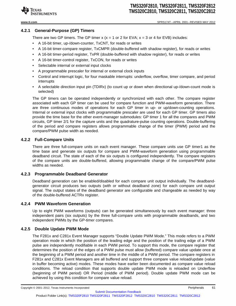
TMS320F2810, TMS320F2811, TMS320F2812TMS320C2810, TMS320C2811, TMS320C2812
www.ti.com SPRS174T –APRIL 2001–REVISED MAY 2012
4.2.1 General-Purpose (GP) Timers
There are two GP timers. The GP timer x (x = 1 or 2 for EVA; x = 3 or 4 for EVB) includes:• A 16-bit timer, up-/down-counter, TxCNT, for reads or writes• A 16-bit timer-compare register, TxCMPR (double-buffered with shadow register), for reads or writes• A 16-bit timer-period register, TxPR (double-buffered with shadow register), for reads or writes• A 16-bit timer-control register, TxCON, for reads or writes• Selectable internal or external input clocks• A programmable prescaler for internal or external clock inputs• Control and interrupt logic, for four maskable interrupts: underflow, overflow, timer compare, and period
interrupts• A selectable direction input pin (TDIRx) (to count up or down when directional up-/down-count mode is
selected)
The GP timers can be operated independently or synchronized with each other. The compare registerassociated with each GP timer can be used for compare function and PWM-waveform generation. Thereare three continuous modes of operations for each GP timer in up- or up/down-counting operations.Internal or external input clocks with programmable prescaler are used for each GP timer. GP timers alsoprovide the time base for the other event-manager submodules: GP timer 1 for all the compares and PWMcircuits, GP timer 2/1 for the capture units and the quadrature-pulse counting operations. Double-bufferingof the period and compare registers allows programmable change of the timer (PWM) period and thecompare/PWM pulse width as needed.
4.2.2 Full-Compare Units
There are three full-compare units on each event manager. These compare units use GP timer1 as thetime base and generate six outputs for compare and PWM-waveform generation using programmabledeadband circuit. The state of each of the six outputs is configured independently. The compare registersof the compare units are double-buffered, allowing programmable change of the compare/PWM pulsewidths as needed.
4.2.3 Programmable Deadband Generator
Deadband generation can be enabled/disabled for each compare unit output individually. The deadband-generator circuit produces two outputs (with or without deadband zone) for each compare unit outputsignal. The output states of the deadband generator are configurable and changeable as needed by wayof the double-buffered ACTRx register.
4.2.4 PWM Waveform Generation
Up to eight PWM waveforms (outputs) can be generated simultaneously by each event manager: threeindependent pairs (six outputs) by the three full-compare units with programmable deadbands, and twoindependent PWMs by the GP-timer compares.
4.2.5 Double Update PWM Mode
The F281x and C281x Event Manager supports “Double Update PWM Mode.” This mode refers to a PWMoperation mode in which the position of the leading edge and the position of the trailing edge of a PWMpulse are independently modifiable in each PWM period. To support this mode, the compare register thatdetermines the position of the edges of a PWM pulse must allow (buffered) compare value update once atthe beginning of a PWM period and another time in the middle of a PWM period. The compare registers inF281x and C281x Event Managers are all buffered and support three compare value reload/update (valuein buffer becoming active) modes. These modes have earlier been documented as compare value reloadconditions. The reload condition that supports double update PWM mode is reloaded on Underflow(beginning of PWM period) OR Period (middle of PWM period). Double update PWM mode can beachieved by using this condition for compare value reload.
Copyright © 2001–2012, Texas Instruments Incorporated Peripherals 61Submit Documentation Feedback
Product Folder Link(s): TMS320F2810 TMS320F2811 TMS320F2812 TMS320C2810 TMS320C2811 TMS320C2812

TMS320F2810, TMS320F2811, TMS320F2812TMS320C2810, TMS320C2811, TMS320C2812
SPRS174T –APRIL 2001–REVISED MAY 2012 www.ti.com
4.2.6 PWM Characteristics
Characteristics of the PWMs are as follows:• 16-bit registers• Wide range of programmable deadband for the PWM output pairs• Change of the PWM carrier frequency for PWM frequency wobbling as needed• Change of the PWM pulse widths within and after each PWM period as needed• External-maskable power and drive-protection interrupts• Pulse-pattern-generator circuit, for programmable generation of asymmetric, symmetric, and four-
space vector PWM waveforms• Minimized CPU overhead using auto-reload of the compare and period registers• The PWM pins are driven to a high-impedance state when the PDPINTx pin is driven low and after
PDPINTx signal qualification. The PDPINTx pin (after qualification) is reflected in bit 8 of theCOMCONx register.– PDPINTA pin status is reflected in bit 8 of COMCONA register.– PDPINTB pin status is reflected in bit 8 of COMCONB register.
• EXTCON register bits provide options to individually trip control for each PWM pair of signals
4.2.7 Capture Unit
The capture unit provides a logging function for different events or transitions. The values of the selectedGP timer counter is captured and stored in the two-level-deep FIFO stacks when selected transitions aredetected on capture input pins, CAPx (x = 1, 2, or 3 for EVA; and x = 4, 5, or 6 for EVB). The capture unitconsists of three capture circuits.
Capture units include the following features:• One 16-bit capture control register, CAPCONx (R/W)• One 16-bit capture FIFO status register, CAPFIFOx• Selection of GP timer 1/2 (for EVA) or 3/4 (for EVB) as the time base• Three 16-bit 2-level-deep FIFO stacks, one for each capture unit• Three capture input pins (CAP1/2/3 for EVA, CAP4/5/6 for EVB)—one input pin per capture unit. [All
inputs are synchronized with the device (CPU) clock. In order for a transition to be captured, the inputmust hold at its current level to meet the input qualification circuitry requirements. The input pinsCAP1/2 and CAP4/5 can also be used as QEP inputs to the QEP circuit.]
• User-specified transition (rising edge, falling edge, or both edges) detection• Three maskable interrupt flags, one for each capture unit• The capture pins can also be used as general-purpose interrupt pins, if they are not used for the
capture function.
4.2.8 Quadrature-Encoder Pulse (QEP) Circuit
Two capture inputs (CAP1 and CAP2 for EVA; CAP4 and CAP5 for EVB) can be used to interface the on-chip QEP circuit with a quadrature encoder pulse. Full synchronization of these inputs is performed on-chip. Direction or leading-quadrature pulse sequence is detected, and GP timer 2/4 is incremented ordecremented by the rising and falling edges of the two input signals (four times the frequency of eitherinput pulse).
With EXTCONA register bits, the EVA QEP circuit can use CAP3 as a capture index pin as well. Similarly,with EXTCONB register bits, the EVB QEP circuit can use CAP6 as a capture index pin.
4.2.9 External ADC Start-of-Conversion
EVA/EVB start-of-conversion (SOC) can be sent to an external pin (EVASOC/EVBSOC) for external ADCinterface. EVASOC and EVBSOC are MUXed with T2CTRIP and T4CTRIP, respectively.
62 Peripherals Copyright © 2001–2012, Texas Instruments Incorporated
Submit Documentation FeedbackProduct Folder Link(s): TMS320F2810 TMS320F2811 TMS320F2812 TMS320C2810 TMS320C2811 TMS320C2812

0,ValueDigital = V0inputwhen £
4095,ValueDigital = V3inputwhen ³
V3inputV0when <<
3
ADCLOVoltageAnalogInput4096ValueDigital
-´=
TMS320F2810, TMS320F2811, TMS320F2812TMS320C2810, TMS320C2811, TMS320C2812
www.ti.com SPRS174T –APRIL 2001–REVISED MAY 2012
4.3 Enhanced Analog-to-Digital Converter (ADC) Module
A simplified functional block diagram of the ADC module is shown in Figure 4-4. The ADC moduleconsists of a 12-bit ADC with a built-in sample-and-hold (S/H) circuit. Functions of the ADC moduleinclude:• 12-bit ADC core with built-in S/H• Analog input: 0.0 V to 3.0 V (voltages above 3.0 V produce full-scale conversion results)• Fast conversion rate: 80 ns at 25-MHz ADC clock, 12.5 MSPS• 16-channel, MUXed inputs• Autosequencing capability provides up to 16 “autoconversions” in a single session. Each conversion
can be programmed to select any 1 of 16 input channels• Sequencer can be operated as two independent 8-state sequencers or as one large 16-state
sequencer (that is, two cascaded 8-state sequencers)• Sixteen result registers (individually addressable) to store conversion values
– The digital value of the input analog voltage is derived by:
• Multiple triggers as sources for the start-of-conversion (SOC) sequence– S/W – software immediate start– EVA – Event manager A (multiple event sources within EVA)– EVB – Event manager B (multiple event sources within EVB)
• Flexible interrupt control allows interrupt request on every end-of-sequence (EOS) or every other EOS• Sequencer can operate in “start/stop” mode, allowing multiple “time-sequenced triggers” to synchronize
conversions• EVA and EVB triggers can operate independently in dual-sequencer mode• Sample-and-hold (S/H) acquisition time window has separate prescale control
The ADC module in the F281x and C281x has been enhanced to provide flexible interface to eventmanagers A and B. The ADC interface is built around a fast, 12-bit ADC module with a fast conversionrate of 80 ns at 25-MHz ADC clock. The ADC module has 16 channels, configurable as two independent8-channel modules to service event managers A and B. The two independent 8-channel modules can becascaded to form a 16-channel module. Although there are multiple input channels and two sequencers,there is only one converter in the ADC module. Figure 4-4 shows the block diagram of the F281x andC281x ADC module.
The two 8-channel modules have the capability to autosequence a series of conversions, each modulehas the choice of selecting any one of the respective eight channels available through an analog MUX. Inthe cascaded mode, the autosequencer functions as a single 16-channel sequencer. On each sequencer,once the conversion is complete, the selected channel value is stored in its respective RESULT register.Autosequencing allows the system to convert the same channel multiple times, allowing the user toperform oversampling algorithms. This gives increased resolution over traditional single-sampledconversion results.
Copyright © 2001–2012, Texas Instruments Incorporated Peripherals 63Submit Documentation Feedback
Product Folder Link(s): TMS320F2810 TMS320F2811 TMS320F2812 TMS320C2810 TMS320C2811 TMS320C2812

Result Registers
EVB
S/W
ADC Control Registers
70B7h
70B0h
70AFh
70A8h
Result Reg 15
Result Reg 8
Result Reg 7
Result Reg 1
Result Reg 0
12-BitADC
Module
AnalogMUX
EVA
S/W
ADCINA0
ADCINA7
ADCINB0
ADCINB7
ADCSOC
SystemControl Block
High-SpeedPrescaler
HSPCLK
C28xSYSCLKOUT
S/H
S/H
ADCENCLK
Sequencer 2Sequencer 1 SOCSOC
TMS320F2810, TMS320F2811, TMS320F2812TMS320C2810, TMS320C2811, TMS320C2812
SPRS174T –APRIL 2001–REVISED MAY 2012 www.ti.com
Figure 4-4. Block Diagram of the F281x and C281x ADC Module
To obtain the specified accuracy of the ADC, proper board layout is critical. To the best extent possible,traces leading to the ADCIN pins should not run in close proximity to the digital signal paths. This is tominimize switching noise on the digital lines from getting coupled to the ADC inputs. Furthermore, properisolation techniques must be used to isolate the ADC module power pins (VDDA1/VDDA2, AVDDREFBG)from the digital supply. For better accuracy and ESD protection, unused ADC inputs should be connectedto analog ground.
Notes:
1. The ADC registers are accessed at the SYSCLKOUT rate. The internal timing of the ADC module iscontrolled by the high-speed peripheral clock (HSPCLK).
2. The behavior of the ADC module based on the state of the ADCENCLK and HALT signals is asfollows:
ADCENCLK: On reset, this signal will be low. While reset is active-low (XRS) the clock to the registerwill still function. This is necessary to make sure all registers and modes go into their default resetstate. The analog module will, however, be in a low-power inactive state. As soon as reset goes high,then the clock to the registers will be disabled. When the user sets the ADCENCLK signal high, thenthe clocks to the registers will be enabled and the analog module will be enabled. There will be acertain time delay (ms range) before the ADC is stable and can be used.
HALT: This signal only affects the analog module. It does not affect the registers. If low, the ADCmodule is powered. If high, the ADC module goes into low-power mode. The HALT mode will stop theclock to the CPU, which will stop the HSPCLK. Therefore the ADC register logic will be turned offindirectly.
64 Peripherals Copyright © 2001–2012, Texas Instruments Incorporated
Submit Documentation FeedbackProduct Folder Link(s): TMS320F2810 TMS320F2811 TMS320F2812 TMS320C2810 TMS320C2811 TMS320C2812

ADCINA[7:0]ADCINB[7:0]
ADCLO
ADCBGREFIN(A)
Test Pin
ADC External Current Bias Resistor ADCRESEXT
ADCREFP
VDDA1
VDDA2
VSSA1
VSSA2
AVDDREFBG
AVSSREFBG
VDDAIO
VSSAIO
VDD1
VSS1
ADC Reference Positive Output
ADCREFMADC Reference Medium Output
ADC Analog Power
ADC Reference Power
ADC Analog I/O Power
ADC Digital Power
Analog input 0-3 V with respect to ADCLO
Connect to Analog Ground
Analog 3.3 V
Analog 3.3 V
Analog 3.3 V
Analog 3.3 V
Analog Ground
1.8 V
ADCREFP and ADCREFM should notbe loaded by external circuitry
can use the same 1.8-V (or 1.9-V) supply asthe digital core but separate the two with aferrite bead or a filter
Digital Ground
ADC 16-Channel Analog Inputs
10 Fμ(C)
10 Fμ(C)
24.9 k /20 k(B)
TMS320F2810, TMS320F2811, TMS320F2812TMS320C2810, TMS320C2811, TMS320C2812
www.ti.com SPRS174T –APRIL 2001–REVISED MAY 2012
Figure 4-5 shows the ADC pin-biasing for internal reference and Figure 4-6 shows the ADC pin-biasing forexternal reference.
A. Provide access to this pin in PCB layouts. Intended for test purposes only.B. Use 24.9 kΩ for ADC clock range 1–18.75 MHz; use 20 kΩ for ADC clock range 18.75–25 MHz.C. TAIYO YUDEN EMK325F106ZH, EMK325BJ106MD, or equivalent ceramic capacitorD. External decoupling capacitors are recommended on all power pins.E. Analog inputs must be driven from an operational amplifier that does not degrade the ADC performance.
Figure 4-5. ADC Pin Connections With Internal Reference
NOTEThe temperature rating of any recommended component must match the rating of the endproduct.
Copyright © 2001–2012, Texas Instruments Incorporated Peripherals 65Submit Documentation Feedback
Product Folder Link(s): TMS320F2810 TMS320F2811 TMS320F2812 TMS320C2810 TMS320C2811 TMS320C2812

ADCINA[7:0]
ADCINB[7:0]
ADCLO
ADCBGREFIN
ADC External Current Bias Resistor ADCRESEXT
ADCREFP
VDDA1
VDDA2
VSSA1
VSSA2
AVDDREFBG
AVSSREFBG
VDDAIO
VSSAIO
VDD1
VSS1
Test Pin
ADC Reference Positive Input
ADCREFMADC Reference Medium Input
ADC Analog Power
ADC Reference Power
ADC Analog I/O Power
ADC Digital Power
Analog Input 0-3 V With Respect to ADCLO
Connect to Analog Ground
Analog 3.3 V
Analog 3.3 V
Analog 3.3 V
Analog 3.3 V
Analog Ground
1.8 V can use the same 1.8-V (or 1.9-V)supply as the digital core but separate thetwo with a ferrite bead or a filter
Digital Ground
ADC 16-Channel Analog Inputs
2 V
1 V(D)
1 F -μ 10 Fμ1 F -μ 10 Fμ
24.9 k /20 k(C)
TMS320F2810, TMS320F2811, TMS320F2812TMS320C2810, TMS320C2811, TMS320C2812
SPRS174T –APRIL 2001–REVISED MAY 2012 www.ti.com
A. External decoupling capacitors are recommended on all power pins.B. Analog inputs must be driven from an operational amplifier that does not degrade the ADC performance.C. Use 24.9 kΩ for ADC clock range 1–18.75 MHz; use 20 kΩ for ADC clock range 18.75–25 MHz.D. It is recommended that buffered external references be provided with a voltage difference of (ADCREFP –
ADCREFM) = 1 V ± 0.1% or better.External reference is enabled using bit 8 in the ADCTRL3 Register at ADC power up. In this mode, the accuracy ofexternal reference is critical for overall gain. The voltage ADCREFP – ADCREFM will determine the overall accuracy.Do not enable internal references when external references are connected to ADCREFP and ADCREFM. See theTMS320x281x DSP Analog-to-Digital Converter (ADC) Reference Guide (literature number SPRU060) for moreinformation.
Figure 4-6. ADC Pin Connections With External Reference
66 Peripherals Copyright © 2001–2012, Texas Instruments Incorporated
Submit Documentation FeedbackProduct Folder Link(s): TMS320F2810 TMS320F2811 TMS320F2812 TMS320C2810 TMS320C2811 TMS320C2812

TMS320F2810, TMS320F2811, TMS320F2812TMS320C2810, TMS320C2811, TMS320C2812
www.ti.com SPRS174T –APRIL 2001–REVISED MAY 2012
The ADC operation is configured, controlled, and monitored by the registers listed in Table 4-4.
Table 4-4. ADC Registers (1)
NAME ADDRESS SIZE (x16) DESCRIPTION
ADCTRL1 0x00 7100 1 ADC Control Register 1
ADCTRL2 0x00 7101 1 ADC Control Register 2
ADCMAXCONV 0x00 7102 1 ADC Maximum Conversion Channels Register
ADCCHSELSEQ1 0x00 7103 1 ADC Channel Select Sequencing Control Register 1
ADCCHSELSEQ2 0x00 7104 1 ADC Channel Select Sequencing Control Register 2
ADCCHSELSEQ3 0x00 7105 1 ADC Channel Select Sequencing Control Register 3
ADCCHSELSEQ4 0x00 7106 1 ADC Channel Select Sequencing Control Register 4
ADCASEQSR 0x00 7107 1 ADC Auto-Sequence Status Register
ADCRESULT0 0x00 7108 1 ADC Conversion Result Buffer Register 0
ADCRESULT1 0x00 7109 1 ADC Conversion Result Buffer Register 1
ADCRESULT2 0x00 710A 1 ADC Conversion Result Buffer Register 2
ADCRESULT3 0x00 710B 1 ADC Conversion Result Buffer Register 3
ADCRESULT4 0x00 710C 1 ADC Conversion Result Buffer Register 4
ADCRESULT5 0x00 710D 1 ADC Conversion Result Buffer Register 5
ADCRESULT6 0x00 710E 1 ADC Conversion Result Buffer Register 6
ADCRESULT7 0x00 710F 1 ADC Conversion Result Buffer Register 7
ADCRESULT8 0x00 7110 1 ADC Conversion Result Buffer Register 8
ADCRESULT9 0x00 7111 1 ADC Conversion Result Buffer Register 9
ADCRESULT10 0x00 7112 1 ADC Conversion Result Buffer Register 10
ADCRESULT11 0x00 7113 1 ADC Conversion Result Buffer Register 11
ADCRESULT12 0x00 7114 1 ADC Conversion Result Buffer Register 12
ADCRESULT13 0x00 7115 1 ADC Conversion Result Buffer Register 13
ADCRESULT14 0x00 7116 1 ADC Conversion Result Buffer Register 14
ADCRESULT15 0x00 7117 1 ADC Conversion Result Buffer Register 15
ADCTRL3 0x00 7118 1 ADC Control Register 3
ADCST 0x00 7119 1 ADC Status Register
Reserved 0x00 711C – 0x00 711F 4
(1) The above registers are Peripheral Frame 2 Registers.
Copyright © 2001–2012, Texas Instruments Incorporated Peripherals 67Submit Documentation Feedback
Product Folder Link(s): TMS320F2810 TMS320F2811 TMS320F2812 TMS320C2810 TMS320C2811 TMS320C2812

TMS320F2810, TMS320F2811, TMS320F2812TMS320C2810, TMS320C2811, TMS320C2812
SPRS174T –APRIL 2001–REVISED MAY 2012 www.ti.com
4.4 Enhanced Controller Area Network (eCAN) Module
The CAN module has the following features:• Fully compliant with CAN protocol, version 2.0B• Supports data rates up to 1 Mbps• Thirty-two mailboxes, each with the following properties:
– Configurable as receive or transmit– Configurable with standard or extended identifier– Has a programmable receive mask– Supports data and remote frame– Composed of 0 to 8 bytes of data– Uses a 32-bit time stamp on receive and transmit message– Protects against reception of new message– Holds the dynamically programmable priority of transmit message– Employs a programmable interrupt scheme with two interrupt levels– Employs a programmable alarm on transmission or reception time-out
• Low-power mode• Programmable wake-up on bus activity• Automatic reply to a remote request message• Automatic retransmission of a frame in case of loss of arbitration or error• 32-bit local network time counter synchronized by a specific message (communication in conjunction
with mailbox 16)• Self-test mode
– Operates in a loopback mode receiving its own message. A “dummy” acknowledge is provided,thereby eliminating the need for another node to provide the acknowledge bit.
NOTE: For a SYSCLKOUT of 150 MHz, the smallest bit rate possible is 23.4 kbps.
The 28x CAN has passed the conformance test per ISO/DIS 16845. Contact TI for details.
68 Peripherals Copyright © 2001–2012, Texas Instruments Incorporated
Submit Documentation FeedbackProduct Folder Link(s): TMS320F2810 TMS320F2811 TMS320F2812 TMS320C2810 TMS320C2811 TMS320C2812

Mailbox RAM(512 Bytes)
32-Message Mailboxof 4 x 32-Bit Words
Memory ManagementUnit
CPU Interface,Receive Control Unit,
Timer Management Unit
eCAN Memory(512 Bytes)
Registers andMessage Objects Control
Message Controller
32 32
eCAN Protocol Kernel
Receive Buffer
Transmit Buffer
Control Buffer
Status Buffer
Enhanced CAN Controller 32
Controls Address DataeCAN1INTeCAN0INT
32
SN65HVD23x3.3-V CAN Transceiver
CAN Bus
TMS320F2810, TMS320F2811, TMS320F2812TMS320C2810, TMS320C2811, TMS320C2812
www.ti.com SPRS174T –APRIL 2001–REVISED MAY 2012
Figure 4-7. eCAN Block Diagram and Interface Circuit
Copyright © 2001–2012, Texas Instruments Incorporated Peripherals 69Submit Documentation Feedback
Product Folder Link(s): TMS320F2810 TMS320F2811 TMS320F2812 TMS320C2810 TMS320C2811 TMS320C2812

TMS320F2810, TMS320F2811, TMS320F2812TMS320C2810, TMS320C2811, TMS320C2812
SPRS174T –APRIL 2001–REVISED MAY 2012 www.ti.com
Table 4-5. 3.3-V eCAN Transceivers for the TMS320F281x and TMS320C281x DSPs
PART SUPPLY LOW-POWER SLOPE VREF OTHER TANUMBER VOLTAGE MODE CONTROL
SN65HVD230 3.3 V Standby Adjustable Yes – –40°C to 85°C
SN65HVD230Q 3.3 V Standby Adjustable Yes – –40°C to 125°C
SN65HVD231 3.3 V Sleep Adjustable Yes – –40°C to 85°C
SN65HVD231Q 3.3 V Sleep Adjustable Yes – –40°C to 125°C
SN65HVD232 3.3 V None None None – –40°C to 85°C
SN65HVD232Q 3.3 V None None None – –40°C to 125°C
SN65HVD233 3.3 V Standby Adjustable None Diagnostic Loopback –40°C to 125°C
StandbySN65HVD234 3.3 V and Adjustable None – –40°C to 125°C
Sleep
SN65HVD235 3.3 V Standby Adjustable None Autobaud Loopback –40°C to 125°C
Built-in IsolationLow Prop Delay
ISO1050 3–5.5 V None None None Thermal Shutdown –55°C to 105°CFailsafe OperationDominant Time-out
70 Peripherals Copyright © 2001–2012, Texas Instruments Incorporated
Submit Documentation FeedbackProduct Folder Link(s): TMS320F2810 TMS320F2811 TMS320F2812 TMS320C2810 TMS320C2811 TMS320C2812

Mailbox Enable - CANME
Mailbox Direction - CANMD
Transmission Request Set - CANTRS
Transmission Request Reset - CANTRR
Transmission Acknowledge - CANTA
Abort Acknowledge - CANAA
Received Message Pending - CANRMP
Received Message Lost - CANRML
Remote Frame Pending - CANRFP
Global Acceptance Mask - CANGAM
Master Control - CANMC
Bit-Timing Configuration - CANBTC
Error and Status - CANES
Transmit Error Counter - CANTEC
Receive Error Counter - CANREC
Global Interrupt Flag 0 - CANGIF0
Global Interrupt Mask - CANGIM
Mailbox Interrupt Mask - CANMIM
Mailbox Interrupt Level - CANMIL
Overwrite Protection Control - CANOPC
TX I/O Control - CANTIOC
RX I/O Control - CANRIOC
Time Stamp Counter - CANTSC
Global Interrupt Flag 1 - CANGIF1
Time-Out Control - CANTOC
Time-Out Status - CANTOS
Reserved
eCAN Control and Status Registers
Message Identifier - MSGID61E8h-61E9h
Message Control - MSGCTRL
Message Data Low - MDL
Message Data High - MDH
Message Mailbox (16 Bytes)
Control and Status Registers
6000h
603Fh
Local Acceptance Masks (LAM)(32 x 32-Bit RAM)
6040h
607Fh6080h
60BFh60C0h
60FFh
eCAN Memory (512 Bytes)
Message Object Time Stamps (MOTS)(32 x 32-Bit RAM)
Message Object Time-Out (MOTO)(32 x 32-Bit RAM)
Mailbox 06100h-6107h
Mailbox 16108h-610Fh
Mailbox 26110h-6117h
Mailbox 36118h-611Fh
eCAN Memory RAM (512 Bytes)
Mailbox 46120h-6127h
Mailbox 2861E0h-61E7h
Mailbox 2961E8h-61EFh
Mailbox 3061F0h-61F7h
Mailbox 3161F8h-61FFh
61EAh-61EBh
61ECh-61EDh
61EEh-61EFh
TMS320F2810, TMS320F2811, TMS320F2812TMS320C2810, TMS320C2811, TMS320C2812
www.ti.com SPRS174T –APRIL 2001–REVISED MAY 2012
Figure 4-8. eCAN Memory Map
NOTEIf the eCAN module is not used in an application, the RAM available (LAM, MOTS, MOTO,and mailbox RAM) can be used as general-purpose RAM. The CAN module clock should beenabled for this.
Copyright © 2001–2012, Texas Instruments Incorporated Peripherals 71Submit Documentation Feedback
Product Folder Link(s): TMS320F2810 TMS320F2811 TMS320F2812 TMS320C2810 TMS320C2811 TMS320C2812

TMS320F2810, TMS320F2811, TMS320F2812TMS320C2810, TMS320C2811, TMS320C2812
SPRS174T –APRIL 2001–REVISED MAY 2012 www.ti.com
The CAN registers listed in Table 4-6 are used by the CPU to configure and control the CAN controllerand the message objects. eCAN control registers only support 32-bit read/write operations. Mailbox RAMcan be accessed as 16 bits or 32 bits. 32-bit accesses are aligned to an even boundary.
Table 4-6. CAN Registers (1)
NAME ADDRESS SIZE (x32) DESCRIPTION
CANME 0x00 6000 1 Mailbox enable
CANMD 0x00 6002 1 Mailbox direction
CANTRS 0x00 6004 1 Transmit request set
CANTRR 0x00 6006 1 Transmit request reset
CANTA 0x00 6008 1 Transmission acknowledge
CANAA 0x00 600A 1 Abort acknowledge
CANRMP 0x00 600C 1 Receive message pending
CANRML 0x00 600E 1 Receive message lost
CANRFP 0x00 6010 1 Remote frame pending
CANGAM 0x00 6012 1 Global acceptance mask
CANMC 0x00 6014 1 Master control
CANBTC 0x00 6016 1 Bit-timing configuration
CANES 0x00 6018 1 Error and status
CANTEC 0x00 601A 1 Transmit error counter
CANREC 0x00 601C 1 Receive error counter
CANGIF0 0x00 601E 1 Global interrupt flag 0
CANGIM 0x00 6020 1 Global interrupt mask
CANGIF1 0x00 6022 1 Global interrupt flag 1
CANMIM 0x00 6024 1 Mailbox interrupt mask
CANMIL 0x00 6026 1 Mailbox interrupt level
CANOPC 0x00 6028 1 Overwrite protection control
CANTIOC 0x00 602A 1 TX I/O control
CANRIOC 0x00 602C 1 RX I/O control
CANTSC 0x00 602E 1 Time stamp counter (Reserved in SCC mode)
CANTOC 0x00 6030 1 Time-out control (Reserved in SCC mode)
CANTOS 0x00 6032 1 Time-out status (Reserved in SCC mode)
(1) These registers are mapped to Peripheral Frame 1.
72 Peripherals Copyright © 2001–2012, Texas Instruments Incorporated
Submit Documentation FeedbackProduct Folder Link(s): TMS320F2810 TMS320F2811 TMS320F2812 TMS320C2810 TMS320C2811 TMS320C2812

TMS320F2810, TMS320F2811, TMS320F2812TMS320C2810, TMS320C2811, TMS320C2812
www.ti.com SPRS174T –APRIL 2001–REVISED MAY 2012
4.5 Multichannel Buffered Serial Port (McBSP) Module
The McBSP module has the following features:• Compatible to McBSP in TMS320C54x™/ TMS320C55x™ DSP devices, except the DMA features• Full-duplex communication• Double-buffered data registers which allow a continuous data stream• Independent framing and clocking for receive and transmit• External shift clock generation or an internal programmable frequency shift clock• A wide selection of data sizes including 8-, 12-, 16-, 20-, 24-, or 32-bits• 8-bit data transfers with LSB or MSB first• Programmable polarity for both frame synchronization and data clocks• Highly programmable internal clock and frame generation• Support A-bis mode• Direct interface to industry-standard CODECs, Analog Interface Chips (AICs), and other serially
connected A/D and D/A devices• Works with SPI-compatible devices• Two 16 x 16-level FIFO for Transmit channel• Two 16 x 16-level FIFO for Receive channel
The following application interfaces can be supported on the McBSP:• T1/E1 framers• MVIP switching-compatible and ST-BUS-compliant devices including:
– MVIP framers– H.100 framers– SCSA framers– IOM-2 compliant devices– AC97-compliant devices (the necessary multiphase frame synchronization capability is provided.)– IIS-compliant devices
• McBSP clock rate = CLKG = CLKSRG/(1 + CLKGDIV) , where CLKSRG source could be LSPCLK,CLKX, or CLKR. (2)
(2) Serial port performance is limited by I/O buffer switching speed. Internal prescalers must be adjusted such that the peripheral speed isless than the I/O buffer speed limit—20-MHz maximum.
Copyright © 2001–2012, Texas Instruments Incorporated Peripherals 73Submit Documentation Feedback
Product Folder Link(s): TMS320F2810 TMS320F2811 TMS320F2812 TMS320C2810 TMS320C2811 TMS320C2812

McBSP ReceiveInterrupt Select Logic
DX
DR
Expand Logic
RX FIFOInterrupt
DRR2 Receive Buffer
RX FIFO Registers
RBR1 RegisterRBR2 Register
McBSP Registersand
Control Logic CLKX
FSX
CLKR
FSR
16
Compand Logic
DXR2 Transmit Buffer
RSR1
XSR2 XSR1
Peripheral Read Bus
16
1616
1616
RSR2
DXR1 Transmit Buffer
16
LSPCLK
MRINT
To CPU
McBSP
RX Interrupt Logic
RX FIFO _15
RX FIFO _1
RX FIFO _0
RX FIFO _15
RX FIFO _1
RX FIFO _0
McBSP TransmitInterrupt Select Logic
TX FIFOInterrupt
TX FIFO Registers
MXINT
To CPU TX Interrupt Logic
16 16
16
TX FIFO _15
TX FIFO _1
TX FIFO _0
TX FIFO _15
TX FIFO _1
TX FIFO _0
Peripheral Write Bus
DRR1 Receive Buffer
TMS320F2810, TMS320F2811, TMS320F2812TMS320C2810, TMS320C2811, TMS320C2812
SPRS174T –APRIL 2001–REVISED MAY 2012 www.ti.com
Figure 4-9 shows the block diagram of the McBSP module with FIFO, interfaced to the F281x and C281xversion of Peripheral Frame 2.
Figure 4-9. McBSP Module With FIFO
74 Peripherals Copyright © 2001–2012, Texas Instruments Incorporated
Submit Documentation FeedbackProduct Folder Link(s): TMS320F2810 TMS320F2811 TMS320F2812 TMS320C2810 TMS320C2811 TMS320C2812

TMS320F2810, TMS320F2811, TMS320F2812TMS320C2810, TMS320C2811, TMS320C2812
www.ti.com SPRS174T –APRIL 2001–REVISED MAY 2012
Table 4-7 provides a summary of the McBSP registers.
Table 4-7. McBSP Registers
ADDRESS TYPE RESET VALUENAME DESCRIPTION0x00 78xxh (R/W) (HEX)
DATA REGISTERS, RECEIVE, TRANSMIT (1)
– – – 0x0000 McBSP Receive Buffer Register
– – – 0x0000 McBSP Receive Shift Register
– – – 0x0000 McBSP Transmit Shift Register
McBSP Data Receive Register 2DRR2 00 R 0x0000 • Read First if the word size is greater than 16 bits,
else ignore DRR2
McBSP Data Receive Register 1DRR1 01 R 0x0000 • Read Second if the word size is greater than 16 bits,
else read DRR1 only
McBSP Data Transmit Register 2DXR2 02 W 0x0000 • Write First if the word size is greater than 16 bits,
else ignore DXR2
McBSP Data Transmit Register 1DXR1 03 W 0x0000 • Write Second if the word size is greater than 16 bits,
else write to DXR1 only
McBSP CONTROL REGISTERS
SPCR2 04 R/W 0x0000 McBSP Serial Port Control Register 2
SPCR1 05 R/W 0x0000 McBSP Serial Port Control Register 1
RCR2 06 R/W 0x0000 McBSP Receive Control Register 2
RCR1 07 R/W 0x0000 McBSP Receive Control Register 1
XCR2 08 R/W 0x0000 McBSP Transmit Control Register 2
XCR1 09 R/W 0x0000 McBSP Transmit Control Register 1
SRGR2 0A R/W 0x0000 McBSP Sample Rate Generator Register 2
SRGR1 0B R/W 0x0000 McBSP Sample Rate Generator Register 1
MULTICHANNEL CONTROL REGISTERS
MCR2 0C R/W 0x0000 McBSP Multichannel Register 2
MCR1 0D R/W 0x0000 McBSP Multichannel Register 1
RCERA 0E R/W 0x0000 McBSP Receive Channel Enable Register Partition A
RCERB 0F R/W 0x0000 McBSP Receive Channel Enable Register Partition B
XCERA 10 R/W 0x0000 McBSP Transmit Channel Enable Register Partition A
XCERB 11 R/W 0x0000 McBSP Transmit Channel Enable Register Partition B
PCR 12 R/W 0x0000 McBSP Pin Control Register
RCERC 13 R/W 0x0000 McBSP Receive Channel Enable Register Partition C
RCERD 14 R/W 0x0000 McBSP Receive Channel Enable Register Partition D
XCERC 15 R/W 0x0000 McBSP Transmit Channel Enable Register Partition C
XCERD 16 R/W 0x0000 McBSP Transmit Channel Enable Register Partition D
RCERE 17 R/W 0x0000 McBSP Receive Channel Enable Register Partition E
RCERF 18 R/W 0x0000 McBSP Receive Channel Enable Register Partition F
XCERE 19 R/W 0x0000 McBSP Transmit Channel Enable Register Partition E
XCERF 1A R/W 0x0000 McBSP Transmit Channel Enable Register Partition F
RCERG 1B R/W 0x0000 McBSP Receive Channel Enable Register Partition G
RCERH 1C R/W 0x0000 McBSP Receive Channel Enable Register Partition H
XCERG 1D R/W 0x0000 McBSP Transmit Channel Enable Register Partition G
XCERH 1E R/W 0x0000 McBSP Transmit Channel Enable Register Partition H
(1) DRR2/DRR1 and DXR2/DXR1 share the same addresses of receive and transmit FIFO registers in FIFO mode.
Copyright © 2001–2012, Texas Instruments Incorporated Peripherals 75Submit Documentation Feedback
Product Folder Link(s): TMS320F2810 TMS320F2811 TMS320F2812 TMS320C2810 TMS320C2811 TMS320C2812

TMS320F2810, TMS320F2811, TMS320F2812TMS320C2810, TMS320C2811, TMS320C2812
SPRS174T –APRIL 2001–REVISED MAY 2012 www.ti.com
Table 4-7. McBSP Registers (continued)
ADDRESS TYPE RESET VALUENAME DESCRIPTION0x00 78xxh (R/W) (HEX)
FIFO MODE REGISTERS (applicable only in FIFO mode)
FIFO Data Registers (2)
McBSP Data Receive Register 2 – Top of receive FIFODRR2 00 R 0x0000
• Read First FIFO pointers will not advance
McBSP Data Receive Register 1 – Top of receive FIFODRR1 01 R 0x0000
• Read Second for FIFO pointers to advance
McBSP Data Transmit Register 2 – Top of transmit FIFODXR2 02 W 0x0000
• Write First FIFO pointers will not advance
McBSP Data Transmit Register 1 – Top of transmit FIFODXR1 03 W 0x0000
• Write Second for FIFO pointers to advance
FIFO Control Registers
MFFTX 20 R/W 0xA000 McBSP Transmit FIFO Register
MFFRX 21 R/W 0x201F McBSP Receive FIFO Register
MFFCT 22 R/W 0x0000 McBSP FIFO Control Register
MFFINT 23 R/W 0x0000 McBSP FIFO Interrupt Register
MFFST 24 R/W 0x0000 McBSP FIFO Status Register
(2) FIFO pointers advancing is based on order of access to DRR2/DRR1 and DXR2/DXR1 registers.
76 Peripherals Copyright © 2001–2012, Texas Instruments Incorporated
Submit Documentation FeedbackProduct Folder Link(s): TMS320F2810 TMS320F2811 TMS320F2812 TMS320C2810 TMS320C2811 TMS320C2812

rateBaud8*1)(BRR
LSPCLK
+
= 0BRRwhen ¹
16
LSPCLK= 0BRRwhen =
TMS320F2810, TMS320F2811, TMS320F2812TMS320C2810, TMS320C2811, TMS320C2812
www.ti.com SPRS174T –APRIL 2001–REVISED MAY 2012
4.6 Serial Communications Interface (SCI) Module
The F281x and C281x devices include two serial communications interface (SCI) modules. The SCImodules support digital communications between the CPU and other asynchronous peripherals that usethe standard non-return-to-zero (NRZ) format. The SCI receiver and transmitter are double-buffered, andeach has its own separate enable and interrupt bits. Both can be operated independently orsimultaneously in the full-duplex mode. To ensure data integrity, the SCI checks received data for breakdetection, parity, overrun, and framing errors. The bit rate is programmable to over 65000 different speedsthrough a 16-bit baud-select register.
Features of each SCI module include:• Two external pins:
– SCITXD: SCI transmit-output pin– SCIRXD: SCI receive-input pinNOTE: Both pins can be used as GPIO if not used for SCI.
• Baud rate programmable to 64K different rates (3)
• Data-word format– One start bit– Data-word length programmable from one to eight bits– Optional even/odd/no parity bit– One or two stop bits
• Four error-detection flags: parity, overrun, framing, and break detection• Two wake-up multiprocessor modes: idle-line and address bit• Half- or full-duplex operation• Double-buffered receive and transmit functions• Transmitter and receiver operations can be accomplished through interrupt-driven or polled algorithms
with status flags.– Transmitter: TXRDY flag (transmitter-buffer register is ready to receive another character) and TX
EMPTY flag (transmitter-shift register is empty)– Receiver: RXRDY flag (receiver-buffer register is ready to receive another character), BRKDT flag
(break condition occurred), and RX ERROR flag (monitoring four interrupt conditions)• Separate enable bits for transmitter and receiver interrupts (except BRKDT)• Max bit rate = 75 MHz/16 = 4.688 x 10⁶ b/s• NRZ (non-return-to-zero) format• Ten SCI module control registers located in the control register frame beginning at address 7050h
NOTE: All registers in this module are 8-bit registers that are connected to Peripheral Frame 2. Whena register is accessed, the register data is in the lower byte (7–0), and the upper byte (15–8) is read aszeros. Writing to the upper byte has no effect.
Enhanced features:• Auto baud-detect hardware logic• 16-level transmit/receive FIFO
(3) Serial port performance is limited by I/O buffer switching speed. Internal prescalers must be adjusted such that the peripheral speed isless than the I/O buffer speed limit—20 MHz maximum.
Copyright © 2001–2012, Texas Instruments Incorporated Peripherals 77Submit Documentation Feedback
Product Folder Link(s): TMS320F2810 TMS320F2811 TMS320F2812 TMS320C2810 TMS320C2811 TMS320C2812

TMS320F2810, TMS320F2811, TMS320F2812TMS320C2810, TMS320C2811, TMS320C2812
SPRS174T –APRIL 2001–REVISED MAY 2012 www.ti.com
The SCI port operation is configured and controlled by the registers listed in Table 4-8 and Table 4-9.
Table 4-8. SCI-A Registers
NAME ADDRESS SIZE (x16) DESCRIPTION
SCICCRA 0x00 7050 1 SCI-A Communications Control Register
SCICTL1A 0x00 7051 1 SCI-A Control Register 1
SCIHBAUDA 0x00 7052 1 SCI-A Baud Register, High Bits
SCILBAUDA 0x00 7053 1 SCI-A Baud Register, Low Bits
SCICTL2A 0x00 7054 1 SCI-A Control Register 2
SCIRXSTA 0x00 7055 1 SCI-A Receive Status Register
SCIRXEMUA 0x00 7056 1 SCI-A Receive Emulation Data Buffer Register
SCIRXBUFA 0x00 7057 1 SCI-A Receive Data Buffer Register
SCITXBUFA 0x00 7059 1 SCI-A Transmit Data Buffer Register
SCIFFTXA (1) 0x00 705A 1 SCI-A FIFO Transmit Register
SCIFFRXA (1) 0x00 705B 1 SCI-A FIFO Receive Register
SCIFFCTA (1) 0x00 705C 1 SCI-A FIFO Control Register
SCIPRIA 0x00 705F 1 SCI-A Priority Control Register
(1) These registers are new registers for the FIFO mode.
Table 4-9. SCI-B Registers (1)
NAME ADDRESS SIZE (x16) DESCRIPTION
SCICCRB 0x00 7750 1 SCI-B Communications Control Register
SCICTL1B 0x00 7751 1 SCI-B Control Register 1
SCIHBAUDB 0x00 7752 1 SCI-B Baud Register, High Bits
SCILBAUDB 0x00 7753 1 SCI-B Baud Register, Low Bits
SCICTL2B 0x00 7754 1 SCI-B Control Register 2
SCIRXSTB 0x00 7755 1 SCI-B Receive Status Register
SCIRXEMUB 0x00 7756 1 SCI-B Receive Emulation Data Buffer Register
SCIRXBUFB 0x00 7757 1 SCI-B Receive Data Buffer Register
SCITXBUFB 0x00 7759 1 SCI-B Transmit Data Buffer Register
SCIFFTXB (2) 0x00 775A 1 SCI-B FIFO Transmit Register
SCIFFRXB (2) 0x00 775B 1 SCI-B FIFO Receive Register
SCIFFCTB (2) 0x00 775C 1 SCI-B FIFO Control Register
SCIPRIB 0x00 775F 1 SCI-B Priority Control Register
(1) Registers in this table are mapped to peripheral bus 16 space. This space only allows 16-bit accesses. 32-bit accesses produceundefined results.
(2) These registers are new registers for the FIFO mode.
78 Peripherals Copyright © 2001–2012, Texas Instruments Incorporated
Submit Documentation FeedbackProduct Folder Link(s): TMS320F2810 TMS320F2811 TMS320F2812 TMS320C2810 TMS320C2811 TMS320C2812

LSPCLK
Frame Format and Mode
Even/Odd Enable
Parity
8
SCIRXD
SCIRXST.1
TXENA
RXWAKE
SCITXD
SCICCR.6 SCICCR.5
RXSHF Register
SCITXDTXSHFRegister
WUT
SCICTL1.3
TXWAKE
1
Baud RateMSbyteRegister
Baud RateLSbyte
Register
SCIHBAUD. 15 - 8
SCILBAUD. 7 - 0
TXFIFO
Interrupts
RXENA
SCICTL1.0
RXFIFO
Interrupts
SCICTL1.1
SCIRXD
RX ERR INT ENA
SCICTL1.6
RX Error
PEFE OERX Error
SCIRXST.7 SCIRXST.4 - 2
8
SCITXBUF.7-0
TX FIFO Registers
Transmitter-DataBuffer Register
8
SCIFFENA
TX FIFO _15
- - - - -
TX FIFO _1
TX FIFO _0
SCIFFTX.14
SCIRXBUF.7-0
RX FIFO Registers
Receive-DataBuffer RegisterSCIRXBUF.7-0
8
SCIFFRX.15
RXFFOVF
RX FIFO _0
- - - - -
RX FIFO _1
RX FIFO _15
SCI TX Interrupt Select Logic
TX EMPTY
SCICTL2.6
TXINT
TXRDY
SCICTL2.0
TX INT ENA
SCICTL2.7
To CPU
AutoBaud Detect Logic
TX Interrupt Logic
RX Interrupt Logic
SCI RX Interrupt Select Logic
RXRDY
SCIRXST.6
BRKDT
SCIRXST.5
RX/BK INT ENA
SCICTL2.1
RXINT
To CPU
TMS320F2810, TMS320F2811, TMS320F2812TMS320C2810, TMS320C2811, TMS320C2812
www.ti.com SPRS174T –APRIL 2001–REVISED MAY 2012
Figure 4-10 shows the SCI module block diagram.
Figure 4-10. Serial Communications Interface (SCI) Module Block Diagram
Copyright © 2001–2012, Texas Instruments Incorporated Peripherals 79Submit Documentation Feedback
Product Folder Link(s): TMS320F2810 TMS320F2811 TMS320F2812 TMS320C2810 TMS320C2811 TMS320C2812

rateBaud1)(SPIBRR
LSPCLK
+
= 0SPIBRRwhen ¹
4
LSPCLK= 32,1,0,SPIBRRwhen =
TMS320F2810, TMS320F2811, TMS320F2812TMS320C2810, TMS320C2811, TMS320C2812
SPRS174T –APRIL 2001–REVISED MAY 2012 www.ti.com
4.7 Serial Peripheral Interface (SPI) Module
The F281x and C281x devices include the four-pin serial peripheral interface (SPI) module. The SPI is ahigh-speed, synchronous serial I/O port that allows a serial bit stream of programmed length (one tosixteen bits) to be shifted into and out of the device at a programmable bit-transfer rate. Normally, the SPIis used for communications between the DSP controller and external peripherals or another processor.Typical applications include external I/O or peripheral expansion through devices such as shift registers,display drivers, and ADCs. Multidevice communications are supported by the master/slave operation ofthe SPI.
The SPI module features include:• Four external pins:
– SPISOMI: SPI slave-output/master-input pin– SPISIMO: SPI slave-input/master-output pin– SPISTE: SPI slave transmit-enable pin– SPICLK: SPI serial-clock pinNOTE: All four pins can be used as GPIO, if the SPI module is not used.
• Two operational modes: master and slave• Baud rate: 125 different programmable rates
Serial port performance is limited by I/O buffer switching speed. Internal prescalers must be adjustedsuch that the peripheral speed is less than the I/O buffer speed limit—20 MHz maximum.
• Data word length: one to sixteen data bits• Four clocking schemes (controlled by clock polarity and clock phase bits) include:
– Falling edge without phase delay: SPICLK active-high. SPI transmits data on the falling edge of theSPICLK signal and receives data on the rising edge of the SPICLK signal.
– Falling edge with phase delay: SPICLK active-high. SPI transmits data one half-cycle ahead of thefalling edge of the SPICLK signal and receives data on the falling edge of the SPICLK signal.
– Rising edge without phase delay: SPICLK inactive-low. SPI transmits data on the rising edge of theSPICLK signal and receives data on the falling edge of the SPICLK signal.
– Rising edge with phase delay: SPICLK inactive-low. SPI transmits data one half-cycle ahead of thefalling edge of the SPICLK signal and receives data on the rising edge of the SPICLK signal.
• Simultaneous receive and transmit operation (transmit function can be disabled in software)• Transmitter and receiver operations are accomplished through either interrupt-driven or polled
algorithms.• Nine SPI module control registers: Located in control register frame beginning at address 7040h.
NOTE: All registers in this module are 16-bit registers that are connected to Peripheral Frame 2. Whena register is accessed, the register data is in the lower byte (7–0), and the upper byte (15–8) is read aszeros. Writing to the upper byte has no effect.
Enhanced features:• 16-level transmit/receive FIFO• Delayed transmit control
80 Peripherals Copyright © 2001–2012, Texas Instruments Incorporated
Submit Documentation FeedbackProduct Folder Link(s): TMS320F2810 TMS320F2811 TMS320F2812 TMS320C2810 TMS320C2811 TMS320C2812

TMS320F2810, TMS320F2811, TMS320F2812TMS320C2810, TMS320C2811, TMS320C2812
www.ti.com SPRS174T –APRIL 2001–REVISED MAY 2012
The SPI port operation is configured and controlled by the registers listed in Table 4-10.
Table 4-10. SPI Registers (1)
NAME ADDRESS SIZE (x16) DESCRIPTION
SPICCR 0x00 7040 1 SPI Configuration Control Register
SPICTL 0x00 7041 1 SPI Operation Control Register
SPISTS 0x00 7042 1 SPI Status Register
SPIBRR 0x00 7044 1 SPI Baud Rate Register
SPIRXEMU 0x00 7046 1 SPI Receive Emulation Buffer Register
SPIRXBUF 0x00 7047 1 SPI Serial Input Buffer Register
SPITXBUF 0x00 7048 1 SPI Serial Output Buffer Register
SPIDAT 0x00 7049 1 SPI Serial Data Register
SPIFFTX 0x00 704A 1 SPI FIFO Transmit Register
SPIFFRX 0x00 704B 1 SPI FIFO Receive Register
SPIFFCT 0x00 704C 1 SPI FIFO Control Register
SPIPRI 0x00 704F 1 SPI Priority Control Register
(1) These registers are mapped to Peripheral Frame 2. This space only allows 16-bit accesses. 32-bit accesses produce undefined results.
Copyright © 2001–2012, Texas Instruments Incorporated Peripherals 81Submit Documentation Feedback
Product Folder Link(s): TMS320F2810 TMS320F2811 TMS320F2812 TMS320C2810 TMS320C2811 TMS320C2812

S
S
LSPCLK
456 123 0
0123
SPI Bit Rate
State Control
SPICCR.3 - 0
SPIBRR.6 - 0
ClockPolarity
SPICCR.6
ClockPhase
SPICTL.3
Talk
SPICTL.1
M
S
MM
S
Master/Slave
SPICTL.2SPI Char
SPISIMO
SPISOMI
SPICLK
SW2
S
M
M
S
SW3
To CPU
M
SW1
SPIDAT.15 - 0
16
16
SPITXINT
TXFIFO
Interrupt
RXFIFO
Interrupt
SPISTE(A)
RX FIFO Registers
SPIRXBUF
SPIFFTX.14
SPIFFENA
RX FIFO _15
- - - - -
RX FIFO _1
RX FIFO _0
TX FIFO Registers
SPITXBUF
- - - - -
TX FIFO _15
TX FIFO _0
TX FIFO _1
16
SPITXBUF Buffer Register
SPIRXBUF Buffer Register
SPICTL.0
SPIINT ENA
SPIINT FLAG
SPISTS.6
ReceiverOverrun Flag
OverrunINT ENA
SPISTS.7
SPICTL.4
SPIINT/SPIRXINTRX Interrupt
Logic
TX InterruptLogic
SPIFFOVFFLAG
SPIFFRX.15
SPIDAT Data Register
16
TMS320F2810, TMS320F2811, TMS320F2812TMS320C2810, TMS320C2811, TMS320C2812
SPRS174T –APRIL 2001–REVISED MAY 2012 www.ti.com
Figure 4-11 is a block diagram of the SPI in slave mode.
A. SPISTE is driven low by the master for a slave device.
Figure 4-11. Serial Peripheral Interface Module Block Diagram (Slave Mode)
82 Peripherals Copyright © 2001–2012, Texas Instruments Incorporated
Submit Documentation FeedbackProduct Folder Link(s): TMS320F2810 TMS320F2811 TMS320F2812 TMS320C2810 TMS320C2811 TMS320C2812

TMS320F2810, TMS320F2811, TMS320F2812TMS320C2810, TMS320C2811, TMS320C2812
www.ti.com SPRS174T –APRIL 2001–REVISED MAY 2012
4.8 GPIO MUX
The GPIO Mux registers are used to select the operation of shared pins on the F281x and C281x devices.The pins can be individually selected to operate as “Digital I/O” or connected to “Peripheral I/O” signals(via the GPxMUX registers). If selected for “Digital I/O”mode, registers are provided to configure the pindirection (via the GPxDIR registers) and to qualify the input signal to remove unwanted noise (via theGPxQUAL) registers). Table 4-11 lists the GPIO Mux Registers.
Table 4-11. GPIO Mux Registers (1) (2) (3)
NAME ADDRESS SIZE (x16) DESCRIPTION
GPAMUX 0x00 70C0 1 GPIO A Mux Control Register
GPADIR 0x00 70C1 1 GPIO A Direction Control Register
GPAQUAL 0x00 70C2 1 GPIO A Input Qualification Control Register
Reserved 0x00 70C3 1
GPBMUX 0x00 70C4 1 GPIO B Mux Control Register
GPBDIR 0x00 70C5 1 GPIO B Direction Control Register
GPBQUAL 0x00 70C6 1 GPIO B Input Qualification Control Register
Reserved 0x00 70C7 1
Reserved 0x00 70C8 1
Reserved 0x00 70C9 1
Reserved 0x00 70CA 1
Reserved 0x00 70CB 1
GPDMUX 0x00 70CC 1 GPIO D Mux Control Register
GPDDIR 0x00 70CD 1 GPIO D Direction Control Register
GPDQUAL 0x00 70CE 1 GPIO D Input Qualification Control Register
Reserved 0x00 70CF 1
GPEMUX 0x00 70D0 1 GPIO E Mux Control Register
GPEDIR 0x00 70D1 1 GPIO E Direction Control Register
GPEQUAL 0x00 70D2 1 GPIO E Input Qualification Control Register
Reserved 0x00 70D3 1
GPFMUX 0x00 70D4 1 GPIO F Mux Control Register
GPFDIR 0x00 70D5 1 GPIO F Direction Control Register
Reserved 0x00 70D6 1
Reserved 0x00 70D7 1
GPGMUX 0x00 70D8 1 GPIO G Mux Control Register
GPGDIR 0x00 70D9 1 GPIO G Direction Control Register
Reserved 0x00 70DA 1
Reserved 0x00 70DB 1
Reserved 0x00 70DC – 0x00 70DF 4
(1) Reserved locations return undefined values and writes are ignored.(2) Not all inputs support input signal qualification.(3) These registers are EALLOW protected. This prevents spurious writes from overwriting the contents and corrupting the system.
Copyright © 2001–2012, Texas Instruments Incorporated Peripherals 83Submit Documentation Feedback
Product Folder Link(s): TMS320F2810 TMS320F2811 TMS320F2812 TMS320C2810 TMS320C2811 TMS320C2812

TMS320F2810, TMS320F2811, TMS320F2812TMS320C2810, TMS320C2811, TMS320C2812
SPRS174T –APRIL 2001–REVISED MAY 2012 www.ti.com
If configured for ”Digital I/O” mode, additional registers are provided for setting individual I/O signals (viathe GPxSET registers), for clearing individual I/O signals (via the GPxCLEAR registers), for togglingindividual I/O signals (via the GPxTOGGLE registers), or for reading/writing to the individual I/O signals(via the GPxDAT registers). Table 4-12 lists the GPIO Data Registers. For more information, see theTMS320x281x DSP System Control and Interrupts Reference Guide (literature number SPRU078).
Table 4-12. GPIO Data Registers (1) (2)
NAME ADDRESS SIZE (x16) DESCRIPTION
GPADAT 0x00 70E0 1 GPIO A Data Register
GPASET 0x00 70E1 1 GPIO A Set Register
GPACLEAR 0x00 70E2 1 GPIO A Clear Register
GPATOGGLE 0x00 70E3 1 GPIO A Toggle Register
GPBDAT 0x00 70E4 1 GPIO B Data Register
GPBSET 0x00 70E5 1 GPIO B Set Register
GPBCLEAR 0x00 70E6 1 GPIO B Clear Register
GPBTOGGLE 0x00 70E7 1 GPIO B Toggle Register
Reserved 0x00 70E8 1
Reserved 0x00 70E9 1
Reserved 0x00 70EA 1
Reserved 0x00 70EB 1
GPDDAT 0x00 70EC 1 GPIO D Data Register
GPDSET 0x00 70ED 1 GPIO D Set Register
GPDCLEAR 0x00 70EE 1 GPIO D Clear Register
GPDTOGGLE 0x00 70EF 1 GPIO D Toggle Register
GPEDAT 0x00 70F0 1 GPIO E Data Register
GPESET 0x00 70F1 1 GPIO E Set Register
GPECLEAR 0x00 70F2 1 GPIO E Clear Register
GPETOGGLE 0x00 70F3 1 GPIO E Toggle Register
GPFDAT 0x00 70F4 1 GPIO F Data Register
GPFSET 0x00 70F5 1 GPIO F Set Register
GPFCLEAR 0x00 70F6 1 GPIO F Clear Register
GPFTOGGLE 0x00 70F7 1 GPIO F Toggle Register
GPGDAT 0x00 70F8 1 GPIO G Data Register
GPGSET 0x00 70F9 1 GPIO G Set Register
GPGCLEAR 0x00 70FA 1 GPIO G Clear Register
GPGTOGGLE 0x00 70FB 1 GPIO G Toggle Register
Reserved 0x00 70FC – 0x00 70FF 4
(1) Reserved locations will return undefined values and writes will be ignored.(2) These registers are NOT EALLOW protected. The above registers will typically be accessed regularly by the user.
84 Peripherals Copyright © 2001–2012, Texas Instruments Incorporated
Submit Documentation FeedbackProduct Folder Link(s): TMS320F2810 TMS320F2811 TMS320F2812 TMS320C2810 TMS320C2811 TMS320C2812

Peripheral I/O
MUX
0 1
MUX
10
PIN
Internal (Pullup or Pulldown)
Digital I/O
XRS
High-ImpedanceEnable (1)
High-Impedance
Control
GPxDIRRegister Bit
GPxMUXRegister Bit
GPxQUALRegister
GPxDAT/SET/CLEAR/TOGGLERegister Bit(s)
Input Qualification SYSCLKOUT
TMS320F2810, TMS320F2811, TMS320F2812TMS320C2810, TMS320C2811, TMS320C2812
www.ti.com SPRS174T –APRIL 2001–REVISED MAY 2012
Figure 4-12 shows how the various register bits select the various modes of operation for GPIO function.
A. In the GPIO mode, when the GPIO pin is configured for output operation, reading the GPxDAT data register onlygives the value written, not the value at the pin. In the peripheral mode, the state of the pin can be read through theGPxDAT register, provided the corresponding direction bit is zero (input mode).
B. Some selected input signals are qualified by the SYSCLKOUT. The GPxQUAL register specifies the qualificationsampling period. The sampling window is 6 samples wide and the output is only changed when all samples are thesame (all 0's or all 1's). This feature removes unwanted spikes from the input signal.
Figure 4-12. GPIO/Peripheral Pin Multiplexing
NOTEThe input function of the GPIO pin and the input path to the peripheral are always enabled. Itis the output function of the GPIO pin that is multiplexed with the output path of the primary(peripheral) function. Since the output buffer of a pin connects back to the input buffer, anyGPIO signal present at the pin will be propagated to the peripheral module as well.Therefore, when a pin is configured for GPIO operation, the corresponding peripheralfunctionality (and interrupt-generating capability) must be disabled. Otherwise, interrupts maybe inadvertently triggered. This is especially critical when the PDPINTA and PDPINTB pinsare used as GPIO pins, since a value of zero for GPDDAT.0 or GPDDAT.5 (PDPINTx) willput PWM pins in a high-impedance state. The CxTRIP and TxCTRIP pins will also put thecorresponding PWM pins in high impedance, if they are driven low (as GPIO pins) and bitEXTCONx.0 = 1.
Copyright © 2001–2012, Texas Instruments Incorporated Peripherals 85Submit Documentation Feedback
Product Folder Link(s): TMS320F2810 TMS320F2811 TMS320F2812 TMS320C2810 TMS320C2811 TMS320C2812

TMS320F2810, TMS320F2811, TMS320F2812TMS320C2810, TMS320C2811, TMS320C2812
SPRS174T –APRIL 2001–REVISED MAY 2012 www.ti.com
5 Development Support
Texas Instruments ( TI™) offers an extensive line of development tools for the C28x™ generation ofDSPs, including tools to evaluate the performance of the processors, generate code, develop algorithmimplementations, and fully integrate and debug software and hardware modules.
The following products support development of F281x- and C281x-based applications:
Software Development Tools• Code Composer Studio™ Integrated Development Environment (IDE)
– C/C++ Compiler– Code generation tools– Assembler/Linker– Cycle Accurate Simulator
• Application algorithms• Sample applications code
Hardware Development Tools• 2812 eZdsp• JTAG-based emulators – SPI515, XDS510PP, XDS510PP Plus, XDS510 USB• Universal 5-V dc power supply• Documentation and cables
5.1 Device and Development Support Tool Nomenclature
To designate the stages in the product development cycle, TI assigns prefixes to the part numbers of allTMS320™ DSP devices and support tools. Each TMS320 DSP commercial family member has one ofthree prefixes: TMX, TMP, or TMS (for example, TMS320F2812GHH). Texas Instruments recommendstwo of three possible prefix designators for its support tools: TMDX and TMDS. These prefixes representevolutionary stages of product development from engineering prototypes (TMX/TMDX) through fullyqualified production devices/tools (TMS/TMDS).
TMX Experimental device that is not necessarily representative of the final device’s electricalspecifications
TMP Final silicon die that conforms to the device’s electrical specifications but has notcompleted quality and reliability verification
TMS Fully qualified production device
Support tool development evolutionary flow:
TMDX Development-support product that has not yet completed Texas Instruments internalqualification testing
TMDS Fully qualified development-support product
TMX and TMP devices and TMDX development-support tools are shipped against the followingdisclaimer:
"Developmental product is intended for internal evaluation purposes."
TMS devices and TMDS development-support tools have been characterized fully, and the quality andreliability of the device have been demonstrated fully. TI’s standard warranty applies.
Predictions show that prototype devices (TMX or TMP) have a greater failure rate than the standardproduction devices. Texas Instruments recommends that these devices not be used in any productionsystem because their expected end-use failure rate still is undefined. Only qualified production devices areto be used.
86 Development Support Copyright © 2001–2012, Texas Instruments Incorporated
Submit Documentation FeedbackProduct Folder Link(s): TMS320F2810 TMS320F2811 TMS320F2812 TMS320C2810 TMS320C2811 TMS320C2812

PREFIX
TMS 320 F 2810 PBK
experimental deviceprototype devicequalified device
TMX =TMP =TMS =
DEVICE FAMILY
320 = TMS320 DSP FamilyTM
TECHNOLOGY
PACKAGE TYPE(A)
= 179-ball MicroStar BGA= 179-ball MicroStar BGA (lead-free)= 176-pin LQFP= 128-pin LQFP
TMGHHZHHPGFPBK
= Flash EEPROM (1.8-V/1.9-V Core/3.3-V I/O)= ROM (1.8-V/1.9-V Core/3.3-V I/O)
FC
DEVICE
281028112812
= Ball Grid Array= Low-Profile Quad Flatpack
BGALQFP
A.
TEMPERATURE RANGE
A
= −40 °−40°C to 125°C
= −40°C to 125°C (Q100 qualification)
°C to 85 C=
A
QS
TMS320F2810, TMS320F2811, TMS320F2812TMS320C2810, TMS320C2811, TMS320C2812
www.ti.com SPRS174T –APRIL 2001–REVISED MAY 2012
TI device nomenclature also includes a suffix with the device family name. This suffix indicates thepackage type (for example, PBK) and temperature range (for example, A). Figure 5-1 provides a legendfor reading the complete device name for any TMS320x281x family member.
Figure 5-1. TMS320x281x Device Nomenclature
5.2 Documentation Support
Extensive documentation supports all of the TMS320™ DSP family generations of devices from productannouncement through applications development. The types of documentation available include: datasheets and data manuals, with design specifications; and hardware and software applications.
Table 5-1 shows the peripheral reference guides appropriate for use with the devices in this data manual.See the TMS320x28xx, 28xxx DSP Peripheral Reference Guide (literature number SPRU566) for moreinformation on types of peripherals.
Table 5-1. TMS320x281x Peripheral Selection Guide
2811,PERIPHERAL LIT. NO. TYPE (1) 2812 2810
TMS320x281x DSP System Control and Interrupts SPRU078 – x x
TMS320x281x DSP External Interface (XINTF) SPRU067 0 x
TMS320x281x Enhanced Controller Area Network (eCAN) SPRU074 0 x x
TMS320x281x DSP Event Manager (EV) SPRU065 0 x x
TMS320x281x DSP Analog-to-Digital Converter (ADC) SPRU060 0 x x
TMS320x281x DSP Multichannel Buffered Serial Port (McBSP) SPRU061 0 x x
TMS320x281x Serial Communications Interface (SCI) SPRU051 0 x x
TMS320x281x Serial Peripheral Interface SPRU059 0 x x
TMS320x281x DSP Boot ROM SPRU095 – x x
(1) A type change represents a major functional feature difference in a peripheral module. Within a peripheral type, there may be minordifferences between devices which do not affect the basic functionality of the module. These device-specific differences are listed in theperipheral reference guides.
Copyright © 2001–2012, Texas Instruments Incorporated Development Support 87Submit Documentation Feedback
Product Folder Link(s): TMS320F2810 TMS320F2811 TMS320F2812 TMS320C2810 TMS320C2811 TMS320C2812

TMS320F2810, TMS320F2811, TMS320F2812TMS320C2810, TMS320C2811, TMS320C2812
SPRS174T –APRIL 2001–REVISED MAY 2012 www.ti.com
The following documents are available on the TI website (http://www.ti.com):
SPRU430 TMS320C28x CPU and Instruction Set Reference Guide describes the central processingunit (CPU) and the assembly language instructions of the TMS320C28x™ fixed-point digitalsignal processors (DSPs). It also describes emulation features available on these DSPs.
SPRU060 TMS320x281x DSP Analog-to-Digital Converter (ADC) Reference Guide describes theADC module. The module is a 12-bit pipelined ADC. The analog circuits of this converter,referred to as the core in this document, include the front-end analog multiplexers (MUXs),sample-and-hold (S/H) circuits, the conversion core, voltage regulators, and other analogsupporting circuits. Digital circuits, referred to as the wrapper in this document, includeprogrammable conversion sequencer, result registers, interface to analog circuits, interfaceto device peripheral bus, and interface to other on-chip modules.
SPRU095 TMS320x281x DSP Boot ROM Reference Guide describes the purpose and features of thebootloader (factory-programmed boot-loading software). It also describes other contents ofthe device on-chip boot ROM and identifies where all of the information is located within thatmemory.
SPRU065 TMS320x281x DSP Event Manager (EV) Reference Guide describes the EV modules thatprovide a broad range of functions and features that are particularly useful in motion controland motor control applications. The EV modules include general-purpose (GP) timers, full-compare/PWM units, capture units, and quadrature-encoder pulse (QEP) circuits.
SPRU067 TMS320x281x DSP External Interface (XINTF) Reference Guide describes the externalinterface (XINTF) of the 281x digital signal processors (DSPs).
SPRU061 TMS320x281x DSP Multichannel Buffered Serial Port (McBSP) Reference Guidedescribes the McBSP available on the 281x devices. The McBSPs allow direct interfacebetween a DSP and other devices in a system.
SPRU078 TMS320x281x DSP System Control and Interrupts Reference Guide describes thevarious interrupts and system control features of the 281x digital signal processors (DSPs).
SPRU074 TMS320x281x Enhanced Controller Area Network (eCAN) Reference Guide describesthe eCAN that uses established protocol to communicate serially with other controllers inelectrically noisy environments. With 32 fully configurable mailboxes and time-stampingfeature, the eCAN module provides a versatile and robust serial communication interface.The eCAN module implemented in the C28x DSP is compatible with the CAN 2.0B standard(active).
SPRU566 TMS320x28xx, 28xxx DSP Peripheral Reference Guide describes the peripheral referenceguides of the 28x digital signal processors (DSPs).
SPRU051 TMS320x281x Serial Communications Interface (SCI) Reference Guide describes theSCI that is a two-wire asynchronous serial port, commonly known as a UART. The SCImodules support digital communications between the CPU and other asynchronousperipherals that use the standard non-return-to-zero (NRZ) format.
SPRU059 TMS320x281x Serial Peripheral Interface Reference Guide describes the SPI—a high-speed synchronous serial input/output (I/O) port that allows a serial bit stream ofprogrammed length (one to sixteen bits) to be shifted into and out of the device at aprogrammed bit-transfer rate. The SPI is used for communications between the DSPcontroller and external peripherals or another controller.
88 Development Support Copyright © 2001–2012, Texas Instruments Incorporated
Submit Documentation FeedbackProduct Folder Link(s): TMS320F2810 TMS320F2811 TMS320F2812 TMS320C2810 TMS320C2811 TMS320C2812

TMS320F2810, TMS320F2811, TMS320F2812TMS320C2810, TMS320C2811, TMS320C2812
www.ti.com SPRS174T –APRIL 2001–REVISED MAY 2012
SPRA550 3.3V DSP for Digital Motor Control Application Report. The application report firstdescribes a scenario of a 3.3-V-only motor controller indicating that for most applications, nosignificant issue of interfacing between 3.3 V and 5 V exists. Cost-effective 3.3-V/5-Vinterfacing techniques are then discussed for the situations where such interfacing isneeded. On-chip 3.3-V analog-to-digital converter (ADC) versus 5-V ADC is also discussed.Guidelines for component layout and printed circuit board (PCB) design that can reducesystem noise and EMI effects are summarized in the last section.
SPRU608 TMS320C28x Instruction Set Simulator Technical Overview describes the simulator,available within the Code Composer Studio for TMS320C2000™ IDE, that simulates theinstruction set of the C28x core.
SPRU625 TMS320C28x DSP/BIOS 5.x Application Programming Interface (API) Reference Guidedescribes development using DSP/BIOS™.
SPRU513 TMS320C28x Assembly Language Tools v5.0 User’s Guide describes the assemblylanguage tools (assembler and other tools used to develop assembly language code),assembler directives, macros, common object file format, and symbolic debugging directivesfor the TMS320C28x™ device.
SPRU514 TMS320C28x Optimizing C/C++ Compiler v5.0 User’s Guide describes theTMS320C28x™ C/C++ compiler. This compiler accepts ANSI standard C/C++ source codeand produces TMS320™ DSP assembly language source code for the TMS320C28x device.
SPRA876 Programming Examples for the TMS320F281x eCAN Application Report containsseveral programming examples to illustrate how the eCAN module is set up for differentmodes of operation. The objective is to help you come up to speed quickly in programmingthe eCAN. All programs have been extensively commented to aid easy understanding. TheCANalyzer tool from Vector CANtech, Inc. was used to monitor and control the busoperation. All projects and CANalyzer configuration files are included in the spra876.zip file.
SPRA989 F2810, F2811, and F2812 ADC Calibration Application Report describes a method forimproving the absolute accuracy of the 12-bit analog-to-digital converter (ADC) found on theF2810/F2811/F2812 devices. Due to inherent gain and offset errors, the absolute accuracyof the ADC is impacted. The methods described in this application note can improve theabsolute accuracy of the ADC to achieve levels better than 0.5%. This application note isaccompanied by an example program (ADCcalibration, spra989.zip) that executes from RAMon the F2812 eZdsp.
A series of DSP textbooks is published by Prentice-Hall and John Wiley & Sons to support digital signalprocessing research and education. The TMS320™ DSP newsletter, Details on Signal Processing, ispublished quarterly and distributed to update TMS320™ DSP customers on product information.
Updated information on the TMS320™ DSP controllers can be found on the worldwide web at:http://www.ti.com.
To send comments regarding this TMS320F2810, TMS320F2811, TMS320F2812, TMS320C2810,TMS320C2811,TMS320C2812 Digital Signal Processors Data Manual (literature number SPRS174), clickon the Submit Documentation Feedback link at the bottom of the page. For questions and support, contactthe Product Information Center listed at the http://www.ti.com/sc/docs/pic/home.htm site.
5.3 Community Resources
The following links connect to TI community resources. Linked contents are provided "AS IS" by therespective contributors. They do not constitute TI specifications and do not necessarily reflect TI's views;see TI's Terms of Use.
TI E2E Community TI's Engineer-to-Engineer (E2E) Community. Created to foster collaborationamong engineers. At e2e.ti.com, you can ask questions, share knowledge, explore ideas andhelp solve problems with fellow engineers.
Copyright © 2001–2012, Texas Instruments Incorporated Development Support 89Submit Documentation Feedback
Product Folder Link(s): TMS320F2810 TMS320F2811 TMS320F2812 TMS320C2810 TMS320C2811 TMS320C2812

TMS320F2810, TMS320F2811, TMS320F2812TMS320C2810, TMS320C2811, TMS320C2812
SPRS174T –APRIL 2001–REVISED MAY 2012 www.ti.com
TI Embedded Processors Wiki Texas Instruments Embedded Processors Wiki. Established to helpdevelopers get started with Embedded Processors from Texas Instruments and to fosterinnovation and growth of general knowledge about the hardware and software surroundingthese devices.
90 Development Support Copyright © 2001–2012, Texas Instruments Incorporated
Submit Documentation FeedbackProduct Folder Link(s): TMS320F2810 TMS320F2811 TMS320F2812 TMS320C2810 TMS320C2811 TMS320C2812

TMS320F2810, TMS320F2811, TMS320F2812TMS320C2810, TMS320C2811, TMS320C2812
www.ti.com SPRS174T –APRIL 2001–REVISED MAY 2012
6 Electrical Specifications
This section provides the absolute maximum ratings and the recommended operating conditions for theTMS320F281x and TMS320C281x DSPs.
6.1 Absolute Maximum Ratings (1)
Supply voltage range (VDDIO, VDD3VFL, VDDA1, VDDA2, VDDAIO, and AVDDREFBG) –0.3 V to 4.6 V
Supply voltage range (VDD, VDD1) –0.5 V to 2.5 V
Input voltage range, VIN –0.3 V to 4.6 V
Output voltage range, VO –0.3 V to 4.6 V
Input clamp current, IIK (VIN < 0 or VIN > VDDIO) (2) ±20 mA
Output clamp current, IOK (VO < 0 or VO > VDDIO) ±20 mA
Operating ambient temperature ranges, TA A version (GHH, ZHH, PGF, PBK) (3) –40°C to 85°C
S version (GHH, ZHH, PGF, PBK) (3) –40°C to 125°C
Q version (PGF, PBK) (3) –40°C to 125°C
Junction temperature range, TJ –40°C to 150°C
Storage temperature range, Tstg(3) –65°C to 150°C
(1) Unless otherwise noted, the list of absolute maximum ratings are specified over operating temperature ranges. Stresses beyond thoselisted under Absolute Maximum Ratings may cause permanent damage to the device. These are stress ratings only, and functionaloperation of the device at these or any other conditions beyond those indicated under Section 6.2, Recommended Operating Conditions,is not implied. Exposure to absolute-maximum-rated conditions for extended periods may affect device reliability. All voltage values arewith respect to VSS.
(2) Continuous clamp current per pin is ±2 mA(3) Long-term high-temperature storage and/or extended use at maximum temperature conditions may result in a reduction of overall device
life. For additional information, see the IC Package Thermal Metrics Application Report (literature number SPRA953) and the ReliabilityData for TMS320LF24xx and TMS320F28xx Devices Application Report (literature number SPRA963).
6.2 Recommended Operating Conditions (1)
MIN NOM MAX UNIT
VDDIO Device supply voltage, I/O 3.14 3.3 3.47 V
1.8 V (135 MHz) 1.71 1.8 1.89VDD, VDD1 Device supply voltage, CPU V
1.9 V (150 MHz) 1.81 1.9 2
VSS Supply ground 0 V
VDDA1, VDDA2, ADC supply voltage 3.14 3.3 3.47 VAVDDREFBG,VDDAIO
VDD3VFL Flash programming supply voltage 3.14 3.3 3.47 V
fSYSCLKOUT Device clock frequency VDD = 1.9 V ± 5% 2 150MHz(system clock) VDD = 1.8 V ± 5% 2 135
VIH High-level input voltage All inputs except X1/XCLKIN 2 VDDIO V
X1/XCLKIN (@ 50 µA max) 0.7VDD VDD
VIL Low-level input voltage All inputs except X1/XCLKIN 0.8 V
X1/XCLKIN (@ 50 µA max) 0.3VDD
IOH High-level output source current, All I/Os except Group 2 –4 mAVOH = 2.4 V Group 2 (2) –8
IOL Low-level output sink current, All I/Os except Group 2 4mAVOL = VOL MAX Group 2 (2) 8
TA Ambient temperature A version –40 85
S version –40 125 °C
Q version –40 125
(1) See Section 6.8 for power sequencing of VDDIO, VDDAIO, VDD, VDDA1/VDDA2/AVDDREFBG, and VDD3VFL.(2) Group 2 pins are as follows: XINTF pins, T1CTRIP_PDPINTA, TDO, XCLKOUT, XF, EMU0, and EMU1.
Copyright © 2001–2012, Texas Instruments Incorporated Electrical Specifications 91Submit Documentation Feedback
Product Folder Link(s): TMS320F2810 TMS320F2811 TMS320F2812 TMS320C2810 TMS320C2811 TMS320C2812

TMS320F2810, TMS320F2811, TMS320F2812TMS320C2810, TMS320C2811, TMS320C2812
SPRS174T –APRIL 2001–REVISED MAY 2012 www.ti.com
6.3 Electrical Characteristics Over Recommended Operating Conditions(Unless Otherwise Noted)
PARAMETER TEST CONDITIONS MIN TYP MAX UNIT
VOH High-level output voltage IOH = IOH MAX 2.4 V
IOH = 50 µA VDDIO – 0.2
VOL Low-level output voltage IOL = IOL MAX 0.4 V
IIL(1) Input current With pullup VDDIO = 3.3 V, VIN = 0 V –80 –140 –190 µA
(low level) With pulldown VDDIO = 3.3 V, VIN = 0 V ±2
IIL(2) Input current With pullup VDDIO = 3.3 V, All I/Os (3) (including –80 –140 –190 µA
(low level) VIN = 0 V XRS) except EVB
GPIOB/EVB –13 –25 –35
With pulldown VDDIO = 3.3 V, VIN = 0 V ±2
IIH Input current With pullup VDDIO = 3.3 V, VIN = VDD ±2 µA(high level) With pulldown (4) VDDIO = 3.3 V, VIN = VDD 28 50 80
IOZ Leakage current (for pins without internal VO = VDDIO or 0 V ±2 µAPU/PD), high-impedance state (off-state)
Ci Input capacitance 2 pF
Co Output capacitance 3 pF
(1) Applicable to C281x devices(2) Applicable to F281x devices(3) The following pins have no internal PU/PD: GPIOE0, GPIOE1, GPIOF0, GPIOF1, GPIOF2, GPIOF3, GPIOF12, GPIOG4, and GPIOG5.(4) The following pins have an internal pulldown: XMP/MC, TESTSEL, and TRST.
92 Electrical Specifications Copyright © 2001–2012, Texas Instruments Incorporated
Submit Documentation FeedbackProduct Folder Link(s): TMS320F2810 TMS320F2811 TMS320F2812 TMS320C2810 TMS320C2811 TMS320C2812

TMS320F2810, TMS320F2811, TMS320F2812TMS320C2810, TMS320C2811, TMS320C2812
www.ti.com SPRS174T –APRIL 2001–REVISED MAY 2012
6.4 Current Consumption
Table 6-1. TMS320F281x Current Consumption by Power-Supply Pins Over Recommended OperatingConditions During Low-Power Modes at 150-MHz SYSCLKOUT
IDD IDDIO(1) IDD3VFL IDDA
(2)
MODE TEST CONDITIONSTYP MAX (3) TYP MAX (3) TYP MAX (3) TYP MAX (3)
All peripheral clocks are enabled. AllPWM pins are toggled at 100 kHz.Data is continuously transmitted out of
Operational the SCIA, SCIB, and CAN ports. The 195 mA (4) 230 mA 15 mA 30 mA 40 mA 45 mA 40 mA 50 mAhardware multiplier is exercised. Codeis running out of flash with 5 wait-states.
• Flash is powered down• XCLKOUT is turned offIDLE 125 mA 150 mA 5 mA 10 mA 2 µA 4 µA 1 µA 20 µA• All peripheral clocks are on,
except ADC
• Flash is powered down• Peripheral clocks are turned offSTANDBY 5 mA 10 mA 5 µA 20 µA 2 µA 4 µA 1 µA 20 µA• Pins without an internal PU/PD are
tied high/low
• Flash is powered down• Peripheral clocks are turned off
HALT 70 µA 5 µA 20 µA 2 µA 4 µA 1 µA 20 µA• Pins without an internal PU/PD aretied high/low
• Input clock is disabled
(1) IDDIO current is dependent on the electrical loading on the I/O pins.(2) IDDA includes current into VDDA1, VDDA2, AVDDREFBG, and VDDAIO pins.(3) MAX numbers are at 125°C, and MAX voltage (VDD = 1.89 V; VDDIO, VDD3VFL, VDDA = 3.47 V).(4) IDD represents the total current drawn from the 1.8-V rail (VDD). It includes a small amount of current (<1 mA) drawn by VDD1.
NOTEHALT and STANDBY modes cannot be used when the PLL is disabled.
Copyright © 2001–2012, Texas Instruments Incorporated Electrical Specifications 93Submit Documentation Feedback
Product Folder Link(s): TMS320F2810 TMS320F2811 TMS320F2812 TMS320C2810 TMS320C2811 TMS320C2812

TMS320F2810, TMS320F2811, TMS320F2812TMS320C2810, TMS320C2811, TMS320C2812
SPRS174T –APRIL 2001–REVISED MAY 2012 www.ti.com
Table 6-2. TMS320C281x Current Consumption by Power-Supply Pins Over Recommended OperatingConditions During Low-Power Modes at 150-MHz SYSCLKOUT
IDD IDDIO(1) IDDA
(2)
MODE TEST CONDITIONSTYP MAX (3) TYP MAX (3) TYP MAX (3)
All peripheral clocks are enabled. All PWMpins are toggled at 100 kHz.Data is continuously transmitted out of theOperational 210 mA (4) 260 mA 20 mA 30 mA 40 mA 50 mASCIA, SCIB, and CAN ports. The hardwaremultiplier is exercised. Code is running out ofROM with 5 wait-states.
• XCLKOUT is turned offIDLE 140 mA 165 mA 20 mA 30 mA 5 µA 10 µA• All peripheral clocks are on, except ADC
• Peripheral clocks are turned offSTANDBY 5 mA 10 mA 5 µA 20 µA 5 µA 10 µA• Pins without an internal PU/PD are tied
high/low
• Peripheral clocks are turned off• Pins without an internal PU/PD are tiedHALT 70 µA 5 µA 10 µA 1 µA
high/low• Input clock is disabled
(1) IDDIO current is dependent on the electrical loading on the I/O pins.(2) IDDA includes current into VDDA1, VDDA2, AVDDREFBG, and VDDAIO pins.(3) MAX numbers are at 125°C, and MAX voltage (VDD = 1.89 V; VDDIO, VDD3VFL, VDDA = 3.47 V).(4) IDD represents the total current drawn from the 1.8-V rail (VDD). It includes a small amount of current (<1 mA) drawn by VDD1.
94 Electrical Specifications Copyright © 2001–2012, Texas Instruments Incorporated
Submit Documentation FeedbackProduct Folder Link(s): TMS320F2810 TMS320F2811 TMS320F2812 TMS320C2810 TMS320C2811 TMS320C2812

0
100
200
300
400
500
600
700
0 20 40 60 80 100 120 140 160
SYSCLKOUT (MHz)
Po
wer
(mW
)
Total Power
0
50
100
150
200
250
0 20 40 60 80 100 120 140 160
SYSCLKOUT (MHz)
Cu
rren
t (m
A)
IDD IDDIO IDD3VFL IDDA Total 3.3-V current
TMS320F2810, TMS320F2811, TMS320F2812TMS320C2810, TMS320C2811, TMS320C2812
www.ti.com SPRS174T –APRIL 2001–REVISED MAY 2012
6.5 Current Consumption Graphs
A. Test conditions are as defined in Table 6-1 for operational currents.B. IDD represents the total current drawn from the 1.8-V rail (VDD). It includes a small amount of current (<1 mA) drawn
by VDD1.C. IDDA represents the current drawn by VDDA1 and VDDA2 rails.D. Total 3.3-V current is the sum of IDDIO, IDD3VFL, and IDDA. It includes a small amount of current (<1 mA) drawn
by VDDAIO.
Figure 6-1. F2812/F2811/F2810 Typical Current Consumption Over Frequency
Figure 6-2. F2812/F2811/F2810 Typical Power Consumption Over Frequency
Copyright © 2001–2012, Texas Instruments Incorporated Electrical Specifications 95Submit Documentation Feedback
Product Folder Link(s): TMS320F2810 TMS320F2811 TMS320F2812 TMS320C2810 TMS320C2811 TMS320C2812

0
100
200
300
400
500
600
0 20 40 60 80 100 120 140 160
Total Power
SYSCLKOUT (MHz)
Po
wer
(mW
)
0
50
100
150
200
250
0 20 40 60 80 100 120 140 160
SYSCLKOUT (MHz)
Cu
rren
t (m
A)
IDD IDDIO IDDA Total 3.3-V current
TMS320F2810, TMS320F2811, TMS320F2812TMS320C2810, TMS320C2811, TMS320C2812
SPRS174T –APRIL 2001–REVISED MAY 2012 www.ti.com
A. Test conditions are as defined in Table 6-2 for operational currents.B. IDD represents the total current drawn from the 1.8-V rail (VDD). It includes a small amount of current (<1 mA) drawn
by VDD1.C. IDDA represents the current drawn by VDDA1 and VDDA2 rails.D. Total 3.3-V current is the sum of IDDIO and IDDA. It includes a small amount of current (<1 mA) drawn by VDDAIO.
Figure 6-3. C2812/C2811/C2810 Typical Current Consumption Over Frequency
Figure 6-4. C2812/C2811/C2810 Typical Power Consumption Over Frequency
96 Electrical Specifications Copyright © 2001–2012, Texas Instruments Incorporated
Submit Documentation FeedbackProduct Folder Link(s): TMS320F2810 TMS320F2811 TMS320F2812 TMS320C2810 TMS320C2811 TMS320C2812

6 inches or less
EMU013
11
2
5
4
6
8
10
12
1
3
9
7
14EMU0 PD
GND
GND
GND
GND
GND
EMU1 EMU1
TMS TMS
TDI TDI
DSP
JTAG Header
TDO TDO
TCK TCK
TCK_RET
TRST TRST
VDDIO VDDIO
TMS320F2810, TMS320F2811, TMS320F2812TMS320C2810, TMS320C2811, TMS320C2812
www.ti.com SPRS174T –APRIL 2001–REVISED MAY 2012
6.6 Reducing Current Consumption
28x DSPs incorporate a unique method to reduce the device current consumption. A reduction in currentconsumption can be achieved by turning off the clock to any peripheral module which is not used in agiven application. Table 6-3 indicates the typical reduction in current consumption achieved by turning offthe clocks to various peripherals.
Table 6-3. Typical Current Consumption by Various Peripherals (at 150 MHz) (1)
PERIPHERAL MODULE IDD CURRENT REDUCTION (mA)
eCAN 12
EVA 6
EVB 6
ADC 8 (2)
SCI 4
SPI 5
McBSP 13
(1) All peripheral clocks are disabled upon reset. Writing to/reading from peripheral registers is possibleonly after the peripheral clocks are turned on.
(2) This number represents the current drawn by the digital portion of the ADC module. Turning off theclock to the ADC module results in the elimination of the current drawn by the analog portion of theADC (IDDA) as well.
6.7 Emulator Connection Without Signal Buffering for the DSP
Figure 6-5 shows the connection between the DSP and JTAG header for a single-processor configuration.If the distance between the JTAG header and the DSP is greater than 6 inches, the emulation signalsmust be buffered. If the distance is less than 6 inches, buffering is typically not needed. Figure 6-5 showsthe simpler, no-buffering situation. For the pullup/pulldown resistor values, see the pin description section.
Figure 6-5. Emulator Connection Without Signal Buffering for the DSP
Copyright © 2001–2012, Texas Instruments Incorporated Electrical Specifications 97Submit Documentation Feedback
Product Folder Link(s): TMS320F2810 TMS320F2811 TMS320F2812 TMS320C2810 TMS320C2811 TMS320C2812

TMS320F2810, TMS320F2811, TMS320F2812TMS320C2810, TMS320C2811, TMS320C2812
SPRS174T –APRIL 2001–REVISED MAY 2012 www.ti.com
6.8 Power Sequencing Requirements
TMS320F2812/F2811/F2810 silicon requires dual voltages (1.8-V or 1.9-V and 3.3-V) to power up theCPU, Flash, ROM, ADC, and the I/Os. To ensure the correct reset state for all modules during power up,there are some requirements to be met while powering up/powering down the device. The current F2812silicon reference schematics (Spectrum Digital Incorporated eZdsp board) suggests two options for thepower sequencing circuit.
Power sequencing is not needed for C281x devices. In other words, 3.3-V and 1.8-V (or 1.9-V) can ramptogether. C281x can also be used on boards that have F281x power sequencing implemented; however, ifthe 1.8-V (or 1.9-V) rail lags the 3.3-V rail, the GPIO pins are undefined until the 1.8-V rail reaches at least1 V.• Option 1:
In this approach, an external power sequencing circuit enables VDDIO first, then VDD and VDD1(1.8 V or 1.9 V). After 1.8 V (or 1.9 V) ramps, the 3.3 V for Flash (VDD3VFL) and ADC(VDDA1/VDDA2/AVDDREFBG) modules are ramped up. While option 1 is still valid, TI has simplified therequirement. Option 2 is the recommended approach.
• Option 2:Enable power to all 3.3-V supply pins (VDDIO, VDD3VFL, VDDA1/VDDA2/VDDAIO/AVDDREFBG) and thenramp 1.8 V (or 1.9 V) (VDD/VDD1) supply pins.1.8 V or 1.9 V (VDD/VDD1) should not reach 0.3 V until VDDIO has reached 2.5 V. This ensures the resetsignal from the I/O pin has propagated through the I/O buffer to provide power-on reset to all themodules inside the device. See Figure 6-11 for power-on reset timing.
• Power-Down Sequencing:During power-down, the device reset should be asserted low (8 µs, minimum) before the VDD supplyreaches 1.5 V. This will help to keep on-chip flash logic in reset prior to the VDDIO/VDD power suppliesramping down. It is recommended that the device reset control from “Low-Dropout (LDO)” regulators orvoltage supervisors be used to meet this constraint. LDO regulators that facilitate power-sequencing(with the aid of additional external components) may be used to meet the power sequencingrequirement. See www.spectrumdigital.com for F2812 eZdsp™ schematics and updates.
Table 6-4. Recommended “Low-Dropout Regulators”
SUPPLIER PART NUMBER DESCRIPTION
Dual 500-mA low-dropout regulator (LDO) with sequencing forTexas Instruments TPS75005 C2000 (3 Voltage Rail Monitors)
NOTEThe GPIO pins are undefined until VDD = 1 V and VDDIO = 2.5 V.
98 Electrical Specifications Copyright © 2001–2012, Texas Instruments Incorporated
Submit Documentation FeedbackProduct Folder Link(s): TMS320F2810 TMS320F2811 TMS320F2812 TMS320C2810 TMS320C2811 TMS320C2812

VDD_3.3V
(A)
2.5 V(C)
3.3 V
VDD_1.8V
(B)
XRS
1.8 V(or 1.9 V)
1.8 V(or 1.9 V)
XRS
1.5 V
3.3 V
<10 ms
>1 ms(D)
Power-Up Sequence Power-Down Sequence
(E)
>8 sμ(F)
TMS320F2810, TMS320F2811, TMS320F2812TMS320C2810, TMS320C2811, TMS320C2812
www.ti.com SPRS174T –APRIL 2001–REVISED MAY 2012
A. VDD_3.3V – VDDIO, VDD3VFL, VDDAIO, VDDA1, VDDA2, AVDDREFBGB. VDD_1.8V – VDD, VDD1
C. 1.8-V (or 1.9-V) supply should ramp after the 3.3-V supply reaches at least 2.5 V.D. Reset (XRS) should remain low until supplies and clocks are stable. See Figure 6-11, Power-on Reset in
Microcomputer Mode (XMP/MC = 0), for minimum requirements.E. Voltage supervisor or LDO reset control will trip reset (XRS) first when the 3.3-V supply is off regulation. Typically, this
occurs a few milliseconds before the 1.8-V (or 1.9-V) supply reaches 1.5 V.F. Keeping reset low (XRS) at least 8 µs prior to the 1.8-V (or 1.9-V) supply reaching 1.5 V will keep the flash module in
complete reset before the supplies ramp down.G. Since the state of GPIO pins is undefined until the 1.8-V (or 1.9-V) supply reaches at least 1 V, this supply should be
ramped as quickly as possible (after the 3.3-V supply reaches at least 2.5 V).H. Other than the power supply pins, no pin should be driven before the 3.3-V rail has been fully powered up.
Figure 6-6. F2812/F2811/F2810 Typical Power-Up and Power-Down Sequence – Option 2
Copyright © 2001–2012, Texas Instruments Incorporated Electrical Specifications 99Submit Documentation Feedback
Product Folder Link(s): TMS320F2810 TMS320F2811 TMS320F2812 TMS320C2810 TMS320C2811 TMS320C2812

0.8 V (V )IL
2.0 V (V )IH
0.4 V (V )OL
2.4 V (V )OH
TMS320F2810, TMS320F2811, TMS320F2812TMS320C2810, TMS320C2811, TMS320C2812
SPRS174T –APRIL 2001–REVISED MAY 2012 www.ti.com
6.9 Signal Transition Levels
Note that some of the signals use different reference voltages, see the recommended operating conditionstable. Output levels are driven to a minimum logic-high level of 2.4 V and to a maximum logic-low level of0.4 V.
Figure 6-7 shows output levels.
Figure 6-7. Output Levels
Output transition times are specified as follows:• For a high-to-low transition, the level at which the output is said to be no longer high is below VOH(MIN)
and the level at which the output is said to be low is VOL(MAX) and lower.• For a low-to-high transition, the level at which the output is said to be no longer low is above VOL(MAX)
and the level at which the output is said to be high is VOH(MIN) and higher.
Figure 6-8 shows the input levels.
Figure 6-8. Input Levels
Input transition times are specified as follows:• For a high-to-low transition on an input signal, the level at which the input is said to be no longer high
is below VIH(MIN) and the level at which the input is said to be low is VIL(MAX) and lower.• For a low-to-high transition on an input signal, the level at which the input is said to be no longer low is
above VIL(MAX) and the level at which the input is said to be high is VIH(MIN) and higher.
NOTESee the individual timing diagrams for levels used for testing timing parameters.
100 Electrical Specifications Copyright © 2001–2012, Texas Instruments Incorporated
Submit Documentation FeedbackProduct Folder Link(s): TMS320F2810 TMS320F2811 TMS320F2812 TMS320C2810 TMS320C2811 TMS320C2812

Transmission Line
4.0 pF 1.85 pF
Z0 = 50 W(A)
Tester Pin Electronics Data Sheet Timing Reference Point
OutputUnderTest
42 W 3.5 nH
Device Pin(A)
TMS320F2810, TMS320F2811, TMS320F2812TMS320C2810, TMS320C2811, TMS320C2812
www.ti.com SPRS174T –APRIL 2001–REVISED MAY 2012
6.10 Timing Parameter Symbology
Timing parameter symbols used are created in accordance with JEDEC Standard 100. To shorten thesymbols, some of the pin names and other related terminology have been abbreviated as follows:
Lowercase subscripts and their meanings: Letters and symbols and their meanings:
a access time H High
c cycle time (period) L Low
d delay time V Valid
f fall time X Unknown, changing, or don't care level
h hold time Z High impedance
r rise time
su setup time
t transition time
v valid time
w pulse duration (width)
6.11 General Notes on Timing Parameters
All output signals from the 28x devices (including XCLKOUT) are derived from an internal clock such thatall output transitions for a given half-cycle occur with a minimum of skewing relative to each other.
The signal combinations shown in the following timing diagrams may not necessarily represent actualcycles. For actual cycle examples, see the appropriate cycle description section of this document.
6.12 Test Load Circuit
This test load circuit is used to measure all switching characteristics provided in this document.
A. The data sheet provides timing at the device pin. For output timing analysis, the tester pin electronics and itstransmission line effects must be taken into account. A transmission line with a delay of 2 ns or longer can be used toproduce the desired transmission line effect. The transmission line is intended as a load only. It is not necessary toadd or subtract the transmission line delay (2 ns or longer) from the data sheet timing.Input requirements in this data sheet are tested with an input slew rate of < 4 Volts per nanosecond (4 V/ns) at thedevice pin.
Figure 6-9. 3.3-V Test Load Circuit
Copyright © 2001–2012, Texas Instruments Incorporated Electrical Specifications 101Submit Documentation Feedback
Product Folder Link(s): TMS320F2810 TMS320F2811 TMS320F2812 TMS320C2810 TMS320C2811 TMS320C2812

TMS320F2810, TMS320F2811, TMS320F2812TMS320C2810, TMS320C2811, TMS320C2812
SPRS174T –APRIL 2001–REVISED MAY 2012 www.ti.com
6.13 Device Clock Table
This section provides the timing requirements and switching characteristics for the various clock optionsavailable on the F281x and C281x DSPs. Table 6-5 lists the cycle times of various clocks.
Table 6-5. TMS320F281x and TMS320C281x Clock Table and Nomenclature
MIN NOM MAX UNIT
tc(OSC), Cycle time 28.6 50 nsOn chip oscillator clock
Frequency 20 35 MHz
tc(CI), Cycle time 6.67 250 nsXCLKIN
Frequency 4 150 MHz
tc(SCO), Cycle time 6.67 500 nsSYSCLKOUT
Frequency 2 150 MHz
tc(XCO), Cycle time 6.67 2000 nsXCLKOUT
Frequency 0.5 150 MHz
tc(HCO), Cycle time 6.67 13.3 (1) nsHSPCLK
Frequency 75 (1) 150 MHz
tc(LCO), Cycle time 13.3 26.6 (1) nsLSPCLK
Frequency 37.5 (1) 75 MHz
tc(ADCCLK), Cycle time (2) 40 nsADC clock
Frequency 25 MHz
tc(SPC), Cycle time 50 nsSPI clock
Frequency 20 MHz
tc(CKG), Cycle time 50 nsMcBSP
Frequency 20 MHz
tc(XTIM), Cycle time 6.67 nsXTIMCLK
Frequency 150 MHz
(1) This is the default reset value if SYSCLKOUT = 150 MHz.(2) The maximum value for ADCCLK frequency is 25 MHz. For SYSCLKOUT values of 25 MHz or lower, ADCCLK has to be
SYSCLKOUT/2 or lower. ADCCLK = SYSCLKOUT is not a valid mode for any value of SYSCLKOUT.
102 Electrical Specifications Copyright © 2001–2012, Texas Instruments Incorporated
Submit Documentation FeedbackProduct Folder Link(s): TMS320F2810 TMS320F2811 TMS320F2812 TMS320C2810 TMS320C2811 TMS320C2812

TMS320F2810, TMS320F2811, TMS320F2812TMS320C2810, TMS320C2811, TMS320C2812
www.ti.com SPRS174T –APRIL 2001–REVISED MAY 2012
6.14 Clock Requirements and Characteristics
6.14.1 Input Clock Requirements
The clock provided at the XCLKIN pin generates the internal CPU clock cycle.
Table 6-6. Input Clock Frequency
PARAMETER MIN TYP MAX UNIT
Resonator 20 35
Crystal 20 35fx Input clock frequency MHz
Without PLL 4 150XCLKIN
With PLL 5 100
fl Limp mode clock frequency 2 MHz
Table 6-7. XCLKIN Timing Requirements – PLL Bypassed or Enabled
NO. MIN MAX UNIT
C8 tc(CI) Cycle time, XCLKIN 6.67 250 ns
C9 tf(CI) Fall time, XCLKIN 6 ns
C10 tr(CI) Rise time, XCLKIN 6 ns
C11 tw(CIL) Pulse duration, X1/XCLKIN low as a percentage of tc(CI) 40 60 %
C12 tw(CIH) Pulse duration, X1/XCLKIN high as a percentage of tc(CI) 40 60 %
Table 6-8. XCLKIN Timing Requirements – PLL Disabled
NO. MIN MAX UNIT
C8 tc(CI) Cycle time, XCLKIN 6.67 250 ns
C9 tf(CI) Fall time, XCLKIN Up to 30 MHz 6 ns
30 MHz to 150 MHz 2
C10 tr(CI) Rise time, XCLKIN Up to 30 MHz 6 ns
30 MHz to 150 MHz 2
C11 tw(CIL) Pulse duration, X1/XCLKIN low as a percentage of tc(CI) XCLKIN ≤ 120 MHz 40 60 %
120 < XCLKIN ≤ 150 MHz 45 55
C12 tw(CIH) Pulse duration, X1/XCLKIN high as a percentage of tc(CI) XCLKIN ≤ 120 MHz 40 60 %
120 < XCLKIN ≤ 150 MHz 45 55
Table 6-9. Possible PLL Configuration Modes
PLL MODE REMARKS SYSCLKOUT
Invoked by tying XPLLDIS pin low upon reset. PLL block is completely disabled.PLL Disabled Clock input to the CPU (CLKIN) is directly derived from the clock signal present at XCLKIN
the X1/XCLKIN pin.
Default PLL configuration upon power-up, if PLL is not disabled. The PLL itself isPLL Bypassed bypassed. However, the /2 module in the PLL block divides the clock input at the XCLKIN/2
X1/XCLKIN pin by two before feeding it to the CPU.
Achieved by writing a non-zero value “n” into PLLCR register. The /2 module in thePLL Enabled (XCLKIN * n) / 2PLL block now divides the output of the PLL by two before feeding it to the CPU.
Copyright © 2001–2012, Texas Instruments Incorporated Electrical Specifications 103Submit Documentation Feedback
Product Folder Link(s): TMS320F2810 TMS320F2811 TMS320F2812 TMS320C2810 TMS320C2811 TMS320C2812

XCLKOUT(A)(B)
XCLKIN(A)
C10
C3
C4
C9
C5
C8
C1
C6
TMS320F2810, TMS320F2811, TMS320F2812TMS320C2810, TMS320C2811, TMS320C2812
SPRS174T –APRIL 2001–REVISED MAY 2012 www.ti.com
6.14.2 Output Clock Characteristics
Table 6-10. XCLKOUT Switching Characteristics (PLL Bypassed or Enabled) (1) (2)
NO. PARAMETER MIN TYP MAX UNIT
C1 tc(XCO) Cycle time, XCLKOUT 6.67 (3) ns
C3 tf(XCO) Fall time, XCLKOUT 2 ns
C4 tr(XCO) Rise time, XCLKOUT 2 ns
C5 tw(XCOL) Pulse duration, XCLKOUT low H – 2 H + 2 ns
C6 tw(XCOH) Pulse duration, XCLKOUT high H – 2 H + 2 ns
C7 tp PLL lock time (4) 131072tc(CI) ns
(1) A load of 40 pF is assumed for these parameters.(2) H = 0.5tc(XCO)(3) The PLL must be used for maximum frequency operation.(4) This parameter has changed from 4096 XCLKIN cycles in the earlier revisions of the silicon.
A. The relationship of XCLKIN to XCLKOUT depends on the divide factor chosen. The waveform relationship shown inFigure 6-10 is intended to illustrate the timing parameters only and may differ based on configuration.
B. XCLKOUT configured to reflect SYSCLKOUT.
Figure 6-10. Clock Timing
6.15 Reset Timing
Table 6-11. Reset (XRS) Timing Requirements (1)
MIN NOM MAX UNIT
tw(RSL1) Pulse duration, stable XCLKIN to XRS high 8tc(CI) cycles
tw(RSL2) Pulse duration, XRS low Warm reset 8tc(CI) cycles
Pulse duration, reset pulse generated bytw(WDRS) 512tc(CI) cycleswatchdog
Delay time, address/data valid after XRStd(EX) 32tc(CI) cycleshigh
tOSCST(2) Oscillator start-up time 1 10 ms
tsu(XPLLDIS) Setup time for XPLLDIS pin 16tc(CI) cycles
th(XPLLDIS) Hold time for XPLLDIS pin 16tc(CI) cycles
th(XMP/MC) Hold time for XMP/MC pin 16tc(CI) cycles
th(boot-mode) Hold time for boot-mode pins 2520tc(CI)(3) cycles
(1) If external oscillator/clock source are used, reset time has to be low at least for 1 ms after VDD reaches 1.5 V.(2) Dependent on crystal/resonator and board design.(3) The boot ROM reads the password locations. Therefore, this timing requirement includes the wakeup time for flash. See the
TMS320x281x DSP Boot ROM Reference Guide (literature number SPRU095) and the TMS320x281x DSP System Control andInterrupts Reference Guide (literature number SPRU078) for further information.
104 Electrical Specifications Copyright © 2001–2012, Texas Instruments Incorporated
Submit Documentation FeedbackProduct Folder Link(s): TMS320F2810 TMS320F2811 TMS320F2812 TMS320C2810 TMS320C2811 TMS320C2812

th(XPLLDIS)
th(XMP/MC)
th(boot-mode)
(C)
V , V
V , V
(3.3 V)
DDIO DD3VFL
DDAn DDAIO
(A)
XCLKIN
2.5 V
X1
XRS
XF/XPLLDIS
XMP/MC
Boot-Mode Pins
V , V
[1.8 V (or 1.9 V)]DD DD1
XCLKOUT
I/O Pins
User-Code Dependent
User-Code Dependent
User-Code Dependent
Boot-ROM Execution StartsPeripheral/GPIO FunctionBased on Boot Code
GPIO Pins as Input
XPLLDIS Sampling
GPIOF14
GPIO Pins as Input (State Depends on Internal PU/PD)
(Don’t Care)
(Don’t Care)
User-Code Dependent
Address/Data/
ControlUser-Code Execution Phase
XCLKIN/8(B)
td(EX)
(D)
tsu(XPLLDIS)
0.3 V
tOSCST
tw(RSL1)
Address/Data Valid. Internal Boot-ROM Code Execution Phase
TMS320F2810, TMS320F2811, TMS320F2812TMS320C2810, TMS320C2811, TMS320C2812
www.ti.com SPRS174T –APRIL 2001–REVISED MAY 2012
A. VDDAn – VDDA1/VDDA2 and AVDDREFBGB. Upon power up, SYSCLKOUT is XCLKIN/2 if the PLL is enabled. Since both the XTIMCLK and CLKMODE bits in the
XINTCNF2 register come up with a reset state of 1, SYSCLKOUT is further divided by 4 before it appears atXCLKOUT. This explains why XCLKOUT = XCLKIN/8 during this phase.
C. After reset, the Boot ROM code executes instructions for 1260 SYSCLKOUT cycles (SYSCLKOUT = XCLKIN/2) andthen samples BOOT Mode pins. Based on the status of the Boot Mode pin, the boot code branches to destinationmemory or boot code function in ROM. The BOOT Mode pins should be held high/low for at least 2520 XCLKINcycles from boot ROM execution time for proper selection of Boot modes.If Boot ROM code executes after power-on conditions (in debugger environment), the Boot code execution time isbased on the current SYSCLKOUT speed. The SYSCLKOUT will be based on user environment and could be with orwithout PLL enabled.
D. The state of the GPIO pins is undefined (that is, they could be input or output) until the 1.8-V (or 1.9-V) supplyreaches at least 1 V and 3.3-V supply reaches 2.5 V.
Figure 6-11. Power-on Reset in Microcomputer Mode (XMP/MC = 0) (See Note D)
Copyright © 2001–2012, Texas Instruments Incorporated Electrical Specifications 105Submit Documentation Feedback
Product Folder Link(s): TMS320F2810 TMS320F2811 TMS320F2812 TMS320C2810 TMS320C2811 TMS320C2812

tw(RSL)
th(XPLLDIS)
tOSCST
V , V
V , V
(3.3 V)
DDIO DD3VFL
DDAn DDAIO
XCLKIN
X1
XRS
XF/XPLLDIS
XMP/MC
V , V
[1.8 V (or 1.9 V)]DD DD1
I/O Pins
XPLLDIS Sampling
Address/Data/
Control
XCLKOUT
Input Configuration (State Depends on Internal PU/PD)
Address/Data/Control Valid ExecutionBegins From External Boot Address 0x3FFFC0
XCLKIN/8(A) User-Code Dependent
2.5 V
0.3 V
(Don’t Care)
td(EX)
th(XMP/MC)
(Don’t Care)
(B)
User-Code Dependent
(Don’t Care) GPIOF14/XF (User-Code Dependent)
tsu(XPLLDIS)
TMS320F2810, TMS320F2811, TMS320F2812TMS320C2810, TMS320C2811, TMS320C2812
SPRS174T –APRIL 2001–REVISED MAY 2012 www.ti.com
A. Upon power up, SYSCLKOUT is XCLKIN/2 if the PLL is enabled. Since both the XTIMCLK and CLKMODE bits in theXINTCNF2 register come up with a reset state of 1, SYSCLKOUT is further divided by 4 before it appears atXCLKOUT. This explains why XCLKOUT = XCLKIN/8 during this phase.
B. The state of the GPIO pins is undefined (that is, they could be input or output) until the 1.8-V (or 1.9-V) supplyreaches at least 1 V and 3.3-V supply reaches 2.5 V.
Figure 6-12. Power-on Reset in Microprocessor Mode (XMP/MC = 1)
106 Electrical Specifications Copyright © 2001–2012, Texas Instruments Incorporated
Submit Documentation FeedbackProduct Folder Link(s): TMS320F2810 TMS320F2811 TMS320F2812 TMS320C2810 TMS320C2811 TMS320C2812

X1/XCLKIN
SYSCLKOUT
Write to PLLCR
XCLKIN * 2
(CurrentCPU Frequency)
XCLKIN/2
[CPU Frequency While PLL is StabilizingWith the Desired Frequency.
This Period (PLL Lock-up Time, t )
is 131 072 XCLKIN Cycles Long.]p
XCLKIN * 4
(Changed CPU Frequency)
(XCLKIN * 5)
th(XPLLDIS)
th(boot-mode)
(A)
XCLKIN
X1
XRS
XF/XPLLDIS
XMP/MC
Boot-Mode Pins
XCLKOUT
I/O Pins
Address/Data/
Control
Boot-ROM Execution Starts
User-Code Execution Starts
User-Code Dependent
User-Code Dependent
XCLKIN/8
User-Code Execution Phase
th(XMP/MC) (Don’t Care)(Don’t Care)
User-Code Dependent
User-Code Dependent GPIO Pins as Input (State Depends on Internal PU/PD)
XPLLDIS Sampling
(Don’t Care)GPIOF14/XF GPIOF14
Peripheral/GPIO Function GPIO Pins as Input Peripheral/GPIO Function
(Don’t Care)User-Code Execution
td(EX)
tsu(XPLLDIS)
tw(RSL2)
TMS320F2810, TMS320F2811, TMS320F2812TMS320C2810, TMS320C2811, TMS320C2812
www.ti.com SPRS174T –APRIL 2001–REVISED MAY 2012
A. After reset, the Boot ROM code executes instructions for 1260 SYSCLKOUT cycles (SYSCLKOUT = XCLKIN/2) andthen samples BOOT Mode pins. Based on the status of the Boot Mode pin, the boot code branches to destinationmemory or boot code function in ROM. The BOOT Mode pins should be held high/low for at least 2520 XCLKINcycles from boot ROM execution time for proper selection of Boot modes.If Boot ROM code executes after power-on conditions (in debugger environment), the Boot code execution time isbased on the current SYSCLKOUT speed. The SYSCLKOUT will be based on user environment and could be with orwithout PLL enabled.
Figure 6-13. Warm Reset in Microcomputer Mode
Figure 6-14. Effect of Writing Into PLLCR Register
Copyright © 2001–2012, Texas Instruments Incorporated Electrical Specifications 107Submit Documentation Feedback
Product Folder Link(s): TMS320F2810 TMS320F2811 TMS320F2812 TMS320C2810 TMS320C2811 TMS320C2812

WAKE INT(B)
XCLKOUT(A)
A0-A15
td(WAKE-IDLE)
tw(WAKE-INT)
TMS320F2810, TMS320F2811, TMS320F2812TMS320C2810, TMS320C2811, TMS320C2812
SPRS174T –APRIL 2001–REVISED MAY 2012 www.ti.com
6.16 Low-Power Mode Wakeup Timing
Table 6-12. IDLE Mode Timing Requirements
MIN NOM MAX UNIT
Without input qualifier 2tc(SCO)tw(WAKE-INT) Pulse duration, external wake-up signal cycles
With input qualifier 1tc(SCO) + IQT (1)
(1) Input Qualification Time (IQT) = [tc(SCO) × 2 × QUALPRD] × 5 + [tc(SCO) × 2 × QUALPRD].
Table 6-13. IDLE Mode Switching Characteristics
PARAMETER TEST CONDITIONS MIN TYP MAX UNIT
Delay time, external wake signal to program execution resume (1)
Without input qualifier 8tc(SCO)• Wake-up from Flash cycles– Flash module in active state With input qualifier 8tc(SCO) + IQT (2)
td(WAKE-IDLE) Without input qualifier 1050tc(SCO)• Wake-up from Flash cycles– Flash module in sleep state With input qualifier 1050tc(SCO) + IQT (2)
Without input qualifier 8tc(SCO)• Wake-up from SARAM cyclesWith input qualifier 8tc(SCO) + IQT (2)
(1) This is the time taken to begin execution of the instruction that immediately follows the IDLE instruction. Execution of an ISR (triggeredby the wake-up) signal involves additional latency.
(2) Input Qualification Time (IQT) = [tc(SCO) × 2 × QUALPRD] × 5 + [tc(SCO) × 2 × QUALPRD].
A. XCLKOUT = SYSCLKOUTB. WAKE INT can be any enabled interrupt, WDINT, XNMI, or XRS.
Figure 6-15. IDLE Entry and Exit Timing
108 Electrical Specifications Copyright © 2001–2012, Texas Instruments Incorporated
Submit Documentation FeedbackProduct Folder Link(s): TMS320F2810 TMS320F2811 TMS320F2812 TMS320C2810 TMS320C2811 TMS320C2812

TMS320F2810, TMS320F2811, TMS320F2812TMS320C2810, TMS320C2811, TMS320C2812
www.ti.com SPRS174T –APRIL 2001–REVISED MAY 2012
Table 6-14. STANDBY Mode Timing Requirements
MIN NOM MAX UNIT
Without input qualifier 12tc(CI)Pulse duration, external wake-uptw(WAKE-INT) cyclessignal With input qualifier (2 + QUALSTDBY) * tc(CI)(1)
(1) QUALSTDBY is a 6-bit field in the LPMCR0 register.
Table 6-15. STANDBY Mode Switching Characteristics
PARAMETER TEST CONDITIONS MIN TYP MAX UNIT
Delay time, IDLE instructiontd(IDLE-XCOH) 32tc(SCO) 45tc(SCO) cyclesexecuted to XCLKOUT high
Delay time, external wake signal to program executionresume (1)
Without input qualifier 12tc(CI)• Wake-up from Flashcycles– Flash module in active With input qualifier 12tc(CI) + tw(WAKE-INT)state
td(WAKE-STBY) Without input qualifier 1125tc(SCO)• Wake-up from Flashcycles– Flash module in sleep With input qualifier 1125tc(SCO) + tw(WAKE-INT)state
Without input qualifier 12tc(CI)• Wake-up from SARAM cyclesWith input qualifier 12tc(CI) + tw(WAKE-INT)
(1) This is the time taken to begin execution of the instruction that immediately follows the IDLE instruction. Execution of an ISR (triggeredby the wake-up) signal involves additional latency.
Copyright © 2001–2012, Texas Instruments Incorporated Electrical Specifications 109Submit Documentation Feedback
Product Folder Link(s): TMS320F2810 TMS320F2811 TMS320F2812 TMS320C2810 TMS320C2811 TMS320C2812

td(WAKE-STBY)
td(IDLE-XCOH)
32 SYSCLKOUT Cycles
Wake-upSignal
X1/XCLKIN
XCLKOUT
Flushing Pipeline
A
B
C
D
E
F
DeviceStatus
STANDBY Normal ExecutionSTANDBY
tw(WAKE-INT)
TMS320F2810, TMS320F2811, TMS320F2812TMS320C2810, TMS320C2811, TMS320C2812
SPRS174T –APRIL 2001–REVISED MAY 2012 www.ti.com
A. IDLE instruction is executed to put the device into STANDBY mode.B. The PLL block responds to the STANDBY signal. SYSCLKOUT is held for the number of cycles indicated below
before being turned off:• 16 cycles, when DIVSEL = 00 or 01• 32 cycles, when DIVSEL = 10• 64 cycles, when DIVSEL = 11This delay enables the CPU pipeline and any other pending operations to flush properly. If an access to XINTF is inprogress and its access time is longer than this number, then it will fail. It is recommended that STANDBY mode beentered from SARAM without an XINTF access in progress.
C. Clocks to the peripherals are turned off. However, the PLL and watchdog are not shut down. The device is now inSTANDBY mode.
D. The external wake-up signal is driven active.E. After a latency period, the STANDBY mode is exited.F. Normal execution resumes. The device will respond to the interrupt (if enabled).
Figure 6-16. STANDBY Entry and Exit Timing
110 Electrical Specifications Copyright © 2001–2012, Texas Instruments Incorporated
Submit Documentation FeedbackProduct Folder Link(s): TMS320F2810 TMS320F2811 TMS320F2812 TMS320C2810 TMS320C2811 TMS320C2812

td(IDLE-XCOH)
32 SYSCLKOUT Cycles
X1/XCLKIN
XCLKOUT(H)
Wake-up Latency
Flushing Pipeline
td(wake)
A
B
C
D
DeviceStatus
E G
F
PLL Lock-up Time
XNMI
NormalExecution
HALT HALT
tw(WAKE-XNMI) tp
Oscillator Start-up Time
TMS320F2810, TMS320F2811, TMS320F2812TMS320C2810, TMS320C2811, TMS320C2812
www.ti.com SPRS174T –APRIL 2001–REVISED MAY 2012
Table 6-16. HALT Mode Timing Requirements
MIN NOM MAX UNIT
tw(WAKE-XNMI) Pulse duration, XNMI wakeup signal 2tc(CI) cycles
tw(WAKE-XRS) Pulse duration, XRS wakeup signal 8tc(CI) cycles
Table 6-17. HALT Mode Switching Characteristics
PARAMETER MIN TYP MAX UNIT
td(IDLE-XCOH) Delay time, IDLE instruction executed to XCLKOUT high 32tc(SCO) 45tc(SCO) cycles
tp PLL lock-up time 131072tc(CI) cycles
Delay time, PLL lock to program execution resume
• Wake up from flash 1125tc(SCO) cyclestd(WAKE) – Flash module in sleep state
35tc(SCO) cycles• Wake up from SARAM
A. IDLE instruction is executed to put the device into HALT mode.B. The PLL block responds to the HALT signal. SYSCLKOUT is held for another 32 cycles before the oscillator is turned
off and the CLKIN to the core is stopped. This 32-cycle delay enables the CPU pipe and any other pendingoperations to flush properly.
C. Clocks to the peripherals are turned off and the internal oscillator and PLL are shut down. The device is now in HALTmode and consumes absolute minimum power.
D. When XNMI is driven active, the oscillator is turned on; but the PLL is not activated. The pulse duration of 2tc(CI) isapplicable when an external oscillator is used. If the internal oscillator is used, the oscillator wake-up time should beadded to this parameter.
E. When XNMI is deactivated, it initiates the PLL lock sequence, which takes 131,072 X1/XCLKIN cycles.F. When CLKIN to the core is enabled, the device will respond to the interrupt (if enabled), after a latency. The HALT
mode is now exited.G. Normal operation resumes.H. XCLKOUT = SYSCLKOUT
Figure 6-17. HALT Wakeup Using XNMI
Copyright © 2001–2012, Texas Instruments Incorporated Electrical Specifications 111Submit Documentation Feedback
Product Folder Link(s): TMS320F2810 TMS320F2811 TMS320F2812 TMS320C2810 TMS320C2811 TMS320C2812

XCLKOUT(A)
TDIRx
tw(TDIR)
td(PWM)XCO
PWMx
XCLKOUT(A)
tw(PWM)
TMS320F2810, TMS320F2811, TMS320F2812TMS320C2810, TMS320C2811, TMS320C2812
SPRS174T –APRIL 2001–REVISED MAY 2012 www.ti.com
6.17 Event Manager Interface
6.17.1 PWM Timing
PWM refers to all PWM outputs on EVA and EVB.
Table 6-18. PWM Switching Characteristics (1) (2)
PARAMETER TEST CONDITIONS MIN MAX UNIT
tw(PWM)(3) Pulse duration, PWMx output high/low 25 ns
Delay time, XCLKOUT high to PWMxtd(PWM)XCO XCLKOUT = SYSCLKOUT/4 10 nsoutput switching
(1) See the GPIO output timing for fall/rise times for PWM pins.(2) PWM pin toggling frequency is limited by the GPIO output buffer switching frequency (20 MHz).(3) PWM outputs may be 100%, 0%, or increments of tc(HCO) with respect to the PWM period.
Table 6-19. Timer and Capture Unit Timing Requirements (1) (2)
MIN MAX UNIT
Without input qualifier 2tc(SCO)tw(TDIR) Pulse duration, TDIRx low/high cycles
With input qualifier 1tc(SCO) + IQT (3)
Without input qualifier 2tc(SCO)tw(CAP) Pulse duration, CAPx input low/high cycles
With input qualifier 1tc(SCO) + IQT (3)
tw(TCLKINL) Pulse duration, TCLKINx low as a percentage of TCLKINx cycle time 40 60 %
tw(TCLKINH) Pulse duration, TCLKINx high as a percentage of TCLKINx cycle time 40 60 %
tc(TCLKIN) Cycle time, TCLKINx 4tc(HCO) ns
(1) The QUALPRD bit field value can range from 0 (no qualification) through 0xFF (510 SYSCLKOUT cycles). The qualification samplingperiod is 2n SYSCLKOUT cycles, where “n” is the value stored in the QUALPRD bit field. As an example, when QUALPRD = 1, thequalification sampling period is 1 × 2 = 2 SYSCLKOUT cycles (that is, the input is sampled every 2 SYSCLKOUT cycles). Six suchsamples will be taken over five sampling windows, each window being 2n SYSCLKOUT cycles. For QUALPRD = 1, the minimum widththat is needed is 5 × 2 = 10 SYSCLKOUT cycles. However, since the external signal is driven asynchronously, a 11-SYSCLKOUT-widepulse ensures reliable recognition.
(2) Maximum input frequency to the QEP = min[HSPCLK/2, 20 MHz](3) Input Qualification Time (IQT) = [tc(SCO) × 2 × QUALPRD] × 5 + [tc(SCO) × 2 × QUALPRD].
A. XCLKOUT = SYSCLKOUT
Figure 6-18. PWM Output Timing
A. XCLKOUT = SYSCLKOUT
Figure 6-19. TDIRx Timing
112 Electrical Specifications Copyright © 2001–2012, Texas Instruments Incorporated
Submit Documentation FeedbackProduct Folder Link(s): TMS320F2810 TMS320F2811 TMS320F2812 TMS320C2810 TMS320C2811 TMS320C2812

XCLKOUT
td(XCOH-EVBSOCL)
EVBSOC
tw(EVBSOCL)
XCLKOUT
td(XCOH-EVASOCL)
EVASOC
tw(EVASOCL)
TMS320F2810, TMS320F2811, TMS320F2812TMS320C2810, TMS320C2811, TMS320C2812
www.ti.com SPRS174T –APRIL 2001–REVISED MAY 2012
Table 6-20. External ADC Start-of-Conversion – EVA – Switching Characteristics (1)
PARAMETER MIN MAX UNIT
td(XCOH-EVASOCL) Delay time, XCLKOUT high to EVASOC low 1tc(SCO) cycle
tw(EVASOCL) Pulse duration, EVASOC low 32tc(HCO) ns
(1) XCLKOUT = SYSCLKOUT
Figure 6-20. EVASOC Timing
Table 6-21. External ADC Start-of-Conversion – EVB – Switching Characteristics (1)
PARAMETER MIN MAX UNIT
td(XCOH-EVBSOCL) Delay time, XCLKOUT high to EVBSOC low 1tc(SCO) cycle
tw(EVBSOCL) Pulse duration, EVBSOC low 32tc(HCO) ns
(1) XCLKOUT = SYSCLKOUT
Figure 6-21. EVBSOC Timing
Copyright © 2001–2012, Texas Instruments Incorporated Electrical Specifications 113Submit Documentation Feedback
Product Folder Link(s): TMS320F2810 TMS320F2811 TMS320F2812 TMS320C2810 TMS320C2811 TMS320C2812

PWM(C)
TxCTRIPCxTRIP
PDPINTx
,,
(B)
XCLKOUT(A)
t , t , tw(PDP) w(CxTRIP) w(TxCTRIP)
t , td(PDP-PWM)HZ d(TRIP-PWM)HZ
XNMI,XINT1, XINT2
tw(INT)
td(INT)
A0-A15 Interrupt Vector
TMS320F2810, TMS320F2811, TMS320F2812TMS320C2810, TMS320C2811, TMS320C2812
SPRS174T –APRIL 2001–REVISED MAY 2012 www.ti.com
6.17.2 Interrupt Timing
Table 6-22. Interrupt Switching Characteristics
PARAMETER MIN MAX UNIT
Without input qualifier 12Delay time, PDPINTx low to PWM high-td(PDP-PWM)HZ nsimpedance state With input qualifier 1tc(SCO) + IQT + 12 (1)
Without input qualifier 3 * tc(SCO)Delay time, CxTRIP/TxCTRIP signals low totd(TRIP-PWM)HZ nsPWM high-impedance state With input qualifier 2tc(SCO) + IQT (1)
td(INT) Delay time, INT low/high to interrupt-vector fetch IQT + 12tc(SCO)(1) ns
(1) Input Qualification Time (IQT) = [tc(SCO) × 2 × QUALPRD] × 5 + [tc(SCO) × 2 × QUALPRD].
Table 6-23. Interrupt Timing Requirements
MIN MAX UNIT
With no qualifier 2tc(SCO)tw(INT) Pulse duration, INT input low/high cycles
With qualifier 1tc(SCO) + IQT (1)
With no qualifier 2tc(SCO)tw(PDP) Pulse duration, PDPINTx input low cycles
With qualifier 1tc(SCO) + IQT (1)
With no qualifier 2tc(SCO)tw(CxTRIP) Pulse duration, CxTRIP input low cycles
With qualifier 1tc(SCO) + IQT (1)
With no qualifier 2tc(SCO)tw(TxCTRIP) Pulse duration, TxCTRIP input low cycles
With qualifier 1tc(SCO) + IQT (1)
(1) Input Qualification Time (IQT) = [tc(SCO) × 2 × QUALPRD] × 5 + [tc(SCO) × 2 × QUALPRD].
A. XCLKOUT = SYSCLKOUTB. TxCTRIP – T1CTRIP, T2CTRIP, T3CTRIP, T4CTRIP
CxTRIP – C1TRIP, C2TRIP, C3TRIP, C4TRIP, C5TRIP, or C6TRIPPDPINTx – PDPINTA or PDPINTB
C. PWM refers to all the PWM pins in the device (that is, PWMn and TnPWM pins or PWM pin pair relevant to eachCxTRIP pin). The state of the PWM pins after PDPINTx is taken high depends on the state of the FCOMPOE bit.
Figure 6-22. External Interrupt Timing
114 Electrical Specifications Copyright © 2001–2012, Texas Instruments Incorporated
Submit Documentation FeedbackProduct Folder Link(s): TMS320F2810 TMS320F2811 TMS320F2812 TMS320C2810 TMS320C2811 TMS320C2812

GPIO
XCLKOUT(A)
tr(GPO)tf(GPO)
td(XCOH-GPO)
TMS320F2810, TMS320F2811, TMS320F2812TMS320C2810, TMS320C2811, TMS320C2812
www.ti.com SPRS174T –APRIL 2001–REVISED MAY 2012
6.18 General-Purpose Input/Output (GPIO) – Output Timing
Table 6-24. General-Purpose Output Switching Characteristics
PARAMETER MIN MAX UNIT
td(XCOH-GPO) Delay time, XCLKOUT high to GPIO low/high All GPIOs 1tc(SCO) cycle
tr(GPO) Rise time, GPIO switching low to high All GPIOs 10 ns
tf(GPO) Fall time, GPIO switching high to low All GPIOs 10 ns
fGPO Toggling frequency, GPO pins 20 MHz
A. XCLKOUT = SYSCLKOUT
Figure 6-23. General-Purpose Output Timing
Copyright © 2001–2012, Texas Instruments Incorporated Electrical Specifications 115Submit Documentation Feedback
Product Folder Link(s): TMS320F2810 TMS320F2811 TMS320F2812 TMS320C2810 TMS320C2811 TMS320C2812
GPIOSignal
1
Sampling Window
OutputFrom Qualifier
1 1 1 1 1 1 1 1 1 1 10 0 0 0 0 0 0 0 0 0
SYSCLKOUT
QUALPRD = 1(SYSCLKOUT/2)
See Note (A)
Sampling period, determined by GPxQUAL[QUALPRD]
(SYSCLKOUT cycle x 2 x QUALPRD) x 5
TMS320F2810, TMS320F2811, TMS320F2812TMS320C2810, TMS320C2811, TMS320C2812
SPRS174T –APRIL 2001–REVISED MAY 2012 www.ti.com
6.19 General-Purpose Input/Output (GPIO) – Input Timing
A. This glitch is ignored by the input qualifier. The QUALPRD bit field specifies the qualification sampling period. It canvary from 00 to 0xFF. Input qualification is not applicable when QUALPRD = 00. For any other value “n”, thequalification sampling period is 2n SYSCLKOUT cycles (that is, at every 2n SYSCLKOUT cycle, the GPIO pin will besampled). Six consecutive samples must be of the same value for a given input to be recognized.
B. For the qualifier to detect the change, the input must be stable for 10 SYSCLKOUT cycles or greater. In other words,the inputs should be stable for (5 × QUALPRD × 2) SYSCLKOUT cycles. This would enable five sampling periods fordetection to occur. Since external signals are driven asynchronously, a 13-SYSCLKOUT-wide pulse provides reliablerecognition.
Figure 6-24. GPIO Input Qualifier – Example Diagram for QUALPRD = 1
116 Electrical Specifications Copyright © 2001–2012, Texas Instruments Incorporated
Submit Documentation FeedbackProduct Folder Link(s): TMS320F2810 TMS320F2811 TMS320F2812 TMS320C2810 TMS320C2811 TMS320C2812

GPIOxn
XCLKOUT
tw(GPI)
TMS320F2810, TMS320F2811, TMS320F2812TMS320C2810, TMS320C2811, TMS320C2812
www.ti.com SPRS174T –APRIL 2001–REVISED MAY 2012
Table 6-25. General-Purpose Input Timing Requirements
MIN MAX UNIT
With no qualifier 2tc(SCO)Pulse duration GPIOtw(GPI) All GPIOs cycleslow/high With qualifier 1tc(SCO) + IQT (1)
(1) Input Qualification Time (IQT) = [tc(SCO) × 2 × QUALPRD] × 5 + [tc(SCO) × 2 × QUALPRD].
Figure 6-25. General-Purpose Input Timing
NOTEThe pulse width requirement for general-purpose input is applicable for the XBIO andADCSOC pins as well.
6.20 Serial Peripheral Interface (SPI) Master Mode Timing
Table 6-26 lists the master mode timing (clock phase = 0) and Table 6-27 lists the timing (clockphase = 1). Figure 6-26 and Figure 6-27 show the timing waveforms.
Copyright © 2001–2012, Texas Instruments Incorporated Electrical Specifications 117Submit Documentation Feedback
Product Folder Link(s): TMS320F2810 TMS320F2811 TMS320F2812 TMS320C2810 TMS320C2811 TMS320C2812

TMS320F2810, TMS320F2811, TMS320F2812TMS320C2810, TMS320C2811, TMS320C2812
SPRS174T –APRIL 2001–REVISED MAY 2012 www.ti.com
Table 6-26. SPI Master Mode External Timing (Clock Phase = 0) (1) (2)
SPI WHEN (SPIBRR + 1) IS EVEN OR SPI WHEN (SPIBRR + 1) IS ODD ANDSPIBRR = 0 OR 2 SPIBRR > 3NO. UNIT
MIN MAX MIN MAX
1 tc(SPC)M Cycle time, SPICLK 4tc(LCO) 128tc(LCO) 5tc(LCO) 127tc(LCO) ns
tw(SPCH)M Pulse duration, SPICLK high 0.5tc(SPC)M – 10 0.5tc(SPC)M 0.5tc(SPC)M – 0.5tc(LCO) – 10 0.5tc(SPC)M – 0.5tc(LCO)(clock polarity = 0)
2 (3) nstw(SPCL)M Pulse duration, SPICLK low 0.5tc(SPC)M – 10 0.5tc(SPC)M 0.5tc(SPC)M – 0.5tc(LCO) – 10 0.5tc(SPC)M – 0.5tc(LCO)
(clock polarity = 1)
tw(SPCL)M Pulse duration, SPICLK low 0.5tc(SPC)M – 10 0.5tc(SPC)M 0.5tc(SPC)M + 0.5tc(LCO) – 10 0.5tc(SPC)M + 0.5tc(LCO)(clock polarity = 0)
3 (3) nstw(SPCH)M Pulse duration, SPICLK high 0.5tc(SPC)M – 10 0.5tc(SPC)M 0.5tc(SPC)M + 0.5tc(LCO) – 10 0.5tc(SPC)M + 0.5tc(LCO)
(clock polarity = 1)
td(SPCH-SIMO)M Delay time, SPICLK high to SPISIMO –10 10 –10 10valid (clock polarity = 0)
4 (3) nstd(SPCL-SIMO)M Delay time, SPICLK low to SPISIMO –10 10 –10 10
valid (clock polarity = 1)
tv(SPCL-SIMO)M Valid time, SPISIMO data valid after 0.5tc(SPC)M – 10 0.5tc(SPC)M + 0.5tc(LCO) – 10SPICLK low (clock polarity = 0)
5 (3) nstv(SPCH-SIMO)M Valid time, SPISIMO data valid after 0.5tc(SPC)M – 10 0.5tc(SPC)M + 0.5tc(LCO) – 10
SPICLK high (clock polarity = 1)
tsu(SOMI-SPCL)M Setup time, SPISOMI before SPICLK 0 0low (clock polarity = 0)
8 (3) nstsu(SOMI-SPCH)M Setup time, SPISOMI before SPICLK 0 0
high (clock polarity = 1)
tv(SPCL-SOMI)M Valid time, SPISOMI data valid after 0.25tc(SPC)M – 10 0.5tc(SPC)M – 0.5tc(LCO) – 10SPICLK low (clock polarity = 0)
9 (3) nstv(SPCH-SOMI)M Valid time, SPISOMI data valid after 0.25tc(SPC)M – 10 0.5tc(SPC)M – 0.5tc(LCO) – 10
SPICLK high (clock polarity = 1)
(1) The MASTER/SLAVE bit (SPICTL.2) is set and the CLOCK PHASE bit (SPICTL.3) is cleared.(2) tc(SPC) = SPI clock cycle time = LSPCLK/4 or LSPCLK/(SPIBRR + 1)
tc(LCO) = LSPCLK cycle time(3) The active edge of the SPICLK signal referenced is controlled by the CLOCK POLARITY bit (SPICCR.6).
NOTE: Internal clock prescalers must be adjusted such that the SPI clock speed is limited to the following SPI clock rate:• Master mode transmit: 20 MHz MAX. Master mode receive: 12.5 MHz MAX.• Slave mode transmit: 12.5 MHz MAX. Slave mode receive: 12.5 MHz MAX.
118 Electrical Specifications Copyright © 2001–2012, Texas Instruments Incorporated
Submit Documentation FeedbackProduct Folder Link(s): TMS320F2810 TMS320F2811 TMS320F2812 TMS320C2810 TMS320C2811 TMS320C2812

9
4
SPISOMI
SPISIMO
SPICLK(clock polarity = 1)
SPICLK(clock polarity = 0)
Master In DataMust Be Valid
Master Out Data Is Valid
SPISTE(A)
1
2
3
5
8
TMS320F2810, TMS320F2811, TMS320F2812TMS320C2810, TMS320C2811, TMS320C2812
www.ti.com SPRS174T –APRIL 2001–REVISED MAY 2012
A. In the master mode, SPISTE goes active 0.5tc(SPC) before valid SPI clock edge. On the trailing end of the word, the SPISTE will go inactive 0.5tc(SPC) after the receivingedge (SPICLK) of the last data bit, except that SPISTE stays active between back-to-back transmit words in both FIFO and non-FIFO modes.
Figure 6-26. SPI Master Mode External Timing (Clock Phase = 0)
Copyright © 2001–2012, Texas Instruments Incorporated Electrical Specifications 119Submit Documentation Feedback
Product Folder Link(s): TMS320F2810 TMS320F2811 TMS320F2812 TMS320C2810 TMS320C2811 TMS320C2812

TMS320F2810, TMS320F2811, TMS320F2812TMS320C2810, TMS320C2811, TMS320C2812
SPRS174T –APRIL 2001–REVISED MAY 2012 www.ti.com
Table 6-27. SPI Master Mode External Timing (Clock Phase = 1) (1) (2)
SPI WHEN (SPIBRR + 1) IS EVEN OR SPI WHEN (SPIBRR + 1) IS ODD ANDSPIBRR = 0 OR 2 SPIBRR > 3NO. UNIT
MIN MAX MIN MAX
1 tc(SPC)M Cycle time, SPICLK 4tc(LCO) 128tc(LCO) 5tc(LCO) 127tc(LCO) ns
tw(SPCH)M Pulse duration, SPICLK high 0.5tc(SPC)M – 10 0.5tc(SPC)M 0.5tc(SPC)M – 0.5tc(LCO) – 10 0.5tc(SPC)M – 0.5tc(LCO)(clock polarity = 0)
2 (3) nstw(SPCL)M Pulse duration, SPICLK low 0.5tc(SPC)M – 10 0.5tc(SPC)M 0.5tc(SPC)M – 0.5tc(LCO) – 10 0.5tc(SPC)M – 0.5tc(LCO)
(clock polarity = 1)
tw(SPCL)M Pulse duration, SPICLK low 0.5tc(SPC)M – 10 0.5tc(SPC)M 0.5tc(SPC)M + 0.5tc(LCO) – 10 0.5tc(SPC)M + 0.5tc(LCO)(clock polarity = 0)
3 (3) nstw(SPCH)M Pulse duration, SPICLK high 0.5tc(SPC)M – 10 0.5tc(SPC)M 0.5tc(SPC)M + 0.5tc(LCO) – 10 0.5tc(SPC)M + 0.5tc(LCO)
(clock polarity = 1)
tsu(SIMO-SPCH)M Setup time, SPISIMO data valid 0.5tc(SPC)M – 10 0.5tc(SPC)M – 10before SPICLK high(clock polarity = 0)
6 (3) nstsu(SIMO-SPCL)M Setup time, SPISIMO data valid 0.5tc(SPC)M – 10 0.5tc(SPC)M – 10
before SPICLK low(clock polarity = 1)
tv(SPCH-SIMO)M Valid time, SPISIMO data valid after 0.5tc(SPC)M – 10 0.5tc(SPC)M – 10SPICLK high (clock polarity = 0)
7 (3) nstv(SPCL-SIMO)M Valid time, SPISIMO data valid after 0.5tc(SPC)M – 10 0.5tc(SPC)M – 10
SPICLK low (clock polarity = 1)
tsu(SOMI-SPCH)M Setup time, SPISOMI before 0 0SPICLK high (clock polarity = 0)
10 (3) nstsu(SOMI-SPCL)M Setup time, SPISOMI before 0 0
SPICLK low (clock polarity = 1)
tv(SPCH-SOMI)M Valid time, SPISOMI data valid after 0.25tc(SPC)M – 10 0.5tc(SPC)M – 10SPICLK high (clock polarity = 0)
11 (3) nstv(SPCL-SOMI)M Valid time, SPISOMI data valid after 0.25tc(SPC)M – 10 0.5tc(SPC)M – 10
SPICLK low (clock polarity = 1)
(1) The MASTER/SLAVE bit (SPICTL.2) is set and the CLOCK PHASE bit (SPICTL.3) is set.(2) tc(SPC) = SPI clock cycle time = LSPCLK/4 or LSPCLK/(SPIBRR + 1)
tc(LCO) = LSPCLK cycle time(3) The active edge of the SPICLK signal referenced is controlled by the CLOCK POLARITY bit (SPICCR.6).
NOTE: Internal clock prescalers must be adjusted such that the SPI clock speed is limited to the following SPI clock rate:• Master mode transmit: 20 MHz MAX. Master mode receive: 12.5 MHz MAX.• Slave mode transmit: 12.5 MHz MAX. Slave mode receive: 12.5 MHz MAX.
120 Electrical Specifications Copyright © 2001–2012, Texas Instruments Incorporated
Submit Documentation FeedbackProduct Folder Link(s): TMS320F2810 TMS320F2811 TMS320F2812 TMS320C2810 TMS320C2811 TMS320C2812

11
SPISOMI
SPISIMO
SPICLK(clock polarity = 1)
SPICLK(clock polarity = 0)
Master In DataMust Be Valid
Data ValidMaster Out Data Is Valid
SPISTE(A)
1
2
3
6
10
7
TMS320F2810, TMS320F2811, TMS320F2812TMS320C2810, TMS320C2811, TMS320C2812
www.ti.com SPRS174T –APRIL 2001–REVISED MAY 2012
A. In the master mode, SPISTE goes active 0.5tc(SPC) before valid SPI clock edge. On the trailing end of the word, theSPISTE will go inactive 0.5tc(SPC) after the receiving edge (SPICLK) of the last data bit, except that SPISTE staysactive between back-to-back transmit words in both FIFO and non-FIFO modes.
Figure 6-27. SPI Master External Timing (Clock Phase = 1)
Copyright © 2001–2012, Texas Instruments Incorporated Electrical Specifications 121Submit Documentation Feedback
Product Folder Link(s): TMS320F2810 TMS320F2811 TMS320F2812 TMS320C2810 TMS320C2811 TMS320C2812

TMS320F2810, TMS320F2811, TMS320F2812TMS320C2810, TMS320C2811, TMS320C2812
SPRS174T –APRIL 2001–REVISED MAY 2012 www.ti.com
6.21 Serial Peripheral Interface (SPI) Slave Mode Timing
Table 6-28 lists the slave mode timing (clock phase = 0) and Table 6-29 lists the timing (clock phase = 1).Figure 6-28 and Figure 6-29 show the timing waveforms.
Table 6-28. SPI Slave Mode External Timing (Clock Phase = 0) (1) (2)
NO. MIN MAX UNIT
12 tc(SPC)S Cycle time, SPICLK 4tc(LCO) ns
13 (3) tw(SPCH)S Pulse duration, SPICLK high (clock polarity = 0) 0.5tc(SPC)S – 10 0.5tc(SPC)S ns
tw(SPCL)S Pulse duration, SPICLK low (clock polarity = 1) 0.5tc(SPC)S – 10 0.5tc(SPC)S
14 (3) tw(SPCL)S Pulse duration, SPICLK low (clock polarity = 0) 0.5tc(SPC)S – 10 0.5tc(SPC)S ns
tw(SPCH)S Pulse duration, SPICLK high (clock polarity = 1) 0.5tc(SPC)S – 10 0.5tc(SPC)S
15 (3) td(SPCH-SOMI)S Delay time, SPICLK high to SPISOMI valid (clock polarity = 0) 0.375tc(SPC)S – 10 ns
td(SPCL-SOMI)S Delay time, SPICLK low to SPISOMI valid (clock polarity = 1) 0.375tc(SPC)S – 10
16 (3) tv(SPCL-SOMI)S Valid time, SPISOMI data valid after SPICLK low (clock polarity = 0) 0.75tc(SPC)S ns
tv(SPCH-SOMI)S Valid time, SPISOMI data valid after SPICLK high (clock polarity = 1) 0.75tc(SPC)S
19 (3) tsu(SIMO-SPCL)S Setup time, SPISIMO before SPICLK low (clock polarity = 0) 0 ns
tsu(SIMO-SPCH)S Setup time, SPISIMO before SPICLK high (clock polarity = 1) 0
20 (3) tv(SPCL-SIMO)S Valid time, SPISIMO data valid after SPICLK low (clock polarity = 0) 0.5tc(SPC)S ns
tv(SPCH-SIMO)S Valid time, SPISIMO data valid after SPICLK high (clock polarity = 1) 0.5tc(SPC)S
(1) The MASTER/SLAVE bit (SPICTL.2) is cleared and the CLOCK PHASE bit (SPICTL.3) is cleared.(2) tc(SPC) = SPI clock cycle time = LSPCLK/4 or LSPCLK/(SPIBRR + 1)
tc(LCO) = LSPCLK cycle time(3) The active edge of the SPICLK signal referenced is controlled by the CLOCK POLARITY bit (SPICCR.6).
NOTE: Internal clock prescalers must be adjusted such that the SPI clock speed is limited to the following SPI clock rate:• Master mode transmit: 20 MHz MAX. Master mode receive: 12.5 MHz MAX.• Slave mode transmit: 12.5 MHz MAX. Slave mode receive: 12.5 MHz MAX.
122 Electrical Specifications Copyright © 2001–2012, Texas Instruments Incorporated
Submit Documentation FeedbackProduct Folder Link(s): TMS320F2810 TMS320F2811 TMS320F2812 TMS320C2810 TMS320C2811 TMS320C2812

20
15
SPISIMO
SPISOMI
SPICLK(clock polarity = 1)
SPICLK(clock polarity = 0)
SPISIMO DataMust Be Valid
SPISOMI Data Is Valid
SPISTE(A)
12
13
14
16
19
TMS320F2810, TMS320F2811, TMS320F2812TMS320C2810, TMS320C2811, TMS320C2812
www.ti.com SPRS174T –APRIL 2001–REVISED MAY 2012
A. In the slave mode, the SPISTE signal should be asserted low at least 0.5tc(SPC) before the valid SPI clock edge andremain low for at least 0.5tc(SPC) after the receiving edge (SPICLK) of the last data bit.
Figure 6-28. SPI Slave Mode External Timing (Clock Phase = 0)
Copyright © 2001–2012, Texas Instruments Incorporated Electrical Specifications 123Submit Documentation Feedback
Product Folder Link(s): TMS320F2810 TMS320F2811 TMS320F2812 TMS320C2810 TMS320C2811 TMS320C2812

TMS320F2810, TMS320F2811, TMS320F2812TMS320C2810, TMS320C2811, TMS320C2812
SPRS174T –APRIL 2001–REVISED MAY 2012 www.ti.com
Table 6-29. SPI Slave Mode External Timing (Clock Phase = 1) (1) (2)
NO. MIN MAX UNIT
12 tc(SPC)S Cycle time, SPICLK 8tc(LCO) ns
13 (3) tw(SPCH)S Pulse duration, SPICLK high (clock polarity = 0) 0.5tc(SPC)S – 10 0.5tc(SPC)S ns
tw(SPCL)S Pulse duration, SPICLK low (clock polarity = 1) 0.5tc(SPC)S – 10 0.5tc(SPC)S
14 (3) tw(SPCL)S Pulse duration, SPICLK low (clock polarity = 0) 0.5tc(SPC)S – 10 0.5tc(SPC)S ns
tw(SPCH)S Pulse duration, SPICLK high (clock polarity = 1) 0.5tc(SPC)S – 10 0.5tc(SPC)S
17 (3) tsu(SOMI-SPCH)S Setup time, SPISOMI before SPICLK high (clock polarity = 0) 0.125tc(SPC)S ns
tsu(SOMI-SPCL)S Setup time, SPISOMI before SPICLK low (clock polarity = 1) 0.125tc(SPC)S
18 (3) tv(SPCH-SOMI)S Valid time, SPISOMI data valid after SPICLK high 0.75tc(SPC)S ns(clock polarity = 0)
tv(SPCL-SOMI)S Valid time, SPISOMI data valid after SPICLK low 0.75tc(SPC)S(clock polarity = 1)
21 (3) tsu(SIMO-SPCH)S Setup time, SPISIMO before SPICLK high (clock polarity = 0) 0 ns
tsu(SIMO-SPCL)S Setup time, SPISIMO before SPICLK low (clock polarity = 1) 0
22 (3) tv(SPCH-SIMO)S Valid time, SPISIMO data valid after SPICLK high 0.5tc(SPC)S ns(clock polarity = 0)
tv(SPCL-SIMO)S Valid time, SPISIMO data valid after SPICLK low 0.5tc(SPC)S(clock polarity = 1)
(1) The MASTER/SLAVE bit (SPICTL.2) is cleared and the CLOCK PHASE bit (SPICTL.3) is set.(2) tc(SPC) = SPI clock cycle time = LSPCLK/4 or LSPCLK/(SPIBRR + 1)
tc(LCO) = LSPCLK cycle time(3) The active edge of the SPICLK signal referenced is controlled by the CLOCK POLARITY bit (SPICCR.6).
NOTE: Internal clock prescalers must be adjusted such that the SPI clock speed is limited to the following SPI clock rate:• Master mode transmit: 20 MHz MAX. Master mode receive: 12.5 MHz MAX.• Slave mode transmit: 12.5 MHz MAX. Slave mode receive: 12.5 MHz MAX.
124 Electrical Specifications Copyright © 2001–2012, Texas Instruments Incorporated
Submit Documentation FeedbackProduct Folder Link(s): TMS320F2810 TMS320F2811 TMS320F2812 TMS320C2810 TMS320C2811 TMS320C2812

22
SPISIMO
SPISOMI
SPICLK(clock polarity = 1)
SPICLK(clock polarity = 0)
SPISIMO DataMust Be Valid
Data ValidSPISOMI Data Is Valid
SPISTE(A)
12
13
14
17
18
21
TMS320F2810, TMS320F2811, TMS320F2812TMS320C2810, TMS320C2811, TMS320C2812
www.ti.com SPRS174T –APRIL 2001–REVISED MAY 2012
A. In the slave mode, the SPISTE signal should be asserted low at least 0.5tc(SPC) before the valid SPI clock edge andremain low for at least 0.5tc(SPC) after the receiving edge (SPICLK) of the last data bit.
Figure 6-29. SPI Slave Mode External Timing (Clock Phase = 1)
Copyright © 2001–2012, Texas Instruments Incorporated Electrical Specifications 125Submit Documentation Feedback
Product Folder Link(s): TMS320F2810 TMS320F2811 TMS320F2812 TMS320C2810 TMS320C2811 TMS320C2812

TMS320F2810, TMS320F2811, TMS320F2812TMS320C2810, TMS320C2811, TMS320C2812
SPRS174T –APRIL 2001–REVISED MAY 2012 www.ti.com
6.22 External Interface (XINTF) Timing
Each XINTF access consists of three parts: Lead, Active, and Trail. The user configures theLead/Active/Trail wait states in the XTIMING registers. There is one XTIMING register for each XINTFzone. Table 6-30 shows the relationship between the parameters configured in the XTIMING register andthe duration of the pulse in terms of XTIMCLK cycles.
Table 6-30. Relationship Between Parameters Configured in XTIMING and Duration of Pulse (1) (2)
DURATION (ns)DESCRIPTION
X2TIMING = 0 X2TIMING = 1
LR Lead period, read access XRDLEAD × tc(XTIM) (XRDLEAD × 2) × tc(XTIM)
AR Active period, read access (XRDACTIVE + WS + 1) × tc(XTIM) (XRDACTIVE × 2 + WS + 1) × tc(XTIM)
TR Trail period, read access XRDTRAIL × tc(XTIM) (XRDTRAIL × 2) × tc(XTIM)
LW Lead period, write access XWRLEAD × tc(XTIM) (XWRLEAD × 2) × tc(XTIM)
AW Active period, write access (XWRACTIVE + WS + 1) × tc(XTIM) (XWRACTIVE × 2 + WS + 1) × tc(XTIM)
TW Trail period, write access XWRTRAIL × tc(XTIM) (XWRTRAIL × 2) × tc(XTIM)
(1) tc(XTIM) – Cycle time, XTIMCLK(2) WS refers to the number of wait states inserted by hardware when using XREADY. If the zone is configured to ignore XREADY
(USEREADY = 0), then WS = 0.
Minimum wait state requirements must be met when configuring each zone’s XTIMING register. Theserequirements are in addition to any timing requirements as specified by that device’s data sheet. Nointernal device hardware is included to detect illegal settings.
● If the XREADY signal is ignored (USEREADY = 0), then:
1. Lead: LR ≥ tc(XTIM)
LW ≥ tc(XTIM)
These requirements result in the following XTIMING register configuration restrictions (no hardware todetect illegal XTIMING configurations):
XRDLEAD XRDACTIVE XRDTRAIL XWRLEAD XWRACTIVE XWRTRAIL X2TIMING
≥ 1 ≥ 0 ≥ 0 ≥ 1 ≥ 0 ≥ 0 0, 1
Examples of valid and invalid timing when not sampling XREADY (no hardware to detect illegal XTIMINGconfigurations):
XRDLEAD XRDACTIVE XRDTRAIL XWRLEAD XWRACTIVE XWRTRAIL X2TIMING
Invalid 0 0 0 0 0 0 0, 1
Valid 1 0 0 1 0 0 0, 1
126 Electrical Specifications Copyright © 2001–2012, Texas Instruments Incorporated
Submit Documentation FeedbackProduct Folder Link(s): TMS320F2810 TMS320F2811 TMS320F2812 TMS320C2810 TMS320C2811 TMS320C2812

TMS320F2810, TMS320F2811, TMS320F2812TMS320C2810, TMS320C2811, TMS320C2812
www.ti.com SPRS174T –APRIL 2001–REVISED MAY 2012
● If the XREADY signal is sampled in the synchronous mode (USEREADY = 1, READYMODE = 0),then:
1. Lead: LR ≥ tc(XTIM)
LW ≥ tc(XTIM)
2. Active: AR ≥ 2 × tc(XTIM)
AW ≥ 2 × tc(XTIM)
NOTE: Restriction does not include external hardware wait states.
These requirements result in the following XTIMING register configuration restrictions (no hardware todetect illegal XTIMING configurations):
XRDLEAD XRDACTIVE XRDTRAIL XWRLEAD XWRACTIVE XWRTRAIL X2TIMING
≥ 1 ≥ 1 ≥ 0 ≥ 1 ≥ 1 ≥ 0 0, 1
Examples of valid and invalid timing when using synchronous XREADY (no hardware to detect illegalXTIMING configurations):
XRDLEAD XRDACTIVE XRDTRAIL XWRLEAD XWRACTIVE XWRTRAIL X2TIMING
Invalid 0 0 0 0 0 0 0, 1
Invalid 1 0 0 1 0 0 0, 1
Valid 1 1 0 1 1 0 0, 1
Copyright © 2001–2012, Texas Instruments Incorporated Electrical Specifications 127Submit Documentation Feedback
Product Folder Link(s): TMS320F2810 TMS320F2811 TMS320F2812 TMS320C2810 TMS320C2811 TMS320C2812
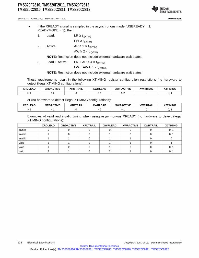
TMS320F2810, TMS320F2811, TMS320F2812TMS320C2810, TMS320C2811, TMS320C2812
SPRS174T –APRIL 2001–REVISED MAY 2012 www.ti.com
● If the XREADY signal is sampled in the asynchronous mode (USEREADY = 1,READYMODE = 1), then:
1. Lead: LR ≥ tc(XTIM)
LW ≥ tc(XTIM)
2. Active: AR ≥ 2 × tc(XTIM)
AW ≥ 2 × tc(XTIM)
NOTE: Restriction does not include external hardware wait states
3. Lead + Active: LR + AR ≥ 4 × tc(XTIM)
LW + AW ≥ 4 × tc(XTIM)
NOTE: Restriction does not include external hardware wait states
These requirements result in the following XTIMING register configuration restrictions (no hardware todetect illegal XTIMING configurations):
XRDLEAD XRDACTIVE XRDTRAIL XWRLEAD XWRACTIVE XWRTRAIL X2TIMING
≥ 1 ≥ 2 0 ≥ 1 ≥ 2 0 0, 1
or (no hardware to detect illegal XTIMING configurations):
XRDLEAD XRDACTIVE XRDTRAIL XWRLEAD XWRACTIVE XWRTRAIL X2TIMING
≥ 2 ≥ 1 0 ≥ 2 ≥ 1 0 0, 1
Examples of valid and invalid timing when using asynchronous XREADY (no hardware to detect illegalXTIMING configurations):
XRDLEAD XRDACTIVE XRDTRAIL XWRLEAD XWRACTIVE XWRTRAIL X2TIMING
Invalid 0 0 0 0 0 0 0, 1
Invalid 1 0 0 1 0 0 0, 1
Invalid 1 1 0 1 1 0 0
Valid 1 1 0 1 1 0 1
Valid 1 2 0 1 2 0 0, 1
Valid 2 1 0 2 1 0 0, 1
128 Electrical Specifications Copyright © 2001–2012, Texas Instruments Incorporated
Submit Documentation FeedbackProduct Folder Link(s): TMS320F2810 TMS320F2811 TMS320F2812 TMS320C2810 TMS320C2811 TMS320C2812
XTIMING0
XTIMING1
XTIMING2
XTIMING6
XTIMING7
XBANK
LEAD/ACTIVE/TRAIL
0
/2XTIMCLK1
(A)
1(A)
0
/2C28xCPU
XINTCNF2(CLKMODE)
XINTCNF2(XTIMCLK)
Default value after reset(A)
SYSCLKOUT
XINTCNF2(CLKOFF)
XCLKOUT1
0
0
TMS320F2810, TMS320F2811, TMS320F2812TMS320C2810, TMS320C2811, TMS320C2812
www.ti.com SPRS174T –APRIL 2001–REVISED MAY 2012
Unless otherwise specified, all XINTF timing is applicable for the clock configurations shown in Table 6-31.
Table 6-31. XINTF Clock Configurations
MODE SYSCLKOUT XTIMCLK XCLKOUT
1 SYSCLKOUT SYSCLKOUTExample: 150 MHz 150 MHz 150 MHz
2 SYSCLKOUT 1/2 SYSCLKOUTExample: 150 MHz 150 MHz 75 MHz
3 1/2 SYSCLKOUT 1/2 SYSCLKOUTExample: 150 MHz 75 MHz 75 MHz
4 1/2 SYSCLKOUT 1/4 SYSCLKOUTExample: 150 MHz 75 MHz 37.5 MHz
The relationship between SYSCLKOUT and XTIMCLK is shown in Figure 6-30.
Figure 6-30. Relationship Between XTIMCLK and SYSCLKOUT
Copyright © 2001–2012, Texas Instruments Incorporated Electrical Specifications 129Submit Documentation Feedback
Product Folder Link(s): TMS320F2810 TMS320F2811 TMS320F2812 TMS320C2810 TMS320C2811 TMS320C2812

TMS320F2810, TMS320F2811, TMS320F2812TMS320C2810, TMS320C2811, TMS320C2812
SPRS174T –APRIL 2001–REVISED MAY 2012 www.ti.com
6.23 XINTF Signal Alignment to XCLKOUT
For each XINTF access, the number of lead, active, and trail cycles is based on the internal clockXTIMCLK. Strobes such as XRD, XWE, and zone chip-select (XZCS) change state in relationship to therising edge of XTIMCLK. The external clock, XCLKOUT, can be configured to be either equal to or one-half the frequency of XTIMCLK.
For the case where XCLKOUT = XTIMCLK, all of the XINTF strobes will change state with respect to therising edge of XCLKOUT. For the case where XCLKOUT = one-half XTIMCLK, some strobes will changestate either on the rising edge of XCLKOUT or the falling edge of XCLKOUT. In the XINTF timing tables,the notation XCOHL is used to indicate that the parameter is with respect to either case; XCLKOUT risingedge (high) or XCLKOUT falling edge (low). If the parameter is always with respect to the rising edge ofXCLKOUT, the notation XCOH is used.
For the case where XCLKOUT = one-half XTIMCLK, the XCLKOUT edge with which the change will bealigned can be determined based on the number of XTIMCLK cycles from the start of the access to thepoint at which the signal changes. If this number of XTIMCLK cycles is even, the alignment will be withrespect to the rising edge of XCLKOUT. If this number is odd, then the signal will change with respect tothe falling edge of XCLKOUT. Examples include the following:• Strobes that change at the beginning of an access always align to the rising edge of XCLKOUT. This is
because all XINTF accesses begin with respect to the rising edge of XCLKOUT.
Examples: XZCSL Zone chip-select active-low
XRNWL XR/W active-low
• Strobes that change at the beginning of the active period will align to the rising edge of XCLKOUT ifthe total number of lead XTIMCLK cycles for the access is even. If the number of lead XTIMCLKcycles is odd, then the alignment will be with respect to the falling edge of XCLKOUT.
Examples: XRDL XRD active-low
XWEL XWE active-low
• Strobes that change at the beginning of the trail period will align to the rising edge of XCLKOUT if thetotal number of lead + active XTIMCLK cycles (including hardware waitstates) for the access is even. Ifthe number of lead + active XTIMCLK cycles (including hardware waitstates) is odd, then the alignmentwill be with respect to the falling edge of XCLKOUT.
Examples: XRDH XRD inactive-high
XWEH XWE inactive-high
• Strobes that change at the end of the access will align to the rising edge of XCLKOUT if the totalnumber of lead + active + trail XTIMCLK cycles (including hardware waitstates) is even. If the numberof lead + active + trail XTIMCLK cycles (including hardware waitstates) is odd, then the alignment willbe with respect to the falling edge of XCLKOUT.
Examples: XZCSH Zone chip-select inactive-high
XRNWH XR/W inactive-high
130 Electrical Specifications Copyright © 2001–2012, Texas Instruments Incorporated
Submit Documentation FeedbackProduct Folder Link(s): TMS320F2810 TMS320F2811 TMS320F2812 TMS320C2810 TMS320C2811 TMS320C2812

TMS320F2810, TMS320F2811, TMS320F2812TMS320C2810, TMS320C2811, TMS320C2812
www.ti.com SPRS174T –APRIL 2001–REVISED MAY 2012
6.24 External Interface Read Timing
Table 6-32. External Memory Interface Read Switching Characteristics
PARAMETER MIN MAX UNIT
td(XCOH-XZCSL) Delay time, XCLKOUT high to zone chip-select active-low 1 ns
td(XCOHL-XZCSH) Delay time, XCLKOUT high/low to zone chip-select inactive-high –2 3 ns
td(XCOH-XA) Delay time, XCLKOUT high to address valid 2 ns
td(XCOHL-XRDL) Delay time, XCLKOUT high/low to XRD active-low 1 ns
td(XCOHL-XRDH) Delay time, XCLKOUT high/low to XRD inactive-high –2 1 ns
th(XA)XZCSH Hold time, address valid after zone chip-select inactive-high (1) ns
th(XA)XRD Hold time, address valid after XRD inactive-high (1) ns
(1) During inactive cycles, the XINTF address bus will always hold the last address put out on the bus. This includes alignment cycles.
Table 6-33. External Memory Interface Read Timing Requirements
MIN MAX UNIT
ta(A) Access time, read data from address valid (LR + AR) – 14 (1) ns
ta(XRD) Access time, read data valid from XRD active-low AR – 12 (1) ns
tsu(XD)XRD Setup time, read data valid before XRD strobe inactive-high 12 ns
th(XD)XRD Hold time, read data valid after XRD inactive-high 0 ns
(1) LR = Lead period, read access. AR = Active period, read access. See Table 6-30.
Copyright © 2001–2012, Texas Instruments Incorporated Electrical Specifications 131Submit Documentation Feedback
Product Folder Link(s): TMS320F2810 TMS320F2811 TMS320F2812 TMS320C2810 TMS320C2811 TMS320C2812

DIN
td(XCOHL-XRDL)
td(XCOH-XA)
td(XCOH-XZCSL)
td(XCOHL-XRDH)
th(XD)XRD
td(XCOHL-XZCSH)
XCLKOUT = XTIMCLK
XCLKOUT = 1/2 XTIMCLK
XZCS0AND1 XZCS2XZCS6AND7
, ,
XA[0:18]
XRD
XWE
XR/W
XD[0:15]
tsu(XD)XRD
ta(A)
ta(XRD)
XREADY
LeadActive
Trail
TMS320F2810, TMS320F2811, TMS320F2812TMS320C2810, TMS320C2811, TMS320C2812
SPRS174T –APRIL 2001–REVISED MAY 2012 www.ti.com
A. All XINTF accesses (lead period) begin on the rising edge of XCLKOUT. When necessary, the device will insert analignment cycle before an access to meet this requirement.
B. During alignment cycles, all signals will transition to their inactive state.C. For USEREADY = 0, the external XREADY input signal is ignored.D. XA[0:18] will hold the last address put on the bus during inactive cycles, including alignment cycles.
Figure 6-31. Example Read Access
XTIMING register parameters used for this example:
XRDLEAD XRDACTIVE XRDTRAIL USEREADY X2TIMING XWRLEAD XWRACTIVE XWRTRAIL READYMODE
≥ 1 ≥ 0 ≥ 0 0 0 N/A (1) N/A (1) N/A (1) N/A (1)
(1) N/A = “Don’t care” for this example
132 Electrical Specifications Copyright © 2001–2012, Texas Instruments Incorporated
Submit Documentation FeedbackProduct Folder Link(s): TMS320F2810 TMS320F2811 TMS320F2812 TMS320C2810 TMS320C2811 TMS320C2812

LeadActive
Trail
td(XCOH-XZCSL)
td(XCOH-XA)
td(XCOHL-XWEL) td(XCOHL-XWEH)
td(XCOHL-XZCSH)
ten(XD)XWELth(XD)XWEH
tdis(XD)XRNW
XCLKOUT = XTIMCLK
XCLKOUT = 1/2 XTIMCLK
XZCS0AND1 XZCS2XZCS6AND7
, ,
XA[0:18]
XRD
XWE
XR/W
XD[0:15]
td(XCOH-XRNWL) td(XCOHL-XRNWH)
DOUT
XREADY
td(XWEL-XD)
TMS320F2810, TMS320F2811, TMS320F2812TMS320C2810, TMS320C2811, TMS320C2812
www.ti.com SPRS174T –APRIL 2001–REVISED MAY 2012
6.25 External Interface Write Timing
Table 6-34. External Memory Interface Write Switching Characteristics
PARAMETER MIN MAX UNIT
td(XCOH-XZCSL) Delay time, XCLKOUT high to zone chip-select active-low 1 ns
td(XCOHL-XZCSH) Delay time, XCLKOUT high or low to zone chip-select inactive-high –2 3 ns
td(XCOH-XA) Delay time, XCLKOUT high to address valid 2 ns
td(XCOHL-XWEL) Delay time, XCLKOUT high/low to XWE low 2 ns
td(XCOHL-XWEH) Delay time, XCLKOUT high/low to XWE high 2 ns
td(XCOH-XRNWL) Delay time, XCLKOUT high to XR/W low 1 ns
td(XCOHL-XRNWH) Delay time, XCLKOUT high/low to XR/W high –2 1 ns
ten(XD)XWEL Enable time, data bus driven from XWE low 0 ns
td(XWEL-XD) Delay time, data valid after XWE active-low 4 ns
th(XA)XZCSH Hold time, address valid after zone chip-select inactive-high (1) ns
th(XD)XWE Hold time, write data valid after XWE inactive-high TW – 2 (2) ns
tdis(XD)XRNW Maximum time for DSP to release the data bus after XR/W inactive-high 4 ns
(1) During inactive cycles, the XINTF address bus will always hold the last address put out on the bus. This includes alignment cycles.(2) TW = Trail period, write access. See Table 6-30.
A. All XINTF accesses (lead period) begin on the rising edge of XCLKOUT. When necessary, the device will insert analignment cycle before an access to meet this requirement.
B. During alignment cycles, all signals will transition to their inactive state.C. For USEREADY = 0, the external XREADY input signal is ignored.D. XA[0:18] will hold the last address put on the bus during inactive cycles, including alignment cycles.
Figure 6-32. Example Write Access
XTIMING register parameters used for this example:
XRDLEAD XRDACTIVE XRDTRAIL USEREADY X2TIMING XWRLEAD XWRACTIVE XWRTRAIL READYMODE
N/A (1) N/A (1) N/A (1) 0 0 ≥ 1 ≥ 0 ≥ 0 N/A (1)
(1) N/A = “Don’t care” for this example
Copyright © 2001–2012, Texas Instruments Incorporated Electrical Specifications 133Submit Documentation Feedback
Product Folder Link(s): TMS320F2810 TMS320F2811 TMS320F2812 TMS320C2810 TMS320C2811 TMS320C2812

TMS320F2810, TMS320F2811, TMS320F2812TMS320C2810, TMS320C2811, TMS320C2812
SPRS174T –APRIL 2001–REVISED MAY 2012 www.ti.com
6.26 External Interface Ready-on-Read Timing With One External Wait State
Table 6-35. External Memory Interface Read Switching Characteristics (Ready-on-Read, 1 Wait State)
PARAMETER MIN MAX UNIT
td(XCOH-XZCSL) Delay time, XCLKOUT high to zone chip-select active-low 1 ns
td(XCOHL-XZCSH) Delay time, XCLKOUT high/low to zone chip-select inactive-high –2 3 ns
td(XCOH-XA) Delay time, XCLKOUT high to address valid 2 ns
td(XCOHL-XRDL) Delay time, XCLKOUT high/low to XRD active-low 1 ns
td(XCOHL-XRDH) Delay time, XCLKOUT high/low to XRD inactive-high –2 1 ns
th(XA)XZCSH Hold time, address valid after zone chip-select inactive-high (1) ns
th(XA)XRD Hold time, address valid after XRD inactive-high (1) ns
(1) During inactive cycles, the XINTF address bus will always hold the last address put out on the bus. This includes alignment cycles.
Table 6-36. External Memory Interface Read Timing Requirements (Ready-on-Read, 1 Wait State)
MIN MAX UNIT
ta(A) Access time, read data from address valid (LR + AR) – 14 (1) ns
ta(XRD) Access time, read data valid from XRD active-low AR – 12 (1) ns
tsu(XD)XRD Setup time, read data valid before XRD strobe inactive-high 12 ns
th(XD)XRD Hold time, read data valid after XRD inactive-high 0 ns
(1) LR = Lead period, read access. AR = Active period, read access. See Table 6-30.
Table 6-37. Synchronous XREADY Timing Requirements (Ready-on-Read, 1 Wait State) (1)
MIN MAX UNIT
tsu(XRDYsynchL)XCOHL Setup time, XREADY (synchronous) low before XCLKOUT high/low 15 ns
th(XRDYsynchL) Hold time, XREADY (synchronous) low 12 ns
Earliest time XREADY (synchronous) can go high before the samplingte(XRDYsynchH) 3 nsXCLKOUT edge
tsu(XRDYsynchH)XCOHL Setup time, XREADY (synchronous) high before XCLKOUT high/low 15 ns
th(XRDYsynchH)XZCSH Hold time, XREADY (synchronous) held high after zone chip-select high 0 ns
(1) The first XREADY (synchronous) sample occurs with respect to E in Figure 6-33:E = (XRDLEAD + XRDACTIVE) tc(XTIM)When first sampled, if XREADY (synchronous) is found to be high, then the access will complete. If XREADY (synchronous) is found tobe low, it will be sampled again each tc(XTIM) until it is found to be high.For each sample (n), the setup time (D) with respect to the beginning of the access can be calculated as:D = (XRDLEAD + XRDACTIVE + n – 1) tc(XTIM) – tsu(XRDYsynchL)XCOHLwhere n is the sample number (n = 1, 2, 3, and so forth).
Table 6-38. Asynchronous XREADY Timing Requirements (Ready-on-Read, 1 Wait State) (1)
MIN MAX UNIT
tsu(XRDYAsynchL)XCOHL Setup time, XREADY (asynchronous) low before XCLKOUT high/low 11 ns
th(XRDYAsynchL) Hold time, XREADY (asynchronous) low 8 ns
Earliest time XREADY (asynchronous) can go high before the samplingte(XRDYAsynchH) 3 nsXCLKOUT edge
tsu(XRDYAsynchH)XCOHL Setup time, XREADY (asynchronous) high before XCLKOUT high/low 11 ns
th(XRDYAsynchH)XZCSH Hold time, XREADY (asynchronous) held high after zone chip-select high 0 ns
(1) The first XREADY (asynchronous) sample occurs with respect to E in Figure 6-34:E = (XRDLEAD + XRDACTIVE – 2) tc(XTIM)When first sampled, if XREADY (asynchronous) is found to be high, then the access will complete. If XREADY (asynchronous) is foundto be low, it will be sampled again each tc(XTIM) until it is found to be high.For each sample, setup time from the beginning of the access can be calculated as:D = (XRDLEAD + XRDACTIVE – 3 + n) tc(XTIM) – tsu(XRDYAsynchL)XCOHLwhere n is the sample number (n = 1, 2, 3, and so forth).
134 Electrical Specifications Copyright © 2001–2012, Texas Instruments Incorporated
Submit Documentation FeedbackProduct Folder Link(s): TMS320F2810 TMS320F2811 TMS320F2812 TMS320C2810 TMS320C2811 TMS320C2812

LeadActive
Trail
DIN
td(XCOH-XZCSL)
td(XCOH-XA)
td(XCOHL-XRDL)
td(XCOHL-XZCSH)
td(XCOHL-XRDH)
WS (Synch)
XCLKOUT = XTIMCLK
XCLKOUT = 1/2 XTIMCLK
XZCS0AND1 XZCS2XZCS6AND7
, ,
XA[0:18]
XRD
XWE
XR/W
XD[0:15]
XREADY(Synch)
th(XRDYsynchL)
tsu(XRDYsynchL)XCOHL
tsu(XD)XRD
ta(XRD)
ta(A)th(XD)XRD
th(XRDYsynchH)XZCSHtsu(XRDHsynchH)XCOHL
See Note (E)
= Don’t care. Signal can be high or low during this time.
Legend:
te(XRDYsynchH)
See Note (D)
See Notes (A) and (B)
See Note (C)
TMS320F2810, TMS320F2811, TMS320F2812TMS320C2810, TMS320C2811, TMS320C2812
www.ti.com SPRS174T –APRIL 2001–REVISED MAY 2012
A. All XINTF accesses (lead period) begin on the rising edge of XCLKOUT. When necessary, the device will insert analignment cycle before an access to meet this requirement.
B. During alignment cycles, all signals will transition to their inactive state.C. During inactive cycles, the XINTF address bus will always hold the last address put out on the bus. This includes
alignment cycles.D. For each sample, setup time from the beginning of the access (D) can be calculated as:
D = (XRDLEAD + XRDACTIVE + n – 1) tc(XTIM) – tsu(XRDYsynchL)XCOHL
E. Reference for the first sample is with respect to this pointE = (XRDLEAD + XRDACTIVE) tc(XTIM)where n is the sample number (n = 1, 2, 3, and so forth).
Figure 6-33. Example Read With Synchronous XREADY Access
XTIMING register parameters used for this example:
XRDLEAD XRDACTIVE XRDTRAIL USEREADY X2TIMING XWRLEAD XWRACTIVE XWRTRAIL READYMODE
0 = XREADY≥ 1 3 ≥ 1 1 0 N/A (1) N/A (1) N/A (1)(Synch)
(1) N/A = “Don’t care” for this example
Copyright © 2001–2012, Texas Instruments Incorporated Electrical Specifications 135Submit Documentation Feedback
Product Folder Link(s): TMS320F2810 TMS320F2811 TMS320F2812 TMS320C2810 TMS320C2811 TMS320C2812

tsu(XD)XRD
LeadActive
Trail
DIN
td(XCOH-XZCSL)
td(XCOH-XA)
td(XCOHL-XRDL)
td(XCOHL-XZCSH)
td(XCOHL-XRDH)
WS (Async)
XCLKOUT = XTIMCLK
XCLKOUT = 1/2 XTIMCLK
XZCS0AND1 XZCS2XZCS6AND7
, ,
XA[0:18]
XRD
XWE
XR/W
XD[0:15]
XREADY(Asynch)
tsu(XRDYasynchL)XCOHL
ta(A)
th(XD)XRD
th(XRDYasynchH)XZCSH
SeeNotes (A)and (B)
See Note (C)
tsu(XRDYasynchH)XCOHL
See Note (D)
= Don’t care. Signal can be high or low during this time.
Legend:
te(XRDYasynchH)
See Note (E)
ta(XRD)
th(XRDYasynchL)
TMS320F2810, TMS320F2811, TMS320F2812TMS320C2810, TMS320C2811, TMS320C2812
SPRS174T –APRIL 2001–REVISED MAY 2012 www.ti.com
A. All XINTF accesses (lead period) begin on the rising edge of XCLKOUT. When necessary, the device will insert analignment cycle before an access to meet this requirement.
B. During alignment cycles, all signals will transition to their inactive state.C. During inactive cycles, the XINTF address bus will always hold the last address put out on the bus. This includes
alignment cycles.D. For each sample, setup time from the beginning of the access can be calculated as:
D = (XRDLEAD + XRDACTIVE – 3 + n) tc(XTIM) – tsu(XRDYAsynchL)XCOHLwhere n is the sample number (n = 1, 2, 3, and so forth).
E. Reference for the first sample is with respect to this point:E = (XRDLEAD + XRDACTIVE – 2) tc(XTIM)
Figure 6-34. Example Read With Asynchronous XREADY Access
XTIMING register parameters used for this example:
XRDLEAD XRDACTIVE XRDTRAIL USEREADY X2TIMING XWRLEAD XWRACTIVE XWRTRAIL READYMODE
1 = XREADY≥ 1 3 ≥ 1 1 0 N/A (1) N/A (1) N/A (1)(Async)
(1) N/A = “Don’t care” for this example
136 Electrical Specifications Copyright © 2001–2012, Texas Instruments Incorporated
Submit Documentation FeedbackProduct Folder Link(s): TMS320F2810 TMS320F2811 TMS320F2812 TMS320C2810 TMS320C2811 TMS320C2812

TMS320F2810, TMS320F2811, TMS320F2812TMS320C2810, TMS320C2811, TMS320C2812
www.ti.com SPRS174T –APRIL 2001–REVISED MAY 2012
6.27 External Interface Ready-on-Write Timing With One External Wait State
Table 6-39. External Memory Interface Write Switching Characteristics (Ready-on-Write, 1 Wait State)
PARAMETER MIN MAX UNIT
td(XCOH-XZCSL) Delay time, XCLKOUT high to zone chip-select active-low 1 ns
td(XCOHL-XZCSH) Delay time, XCLKOUT high or low to zone chip-select inactive-high –2 3 ns
td(XCOH-XA) Delay time, XCLKOUT high to address valid 2 ns
td(XCOHL-XWEL) Delay time, XCLKOUT high/low to XWE low 2 ns
td(XCOHL-XWEH) Delay time, XCLKOUT high/low to XWE high 2 ns
td(XCOH-XRNWL) Delay time, XCLKOUT high to XR/W low 1 ns
td(XCOHL-XRNWH) Delay time, XCLKOUT high/low to XR/W high –2 1 ns
ten(XD)XWEL Enable time, data bus driven from XWE low 0 ns
td(XWEL-XD) Delay time, data valid after XWE active-low 4 ns
th(XA)XZCSH Hold time, address valid after zone chip-select inactive-high (1) ns
th(XD)XWE Hold time, write data valid after XWE inactive-high TW – 2 (2) ns
tdis(XD)XRNW Maximum time for DSP to release the data bus after XR/W inactive-high 4 ns
(1) During inactive cycles, the XINTF address bus will always hold the last address put out on the bus. This includes alignment cycles.(2) TW = trail period, write access. See Table 6-30.
Table 6-40. Synchronous XREADY Timing Requirements (Ready-on-Write, 1 Wait State) (1)
MIN MAX UNIT
tsu(XRDYsynchL)XCOHL Setup time, XREADY (synchronous) low before XCLKOUT high/low 15 ns
th(XRDYsynchL) Hold time, XREADY (synchronous) low 12 ns
Earliest time XREADY (synchronous) can go high before the samplingte(XRDYsynchH) 3 nsXCLKOUT edge
tsu(XRDYsynchH)XCOHL Setup time, XREADY (synchronous) high before XCLKOUT high/low 15 ns
th(XRDYsynchH)XZCSH Hold time, XREADY (synchronous) held high after zone chip-select high 0 ns
(1) The first XREADY (synchronous) sample occurs with respect to E in Figure 6-35:E = (XWRLEAD + XWRACTIVE) tc(XTIM)When first sampled, if XREADY (synchronous) is found to be high, then the access will complete. If XREADY (synchronous) is found tobe low, it will be sampled again each tc(XTIM) until it is found to be high.For each sample, setup time from the beginning of the access can be calculated as:D = (XWRLEAD + XWRACTIVE + n – 1) tc(XTIM) – tsu(XRDYsynchL)XCOHLwhere n is the sample number (n = 1, 2, 3, and so forth).
Table 6-41. Asynchronous XREADY Timing Requirements (Ready-on-Write, 1 Wait State) (1)
MIN MAX UNIT
tsu(XRDYasynchL)XCOHL Setup time, XREADY (asynchronous) low before XCLKOUT high/low 11 ns
th(XRDYasynchL) Hold time, XREADY (asynchronous) low 8 ns
Earliest time XREADY (asynchronous) can go high before the samplingte(XRDYasynchH) 3 nsXCLKOUT edge
tsu(XRDYasynchH)XCOHL Setup time, XREADY (asynchronous) high before XCLKOUT high/low 11 ns
th(XRDYasynchH)XZCSH Hold time, XREADY (asynchronous) held high after zone chip-select high 0 ns
(1) The first XREADY (synchronous) sample occurs with respect to E in Figure 6-36:E = (XWRLEAD + XWRACTIVE – 2) tc(XTIM)When first sampled, if XREADY (asynchronous) is found to be high, then the access will complete. If XREADY (asynchronous) is foundto be low, it will be sampled again each tc(XTIM) until it is found to be high.For each sample, setup time from the beginning of the access can be calculated as:D = (XWRLEAD + XWRACTIVE – 3 + n) tc(XTIM) – tsu(XRDYasynchL)XCOHLwhere n is the sample number (n = 1, 2, 3, and so forth).
Copyright © 2001–2012, Texas Instruments Incorporated Electrical Specifications 137Submit Documentation Feedback
Product Folder Link(s): TMS320F2810 TMS320F2811 TMS320F2812 TMS320C2810 TMS320C2811 TMS320C2812

Lead 1Active
Trail
XCLKOUT = XTIMCLK
XCLKOUT = 1/2 XTIMCLK
XA[0:18]
XD[0:15]
XREADY(Synch)
td(XCOHL-XWEL)td(XCOHL-XWEH)
td(XCOHL-XZCSH)
td(XCOH-XA)
WS (Synch)
XZCS0AND1 XZCS2XZCS6AND7
, ,
XRD
XWE
XR/W
td(XCOH-XZCSL)
td(XCOH-XRNWL) td(XCOHL-XRNWH)
ten(XD)XWELth(XD)XWEH
tsu(XRDHsynchH)XCOHL
tsu(XRDYsynchL)XCOHL
DOUT
td(XWEL-XD)tdis(XD)XRNW
th(XRDYsynchL)
th(XRDYsynchH)XZCSH
See Note (E)
See Note (D)
SeeNotes (A)and (B) See Note (C)
= Don’t care. Signal can be high or low during this time.
Legend:
te(XRDYsynchH)
TMS320F2810, TMS320F2811, TMS320F2812TMS320C2810, TMS320C2811, TMS320C2812
SPRS174T –APRIL 2001–REVISED MAY 2012 www.ti.com
A. All XINTF accesses (lead period) begin on the rising edge of XCLKOUT. When necessary, the device will insert analignment cycle before an access to meet this requirement.
B. During alignment cycles, all signals will transition to their inactive state.C. During inactive cycles, the XINTF address bus will always hold the last address put out on the bus. This includes
alignment cycles.D. For each sample, setup time from the beginning of the access can be calculated as:
D = (XWRLEAD + XWRACTIVE + n – 1) tc(XTIM) – tsu(XRDYsynchL)XCOHLwhere n is the sample number (n = 1, 2, 3 and so forth).
E. Reference for the first sample is with respect to this pointE = (XWRLEAD + XWRACTIVE) tc(XTIM)
Figure 6-35. Write With Synchronous XREADY Access
XTIMING register parameters used for this example:
XRDLEAD XRDACTIVE XRDTRAIL USEREADY X2TIMING XWRLEAD XWRACTIVE XWRTRAIL READYMODE
0 = XREADYN/A (1) N/A (1) N/A (1) 1 0 ≥ 1 3 ≥ 1 (Synch)
(1) N/A = “Don’t care” for this example
138 Electrical Specifications Copyright © 2001–2012, Texas Instruments Incorporated
Submit Documentation FeedbackProduct Folder Link(s): TMS320F2810 TMS320F2811 TMS320F2812 TMS320C2810 TMS320C2811 TMS320C2812

Lead 1Active Trail
XCLKOUT = XTIMCLK
XCLKOUT = 1/2 XTIMCLK
XA[0:18]
XD[0:15]
td(XCOHL-XWEH)
td(XCOHL-XZCSH)
td(XCOH-XA)
WS (Async)
XZCS0AND1 XZCS2XZCS6AND7
, ,
XRD
XWE
XR/W
td(XCOH-XZCSL)
td(XCOH-XRNWL)td(XCOHL-XRNWH)
ten(XD)XWEL
th(XD)XWEH
th(XRDYasynchL)
DOUT
tdis(XD)XRNW
th(XRDYasynchH)XZCSH
See Note (E)
See Note (D)
tsu(XRDYasynchL)XCOHL
tsu(XRDYasynchH)XCOHL
td(XWEL-XD)
td(XCOHL-XWEL)
SeeNotes (A)and (B)
See Note (C)
= Don’t care. Signal can be high or low during this time.
Legend:
te(XRDYasynchH)
XREADY(Asynch)
TMS320F2810, TMS320F2811, TMS320F2812TMS320C2810, TMS320C2811, TMS320C2812
www.ti.com SPRS174T –APRIL 2001–REVISED MAY 2012
A. All XINTF accesses (lead period) begin on the rising edge of XCLKOUT. When necessary, the device will insert analignment cycle before an access to meet this requirement.
B. During alignment cycles, all signals will transition to their inactive state.C. During inactive cycles, the XINTF address bus will always hold the last address put out on the bus. This includes
alignment cycles.D. For each sample, setup time from the beginning of the access can be calculated as:
D = (XWRLEAD + XWRACTIVE – 3 + n) tc(XTIM) – tsu(XRDYasynchL)XCOHLwhere n is the sample number (n = 1, 2, 3 and so forth).
E. Reference for the first sample is with respect to this pointE = (XWRLEAD + XWRACTIVE – 2) tc(XTIM)
Figure 6-36. Write With Asynchronous XREADY Access
XTIMING register parameters used for this example:
XRDLEAD XRDACTIVE XRDTRAIL USEREADY X2TIMING XWRLEAD XWRACTIVE XWRTRAIL READYMODE
1 = XREADYN/A (1) N/A (1) N/A (1) 1 0 ≥ 1 3 ≥ 1 (Async)
(1) N/A = “Don’t care” for this example
Copyright © 2001–2012, Texas Instruments Incorporated Electrical Specifications 139Submit Documentation Feedback
Product Folder Link(s): TMS320F2810 TMS320F2811 TMS320F2812 TMS320C2810 TMS320C2811 TMS320C2812

TMS320F2810, TMS320F2811, TMS320F2812TMS320C2810, TMS320C2811, TMS320C2812
SPRS174T –APRIL 2001–REVISED MAY 2012 www.ti.com
6.28 XHOLD and XHOLDA
If the HOLD mode bit is set while XHOLD and XHOLDA are both low (external bus accesses granted), theXHOLDA signal is forced high (at the end of the current cycle) and the external interface is taken out ofhigh-impedance mode.
On a reset (XRS), the HOLD mode bit is set to 0. If the XHOLD signal is active low on a system reset, thebus and all signal strobes must be in high-impedance mode, and the XHOLDA signal is also driven activelow.
When HOLD mode is enabled and XHOLDA is active-low (external bus grant active), the CPU can stillexecute code from internal memory. If an access is made to the external interface, the CPU is stalled untilthe XHOLD signal is removed.
An external DMA request, when granted, places the following signals in a high-impedance mode:
XA[18:0] XZCS0AND1
XD[15:0] XZCS2
XWE, XRD XZCS6AND7
XR/W
All other signals not listed in this group remain in their default or functional operational modes during thesesignal events.
140 Electrical Specifications Copyright © 2001–2012, Texas Instruments Incorporated
Submit Documentation FeedbackProduct Folder Link(s): TMS320F2810 TMS320F2811 TMS320F2812 TMS320C2810 TMS320C2811 TMS320C2812

XCLKOUT(/1 Mode)
XHOLD
XR/ ,,,
WXZCS0AND1
XZCS2XZCS6AND7
XD[15:0] Valid
XHOLDA
td(HL-Hiz)
td(HH-HAH)
High-Impedance
XA[18:0] Valid ValidHigh-Impedance
td(HH-BV)td(HL-HAL)
See Note (A) See Note (B)
TMS320F2810, TMS320F2811, TMS320F2812TMS320C2810, TMS320C2811, TMS320C2812
www.ti.com SPRS174T –APRIL 2001–REVISED MAY 2012
6.29 XHOLD/XHOLDA Timing
Table 6-42. XHOLD/XHOLDA Timing Requirements (XCLKOUT = XTIMCLK) (1) (2)
MIN MAX UNIT
td(HL-HiZ) Delay time, XHOLD low to Hi-Z on all Address, Data, and Control 4tc(XTIM) ns
td(HL-HAL) Delay time, XHOLD low to XHOLDA low 5tc(XTIM) ns
td(HH-HAH) Delay time, XHOLD high to XHOLDA high 3tc(XTIM) ns
td(HH-BV) Delay time, XHOLD high to Bus valid 4tc(XTIM) ns
(1) When a low signal is detected on XHOLD, all pending XINTF accesses will be completed before the bus is placed in a high-impedancestate.
(2) The state of XHOLD is latched on the rising edge of XTIMCLK.
A. All pending XINTF accesses are completed.B. Normal XINTF operation resumes.
Figure 6-37. External Interface Hold Waveform
Copyright © 2001–2012, Texas Instruments Incorporated Electrical Specifications 141Submit Documentation Feedback
Product Folder Link(s): TMS320F2810 TMS320F2811 TMS320F2812 TMS320C2810 TMS320C2811 TMS320C2812

XCLKOUT(1/2 XTIMCLK)
XHOLD
XR/ ,,,
WXZCS0AND1
XZCS2XZCS6AND7
XD[15:0] Valid
XHOLDAtd(HL-HiZ)
td(HH-HAH)
High-Impedance
High-Impedance
High-ImpedanceXA[18:0] Valid Valid
td(HH-BV)
td(HL-HAL)
See Note (A) See Note (B)
TMS320F2810, TMS320F2811, TMS320F2812TMS320C2810, TMS320C2811, TMS320C2812
SPRS174T –APRIL 2001–REVISED MAY 2012 www.ti.com
Table 6-43. XHOLD/XHOLDA Timing Requirements (XCLKOUT = 1/2 XTIMCLK) (1) (2) (3)
MIN MAX UNIT
td(HL-HiZ) Delay time, XHOLD low to Hi-Z on all Address, Data, and Control 4tc(XTIM) + tc(XCO) ns
td(HL-HAL) Delay time, XHOLD low to XHOLDA low 4tc(XTIM) + 2tc(XCO) ns
td(HH-HAH) Delay time, XHOLD high to XHOLDA high 4tc(XTIM) ns
td(HH-BV) Delay time, XHOLD high to Bus valid 6tc(XTIM) ns
(1) When a low signal is detected on XHOLD, all pending XINTF accesses will be completed before the bus is placed in a high-impedancestate.
(2) The state of XHOLD is latched on the rising edge of XTIMCLK.(3) After the XHOLD is detected low or high, all bus transitions and XHOLDA transitions will occur with respect to the rising edge of
XCLKOUT. Thus, for this mode where XCLKOUT = 1/2 XTIMCLK, the transitions can occur up to 1 XTIMCLK cycle earlier than themaximum value specified.
A. All pending XINTF accesses are completed.B. Normal XINTF operation resumes.
Figure 6-38. XHOLD/XHOLDA Timing Requirements (XCLKOUT = 1/2 XTIMCLK)
142 Electrical Specifications Copyright © 2001–2012, Texas Instruments Incorporated
Submit Documentation FeedbackProduct Folder Link(s): TMS320F2810 TMS320F2811 TMS320F2812 TMS320C2810 TMS320C2811 TMS320C2812

TMS320F2810, TMS320F2811, TMS320F2812TMS320C2810, TMS320C2811, TMS320C2812
www.ti.com SPRS174T –APRIL 2001–REVISED MAY 2012
6.30 On-Chip Analog-to-Digital Converter
6.30.1 ADC Absolute Maximum Ratings
Unless otherwise noted, the list of absolute maximum ratings are specified over operating conditions.Stresses beyond those listed under Absolute Maximum Ratings may cause permanent damage to thedevice. These are stress ratings only. Exposure to absolute-maximum-rated conditions for extendedperiods may affect device reliability.
Supply voltage range (VSSA1/VSSA2 to VDDA1/VDDA2/AVDDREFBG) –0.3 V to 4.6 V
Supply voltage range (VSS1 to VDD1) –0.3 V to 2.5 V
Analog Input (ADCIN) Clamp Current, total (max) ±20 mA (1)
(1) The analog inputs have an internal clamping circuit that clamps the voltage to a diode drop above VDDA or below VSS. The continuousclamp current per pin is ±2 mA.
Copyright © 2001–2012, Texas Instruments Incorporated Electrical Specifications 143Submit Documentation Feedback
Product Folder Link(s): TMS320F2810 TMS320F2811 TMS320F2812 TMS320C2810 TMS320C2811 TMS320C2812

TMS320F2810, TMS320F2811, TMS320F2812TMS320C2810, TMS320C2811, TMS320C2812
SPRS174T –APRIL 2001–REVISED MAY 2012 www.ti.com
6.30.2 ADC Electrical Characteristics Over Recommended Operating Conditions
Table 6-44. DC Specifications (1)
PARAMETER MIN TYP MAX UNIT
Resolution 12 Bits
1 kHzADC clock (2)
25 MHz
ACCURACY
INL (Integral nonlinearity) (3) 1–18.75 MHz ADC clock ±1.5 LSB
DNL (Differential nonlinearity) (3) 1–18.75 MHz ADC clock ±1 LSB
Offset error (4) –80 80 LSB
F281x –200 200Overall gain error with internal reference (5) LSB
C281x –80 80
Overall gain error with external reference (6) If ADCREFP – ADCREFM = 1 V ± 0.1% –50 50 LSB
Channel-to-channel offset variation ±8 LSB
Channel-to-channel Gain variation ±8 LSB
ANALOG INPUT
Analog input voltage (ADCINx to ADCLO) (7) 0 3 V
ADCLO –5 0 5 mV
Input capacitance 10 pF
Input leakage current 3 ±5 µA
INTERNAL VOLTAGE REFERENCE (5)
Accuracy, ADCVREFP 1.9 2 2.1 V
Accuracy, ADCVREFM 0.95 1 1.05 V
Voltage difference, ADCREFP – ADCREFM 1 V
Temperature coefficient 50 PPM/°C
Reference noise 100 µV
EXTERNAL VOLTAGE REFERENCE (6)
Accuracy, ADCVREFP 1.9 2 2.1 V
Accuracy, ADCVREFM 0.95 1 1.05 V
Input voltage difference, ADCREFP – ADCREFM 0.99 1 1.01 V
(1) Tested at 12.5-MHz ADCCLK.(2) If SYSCLKOUT ≤ 25 MHz, ADC clock ≤ SYSCLKOUT/2.(3) The INL degrades for frequencies beyond 18.75 MHz–25 MHz. Applications that require these sampling rates should use a 20K resistor
as bias resistor on the ADCRESEXT pin. This improves overall linearity and typical current drawn by the ADC will be a few mA morethan 24.9-kΩ bias. The ADC module in C281x devices can operate at 24.9k bias on ADCRESEXT pin for the full range 1–25 MHz.
(4) 1 LSB has the weighted value of 3.0/4096 = 0.732 mV.(5) A single internal band gap reference (±5% accuracy) sources both ADCREFP and ADCREFM signals, and hence, these voltages track
together. The ADC converter uses the difference between these two as its reference. The total gain error will be the combination of thegain error shown here and the voltage reference accuracy (ADCREFP – ADCREFM). A software-based calibration procedure isrecommended for better accuracy. See the F2810, F2811, and F2812 ADC Calibration Application Report (literature number SPRA989)and Section 5.2, Documentation Support, for relevant documents.
(6) In this mode, the accuracy of external reference is critical for overall gain. The voltage difference (ADCREFP – ADCREFM) willdetermine the overall accuracy.
(7) Voltages above VDDA + 0.3 V or below VSS – 0.3 V applied to an analog input pin may temporarily affect the conversion of another pin.To avoid this, the analog inputs should be kept within these limits.
144 Electrical Specifications Copyright © 2001–2012, Texas Instruments Incorporated
Submit Documentation FeedbackProduct Folder Link(s): TMS320F2810 TMS320F2811 TMS320F2812 TMS320C2810 TMS320C2811 TMS320C2812

ac
Rs ADCIN0
C
10 pFp C
1.25 pFh
Switch
Typical Values of the Input Circuit Components:
Switch Resistance (R ): 1 kon W
1 kW
Sampling Capacitor (C ): 1.25 pFh
Parasitic Capacitance (C ): 10 pFp
Source Resistance (R ): 50s W
28x DSP
SourceSignal
Ron
TMS320F2810, TMS320F2811, TMS320F2812TMS320C2810, TMS320C2811, TMS320C2812
www.ti.com SPRS174T –APRIL 2001–REVISED MAY 2012
Table 6-45. AC Specifications
PARAMETER MIN TYP MAX UNIT
SINAD Signal-to-noise ratio + distortion 62 dB
SNR Signal-to-noise ratio 62 dB
THD (100 kHz) Total harmonic distortion –68 dB
ENOB (SNR) Effective number of bits 10.1 Bits
SFDR Spurious free dynamic range 69 dB
6.30.3 Current Consumption for Different ADC Configurations
Table 6-46. Current Consumption for Different ADC Configurations (at 25-MHz ADCCLK) (1)
IDDA (TYP) (2) IDDAIO (TYP) IDD1 (TYP) ADC OPERATING MODE/CONDITIONS
Mode A (Operational Mode):40 mA 1 µA 0.5 mA • BG and REF enabled
• PWD disabled
Mode B:• ADC clock enabled
7 mA 0 5 µA• BG and REF enabled• PWD enabled
Mode C:• ADC clock enabled
1 µA 0 5 µA• BG and REF disabled• PWD enabled
Mode D:• ADC clock disabled
1 µA 0 0• BG and REF disabled• PWD enabled
(1) Test Conditions:• SYSCLKOUT = 150 MHz• ADC module clock = 25 MHz• ADC performing a continuous conversion of all 16 channels in Mode A
(2) IDDA – includes current into VDDA1/VDDA2 and AVDDREFBG
Figure 6-39. ADC Analog Input Impedance Model
Copyright © 2001–2012, Texas Instruments Incorporated Electrical Specifications 145Submit Documentation Feedback
Product Folder Link(s): TMS320F2810 TMS320F2811 TMS320F2812 TMS320C2810 TMS320C2811 TMS320C2812

ADC Power Up Delay ADC Ready for Conversions
PWDNBG
PWDNREF
PWDNADC
Request forADC Conversion
td(BGR)
td(PWD)
TMS320F2810, TMS320F2811, TMS320F2812TMS320C2810, TMS320C2811, TMS320C2812
SPRS174T –APRIL 2001–REVISED MAY 2012 www.ti.com
6.30.4 ADC Power-Up Control Bit Timing
Figure 6-40. ADC Power-Up Control Bit Timing
Table 6-47. ADC Power-Up Delays (1)
MIN TYP MAX UNIT
Delay time for band gap reference to be stable. Bits 7 and 6 of the ADCTRL3td(BGR) register (ADCBGRFDN1/0) are to be set to 1 before the ADCPWDN bit is 7 8 10 ms
enabled.
20 50 µsDelay time for power-down control to be stable. Bit 5 of the ADCTRL3 registertd(PWD) (ADCPWDN) is to be set to 1 before any ADC conversions are initiated. 1 ms
(1) These delays are necessary and recommended to make the ADC analog reference circuit stable before conversions are initiated. Ifconversions are started without these delays, the ADC results will show a higher gain. For power down, all three bits can be cleared atthe same time.
6.30.5 Detailed Description
6.30.5.1 Reference Voltage
The on-chip ADC has a built-in reference, which provides the reference voltages for the ADC. ADCVREFPis set to 2.0 V and ADCVREFM is set to 1.0 V.
6.30.5.2 Analog Inputs
The on-chip ADC consists of 16 analog inputs, which are sampled either one at a time or two channels ata time. These inputs are software-selectable.
6.30.5.3 Converter
The on-chip ADC uses a 12-bit four-stage pipeline architecture, which achieves a high sample rate withlow power consumption.
6.30.5.4 Conversion Modes
The conversion can be performed in two different conversion modes:• Sequential sampling mode (SMODE = 0)• Simultaneous sampling mode (SMODE = 1)
146 Electrical Specifications Copyright © 2001–2012, Texas Instruments Incorporated
Submit Documentation FeedbackProduct Folder Link(s): TMS320F2810 TMS320F2811 TMS320F2812 TMS320C2810 TMS320C2811 TMS320C2812

Analog Input onChannel Ax or Bx
ADC Clock
Sample and HoldSH Pulse
SMODE Bit
tdschx_n
tdschx_n+1
Sample n
Sample n+1
Sample n+2
tSH
ADC Event Trigger from EVor Other Sources
td(SH)
TMS320F2810, TMS320F2811, TMS320F2812TMS320C2810, TMS320C2811, TMS320C2812
www.ti.com SPRS174T –APRIL 2001–REVISED MAY 2012
6.30.6 Sequential Sampling Mode (Single-Channel) (SMODE = 0)
In sequential sampling mode, the ADC can continuously convert input signals on any of the channels (Axto Bx). The ADC can start conversions on event triggers from the Event Managers (EVA/EVB), softwaretrigger, or from an external ADCSOC signal. If the SMODE bit is 0, the ADC will do conversions on theselected channel on every Sample/Hold pulse. The conversion time and latency of the Result registerupdate are explained below. The ADC interrupt flags are set a few SYSCLKOUT cycles after the Resultregister update. The selected channels will be sampled at every falling edge of the Sample/Hold pulse.The Sample/Hold pulse width can be programmed to be 1 ADC clock wide (minimum) or 16 ADC clockswide (maximum).
Figure 6-41. Sequential Sampling Mode (Single-Channel) Timing
Table 6-48. Sequential Sampling Mode Timing
AT 25-MHzSAMPLE n SAMPLE n + 1 ADC CLOCK, REMARKS
tc(ADCCLK) = 40 ns
Delay time from eventtd(SH) 2.5tc(ADCCLK)trigger to sampling
Sample/ Acqps value = 0–15tSH Hold width/ (1 + Acqps) * tc(ADCCLK) 40 ns with Acqps = 0 ADCTRL1[8:11]Acquisition width
Delay time for firsttd(schx_n) result to appear in the 4tc(ADCCLK) 160 ns
Result register
Delay time forsuccessive results totd(schx_n+1) (2 + Acqps) * tc(ADCCLK) 80 nsappear in the Resultregister
Copyright © 2001–2012, Texas Instruments Incorporated Electrical Specifications 147Submit Documentation Feedback
Product Folder Link(s): TMS320F2810 TMS320F2811 TMS320F2812 TMS320C2810 TMS320C2811 TMS320C2812

Analog Input onChannel Ax
Analog Input onChannel Bv
ADC Clock
Sample and HoldSH Pulse
tSH
tdschA0_n
tdschB0_n
tdschB0_n+1
Sample nSample n+1 Sample n+2
tdschA0_n+1td(SH)
ADC Event Trigger from EVor Other Sources
SMODE Bit
TMS320F2810, TMS320F2811, TMS320F2812TMS320C2810, TMS320C2811, TMS320C2812
SPRS174T –APRIL 2001–REVISED MAY 2012 www.ti.com
6.30.7 Simultaneous Sampling Mode (Dual-Channel) (SMODE = 1)
In simultaneous mode, the ADC can continuously convert input signals on any one pair of channels(A0/B0 to A7/B7). The ADC can start conversions on event triggers from the Event Managers (EVA/EVB),software trigger, or from an external ADCSOC signal. If the SMODE bit is 1, the ADC will do conversionson two selected channels on every Sample/Hold pulse. The conversion time and latency of the Resultregister update are explained below. The ADC interrupt flags are set a few SYSCLKOUT cycles after theResult register update. The selected channels will be sampled simultaneously at the falling edge of theSample/Hold pulse. The Sample/Hold pulse width can be programmed to be 1 ADC clock wide (minimum)or 16 ADC clocks wide (maximum).
NOTEIn Simultaneous Mode, the ADCIN channel pair select has to be A0/B0, A1/B1, ..., A7/B7,and not in other combinations (such as A1/B3, and so forth).
Figure 6-42. Simultaneous Sampling Mode Timing
Table 6-49. Simultaneous Sampling Mode Timing
AT 25-MHzSAMPLE n SAMPLE n + 1 ADC CLOCK, REMARKS
tc(ADCCLK) = 40 ns
Delay time from eventtd(SH) 2.5tc(ADCCLK)trigger to sampling
Sample/Hold width/ Acqps value = 0–15tSH (1 + Acqps) * tc(ADCCLK) 40 ns with Acqps = 0Acquisition Width ADCTRL1[8:11]
Delay time for firsttd(schA0_n) result to appear in 4tc(ADCCLK) 160 ns
Result register
Delay time for firsttd(schB0_n) result to appear in 5tc(ADCCLK) 200 ns
Result register
Delay time forsuccessive results totd(schA0_n+1) (3 + Acqps) * tc(ADCCLK) 120 nsappear in Resultregister
Delay time forsuccessive results totd(schB0_n+1) (3 + Acqps) * tc(ADCCLK) 120 nsappear in Resultregister
148 Electrical Specifications Copyright © 2001–2012, Texas Instruments Incorporated
Submit Documentation FeedbackProduct Folder Link(s): TMS320F2810 TMS320F2811 TMS320F2812 TMS320C2810 TMS320C2811 TMS320C2812

6.02
1.76)(SINADN
-=
TMS320F2810, TMS320F2811, TMS320F2812TMS320C2810, TMS320C2811, TMS320C2812
www.ti.com SPRS174T –APRIL 2001–REVISED MAY 2012
6.30.8 Definitions of Specifications and Terminology
Integral Nonlinearity
Integral nonlinearity refers to the deviation of each individual code from a line drawn from zero through fullscale. The point used as zero occurs 1/2 LSB before the first code transition. The full-scale point isdefined as level 1/2 LSB beyond the last code transition. The deviation is measured from the center ofeach particular code to the true straight line between these two points.
Differential Nonlinearity
An ideal ADC exhibits code transitions that are exactly 1 LSB apart. DNL is the deviation from this idealvalue. A differential nonlinearity error of less than ±1 LSB ensures no missing codes.
Zero Offset
The major carry transition should occur when the analog input is at zero volt. Zero error is defined as thedeviation of the actual transition from that point.
Gain Error
The first code transition should occur at an analog value 1/2 LSB above negative full scale. The lasttransition should occur at an analog value 1 1/2 LSB below the nominal full scale. Gain error is thedeviation of the actual difference between first and last code transitions and the ideal difference betweenfirst and last code transitions.
Signal-to-Noise Ratio + Distortion (SINAD)
SINAD is the ratio of the rms value of the measured input signal to the rms sum of all other spectralcomponents below the Nyquist frequency, including harmonics but excluding dc. The value for SINAD isexpressed in decibels.
Effective Number of Bits (ENOB)
For a sine wave, SINAD can be expressed in terms of the number of bits. Using the following formula,
it is possible to get a measure of performance expressed as N, the effective number of bits. Thus,effective number of bits for a device for sine wave inputs at a given input frequency can be calculateddirectly from its measured SINAD.
Total Harmonic Distortion (THD)
THD is the ratio of the rms sum of the first six harmonic components to the rms value of the measuredinput signal and is expressed as a percentage or in decibels.
Spurious Free Dynamic Range (SFDR)
SFDR is the difference in dB between the rms amplitude of the input signal and the peak spurious signal.
Copyright © 2001–2012, Texas Instruments Incorporated Electrical Specifications 149Submit Documentation Feedback
Product Folder Link(s): TMS320F2810 TMS320F2811 TMS320F2812 TMS320C2810 TMS320C2811 TMS320C2812

TMS320F2810, TMS320F2811, TMS320F2812TMS320C2810, TMS320C2811, TMS320C2812
SPRS174T –APRIL 2001–REVISED MAY 2012 www.ti.com
6.31 Multichannel Buffered Serial Port (McBSP) Timing
6.31.1 McBSP Transmit and Receive Timing
Table 6-50. McBSP Timing Requirements (1) (2)
NO. MIN MAX UNIT
1 kHzMcBSP module clock (CLKG, CLKX, CLKR) range
20 (3) MHz
50 nsMcBSP module cycle time (CLKG, CLKX, CLKR) range
1 ms
M11 tc(CKRX) Cycle time, CLKR/X CLKR/X ext 2P ns
M12 tw(CKRX) Pulse duration, CLKR/X high or CLKR/X low CLKR/X ext P – 7 ns
M13 tr(CKRX) Rise time, CLKR/X CLKR/X ext 7 ns
M14 tf(CKRX) Fall time, CLKR/X CLKR/X ext 7 ns
CLKR int 18M15 tsu(FRH-CKRL) Setup time, external FSR high before CLKR low ns
CLKR ext 2
CLKR int 0M16 th(CKRL-FRH) Hold time, external FSR high after CLKR low ns
CLKR ext 6
CLKR int 18M17 tsu(DRV-CKRL) Setup time, DR valid before CLKR low ns
CLKR ext 2
CLKR int 0M18 th(CKRL-DRV) Hold time, DR valid after CLKR low ns
CLKR ext 6
CLKX int 18M19 tsu(FXH-CKXL) Setup time, external FSX high before CLKX low ns
CLKX ext 2
CLKX int 0M20 th(CKXL-FXH) Hold time, external FSX high after CLKX low ns
CLKX ext 6
(1) Polarity bits CLKRP = CLKXP = FSRP = FSXP = 0. If the polarity of any of the signals is inverted, then the timing references of thatsignal are also inverted.
(2) 2P = 1/CLKG in ns. CLKG is the output of sample rate generator mux. CLKG = CLKSRG/(1 + CLKGDV).CLKSRG can be LSPCLK, CLKX, CLKR as source. CLKSRG ≤ (SYSCLKOUT/2). McBSP performance is limited by I/O buffer switchingspeed.
(3) Internal clock prescalers must be adjusted such that the McBSP clock (CLKG, CLKX, CLKR) speeds are not greater than the I/O bufferspeed limit (20 MHz).
150 Electrical Specifications Copyright © 2001–2012, Texas Instruments Incorporated
Submit Documentation FeedbackProduct Folder Link(s): TMS320F2810 TMS320F2811 TMS320F2812 TMS320C2810 TMS320C2811 TMS320C2812

TMS320F2810, TMS320F2811, TMS320F2812TMS320C2810, TMS320C2811, TMS320C2812
www.ti.com SPRS174T –APRIL 2001–REVISED MAY 2012
Table 6-51. McBSP Switching Characteristics (1) (2)
NO. PARAMETER MIN MAX UNIT
M1 tc(CKRX) Cycle time, CLKR/X CLKR/X int 2P ns
M2 tw(CKRXH) Pulse duration, CLKR/X high CLKR/X int D – 5 (3) D + 5 (3) ns
M3 tw(CKRXL) Pulse duration, CLKR/X low CLKR/X int C – 5 (3) C + 5 (3) ns
CLKR int 0 4M4 td(CKRH-FRV) Delay time, CLKR high to internal FSR valid ns
CLKR ext 3 27
CLKX int 0 4M5 td(CKXH-FXV) Delay time, CLKX high to internal FSX valid ns
CLKX ext 3 27
CLKX int 8Disable time, CLKX high to DX high impedance following lastM6 tdis(CKXH-DXHZ) nsdata bit CLKX ext 14
CLKX int 9Delay time, CLKX high to DX valid.This applies to all bits except the first bit transmitted. CLKX ext 28
CLKX int 8M7 td(CKXH-DXV) DXENA = 0 nsDelay time, CLKX high to DX valid.
CLKX ext 14Only applies to first bit transmitted when in Data CLKX int P + 8Delay 1 or 2 (XDATDLY = 01b or 10b) modes. DXENA = 1
CLKX ext P + 14
CLKX int 0DXENA = 0Enable time, CLKX high to DX driven.
CLKX ext 6M8 ten(CKXH-DX) nsOnly applies to first bit transmitted when in Data CLKX int P
Delay 1 or 2 (XDATDLY = 01b or 10b) modes. DXENA = 1CLKX ext P + 6
FSX int 8DXENA = 0Delay time, FSX high to DX valid.
FSX ext 14M9 td(FXH-DXV) nsOnly applies to first bit transmitted when in Data FSX int P + 8
Delay 0 (XDATDLY = 00b) mode. DXENA = 1FSX ext P + 14
FSX int 0DXENA = 0Enable time, FSX high to DX driven.
FSX ext 6M10 ten(FXH-DX) nsOnly applies to first bit transmitted when in Data FSX int P
Delay 0 (XDATDLY = 00b) mode. DXENA = 1FSX ext P + 6
(1) Polarity bits CLKRP = CLKXP = FSRP = FSXP = 0. If the polarity of any of the signals is inverted, then the timing references of thatsignal are also inverted.
(2) 2P = 1/CLKG in ns.(3) C = CLKRX low pulse width = P
D = CLKRX high pulse width = P
Copyright © 2001–2012, Texas Instruments Incorporated Electrical Specifications 151Submit Documentation Feedback
Product Folder Link(s): TMS320F2810 TMS320F2811 TMS320F2812 TMS320C2810 TMS320C2811 TMS320C2812

M8
M7
M7M8
M6
M7M9
M10
DX(XDATDLY=10b)
DX(XDATDLY=01b)
DX(XDATDLY=00b) (n-4)Bit (n-1) (n-3)(n-2)Bit 0
(n-3)(n-2)Bit (n-1)Bit 0
M20
M14M13
M3, M12
M1, M11
M2, M12
FSX (ext)
FSX (int)
CLKX
(n-2)Bit (n-1)Bit 0
M5M5
M19
M18M17
M18M17
M17M18
M16M15
M4M4M14
M13M3, M12
M1, M11
M2, M12
DR(RDATDLY=10b)
DR(RDATDLY=01b)
DR(RDATDLY=00b)
FSR (ext)
FSR (int)
CLKR
(n-2)Bit (n-1)
(n-4)(n-3)(n-2)Bit (n-1)
(n-3)(n-2)Bit (n-1)
TMS320F2810, TMS320F2811, TMS320F2812TMS320C2810, TMS320C2811, TMS320C2812
SPRS174T –APRIL 2001–REVISED MAY 2012 www.ti.com
Figure 6-43. McBSP Receive Timing
Figure 6-44. McBSP Transmit Timing
152 Electrical Specifications Copyright © 2001–2012, Texas Instruments Incorporated
Submit Documentation FeedbackProduct Folder Link(s): TMS320F2810 TMS320F2811 TMS320F2812 TMS320C2810 TMS320C2811 TMS320C2812

CLKX
FSX
DX
M30M31
DR
M28
M24
M29
M25
LSB MSBM32 M33
Bit 0 Bit(n-1) (n-2) (n-3) (n-4)
Bit 0 (n-2) (n-3) (n-4)Bit(n-1)
TMS320F2810, TMS320F2811, TMS320F2812TMS320C2810, TMS320C2811, TMS320C2812
www.ti.com SPRS174T –APRIL 2001–REVISED MAY 2012
6.31.2 McBSP as SPI Master or Slave Timing
Table 6-52. McBSP as SPI Master or Slave Timing Requirements (CLKSTP = 10b, CLKXP = 0) (1)
MASTER SLAVENO. UNIT
MIN MAX MIN MAX
M30 tsu(DRV-CKXL) Setup time, DR valid before CLKX low 30 8P – 10 ns
M31 th(CKXL-DRV) Hold time, DR valid after CLKX low 1 8P – 10 ns
M32 tsu(BFXL-CKXH) Setup time, FSX low before CLKX high 8P + 10 ns
M33 tc(CKX) Cycle time, CLKX 2P 16P ns
(1) 2P = 1/CLKG.For all SPI slave modes, CLKX has to be minimum 8 CLKG cycles. Also, CLKG should be LSPCLK/2 by setting CLKSM = CLKGDV = 1.With maximum LSPCLK speed of 75 MHz, CLKX maximum frequency will be LSPCLK/16 , that is 4.6875 MHz and P = 13.3 ns.
Table 6-53. McBSP as SPI Master or Slave Switching Characteristics (CLKSTP = 10b, CLKXP = 0) (1)
MASTER SLAVENO. PARAMETER UNIT
MIN MAX MIN MAX
M24 th(CKXL-FXL) Hold time, FSX low after CLKX low 2P ns
M25 td(FXL-CKXH) Delay time, FSX low to CLKX high P ns
Disable time, DX high impedance following last data bitM28 tdis(FXH-DXHZ) 6 6P + 6 nsfrom FSX high
M29 td(FXL-DXV) Delay time, FSX low to DX valid 6 4P + 6 ns
(1) 2P = 1/CLKG.For all SPI slave modes, CLKX has to be minimum 8 CLKG cycles. Also, CLKG should be LSPCLK/2 by setting CLKSM = CLKGDV = 1.With maximum LSPCLK speed of 75 MHz, CLKX maximum frequency will be LSPCLK/16 , that is 4.6875 MHz and P = 13.3 ns.
Figure 6-45. McBSP Timing as SPI Master or Slave: CLKSTP = 10b, CLKXP = 0
Copyright © 2001–2012, Texas Instruments Incorporated Electrical Specifications 153Submit Documentation Feedback
Product Folder Link(s): TMS320F2810 TMS320F2811 TMS320F2812 TMS320C2810 TMS320C2811 TMS320C2812

Bit 0
Bit 0
CLKX
FSX
DX
DR
M35
M37
M40M39
M38
M34
LSB MSBM41 M42
Bit(n-1)
Bit(n-1)
(n-2)
(n-2)
(n-3)
(n-3)
(n-4)
(n-4)
TMS320F2810, TMS320F2811, TMS320F2812TMS320C2810, TMS320C2811, TMS320C2812
SPRS174T –APRIL 2001–REVISED MAY 2012 www.ti.com
Table 6-54. McBSP as SPI Master or Slave Timing Requirements (CLKSTP = 11b, CLKXP = 0) (1)
MASTER SLAVENO. UNIT
MIN MAX MIN MAX
M39 tsu(DRV-CKXH) Setup time, DR valid before CLKX high 30 8P – 10 ns
M40 th(CKXH-DRV) Hold time, DR valid after CLKX high 1 8P – 10 ns
M41 tsu(FXL-CKXH) Setup time, FSX low before CLKX high 16P + 10 ns
M42 tc(CKX) Cycle time, CLKX 2P 16P ns
(1) 2P = 1/CLKG.For all SPI slave modes, CLKX has to be minimum 8 CLKG cycles. Also CLKG should be LSPCLK/2 by setting CLKSM = CLKGDV = 1.With maximum LSPCLK speed of 75 MHz, CLKX maximum frequency will be LSPCLK/16 , that is 4.6875 MHz and P = 13.3 ns.
Table 6-55. McBSP as SPI Master or Slave Switching Characteristics (CLKSTP = 11b, CLKXP = 0) (1)
MASTER SLAVENO. PARAMETER UNIT
MIN MAX MIN MAX
M34 th(CKXL-FXL) Hold time, FSX low after CLKX low P ns
M35 td(FXL-CKXH) Delay time, FSX low to CLKX high 2P ns
Disable time, DX high impedance following last data bitM37 tdis(CKXL-DXHZ) P + 6 7P + 6 nsfrom CLKX low
M38 td(FXL-DXV) Delay time, FSX low to DX valid 6 4P + 6 ns
(1) 2P = 1/CLKG.For all SPI slave modes, CLKX has to be minimum 8 CLKG cycles. Also CLKG should be LSPCLK/2 by setting CLKSM = CLKGDV = 1.With maximum LSPCLK speed of 75 MHz, CLKX maximum frequency will be LSPCLK/16 , that is 4.6875 MHz and P = 13.3 ns.
Figure 6-46. McBSP Timing as SPI Master or Slave: CLKSTP = 11b, CLKXP = 0
154 Electrical Specifications Copyright © 2001–2012, Texas Instruments Incorporated
Submit Documentation FeedbackProduct Folder Link(s): TMS320F2810 TMS320F2811 TMS320F2812 TMS320C2810 TMS320C2811 TMS320C2812

M51
M50
M47
CLKX
FSX
DX
DR
M44
M48
M49
M43
LSB MSB M52
Bit 0 Bit(n-1) (n-2) (n-3) (n-4)
Bit 0 Bit(n-1) (n-2) (n-3) (n-4)
TMS320F2810, TMS320F2811, TMS320F2812TMS320C2810, TMS320C2811, TMS320C2812
www.ti.com SPRS174T –APRIL 2001–REVISED MAY 2012
Table 6-56. McBSP as SPI Master or Slave Timing Requirements (CLKSTP = 10b, CLKXP = 1) (1)
MASTER SLAVENO. UNIT
MIN MAX MIN MAX
M49 tsu(DRV-CKXH) Setup time, DR valid before CLKX high 30 8P – 10 ns
M50 th(CKXH-DRV) Hold time, DR valid after CLKX high 1 8P – 10 ns
M51 tsu(FXL-CKXL) Setup time, FSX low before CLKX low 8P + 10 ns
M52 tc(CKX) Cycle time, CLKX 2P 16P ns
(1) 2P = 1/CLKG.For all SPI slave modes, CLKX has to be minimum 8 CLKG cycles. Also CLKG should be LSPCLK/2 by setting CLKSM = CLKGDV = 1.With maximum LSPCLK speed of 75 MHz, CLKX maximum frequency will be LSPCLK/16 , that is 4.6875 MHz and P = 13.3 ns.
Table 6-57. McBSP as SPI Master or Slave Switching Characteristics (CLKSTP = 10b, CLKXP = 1) (1)
MASTER SLAVENO. PARAMETER UNIT
MIN MAX MIN MAX
M43 th(CKXH-FXL) Hold time, FSX low after CLKX high 2P ns
M44 td(FXL-CKXL) Delay time, FSX low to CLKX low P ns
Disable time, DX high impedance following last data bitM47 tdis(FXH-DXHZ) 6 6P + 6 nsfrom FSX high
M48 td(FXL-DXV) Delay time, FSX low to DX valid 6 4P + 6 ns
(1) 2P = 1/CLKG.For all SPI slave modes, CLKX has to be minimum 8 CLKG cycles. Also CLKG should be LSPCLK/2 by setting CLKSM = CLKGDV = 1.With maximum LSPCLK speed of 75 MHz, CLKX maximum frequency will be LSPCLK/16 , that is 4.6875 MHz and P = 13.3 ns.
Figure 6-47. McBSP Timing as SPI Master or Slave: CLKSTP = 10b, CLKXP = 1
Copyright © 2001–2012, Texas Instruments Incorporated Electrical Specifications 155Submit Documentation Feedback
Product Folder Link(s): TMS320F2810 TMS320F2811 TMS320F2812 TMS320C2810 TMS320C2811 TMS320C2812

CLKX
FSX
DX
DR
M54
M58
M56
M53
M55
M59
M57
LSB MSBM60 M61
Bit 0 Bit(n-1) (n-2) (n-3) (n-4)
Bit 0 Bit(n-1) (n-2) (n-3) (n-4)
TMS320F2810, TMS320F2811, TMS320F2812TMS320C2810, TMS320C2811, TMS320C2812
SPRS174T –APRIL 2001–REVISED MAY 2012 www.ti.com
Table 6-58. McBSP as SPI Master or Slave Timing Requirements (CLKSTP = 11b, CLKXP = 1) (1)
MASTER SLAVENO. UNIT
MIN MAX MIN MAX
M58 tsu(DRV-CKXL) Setup time, DR valid before CLKX low 30 8P – 10 ns
M59 th(CKXL-DRV) Hold time, DR valid after CLKX low 1 8P – 10 ns
M60 tsu(FXL-CKXL) Setup time, FSX low before CLKX low 16P + 10 ns
M61 tc(CKX) Cycle time, CLKX 2P 16P ns
(1) 2P = 1/CLKG.For all SPI slave modes, CLKX has to be minimum 8 CLKG cycles. Also CLKG should be LSPCLK/2 by setting CLKSM = CLKGDV = 1.With maximum LSPCLK speed of 75 MHz, CLKX maximum frequency will be LSPCLK/16 , that is 4.6875 MHz and P = 13.3 ns.
Table 6-59. McBSP as SPI Master or Slave Switching Characteristics (CLKSTP = 11b, CLKXP = 1) (1)
MASTER SLAVENO. PARAMETER UNIT
MIN MAX MIN MAX
M53 th(CKXH-FXL) Hold time, FSX low after CLKX high P ns
M54 td(FXL-CKXL) Delay time, FSX low to CLKX low 2P ns
M55 td(CLKXH-DXV) Delay time, CLKX high to DX valid –2 0 3P + 6 5P + 20 ns
Disable time, DX high impedance following last data bitM56 tdis(CKXH-DXHZ) P + 6 7P + 6 nsfrom CLKX high
M57 td(FXL-DXV) Delay time, FSX low to DX valid 6 4P + 6 ns
(1) 2P = 1/CLKG.For all SPI slave modes, CLKX has to be minimum 8 CLKG cycles. Also CLKG should be LSPCLK/2 by setting CLKSM = CLKGDV = 1.With maximum LSPCLK speed of 75 MHz, CLKX maximum frequency will be LSPCLK/16 , that is 4.6875 MHz and P = 13.3 ns.
Figure 6-48. McBSP Timing as SPI Master or Slave: CLKSTP = 11b, CLKXP = 1
156 Electrical Specifications Copyright © 2001–2012, Texas Instruments Incorporated
Submit Documentation FeedbackProduct Folder Link(s): TMS320F2810 TMS320F2811 TMS320F2812 TMS320C2810 TMS320C2811 TMS320C2812

TMS320F2810, TMS320F2811, TMS320F2812TMS320C2810, TMS320C2811, TMS320C2812
www.ti.com SPRS174T –APRIL 2001–REVISED MAY 2012
6.32 Flash Timing (F281x Only)
Table 6-60. Flash Endurance for A and S Temperature Material (1)
ERASE/PROGRAM MIN TYP MAX UNITTEMPERATURE
Nf Flash endurance for the array (Write/Erase cycles) 0°C to 85°C (ambient) 20000 (2) 50000 (2) cycles
NOTP OTP endurance for the array (Write cycles) 0°C to 85°C (ambient) 1 write
(1) Write/erase operations outside of the temperature ranges indicated are not specified and may affect the endurance numbers.(2) The Write/Erase cycle numbers of 20000 (MIN) and 50000 (TYP) are applicable only for silicon revision G. For older silicon revisions,
the Write/Erase cycle numbers of 100 (MIN) and 1000 (TYP) are applicable.
Table 6-61. Flash Endurance for Q Temperature Material (1)
ERASE/PROGRAM MIN TYP MAX UNITTEMPERATURE
Nf Flash endurance for the array (Write/Erase cycles) –40°C to 125°C (ambient) 20000 (2) 50000 (2) cycles
NOTP OTP endurance for the array (Write cycles) –40°C to 125°C (ambient) 1 write
(1) Write/erase operations outside of the temperature ranges indicated are not specified and may affect the endurance numbers.(2) The Write/Erase cycle numbers of 20000 (MIN) and 50000 (TYP) are applicable only for silicon revision G. For older silicon revisions,
the Write/Erase cycle numbers of 100 (MIN) and 1000 (TYP) are applicable.
Table 6-62. Flash Parameters at 150-MHz SYSCLKOUT (1)
PARAMETER MIN TYP MAX UNIT
Using Flash API v1 (2) 3516-Bit Word µs
Using Flash API v2.10 50
Using Flash API v1 (2) 170Program Time 8K Sector ms
Using Flash API v2.10 250
Using Flash API v1 (2) 32016K Sector ms
Using Flash API v2.10 500
8K Sector 10Erase Time (3) s
16K Sector 11
Erase 75IDD3VFLP VDD3VFL current consumption during the Erase/Program cycle mA
Program 35
IDDP VDD current consumption during Erase/Program cycle 140 mA
IDDIOP VDDIO current consumption during Erase/Program cycle 20 mA
(1) Typical parameters as seen at room temperature including function call overhead, with all peripherals off.(2) Flash API v1.00 is useable on rev. C silicon only.(3) The on-chip flash memory is in an erased state when the device is shipped from TI. As such, erasing the flash memory is not required
prior to programming, when programming the device for the first time. However, the erase operation is needed on all subsequentprogramming operations.
Copyright © 2001–2012, Texas Instruments Incorporated Electrical Specifications 157Submit Documentation Feedback
Product Folder Link(s): TMS320F2810 TMS320F2811 TMS320F2812 TMS320C2810 TMS320C2811 TMS320C2812

larger)iswhichever1,orinteger,highestnextthetoup(round1t
tStateWaitOTP
c(SCO)
a(OTP)
ú
ú
û
ù
ê
ê
ë
é
-÷÷
ø
ö
çç
è
æ
=
larger)iswhichever1,orinteger,highestnextthetoup(round1t
tStateWaitRandomFlash
c(SCO)
a(fr)
ú
ú
û
ù
ê
ê
ë
é
-÷÷
ø
ö
çç
è
æ
=
larger)iswhichever0,orinteger,highestnextthetoup(round1t
tStateWaitPageFlash
c(SCO)
a(fp)
ú
ú
û
ù
ê
ê
ë
é
-÷÷
ø
ö
çç
è
æ
=
TMS320F2810, TMS320F2811, TMS320F2812TMS320C2810, TMS320C2811, TMS320C2812
SPRS174T –APRIL 2001–REVISED MAY 2012 www.ti.com
Table 6-63. Flash/OTP Access Timing
PARAMETER MIN MAX UNIT
ta(fp) Paged Flash access time 36 ns
ta(fr) Random Flash access time 36 ns
ta(OTP) OTP access time 60 ns
Table 6-64. Minimum Required Flash Wait States at Different Frequencies (F281x devices)
PAGE RANDOMSYSCLKOUT (MHz) SYSCLKOUT (ns) OTPWAIT STATE (1) WAIT STATE (1) (2)
150 6.67 5 5 8
120 8.33 4 4 7
100 10 3 3 5
75 13.33 2 2 4
50 20 1 1 2
30 33.33 1 1 1
25 40 0 1 1
15 66.67 0 1 1
4 250 0 1 1
(1) Formulas to compute page wait state and random wait state:
(2) Random wait state must be greater than or equal to 1.
158 Electrical Specifications Copyright © 2001–2012, Texas Instruments Incorporated
Submit Documentation FeedbackProduct Folder Link(s): TMS320F2810 TMS320F2811 TMS320F2812 TMS320C2810 TMS320C2811 TMS320C2812

larger)iswhichever1,orinteger,highestnextthetoup(round1t
tStateWaitRandomROM
c(SCO)
a(rr)
ú
ú
û
ù
ê
ê
ë
é
-÷÷
ø
ö
çç
è
æ
=
larger)iswhichever0,orinteger,highestnextthetoup(round1t
tStateWaitPageROM
c(SCO)
a(rp)
ú
ú
û
ù
ê
ê
ë
é
-÷÷
ø
ö
çç
è
æ
=
TMS320F2810, TMS320F2811, TMS320F2812TMS320C2810, TMS320C2811, TMS320C2812
www.ti.com SPRS174T –APRIL 2001–REVISED MAY 2012
6.33 ROM Timing (C281x only)
Table 6-65. ROM Access Timing
PARAMETER MIN MAX UNIT
ta(rp) Paged ROM access time 23 ns
ta(rr) Random ROM access time 23 ns
ta(ROM) ROM (OTP area) access time (1) 60 ns
(1) In C281x devices, a 1K × 16 ROM block replaces the OTP block found in Flash devices.
Table 6-66. Minimum Required ROM Wait States at Different Frequencies (C281x devices)
SYSCLKOUT (MHz) SYSCLKOUT (ns) PAGE WAIT STATE (1) RANDOM WAIT STATE (1) (2)
150 6.67 3 3
120 8.33 2 2
100 10 2 2
75 13.33 1 1
50 20 1 1
30 33.33 0 1
25 40 0 1
15 66.67 0 1
4 250 0 1
(1) Formulas to compute page wait state and random wait state:
(2) Random wait state must be greater than or equal to 1.
Copyright © 2001–2012, Texas Instruments Incorporated Electrical Specifications 159Submit Documentation Feedback
Product Folder Link(s): TMS320F2810 TMS320F2811 TMS320F2812 TMS320C2810 TMS320C2811 TMS320C2812

TMS320F2810, TMS320F2811, TMS320F2812TMS320C2810, TMS320C2811, TMS320C2812
SPRS174T –APRIL 2001–REVISED MAY 2012 www.ti.com
6.34 Migrating From F281x Devices to C281x Devices
The migration issues to be considered while migrating from the F281x devices to C281x devices are asfollows:• The 1K OTP memory available in F281x devices has been replaced by 1K ROM in C281x devices.• Power sequencing is not needed for C281x devices. In other words, 3.3-V and 1.8-V (or 1.9-V) can
ramp together. C281x can also be used on boards that have F281x power sequencing implemented;however, if the 1.8-V (or 1.9-V) rail lags the 3.3-V rail, the GPIO pins are undefined until the 1.8-V railreaches at least 1 V.
• Current consumption differs for F281x and C281x devices for all four possible modes. See theappropriate electrical section for exact numbers.
• The VDD3VFL pin is the 3.3-V flash core power pin in F281x devices but is a VDDIO pin in C281x devices.• F281x and C281x devices are pin-compatible and code-compatible; however, they are electrically
different with different EMI/ESD profiles. Before ramping production with C281x devices, evaluateperformance of the hardware design with both devices.
• Addresses 0x3D 7BFC through 0x3D 7BFF in the OTP and addresses 0x3F 7FF2 through 0x3F 7FF5in the main ROM array are reserved for ROM part-specific information and are not available for userapplications.
• The ADC module in C281x devices can operate at 24.9k bias on ADCRESEXT pin for the full range1–25 MHz. While migrating the F281x designs to C281x, use a 24.9k resistor for biasing the ADC.
• The paged and random wait-state specifications for the flash and ROM parts are different. Whilemigrating from flash to ROM parts, the same wait-state values must be used for best performancecompatibility (for example, in applications that use software delay loops or where precise interruptlatencies are critical).
• The PART-ID register value is different for Flash and ROM parts.
For errata applicable to 281x devices, see the TMS320F2810, TMS320F2811, TMS320F2812,TMS320C2810, TMS320C2811, TMS320C2812 DSP Silicon Errata (literature number SPRZ193).
160 Electrical Specifications Copyright © 2001–2012, Texas Instruments Incorporated
Submit Documentation FeedbackProduct Folder Link(s): TMS320F2810 TMS320F2811 TMS320F2812 TMS320C2810 TMS320C2811 TMS320C2812

TMS320F2810, TMS320F2811, TMS320F2812TMS320C2810, TMS320C2811, TMS320C2812
www.ti.com SPRS174T –APRIL 2001–REVISED MAY 2012
7 Revision History
This data sheet revision history highlights the technical changes made to the SPRS174S device-specificdata sheet to make it an SPRS174T revision.
Scope: See table below.
LOCATION ADDITIONS, DELETIONS, AND MODIFICATIONS
Section 1.1 Features:• Added "Endianness: Little Endian" feature
Table 6-4 Recommended “Low-Dropout Regulators”:• Replaced TPS767D301 with TPS75005• Added DESCRIPTION column
Table 6-59 McBSP as SPI Master or Slave Switching Characteristics (CLKSTP = 11b, CLKXP = 1):• Added parameter M55, td(CLKXH-DXV), Delay time, CLKX high to DX valid
Table 6-62 Flash Parameters at 150-MHz SYSCLKOUT:• Added footnote about flash memory being in an erased state when the device is shipped
Copyright © 2001–2012, Texas Instruments Incorporated Revision History 161Submit Documentation Feedback
Product Folder Link(s): TMS320F2810 TMS320F2811 TMS320F2812 TMS320C2810 TMS320C2811 TMS320C2812

TMS320F2810, TMS320F2811, TMS320F2812TMS320C2810, TMS320C2811, TMS320C2812
SPRS174T –APRIL 2001–REVISED MAY 2012 www.ti.com
8 Mechanical Data
Table 8-1 through Table 8-4 provide the thermal resistance characteristics for the various packages.
Table 8-1. Thermal Resistance Characteristics for 179-Ball GHH
PARAMETER 179-GHH PACKAGE UNIT
PsiJT 0.658 °C/W
ΘJA 42.57 °C/W
ΘJC 16.08 °C/W
Table 8-2. Thermal Resistance Characteristics for 179-Ball ZHH
PARAMETER 179-ZHH PACKAGE UNIT
PsiJT 0.658 °C/W
ΘJA 42.57 °C/W
ΘJC 16.08 °C/W
Table 8-3. Thermal Resistance Characteristics for 176-Pin PGF
PARAMETER 176-PGF PACKAGE UNIT
PsiJT 0.247 °C/W
ΘJA 41.88 °C/W
ΘJC 9.73 °C/W
Table 8-4. Thermal Resistance Characteristics for 128-Pin PBK
PARAMETER 128-PBK PACKAGE UNIT
PsiJT 0.271 °C/W
ΘJA 41.65 °C/W
ΘJC 10.76 °C/W
The following mechanical package diagram(s) reflect the most current released mechanical data availablefor the designated device(s).
162 Mechanical Data Copyright © 2001–2012, Texas Instruments Incorporated
Submit Documentation FeedbackProduct Folder Link(s): TMS320F2810 TMS320F2811 TMS320F2812 TMS320C2810 TMS320C2811 TMS320C2812

PACKAGE OPTION ADDENDUM
www.ti.com 16-Mar-2018
Addendum-Page 1
PACKAGING INFORMATION
Orderable Device Status(1)
Package Type PackageDrawing
Pins PackageQty
Eco Plan(2)
Lead/Ball Finish(6)
MSL Peak Temp(3)
Op Temp (°C) Device Marking(4/5)
Samples
TMS320F2810PBKA ACTIVE LQFP PBK 128 90 Green (RoHS& no Sb/Br)
CU NIPDAU Level-2-260C-1 YEAR -40 to 85 320F2810PBKATMS
TMS320F2810PBKQ ACTIVE LQFP PBK 128 90 Green (RoHS& no Sb/Br)
CU NIPDAU Level-2-260C-1 YEAR -40 to 125 320F2810PBKQTMS
TMS320F2810PBKQR ACTIVE LQFP PBK 128 1000 Green (RoHS& no Sb/Br)
CU NIPDAU Level-2-260C-1 YEAR -40 to 125 320F2810PBKQTMS
TMS320F2810PBKS ACTIVE LQFP PBK 128 90 Green (RoHS& no Sb/Br)
CU NIPDAU Level-2-260C-1 YEAR -40 to 125 320F2810PBKSTMS
TMS320F2811PBKA ACTIVE LQFP PBK 128 90 Green (RoHS& no Sb/Br)
CU NIPDAU Level-2-260C-1 YEAR -40 to 85 320F2811PBKATMS
TMS320F2811PBKQ ACTIVE LQFP PBK 128 90 Green (RoHS& no Sb/Br)
CU NIPDAU Level-2-260C-1 YEAR -40 to 125 320F2811PBKQTMS
TMS320F2811PBKS ACTIVE LQFP PBK 128 90 Green (RoHS& no Sb/Br)
CU NIPDAU Level-2-260C-1 YEAR -40 to 125 320F2811PBKSTMS
TMS320F2812GHHA ACTIVE BGAMICROSTAR
GHH 179 160 TBD SNPB Level-3-220C-168 HR -40 to 85 320F2812GHHATMS
TMS320F2812GHHAR ACTIVE BGAMICROSTAR
GHH 179 1000 TBD SNPB Level-3-220C-168 HR -40 to 85 320F2812GHHATMS
TMS320F2812GHHQ ACTIVE BGAMICROSTAR
GHH 179 160 TBD SNPB Level-3-220C-168 HR -40 to 125 320F2812GHHQTMS
TMS320F2812GHHS ACTIVE BGAMICROSTAR
GHH 179 160 TBD SNPB Level-3-220C-168 HR -40 to 125 320F2812GHHSTMS
TMS320F2812PGFA ACTIVE LQFP PGF 176 40 Green (RoHS& no Sb/Br)
CU NIPDAU Level-3-260C-168 HR -40 to 85 320F2812PGFATMS
TMS320F2812PGFAG4 ACTIVE LQFP PGF 176 40 Green (RoHS& no Sb/Br)
CU NIPDAU Level-3-260C-168 HR -40 to 85 320F2812PGFATMS
TMS320F2812PGFQ ACTIVE LQFP PGF 176 40 Green (RoHS& no Sb/Br)
CU NIPDAU Level-3-260C-168 HR -40 to 125 320F2812PGFQTMS
TMS320F2812PGFS ACTIVE LQFP PGF 176 40 Green (RoHS& no Sb/Br)
CU NIPDAU Level-3-260C-168 HR -40 to 125 320F2812PGFSTMS
TMS320F2812ZHHA ACTIVE BGAMICROSTAR
ZHH 179 160 Green (RoHS& no Sb/Br)
SNAGCU Level-3-260C-168 HR -40 to 85 320F2812ZHHATMS
TMS320F2812ZHHAR ACTIVE BGAMICROSTAR
ZHH 179 1000 Green (RoHS& no Sb/Br)
SNAGCU Level-3-260C-168 HR -40 to 85 320F2812ZHHATMS

PACKAGE OPTION ADDENDUM
www.ti.com 16-Mar-2018
Addendum-Page 2
Orderable Device Status(1)
Package Type PackageDrawing
Pins PackageQty
Eco Plan(2)
Lead/Ball Finish(6)
MSL Peak Temp(3)
Op Temp (°C) Device Marking(4/5)
Samples
TMS320F2812ZHHS ACTIVE BGAMICROSTAR
ZHH 179 160 Green (RoHS& no Sb/Br)
SNAGCU Level-3-260C-168 HR -40 to 125 320F2812ZHHSTMS
(1) The marketing status values are defined as follows:ACTIVE: Product device recommended for new designs.LIFEBUY: TI has announced that the device will be discontinued, and a lifetime-buy period is in effect.NRND: Not recommended for new designs. Device is in production to support existing customers, but TI does not recommend using this part in a new design.PREVIEW: Device has been announced but is not in production. Samples may or may not be available.OBSOLETE: TI has discontinued the production of the device.
(2) RoHS: TI defines "RoHS" to mean semiconductor products that are compliant with the current EU RoHS requirements for all 10 RoHS substances, including the requirement that RoHS substancedo not exceed 0.1% by weight in homogeneous materials. Where designed to be soldered at high temperatures, "RoHS" products are suitable for use in specified lead-free processes. TI mayreference these types of products as "Pb-Free".RoHS Exempt: TI defines "RoHS Exempt" to mean products that contain lead but are compliant with EU RoHS pursuant to a specific EU RoHS exemption.Green: TI defines "Green" to mean the content of Chlorine (Cl) and Bromine (Br) based flame retardants meet JS709B low halogen requirements of <=1000ppm threshold. Antimony trioxide basedflame retardants must also meet the <=1000ppm threshold requirement.
(3) MSL, Peak Temp. - The Moisture Sensitivity Level rating according to the JEDEC industry standard classifications, and peak solder temperature.
(4) There may be additional marking, which relates to the logo, the lot trace code information, or the environmental category on the device.
(5) Multiple Device Markings will be inside parentheses. Only one Device Marking contained in parentheses and separated by a "~" will appear on a device. If a line is indented then it is a continuationof the previous line and the two combined represent the entire Device Marking for that device.
(6) Lead/Ball Finish - Orderable Devices may have multiple material finish options. Finish options are separated by a vertical ruled line. Lead/Ball Finish values may wrap to two lines if the finishvalue exceeds the maximum column width.
Important Information and Disclaimer:The information provided on this page represents TI's knowledge and belief as of the date that it is provided. TI bases its knowledge and belief on informationprovided by third parties, and makes no representation or warranty as to the accuracy of such information. Efforts are underway to better integrate information from third parties. TI has taken andcontinues to take reasonable steps to provide representative and accurate information but may not have conducted destructive testing or chemical analysis on incoming materials and chemicals.TI and TI suppliers consider certain information to be proprietary, and thus CAS numbers and other limited information may not be available for release.
In no event shall TI's liability arising out of such information exceed the total purchase price of the TI part(s) at issue in this document sold by TI to Customer on an annual basis.
OTHER QUALIFIED VERSIONS OF TMS320F2812 :
• Catalog: SM320F2812

PACKAGE OPTION ADDENDUM
www.ti.com 16-Mar-2018
Addendum-Page 3
• Enhanced Product: SM320F2812-EP
• Military: SMJ320F2812
NOTE: Qualified Version Definitions:
• Catalog - TI's standard catalog product
• Enhanced Product - Supports Defense, Aerospace and Medical Applications
• Military - QML certified for Military and Defense Applications


www.ti.com
PACKAGE OUTLINE
C
176X 0.270.17172X 0.5
PIN 1 ID
(0.13)TYP
0.150.050 -7
4X 21.5
TYP26.225.8
B NOTE 324.223.8
A
NOTE 3
24.223.8
0.750.45
0.25GAGE PLANE
1.6 MAX
(1.4)
PLASTIC QUAD FLATPACK
LQFP - 1.6 mm max heightPGF0176APLASTIC QUAD FLATPACK
4215177/A 05/2017
NOTES: 1. All linear dimensions are in millimeters. Any dimensions in parenthesis are for reference only. Dimensioning and tolerancing per ASME Y14.5M. 2. This drawing is subject to change without notice.3. This dimension does not include mold flash, protrusions, or gate burrs.4. Reference JEDEC registration MS-026.
1
44
45 88
89
132
133176
0.08 C A B
SEE DETAIL A
SEATING PLANE
A 12DETAIL ATYPICAL
0.08 C
SCALE 0.550

www.ti.com
EXAMPLE BOARD LAYOUT
0.05 MAXALL AROUND
0.05 MINALL AROUND
(25.4)
172X (0.5)
176X (1.5)
176X (0.3)
(R0.05) TYP
(25.4)
LQFP - 1.6 mm max heightPGF0176APLASTIC QUAD FLATPACK
4215177/A 05/2017
NOTES: (continued) 5. Publication IPC-7351 may have alternate designs. 6. Solder mask tolerances between and around signal pads can vary based on board fabrication site. 10.
LAND PATTERN EXAMPLEEXPOSED METAL SHOWN
SCALE:4X
SYMM
SYMM
176 133
45 88
89
1321
44
SEE DETAILS
METAL
SOLDER MASKOPENING
NON SOLDER MASKDEFINED SOLDER MASK DETAILS
EXPOSED METAL
SOLDER MASKOPENING
METAL UNDERSOLDER MASK
SOLDER MASKDEFINED
EXPOSED METAL

www.ti.com
EXAMPLE STENCIL DESIGN
172X (0.5)
176X (1.5)
176X (0.3)
(R0.05) TYP
(25.4)
(25.4)
LQFP - 1.6 mm max heightPGF0176APLASTIC QUAD FLATPACK
4215177/A 05/2017
NOTES: (continued) 7. Laser cutting apertures with trapezoidal walls and rounded corners may offer better paste release. IPC-7525 may have alternate design recommendations.8. Board assembly site may have different recommendations for stencil design.
SOLDER PASTE EXAMPLEBASED ON 0.125 mm THICK STENCIL
SCALE:4X
SYMM
SYMM
176 133
45 88
89
1321
44

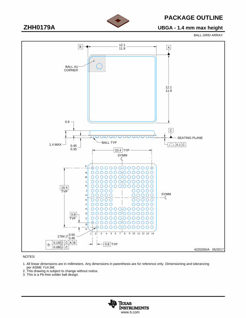
www.ti.com
PACKAGE OUTLINE
C
1.4 MAX 0.450.35
10.4TYP
10.4 TYP
0.8TYP
0.8 TYP
179X 0.550.45
0.9
B 12.111.9 A
12.111.9
4220265/A 05/2017
UBGA - 1.4 mm max heightZHH0179ABALL GRID ARRAY
NOTES: 1. All linear dimensions are in millimeters. Any dimensions in parenthesis are for reference only. Dimensioning and tolerancing per ASME Y14.5M.2. This drawing is subject to change without notice.3. This is a Pb-free solder ball design.
BALL A1CORNER
SEATING PLANEBALL TYP
0.1 C
A
1 2 3
0.15 C A B0.08 C
4 5 6 7 8 9 10 11 12 13
SYMM
SYMM
B
C
D
E
F
G
H
J
K
L
M
N
P
14
SCALE 1.200

www.ti.com
EXAMPLE BOARD LAYOUT
0.05 MIN0.05 MAX
179X ( 0.4)
(0.8) TYP
(0.8) TYP
( 0.4)SOLDER MASKOPENING
( 0.4)METAL
4220265/A 05/2017
UBGA - 1.4 mm max heightZHH0179ABALL GRID ARRAY
NOTES: (continued) 4. Final dimensions may vary due to manufacturing tolerance considerations and also routing constraints. See Texas Instruments Literature No. SSZA002 (www.ti.com/lit/ssza002).
SOLDER MASK DETAILSNOT TO SCALE
SYMM
SYMM
C
1 2 3 4 5 6 7 8 9 10 11 12 13
A
B
D
E
F
G
H
J
K
L
M
N
LAND PATTERN EXAMPLEEXPOSED METAL SHOWN
SCALE: 8X
14
P
NON-SOLDER MASKDEFINED
(PREFERRED)
EXPOSEDMETALSOLDER MASK
OPENING
SOLDER MASKDEFINED
METAL UNDERSOLDER MASK
EXPOSEDMETAL

www.ti.com
EXAMPLE STENCIL DESIGN
179X 0.4
(0.8) TYP
(0.8) TYP
4220265/A 05/2017
UBGA - 1.4 mm max heightZHH0179ABALL GRID ARRAY
NOTES: (continued) 5. Laser cutting apertures with trapezoidal walls and rounded corners may offer better paste release.
SYMM
SYMM
1 2 3 4 5 6 7 8 9 10 11 12 13
C
A
B
D
E
F
G
H
J
K
L
M
N
SOLDER PASTE EXAMPLEBASED ON 0.15 mm THICK STENCIL
SCALE: 10X
14
P


IMPORTANT NOTICE
Texas Instruments Incorporated (TI) reserves the right to make corrections, enhancements, improvements and other changes to itssemiconductor products and services per JESD46, latest issue, and to discontinue any product or service per JESD48, latest issue. Buyersshould obtain the latest relevant information before placing orders and should verify that such information is current and complete.TI’s published terms of sale for semiconductor products (http://www.ti.com/sc/docs/stdterms.htm) apply to the sale of packaged integratedcircuit products that TI has qualified and released to market. Additional terms may apply to the use or sale of other types of TI products andservices.Reproduction of significant portions of TI information in TI data sheets is permissible only if reproduction is without alteration and isaccompanied by all associated warranties, conditions, limitations, and notices. TI is not responsible or liable for such reproduceddocumentation. Information of third parties may be subject to additional restrictions. Resale of TI products or services with statementsdifferent from or beyond the parameters stated by TI for that product or service voids all express and any implied warranties for theassociated TI product or service and is an unfair and deceptive business practice. TI is not responsible or liable for any such statements.Buyers and others who are developing systems that incorporate TI products (collectively, “Designers”) understand and agree that Designersremain responsible for using their independent analysis, evaluation and judgment in designing their applications and that Designers havefull and exclusive responsibility to assure the safety of Designers' applications and compliance of their applications (and of all TI productsused in or for Designers’ applications) with all applicable regulations, laws and other applicable requirements. Designer represents that, withrespect to their applications, Designer has all the necessary expertise to create and implement safeguards that (1) anticipate dangerousconsequences of failures, (2) monitor failures and their consequences, and (3) lessen the likelihood of failures that might cause harm andtake appropriate actions. Designer agrees that prior to using or distributing any applications that include TI products, Designer willthoroughly test such applications and the functionality of such TI products as used in such applications.TI’s provision of technical, application or other design advice, quality characterization, reliability data or other services or information,including, but not limited to, reference designs and materials relating to evaluation modules, (collectively, “TI Resources”) are intended toassist designers who are developing applications that incorporate TI products; by downloading, accessing or using TI Resources in anyway, Designer (individually or, if Designer is acting on behalf of a company, Designer’s company) agrees to use any particular TI Resourcesolely for this purpose and subject to the terms of this Notice.TI’s provision of TI Resources does not expand or otherwise alter TI’s applicable published warranties or warranty disclaimers for TIproducts, and no additional obligations or liabilities arise from TI providing such TI Resources. TI reserves the right to make corrections,enhancements, improvements and other changes to its TI Resources. TI has not conducted any testing other than that specificallydescribed in the published documentation for a particular TI Resource.Designer is authorized to use, copy and modify any individual TI Resource only in connection with the development of applications thatinclude the TI product(s) identified in such TI Resource. NO OTHER LICENSE, EXPRESS OR IMPLIED, BY ESTOPPEL OR OTHERWISETO ANY OTHER TI INTELLECTUAL PROPERTY RIGHT, AND NO LICENSE TO ANY TECHNOLOGY OR INTELLECTUAL PROPERTYRIGHT OF TI OR ANY THIRD PARTY IS GRANTED HEREIN, including but not limited to any patent right, copyright, mask work right, orother intellectual property right relating to any combination, machine, or process in which TI products or services are used. Informationregarding or referencing third-party products or services does not constitute a license to use such products or services, or a warranty orendorsement thereof. Use of TI Resources may require a license from a third party under the patents or other intellectual property of thethird party, or a license from TI under the patents or other intellectual property of TI.TI RESOURCES ARE PROVIDED “AS IS” AND WITH ALL FAULTS. TI DISCLAIMS ALL OTHER WARRANTIES ORREPRESENTATIONS, EXPRESS OR IMPLIED, REGARDING RESOURCES OR USE THEREOF, INCLUDING BUT NOT LIMITED TOACCURACY OR COMPLETENESS, TITLE, ANY EPIDEMIC FAILURE WARRANTY AND ANY IMPLIED WARRANTIES OFMERCHANTABILITY, FITNESS FOR A PARTICULAR PURPOSE, AND NON-INFRINGEMENT OF ANY THIRD PARTY INTELLECTUALPROPERTY RIGHTS. TI SHALL NOT BE LIABLE FOR AND SHALL NOT DEFEND OR INDEMNIFY DESIGNER AGAINST ANY CLAIM,INCLUDING BUT NOT LIMITED TO ANY INFRINGEMENT CLAIM THAT RELATES TO OR IS BASED ON ANY COMBINATION OFPRODUCTS EVEN IF DESCRIBED IN TI RESOURCES OR OTHERWISE. IN NO EVENT SHALL TI BE LIABLE FOR ANY ACTUAL,DIRECT, SPECIAL, COLLATERAL, INDIRECT, PUNITIVE, INCIDENTAL, CONSEQUENTIAL OR EXEMPLARY DAMAGES INCONNECTION WITH OR ARISING OUT OF TI RESOURCES OR USE THEREOF, AND REGARDLESS OF WHETHER TI HAS BEENADVISED OF THE POSSIBILITY OF SUCH DAMAGES.Unless TI has explicitly designated an individual product as meeting the requirements of a particular industry standard (e.g., ISO/TS 16949and ISO 26262), TI is not responsible for any failure to meet such industry standard requirements.Where TI specifically promotes products as facilitating functional safety or as compliant with industry functional safety standards, suchproducts are intended to help enable customers to design and create their own applications that meet applicable functional safety standardsand requirements. Using products in an application does not by itself establish any safety features in the application. Designers mustensure compliance with safety-related requirements and standards applicable to their applications. Designer may not use any TI products inlife-critical medical equipment unless authorized officers of the parties have executed a special contract specifically governing such use.Life-critical medical equipment is medical equipment where failure of such equipment would cause serious bodily injury or death (e.g., lifesupport, pacemakers, defibrillators, heart pumps, neurostimulators, and implantables). Such equipment includes, without limitation, allmedical devices identified by the U.S. Food and Drug Administration as Class III devices and equivalent classifications outside the U.S.TI may expressly designate certain products as completing a particular qualification (e.g., Q100, Military Grade, or Enhanced Product).Designers agree that it has the necessary expertise to select the product with the appropriate qualification designation for their applicationsand that proper product selection is at Designers’ own risk. Designers are solely responsible for compliance with all legal and regulatoryrequirements in connection with such selection.Designer will fully indemnify TI and its representatives against any damages, costs, losses, and/or liabilities arising out of Designer’s non-compliance with the terms and provisions of this Notice.
Mailing Address: Texas Instruments, Post Office Box 655303, Dallas, Texas 75265Copyright © 2018, Texas Instruments Incorporated

Mouser Electronics
Authorized Distributor
Click to View Pricing, Inventory, Delivery & Lifecycle Information: Texas Instruments:
TMS320F2812GHHA TMS320F2812GHHAR TMS320F2812GHHQ TMS320F2812GHHS TMS320F2812PGFA
TMS320F2812PGFQ TMS320F2812PGFS TMS320F2812ZHHA TMS320F2812ZHHQ TMS320F2812ZHHS
TMS320F2812ZHHAR TYCOF2812PGFA SMAF2812PGFA TMS320F2812PGFAG4 DFDF2812ZHHAR
Related Documents