Application Report SPRA605 - February 2000 1 TMS320F240 DSP Solution for Obtaining Resolver Angular Position and Speed Martin Staebler DSP Field Application ABSTRACT This application report presents a TMS320F240 DSP solution for obtaining the angular position and speed of a resolver. A resolver is an absolute mechanical position sensor used, for example, in servo applications. It is basically a rotating transformer. The sinusoidal input reference is amplitude modulated with the sine and cosine of the mechanical angle, respectively. These two output signals have to be decoded to obtain the angular position. For decoding the resolver output signals, a basic method is introduced. It utilizes undersampling and an inverse tangent function. To achieve a higher angular resolution an improved method, which adds oversampling techniques is used. Due to an integral invariant filter, which is a combination of an IIR and FIR filter, the digitized angular position does not suffer any velocity lag. Thanks to its peripherals, the Texas Instruments TI TMS320F240 DSP can be ideally used for decoding the two resolver output signals as well as for generating the input reference frequency. The hardware interfacing of the resolver to the TMS320F240 is shown and the software realization of the improved method on the TMS320F240 is documented. All software routines are C-compatible. The angular resolution achievable with the TMS320F240 is up to 14 bits, at a CPU loading of 13%. Thus, the TMS320F240 will eliminate the cost for the external resolver-to-digital conversion IC, since the algorithm runs in addition to the motor control task. Contents 1 Introduction 2 . . . . . . . . . . . . . . . . . . . . . . . . . . . . . . . . . . . . . . . . . . . . . . . . . . . . . . . . . . . . . . . . . . . . . . . . . 2 The Resolver – An Absolute Angle Transducer 3 . . . . . . . . . . . . . . . . . . . . . . . . . . . . . . . . . . . . . . . . . 3 Obtaining Angular Position and Speed of the Resolver 5 . . . . . . . . . . . . . . . . . . . . . . . . . . . . . . . . . 3.1 Resolver-to-Digital (R/D) Conversion – using Undersampling 5 . . . . . . . . . . . . . . . . . . . . . . . . . . . 3.2 R/D Conversion – Improved Method Using Oversampling 6 . . . . . . . . . . . . . . . . . . . . . . . . . . . . . . 3.2.1 Overview 6 . . . . . . . . . . . . . . . . . . . . . . . . . . . . . . . . . . . . . . . . . . . . . . . . . . . . . . . . . . . . . . . . . 3.2.2 Dither – Adding Random White Noise 6 . . . . . . . . . . . . . . . . . . . . . . . . . . . . . . . . . . . . . . . . 3.2.3 FIR Decimation Bandpass-Filter 7 . . . . . . . . . . . . . . . . . . . . . . . . . . . . . . . . . . . . . . . . . . . . . 3.2.4 Arc Tangent Function 7 . . . . . . . . . . . . . . . . . . . . . . . . . . . . . . . . . . . . . . . . . . . . . . . . . . . . . . . 3.2.5 Closed-Loop Angular Position and Speed Interpolator 8 . . . . . . . . . . . . . . . . . . . . . . . . . . TI is a trademark of Texas Instruments Incorporated

Welcome message from author
This document is posted to help you gain knowledge. Please leave a comment to let me know what you think about it! Share it to your friends and learn new things together.
Transcript
Application ReportSPRA605 - February 2000
1
TMS320F240 DSP Solution for Obtaining ResolverAngular Position and Speed
Martin Staebler DSP Field Application
ABSTRACT
This application report presents a TMS320F240 DSP solution for obtaining the angularposition and speed of a resolver.
A resolver is an absolute mechanical position sensor used, for example, in servoapplications. It is basically a rotating transformer. The sinusoidal input reference is amplitudemodulated with the sine and cosine of the mechanical angle, respectively. These two outputsignals have to be decoded to obtain the angular position.
For decoding the resolver output signals, a basic method is introduced. It utilizesundersampling and an inverse tangent function. To achieve a higher angular resolution animproved method, which adds oversampling techniques is used. Due to an integral invariantfilter, which is a combination of an IIR and FIR filter, the digitized angular position does notsuffer any velocity lag.
Thanks to its peripherals, the Texas Instruments TI TMS320F240 DSP can be ideally usedfor decoding the two resolver output signals as well as for generating the input referencefrequency. The hardware interfacing of the resolver to the TMS320F240 is shown and thesoftware realization of the improved method on the TMS320F240 is documented. Allsoftware routines are C-compatible. The angular resolution achievable with theTMS320F240 is up to 14 bits, at a CPU loading of 13%.
Thus, the TMS320F240 will eliminate the cost for the external resolver-to-digital conversionIC, since the algorithm runs in addition to the motor control task.
Contents
1 Introduction 2. . . . . . . . . . . . . . . . . . . . . . . . . . . . . . . . . . . . . . . . . . . . . . . . . . . . . . . . . . . . . . . . . . . . . . . . .
2 The Resolver – An Absolute Angle Transducer 3. . . . . . . . . . . . . . . . . . . . . . . . . . . . . . . . . . . . . . . . .
3 Obtaining Angular Position and Speed of the Resolver 5. . . . . . . . . . . . . . . . . . . . . . . . . . . . . . . . . 3.1 Resolver-to-Digital (R/D) Conversion – using Undersampling 5. . . . . . . . . . . . . . . . . . . . . . . . . . . 3.2 R/D Conversion – Improved Method Using Oversampling 6. . . . . . . . . . . . . . . . . . . . . . . . . . . . . .
3.2.1 Overview 6. . . . . . . . . . . . . . . . . . . . . . . . . . . . . . . . . . . . . . . . . . . . . . . . . . . . . . . . . . . . . . . . . 3.2.2 Dither – Adding Random White Noise 6. . . . . . . . . . . . . . . . . . . . . . . . . . . . . . . . . . . . . . . . 3.2.3 FIR Decimation Bandpass-Filter 7. . . . . . . . . . . . . . . . . . . . . . . . . . . . . . . . . . . . . . . . . . . . . 3.2.4 Arc Tangent Function 7. . . . . . . . . . . . . . . . . . . . . . . . . . . . . . . . . . . . . . . . . . . . . . . . . . . . . . . 3.2.5 Closed-Loop Angular Position and Speed Interpolator 8. . . . . . . . . . . . . . . . . . . . . . . . . .
TI is a trademark of Texas Instruments Incorporated
SPRA605
2 TMS320F240 DSP Solution for Obtaining Resolver Angular Position and Speed
4 TMS320F240 DSP Implementation 9. . . . . . . . . . . . . . . . . . . . . . . . . . . . . . . . . . . . . . . . . . . . . . . . . . . . 4.1 Overview 9. . . . . . . . . . . . . . . . . . . . . . . . . . . . . . . . . . . . . . . . . . . . . . . . . . . . . . . . . . . . . . . . . . . . . . . . 4.2 TMS320F240 Hardware Interface 10. . . . . . . . . . . . . . . . . . . . . . . . . . . . . . . . . . . . . . . . . . . . . . . . . . 4.3 TMS320F240 Software Implementation 11. . . . . . . . . . . . . . . . . . . . . . . . . . . . . . . . . . . . . . . . . . . .
4.3.1 Program Structure 11. . . . . . . . . . . . . . . . . . . . . . . . . . . . . . . . . . . . . . . . . . . . . . . . . . . . . . . . 4.3.2 TMS320F240 DSP Initialization 12. . . . . . . . . . . . . . . . . . . . . . . . . . . . . . . . . . . . . . . . . . . . . 4.3.3 Interrupt Service Routine 13. . . . . . . . . . . . . . . . . . . . . . . . . . . . . . . . . . . . . . . . . . . . . . . . . . . 4.3.4 R/D Conversion using Oversampling 14. . . . . . . . . . . . . . . . . . . . . . . . . . . . . . . . . . . . . . . .
4.4 Changing Parameters 18. . . . . . . . . . . . . . . . . . . . . . . . . . . . . . . . . . . . . . . . . . . . . . . . . . . . . . . . . . . . 4.4.1 Reference Frequency 18. . . . . . . . . . . . . . . . . . . . . . . . . . . . . . . . . . . . . . . . . . . . . . . . . . . . . . 4.4.2 Angular Resolution and Bandwidth 18. . . . . . . . . . . . . . . . . . . . . . . . . . . . . . . . . . . . . . . . . .
5 Results 18. . . . . . . . . . . . . . . . . . . . . . . . . . . . . . . . . . . . . . . . . . . . . . . . . . . . . . . . . . . . . . . . . . . . . . . . . . . . 5.1 Processor Utilization 18. . . . . . . . . . . . . . . . . . . . . . . . . . . . . . . . . . . . . . . . . . . . . . . . . . . . . . . . . . . . . 5.2 Angular Accuracy and Transient Response 19. . . . . . . . . . . . . . . . . . . . . . . . . . . . . . . . . . . . . . . . .
6 Conclusion 21. . . . . . . . . . . . . . . . . . . . . . . . . . . . . . . . . . . . . . . . . . . . . . . . . . . . . . . . . . . . . . . . . . . . . . . . . 7 References 22. . . . . . . . . . . . . . . . . . . . . . . . . . . . . . . . . . . . . . . . . . . . . . . . . . . . . . . . . . . . . . . . . . . . . . . . .
List of Figures
Figure 1. Resolver, Simplified Functional Diagram and Corresponding Signals 4. . . . . . . . . . . . . . . . . . . . Figure 2. Amplitude Spectrum of the Resolver Signals u1, u2 4. . . . . . . . . . . . . . . . . . . . . . . . . . . . . . . . . . . Figure 3. Resolver-to-Digital Conversion Utilizing Undersampling and Inverse Tangent 5. . . . . . . . . . . . . Figure 4. Block Diagram of the Improved Resolver-to-Digital Converter 6. . . . . . . . . . . . . . . . . . . . . . . . . . Figure 5. FIR Decimation Bandpass Filter Magnitude Response 7. . . . . . . . . . . . . . . . . . . . . . . . . . . . . . . . Figure 6. Angular Error as Function of the Rotational Speed After the FIR Filter 8. . . . . . . . . . . . . . . . . . . Figure 7. Closed-Loop Position and Speed Interpolator 8. . . . . . . . . . . . . . . . . . . . . . . . . . . . . . . . . . . . . . . . Figure 8. Functional Block Diagram of the TMS320F240 R/D Converter Realization 9. . . . . . . . . . . . . . . Figure 9. Signal conditioning for resolver to TMS320F240 interface 10. . . . . . . . . . . . . . . . . . . . . . . . . . . . Figure 10. Signal Conditioning for Single-Ended Resolver Signals 11. . . . . . . . . . . . . . . . . . . . . . . . . . . . . . Figure 11. Flowchart of timer3_int 13. . . . . . . . . . . . . . . . . . . . . . . . . . . . . . . . . . . . . . . . . . . . . . . . . . . . . . . . . . Figure 12. Magnitude Response of the 17-Tap FIR Filter 16. . . . . . . . . . . . . . . . . . . . . . . . . . . . . . . . . . . . . . Figure 13. Closed-Loop Angle and Speed Interpolator 17. . . . . . . . . . . . . . . . . . . . . . . . . . . . . . . . . . . . . . . . Figure 14. Normalized Step Response of the Interpolated Angle 17. . . . . . . . . . . . . . . . . . . . . . . . . . . . . . . Figure 15. Measured Normalized Step Response for a 1º Angular Step (1º ~ 180). 19. . . . . . . . . . . . . . . Figure 16. Resolver angular position and angular speed 20. . . . . . . . . . . . . . . . . . . . . . . . . . . . . . . . . . . . . . Figure 17. Angular Position Error for a Speed Reversal From –180 rpm to +180 rpm 20. . . . . . . . . . . . . Figure 18. As Figure 17, but y-Axis Zoomed 21. . . . . . . . . . . . . . . . . . . . . . . . . . . . . . . . . . . . . . . . . . . . . . . . .
List of Tables
Table 1. Source Modules and Functional Description 12. . . . . . . . . . . . . . . . . . . . . . . . . . . . . . . . . . . . . . . . . Table 2. Angular Resolution and Bandwidth as Function of KI and KP 18. . . . . . . . . . . . . . . . . . . . . . . . . . Table 3. TMS320F240 CPU Loading 18. . . . . . . . . . . . . . . . . . . . . . . . . . . . . . . . . . . . . . . . . . . . . . . . . . . . . . . Table 4. Angular Accuracy and Settling Time Versus Bandwidth 19. . . . . . . . . . . . . . . . . . . . . . . . . . . . . . . .
1 IntroductionDigital signal processors are going to become more common in digital motor controlapplications. They permit sophisticated real-time control applications to be implemented, whichimprove dynamic response, precision and efficiency. In addition, they enable sensorless control,which reduces total system operating by eliminating mechanical sensors.

SPRA605
3 TMS320F240 DSP Solution for Obtaining Resolver Angular Position and Speed
TMS320F240 has been successfully used in sensorless applications. Mechanical sensors,which provide information on speed or position of the drive, can be eliminated and replaced byhigh-sophisticated position and speed estimation algorithms. Typical estimation algorithmsinclude Extended-Kalman-Filters, INFORM, and Sliding Mode Observers. A further costreduction can be achieved by the elimination of phase current sensors by a new algorithm thatestimates the actual value of the three phase currents using only the DC-link current with ashunt resistor.
However, there are still applications where sensorless control cannot achieve the requiredaccuracy and reliability. This is especially true with respect to the angular position. Examplesinclude servo applications, like robotics and numerically controlled machine tools. Mechanicalsensors used there are usually incremental encoders and resolvers.
Incremental TTL-encoders provide a pulse train, where each pulse is equivalent to anincremental step. Incremental encoders with sinusoidal output voltage allow interpolationbetween two incremental steps and achieve a higher accuracy. Incremental encoders arerelative position sensors. In contrast, resolvers are absolute angle transducers. They providetwo output signals that always allow the detection of the absolute angular position. This and thefact that they suppress common mode noise, makes them especially useful in a noisyenvironment.
Since decoding the output signals of a resolver is not straightforward, application specific ICs,called resolver-to-digital converters, have been used to track the resolver’s angular position.
This application report presents a TMS320F240 DSP solution for resolver-to-digital conversion,which runs in addition to the motor control task. This will eliminate the cost for the external ICand provide improved performance and flexibility, since parameters can be easily modified bysoftware.
Section 2 gives an introduction to the functionality of a resolver. Section 3 introduces thealgorithm to obtain angular position and speed with a resolver. Section 4 then describes thehardware and software implementation on the TMS320F240 DSP controller. Finally section 5shows the results achieved with this TMS320F240 DSP solution.
2 The Resolver – An Absolute Angle Transducer
Resolvers are absolute angle transducers and are mounted on the motor shaft to get the motor’sabsolute angular position. The accuracy is typically in the range of 5 arcmin. Resolvers are oftenused for angle sensing in noisy environment, due to their rugged construction and their ability toreject common mode noise.
Resolvers are basically rotating transformers. A simplified functional diagram of a resolver andits corresponding signals over one mechanical revolution is depicted in Figure 1.
SPRA605
4 TMS320F240 DSP Solution for Obtaining Resolver Angular Position and Speed
U2
U0U1
ε
0 45 90 135 180 225 270 315 360
U0
U1
U2
ε
Figure 1. Resolver, Simplified Functional Diagram and Corresponding Signals
It basically consists of a rotor coil, with N windings and two orthogonal stator coils with usually Nor N/2 windings. An alternating voltage, the reference signal, is coupled into the rotor windingand provides primary excitation. The reference signal is typically a fixed frequency in the rangeof 2kHz to 10kHz, with:
u0(t) � u^ 0 · sin�reft
The two orthogonal stator coils are wound, so that when the rotor shaft turns, the amplitude ofthe output signals is modulated with the sine and cosine of the shaft angle ε, relative to somezero, according to:
u1 (�, t) � u^ 0 · k · sin� · sin�reft
u2 (�, t) � u^ 0 · k · cos� · sin�reft
k is the transformation ratio of the resolver. Hence the shape of the resolver output signal u1 andu2 is equal to the sine and the cosine of the mechanical angle, respectively. Figure 2 shows theamplitude spectrum of the resolver output signals u1, u2, for a sinusoidal excitation signal u0.
freqfreffref–fB fref+fB
u1,2(f)
Figure 2. Amplitude Spectrum of the Resolver Signals u 1, u2
As with amplitude-modulated signals, the spectrum is symmetrical to the reference frequency.The bandwidth fB depends on the maximum angular speed according to:
fB �
12�
· d�dt MAX
SPRA605
5 TMS320F240 DSP Solution for Obtaining Resolver Angular Position and Speed
3 Obtaining Angular Position and Speed of the ResolverThe method for obtaining and digitizing the angular position of a resolver is also known asresolver-to-digital conversion (R/D conversion). One basic method, utilizing digital demodulation,is introduced in this section. It can be ideally implemented on the TMS320F240 DSP.
3.1 Resolver-to-Digital (R/D) Conversion – using Undersampling
The basic method is depicted in Figure 3. The sine and cosine modulated output signals u1 andu2 must be sampled at the same frequency as the reference frequency. This, so calledundersampling , demodulates both analog signals, so that the digitized samples u1(n) and u2(n)are sinε and cosε of the angle ε, respectively. This method can be ideally implemented on theTMS320F240. It incorporates dual ADCs, which can be synchronized to the referencefrequency, generated by the on-chip PWM-unit.
ADC
ADC
n n+1
����������
������
������������������ �� ������������� �������� �� �� �� �� ���
u1
u2
sin ε
cos ε
angle εD
N bit
N bit
N + bit
Figure 3. Resolver-to-Digital Conversion Utilizing Undersampling and Inverse Tangent
The angular position can now be determined by a four quadrant inverse tangent function of thequotient of the demodulated sine and cosine samples. The inverse tangent function isambiguous. Thus, the sign of the sampled signals has to be taken into account, in order todetermine the absolute angular position according to:
arctan�u1(n)
u2(n)�, if u2(n) � 0
� � arctan�u2(n)
u1(n)�, if u2(n) � 0
���� �
To be accurate, both signals, u1 and u2, have to be sampled simultaneously, at, or close to theirmaximum positive value, synchronized to the reference frequency according to:
������� �� ����������� �� � �� �� �� ����������
To avoid aliasing, the Nyquist criteria must be met. It requires the sample rate fS to be at leasttwice the bandwidth fB of the interesting signal. To meet that, an analog anti-alias filter has toremove any frequency components outside the band-of-interest fref ± fB. Referring to Figure 2, itis obvious that any DC offset has to be removed prior to sampling. Otherwise, it would be addedto the demodulated sine and cosine signals and decrease accuracy.
For an N-bit ADC, the angular accuracy achievable is N+1-bit. With the dual 10-bit ADCsintegrated on the TMS320F240, the angular accuracy achievable is 10 arc minutes. A higherresolution and better noise rejection are achievable by oversampling and averaging techniques,which are discussed in the following section.
SPRA605
6 TMS320F240 DSP Solution for Obtaining Resolver Angular Position and Speed
3.2 R/D Conversion – Improved Method Using Oversampling
3.2.1 Overview
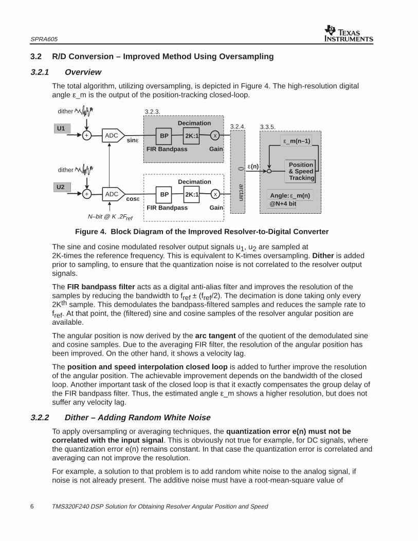
The total algorithm, utilizing oversampling, is depicted in Figure 4. The high-resolution digitalangle ε_m is the output of the position-tracking closed-loop.
FIR Bandpass
BP
Decimation
2K:1U1
cos ε
Position& Speed Tracking
Angle: ε_m(n)
ε(n)
ε_m(n–1)Gain
@N+4 bit
ADC+ x
arctan()
dither
FIR Bandpass
BP
Decimation
2K:1U2
Gain
ADC+ x
dither
sin ε
3.2.3.
3.2.4. 3.3.5.
N–bit @ K .2Fref
Figure 4. Block Diagram of the Improved Resolver-to-Digital Converter
The sine and cosine modulated resolver output signals u1, u2 are sampled at 2K-times the reference frequency. This is equivalent to K-times oversampling. Dither is addedprior to sampling, to ensure that the quantization noise is not correlated to the resolver outputsignals.
The FIR bandpass filter acts as a digital anti-alias filter and improves the resolution of thesamples by reducing the bandwidth to fref ± (fref/2). The decimation is done taking only every2Kth sample. This demodulates the bandpass-filtered samples and reduces the sample rate tofref. At that point, the (filtered) sine and cosine samples of the resolver angular position areavailable.
The angular position is now derived by the arc tangent of the quotient of the demodulated sineand cosine samples. Due to the averaging FIR filter, the resolution of the angular position hasbeen improved. On the other hand, it shows a velocity lag.
The position and speed interpolation closed loop is added to further improve the resolutionof the angular position. The achievable improvement depends on the bandwidth of the closedloop. Another important task of the closed loop is that it exactly compensates the group delay ofthe FIR bandpass filter. Thus, the estimated angle ε_m shows a higher resolution, but does notsuffer any velocity lag.
3.2.2 Dither – Adding Random White Noise
To apply oversampling or averaging techniques, the quantization error e(n) must not becorrelated with the input signal . This is obviously not true for example, for DC signals, wherethe quantization error e(n) remains constant. In that case the quantization error is correlated andaveraging can not improve the resolution.
For example, a solution to that problem is to add random white noise to the analog signal, ifnoise is not already present. The additive noise must have a root-mean-square value of
SPRA605
7 TMS320F240 DSP Solution for Obtaining Resolver Angular Position and Speed
rms(noise) � q�12� , q � 1LSB
This ensures that the quantization error is not correlated with the input signal. Note that thisdoes not increase the total quantization error.
3.2.3 FIR Decimation Bandpass-Filter
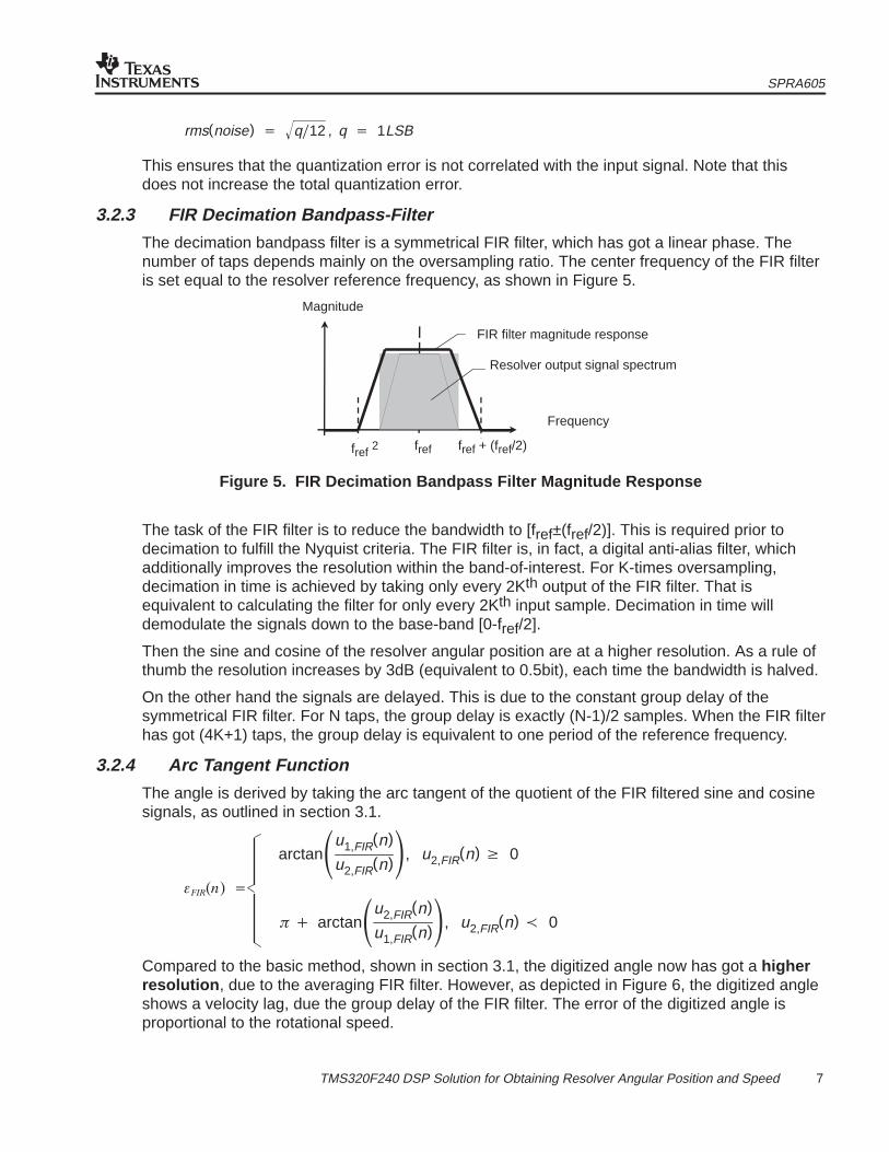
The decimation bandpass filter is a symmetrical FIR filter, which has got a linear phase. Thenumber of taps depends mainly on the oversampling ratio. The center frequency of the FIR filteris set equal to the resolver reference frequency, as shown in Figure 5.
Magnitude
FIR filter magnitude response
Resolver output signal spectrum
Frequency
fref + (fref/2)fref 2 fref
Figure 5. FIR Decimation Bandpass Filter Magnitude Response
The task of the FIR filter is to reduce the bandwidth to [fref±(fref/2)]. This is required prior todecimation to fulfill the Nyquist criteria. The FIR filter is, in fact, a digital anti-alias filter, whichadditionally improves the resolution within the band-of-interest. For K-times oversampling,decimation in time is achieved by taking only every 2Kth output of the FIR filter. That isequivalent to calculating the filter for only every 2Kth input sample. Decimation in time willdemodulate the signals down to the base-band [0-fref/2].
Then the sine and cosine of the resolver angular position are at a higher resolution. As a rule ofthumb the resolution increases by 3dB (equivalent to 0.5bit), each time the bandwidth is halved.
On the other hand the signals are delayed. This is due to the constant group delay of thesymmetrical FIR filter. For N taps, the group delay is exactly (N-1)/2 samples. When the FIR filterhas got (4K+1) taps, the group delay is equivalent to one period of the reference frequency.
3.2.4 Arc Tangent Function
The angle is derived by taking the arc tangent of the quotient of the FIR filtered sine and cosinesignals, as outlined in section 3.1.
arctan�u1,FIR(n)
u2,FIR(n)�, u2,FIR(n) � 0
� � arctan�u2,FIR(n)
u1,FIR(n)�, u2,FIR(n) � 0
�������� �
Compared to the basic method, shown in section 3.1, the digitized angle now has got a higherresolution , due to the averaging FIR filter. However, as depicted in Figure 6, the digitized angleshows a velocity lag, due the group delay of the FIR filter. The error of the digitized angle isproportional to the rotational speed.

SPRA605
8 TMS320F240 DSP Solution for Obtaining Resolver Angular Position and Speed
t_delay (FIR)
angular error
t_delay (FIR)
angular error
t
digital angle after FIR [ε_FIR]
resolver angle [ε]
angle [rad]
Figure 6. Angular Error as Function of the Rotational Speed After the FIR Filter
A closed-loop position and speed interpolator will be used to compensate for the angular errorand to further improve the angular resolution.
3.2.5 Closed-Loop Angular Position and Speed Interpolator
The closed-loop, shown in Figure 7, consists of a PI controller, a 1st order IIR filter and anintegrator. It is basically a lowpass filter. It is a type 2 closed-loop (two integrators) and hencedoes not have an integral error. The parameters of the closed-loop define bandwidth andcharacteristic and are discussed in the next section.
The task of the closed-loop is to:
• Improve the accuracy of the angular position ε_m. The accuracy depends on bandwidthselected.
• Compensate the delay of the FIR filter, so that ε_m suffers no velocity lag
• Derive the angular speed ω_m
The result will be a higher accuracy of the interpolated angular position ε_m. Additionally ε_mdoes not suffer a velocity lag.
This is achieved by the following. The output signal ε_m is delayed with the same time as theFIR filters group delay. Hence the delayed output signal ε_m(n–1) is also compared with thedelayed FIR filtered angle ε_FIR. The closed-loop forces both delayed angles to be identical. Forconstant speeds, the output ε_m of the closed-loop is then identical with the real resolver shaftangle.
PI controllerIIR
Σ
Integrator
–
+
Z–1
ε_m ω_m ε_FIR
Figure 7. Closed-Loop Position and Speed Interpolator

SPRA605
9 TMS320F240 DSP Solution for Obtaining Resolver Angular Position and Speed
4 TMS320F240 DSP Implementation
4.1 Overview
The TMS320F240 DSP controller incorporates two 10-bit A/D converters, which sample bothanalog inputs simultaneously. The A/D sampling point can be triggered by any timer event,hence synchronously to the on-chip PWM. One PWM channel (part of the event manager) isused to generate the sinusoidal reference frequency.
U2
U0U1
εC2xxDSP
16KW FLASH
EVENT MGR
WD
SCI
SPI
10–bit A/D10–bit A/D
28 bit I/O
PLL
H/W interfaceTMS320F240 Resolver
(20 MIPS)
Figure 8. Functional Block Diagram of the TMS320F240 R/D Converter Realization
Figure 8 shows the TMS320F240 single-chip DSP solution for the resolver-to-digital conversion.The DSP performs the following tasks:
• Generates the sinusoidal reference frequency [Event Manager]
• Sample both resolver output signals simultaneously [ADC]
• Synchronizes the sampling point to the sinusoidal frequency [ADC, Event Manager]
• Performs the improved R/D conversion algorithm outlined in section 3 [CPU]
SPRA605
10 TMS320F240 DSP Solution for Obtaining Resolver Angular Position and Speed
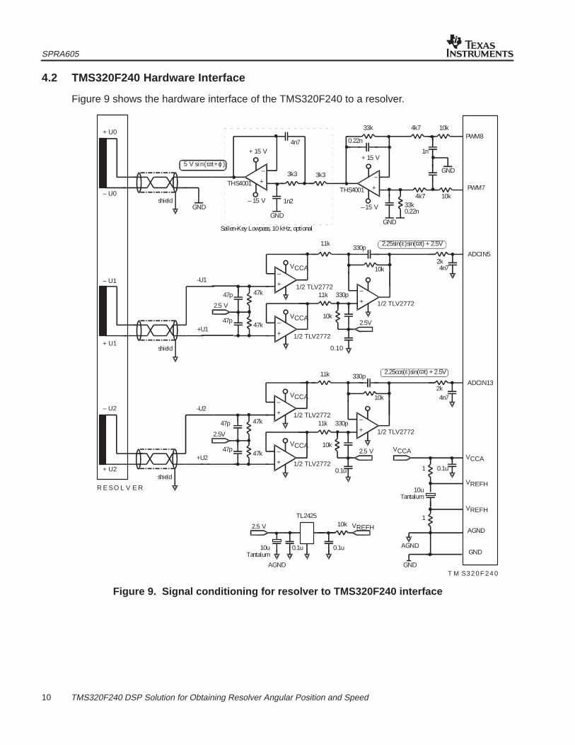
4.2 TMS320F240 Hardware Interface
Figure 9 shows the hardware interface of the TMS320F240 to a resolver.
+
–
+
–
+
–
2.5 V
2.5 V
AGND
ADCIN13
AGND
GND
GND
shield
2k4n7
0.1u1
1
0.1u
TL2425
11k
10k
0.1u
PWM7
T M S32 0F 24 0
R E SO L V E R
11k
10k
+
–
330p
330p
THS4001
10uTantalum
AGND
10uTantalum
0.1u
10k
2.5V
+U2
–U2
47k
47k
+
–
+
–
+
–
2.5V
ADCIN5
shield
2k4n7
11k
10k
11k
10k
330p
330p
2.5 V
+U1
–U1
47k
47k
47p
PWM8
GND
GND
+ 15 V
–15 V
10k
10k
4k7
4k7
33k
33k
1n
0.22n
0.22n
+
–
THS4001
GND
+ 15 V
– 15 V
Sallen–Key Lowpass, 10 kHz, optional
4n7
1n2
3k3 3k3
shield
+ U0
GND
47p
47p
47p
5 V sin(ωt+ϕ )
2.25cos(ε)sin(ωt) + 2.5V
2.25sin(ε)sin(ωt) + 2.5V
– U0
VCCA
1/2 TLV2772
1/2 TLV2772
1/2 TLV2772
0.10
VCCA
VCCA
VCCA
1/2 TLV2772
1/2 TLV2772
VCCAVCCA
VREFH
VREFH
VREFH
– U1
+ U1
– U2
+ U2
1/2 TLV2772
Figure 9. Signal conditioning for resolver to TMS320F240 interface

SPRA605
11 TMS320F240 DSP Solution for Obtaining Resolver Angular Position and Speed
Note that the values of the components are valid for a 5-kHz reference with a 10 VPPpeak-to-peak voltage and a resolver with a transformation ratio of 2:1. Thus, the maximumpeak-to-peak voltage of the two modulated resolver output signals is 5 VPP.
The circuit performs the following:
• Signal conditioning of the PWM output to drive the resolver with a sinusoidal referencefrequency u0.
The PWM channels PWM7 and PWM8 (differential signals) are used to generate thesinusoidal reference frequency. The first op amp THS4001 is used to filter out the PWMcarrier signal, to do the level shifting and amplification to get a sine wave at 10Vpp outputvoltage swing. The second op amp performs a Sallen-Key lowpass filter and further reducesharmonic distortion.
• Signal conditioning and level shifting of both resolver output signals, u1, u2 to drive theTMS320F240 A/D converters.
The differential output signals of the resolver are fed into non-inverting buffers TLV2772 andreferenced to the virtual ground. The following differential amplifier TLV2772 suppressescommon mode noise and performs the level shifting to meet the 5-V A/D input range. TheTL2772 are single supply, rail-to-rail output CMOS op amps. The RC network performs theanti-alias filter. The capacitor is chosen to drive the A/D module switch capacitor input, ratherthan the op amp. Therefore the capacitor should be as close as possible to the analog inputpins ADCIN5 and ADCIN13, respectively.
• The TL2425 provides the 2.5V virtual ground, to operate with single 5V supply only.
• TMS320F240 A/D input voltage range is 0 – 5 V.
Figure 10 shows a simpler solution for single-ended resolver output signals. It requires onlyone single op amp to do buffering and level shifting. However, due to AC coupling the gain ofeach channel is a function of the line impedance.
+–
2.5V A D CIN 5(A D CI N 13)
shield
1/2 T L V 2772 2k4n7
10k
10k
330p
100p
–U 1(U 2)
+ U 1(U 2)
V REFL
11k
10uT antalum
–U 1(U 2)
+U 1(U 2)
2 .25cos(ε) sin(ωt) + 2 .5V
V C CA
11k
2.25sin(ε)sin(ωt) + 2.5V
Figure 10. Signal Conditioning for Single-Ended Resolver Signals
4.3 TMS320F240 Software Implementation
4.3.1 Program Structure
The software is mainly written in ANSI C language to achieve a modular and readable softwarestructure. Only time critical functions, like the FIR filter, arc tangent, etc., are written in run-timeoptimized assembler, but provide a C-compatible interface. Hence these functions can also becalled from any C program.
SPRA605
12 TMS320F240 DSP Solution for Obtaining Resolver Angular Position and Speed
The software integrates all modules required to obtain the resolvers angular position and speed.It can be easily integrated, for example, in a standard field-oriented control. The source files anda short functional description are given in Table 1.
The software is basically structured into three main functional blocks. Each functional block isrealized as a C function, which might call other functions. The following three sections give adetailed description on these functions.
Table 1. Source Modules and Functional Description
Source Module C Callable Functions Functional Description
MAIN.C main() Main program
INIT.C Resolver_Init() ’F240 initialization
T3_INT.C timer3_int() Interrupt service routine
CONTROL.C control() R/D conversion, improved method
FIR_DEC8.ASM int FIRBandpass_17A_Dec8 (* int) 17-tap FIR decimation bandpass filter
CL.C Resolver_ClosedLoop() Closed-loop position and speed interpolator
ATAN_DIV.ASM int atan_div(int nom, int denom) Inverse tangent of the quotient sin/cos
4.3.2 TMS320F240 DSP Initialization
Function: void Resolver_Init(void)
This initialization routine is called from the main program and sets up the TMS320F240 and itsperipherals. The function does not pass any argument and does not return a value.
The TMS320F240 is setup with a CPU clock of 20MHz. The peripherals simple compare PWMunit, timer 3 and the ADC module and the timer 3 period interrupt are initialized.
• Timer 3 period interrupt is the main time base. The cycle time is 25us, hence the referencefrequency period is 200us, or 5 kHz.
• The simple compare units are used to generate the sinusoidal reference frequency andnoise, respectively. Timer2 is selected as the PWM time base. The timer2 period is set to �of the timer 3 period. This will give a PWM period of 6.25us. The reason for that is to reducethe ripple on the sine wave. This relaxes the requirements to the analog reconstruction filter.
• The resolver output signals, connected to ADCIN5, ADCIN13 are automatically sampled ona timer3 compare event. This guarantees that the sampling points are synchronized to thePWM unit, which generates the reference frequency. Triggering the conversion by a timer3compare event allows optimizing the phase at which the signal is sampled. The timer3compare value is initially set to 12.5us. This means that the signals are sampled 12.5usbefore the interrupt occurs. Any modification of the timer3 compare value shifts the samplingpoint and hence the phase at which the resolver signals are sampled within +/–22.5 degrees.However, the conversion time of 6us, prior to the timer3 period interrupt must still be met.
• All timers are synchronized and started synchronously.
Note: The corresponding header file INIT.H contains the values for the reference frequency andthe gain error of the two input channels at the analog inputs ADCIN5 and ADCIN13.

SPRA605
13 TMS320F240 DSP Solution for Obtaining Resolver Angular Position and Speed
4.3.3 Interrupt Service Routine
Interrupt: void interrupt timer3_int(void)
The timer 3 period interrupt is the only interrupt used. The interrupt cycle time is set to 25 µs.This is equivalent to 1/8 of the sinusoidal reference period of 200 µs or a 5kHz frequency. Theflowchart is depicted in Figure 11.
(timer3_int_count++)%32
read ADCIN5, ADCIN13
lookup sine valuegenerate random noise
write ADCIN5,13 to delay lineresolver_buffer [ ] [ ]
update PWM7/8(sine), 9(noise)
timer 3_int
RETI
call CONTROL
timer3_int_count%8=0?
yes
no
Figure 11. Flowchart of timer3_int
The variable timer3_int_count is used as a pointer and as a scheduler. It is incrementedeach timer 3 interrupt within the range 0–31. This modulo 32 operation is done by simplymasking the upper bits 5–15, respectively.
The tasks of the timer3_int interrupt routine are as follows:
• 4 x oversampling of the sine and cosine modulated resolver signals u1, connected toADCIN5 and u2, connected to ADCIN13
The ADC sample rate is synchronized with the sinusoidal reference frequency, which isgenerated by the TMS320F240 on-chip simple compare unit.
The ADC sampling point is triggered automatically by a timer3 compare event. This allowscompensating a phase shift of up to ±22.5� between the reference frequency u0 and themodulated resolver output signals u1 and u2. Thus, a modification of the timer3 comparevalue shifts the phase at which the signals are sampled. Note, that the timer3 compare eventmust occur no later than 6us before the timer3 period interrupt, to meet the ADC conversiontime of 6us.
The data of ADC1 FIFO (result of channel 5) and ADC2 FIFO (result of channel 13) isdivided by two to get a headroom of 6dB. An offset is added to convert to a 2s complement
SPRA605
14 TMS320F240 DSP Solution for Obtaining Resolver Angular Position and Speed
or Q15 fractional number. These Q15 numbers are stored into the delay lineresolver_buffer[][] . The variable timer3_int_count is used to point to the latest position inthe delay buffer according to:
resolver_buffer[0][timer3_int_count] = ADCFIFO1/2 + 32768
resolver_buffer[1][timer3_int_count] = ADCFIFO2/2 + 32768
The lower array resolver_buffer [0] [] always stores the latest 32 sine modulated samplesin Q15 notation with a 6dB headroom. The upper array resolver_buffer[1][] stores the latest32-cosine modulated samples, respectively.
• Resolver reference frequency generation via the simple compare PWM unit
The simple compare PWM unit, used to generated the sinusoidal reference frequency, isupdated in this interrupt — every 25 µs. This is equivalent to 8 updates during one period ofthe sine wave. Therefore a sine wave lookup table is used, which stores the corresponding 8PWM duty cycles. The elements are accessed according to:
PWM = sine_table [(timer3_int_count + sine_phase_lag) % 8]
The variable sine_phase_lag is used as an offset to the pointer timer_int_count and isinitialized, so that the output of the FIR filter is at a maximum.
To reduce harmonics the simple compare PWM period is 6.25 µs, which is � of timer3period. This reduces the amount of analog filtering and leads to a sine wave with lowerharmonic distortion.
• Random noise generation and update via the simple compare PWM9 unit
The noise generator is a random number generator, which calculates a new random numbereach timer 3 interrupt. The new random number is stored to the compare register of PWM9.
• Scheduling of the control() routine on every 8th interrupt.
The function control() is called on every 8th timer 3 interrupt. It performs theresolver-to-digital conversion algorithm and is explained in the next section.
4.3.4 R/D Conversion using Oversampling
This algorithm is realized using a level one function control(), written in C. This function callsthree level two functions, written in run-time optimized assembler. These areFIR_Bandpass_17A_Dec8 (* int), atan_div(int, int), Resolver_ClosedLoop().
Resolver position and speed are stored in the two global variables
• epsilon_m = high-resolution position without velocity lag
• omega_m = angular speed
Function: void interrupt control(void)
This function is called on every 8th timer 3 interrupt. With a 5 kHz reference frequency it is calledevery 200us. It performs the resolver-to-digital converter for obtaining the high-resolutionangular speed and position without any velocity lag. The listing of this function is shown below.

SPRA605
15 TMS320F240 DSP Solution for Obtaining Resolver Angular Position and Speed
void interrupt control(void){ int r_sin, r_cos;
asm(” eint”); /* enable interrupt */
/*––––––––––––––––––––––––––––––––*/ /* 17–tap FIR decimation bandpass */ /*––––––––––––––––––––––––––––––––*/ index = &resolver_buffer[0][timer3_int_count]; /* Ptr to latest */ /* element in delay line */ r_sin = FIRBandpass_17A_Dec8(index); r_cos = FIRBandpass_17A_Dec8(index+BUFFER_SIZE);
/*––––––––––––––––––––––––––––––*/ /* Gain compensation (optional) */ /*––––––––––––––––––––––––––––––*/ r_sin = (int) ((long)R_SIN_GAIN_Q15 * (long)r_sin >> 15); r_cos = (int) ((long)R_COS_GAIN_Q15 * (long)r_cos >> 15); /*–––––––––––––––––––––––––––––––––––––––––––––––––––––––––*/ /* Angle determination utilizing arc tangent function */ /*–––––––––––––––––––––––––––––––––––––––––––––––––––––––––*/ epsilon = atan_div(r_sin,r_cos); /* 200us delayed angle */
/*–––––––––––––––––––––––––––––––––––––––––––––––––––––––––*/ /* closed–loop angle and speed interpolation */ /*–––––––––––––––––––––––––––––––––––––––––––––––––––––––––*/ /* epsilon_m = actual position WITHOUT velocity lag */ /* omega_m = actual scaled speed */ /*–––––––––––––––––––––––––––––––––––––––––––––––––––––––––*/ Resolver_ClosedLoop();}
Note: The function control() could be used to include a PI current controller. If a faster currentcontroller cycle time is required, control() might be called on every 4th timer 3 interrupt and theresolver-to-digital algorithm is skipped every one, respectively.
Function: int FIR_Bandpass_17A_Dec8 (* int)
This function performs the bandpass filtering and decimation by 8, since it is called only every8th input sample. The variable sine_phase_lag is used as an offset to the pointertimer_int_count. It is initialized so, that the FIR filter takes always the window of 17 samples,which leads to the maximum output amplitude.
The argument passed to the filter is the pointer to the latest sample (start of the window) in thedelay line. The return value is the filtered signal.
The filter coefficients are designed with the Digital Filter Design Package [7]. It is a symmetricalFIR bandpass filter with 17 taps and a 5-kHz center frequency. The magnitude response isshown below.

SPRA605
16 TMS320F240 DSP Solution for Obtaining Resolver Angular Position and Speed
NOTE: Frequency scaled by 10.
Figure 12. Magnitude Response of the 17-Tap FIR Filter
This FIR filter reduces the S/N ratio within the signal band-of-interest 5kHz ± 2.5kHz by 9dB.This is equivalent to a bit gain of 1.5-bit. Another advantage of the FIR bandpass filter is thatnoise outside the band-of-interest 5kHz ± 2.5kHz is attenuated by more than 40dB. This isespecially required to remove any DC offset.
Function: int atan_div(int nom, int denom)
Arguments: nom, denom: Q15 (–1.0,..., 0.999)
Return: angle, Q15 (–1.0,.., 0.999), scaled by PI
Error: < 3 LSB
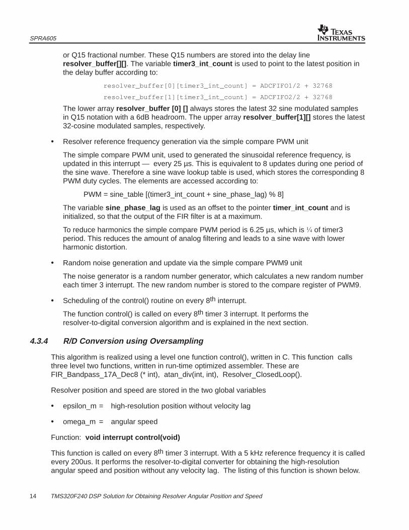
Function: void Resolver_ClosedLoop(void)
This function compensates the velocity lag of the angle, which is derived after the inversetangent function. It further improves the accuracy of the angular position and also calculates theangular speed. The achievable resolution depends on the bandwidth. The function requires thefollowing global input and output variables:
Global Input variables: epsilon (FIR filtered angle with velocity lag)
Global output variables: epsilon_m (high-resolution angle without velocity lag)
omega_m (high-resolution speed)
Figure 13 shows the block diagram of the closed loop. The settings of the parameters, whichdefine the bandwidth, are shown in the next section.
SPRA605
17 TMS320F240 DSP Solution for Obtaining Resolver Angular Position and Speed
z –1
z –1
z –1
z –1
+
x
x
x
++
x
x
+
x
e(n)
–kp
ki + kp u(n)
omega_m(n)epsilon_m(n)
+
a0 a1
b1 y(k)
epsilon(n)
– 1
PI controller IIR lowpass
Integrator
epsilon_m(n–1)
Figure 13. Closed-Loop Angle and Speed Interpolator
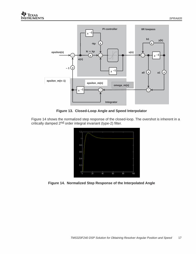
Figure 14 shows the normalized step response of the closed-loop. The overshot is inherent in acritically damped 2nd order integral invariant (type-2) filter.
Figure 14. Normalized Step Response of the Interpolated Angle
SPRA605
18 TMS320F240 DSP Solution for Obtaining Resolver Angular Position and Speed
4.4 Changing Parameters
4.4.1 Reference Frequency
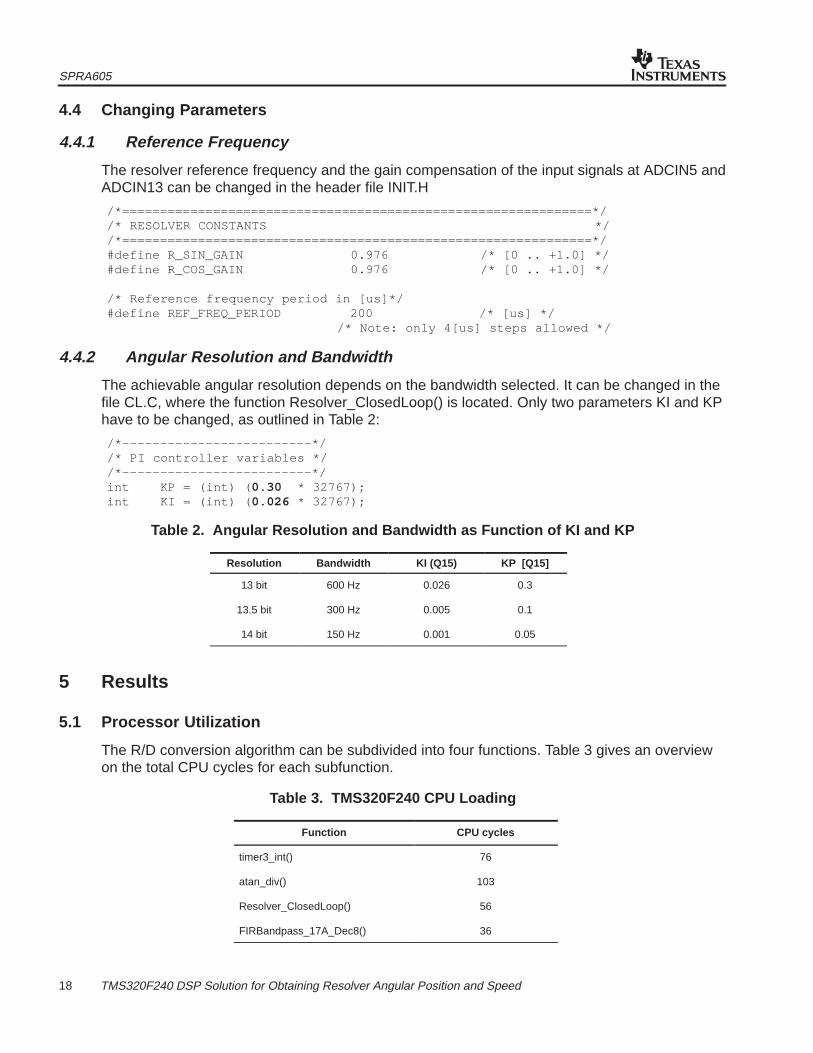
The resolver reference frequency and the gain compensation of the input signals at ADCIN5 andADCIN13 can be changed in the header file INIT.H
/*==============================================================*//* RESOLVER CONSTANTS *//*==============================================================*/#define R_SIN_GAIN 0.976 /* [0 .. +1.0] */#define R_COS_GAIN 0.976 /* [0 .. +1.0] */
/* Reference frequency period in [us]*/#define REF_FREQ_PERIOD 200 /* [us] */ /* Note: only 4[us] steps allowed */
4.4.2 Angular Resolution and Bandwidth
The achievable angular resolution depends on the bandwidth selected. It can be changed in thefile CL.C, where the function Resolver_ClosedLoop() is located. Only two parameters KI and KPhave to be changed, as outlined in Table 2:
/*–––––––––––––––––––––––––*//* PI controller variables *//*–––––––––––––––––––––––––*/int KP = (int) ( 0.30 * 32767);int KI = (int) ( 0.026 * 32767);
Table 2. Angular Resolution and Bandwidth as Function of KI and KP
Resolution Bandwidth KI (Q15) KP [Q15]
13 bit 600 Hz 0.026 0.3
13.5 bit 300 Hz 0.005 0.1
14 bit 150 Hz 0.001 0.05
5 Results
5.1 Processor Utilization
The R/D conversion algorithm can be subdivided into four functions. Table 3 gives an overviewon the total CPU cycles for each subfunction.
Table 3. TMS320F240 CPU Loading
Function CPU cycles
timer3_int() 76
atan_div() 103
Resolver_ClosedLoop() 56
FIRBandpass_17A_Dec8() 36
SPRA605
19 TMS320F240 DSP Solution for Obtaining Resolver Angular Position and Speed
All functions, except timer3_int(), are called every 200us, for a 5-kHz reference frequency. Theinterrupt routine is called 2-times the selected oversampling rate K. Thus, the total CPU loadingdepends mainly on the oversampling rate K.
The CPU loading, for the algorithm utilizing 4-times oversampling and a 5-kHz referencefrequency is approximately 13%. The CPU loading for two times oversampling will beapproximately 8%.
5.2 Angular Accuracy and Transient Response
The angular position resolution achievable with the TMS320F240 ranges from 12 to 14 bits,depending on the closed-loop bandwidth. The digital angular position does not show a velocitylag, thanks to the closed loop.
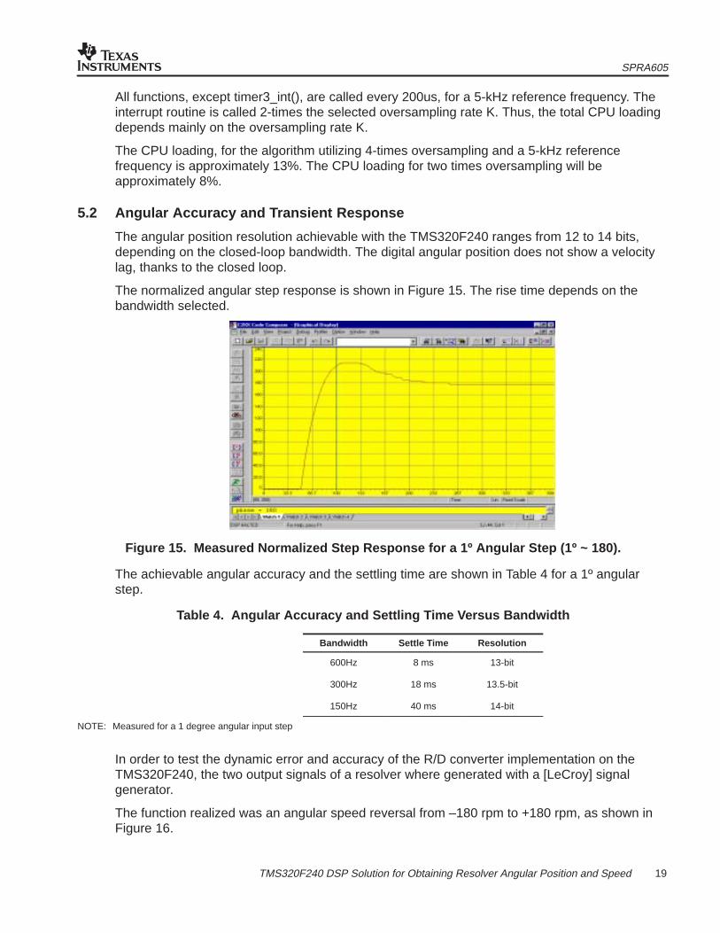
The normalized angular step response is shown in Figure 15. The rise time depends on thebandwidth selected.
Figure 15. Measured Normalized Step Response for a 1º Angular Step (1º ~ 180).
The achievable angular accuracy and the settling time are shown in Table 4 for a 1º angularstep.
Table 4. Angular Accuracy and Settling Time Versus Bandwidth
Bandwidth Settle Time Resolution
600Hz 8 ms 13-bit
300Hz 18 ms 13.5-bit
150Hz 40 ms 14-bit
NOTE: Measured for a 1 degree angular input step
In order to test the dynamic error and accuracy of the R/D converter implementation on theTMS320F240, the two output signals of a resolver where generated with a [LeCroy] signalgenerator.
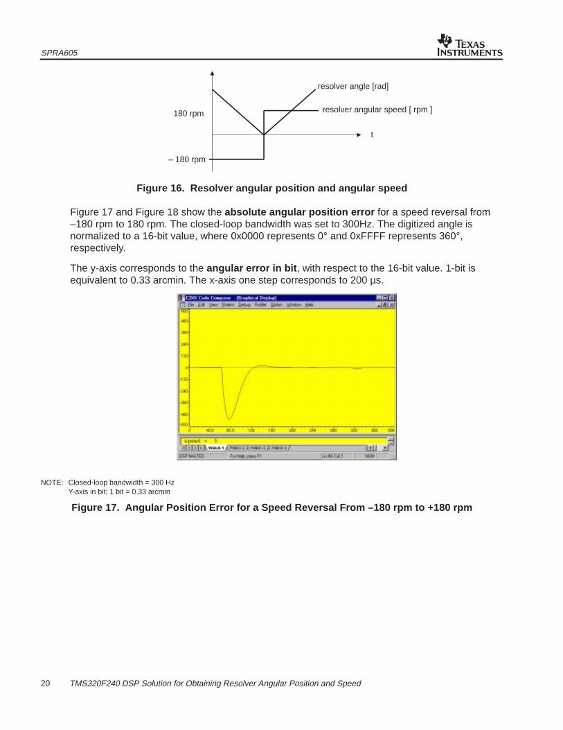
The function realized was an angular speed reversal from –180 rpm to +180 rpm, as shown inFigure 16.
SPRA605
20 TMS320F240 DSP Solution for Obtaining Resolver Angular Position and Speed
t
180 rpm
resolver angle [rad]
resolver angular speed [ rpm ]
– 180 rpm
Figure 16. Resolver angular position and angular speed
Figure 17 and Figure 18 show the absolute angular position error for a speed reversal from–180 rpm to 180 rpm. The closed-loop bandwidth was set to 300Hz. The digitized angle isnormalized to a 16-bit value, where 0x0000 represents 0° and 0xFFFF represents 360°,respectively.
The y-axis corresponds to the angular error in bit , with respect to the 16-bit value. 1-bit isequivalent to 0.33 arcmin. The x-axis one step corresponds to 200 µs.
NOTE: Closed-loop bandwidth = 300 HzY-axis in bit; 1 bit = 0.33 arcmin
Figure 17. Angular Position Error for a Speed Reversal From –180 rpm to +180 rpm

SPRA605
21 TMS320F240 DSP Solution for Obtaining Resolver Angular Position and Speed
NOTE: Closed-loop bandwidth = 300 HzY-axis in bit; 1 bit = 0.33 arcmin
Figure 18. As Figure 17, but y-Axis Zoomed
It can be seen that the angular error, after the bandwidth specific settling time, does not dependon the angular velocity. The digital angle does not suffer any velocity lag. The angular errorremains within +/– 3 LSB which is equivalent to an accuracy of approximately 13.5bit.
6 Conclusion
The resolver-to-digital converter has been successfully implemented on the TMS320F240 DSPcontroller.
The angular accuracy achievable is up 14 bits. Thanks to the integral invariant filter, realized asa combination of FIR and IIR filter, the digitized angle does not suffer any velocity lag. Theangular accuracy is comparable with application specific ICs. The digital filter realization allowschanging the bandwidth by software, allowing the user to determine a suitable tradeoff timebetween bandwidth and resolution. Adaptive bandwidth as a function of the rotation speed ispossible.
The CPU loading is approximately 13%. Hence, the DSP has got enough power to perform theR/D conversion in parallel to sophisticated digital control algorithms, like the field-orientedcontrol. Typical applications are numerical control and robotics in noisy environment, using asynchronous motor (PMSM) with a resolver as absolute position sensor.
For these applications this TMS320F240 DSP solution reduces total system cost, due to theelimination of an external R/D converter. The TMS320F240 solution even does not require anexternal oscillator.

SPRA605
22 TMS320F240 DSP Solution for Obtaining Resolver Angular Position and Speed
7 References1. TMS320C24x DSP Controllers – Reference Set: Vol.1 and 2, SPRU160 and SPRU161
Texas Instruments Inc., 1998.
2. TMS320F240 Data Sheet, SPRS063 and SPRS064, Texas Instruments Inc., 1998.
3. TMS320C2x/C2xx/C5x Optimizing C Compiler User’s Guide, SPRU024Texas Instruments Inc., 1995.
4. TLV2772 Advanced LinCMOS Rail-to-Rail Dual Op Amp, Data Sheet, SL0S209Texas Instruments Inc.,1998.
5. Goepel, W.: Sensors A Comprehensive Survey, VCH, Weinheim, 1989.
6. Jonacha,H.: Integralinvariantes Antialiasing-filter fuer inertiale Messysteme, TechnischesMessen 59 (1992), 7/8, Oldenburg Verlag.
7. TMS320 ASPI Digital Filter Design Package for PC,Atlanta Signal Processors Inc., 1990

IMPORTANT NOTICE
Texas Instruments and its subsidiaries (TI) reserve the right to make changes to their products or to discontinueany product or service without notice, and advise customers to obtain the latest version of relevant informationto verify, before placing orders, that information being relied on is current and complete. All products are soldsubject to the terms and conditions of sale supplied at the time of order acknowledgment, including thosepertaining to warranty, patent infringement, and limitation of liability.
TI warrants performance of its semiconductor products to the specifications applicable at the time of sale inaccordance with TI’s standard warranty. Testing and other quality control techniques are utilized to the extentTI deems necessary to support this warranty. Specific testing of all parameters of each device is not necessarilyperformed, except those mandated by government requirements.
Customers are responsible for their applications using TI components.
In order to minimize risks associated with the customer’s applications, adequate design and operatingsafeguards must be provided by the customer to minimize inherent or procedural hazards.
TI assumes no liability for applications assistance or customer product design. TI does not warrant or representthat any license, either express or implied, is granted under any patent right, copyright, mask work right, or otherintellectual property right of TI covering or relating to any combination, machine, or process in which suchsemiconductor products or services might be or are used. TI’s publication of information regarding any thirdparty’s products or services does not constitute TI’s approval, warranty or endorsement thereof.
Copyright 2000, Texas Instruments Incorporated
Related Documents