TMS320C6414, TMS320C6415, TMS320C6416 FIXED-POINT DIGITAL SIGNAL PROCESSORS SPRS146N − FEBRUARY 2001 − REVISED MAY 2005 1 POST OFFICE BOX 1443 • HOUSTON, TEXAS 77251−1443 D Highest-Performance Fixed-Point Digital Signal Processors (DSPs) − 2-, 1.67-, 1.39-ns Instruction Cycle Time − 500-, 600-, 720-MHz Clock Rate − Eight 32-Bit Instructions/Cycle − Twenty-Eight Operations/Cycle − 4000, 4800, 5760 MIPS − Fully Software-Compatible With C62x™ − C6414/15/16 Devices Pin-Compatible D VelociTI.2™ Extensions to VelociTI™ Advanced Very-Long-Instruction-Word (VLIW) TMS320C64x™ DSP Core − Eight Highly Independent Functional Units With VelociTI.2™ Extensions: − Six ALUs (32-/40-Bit), Each Supports Single 32-Bit, Dual 16-Bit, or Quad 8-Bit Arithmetic per Clock Cycle − Two Multipliers Support Four 16 x 16-Bit Multiplies (32-Bit Results) per Clock Cycle or Eight 8 x 8-Bit Multiplies (16-Bit Results) per Clock Cycle − Non-Aligned Load-Store Architecture − 64 32-Bit General-Purpose Registers − Instruction Packing Reduces Code Size − All Instructions Conditional D Instruction Set Features − Byte-Addressable (8-/16-/32-/64-Bit Data) − 8-Bit Overflow Protection − Bit-Field Extract, Set, Clear − Normalization, Saturation, Bit-Counting − VelociTI.2™ Increased Orthogonality D Viterbi Decoder Coprocessor (VCP) [C6416] − Supports Over 600 7.95-Kbps AMR − Programmable Code Parameters D Turbo Decoder Coprocessor (TCP) [C6416] − Supports up to 7 2-Mbps or 43 384-Kbps 3GPP (6 Iterations) − Programmable Turbo Code and Decoding Parameters D L1/L2 Memory Architecture − 128K-Bit (16K-Byte) L1P Program Cache (Direct Mapped) − 128K-Bit (16K-Byte) L1D Data Cache (2-Way Set-Associative) − 8M-Bit (1024K-Byte) L2 Unified Mapped RAM/Cache (Flexible Allocation) D Two External Memory Interfaces (EMIFs) − One 64-Bit (EMIFA), One 16-Bit (EMIFB) − Glueless Interface to Asynchronous Memories (SRAM and EPROM) and Synchronous Memories (SDRAM, SBSRAM, ZBT SRAM, and FIFO) − 1280M-Byte Total Addressable External Memory Space D Enhanced Direct-Memory-Access (EDMA) Controller (64 Independent Channels) D Host-Port Interface (HPI) − User-Configurable Bus Width (32-/16-Bit) D 32-Bit/33-MHz, 3.3-V PCI Master/Slave Interface Conforms to PCI Specification 2.2 [C6415/C6416 ] − Three PCI Bus Address Registers: Prefetchable Memory Non-Prefetchable Memory I/O − Four-Wire Serial EEPROM Interface − PCI Interrupt Request Under DSP Program Control − DSP Interrupt Via PCI I/O Cycle D Three Multichannel Buffered Serial Ports − Direct I/F to T1/E1, MVIP, SCSA Framers − Up to 256 Channels Each − ST-Bus-Switching-, AC97-Compatible − Serial Peripheral Interface (SPI) Compatible (Motorola™) D Three 32-Bit General-Purpose Timers D Universal Test and Operations PHY Interface for ATM (UTOPIA) [C6415/C6416] − UTOPIA Level 2 Slave ATM Controller − 8-Bit Transmit and Receive Operations up to 50 MHz per Direction − User-Defined Cell Format up to 64 Bytes D Sixteen General-Purpose I/O (GPIO) Pins D Flexible PLL Clock Generator D IEEE-1149.1 (JTAG † ) Boundary-Scan-Compatible D 532-Pin Ball Grid Array (BGA) Package (GLZ, ZLZ and CLZ Suffixes), 0.8-mm Ball Pitch D 0.13-µm/6-Level Cu Metal Process (CMOS) D 3.3-V I/Os, 1.2-V/1.25-V Internal (500 MHz) D 3.3-V I/Os, 1.4-V Internal (600 and 720 MHz) Please be aware that an important notice concerning availability, standard warranty, and use in critical applications of Texas Instruments semiconductor products and disclaimers thereto appears at the end of this data sheet. PRODUCTION DATA information is current as of publication date. Products conform to specifications per the terms of Texas Instruments standard warranty. Production processing does not necessarily include testing of all parameters. Copyright © 2005 Texas Instruments Incorporated C62x, VelociTI.2, VelociTI, and TMS320C64x are trademarks of Texas Instruments. Motorola is a trademark of Motorola, Inc. † IEEE Standard 1149.1-1990 Standard-Test-Access Port and Boundary Scan Architecture.

Welcome message from author
This document is posted to help you gain knowledge. Please leave a comment to let me know what you think about it! Share it to your friends and learn new things together.
Transcript
TMS320C6414, TMS320C6415, TMS320C6416FIXED-POINT DIGITAL SIGNAL PROCESSORS
SPRS146N − FEBRUARY 2001 − REVISED MAY 2005
1POST OFFICE BOX 1443 • HOUSTON, TEXAS 77251−1443
Highest-Performance Fixed-Point DigitalSignal Processors (DSPs)− 2-, 1.67-, 1.39-ns Instruction Cycle Time− 500-, 600-, 720-MHz Clock Rate− Eight 32-Bit Instructions/Cycle− Twenty-Eight Operations/Cycle− 4000, 4800, 5760 MIPS− Fully Software-Compatible With C62x™− C6414/15/16 Devices Pin-Compatible
VelociTI.2™ Extensions to VelociTI™Advanced Very-Long-Instruction-Word(VLIW) TMS320C64x™ DSP Core− Eight Highly Independent Functional
Units With VelociTI.2™ Extensions:− Six ALUs (32-/40-Bit), Each Supports
Single 32-Bit, Dual 16-Bit, or Quad8-Bit Arithmetic per Clock Cycle
− Two Multipliers Support Four 16 x 16-Bit Multiplies(32-Bit Results) per Clock Cycle orEight 8 x 8-Bit Multiplies(16-Bit Results) per Clock Cycle
− Non-Aligned Load-Store Architecture− 64 32-Bit General-Purpose Registers− Instruction Packing Reduces Code Size− All Instructions Conditional
Instruction Set Features− Byte-Addressable (8-/16-/32-/64-Bit Data)− 8-Bit Overflow Protection− Bit-Field Extract, Set, Clear− Normalization, Saturation, Bit-Counting− VelociTI.2™ Increased Orthogonality
Viterbi Decoder Coprocessor (VCP) [C6416]− Supports Over 600 7.95-Kbps AMR − Programmable Code Parameters
Turbo Decoder Coprocessor (TCP) [C6416]− Supports up to 7 2-Mbps or
43 384-Kbps 3GPP (6 Iterations)− Programmable Turbo Code and
Decoding Parameters
L1/L2 Memory Architecture− 128K-Bit (16K-Byte) L1P Program Cache
(Direct Mapped)− 128K-Bit (16K-Byte) L1D Data Cache
(2-Way Set-Associative)− 8M-Bit (1024K-Byte) L2 Unified Mapped
RAM/Cache (Flexible Allocation)
Two External Memory Interfaces (EMIFs)− One 64-Bit (EMIFA), One 16-Bit (EMIFB)− Glueless Interface to Asynchronous
Memories (SRAM and EPROM) andSynchronous Memories (SDRAM,SBSRAM, ZBT SRAM, and FIFO)
− 1280M-Byte Total Addressable ExternalMemory Space
Enhanced Direct-Memory-Access (EDMA)Controller (64 Independent Channels)
Host-Port Interface (HPI)− User-Configurable Bus Width (32-/16-Bit)
32-Bit/33-MHz, 3.3-V PCI Master/SlaveInterface Conforms to PCI Specification 2.2[C6415/C6416 ]− Three PCI Bus Address Registers:
Prefetchable MemoryNon-Prefetchable Memory I/O
− Four-Wire Serial EEPROM Interface− PCI Interrupt Request Under DSP
Program Control− DSP Interrupt Via PCI I/O Cycle
Three Multichannel Buffered Serial Ports− Direct I/F to T1/E1, MVIP, SCSA Framers− Up to 256 Channels Each− ST-Bus-Switching-, AC97-Compatible− Serial Peripheral Interface (SPI)
Compatible (Motorola™)
Three 32-Bit General-Purpose Timers
Universal Test and Operations PHYInterface for ATM (UTOPIA) [C6415/C6416]− UTOPIA Level 2 Slave ATM Controller− 8-Bit Transmit and Receive Operations
up to 50 MHz per Direction− User-Defined Cell Format up to 64 Bytes
Sixteen General-Purpose I/O (GPIO) Pins
Flexible PLL Clock Generator
IEEE-1149.1 (JTAG†)Boundary-Scan-Compatible
532-Pin Ball Grid Array (BGA) Package(GLZ, ZLZ and CLZ Suffixes), 0.8-mm BallPitch
0.13-µm/6-Level Cu Metal Process (CMOS)
3.3-V I/Os, 1.2-V/1.25-V Internal (500 MHz)
3.3-V I/Os, 1.4-V Internal (600 and 720 MHz)
Please be aware that an important notice concerning availability, standard warranty, and use in critical applications ofTexas Instruments semiconductor products and disclaimers thereto appears at the end of this data sheet.
PRODUCTION DATA information is current as of publication date.Products conform to specifications per the terms of Texas Instrumentsstandard warranty. Production processing does not necessarily includetesting of all parameters.
Copyright © 2005 Texas Instruments Incorporated
C62x, VelociTI.2, VelociTI, and TMS320C64x are trademarks of Texas Instruments.Motorola is a trademark of Motorola, Inc.† IEEE Standard 1149.1-1990 Standard-Test-Access Port and Boundary Scan Architecture.
TMS320C6414, TMS320C6415, TMS320C6416FIXED-POINT DIGITAL SIGNAL PROCESSORS
SPRS146N − FEBRUARY 2001 − REVISED MAY 2005
2 POST OFFICE BOX 1443 • HOUSTON, TEXAS 77251−1443
Table of Contents
reset 75. . . . . . . . . . . . . . . . . . . . . . . . . . . . . . . . . . . . . . . . . . . absolute maximum ratings over operating case
temperature range 76. . . . . . . . . . . . . . . . . . . . . . . . . . recommended operating conditions 76. . . . . . . . . . . . . . . . electrical characteristics over recommended ranges of
supply voltage and operating case temperature 77.
recommended clock and control signal transition behavior 77. . . . . . . . . . . . . . . . . . . . . . . . . . . . . . . . . . .
parameter measurement information 78. . . . . . . . . . . . . . . input and output clocks 80. . . . . . . . . . . . . . . . . . . . . . . . . . . asynchronous memory timing 84. . . . . . . . . . . . . . . . . . . . . programmable synchronous interface timing 88. . . . . . . . synchronous DRAM timing 93. . . . . . . . . . . . . . . . . . . . . . . . HOLD/HOLDA timing 103. . . . . . . . . . . . . . . . . . . . . . . . . . . BUSREQ timing 104. . . . . . . . . . . . . . . . . . . . . . . . . . . . . . . . reset timing 105. . . . . . . . . . . . . . . . . . . . . . . . . . . . . . . . . . . . external interrupt timing 107. . . . . . . . . . . . . . . . . . . . . . . . . host-port interface (HPI) timing 108. . . . . . . . . . . . . . . . . . . peripheral component interconnect (PCI) timing
[C6415 and C6416 only] 113. . . . . . . . . . . . . . . . . . . . multichannel buffered serial port (McBSP) timing 116. . . . UTOPIA slave timing [C6415 and C6416 only] 127. . . . . . timer timing 130. . . . . . . . . . . . . . . . . . . . . . . . . . . . . . . . . . . . general-purpose input/output (GPIO) port timing 131. . . . JTAG test-port timing 132. . . . . . . . . . . . . . . . . . . . . . . . . . . mechanical data 133. . . . . . . . . . . . . . . . . . . . . . . . . . . . . . . .
revision history 2. . . . . . . . . . . . . . . . . . . . . . . . . . . . . . . . . . . . . . GLZ, ZLZ and CLZ BGA packages (bottom view) 3. . . . . . . . description 4. . . . . . . . . . . . . . . . . . . . . . . . . . . . . . . . . . . . . . . . . device characteristics 5. . . . . . . . . . . . . . . . . . . . . . . . . . . . . . . . device compatibility 6. . . . . . . . . . . . . . . . . . . . . . . . . . . . . . . . . . functional block and CPU (DSP core) diagram 7. . . . . . . . . . . CPU (DSP core) description 8. . . . . . . . . . . . . . . . . . . . . . . . . . memory map summary 11. . . . . . . . . . . . . . . . . . . . . . . . . . . . . . peripheral register descriptions 14. . . . . . . . . . . . . . . . . . . . . . . EDMA channel synchronization events 27. . . . . . . . . . . . . . . . interrupt sources and interrupt selector 29. . . . . . . . . . . . . . . . signal groups description 31. . . . . . . . . . . . . . . . . . . . . . . . . . . . device configurations 36. . . . . . . . . . . . . . . . . . . . . . . . . . . . . . . multiplexed pins 40. . . . . . . . . . . . . . . . . . . . . . . . . . . . . . . . . . . . debugging considerations 40. . . . . . . . . . . . . . . . . . . . . . . . . . . terminal functions 42. . . . . . . . . . . . . . . . . . . . . . . . . . . . . . . . . . development support 62. . . . . . . . . . . . . . . . . . . . . . . . . . . . . . . . device support 63. . . . . . . . . . . . . . . . . . . . . . . . . . . . . . . . . . . . . clock PLL 66. . . . . . . . . . . . . . . . . . . . . . . . . . . . . . . . . . . . . . . . . general-purpose input/output (GPIO) 69. . . . . . . . . . . . . . . . . .
power-down mode logic 70. . . . . . . . . . . . . . . . . . . . . . . . . . . . . power-supply sequencing 72. . . . . . . . . . . . . . . . . . . . . . . . . . . . power-supply decoupling 73. . . . . . . . . . . . . . . . . . . . . . . . . . . . IEEE 1149.1 JTAG compatibility statement 74. . . . . . . . . . . . . EMIF device speed 74. . . . . . . . . . . . . . . . . . . . . . . . . . . . . . . . . bootmode 75. . . . . . . . . . . . . . . . . . . . . . . . . . . . . . . . . . . . . . . . .
REVISION HISTORY
This data sheet revision history highlights the technical changes made to the SPRS146M device-specific datasheet to make it an SPRS146N revision.
Scope: Applicable updates to the C64x device family, specifically relating to the C6414, C6415, and C6416 devices, have been incorporated.
PAGE(S)NO. ADDITIONS/CHANGES/DELETIONS
Global:Added “CLZ” (532-pin plastic BGA, Pb−free bump and Pb−free soldered balls) mechanical package information

TMS320C6414, TMS320C6415, TMS320C6416FIXED-POINT DIGITAL SIGNAL PROCESSORS
SPRS146N − FEBRUARY 2001 − REVISED MAY 2005
3POST OFFICE BOX 1443 • HOUSTON, TEXAS 77251−1443
GLZ, ZLZ and CLZ BGA packages (bottom view)
GLZ, ZLZ and CLZ 532-PIN BALL GRID ARRAY (BGA) PACKAGE(BOTTOM VIEW)†
A
2
B
1 34
56
78
910
1112
1314
1516
1718
1920
2122
2324
2526
CD
EF
GH
JK
LM
NP
RT
UV
WY
AAAB
ACAD
AEAF
† The ZLZ mechanical package designator represents the version of the GLZ package with lead-free soldered balls. For more detailedinformation, see the Mechanical Data section of this document.
† The CLZ mechanical package designator represents the version of the GLZ package with lead-free bump and lead−free soldered balls.For more detailed information, see the Mechanical Data section of this document.

TMS320C6414, TMS320C6415, TMS320C6416FIXED-POINT DIGITAL SIGNAL PROCESSORS
SPRS146N − FEBRUARY 2001 − REVISED MAY 2005
4 POST OFFICE BOX 1443 • HOUSTON, TEXAS 77251−1443
description
The TMS320C64x™ DSPs (including the TMS320C6414, TMS320C6415, and TMS320C6416 devices) are thehighest-performance fixed-point DSP generation in the TMS320C6000™ DSP platform. The TMS320C64x™(C64x™†) device is based on the second-generation high-performance, advanced VelociTI™very-long-instruction-word (VLIW) architecture (VelociTI.2™) developed by Texas Instruments (TI), makingthese DSPs an excellent choice for multichannel and multifunction applications. The C64x™ is acode-compatible member of the C6000™ DSP platform.
With performance of up to 5760 million instructions per second (MIPS) at a clock rate of 720 MHz, the C64xdevices offer cost-effective solutions to high-performance DSP programming challenges. The C64x DSPspossess the operational flexibility of high-speed controllers and the numerical capability of array processors.The C64x™ DSP core processor has 64 general-purpose registers of 32-bit word length and eight highlyindependent functional units—two multipliers for a 32-bit result and six arithmetic logic units (ALUs)— withVelociTI.2™ extensions. The VelociTI.2™ extensions in the eight functional units include new instructions toaccelerate the performance in key applications and extend the parallelism of the VelociTI™ architecture. TheC64x can produce four 16-bit multiply-accumulates (MACs) per cycle for a total of 2880 million MACs persecond (MMACS), or eight 8-bit MACs per cycle for a total of 5760 MMACS. The C64x DSP also hasapplication-specific hardware logic, on-chip memory, and additional on-chip peripherals similar to the otherC6000™ DSP platform devices.
The C6416 device has two high-performance embedded coprocessors [Viterbi Decoder Coprocessor (VCP)and Turbo Decoder Coprocessor (TCP)] that significantly speed up channel-decoding operations on-chip. TheVCP operating at CPU clock divided-by-4 can decode over 600 7.95-Kbps adaptive multi-rate (AMR) [K = 9,R = 1/3] voice channels. The VCP supports constraint lengths K = 5, 6, 7, 8, and 9, rates R = 1/2, 1/3, and 1/4,and flexible polynomials, while generating hard decisions or soft decisions. The TCP operating at CPU clockdivided-by-2 can decode up to forty-three 384-Kbps or seven 2-Mbps turbo encoded channels (assuming 6iterations). The TCP implements the max*log-map algorithm and is designed to support all polynomials andrates required by Third-Generation Partnership Projects (3GPP and 3GPP2), with fully programmable framelength and turbo interleaver. Decoding parameters such as the number of iterations and stopping criteria arealso programmable. Communications between the VCP/TCP and the CPU are carried out through the EDMAcontroller.
The C64x uses a two-level cache-based architecture and has a powerful and diverse set of peripherals. TheLevel 1 program cache (L1P) is a 128-Kbit direct mapped cache and the Level 1 data cache (L1D) is a 128-Kbit2-way set-associative cache. The Level 2 memory/cache (L2) consists of an 8-Mbit memory space that isshared between program and data space. L2 memory can be configured as mapped memory or combinationsof cache (up to 256K bytes) and mapped memory. The peripheral set includes three multichannel buffered serialports (McBSPs); an 8-bit Universal Test and Operations PHY Interface for Asynchronous Transfer Mode (ATM)Slave [UTOPIA Slave] port (C6415/C6416 only); three 32-bit general-purpose timers; a user-configurable 16-bitor 32-bit host-port interface (HPI16/HPI32); a peripheral component interconnect (PCI) [C6415/C6416 only];a general-purpose input/output port (GPIO) with 16 GPIO pins; and two glueless external memory interfaces(64-bit EMIFA and 16-bit EMIFB‡), both of which are capable of interfacing to synchronous and asynchronousmemories and peripherals.
The C64x has a complete set of development tools which includes: an advanced C compiler with C64x-specificenhancements, an assembly optimizer to simplify programming and scheduling, and a Windows™ debuggerinterface for visibility into source code execution.
TMS320C6000, C64x, and C6000 are trademarks of Texas Instruments.Windows is a registered trademark of the Microsoft Corporation.All trademarks are the property of their respective owners.† Throughout the remainder of this document, the TMS320C6414, TMS320C6415, and TMS320C6416 shall be referred to as TMS320C64x or
C64x where generic, and where specific, their individual full device part numbers will be used or abbreviated as C6414, C6415, or C6416.‡ These C64x™ devices have two EMIFs (64-bit EMIFA and 16-bit EMIFB). The prefix “A” in front of a signal name indicates it is an EMIFA signal
whereas a prefix “B” in front of a signal name indicates it is an EMIFB signal. Throughout the rest of this document, in generic EMIF areas ofdiscussion, the prefix “A” or “B” may be omitted from the signal name.
TMS320C6414, TMS320C6415, TMS320C6416FIXED-POINT DIGITAL SIGNAL PROCESSORS
SPRS146N − FEBRUARY 2001 − REVISED MAY 2005
5POST OFFICE BOX 1443 • HOUSTON, TEXAS 77251−1443
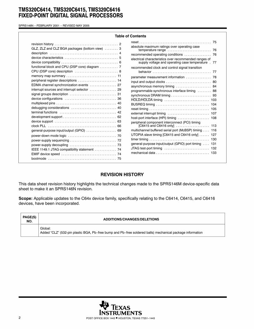
device characteristics Table 1 provides an overview of the C6414, C6415, and C6416 DSPs. The table shows significant features ofthe C64x devices, including the capacity of on-chip RAM, the peripherals, the CPU frequency, and the packagetype with pin count.
Table 1. Characteristics of the C6414, C6415, and C6416 ProcessorsHARDWARE FEATURES C6414, C6415, AND C6416
EMIFA (64-bit bus width)(default clock source = AECLKIN)
1
Peripherals EMIFB (16-bit bus width)(default clock source = BECLKIN)
1
Not all peripherals pinsare available at the
EDMA (64 independent channels) 1are available at thesame time. (For more HPI (32- or 16-bit user selectable) 1 (HPI16 or HPI32)same time. (For moredetails, see the Device PCI (32-bit) [DeviceID Register value 0xA106] 1 [C6415/C6416 only]details, see the DeviceConfiguration section.)
Peripheral performance
McBSPs (default internal clock source =CPU/4 clock frequency)
3
Peripheral performanceis dependent on UTOPIA (8-bit mode) 1 [C6415/C6416 only]is dependent onchip-level configuration. 32-Bit Timers (default internal clock source =
CPU/8 clock frequency)3
General-Purpose Input/Output 0 (GP0) 16
Decoder CoprocessorsVCP 1 (C6416 only)
Decoder CoprocessorsTCP 1 (C6416 only)
Size (Bytes) 1056K
On-Chip MemoryOrganization
16K-Byte (16KB) L1 Program (L1P) Cache16KB L1 Data (L1D) Cache1024KB Unified Mapped RAM/Cache (L2)
CPU ID + CPU Rev ID Control Status Register (CSR.[31:16]) 0x0C01
Device_IDSilicon Revision Identification Register (DEVICE_REV [19:16])Address: 0x01B0 0200
DEVICE_REV[19:16] Silicon Revision1111 1.03 or earlier0001 1.030010 or 0000 1.10011 2.0
Frequency MHz 500, 600, 720
Cycle Time ns
2 ns (C6414-5E0, C6415-5E0, C6416-5E0) and(C6414A-5E0, C6415A-5E0, C6416A-5E0)
[500-MHz CPU, 100-MHz EMIF]†
1.67 ns (C6414-6E3, C6415-6E3, C6416-6E3) and(C6414A-6E3, C6415A-6E3, C6416A-6E3)
[600-MHz CPU, 133-MHz EMIFA]† 1.39 ns (C6414-7E3, C6415-7E3, C6416-7E3)
[720-MHz CPU, 133-MHz EMIFA]†
VoltageCore (V)
1.2 V (-5E0)1.25 V (A-5E0)
1.4 V (-6E3, A-6E3, -7E3)
I/O (V) 3.3 V
PLL Options CLKIN frequency multiplier Bypass (x1), x6, x12
BGA Package 23 x 23 mm 532-Pin BGA (GLZ, ZLZ and CLZ)
Process Technology µm 0.13 µm
Product StatusProduct Preview (PP), Advance Information(AI), Production Data (PD)
PD‡
† On these C64x™ devices, the rated EMIF speed affects only the SDRAM interface on EMIFA. For more detailed information, see the EMIFDevice Speed section of this data sheet.
‡ All devices are now at the Production Data (PD) stage of development.

TMS320C6414, TMS320C6415, TMS320C6416FIXED-POINT DIGITAL SIGNAL PROCESSORS
SPRS146N − FEBRUARY 2001 − REVISED MAY 2005
6 POST OFFICE BOX 1443 • HOUSTON, TEXAS 77251−1443
device compatibility
The C64x™ generation of devices has a diverse and powerful set of peripherals. The common peripheral setand pin-compatibility that the C6414, C6415, and C6416 devices offer lead to easier system designs and fastertime to market. Table 2 identifies the peripherals and coprocessors that are available on the C6414, C6415, andC6416 devices.
The C6414, C6415, and C6416 devices are pin-for-pin compatible, provided the following conditions are met:
All devices are using the same peripherals. The C6414 is pin-for-pin compatible with the C6415/C6416 when the PCI and UTOPIA peripherals on theC6415/C6416 are disabled.The C6415 is pin-for-pin compatible with the C6416 when they are in the same peripheral selection mode.[For more information on peripheral selection, see the Device Configurations section of this data sheet.]
The BEA[9:7] pins are properly pulled up/down.[For more details on the device-specific BEA[9:7] pin configurations, see the Terminal Functions table ofthis data sheet.]
Table 2. Peripherals and Coprocessors Available on the C6414, C6415, and C6416 Devices†‡
PERIPHERALS/COPROCESSORS C6414 C6415 C6416
EMIFA (64-bit bus width) √ √ √
EMIFB (16-bit bus width) √ √ √
EDMA (64 independent channels) √ √ √
HPI (32- or 16-bit user selectable) √ √ √
PCI (32-bit) [Specification v2.2] — √ √
McBSPs (McBSP0, McBSP1, McBSP2) √ √ √
UTOPIA (8-bit mode) [Specification v1.0] — √ √
Timers (32-bit) [TIMER0, TIMER1, TIMER2] √ √ √
GPIOs (GP[15:0]) √ √ √
VCP/TCP Coprocessors — — √† — denotes peripheral/coprocessor is not available on this device.‡ Not all peripherals pins are available at the same time. (For more details, see the Device Configuration section.)
For more detailed information on the device compatibility and similarities/differences among the C6414, C6415,and C6416 devices, see the How To Begin Development Today With the TMS320C6414, TMS320C6415, andTMS320C6416 DSPs application report (literature number SPRA718).

TMS320C6414, TMS320C6415, TMS320C6416FIXED-POINT DIGITAL SIGNAL PROCESSORS
SPRS146N − FEBRUARY 2001 − REVISED MAY 2005
7POST OFFICE BOX 1443 • HOUSTON, TEXAS 77251−1443
functional block and CPU (DSP core) diagram
EMIF B16
64
Test
C64x DSP Core
Data Path B
B Register FileB31−B16B15−B0
Instruction Fetch
Instruction DispatchAdvanced Instruction Packet
Instruction Decode
Data Path A
A Register FileA31−A16A15−A0
Power-DownLogic
.L1 .S1 .M1 .D1 .D2 .M2 .S2 .L2
SDRAM
FIFO
SBSRAM
SRAM
L1P CacheDirect-Mapped16K Bytes Total
ControlRegisters
ControlLogic
L1D Cache2-Way Set-Associative
16K Bytes Total
AdvancedIn-CircuitEmulation
InterruptControl
McBSPs:Framing Chips:
H.100, MVIP,SCSA, T1, E1
AC97 Devices,SPI Devices,Codecs
C64x Digital Signal Processor
EnhancedDMA
Controller(64-channel)
32
L2Memory1024KBytes
PLL(x1, x6, x12)
Timer 2
EMIF A
McBSP1‡
McBSP0
HPI‡
ZBT SRAM
Timer 1
Timer 0
McBSP2
Boot Configuration
InterruptSelector
16
ROM/FLASH
I/O Devices
PCI‡
or
GPIO[8:0]
UTOPIA‡
or
GPIO[15:9]‡
UTOPIA:Up to 400 MbpsMaster ATMC
† VCP and TCP decoder coprocessors are applicable to the C6416 device only.‡ For the C6415 and C6416 devices, the UTOPIA peripheral is muxed with McBSP1, and the PCI peripheral is muxed with the HPI
peripheral and the GPIO[15:9] port. For more details on the multiplexed pins of these peripherals, see the Device Configurations sectionof this data sheet.
VCP†
TCP†

TMS320C6414, TMS320C6415, TMS320C6416FIXED-POINT DIGITAL SIGNAL PROCESSORS
SPRS146N − FEBRUARY 2001 − REVISED MAY 2005
8 POST OFFICE BOX 1443 • HOUSTON, TEXAS 77251−1443
CPU (DSP core) description
The CPU fetches VelociTI™ advanced very-long instruction words (VLIWs) (256 bits wide) to supply up to eight32-bit instructions to the eight functional units during every clock cycle. The VelociTI™ VLIW architecturefeatures controls by which all eight units do not have to be supplied with instructions if they are not ready toexecute. The first bit of every 32-bit instruction determines if the next instruction belongs to the same executepacket as the previous instruction, or whether it should be executed in the following clock as a part of the nextexecute packet. Fetch packets are always 256 bits wide; however, the execute packets can vary in size. Thevariable-length execute packets are a key memory-saving feature, distinguishing the C64x CPUs from otherVLIW architectures. The C64x™ VelociTI.2™ extensions add enhancements to the TMS320C62x™ DSPVelociTI™ architecture. These enhancements include:
Register file enhancements
Data path extensions
Quad 8-bit and dual 16-bit extensions with data flow enhancements
Additional functional unit hardware
Increased orthogonality of the instruction set
Additional instructions that reduce code size and increase register flexibility
The CPU features two sets of functional units. Each set contains four units and a register file. One set containsfunctional units .L1, .S1, .M1, and .D1; the other set contains units .D2, .M2, .S2, and .L2. The two register fileseach contain 32 32-bit registers for a total of 64 general-purpose registers. In addition to supporting the packed16-bit and 32-/40-bit fixed-point data types found in the C62x™ VelociTI™ VLIW architecture, the C64x™ registerfiles also support packed 8-bit data and 64-bit fixed-point data types. The two sets of functional units, along withtwo register files, compose sides A and B of the CPU [see the functional block and CPU (DSP core) diagram,and Figure 1]. The four functional units on each side of the CPU can freely share the 32 registers belonging tothat side. Additionally, each side features a “data cross path”—a single data bus connected to all the registerson the other side, by which the two sets of functional units can access data from the register files on the oppositeside. The C64x CPU pipelines data-cross-path accesses over multiple clock cycles. This allows the sameregister to be used as a data-cross-path operand by multiple functional units in the same execute packet. Allfunctional units in the C64x CPU can access operands via the data cross path. Register access by functionalunits on the same side of the CPU as the register file can service all the units in a single clock cycle. On the C64xCPU, a delay clock is introduced whenever an instruction attempts to read a register via a data cross path if thatregister was updated in the previous clock cycle.
In addition to the C62x™ DSP fixed-point instructions, the C64x™ DSP includes a comprehensive collection ofquad 8-bit and dual 16-bit instruction set extensions. These VelociTI.2™ extensions allow the C64x CPU tooperate directly on packed data to streamline data flow and increase instruction set efficiency.
Another key feature of the C64x CPU is the load/store architecture, where all instructions operate on registers(as opposed to data in memory). Two sets of data-addressing units (.D1 and .D2) are responsible for all datatransfers between the register files and the memory. The data address driven by the .D units allows dataaddresses generated from one register file to be used to load or store data to or from the other register file. TheC64x .D units can load and store bytes (8 bits), half-words (16 bits), and words (32 bits) with a single instruction.And with the new data path extensions, the C64x .D unit can load and store doublewords (64 bits) with a singleinstruction. Furthermore, the non-aligned load and store instructions allow the .D units to access words anddoublewords on any byte boundary. The C64x CPU supports a variety of indirect addressing modes using eitherlinear- or circular-addressing with 5- or 15-bit offsets. All instructions are conditional, and most can access anyone of the 64 registers. Some registers, however, are singled out to support specific addressing modes or tohold the condition for conditional instructions (if the condition is not automatically “true”).
TMS320C62x is a trademark of Texas Instruments.
TMS320C6414, TMS320C6415, TMS320C6416FIXED-POINT DIGITAL SIGNAL PROCESSORS
SPRS146N − FEBRUARY 2001 − REVISED MAY 2005
9POST OFFICE BOX 1443 • HOUSTON, TEXAS 77251−1443
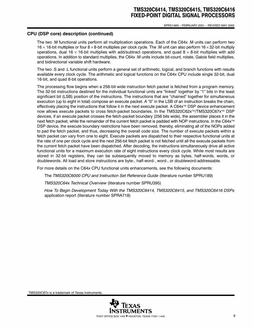
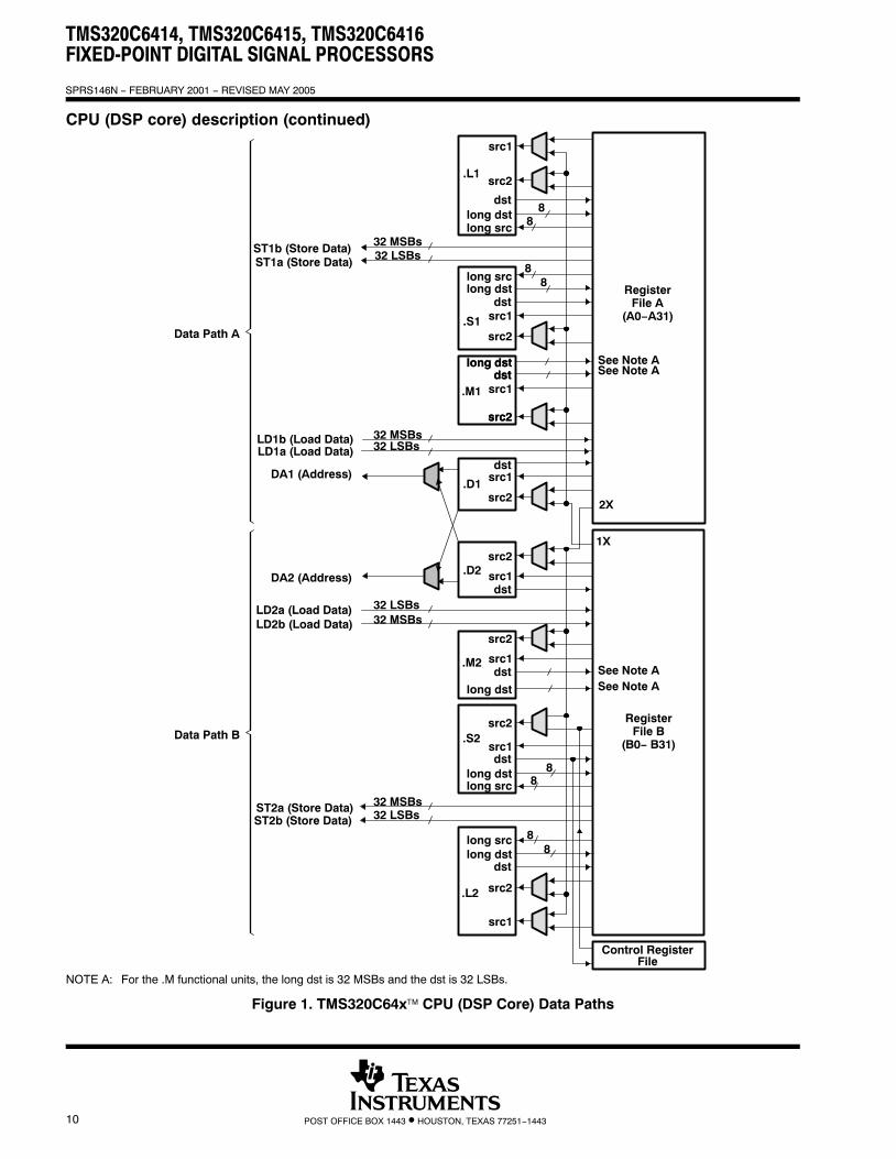
CPU (DSP core) description (continued)
The two .M functional units perform all multiplication operations. Each of the C64x .M units can perform two16 × 16-bit multiplies or four 8 × 8-bit multiplies per clock cycle. The .M unit can also perform 16 × 32-bit multiplyoperations, dual 16 × 16-bit multiplies with add/subtract operations, and quad 8 × 8-bit multiplies with addoperations. In addition to standard multiplies, the C64x .M units include bit-count, rotate, Galois field multiplies,and bidirectional variable shift hardware.
The two .S and .L functional units perform a general set of arithmetic, logical, and branch functions with resultsavailable every clock cycle. The arithmetic and logical functions on the C64x CPU include single 32-bit, dual16-bit, and quad 8-bit operations.
The processing flow begins when a 256-bit-wide instruction fetch packet is fetched from a program memory.The 32-bit instructions destined for the individual functional units are “linked” together by “1” bits in the leastsignificant bit (LSB) position of the instructions. The instructions that are “chained” together for simultaneousexecution (up to eight in total) compose an execute packet. A “0” in the LSB of an instruction breaks the chain,effectively placing the instructions that follow it in the next execute packet. A C64x™ DSP device enhancementnow allows execute packets to cross fetch-packet boundaries. In the TMS320C62x™/TMS320C67x™ DSPdevices, if an execute packet crosses the fetch-packet boundary (256 bits wide), the assembler places it in thenext fetch packet, while the remainder of the current fetch packet is padded with NOP instructions. In the C64x™DSP device, the execute boundary restrictions have been removed, thereby, eliminating all of the NOPs addedto pad the fetch packet, and thus, decreasing the overall code size. The number of execute packets within afetch packet can vary from one to eight. Execute packets are dispatched to their respective functional units atthe rate of one per clock cycle and the next 256-bit fetch packet is not fetched until all the execute packets fromthe current fetch packet have been dispatched. After decoding, the instructions simultaneously drive all activefunctional units for a maximum execution rate of eight instructions every clock cycle. While most results arestored in 32-bit registers, they can be subsequently moved to memory as bytes, half-words, words, ordoublewords. All load and store instructions are byte-, half-word-, word-, or doubleword-addressable.
For more details on the C64x CPU functional units enhancements, see the following documents:
The TMS320C6000 CPU and Instruction Set Reference Guide (literature number SPRU189)
TMS320C64x Technical Overview (literature number SPRU395)
How To Begin Development Today With the TMS320C6414, TMS320C6415, and TMS320C6416 DSPsapplication report (literature number SPRA718)
TMS320C67x is a trademark of Texas Instruments.
TMS320C6414, TMS320C6415, TMS320C6416FIXED-POINT DIGITAL SIGNAL PROCESSORS
SPRS146N − FEBRUARY 2001 − REVISED MAY 2005
10 POST OFFICE BOX 1443 • HOUSTON, TEXAS 77251−1443
CPU (DSP core) description (continued)
.L1
.S1
.M1
.D1
.D2
.M2
.S2
.L2
src1
long dst
88
src2
DA1 (Address)
ST1b (Store Data)
ST2a (Store Data)
RegisterFile A
(A0−A31)
88
88
dst
Data Path A
DA2 (Address)
RegisterFile B
(B0− B31)
LD2a (Load Data)
Data Path B
Control RegisterFile
ST2b (Store Data)
LD1b (Load Data)
88
2X
1X
ST1a (Store Data)
See Note ASee Note A
LD1a (Load Data)
LD2b (Load Data)
See Note ASee Note A
32 MSBs32 LSBs
32 MSBs32 LSBs
32 MSBs32 LSBs
32 MSBs32 LSBs
src2
src1
dstlong dstlong src
long srclong dst
dstsrc1
src2
src1
src2
src2
src1dst
src2
src1dst
src2
long dst
src2
src1dst
long dst
long dstlong src
long srclong dst
dst
dst
src2
src1
dst
NOTE A: For the .M functional units, the long dst is 32 MSBs and the dst is 32 LSBs.
Figure 1. TMS320C64x™ CPU (DSP Core) Data Paths
TMS320C6414, TMS320C6415, TMS320C6416FIXED-POINT DIGITAL SIGNAL PROCESSORS
SPRS146N − FEBRUARY 2001 − REVISED MAY 2005
11POST OFFICE BOX 1443 • HOUSTON, TEXAS 77251−1443
memory map summary
Table 3 shows the memory map address ranges of the TMS320C64x device. Internal memory is always locatedat address 0 and can be used as both program and data memory. The external memory address ranges in theC64x device begin at the hex address locations 0x6000 0000 for EMIFB and 0x8000 0000 for EMIFA.

TMS320C6414, TMS320C6415, TMS320C6416FIXED-POINT DIGITAL SIGNAL PROCESSORS
SPRS146N − FEBRUARY 2001 − REVISED MAY 2005
12 POST OFFICE BOX 1443 • HOUSTON, TEXAS 77251−1443
memory map summary (continued)
Table 3. TMS320C64x Memory Map Summary
MEMORY BLOCK DESCRIPTION BLOCK SIZE (BYTES) HEX ADDRESS RANGE
Internal RAM (L2) 1M 0000 0000 – 000F FFFF
Reserved 23M 0010 0000 – 017F FFFF
External Memory Interface A (EMIFA) Registers 256K 0180 0000 – 0183 FFFF
L2 Registers 256K 0184 0000 – 0187 FFFF
HPI Registers 256K 0188 0000 – 018B FFFF
McBSP 0 Registers 256K 018C 0000 – 018F FFFF
McBSP 1 Registers 256K 0190 0000 – 0193 FFFF
Timer 0 Registers 256K 0194 0000 – 0197 FFFF
Timer 1 Registers 256K 0198 0000 – 019B FFFF
Interrupt Selector Registers 256K 019C 0000 – 019F FFFF
EDMA RAM and EDMA Registers 256K 01A0 0000 – 01A3 FFFF
McBSP 2 Registers 256K 01A4 0000 – 01A7 FFFF
EMIFB Registers 256K 01A8 0000 – 01AB FFFF
Timer 2 Registers 256K 01AC 0000 – 01AF FFFF
GPIO Registers 256K 01B0 0000 – 01B3 FFFF
UTOPIA Registers (C6415 and C6416 only)† 256K 01B4 0000 – 01B7 FFFF
TCP/VCP Registers (C6416 only)‡ 256K 01B8 0000 – 01BB FFFF
Reserved 256K 01BC 0000 – 01BF FFFF
PCI Registers (C6415 and C6416 only)† 256K 01C0 0000 – 01C3 FFFF
Reserved 4M – 256K 01C4 0000 – 01FF FFFF
QDMA Registers 52 0200 0000 – 0200 0033
Reserved 736M – 52 0200 0034 – 2FFF FFFF
McBSP 0 Data 64M 3000 0000 – 33FF FFFF
McBSP 1 Data 64M 3400 0000 – 37FF FFFF
McBSP 2 Data 64M 3800 0000 – 3BFF FFFF
UTOPIA Queues (C6415 and C6416 only)† 64M 3C00 0000 – 3FFF FFFF
Reserved 256M 4000 0000 – 4FFF FFFF
TCP/VCP (C6416 only)‡ 256M 5000 0000 – 5FFF FFFF
EMIFB CE0 64M 6000 0000 – 63FF FFFF
EMIFB CE1 64M 6400 0000 – 67FF FFFF
EMIFB CE2 64M 6800 0000 – 6BFF FFFF
EMIFB CE3 64M 6C00 0000 – 6FFF FFFF
Reserved 256M 7000 0000 – 7FFF FFFF
EMIFA CE0 256M 8000 0000 – 8FFF FFFF
EMIFA CE1 256M 9000 0000 – 9FFF FFFF
EMIFA CE2 256M A000 0000 – AFFF FFFF
EMIFA CE3 256M B000 0000 – BFFF FFFF
Reserved 1G C000 0000 – FFFF FFFF† For the C6414 device, these memory address locations are reserved. The C6414 device does not support the UTOPIA and PCI peripherals.‡ Only the C6416 device supports the VCP/TCP Coprocessors. For the C6414 and C6415 devices, these memory address locations are reserved.
TMS320C6414, TMS320C6415, TMS320C6416FIXED-POINT DIGITAL SIGNAL PROCESSORS
SPRS146N − FEBRUARY 2001 − REVISED MAY 2005
13POST OFFICE BOX 1443 • HOUSTON, TEXAS 77251−1443
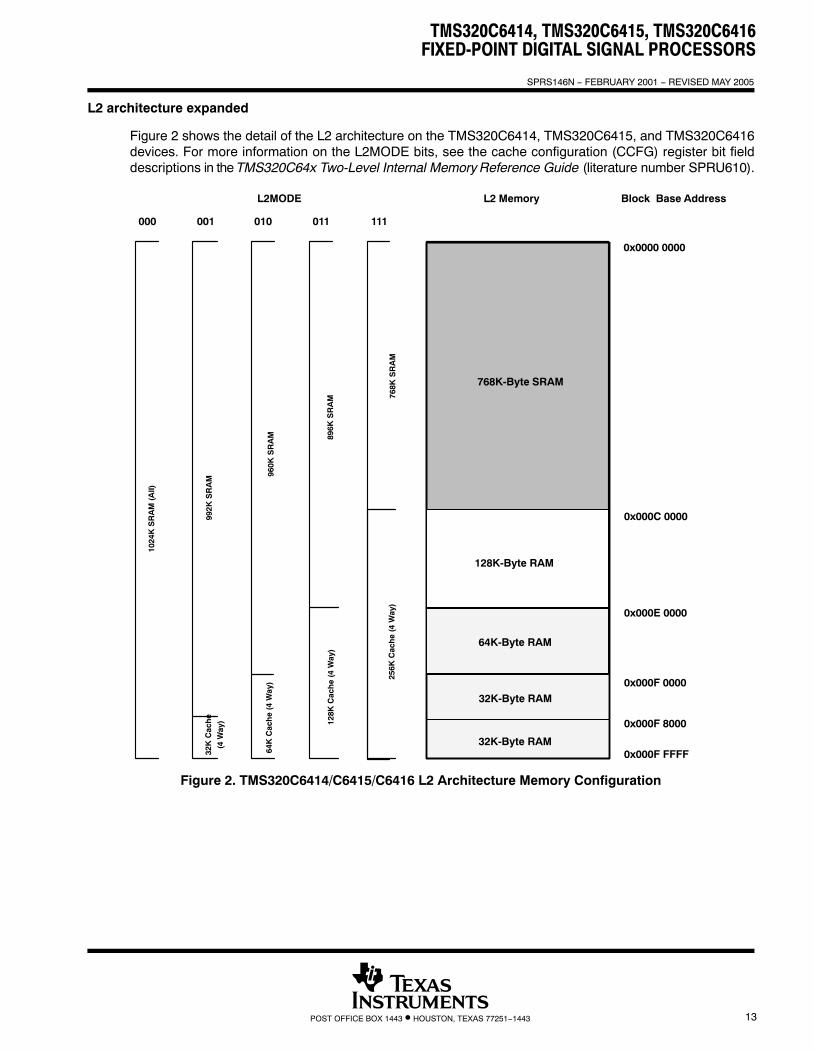
L2 architecture expanded
Figure 2 shows the detail of the L2 architecture on the TMS320C6414, TMS320C6415, and TMS320C6416devices. For more information on the L2MODE bits, see the cache configuration (CCFG) register bit fielddescriptions in the TMS320C64x Two-Level Internal Memory Reference Guide (literature number SPRU610).
ÎÎÎÎÎÎÎÎÎÎÎÎÎÎÎÎÎÎÎÎÎÎÎÎÎÎÎÎÎÎÎÎÎÎÎÎÎÎÎÎÎÎÎÎÎÎÎÎÎÎÎÎÎÎÎÎÎÎÎÎ
0x0000 0000
011010001 111
0x000C 0000
000
L2MODE L2 Memory Block Base Address
0x000F 0000
0x000E 0000
32K
Cac
he
(4 W
ay)
64K
Cac
he
(4 W
ay)
128K
Cac
he
(4 W
ay)
256K
Cac
he
(4 W
ay)
1024
K S
RA
M (
All)
992K
SR
AM
960K
SR
AM 89
6K S
RA
M
768K-Byte SRAM
128K-Byte RAM
32K-Byte RAM
0x000F FFFF
64K-Byte RAM
32K-Byte RAM
768K
SR
AM
0x000F 8000
Figure 2. TMS320C6414/C6415/C6416 L2 Architecture Memory Configuration

TMS320C6414, TMS320C6415, TMS320C6416FIXED-POINT DIGITAL SIGNAL PROCESSORS
SPRS146N − FEBRUARY 2001 − REVISED MAY 2005
14 POST OFFICE BOX 1443 • HOUSTON, TEXAS 77251−1443
peripheral register descriptions
Table 4 through Table 23 identify the peripheral registers for the C6414, C6415, and C6416 devices by theirregister names, acronyms, and hex address or hex address range. For more detailed information on the registercontents, bit names and their descriptions, see the specific peripheral reference guide listed in theTMS320C6000 DSP Peripherals Overview Reference Guide (literature number SPRU190).
Table 4. EMIFA Registers
HEX ADDRESS RANGE ACRONYM REGISTER NAME
0180 0000 GBLCTL EMIFA global control
0180 0004 CECTL1 EMIFA CE1 space control
0180 0008 CECTL0 EMIFA CE0 space control
0180 000C − Reserved
0180 0010 CECTL2 EMIFA CE2 space control
0180 0014 CECTL3 EMIFA CE3 space control
0180 0018 SDCTL EMIFA SDRAM control
0180 001C SDTIM EMIFA SDRAM refresh control
0180 0020 SDEXT EMIFA SDRAM extension
0180 0024 − 0180 003C − Reserved
0180 0040 PDTCTL Peripheral device transfer (PDT) control
0180 0044 CESEC1 EMIFA CE1 space secondary control
0180 0048 CESEC0 EMIFA CE0 space secondary control
0180 004C − Reserved
0180 0050 CESEC2 EMIFA CE2 space secondary control
0180 0054 CESEC3 EMIFA CE3 space secondary control
0180 0058 − 0183 FFFF – Reserved
Table 5. EMIFB Registers
HEX ADDRESS RANGE ACRONYM REGISTER NAME
01A8 0000 GBLCTL EMIFB global control
01A8 0004 CECTL1 EMIFB CE1 space control
01A8 0008 CECTL0 EMIFB CE0 space control
01A8 000C − Reserved
01A8 0010 CECTL2 EMIFB CE2 space control
01A8 0014 CECTL3 EMIFB CE3 space control
01A8 0018 SDCTL EMIFB SDRAM control
01A8 001C SDTIM EMIFB SDRAM refresh control
01A8 0020 SDEXT EMIFB SDRAM extension
01A8 0024 − 01A8 003C − Reserved
01A8 0040 PDTCTL Peripheral device transfer (PDT) control
01A8 0044 CESEC1 EMIFB CE1 space secondary control
01A8 0048 CESEC0 EMIFB CE0 space secondary control
01A8 004C − Reserved
01A8 0050 CESEC2 EMIFB CE2 space secondary control
01A8 0054 CESEC3 EMIFB CE3 space secondary control
01A8 0058 − 01AB FFFF – Reserved
TMS320C6414, TMS320C6415, TMS320C6416FIXED-POINT DIGITAL SIGNAL PROCESSORS
SPRS146N − FEBRUARY 2001 − REVISED MAY 2005
15POST OFFICE BOX 1443 • HOUSTON, TEXAS 77251−1443
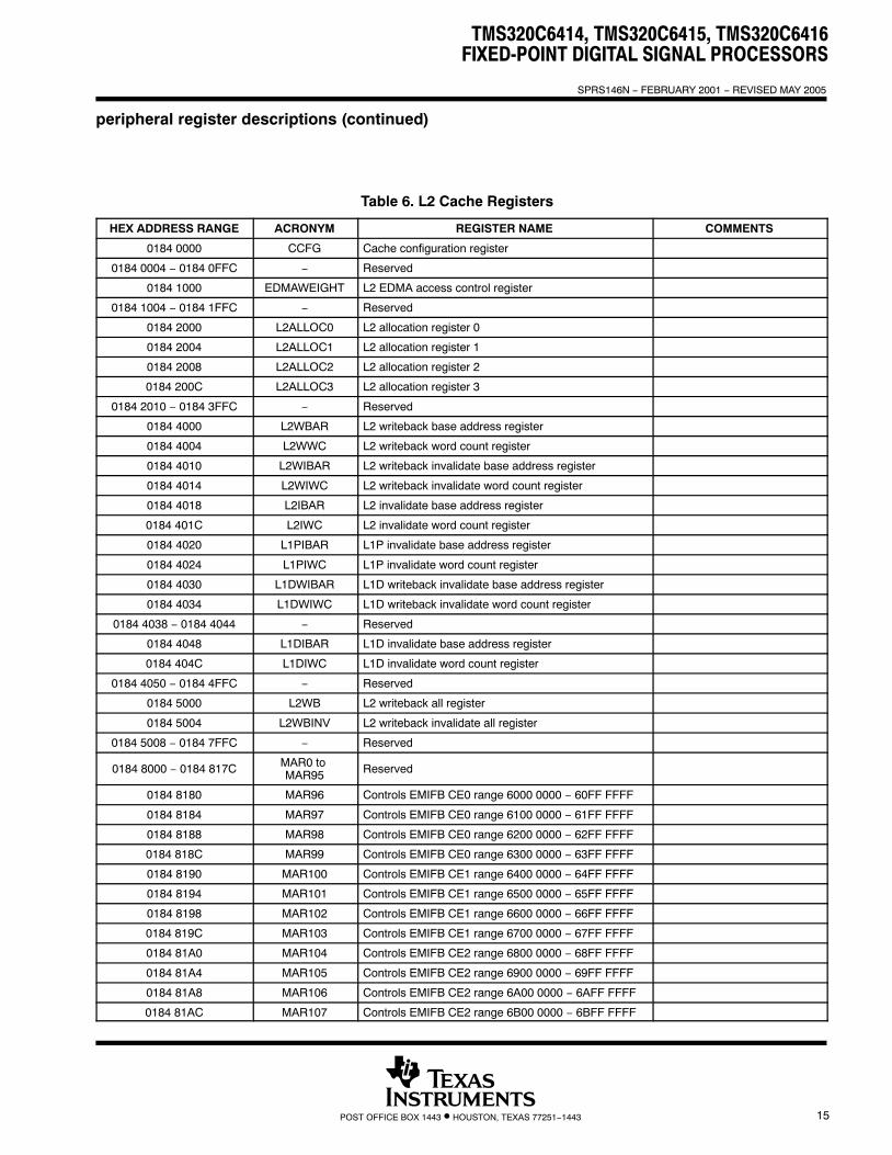
peripheral register descriptions (continued)
Table 6. L2 Cache Registers
HEX ADDRESS RANGE ACRONYM REGISTER NAME COMMENTS
0184 0000 CCFG Cache configuration register
0184 0004 − 0184 0FFC − Reserved
0184 1000 EDMAWEIGHT L2 EDMA access control register
0184 1004 − 0184 1FFC − Reserved
0184 2000 L2ALLOC0 L2 allocation register 0
0184 2004 L2ALLOC1 L2 allocation register 1
0184 2008 L2ALLOC2 L2 allocation register 2
0184 200C L2ALLOC3 L2 allocation register 3
0184 2010 − 0184 3FFC − Reserved
0184 4000 L2WBAR L2 writeback base address register
0184 4004 L2WWC L2 writeback word count register
0184 4010 L2WIBAR L2 writeback invalidate base address register
0184 4014 L2WIWC L2 writeback invalidate word count register
0184 4018 L2IBAR L2 invalidate base address register
0184 401C L2IWC L2 invalidate word count register
0184 4020 L1PIBAR L1P invalidate base address register
0184 4024 L1PIWC L1P invalidate word count register
0184 4030 L1DWIBAR L1D writeback invalidate base address register
0184 4034 L1DWIWC L1D writeback invalidate word count register
0184 4038 − 0184 4044 − Reserved
0184 4048 L1DIBAR L1D invalidate base address register
0184 404C L1DIWC L1D invalidate word count register
0184 4050 − 0184 4FFC − Reserved
0184 5000 L2WB L2 writeback all register
0184 5004 L2WBINV L2 writeback invalidate all register
0184 5008 − 0184 7FFC − Reserved
0184 8000 − 0184 817C MAR0 to MAR95 Reserved
0184 8180 MAR96 Controls EMIFB CE0 range 6000 0000 − 60FF FFFF
0184 8184 MAR97 Controls EMIFB CE0 range 6100 0000 − 61FF FFFF
0184 8188 MAR98 Controls EMIFB CE0 range 6200 0000 − 62FF FFFF
0184 818C MAR99 Controls EMIFB CE0 range 6300 0000 − 63FF FFFF
0184 8190 MAR100 Controls EMIFB CE1 range 6400 0000 − 64FF FFFF
0184 8194 MAR101 Controls EMIFB CE1 range 6500 0000 − 65FF FFFF
0184 8198 MAR102 Controls EMIFB CE1 range 6600 0000 − 66FF FFFF
0184 819C MAR103 Controls EMIFB CE1 range 6700 0000 − 67FF FFFF
0184 81A0 MAR104 Controls EMIFB CE2 range 6800 0000 − 68FF FFFF
0184 81A4 MAR105 Controls EMIFB CE2 range 6900 0000 − 69FF FFFF
0184 81A8 MAR106 Controls EMIFB CE2 range 6A00 0000 − 6AFF FFFF
0184 81AC MAR107 Controls EMIFB CE2 range 6B00 0000 − 6BFF FFFF
TMS320C6414, TMS320C6415, TMS320C6416FIXED-POINT DIGITAL SIGNAL PROCESSORS
SPRS146N − FEBRUARY 2001 − REVISED MAY 2005
16 POST OFFICE BOX 1443 • HOUSTON, TEXAS 77251−1443
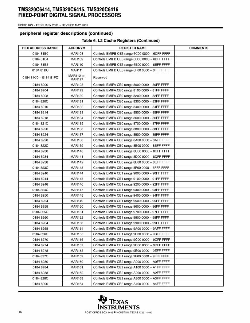
Table 6. L2 Cache Registers (Continued)
HEX ADDRESS RANGE COMMENTSREGISTER NAMEACRONYM
0184 81B0 MAR108 Controls EMIFB CE3 range 6C00 0000 − 6CFF FFFF
0184 81B4 MAR109 Controls EMIFB CE3 range 6D00 0000 − 6DFF FFFF
0184 81B8 MAR110 Controls EMIFB CE3 range 6E00 0000 − 6EFF FFFF
0184 81BC MAR111 Controls EMIFB CE3 range 6F00 0000 − 6FFF FFFF
0184 81C0 − 0184 81FC MAR112 to MAR127 Reserved
0184 8200 MAR128 Controls EMIFA CE0 range 8000 0000 − 80FF FFFF
0184 8204 MAR129 Controls EMIFA CE0 range 8100 0000 − 81FF FFFF
0184 8208 MAR130 Controls EMIFA CE0 range 8200 0000 − 82FF FFFF
0184 820C MAR131 Controls EMIFA CE0 range 8300 0000 − 83FF FFFF
0184 8210 MAR132 Controls EMIFA CE0 range 8400 0000 − 84FF FFFF
0184 8214 MAR133 Controls EMIFA CE0 range 8500 0000 − 85FF FFFF
0184 8218 MAR134 Controls EMIFA CE0 range 8600 0000 − 86FF FFFF
0184 821C MAR135 Controls EMIFA CE0 range 8700 0000 − 87FF FFFF
0184 8220 MAR136 Controls EMIFA CE0 range 8800 0000 − 88FF FFFF
0184 8224 MAR137 Controls EMIFA CE0 range 8900 0000 − 89FF FFFF
0184 8228 MAR138 Controls EMIFA CE0 range 8A00 0000 − 8AFF FFFF
0184 822C MAR139 Controls EMIFA CE0 range 8B00 0000 − 8BFF FFFF
0184 8230 MAR140 Controls EMIFA CE0 range 8C00 0000 − 8CFF FFFF
0184 8234 MAR141 Controls EMIFA CE0 range 8D00 0000 − 8DFF FFFF
0184 8238 MAR142 Controls EMIFA CE0 range 8E00 0000 − 8EFF FFFF
0184 823C MAR143 Controls EMIFA CE0 range 8F00 0000 − 8FFF FFFF
0184 8240 MAR144 Controls EMIFA CE1 range 9000 0000 − 90FF FFFF
0184 8244 MAR145 Controls EMIFA CE1 range 9100 0000 − 91FF FFFF
0184 8248 MAR146 Controls EMIFA CE1 range 9200 0000 − 92FF FFFF
0184 824C MAR147 Controls EMIFA CE1 range 9300 0000 − 93FF FFFF
0184 8250 MAR148 Controls EMIFA CE1 range 9400 0000 − 94FF FFFF
0184 8254 MAR149 Controls EMIFA CE1 range 9500 0000 − 95FF FFFF
0184 8258 MAR150 Controls EMIFA CE1 range 9600 0000 − 96FF FFFF
0184 825C MAR151 Controls EMIFA CE1 range 9700 0000 − 97FF FFFF
0184 8260 MAR152 Controls EMIFA CE1 range 9800 0000 − 98FF FFFF
0184 8264 MAR153 Controls EMIFA CE1 range 9900 0000 − 99FF FFFF
0184 8268 MAR154 Controls EMIFA CE1 range 9A00 0000 − 9AFF FFFF
0184 826C MAR155 Controls EMIFA CE1 range 9B00 0000 − 9BFF FFFF
0184 8270 MAR156 Controls EMIFA CE1 range 9C00 0000 − 9CFF FFFF
0184 8274 MAR157 Controls EMIFA CE1 range 9D00 0000 − 9DFF FFFF
0184 8278 MAR158 Controls EMIFA CE1 range 9E00 0000 − 9EFF FFFF
0184 827C MAR159 Controls EMIFA CE1 range 9F00 0000 − 9FFF FFFF
0184 8280 MAR160 Controls EMIFA CE2 range A000 0000 − A0FF FFFF
0184 8284 MAR161 Controls EMIFA CE2 range A100 0000 − A1FF FFFF
0184 8288 MAR162 Controls EMIFA CE2 range A200 0000 − A2FF FFFF
0184 828C MAR163 Controls EMIFA CE2 range A300 0000 − A3FF FFFF
0184 8290 MAR164 Controls EMIFA CE2 range A400 0000 − A4FF FFFF
peripheral register descriptions (continued)
TMS320C6414, TMS320C6415, TMS320C6416FIXED-POINT DIGITAL SIGNAL PROCESSORS
SPRS146N − FEBRUARY 2001 − REVISED MAY 2005
17POST OFFICE BOX 1443 • HOUSTON, TEXAS 77251−1443
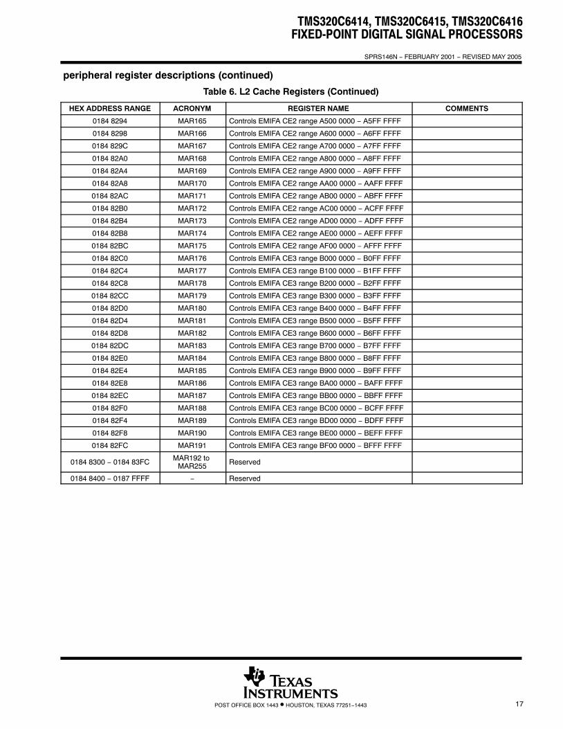
Table 6. L2 Cache Registers (Continued)
HEX ADDRESS RANGE COMMENTSREGISTER NAMEACRONYM
0184 8294 MAR165 Controls EMIFA CE2 range A500 0000 − A5FF FFFF
0184 8298 MAR166 Controls EMIFA CE2 range A600 0000 − A6FF FFFF
0184 829C MAR167 Controls EMIFA CE2 range A700 0000 − A7FF FFFF
0184 82A0 MAR168 Controls EMIFA CE2 range A800 0000 − A8FF FFFF
0184 82A4 MAR169 Controls EMIFA CE2 range A900 0000 − A9FF FFFF
0184 82A8 MAR170 Controls EMIFA CE2 range AA00 0000 − AAFF FFFF
0184 82AC MAR171 Controls EMIFA CE2 range AB00 0000 − ABFF FFFF
0184 82B0 MAR172 Controls EMIFA CE2 range AC00 0000 − ACFF FFFF
0184 82B4 MAR173 Controls EMIFA CE2 range AD00 0000 − ADFF FFFF
0184 82B8 MAR174 Controls EMIFA CE2 range AE00 0000 − AEFF FFFF
0184 82BC MAR175 Controls EMIFA CE2 range AF00 0000 − AFFF FFFF
0184 82C0 MAR176 Controls EMIFA CE3 range B000 0000 − B0FF FFFF
0184 82C4 MAR177 Controls EMIFA CE3 range B100 0000 − B1FF FFFF
0184 82C8 MAR178 Controls EMIFA CE3 range B200 0000 − B2FF FFFF
0184 82CC MAR179 Controls EMIFA CE3 range B300 0000 − B3FF FFFF
0184 82D0 MAR180 Controls EMIFA CE3 range B400 0000 − B4FF FFFF
0184 82D4 MAR181 Controls EMIFA CE3 range B500 0000 − B5FF FFFF
0184 82D8 MAR182 Controls EMIFA CE3 range B600 0000 − B6FF FFFF
0184 82DC MAR183 Controls EMIFA CE3 range B700 0000 − B7FF FFFF
0184 82E0 MAR184 Controls EMIFA CE3 range B800 0000 − B8FF FFFF
0184 82E4 MAR185 Controls EMIFA CE3 range B900 0000 − B9FF FFFF
0184 82E8 MAR186 Controls EMIFA CE3 range BA00 0000 − BAFF FFFF
0184 82EC MAR187 Controls EMIFA CE3 range BB00 0000 − BBFF FFFF
0184 82F0 MAR188 Controls EMIFA CE3 range BC00 0000 − BCFF FFFF
0184 82F4 MAR189 Controls EMIFA CE3 range BD00 0000 − BDFF FFFF
0184 82F8 MAR190 Controls EMIFA CE3 range BE00 0000 − BEFF FFFF
0184 82FC MAR191 Controls EMIFA CE3 range BF00 0000 − BFFF FFFF
0184 8300 − 0184 83FC MAR192 to MAR255 Reserved
0184 8400 − 0187 FFFF − Reserved
peripheral register descriptions (continued)

TMS320C6414, TMS320C6415, TMS320C6416FIXED-POINT DIGITAL SIGNAL PROCESSORS
SPRS146N − FEBRUARY 2001 − REVISED MAY 2005
18 POST OFFICE BOX 1443 • HOUSTON, TEXAS 77251−1443
peripheral register descriptions (continued)
Table 7. EDMA Registers
HEX ADDRESS RANGE ACRONYM REGISTER NAME
01A0 FF9C EPRH Event polarity high register
01A0 FFA4 CIPRH Channel interrupt pending high register
01A0 FFA8 CIERH Channel interrupt enable high register
01A0 FFAC CCERH Channel chain enable high register
01A0 FFB0 ERH Event high register
01A0 FFB4 EERH Event enable high register
01A0 FFB8 ECRH Event clear high register
01A0 FFBC ESRH Event set high register
01A0 FFC0 PQAR0 Priority queue allocation register 0
01A0 FFC4 PQAR1 Priority queue allocation register 1
01A0 FFC8 PQAR2 Priority queue allocation register 2
01A0 FFCC PQAR3 Priority queue allocation register 3
01A0 FFDC EPRL Event polarity low register
01A0 FFE0 PQSR Priority queue status register
01A0 FFE4 CIPRL Channel interrupt pending low register
01A0 FFE8 CIERL Channel interrupt enable low register
01A0 FFEC CCERL Channel chain enable low register
01A0 FFF0 ERL Event low register
01A0 FFF4 EERL Event enable low register
01A0 FFF8 ECRL Event clear low register
01A0 FFFC ESRL Event set low register
01A1 0000 − 01A3 FFFF – Reserved

TMS320C6414, TMS320C6415, TMS320C6416FIXED-POINT DIGITAL SIGNAL PROCESSORS
SPRS146N − FEBRUARY 2001 − REVISED MAY 2005
19POST OFFICE BOX 1443 • HOUSTON, TEXAS 77251−1443
peripheral register descriptions (continued)
Table 8. EDMA Parameter RAM†
HEX ADDRESS RANGE ACRONYM REGISTER NAME COMMENTS
01A0 0000 − 01A0 0017 − Parameters for Event 0 (6 words)
01A0 0018 − 01A0 002F − Parameters for Event 1 (6 words)
01A0 0030 − 01A0 0047 − Parameters for Event 2 (6 words)
01A0 0048 − 01A0 005F − Parameters for Event 3 (6 words)
01A0 0060 − 01A0 0077 − Parameters for Event 4 (6 words)
01A0 0078 − 01A0 008F − Parameters for Event 5 (6 words)
01A0 0090 − 01A0 00A7 − Parameters for Event 6 (6 words)
01A0 00A8 − 01A0 00BF − Parameters for Event 7 (6 words)
01A0 00C0 − 01A0 00D7 − Parameters for Event 8 (6 words)
01A0 00D8 − 01A0 00EF − Parameters for Event 9 (6 words)
01A0 00F0 − 01A0 00107 − Parameters for Event 10 (6 words)
01A0 0108 − 01A0 011F − Parameters for Event 11 (6 words)
01A0 0120 − 01A0 0137 − Parameters for Event 12 (6 words)
01A0 0138 − 01A0 014F − Parameters for Event 13 (6 words)
01A0 0150 − 01A0 0167 − Parameters for Event 14 (6 words)
01A0 0168 − 01A0 017F − Parameters for Event 15 (6 words)
01A0 0150 − 01A0 0167 − Parameters for Event 16 (6 words)
01A0 0168 − 01A0 017F − Parameters for Event 17 (6 words)
... ...
... ...
01A0 05D0 − 01A0 05E7 − Parameters for Event 62 (6 words)
01A0 05E8 − 01A0 05FF − Parameters for Event 63 (6 words)
01A0 0600 − 01A0 0617 − Reload/link parameters for Event M (6 words)
01A0 0618 − 01A0 062F − Reload/link parameters for Event N (6 words)
... ...
01A0 07E0 − 01A0 07F7 − Reload/link parameters for Event Z (6 words)
01A0 07F8 − 01A0 07FF − Scratch pad area (2 words)† The C6414/C6415/C6416 device has twenty-one parameter sets [six (6) words each] that can be used to reload/link EDMA transfers.
Table 9. Quick DMA (QDMA) and Pseudo Registers
HEX ADDRESS RANGE ACRONYM REGISTER NAME
0200 0000 QOPT QDMA options parameter register
0200 0004 QSRC QDMA source address register
0200 0008 QCNT QDMA frame count register
0200 000C QDST QDMA destination address register
0200 0010 QIDX QDMA index register
0200 0014 − 0200 001C Reserved
0200 0020 QSOPT QDMA pseudo options register
0200 0024 QSSRC QDMA pseudo source address register
0200 0028 QSCNT QDMA pseudo frame count register
0200 002C QSDST QDMA pseudo destination address register
0200 0030 QSIDX QDMA pseudo index register
TMS320C6414, TMS320C6415, TMS320C6416FIXED-POINT DIGITAL SIGNAL PROCESSORS
SPRS146N − FEBRUARY 2001 − REVISED MAY 2005
20 POST OFFICE BOX 1443 • HOUSTON, TEXAS 77251−1443
peripheral register descriptions (continued)
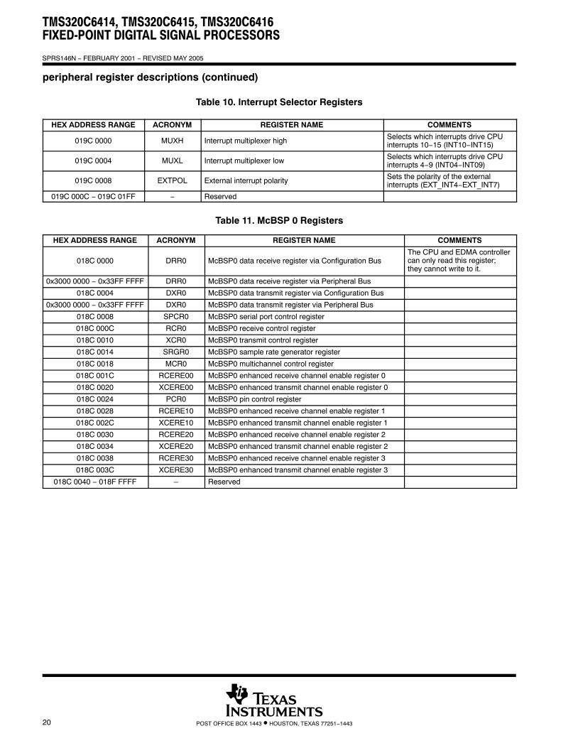
Table 10. Interrupt Selector Registers
HEX ADDRESS RANGE ACRONYM REGISTER NAME COMMENTS
019C 0000 MUXH Interrupt multiplexer high Selects which interrupts drive CPUinterrupts 10−15 (INT10−INT15)
019C 0004 MUXL Interrupt multiplexer low Selects which interrupts drive CPUinterrupts 4−9 (INT04−INT09)
019C 0008 EXTPOL External interrupt polarity Sets the polarity of the externalinterrupts (EXT_INT4−EXT_INT7)
019C 000C − 019C 01FF − Reserved
Table 11. McBSP 0 Registers
HEX ADDRESS RANGE ACRONYM REGISTER NAME COMMENTS
018C 0000 DRR0 McBSP0 data receive register via Configuration BusThe CPU and EDMA controllercan only read this register;they cannot write to it.
0x3000 0000 − 0x33FF FFFF DRR0 McBSP0 data receive register via Peripheral Bus
018C 0004 DXR0 McBSP0 data transmit register via Configuration Bus
0x3000 0000 − 0x33FF FFFF DXR0 McBSP0 data transmit register via Peripheral Bus
018C 0008 SPCR0 McBSP0 serial port control register
018C 000C RCR0 McBSP0 receive control register
018C 0010 XCR0 McBSP0 transmit control register
018C 0014 SRGR0 McBSP0 sample rate generator register
018C 0018 MCR0 McBSP0 multichannel control register
018C 001C RCERE00 McBSP0 enhanced receive channel enable register 0
018C 0020 XCERE00 McBSP0 enhanced transmit channel enable register 0
018C 0024 PCR0 McBSP0 pin control register
018C 0028 RCERE10 McBSP0 enhanced receive channel enable register 1
018C 002C XCERE10 McBSP0 enhanced transmit channel enable register 1
018C 0030 RCERE20 McBSP0 enhanced receive channel enable register 2
018C 0034 XCERE20 McBSP0 enhanced transmit channel enable register 2
018C 0038 RCERE30 McBSP0 enhanced receive channel enable register 3
018C 003C XCERE30 McBSP0 enhanced transmit channel enable register 3
018C 0040 − 018F FFFF – Reserved
TMS320C6414, TMS320C6415, TMS320C6416FIXED-POINT DIGITAL SIGNAL PROCESSORS
SPRS146N − FEBRUARY 2001 − REVISED MAY 2005
21POST OFFICE BOX 1443 • HOUSTON, TEXAS 77251−1443
peripheral register descriptions (continued)
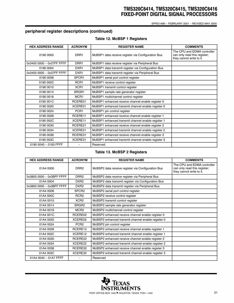
Table 12. McBSP 1 Registers
HEX ADDRESS RANGE ACRONYM REGISTER NAME COMMENTS
0190 0000 DRR1 McBSP1 data receive register via Configuration BusThe CPU and EDMA controllercan only read this register;they cannot write to it.
0x3400 0000 − 0x37FF FFFF DRR1 McBSP1 data receive register via Peripheral Bus
0190 0004 DXR1 McBSP1 data transmit register via Configuration Bus
0x3400 0000 − 0x37FF FFFF DXR1 McBSP1 data transmit register via Peripheral Bus
0190 0008 SPCR1 McBSP1 serial port control register
0190 000C RCR1 McBSP1 receive control register
0190 0010 XCR1 McBSP1 transmit control register
0190 0014 SRGR1 McBSP1 sample rate generator register
0190 0018 MCR1 McBSP1 multichannel control register
0190 001C RCERE01 McBSP1 enhanced receive channel enable register 0
0190 0020 XCERE01 McBSP1 enhanced transmit channel enable register 0
0190 0024 PCR1 McBSP1 pin control register
0190 0028 RCERE11 McBSP1 enhanced receive channel enable register 1
0190 002C XCERE11 McBSP1 enhanced transmit channel enable register 1
0190 0030 RCERE21 McBSP1 enhanced receive channel enable register 2
0190 0034 XCERE21 McBSP1 enhanced transmit channel enable register 2
0190 0038 RCERE31 McBSP1 enhanced receive channel enable register 3
0190 003C XCERE31 McBSP1 enhanced transmit channel enable register 3
0190 0040 − 0193 FFFF – Reserved
Table 13. McBSP 2 Registers
HEX ADDRESS RANGE ACRONYM REGISTER NAME COMMENTS
01A4 0000 DRR2 McBSP2 data receive register via Configuration BusThe CPU and EDMA controllercan only read this register;they cannot write to it.
0x3800 0000 − 0x3BFF FFFF DRR2 McBSP2 data receive register via Peripheral Bus
01A4 0004 DXR2 McBSP2 data transmit register via Configuration Bus
0x3800 0000 − 0x3BFF FFFF DXR2 McBSP2 data transmit register via Peripheral Bus
01A4 0008 SPCR2 McBSP2 serial port control register
01A4 000C RCR2 McBSP2 receive control register
01A4 0010 XCR2 McBSP2 transmit control register
01A4 0014 SRGR2 McBSP2 sample rate generator register
01A4 0018 MCR2 McBSP2 multichannel control register
01A4 001C RCERE02 McBSP2 enhanced receive channel enable register 0
01A4 0020 XCERE02 McBSP2 enhanced transmit channel enable register 0
01A4 0024 PCR2 McBSP2 pin control register
01A4 0028 RCERE12 McBSP2 enhanced receive channel enable register 1
01A4 002C XCERE12 McBSP2 enhanced transmit channel enable register 1
01A4 0030 RCERE22 McBSP2 enhanced receive channel enable register 2
01A4 0034 XCERE22 McBSP2 enhanced transmit channel enable register 2
01A4 0038 RCERE32 McBSP2 enhanced receive channel enable register 3
01A4 003C XCERE32 McBSP2 enhanced transmit channel enable register 3
01A4 0040 − 01A7 FFFF – Reserved
TMS320C6414, TMS320C6415, TMS320C6416FIXED-POINT DIGITAL SIGNAL PROCESSORS
SPRS146N − FEBRUARY 2001 − REVISED MAY 2005
22 POST OFFICE BOX 1443 • HOUSTON, TEXAS 77251−1443
peripheral register descriptions (continued)
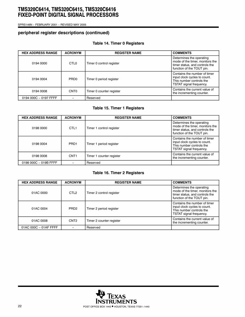
Table 14. Timer 0 Registers
HEX ADDRESS RANGE ACRONYM REGISTER NAME COMMENTS
0194 0000 CTL0 Timer 0 control register
Determines the operatingmode of the timer, monitors thetimer status, and controls thefunction of the TOUT pin.
0194 0004 PRD0 Timer 0 period register
Contains the number of timerinput clock cycles to count.This number controls theTSTAT signal frequency.
0194 0008 CNT0 Timer 0 counter register Contains the current value ofthe incrementing counter.
0194 000C − 0197 FFFF − Reserved
Table 15. Timer 1 Registers
HEX ADDRESS RANGE ACRONYM REGISTER NAME COMMENTS
0198 0000 CTL1 Timer 1 control register
Determines the operatingmode of the timer, monitors thetimer status, and controls thefunction of the TOUT pin.
0198 0004 PRD1 Timer 1 period register
Contains the number of timerinput clock cycles to count.This number controls theTSTAT signal frequency.
0198 0008 CNT1 Timer 1 counter register Contains the current value ofthe incrementing counter.
0198 000C − 019B FFFF − Reserved
Table 16. Timer 2 Registers
HEX ADDRESS RANGE ACRONYM REGISTER NAME COMMENTS
01AC 0000 CTL2 Timer 2 control register
Determines the operatingmode of the timer, monitors thetimer status, and controls thefunction of the TOUT pin.
01AC 0004 PRD2 Timer 2 period register
Contains the number of timerinput clock cycles to count.This number controls theTSTAT signal frequency.
01AC 0008 CNT2 Timer 2 counter register Contains the current value ofthe incrementing counter.
01AC 000C − 01AF FFFF − Reserved

TMS320C6414, TMS320C6415, TMS320C6416FIXED-POINT DIGITAL SIGNAL PROCESSORS
SPRS146N − FEBRUARY 2001 − REVISED MAY 2005
23POST OFFICE BOX 1443 • HOUSTON, TEXAS 77251−1443
peripheral register descriptions (continued)
Table 17. HPI Registers
HEX ADDRESS RANGE ACRONYM REGISTER NAME COMMENTS
− HPID HPI data register Host read/write access only
0188 0000 HPIC HPI control register HPIC has both Host/CPUread/write access
0188 0004 HPIA(HPIAW)† HPI address register (Write)
HPIA has both Host/CPU
0188 0008 HPIA(HPIAR)† HPI address register (Read)
HPIA has both Host/CPUread/write access
0188 000C − 0189 FFFF − Reserved
018A 0000 TRCTL HPI transfer request control register
018A 0004 − 018B FFFF − Reserved† Host access to the HPIA register updates both the HPIAW and HPIAR registers. The CPU can access HPIAW and HPIAR independently.
Table 18. GPIO Registers
HEX ADDRESS RANGE ACRONYM REGISTER NAME
01B0 0000 GPEN GPIO enable register
01B0 0004 GPDIR GPIO direction register
01B0 0008 GPVAL GPIO value register
01B0 000C − Reserved
01B0 0010 GPDH GPIO delta high register
01B0 0014 GPHM GPIO high mask register
01B0 0018 GPDL GPIO delta low register
01B0 001C GPLM GPIO low mask register
01B0 0020 GPGC GPIO global control register
01B0 0024 GPPOL GPIO interrupt polarity register
01B0 0028 − 01B0 01FF − Reserved
01B0 0200 DEVICE_REVSilicon Revision Identification Register(For more details, see the device characteristics listed in Table 1.)
01B0 0204 − 01B3 FFFF − Reserved
TMS320C6414, TMS320C6415, TMS320C6416FIXED-POINT DIGITAL SIGNAL PROCESSORS
SPRS146N − FEBRUARY 2001 − REVISED MAY 2005
24 POST OFFICE BOX 1443 • HOUSTON, TEXAS 77251−1443
peripheral register descriptions (continued)
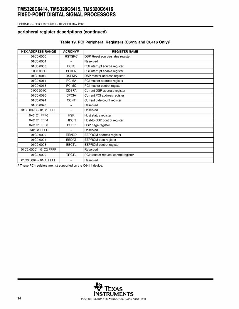
Table 19. PCI Peripheral Registers (C6415 and C6416 Only)†
HEX ADDRESS RANGE ACRONYM REGISTER NAME
01C0 0000 RSTSRC DSP Reset source/status register
01C0 0004 − Reserved
01C0 0008 PCIIS PCI interrupt source register
01C0 000C PCIIEN PCI interrupt enable register
01C0 0010 DSPMA DSP master address register
01C0 0014 PCIMA PCI master address register
01C0 0018 PCIMC PCI master control register
01C0 001C CDSPA Current DSP address register
01C0 0020 CPCIA Current PCI address register
01C0 0024 CCNT Current byte count register
01C0 0028 − Reserved
01C0 002C − 01C1 FFEF – Reserved
0x01C1 FFF0 HSR Host status register
0x01C1 FFF4 HDCR Host-to-DSP control register
0x01C1 FFF8 DSPP DSP page register
0x01C1 FFFC − Reserved
01C2 0000 EEADD EEPROM address register
01C2 0004 EEDAT EEPROM data register
01C2 0008 EECTL EEPROM control register
01C2 000C − 01C2 FFFF – Reserved
01C3 0000 TRCTL PCI transfer request control register
01C3 0004 − 01C3 FFFF – Reserved† These PCI registers are not supported on the C6414 device.
TMS320C6414, TMS320C6415, TMS320C6416FIXED-POINT DIGITAL SIGNAL PROCESSORS
SPRS146N − FEBRUARY 2001 − REVISED MAY 2005
25POST OFFICE BOX 1443 • HOUSTON, TEXAS 77251−1443
peripheral register descriptions (continued)
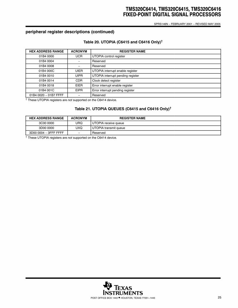
Table 20. UTOPIA (C6415 and C6416 Only)†
HEX ADDRESS RANGE ACRONYM REGISTER NAME
01B4 0000 UCR UTOPIA control register
01B4 0004 − Reserved
01B4 0008 − Reserved
01B4 000C UIER UTOPIA interrupt enable register
01B4 0010 UIPR UTOPIA interrupt pending register
01B4 0014 CDR Clock detect register
01B4 0018 EIER Error interrupt enable register
01B4 001C EIPR Error interrupt pending register
01B4 0020 − 01B7 FFFF − Reserved† These UTOPIA registers are not supported on the C6414 device.
Table 21. UTOPIA QUEUES (C6415 and C6416 Only)†
HEX ADDRESS RANGE ACRONYM REGISTER NAME
3C00 0000 URQ UTOPIA receive queue
3D00 0000 UXQ UTOPIA transmit queue
3D00 0004 − 3FFF FFFF − Reserved† These UTOPIA registers are not supported on the C6414 device.
TMS320C6414, TMS320C6415, TMS320C6416FIXED-POINT DIGITAL SIGNAL PROCESSORS
SPRS146N − FEBRUARY 2001 − REVISED MAY 2005
26 POST OFFICE BOX 1443 • HOUSTON, TEXAS 77251−1443
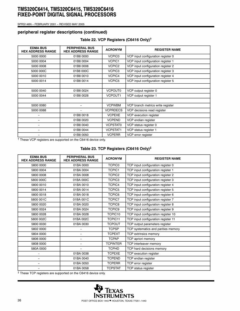
peripheral register descriptions (continued)
Table 22. VCP Registers (C6416 Only)†
EDMA BUS HEX ADDRESS RANGE
PERIPHERAL BUS HEX ADDRESS RANGE ACRONYM REGISTER NAME
5000 0000 01B8 0000 VCPIC0 VCP input configuration register 0
5000 0004 01B8 0004 VCPIC1 VCP input configuration register 1
5000 0008 01B8 0008 VCPIC2 VCP input configuration register 2
5000 000C 01B8 000C VCPIC3 VCP input configuration register 3
5000 0010 01B8 0010 VCPIC4 VCP input configuration register 4
5000 0014 01B8 0014 VCPIC5 VCP input configuration register 5
5000 0040 01B8 0024 VCPOUT0 VCP output register 0
5000 0044 01B8 0028 VCPOUT1 VCP output register 1
5000 0080 − VCPWBM VCP branch metrics write register
5000 0088 − VCPRDECS VCP decisions read register
− 01B8 0018 VCPEXE VCP execution register
− 01B8 0020 VCPEND VCP endian register
− 01B8 0040 VCPSTAT0 VCP status register 0
− 01B8 0044 VCPSTAT1 VCP status register 1
− 01B8 0050 VCPERR VCP error register† These VCP registers are supported on the C6416 device only.
Table 23. TCP Registers (C6416 Only)‡
EDMA BUS HEX ADDRESS RANGE
PERIPHERAL BUS HEX ADDRESS RANGE ACRONYM REGISTER NAME
5800 0000 01BA 0000 TCPIC0 TCP input configuration register 0
5800 0004 01BA 0004 TCPIC1 TCP input configuration register 1
5800 0008 01BA 0008 TCPIC2 TCP input configuration register 2
5800 000C 01BA 000C TCPIC3 TCP input configuration register 3
5800 0010 01BA 0010 TCPIC4 TCP input configuration register 4
5800 0014 01BA 0014 TCPIC5 TCP input configuration register 5
5800 0018 01BA 0018 TCPIC6 TCP input configuration register 6
5800 001C 01BA 001C TCPIC7 TCP input configuration register 7
5800 0020 01BA 0020 TCPIC8 TCP input configuration register 8
5800 0024 01BA 0024 TCPIC9 TCP input configuration register 9
5800 0028 01BA 0028 TCPIC10 TCP input configuration register 10
5800 002C 01BA 002C TCPIC11 TCP input configuration register 11
5800 0030 01BA 0030 TCPOUT TCP output parameters register
5802 0000 − TCPSP TCP systematics and parities memory
5804 0000 − TCPEXT TCP extrinsics memory
5806 0000 − TCPAP TCP apriori memory
5808 0000 − TCPINTER TCP interleaver memory
580A 0000 − TCPHD TCP hard decisions memory
− 01BA 0038 TCPEXE TCP execution register
− 01BA 0040 TCPEND TCP endian register
− 01BA 0050 TCPERR TCP error register
− 01BA 0058 TCPSTAT TCP status register‡ These TCP registers are supported on the C6416 device only.

TMS320C6414, TMS320C6415, TMS320C6416FIXED-POINT DIGITAL SIGNAL PROCESSORS
SPRS146N − FEBRUARY 2001 − REVISED MAY 2005
27POST OFFICE BOX 1443 • HOUSTON, TEXAS 77251−1443
EDMA channel synchronization events
The C64x EDMA supports up to 64 EDMA channels which service peripheral devices and external memory.Table 24 lists the source of C64x EDMA synchronization events associated with each of the programmableEDMA channels. For the C64x device, the association of an event to a channel is fixed; each of the EDMAchannels has one specific event associated with it. These specific events are captured in the EDMA eventregisters (ERL, ERH) even if the events are disabled by the EDMA event enable registers (EERL, EERH). Thepriority of each event can be specified independently in the transfer parameters stored in the EDMA parameterRAM. For more detailed information on the EDMA module and how EDMA events are enabled, captured,processed, linked, chained, and cleared, etc., see the TMS320C6000 DSP Enhanced Direct Memory Access(EDMA) Controller Reference Guide (literature number SPRU234).

TMS320C6414, TMS320C6415, TMS320C6416FIXED-POINT DIGITAL SIGNAL PROCESSORS
SPRS146N − FEBRUARY 2001 − REVISED MAY 2005
28 POST OFFICE BOX 1443 • HOUSTON, TEXAS 77251−1443
EDMA channel synchronization events (continued)
Table 24. TMS320C64x EDMA Channel Synchronization Events†
EDMACHANNEL EVENT NAME EVENT DESCRIPTION
0 DSP_INT HPI/PCI-to-DSP interrupt (PCI peripheral supported on C6415 and C6416 only)‡
1 TINT0 Timer 0 interrupt
2 TINT1 Timer 1 interrupt
3 SD_INTA EMIFA SDRAM timer interrupt
4 GPINT4/EXT_INT4 GPIO event 4/External interrupt pin 4
5 GPINT5/EXT_INT5 GPIO event 5/External interrupt pin 5
6 GPINT6/EXT_INT6 GPIO event 6/External interrupt pin 6
7 GPINT7/EXT_INT7 GPIO event 7/External interrupt pin 7
8 GPINT0 GPIO event 0
9 GPINT1 GPIO event 1
10 GPINT2 GPIO event 2
11 GPINT3 GPIO event 3
12 XEVT0 McBSP0 transmit event
13 REVT0 McBSP0 receive event
14 XEVT1 McBSP1 transmit event
15 REVT1 McBSP1 receive event
16 – None
17 XEVT2 McBSP2 transmit event
18 REVT2 McBSP2 receive event
19 TINT2 Timer 2 interrupt
20 SD_INTB EMIFB SDRAM timer interrupt
21 – Reserved, for future expansion
22−27 – None
28 VCPREVT VCP receive event (C6416 only)§
29 VCPXEVT VCP transmit event (C6416 only)§
30 TCPREVT TCP receive event (C6416 only)§
31 TCPXEVT TCP transmit event (C6416 only)§
32 UREVT UTOPIA receive event (C6415 and C6416 only)‡
33−39 – None
40 UXEVT UTOPIA transmit event (C6415 and C6416 only)‡
41−47 – None
48 GPINT8 GPIO event 8
49 GPINT9 GPIO event 9
50 GPINT10 GPIO event 10
51 GPINT11 GPIO event 11
52 GPINT12 GPIO event 12
53 GPINT13 GPIO event 13
54 GPINT14 GPIO event 14
55 GPINT15 GPIO event 15
56−63 – None† In addition to the events shown in this table, each of the 64 channels can also be synchronized with the transfer completion or alternate transfer
completion events. For more detailed information on EDMA event-transfer chaining, see the TMS320C6000 DSP Enhanced Direct MemoryAccess (EDMA) Controller Reference Guide (literature number SPRU234).
‡ The PCI and UTOPIA peripherals are not supported on the C6414 device; therefore, these EDMA synchronization events are reserved.§ The VCP/TCP EDMA synchronization events are supported on the C6416 only. For the C6414 and C6415 devices, these events are reserved.
TMS320C6414, TMS320C6415, TMS320C6416FIXED-POINT DIGITAL SIGNAL PROCESSORS
SPRS146N − FEBRUARY 2001 − REVISED MAY 2005
29POST OFFICE BOX 1443 • HOUSTON, TEXAS 77251−1443
interrupt sources and interrupt selector
The C64x DSP core supports 16 prioritized interrupts, which are listed in Table 25. The highest-priority interruptis INT_00 (dedicated to RESET) while the lowest-priority interrupt is INT_15. The first four interrupts(INT_00−INT_03) are non-maskable and fixed. The remaining interrupts (INT_04−INT_15) are maskable anddefault to the interrupt source specified in Table 25. The interrupt source for interrupts 4−15 can be programmedby modifying the selector value (binary value) in the corresponding fields of the Interrupt Selector Controlregisters: MUXH (address 0x019C0000) and MUXL (address 0x019C0004).
TMS320C6414, TMS320C6415, TMS320C6416FIXED-POINT DIGITAL SIGNAL PROCESSORS
SPRS146N − FEBRUARY 2001 − REVISED MAY 2005
30 POST OFFICE BOX 1443 • HOUSTON, TEXAS 77251−1443
interrupt sources and interrupt selector (continued)
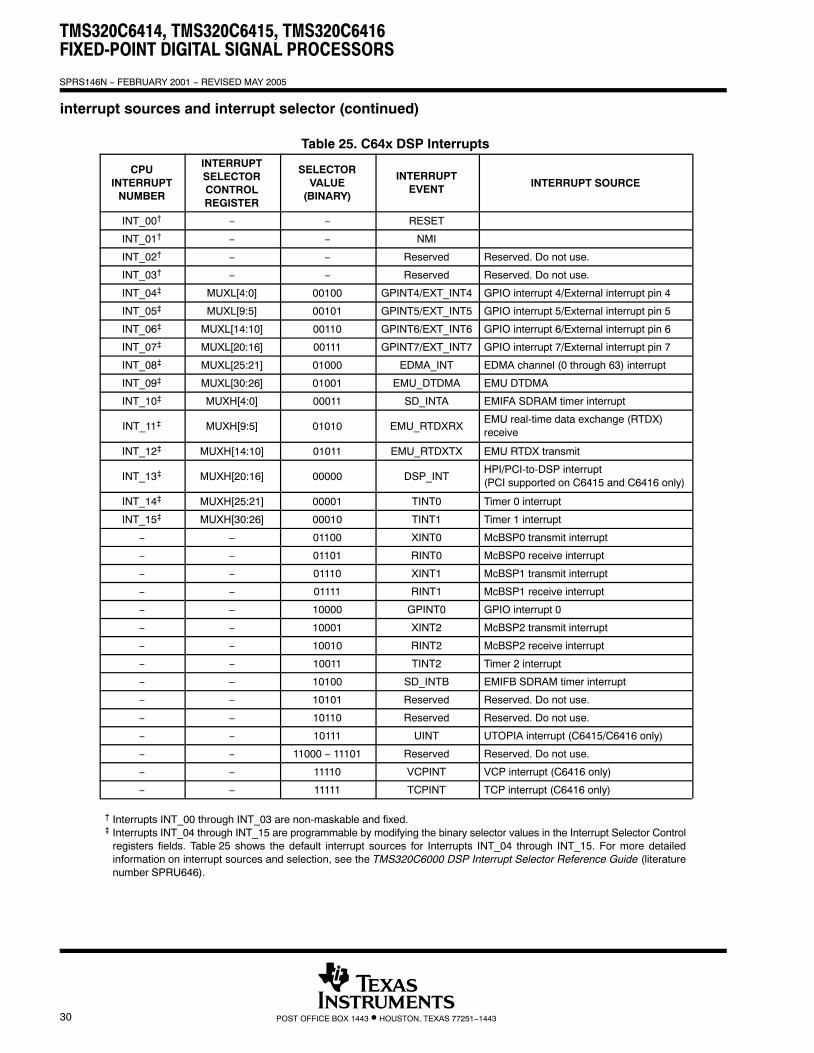
Table 25. C64x DSP Interrupts
CPUINTERRUPT
NUMBER
INTERRUPTSELECTORCONTROLREGISTER
SELECTORVALUE
(BINARY)
INTERRUPTEVENT INTERRUPT SOURCE
INT_00† − − RESET
INT_01† − − NMI
INT_02† − − Reserved Reserved. Do not use.
INT_03† − − Reserved Reserved. Do not use.
INT_04‡ MUXL[4:0] 00100 GPINT4/EXT_INT4 GPIO interrupt 4/External interrupt pin 4
INT_05‡ MUXL[9:5] 00101 GPINT5/EXT_INT5 GPIO interrupt 5/External interrupt pin 5
INT_06‡ MUXL[14:10] 00110 GPINT6/EXT_INT6 GPIO interrupt 6/External interrupt pin 6
INT_07‡ MUXL[20:16] 00111 GPINT7/EXT_INT7 GPIO interrupt 7/External interrupt pin 7
INT_08‡ MUXL[25:21] 01000 EDMA_INT EDMA channel (0 through 63) interrupt
INT_09‡ MUXL[30:26] 01001 EMU_DTDMA EMU DTDMA
INT_10‡ MUXH[4:0] 00011 SD_INTA EMIFA SDRAM timer interrupt
INT_11‡ MUXH[9:5] 01010 EMU_RTDXRXEMU real-time data exchange (RTDX)receive
INT_12‡ MUXH[14:10] 01011 EMU_RTDXTX EMU RTDX transmit
INT_13‡ MUXH[20:16] 00000 DSP_INTHPI/PCI-to-DSP interrupt (PCI supported on C6415 and C6416 only)
INT_14‡ MUXH[25:21] 00001 TINT0 Timer 0 interrupt
INT_15‡ MUXH[30:26] 00010 TINT1 Timer 1 interrupt
− − 01100 XINT0 McBSP0 transmit interrupt
− − 01101 RINT0 McBSP0 receive interrupt
− − 01110 XINT1 McBSP1 transmit interrupt
− − 01111 RINT1 McBSP1 receive interrupt
− − 10000 GPINT0 GPIO interrupt 0
− − 10001 XINT2 McBSP2 transmit interrupt
− − 10010 RINT2 McBSP2 receive interrupt
− − 10011 TINT2 Timer 2 interrupt
− − 10100 SD_INTB EMIFB SDRAM timer interrupt
− − 10101 Reserved Reserved. Do not use.
− − 10110 Reserved Reserved. Do not use.
− − 10111 UINT UTOPIA interrupt (C6415/C6416 only)
− − 11000 − 11101 Reserved Reserved. Do not use.
− − 11110 VCPINT VCP interrupt (C6416 only)
− − 11111 TCPINT TCP interrupt (C6416 only)
† Interrupts INT_00 through INT_03 are non-maskable and fixed.‡ Interrupts INT_04 through INT_15 are programmable by modifying the binary selector values in the Interrupt Selector Control
registers fields. Table 25 shows the default interrupt sources for Interrupts INT_04 through INT_15. For more detailedinformation on interrupt sources and selection, see the TMS320C6000 DSP Interrupt Selector Reference Guide (literaturenumber SPRU646).

TMS320C6414, TMS320C6415, TMS320C6416FIXED-POINT DIGITAL SIGNAL PROCESSORS
SPRS146N − FEBRUARY 2001 − REVISED MAY 2005
31POST OFFICE BOX 1443 • HOUSTON, TEXAS 77251−1443
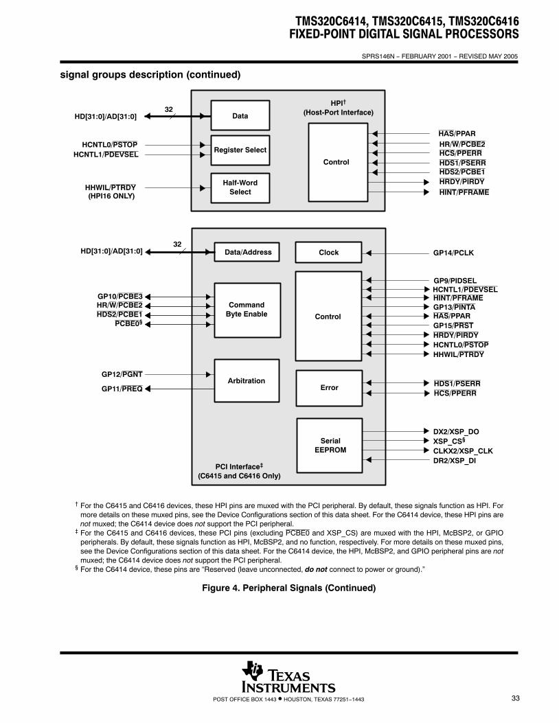
signal groups description
TRST
GP7/EXT_INT7‡
IEEE Standard1149.1(JTAG)
Emulation
Reserved
Reset andInterrupts
Control/Status
TDITDOTMS
TCK
EMU0EMU1
NMI
GP6/EXT_INT6‡
GP5/EXT_INT5‡
GP4/EXT_INT4‡
RESET
RSVRSV
RSVRSV
Clock/PLL
CLKIN
CLKMODE1CLKMODE0
PLLV
EMU2EMU3EMU4EMU5
RSV
GPIO
General-Purpose Input/Output (GPIO) Port
GP7/EXT_INT7‡
GP6/EXT_INT6‡
GP5/EXT_INT5‡
GP4/EXT_INT4‡
GP3CLKOUT6/GP2†
CLKOUT4/GP1†
GP0
CLKOUT6/GP2†CLKOUT4/GP1†
EMU6EMU7EMU8EMU9
EMU10
GP15/PRST§
GP14/PCLK§
GP13/PINTA§
GP12/PGNT§
GP11/PREQ§
GP10/PCBE3§
GP9/PIDSEL§
CLKS2/GP8†
These pins are muxed with the GPIO port pins and by default these signals function as clocks (CLKOUT4 or CLKOUT6) or McBSP2clock source (CLKS2). To use these muxed pins as GPIO signals, the appropriate GPIO register bits (GPxEN and GPxDIR) must beproperly enabled and configured. For more details, see the Device Configurations section of this data sheet.
†
These pins are GPIO pins that can also function as external interrupt sources (EXT_INT[7:4]). Default after reset is EXT_INTx orGPIO as input-only.
‡
RSV
EMU11
RSVRSV
RSV
••
•
PeripheralControl/Status
PCI_ENMCBSP2_EN
For the C6415 and C6416 devices, these GPIO pins are muxed with the PCI peripheral pins. By default, these signals are set up tono function with both the GPIO and PCI pin functions disabled. For more details on these muxed pins, see the Device Configurationssection of this data sheet. For the C6414 device, the GPIO peripheral pins are not muxed; the C6414 device does not support thePCI peripheral.
§
Figure 3. CPU and Peripheral Signals
TMS320C6414, TMS320C6415, TMS320C6416FIXED-POINT DIGITAL SIGNAL PROCESSORS
SPRS146N − FEBRUARY 2001 − REVISED MAY 2005
32 POST OFFICE BOX 1443 • HOUSTON, TEXAS 77251−1443
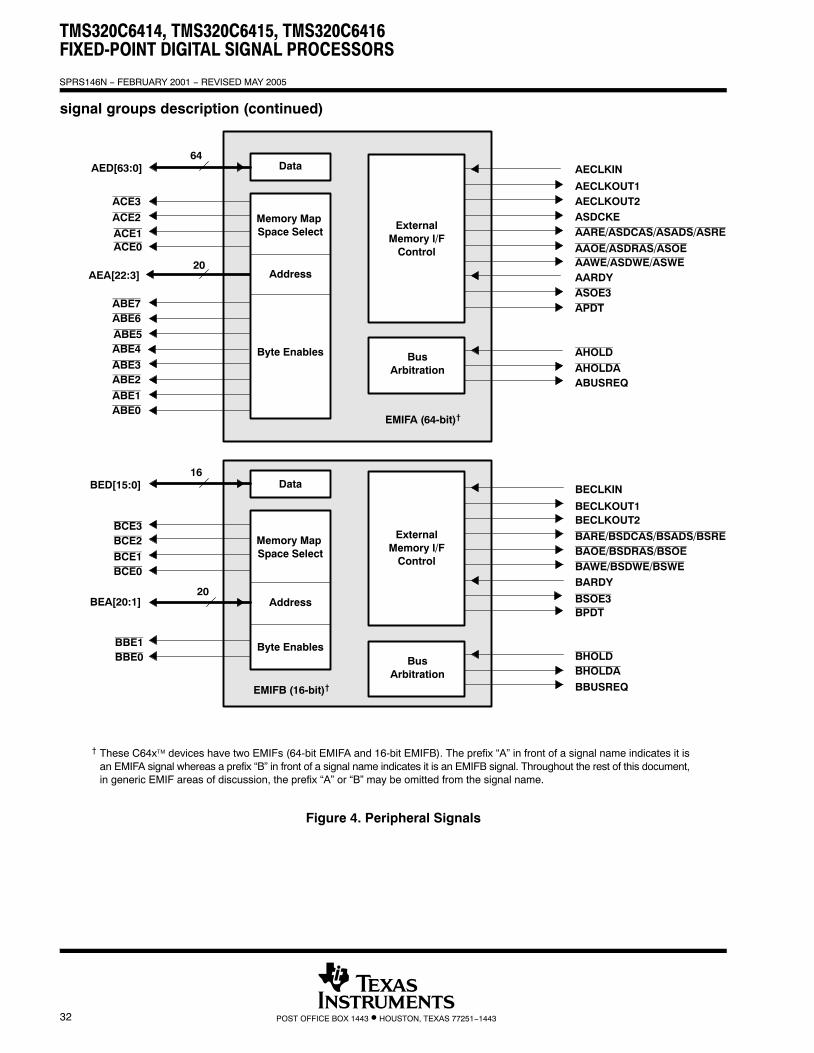
signal groups description (continued)
ACE3AECLKOUT1
AED[63:0]
ACE2
ACE1ACE0
AEA[22:3]
ABE7ABE6
ABE5ABE4
AARDY
Data
Memory Map Space Select
Address
Byte Enables
64
20
ExternalMemory I/F
Control
EMIFA (64-bit)†
AECLKIN
AHOLD
AHOLDAABUSREQ
BusArbitration
AARE/ASDCAS/ASADS/ASREASDCKEAECLKOUT2
ASOE3
ABE3ABE2
ABE1ABE0
BCE3
BED[15:0]
BCE2
BCE1BCE0
BEA[20:1]
Data
Memory Map Space Select
Address
Byte Enables
16
ExternalMemory I/F
Control
BECLKIN
BHOLDBHOLDA
BBUSREQ
BusArbitration
BSOE3
BBE1BBE0
EMIFB (16-bit)†
BECLKOUT1
BARDY
BECLKOUT2
AAOE/ASDRAS/ASOEAAWE/ASDWE/ASWE
BARE/BSDCAS/BSADS/BSREBAOE/BSDRAS/BSOEBAWE/BSDWE/BSWE
BPDT
APDT
† These C64x™ devices have two EMIFs (64-bit EMIFA and 16-bit EMIFB). The prefix “A” in front of a signal name indicates it isan EMIFA signal whereas a prefix “B” in front of a signal name indicates it is an EMIFB signal. Throughout the rest of this document,in generic EMIF areas of discussion, the prefix “A” or “B” may be omitted from the signal name.
20
Figure 4. Peripheral Signals
TMS320C6414, TMS320C6415, TMS320C6416FIXED-POINT DIGITAL SIGNAL PROCESSORS
SPRS146N − FEBRUARY 2001 − REVISED MAY 2005
33POST OFFICE BOX 1443 • HOUSTON, TEXAS 77251−1443
signal groups description (continued)
HHWIL/PTRDY
HCNTL0/PSTOPHCNTL1/PDEVSEL
Data
Register Select
Half-WordSelect
Control
HPI†
(Host-Port Interface)32HD[31:0]/AD[31:0]
HAS/PPARHR/W/PCBE2HCS/PPERRHDS1/PSERRHDS2/PCBE1HRDY/PIRDYHINT/PFRAME(HPI16 ONLY)
† For the C6415 and C6416 devices, these HPI pins are muxed with the PCI peripheral. By default, these signals function as HPI. Formore details on these muxed pins, see the Device Configurations section of this data sheet. For the C6414 device, these HPI pins arenot muxed; the C6414 device does not support the PCI peripheral.
‡ For the C6415 and C6416 devices, these PCI pins (excluding PCBE0 and XSP_CS) are muxed with the HPI, McBSP2, or GPIOperipherals. By default, these signals function as HPI, McBSP2, and no function, respectively. For more details on these muxed pins,see the Device Configurations section of this data sheet. For the C6414 device, the HPI, McBSP2, and GPIO peripheral pins are notmuxed; the C6414 device does not support the PCI peripheral.
§ For the C6414 device, these pins are “Reserved (leave unconnected, do not connect to power or ground).”
HD[31:0]/AD[31:0]
HR/W/PCBE2HDS2/PCBE1
PCBE0§
GP12/PGNT
GP11/PREQ
GP14/PCLK
HINT/PFRAMEGP13/PINTA
Data/Address
Arbitration
32Clock
Control
PCI Interface‡
(C6415 and C6416 Only)
HAS/PPARGP15/PRSTHRDY/PIRDYHCNTL0/PSTOPHHWIL/PTRDY
GP10/PCBE3
GP9/PIDSELHCNTL1/PDEVSEL
HDS1/PSERRError
CommandByte Enable
SerialEEPROM
DX2/XSP_DOXSP_CS§
CLKX2/XSP_CLKDR2/XSP_DI
HCS/PPERR
Figure 4. Peripheral Signals (Continued)

TMS320C6414, TMS320C6415, TMS320C6416FIXED-POINT DIGITAL SIGNAL PROCESSORS
SPRS146N − FEBRUARY 2001 − REVISED MAY 2005
34 POST OFFICE BOX 1443 • HOUSTON, TEXAS 77251−1443
signal groups description (continued)
McBSPs(Multichannel Buffered
Serial Ports)
CLKX0FSX0DX0
CLKR0FSR0
DR0
CLKS0
Transmit
McBSP0
Receive
Clock
CLKX1/URADDR4†
FSX1/UXADDR3†
DX1/UXADDR4†
CLKR1/URADDR2†
FSR1/UXADDR2†
DR1/UXADDR1†
CLKS1/URADDR3†
Transmit
McBSP1
Receive
Clock
CLKX2/XSP_CLK†
FSX2DX2/XSP_DO†
CLKR2FSR2
DR2/XSP_DI†
CLKS2/GP8‡
Transmit
McBSP2
Receive
Clock
† For the C6415 and C6416 devices, these McBSP2 and McBSP1 pins are muxed with the PCI and UTOPIA peripherals, respectively.By default, these signals function as McBSP2 and McBSP1, respectively. For more details on these muxed pins, see the DeviceConfigurations section of this data sheet. For the C6414 device, these McBSP2 and McBSP1 peripheral pins are not muxed; the C6414 device does not support PCI and UTOPIAperipherals.
‡ The McBSP2 clock source pin (CLKS2, default) is muxed with the GP8 pin. To use this muxed pin as the GP8 signal, the appropriateGPIO register bits (GP8EN and GP8DIR) must be properly enabled and configured. For more details, see the Device Configurationssection of this data sheet.
Figure 4. Peripheral Signals (Continued)

TMS320C6414, TMS320C6415, TMS320C6416FIXED-POINT DIGITAL SIGNAL PROCESSORS
SPRS146N − FEBRUARY 2001 − REVISED MAY 2005
35POST OFFICE BOX 1443 • HOUSTON, TEXAS 77251−1443
signal groups description (continued)
CLKR1/URADDR2†Control/Status
CLKX1/URADDR4†
URDATA0URDATA1
CLKS1/URADDR3†
URADDR1URADDR0
Receive
URDATA7
URDATA4URDATA3URDATA2
URCLAV
URENB
URDATA5URDATA6
URSOC
URCLK Clock
Control/Status
Transmit
Clock
FSR1/UXADDR2†
DX1/UXADDR4†
UXDATA0UXDATA1
FSX1/UXADDR3†
DR1/UXADDR1†
UXADDR0
UXDATA7
UXDATA4UXDATA3UXDATA2
UXCLAV
UXENB
UXDATA5UXDATA6
UXSOC
UXCLK
UTOPIA (SLAVE) [C6415 and C6416 Only]
† For the C6415 and C6416 devices, these UTOPIA pins are muxed with the McBSP1 peripheral. By default, these signals function asMcBSP1. For more details on these muxed pins, see the Device Configurations section of this data sheet. For the C6414 device, these McBSP1 peripheral pins are not muxed; the C6414 does not support the UTOPIA peripheral.
TOUT0
Timers
TINP0TOUT1
Timer 1TINP1
TOUT2Timer 2
TINP2
Timer 0
Figure 4. Peripheral Signals (Continued)

TMS320C6414, TMS320C6415, TMS320C6416FIXED-POINT DIGITAL SIGNAL PROCESSORS
SPRS146N − FEBRUARY 2001 − REVISED MAY 2005
36 POST OFFICE BOX 1443 • HOUSTON, TEXAS 77251−1443
DEVICE CONFIGURATIONS
The C6414, C6415, and C6416 peripheral selections and other device configurations are determined byexternal pullup/pulldown resistors on the following pins (all of which are latched during device reset):
peripherals selection (C6415 and C6416 devices)
− BEA11 (UTOPIA_EN)
− PCI_EN (for C6415 or C6416, see Table 27 footnotes)
− MCBSP2_EN (for C6415 or C6416, see Table 27 footnotes)
The C6414 device does not support the PCI and UTOPIA peripherals; for proper operation of the C6414device, do not oppose the internal pulldowns (IPDs) on the BEA11, PCI_EN, and MCBSP2_EN pins. (ForIPUs/IPDs on pins, see the Terminal Functions table of this data sheet.)
other device configurations (C64x)
− BEA[20:13, 7]
− HD5
peripherals selection
Some C6415/C6416 peripherals share the same pins (internally muxed) and are mutually exclusive (i.e., HPI,general-purpose input/output pins GP[15:9], PCI and its internal EEPROM, McBSP1, McBSP2, and UTOPIA).The VCP/TCP coprocessors (C6416 only) and other C64x peripherals (i.e., the Timers, McBSP0, and theGP[8:0] pins), are always available.
UTOPIA and McBSP1 peripherals
The UTOPIA_EN pin (BEA11) is latched at reset. For C6415 and C6416 devices, this pin selects whetherthe UTOPIA peripheral or McBSP1 peripheral is functionally enabled (see Table 26).
The C6414 device does not support the UTOPIA peripheral; for proper device operation, do not oppose theinternal pulldown (IPD) on the BEA11 pin.
Table 26. UTOPIA_EN Peripheral Selection (McBSP1 and UTOPIA) (C6415/C6416 Only)
PERIPHERAL SELECTION PERIPHERALS SELECTED
UTOPIA_EN (BEA11) Pin [D16] UTOPIA McBSP1
DESCRIPTION
0 √McBSP1 is enabled and UTOPIA is disabled [default]. This means all multiplexed McBSP1/UTOPIA pins function as McBSP1and all other standalone UTOPIA pins are tied-off (Hi-Z).
1 √UTOPIA is enabled and McBSP1 is disabled. This means all multiplexed McBSP1/UTOPIA pins now function asUTOPIA and all other standalone McBSP1 pins are tied-off (Hi-Z).
HPI, GP[15:9], PCI, EEPROM (internal to PCI), and McBSP2 peripherals
The PCI_EN and MCBSP2_EN pins are latched at reset. They determine specific peripheral selection forthe C6415 and C6416 devices, summarized in Table 27.
The C6414 device does not support the PCI peripheral; for proper device operation, do not oppose theinternal pulldowns (IPDs) on the PCI_EN and MCBSP2_EN pins.
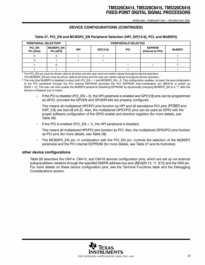
TMS320C6414, TMS320C6415, TMS320C6416FIXED-POINT DIGITAL SIGNAL PROCESSORS
SPRS146N − FEBRUARY 2001 − REVISED MAY 2005
37POST OFFICE BOX 1443 • HOUSTON, TEXAS 77251−1443
DEVICE CONFIGURATIONS (CONTINUED)
Table 27. PCI_EN and MCBSP2_EN Peripheral Selection (HPI, GP[15:9], PCI, and McBSP2)
PERIPHERAL SELECTION† PERIPHERALS SELECTED
PCI_ENPin [AA4]
MCBSP2_ENPin [AF3] HPI GP[15:9] PCI
EEPROM(Internal to PCI) McBSP2
0 0 √ √ √
0 1 √ √ √
1 0 √ √ ‡
1 1 à à The PCI_EN pin must be driven valid at all times and the user must not switch values throughout device operation.
The MCBSP2_EN pin must be driven valid at all times and the user can switch values throughout device operation.‡ The only time McBSP2 is disabled is when both PCI_EN = 1 and MCBSP2_EN = 0. This configuration enables, at reset, the auto-initialization
of the PCI peripheral through the PCI internal EEPROM [provided the PCI EEPROM Auto-Initialization pin (BEA13) is pulled up(EEAI = 1)]. The user can then enable the McBSP2 peripheral (disabling EEPROM) by dynamically changing MCBSP2_EN to a “1” after thedevice is initialized (out of reset).
− If the PCI is disabled (PCI_EN = 0), the HPI peripheral is enabled and GP[15:9] pins can be programmedas GPIO, provided the GPxEN and GPxDIR bits are properly configured.
This means all multiplexed HPI/PCI pins function as HPI and all standalone PCI pins (PCBE0 and XSP_CS) are tied-off (Hi-Z). Also, the multiplexed GPIO/PCI pins can be used as GPIO with the proper software configuration of the GPIO enable and direction registers (for more details, see Table 29).
− If the PCI is enabled (PCI_EN = 1), the HPI peripheral is disabled.
This means all multiplexed HPI/PCI pins function as PCI. Also, the multiplexed GPIO/PCI pins functionas PCI pins (for more details, see Table 29).
− The MCBSP2_EN pin, in combination with the PCI_EN pin, controls the selection of the McBSP2peripheral and the PCI internal EEPROM (for more details, see Table 27 and its footnotes).
other device configurations
Table 28 describes the C6414, C6415, and C6416 devices configuration pins, which are set up via externalpullup/pulldown resistors through the specified EMIFB address bus pins (BEA[20:13, 11, 9:7]) and the HD5 pin.For more details on these device configuration pins, see the Terminal Functions table and the DebuggingConsiderations section.
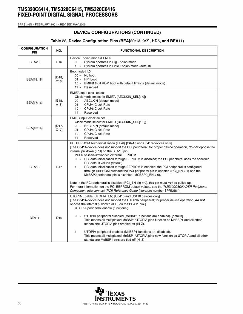
TMS320C6414, TMS320C6415, TMS320C6416FIXED-POINT DIGITAL SIGNAL PROCESSORS
SPRS146N − FEBRUARY 2001 − REVISED MAY 2005
38 POST OFFICE BOX 1443 • HOUSTON, TEXAS 77251−1443
DEVICE CONFIGURATIONS (CONTINUED)
Table 28. Device Configuration Pins (BEA[20:13, 9:7], HD5, and BEA11)
CONFIGURATIONPIN NO. FUNCTIONAL DESCRIPTION
BEA20 E16Device Endian mode (LEND)
0 – System operates in Big Endian mode1 − System operates in Little Endian mode (default)
BEA[19:18][D18,C18]
Bootmode [1:0]00 – No boot01 − HPI boot10 − EMIFB 8-bit ROM boot with default timings (default mode)11 − Reserved
BEA[17:16][B18,A18]
EMIFA input clock select Clock mode select for EMIFA (AECLKIN_SEL[1:0])00 – AECLKIN (default mode)01 − CPU/4 Clock Rate10 − CPU/6 Clock Rate11 − Reserved
BEA[15:14][D17,C17]
EMIFB input clock select Clock mode select for EMIFB (BECLKIN_SEL[1:0])00 – BECLKIN (default mode)01 − CPU/4 Clock Rate10 − CPU/6 Clock Rate11 − Reserved
BEA13 B17
PCI EEPROM Auto-Initialization (EEAI) [C6415 and C6416 devices only][The C6414 device does not support the PCI peripheral; for proper device operation, do not oppose theinternal pulldown (IPD) on the BEA13 pin.]
PCI auto-initialization via external EEPROM0 − PCI auto-initialization through EEPROM is disabled; the PCI peripheral uses the specified
PCI default values (default). 1 − PCI auto-initialization through EEPROM is enabled; the PCI peripheral is configured
through EEPROM provided the PCI peripheral pin is enabled (PCI_EN = 1) and the McBSP2 peripheral pin is disabled (MCBSP2_EN = 0).
Note: If the PCI peripheral is disabled (PCI_EN pin = 0), this pin must not be pulled up.For more information on the PCI EEPROM default values, see the TMS320C6000 DSP PeripheralComponent Interconnect (PCI) Reference Guide (literature number SPRU581).
BEA11 D16
UTOPIA Enable (UTOPIA_EN) [C6415 and C6416 devices only][The C6414 device does not support the UTOPIA peripheral; for proper device operation, do notoppose the internal pulldown (IPD) on the BEA11 pin.]
UTOPIA peripheral enable (functional)
0 − UTOPIA peripheral disabled (McBSP1 functions are enabled). [default]This means all multiplexed McBSP1/UTOPIA pins function as McBSP1 and all other standalone UTOPIA pins are tied-off (Hi-Z).
1 − UTOPIA peripheral enabled (McBSP1 functions are disabled).This means all multiplexed McBSP1/UTOPIA pins now function as UTOPIA and all other standalone McBSP1 pins are tied-off (Hi-Z).

TMS320C6414, TMS320C6415, TMS320C6416FIXED-POINT DIGITAL SIGNAL PROCESSORS
SPRS146N − FEBRUARY 2001 − REVISED MAY 2005
39POST OFFICE BOX 1443 • HOUSTON, TEXAS 77251−1443
DEVICE CONFIGURATIONS (CONTINUED)
Table 28. Device Configuration Pins (BEA[20:13, 9:7], HD5, and BEA11) (Continued)
CONFIGURATIONPIN NO. FUNCTIONAL DESCRIPTION
BEA7BEA8BEA9
D15A16B16
C6414 Devices C6415 Devices C6416 Devices
Do not oppose internal pulldown (IPD) Pullup† Do not oppose IPDDo not oppose IPD Do not oppose IPD Pullup†
Do not oppose IPD Do not oppose IPD Pullup†
†For proper device operation, this pin must be externally pulled up with a 1-kΩ resistor.
HD5 Y1
HPI peripheral bus width (HPI_WIDTH)0 − HPI operates as an HPI16.
(HPI bus is 16 bits wide. HD[15:0] pins are used and the remaining HD[31:16] pins are reserved pins in the Hi-Z state.)
1 − HPI operates as an HPI32.(HPI bus is 32 bits wide. All HD[31:0] pins are used for host-port operations.)
TMS320C6414, TMS320C6415, TMS320C6416FIXED-POINT DIGITAL SIGNAL PROCESSORS
SPRS146N − FEBRUARY 2001 − REVISED MAY 2005
40 POST OFFICE BOX 1443 • HOUSTON, TEXAS 77251−1443
DEVICE CONFIGURATIONS (CONTINUED)
multiplexed pins
Multiplexed pins are pins that are shared by more than one peripheral and are internally multiplexed. Some ofthese pins are configured by software, and the others are configured by external pullup/pulldown resistors onlyat reset. Those muxed pins that are configured by software can be programmed to switch functionalities at anytime. Those muxed pins that are configured by external pullup/pulldown resistors are mutually exclusive; onlyone peripheral has primary control of the function of these pins after reset. Table 29 identifies the multiplexedpins on the C6414, C6415, and C6416 devices; shows the default (primary) function and the default settingsafter reset; and describes the pins, registers, etc. necessary to configure specific multiplexed functions.
debugging considerations
It is recommended that external connections be provided to device configuration pins, includingCLKMODE[1:0], BEA[20:13, 11, 9:7], HD5/AD5, PCI_EN, and MCBSP2_EN. Although internal pullup/pulldownresistors exist on these pins (except for HD5/AD5), providing external connectivity adds convenience to the userin debugging and flexibility in switching operating modes.
Internal pullup/pulldown resistors also exist on the non-configuration pins on the BEA bus (BEA[12, 10, 6:1]).Do not oppose the internal pullup/pulldown resistors on these non-configuration pins with externalpullup/pulldown resistors. If an external controller provides signals to these non-configuration pins, thesesignals must be driven to the default state of the pins at reset, or not be driven at all.
For the internal pullup/pulldown resistors on the C6414, C6415, and C6416 device pins, see the terminalfunctions table.

TMS320C6414, TMS320C6415, TMS320C6416FIXED-POINT DIGITAL SIGNAL PROCESSORS
SPRS146N − FEBRUARY 2001 − REVISED MAY 2005
41POST OFFICE BOX 1443 • HOUSTON, TEXAS 77251−1443
DEVICE CONFIGURATIONS (CONTINUED)
Table 29. C6414, C6415, and C6416 Device Multiplexed Pins†
MULTIPLEXED PINSDEFAULT FUNCTION DEFAULT SETTING DESCRIPTION
NAME NO.DEFAULT FUNCTION DEFAULT SETTING DESCRIPTION
CLKOUT4/GP1‡ AE6 CLKOUT4 GP1EN = 0 (disabled)These pins are software-configurable.To use these pins as GPIO pins, theGPxEN bits in the GPIO Enable
CLKOUT6/GP2‡ AD6 CLKOUT6 GP2EN = 0 (disabled)
GPxEN bits in the GPIO EnableRegister and the GPxDIR bits in theGPIO Direction Register must beproperly configured.
CLKS2/GP8‡ AE4 CLKS2 GP8EN = 0 (disabled)
properly configured.GPxEN = 1: GPx pin enabledGPxDIR = 0: GPx pin is an inputGPxDIR = 1: GPx pin is an output
GP9/PIDSEL M3 To use GP[15:9] as GPIO pins, the PCI
GP10/PCBE3 L2
To use GP[15:9] as GPIO pins, the PCIneeds to be disabled (PCI_EN = 0), theGPxEN bits in the GPIO Enable
GP11/PREQ F1GP EN 0 (di bl d)
GPxEN bits in the GPIO EnableRegister and the GPxDIR bits in the
GP12/PGNT J3 NoneGPxEN = 0 (disabled)PCI EN = 0 (disabled)†
Register and the GPxDIR bits in theGPIO Direction Register must be
GP13/PINTA G4
None PCI_EN = 0 (disabled)†GPIO Direction Register must beproperly configured.
GPxEN 1: GPx pin enabledGP14/PCLK F2
GPxEN = 1: GPx pin enabledGPxDIR = 0: GPx pin is an input
GP15/PRST G3GPxDIR = 0: GPx pin is an inputGPxDIR = 1: GPx pin is an output
DX1/UXADDR4 AB11 DX1
FSX1/UXADDR3 AB13 FSX1 By default, McBSP1 is enabled uponFSR1/UXADDR2 AC9 FSR1
UTOPIA EN (BEA11) 0
By default, McBSP1 is enabled uponreset (UTOPIA is disabled).T bl h UTOPIA i h l DR1/UXADDR1 AF11 DR1
UTOPIA_EN (BEA11) = 0(disabled)†
( )To enable the UTOPIA peripheral, anexternal pullup resistor (1 kΩ) must be
CLKX1/URADDR4 AB12 CLKX1(disabled)† external pullup resistor (1 kΩ) must be
provided on the BEA11 pin (settingCLKS1/URADDR3 AC8 CLKS1
provided on the BEA11 pin (settingUTOPIA_EN = 1 at reset).
CLKR1/URADDR2 AC10 CLKR1
_ )
CLKX2/XSP_CLK AC2 CLKX2
DR2/XSP_DI AB3 DR2
DX2/XSP_DO AA2 DX2
HD[31:0]/AD[31:0] § HD[31:0]
HAS/PPAR T3 HAS
HCNTL1/PDEVSEL R1 HCNTL1 By default, HPI is enabled upon reset(PCI is disabled)
HCNTL0/PSTOP T4 HCNTL0PCI EN 0 (disabled)†
(PCI is disabled). To enable the PCI peripheral an external
HDS1/PSERR T1 HDS1PCI_EN = 0 (disabled)†
To enable the PCI peripheral an externalpullup resistor (1 kΩ) must be provided
h PCI EN i ( i PCI EN 1HDS2/PCBE1 T2 HDS2
p p ( ) pon the PCI_EN pin (setting PCI_EN = 1at reset)
HR/W/PCBE2 P1 HR/Wat reset).
HHWIL/PTRDY R3 HHWIL (HPI16 only)
HINT/PFRAME R4 HINT
HCS/PPERR R2 HCS
HRDY/PIRDY P4 HRDY† For the C6415 and C6416 devices, all other standalone UTOPIA and PCI pins are tied-off internally (pins in Hi-Z) when the peripheral is disabled
[UTOPIA_EN (BEA11) = 0 or PCI_EN = 0].‡ The C6414 device does not support the PCI and UTOPIA peripherals. These are the only multiplexed pins on the C6414 device, all other pins
are standalone peripheral functions and are not muxed.§ For the HD[31:0]/AD[31:0] multiplexed pins pin numbers, see the Terminal Functions table.

TMS320C6414, TMS320C6415, TMS320C6416FIXED-POINT DIGITAL SIGNAL PROCESSORS
SPRS146N − FEBRUARY 2001 − REVISED MAY 2005
42 POST OFFICE BOX 1443 • HOUSTON, TEXAS 77251−1443
Terminal Functions SIGNAL
TYPE† IPD/DESCRIPTION
NAME NO. TYPE† IPD/IPU‡ DESCRIPTION
CLOCK/PLL CONFIGURATION
CLKIN H4 I IPD Clock Input. This clock is the input to the on-chip PLL.
CLKOUT4/GP1§ AE6 I/O/Z IPDClock output at 1/4 of the device speed (O/Z) [default] or this pin can be programmed as aGPIO 1 pin (I/O/Z).
CLKOUT6/GP2§ AD6 I/O/Z IPDClock output at 1/6 of the device speed (O/Z) [default] or this pin can be programmed as aGPIO 2 pin (I/O/Z).
CLKMODE1 G1 I IPD Clock mode select• Selects whether the CPU clock frequency = input clock frequency x1 (Bypass), x6, or x12.
CLKMODE0 H2 I IPD
• Selects whether the CPU clock frequency = input clock frequency x1 (Bypass), x6, or x12.For more details on the CLKMODE pins and the PLL multiply factors, see the Clock PLLsection of this data sheet.
PLLV¶ J6 A# PLL voltage supply
JTAG EMULATION
TMS AB16 I IPU JTAG test-port mode select
TDO AE19 O/Z IPU JTAG test-port data out
TDI AF18 I IPU JTAG test-port data in
TCK AF16 I IPU JTAG test-port clock
TRST AB15 I IPDJTAG test-port reset. For IEEE 1149.1 JTAG compatibility, see the IEEE 1149.1 JTAG Compatibility Statement section of this data sheet.
EMU11 AC18 I/O/Z IPU Emulation pin 11. Reserved for future use, leave unconnected.
EMU10 AD18 I/O/Z IPU Emulation pin 10. Reserved for future use, leave unconnected.
EMU9 AE18 I/O/Z IPU Emulation pin 9. Reserved for future use, leave unconnected.
EMU8 AC17 I/O/Z IPU Emulation pin 8. Reserved for future use, leave unconnected.
EMU7 AF17 I/O/Z IPU Emulation pin 7. Reserved for future use, leave unconnected.
EMU6 AD17 I/O/Z IPU Emulation pin 6. Reserved for future use, leave unconnected.
EMU5 AE17 I/O/Z IPU Emulation pin 5. Reserved for future use, leave unconnected.
EMU4 AC16 I/O/Z IPU Emulation pin 4. Reserved for future use, leave unconnected.
EMU3 AD16 I/O/Z IPU Emulation pin 3. Reserved for future use, leave unconnected.
EMU2 AE16 I/O/Z IPU Emulation pin 2. Reserved for future use, leave unconnected.
EMU1EMU0
AC15AF15
I/O/Z IPU
Emulation [1:0] pins• Select the device functional mode of operation
EMU[1:0] Operation00 Boundary Scan/Normal Mode (see Note)01 Reserved10 Reserved11 Emulation/Normal Mode [default] (see the IEEE 1149.1 JTAG
Compatibility Statement section of this data sheet)Normal mode refers to the DSPs normal operational mode, when the DSP is free running. TheDSP can be placed in normal operational mode when the EMU[1:0] pins are configured foreither Boundary Scan or Emulation.
Note: When the EMU[1:0] pins are configured for Boundary Scan mode, the internal pulldown(IPD) on the TRST signal must not be opposed in order to operate in Normal mode.For the Boundary Scan mode pulldown EMU[1:0] pins with a dedicated 1-kΩ resister.
† I = Input, O = Output, Z = High impedance, S = Supply voltage, GND = Ground‡ IPD = Internal pulldown, IPU = Internal pullup. (These IPD/IPU signal pins feature a 30-kΩ IPD or IPU resistor. To pull up a signal to the opposite
supply rail, a 1-kΩ resistor should be used.)§ These pins are multiplexed pins. For more details, see the Device Configurations section of this data sheet.¶ PLLV is not part of external voltage supply. See the Clock PLL section for information on how to connect this pin.# A = Analog signal (PLL Filter)

TMS320C6414, TMS320C6415, TMS320C6416FIXED-POINT DIGITAL SIGNAL PROCESSORS
SPRS146N − FEBRUARY 2001 − REVISED MAY 2005
43POST OFFICE BOX 1443 • HOUSTON, TEXAS 77251−1443
Terminal Functions (Continued)SIGNAL
TYPE† IPD/DESCRIPTION
NAME NO.TYPE† IPD/
IPU‡ DESCRIPTION
RESETS, INTERRUPTS, AND GENERAL-PURPOSE INPUT/OUTPUTS
RESET AC7 I Device reset
NMI B4 I IPD Nonmaskable interrupt, edge-driven (rising edge)
GP7/EXT_INT7 AF4 General-purpose input/output (GPIO) pins (I/O/Z) or external interrupts (input only). The
GP6/EXT_INT6 AD5I/O/Z IPU
General purpose input/output (GPIO) pins (I/O/Z) or external interrupts (input only). The default after reset setting is GPIO enabled as input-only.• When these pins function as External Interrupts [by selecting the corresponding interrupt
GP5/EXT_INT5 AE5I/O/Z IPU • When these pins function as External Interrupts [by selecting the corresponding interrupt
enable register bit (IER.[7:4])], they are edge-driven and the polarity can be GP4/EXT_INT4 AF5
enable register bit (IER.[7:4])], they are edge-driven and the polarity can be independently selected via the External Interrupt Polarity Register bits (EXTPOL.[3:0]).
GP15/PRST§ G3 General-purpose input/output (GPIO) 15 pin (I/O/Z) or PCI reset (I). No function at default.
GP14/PCLK§ F2 GPIO 14 pin (I/O/Z) or PCI clock (I). No function at default.
GP13/PINTA§ G4 GPIO 13 pin (I/O/Z) or PCI interrupt A (O/Z). No function at default.
GP12/PGNT§ J3 GPIO 12 pin (I/O/Z) or PCI bus grant (I). No function at default.
GP11/PREQ§ F1 GPIO 11 pin (I/O/Z) or PCI bus request (O/Z). No function at default.
GP10/PCBE3§ L2 I/O/Z GPIO 10 pin (I/O/Z) or PCI command/byte enable 3 (I/O/Z). No function at default.
GP9/PIDSEL§ M3
I/O/Z
GPIO 9 pin (I/O/Z) or PCI initialization device select (I). No function at default.
GP3 AC6 IPD GPIO 3 pin (I/O/Z). The default after reset setting is GPIO 3 enabled as input-only.
GP0 AF6 IPD
GPIO 0 pin.The general-purpose I/O 0 pin (GPIO 0) (I/O/Z) can be programmed as GPIO 0 (input only)[default] or as GPIO 0 (output only) pin or output as a general-purpose interrupt (GP0INT)signal (output only).
CLKS2/GP8§¶ AE4 I/O/Z IPDMcBSP2 external clock source (CLKS2) [input only] [default] or this pin can be pro-grammed as a GPIO 8 pin (I/O/Z).
CLKOUT6/GP2§¶ AD6 I/O/Z IPDClock output at 1/6 of the device speed (O/Z) [default] or this pin can be programmed as aGPIO 2 pin (I/O/Z).
CLKOUT4/GP1§¶ AE6 I/O/Z IPDClock output at 1/4 of the device speed (O/Z) [default] or this pin can be programmed as aGPIO 1 pin (I/O/Z).
HOST-PORT INTERFACE (HPI) [C64x] or PERIPHERAL COMPONENT INTERCONNECT (PCI) [C6415 or C6416 devices only]
PCI_EN AA4 I IPD
PCI enable pin. This pin controls the selection (enable/disable) of the HPI and GP[15:9], orPCI peripherals (for the C6415 and C6416 devices). This pin works in conjunction with theMCBSP2_EN pin to enable/disable other peripherals (for more details, see the Device Con-figurations section of this data sheet).
The C6414 device does not support the PCI peripheral; for proper device operation, do notoppose the internal pulldown (IPD) on this pin.
HINT/PFRAME§ R4 I/O/Z Host interrupt from DSP to host (O) [default] or PCI frame (I/O/Z)
HCNTL1/PDEVSEL§ R1 I/O/Z
Host control − selects between control, address, or data registers (I) [default] or PCI device select (I/O/Z).
HCNTL0/PSTOP§ T4 I/O/Z
Host control − selects between control, address, or data registers (I) [default] or PCI stop (I/O/Z)
HHWIL/PTRDY§ R3 I/O/ZHost half-word select − first or second half-word (not necessarily high or low order)[For HPI16 bus width selection only] (I) [default] or PCI target ready (I/O/Z)
HR/W/PCBE2§ P1 I/O/Z Host read or write select (I) [default] or PCI command/byte enable 2 (I/O/Z)† I = Input, O = Output, Z = High impedance, S = Supply voltage, GND = Ground‡ IPD = Internal pulldown, IPU = Internal pullup. (These IPD/IPU signal pins feature a 30-kΩ IPD or IPU resistor. To pull up a signal to the opposite
supply rail, a 1-kΩ resistor should be used.)§ For the C6415 and C6416 devices, these pins are multiplexed pins. For more details, see the Device Configurations section of this data sheet.
The C6414 device does not support the PCI or UTOPIA peripherals; therefore, these muxed peripheral pins are standalone peripheral functionsfor this device.
¶ For the C6414 device, only these pins are multiplexed pins.

TMS320C6414, TMS320C6415, TMS320C6416FIXED-POINT DIGITAL SIGNAL PROCESSORS
SPRS146N − FEBRUARY 2001 − REVISED MAY 2005
44 POST OFFICE BOX 1443 • HOUSTON, TEXAS 77251−1443
Terminal Functions (Continued)SIGNAL
TYPE† IPD/DESCRIPTION
NAME NO.TYPE† IPD/
IPU‡ DESCRIPTION
HOST-PORT INTERFACE (HPI) [C64x] or PERIPHERAL COMPONENT INTERCONNECT (PCI) [C6415 or C6416 devices only] (CONTINUED)
HAS/PPAR§ T3 I/O/Z Host address strobe (I) [default] or PCI parity (I/O/Z)
HCS/PPERR§ R2 I/O/Z Host chip select (I) [default] or PCI parity error (I/O/Z)
HDS1/PSERR§ T1 I/O/Z Host data strobe 1 (I) [default] or PCI system error (I/O/Z)
HDS2/PCBE1§ T2 I/O/Z Host data strobe 2 (I) [default] or PCI command/byte enable 1 (I/O/Z)
HRDY/PIRDY§ P4 I/O/Z Host ready from DSP to host (O) [default] or PCI initiator ready (I/O/Z).
HD31/AD31§ J2
HD30/AD30§ K3
HD29/AD29§ J1
HD28/AD28§ K4
HD27/AD27§ K2
HD26/AD26§ L3
HD25/AD25§ K1
HD24/AD24§ L4
HD23/AD23§ L1
HD22/AD22§ M4 Host-port data (I/O/Z) [default] (C64x) or PCI data-address bus (I/O/Z) [C6415 and C6416]
HD21/AD21§ M2 As HPI data bus (PCI EN pin = 0)HD20/AD20§ N4
As HPI data bus (PCI_EN pin = 0)• Used for transfer of data, address, and control
HD19/AD19§ M1
Used for transfer of data, address, and control• Host-Port bus width user-configurable at device reset via a 10-kΩ resistor pullup/pulldown
resistor on the HD5 pin:HD18/AD18§ N5
resistor on the HD5 pin:
HD17/AD17§ N1 HD5 pin = 0: HPI operates as an HPI16.
HD16/AD16§ P5I/O/Z
HD5 pin 0: HPI operates as an HPI16.(HPI bus is 16 bits wide. HD[15:0] pins are used and the remaining HD[31:16] pins are reserved pins in the high impedance state )
HD15/AD15§ U4I/O/Z reserved pins in the high-impedance state.)
HD14/AD14§ U1 HD5 pin = 1: HPI operates as an HPI32.
HD13/AD13§ U3
5 p ope a es as a 3(HPI bus is 32 bits wide. All HD[31:0] pins are used for host-port operations.)
HD12/AD12§ U2 As PCI data-address bus (PCI EN pin = 1) [C6415 and C6416 devices only]HD11/AD11§ V4
As PCI data-address bus (PCI_EN pin = 1) [C6415 and C6416 devices only]• Used for transfer of data and address
HD10/AD10§ V1The C6414 device does not support the PCI peripheral; therefore the HPI peripheral pins are
HD9/AD9§ V3The C6414 device does not support the PCI peripheral; therefore, the HPI peripheral pins arestandalone peripheral functions, not muxed.
HD8/AD8§ V2standalone peripheral functions, not muxed.
HD7/AD7§ W2
HD6/AD6§ W4
HD5/AD5§ Y1
HD4/AD4§ Y3
HD3/AD3§ Y2
HD2/AD2§ Y4
HD1/AD1§ AA1
HD0/AD0§ AA3† I = Input, O = Output, Z = High impedance, S = Supply voltage, GND = Ground‡ IPD = Internal pulldown, IPU = Internal pullup. (These IPD/IPU signal pins feature a 30-kΩ IPD or IPU resistor. To pull up a signal to the opposite
supply rail, a 1-kΩ resistor should be used.)§ For the C6415 and C6416 devices, these pins are multiplexed pins. For more details, see the Device Configurations section of this data sheet.
The C6414 device does not support the PCI or UTOPIA peripherals; therefore, these muxed peripheral pins are standalone peripheral functionsfor this device.
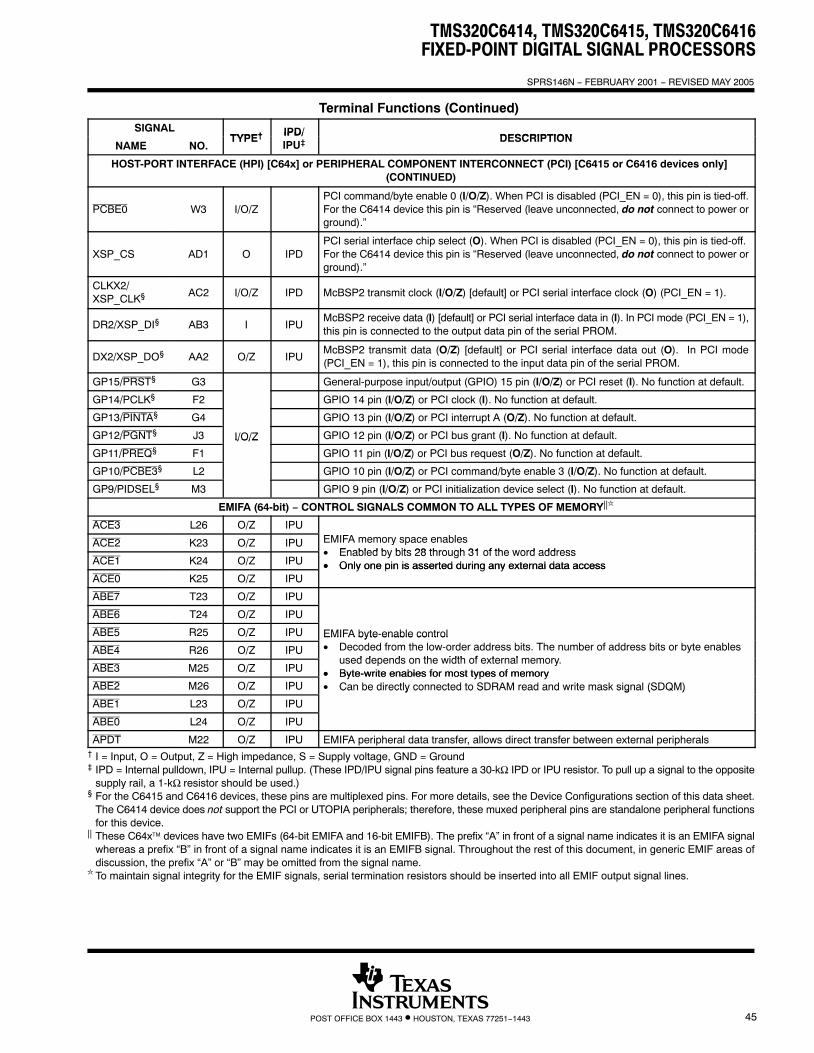
TMS320C6414, TMS320C6415, TMS320C6416FIXED-POINT DIGITAL SIGNAL PROCESSORS
SPRS146N − FEBRUARY 2001 − REVISED MAY 2005
45POST OFFICE BOX 1443 • HOUSTON, TEXAS 77251−1443
Terminal Functions (Continued) SIGNAL
TYPE† IPD/DESCRIPTION
NAME NO.TYPE† IPD/
IPU‡ DESCRIPTION
HOST-PORT INTERFACE (HPI) [C64x] or PERIPHERAL COMPONENT INTERCONNECT (PCI) [C6415 or C6416 devices only] (CONTINUED)
PCBE0 W3 I/O/ZPCI command/byte enable 0 (I/O/Z). When PCI is disabled (PCI_EN = 0), this pin is tied-off.For the C6414 device this pin is “Reserved (leave unconnected, do not connect to power orground).”
XSP_CS AD1 O IPDPCI serial interface chip select (O). When PCI is disabled (PCI_EN = 0), this pin is tied-off.For the C6414 device this pin is “Reserved (leave unconnected, do not connect to power orground).”
CLKX2/XSP_CLK§ AC2 I/O/Z IPD McBSP2 transmit clock (I/O/Z) [default] or PCI serial interface clock (O) (PCI_EN = 1).
DR2/XSP_DI§ AB3 I IPUMcBSP2 receive data (I) [default] or PCI serial interface data in (I). In PCI mode (PCI_EN = 1),this pin is connected to the output data pin of the serial PROM.
DX2/XSP_DO§ AA2 O/Z IPUMcBSP2 transmit data (O/Z) [default] or PCI serial interface data out (O). In PCI mode(PCI_EN = 1), this pin is connected to the input data pin of the serial PROM.
GP15/PRST§ G3 General-purpose input/output (GPIO) 15 pin (I/O/Z) or PCI reset (I). No function at default.
GP14/PCLK§ F2 GPIO 14 pin (I/O/Z) or PCI clock (I). No function at default.
GP13/PINTA§ G4 GPIO 13 pin (I/O/Z) or PCI interrupt A (O/Z). No function at default.
GP12/PGNT§ J3 I/O/Z GPIO 12 pin (I/O/Z) or PCI bus grant (I). No function at default.
GP11/PREQ§ F1
I/O/Z
GPIO 11 pin (I/O/Z) or PCI bus request (O/Z). No function at default.
GP10/PCBE3§ L2 GPIO 10 pin (I/O/Z) or PCI command/byte enable 3 (I/O/Z). No function at default.
GP9/PIDSEL§ M3 GPIO 9 pin (I/O/Z) or PCI initialization device select (I). No function at default.
EMIFA (64-bit) − CONTROL SIGNALS COMMON TO ALL TYPES OF MEMORY||
ACE3 L26 O/Z IPU
ACE2 K23 O/Z IPU EMIFA memory space enables• Enabled by bits 28 through 31 of the word address
ACE1 K24 O/Z IPU• Enabled by bits 28 through 31 of the word address• Only one pin is asserted during any external data access
ACE0 K25 O/Z IPU• Only one pin is asserted during any external data access
ABE7 T23 O/Z IPU
ABE6 T24 O/Z IPU
ABE5 R25 O/Z IPU EMIFA byte-enable control
ABE4 R26 O/Z IPU
EMIFA byte enable control• Decoded from the low-order address bits. The number of address bits or byte enables
used depends on the width of external memoryABE3 M25 O/Z IPU
used depends on the width of external memory.• Byte-write enables for most types of memory
ABE2 M26 O/Z IPU• Byte-write enables for most types of memory• Can be directly connected to SDRAM read and write mask signal (SDQM)
ABE1 L23 O/Z IPU
Can be directly connected to SDRAM read and write mask signal (SDQM)
ABE0 L24 O/Z IPU
APDT M22 O/Z IPU EMIFA peripheral data transfer, allows direct transfer between external peripherals† I = Input, O = Output, Z = High impedance, S = Supply voltage, GND = Ground‡ IPD = Internal pulldown, IPU = Internal pullup. (These IPD/IPU signal pins feature a 30-kΩ IPD or IPU resistor. To pull up a signal to the opposite
supply rail, a 1-kΩ resistor should be used.)§ For the C6415 and C6416 devices, these pins are multiplexed pins. For more details, see the Device Configurations section of this data sheet.
The C6414 device does not support the PCI or UTOPIA peripherals; therefore, these muxed peripheral pins are standalone peripheral functionsfor this device.
|| These C64x™ devices have two EMIFs (64-bit EMIFA and 16-bit EMIFB). The prefix “A” in front of a signal name indicates it is an EMIFA signalwhereas a prefix “B” in front of a signal name indicates it is an EMIFB signal. Throughout the rest of this document, in generic EMIF areas ofdiscussion, the prefix “A” or “B” may be omitted from the signal name.
To maintain signal integrity for the EMIF signals, serial termination resistors should be inserted into all EMIF output signal lines.
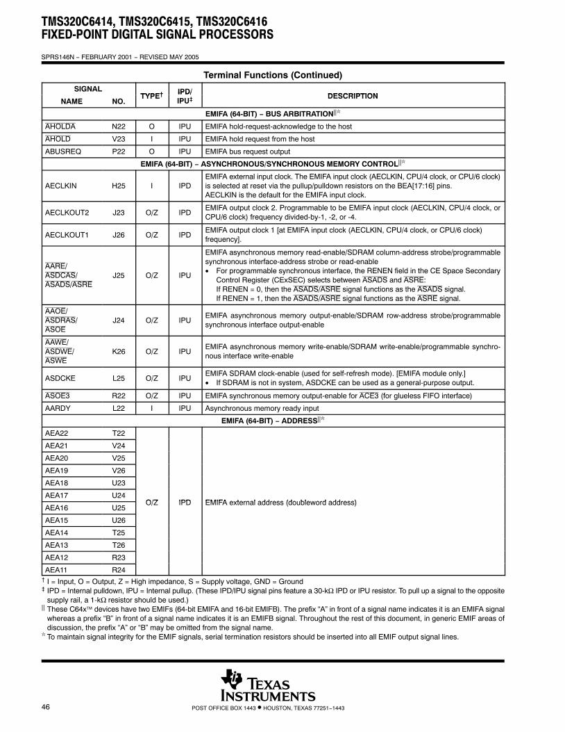
TMS320C6414, TMS320C6415, TMS320C6416FIXED-POINT DIGITAL SIGNAL PROCESSORS
SPRS146N − FEBRUARY 2001 − REVISED MAY 2005
46 POST OFFICE BOX 1443 • HOUSTON, TEXAS 77251−1443
Terminal Functions (Continued)SIGNAL
TYPE† IPD/DESCRIPTION
NAME NO.TYPE† IPD/
IPU‡ DESCRIPTION
EMIFA (64-BIT) − BUS ARBITRATION||
AHOLDA N22 O IPU EMIFA hold-request-acknowledge to the host
AHOLD V23 I IPU EMIFA hold request from the host
ABUSREQ P22 O IPU EMIFA bus request output
EMIFA (64-BIT) − ASYNCHRONOUS/SYNCHRONOUS MEMORY CONTROL||
AECLKIN H25 I IPDEMIFA external input clock. The EMIFA input clock (AECLKIN, CPU/4 clock, or CPU/6 clock)is selected at reset via the pullup/pulldown resistors on the BEA[17:16] pins.AECLKIN is the default for the EMIFA input clock.
AECLKOUT2 J23 O/Z IPDEMIFA output clock 2. Programmable to be EMIFA input clock (AECLKIN, CPU/4 clock, orCPU/6 clock) frequency divided-by-1, -2, or -4.
AECLKOUT1 J26 O/Z IPDEMIFA output clock 1 [at EMIFA input clock (AECLKIN, CPU/4 clock, or CPU/6 clock)frequency].
AARE/ASDCAS/ASADS/ASRE
J25 O/Z IPU
EMIFA asynchronous memory read-enable/SDRAM column-address strobe/programmablesynchronous interface-address strobe or read-enable• For programmable synchronous interface, the RENEN field in the CE Space Secondary
Control Register (CExSEC) selects between ASADS and ASRE:If RENEN = 0, then the ASADS/ASRE signal functions as the ASADS signal.If RENEN = 1, then the ASADS/ASRE signal functions as the ASRE signal.
AAOE/ASDRAS/ASOE
J24 O/Z IPUEMIFA asynchronous memory output-enable/SDRAM row-address strobe/programmablesynchronous interface output-enable
AAWE/ASDWE/ASWE
K26 O/Z IPUEMIFA asynchronous memory write-enable/SDRAM write-enable/programmable synchro-nous interface write-enable
ASDCKE L25 O/Z IPUEMIFA SDRAM clock-enable (used for self-refresh mode). [EMIFA module only.]• If SDRAM is not in system, ASDCKE can be used as a general-purpose output.
ASOE3 R22 O/Z IPU EMIFA synchronous memory output-enable for ACE3 (for glueless FIFO interface)
AARDY L22 I IPU Asynchronous memory ready input
EMIFA (64-BIT) − ADDRESS||
AEA22 T22
AEA21 V24
AEA20 V25
AEA19 V26
AEA18 U23
AEA17 U24O/Z IPD EMIFA external address (doubleword address)
AEA16 U25O/Z IPD EMIFA external address (doubleword address)
AEA15 U26
AEA14 T25
AEA13 T26
AEA12 R23
AEA11 R24† I = Input, O = Output, Z = High impedance, S = Supply voltage, GND = Ground‡ IPD = Internal pulldown, IPU = Internal pullup. (These IPD/IPU signal pins feature a 30-kΩ IPD or IPU resistor. To pull up a signal to the opposite
supply rail, a 1-kΩ resistor should be used.)|| These C64x™ devices have two EMIFs (64-bit EMIFA and 16-bit EMIFB). The prefix “A” in front of a signal name indicates it is an EMIFA signal
whereas a prefix “B” in front of a signal name indicates it is an EMIFB signal. Throughout the rest of this document, in generic EMIF areas ofdiscussion, the prefix “A” or “B” may be omitted from the signal name.
To maintain signal integrity for the EMIF signals, serial termination resistors should be inserted into all EMIF output signal lines.

TMS320C6414, TMS320C6415, TMS320C6416FIXED-POINT DIGITAL SIGNAL PROCESSORS
SPRS146N − FEBRUARY 2001 − REVISED MAY 2005
47POST OFFICE BOX 1443 • HOUSTON, TEXAS 77251−1443
Terminal Functions (Continued)SIGNAL
TYPE† IPD/DESCRIPTION
NAME NO.TYPE† IPD/
IPU‡ DESCRIPTION
EMIFA (64-BIT) − ADDRESS|| (CONTINUED)
AEA10 P23
AEA9 P24
AEA8 P26
AEA7 N23O/Z IPD EMIFA external address (doubleword address)
AEA6 N24O/Z IPD EMIFA external address (doubleword address)
AEA5 N26
AEA4 M23
AEA3 M24
EMIFA (64-bit) − DATA||
AED63 AF24
AED62 AF23
AED61 AE23
AED60 AE22
AED59 AD22
AED58 AF22
AED57 AD21
AED56 AE21
AED55 AC21
AED54 AF21
AED53 AD20
AED52 AE20
AED51 AC20
AED50 AF20 I/O/Z IPU EMIFA external data
AED49 AC19
I/O/Z IPU EMIFA external data
AED48 AD19
AED47 W24
AED46 W23
AED45 Y26
AED44 Y23
AED43 Y25
AED42 Y24
AED41 AA26
AED40 AA23
AED39 AA25
AED38 AA24
AED37 AB26† I = Input, O = Output, Z = High impedance, S = Supply voltage, GND = Ground‡ IPD = Internal pulldown, IPU = Internal pullup. (These IPD/IPU signal pins feature a 30-kΩ IPD or IPU resistor. To pull up a signal to the opposite
supply rail, a 1-kΩ resistor should be used.)|| These C64x™ devices have two EMIFs (64-bit EMIFA and 16-bit EMIFB). The prefix “A” in front of a signal name indicates it is an EMIFA signal
whereas a prefix “B” in front of a signal name indicates it is an EMIFB signal. Throughout the rest of this document, in generic EMIF areas ofdiscussion, the prefix “A” or “B” may be omitted from the signal name.
To maintain signal integrity for the EMIF signals, serial termination resistors should be inserted into all EMIF output signal lines.
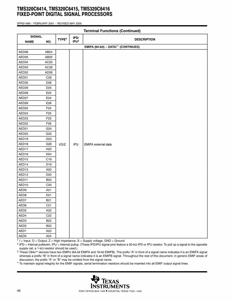
TMS320C6414, TMS320C6415, TMS320C6416FIXED-POINT DIGITAL SIGNAL PROCESSORS
SPRS146N − FEBRUARY 2001 − REVISED MAY 2005
48 POST OFFICE BOX 1443 • HOUSTON, TEXAS 77251−1443
Terminal Functions (Continued)SIGNAL
TYPE† IPD/DESCRIPTION
NAME NO.TYPE† IPD/
IPU‡ DESCRIPTION
EMIFA (64-bit) − DATA|| (CONTINUED)
AED36 AB24
AED35 AB25
AED34 AC25
AED33 AC26
AED32 AD26
AED31 C26
AED30 D26
AED29 D25
AED28 E25
AED27 E24
AED26 E26
AED25 F24
AED24 F25
AED23 F23
AED22 F26
AED21 G24
AED20 G25
AED19 G23
AED18 G26 I/O/Z IPU EMIFA external data
AED17 H23
I/O/Z IPU EMIFA external data
AED16 H24
AED15 C19
AED14 D19
AED13 A20
AED12 D20
AED11 B20
AED10 C20
AED9 A21
AED8 D21
AED7 B21
AED6 C21
AED5 A22
AED4 C22
AED3 B22
AED2 B23
AED1 A23
AED0 A24† I = Input, O = Output, Z = High impedance, S = Supply voltage, GND = Ground‡ IPD = Internal pulldown, IPU = Internal pullup. (These IPD/IPU signal pins feature a 30-kΩ IPD or IPU resistor. To pull up a signal to the opposite
supply rail, a 1-kΩ resistor should be used.)|| These C64x™ devices have two EMIFs (64-bit EMIFA and 16-bit EMIFB). The prefix “A” in front of a signal name indicates it is an EMIFA signal
whereas a prefix “B” in front of a signal name indicates it is an EMIFB signal. Throughout the rest of this document, in generic EMIF areas ofdiscussion, the prefix “A” or “B” may be omitted from the signal name.
To maintain signal integrity for the EMIF signals, serial termination resistors should be inserted into all EMIF output signal lines.

TMS320C6414, TMS320C6415, TMS320C6416FIXED-POINT DIGITAL SIGNAL PROCESSORS
SPRS146N − FEBRUARY 2001 − REVISED MAY 2005
49POST OFFICE BOX 1443 • HOUSTON, TEXAS 77251−1443
Terminal Functions (Continued)SIGNAL
TYPE† IPD/DESCRIPTION
NAME NO.TYPE† IPD/
IPU‡ DESCRIPTION
EMIFB (16-bit) − CONTROL SIGNALS COMMON TO ALL TYPES OF MEMORY||
BCE3 A13 O/Z IPU
BCE2 C12 O/Z IPU EMIFB memory space enables• Enabled by bits 26 through 31 of the word address
BCE1 B12 O/Z IPU• Enabled by bits 26 through 31 of the word address• Only one pin is asserted during any external data access
BCE0 A12 O/Z IPU• Only one pin is asserted during any external data access
BBE1 D13 O/Z IPUEMIFB byte-enable control• Decoded from the low-order address bits. The number of address bits or byte enables
used depends on the width of external memory
BBE0 C13 O/Z IPU
used depends on the width of external memory.• Byte-write enables for most types of memory• Can be directly connected to SDRAM read and write mask signal (SDQM)
BPDT E12 O/Z IPU EMIFB peripheral data transfer, allows direct transfer between external peripherals
EMIFB (16-BIT) − BUS ARBITRATION||
BHOLDA E13 O IPU EMIFB hold-request-acknowledge to the host
BHOLD B19 I IPU EMIFB hold request from the host
BBUSREQ E14 O IPU EMIFB bus request output
EMIFB (16-BIT) − ASYNCHRONOUS/SYNCHRONOUS MEMORY CONTROL||
BECLKIN A11 I IPDEMIFB external input clock. The EMIFB input clock (BECLKIN, CPU/4 clock, or CPU/6 clock)is selected at reset via the pullup/pulldown resistors on the BEA[15:14] pins.BECLKIN is the default for the EMIFB input clock.
BECLKOUT2 D11 O/Z IPDEMIFB output clock 2. Programmable to be EMIFB input clock (BECLKIN, CPU/4 clock, orCPU/6 clock) frequency divided by 1, 2, or 4.
BECLKOUT1 D12 O/Z IPDEMIFB output clock 1 [at EMIFB input clock (BECLKIN, CPU/4 clock, or CPU/6 clock) frequency].
BARE/BSDCAS/BSADS/BSRE
A10 O/Z IPU
EMIFB asynchronous memory read-enable/SDRAM column-address strobe/programmablesynchronous interface-address strobe or read-enable• For programmable synchronous interface, the RENEN field in the CE Space Secondary
Control Register (CExSEC) selects between BSADS and BSRE:If RENEN = 0, then the BSADS/BSRE signal functions as the BSADS signal.If RENEN = 1, then the BSADS/BSRE signal functions as the BSRE signal.
BAOE/BSDRAS/BSOE
B11 O/Z IPUEMIFB asynchronous memory output-enable/SDRAM row-address strobe/programmablesynchronous interface output-enable
BAWE/BSDWE/BSWE
C11 O/Z IPUEMIFB asynchronous memory write-enable/SDRAM write-enable/programmable synchro-nous interface write-enable
BSOE3 E15 O/Z IPU EMIFB synchronous memory output enable for BCE3 (for glueless FIFO interface)
BARDY E11 I IPU EMIFB asynchronous memory ready input† I = Input, O = Output, Z = High impedance, S = Supply voltage, GND = Ground‡ IPD = Internal pulldown, IPU = Internal pullup. (These IPD/IPU signal pins feature a 30-kΩ IPD or IPU resistor. To pull up a signal to the opposite
supply rail, a 1-kΩ resistor should be used.)|| These C64x™ devices have two EMIFs (64-bit EMIFA and 16-bit EMIFB). The prefix “A” in front of a signal name indicates it is an EMIFA signal
whereas a prefix “B” in front of a signal name indicates it is an EMIFB signal. Throughout the rest of this document, in generic EMIF areas ofdiscussion, the prefix “A” or “B” may be omitted from the signal name.
To maintain signal integrity for the EMIF signals, serial termination resistors should be inserted into all EMIF output signal lines.

TMS320C6414, TMS320C6415, TMS320C6416FIXED-POINT DIGITAL SIGNAL PROCESSORS
SPRS146N − FEBRUARY 2001 − REVISED MAY 2005
50 POST OFFICE BOX 1443 • HOUSTON, TEXAS 77251−1443
Terminal Functions (Continued)SIGNAL
TYPE† IPD/DESCRIPTION
NAME NO.TYPE† IPD/
IPU‡ DESCRIPTION
EMIFB (16-BIT) − ADDRESS||
BEA20 E16 IPUEMIFB external address (half-word address) (O/Z)• Also controls initialization of DSP modes at reset (I) via pullup/pulldown resistors
D i E di dBEA19 D18 IPU
− Device Endian modeBEA20: 0 – Big Endian
1 − Little Endian (default mode)
BEA18 C18
1 − Little Endian (default mode)− Boot mode
BEA[19:18]: 00 – No boot
BEA17 B18
BEA[19:18]: 00 No boot01 − HPI boot10 − EMIFB 8-bit ROM boot with default timings (default mode)11 Reserved
BEA16 A18
11 − Reserved
− EMIF clock select
BEA15 D17
− EMIF clock selectBEA[17:16]: Clock mode select for EMIFA (AECLKIN_SEL[1:0])
00 – AECLKIN (default mode)01 CPU/4 Cl k R t
BEA14 C1701 − CPU/4 Clock Rate10 − CPU/6 Clock Rate11 − Reserved
BEA13 B17
11 − Reserved
BEA[15:14]: Clock mode select for EMIFB (BECLKIN_SEL[1:0])
BEA12 A17
[ ] ( _ [ ])00 – BECLKIN (default mode)01 − CPU/4 Clock Rate10 − CPU/6 Clock Rate
BEA11 D16
10 − CPU/6 Clock Rate11 − Reserved
BEA10 C16
I/O/Z IPD
− PCI EEPROM Auto-Initialization (EEAI) [C6415 and C6416 devices only]BEA13: PCI auto-initialization via external EEPROMIf the PCI peripheral is disabled (PCI EN pin 0) this pin must not be pulled up
BEA9 B16
I/O/Z IPD If the PCI peripheral is disabled (PCI_EN pin = 0), this pin must not be pulled up.0 − PCI auto-initialization through EEPROM is disabled (default).1 − PCI auto-initialization through EEPROM is enabled.
BEA8 A16
1 − PCI auto-initialization through EEPROM is enabled.
− UTOPIA Enable (UTOPIA_EN) [C6415 and C6416 devices only]BEA UTOPIA i h l bl (f i l)
BEA7 D15
( _ ) [ y]BEA11: UTOPIA peripheral enable (functional)
0 − UTOPIA disabled (McBSP1 enabled) [default]1 − UTOPIA enabled (McBSP1 disabled)
BEA6 C15
1 − UTOPIA enabled (McBSP1 disabled)
The C6414 device does not support the PCI and UTOPIA peripherals; for proper device
BEA5 B15
The C6414 device does not support the PCI and UTOPIA peripherals; for proper device operation, do not oppose the internal pulldowns (IPDs) on the BEA13 and BEA11 pins.
Also for proper C6414 device operation do not oppose the IPDs on the BEA7 BEA8BEA4 A15
Also for proper C6414 device operation, do not oppose the IPDs on the BEA7, BEA8,and BEA9 pins.
BEA3 D14For proper C6415 device operation, the BEA7 pin must be externally pulled up with a1-kΩ resistor.
BEA2 C14 For proper C6416 device operation, the BEA8 and BEA9 pins must be externally pulledup with a 1-kΩ resistor.
BEA1 A14
up with a 1-kΩ resistor.
For more details, see the Device Configurations section of this data sheet.† I = Input, O = Output, Z = High impedance, S = Supply voltage, GND = Ground‡ IPD = Internal pulldown, IPU = Internal pullup. (These IPD/IPU signal pins feature a 30-kΩ IPD or IPU resistor. To pull up a signal to the opposite
supply rail, a 1-kΩ resistor should be used.)|| These C64x™ devices have two EMIFs (64-bit EMIFA and 16-bit EMIFB). The prefix “A” in front of a signal name indicates it is an EMIFA signal
whereas a prefix “B” in front of a signal name indicates it is an EMIFB signal. Throughout the rest of this document, in generic EMIF areas ofdiscussion, the prefix “A” or “B” may be omitted from the signal name.
To maintain signal integrity for the EMIF signals, serial termination resistors should be inserted into all EMIF output signal lines.

TMS320C6414, TMS320C6415, TMS320C6416FIXED-POINT DIGITAL SIGNAL PROCESSORS
SPRS146N − FEBRUARY 2001 − REVISED MAY 2005
51POST OFFICE BOX 1443 • HOUSTON, TEXAS 77251−1443
Terminal Functions (Continued)SIGNAL
TYPE† IPD/DESCRIPTION
NAME NO.TYPE† IPD/
IPU‡ DESCRIPTION
EMIFB (16-bit) − DATA||
BED15 D7
BED14 B6
BED13 C7
BED12 A6
BED11 D8
BED10 B7
BED9 C8
BED8 A7I/O/Z IPU EMIFB external data
BED7 C9I/O/Z IPU EMIFB external data
BED6 B8
BED5 D9
BED4 B9
BED3 C10
BED2 A9
BED1 D10
BED0 B10
MULTICHANNEL BUFFERED SERIAL PORT 2 (McBSP2)
MCBSP2_EN AF3 I IPDMcBSP2 enable pin. This pin works in conjunction with the PCI_EN pin to enable/disable otherperipherals (for more details, see the Device Configurations section of this data sheet).
CLKS2/GP8§ AE4 I/O/Z IPDMcBSP2 external clock source (CLKS2) [input only] [default] or this pin can also be programmed as a GPIO 8 pin (I/O/Z).
CLKR2 AB1 I/O/Z IPDMcBSP2 receive clock. When McBSP2 is disabled (PCI_EN = 1 and MCBSP2_EN pin = 0),this pin is tied-off.
CLKX2/XSP_CLK§ AC2 I/O/Z IPD McBSP2 transmit clock (I/O/Z) [default] or PCI serial interface clock (O).
DR2/XSP_DI§ AB3 I IPUMcBSP2 receive data (I) [default] or PCI serial interface data in (I). In PCI mode, this pin isconnected to the output data pin of the serial PROM.
DX2/XSP_DO§ AA2 O/Z IPUMcBSP2 transmit data (O/Z) [default] or PCI serial interface data out (O). In PCI mode, this pinis connected to the input data pin of the serial PROM.
FSR2 AC1 I/O/Z IPDMcBSP2 receive frame sync. When McBSP2 is disabled (PCI_EN = 1 and MCBSP2_EN pin = 0), this pin is tied-off.
FSX2 AB2 I/O/Z IPDMcBSP2 transmit frame sync. When McBSP2 is disabled (PCI_EN = 1 and MCBSP2_EN pin = 0), this pin is tied-off.
† I = Input, O = Output, Z = High impedance, S = Supply voltage, GND = Ground‡ IPD = Internal pulldown, IPU = Internal pullup. (These IPD/IPU signal pins feature a 30-kΩ IPD or IPU resistor. To pull up a signal to the opposite
supply rail, a 1-kΩ resistor should be used.)§ For the C6415 and C6416 devices, these pins are multiplexed pins. For more details, see the Device Configurations section of this data sheet.
The C6414 device does not support the PCI or UTOPIA peripherals; therefore, these muxed peripheral pins except CLKS2/GP8 are standaloneperipheral functions for this device.
|| These C64x™ devices have two EMIFs (64-bit EMIFA and 16-bit EMIFB). The prefix “A” in front of a signal name indicates it is an EMIFA signalwhereas a prefix “B” in front of a signal name indicates it is an EMIFB signal. Throughout the rest of this document, in generic EMIF areas ofdiscussion, the prefix “A” or “B” may be omitted from the signal name.
To maintain signal integrity for the EMIF signals, serial termination resistors should be inserted into all EMIF output signal lines.

TMS320C6414, TMS320C6415, TMS320C6416FIXED-POINT DIGITAL SIGNAL PROCESSORS
SPRS146N − FEBRUARY 2001 − REVISED MAY 2005
52 POST OFFICE BOX 1443 • HOUSTON, TEXAS 77251−1443
Terminal Functions (Continued)SIGNAL
TYPE† IPD/DESCRIPTION
NAME NO.TYPE† IPD/
IPU‡ DESCRIPTION
MULTICHANNEL BUFFERED SERIAL PORT 1 (McBSP1)
CLKS1/URADDR3§ AC8 I
McBSP1 external clock source (as opposed to internal) (I) [default] or UTOPIA receiveaddress 3 pin (I)
CLKR1/URADDR2§ AC10 I/O/Z McBSP1 receive clock (I/O/Z) [default] or UTOPIA receive address 2 pin (I)
CLKX1/URADDR4§ AB12 I/O/Z McBSP1 transmit clock (I/O/Z) [default] or UTOPIA receive address 4 pin (I)
DR1/UXADDR1§ AF11 I McBSP1 receive data (I) [default] or UTOPIA transmit address 1 pin (I)
DX1/UXADDR4§ AB11 I/O/Z McBSP1 transmit data (O/Z) [default] or UTOPIA transmit address 4 pin (I)
FSR1/UXADDR2§ AC9 I/O/Z McBSP1 receive frame sync (I/O/Z) [default] or UTOPIA transmit address 2 pin (I)
FSX1/UXADDR3§ AB13 I/O/Z McBSP1 transmit frame sync (I/O/Z) [default] or UTOPIA transmit address 3 pin (I)
MULTICHANNEL BUFFERED SERIAL PORT 0 (McBSP0)
CLKS0 F4 I IPD McBSP0 external clock source (as opposed to internal)
CLKR0 D1 I/O/Z IPD McBSP0 receive clock
CLKX0 E1 I/O/Z IPD McBSP0 transmit clock
DR0 D2 I IPU McBSP0 receive data
DX0 E2 O/Z IPU McBSP0 transmit data
FSR0 C1 I/O/Z IPD McBSP0 receive frame sync
FSX0 E3 I/O/Z IPD McBSP0 transmit frame sync
TIMER 2
TOUT2Φ A4 O/Z IPD Timer 2 or general-purpose output
TINP2 C5 I IPD Timer 2 or general-purpose input
TIMER 1
TOUT1Φ B5 O/Z IPD Timer 1 or general-purpose output
TINP1 A5 I IPD Timer 1 or general-purpose input
TIMER 0
TOUT0Φ D6 O/Z IPD Timer 0 or general-purpose output
TINP0 C6 I IPD Timer 0 or general-purpose input† I = Input, O = Output, Z = High impedance, S = Supply voltage, GND = Ground‡ IPD = Internal pulldown, IPU = Internal pullup. (These IPD/IPU signal pins feature a 30-kΩ IPD or IPU resistor. To pull up a signal to the opposite
supply rail, a 1-kΩ resistor should be used.)§ For the C6415 and C6416 devices, these pins are multiplexed pins. For more details, see the Device Configurations section of this data sheet.
The C6414 device does not support the PCI or UTOPIA peripherals; therefore, these muxed peripheral pins are standalone peripheral functionsfor this device.
ΦFollowing RESET, TOUTx will be configured as a general-purpose output (GPO) due to the default value of the Timerx Control Register (CTLx);therefore, an external resistor may not be used to pull the signal to the opposite supply rail.

TMS320C6414, TMS320C6415, TMS320C6416FIXED-POINT DIGITAL SIGNAL PROCESSORS
SPRS146N − FEBRUARY 2001 − REVISED MAY 2005
53POST OFFICE BOX 1443 • HOUSTON, TEXAS 77251−1443
Terminal Functions (Continued)SIGNAL
TYPE† IPD/DESCRIPTION
NAME NO.TYPE† IPD/
IPU‡ DESCRIPTION
UNIVERSAL TEST AND OPERATIONS PHY INTERFACE FOR ASYNCHRONOUS TRANSFER MODE (ATM) [UTOPIA SLAVE][C6415 and C6416 devices only]
UTOPIA SLAVE (ATM CONTROLLER) − TRANSMIT INTERFACE
UXCLK AD11 I Source clock for UTOPIA transmit driven by Master ATM Controller. When the UTOPIA peripheral is disabled (UTOPIA_EN [BEA11 pin] = 0), this pin is tied-off.
UXCLAV AC14 O/Z
Transmit cell available status output signal from UTOPIA Slave. 0 indicates a complete cell is NOT available for transmit1 indicates a complete cell is available for transmit
When the UTOPIA peripheral is disabled (UTOPIA_EN [BEA11 pin] = 0), this pin is tied-off.
UXENB AE15 I ◊
UTOPIA transmit interface enable input signal. Asserted by the Master ATM Controller to indi-cate that the UTOPIA Slave should put out on the Transmit Data Bus the first byte of valid dataand the UXSOC signal in the next clock cycle.When the UTOPIA peripheral is disabled (UTOPIA_EN [BEA11 pin] = 0), this pin is tied-off.
UXSOC AC13 O/Z
Transmit Start-of-Cell signal. This signal is output by the UTOPIA Slave on the rising edge ofthe UXCLK, indicating that the first valid byte of the cell is available on the 8-bit Transmit DataBus (UXDATA[7:0]).When the UTOPIA peripheral is disabled (UTOPIA_EN [BEA11 pin] = 0), this pin is tied-off.
DX1/UXADDR4§ AB11 I/O/Z ◊
McBSP1 [default] or UTOPIA transmit address pins
As UTOPIA transmit address pins UXADDR[4:0] (I), UTOPIA_EN (BEA11 pin) = 1:• 5-bit Slave transmit address input pins driven by the Master ATM Controller to identify and
select one of the Slave devices (up to 31 possible) in the ATM System.
• UXADDR0 pin is tied off when the UTOPIA peripheral is disabled [UTOPIA_EN (BEA11 pin) = 0]
For the McBSP1 pin functions (UTOPIA_EN (BEA11 pin) = 0 [default]), see the MULTICHAN-NEL BUFFERED SERIAL PORT 1 (McBSP1) section of this table.
FSX1/UXADDR3§ AB13 I/O/Z ◊
McBSP1 [default] or UTOPIA transmit address pins
As UTOPIA transmit address pins UXADDR[4:0] (I), UTOPIA EN (BEA11 pin) = 1:
FSR1/UXADDR2§ AC9 I/O/Z ◊
As UTOPIA transmit address pins UXADDR[4:0] (I), UTOPIA_EN (BEA11 pin) = 1:• 5-bit Slave transmit address input pins driven by the Master ATM Controller to identify and
select one of the Slave devices (up to 31 possible) in the ATM System.
DR1/UXADDR1§ AF11 I ◊
• UXADDR0 pin is tied off when the UTOPIA peripheral is disabled [UTOPIA_EN (BEA11 pin) = 0]
UXADDR0 AE9 I ◊For the McBSP1 pin functions (UTOPIA_EN (BEA11 pin) = 0 [default]), see the MULTICHAN-NEL BUFFERED SERIAL PORT 1 (McBSP1) section of this table.
† I = Input, O = Output, Z = High impedance, S = Supply voltage, GND = Ground‡ IPD = Internal pulldown, IPU = Internal pullup. (These IPD/IPU signal pins feature a 30-kΩ IPD or IPU resistor. To pull up a signal to the opposite
supply rail, a 1-kΩ resistor should be used.)§ For the C6415 and C6416 devices, these pins are multiplexed pins. For more details, see the Device Configurations section of this data sheet.
The C6414 device does not support the PCI or UTOPIA peripherals; therefore, these muxed peripheral pins are standalone peripheral functionsfor this device.
For the C6415 and C6416 devices, external pulldowns required: If UTOPIA is selected (BEA11 = 1) and these pins are connected to other devices,then a 10-kΩ resistor must be used to externally pull down each of these pins. If these pins are “no connects”, then only UXCLK and URCLKneed to be pulled down and other pulldowns are not necessary.
◊ For the C6415 and C6416 devices, external pullups required: If UTOPIA is selected (BEA11 = 1) and these pins are connected to other devices,then a 10-kΩ resistor must be used to externally pull up each of these pins. If these pins are “no connects”, then the pullups are not necessary.
ΨThe C6414 device does not support the UTOPIA peripheral; therefore, these standalone UTOPIA pins are Reserved (leave unconnected, donot connect to power or ground) with the exception of UXCLK and URCLK which should be connected to a 10-kΩ pulldown resistor (see thesquare [] footnote).
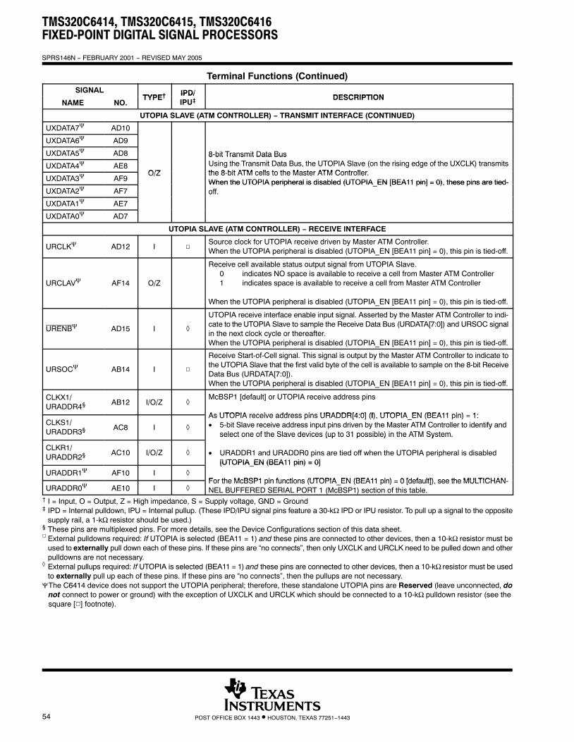
TMS320C6414, TMS320C6415, TMS320C6416FIXED-POINT DIGITAL SIGNAL PROCESSORS
SPRS146N − FEBRUARY 2001 − REVISED MAY 2005
54 POST OFFICE BOX 1443 • HOUSTON, TEXAS 77251−1443
Terminal Functions (Continued)SIGNAL
TYPE† IPD/DESCRIPTION
NAME NO.TYPE† IPD/
IPU‡ DESCRIPTION
UTOPIA SLAVE (ATM CONTROLLER) − TRANSMIT INTERFACE (CONTINUED)
UXDATA7 AD10
UXDATA6 AD9
UXDATA5 AD8 8-bit Transmit Data Bus
UXDATA4 AE8O/Z
8 bit Transmit Data BusUsing the Transmit Data Bus, the UTOPIA Slave (on the rising edge of the UXCLK) transmitsthe 8 bit ATM cells to the Master ATM Controller
UXDATA3 AF9O/Z the 8-bit ATM cells to the Master ATM Controller.
When the UTOPIA peripheral is disabled (UTOPIA EN [BEA11 pin] = 0), these pins are tied-UXDATA2 AF7
When the UTOPIA peripheral is disabled (UTOPIA_EN [BEA11 pin] = 0), these pins are tied-off.
UXDATA1 AE7
off.
UXDATA0 AD7
UTOPIA SLAVE (ATM CONTROLLER) − RECEIVE INTERFACE
URCLK AD12 I Source clock for UTOPIA receive driven by Master ATM Controller. When the UTOPIA peripheral is disabled (UTOPIA_EN [BEA11 pin] = 0), this pin is tied-off.
URCLAV AF14 O/Z
Receive cell available status output signal from UTOPIA Slave. 0 indicates NO space is available to receive a cell from Master ATM Controller1 indicates space is available to receive a cell from Master ATM Controller
When the UTOPIA peripheral is disabled (UTOPIA_EN [BEA11 pin] = 0), this pin is tied-off.
URENB AD15 I ◊
UTOPIA receive interface enable input signal. Asserted by the Master ATM Controller to indi-cate to the UTOPIA Slave to sample the Receive Data Bus (URDATA[7:0]) and URSOC signalin the next clock cycle or thereafter.When the UTOPIA peripheral is disabled (UTOPIA_EN [BEA11 pin] = 0), this pin is tied-off.
URSOC AB14 I
Receive Start-of-Cell signal. This signal is output by the Master ATM Controller to indicate tothe UTOPIA Slave that the first valid byte of the cell is available to sample on the 8-bit ReceiveData Bus (URDATA[7:0]).When the UTOPIA peripheral is disabled (UTOPIA_EN [BEA11 pin] = 0), this pin is tied-off.
CLKX1/URADDR4§ AB12 I/O/Z ◊
McBSP1 [default] or UTOPIA receive address pins
As UTOPIA receive address pins URADDR[4:0] (I) UTOPIA EN (BEA11 pin) 1:CLKS1/URADDR3§ AC8 I ◊
As UTOPIA receive address pins URADDR[4:0] (I), UTOPIA_EN (BEA11 pin) = 1:• 5-bit Slave receive address input pins driven by the Master ATM Controller to identify and
select one of the Slave devices (up to 31 possible) in the ATM System.
CLKR1/URADDR2§ AC10 I/O/Z ◊
select one of the Slave devices (up to 31 possible) in the ATM System.
• URADDR1 and URADDR0 pins are tied off when the UTOPIA peripheral is disabled [UTOPIA EN (BEA11 pin) = 0]
URADDR1 AF10 I ◊[UTOPIA_EN (BEA11 pin) = 0]
For the McBSP1 pin functions (UTOPIA EN (BEA11 pin) 0 [default]) see the MULTICHANURADDR0 AE10 I ◊
For the McBSP1 pin functions (UTOPIA_EN (BEA11 pin) = 0 [default]), see the MULTICHAN-NEL BUFFERED SERIAL PORT 1 (McBSP1) section of this table.
† I = Input, O = Output, Z = High impedance, S = Supply voltage, GND = Ground‡ IPD = Internal pulldown, IPU = Internal pullup. (These IPD/IPU signal pins feature a 30-kΩ IPD or IPU resistor. To pull up a signal to the opposite
supply rail, a 1-kΩ resistor should be used.)§ These pins are multiplexed pins. For more details, see the Device Configurations section of this data sheet. External pulldowns required: If UTOPIA is selected (BEA11 = 1) and these pins are connected to other devices, then a 10-kΩ resistor must be
used to externally pull down each of these pins. If these pins are “no connects”, then only UXCLK and URCLK need to be pulled down and otherpulldowns are not necessary.
◊ External pullups required: If UTOPIA is selected (BEA11 = 1) and these pins are connected to other devices, then a 10-kΩ resistor must be usedto externally pull up each of these pins. If these pins are “no connects”, then the pullups are not necessary.
ΨThe C6414 device does not support the UTOPIA peripheral; therefore, these standalone UTOPIA pins are Reserved (leave unconnected, donot connect to power or ground) with the exception of UXCLK and URCLK which should be connected to a 10-kΩ pulldown resistor (see thesquare [] footnote).
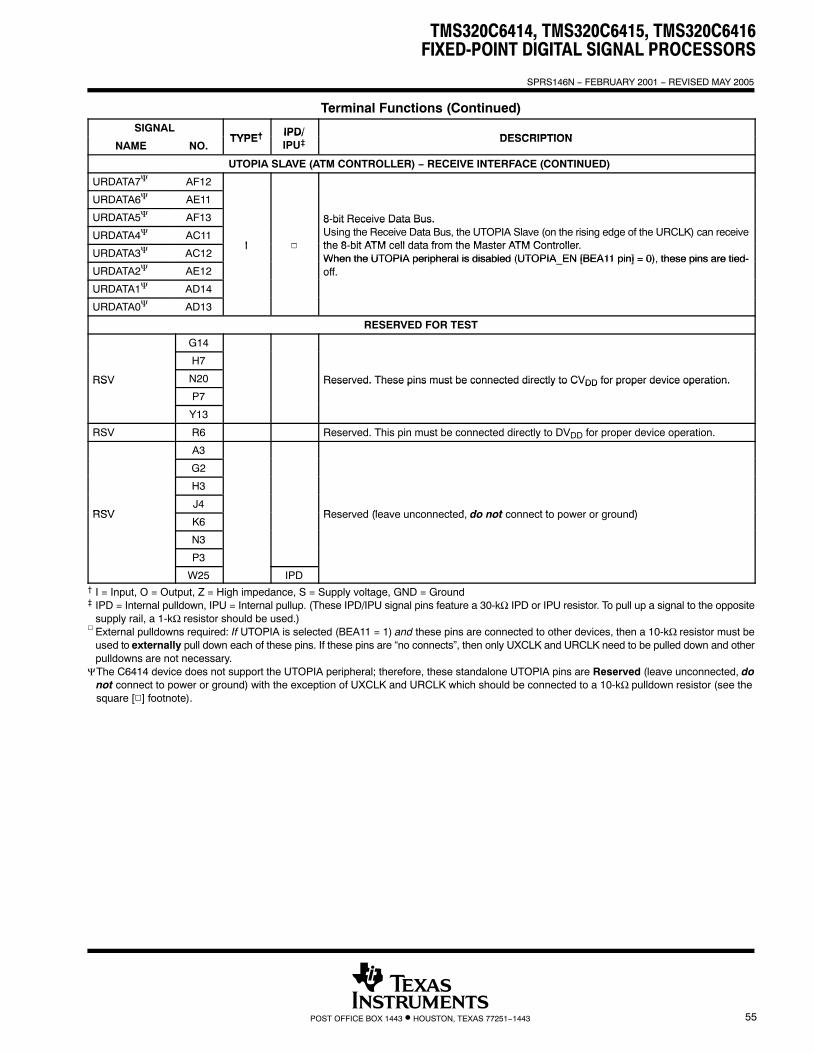
TMS320C6414, TMS320C6415, TMS320C6416FIXED-POINT DIGITAL SIGNAL PROCESSORS
SPRS146N − FEBRUARY 2001 − REVISED MAY 2005
55POST OFFICE BOX 1443 • HOUSTON, TEXAS 77251−1443
Terminal Functions (Continued)SIGNAL
TYPE† IPD/DESCRIPTION
NAME NO.TYPE† IPD/
IPU‡ DESCRIPTION
UTOPIA SLAVE (ATM CONTROLLER) − RECEIVE INTERFACE (CONTINUED)
URDATA7 AF12
URDATA6 AE11
URDATA5 AF13 8-bit Receive Data Bus.
URDATA4 AC11I
8 bit Receive Data Bus.Using the Receive Data Bus, the UTOPIA Slave (on the rising edge of the URCLK) can receivethe 8 bit ATM cell data from the Master ATM Controller
URDATA3 AC12I the 8-bit ATM cell data from the Master ATM Controller.
When the UTOPIA peripheral is disabled (UTOPIA EN [BEA11 pin] = 0), these pins are tied-URDATA2 AE12
When the UTOPIA peripheral is disabled (UTOPIA_EN [BEA11 pin] = 0), these pins are tied-off.
URDATA1 AD14
off.
URDATA0 AD13
RESERVED FOR TEST
G14
H7
RSV N20 Reserved. These pins must be connected directly to CVDD for proper device operation.RSV
P7
Reserved. These pins must be connected directly to CVDD for proper device operation.
Y13
RSV R6 Reserved. This pin must be connected directly to DVDD for proper device operation.
A3
G2
H3
RSVJ4
Reserved (leave unconnected do not connect to power or ground)RSVK6
Reserved (leave unconnected, do not connect to power or ground)
N3
P3
W25 IPD† I = Input, O = Output, Z = High impedance, S = Supply voltage, GND = Ground‡ IPD = Internal pulldown, IPU = Internal pullup. (These IPD/IPU signal pins feature a 30-kΩ IPD or IPU resistor. To pull up a signal to the opposite
supply rail, a 1-kΩ resistor should be used.) External pulldowns required: If UTOPIA is selected (BEA11 = 1) and these pins are connected to other devices, then a 10-kΩ resistor must be
used to externally pull down each of these pins. If these pins are “no connects”, then only UXCLK and URCLK need to be pulled down and otherpulldowns are not necessary.
ΨThe C6414 device does not support the UTOPIA peripheral; therefore, these standalone UTOPIA pins are Reserved (leave unconnected, donot connect to power or ground) with the exception of UXCLK and URCLK which should be connected to a 10-kΩ pulldown resistor (see thesquare [] footnote).
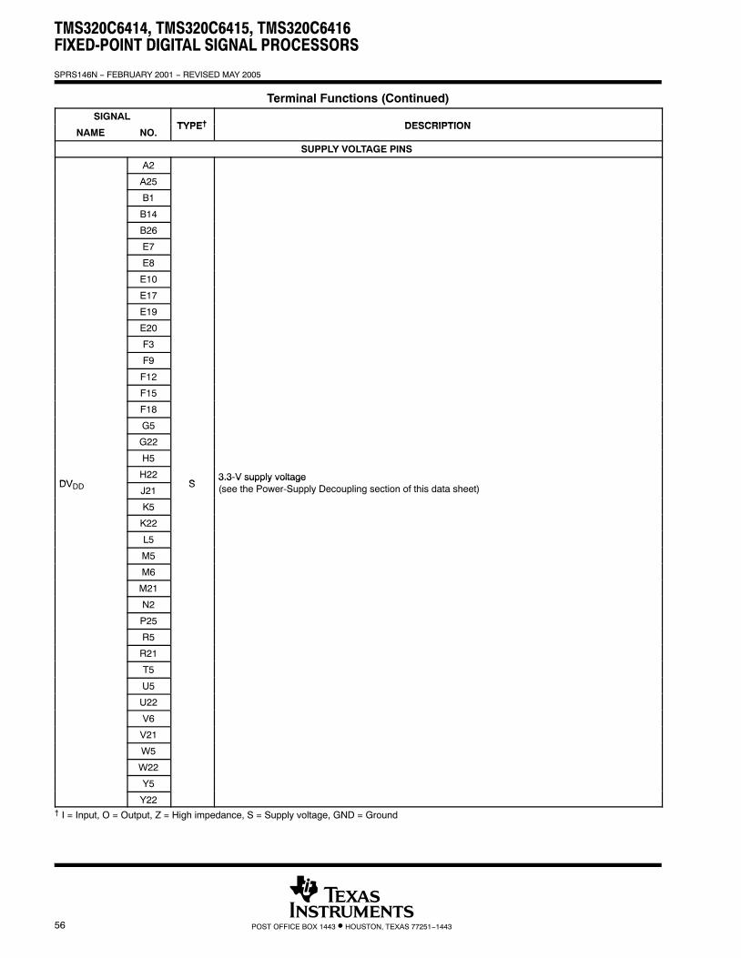
TMS320C6414, TMS320C6415, TMS320C6416FIXED-POINT DIGITAL SIGNAL PROCESSORS
SPRS146N − FEBRUARY 2001 − REVISED MAY 2005
56 POST OFFICE BOX 1443 • HOUSTON, TEXAS 77251−1443
Terminal Functions (Continued)SIGNAL
TYPE† DESCRIPTIONNAME NO.
TYPE† DESCRIPTION
SUPPLY VOLTAGE PINS
A2
A25
B1
B14
B26
E7
E8
E10
E17
E19
E20
F3
F9
F12
F15
F18
G5
G22
H5
DVH22
S3.3-V supply voltage
DVDD J21S
3.3 V supply voltage(see the Power-Supply Decoupling section of this data sheet)
K5
K22
L5
M5
M6
M21
N2
P25
R5
R21
T5
U5
U22
V6
V21
W5
W22
Y5
Y22† I = Input, O = Output, Z = High impedance, S = Supply voltage, GND = Ground

TMS320C6414, TMS320C6415, TMS320C6416FIXED-POINT DIGITAL SIGNAL PROCESSORS
SPRS146N − FEBRUARY 2001 − REVISED MAY 2005
57POST OFFICE BOX 1443 • HOUSTON, TEXAS 77251−1443
Terminal Functions (Continued)SIGNAL
TYPE† DESCRIPTIONNAME NO.
TYPE† DESCRIPTION
SUPPLY VOLTAGE PINS (CONTINUED)
AA9
AA12
AA15
AA18
AB7
AB8
AB103 3 V l lt
DVDD AB173.3-V supply voltage(see the Power-Supply Decoupling section of this data sheet)DVDD
AB19(see the Power-Supply Decoupling section of this data sheet)
AB20
AE1
AE13
AE26
AF2
AF25
A1
A26
B2
B25
C3 S
C24
S
D4
D23
E5
E22
F61 2-V supply voltage (-5E0 device)
CVF7
1.2-V supply voltage (-5E0 device)1.25-V supply voltage (A-5E0 device)
CVDD F201.25-V supply voltage (A-5E0 device)1.4 V supply voltage (-6E3, A-6E3, -7E3 devices) ( th P S l D li ti f thi d t h t)
F21
pp y g ( )(see the Power-Supply Decoupling section of this data sheet)
G6
G7
G8
G10
G11
G13
G16
G17
G19
G20† I = Input, O = Output, Z = High impedance, S = Supply voltage, GND = Ground
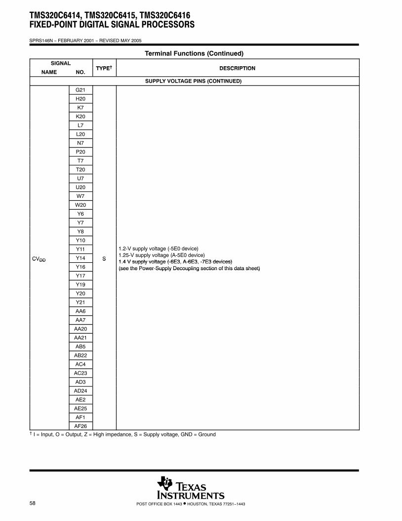
TMS320C6414, TMS320C6415, TMS320C6416FIXED-POINT DIGITAL SIGNAL PROCESSORS
SPRS146N − FEBRUARY 2001 − REVISED MAY 2005
58 POST OFFICE BOX 1443 • HOUSTON, TEXAS 77251−1443
Terminal Functions (Continued)SIGNAL
TYPE† DESCRIPTIONNAME NO.
TYPE† DESCRIPTION
SUPPLY VOLTAGE PINS (CONTINUED)
G21
H20
K7
K20
L7
L20
N7
P20
T7
T20
U7
U20
W7
W20
Y6
Y7
Y8
Y10
Y11 1.2-V supply voltage (-5E0 device)1 25 V l l (A 5E0 d i )
CVDD Y14 S
pp y g ( )1.25-V supply voltage (A-5E0 device)1 4 V supply voltage (-6E3 A-6E3 -7E3 devices) CVDD
Y16
S 1.4 V supply voltage (-6E3, A-6E3, -7E3 devices) (see the Power-Supply Decoupling section of this data sheet)
Y17(see the Power Supply Decoupling section of this data sheet)
Y19
Y20
Y21
AA6
AA7
AA20
AA21
AB5
AB22
AC4
AC23
AD3
AD24
AE2
AE25
AF1
AF26† I = Input, O = Output, Z = High impedance, S = Supply voltage, GND = Ground
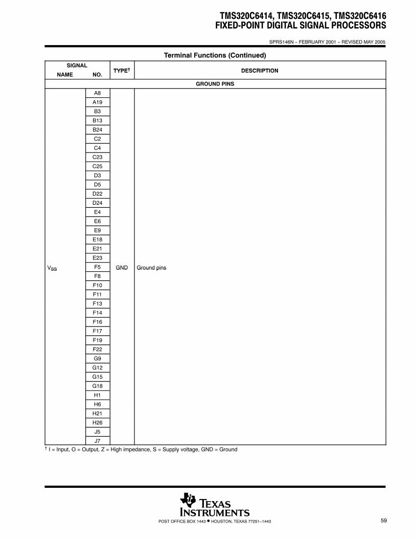
TMS320C6414, TMS320C6415, TMS320C6416FIXED-POINT DIGITAL SIGNAL PROCESSORS
SPRS146N − FEBRUARY 2001 − REVISED MAY 2005
59POST OFFICE BOX 1443 • HOUSTON, TEXAS 77251−1443
Terminal Functions (Continued)SIGNAL
TYPE† DESCRIPTIONNAME NO.
TYPE† DESCRIPTION
GROUND PINS
A8
A19
B3
B13
B24
C2
C4
C23
C25
D3
D5
D22
D24
E4
E6
E9
E18
E21
E23
VSS F5 GND Ground pinsVSS
F8
GND Ground pins
F10
F11
F13
F14
F16
F17
F19
F22
G9
G12
G15
G18
H1
H6
H21
H26
J5
J7† I = Input, O = Output, Z = High impedance, S = Supply voltage, GND = Ground

TMS320C6414, TMS320C6415, TMS320C6416FIXED-POINT DIGITAL SIGNAL PROCESSORS
SPRS146N − FEBRUARY 2001 − REVISED MAY 2005
60 POST OFFICE BOX 1443 • HOUSTON, TEXAS 77251−1443
Terminal Functions (Continued)SIGNAL
TYPE† DESCRIPTIONNAME NO.
TYPE† DESCRIPTION
GROUND PINS (CONTINUED)
J20
J22
K21
L6
L21
M7
M20
N6
N21
N25
P2
P6
P21
R7
R20
T6
T21
U6
U21
VSS V5 GND Ground pinsVSS
V7
GND Ground pins
V20
V22
W1
W6
W21
W26
Y9
Y12
Y15
Y18
AA5
AA8
AA10
AA11
AA13
AA14
AA16
AA17† I = Input, O = Output, Z = High impedance, S = Supply voltage, GND = Ground

TMS320C6414, TMS320C6415, TMS320C6416FIXED-POINT DIGITAL SIGNAL PROCESSORS
SPRS146N − FEBRUARY 2001 − REVISED MAY 2005
61POST OFFICE BOX 1443 • HOUSTON, TEXAS 77251−1443
Terminal Functions (Continued)SIGNAL
TYPE† DESCRIPTIONNAME NO.
TYPE† DESCRIPTION
GROUND PINS (CONTINUED)
AA19
AA22
AB4
AB6
AB9
AB18
AB21
AB23
AC3
AC5
VSS AC22 GND Ground pinsVSS
AC24
GND Ground pins
AD2
AD4
AD23
AD25
AE3
AE14
AE24
AF8
AF19† I = Input, O = Output, Z = High impedance, S = Supply voltage, GND = Ground

TMS320C6414, TMS320C6415, TMS320C6416FIXED-POINT DIGITAL SIGNAL PROCESSORS
SPRS146N − FEBRUARY 2001 − REVISED MAY 2005
62 POST OFFICE BOX 1443 • HOUSTON, TEXAS 77251−1443
development support
TI offers an extensive line of development tools for the TMS320C6000™ DSP platform, including tools toevaluate the performance of the processors, generate code, develop algorithm implementations, and fullyintegrate and debug software and hardware modules.
The following products support development of C6000™ DSP-based applications:
Software Development Tools:Code Composer Studio™ Integrated Development Environment (IDE): including EditorC/C++/Assembly Code Generation, and Debug plus additional development toolsScalable, Real-Time Foundation Software (DSP/BIOS™), which provides the basic run-time target softwareneeded to support any DSP application.
Hardware Development Tools:Extended Development System (XDS™) Emulator (supports C6000™ DSP multiprocessor system debug)EVM (Evaluation Module)
For a complete listing of development-support tools for the TMS320C6000™ DSP platform, visit the TexasInstruments web site on the Worldwide Web at http://www.ti.com uniform resource locator (URL). Forinformation on pricing and availability, contact the nearest TI field sales office or authorized distributor.
Code Composer Studio, DSP/BIOS, and XDS are trademarks of Texas Instruments.

TMS320C6414, TMS320C6415, TMS320C6416FIXED-POINT DIGITAL SIGNAL PROCESSORS
SPRS146N − FEBRUARY 2001 − REVISED MAY 2005
63POST OFFICE BOX 1443 • HOUSTON, TEXAS 77251−1443
device support
device and development-support tool nomenclature
To designate the stages in the product development cycle, TI assigns prefixes to the part numbers of all DSPdevices and support tools. Each DSP commercial family member has one of three prefixes: TMX, TMP, or TMS(i.e., TMS320C6412GTS600) Texas Instruments recommends two of three possible prefix designators for itssupport tools: TMDX and TMDS. These prefixes represent evolutionary stages of product development fromengineering prototypes (TMX/TMDX) through fully qualified production devices/tools (TMS/TMDS).
Device development evolutionary flow:
TMX Experimental device that is not necessarily representative of the final device’s electricalspecifications
TMP Final silicon die that conforms to the device’s electrical specifications but has not completedquality and reliability verification
TMS Fully qualified production device
Support tool development evolutionary flow:
TMDX Development-support product that has not yet completed Texas Instruments internal qualificationtesting
TMDS Fully qualified development-support product
TMX and TMP devices and TMDX development-support tools are shipped against the following disclaimer:
“Developmental product is intended for internal evaluation purposes.”
TMS devices and TMDS development-support tools have been characterized fully, and the quality and reliabilityof the device have been demonstrated fully. TI’s standard warranty applies.
Predictions show that prototype devices (TMX or TMP) have a greater failure rate than the standard productiondevices. Texas Instruments recommends that these devices not be used in any production system because theirexpected end-use failure rate still is undefined. Only qualified production devices are to be used.
TI device nomenclature also includes a suffix with the device family name. This suffix indicates the package type(for example, GLZ), the temperature range (for example, blank is the default commercial temperature range),and the device speed range in megahertz (for example, -6E3 is 600-MHz CPU, 133-MHz EMIFA). Figure 5provides a legend for reading the complete device name for any TMS320C64x™ DSP generation member.
The ZLZ package, like the GLZ package, is a 532-pin plastic BGA only with lead-free soldered balls. The CLZpackage, like the GLZ package, is a 532-pin plastic BGA only with lead-free bump and lead−free soldered balls.The ZLZ and CLZ package types are available upon request. For device part numbers and further orderinginformation for TMS320C6414/C6415/C6416 in the GLZ, ZLZ and CLZ package types, see the TI website(http://www.ti.com) or contact your TI sales representative.

TMS320C6414, TMS320C6415, TMS320C6416FIXED-POINT DIGITAL SIGNAL PROCESSORS
SPRS146N − FEBRUARY 2001 − REVISED MAY 2005
64 POST OFFICE BOX 1443 • HOUSTON, TEXAS 77251−1443
C64x DSP:64116414E 6414D 6414C6415E 6415D 6415C6416E 6416D 6416C
PREFIX DEVICE SPEED RANGE
TMS 32 C 6415E GLZ 6E3
TMX= Experimental deviceTMP= Prototype deviceTMS= Qualified deviceSMX= Experimental device, MILSMJ = MIL-PRF-38535, QMLSM = High Rel (non-38535)
DEVICE FAMILY3 or 32 or 320 = TMS320 DSP family
TECHNOLOGY
PACKAGE TYPE§¶#
GLZ = 532-pin plastic BGAZLZ = 532-pin plastic BGA, Pb−free soldered ballsCLZ = 532-pin plastic BGA, Pb−free bump and Pb−
free soldered ballsC = CMOS DEVICE||
† See the Recommended Operating Conditions section of this data sheet for more details.‡ The extended temperature “A version” devices may have different operating conditions than the commercial temperature devices.§ BGA= Ball Grid Array¶ The ZLZ mechanical package designator represents the version of the GLZ package with Pb-free soldered balls. For more detailed
information, see the Mechanical Data section of this document.# The CLZ mechanical package designator represents the version of the GLZ package with Pb-free bump and soldered balls. For more
detailed information, see the Mechanical Data section of this document.|| For the actual device part numbers (P/Ns) and ordering information, see the TI website (www.ti.com).
TEMPERATURE RANGE (DEFAULT: 0°C TO 90°C)†‡
( )
Blank = 0°C to 90°C, commercial temperatureA = −40°C to 105°C, extended temperature
300 5E0 (500-MHz CPU, 100-MHz EMIF)6E3 (600-MHz CPU, 133-MHz EMIFA)7E3 (720-MHz CPU, 133-MHz EMIFA)
Figure 5. TMS320C64x™ DSP Device Nomenclature (Including the C6414, C6415, and C6416 Devices)
For additional information, see the TMS320C6414, TMS320C6415, and TMS320C6416 Digital SignalProcessors Silicon Errata (literature number SPRZ011)

TMS320C6414, TMS320C6415, TMS320C6416FIXED-POINT DIGITAL SIGNAL PROCESSORS
SPRS146N − FEBRUARY 2001 − REVISED MAY 2005
65POST OFFICE BOX 1443 • HOUSTON, TEXAS 77251−1443
documentation support
Extensive documentation supports all TMS320™ DSP family generations of devices from productannouncement through applications development. The types of documentation available include: data sheets,such as this document, with design specifications; complete user’s reference guides for all devices and tools;technical briefs; development-support tools; on-line help; and hardware and software applications. Thefollowing is a brief, descriptive list of support documentation specific to the C6000™ DSP devices:
The TMS320C6000 CPU and Instruction Set Reference Guide (literature number SPRU189) describes theC6000™ DSP CPU (core) architecture, instruction set, pipeline, and associated interrupts.
The TMS320C6000 DSP Peripherals Overview Reference Guide (literature number SPRU190) provides anoverview and briefly describes the functionality of the peripherals available on the C6000™ DSP platform ofdevices. This document also includes a table listing the peripherals available on the C6000 devices along withliterature numbers and hyperlinks to the associated peripheral documents.
The TMS320C64x Technical Overview (literature number SPRU395) gives an introduction to the C64x™ digitalsignal processor, and discusses the application areas that are enhanced by the C64x™ DSP VelociTI.2™ VLIWarchitecture.
The TMS320C6414, TMS320C6415, and TMS320C6416 Digital Signal Processors Silicon Errata (literaturenumber SPRZ011) describes the known exceptions to the functional specifications for the TMS320C6414,TMS320C6415, and TMS320C6416 devices.
The TMS320C6414/15/16 Power Consumption Summary application report (literature number SPRA811)discusses the power consumption for user applications with the TMS320C6414, TMS320C6415, andTMS320C6416 DSP devices.
The Using IBIS Models for Timing Analysis application report (literature number SPRA839) describes how toproperly use IBIS models to attain accurate timing analysis for a given system.
The How To Begin Development Today With the TMS320C6414, TMS320C6415, and TMS320C6416 DSPsapplication report (literature number SPRA718) describes in more detail the compatibility andsimilarities/differences among the C6414, C6415, C6416, and C6211 devices.
The tools support documentation is electronically available within the Code Composer Studio™ IntegratedDevelopment Environment (IDE). For a complete listing of C6000™ DSP latest documentation, visit the TexasInstruments web site on the Worldwide Web at http://www.ti.com uniform resource locator (URL).
TMS320C6414, TMS320C6415, TMS320C6416FIXED-POINT DIGITAL SIGNAL PROCESSORS
SPRS146N − FEBRUARY 2001 − REVISED MAY 2005
66 POST OFFICE BOX 1443 • HOUSTON, TEXAS 77251−1443
clock PLL
Most of the internal C64x™ DSP clocks are generated from a single source through the CLKIN pin. This sourceclock either drives the PLL, which multiplies the source clock frequency to generate the internal CPU clock, orbypasses the PLL to become the internal CPU clock.
To use the PLL to generate the CPU clock, the external PLL filter circuit must be properly designed. Figure 6shows the external PLL circuitry for either x1 (PLL bypass) or other PLL multiply modes.
To minimize the clock jitter, a single clean power supply should power both the C64x™ DSP device and theexternal clock oscillator circuit. The minimum CLKIN rise and fall times should also be observed. For the inputclock timing requirements, see the input and output clocks electricals section.
Rise/fall times, duty cycles (high/low pulse durations), and the load capacitance of the external clock sourcemust meet the DSP requirements in this data sheet (see the electrical characteristics over recommendedranges of supply voltage and operating case temperature table and the input and output clocks electricalssection). Table 30 lists some examples of compatible CLKIN external clock sources:
Table 30. Compatible CLKIN External Clock Sources
COMPATIBLE PARTS FOREXTERNAL CLOCK SOURCES (CLKIN) PART NUMBER MANUFACTURER
JITO-2 Fox Electronix
OscillatorsSTA series, ST4100 series SaRonix Corporation
OscillatorsSG-636 Epson America
342 Corning Frequency Control
PLL ICS525-02Integrated Circuit Systems
Spread Spectrum Clock Generator MK1714Integrated Circuit Systems

TMS320C6414, TMS320C6415, TMS320C6416FIXED-POINT DIGITAL SIGNAL PROCESSORS
SPRS146N − FEBRUARY 2001 − REVISED MAY 2005
67POST OFFICE BOX 1443 • HOUSTON, TEXAS 77251−1443
clock PLL (continued)
PLLMULT
1
0
PLLCLK
CLKMODE0
CLKMODE1
CLKIN
C2C1EMIfilter
3.3 V
/2
/8
/4
/6
00 01 10
CPU Clock
Peripheral Bus
Timer Internal Clock
CLKOUT4,McBSP Internal Clock
CLKOUT6
ECLKIN_SEL (DEVCFG.[17,16]and DEVCFG.[15,14])
/2
/4
EMIF 00 01 10 EK2RATE(GBLCTL.[19,18])
ECLKOUT2ECLKOUT1
PLLx6, x12
10 µF 0.1 µF
ECLKIN
(For the PLL Options, CLKMODE Pins Setup, andPLL Clock Frequency Ranges, see Table 31.)
Internal to C64x
PLLV
NOTES: A. Place all PLL external components (C1, C2, and the EMI Filter) as close to the C6000™ DSP device as possible. For the bestperformance, TI recommends that all the PLL external components be on a single side of the board without jumpers, switches, orcomponents other than the ones shown.
B. For reduced PLL jitter, maximize the spacing between switching signals and the PLL external components (C1, C2, and the EMIFilter).
C. The 3.3-V supply for the EMI filter must be from the same 3.3-V power plane supplying the I/O voltage, DVDD.D. EMI filter manufacturer TDK part number ACF451832-333, -223, -153, -103. Panasonic part number EXCCET103U.
Figure 6. External PLL Circuitry for Either PLL Multiply Modes or x1 (Bypass) Mode
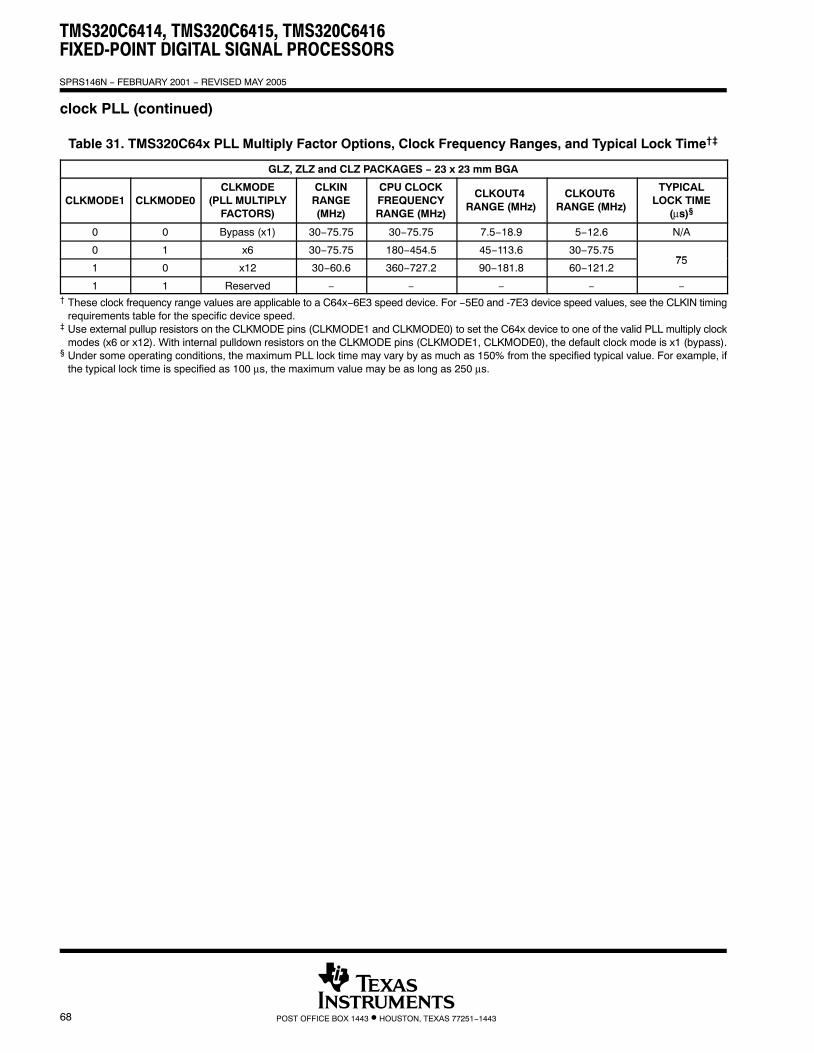
TMS320C6414, TMS320C6415, TMS320C6416FIXED-POINT DIGITAL SIGNAL PROCESSORS
SPRS146N − FEBRUARY 2001 − REVISED MAY 2005
68 POST OFFICE BOX 1443 • HOUSTON, TEXAS 77251−1443
clock PLL (continued)
Table 31. TMS320C64x PLL Multiply Factor Options, Clock Frequency Ranges, and Typical Lock Time†‡
GLZ, ZLZ and CLZ PACKAGES − 23 x 23 mm BGA
CLKMODE1 CLKMODE0CLKMODE
(PLL MULTIPLYFACTORS)
CLKINRANGE(MHz)
CPU CLOCKFREQUENCYRANGE (MHz)
CLKOUT4 RANGE (MHz)
CLKOUT6 RANGE (MHz)
TYPICALLOCK TIME
(µs)§
0 0 Bypass (x1) 30−75.75 30−75.75 7.5−18.9 5−12.6 N/A
0 1 x6 30−75.75 180−454.5 45−113.6 30−75.7575
1 0 x12 30−60.6 360−727.2 90−181.8 60−121.275
1 1 Reserved − − − − −† These clock frequency range values are applicable to a C64x−6E3 speed device. For −5E0 and -7E3 device speed values, see the CLKIN timing
requirements table for the specific device speed.‡ Use external pullup resistors on the CLKMODE pins (CLKMODE1 and CLKMODE0) to set the C64x device to one of the valid PLL multiply clock
modes (x6 or x12). With internal pulldown resistors on the CLKMODE pins (CLKMODE1, CLKMODE0), the default clock mode is x1 (bypass).§ Under some operating conditions, the maximum PLL lock time may vary by as much as 150% from the specified typical value. For example, if
the typical lock time is specified as 100 µs, the maximum value may be as long as 250 µs.

TMS320C6414, TMS320C6415, TMS320C6416FIXED-POINT DIGITAL SIGNAL PROCESSORS
SPRS146N − FEBRUARY 2001 − REVISED MAY 2005
69POST OFFICE BOX 1443 • HOUSTON, TEXAS 77251−1443
general-purpose input/output (GPIO)
To use the GP[15:0] software-configurable GPIO pins, the GPxEN bits in the GP Enable (GPEN) Register andthe GPxDIR bits in the GP Direction (GPDIR) Register must be properly configured.
GPxEN = 1 GP[x] pin is enabled
GPxDIR = 0 GP[x] pin is an input
GPxDIR = 1 GP[x] pin is an output
where “x” represents one of the 15 through 0 GPIO pins
Figure 7 shows the GPIO enable bits in the GPEN register for the C6414/C6415/C6416 device. To use any ofthe GPx pins as general-purpose input/output functions, the corresponding GPxEN bit must be set to “1”(enabled). Default values are device-specific, so refer to Figure 7 for the C6414/15/16 default configuration.
31 24 23 16
Reserved
R-0
15 14 13 12 11 10 9 8 7 6 5 4 3 2 1 0
GP15EN
GP14EN
GP13EN
GP12EN
GP11EN
GP10EN
GP9EN
GP8EN
GP7EN
GP6EN
GP5EN
GP4EN
GP3EN
GP2EN
GP1EN
GP0EN
R/W-0 R/W-0 R/W-0 R/W-0 R/W-0 R/W-0 R/W-0 R/W-0 R/W-1 R/W-1 R/W-1 R/W-1 R/W-1 R/W-0 R/W-0 R/W-1
Legend: R/W = Readable/Writeable; -n = value after reset, -x = undefined value after reset
Figure 7. GPIO Enable Register (GPEN) [Hex Address: 01B0 0000]
Figure 8 shows the GPIO direction bits in the GPDIR register. This register determines if a given GPIO pin isan input or an output providing the corresponding GPxEN bit is enabled (set to “1”) in the GPEN register. Bydefault, all the GPIO pins are configured as input pins.
31 24 23 16
Reserved
R-0
15 14 13 12 11 10 9 8 7 6 5 4 3 2 1 0
GP15DIR
GP14DIR
GP13DIR
GP12DIR
GP11DIR
GP10DIR
GP9DIR
GP8DIR
GP7DIR
GP6DIR
GP5DIR
GP4DIR
GP3DIR
GP2DIR
GP1DIR
GP0DIR
R/W-0 R/W-0 R/W-0 R/W-0 R/W-0 R/W-0 R/W-0 R/W-0 R/W-0 R/W-0 R/W-0 R/W-0 R/W-0 R/W-0 R/W-0 R/W-0
Legend: R/W = Readable/Writeable; -n = value after reset, -x = undefined value after reset
Figure 8. GPIO Direction Register (GPDIR) [Hex Address: 01B0 0004]
For more detailed information on general-purpose inputs/outputs (GPIOs), see the TMS320C6000 DSPGeneral-Purpose Input/Output (GPIO) Reference Guide (literature number SPRU584).
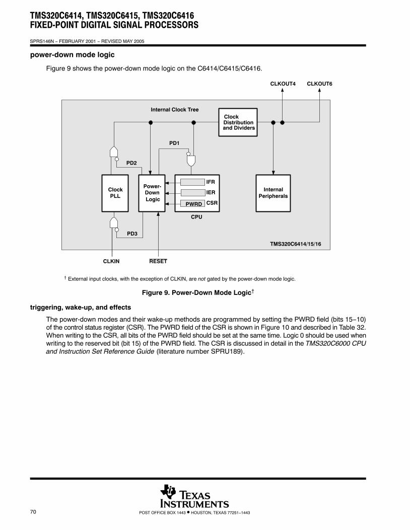
TMS320C6414, TMS320C6415, TMS320C6416FIXED-POINT DIGITAL SIGNAL PROCESSORS
SPRS146N − FEBRUARY 2001 − REVISED MAY 2005
70 POST OFFICE BOX 1443 • HOUSTON, TEXAS 77251−1443
power-down mode logic
Figure 9 shows the power-down mode logic on the C6414/C6415/C6416.
PWRD
Internal Clock Tree
CPU
IFR
IER
CSR
PD1
PD2
Power-DownLogic
ClockPLL
CLKIN RESET
CLKOUT6
PD3
InternalPeripherals
CLKOUT4
Clock
and DividersDistribution
† External input clocks, with the exception of CLKIN, are not gated by the power-down mode logic.
TMS320C6414/15/16
Figure 9. Power-Down Mode Logic†
triggering, wake-up, and effects
The power-down modes and their wake-up methods are programmed by setting the PWRD field (bits 15−10)of the control status register (CSR). The PWRD field of the CSR is shown in Figure 10 and described in Table 32.When writing to the CSR, all bits of the PWRD field should be set at the same time. Logic 0 should be used whenwriting to the reserved bit (bit 15) of the PWRD field. The CSR is discussed in detail in the TMS320C6000 CPUand Instruction Set Reference Guide (literature number SPRU189).
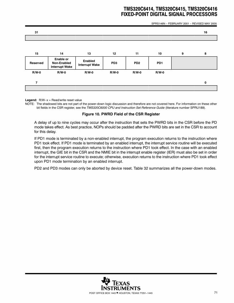
TMS320C6414, TMS320C6415, TMS320C6416FIXED-POINT DIGITAL SIGNAL PROCESSORS
SPRS146N − FEBRUARY 2001 − REVISED MAY 2005
71POST OFFICE BOX 1443 • HOUSTON, TEXAS 77251−1443
31 16
15 14 13 12 11 10 9 8
ReservedEnable or
Non-EnabledInterrupt Wake
EnabledInterrupt Wake PD3 PD2 PD1
R/W-0 R/W-0 R/W-0 R/W-0 R/W-0 R/W-0
7 0
Legend: R/W−x = Read/write reset valueNOTE: The shadowed bits are not part of the power-down logic discussion and therefore are not covered here. For information on these other
bit fields in the CSR register, see the TMS320C6000 CPU and Instruction Set Reference Guide (literature number SPRU189).
Figure 10. PWRD Field of the CSR Register
A delay of up to nine cycles may occur after the instruction that sets the PWRD bits in the CSR before the PDmode takes effect. As best practice, NOPs should be padded after the PWRD bits are set in the CSR to accountfor this delay.
If PD1 mode is terminated by a non-enabled interrupt, the program execution returns to the instruction wherePD1 took effect. If PD1 mode is terminated by an enabled interrupt, the interrupt service routine will be executedfirst, then the program execution returns to the instruction where PD1 took effect. In the case with an enabledinterrupt, the GIE bit in the CSR and the NMIE bit in the interrupt enable register (IER) must also be set in orderfor the interrupt service routine to execute; otherwise, execution returns to the instruction where PD1 took effectupon PD1 mode termination by an enabled interrupt.
PD2 and PD3 modes can only be aborted by device reset. Table 32 summarizes all the power-down modes.

TMS320C6414, TMS320C6415, TMS320C6416FIXED-POINT DIGITAL SIGNAL PROCESSORS
SPRS146N − FEBRUARY 2001 − REVISED MAY 2005
72 POST OFFICE BOX 1443 • HOUSTON, TEXAS 77251−1443
Table 32. Characteristics of the Power-Down Modes
PRWD FIELD(BITS 15−10)
POWER-DOWNMODE WAKE-UP METHOD EFFECT ON CHIP’S OPERATION
000000 No power-down — —
001001 PD1 Wake by an enabled interrupt CPU halted (except for the interrupt logic)Power-down mode blocks the internal clock inputs at the
010001 PD1Wake by an enabled ornon-enabled interrupt
Power down mode blocks the internal clock inputs at theboundary of the CPU, preventing most of the CPU’s logic fromswitching. During PD1, EDMA transactions can proceedbetween peripherals and internal memory.
011010 PD2† Wake by a device reset
Output clock from PLL is halted, stopping the internal clockstructure from switching and resulting in the entire chip beinghalted. All register and internal RAM contents are preserved. Allfunctional I/O “freeze” in the last state when the PLL clock isturned off.
011100 PD3† Wake by a device reset
Input clock to the PLL stops generating clocks. All register andinternal RAM contents are preserved. All functional I/O “freeze” inthe last state when the PLL clock is turned off. Following reset, thePLL needs time to re-lock, just as it does following power-up. Wake-up from PD3 takes longer than wake-up from PD2 becausethe PLL needs to be re-locked, just as it does following power-up.
All others Reserved — —† When entering PD2 and PD3, all functional I/O remains in the previous state. However, for peripherals which are asynchronous in nature or
peripherals with an external clock source, output signals may transition in response to stimulus on the inputs. Under these conditions,peripherals will not operate according to specifications.
C64x power-down mode with an emulator
If user power-down modes are programmed, and an emulator is attached, the modes will be masked to allowthe emulator access to the system. This condition prevails until the emulator is reset or the cable is removedfrom the header. If power measurements are to be performed when in a power-down mode, the emulator cableshould be removed.
When the DSP is in power-down mode PD2 or PD3, emulation logic will force any emulation executioncommand (such as Step or Run) to spin in IDLE. For this reason, PC writes (such as loading code) will fail. A DSPreset will be required to get the DSP out of PD2/PD3.
power-supply sequencing
TI DSPs do not require specific power sequencing between the core supply and the I/O supply. However,systems should be designed to ensure that neither supply is powered up for extended periods of time(>1 second) if the other supply is below the proper operating voltage.
power-supply design considerations
A dual-power supply with simultaneous sequencing can be used to eliminate the delay between core and I/Opower up. A Schottky diode can also be used to tie the core rail to the I/O rail (see Figure 11).

TMS320C6414, TMS320C6415, TMS320C6416FIXED-POINT DIGITAL SIGNAL PROCESSORS
SPRS146N − FEBRUARY 2001 − REVISED MAY 2005
73POST OFFICE BOX 1443 • HOUSTON, TEXAS 77251−1443
DVDD
CVDD
VSS
C6000DSP
SchottkyDiode
I/O Supply
Core Supply
GND
Figure 11. Schottky Diode Diagram
Core and I/O supply voltage regulators should be located close to the DSP (or DSP array) to minimizeinductance and resistance in the power delivery path. Additionally, when designing for high-performanceapplications utilizing the C6000™ platform of DSPs, the PC board should include separate power planes forcore, I/O, and ground, all bypassed with high-quality low-ESL/ESR capacitors.
power-supply decoupling
In order to properly decouple the supply planes from system noise, place as many capacitors (caps) as possibleclose to the DSP. Assuming 0603 caps, the user should be able to fit a total of 60 caps, 30 for the core supplyand 30 for the I/O supply. These caps need to be close to the DSP power pins, no more than 1.25 cm maximumdistance to be effective. Physically smaller caps, such as 0402, are better because of their lower parasiticinductance. Proper capacitance values are also important. Small bypass caps (near 560 pF) should be closestto the power pins. Medium bypass caps (220 nF or as large as can be obtained in a small package) should benext closest. TI recommends no less than 8 small and 8 medium caps per supply (32 total) be placedimmediately next to the BGA vias, using the “interior” BGA space and at least the corners of the “exterior”.
Eight larger caps (4 for each supply) can be placed further away for bulk decoupling. Large bulk caps (on theorder of 100 µF) should be furthest away (but still as close as possible). No less than 4 large caps per supply(8 total) should be placed outside of the BGA.
Any cap selection needs to be evaluated from a yield/manufacturing point-of-view. As with the selection of anycomponent, verification of capacitor availability over the product’s production lifetime should be considered.

TMS320C6414, TMS320C6415, TMS320C6416FIXED-POINT DIGITAL SIGNAL PROCESSORS
SPRS146N − FEBRUARY 2001 − REVISED MAY 2005
74 POST OFFICE BOX 1443 • HOUSTON, TEXAS 77251−1443
IEEE 1149.1 JTAG compatibility statement
The TMS320C6414/15/16 DSP requires that both TRST and RESET be asserted upon power up to be properlyinitialized. While RESET initializes the DSP core, TRST initializes the DSP’s emulation logic. Both resets arerequired for proper operation.
Note: TRST is synchronous and must be clocked by TCLK; otherwise, BSCAN may not respond as expectedafter TRST is asserted.
While both TRST and RESET need to be asserted upon power up, only RESET needs to be released for theDSP to boot properly. TRST may be asserted indefinitely for normal operation, keeping the JTAG port interfaceand DSP’s emulation logic in the reset state. TRST only needs to be released when it is necessary to use a JTAGcontroller to debug the DSP or exercise the DSP’s boundary scan functionality. RESET must be released inorder for boundary-scan JTAG to read the variant field of IDCODE correctly. Other boundary-scan instructionswork correctly independent of current state of RESET.
For maximum reliability, the TMS320C6414/15/16 DSP includes an internal pulldown (IPD) on the TRST pinto ensure that TRST will always be asserted upon power up and the DSP’s internal emulation logic will alwaysbe properly initialized. JTAG controllers from Texas Instruments actively drive TRST high. However, somethird-party JTAG controllers may not drive TRST high but expect the use of a pullup resistor on TRST. Whenusing this type of JTAG controller, assert TRST to intialize the DSP after powerup and externally drive TRSThigh before attempting any emulation or boundary scan operations.
Following the release of RESET, the low-to-high transition of TRST must occur to latch the state of EMU1 andEMU0. The EMU[1:0] pins configure the device for either Boundary Scan mode or Normal/Emulation mode. Formore detailed information, see the terminal functions section of this data sheet.
Note: The DESIGN_WARNING section of the TMS320C6414/15/16 BSDL file contains information andconstraints regarding proper device operation while in Boundary Scan Mode.
EMIF device speed
The rated EMIF speed, referring to both EMIFA and EMIFB, of these devices only applies to the SDRAMinterface when in a system that meets the following requirements:
− 1 chip-enable (CE) space (maximum of 2 chips) of SDRAM connected to EMIF
− up to 1 CE space of buffers connected to EMIF
− EMIF trace lengths between 1 and 3 inches
− 166-MHz SDRAM for 133-MHz operation (applies only to EMIFA)
− 143-MHz SDRAM for 100-MHz operation
Other configurations may be possible, but timing analysis must be done to verify all AC timings are met.Verification of AC timings is mandatory when using configurations other than those specified above. TIrecommends utilizing I/O buffer information specification (IBIS) to analyze all AC timings.
To properly use IBIS models to attain accurate timing analysis for a given system, see the Using IBIS Modelsfor Timing Analysis application report (literature number SPRA839).
To maintain signal integrity, serial termination resistors should be inserted into all EMIF output signal lines (seethe Terminal Functions table for the EMIF output signals).

TMS320C6414, TMS320C6415, TMS320C6416FIXED-POINT DIGITAL SIGNAL PROCESSORS
SPRS146N − FEBRUARY 2001 − REVISED MAY 2005
75POST OFFICE BOX 1443 • HOUSTON, TEXAS 77251−1443
bootmode
The C6414/15/16 device resets using the active-low signal RESET. While RESET is low, the device is held inreset and is initialized to the prescribed reset state. Refer to reset timing for reset timing characteristics andstates of device pins during reset. The release of RESET starts the processor running with the prescribed deviceconfiguration and boot mode.
The C6414/C6415/C6416 has three types of boot modes:
Host boot
If host boot is selected, upon release of RESET, the CPU is internally “stalled” while the remainder of thedevice is released. During this period, an external host can initialize the CPU’s memory space as necessarythrough the host interface, including internal configuration registers, such as those that control the EMIF orother peripherals. For the C6414 device, the HPI peripheral is used for host boot. For the C6415/C6416device, the HPI peripheral is used for host boot if PCI_EN = 0, and the PCI peripheral is used for host boot ifPCI_EN = 1. Once the host is finished with all necessary initialization, it must set the DSPINT bit in the HPICregister to complete the boot process. This transition causes the boot configuration logic to bring the CPUout of the “stalled” state. The CPU then begins execution from address 0. The DSPINT condition is notlatched by the CPU, because it occurs while the CPU is still internally “stalled”. Also, DSPINT brings the CPUout of the “stalled” state only if the host boot process is selected. All memory may be written to and read bythe host. This allows for the host to verify what it sends to the DSP if required. After the CPU is out of the“stalled” state, the CPU needs to clear the DSPINT, otherwise, no more DSPINTs can be received.
EMIF boot (using default ROM timings)
Upon the release of RESET, the 1K-Byte ROM code located in the beginning of CE1 is copied to address 0by the EDMA using the default ROM timings, while the CPU is internally “stalled”. The data should be storedin the endian format that the system is using. In this case, the EMIF automatically assembles consecutive8-bit bytes to form the 32-bit instruction words to be copied. The transfer is automatically done by the EDMAas a single-frame block transfer from the ROM to address 0. After completion of the block transfer, the CPUis released from the “stalled” state and starts running from address 0.
No boot
With no boot, the CPU begins direct execution from the memory located at address 0. Note: operation isundefined if invalid code is located at address 0.
reset
A hardware reset (RESET) is required to place the DSP into a known good state out of power-up. The RESETsignal can be asserted (pulled low) prior to ramping the core and I/O voltages or after the core and I/O voltageshave reached their proper operating conditions. As a best practice, reset should be held low during power-up.Prior to deasserting RESET (low-to-high transition), the core and I/O voltages should be at their properoperating conditions and CLKIN should also be running at the correct frequency.
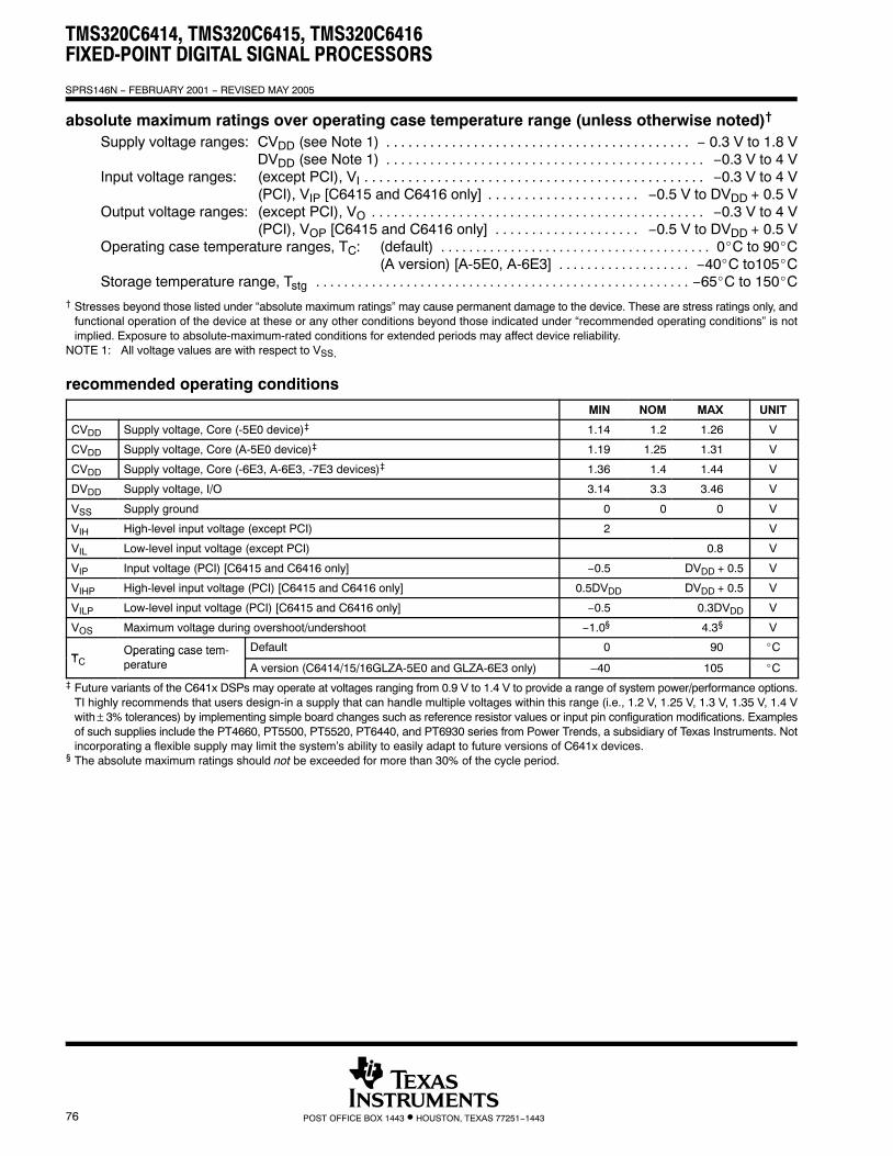
TMS320C6414, TMS320C6415, TMS320C6416FIXED-POINT DIGITAL SIGNAL PROCESSORS
SPRS146N − FEBRUARY 2001 − REVISED MAY 2005
76 POST OFFICE BOX 1443 • HOUSTON, TEXAS 77251−1443
absolute maximum ratings over operating case temperature range (unless otherwise noted)†
Supply voltage ranges: CVDD (see Note 1) − 0.3 V to 1.8 V. . . . . . . . . . . . . . . . . . . . . . . . . . . . . . . . . . . . . . . . . . DVDD (see Note 1) −0.3 V to 4 V. . . . . . . . . . . . . . . . . . . . . . . . . . . . . . . . . . . . . . . . . . . .
Input voltage ranges: (except PCI), VI −0.3 V to 4 V. . . . . . . . . . . . . . . . . . . . . . . . . . . . . . . . . . . . . . . . . . . . . . . (PCI), VIP [C6415 and C6416 only] −0.5 V to DVDD + 0.5 V. . . . . . . . . . . . . . . . . . . . .
Output voltage ranges: (except PCI), VO −0.3 V to 4 V. . . . . . . . . . . . . . . . . . . . . . . . . . . . . . . . . . . . . . . . . . . . . . (PCI), VOP [C6415 and C6416 only] −0.5 V to DVDD + 0.5 V. . . . . . . . . . . . . . . . . . . .
Operating case temperature ranges, TC: (default) 0C to 90C. . . . . . . . . . . . . . . . . . . . . . . . . . . . . . . . . . . . . . . (A version) [A-5E0, A-6E3] −40C to105C. . . . . . . . . . . . . . . . . . .
Storage temperature range, Tstg −65C to 150C. . . . . . . . . . . . . . . . . . . . . . . . . . . . . . . . . . . . . . . . . . . . . . . . . . . . . .
† Stresses beyond those listed under “absolute maximum ratings” may cause permanent damage to the device. These are stress ratings only, andfunctional operation of the device at these or any other conditions beyond those indicated under “recommended operating conditions” is notimplied. Exposure to absolute-maximum-rated conditions for extended periods may affect device reliability.
NOTE 1: All voltage values are with respect to VSS.
recommended operating conditions
MIN NOM MAX UNIT
CVDD Supply voltage, Core (-5E0 device)‡ 1.14 1.2 1.26 V
CVDD Supply voltage, Core (A-5E0 device)‡ 1.19 1.25 1.31 V
CVDD Supply voltage, Core (-6E3, A-6E3, -7E3 devices)‡ 1.36 1.4 1.44 V
DVDD Supply voltage, I/O 3.14 3.3 3.46 V
VSS Supply ground 0 0 0 V
VIH High-level input voltage (except PCI) 2 V
VIL Low-level input voltage (except PCI) 0.8 V
VIP Input voltage (PCI) [C6415 and C6416 only] −0.5 DVDD + 0.5 V
VIHP High-level input voltage (PCI) [C6415 and C6416 only] 0.5DVDD DVDD + 0.5 V
VILP Low-level input voltage (PCI) [C6415 and C6416 only] −0.5 0.3DVDD V
VOS Maximum voltage during overshoot/undershoot −1.0§ 4.3§ V
TOperating case tem- Default 0 90 C
TCOperating case temperature A version (C6414/15/16GLZA-5E0 and GLZA-6E3 only) –40 105 C
‡ Future variants of the C641x DSPs may operate at voltages ranging from 0.9 V to 1.4 V to provide a range of system power/performance options.TI highly recommends that users design-in a supply that can handle multiple voltages within this range (i.e., 1.2 V, 1.25 V, 1.3 V, 1.35 V, 1.4 Vwith ± 3% tolerances) by implementing simple board changes such as reference resistor values or input pin configuration modifications. Examplesof such supplies include the PT4660, PT5500, PT5520, PT6440, and PT6930 series from Power Trends, a subsidiary of Texas Instruments. Notincorporating a flexible supply may limit the system’s ability to easily adapt to future versions of C641x devices.
§ The absolute maximum ratings should not be exceeded for more than 30% of the cycle period.
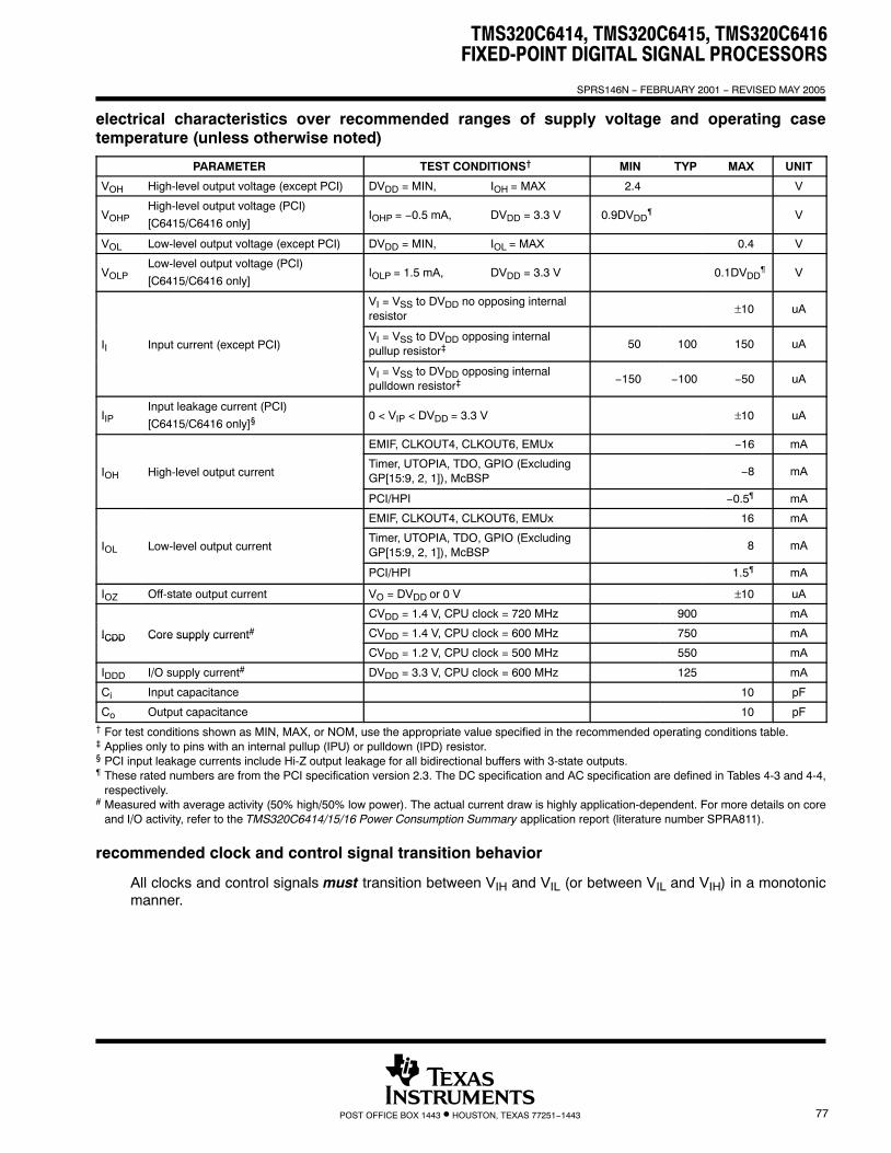
TMS320C6414, TMS320C6415, TMS320C6416FIXED-POINT DIGITAL SIGNAL PROCESSORS
SPRS146N − FEBRUARY 2001 − REVISED MAY 2005
77POST OFFICE BOX 1443 • HOUSTON, TEXAS 77251−1443
electrical characteristics over recommended ranges of supply voltage and operating casetemperature (unless otherwise noted)
PARAMETER TEST CONDITIONS† MIN TYP MAX UNIT
VOH High-level output voltage (except PCI) DVDD = MIN, IOH = MAX 2.4 V
VOHPHigh-level output voltage (PCI)
[C6415/C6416 only]IOHP = −0.5 mA, DVDD = 3.3 V 0.9DVDD
¶ V
VOL Low-level output voltage (except PCI) DVDD = MIN, IOL = MAX 0.4 V
VOLPLow-level output voltage (PCI)
[C6415/C6416 only]IOLP = 1.5 mA, DVDD = 3.3 V 0.1DVDD
¶ V
VI = VSS to DVDD no opposing internal resistor
±10 uA
II Input current (except PCI)VI = VSS to DVDD opposing internal pullup resistor‡
50 100 150 uA
VI = VSS to DVDD opposing internal pulldown resistor‡
−150 −100 −50 uA
IIPInput leakage current (PCI)
[C6415/C6416 only]§0 < VIP < DVDD = 3.3 V ±10 uA
EMIF, CLKOUT4, CLKOUT6, EMUx −16 mA
IOH High-level output currentTimer, UTOPIA, TDO, GPIO (ExcludingGP[15:9, 2, 1]), McBSP
−8 mA
PCI/HPI −0.5¶ mA
EMIF, CLKOUT4, CLKOUT6, EMUx 16 mA
IOL Low-level output currentTimer, UTOPIA, TDO, GPIO (ExcludingGP[15:9, 2, 1]), McBSP
8 mA
PCI/HPI 1.5¶ mA
IOZ Off-state output current VO = DVDD or 0 V ±10 uA
CVDD = 1.4 V, CPU clock = 720 MHz 900 mA
ICDD Core supply current# CVDD = 1.4 V, CPU clock = 600 MHz 750 mAICDD Core supply current
CVDD = 1.2 V, CPU clock = 500 MHz 550 mA
IDDD I/O supply current# DVDD = 3.3 V, CPU clock = 600 MHz 125 mA
Ci Input capacitance 10 pF
Co Output capacitance 10 pF† For test conditions shown as MIN, MAX, or NOM, use the appropriate value specified in the recommended operating conditions table.‡ Applies only to pins with an internal pullup (IPU) or pulldown (IPD) resistor.§ PCI input leakage currents include Hi-Z output leakage for all bidirectional buffers with 3-state outputs.¶ These rated numbers are from the PCI specification version 2.3. The DC specification and AC specification are defined in Tables 4-3 and 4-4,
respectively.# Measured with average activity (50% high/50% low power). The actual current draw is highly application-dependent. For more details on core
and I/O activity, refer to the TMS320C6414/15/16 Power Consumption Summary application report (literature number SPRA811).
recommended clock and control signal transition behavior
All clocks and control signals must transition between VIH and VIL (or between VIL and VIH) in a monotonicmanner.
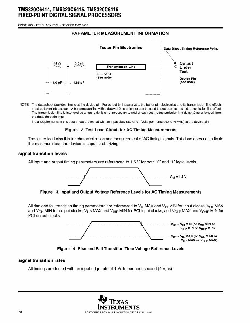
TMS320C6414, TMS320C6415, TMS320C6416FIXED-POINT DIGITAL SIGNAL PROCESSORS
SPRS146N − FEBRUARY 2001 − REVISED MAY 2005
78 POST OFFICE BOX 1443 • HOUSTON, TEXAS 77251−1443
PARAMETER MEASUREMENT INFORMATION
Transmission Line
4.0 pF 1.85 pF
Z0 = 50 (see note)
Tester Pin Electronics Data Sheet Timing Reference Point
OutputUnderTest
NOTE: The data sheet provides timing at the device pin. For output timing analysis, the tester pin electronics and its transmission line effectsmust be taken into account. A transmission line with a delay of 2 ns or longer can be used to produce the desired transmission line effect.The transmission line is intended as a load only. It is not necessary to add or subtract the transmission line delay (2 ns or longer) fromthe data sheet timings.
42 3.5 nH
Device Pin(see note)
Input requirements in this data sheet are tested with an input slew rate of < 4 Volts per nanosecond (4 V/ns) at the device pin.
Figure 12. Test Load Circuit for AC Timing Measurements
The tester load circuit is for characterization and measurement of AC timing signals. This load does not indicatethe maximum load the device is capable of driving.
signal transition levels
All input and output timing parameters are referenced to 1.5 V for both “0” and “1” logic levels.
Vref = 1.5 V
Figure 13. Input and Output Voltage Reference Levels for AC Timing Measurements
All rise and fall transition timing parameters are referenced to VIL MAX and VIH MIN for input clocks, VOL MAXand VOH MIN for output clocks, VILP MAX and VIHP MIN for PCI input clocks, and VOLP MAX and VOHP MIN forPCI output clocks.
Vref = VIL MAX (or VOL MAX or
Vref = VIH MIN (or VOH MIN or VIHP MIN or VOHP MIN)
VILP MAX or VOLP MAX)
Figure 14. Rise and Fall Transition Time Voltage Reference Levels
signal transition rates
All timings are tested with an input edge rate of 4 Volts per nanosecond (4 V/ns).

TMS320C6414, TMS320C6415, TMS320C6416FIXED-POINT DIGITAL SIGNAL PROCESSORS
SPRS146N − FEBRUARY 2001 − REVISED MAY 2005
79POST OFFICE BOX 1443 • HOUSTON, TEXAS 77251−1443
PARAMETER MEASUREMENT INFORMATION (CONTINUED)
timing parameters and board routing analysis
The timing parameter values specified in this data sheet do not include delays by board routings. As a goodboard design practice, such delays must always be taken into account. Timing values may be adjusted byincreasing/decreasing such delays. TI recommends utilizing the available I/O buffer information specification(IBIS) models to analyze the timing characteristics correctly. If needed, external logic hardware such as buffersmay be used to compensate any timing differences.
For inputs, timing is most impacted by the round-trip propagation delay from the DSP to the external device andfrom the external device to the DSP. This round-trip delay tends to negatively impact the input setup time margin,but also tends to improve the input hold time margins (see Table 33 and Figure 15).
Figure 15 represents a general transfer between the DSP and an external device. The figure also representsboard route delays and how they are perceived by the DSP and the external device.
Table 33. Board-Level Timings Example (see Figure 15)
NO. DESCRIPTION
1 Clock route delay
2 Minimum DSP hold time
3 Minimum DSP setup time
4 External device hold time requirement
5 External device setup time requirement
6 Control signal route delay
7 External device hold time
8 External device access time
9 DSP hold time requirement
10 DSP setup time requirement
11 Data route delay
1
23
45
6
78
1011
ECLKOUTx (Output from DSP)
ECLKOUTx (Input to External Device)
Control Signals† (Output from DSP)
Control Signals (Input to External Device)
Data Signals‡ (Output from External Device)
Data Signals‡ (Input to DSP)
9
† Control signals include data for Writes.
‡ Data signals are generated during Reads from an external device.
Figure 15. Board-Level Input/Output Timings

TMS320C6414, TMS320C6415, TMS320C6416FIXED-POINT DIGITAL SIGNAL PROCESSORS
SPRS146N − FEBRUARY 2001 − REVISED MAY 2005
80 POST OFFICE BOX 1443 • HOUSTON, TEXAS 77251−1443
INPUT AND OUTPUT CLOCKS
timing requirements for CLKIN for −5E0 devices†‡§ (see Figure 16)
NO
−5E0A−5E0
UNITNO.PLL MODE x12 PLL MODE x6 x1 (BYPASS)
UNIT
MIN MAX MIN MAX MIN MAX
1 tc(CLKIN) Cycle time, CLKIN 24 33.3 13.3 33.3 13.3 33.3 ns
2 tw(CLKINH) Pulse duration, CLKIN high 0.4C 0.4C 0.45C ns
3 tw(CLKINL) Pulse duration, CLKIN low 0.4C 0.4C 0.45C ns
4 tt(CLKIN) Transition time, CLKIN 5 5 1 ns
5 tJ(CLKIN) Period jitter, CLKIN 0.02C 0.02C 0.02C ns† The reference points for the rise and fall transitions are measured at VIL MAX and VIH MIN.‡ For more details on the PLL multiplier factors (x6, x12), see the Clock PLL section of this data sheet.§ C = CLKIN cycle time in ns. For example, when CLKIN frequency is 50 MHz, use C = 20 ns.
timing requirements for CLKIN for -6E3 devices†‡§ (see Figure 16)
−6E3, A−6E3
NO. PLL MODE x12 PLL MODE x6 x1 (BYPASS) UNITNO.
MIN MAX MIN MAX MIN MAX
UNIT
1 tc(CLKIN) Cycle time, CLKIN 20 33.3 13.3 33.3 13.3 33.3 ns
2 tw(CLKINH) Pulse duration, CLKIN high 0.4C 0.4C 0.45C ns
3 tw(CLKINL) Pulse duration, CLKIN low 0.4C 0.4C 0.45C ns
4 tt(CLKIN) Transition time, CLKIN 5 5 1 ns
5 tJ(CLKIN) Period jitter, CLKIN 0.02C 0.02C 0.02C ns† The reference points for the rise and fall transitions are measured at VIL MAX and VIH MIN.‡ For more details on the PLL multiplier factors (x6, x12), see the Clock PLL section of this data sheet.§ C = CLKIN cycle time in ns. For example, when CLKIN frequency is 50 MHz, use C = 20 ns.
timing requirements for CLKIN for -7E3 devices†‡§ (see Figure 16)
−7E3
NO. PLL MODE x12 PLL MODE x6 x1 (BYPASS) UNITNO.
MIN MAX MIN MAX MIN MAX
UNIT
1 tc(CLKIN) Cycle time, CLKIN 16.6 33.3 13.3 33.3 13.3 33.3 ns
2 tw(CLKINH) Pulse duration, CLKIN high 0.4C 0.4C 0.45C ns
3 tw(CLKINL) Pulse duration, CLKIN low 0.4C 0.4C 0.45C ns
4 tt(CLKIN) Transition time, CLKIN 5 5 1 ns
5 tJ(CLKIN) Period jitter, CLKIN 0.02C 0.02C 0.02C ns† The reference points for the rise and fall transitions are measured at VIL MAX and VIH MIN.‡ For more details on the PLL multiplier factors (x6, x12), see the Clock PLL section of this data sheet.§ C = CLKIN cycle time in ns. For example, when CLKIN frequency is 50 MHz, use C = 20 ns.
CLKIN
2
3
4
4
5 1
Figure 16. CLKIN Timing

TMS320C6414, TMS320C6415, TMS320C6416FIXED-POINT DIGITAL SIGNAL PROCESSORS
SPRS146N − FEBRUARY 2001 − REVISED MAY 2005
81POST OFFICE BOX 1443 • HOUSTON, TEXAS 77251−1443
INPUT AND OUTPUT CLOCKS (CONTINUED)
switching characteristics over recommended operating conditions for CLKOUT4†‡§
(see Figure 17)
NO. PARAMETER
−5E0, A−5E0,−6E3, A−6E3,
−7E3 UNITNO. PARAMETERCLKMODE = x1, x6, x12
UNIT
MIN MAX
1 tJ(CKO4) Period jitter, CLKOUT4 0 ±175 ps
2 tw(CKO4H) Pulse duration, CLKOUT4 high 2P − 0.7 2P + 0.7 ns
3 tw(CKO4L) Pulse duration, CLKOUT4 low 2P − 0.7 2P + 0.7 ns
4 tt(CKO4) Transition time, CLKOUT4 1 ns† The reference points for the rise and fall transitions are measured at VOL MAX and VOH MIN.‡ PH is the high period of CLKIN in ns and PL is the low period of CLKIN in ns.§ P = 1/CPU clock frequency in nanoseconds (ns)
CLKOUT4
3
4
4
21
Figure 17. CLKOUT4 Timing
switching characteristics over recommended operating conditions for CLKOUT6†‡§
(see Figure 18)
NO. PARAMETER
−5E0, A−5E0,−6E3, A−6E3,
−7E3 UNITNO. PARAMETERCLKMODE = x1, x6, x12
UNIT
MIN MAX
1 tJ(CKO6) Period jitter, CLKOUT6 0 ±175 ps
2 tw(CKO6H) Pulse duration, CLKOUT6 high 3P − 0.7 3P + 0.7 ns
3 tw(CKO6L) Pulse duration, CLKOUT6 low 3P − 0.7 3P + 0.7 ns
4 tt(CKO6) Transition time, CLKOUT6 1 ns† The reference points for the rise and fall transitions are measured at VOL MAX and VOH MIN.‡ PH is the high period of CLKIN in ns and PL is the low period of CLKIN in ns.§ P = 1/CPU clock frequency in nanoseconds (ns)
CLKOUT6
2
3
4
4
1
Figure 18. CLKOUT6 Timing

TMS320C6414, TMS320C6415, TMS320C6416FIXED-POINT DIGITAL SIGNAL PROCESSORS
SPRS146N − FEBRUARY 2001 − REVISED MAY 2005
82 POST OFFICE BOX 1443 • HOUSTON, TEXAS 77251−1443
INPUT AND OUTPUT CLOCKS (CONTINUED)
timing requirements for ECLKIN for EMIFA and EMIFB†‡§¶ (see Figure 19)
NO.
−5E0, A−5E0,−6E3, A−6E3,
−7E3 UNIT
MIN MAX
1 tc(EKI) Cycle time, ECLKIN 6# 16P ns
2 tw(EKIH) Pulse duration, ECLKIN high 2.7 ns
3 tw(EKIL) Pulse duration, ECLKIN low 2.7 ns
4 tt(EKI) Transition time, ECLKIN 2 ns
5 tJ(EKI) Period jitter, ECLKIN 0.02E ns† P = 1/CPU clock frequency in ns. For example, when running parts at 600 MHz, use P = 1.67 ns.‡ The reference points for the rise and fall transitions are measured at VIL MAX and VIH MIN.§ These C64x™ devices have two EMIFs (64-bit EMIFA and 16-bit EMIFB). All EMIFA signals are prefixed by an “A” and all EMIFB signals are
prefixed by a “B”. Throughout the rest of this document, in generic EMIF areas of discussion, the prefix “A” or “B” may be omitted.¶ E = the EMIF input clock (ECLKIN, CPU/4 clock, or CPU/6 clock) period in ns for EMIFA or EMIFB.# Minimum ECLKIN cycle times must be met, even when ECLKIN is generated by an internal clock source. Minimum ECLKIN times are based
on internal logic speed; the maximum useable speed of the EMIF may be lower due to AC timing requirements. On the 7E3 and 6E3 devices,133-MHz operation is achievable if the requirements of the EMIF Device Speed section are met. On the 5E0 devices, 100-MHz operation isachievable if the requirements of the EMIF Device Speed section are met.
ECLKIN
2
3
4
4
5 1
Figure 19. ECLKIN Timing for EMIFA and EMIFB
switching characteristics over recommended operating conditions for ECLKOUT1 for EMIFA andEMIFB modules§¶|| (see Figure 20)
NO. PARAMETER
−5E0, A−5E0,−6E3, A−6E3,
−7E3 UNIT
MIN MAX
1 tJ(EKO1) Period jitter, ECLKOUT1 0 ±175 ps
2 tw(EKO1H) Pulse duration, ECLKOUT1 high EH − 0.7 EH + 0.7 ns
3 tw(EKO1L) Pulse duration, ECLKOUT1 low EL − 0.7 EL + 0.7 ns
4 tt(EKO1) Transition time, ECLKOUT1 1 ns
5 td(EKIH-EKO1H) Delay time, ECLKIN high to ECLKOUT1 high 1 8 ns
6 td(EKIL-EKO1L) Delay time, ECLKIN low to ECLKOUT1 low 1 8 ns§ These C64x™ devices have two EMIFs (64-bit EMIFA and 16-bit EMIFB). All EMIFA signals are prefixed by an “A” and all EMIFB signals are
prefixed by a “B”. Throughout the rest of this document, in generic EMIF areas of discussion, the prefix “A” or “B” may be omitted.¶ E = the EMIF input clock (ECLKIN, CPU/4 clock, or CPU/6 clock) period in ns for EMIFA or EMIFB.|| The reference points for the rise and fall transitions are measured at VOL MAX and VOH MIN. EH is the high period of E (EMIF input clock period) in ns and EL is the low period of E (EMIF input clock period) in ns for EMIFA or EMIFB. This cycle-to-cycle jitter specification was measured with CPU/4 or CPU/6 as the source of the EMIF input clock.

TMS320C6414, TMS320C6415, TMS320C6416FIXED-POINT DIGITAL SIGNAL PROCESSORS
SPRS146N − FEBRUARY 2001 − REVISED MAY 2005
83POST OFFICE BOX 1443 • HOUSTON, TEXAS 77251−1443
INPUT AND OUTPUT CLOCKS (CONTINUED)
1
56
23
ECLKIN
ECLKOUT1
4 4
Figure 20. ECLKOUT1 Timing for EMIFA and EMIFB Modules
switching characteristics over recommended operating conditions for ECLKOUT2 for the EMIFAand EMIFB modules†‡§ (see Figure 21)
NO. PARAMETER
−5E0, A−5E0,−6E3, A−6E3,
−7E3 UNIT
MIN MAX
1 tJ(EKO2) Period jitter, ECLKOUT2 0 ±175¶ ps
2 tw(EKO2H) Pulse duration, ECLKOUT2 high 0.5NE − 0.7 0.5NE + 0.7 ns
3 tw(EKO2L) Pulse duration, ECLKOUT2 low 0.5NE − 0.7 0.5NE + 0.7 ns
4 tt(EKO2) Transition time, ECLKOUT2 1 ns
5 td(EKIH-EKO2H) Delay time, ECLKIN high to ECLKOUT2 high 1 8 ns
6 td(EKIH-EKO2L) Delay time, ECLKIN high to ECLKOUT2 low 1 8 ns† The reference points for the rise and fall transitions are measured at VOL MAX and VOH MIN.‡ These C64x™ devices have two EMIFs (64-bit EMIFA and 16-bit EMIFB). All EMIFA signals are prefixed by an “A” and all EMIFB signals are
prefixed by a “B”. Throughout the rest of this document, in generic EMIF areas of discussion, the prefix “A” or “B” may be omitted.§ E = the EMIF input clock (ECLKIN, CPU/4 clock, or CPU/6 clock) period in ns for EMIFA or EMIFB.
N = the EMIF input clock divider; N = 1, 2, or 4.¶ This cycle-to-cycle jitter specification was measured with CPU/4 or CPU/6 as the source of the EMIF input clock.
5 6
ECLKIN
ECLKOUT2
32 4 4
1
Figure 21. ECLKOUT2 Timing for the EMIFA and EMIFB Modules

TMS320C6414, TMS320C6415, TMS320C6416FIXED-POINT DIGITAL SIGNAL PROCESSORS
SPRS146N − FEBRUARY 2001 − REVISED MAY 2005
84 POST OFFICE BOX 1443 • HOUSTON, TEXAS 77251−1443
ASYNCHRONOUS MEMORY TIMING
timing requirements for asynchronous memory cycles for EMIFA module†‡§
(see Figure 22 and Figure 23)
NO.
−5E0−6E3−7E3
A−5E0A−6E3 UNIT
MIN MAX MIN MAX
3 tsu(EDV-AREH) Setup time, EDx valid before ARE high 6.5 6.5 ns
4 th(AREH-EDV) Hold time, EDx valid after ARE high 1 1 ns
6 tsu(ARDY-EKO1H) Setup time, ARDY valid before ECLKOUTx high 3 3 ns
7 th(EKO1H-ARDY) Hold time, ARDY valid after ECLKOUTx high
Rev 1.1 andearlier
1 1.5 ns7 th(EKO1H-ARDY) Hold time, ARDY valid after ECLKOUTx high
Rev 2.0 1.3 1.5 ns† To ensure data setup time, simply program the strobe width wide enough. ARDY is internally synchronized. The ARDY signal is only recognized
two cycles before the end of the programmed strobe time and while ARDY is low, the strobe time is extended cycle-by-cycle. When ARDY isrecognized low, the end of the strobe time is two cycles after ARDY is recognized high. To use ARDY as an asynchronous input, the pulse widthof the ARDY signal should be wide enough (e.g., pulse width = 2E) to ensure setup and hold time is met.
‡ RS = Read setup, RST = Read strobe, RH = Read hold, WS = Write setup, WST = Write strobe, WH = Write hold. These parameters areprogrammed via the EMIF CE space control registers.
§ These C64x™ devices have two EMIFs (EMIFA and EMIFB). All EMIFA signals are prefixed by an “A” and all EMIFB signals are prefixed by a“B”. Throughout the rest of this document, in generic EMIF areas of discussion, the prefix “A” or “B” may be omitted [e.g., the asynchronousmemory access signals are shown as generic (AOE, ARE, and AWE) instead of AAOE, AARE, and AAWE (for EMIFA) and BAOE, BARE, andBAWE (for EMIFB)].
switching characteristics over recommended operating conditions for asynchronous memorycycles for EMIFA moduleद# (see Figure 22 and Figure 23)
NO. PARAMETER
−5E0, A−5E0,−6E3, A−6E3,
−7E3 UNIT
MIN MAX
1 tosu(SELV-AREL) Output setup time, select signals valid to ARE low RS * E − 1.5 ns
2 toh(AREH-SELIV) Output hold time, ARE high to select signals invalid RH * E − 1.9 ns
5 td(EKO1H-AREV) Delay time, ECLKOUTx high to ARE valid 1 7 ns
8 tosu(SELV-AWEL) Output setup time, select signals valid to AWE low WS * E − 1.7 ns
9 toh(AWEH-SELIV) Output hold time, AWE high to select signals invalid WH * E − 1.8 ns
10 td(EKO1H-AWEV) Delay time, ECLKOUTx high to AWE valid 1.3 7.1 ns‡ RS = Read setup, RST = Read strobe, RH = Read hold, WS = Write setup, WST = Write strobe, WH = Write hold. These parameters are
programmed via the EMIF CE space control registers.§ These C64x™ devices have two EMIFs (EMIFA and EMIFB). All EMIFA signals are prefixed by an “A” and all EMIFB signals are prefixed by a
“B”. Throughout the rest of this document, in generic EMIF areas of discussion, the prefix “A” or “B” may be omitted [e.g., the asynchronousmemory access signals are shown as generic (AOE, ARE, and AWE) instead of AAOE, AARE, and AAWE (for EMIFA) and BAOE, BARE, andBAWE (for EMIFB)].
¶ E = ECLKOUT1 period in ns for EMIFA or EMIFB# Select signals for EMIFA include: ACEx, ABE[7:0], AEA[22:3], AAOE; and for EMIFA writes, include AED[63:0].
Select signals EMIFB include: BCEx, BBE[1:0], BEA[20:1], BAOE; and for EMIFB writes, include BED[15:0].
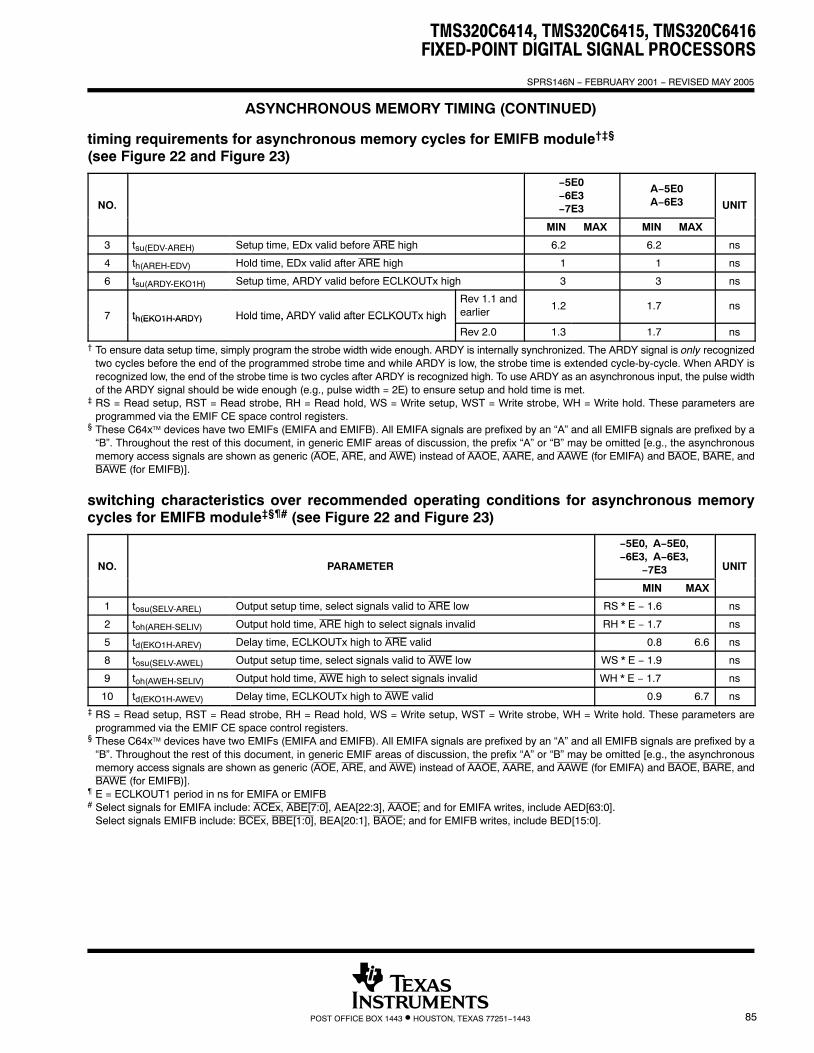
TMS320C6414, TMS320C6415, TMS320C6416FIXED-POINT DIGITAL SIGNAL PROCESSORS
SPRS146N − FEBRUARY 2001 − REVISED MAY 2005
85POST OFFICE BOX 1443 • HOUSTON, TEXAS 77251−1443
ASYNCHRONOUS MEMORY TIMING (CONTINUED)
timing requirements for asynchronous memory cycles for EMIFB module†‡§
(see Figure 22 and Figure 23)
NO.
−5E0−6E3−7E3
A−5E0A−6E3 UNIT
MIN MAX MIN MAX
3 tsu(EDV-AREH) Setup time, EDx valid before ARE high 6.2 6.2 ns
4 th(AREH-EDV) Hold time, EDx valid after ARE high 1 1 ns
6 tsu(ARDY-EKO1H) Setup time, ARDY valid before ECLKOUTx high 3 3 ns
7 th(EKO1H-ARDY) Hold time, ARDY valid after ECLKOUTx high
Rev 1.1 andearlier
1.2 1.7 ns7 th(EKO1H-ARDY) Hold time, ARDY valid after ECLKOUTx high
Rev 2.0 1.3 1.7 ns† To ensure data setup time, simply program the strobe width wide enough. ARDY is internally synchronized. The ARDY signal is only recognized
two cycles before the end of the programmed strobe time and while ARDY is low, the strobe time is extended cycle-by-cycle. When ARDY isrecognized low, the end of the strobe time is two cycles after ARDY is recognized high. To use ARDY as an asynchronous input, the pulse widthof the ARDY signal should be wide enough (e.g., pulse width = 2E) to ensure setup and hold time is met.
‡ RS = Read setup, RST = Read strobe, RH = Read hold, WS = Write setup, WST = Write strobe, WH = Write hold. These parameters areprogrammed via the EMIF CE space control registers.
§ These C64x™ devices have two EMIFs (EMIFA and EMIFB). All EMIFA signals are prefixed by an “A” and all EMIFB signals are prefixed by a“B”. Throughout the rest of this document, in generic EMIF areas of discussion, the prefix “A” or “B” may be omitted [e.g., the asynchronousmemory access signals are shown as generic (AOE, ARE, and AWE) instead of AAOE, AARE, and AAWE (for EMIFA) and BAOE, BARE, andBAWE (for EMIFB)].
switching characteristics over recommended operating conditions for asynchronous memorycycles for EMIFB moduleद# (see Figure 22 and Figure 23)
NO. PARAMETER
−5E0, A−5E0,−6E3, A−6E3,
−7E3 UNIT
MIN MAX
1 tosu(SELV-AREL) Output setup time, select signals valid to ARE low RS * E − 1.6 ns
2 toh(AREH-SELIV) Output hold time, ARE high to select signals invalid RH * E − 1.7 ns
5 td(EKO1H-AREV) Delay time, ECLKOUTx high to ARE valid 0.8 6.6 ns
8 tosu(SELV-AWEL) Output setup time, select signals valid to AWE low WS * E − 1.9 ns
9 toh(AWEH-SELIV) Output hold time, AWE high to select signals invalid WH * E − 1.7 ns
10 td(EKO1H-AWEV) Delay time, ECLKOUTx high to AWE valid 0.9 6.7 ns‡ RS = Read setup, RST = Read strobe, RH = Read hold, WS = Write setup, WST = Write strobe, WH = Write hold. These parameters are
programmed via the EMIF CE space control registers.§ These C64x™ devices have two EMIFs (EMIFA and EMIFB). All EMIFA signals are prefixed by an “A” and all EMIFB signals are prefixed by a
“B”. Throughout the rest of this document, in generic EMIF areas of discussion, the prefix “A” or “B” may be omitted [e.g., the asynchronousmemory access signals are shown as generic (AOE, ARE, and AWE) instead of AAOE, AARE, and AAWE (for EMIFA) and BAOE, BARE, andBAWE (for EMIFB)].
¶ E = ECLKOUT1 period in ns for EMIFA or EMIFB# Select signals for EMIFA include: ACEx, ABE[7:0], AEA[22:3], AAOE; and for EMIFA writes, include AED[63:0].
Select signals EMIFB include: BCEx, BBE[1:0], BEA[20:1], BAOE; and for EMIFB writes, include BED[15:0].
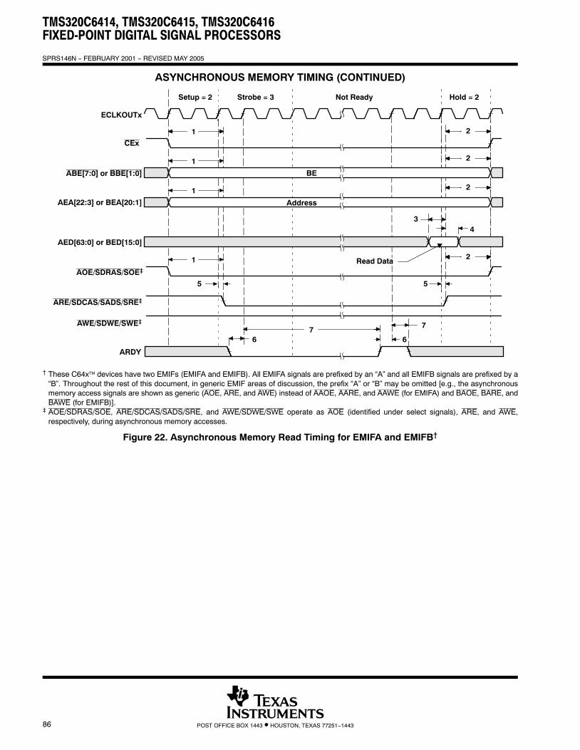
TMS320C6414, TMS320C6415, TMS320C6416FIXED-POINT DIGITAL SIGNAL PROCESSORS
SPRS146N − FEBRUARY 2001 − REVISED MAY 2005
86 POST OFFICE BOX 1443 • HOUSTON, TEXAS 77251−1443
ASYNCHRONOUS MEMORY TIMING (CONTINUED)
77
66
Setup = 2 Strobe = 3 Not Ready Hold = 2
BE
Address
1
1
1
1
5
4
5
2
2
2
2
3
Read Data
ARDY
ECLKOUTx
CEx
AEA[22:3] or BEA[20:1]
AED[63:0] or BED[15:0]
AOE/SDRAS/SOE‡
ARE/SDCAS/SADS/SRE‡
ABE[7:0] or BBE[1:0]
AWE/SDWE/SWE‡
† These C64x™ devices have two EMIFs (EMIFA and EMIFB). All EMIFA signals are prefixed by an “A” and all EMIFB signals are prefixed by a“B”. Throughout the rest of this document, in generic EMIF areas of discussion, the prefix “A” or “B” may be omitted [e.g., the asynchronousmemory access signals are shown as generic (AOE, ARE, and AWE) instead of AAOE, AARE, and AAWE (for EMIFA) and BAOE, BARE, andBAWE (for EMIFB)].
‡ AOE/SDRAS/SOE, ARE/SDCAS/SADS/SRE, and AWE/SDWE/SWE operate as AOE (identified under select signals), ARE, and AWE,respectively, during asynchronous memory accesses.
Figure 22. Asynchronous Memory Read Timing for EMIFA and EMIFB†
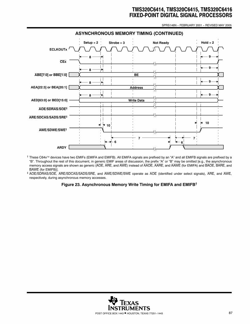
TMS320C6414, TMS320C6415, TMS320C6416FIXED-POINT DIGITAL SIGNAL PROCESSORS
SPRS146N − FEBRUARY 2001 − REVISED MAY 2005
87POST OFFICE BOX 1443 • HOUSTON, TEXAS 77251−1443
ASYNCHRONOUS MEMORY TIMING (CONTINUED)
Setup = 2 Strobe = 3 Not Ready Hold = 2
BE
Address
Write Data
1010
8
8
8
8
7766
9
9
9
9
ECLKOUTx
CEx
AEA[22:3] or BEA[20:1]
AED[63:0] or BED[15:0]
ABE[7:0] or BBE[1:0]
ARDY
AOE/SDRAS/SOE‡
ARE/SDCAS/SADS/SRE‡
AWE/SDWE/SWE‡
† These C64x™ devices have two EMIFs (EMIFA and EMIFB). All EMIFA signals are prefixed by an “A” and all EMIFB signals are prefixed by a“B”. Throughout the rest of this document, in generic EMIF areas of discussion, the prefix “A” or “B” may be omitted [e.g., the asynchronousmemory access signals are shown as generic (AOE, ARE, and AWE) instead of AAOE, AARE, and AAWE (for EMIFA) and BAOE, BARE, andBAWE (for EMIFB)].
‡ AOE/SDRAS/SOE, ARE/SDCAS/SADS/SRE, and AWE/SDWE/SWE operate as AOE (identified under select signals), ARE, and AWE,respectively, during asynchronous memory accesses.
Figure 23. Asynchronous Memory Write Timing for EMIFA and EMIFB†

TMS320C6414, TMS320C6415, TMS320C6416FIXED-POINT DIGITAL SIGNAL PROCESSORS
SPRS146N − FEBRUARY 2001 − REVISED MAY 2005
88 POST OFFICE BOX 1443 • HOUSTON, TEXAS 77251−1443
PROGRAMMABLE SYNCHRONOUS INTERFACE TIMING
timing requirements for programmable synchronous interface cycles for EMIFA module† (see Figure 24)
NO.
−5E0A−5E0
−6E3A−6E3−7E3 UNIT
MIN MAX MIN MAX
6 tsu(EDV-EKOxH) Setup time, read EDx valid before ECLKOUTx high 3.1 2 ns
7 th(EKOxH-EDV) Hold time, read EDx valid after ECLKOUTx high 1.5 1.5 ns† These C64x™ devices have two EMIFs (EMIFA and EMIFB). All EMIFA signals are prefixed by an “A” and all EMIFB signals are prefixed by a
“B”. Throughout the rest of this document, in generic EMIF areas of discussion, the prefix “A” or “B” may be omitted [e.g., the programmablesynchronous interface access signals are shown as generic (SADS/SRE, SOE, and SWE) instead of ASADS/ASRE, ASOE, and ASWE (forEMIFA) and BSADS/BSRE, BSOE, and BSWE (for EMIFB)].
switching characteristics over recommended operating conditions for programmablesynchronous interface cycles for EMIFA module†‡ (see Figure 24−Figure 26)
NO. PARAMETER
−5E0A−5E0
−6E3A−6E3−7E3 UNIT
MIN MAX MIN MAX
1 td(EKOxH-CEV) Delay time, ECLKOUTx high to CEx valid 1.3 6.4 1.3 4.9 ns
2 td(EKOxH-BEV) Delay time, ECLKOUTx high to BEx valid 6.4 4.9 ns
3 td(EKOxH-BEIV) Delay time, ECLKOUTx high to BEx invalid 1.3 1.3 ns
4 td(EKOxH-EAV) Delay time, ECLKOUTx high to EAx valid 6.4 4.9 ns
5 td(EKOxH-EAIV) Delay time, ECLKOUTx high to EAx invalid 1.3 1.3 ns
8 td(EKOxH-ADSV) Delay time, ECLKOUTx high to SADS/SRE valid 1.3 6.4 1.3 4.9 ns
9 td(EKOxH-OEV) Delay time, ECLKOUTx high to, SOE valid 1.3 6.4 1.3 4.9 ns
10 td(EKOxH-EDV) Delay time, ECLKOUTx high to EDx valid 6.4 4.9 ns
11 td(EKOxH-EDIV) Delay time, ECLKOUTx high to EDx invalid 1.3 1.3 ns
12 td(EKOxH-WEV) Delay time, ECLKOUTx high to SWE valid 1.3 6.4 1.3 4.9 ns† These C64x™ devices have two EMIFs (EMIFA and EMIFB). All EMIFA signals are prefixed by an “A” and all EMIFB signals are prefixed by a
“B”. Throughout the rest of this document, in generic EMIF areas of discussion, the prefix “A” or “B” may be omitted [e.g., the programmablesynchronous interface access signals are shown as generic (SADS/SRE, SOE, and SWE) instead of ASADS/ASRE, ASOE, and ASWE (forEMIFA) and BSADS/BSRE, BSOE, and BSWE (for EMIFB)].
‡ The following parameters are programmable via the EMIF CE Space Secondary Control register (CExSEC):− Read latency (SYNCRL): 0-, 1-, 2-, or 3-cycle read latency− Write latency (SYNCWL): 0-, 1-, 2-, or 3-cycle write latency− CEx assertion length (CEEXT): For standard SBSRAM or ZBT SRAM interface, CEx goes inactive after the final command has been issued
(CEEXT = 0). For synchronous FIFO interface with glue, CEx is active when SOE is active (CEEXT = 1).− Function of SADS/SRE (RENEN): For standard SBSRAM or ZBT SRAM interface, SADS/SRE acts as SADS with deselect cycles
(RENEN = 0). For FIFO interface, SADS/SRE acts as SRE with NO deselect cycles (RENEN = 1).− Synchronization clock (SNCCLK): Synchronized to ECLKOUT1 or ECLKOUT2

TMS320C6414, TMS320C6415, TMS320C6416FIXED-POINT DIGITAL SIGNAL PROCESSORS
SPRS146N − FEBRUARY 2001 − REVISED MAY 2005
89POST OFFICE BOX 1443 • HOUSTON, TEXAS 77251−1443
PROGRAMMABLE SYNCHRONOUS INTERFACE TIMING (CONTINUED)
timing requirements for programmable synchronous interface cycles for EMIFB module† (see Figure 24)
NO.
−5E0A−5E0
−6E3A−6E3−7E3 UNIT
MIN MAX MIN MAX
6 tsu(EDV-EKOxH) Setup time, read EDx valid before ECLKOUTx high 3.1 3.1 ns
7 th(EKOxH-EDV) Hold time, read EDx valid after ECLKOUTx high 1.5 1.5 ns† These C64x™ devices have two EMIFs (EMIFA and EMIFB). All EMIFA signals are prefixed by an “A” and all EMIFB signals are prefixed by a
“B”. Throughout the rest of this document, in generic EMIF areas of discussion, the prefix “A” or “B” may be omitted [e.g., the programmablesynchronous interface access signals are shown as generic (SADS/SRE, SOE, and SWE) instead of ASADS/ASRE, ASOE, and ASWE (forEMIFA) and BSADS/BSRE, BSOE, and BSWE (for EMIFB)].
switching characteristics over recommended operating conditions for programmablesynchronous interface cycles for EMIFB module†‡ (see Figure 24−Figure 26)
NO. PARAMETER
−5E0A−5E0
−6E3A−6E3−7E3 UNIT
MIN MAX MIN MAX
1 td(EKOxH-CEV) Delay time, ECLKOUTx high to CEx valid 1.3 6.4 1.3 6.4 ns
2 td(EKOxH-BEV) Delay time, ECLKOUTx high to BEx valid 6.4 6.4 ns
3 td(EKOxH-BEIV) Delay time, ECLKOUTx high to BEx invalid 1.3 1.3 ns
4 td(EKOxH-EAV) Delay time, ECLKOUTx high to EAx valid 6.4 6.4 ns
5 td(EKOxH-EAIV) Delay time, ECLKOUTx high to EAx invalid 1.3 1.3 ns
8 td(EKOxH-ADSV) Delay time, ECLKOUTx high to SADS/SRE valid 1.3 6.4 1.3 6.4 ns
9 td(EKOxH-OEV) Delay time, ECLKOUTx high to, SOE valid 1.3 6.4 1.3 6.4 ns
10 td(EKOxH-EDV) Delay time, ECLKOUTx high to EDx valid 6.4 6.4 ns
11 td(EKOxH-EDIV) Delay time, ECLKOUTx high to EDx invalid 1.3 1.3 ns
12 td(EKOxH-WEV) Delay time, ECLKOUTx high to SWE valid 1.3 6.4 1.3 6.4 ns† These C64x™ devices have two EMIFs (EMIFA and EMIFB). All EMIFA signals are prefixed by an “A” and all EMIFB signals are prefixed by a
“B”. Throughout the rest of this document, in generic EMIF areas of discussion, the prefix “A” or “B” may be omitted [e.g., the programmablesynchronous interface access signals are shown as generic (SADS/SRE, SOE, and SWE) instead of ASADS/ASRE, ASOE, and ASWE (forEMIFA) and BSADS/BSRE, BSOE, and BSWE (for EMIFB)].
‡ The following parameters are programmable via the EMIF CE Space Secondary Control register (CExSEC):− Read latency (SYNCRL): 0-, 1-, 2-, or 3-cycle read latency− Write latency (SYNCWL): 0-, 1-, 2-, or 3-cycle write latency− CEx assertion length (CEEXT): For standard SBSRAM or ZBT SRAM interface, CEx goes inactive after the final command has been issued
(CEEXT = 0). For synchronous FIFO interface with glue, CEx is active when SOE is active (CEEXT = 1).− Function of SADS/SRE (RENEN): For standard SBSRAM or ZBT SRAM interface, SADS/SRE acts as SADS with deselect cycles
(RENEN = 0). For FIFO interface, SADS/SRE acts as SRE with NO deselect cycles (RENEN = 1).− Synchronization clock (SNCCLK): Synchronized to ECLKOUT1 or ECLKOUT2

TMS320C6414, TMS320C6415, TMS320C6416FIXED-POINT DIGITAL SIGNAL PROCESSORS
SPRS146N − FEBRUARY 2001 − REVISED MAY 2005
90 POST OFFICE BOX 1443 • HOUSTON, TEXAS 77251−1443
PROGRAMMABLE SYNCHRONOUS INTERFACE TIMING (CONTINUED)
ECLKOUTx
CEx
ABE[7:0] or BBE[1:0]
AEA[22:3] or BEA[20:1]
AED[63:0] or BED[15:0]
ARE/SDCAS/SADS/SRE§
AOE/SDRAS/SOE§
AWE/SDWE/SWE§
BE1 BE2 BE3 BE4
Q1 Q2 Q3 Q4
9
1
4 5
8
9
67
3
1
2BE1 BE2 BE3 BE4
EA1 EA2 EA4
8
READ latency = 2
EA3
† These C64x™ devices have two EMIFs (EMIFA and EMIFB). All EMIFA signals are prefixed by an “A” and all EMIFB signals are prefixed by a“B”. Throughout the rest of this document, in generic EMIF areas of discussion, the prefix “A” or “B” may be omitted [e.g., the programmablesynchronous interface access signals are shown as generic (SADS/SRE, SOE, and SWE) instead of ASADS/ASRE, ASOE, and ASWE (forEMIFA) and BSADS/BSRE, BSOE, and BSWE (for EMIFB)].
‡ The read latency and the length of CEx assertion are programmable via the SYNCRL and CEEXT fields, respectively, in the EMIFx CE SpaceSecondary Control register (CExSEC). In this figure, SYNCRL = 2 and CEEXT = 0.
§ The following parameters are programmable via the EMIF CE Space Secondary Control register (CExSEC):− Read latency (SYNCRL): 0-, 1-, 2-, or 3-cycle read latency− Write latency (SYNCWL): 0-, 1-, 2-, or 3-cycle write latency− CEx assertion length (CEEXT): For standard SBSRAM or ZBT SRAM interface, CEx goes inactive after the final command has been issued
(CEEXT = 0). For synchronous FIFO interface with glue, CEx is active when SOE is active (CEEXT = 1).− Function of SADS/SRE (RENEN): For standard SBSRAM or ZBT SRAM interface, SADS/SRE acts as SADS with deselect cycles
(RENEN = 0). For FIFO interface, SADS/SRE acts as SRE with NO deselect cycles (RENEN = 1).− Synchronization clock (SNCCLK): Synchronized to ECLKOUT1 or ECLKOUT2
¶ ARE/SDCAS/SADS/SRE, AOE/SDRAS/SOE, and AWE/SDWE/SWE operate as SADS/SRE, SOE, and SWE, respectively, duringprogrammable synchronous interface accesses.
Figure 24. Programmable Synchronous Interface Read Timing for EMIFA and EMIFB(With Read Latency = 2)†‡§

TMS320C6414, TMS320C6415, TMS320C6416FIXED-POINT DIGITAL SIGNAL PROCESSORS
SPRS146N − FEBRUARY 2001 − REVISED MAY 2005
91POST OFFICE BOX 1443 • HOUSTON, TEXAS 77251−1443
PROGRAMMABLE SYNCHRONOUS INTERFACE TIMING (CONTINUED)
ECLKOUTx
CEx
ABE[7:0] or BBE[1:0]
AEA[22:3] or BEA[20:1]
AED[63:0] or BED[15:0]
ARE/SDCAS/SADS/SRE¶
AOE/SDRAS/SOE¶
AWE/SDWE/SWE¶
BE1 BE2 BE3 BE4
Q1 Q2 Q3 Q4
12
11
3
1
12
10
4
2
1
8
5
8
EA1 EA2 EA3 EA410
† These C64x™ devices have two EMIFs (EMIFA and EMIFB). All EMIFA signals are prefixed by an “A” and all EMIFB signals are prefixed by a“B”. Throughout the rest of this document, in generic EMIF areas of discussion, the prefix “A” or “B” may be omitted [e.g., the programmablesynchronous interface access signals are shown as generic (SADS/SRE, SOE, and SWE) instead of ASADS/ASRE, ASOE, and ASWE (forEMIFA) and BSADS/BSRE, BSOE, and BSWE (for EMIFB)].
‡ The write latency and the length of CEx assertion are programmable via the SYNCWL and CEEXT fields, respectively, in the EMIFx CE SpaceSecondary Control register (CExSEC). In this figure, SYNCWL = 0 and CEEXT = 0.
§ The following parameters are programmable via the EMIF CE Space Secondary Control register (CExSEC):− Read latency (SYNCRL): 0-, 1-, 2-, or 3-cycle read latency− Write latency (SYNCWL): 0-, 1-, 2-, or 3-cycle write latency− CEx assertion length (CEEXT): For standard SBSRAM or ZBT SRAM interface, CEx goes inactive after the final command has been issued
(CEEXT = 0). For synchronous FIFO interface with glue, CEx is active when SOE is active (CEEXT = 1).− Function of SADS/SRE (RENEN): For standard SBSRAM or ZBT SRAM interface, SADS/SRE acts as SADS with deselect cycles
(RENEN = 0). For FIFO interface, SADS/SRE acts as SRE with NO deselect cycles (RENEN = 1).− Synchronization clock (SNCCLK): Synchronized to ECLKOUT1 or ECLKOUT2
¶ ARE/SDCAS/SADS/SRE, AOE/SDRAS/SOE, and AWE/SDWE/SWE operate as SADS/SRE, SOE, and SWE, respectively, duringprogrammable synchronous interface accesses.
Figure 25. Programmable Synchronous Interface Write Timing for EMIFA and EMIFB(With Write Latency = 0)†‡§

TMS320C6414, TMS320C6415, TMS320C6416FIXED-POINT DIGITAL SIGNAL PROCESSORS
SPRS146N − FEBRUARY 2001 − REVISED MAY 2005
92 POST OFFICE BOX 1443 • HOUSTON, TEXAS 77251−1443
PROGRAMMABLE SYNCHRONOUS INTERFACE TIMING (CONTINUED)
ECLKOUTx
CEx
ABE[7:0] or BBE[1:0]
AEA[22:3] or BEA[20:1]
AED[63:0] or BED[15:0]
ARE/SDCAS/SADS/SRE¶
AOE/SDRAS/SOE¶
AWE/SDWE/SWE¶
BE1 BE2 BE3 BE4
Q1 Q2 Q311
3
12
10
4
2
1
8
5
8
EA1 EA2 EA3 EA410
WriteLatency =
1‡
1
Q4
12
† These C64x™ devices have two EMIFs (EMIFA and EMIFB). All EMIFA signals are prefixed by an “A” and all EMIFB signals are prefixed by a“B”. Throughout the rest of this document, in generic EMIF areas of discussion, the prefix “A” or “B” may be omitted [e.g., the programmablesynchronous interface access signals are shown as generic (SADS/SRE, SOE, and SWE) instead of ASADS/ASRE, ASOE, and ASWE (forEMIFA) and BSADS/BSRE, BSOE, and BSWE (for EMIFB)].
‡ The write latency and the length of CEx assertion are programmable via the SYNCWL and CEEXT fields, respectively, in the EMIFx CE SpaceSecondary Control register (CExSEC). In this figure, SYNCWL = 1 and CEEXT = 0.
§ The following parameters are programmable via the EMIF CE Space Secondary Control register (CExSEC):− Read latency (SYNCRL): 0-, 1-, 2-, or 3-cycle read latency− Write latency (SYNCWL): 0-, 1-, 2-, or 3-cycle write latency− CEx assertion length (CEEXT): For standard SBSRAM or ZBT SRAM interface, CEx goes inactive after the final command has been issued
(CEEXT = 0). For synchronous FIFO interface with glue, CEx is active when SOE is active (CEEXT = 1).− Function of SADS/SRE (RENEN): For standard SBSRAM or ZBT SRAM interface, SADS/SRE acts as SADS with deselect cycles
(RENEN = 0). For FIFO interface, SADS/SRE acts as SRE with NO deselect cycles (RENEN = 1).− Synchronization clock (SNCCLK): Synchronized to ECLKOUT1 or ECLKOUT2
¶ ARE/SDCAS/SADS/SRE, AOE/SDRAS/SOE, and AWE/SDWE/SWE operate as SADS/SRE, SOE, and SWE, respectively, duringprogrammable synchronous interface accesses.
Figure 26. Programmable Synchronous Interface Write Timing for EMIFA and EMIFB(With Write Latency = 1)†‡§

TMS320C6414, TMS320C6415, TMS320C6416FIXED-POINT DIGITAL SIGNAL PROCESSORS
SPRS146N − FEBRUARY 2001 − REVISED MAY 2005
93POST OFFICE BOX 1443 • HOUSTON, TEXAS 77251−1443
SYNCHRONOUS DRAM TIMING
timing requirements for synchronous DRAM cycles for EMIFA module† (see Figure 27)
NO.
−5E0A−5E0
−6E3A−6E3−7E3 UNIT
MIN MAX MIN MAX
6 tsu(EDV-EKO1H) Setup time, read EDx valid before ECLKOUTx high 2.1 0.6 ns
7 th(EKO1H-EDV) Hold time, read EDx valid after ECLKOUTx high 2.5 1.8 ns† These C64x™ devices have two EMIFs (EMIFA and EMIFB). All EMIFA signals are prefixed by an “A” and all EMIFB signals are prefixed by a
“B”. Throughout the rest of this document, in generic EMIF areas of discussion, the prefix “A” or “B” may be omitted [e.g., the synchronous DRAMmemory access signals are shown as generic ( SDCAS, SDWE, and SDRAS ) instead of ASDCAS, ASDWE, and ASDRAS (for EMIFA) andBSDCAS, BSDWE, and BSDRAS (for EMIFB)].
switching characteristics over recommended operating conditions for synchronous DRAM cyclesfor EMIFA module† (see Figure 27−Figure 34)
NO. PARAMETER
−5E0A−5E0
−6E3A−6E3−7E3 UNIT
MIN MAX MIN MAX
1 td(EKO1H-CEV) Delay time, ECLKOUTx high to CEx valid 1.3 6.4 1.3 4.9 ns
2 td(EKO1H-BEV) Delay time, ECLKOUTx high to BEx valid 6.4 4.9 ns
3 td(EKO1H-BEIV) Delay time, ECLKOUTx high to BEx invalid 1.3 1.3 ns
4 td(EKO1H-EAV) Delay time, ECLKOUTx high to EAx valid 6.4 4.9 ns
5 td(EKO1H-EAIV) Delay time, ECLKOUTx high to EAx invalid 1.3 1.3 ns
8 td(EKO1H-CASV) Delay time, ECLKOUTx high to SDCAS valid 1.3 6.4 1.3 4.9 ns
9 td(EKO1H-EDV) Delay time, ECLKOUTx high to EDx valid 6.4 4.9 ns
10 td(EKO1H-EDIV) Delay time, ECLKOUTx high to EDx invalid 1.3 1.3 ns
11 td(EKO1H-WEV) Delay time, ECLKOUTx high to SDWE valid 1.3 6.4 1.3 4.9 ns
12 td(EKO1H-RAS) Delay time, ECLKOUTx high to SDRAS valid 1.3 6.4 1.3 4.9 ns
13 td(EKO1H-ACKEV) Delay time, ECLKOUTx high to ASDCKE valid (EMIFA only) 1.3 6.4 1.3 4.9 ns
14 td(EKO1H-PDTV) Delay time, ECLKOUTx high to PDT valid 1.3 6.4 1.3 4.9 ns† These C64x™ devices have two EMIFs (EMIFA and EMIFB). All EMIFA signals are prefixed by an “A” and all EMIFB signals are prefixed by a
“B”. Throughout the rest of this document, in generic EMIF areas of discussion, the prefix “A” or “B” may be omitted [e.g., the synchronous DRAMmemory access signals are shown as generic ( SDCAS, SDWE, and SDRAS ) instead of ASDCAS, ASDWE, and ASDRAS (for EMIFA) andBSDCAS, BSDWE, and BSDRAS (for EMIFB)].
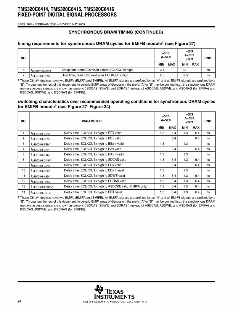
TMS320C6414, TMS320C6415, TMS320C6416FIXED-POINT DIGITAL SIGNAL PROCESSORS
SPRS146N − FEBRUARY 2001 − REVISED MAY 2005
94 POST OFFICE BOX 1443 • HOUSTON, TEXAS 77251−1443
SYNCHRONOUS DRAM TIMING (CONTINUED)
timing requirements for synchronous DRAM cycles for EMIFB module† (see Figure 27)
NO.
−5E0A−5E0
−6E3A−6E3−7E3 UNIT
MIN MAX MIN MAX
6 tsu(EDV-EKO1H) Setup time, read EDx valid before ECLKOUTx high 2.1 2.1 ns
7 th(EKO1H-EDV) Hold time, read EDx valid after ECLKOUTx high 2.5 2.5 ns† These C64x™ devices have two EMIFs (EMIFA and EMIFB). All EMIFA signals are prefixed by an “A” and all EMIFB signals are prefixed by a
“B”. Throughout the rest of this document, in generic EMIF areas of discussion, the prefix “A” or “B” may be omitted [e.g., the synchronous DRAMmemory access signals are shown as generic ( SDCAS, SDWE, and SDRAS ) instead of ASDCAS, ASDWE, and ASDRAS (for EMIFA) andBSDCAS, BSDWE, and BSDRAS (for EMIFB)].
switching characteristics over recommended operating conditions for synchronous DRAM cyclesfor EMIFB module† (see Figure 27−Figure 34)
NO. PARAMETER
−5E0A−5E0
−6E3A−6E3−7E3 UNIT
MIN MAX MIN MAX
1 td(EKO1H-CEV) Delay time, ECLKOUTx high to CEx valid 1.3 6.4 1.3 6.4 ns
2 td(EKO1H-BEV) Delay time, ECLKOUTx high to BEx valid 6.4 6.4 ns
3 td(EKO1H-BEIV) Delay time, ECLKOUTx high to BEx invalid 1.3 1.3 ns
4 td(EKO1H-EAV) Delay time, ECLKOUTx high to EAx valid 6.4 6.4 ns
5 td(EKO1H-EAIV) Delay time, ECLKOUTx high to EAx invalid 1.3 1.3 ns
8 td(EKO1H-CASV) Delay time, ECLKOUTx high to SDCAS valid 1.3 6.4 1.3 6.4 ns
9 td(EKO1H-EDV) Delay time, ECLKOUTx high to EDx valid 6.4 6.4 ns
10 td(EKO1H-EDIV) Delay time, ECLKOUTx high to EDx invalid 1.3 1.3 ns
11 td(EKO1H-WEV) Delay time, ECLKOUTx high to SDWE valid 1.3 6.4 1.3 6.4 ns
12 td(EKO1H-RAS) Delay time, ECLKOUTx high to SDRAS valid 1.3 6.4 1.3 6.4 ns
13 td(EKO1H-ACKEV) Delay time, ECLKOUTx high to ASDCKE valid (EMIFA only) 1.3 6.4 1.3 6.4 ns
14 td(EKO1H-PDTV) Delay time, ECLKOUTx high to PDT valid 1.3 6.4 1.3 6.4 ns† These C64x™ devices have two EMIFs (EMIFA and EMIFB). All EMIFA signals are prefixed by an “A” and all EMIFB signals are prefixed by a
“B”. Throughout the rest of this document, in generic EMIF areas of discussion, the prefix “A” or “B” may be omitted [e.g., the synchronous DRAMmemory access signals are shown as generic ( SDCAS, SDWE, and SDRAS ) instead of ASDCAS, ASDWE, and ASDRAS (for EMIFA) andBSDCAS, BSDWE, and BSDRAS (for EMIFB)].

TMS320C6414, TMS320C6415, TMS320C6416FIXED-POINT DIGITAL SIGNAL PROCESSORS
SPRS146N − FEBRUARY 2001 − REVISED MAY 2005
95POST OFFICE BOX 1443 • HOUSTON, TEXAS 77251−1443
SYNCHRONOUS DRAM TIMING (CONTINUED)
ECLKOUTx
CEx
ABE[7:0] or BBE[1:0]
AEA[12:3] or BEA[10:1]
AED[63:0] or BED[15:0]
AEA13 or BEA11
AOE/SDRAS/SOE‡
ARE/SDCAS/SADS/SRE‡
AWE/SDWE/SWE‡
AEA[22:14] or BEA[20:12]
BE1 BE2 BE3 BE4
Bank
Column
D1 D2 D3 D4
8
76
5
5
5
1
32
8
4
4
4
1
READ
PDT§1414
† These C64x™ devices have two EMIFs (EMIFA and EMIFB). All EMIFA signals are prefixed by an “A” and all EMIFB signals are prefixed by a“B”. Throughout the rest of this document, in generic EMIF areas of discussion, the prefix “A” or “B” may be omitted [e.g., the synchronous DRAMmemory access signals are shown as generic ( SDCAS, SDWE, and SDRAS ) instead of ASDCAS, ASDWE, and ASDRAS (for EMIFA) andBSDCAS, BSDWE, and BSDRAS (for EMIFB)].
‡ ARE/SDCAS/SADS/SRE, AWE/SDWE/SWE, and AOE/SDRAS/SOE operate as SDCAS, SDWE, and SDRAS, respectively, during SDRAMaccesses.
§ PDT signal is only asserted when the EDMA is in PDT mode (set the PDTS bit to 1 in the EDMA options parameter RAM). For PDT read, datais not latched into EMIF. The PDTRL field in the PDT control register (PDTCTL) configures the latency of the PDT signal with respect to the dataphase of a read transaction. The latency of the PDT signal for a read can be programmed to 0, 1, 2, or 3 by setting PDTRL to 00, 01, 10, or 11,respectively. PDTRL equals 00 (zero latency) in Figure 27.
Figure 27. SDRAM Read Command (CAS Latency 3) for EMIFA and EMIFB†

TMS320C6414, TMS320C6415, TMS320C6416FIXED-POINT DIGITAL SIGNAL PROCESSORS
SPRS146N − FEBRUARY 2001 − REVISED MAY 2005
96 POST OFFICE BOX 1443 • HOUSTON, TEXAS 77251−1443
SYNCHRONOUS DRAM TIMING (CONTINUED)
ECLKOUTx
CEx
ABE[7:0] or BBE[1:0]
AEA[12:3] or BEA[10:1]
AED[63:0] or BED[15:0]
AOE/SDRAS/SOE‡
ARE/SDCAS/SADS/SRE‡
AWE/SDWE/SWE‡
AEA13 or BEA11
AEA[22:14] or BEA[20:12]
BE1 BE2 BE3 BE4
Bank
Column
D1 D2 D3 D4
11
8
9
5
5
5
4
2
11
8
9
4
4
2
1
10
3
4
WRITE
PDT§
1414
† These C64x™ devices have two EMIFs (EMIFA and EMIFB). All EMIFA signals are prefixed by an “A” and all EMIFB signals are prefixed by a“B”. Throughout the rest of this document, in generic EMIF areas of discussion, the prefix “A” or “B” may be omitted [e.g., the synchronous DRAMmemory access signals are shown as generic ( SDCAS, SDWE, and SDRAS ) instead of ASDCAS, ASDWE, and ASDRAS (for EMIFA) andBSDCAS, BSDWE, and BSDRAS (for EMIFB)].
‡ ARE/SDCAS/SADS/SRE, AWE/SDWE/SWE, and AOE/SDRAS/SOE operate as SDCAS, SDWE, and SDRAS, respectively, during SDRAMaccesses.
§ PDT signal is only asserted when the EDMA is in PDT mode (set the PDTD bit to 1 in the EDMA options parameter RAM). For PDT write, datais not driven (in High-Z). The PDTWL field in the PDT control register (PDTCTL) configures the latency of the PDT signal with respect to the dataphase of a write transaction. The latency of the PDT signal for a write transaction can be programmed to 0, 1, 2, or 3 by setting PDTWL to 00,01, 10, or 11, respectively. PDTWL equals 00 (zero latency) in Figure 28.
Figure 28. SDRAM Write Command for EMIFA and EMIFB†

TMS320C6414, TMS320C6415, TMS320C6416FIXED-POINT DIGITAL SIGNAL PROCESSORS
SPRS146N − FEBRUARY 2001 − REVISED MAY 2005
97POST OFFICE BOX 1443 • HOUSTON, TEXAS 77251−1443
SYNCHRONOUS DRAM TIMING (CONTINUED)
ECLKOUTx
CEx
ABE[7:0] or BBE[1:0]
AEA[22:14] or BEA[20:12]
AED[63:0] or BED[15:0]
AEA13 or BEA11
AOE/SDRAS/SOE‡
ARE/SDCAS/SADS/SRE‡
AWE/SDWE/SWE‡
Bank Activate
Row Address
Row Address
12
5
5
5
1
AEA[12:3] or BEA[10:1]
ACTV
12
4
4
4
1
† These C64x™ devices have two EMIFs (EMIFA and EMIFB). All EMIFA signals are prefixed by an “A” and all EMIFB signals are prefixed by a“B”. Throughout the rest of this document, in generic EMIF areas of discussion, the prefix “A” or “B” may be omitted [e.g., the synchronous DRAMmemory access signals are shown as generic ( SDCAS, SDWE, and SDRAS ) instead of ASDCAS, ASDWE, and ASDRAS (for EMIFA) andBSDCAS, BSDWE, and BSDRAS (for EMIFB)].
‡ ARE/SDCAS/SADS/SRE, AWE/SDWE/SWE, and AOE/SDRAS/SOE operate as SDCAS, SDWE, and SDRAS, respectively, during SDRAMaccesses.
Figure 29. SDRAM ACTV Command for EMIFA and EMFB†

TMS320C6414, TMS320C6415, TMS320C6416FIXED-POINT DIGITAL SIGNAL PROCESSORS
SPRS146N − FEBRUARY 2001 − REVISED MAY 2005
98 POST OFFICE BOX 1443 • HOUSTON, TEXAS 77251−1443
SYNCHRONOUS DRAM TIMING (CONTINUED)
ECLKOUTx
CEx
ABE[7:0] or BBE[1:0]
AEA[22:14, 12:3] orBEA[20:12, 10:1]
AED[63:0] or BED[15:0]
AEA13 or BEA11
AOE/SDRAS/SOE‡
ARE/SDCAS/SADS/SRE‡
AWE/SDWE/SWE‡
11
12
5
1
DCAB
11
12
4
1
† These C64x™ devices have two EMIFs (EMIFA and EMIFB). All EMIFA signals are prefixed by an “A” and all EMIFB signals are prefixed by a“B”. Throughout the rest of this document, in generic EMIF areas of discussion, the prefix “A” or “B” may be omitted [e.g., the synchronous DRAMmemory access signals are shown as generic ( SDCAS, SDWE, and SDRAS ) instead of ASDCAS, ASDWE, and ASDRAS (for EMIFA) andBSDCAS, BSDWE, and BSDRAS (for EMIFB)].
‡ ARE/SDCAS/SADS/SRE, AWE/SDWE/SWE, and AOE/SDRAS/SOE operate as SDCAS, SDWE, and SDRAS, respectively, during SDRAMaccesses.
Figure 30. SDRAM DCAB Command for EMIFA and EMIFB†
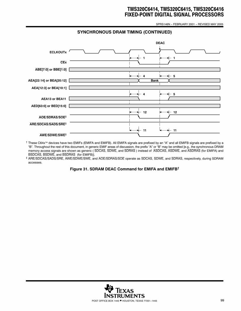
TMS320C6414, TMS320C6415, TMS320C6416FIXED-POINT DIGITAL SIGNAL PROCESSORS
SPRS146N − FEBRUARY 2001 − REVISED MAY 2005
99POST OFFICE BOX 1443 • HOUSTON, TEXAS 77251−1443
SYNCHRONOUS DRAM TIMING (CONTINUED)
ECLKOUTx
CEx
ABE[7:0] or BBE[1:0]
AEA[22:14] or BEA[20:12]
AED[63:0] or BED[15:0]
AEA13 or BEA11
AOE/SDRAS/SOE‡
ARE/SDCAS/SADS/SRE‡
AWE/SDWE/SWE‡
AEA[12:3] or BEA[10:1]
Bank
11
12
5
5
1
DEAC
11
12
4
4
1
† These C64x™ devices have two EMIFs (EMIFA and EMIFB). All EMIFA signals are prefixed by an “A” and all EMIFB signals are prefixed by a“B”. Throughout the rest of this document, in generic EMIF areas of discussion, the prefix “A” or “B” may be omitted [e.g., the synchronous DRAMmemory access signals are shown as generic ( SDCAS, SDWE, and SDRAS ) instead of ASDCAS, ASDWE, and ASDRAS (for EMIFA) andBSDCAS, BSDWE, and BSDRAS (for EMIFB)].
‡ ARE/SDCAS/SADS/SRE, AWE/SDWE/SWE, and AOE/SDRAS/SOE operate as SDCAS, SDWE, and SDRAS, respectively, during SDRAMaccesses.
Figure 31. SDRAM DEAC Command for EMIFA and EMIFB†

TMS320C6414, TMS320C6415, TMS320C6416FIXED-POINT DIGITAL SIGNAL PROCESSORS
SPRS146N − FEBRUARY 2001 − REVISED MAY 2005
100 POST OFFICE BOX 1443 • HOUSTON, TEXAS 77251−1443
SYNCHRONOUS DRAM TIMING (CONTINUED)
ECLKOUTx
CEx
ABE[7:0] or BBE[1:0]
AEA[22:14, 12:3] orBEA[20:12, 10:1]
AED[63:0] or BED[15:0]
AEA13 or BEA11
AOE/SDRAS/SOE‡
ARE/SDCAS/SADS/SRE‡
AWE/SDWE/SWE‡
8
12
1
REFR
8
12
1
† These C64x™ devices have two EMIFs (EMIFA and EMIFB). All EMIFA signals are prefixed by an “A” and all EMIFB signals are prefixed by a“B”. Throughout the rest of this document, in generic EMIF areas of discussion, the prefix “A” or “B” may be omitted [e.g., the synchronous DRAMmemory access signals are shown as generic ( SDCAS, SDWE, and SDRAS ) instead of ASDCAS, ASDWE, and ASDRAS (for EMIFA) andBSDCAS, BSDWE, and BSDRAS (for EMIFB)].
‡ ARE/SDCAS/SADS/SRE, AWE/SDWE/SWE, and AOE/SDRAS/SOE operate as SDCAS, SDWE, and SDRAS, respectively, during SDRAMaccesses.
Figure 32. SDRAM REFR Command for EMIFA and EMIFB†
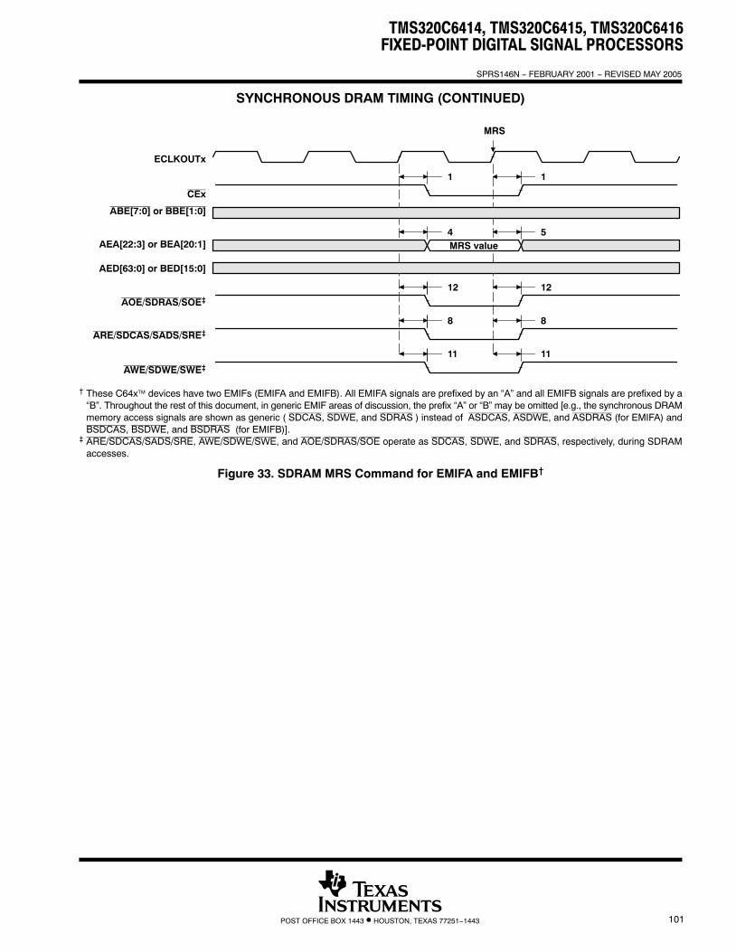
TMS320C6414, TMS320C6415, TMS320C6416FIXED-POINT DIGITAL SIGNAL PROCESSORS
SPRS146N − FEBRUARY 2001 − REVISED MAY 2005
101POST OFFICE BOX 1443 • HOUSTON, TEXAS 77251−1443
SYNCHRONOUS DRAM TIMING (CONTINUED)
ECLKOUTx
CEx
ABE[7:0] or BBE[1:0]
AEA[22:3] or BEA[20:1]
AED[63:0] or BED[15:0]
AOE/SDRAS/SOE‡
ARE/SDCAS/SADS/SRE‡
AWE/SDWE/SWE‡
MRS value
11
8
12
5
1
MRS
11
8
12
4
1
† These C64x™ devices have two EMIFs (EMIFA and EMIFB). All EMIFA signals are prefixed by an “A” and all EMIFB signals are prefixed by a“B”. Throughout the rest of this document, in generic EMIF areas of discussion, the prefix “A” or “B” may be omitted [e.g., the synchronous DRAMmemory access signals are shown as generic ( SDCAS, SDWE, and SDRAS ) instead of ASDCAS, ASDWE, and ASDRAS (for EMIFA) andBSDCAS, BSDWE, and BSDRAS (for EMIFB)].
‡ ARE/SDCAS/SADS/SRE, AWE/SDWE/SWE, and AOE/SDRAS/SOE operate as SDCAS, SDWE, and SDRAS, respectively, during SDRAMaccesses.
Figure 33. SDRAM MRS Command for EMIFA and EMIFB†
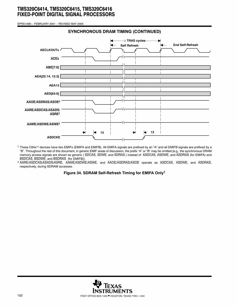
TMS320C6414, TMS320C6415, TMS320C6416FIXED-POINT DIGITAL SIGNAL PROCESSORS
SPRS146N − FEBRUARY 2001 − REVISED MAY 2005
102 POST OFFICE BOX 1443 • HOUSTON, TEXAS 77251−1443
SYNCHRONOUS DRAM TIMING (CONTINUED)
End Self-RefreshSelf Refresh
1313
AECLKOUTx
ACEx
ABE[7:0]
AEA[22:14, 12:3]
AEA13
AED[63:0]
AAOE/ASDRAS/ASOE‡
AARE/ASDCAS/ASADS/ASRE‡
AAWE/ASDWE/ASWE‡
ASDCKE
≥ TRAS cycles
† These C64x™ devices have two EMIFs (EMIFA and EMIFB). All EMIFA signals are prefixed by an “A” and all EMIFB signals are prefixed by a“B”. Throughout the rest of this document, in generic EMIF areas of discussion, the prefix “A” or “B” may be omitted [e.g., the synchronous DRAMmemory access signals are shown as generic ( SDCAS, SDWE, and SDRAS ) instead of ASDCAS, ASDWE, and ASDRAS (for EMIFA) andBSDCAS, BSDWE, and BSDRAS (for EMIFB)].
‡ AARE/ASDCAS/ASADS/ASRE, AAWE/ASDWE/ASWE, and AAOE/ASDRAS/ASOE operate as ASDCAS, ASDWE, and ASDRAS,respectively, during SDRAM accesses.
Figure 34. SDRAM Self-Refresh Timing for EMIFA Only†
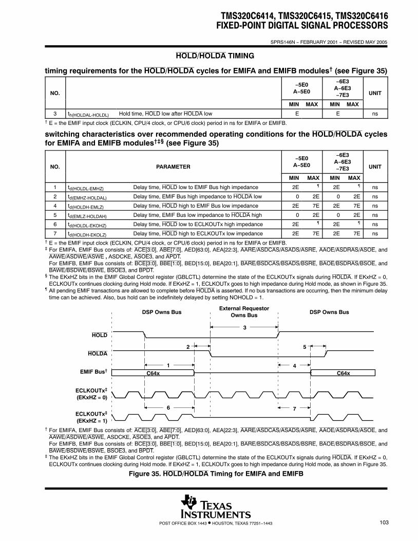
TMS320C6414, TMS320C6415, TMS320C6416FIXED-POINT DIGITAL SIGNAL PROCESSORS
SPRS146N − FEBRUARY 2001 − REVISED MAY 2005
103POST OFFICE BOX 1443 • HOUSTON, TEXAS 77251−1443
HOLD/HOLDA TIMING
timing requirements for the HOLD/HOLDA cycles for EMIFA and EMIFB modules† (see Figure 35)
NO.
−5E0A−5E0
−6E3A−6E3−7E3 UNIT
MIN MAX MIN MAX
3 th(HOLDAL-HOLDL) Hold time, HOLD low after HOLDA low E E ns† E = the EMIF input clock (ECLKIN, CPU/4 clock, or CPU/6 clock) period in ns for EMIFA or EMIFB.
switching characteristics over recommended operating conditions for the HOLD/HOLDA cyclesfor EMIFA and EMIFB modules†‡§ (see Figure 35)
NO. PARAMETER
−5E0A−5E0
−6E3A−6E3−7E3 UNIT
MIN MAX MIN MAX
1 td(HOLDL-EMHZ) Delay time, HOLD low to EMIF Bus high impedance 2E ¶ 2E ¶ ns
2 td(EMHZ-HOLDAL) Delay time, EMIF Bus high impedance to HOLDA low 0 2E 0 2E ns
4 td(HOLDH-EMLZ) Delay time, HOLD high to EMIF Bus low impedance 2E 7E 2E 7E ns
5 td(EMLZ-HOLDAH) Delay time, EMIF Bus low impedance to HOLDA high 0 2E 0 2E ns
6 td(HOLDL-EKOHZ) Delay time, HOLD low to ECLKOUTx high impedance 2E ¶ 2E ¶ ns
7 td(HOLDH-EKOLZ) Delay time, HOLD high to ECLKOUTx low impedance 2E 7E 2E 7E ns† E = the EMIF input clock (ECLKIN, CPU/4 clock, or CPU/6 clock) period in ns for EMIFA or EMIFB.‡ For EMIFA, EMIF Bus consists of: ACE[3:0], ABE[7:0], AED[63:0], AEA[22:3], AARE/ASDCAS/ASADS/ASRE, AAOE/ASDRAS/ASOE, and
AAWE/ASDWE/ASWE , ASDCKE, ASOE3, and APDT.For EMIFB, EMIF Bus consists of: BCE[3:0], BBE[1:0], BED[15:0], BEA[20:1], BARE/BSDCAS/BSADS/BSRE, BAOE/BSDRAS/BSOE, andBAWE/BSDWE/BSWE, BSOE3, and BPDT.
§ The EKxHZ bits in the EMIF Global Control register (GBLCTL) determine the state of the ECLKOUTx signals during HOLDA. If EKxHZ = 0,ECLKOUTx continues clocking during Hold mode. If EKxHZ = 1, ECLKOUTx goes to high impedance during Hold mode, as shown in Figure 35.
¶ All pending EMIF transactions are allowed to complete before HOLDA is asserted. If no bus transactions are occurring, then the minimum delaytime can be achieved. Also, bus hold can be indefinitely delayed by setting NOHOLD = 1.
HOLD
HOLDA
EMIF Bus†
DSP Owns BusExternal Requestor
Owns Bus DSP Owns Bus
C64x C64x1
3
2 5
4
ECLKOUTx‡
(EKxHZ = 0)
ECLKOUTx‡
(EKxHZ = 1)
6 7
† For EMIFA, EMIF Bus consists of: ACE[3:0], ABE[7:0], AED[63:0], AEA[22:3], AARE/ASDCAS/ASADS/ASRE, AAOE/ASDRAS/ASOE, andAAWE/ASDWE/ASWE, ASDCKE, ASOE3, and APDT.For EMIFB, EMIF Bus consists of: BCE[3:0], BBE[1:0], BED[15:0], BEA[20:1], BARE/BSDCAS/BSADS/BSRE, BAOE/BSDRAS/BSOE, andBAWE/BSDWE/BSWE, BSOE3, and BPDT.
‡ The EKxHZ bits in the EMIF Global Control register (GBLCTL) determine the state of the ECLKOUTx signals during HOLDA. If EKxHZ = 0,ECLKOUTx continues clocking during Hold mode. If EKxHZ = 1, ECLKOUTx goes to high impedance during Hold mode, as shown in Figure 35.
Figure 35. HOLD/HOLDA Timing for EMIFA and EMIFB

TMS320C6414, TMS320C6415, TMS320C6416FIXED-POINT DIGITAL SIGNAL PROCESSORS
SPRS146N − FEBRUARY 2001 − REVISED MAY 2005
104 POST OFFICE BOX 1443 • HOUSTON, TEXAS 77251−1443
BUSREQ TIMING
switching characteristics over recommended operating conditions for the BUSREQ cyclesfor EMIFA and EMIFB modules (see Figure 36)
NO. PARAMETER
−5E0A−5E0
−6E3A−6E3−7E3 UNIT
MIN MAX MIN MAX
1 td(AEKO1H-ABUSRV) Delay time, AECLKOUTx high to ABUSREQ valid 0.6 7.1 1 5.5 ns
2 td(BEKO1H-BBUSRV) Delay time, BECLKOUTx high to BBUSREQ valid 0.5 6.9 0.9 5.5 ns
ECLKOUTx
1
ABUSREQ
1
2 2
BBUSREQ
Figure 36. BUSREQ Timing for EMIFA and EMIFB

TMS320C6414, TMS320C6415, TMS320C6416FIXED-POINT DIGITAL SIGNAL PROCESSORS
SPRS146N − FEBRUARY 2001 − REVISED MAY 2005
105POST OFFICE BOX 1443 • HOUSTON, TEXAS 77251−1443
RESET TIMING timing requirements for reset† (see Figure 37)
NO.
−5E0, A−5E0,−6E3, A−6E3, −7E3 UNITNO.
MIN MAXUNIT
1 tWidth of the RESET pulse (PLL stable)‡ 10P ns
1 tw(RST) Width of the RESET pulse (PLL needs to sync up)§ 250 µs
16 tsu(boot) Setup time, boot configuration bits valid before RESET high¶ 4E or 4C# ns
17 th(boot) Hold time, boot configuration bits valid after RESET high¶ 4P ns
18 tsu(PCLK-RSTH) Setup time, PCLK active before RESET high|| 32N ns† P = 1/CPU clock frequency in ns. For example, when running parts at 600 MHz, use P = 1.67 ns.‡ This parameter applies to CLKMODE x1 when CLKIN is stable, and applies to CLKMODE x6, x12 when CLKIN and PLL are stable.§ This parameter applies to CLKMODE x6, x12 only (it does not apply to CLKMODE x1). The RESET signal is not connected internally to the clock
PLL circuit. The PLL, however, may need up to 250 µs to stabilize following device power up or after PLL configuration has been changed. Duringthat time, RESET must be asserted to ensure proper device operation. See the clock PLL section for PLL lock times.
¶ EMIFB address pins BEA[20:13, 11, 7] are the boot configuration pins during device reset.# E = 1/AECLKIN clock frequency in ns. C = 1/CLKIN clock frequency in ns. Select whichever value is larger for the MIN parameter.|| N = the PCI input clock (PCLK) period in ns. When PCI is enabled (PCI_EN = 1), this parameter must be met.
switching characteristics over recommended operating conditions during reset† (see Figure 37)
NO. PARAMETER
−5E0, A−5E0,−6E3, A−6E3, −7E3 UNITNO. PARAMETER
MIN MAXUNIT
2 td(RSTL-ECKI) Delay time, RESET low to ECLKIN synchronized internally 2E 3P + 20E ns
3 td(RSTH-ECKI) Delay time, RESET high to ECLKIN synchronized internally 2E 8P + 20E ns
4 td(RSTL-ECKO1HZ) Delay time, RESET low to ECLKOUT1 high impedance 2E ns
5 td(RSTH-ECKO1V) Delay time, RESET high to ECLKOUT1 valid 8P + 20E ns
6 td(RSTL-EMIFZHZ) Delay time, RESET low to EMIF Z high impedance 2E 3P + 4E ns
7 td(RSTH-EMIFZV) Delay time, RESET high to EMIF Z valid 16E 8P + 20E ns
8 td(RSTL-EMIFHIV) Delay time, RESET low to EMIF high group invalid 2E ns
9 td(RSTH-EMIFHV) Delay time, RESET high to EMIF high group valid 8P + 20E ns
10 td(RSTL-EMIFLIV) Delay time, RESET low to EMIF low group invalid 2E ns
11 td(RSTH-EMIFLV) Delay time, RESET high to EMIF low group valid 8P + 20E ns
12 td(RSTL-LOWIV) Delay time, RESET low to low group invalid 0 ns
13 td(RSTH-LOWV) Delay time, RESET high to low group valid 11P ns
14 td(RSTL-ZHZ) Delay time, RESET low to Z group high impedance 0 ns
15 td(RSTH-ZV) Delay time, RESET high to Z group valid 2P 8P ns
† P = 1/CPU clock frequency in ns. For example, when running parts at 600 MHz, use P = 1.67 ns. E = the EMIF input clock (ECLKIN, CPU/4 clock, or CPU/6 clock) period in ns for EMIFA or EMIFB. EMIF Z group consists of: AEA[22:3], BEA[20:1], AED[63:0], BED[15:0], CE[3:0], ABE[7:0], BBE[1:0], ARE/SDCAS/SADS/SRE,
AWE/SDWE/SWE, and AOE/SDRAS/SOE, SOE3, ASDCKE, and PDT.EMIF high group consists of: AHOLDA and BHOLDA (when the corresponding HOLD input is high)EMIF low group consists of: ABUSREQ and BBUSREQ; AHOLDA and BHOLDA (when the corresponding HOLD input is low)Low group consists of: XSP_CS, CLKX2/XSP_CLK, and DX2/XSP_DO; all of which apply only when PCI EEPROM (BEA13)
is enabled (with PCI_EN = 1 and MCBSP2_EN = 0). Otherwise, the CLKX2/XSP_CLK and DX2/XSP_DO pins are in the Z group. For more details on the PCI configuration pins, see the Device Configurations section of this data sheet.
Z group consists of: HD[31:0]/AD[31:0], CLKX0, CLKX1/URADDR4, CLKX2/XSP_CLK, FSX0, FSX1/UXADDR3, FSX2, DX0, DX1/UXADDR4, DX2/XSP_DO, CLKR0, CLKR1/URADDR2, CLKR2, FSR0, FSR1/UXADDR2, FSR2, TOUT0, TOUT1, TOUT2, GP[8:0], GP10/PCBE3, HR/W/PCBE2, HDS2/PCBE1, PCBE0, GP13/PINTA, GP11/PREQ, HDS1/PSERR, HCS/PPERR, HCNTL1/PDEVSEL, HAS/PPAR, HCNTL0/PSTOP, HHWIL/PTRDY (16-bit HPI mode only), HRDY/PIRDY, HINT/PFRAME, UXDATA[7:0], UXSOC, UXCLAV, and URCLAV.

TMS320C6414, TMS320C6415, TMS320C6416FIXED-POINT DIGITAL SIGNAL PROCESSORS
SPRS146N − FEBRUARY 2001 − REVISED MAY 2005
106 POST OFFICE BOX 1443 • HOUSTON, TEXAS 77251−1443
RESET TIMING (CONTINUED)
ECLKOUT2
17
14
1
CLKOUT4
CLKOUT6
RESET
ECLKIN
Low Group‡
Z Group‡§Boot and Device
Configuration Inputs§¶16
15
32
10
8
EMIF Z Group‡§
EMIF High Group‡
EMIF Low Group‡
11
9
76
1312
ECLKOUT1
54
PCLK
18
† These C64x™ devices have two EMIFs (EMIFA and EMIFB). All EMIFA signals are prefixed by an “A” and all EMIFB signals are prefixed by a“B”. Throughout the rest of this document, in generic EMIF areas of discussion, the prefix “A” or “B” may be omitted [e.g., ECLKIN, ECLKOUT1,and ECLKOUT2].
‡ EMIF Z group consists of: AEA[22:3], BEA[20:1], AED[63:0], BED[15:0], CE[3:0], ABE[7:0], BBE[1:0], ARE/SDCAS/SADS/SRE,AWE/SDWE/SWE, and AOE/SDRAS/SOE, SOE3, ASDCKE, and PDT.
EMIF high group consists of: AHOLDA and BHOLDA (when the corresponding HOLD input is high)EMIF low group consists of: ABUSREQ and BBUSREQ; AHOLDA and BHOLDA (when the corresponding HOLD input is low)Low group consists of: XSP_CS, CLKX2/XSP_CLK, and DX2/XSP_DO; all of which apply only when PCI EEPROM (BEA13)
is enabled (with PCI_EN = 1 and MCBSP2_EN = 0). Otherwise, the CLKX2/XSP_CLK and DX2/XSP_DO pins are in the Z group. For more details on the PCI configuration pins, see the Device Configurations section of this data sheet.
Z group consists of: HD[31:0]/AD[31:0], CLKX0, CLKX1/URADDR4, CLKX2/XSP_CLK, FSX0, FSX1/UXADDR3, FSX2, DX0, DX1/UXADDR4, DX2/XSP_DO, CLKR0, CLKR1/URADDR2, CLKR2, FSR0, FSR1/UXADDR2, FSR2, TOUT0, TOUT1, TOUT2, GP[8:0], GP10/PCBE3, HR/W/PCBE2, HDS2/PCBE1, PCBE0, GP13/PINTA, GP11/PREQ, HDS1/PSERR, HCS/PPERR, HCNTL1/PDEVSEL, HAS/PPAR, HCNTL0/PSTOP, HHWIL/PTRDY (16-bit HPI mode only), HRDY/PIRDY, HINT/PFRAME, UXDATA[7:0], UXSOC, UXCLAV, and URCLAV.
§ If BEA[20:13, 11, 7] and HD5/AD5 pins are actively driven, care must be taken to ensure no timing contention between parameters 6, 7, 14, 15,16, and 17.
¶ Boot and Device Configurations Inputs (during reset) include: EMIFB address pins BEA[20:13, 11, 7] and HD5/AD5. The PCI_EN pin must be driven valid at all times and the user must not switch values throughout device operation. The MCBSP2_EN pin must be driven valid at all times and the user can switch values throughout device operation.
Figure 37. Reset Timing†

TMS320C6414, TMS320C6415, TMS320C6416FIXED-POINT DIGITAL SIGNAL PROCESSORS
SPRS146N − FEBRUARY 2001 − REVISED MAY 2005
107POST OFFICE BOX 1443 • HOUSTON, TEXAS 77251−1443
EXTERNAL INTERRUPT TIMING
timing requirements for external interrupts† (see Figure 38)
NO.
−5E0, A−5E0,−6E3, A−6E3,
−7E3 UNIT
MIN MAX
1 tWidth of the NMI interrupt pulse low 4P ns
1 tw(ILOW) Width of the EXT_INT interrupt pulse low 8P ns
2 tWidth of the NMI interrupt pulse high 4P ns
2 tw(IHIGH)Width of the EXT_INT interrupt pulse high 8P ns
† P = 1/CPU clock frequency in ns. For example, when running parts at 600 MHz, use P = 1.67 ns.
21
EXT_INTx, NMI
Figure 38. External/NMI Interrupt Timing

TMS320C6414, TMS320C6415, TMS320C6416FIXED-POINT DIGITAL SIGNAL PROCESSORS
SPRS146L − FEBRUARY 2001 − REVISED JULY 2004
108 POST OFFICE BOX 1443 • HOUSTON, TEXAS 77251−1443
HOST-PORT INTERFACE (HPI) TIMING
timing requirements for host-port interface cycles†‡ (see Figure 39 through Figure 46)
NO.
−5E0, A−5E0,−6E3, A−6E3,
−7E3 UNIT
MIN MAX
1 tsu(SELV-HSTBL) Setup time, select signals§ valid before HSTROBE low 5 ns
2 th(HSTBL-SELV) Hold time, select signals§ valid after HSTROBE low 2.4 ns
3 tw(HSTBL) Pulse duration, HSTROBE low 4P¶ ns
4 tw(HSTBH) Pulse duration, HSTROBE high between consecutive accesses 4P ns
10 tsu(SELV-HASL) Setup time, select signals§ valid before HAS low 5 ns
11 th(HASL-SELV) Hold time, select signals§ valid after HAS low 2 ns
12 tsu(HDV-HSTBH) Setup time, host data valid before HSTROBE high 5 ns
13 th(HSTBH-HDV) Hold time, host data valid after HSTROBE high 2.8 ns
14 th(HRDYL-HSTBL)
Hold time, HSTROBE low after HRDY low. HSTROBE should not be
inactivated until HRDY is active (low); otherwise, HPI writes will not complete
properly.
2 ns
18 tsu(HASL-HSTBL) Setup time, HAS low before HSTROBE low 2 ns
19 th(HSTBL-HASL) Hold time, HAS low after HSTROBE low 2.1 ns† HSTROBE refers to the following logical operation on HCS, HDS1, and HDS2: [NOT(HDS1 XOR HDS2)] OR HCS.‡ P = 1/CPU clock frequency in ns. For example, when running parts at 600 MHz, use P = 1.67 ns.§ Select signals include: HCNTL[1:0] and HR/W. For HPI16 mode only, select signals also include HHWIL.¶ Select the parameter value of 4P or 12.5 ns, whichever is greater.
switching characteristics over recommended operating conditions during host-port interfacecycles†‡ (see Figure 39 through Figure 46)
NO. PARAMETER
−5E0−6E3−7E3
A−5E0A−6E3 UNIT
MIN MAX MIN MAX
6 td(HSTBL-HRDYH) Delay time, HSTROBE low to HRDY high# 1.3 4P + 8 1.3 4P + 9 ns
7 td(HSTBL-HDLZ)Delay time, HSTROBE low to HD low impedance for an HPI read
2 2 ns
8 td(HDV-HRDYL) Delay time, HD valid to HRDY low −3 −3 ns
9 toh(HSTBH-HDV) Output hold time, HD valid after HSTROBE high 1.5 1.5 ns
15 td(HSTBH-HDHZ) Delay time, HSTROBE high to HD high impedance 12 12 ns
16 td(HSTBL-HDV)Delay time, HSTROBE low to HD valid (HPI16 mode, 2nd half-word only)
4P + 8 4P + 8 ns
† HSTROBE refers to the following logical operation on HCS, HDS1, and HDS2: [NOT(HDS1 XOR HDS2)] OR HCS.‡ P = 1/CPU clock frequency in ns. For example, when running parts at 600 MHz, use P = 1.67 ns.# This parameter is used during HPID reads and writes. For reads, at the beginning of a word transfer (HPI32) or the first half-word transfer (HPI16)
on the falling edge of HSTROBE, the HPI sends the request to the EDMA internal address generation hardware, and HRDY remains high untilthe EDMA internal address generation hardware loads the requested data into HPID. For writes, HRDY goes high if the internal write buffer isfull.

TMS320C6414, TMS320C6415, TMS320C6416FIXED-POINT DIGITAL SIGNAL PROCESSORS
SPRS146L − FEBRUARY 2001 − REVISED JULY 2004
109POST OFFICE BOX 1443 • HOUSTON, TEXAS 77251−1443
HOST-PORT INTERFACE (HPI) TIMING (CONTINUED)
1st half-word 2nd half-word86
15916
1597
43
21
21
21
21
21
21
HAS
HCNTL[1:0]
HR/W
HHWIL
HSTROBE†
HCS
HD[15:0] (output)
HRDY
3
† HSTROBE refers to the following logical operation on HCS, HDS1, and HDS2: [NOT(HDS1 XOR HDS2)] OR HCS.
Figure 39. HPI16 Read Timing (HAS Not Used, Tied High)
HAS†
HCNTL[1:0]
HR/W
HHWIL
HSTROBE‡
HCS
HD[15:0] (output)
HRDY
1st half-word 2nd half-word86
15916
1597
43
11
1011
10
1110
1110
111011
1019 19
1818
† For correct operation, strobe the HAS signal only once per HSTROBE active cycle.‡ HSTROBE refers to the following logical operation on HCS, HDS1, and HDS2: [NOT(HDS1 XOR HDS2)] OR HCS.
Figure 40. HPI16 Read Timing (HAS Used)

TMS320C6414, TMS320C6415, TMS320C6416FIXED-POINT DIGITAL SIGNAL PROCESSORS
SPRS146L − FEBRUARY 2001 − REVISED JULY 2004
110 POST OFFICE BOX 1443 • HOUSTON, TEXAS 77251−1443
HOST-PORT INTERFACE (HPI) TIMING (CONTINUED)
1st half-word 2nd half-word
1312
1312
4
14
3
21
21
21
21
21
21
HAS
HCNTL[1:0]
HR/W
HHWIL
HSTROBE†
HCS
HD[15:0] (input)
HRDY
3
6
† HSTROBE refers to the following logical operation on HCS, HDS1, and HDS2: [NOT(HDS1 XOR HDS2)] OR HCS.
Figure 41. HPI16 Write Timing (HAS Not Used, Tied High)
1st half-word 2nd half-word
1312
1312
4
14
3
1110
1110
1110
1110
1110
1110
HAS†
HCNTL[1:0]
HR/W
HHWIL
HSTROBE‡
HCS
HD[15:0] (input)
HRDY
1919
18 18
6
† For correct operation, strobe the HAS signal only once per HSTROBE active cycle.‡ HSTROBE refers to the following logical operation on HCS, HDS1, and HDS2: [NOT(HDS1 XOR HDS2)] OR HCS.
Figure 42. HPI16 Write Timing (HAS Used)
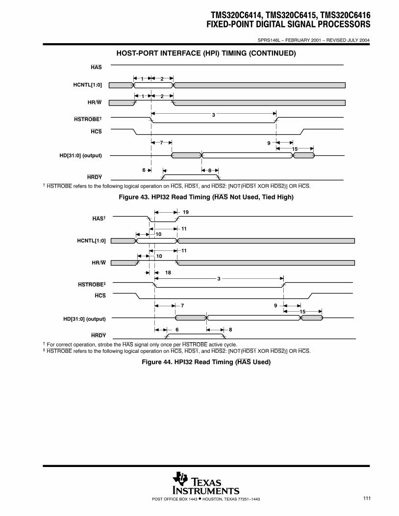
TMS320C6414, TMS320C6415, TMS320C6416FIXED-POINT DIGITAL SIGNAL PROCESSORS
SPRS146L − FEBRUARY 2001 − REVISED JULY 2004
111POST OFFICE BOX 1443 • HOUSTON, TEXAS 77251−1443
HOST-PORT INTERFACE (HPI) TIMING (CONTINUED)
6
3
HAS
HCNTL[1:0]
HR/W
HSTROBE†
HCS
HD[31:0] (output)
HRDY8
97
21
21
15
† HSTROBE refers to the following logical operation on HCS, HDS1, and HDS2: [NOT(HDS1 XOR HDS2)] OR HCS.
Figure 43. HPI32 Read Timing (HAS Not Used, Tied High)
86
1597
318
1110
1110
19HAS†
HCNTL[1:0]
HR/W
HSTROBE‡
HCS
HD[31:0] (output)
HRDY† For correct operation, strobe the HAS signal only once per HSTROBE active cycle.‡ HSTROBE refers to the following logical operation on HCS, HDS1, and HDS2: [NOT(HDS1 XOR HDS2)] OR HCS.
Figure 44. HPI32 Read Timing (HAS Used)

TMS320C6414, TMS320C6415, TMS320C6416FIXED-POINT DIGITAL SIGNAL PROCESSORS
SPRS146L − FEBRUARY 2001 − REVISED JULY 2004
112 POST OFFICE BOX 1443 • HOUSTON, TEXAS 77251−1443
HOST-PORT INTERFACE (HPI) TIMING (CONTINUED)
1312
14
3
21
21
HAS
HCNTL[1:0]
HR/W
HSTROBE†
HCS
HD[31:0] (input)
HRDY6
† HSTROBE refers to the following logical operation on HCS, HDS1, and HDS2: [NOT(HDS1 XOR HDS2)] OR HCS.
Figure 45. HPI32 Write Timing (HAS Not Used, Tied High)
1312
14
318
1110
1110
19
HAS†
HCNTL[1:0]
HR/W
HSTROBE‡
HCS
HD[31:0] (input)
HRDY6
† For correct operation, strobe the HAS signal only once per HSTROBE active cycle.‡ HSTROBE refers to the following logical operation on HCS, HDS1, and HDS2: [NOT(HDS1 XOR HDS2)] OR HCS.
Figure 46. HPI32 Write Timing (HAS Used)

TMS320C6414, TMS320C6415, TMS320C6416FIXED-POINT DIGITAL SIGNAL PROCESSORS
SPRS146L − FEBRUARY 2001 − REVISED JULY 2004
113POST OFFICE BOX 1443 • HOUSTON, TEXAS 77251−1443
PERIPHERAL COMPONENT INTERCONNECT (PCI) TIMING [C6415 AND C6416 ONLY]
timing requirements for PCLK†‡ (see Figure 47)
NO.
−5E0, A−5E0,−6E3, A−6E3,
−7E3 UNIT
MIN MAX
1 tc(PCLK) Cycle time, PCLK 30 (or 8P§) ns
2 tw(PCLKH) Pulse duration, PCLK high 11 ns
3 tw(PCLKL) Pulse duration, PCLK low 11 ns
4 tsr(PCLK) ∆v/∆t slew rate, PCLK 1 4 V/ns† For 3.3-V operation, the reference points for the rise and fall transitions are measured at VILP MAX and VIHP MIN.‡ P = 1/CPU clock frequency in ns. For example when running parts at 600 MHz, use P = 1.67 ns.§ Select the parameter value of 30 ns or 8P, whichever is greater.
PCLK
1
2
3
4
4
0.4 DVDD V MINPeak to Peak for3.3V signaling
Figure 47. PCLK Timing
timing requirements for PCI reset (see Figure 48)
NO.
−5E0, A−5E0,−6E3, A−6E3,
−7E3 UNIT
MIN MAX
1 tw(PRST) Pulse duration, PRST 1 ms
2 tsu(PCLKA-PRSTH) Setup time, PCLK active before PRST high 100 µs
PRST
PCLK
2
1
Figure 48. PCI Reset (PRST) Timing

TMS320C6414, TMS320C6415, TMS320C6416FIXED-POINT DIGITAL SIGNAL PROCESSORS
SPRS146L − FEBRUARY 2001 − REVISED JULY 2004
114 POST OFFICE BOX 1443 • HOUSTON, TEXAS 77251−1443
PERIPHERAL COMPONENT INTERCONNECT (PCI) TIMING [C6415 AND C6416 ONLY] (CONTINUED)
timing requirements for PCI inputs (see Figure 49)
NO.
−5E0, A−5E0,−6E3, A−6E3,
−7E3 UNIT
MIN MAX
5 tsu(IV-PCLKH) Setup time, input valid before PCLK high 7 ns
6 th(IV-PCLKH) Hold time, input valid after PCLK high 0 ns
switching characteristics over recommended operating conditions for PCI outputs (see Figure 49)
NO. PARAMETER
−5E0, A−5E0,−6E3, A−6E3,
−7E3 UNIT
MIN MAX
1 td(PCLKH-OV) Delay time, PCLK high to output valid 11 ns
2 td(PCLKH-OIV) Delay time, PCLK high to output invalid 2 ns
3 td(PCLKH-OLZ) Delay time, PCLK high to output low impedance 2 ns
4 td(PCLKH-OHZ) Delay time, PCLK high to output high impedance 28 ns
Valid
PCLK
5
PCI Output
PCI Input
3
Valid
2
6
1
4
Figure 49. PCI Input/Output Timing
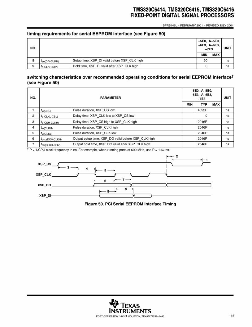
TMS320C6414, TMS320C6415, TMS320C6416FIXED-POINT DIGITAL SIGNAL PROCESSORS
SPRS146L − FEBRUARY 2001 − REVISED JULY 2004
115POST OFFICE BOX 1443 • HOUSTON, TEXAS 77251−1443
timing requirements for serial EEPROM interface (see Figure 50)
NO.
−5E0, A−5E0,−6E3, A−6E3,
−7E3 UNIT
MIN MAX
8 tsu(DIV-CLKH) Setup time, XSP_DI valid before XSP_CLK high 50 ns
9 th(CLKH-DIV) Hold time, XSP_DI valid after XSP_CLK high 0 ns
switching characteristics over recommended operating conditions for serial EEPROM interface†
(see Figure 50)
NO. PARAMETER
−5E0, A−5E0,−6E3, A−6E3,
−7E3 UNIT
MIN TYP MAX
1 tw(CSL) Pulse duration, XSP_CS low 4092P ns
2 td(CLKL-CSL) Delay time, XSP_CLK low to XSP_CS low 0 ns
3 td(CSH-CLKH) Delay time, XSP_CS high to XSP_CLK high 2046P ns
4 tw(CLKH) Pulse duration, XSP_CLK high 2046P ns
5 tw(CLKL) Pulse duration, XSP_CLK low 2046P ns
6 tosu(DOV-CLKH) Output setup time, XSP_DO valid before XSP_CLK high 2046P ns
7 toh(CLKH-DOV) Output hold time, XSP_DO valid after XSP_CLK high 2046P ns† P = 1/CPU clock frequency in ns. For example, when running parts at 600 MHz, use P = 1.67 ns.
8
76
3
2
54
1XSP_CS
XSP_CLK
XSP_DO
XSP_DI
9
Figure 50. PCI Serial EEPROM Interface Timing

TMS320C6414, TMS320C6415, TMS320C6416FIXED-POINT DIGITAL SIGNAL PROCESSORS
SPRS146L − FEBRUARY 2001 − REVISED JULY 2004
116 POST OFFICE BOX 1443 • HOUSTON, TEXAS 77251−1443
MULTICHANNEL BUFFERED SERIAL PORT (McBSP) TIMING
timing requirements for McBSP† (see Figure 51)
NO.
−5E0, A−5E0,−6E3, A−6E3,
−7E3 UNIT
MIN MAX
2 tc(CKRX) Cycle time, CLKR/X CLKR/X ext 4P or 6.67द ns
3 tw(CKRX) Pulse duration, CLKR/X high or CLKR/X low CLKR/X ext 0.5tc(CKRX) − 1# ns
5 t Setup time external FSR high before CLKR lowCLKR int 9
ns5 tsu(FRH-CKRL) Setup time, external FSR high before CLKR lowCLKR ext 1.3
ns
6 t Hold time external FSR high after CLKR lowCLKR int 6
ns6 th(CKRL-FRH) Hold time, external FSR high after CLKR lowCLKR ext 3
ns
7 t Setup time DR valid before CLKR lowCLKR int 8
ns7 tsu(DRV-CKRL) Setup time, DR valid before CLKR lowCLKR ext 0.9
ns
8 t Hold time DR valid after CLKR lowCLKR int 3
ns8 th(CKRL-DRV) Hold time, DR valid after CLKR lowCLKR ext 3.1
ns
10 t Setup time external FSX high before CLKX lowCLKX int 9
ns10 tsu(FXH-CKXL) Setup time, external FSX high before CLKX lowCLKX ext 1.3
ns
11 t Hold time external FSX high after CLKX lowCLKX int 6
ns11 th(CKXL-FXH) Hold time, external FSX high after CLKX lowCLKX ext 3
ns
† CLKRP = CLKXP = FSRP = FSXP = 0. If polarity of any of the signals is inverted, then the timing references of that signal are also inverted.‡ Minimum CLKR/X cycle times must be met, even when CLKR/X is generated by an internal clock source. Minimum CLKR/X cycle times are based
on internal logic speed; the maximum usable speed may be lower due to EDMA limitations and AC timing requirements.§ P = 1/CPU clock frequency in ns. For example, when running parts at 600 MHz, use P = 1.67 ns.¶ Use whichever value is greater.# This parameter applies to the maximum McBSP frequency. Operate serial clocks (CLKR/X) in the reasonable range of 40/60 duty cycle.

TMS320C6414, TMS320C6415, TMS320C6416FIXED-POINT DIGITAL SIGNAL PROCESSORS
SPRS146L − FEBRUARY 2001 − REVISED JULY 2004
117POST OFFICE BOX 1443 • HOUSTON, TEXAS 77251−1443
MULTICHANNEL BUFFERED SERIAL PORT (McBSP) TIMING (CONTINUED)
switching characteristics over recommended operating conditions for McBSP†‡ (see Figure 51)
NO. PARAMETER
−5E0, A−5E0,−6E3, A−6E3,
−7E3 UNIT
MIN MAX
1 td(CKSH-CKRXH)Delay time, CLKS high to CLKR/X high for internal CLKR/X generatedfrom CLKS input
1.4 10 ns
2 tc(CKRX) Cycle time, CLKR/X CLKR/X int 4P or 6.67§¶# ns
3 tw(CKRX) Pulse duration, CLKR/X high or CLKR/X low CLKR/X int C − 1|| C + 1|| ns
4 td(CKRH-FRV) Delay time, CLKR high to internal FSR valid CLKR int −2.1 3 ns
9 t Delay time CLKX high to internal FSX validCLKX int −1.7 3
ns9 td(CKXH-FXV) Delay time, CLKX high to internal FSX validCLKX ext 1.7 9
ns
12 tDisable time, DX high impedance following last data bit CLKX int −3.9 4
ns12 tdis(CKXH-DXHZ)Disable time, DX high impedance following last data bitfrom CLKX high CLKX ext 2.0 9
ns
13 t Delay time CLKX high to DX validCLKX int −3.9 + D1 4 + D2
ns13 td(CKXH-DXV) Delay time, CLKX high to DX validCLKX ext 2.0 + D1 9 + D2
ns
14 t
Delay time, FSX high to DX valid FSX int −2.3 + D1 5.6 + D2
ns14 td(FXH-DXV) ONLY applies when in datadelay 0 (XDATDLY = 00b) mode FSX ext 1.9 + D1 9 + D2
ns
† CLKRP = CLKXP = FSRP = FSXP = 0. If polarity of any of the signals is inverted, then the timing references of that signal are also inverted.‡ Minimum delay times also represent minimum output hold times.§ Minimum CLKR/X cycle times must be met, even when CLKR/X is generated by an internal clock source. Minimum CLKR/X cycle times are based
on internal logic speed; the maximum usable speed may be lower due to EDMA limitations and AC timing requirements.¶ P = 1/CPU clock frequency in ns. For example, when running parts at 600 MHz, use P = 1.67 ns.# Use whichever value is greater.|| C = H or L
S = sample rate generator input clock = 4P if CLKSM = 1 (P = 1/CPU clock frequency)= sample rate generator input clock = P_clks if CLKSM = 0 (P_clks = CLKS period)
H = CLKX high pulse width = (CLKGDV/2 + 1) * S if CLKGDV is even= (CLKGDV + 1)/2 * S if CLKGDV is odd or zero
L = CLKX low pulse width = (CLKGDV/2) * S if CLKGDV is even= (CLKGDV + 1)/2 * S if CLKGDV is odd or zero
CLKGDV should be set appropriately to ensure the McBSP bit rate does not exceed the maximum limit (see ¶ footnote above). Extra delay from CLKX high to DX valid applies only to the first data bit of a device, if and only if DXENA = 1 in SPCR.
if DXENA = 0, then D1 = D2 = 0if DXENA = 1, then D1 = 4P, D2 = 8P
Extra delay from FSX high to DX valid applies only to the first data bit of a device, if and only if DXENA = 1 in SPCR.if DXENA = 0, then D1 = D2 = 0if DXENA = 1, then D1 = 4P, D2 = 8P

TMS320C6414, TMS320C6415, TMS320C6416FIXED-POINT DIGITAL SIGNAL PROCESSORS
SPRS146L − FEBRUARY 2001 − REVISED JULY 2004
118 POST OFFICE BOX 1443 • HOUSTON, TEXAS 77251−1443
MULTICHANNEL BUFFERED SERIAL PORT (McBSP) TIMING (CONTINUED)
Bit(n-1) (n-2) (n-3)
Bit 0 Bit(n-1) (n-2) (n-3)
1412
1110
9
33
2
87
65
44
3
1
32
CLKS
CLKR
FSR (int)
FSR (ext)
DR
CLKX
FSX (int)
FSX (ext)
FSX (XDATDLY=00b)
DX
† Parameter No. 13 applies to the first data bit only when XDATDLY ≠ 0
13†
13†
Figure 51. McBSP Timing

TMS320C6414, TMS320C6415, TMS320C6416FIXED-POINT DIGITAL SIGNAL PROCESSORS
SPRS146L − FEBRUARY 2001 − REVISED JULY 2004
119POST OFFICE BOX 1443 • HOUSTON, TEXAS 77251−1443
MULTICHANNEL BUFFERED SERIAL PORT (McBSP) TIMING (CONTINUED)
timing requirements for FSR when GSYNC = 1 (see Figure 52)
NO.
−5E0, A−5E0,−6E3, A−6E3,
−7E3 UNIT
MIN MAX
1 tsu(FRH-CKSH) Setup time, FSR high before CLKS high 4 ns
2 th(CKSH-FRH) Hold time, FSR high after CLKS high 4 ns
21
CLKS
FSR external
CLKR/X (no need to resync)
CLKR/X (needs resync)
Figure 52. FSR Timing When GSYNC = 1
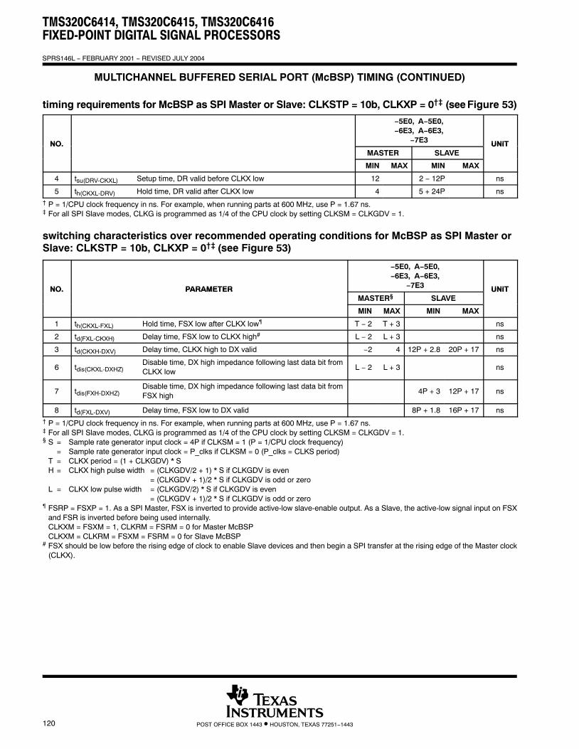
TMS320C6414, TMS320C6415, TMS320C6416FIXED-POINT DIGITAL SIGNAL PROCESSORS
SPRS146L − FEBRUARY 2001 − REVISED JULY 2004
120 POST OFFICE BOX 1443 • HOUSTON, TEXAS 77251−1443
MULTICHANNEL BUFFERED SERIAL PORT (McBSP) TIMING (CONTINUED)
timing requirements for McBSP as SPI Master or Slave: CLKSTP = 10b, CLKXP = 0†‡ (see Figure 53)
NO.
−5E0, A−5E0,−6E3, A−6E3,
−7E3 UNITNO.MASTER SLAVE
UNIT
MIN MAX MIN MAX
4 tsu(DRV-CKXL) Setup time, DR valid before CLKX low 12 2 − 12P ns
5 th(CKXL-DRV) Hold time, DR valid after CLKX low 4 5 + 24P ns† P = 1/CPU clock frequency in ns. For example, when running parts at 600 MHz, use P = 1.67 ns.‡ For all SPI Slave modes, CLKG is programmed as 1/4 of the CPU clock by setting CLKSM = CLKGDV = 1.
switching characteristics over recommended operating conditions for McBSP as SPI Master or Slave: CLKSTP = 10b, CLKXP = 0†‡ (see Figure 53)
NO. PARAMETER
−5E0, A−5E0,−6E3, A−6E3,
−7E3 UNITNO. PARAMETERMASTER§ SLAVE
UNIT
MIN MAX MIN MAX
1 th(CKXL-FXL) Hold time, FSX low after CLKX low¶ T − 2 T + 3 ns
2 td(FXL-CKXH) Delay time, FSX low to CLKX high# L − 2 L + 3 ns
3 td(CKXH-DXV) Delay time, CLKX high to DX valid −2 4 12P + 2.8 20P + 17 ns
6 tdis(CKXL-DXHZ)Disable time, DX high impedance following last data bit fromCLKX low
L − 2 L + 3 ns
7 tdis(FXH-DXHZ)Disable time, DX high impedance following last data bit fromFSX high
4P + 3 12P + 17 ns
8 td(FXL-DXV) Delay time, FSX low to DX valid 8P + 1.8 16P + 17 ns† P = 1/CPU clock frequency in ns. For example, when running parts at 600 MHz, use P = 1.67 ns.‡ For all SPI Slave modes, CLKG is programmed as 1/4 of the CPU clock by setting CLKSM = CLKGDV = 1.§ S = Sample rate generator input clock = 4P if CLKSM = 1 (P = 1/CPU clock frequency)
= Sample rate generator input clock = P_clks if CLKSM = 0 (P_clks = CLKS period)T = CLKX period = (1 + CLKGDV) * SH = CLKX high pulse width = (CLKGDV/2 + 1) * S if CLKGDV is even
= (CLKGDV + 1)/2 * S if CLKGDV is odd or zeroL = CLKX low pulse width = (CLKGDV/2) * S if CLKGDV is even
= (CLKGDV + 1)/2 * S if CLKGDV is odd or zero¶ FSRP = FSXP = 1. As a SPI Master, FSX is inverted to provide active-low slave-enable output. As a Slave, the active-low signal input on FSX
and FSR is inverted before being used internally.CLKXM = FSXM = 1, CLKRM = FSRM = 0 for Master McBSPCLKXM = CLKRM = FSXM = FSRM = 0 for Slave McBSP
# FSX should be low before the rising edge of clock to enable Slave devices and then begin a SPI transfer at the rising edge of the Master clock(CLKX).

TMS320C6414, TMS320C6415, TMS320C6416FIXED-POINT DIGITAL SIGNAL PROCESSORS
SPRS146L − FEBRUARY 2001 − REVISED JULY 2004
121POST OFFICE BOX 1443 • HOUSTON, TEXAS 77251−1443
MULTICHANNEL BUFFERED SERIAL PORT (McBSP) TIMING (CONTINUED)
Bit 0 Bit(n-1) (n-2) (n-3) (n-4)
Bit 0 Bit(n-1) (n-2) (n-3) (n-4)5
4
387
6
21
CLKX
FSX
DX
DR
Figure 53. McBSP Timing as SPI Master or Slave: CLKSTP = 10b, CLKXP = 0
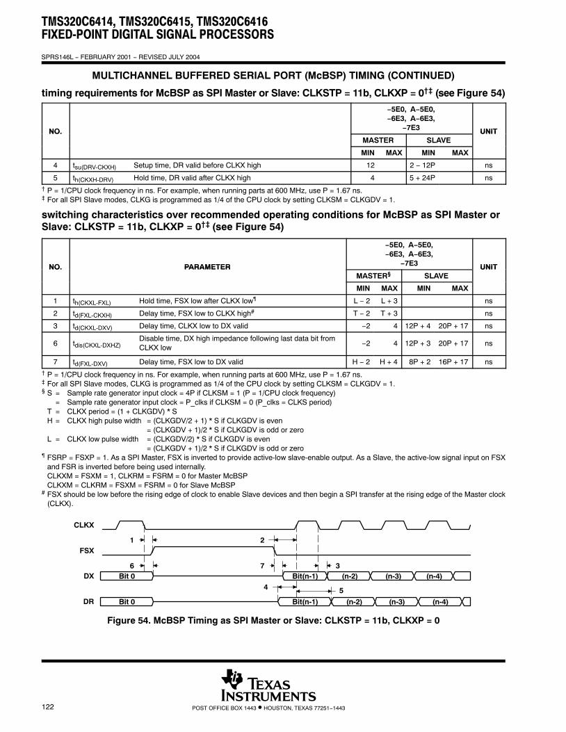
TMS320C6414, TMS320C6415, TMS320C6416FIXED-POINT DIGITAL SIGNAL PROCESSORS
SPRS146L − FEBRUARY 2001 − REVISED JULY 2004
122 POST OFFICE BOX 1443 • HOUSTON, TEXAS 77251−1443
MULTICHANNEL BUFFERED SERIAL PORT (McBSP) TIMING (CONTINUED)
timing requirements for McBSP as SPI Master or Slave: CLKSTP = 11b, CLKXP = 0†‡ (see Figure 54)
NO.
−5E0, A−5E0,−6E3, A−6E3,
−7E3 UNITNO.MASTER SLAVE
UNIT
MIN MAX MIN MAX
4 tsu(DRV-CKXH) Setup time, DR valid before CLKX high 12 2 − 12P ns
5 th(CKXH-DRV) Hold time, DR valid after CLKX high 4 5 + 24P ns† P = 1/CPU clock frequency in ns. For example, when running parts at 600 MHz, use P = 1.67 ns.‡ For all SPI Slave modes, CLKG is programmed as 1/4 of the CPU clock by setting CLKSM = CLKGDV = 1.
switching characteristics over recommended operating conditions for McBSP as SPI Master or Slave: CLKSTP = 11b, CLKXP = 0†‡ (see Figure 54)
NO. PARAMETER
−5E0, A−5E0,−6E3, A−6E3,
−7E3 UNITNO. PARAMETERMASTER§ SLAVE
UNIT
MIN MAX MIN MAX
1 th(CKXL-FXL) Hold time, FSX low after CLKX low¶ L − 2 L + 3 ns
2 td(FXL-CKXH) Delay time, FSX low to CLKX high# T − 2 T + 3 ns
3 td(CKXL-DXV) Delay time, CLKX low to DX valid −2 4 12P + 4 20P + 17 ns
6 tdis(CKXL-DXHZ)Disable time, DX high impedance following last data bit fromCLKX low
−2 4 12P + 3 20P + 17 ns
7 td(FXL-DXV) Delay time, FSX low to DX valid H − 2 H + 4 8P + 2 16P + 17 ns† P = 1/CPU clock frequency in ns. For example, when running parts at 600 MHz, use P = 1.67 ns.‡ For all SPI Slave modes, CLKG is programmed as 1/4 of the CPU clock by setting CLKSM = CLKGDV = 1.§ S = Sample rate generator input clock = 4P if CLKSM = 1 (P = 1/CPU clock frequency)
= Sample rate generator input clock = P_clks if CLKSM = 0 (P_clks = CLKS period)T = CLKX period = (1 + CLKGDV) * SH = CLKX high pulse width = (CLKGDV/2 + 1) * S if CLKGDV is even
= (CLKGDV + 1)/2 * S if CLKGDV is odd or zeroL = CLKX low pulse width = (CLKGDV/2) * S if CLKGDV is even
= (CLKGDV + 1)/2 * S if CLKGDV is odd or zero¶ FSRP = FSXP = 1. As a SPI Master, FSX is inverted to provide active-low slave-enable output. As a Slave, the active-low signal input on FSX
and FSR is inverted before being used internally.CLKXM = FSXM = 1, CLKRM = FSRM = 0 for Master McBSPCLKXM = CLKRM = FSXM = FSRM = 0 for Slave McBSP
# FSX should be low before the rising edge of clock to enable Slave devices and then begin a SPI transfer at the rising edge of the Master clock(CLKX).
Bit 0 Bit(n-1) (n-2) (n-3) (n-4)
Bit 0 Bit(n-1) (n-2) (n-3) (n-4)
4
376
21
CLKX
FSX
DX
DR
5
Figure 54. McBSP Timing as SPI Master or Slave: CLKSTP = 11b, CLKXP = 0
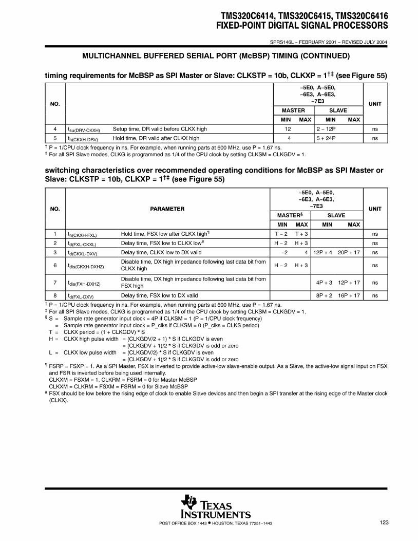
TMS320C6414, TMS320C6415, TMS320C6416FIXED-POINT DIGITAL SIGNAL PROCESSORS
SPRS146L − FEBRUARY 2001 − REVISED JULY 2004
123POST OFFICE BOX 1443 • HOUSTON, TEXAS 77251−1443
MULTICHANNEL BUFFERED SERIAL PORT (McBSP) TIMING (CONTINUED)
timing requirements for McBSP as SPI Master or Slave: CLKSTP = 10b, CLKXP = 1†‡ (see Figure 55)
NO.
−5E0, A−5E0,−6E3, A−6E3,
−7E3 UNITNO.MASTER SLAVE
UNIT
MIN MAX MIN MAX
4 tsu(DRV-CKXH) Setup time, DR valid before CLKX high 12 2 − 12P ns
5 th(CKXH-DRV) Hold time, DR valid after CLKX high 4 5 + 24P ns† P = 1/CPU clock frequency in ns. For example, when running parts at 600 MHz, use P = 1.67 ns.‡ For all SPI Slave modes, CLKG is programmed as 1/4 of the CPU clock by setting CLKSM = CLKGDV = 1.
switching characteristics over recommended operating conditions for McBSP as SPI Master or Slave: CLKSTP = 10b, CLKXP = 1†‡ (see Figure 55)
NO. PARAMETER
−5E0, A−5E0,−6E3, A−6E3,
−7E3 UNITNO. PARAMETERMASTER§ SLAVE
UNIT
MIN MAX MIN MAX
1 th(CKXH-FXL) Hold time, FSX low after CLKX high¶ T − 2 T + 3 ns
2 td(FXL-CKXL) Delay time, FSX low to CLKX low# H − 2 H + 3 ns
3 td(CKXL-DXV) Delay time, CLKX low to DX valid −2 4 12P + 4 20P + 17 ns
6 tdis(CKXH-DXHZ)Disable time, DX high impedance following last data bit fromCLKX high
H − 2 H + 3 ns
7 tdis(FXH-DXHZ)Disable time, DX high impedance following last data bit fromFSX high
4P + 3 12P + 17 ns
8 td(FXL-DXV) Delay time, FSX low to DX valid 8P + 2 16P + 17 ns† P = 1/CPU clock frequency in ns. For example, when running parts at 600 MHz, use P = 1.67 ns.‡ For all SPI Slave modes, CLKG is programmed as 1/4 of the CPU clock by setting CLKSM = CLKGDV = 1.§ S = Sample rate generator input clock = 4P if CLKSM = 1 (P = 1/CPU clock frequency)
= Sample rate generator input clock = P_clks if CLKSM = 0 (P_clks = CLKS period)T = CLKX period = (1 + CLKGDV) * SH = CLKX high pulse width = (CLKGDV/2 + 1) * S if CLKGDV is even
= (CLKGDV + 1)/2 * S if CLKGDV is odd or zeroL = CLKX low pulse width = (CLKGDV/2) * S if CLKGDV is even
= (CLKGDV + 1)/2 * S if CLKGDV is odd or zero¶ FSRP = FSXP = 1. As a SPI Master, FSX is inverted to provide active-low slave-enable output. As a Slave, the active-low signal input on FSX
and FSR is inverted before being used internally.CLKXM = FSXM = 1, CLKRM = FSRM = 0 for Master McBSPCLKXM = CLKRM = FSXM = FSRM = 0 for Slave McBSP
# FSX should be low before the rising edge of clock to enable Slave devices and then begin a SPI transfer at the rising edge of the Master clock(CLKX).

TMS320C6414, TMS320C6415, TMS320C6416FIXED-POINT DIGITAL SIGNAL PROCESSORS
SPRS146L − FEBRUARY 2001 − REVISED JULY 2004
124 POST OFFICE BOX 1443 • HOUSTON, TEXAS 77251−1443
MULTICHANNEL BUFFERED SERIAL PORT (McBSP) TIMING (CONTINUED)
Bit 0 Bit(n-1) (n-2) (n-3) (n-4)
Bit 0 Bit(n-1) (n-2) (n-3) (n-4)54
387
6
21
CLKX
FSX
DX
DR
Figure 55. McBSP Timing as SPI Master or Slave: CLKSTP = 10b, CLKXP = 1
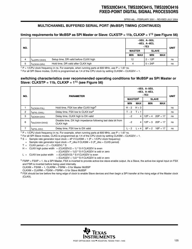
TMS320C6414, TMS320C6415, TMS320C6416FIXED-POINT DIGITAL SIGNAL PROCESSORS
SPRS146L − FEBRUARY 2001 − REVISED JULY 2004
125POST OFFICE BOX 1443 • HOUSTON, TEXAS 77251−1443
MULTICHANNEL BUFFERED SERIAL PORT (McBSP) TIMING (CONTINUED)
timing requirements for McBSP as SPI Master or Slave: CLKSTP = 11b, CLKXP = 1†‡ (see Figure 56)
NO.
−5E0, A−5E0,−6E3, A−6E3,
−7E3 UNITNO.MASTER SLAVE
UNIT
MIN MAX MIN MAX
4 tsu(DRV-CKXH) Setup time, DR valid before CLKX high 12 2 − 12P ns
5 th(CKXH-DRV) Hold time, DR valid after CLKX high 4 5 + 24P ns† P = 1/CPU clock frequency in ns. For example, when running parts at 600 MHz, use P = 1.67 ns.‡ For all SPI Slave modes, CLKG is programmed as 1/4 of the CPU clock by setting CLKSM = CLKGDV = 1.
switching characteristics over recommended operating conditions for McBSP as SPI Master or Slave: CLKSTP = 11b, CLKXP = 1†‡ (see Figure 56)
NO. PARAMETER
−5E0, A−5E0,−6E3, A−6E3,
−7E3 UNITNO. PARAMETERMASTER§ SLAVE
UNIT
MIN MAX MIN MAX
1 th(CKXH-FXL) Hold time, FSX low after CLKX high¶ H − 2 H + 3 ns
2 td(FXL-CKXL) Delay time, FSX low to CLKX low# T − 2 T + 1 ns
3 td(CKXH-DXV) Delay time, CLKX high to DX valid −2 4 12P + 4 20P + 17 ns
6 tdis(CKXH-DXHZ)Disable time, DX high impedance following last data bit fromCLKX high
−2 4 12P + 3 20P + 17 ns
7 td(FXL-DXV) Delay time, FSX low to DX valid L − 2 L + 4 8P + 2 16P + 17 ns† P = 1/CPU clock frequency in ns. For example, when running parts at 600 MHz, use P = 1.67 ns.‡ For all SPI Slave modes, CLKG is programmed as 1/4 of the CPU clock by setting CLKSM = CLKGDV = 1.§ S = Sample rate generator input clock = 4P if CLKSM = 1 (P = 1/CPU clock frequency)
= Sample rate generator input clock = P_clks if CLKSM = 0 (P_clks = CLKS period)T = CLKX period = (1 + CLKGDV) * SH = CLKX high pulse width = (CLKGDV/2 + 1) * S if CLKGDV is even
= (CLKGDV + 1)/2 * S if CLKGDV is odd or zeroL = CLKX low pulse width = (CLKGDV/2) * S if CLKGDV is even
= (CLKGDV + 1)/2 * S if CLKGDV is odd or zero¶ FSRP = FSXP = 1. As a SPI Master, FSX is inverted to provide active-low slave-enable output. As a Slave, the active-low signal input on FSX
and FSR is inverted before being used internally.CLKXM = FSXM = 1, CLKRM = FSRM = 0 for Master McBSPCLKXM = CLKRM = FSXM = FSRM = 0 for Slave McBSP
# FSX should be low before the rising edge of clock to enable Slave devices and then begin a SPI transfer at the rising edge of the Master clock(CLKX).

TMS320C6414, TMS320C6415, TMS320C6416FIXED-POINT DIGITAL SIGNAL PROCESSORS
SPRS146L − FEBRUARY 2001 − REVISED JULY 2004
126 POST OFFICE BOX 1443 • HOUSTON, TEXAS 77251−1443
MULTICHANNEL BUFFERED SERIAL PORT (McBSP) TIMING (CONTINUED)
Bit 0 Bit(n-1) (n-2) (n-3) (n-4)
Bit 0 Bit(n-1) (n-2) (n-3) (n-4)54
376
21
CLKX
FSX
DX
DR
Figure 56. McBSP Timing as SPI Master or Slave: CLKSTP = 11b, CLKXP = 1

TMS320C6414, TMS320C6415, TMS320C6416FIXED-POINT DIGITAL SIGNAL PROCESSORS
SPRS146L − FEBRUARY 2001 − REVISED JULY 2004
127POST OFFICE BOX 1443 • HOUSTON, TEXAS 77251−1443
UTOPIA SLAVE TIMING [C6415 AND C6416 ONLY]
timing requirements for UXCLK† (see Figure 57)
NO.
−5E0, A−5E0,−6E3, A−6E3,
−7E3 UNIT
MIN MAX
1 tc(UXCK) Cycle time, UXCLK 20 ns
2 tw(UXCKH) Pulse duration, UXCLK high 0.4tc(UXCK) 0.6tc(UXCK) ns
3 tw(UXCKL) Pulse duration, UXCLK low 0.4tc(UXCK) 0.6tc(UXCK) ns
4 tt(UXCK) Transition time, UXCLK 2 ns† The reference points for the rise and fall transitions are measured at VIL MAX and VIH MIN.
UXCLK
1
2
3
4
4
Figure 57. UXCLK Timing
timing requirements for URCLK† (see Figure 58)
NO.
−5E0, A−5E0,−6E3, A−6E3,
−7E3 UNIT
MIN MAX
1 tc(URCK) Cycle time, URCLK 20 ns
2 tw(URCKH) Pulse duration, URCLK high 0.4tc(URCK) 0.6tc(URCK) ns
3 tw(URCKL) Pulse duration, URCLK low 0.4tc(URCK) 0.6tc(URCK) ns
4 tt(URCK) Transition time, URCLK 2 ns† The reference points for the rise and fall transitions are measured at VIL MAX and VIH MIN.
URCLK
1
2
3
4
4
Figure 58. URCLK Timing

TMS320C6414, TMS320C6415, TMS320C6416FIXED-POINT DIGITAL SIGNAL PROCESSORS
SPRS146L − FEBRUARY 2001 − REVISED JULY 2004
128 POST OFFICE BOX 1443 • HOUSTON, TEXAS 77251−1443
UTOPIA SLAVE TIMING [C6415 AND C6416 ONLY] (CONTINUED)
timing requirements for UTOPIA Slave transmit (see Figure 59)
NO.
−5E0, A−5E0,−6E3, A−6E3,
−7E3 UNIT
MIN MAX
2 tsu(UXAV-UXCH) Setup time, UXADDR valid before UXCLK high 4 ns
3 th(UXCH-UXAV) Hold time, UXADDR valid after UXCLK high 1 ns
8 tsu(UXENBL-UXCH) Setup time, UXENB low before UXCLK high 4 ns
9 th(UXCH-UXENBL) Hold time, UXENB low after UXCLK high 1 ns
switching characteristics over recommended operating conditions for UTOPIA Slave transmit(see Figure 59)
NO. PARAMETER
−5E0, A−5E0,−6E3, A−6E3,
−7E3 UNIT
MIN MAX
1 td(UXCH-UXDV) Delay time, UXCLK high to UXDATA valid 3 12 ns
4 td(UXCH-UXCLAV) Delay time, UXCLK high to UXCLAV driven active value 3 12 ns
5 td(UXCH-UXCLAVL) Delay time, UXCLK high to UXCLAV driven inactive low 3 12 ns
6 td(UXCH-UXCLAVHZ) Delay time, UXCLK high to UXCLAV going Hi-Z 9 18.5 ns
7 tw(UXCLAVL-UXCLAVHZ) Pulse duration (low), UXCLAV low to UXCLAV Hi-Z 3 ns
10 td(UXCH-UXSV) Delay time, UXCLK high to UXSOC valid 3 12 ns
P47 P48 H1
N 0x1F N 0x1F N + 1 0x1F
N N
10
8
4
32
1
UXCLK
UXDATA[7:0]
UXADDR[4:0]
UXCLAV
UXENB
UXSOC
9
P46P45
0 x1F
The UTOPIA Slave module has signals that are middle-level signals indicating a high-impedance state (i.e., the UXCLAV andUXSOC signals).
†
5
67
Figure 59. UTOPIA Slave Transmit Timing†

TMS320C6414, TMS320C6415, TMS320C6416FIXED-POINT DIGITAL SIGNAL PROCESSORS
SPRS146L − FEBRUARY 2001 − REVISED JULY 2004
129POST OFFICE BOX 1443 • HOUSTON, TEXAS 77251−1443
UTOPIA SLAVE TIMING [C6415 AND C6416 ONLY] (CONTINUED)timing requirements for UTOPIA Slave receive (see Figure 60)
NO.
−5E0, A−5E0,−6E3, A−6E3,
−7E3 UNIT
MIN MAX
1 tsu(URDV-URCH) Setup time, URDATA valid before URCLK high 4 ns
2 th(URCH-URDV) Hold time, URDATA valid after URCLK high 1 ns
3 tsu(URAV-URCH) Setup time, URADDR valid before URCLK high 4 ns
4 th(URCH-URAV) Hold time, URADDR valid after URCLK high 1 ns
9 tsu(URENBL-URCH) Setup time, URENB low before URCLK high 4 ns
10 th(URCH-URENBL) Hold time, URENB low after URCLK high 1 ns
11 tsu(URSH-URCH) Setup time, URSOC high before URCLK high 4 ns
12 th(URCH-URSH) Hold time, URSOC high after URCLK high 1 ns
switching characteristics over recommended operating conditions for UTOPIA Slave receive(see Figure 60)
NO. PARAMETER
−5E0, A−5E0,−6E3, A−6E3,
−7E3 UNIT
MIN MAX
5 td(URCH-URCLAV) Delay time, URCLK high to URCLAV driven active value 3 12 ns
6 td(URCH-URCLAVL) Delay time, URCLK high to URCLAV driven inactive low 3 12 ns
7 td(URCH-URCLAVHZ) Delay time, URCLK high to URCLAV going Hi-Z 9 18.5 ns
8 tw(URCLAVL-URCLAVHZ) Pulse duration (low), URCLAV low to URCLAV Hi-Z 3 ns
P48 H1 H2 H3
N 0x1F N+1 0x1F N+2 0x1F
N N+1 N+2
1211
910
5
43
21
URCLK
URDATA[7:0]
URADDR[4:0]
URCLAV
URENB
URSOC
The UTOPIA Slave module has signals that are middle-level signals indicating a high-impedance state (i.e., the URCLAV andURSOC signals).
†
86
7
Figure 60. UTOPIA Slave Receive Timing†
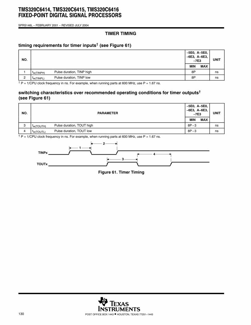
TMS320C6414, TMS320C6415, TMS320C6416FIXED-POINT DIGITAL SIGNAL PROCESSORS
SPRS146L − FEBRUARY 2001 − REVISED JULY 2004
130 POST OFFICE BOX 1443 • HOUSTON, TEXAS 77251−1443
TIMER TIMING
timing requirements for timer inputs† (see Figure 61)
NO.
−5E0, A−5E0,−6E3, A−6E3,
−7E3 UNIT
MIN MAX
1 tw(TINPH) Pulse duration, TINP high 8P ns
2 tw(TINPL) Pulse duration, TINP low 8P ns† P = 1/CPU clock frequency in ns. For example, when running parts at 600 MHz, use P = 1.67 ns.
switching characteristics over recommended operating conditions for timer outputs† (see Figure 61)
NO. PARAMETER
−5E0, A−5E0,−6E3, A−6E3,
−7E3 UNIT
MIN MAX
3 tw(TOUTH) Pulse duration, TOUT high 8P−3 ns
4 tw(TOUTL) Pulse duration, TOUT low 8P−3 ns† P = 1/CPU clock frequency in ns. For example, when running parts at 600 MHz, use P = 1.67 ns.
TINPx
TOUTx
4
3
21
Figure 61. Timer Timing

TMS320C6414, TMS320C6415, TMS320C6416FIXED-POINT DIGITAL SIGNAL PROCESSORS
SPRS146L − FEBRUARY 2001 − REVISED JULY 2004
131POST OFFICE BOX 1443 • HOUSTON, TEXAS 77251−1443
GENERAL-PURPOSE INPUT/OUTPUT (GPIO) PORT TIMING
timing requirements for GPIO inputs†‡ (see Figure 62)
NO.
−5E0, A−5E0,−6E3, A−6E3,
−7E3 UNIT
MIN MAX
1 tw(GPIH) Pulse duration, GPIx high 8P ns
2 tw(GPIL) Pulse duration, GPIx low 8P ns† P = 1/CPU clock frequency in ns. For example, when running parts at 600 MHz, use P = 1.67 ns.‡ The pulse width given is sufficient to generate a CPU interrupt or an EDMA event. However, if a user wants to have the DSP recognize the GPIx
changes through software polling of the GPIO register, the GPIx duration must be extended to at least 12P to allow the DSP enough time to accessthe GPIO register through the CFGBUS.
switching characteristics over recommended operating conditions for GPIO outputs† (see Figure 62)
NO. PARAMETER
−5E0, A−5E0,−6E3, A−6E3,
−7E3 UNIT
MIN MAX
3 tw(GPOH) Pulse duration, GPOx high 24P − 8‡ ns
4 tw(GPOL) Pulse duration, GPOx low 24P − 8‡ ns† P = 1/CPU clock frequency in ns. For example, when running parts at 600 MHz, use P = 1.67 ns.‡ This parameter value should not be used as a maximum performance specification. Actual performance of back-to-back accesses of the GPIO
is dependent upon internal bus activity.
GPIx
GPOx
4
3
21
Figure 62. GPIO Port Timing
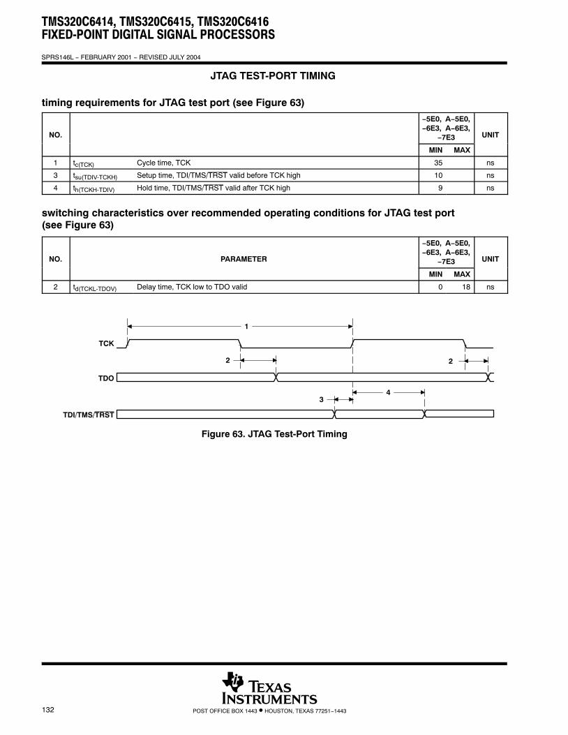
TMS320C6414, TMS320C6415, TMS320C6416FIXED-POINT DIGITAL SIGNAL PROCESSORS
SPRS146L − FEBRUARY 2001 − REVISED JULY 2004
132 POST OFFICE BOX 1443 • HOUSTON, TEXAS 77251−1443
JTAG TEST-PORT TIMING
timing requirements for JTAG test port (see Figure 63)
NO.
−5E0, A−5E0,−6E3, A−6E3,
−7E3 UNIT
MIN MAX
1 tc(TCK) Cycle time, TCK 35 ns
3 tsu(TDIV-TCKH) Setup time, TDI/TMS/TRST valid before TCK high 10 ns
4 th(TCKH-TDIV) Hold time, TDI/TMS/TRST valid after TCK high 9 ns
switching characteristics over recommended operating conditions for JTAG test port (see Figure 63)
NO. PARAMETER
−5E0, A−5E0,−6E3, A−6E3,
−7E3 UNIT
MIN MAX
2 td(TCKL-TDOV) Delay time, TCK low to TDO valid 0 18 ns
TCK
TDO
TDI/TMS/TRST
1
2
34
2
Figure 63. JTAG Test-Port Timing

TMS320C6414, TMS320C6415, TMS320C6416FIXED-POINT DIGITAL SIGNAL PROCESSORS
SPRS146L − FEBRUARY 2001 − REVISED JULY 2004
133POST OFFICE BOX 1443 • HOUSTON, TEXAS 77251−1443
MECHANICAL DATA FOR C6414, C6415, AND C6416
The following table(s) show the thermal resistance characteristics for the PBGA — GLZ, ZLZ and CLZmechanical packages.
thermal resistance characteristics (S-PBGA package) [GLZ]
NO. Air Flow (m/s†) °C/W°C/W
(with Heat Sink‡)
1 RΘJC Junction-to-case N/A 1.55 1.0
2 RΘJB Junction-to-board N/A 9.1 9.0
3 RΘJA Junction-to-free air 0.00 17.9 13.8
4 RΘJA Junction-to-free air 0.5 15.02 8.95
5 RΘJA Junction-to-free air 1.0 13.4 7.35
6 RΘJA Junction-to-free air 2.00 11.89 6.46
7 PsiJT Junction-to-package top N/A 0.5 0.5
8 PsiJB Junction-to-board N/A 7.4 7.4† m/s = meters per second‡ These thermal resistance numbers were modeled using a heat sink, part number 374024B00035, manufactured by AAVID Thermalloy. AAVID
Thermalloy also manufactures a similar epoxy-mounted heat sink, part number 374024B00000. When operating at 720 MHz, a heat sink shouldbe used to reduce the thermal resistance characteristics of the package. TI recommends a passive, laminar heat sink, similar to the part numbersmentioned above.
thermal resistance characteristics (S-PBGA package) [ZLZ]
NO. Air Flow (m/s†) °C/W°C/W
(with Heat Sink‡)
1 RΘJC Junction-to-case N/A 1.55 1.0
2 RΘJB Junction-to-board N/A 9.1 9.0
3 RΘJA Junction-to-free air 0.00 17.9 13.8
4 RΘJA Junction-to-free air 0.5 15.02 8.95
5 RΘJA Junction-to-free air 1.0 13.4 7.35
6 RΘJA Junction-to-free air 2.00 11.89 6.46
7 PsiJT Junction-to-package top N/A 0.5 0.5
8 PsiJB Junction-to-board N/A 7.4 7.4† m/s = meters per second‡ These thermal resistance numbers were modeled using a heat sink, part number 374024B00035, manufactured by AAVID Thermalloy. AAVID
Thermalloy also manufactures a similar epoxy-mounted heat sink, part number 374024B00000. When operating at 720 MHz, a heat sink shouldbe used to reduce the thermal resistance characteristics of the package. TI recommends a passive, laminar heat sink, similar to the part numbersmentioned above.

TMS320C6414, TMS320C6415, TMS320C6416FIXED-POINT DIGITAL SIGNAL PROCESSORS
SPRS146L − FEBRUARY 2001 − REVISED JULY 2004
134 POST OFFICE BOX 1443 • HOUSTON, TEXAS 77251−1443
thermal resistance characteristics (S-PBGA package) [CLZ]
NO. Air Flow (m/s†) °C/W°C/W
(with Heat Sink‡)
1 RΘJC Junction-to-case N/A 1.55 1.0
2 RΘJB Junction-to-board N/A 9.1 9.0
3 RΘJA Junction-to-free air 0.00 17.9 13.8
4 RΘJA Junction-to-free air 0.5 15.02 8.95
5 RΘJA Junction-to-free air 1.0 13.4 7.35
6 RΘJA Junction-to-free air 2.00 11.89 6.46
7 PsiJT Junction-to-package top N/A 0.5 0.5
8 PsiJB Junction-to-board N/A 7.4 7.4† m/s = meters per second‡ These thermal resistance numbers were modeled using a heat sink, part number 374024B00035, manufactured by AAVID Thermalloy. AAVID
Thermalloy also manufactures a similar epoxy-mounted heat sink, part number 374024B00000. When operating at 720 MHz, a heat sink shouldbe used to reduce the thermal resistance characteristics of the package. TI recommends a passive, laminar heat sink, similar to the part numbersmentioned above.

TMS320C6414, TMS320C6415, TMS320C6416FIXED-POINT DIGITAL SIGNAL PROCESSORS
SPRS146L − FEBRUARY 2001 − REVISED JULY 2004
135POST OFFICE BOX 1443 • HOUSTON, TEXAS 77251−1443
packaging information
The following packaging information and addendum reflect the most current released data available for thedesignated device(s). This data is subject to change without notice and without revision of this document.

PACKAGE OPTION ADDENDUM
www.ti.com 7-Jul-2018
Addendum-Page 1
PACKAGING INFORMATION
Orderable Device Status(1)
Package Type PackageDrawing
Pins PackageQty
Eco Plan(2)
Lead/Ball Finish(6)
MSL Peak Temp(3)
Op Temp (°C) Device Marking(4/5)
Samples
TMS32C6414EGLZ5E0 ACTIVE FCBGA GLZ 532 60 TBD SNPB Level-4-220C-72 HR TMS320C6414GLZ@2003 TI5E0
TMS32C6414EGLZ6E3 ACTIVE FCBGA GLZ 532 60 TBD SNPB Level-4-220C-72 HR TMS320C6414GLZ@2003 TI
TMS32C6414EGLZ7E3 ACTIVE FCBGA GLZ 532 60 TBD SNPB Level-4-220C-72 HR TMS320C6414GLZ@2003 TI7E3
TMS32C6414EGLZA5E0 ACTIVE FCBGA GLZ 532 60 TBD SNPB Level-4-220C-72 HR TMS320C6414GLZ@2003 TIA5E0
TMS32C6414EGLZA6E3 ACTIVE FCBGA GLZ 532 60 TBD SNPB Level-4-220C-72 HR TMS320C6414GLZ@2003 TIA6E3
TMS32C6414EZLZ5E0 ACTIVE FCBGA ZLZ 532 60 Pb-Free (RoHSExempt)
SNAGCU Level-4-260C-72HR TMS320C6414ZLZ@2003 TI5E0
TMS32C6414EZLZ6E3 ACTIVE FCBGA ZLZ 532 60 Pb-Free (RoHSExempt)
SNAGCU Level-4-260C-72HR TMS320C6414ZLZ@2003 TI
TMS32C6414EZLZ7E3 ACTIVE FCBGA ZLZ 532 60 Pb-Free (RoHSExempt)
SNAGCU Level-4-260C-72HR TMS320C6414ZLZ@2003 TI7E3
TMS32C6414EZLZA5E0 ACTIVE FCBGA ZLZ 532 60 Pb-Free (RoHSExempt)
SNAGCU Level-4-260C-72HR TMS320C6414ZLZ@2003 TIA5E0
TMS32C6414EZLZA6E3 ACTIVE FCBGA ZLZ 532 60 Pb-Free (RoHSExempt)
SNAGCU Level-4-260C-72HR TMS320C6414ZLZ@2003 TIA6E3
TMS32C6415EGLZ5E0 ACTIVE FCBGA GLZ 532 60 TBD SNPB Level-4-220C-72 HR TMS320C6415GLZ@2003 TI5E0
TMS32C6415EGLZ6E3 ACTIVE FCBGA GLZ 532 60 TBD SNPB Level-4-220C-72 HR TMS320C6415GLZ@2003 TI
TMS32C6415EGLZA5E0 ACTIVE FCBGA GLZ 532 60 TBD SNPB Level-4-220C-72 HR TMS320C6415GLZ@2003 TIA5E0

PACKAGE OPTION ADDENDUM
www.ti.com 7-Jul-2018
Addendum-Page 2
Orderable Device Status(1)
Package Type PackageDrawing
Pins PackageQty
Eco Plan(2)
Lead/Ball Finish(6)
MSL Peak Temp(3)
Op Temp (°C) Device Marking(4/5)
Samples
TMS32C6415EGLZA6E3 ACTIVE FCBGA GLZ 532 60 TBD SNPB Level-4-220C-72 HR TMS320C6415GLZ@2003 TIA6E3
TMS32C6415EZLZ5E0 ACTIVE FCBGA ZLZ 532 60 Pb-Free (RoHSExempt)
SNAGCU Level-4-260C-72HR TMS320C6415ZLZ@2003 TI5E0
TMS32C6415EZLZ6E3 ACTIVE FCBGA ZLZ 532 60 Pb-Free (RoHSExempt)
SNAGCU Level-4-260C-72HR TMS320C6415ZLZ@2003 TI
TMS32C6415EZLZ7E3 ACTIVE FCBGA ZLZ 532 60 Pb-Free (RoHSExempt)
SNAGCU Level-4-260C-72HR TMS320C6415ZLZ@2003 TI7E3
TMS32C6415EZLZA5E0 ACTIVE FCBGA ZLZ 532 60 Pb-Free (RoHSExempt)
SNAGCU Level-4-260C-72HR TMS320C6415ZLZ@2003 TIA5E0
TMS32C6416EGLZ5E0 ACTIVE FCBGA GLZ 532 60 TBD SNPB Level-4-220C-72 HR TMS320C6416GLZ@2003 TI5E0
TMS32C6416EGLZ6E3 ACTIVE FCBGA GLZ 532 60 TBD SNPB Level-4-220C-72 HR TMS320C6416GLZ@2003 TI
TMS32C6416EGLZ7E3 ACTIVE FCBGA GLZ 532 60 TBD SNPB Level-4-220C-72 HR TMS320C6416GLZ@2003 TI7E3
TMS32C6416EGLZA5E0 ACTIVE FCBGA GLZ 532 60 TBD SNPB Level-4-220C-72 HR TMS320C6416GLZ@2003 TIA5E0
TMS32C6416EGLZA6E3 ACTIVE FCBGA GLZ 532 60 TBD SNPB Level-4-220C-72 HR TMS320C6416GLZ@2003 TIA6E3
TMS32C6416EZLZ5E0 ACTIVE FCBGA ZLZ 532 60 Pb-Free (RoHSExempt)
SNAGCU Level-4-260C-72HR TMS320C6416ZLZ@2003 TI5E0
TMS32C6416EZLZ6E3 ACTIVE FCBGA ZLZ 532 60 Pb-Free (RoHSExempt)
SNAGCU Level-4-260C-72HR TMS320C6416ZLZ@2003 TI
TMS32C6416EZLZA6E3 ACTIVE FCBGA ZLZ 532 60 Pb-Free (RoHSExempt)
SNAGCU Level-4-260C-72HR TMS320C6416ZLZ@2003 TIA6E3
(1) The marketing status values are defined as follows:
PACKAGE OPTION ADDENDUM
www.ti.com 7-Jul-2018
Addendum-Page 3
ACTIVE: Product device recommended for new designs.LIFEBUY: TI has announced that the device will be discontinued, and a lifetime-buy period is in effect.NRND: Not recommended for new designs. Device is in production to support existing customers, but TI does not recommend using this part in a new design.PREVIEW: Device has been announced but is not in production. Samples may or may not be available.OBSOLETE: TI has discontinued the production of the device.
(2) RoHS: TI defines "RoHS" to mean semiconductor products that are compliant with the current EU RoHS requirements for all 10 RoHS substances, including the requirement that RoHS substancedo not exceed 0.1% by weight in homogeneous materials. Where designed to be soldered at high temperatures, "RoHS" products are suitable for use in specified lead-free processes. TI mayreference these types of products as "Pb-Free".RoHS Exempt: TI defines "RoHS Exempt" to mean products that contain lead but are compliant with EU RoHS pursuant to a specific EU RoHS exemption.Green: TI defines "Green" to mean the content of Chlorine (Cl) and Bromine (Br) based flame retardants meet JS709B low halogen requirements of <=1000ppm threshold. Antimony trioxide basedflame retardants must also meet the <=1000ppm threshold requirement.
(3) MSL, Peak Temp. - The Moisture Sensitivity Level rating according to the JEDEC industry standard classifications, and peak solder temperature.
(4) There may be additional marking, which relates to the logo, the lot trace code information, or the environmental category on the device.
(5) Multiple Device Markings will be inside parentheses. Only one Device Marking contained in parentheses and separated by a "~" will appear on a device. If a line is indented then it is a continuationof the previous line and the two combined represent the entire Device Marking for that device.
(6) Lead/Ball Finish - Orderable Devices may have multiple material finish options. Finish options are separated by a vertical ruled line. Lead/Ball Finish values may wrap to two lines if the finishvalue exceeds the maximum column width.
Important Information and Disclaimer:The information provided on this page represents TI's knowledge and belief as of the date that it is provided. TI bases its knowledge and belief on informationprovided by third parties, and makes no representation or warranty as to the accuracy of such information. Efforts are underway to better integrate information from third parties. TI has taken andcontinues to take reasonable steps to provide representative and accurate information but may not have conducted destructive testing or chemical analysis on incoming materials and chemicals.TI and TI suppliers consider certain information to be proprietary, and thus CAS numbers and other limited information may not be available for release.
In no event shall TI's liability arising out of such information exceed the total purchase price of the TI part(s) at issue in this document sold by TI to Customer on an annual basis.
OTHER QUALIFIED VERSIONS OF TMS320C6415 :
• Catalog: SM320C6415
• Enhanced Product: SM320C6415-EP
• Military: SMJ320C6415
NOTE: Qualified Version Definitions:
PACKAGE OPTION ADDENDUM
www.ti.com 7-Jul-2018
Addendum-Page 4
• Catalog - TI's standard catalog product
• Enhanced Product - Supports Defense, Aerospace and Medical Applications
• Military - QML certified for Military and Defense Applications


IMPORTANT NOTICE
Texas Instruments Incorporated (TI) reserves the right to make corrections, enhancements, improvements and other changes to itssemiconductor products and services per JESD46, latest issue, and to discontinue any product or service per JESD48, latest issue. Buyersshould obtain the latest relevant information before placing orders and should verify that such information is current and complete.TI’s published terms of sale for semiconductor products (http://www.ti.com/sc/docs/stdterms.htm) apply to the sale of packaged integratedcircuit products that TI has qualified and released to market. Additional terms may apply to the use or sale of other types of TI products andservices.Reproduction of significant portions of TI information in TI data sheets is permissible only if reproduction is without alteration and isaccompanied by all associated warranties, conditions, limitations, and notices. TI is not responsible or liable for such reproduceddocumentation. Information of third parties may be subject to additional restrictions. Resale of TI products or services with statementsdifferent from or beyond the parameters stated by TI for that product or service voids all express and any implied warranties for theassociated TI product or service and is an unfair and deceptive business practice. TI is not responsible or liable for any such statements.Buyers and others who are developing systems that incorporate TI products (collectively, “Designers”) understand and agree that Designersremain responsible for using their independent analysis, evaluation and judgment in designing their applications and that Designers havefull and exclusive responsibility to assure the safety of Designers' applications and compliance of their applications (and of all TI productsused in or for Designers’ applications) with all applicable regulations, laws and other applicable requirements. Designer represents that, withrespect to their applications, Designer has all the necessary expertise to create and implement safeguards that (1) anticipate dangerousconsequences of failures, (2) monitor failures and their consequences, and (3) lessen the likelihood of failures that might cause harm andtake appropriate actions. Designer agrees that prior to using or distributing any applications that include TI products, Designer willthoroughly test such applications and the functionality of such TI products as used in such applications.TI’s provision of technical, application or other design advice, quality characterization, reliability data or other services or information,including, but not limited to, reference designs and materials relating to evaluation modules, (collectively, “TI Resources”) are intended toassist designers who are developing applications that incorporate TI products; by downloading, accessing or using TI Resources in anyway, Designer (individually or, if Designer is acting on behalf of a company, Designer’s company) agrees to use any particular TI Resourcesolely for this purpose and subject to the terms of this Notice.TI’s provision of TI Resources does not expand or otherwise alter TI’s applicable published warranties or warranty disclaimers for TIproducts, and no additional obligations or liabilities arise from TI providing such TI Resources. TI reserves the right to make corrections,enhancements, improvements and other changes to its TI Resources. TI has not conducted any testing other than that specificallydescribed in the published documentation for a particular TI Resource.Designer is authorized to use, copy and modify any individual TI Resource only in connection with the development of applications thatinclude the TI product(s) identified in such TI Resource. NO OTHER LICENSE, EXPRESS OR IMPLIED, BY ESTOPPEL OR OTHERWISETO ANY OTHER TI INTELLECTUAL PROPERTY RIGHT, AND NO LICENSE TO ANY TECHNOLOGY OR INTELLECTUAL PROPERTYRIGHT OF TI OR ANY THIRD PARTY IS GRANTED HEREIN, including but not limited to any patent right, copyright, mask work right, orother intellectual property right relating to any combination, machine, or process in which TI products or services are used. Informationregarding or referencing third-party products or services does not constitute a license to use such products or services, or a warranty orendorsement thereof. Use of TI Resources may require a license from a third party under the patents or other intellectual property of thethird party, or a license from TI under the patents or other intellectual property of TI.TI RESOURCES ARE PROVIDED “AS IS” AND WITH ALL FAULTS. TI DISCLAIMS ALL OTHER WARRANTIES ORREPRESENTATIONS, EXPRESS OR IMPLIED, REGARDING RESOURCES OR USE THEREOF, INCLUDING BUT NOT LIMITED TOACCURACY OR COMPLETENESS, TITLE, ANY EPIDEMIC FAILURE WARRANTY AND ANY IMPLIED WARRANTIES OFMERCHANTABILITY, FITNESS FOR A PARTICULAR PURPOSE, AND NON-INFRINGEMENT OF ANY THIRD PARTY INTELLECTUALPROPERTY RIGHTS. TI SHALL NOT BE LIABLE FOR AND SHALL NOT DEFEND OR INDEMNIFY DESIGNER AGAINST ANY CLAIM,INCLUDING BUT NOT LIMITED TO ANY INFRINGEMENT CLAIM THAT RELATES TO OR IS BASED ON ANY COMBINATION OFPRODUCTS EVEN IF DESCRIBED IN TI RESOURCES OR OTHERWISE. IN NO EVENT SHALL TI BE LIABLE FOR ANY ACTUAL,DIRECT, SPECIAL, COLLATERAL, INDIRECT, PUNITIVE, INCIDENTAL, CONSEQUENTIAL OR EXEMPLARY DAMAGES INCONNECTION WITH OR ARISING OUT OF TI RESOURCES OR USE THEREOF, AND REGARDLESS OF WHETHER TI HAS BEENADVISED OF THE POSSIBILITY OF SUCH DAMAGES.Unless TI has explicitly designated an individual product as meeting the requirements of a particular industry standard (e.g., ISO/TS 16949and ISO 26262), TI is not responsible for any failure to meet such industry standard requirements.Where TI specifically promotes products as facilitating functional safety or as compliant with industry functional safety standards, suchproducts are intended to help enable customers to design and create their own applications that meet applicable functional safety standardsand requirements. Using products in an application does not by itself establish any safety features in the application. Designers mustensure compliance with safety-related requirements and standards applicable to their applications. Designer may not use any TI products inlife-critical medical equipment unless authorized officers of the parties have executed a special contract specifically governing such use.Life-critical medical equipment is medical equipment where failure of such equipment would cause serious bodily injury or death (e.g., lifesupport, pacemakers, defibrillators, heart pumps, neurostimulators, and implantables). Such equipment includes, without limitation, allmedical devices identified by the U.S. Food and Drug Administration as Class III devices and equivalent classifications outside the U.S.TI may expressly designate certain products as completing a particular qualification (e.g., Q100, Military Grade, or Enhanced Product).Designers agree that it has the necessary expertise to select the product with the appropriate qualification designation for their applicationsand that proper product selection is at Designers’ own risk. Designers are solely responsible for compliance with all legal and regulatoryrequirements in connection with such selection.Designer will fully indemnify TI and its representatives against any damages, costs, losses, and/or liabilities arising out of Designer’s non-compliance with the terms and provisions of this Notice.
Mailing Address: Texas Instruments, Post Office Box 655303, Dallas, Texas 75265Copyright © 2018, Texas Instruments Incorporated
Related Documents