TLV320DAC3120 www.ti.com SLAS659A – NOVEMBER 2009 – REVISED MAY 2012 Low-Power Mono Audio DAC With Embedded miniDSP and Mono Class-D Speaker Amplifier Check for Samples: TLV320DAC3120 1 INTRODUCTION – Class-D: 2.7 V–5.5 V (SPKVDD ≥ AVDD) 1.1 Features • 5-mm × 5-mm 32-QFN Package 123• Mono Audio DAC With 95-dB SNR 1.2 Applications • Instruction-Programmable Embedded miniDSP • Supports 8-kHz to 192-kHz Sample Rates • Portable Audio Devices • Mono Class-D BTL Speaker Driver (2.5 W Into • eBook 4 Ω or 1.6 W Into 8 Ω) • Portable Navigation Devices • Mono Headphone/Lineout Driver • Two Single-Ended Inputs With Output Mixing 1.3 Description and Level Control The TLV320DAC3120 is a low-power, highly • Microphone Bias integrated, high-performance mono DAC with 24-bit • Built-in Digital Audio Processing Blocks With User-Programmable Biquad, FIR Filters, and mono playback. DRC The device integrates several analog features, such • Digital Sine-Wave Generator for Beeps and as a microphone bias, headphone drivers, and a Clicks (PRB_P25) mono speaker driver capable of driving a 4-Ω load. • Programmable Digital Audio Processor for The TLV320DAC3120 has a fully programmable Bass Boost/Treble/EQ With up to Six Biquads miniDSP for digital audio processing. The digital for Playback audio data format is programmable to work with • Pin Control or Register Control for Digital popular audio standard protocols (I 2 S, left/right- Playback Volume-Control Settings justified) in master, slave, DSP, and TDM modes. • Integrated PLL Used for Programmable Digital Bass boost, treble, or EQ can be supported by the Audio Processor programmable digital-signal processing block. An on- • I 2 S, Left-Justified, Right-Justified, DSP, and chip PLL provides the high-speed clock needed by TDM Audio Interfaces the digital signal-processing block. The volume level • I 2 C Control With Register Auto-Increment can be controlled by either a pin control or by register • Full Power-Down Control control. The audio functions are controlled using the • Power Supplies: I 2 C serial bus. – Analog: 2.7 V–3.6 V The TLV320DAC3120 is available in a 32-pin QFN – Digital Core: 1.65 V–1.95 V package. – Digital I/O: 1.1 V–3.6 V 1 Please be aware that an important notice concerning availability, standard warranty, and use in critical applications of Texas Instruments semiconductor products and disclaimers thereto appears at the end of this data sheet. 2MATLAB is a trademark of The MathWorks, Inc. 3All other trademarks are the property of their respective owners. PRODUCTION DATA information is current as of publication date. Products conform to Copyright © 2009–2012, Texas Instruments Incorporated specifications per the terms of the Texas Instruments standard warranty. Production processing does not necessarily include testing of all parameters.

Welcome message from author
This document is posted to help you gain knowledge. Please leave a comment to let me know what you think about it! Share it to your friends and learn new things together.
Transcript
TLV320DAC3120
www.ti.com SLAS659A –NOVEMBER 2009–REVISED MAY 2012
Low-Power Mono Audio DAC With Embedded miniDSPand Mono Class-D Speaker Amplifier
Check for Samples: TLV320DAC3120
1 INTRODUCTION– Class-D: 2.7 V–5.5 V (SPKVDD ≥ AVDD)1.1 Features
• 5-mm × 5-mm 32-QFN Package123• Mono Audio DAC With 95-dB SNR
1.2 Applications• Instruction-Programmable Embedded miniDSP• Supports 8-kHz to 192-kHz Sample Rates • Portable Audio Devices• Mono Class-D BTL Speaker Driver (2.5 W Into • eBook
4 Ω or 1.6 W Into 8 Ω) • Portable Navigation Devices• Mono Headphone/Lineout Driver• Two Single-Ended Inputs With Output Mixing 1.3 Descriptionand Level Control
The TLV320DAC3120 is a low-power, highly• Microphone Biasintegrated, high-performance mono DAC with 24-bit• Built-in Digital Audio Processing Blocks With
User-Programmable Biquad, FIR Filters, and mono playback.DRC
The device integrates several analog features, such• Digital Sine-Wave Generator for Beeps andas a microphone bias, headphone drivers, and aClicks (PRB_P25)mono speaker driver capable of driving a 4-Ω load.• Programmable Digital Audio Processor forThe TLV320DAC3120 has a fully programmableBass Boost/Treble/EQ With up to Six BiquadsminiDSP for digital audio processing. The digitalfor Playbackaudio data format is programmable to work with• Pin Control or Register Control for Digitalpopular audio standard protocols (I2S, left/right-Playback Volume-Control Settingsjustified) in master, slave, DSP, and TDM modes.• Integrated PLL Used for Programmable DigitalBass boost, treble, or EQ can be supported by theAudio Processorprogrammable digital-signal processing block. An on-• I2S, Left-Justified, Right-Justified, DSP, andchip PLL provides the high-speed clock needed byTDM Audio Interfacesthe digital signal-processing block. The volume level• I2C Control With Register Auto-Incrementcan be controlled by either a pin control or by register• Full Power-Down Controlcontrol. The audio functions are controlled using the• Power Supplies:I2C serial bus.
– Analog: 2.7 V–3.6 VThe TLV320DAC3120 is available in a 32-pin QFN– Digital Core: 1.65 V–1.95 Vpackage.– Digital I/O: 1.1 V–3.6 V
1
Please be aware that an important notice concerning availability, standard warranty, and use in critical applications ofTexas Instruments semiconductor products and disclaimers thereto appears at the end of this data sheet.
2MATLAB is a trademark of The MathWorks, Inc.3All other trademarks are the property of their respective owners.
PRODUCTION DATA information is current as of publication date. Products conform to Copyright © 2009–2012, Texas Instruments Incorporatedspecifications per the terms of the Texas Instruments standard warranty. Productionprocessing does not necessarily include testing of all parameters.
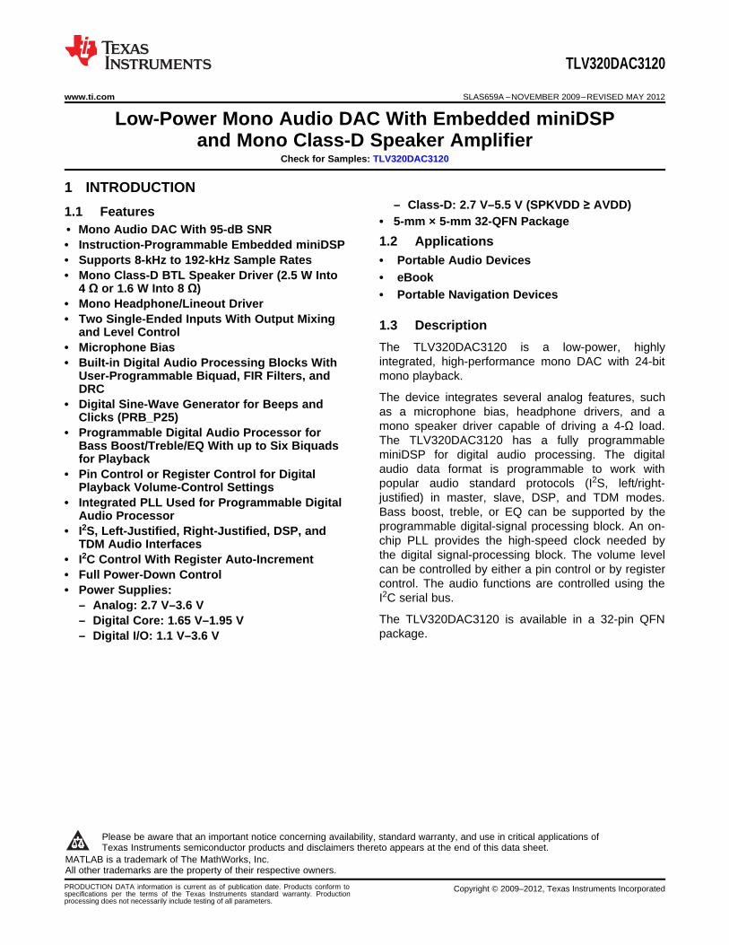
Digital
Audio
Processing
and
Serial
Interface
SDIN
BCLK
WCLK
MCLK PLL
HPVDDHPVSS SPKVDDSPKVSSAVDDAVSS SPKVSS SPKVDD
VOL/MICDET
SCL
SDA
GPIOGPIO1
DAC
MIXER
P1/R35
RESET
DVDDDVSSIOVDDIOVSS
AIN2
AIN1
2 V/2.5 V/AVDDMICBIAS
Note: Normally,MCLK is PLL input;however, BCLK orGPIO1 can also bePLL input.
Audio Output Stage
Power Management
De-Pop
and
Soft Start
RC CLK
P1/R33–R34
P1/R46
I C2
Mono DAC
SPKP
SPKM
Class-D SpeakerDriver
6 dB to 24 dB(6-dB steps)
AnalogAttenuation
0 dB to –78 dBand Mute
(0.5-dB steps)
P1/R42P1/R38SPKP
SPKM
Class A/BHeadphone/Lineout
Driver
0 dB to 9 dB(1-dB steps)
AnalogAttenuation
HPOUT
P1/R36 P1/R40
P1/R30–R31
L Data
R Data
(L+R)/2 Data
P0/R63
7-Bit ADC P0/R116
Left and RightVolume-Control Register
P0/R117
Digital Vol24 dB to
MuteminiDSP
P0/R64
S
0 dB to –78 dBand Mute
(0.5-dB steps)
B0360-01
TLV320DAC3120
SLAS659A –NOVEMBER 2009–REVISED MAY 2012 www.ti.com
This integrated circuit can be damaged by ESD. Texas Instruments recommends that all integrated circuits be handled withappropriate precautions. Failure to observe proper handling and installation procedures can cause damage.
ESD damage can range from subtle performance degradation to complete device failure. Precision integrated circuits may be moresusceptible to damage because very small parametric changes could cause the device not to meet its published specifications.
Figure 1-1. Functional Block Diagram
NOTEThis data manual is designed using PDF document-viewing features that allow quick accessto information. For example, performing a global search on "page 0 / register 27" producesall references to this page and register in a list. This makes is easy to traverse the list andfind all information related to a page and register. Note that the search string must be of theindicated format. Also, this document includes document hyperlinks to allow the user toquickly find a document reference. To come back to the original page, click the green leftarrow near the PDF page number at the bottom of the file. The hot-key for this function is alt-left arrow on the keyboard. Another way to find information quickly is to use the PDFbookmarks.
2 INTRODUCTION Copyright © 2009–2012, Texas Instruments Incorporated
Submit Documentation FeedbackProduct Folder Link(s): TLV320DAC3120
P0048-12
AVSSSPKVSS
IOV
SS
SP
KV
DD
24
1
23
2
22
3
21
4
20
5
19
6
18
7
17
8
1625
1526
1427
1328
1229
1130
1031
932
NC
SP
KM
AIN2
SP
KP
AIN1
SP
KV
DD
MICBIAS
SP
KV
SS
VOL/MICDET
SP
KM
SCL
DV
SS
SDA
AV
DD
RHB Package(Top View)
SPKP
IOV
DD
HPOUT
DV
DD
HPVDD
NC
HPVSS
DIN
NC
WC
LK
RESET
BC
LK
GPIO1
MC
LK
TLV320DAC3120
TLV320DAC3120
www.ti.com SLAS659A –NOVEMBER 2009–REVISED MAY 2012
2 PACKAGE AND SIGNAL DESCRIPTIONS
2.1 Package/Ordering InformationOPERATING TRANSPORT MEDIA,PACKAGEPRODUCT PACKAGE TEMPERATURE ORDERING NUMBER QUANTITYDESIGNATOR RANGE
TLV320DAC3120IRHBT Tape and reel, 250TLV320DAC3120 QFN-32 RHB –40°C to 85°C
TLV320DAC3120IRHBR Tape and reel, 3000
2.2 Device Information
Table 2-1. TERMINAL FUNCTIONS
TERMINALI/O DESCRIPTION
NAME NO.
AIN1 13 I Analog input #1 routed to output mixer
AIN2 14 I Analog input #2 routed to output mixer
AVDD 17 – Analog power supply
AVSS 16 – Analog ground
BCLK 7 I/O Audio serial bit clock
DIN 5 I Audio serial data input
DVDD 3 – Digital power – digital core
DVSS 18 – Digital ground
GPIO1 32 I/O General-purpose input/output and multifunction pin
HPOUT 27 O Headphone/lineout driver output
HPVDD 28 – Headphone/line driver and PLL power
HPVSS 29 – Headphone/line driver and PLL ground
IOVDD 2 – Interface power
IOVSS 1 – Interface ground
MCLK 8 I Exterrnal master clock
MICBIAS 12 O Micophone bias voltage
Copyright © 2009–2012, Texas Instruments Incorporated PACKAGE AND SIGNAL DESCRIPTIONS 3Submit Documentation Feedback
Product Folder Link(s): TLV320DAC3120
TLV320DAC3120
SLAS659A –NOVEMBER 2009–REVISED MAY 2012 www.ti.com
Table 2-1. TERMINAL FUNCTIONS (continued)
TERMINALI/O DESCRIPTION
NAME NO.
NC 4, 15, 30 – No connection
RESET 31 I Device reset
SCL 10 I/O I2C control-bus clock input
SDA 9 I/O I2C control-bus data input
SPKM 19, 23 O Class-D speaker driver inverting output
SPKP 22, 26 O Class-D speaker driver noninverting output
SPKVDD 21, 24 – Class-D speaker driver power supply
SPKVSS 20, 25 – Class-D speaker driver power-supply ground
VOL/MICDET 11 I Volume control or microphone/headphone/headset detection
WCLK 6 I/O Audio serial word clock
3 ELECTRICAL SPECIFICATIONS
3.1 Absolute Maximum Ratingsover operating free-air temperature range (unless otherwise noted) (1)
VALUE UNIT
AVDD to AVSS –0.3 to 3.9 V
DVDD to DVSS –0.3 to 2.5 V
HPVDD to HPVSS –0.3 to 3.9 V
SPKVDD to SPKVSS –0.3 to 6 V
IOVDD to IOVSS –0.3 to 3.9 V
Digital input voltage IOVSS – 0.3 to IOVDD + 0.3 V
Analog input voltage AVSS – 0.3 to AVDD + 0.3 V
Operating temperature range –40 to 85 °C
Storage temperature range –55 to 150 °C
Junction temperature (TJ Max) 105 °C
Power dissipation (TJ Max – TA)/RθJA WQFN package
RθJA Thermal impedance (with thermal pad soldered to board) 35 °C/W
(1) Stresses beyond those listed under Absolute Maximum Ratings may cause permanent damage to the device. These are stress ratingsonly, and functional operation of the device at these or any other conditions beyond those indicated under Recommended OperatingConditions is not implied. Exposure to absolute-maximum-rated conditions for extended periods may affect device reliability.
Table 3-1. System Thermal Characteristics (1)
Power Rating at 25°C Derating Factor Power Rating at 70°C Power Rating at 85°C
2.3 W 28.57 mW/°C 1 W 0.6 W
(1) This data was taken using 2-oz. (0.071-mm thick) trace and copper pad that is soldered to a JEDEC high-K, standard 4-layer 3-in. × 3-in. (7.62-cm × 7.62-cm) PCB.
4 ELECTRICAL SPECIFICATIONS Copyright © 2009–2012, Texas Instruments Incorporated
Submit Documentation FeedbackProduct Folder Link(s): TLV320DAC3120
TLV320DAC3120
www.ti.com SLAS659A –NOVEMBER 2009–REVISED MAY 2012
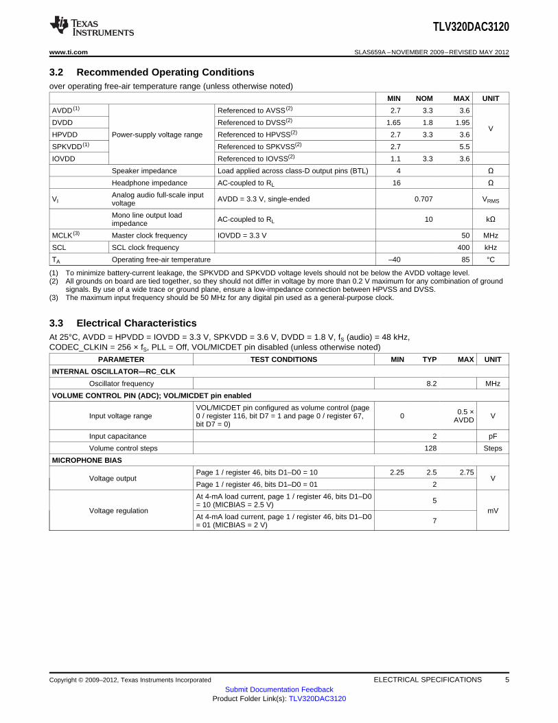
3.2 Recommended Operating Conditionsover operating free-air temperature range (unless otherwise noted)
MIN NOM MAX UNIT
AVDD (1) Referenced to AVSS (2) 2.7 3.3 3.6
DVDD Referenced to DVSS(2) 1.65 1.8 1.95V
HPVDD Power-supply voltage range Referenced to HPVSS(2) 2.7 3.3 3.6
SPKVDD (1) Referenced to SPKVSS(2) 2.7 5.5
IOVDD Referenced to IOVSS(2) 1.1 3.3 3.6
Speaker impedance Load applied across class-D output pins (BTL) 4 ΩHeadphone impedance AC-coupled to RL 16 ΩAnalog audio full-scale inputVI AVDD = 3.3 V, single-ended 0.707 VRMSvoltage
Mono line output load AC-coupled to RL 10 kΩimpedance
MCLK (3) Master clock frequency IOVDD = 3.3 V 50 MHz
SCL SCL clock frequency 400 kHz
TA Operating free-air temperature –40 85 °C
(1) To minimize battery-current leakage, the SPKVDD and SPKVDD voltage levels should not be below the AVDD voltage level.(2) All grounds on board are tied together, so they should not differ in voltage by more than 0.2 V maximum for any combination of ground
signals. By use of a wide trace or ground plane, ensure a low-impedance connection between HPVSS and DVSS.(3) The maximum input frequency should be 50 MHz for any digital pin used as a general-purpose clock.
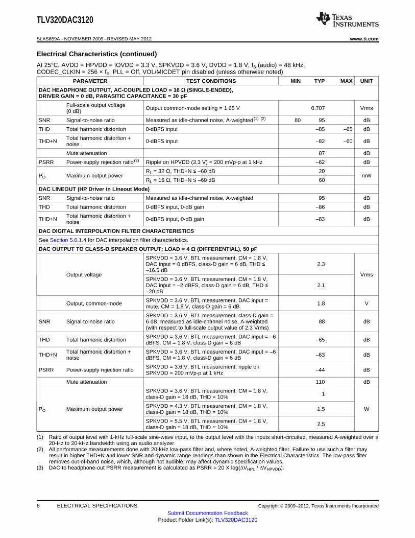
3.3 Electrical CharacteristicsAt 25°C, AVDD = HPVDD = IOVDD = 3.3 V, SPKVDD = 3.6 V, DVDD = 1.8 V, fS (audio) = 48 kHz,CODEC_CLKIN = 256 × fS, PLL = Off, VOL/MICDET pin disabled (unless otherwise noted)
PARAMETER TEST CONDITIONS MIN TYP MAX UNIT
INTERNAL OSCILLATOR—RC_CLK
Oscillator frequency 8.2 MHz
VOLUME CONTROL PIN (ADC); VOL/MICDET pin enabled
VOL/MICDET pin configured as volume control (page 0.5 ×Input voltage range 0 / register 116, bit D7 = 1 and page 0 / register 67, 0 VAVDDbit D7 = 0)
Input capacitance 2 pF
Volume control steps 128 Steps
MICROPHONE BIAS
Page 1 / register 46, bits D1–D0 = 10 2.25 2.5 2.75Voltage output V
Page 1 / register 46, bits D1–D0 = 01 2
At 4-mA load current, page 1 / register 46, bits D1–D0 5= 10 (MICBIAS = 2.5 V)Voltage regulation mV
At 4-mA load current, page 1 / register 46, bits D1–D0 7= 01 (MICBIAS = 2 V)
Copyright © 2009–2012, Texas Instruments Incorporated ELECTRICAL SPECIFICATIONS 5Submit Documentation Feedback
Product Folder Link(s): TLV320DAC3120
TLV320DAC3120
SLAS659A –NOVEMBER 2009–REVISED MAY 2012 www.ti.com
Electrical Characteristics (continued)
At 25°C, AVDD = HPVDD = IOVDD = 3.3 V, SPKVDD = 3.6 V, DVDD = 1.8 V, fS (audio) = 48 kHz,CODEC_CLKIN = 256 × fS, PLL = Off, VOL/MICDET pin disabled (unless otherwise noted)
PARAMETER TEST CONDITIONS MIN TYP MAX UNIT
DAC HEADPHONE OUTPUT, AC-COUPLED LOAD = 16 Ω (SINGLE-ENDED),DRIVER GAIN = 0 dB, PARASITIC CAPACITANCE = 30 pF
Full-scale output voltage Output common-mode setting = 1.65 V 0.707 Vrms(0 dB)
SNR Signal-to-noise ratio Measured as idle-channel noise, A-weighted (1) (2) 80 95 dB
THD Total harmonic distortion 0-dBFS input –85 –65 dB
Total harmonic distortion +THD+N 0-dBFS input –82 –60 dBnoise
Mute attenuation 87 dB
PSRR Power-supply rejection ratio (3) Ripple on HPVDD (3.3 V) = 200 mVp-p at 1 kHz –62 dB
RL = 32 Ω, THD+N ≤ –60 dB 20PO Maximum output power mW
RL = 16 Ω, THD+N ≤ –60 dB 60
DAC LINEOUT (HP Driver in Lineout Mode)
SNR Signal-to-noise ratio Measured as idle-channel noise, A-weighted 95 dB
THD Total harmonic distortion 0-dBFS input, 0-dB gain –86 dB
Total harmonic distortion +THD+N 0-dBFS input, 0-dB gain –83 dBnoise
DAC DIGITAL INTERPOLATION FILTER CHARACTERISTICS
See Section 5.6.1.4 for DAC interpolation filter characteristics.
DAC OUTPUT TO CLASS-D SPEAKER OUTPUT; LOAD = 4 Ω (DIFFERENTIAL), 50 pF
SPKVDD = 3.6 V, BTL measurement, CM = 1.8 V,DAC input = 0 dBFS, class-D gain = 6 dB, THD ≤ 2.3–16.5 dB
Output voltage VrmsSPKVDD = 3.6 V, BTL measurement, CM = 1.8 V,DAC input = –2 dBFS, class-D gain = 6 dB, THD ≤ 2.1–20 dB
SPKVDD = 3.6 V, BTL measurement, DAC input =Output, common-mode 1.8 Vmute, CM = 1.8 V, class-D gain = 6 dB
SPKVDD = 3.6 V, BTL measurement, class-D gain =SNR Signal-to-noise ratio 6 dB, measured as idle-channel noise, A-weighted 88 dB
(with respect to full-scale output value of 2.3 Vrms)
SPKVDD = 3.6 V, BTL measurement, DAC input = –6THD Total harmonic distortion –65 dBdBFS, CM = 1.8 V, class-D gain = 6 dB
Total harmonic distortion + SPKVDD = 3.6 V, BTL measurement, DAC input = –6THD+N –63 dBnoise dBFS, CM = 1.8 V, class-D gain = 6 dB
SPKVDD = 3.6 V, BTL measurement, ripple onPSRR Power-supply rejection ratio –44 dBSPKVDD = 200 mVp-p at 1 kHz
Mute attenuation 110 dB
SPKVDD = 3.6 V, BTL measurement, CM = 1.8 V, 1class-D gain = 18 dB, THD = 10%
SPKVDD = 4.3 V, BTL measurement, CM = 1.8 V,PO Maximum output power 1.5 Wclass-D gain = 18 dB, THD = 10%
SPKVDD = 5.5 V, BTL measurement, CM = 1.8 V, 2.5class-D gain = 18 dB, THD = 10%
(1) Ratio of output level with 1-kHz full-scale sine-wave input, to the output level with the inputs short-circuited, measured A-weighted over a20-Hz to 20-kHz bandwidth using an audio analyzer.
(2) All performance measurements done with 20-kHz low-pass filter and, where noted, A-weighted filter. Failure to use such a filter mayresult in higher THD+N and lower SNR and dynamic range readings than shown in the Electrical Characteristics. The low-pass filterremoves out-of-band noise, which, although not audible, may affect dynamic specification values.
(3) DAC to headphone-out PSRR measurement is calculated as PSRR = 20 X log(∆VHPL / ∆VHPVDD).
6 ELECTRICAL SPECIFICATIONS Copyright © 2009–2012, Texas Instruments Incorporated
Submit Documentation FeedbackProduct Folder Link(s): TLV320DAC3120
TLV320DAC3120
www.ti.com SLAS659A –NOVEMBER 2009–REVISED MAY 2012
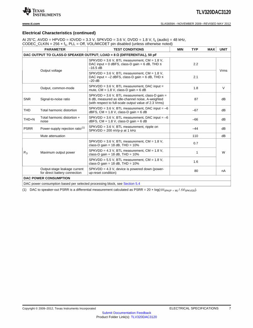
Electrical Characteristics (continued)
At 25°C, AVDD = HPVDD = IOVDD = 3.3 V, SPKVDD = 3.6 V, DVDD = 1.8 V, fS (audio) = 48 kHz,CODEC_CLKIN = 256 × fS, PLL = Off, VOL/MICDET pin disabled (unless otherwise noted)
PARAMETER TEST CONDITIONS MIN TYP MAX UNIT
DAC OUTPUT TO CLASS-D SPEAKER OUTPUT; LOAD = 8 Ω (DIFFERENTIAL), 50 pF
SPKVDD = 3.6 V, BTL measurement, CM = 1.8 V,DAC input = 0 dBFS, class-D gain = 6 dB, THD ≤ 2.2–16.5 dB
Output voltage VrmsSPKVDD = 3.6 V, BTL measurement, CM = 1.8 V,DAC input = –2 dBFS, class-D gain = 6 dB, THD ≤ 2.1–20 dB
SPKVDD = 3.6 V, BTL measurement, DAC input =Output, common-mode 1.8 Vmute, CM = 1.8 V, class-D gain = 6 dB
SPKVDD = 3.6 V, BTL measurement, class-D gain =SNR Signal-to-noise ratio 6 dB, measured as idle-channel noise, A-weighted 87 dB
(with respect to full-scale output value of 2.3 Vrms)
SPKVDD = 3.6 V, BTL measurement, DAC input = –6THD Total harmonic distortion –67 dBdBFS, CM = 1.8 V, class-D gain = 6 dB
Total harmonic distortion + SPKVDD = 3.6 V, BTL measurement, DAC input = –6THD+N –66 dBnoise dBFS, CM = 1.8 V, class-D gain = 6 dB
SPKVDD = 3.6 V, BTL measurement, ripple onPSRR Power-supply rejection ratio (1) –44 dBSPKVDD = 200 mVp-p at 1 kHz
Mute attenuation 110 dB
SPKVDD = 3.6 V, BTL measurement, CM = 1.8 V, 0.7class-D gain = 18 dB, THD = 10%
SPKVDD = 4.3 V, BTL measurement, CM = 1.8 V,PO Maximum output power 1 Wclass-D gain = 18 dB, THD = 10%
SPKVDD = 5.5 V, BTL measurement, CM = 1.8 V, 1.6class-D gain = 18 dB, THD = 10%
Output-stage leakage current SPKVDD = 4.3 V, device is powered down (power- 80 nAfor direct battery connection up-reset condition)
DAC POWER CONSUMPTION
DAC power consumption based per selected processing block, see Section 5.4
(1) DAC to speaker-out PSRR is a differential measurement calculated as PSRR = 20 × log(∆VSPK(P + M) / ∆VSPKVDD).
Copyright © 2009–2012, Texas Instruments Incorporated ELECTRICAL SPECIFICATIONS 7Submit Documentation Feedback
Product Folder Link(s): TLV320DAC3120
T0145-10
WCLK
BCLK
DIN
t (WS)d
t (DI)S t (DI)h
tr
tf
TLV320DAC3120
SLAS659A –NOVEMBER 2009–REVISED MAY 2012 www.ti.com
Electrical Characteristics (continued)
At 25°C, AVDD = HPVDD = IOVDD = 3.3 V, SPKVDD = 3.6 V, DVDD = 1.8 V, fS (audio) = 48 kHz,CODEC_CLKIN = 256 × fS, PLL = Off, VOL/MICDET pin disabled (unless otherwise noted)
PARAMETER TEST CONDITIONS MIN TYP MAX UNIT
DIGITAL INPUT/OUTPUT
Logic family CMOS
0.7 ×IIH = 5 μA, IOVDD ≥ 1.6 V IOVDDVIH VIIH = 5 μA, IOVDD < 1.6 V IOVDD
0.3 ×IIL = 5 μA, IOVDD ≥ 1.6 V –0.3 IOVDDVIL VLogic levelIIL = 5 μA, IOVDD < 1.6 V 0
0.8 ×VOH IOH = 2 TTL loads VIOVDD
0.1 ×VOL IOL = 2 TTL loads VIOVDD
Capacitive load 10 pF
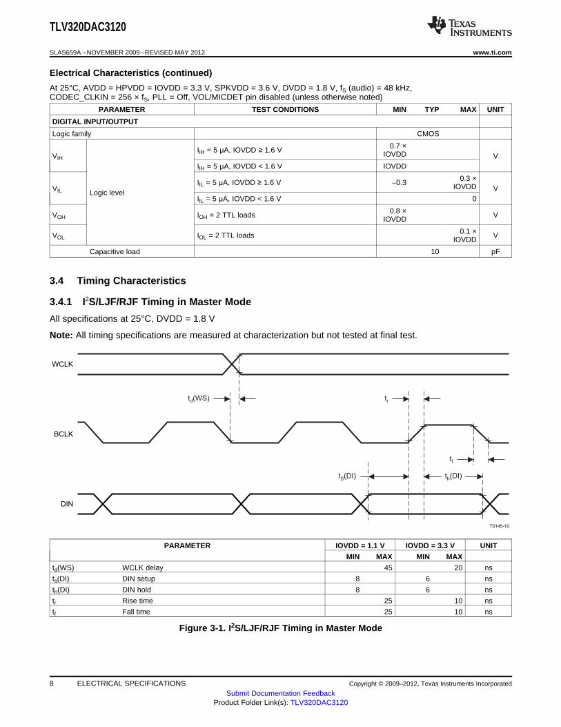
3.4 Timing Characteristics
3.4.1 I2S/LJF/RJF Timing in Master Mode
All specifications at 25°C, DVDD = 1.8 V
Note: All timing specifications are measured at characterization but not tested at final test.
PARAMETER IOVDD = 1.1 V IOVDD = 3.3 V UNIT
MIN MAX MIN MAX
td(WS) WCLK delay 45 20 ns
ts(DI) DIN setup 8 6 ns
th(DI) DIN hold 8 6 ns
tr Rise time 25 10 ns
tf Fall time 25 10 ns
Figure 3-1. I2S/LJF/RJF Timing in Master Mode
8 ELECTRICAL SPECIFICATIONS Copyright © 2009–2012, Texas Instruments Incorporated
Submit Documentation FeedbackProduct Folder Link(s): TLV320DAC3120
T0145-11
WCLK
BCLK
DIN
t (WS)h
t (BCLK)H
t (DI)S
t (BCLK)L
t (DI)h
t (WS)S
tr
tf
TLV320DAC3120
www.ti.com SLAS659A –NOVEMBER 2009–REVISED MAY 2012
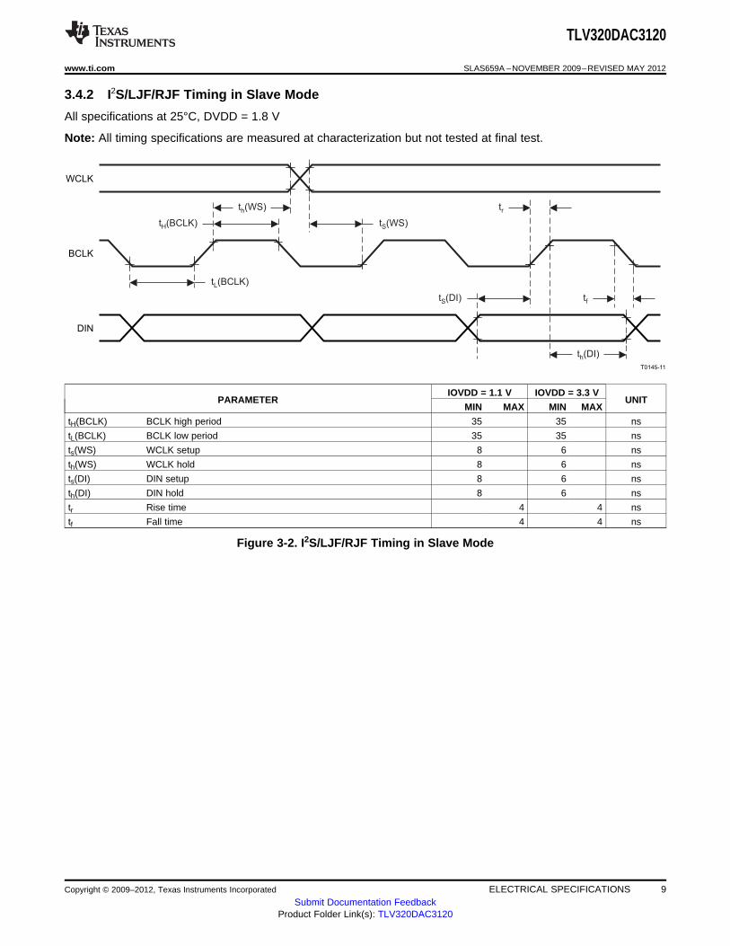
3.4.2 I2S/LJF/RJF Timing in Slave Mode
All specifications at 25°C, DVDD = 1.8 V
Note: All timing specifications are measured at characterization but not tested at final test.
IOVDD = 1.1 V IOVDD = 3.3 VPARAMETER UNIT
MIN MAX MIN MAX
tH(BCLK) BCLK high period 35 35 ns
tL(BCLK) BCLK low period 35 35 ns
ts(WS) WCLK setup 8 6 ns
th(WS) WCLK hold 8 6 ns
ts(DI) DIN setup 8 6 ns
th(DI) DIN hold 8 6 ns
tr Rise time 4 4 ns
tf Fall time 4 4 ns
Figure 3-2. I2S/LJF/RJF Timing in Slave Mode
Copyright © 2009–2012, Texas Instruments Incorporated ELECTRICAL SPECIFICATIONS 9Submit Documentation Feedback
Product Folder Link(s): TLV320DAC3120
T0146-09
WCLK
BCLK
DIN
t (WS)d t (WS)d
t (DI)S
t (DI)h
tf
tr
TLV320DAC3120
SLAS659A –NOVEMBER 2009–REVISED MAY 2012 www.ti.com
3.4.3 DSP Timing in Master Mode
All specifications at 25°C, DVDD = 1.8 V
Note: All timing specifications are measured at characterization but not tested at final test.
IOVDD = 1.1 V IOVDD = 3.3 VPARAMETER UNIT
MIN MAX MIN MAX
td(WS) WCLK delay 45 20 ns
ts(DI) DIN setup 8 8 ns
th(DI) DIN hold 8 8 ns
tr Rise time 25 10 ns
tf Fall time 25 10 ns
Figure 3-3. DSP Timing in Master Mode
10 ELECTRICAL SPECIFICATIONS Copyright © 2009–2012, Texas Instruments Incorporated
Submit Documentation FeedbackProduct Folder Link(s): TLV320DAC3120
T0146-10
WCLK
BCLK
DIN
t (WS)h t (WS)h
t (BCLK)L
tr
tf
t (DI)St (BCLK)H
t (DI)h
t (WS)S t (WS)S
TLV320DAC3120
www.ti.com SLAS659A –NOVEMBER 2009–REVISED MAY 2012
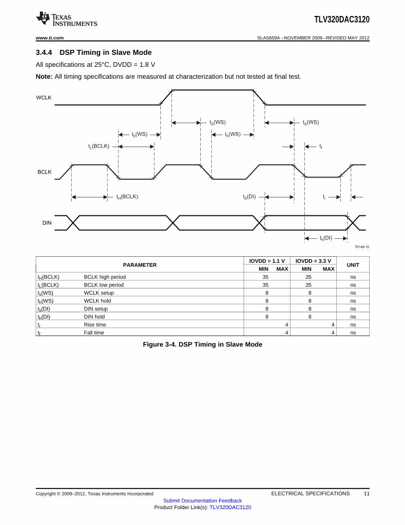
3.4.4 DSP Timing in Slave Mode
All specifications at 25°C, DVDD = 1.8 V
Note: All timing specifications are measured at characterization but not tested at final test.
IOVDD = 1.1 V IOVDD = 3.3 VPARAMETER UNIT
MIN MAX MIN MAX
tH(BCLK) BCLK high period 35 35 ns
tL(BCLK) BCLK low period 35 35 ns
ts(WS) WCLK setup 8 8 ns
th(WS) WCLK hold 8 8 ns
ts(DI) DIN setup 8 8 ns
th(DI) DIN hold 8 8 ns
tr Rise time 4 4 ns
tf Fall time 4 4 ns
Figure 3-4. DSP Timing in Slave Mode
Copyright © 2009–2012, Texas Instruments Incorporated ELECTRICAL SPECIFICATIONS 11Submit Documentation Feedback
Product Folder Link(s): TLV320DAC3120
STO STA STA STO
SDA
SCL
tBUF tLOW
tSU;STA
tHIGH tHD;STA
tr
tHD;STA
tHD;DAT
tSU;DAT tSU;STO
tf
T0295-02
TLV320DAC3120
SLAS659A –NOVEMBER 2009–REVISED MAY 2012 www.ti.com
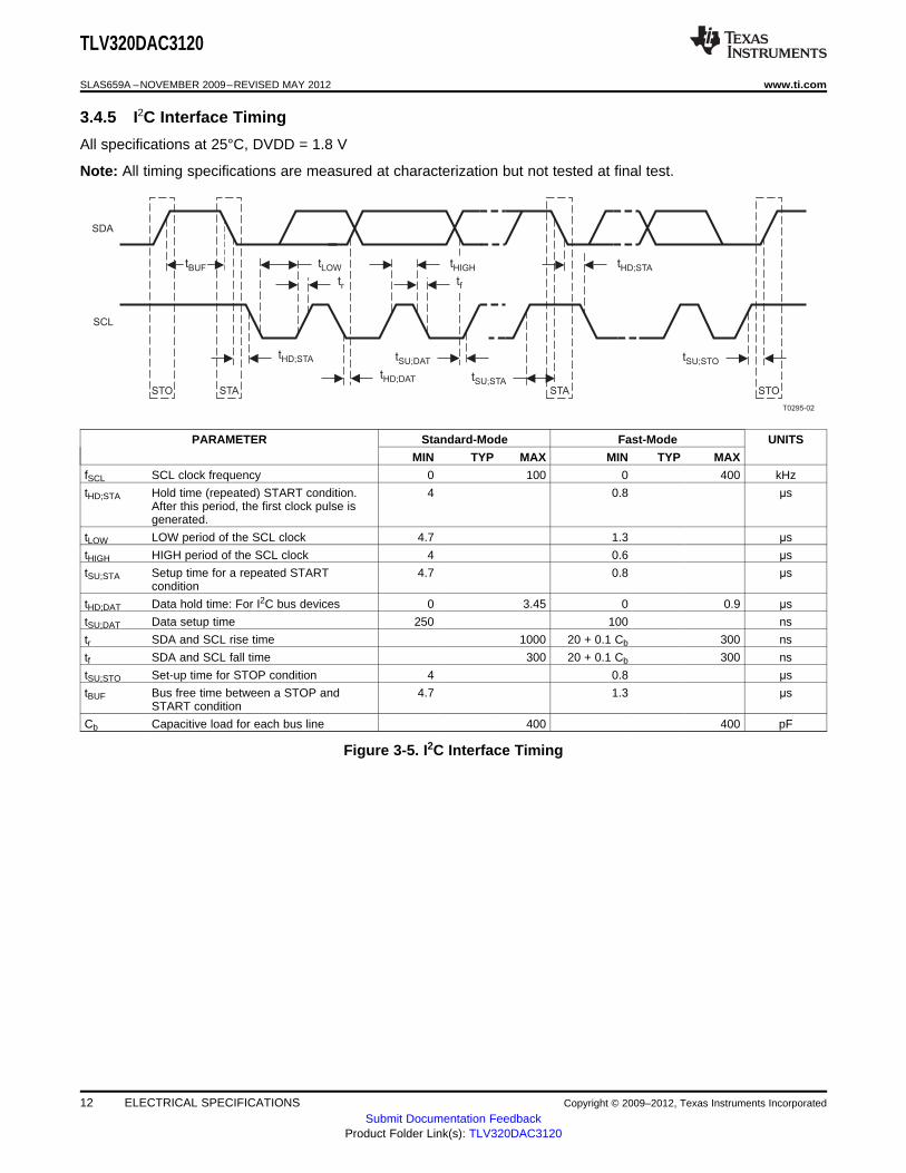
3.4.5 I2C Interface Timing
All specifications at 25°C, DVDD = 1.8 V
Note: All timing specifications are measured at characterization but not tested at final test.
PARAMETER Standard-Mode Fast-Mode UNITS
MIN TYP MAX MIN TYP MAX
fSCL SCL clock frequency 0 100 0 400 kHz
tHD;STA Hold time (repeated) START condition. 4 0.8 μsAfter this period, the first clock pulse isgenerated.
tLOW LOW period of the SCL clock 4.7 1.3 μs
tHIGH HIGH period of the SCL clock 4 0.6 μs
tSU;STA Setup time for a repeated START 4.7 0.8 μscondition
tHD;DAT Data hold time: For I2C bus devices 0 3.45 0 0.9 μs
tSU;DAT Data setup time 250 100 ns
tr SDA and SCL rise time 1000 20 + 0.1 Cb 300 ns
tf SDA and SCL fall time 300 20 + 0.1 Cb 300 ns
tSU;STO Set-up time for STOP condition 4 0.8 μs
tBUF Bus free time between a STOP and 4.7 1.3 μsSTART condition
Cb Capacitive load for each bus line 400 400 pF
Figure 3-5. I2C Interface Timing
12 ELECTRICAL SPECIFICATIONS Copyright © 2009–2012, Texas Instruments Incorporated
Submit Documentation FeedbackProduct Folder Link(s): TLV320DAC3120
−100
−90
−80
−70
−60
−50
−40
−30
−20
−10
0
0.00 0.02 0.04 0.06 0.08 0.10 0.12 0.14
G003
TH
D+N
− T
otal
Har
mon
ic D
isto
rtio
n +
Noi
se −
dB
PO − Output Power − W
HPVDD = 3.3 VCM = 1.65 V
HPVDD = 3.6 VCM = 1.8 V
HPVDD = 3 VCM = 1.5 V
HPVDD = 2.7 VCM = 1.35 V
IOVDD = 3.3 VDVDD = 1.8 VDriver Gain = 9 dBRL = 16 Ω
f − Frequency − kHz
−160
−140
−120
−100
−80
−60
−40
−20
0
0 5 10 15 20
Am
plitu
de −
dB
FS
G001
AVDD = HPVDD = 3.3 VIOVDD = SPKVDD = 3.3 VDVDD = 1.8 V
f − Frequency − kHz
−160
−140
−120
−100
−80
−60
−40
−20
0
0 5 10 15 20
Am
plitu
de −
dB
FS
G002
AVDD = HPVDD = 3.3 VIOVDD = SPKVDD = 3.3 VDVDD = 1.8 V
TLV320DAC3120
www.ti.com SLAS659A –NOVEMBER 2009–REVISED MAY 2012
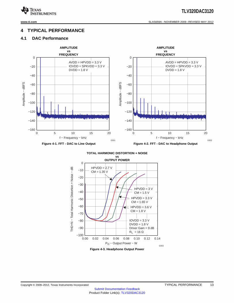
4 TYPICAL PERFORMANCE
4.1 DAC PerformanceTEXT ADDED FOR SPACING
AMPLITUDE AMPLITUDEvs vs
FREQUENCY FREQUENCY
Figure 4-1. FFT - DAC to Line Output Figure 4-2. FFT - DAC to Headphone OutputTEXT ADDED FOR SPACING TEXT ADDED FOR SPACING
TOTAL HARMONIC DISTORTION + NOISEvs
OUTPUT POWER
Figure 4-3. Headphone Output Power
Copyright © 2009–2012, Texas Instruments Incorporated TYPICAL PERFORMANCE 13Submit Documentation Feedback
Product Folder Link(s): TLV320DAC3120
−70
−60
−50
−40
−30
−20
−10
0
0.0 0.5 1.0 1.5 2.0 2.5
G006
TH
D+N
− T
otal
Har
mon
ic D
isto
rtio
n +
Noi
se −
dB
PO − Output Power − W
Driver Gain= 6 dB
Driver Gain= 12 dB
AVDD = HPVDD = 3.3 VIOVDD = 3.3 VSPKVDD = 5.5 VDVDD = 1.8 VRL = 8 Ω
Driver Gain= 24 dB
Driver Gain= 18 dB
−70
−60
−50
−40
−30
−20
−10
0
0.0 0.5 1.0 1.5 2.0 2.5 3.0
G007
TH
D+N
− T
otal
Har
mon
ic D
isto
rtio
n +
Noi
se −
dB
PO − Output Power − W
AVDD = 3.3 VHPVDD = 3.3 VIOVDD = 3.3 VDVDD = 1.8 VDriver Gain = 18 dBRL = 8 Ω
SPKVDD = 5.5 V
SPKVDD = 4.3 V
SPKVDD = 3.3 V
SPKVDD = 3.6 V
−70
−60
−50
−40
−30
−20
−10
0
0.0 0.5 1.0 1.5 2.0 2.5 3.0 3.5 4.0
G004
TH
D+N
− T
otal
Har
mon
ic D
isto
rtio
n +
Noi
se −
dB
PO − Output Power − W
Driver Gain= 6 dB
Driver Gain= 12 dB
AVDD = HPVDD = 3.3 VIOVDD = 3.3 VSPKVDD = 5.5 VDVDD = 1.8 VRL = 4 Ω
Driver Gain= 18 dB
Driver Gain= 24 dB
−70
−60
−50
−40
−30
−20
−10
0
0.0 0.5 1.0 1.5 2.0 2.5 3.0 3.5 4.0
G005
TH
D+N
− T
otal
Har
mon
ic D
isto
rtio
n +
Noi
se −
dB
PO − Output Power − W
AVDD = 3.3 VHPVDD = 3.3 VIOVDD = 3.3 VDVDD = 1.8 VDriver Gain = 18 dBRL = 4 Ω
SPKVDD = 5.5 V
SPKVDD = 4.3 V
SPKVDD = 3.3 V
SPKVDD = 3.6 V
TLV320DAC3120
SLAS659A –NOVEMBER 2009–REVISED MAY 2012 www.ti.com
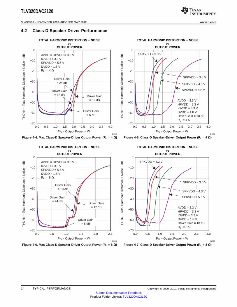
4.2 Class-D Speaker Driver PerformanceTEXT ADDED FOR SPACING
TOTAL HARMONIC DISTORTION + NOISE TOTAL HARMONIC DISTORTION + NOISEvs vs
OUTPUT POWER OUTPUT POWER
Figure 4-4. Max Class-D Speaker-Driver Output Power (RL = 4 Ω) Figure 4-5. Class-D Speaker-Driver Output Power (RL = 4 Ω)TEXT ADDED FOR SPACING TEXT ADDED FOR SPACING
TOTAL HARMONIC DISTORTION + NOISE TOTAL HARMONIC DISTORTION + NOISEvs vs
OUTPUT POWER OUTPUT POWER
Figure 4-6. Max Class-D Speaker-Driver Output Power (RL = 8 Ω) Figure 4-7. Class-D Speaker-Driver Output Power (RL = 8 Ω)
14 TYPICAL PERFORMANCE Copyright © 2009–2012, Texas Instruments Incorporated
Submit Documentation FeedbackProduct Folder Link(s): TLV320DAC3120
f − Frequency − kHz
−160
−140
−120
−100
−80
−60
−40
−20
0
0 5 10 15 20
Am
plitu
de −
dB
FS
G008
AVDD = HPVDD = 3.3 VIOVDD = SPKVDD = 3.3 VDVDD = 1.8 V
f − Frequency − kHz
−160
−140
−120
−100
−80
−60
−40
−20
0
0 5 10 15 20
Am
plitu
de −
dB
FS
G009
AVDD = HPVDD = 3.3 VIOVDD = SPKVDD = 3.3 VDVDD = 1.8 V
TLV320DAC3120
www.ti.com SLAS659A –NOVEMBER 2009–REVISED MAY 2012
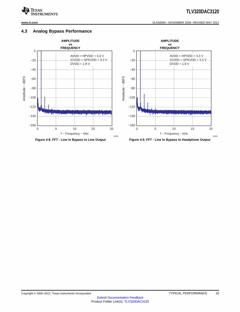
4.3 Analog Bypass PerformanceTEXT ADDED FOR SPACING
AMPLITUDE AMPLITUDEvs vs
FREQUENCY FREQUENCY
Figure 4-8. FFT - Line In Bypass to Line Output Figure 4-9. FFT - Line In Bypass to Headphone Output
Copyright © 2009–2012, Texas Instruments Incorporated TYPICAL PERFORMANCE 15Submit Documentation Feedback
Product Folder Link(s): TLV320DAC3120
I − Current − mA
0.0
0.5
1.0
1.5
2.0
2.5
3.0
3.5
0.0 0.5 1.0 1.5 2.0 2.5 3.0 3.5 4.0
V −
Vol
tage
− V
G010
Micbias = 2 V
Micbias = 2.5 V
Micbias = AVDD (3.3 V)
TLV320DAC3120
SLAS659A –NOVEMBER 2009–REVISED MAY 2012 www.ti.com
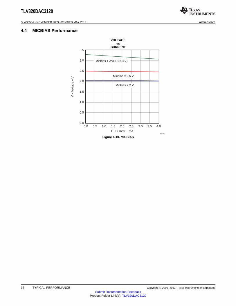
4.4 MICBIAS PerformanceTEXT ADDED FOR SPACING
VOLTAGEvs
CURRENT
Figure 4-10. MICBIAS
16 TYPICAL PERFORMANCE Copyright © 2009–2012, Texas Instruments Incorporated
Submit Documentation FeedbackProduct Folder Link(s): TLV320DAC3120
HPVDD HPVSSSPKVDD SPKVSS AVDD AVSSSPKVSS
VOL/MICDET
MICBIAS
TLV320DAC3120
SPKVDD
22 Fm0.1 Fm0.1 Fm 22 Fm
SVDD
AVDD
AVSS
0.1 Fm 10 Fm0.1 Fm 10 Fm
+3.3VA
1 Fm
DVDD DVSS IOVDD IOVSS
0.1 Fm 10 Fm
+1.8VD IOVDD
0.1 Fm 10 Fm
Host P
rocessor
SDIN
BCLK
WCLK
MCLK
SCL
SDA
RESET
GPIO1
S0400-06
AIN1
AIN2
To ExternalMIC Circuitry
Analog In
SPKM
SPKM
SPKP
SPKP
HPR
HPL
8- orSpeaker
W 4-W
StereoHeadphoneOut
R1
34.8 kW
P1
25 kW
R2
9.76 kW
TLV320DAC3120
www.ti.com SLAS659A –NOVEMBER 2009–REVISED MAY 2012
5 APPLICATION INFORMATION
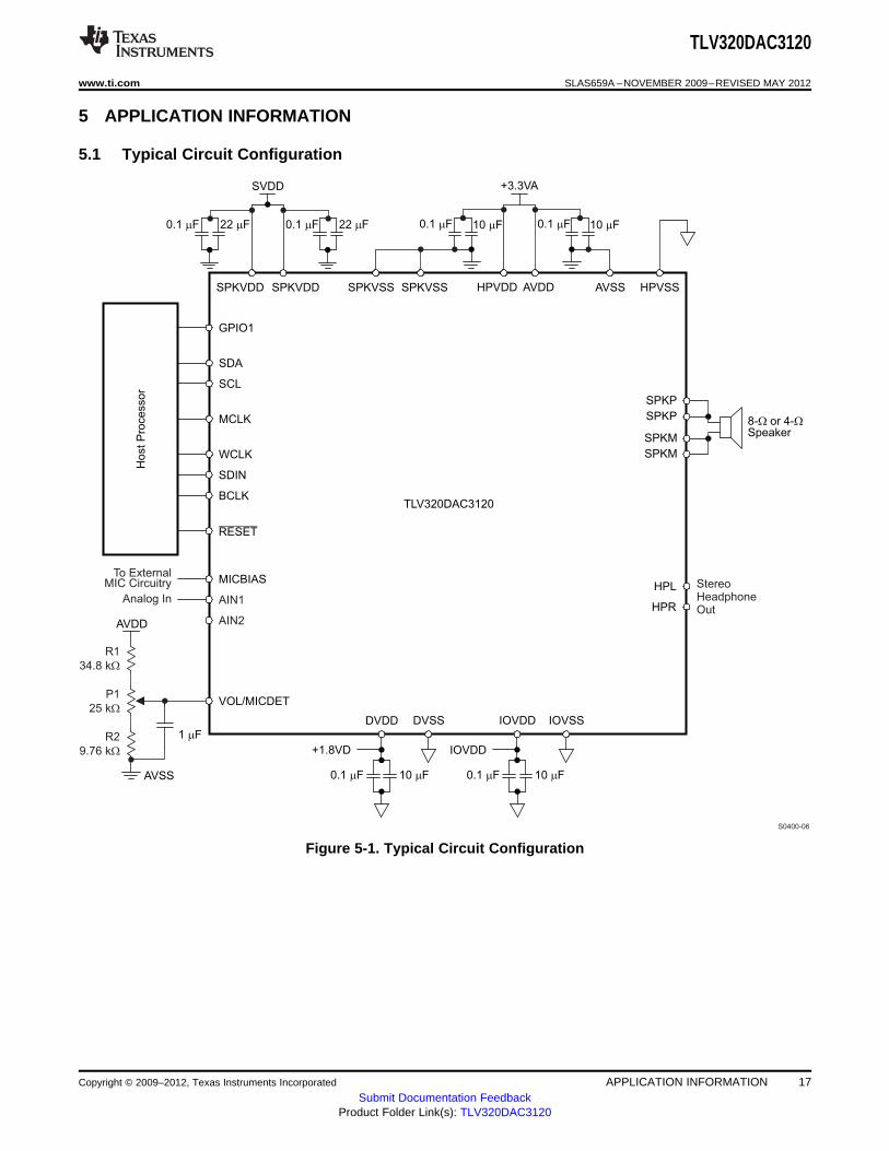
5.1 Typical Circuit Configuration
Figure 5-1. Typical Circuit Configuration
Copyright © 2009–2012, Texas Instruments Incorporated APPLICATION INFORMATION 17Submit Documentation Feedback
Product Folder Link(s): TLV320DAC3120
TLV320DAC3120
SLAS659A –NOVEMBER 2009–REVISED MAY 2012 www.ti.com
5.2 Overview
The TLV320DAC3120 is a highly integrated mono audio DAC for portable computing, communication, andentertainment applications. A register-based architecture eases integration with microprocessor-basedsystems through standard serial-interface buses. This device contains a two-wire I2C bus interface, whichallows full register access. All peripheral functions are controlled through these registers and the onboardstate machines.
The TLV320DAC3120 consists of the following blocks:• miniDSP digital signal-processing block• Audio DAC• Dynamic range compressor (DRC)• Mono headphone/lineout amplifier• Class-D mono amplifier capable of driving 4-Ω or 8-Ω speakers• Pin-controlled or register-controlled volume level• Power-down de-pop and power-up soft start• Analog inputs• I2C control interface• Power-down control block
Following a toggle of the RESET pin or a software reset, the device operates in the default mode. The I2Cinterface is used to write to the control registers to configure the device.
The I2C address assigned to the TLV320DAC3120 is 001 1000. This device always operates in an I2Cslave mode. All registers are 8-bit, and all writable registers have readback capability. The device auto-increments to support sequential addressing and can be used with I2C fast mode. Once the device isreset, all appropriate registers are updated by the host processor to configure the device as needed by theuser.
5.2.1 Device Initialization
5.2.1.1 Reset
The TLV320DAC3120 internal logic must be initialized to a known condition for proper device function. Toinitialize the device to its default operating condition, the hardware reset pin (RESET) must be pulled lowfor at least 10 ns. For this initialization to work, both the IOVDD and DVDD supplies must be powered up.It is recommended that while the DVDD supply is being powered up, the RESET pin be pulled low.
The device can also be reset via software reset. Writing a 1 into page 0 / register 1, bit D0 resets thedevice.
5.2.1.2 Device Start-Up Lockout Times
After the TLV320DAC3120 is initialized through hardware reset at power-up or software reset, the internalmemories are initialized to default values. This initialization takes place within 1 ms after pulling theRESET signal high. During this initialization phase, no register-read or register-write operation should beperformed on the DAC coefficient buffers. Also, no block within the codec should be powered up duringthe initialization phase.
5.2.1.3 PLL Start-Up
Whenever the PLL is powered up, a start-up delay of approximately of 10 ms occurs after the power-upcommand of the PLL and before the clocks are available to the codec. This delay is to ensure stableoperation of the PLL and clock-divider logic.
18 APPLICATION INFORMATION Copyright © 2009–2012, Texas Instruments Incorporated
Submit Documentation FeedbackProduct Folder Link(s): TLV320DAC3120
TLV320DAC3120
www.ti.com SLAS659A –NOVEMBER 2009–REVISED MAY 2012
5.2.1.4 Power-Stage Reset
The power-stage-only reset is used to reset the device after an overcurrent latching shutdown hasoccurred. Using this reset re-enables the output stage without resetting all of the registers in the device.Each of the two power stages has its own dedicated reset bit. The headphone power-stage reset isperformed by setting page 1 / register 31, bit D7 for HPOUT. The speaker power-stage reset is performedby setting page 1 / register 32, bit D7 for SPKP and SPKM.
5.2.1.5 Software Power Down
By default, all circuit blocks are powered down following a reset condition. Hardware power up of eachcircuit block can be controlled by writing to the appropriate control register. This approach allows thelowest power-supply current for the functionality required. However, when a block is powered down, all ofthe register settings are maintained as long as power is still being applied to the device.
5.2.2 Audio Analog I/O
The TLV320DAC3120 features a mono audio DAC. It supports a wide range of analog interfaces tosupport different headsets and analog outputs. The TLV320DAC3120 interfaces to output drivers (8-Ω, 16-Ω, 32-Ω).
5.3 miniDSP
The TLV320DAC3120 features a miniDSP core which is tightly coupled to the DAC. The fullyprogrammable algorithms for the miniDSP must be loaded into the device after power up. The miniDSPhas direct access to the digital stereo audio stream, offering the possibility for advanced, very low-group-delay DSP algorithms. The miniDSP has 1024 programmable instructions, 896 data memory locations,and 512 programmable coefficients (in the adaptive mode, each bank has 256 programmablecoefficients).
5.3.1 Software
Software development for the TLV320DAC3120 is supported through TI's comprehensive PurePath™Studio software development environment, a powerful, easy-to-use tool designed specifically to simplifysoftware development on Texas Instruments miniDSP audio platforms. The graphical developmentenvironment consists of a library of common audio functions that can be dragged and dropped into anaudio signal flow and graphically connected together. The DSP code can then be assembled from thegraphical signal flow with the click of a mouse. See the TLV320DAC3120 product folder on www.ti.com tolearn more about PurePath Studio and the latest status on available, ready-to-use DSP algorithms.
5.4 Digital Processing Low-Power Modes
The TLV320DAC3120 device can be tuned to minimize power dissipation, to maximize performance, or toan operating point between the two extremes to best fit the application. The choice of processing blocks,PRB_P4 to PRB_P22 for mono playback and PRB_R4 to PRB_R18 for mono recording, also influencesthe power consumption. In fact, the numerous processing blocks have been implemented to offer a choiceamong configurations having a different balance of power-optimization and signal-processing capabilities.
Copyright © 2009–2012, Texas Instruments Incorporated APPLICATION INFORMATION 19Submit Documentation Feedback
Product Folder Link(s): TLV320DAC3120
TLV320DAC3120
SLAS659A –NOVEMBER 2009–REVISED MAY 2012 www.ti.com
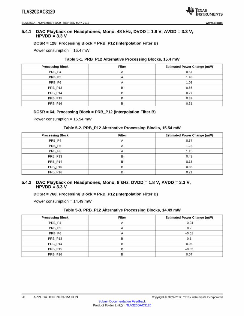
5.4.1 DAC Playback on Headphones, Mono, 48 kHz, DVDD = 1.8 V, AVDD = 3.3 V,HPVDD = 3.3 V
DOSR = 128, Processing Block = PRB_P12 (Interpolation Filter B)
Power consumption = 15.4 mW
Table 5-1. PRB_P12 Alternative Processing Blocks, 15.4 mW
Processing Block Filter Estimated Power Change (mW)
PRB_P4 A 0.57
PRB_P5 A 1.48
PRB_P6 A 1.08
PRB_P13 B 0.56
PRB_P14 B 0.27
PRB_P15 B 0.89
PRB_P16 B 0.31
DOSR = 64, Processing Block = PRB_P12 (Interpolation Filter B)
Power consumption = 15.54 mW
Table 5-2. PRB_P12 Alternative Processing Blocks, 15.54 mW
Processing Block Filter Estimated Power Change (mW)
PRB_P4 A 0.37
PRB_P5 A 1.23
PRB_P6 A 1.15
PRB_P13 B 0.43
PRB_P14 B 0.13
PRB_P15 B 0.85
PRB_P16 B 0.21
5.4.2 DAC Playback on Headphones, Mono, 8 kHz, DVDD = 1.8 V, AVDD = 3.3 V,HPVDD = 3.3 V
DOSR = 768, Processing Block = PRB_P12 (Interpolation Filter B)
Power consumption = 14.49 mW
Table 5-3. PRB_P12 Alternative Processing Blocks, 14.49 mW
Processing Block Filter Estimated Power Change (mW)
PRB_P4 A –0.04
PRB_P5 A 0.2
PRB_P6 A –0.01
PRB_P13 B 0.1
PRB_P14 B 0.05
PRB_P15 B –0.03
PRB_P16 B 0.07
20 APPLICATION INFORMATION Copyright © 2009–2012, Texas Instruments Incorporated
Submit Documentation FeedbackProduct Folder Link(s): TLV320DAC3120
TLV320DAC3120
www.ti.com SLAS659A –NOVEMBER 2009–REVISED MAY 2012
DOSR = 384, Processing Block = PRB_P12 (Interpolation Filter B)
Power consumption = 14.42 mW
Table 5-4. PRB_P12 Alternative Processing Blocks, 14.42 mW
Processing Block Filter Estimated Power Change (mW)
PRB_P4 A 0.16
PRB_P5 A 0.3
PRB_P6 A 0.2
PRB_P13 B 0.15
PRB_P14 B 0.07
PRB_P15 B 0.18
PRB_P16 B 0.09
5.5 Analog Signals
The TLV320DAC3120 analog signals consist of:• Microphone bias (MICBIAS)• Analog inputs AIN1 and AIN2, which can be used to pass-through or mix analog signals to output
stages• Analog outputs class-D speaker driver and headphone/lineout driver providing output capability for the
DAC, AIN1, AIN2, or a mix of the three
5.5.1 MICBIAS
The TLV320DAC3120 includes a microphone bias circuit which can source up to 4 mA of current, and isprogrammable to a 2-V, 2.5-V, or AVDD level. The level can be controlled by writing to page 1 /register 46, bits D1–D0. This functionality is shown in Table 5-5.
Table 5-5. MICBIAS Settings
D1 D0 FUNCTIONALITY
0 0 MICBIAS output is powered down.
0 1 MICBIAS output is powered to 2 V.
1 0 MICBIAS output is powered to 2.5 V.
1 1 MICBIAS output is powered to AVDD.
During normal operation, MICBIAS can be set to 2.5 V for better performance. However, depending on themodel of microphone that is selected, optimal performance might be obtained at another setting, so theperformance at a given setting should be verified.
The lowest current consumption occurs when MICBIAS is powered down. The next-lowest currentconsumption occurs when MICBIAS is set at AVDD.
5.5.2 Analog Inputs AIN1 and AIN2
AIN1 (pin 13) and AIN2 (pin 14) are inputs to the output mixer along with the DAC output. Page 1 /register 35 provides control signals for determining the signals routed through the output mixer. The outputof the output mixer then can be attenuated or amplified through the class-D and/or headphone/lineoutdrivers.
Copyright © 2009–2012, Texas Instruments Incorporated APPLICATION INFORMATION 21Submit Documentation Feedback
Product Folder Link(s): TLV320DAC3120
TLV320DAC3120
SLAS659A –NOVEMBER 2009–REVISED MAY 2012 www.ti.com
5.6 Audio DAC and Audio Analog Outputs
The mono audio DAC consists of a digital audio processing block, a digital interpolation filter, a digitaldelta-sigma modulator, and an analog reconstruction filter. The high oversampling ratio (normally DOSR isbetween 32 and 128) exhibits good dynamic range by ensuring that the quantization noise generatedwithin the delta-sigma modulator stays outside of the audio frequency band. Audio analog outputs includemono headphone/lineout and mono class-D speaker outputs. Because the TLV320DAC3120 contains amono DAC, it inputs the mono data from the left channel, the right channel, or a mix of the left and rightchannels as [(L + R) ÷ 2], selected by page 0 / register 63, bits D5–D4. See Figure 1-1 for the signal flow.
5.6.1 DAC
The TLV320DAC3120 mono audio DAC supports data rates from 8 kHz to 192 kHz. The audio channel ofthe mono DAC consists of a signal-processing engine with fixed processing blocks, a programmableminiDSP, a digital interpolation filter, multibit digital delta-sigma modulator, and an analog reconstructionfilter. The DAC is designed to provide enhanced performance at low sampling rates through increasedoversampling and image filtering, thereby keeping quantization noise generated within the delta-sigmamodulator and observed in the signal images strongly suppressed within the audio band to beyond 20kHz. To handle multiple input rates and optimize power dissipation and performance, theTLV320DAC3120 allows the system designer to program the oversampling rates over a wide range from 1to 1024 by configuring page 0 / register 13 and page 0 / register 14. The system designer can choosehigher oversampling ratios for lower input data rates and lower oversampling ratios for higher input datarates.
The TLV320DAC3120 DAC channel includes a built-in digital interpolation filter to generate oversampleddata for the delta-sigma modulator. The interpolation filter can be chosen from three different types,depending on required frequency response, group delay, and sampling rate.
DAC power up is controlled by writing to page 0 / register 63, bit D7 for the mono channel. The mono-channel DAC clipping flag is provided as a read-only bit on page 0 / register 39, bit D7.
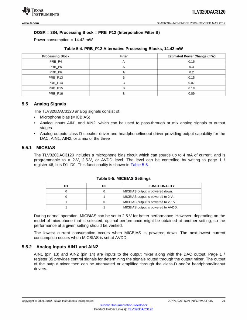
5.6.1.1 DAC Processing Blocks
The TLV320DAC3120 implements signal-processing capabilities and interpolation filtering via processingblocks. These fixed processing blocks give users the choice of how much and what type of signalprocessing they may use and which interpolation filter is applied.
The choices among these processing blocks allows the system designer to balance power conservationand signal-processing flexibility. Table 5-6 gives an overview of all available processing blocks of the DACchannel and their properties. The resource-class column gives an approximate indication of powerconsumption for the digital (DVDD) supply; however, based on the out-of-band noise spectrum, the analogpower consumption of the drivers (HPVDD) may differ.
The signal-processing blocks available are:• First-order IIR• Scalable number of biquad filters
The processing blocks are tuned for common cases and can achieve high image rejection or low groupdelay in combination with various signal-processing effects such as audio effects and frequency shaping.The available first-order IIR and biquad filters have fully user-programmable coefficients.
22 APPLICATION INFORMATION Copyright © 2009–2012, Texas Instruments Incorporated
Submit Documentation FeedbackProduct Folder Link(s): TLV320DAC3120
Interp.
Filter
A,B
BiQuad
F
BiQuad
E
BiQuad
D
BiQuad
C
BiQuad
B
BiQuad
AIIR to
Modulator
Digital
Volume
Ctrl
from
Interface
´
Interp.
Filter
A,B
DRCHPF
BiQuad
F
BiQuad
E
BiQuad
D
BiQuad
C
BiQuad
B
BiQuad
AIIR to
Modulator
Digital
Volume
Ctrl
from
Interface
´
Interp.
Filter A
BiQuad
C
BiQuad
B
BiQuad
Ato
Modulator
Digital
Volume
Ctrl
from
Interface
´
TLV320DAC3120
www.ti.com SLAS659A –NOVEMBER 2009–REVISED MAY 2012
Table 5-6. Overview – DAC Predefined Processing Blocks
Processing First-Order Number of ResourceInterpolation Filter Channel DRCBlock No. IIR Available Biquads Class
PRB_P4 A Mono No 3 No 4
PRB_P5 A Mono Yes 6 Yes 6
PRB_P6 A Mono Yes 6 No 6
PRB_P12 B Mono Yes 0 No 3
PRB_P13 B Mono No 4 Yes 4
PRB_P14 B Mono No 4 No 4
PRB_P15 B Mono Yes 6 Yes 6
PRB_P16 B Mono Yes 6 No 4
PRB_P20 C Mono Yes 0 No 2
PRB_P21 C Mono Yes 4 Yes 3
PRB_P22 C Mono Yes 4 No 2
PRB_P25 A Mono Yes 5 Yes 12
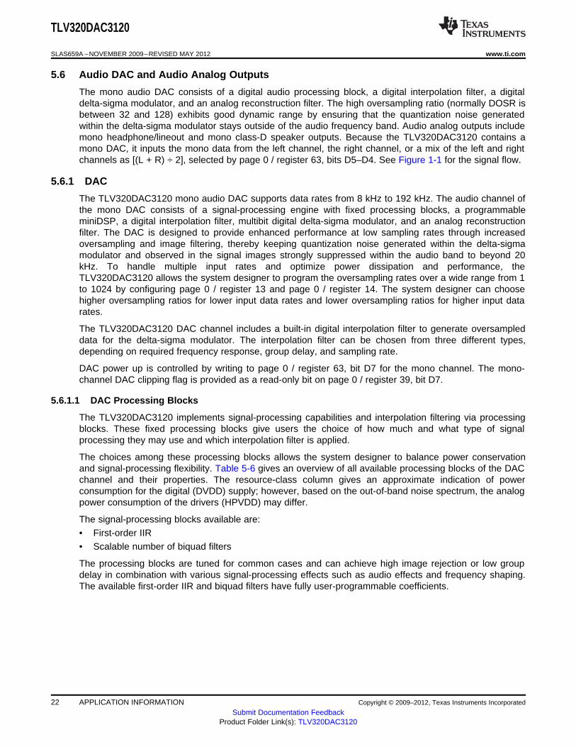
5.6.1.2 DAC Processing Blocks – Signal Chain Details
5.6.1.2.1 Three Biquads, Filter A
Figure 5-2. Signal Chain for PRB_P4
5.6.1.2.2 Six Biquads, First-Order IIR, DRC, Filter A or B
Figure 5-3. Signal Chain for PRB_P5 and PRB_P15
5.6.1.2.3 Six Biquads, First-Order IIR, Filter A or B
Figure 5-4. Signal Chain for PRB_P6 and PRB_P16
Copyright © 2009–2012, Texas Instruments Incorporated APPLICATION INFORMATION 23Submit Documentation Feedback
Product Folder Link(s): TLV320DAC3120
Interp.
Filter C
BiQuad
D
BiQuad
C
BiQuad
B
BiQuad
AIIR to
modulator
Digital
Volume
Ctrl
from
Interface
´
Interp.
Filter C
DRCHPF
IIR to
Modulator
Digital
Volume
Ctrl
BiQuad
D
BiQuad
C
BiQuad
B
BiQuad
A
from
Interface
´
Interp.
Filter B
BiQuad
D
BiQuad
C
BiQuad
B
BiQuad
Ato
Modulator
Digital
Volume
Ctrl
from
Interface
´
Interp.
Filter B
DRCHPF
to
Modulator
Digital
Volume
Ctrl
BiQuad
D
BiQuad
C
BiQuad
B
BiQuad
Afrom
Interface
´
Interp.
Filter
B,C
IIR to
Modulator
Digital
Volume
Ctrl
from
Interface
´
TLV320DAC3120
SLAS659A –NOVEMBER 2009–REVISED MAY 2012 www.ti.com
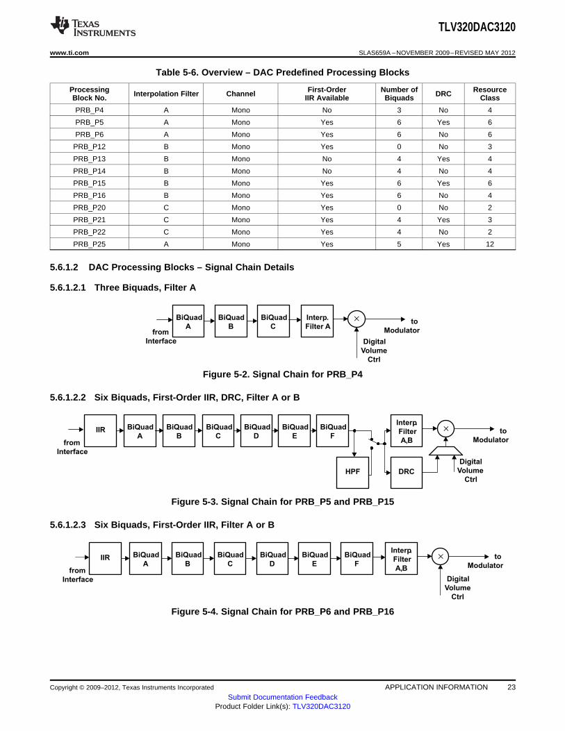
5.6.1.2.4 IIR, Filter B or C
Figure 5-5. Signal Chain for PRB_P12 and PRB_P20
5.6.1.2.5 Four Biquads, DRC, Filter B
Figure 5-6. Signal Chain for PRB_P13
5.6.1.2.6 Four Biquads, Filter B
Figure 5-7. Signal Chain for PRB_P14
5.6.1.2.7 Four Biquads, First-Order IIR, DRC, Filter C
Figure 5-8. Signal Chain for PRB_P21
5.6.1.2.8 Four Biquads, First-Order IIR, Filter C
Figure 5-9. Signal Chain for PRB_P22
24 APPLICATION INFORMATION Copyright © 2009–2012, Texas Instruments Incorporated
Submit Documentation FeedbackProduct Folder Link(s): TLV320DAC3120
DRCHPF
fromInterface
toModulator
DigitalVolume
Ctrl
BiQuadB ´
BiQuadC
BiQuadD
BiQuadE
BiQuadF
Interp.Filter A
+
BeepGen.
Beep Volume Ctrl ´
IIR
TLV320DAC3120
www.ti.com SLAS659A –NOVEMBER 2009–REVISED MAY 2012
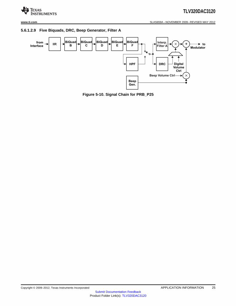
5.6.1.2.9 Five Biquads, DRC, Beep Generator, Filter A
Figure 5-10. Signal Chain for PRB_P25
Copyright © 2009–2012, Texas Instruments Incorporated APPLICATION INFORMATION 25Submit Documentation Feedback
Product Folder Link(s): TLV320DAC3120
Largest Positive Number:= 0.111 1111 1111 111= 0.999969482421875 = 1.0 – 1 LSB
1
Largest Negative Number:= 1.0000 0000 0000 000= 0x8000 = –1.0 (by definition)
1 1 1
1 1 1
S . xxxx xxxx xxxx xxx. . x x x
Sign Bit
2 Bit–1
2 Bit–4
2 Bit–15
FractionPoint
TLV320DAC3120
SLAS659A –NOVEMBER 2009–REVISED MAY 2012 www.ti.com
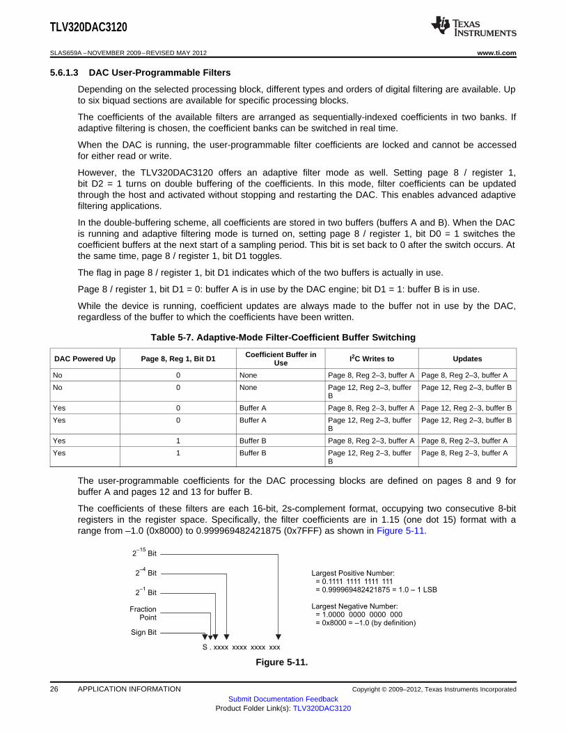
5.6.1.3 DAC User-Programmable Filters
Depending on the selected processing block, different types and orders of digital filtering are available. Upto six biquad sections are available for specific processing blocks.
The coefficients of the available filters are arranged as sequentially-indexed coefficients in two banks. Ifadaptive filtering is chosen, the coefficient banks can be switched in real time.
When the DAC is running, the user-programmable filter coefficients are locked and cannot be accessedfor either read or write.
However, the TLV320DAC3120 offers an adaptive filter mode as well. Setting page 8 / register 1,bit D2 = 1 turns on double buffering of the coefficients. In this mode, filter coefficients can be updatedthrough the host and activated without stopping and restarting the DAC. This enables advanced adaptivefiltering applications.
In the double-buffering scheme, all coefficients are stored in two buffers (buffers A and B). When the DACis running and adaptive filtering mode is turned on, setting page 8 / register 1, bit D0 = 1 switches thecoefficient buffers at the next start of a sampling period. This bit is set back to 0 after the switch occurs. Atthe same time, page 8 / register 1, bit D1 toggles.
The flag in page 8 / register 1, bit D1 indicates which of the two buffers is actually in use.
Page 8 / register 1, bit D1 = 0: buffer A is in use by the DAC engine; bit D1 = 1: buffer B is in use.
While the device is running, coefficient updates are always made to the buffer not in use by the DAC,regardless of the buffer to which the coefficients have been written.
Table 5-7. Adaptive-Mode Filter-Coefficient Buffer Switching
Coefficient Buffer inDAC Powered Up Page 8, Reg 1, Bit D1 I2C Writes to UpdatesUse
No 0 None Page 8, Reg 2–3, buffer A Page 8, Reg 2–3, buffer A
No 0 None Page 12, Reg 2–3, buffer Page 12, Reg 2–3, buffer BB
Yes 0 Buffer A Page 8, Reg 2–3, buffer A Page 12, Reg 2–3, buffer B
Yes 0 Buffer A Page 12, Reg 2–3, buffer Page 12, Reg 2–3, buffer BB
Yes 1 Buffer B Page 8, Reg 2–3, buffer A Page 8, Reg 2–3, buffer A
Yes 1 Buffer B Page 12, Reg 2–3, buffer Page 8, Reg 2–3, buffer AB
The user-programmable coefficients for the DAC processing blocks are defined on pages 8 and 9 forbuffer A and pages 12 and 13 for buffer B.
The coefficients of these filters are each 16-bit, 2s-complement format, occupying two consecutive 8-bitregisters in the register space. Specifically, the filter coefficients are in 1.15 (one dot 15) format with arange from –1.0 (0x8000) to 0.999969482421875 (0x7FFF) as shown in Figure 5-11.
Figure 5-11.
26 APPLICATION INFORMATION Copyright © 2009–2012, Texas Instruments Incorporated
Submit Documentation FeedbackProduct Folder Link(s): TLV320DAC3120
1 20 1 2
15 1 21 2
N 2 N z N zH(z)
2 2 D z D z
- -
- -
+ ´ +
=
- ´ -
10 1
15 11
N N zH(z)
2 D z
-
-
+
=
-
TLV320DAC3120
www.ti.com SLAS659A –NOVEMBER 2009–REVISED MAY 2012
5.6.1.3.1 First-Order IIR Section
The IIR is of first order and its transfer function is given by
(1)
The frequency response for the first-order IIR section with default coefficients is flat.
Table 5-8. DAC IIR Filter Coefficients
DAC Coefficient,Filter Filter Coefficient Default (Reset) ValuesMono Channel
First-order IIR N0 Page 9 / registers 2–3 0x7FFF (decimal 1.0 – LSB value)
N1 Page 9 / registers 4–5 0x0000
D1 Page 9 / registers 6–7 0x0000
5.6.1.3.2 Biquad Section
The transfer function of each of the biquad filters is given by
(2)
Table 5-9. DAC Biquad Filter Coefficients
Filter Coefficient Mono DAC Channel Default (Reset) Values
Biquad A N0 Page 8 / registers 2–3 0x7FFF (decimal 1.0 – LSB value)
N1 Page 8 / registers 4–5 0x0000
N2 Page 8 / registers 6–7 0x0000
D1 Page 8 / registers 8–9 0x0000
D2 Page 8 / registers 10–11 0x0000
Biquad B N0 Page 8 / registers 12–13 0x7FFF (decimal 1.0 – LSB value)
N1 Page 8 / registers 14–15 0x0000
N2 Page 8 / registers 16–17 0x0000
D1 Page 8 / registers 18–19 0x0000
D2 Page 8 / registers 20–21 0x0000
Biquad C N0 Page 8 / registers 22–23 0x7FFF (decimal 1.0 – LSB value)
N1 Page 8 / registers 24–25 0x0000
N2 Page 8 / registers 26–27 0x0000
D1 Page 8 / registers 28–29 0x0000
D2 Page 8 / registers 30–31 0x0000
Biquad D N0 Page 8 / registers 32–33 0x7FFF (decimal 1.0 – LSB value)
N1 Page 8 / registers 34–35 0x0000
N2 Page 8 / registers 36–37 0x0000
D1 Page 8 / registers 38–39 0x0000
D2 Page 8 / registers 40–41 0x0000
Biquad E N0 Page 8 / registers 42–43 0x7FFF (decimal 1.0 – LSB value)
N1 Page 8 / registers 44–45 0x0000
N2 Page 8 / registers 46–47 0x0000
D1 Page 8 / registers 48–49 0x0000
D2 Page 8 / registers 50–51 0x0000
Copyright © 2009–2012, Texas Instruments Incorporated APPLICATION INFORMATION 27Submit Documentation Feedback
Product Folder Link(s): TLV320DAC3120
0
–10
–20
–30
–40
–50
–60
–70
–80
–90
1 3 4 5 6 72
Mag
nit
ud
e–
dB
Frequency Normalized to fS
DAC Channel Response for Interpolation Filter A(Red Line Corresponds to –65 dB)
TLV320DAC3120
SLAS659A –NOVEMBER 2009–REVISED MAY 2012 www.ti.com
Table 5-9. DAC Biquad Filter Coefficients (continued)
Filter Coefficient Mono DAC Channel Default (Reset) Values
Biquad F N0 Page 8 / registers 52–53 0x7FFF (decimal 1.0 – LSB value)
N1 Page 8 / registers 54–55 0x0000
N2 Page 8 / registers 56–57 0x0000
D1 Page 8 / registers 58–59 0x0000
D2 Page 8 / registers 60–61 0x0000
5.6.1.4 DAC Interpolation Filter Characteristics
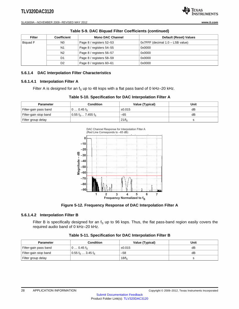
5.6.1.4.1 Interpolation Filter A
Filter A is designed for an fS up to 48 ksps with a flat pass band of 0 kHz–20 kHz.
Table 5-10. Specification for DAC Interpolation Filter A
Parameter Condition Value (Typical) Unit
Filter-gain pass band 0 … 0.45 fS ±0.015 dB
Filter-gain stop band 0.55 fS… 7.455 fS –65 dB
Filter group delay 21/fS s
Figure 5-12. Frequency Response of DAC Interpolation Filter A
5.6.1.4.2 Interpolation Filter B
Filter B is specifically designed for an fS up to 96 ksps. Thus, the flat pass-band region easily covers therequired audio band of 0 kHz–20 kHz.
Table 5-11. Specification for DAC Interpolation Filter B
Parameter Condition Value (Typical) Unit
Filter-gain pass band 0 … 0.45 fS ±0.015 dB
Filter-gain stop band 0.55 fS … 3.45 fS –58 dB
Filter group delay 18/fS s
28 APPLICATION INFORMATION Copyright © 2009–2012, Texas Instruments Incorporated
Submit Documentation FeedbackProduct Folder Link(s): TLV320DAC3120
0
–10
–20
–30
–40
–50
–60
–70
Mag
nit
ud
e–
dB
0 0.2 0.4 0.6 0.8 1 1.2 1.4
Frequency Normalized to fS
DAC Channel Response for Interpolation Filter C(Red Line Corresponds to –43 dB)
DAC Channel Response for Interpolation Filter B(Red Line Corresponds to –58 dB)
0.5 1 1.5 2 2.5 3 3.5Frequency Normalized to fS
0
–10
–20
–30
–40
–50
–60
–70
–80
Mag
nit
ud
e–
dB
TLV320DAC3120
www.ti.com SLAS659A –NOVEMBER 2009–REVISED MAY 2012
Figure 5-13. Frequency Response of Channel Interpolation Filter B
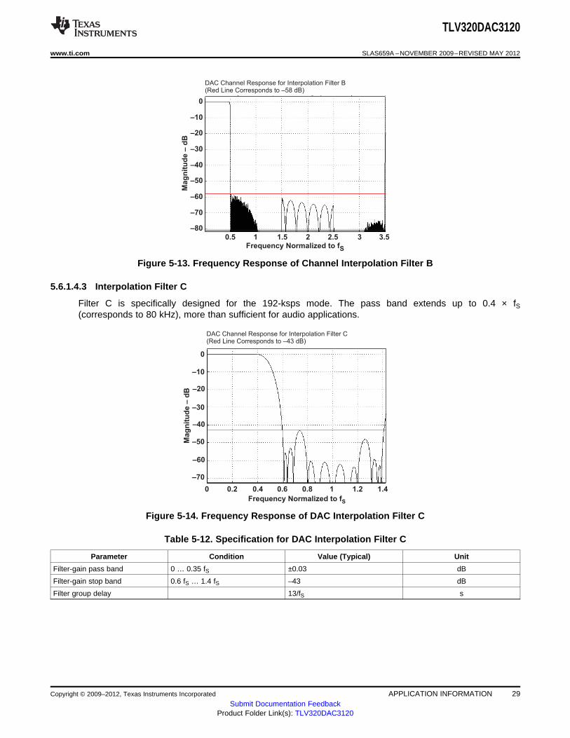
5.6.1.4.3 Interpolation Filter C
Filter C is specifically designed for the 192-ksps mode. The pass band extends up to 0.4 × fS(corresponds to 80 kHz), more than sufficient for audio applications.
Figure 5-14. Frequency Response of DAC Interpolation Filter C
Table 5-12. Specification for DAC Interpolation Filter C
Parameter Condition Value (Typical) Unit
Filter-gain pass band 0 … 0.35 fS ±0.03 dB
Filter-gain stop band 0.6 fS … 1.4 fS –43 dB
Filter group delay 13/fS s
Copyright © 2009–2012, Texas Instruments Incorporated APPLICATION INFORMATION 29Submit Documentation Feedback
Product Folder Link(s): TLV320DAC3120
TLV320DAC3120
SLAS659A –NOVEMBER 2009–REVISED MAY 2012 www.ti.com
5.6.2 DAC Digital-Volume Control
The DAC has a digital volume-control block which implements programmable gain. Each channel has anindependent volume control that can be varied from 24 dB to –63.5 dB in 0.5-dB steps. The mono-channelDAC volume can be controlled by writing to page 0 / register 65, bits D7–D0. DAC muting and setting up amaster gain control to control the mono channel is done by writing to page 0 / register 64, bits D3 and D1.The gain is implemented with a soft-stepping algorithm, which only changes the actual volume by0.125 dB per input sample, either up or down, until the desired volume is reached. The rate of soft-stepping can be slowed to one step per two input samples by writing to page 0 / register 63, bits D1–D0.Note that the default source for volume-control level settings is controlled by register writes to page 0 /register 65. Use of the VOL/MICDET pin to control the DAC volume is ignored until the volume-controlsource selected has been changed to pin control (page 0 / register 116, bit D7 = 1). This functionality isshown in Figure 1-1.
During soft-stepping, the host does not receive a signal when the DAC has been completely muted. Thismay be important if the host must mute the DAC before making a significant change, such as changingsample rates. In order to help with this situation, the device provides a flag back to the host via a read-only register, page 0 / register 38, bit D4 for the mono channel. This information alerts the host when thepart has completed the soft-stepping, and the actual volume has reached the desired volume level. Thesoft-stepping feature can be disabled by writing to page 0 / register 63, bits D1–D0.
If soft-stepping is enabled, the CODEC_CLKIN signal should be kept active until the DAC power-up flag iscleared. When this flag is cleared, the internal DAC soft-stepping process is complete, andCODEC_CLKIN can be stopped if desired. (The analog volume control can be ramped down using aninternal oscillator.)
5.6.3 Volume-Control Pin
The range of voltages used by the 7-bit SAR ADC is shown in the Electrical Characteristics table.
The volume-control pin is not enabled by default, but it can be enabled by writing 1 to page 0 /register 116, bit D7. The default DAC volume control uses software control of the volume, which occurs ifpage 0 / register 116, bit D7 = 0. Soft-stepping the volume level is set up by writing to page 0 / register 63,bits D1–D0.
When the volume-pin function is used, a 7-bit Vol ADC reads the voltage on the VOL/MICDET pin andupdates the digital volume control. (It overwrites the current value of the volume control.) The new volumesetting which has been applied due to a change of voltage on the volume control pin can be read onpage 0 / register 117, bits D6–D0. The 7-bit Vol ADC clock source can be selected on page 0 /register 116, bit D6. The update rate can be programmed on page 0 / register 116, bits D2–D0 for this 7-bit SAR ADC.
The VOL/MICDET pin gain mapping is shown in Table 5-13.
Table 5-13. VOL/MICDET Pin Gain Mapping
VOL/MICDET PIN SAR OUTPUT DIGITAL GAIN APPLIED
0 18 dB
1 17.5 dB
2 17 dB
: :
35 0.5 dB
36 0.0 dB
37 –0.5 dB
: :
89 –26.5 dB
30 APPLICATION INFORMATION Copyright © 2009–2012, Texas Instruments Incorporated
Submit Documentation FeedbackProduct Folder Link(s): TLV320DAC3120
10 1
HPF 15 11
N N zH (z)
2 D z
-
-
+
=
-
TLV320DAC3120
www.ti.com SLAS659A –NOVEMBER 2009–REVISED MAY 2012
Table 5-13. VOL/MICDET Pin Gain Mapping (continued)
VOL/MICDET PIN SAR OUTPUT DIGITAL GAIN APPLIED
90 –27 dB
91 –28 dB
: :
125 –62 dB
126 –63 dB
127 Mute
The VOL/MICDET pin connection and functionality are shown in Figure 1-1.
As shown in Table 5-13, the VOL/MICDET pin has a range of volume control from 18 dB down to –63 dB,and mute. However, if less maximum gain is required, then a smaller range of voltage should be appliedto the VOL/MICDET pin. This can be done by increasing the value of R2 relative to the value of (P1 + R1),so that more voltage is available at the bottom of P1. The circuit should also be designed such that for thevalues of R1, R2, and P1 chosen, the maximum voltage (top of the potentiometer) does not exceedAVDD/2 (see Figure 5-1). The recommended values for R1, R2, and P1 for several maximum gains areshown in Table 5-14. Note that In typical applications, R1 should not be 0 Ω, as the VOL/MICDET pinshould not exceed AVDD/2 for proper ADC operation.
Table 5-14. VOL/MICDET Pin Gain Scaling
ADC VOLTAGER1 P1 R2 DIGITAL GAIN RANGEfor AVDD = 3.3 V(kΩ) (kΩ) (kΩ) (dB)(V)
25 25 0 0 V to 1.65 V 18 dB to –63 dB
33 25 7.68 0.386 V to 1.642 V 3 dB to –63 dB
34.8 25 9.76 0.463 V to 1.649 V 0 dB to –63 dB
5.6.4 Dynamic Range Compression
Typical music signals are characterized by crest factors, the ratio of peak signal power to average signalpower, of 12 dB or more. To avoid audible distortions due to clipping of peak signals, the gain of the DACchannel must be adjusted so as not to cause hard clipping of peak signals. As a result, during nominalperiods, the applied gain is low, causing the perception that the signal is not loud enough. To overcomethis problem, DRC in the TLV320DAC3120 continuously monitors the output of the DAC digital volumecontrol to detect its power level relative to 0 dBFS. When the power level is low, DRC increases the inputsignal gain to make it sound louder. At the same time, if a peaking signal is detected, it autonomouslyreduces the applied gain to avoid hard clipping. This results in sounds more pleasing to the ear as well assounding louder during nominal periods.
The DRC functionality in the TLV320DAC3120 is implemented by a combination of processing blocks inthe DAC channel as described in Section 5.6.1.2.
DRC can be disabled by writing to page 0 / register 68, bits D6–D5.
DRC typically works on the filtered version of the input signal. The input signals have no audio informationat dc and extremely low frequencies; however, they can significantly influence the energy estimationfunction in DRC. Also, most of the information about signal energy is concentrated in the low-frequencyregion of the input signal.
To estimate the energy of the input signal, the signal is first fed to the DRC high-pass filter and then to theDRC low-pass filter. These filters are implemented as first-order IIR filters given by
(3)
Copyright © 2009–2012, Texas Instruments Incorporated APPLICATION INFORMATION 31Submit Documentation Feedback
Product Folder Link(s): TLV320DAC3120
10 1
LPF 15 11
N N zH (z)
2 D z
-
-
+
=
-
TLV320DAC3120
SLAS659A –NOVEMBER 2009–REVISED MAY 2012 www.ti.com
(4)
The coefficients for these filters are 16 bits wide in 2s-complement format and are user-programmablethrough register write as given in Table 5-15.
32 APPLICATION INFORMATION Copyright © 2009–2012, Texas Instruments Incorporated
Submit Documentation FeedbackProduct Folder Link(s): TLV320DAC3120
TLV320DAC3120
www.ti.com SLAS659A –NOVEMBER 2009–REVISED MAY 2012
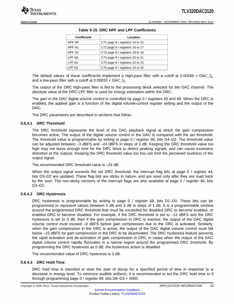
Table 5-15. DRC HPF and LPF Coefficients
Coefficient Location
HPF N0 C71 page 9 / registers 14 to 15
HPF N1 C72 page 9 / registers 16 to 17
HPF D1 C73 page 9 / registers 18 to 19
LPF N0 C74 page 9 / registers 20 to 21
LPF N1 C75 page 9 / registers 22 to 23
LPF D1 C76 page 9 / registers 24 to 25
The default values of these coefficients implement a high-pass filter with a cutoff at 0.00166 × DAC_fS,and a low-pass filter with a cutoff at 0.00033 × DAC_fS.
The output of the DRC high-pass filter is fed to the processing block selected for the DAC channel. Theabsolute value of the DRC-LPF filter is used for energy estimation within the DRC.
The gain in the DAC digital volume control is controlled by page 0 / registers 65 and 66. When the DRC isenabled, the applied gain is a function of the digital volume-control register setting and the output of theDRC.
The DRC parameters are described in sections that follow.
5.6.4.1 DRC Threshold
The DRC threshold represents the level of the DAC playback signal at which the gain compressionbecomes active. The output of the digital volume control in the DAC is compared with the set threshold.The threshold value is programmable by writing to page 0 / register 68, bits D4–D2. The threshold valuecan be adjusted between –3 dBFS and –24 dBFS in steps of 3 dB. Keeping the DRC threshold value toohigh may not leave enough time for the DRC block to detect peaking signals, and can cause excessivedistortion at the outputs. Keeping the DRC threshold value too low can limit the perceived loudness of theoutput signal.
The recommended DRC threshold value is –24 dB.
When the output signal exceeds the set DRC threshold, the interrupt flag bits at page 0 / register 44,bits D3–D2 are updated. These flag bits are sticky in nature, and are reset only after they are read backby the user. The non-sticky versions of the interrupt flags are also available at page 0 / register 46, bitsD3–D2.
5.6.4.2 DRC Hysteresis
DRC hysteresis is programmable by writing to page 0 / register 68, bits D1–D0. These bits can beprogrammed to represent values between 0 dB and 3 dB in steps of 1 dB. It is a programmable windowaround the programmed DRC threshold that must be exceeded for disabled DRC to become enabled, orenabled DRC to become disabled. For example, if the DRC threshold is set to –12 dBFS and the DRChysteresis is set to 3 dB, then if the gain compression in DRC is inactive, the output of the DAC digitalvolume control must exceed –9 dBFS before gain compression due to the DRC is activated. Similarly,when the gain compression in the DRC is active, the output of the DAC digital volume control must fallbelow –15 dBFS for gain compression in the DRC to be deactivated. The DRC hysteresis feature preventsthe rapid activation and de-activation of gain compression in DRC in cases when the output of the DACdigital volume control rapidly fluctuates in a narrow region around the programmed DRC threshold. Byprogramming the DRC hysteresis as 0 dB, the hysteresis action is disabled.
The recommended value of DRC hysteresis is 3 dB.
5.6.4.3 DRC Hold Time
DRC hold time is intended to slow the start of decay for a specified period of time in response to adecrease in energy level. To minimize audible artifacts, it is recommended to set the DRC hold time to 0through programming page 0 / register 69, bits D6–D3 = 0000.
Copyright © 2009–2012, Texas Instruments Incorporated APPLICATION INFORMATION 33Submit Documentation Feedback
Product Folder Link(s): TLV320DAC3120
TLV320DAC3120
SLAS659A –NOVEMBER 2009–REVISED MAY 2012 www.ti.com
5.6.4.4 DRC Attack Rate
When the output of the DAC digital volume control exceeds the programmed DRC threshold, the gainapplied in the DAC digital volume control is progressively reduced to prevent the signal from saturating thechannel. This process of reducing the applied gain is called attack. To avoid audible artifacts, the gain isreduced slowly with a rate equaling the attack rate, programmable via page 0 / register 70, bits D7–D4.Attack rates can be programmed from 4-dB gain change per sample period to 1.2207e–5-dB gain changeper sample period.
Attack rates should be programmed such that before the output of the DAC digital volume control can clip,the input signal should be sufficiently attenuated. High attack rates can cause audible artifacts, and too-slow attack rates may not be able to prevent the input signal from clipping.
The recommended DRC attack rate value is 1.9531e–4 dB per sample period.
5.6.4.5 DRC Decay Rate
When the DRC detects a reduction in output signal swing beyond the programmed DRC threshold, theDRC enters a decay state, where the applied gain in the digital-volume control is gradually increased toprogrammed values. To avoid audible artifacts, the gain is slowly increased with a rate equal to the decayrate programmed through page 0 / register 70, bits D3–D0. The decay rates can be programmed from1.5625e–3 dB per sample period to 4.7683e–7 dB per sample period. If the decay rates are programmedtoo high, then sudden gain changes can cause audible artifacts. However, if it is programmed too slow,then the output may be perceived as too low for a long time after the peak signal has passed.
The recommended Value of DRC attack rate is 2.4414e–5 dB per sample period.
5.6.4.6 Example Setup for DRC
• DAC vol gain = 12 dB• Threshold = –24 dB• Hysteresis = 3 dB• Hold time = 0 ms• Attack rate = 1.9531e–4 dB per sample period• Decay rate = 2.4414e–5 dB per sample period
Script#Go to Page 0 w 30 00 00 #DAC => 12 db gain mono w 30 41 18 #DAC => DRC Enabled, Threshold = -24 db, Hysteresis = 3 dB w 30 44 7F #DRC Hold = 0 ms, Rate of Changes of Gain = 0.5 dB/Fs' w 3045 00 #Attack Rate = 1.9531e-4 dB/Frame , DRC Decay Rate =2.4414e-5 dB/Frame w 30 46 B6 #Go to Page 9 w 30 00 09 #DRC HPF w 30 0E 7F AB 80 55 7F 56 #DRC LPF W 3014 00 11 00 11 7F DE
5.6.4.7 Headset Detection
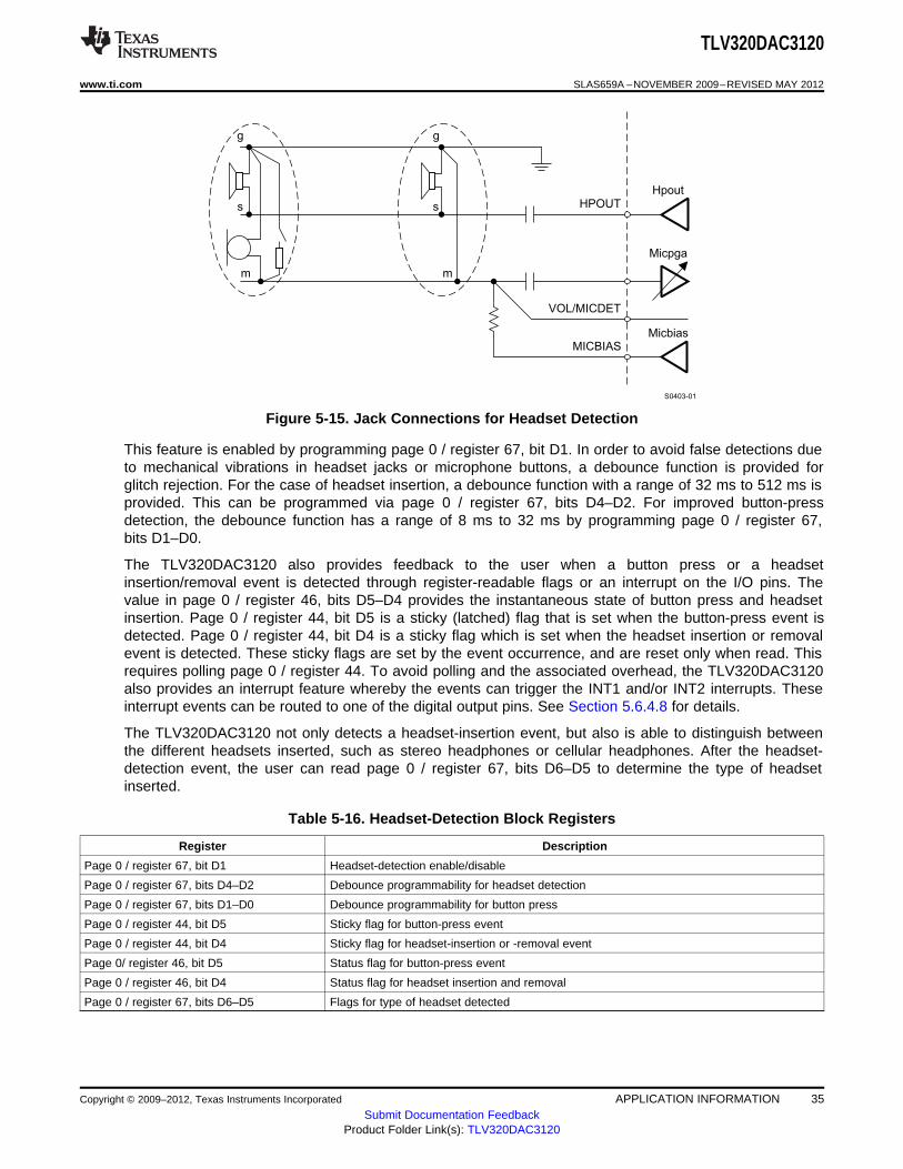
The TLV320DAC3120 includes extensive capability to monitor a headphone, microphone, or headset jack,to determine if a plug has been inserted into the jack, and then determine what type ofheadset/headphone is wired to the plug. The device also includes the capability to detect a button press,even, for example, when starting calls on mobile phones with headsets. Figure 5-15 shows the circuitconfiguration to enable this feature.
34 APPLICATION INFORMATION Copyright © 2009–2012, Texas Instruments Incorporated
Submit Documentation FeedbackProduct Folder Link(s): TLV320DAC3120
g
s
m
Micbias
m
s
g
MICBIAS
HPOUT
VOL/MICDET
Micpga
Hpout
S0403-01
TLV320DAC3120
www.ti.com SLAS659A –NOVEMBER 2009–REVISED MAY 2012
Figure 5-15. Jack Connections for Headset Detection
This feature is enabled by programming page 0 / register 67, bit D1. In order to avoid false detections dueto mechanical vibrations in headset jacks or microphone buttons, a debounce function is provided forglitch rejection. For the case of headset insertion, a debounce function with a range of 32 ms to 512 ms isprovided. This can be programmed via page 0 / register 67, bits D4–D2. For improved button-pressdetection, the debounce function has a range of 8 ms to 32 ms by programming page 0 / register 67,bits D1–D0.
The TLV320DAC3120 also provides feedback to the user when a button press or a headsetinsertion/removal event is detected through register-readable flags or an interrupt on the I/O pins. Thevalue in page 0 / register 46, bits D5–D4 provides the instantaneous state of button press and headsetinsertion. Page 0 / register 44, bit D5 is a sticky (latched) flag that is set when the button-press event isdetected. Page 0 / register 44, bit D4 is a sticky flag which is set when the headset insertion or removalevent is detected. These sticky flags are set by the event occurrence, and are reset only when read. Thisrequires polling page 0 / register 44. To avoid polling and the associated overhead, the TLV320DAC3120also provides an interrupt feature whereby the events can trigger the INT1 and/or INT2 interrupts. Theseinterrupt events can be routed to one of the digital output pins. See Section 5.6.4.8 for details.
The TLV320DAC3120 not only detects a headset-insertion event, but also is able to distinguish betweenthe different headsets inserted, such as stereo headphones or cellular headphones. After the headset-detection event, the user can read page 0 / register 67, bits D6–D5 to determine the type of headsetinserted.
Table 5-16. Headset-Detection Block Registers
Register Description
Page 0 / register 67, bit D1 Headset-detection enable/disable
Page 0 / register 67, bits D4–D2 Debounce programmability for headset detection
Page 0 / register 67, bits D1–D0 Debounce programmability for button press
Page 0 / register 44, bit D5 Sticky flag for button-press event
Page 0 / register 44, bit D4 Sticky flag for headset-insertion or -removal event
Page 0/ register 46, bit D5 Status flag for button-press event
Page 0 / register 46, bit D4 Status flag for headset insertion and removal
Page 0 / register 67, bits D6–D5 Flags for type of headset detected
Copyright © 2009–2012, Texas Instruments Incorporated APPLICATION INFORMATION 35Submit Documentation Feedback
Product Folder Link(s): TLV320DAC3120
TLV320DAC3120
SLAS659A –NOVEMBER 2009–REVISED MAY 2012 www.ti.com
The headset detection block requires AVDD to be powered. The headset-detection feature in theTLV320DAC3120 is achieved with very low power overhead, requiring less than 20 μA of additionalcurrent from the AVDD supply.
5.6.4.8 Interrupts
Some specific events in the TLV320DAC3120, which may require host-processor intervention, can beused to trigger interrupts to the host processor. This avoids polling the status-flag registers continuously.The TLV320DAC3120 has two defined interrupts, INT1 and INT2, that can be configured by programmingpage 0 / register 48 and page 0 / register 49. A user can configure interrupts INT1 and INT2 to betriggered by one or many events, such as:• Headset detection• Button press• DAC DRC signal exceeding threshold• Noise detected by AGC• Overcurrent condition in headphone drivers/speaker drivers• Data overflow in the DAC processing blocks and filters• DC measurement data available
Each of these INT1 and INT2 interrupts can be routed to output pin GPIO1. These interrupt signals caneither be configured as a single pulse or a series of pulses by programming page 0 / register 48, bit D0and page 0 / register 49, bit D0. If the user configures the interrupts as a series of pulses, the eventstrigger the start of pulses that stop when the flag registers in page 0 / register 44, page 0 / register 45, andpage 0 / register 50 are read by the user to determine the cause of the interrupt.
5.6.5 Key-Click Functionality With Beep Generator (PRB_P25)
A special algorithm has been included in the digital signal processing block PRB_P25 for generating adigital sine-wave signal that is sent to the DAC. This functionality is intended for generating key-clicksounds for user feedback. The sine-wave generator is very flexible (see Table 5-17) and is completelyregister programmable. Programming page 0 / register 71 through page 0 / register 79 (8 bits each)completely controls the functionality of this generator and allows for differentiating sounds.
The two registers used for programming the 16-bit sine-wave coefficient are page 0 / register 76 andpage 0 / register 77. The two registers used for programming the 16-bit cosine-wave coefficient arepage 0 / register 78 and page 0 / register 79. This coefficient resolution allows virtually any frequency ofsine wave in the audio band to be generated, up to fS/2.
The three registers used to control the length of the sine-burst waveform are page 0 / register 73 throughpage 0 / register 75. The resolution (bit) in the registers of the sine-burst length is one sample time, so thisallows great control on the overall time of the sine-burst waveform. This 24-bit length timer supports16,777,215 sample times. (For example, if fS is set at 48 kHz, and the register value equals 96,000d(01 7700h), then the sine burst lasts exactly 2 seconds.) The default settings for the tone generator, basedon using a sample rate of 48 kHz, are 1-kHz (approximately) sine wave, with a sine-burst length of fivecycles (5 ms).
Table 5-17. Beep Generator Register Locations (Page 00h)
BEEP LENGTH SINE COSINELEFT BEEP CONTROL RIGHT BEEP CONTROL
MSB MID LSB MSB LSB MSB LSB
REGISTER 71 72 73 74 75 76 77 78 79
36 APPLICATION INFORMATION Copyright © 2009–2012, Texas Instruments Incorporated
Submit Documentation FeedbackProduct Folder Link(s): TLV320DAC3120
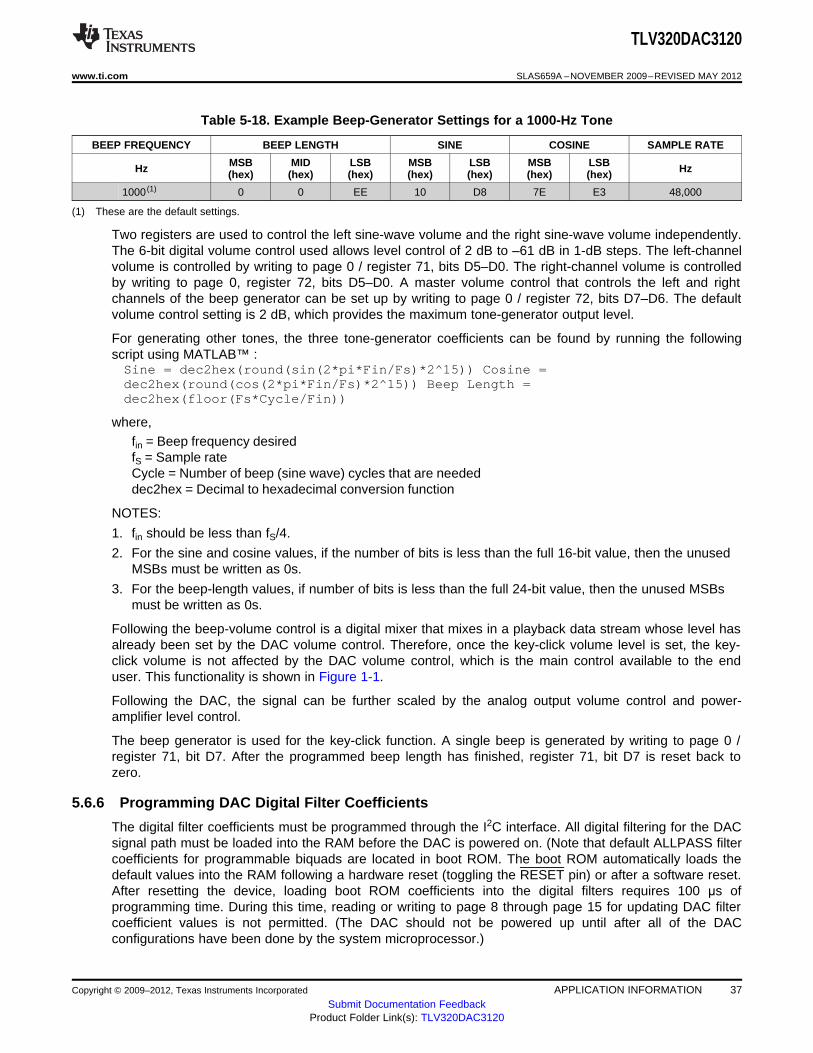
TLV320DAC3120
www.ti.com SLAS659A –NOVEMBER 2009–REVISED MAY 2012
Table 5-18. Example Beep-Generator Settings for a 1000-Hz Tone
BEEP FREQUENCY BEEP LENGTH SINE COSINE SAMPLE RATE
MSB MID LSB MSB LSB MSB LSBHz Hz(hex) (hex) (hex) (hex) (hex) (hex) (hex)
1000 (1) 0 0 EE 10 D8 7E E3 48,000
(1) These are the default settings.
Two registers are used to control the left sine-wave volume and the right sine-wave volume independently.The 6-bit digital volume control used allows level control of 2 dB to –61 dB in 1-dB steps. The left-channelvolume is controlled by writing to page 0 / register 71, bits D5–D0. The right-channel volume is controlledby writing to page 0, register 72, bits D5–D0. A master volume control that controls the left and rightchannels of the beep generator can be set up by writing to page 0 / register 72, bits D7–D6. The defaultvolume control setting is 2 dB, which provides the maximum tone-generator output level.
For generating other tones, the three tone-generator coefficients can be found by running the followingscript using MATLAB™ :Sine = dec2hex(round(sin(2*pi*Fin/Fs)*2^15)) Cosine =dec2hex(round(cos(2*pi*Fin/Fs)*2^15)) Beep Length =dec2hex(floor(Fs*Cycle/Fin))
where,fin = Beep frequency desiredfS = Sample rateCycle = Number of beep (sine wave) cycles that are neededdec2hex = Decimal to hexadecimal conversion function
NOTES:
1. fin should be less than fS/4.
2. For the sine and cosine values, if the number of bits is less than the full 16-bit value, then the unusedMSBs must be written as 0s.
3. For the beep-length values, if number of bits is less than the full 24-bit value, then the unused MSBsmust be written as 0s.
Following the beep-volume control is a digital mixer that mixes in a playback data stream whose level hasalready been set by the DAC volume control. Therefore, once the key-click volume level is set, the key-click volume is not affected by the DAC volume control, which is the main control available to the enduser. This functionality is shown in Figure 1-1.
Following the DAC, the signal can be further scaled by the analog output volume control and power-amplifier level control.
The beep generator is used for the key-click function. A single beep is generated by writing to page 0 /register 71, bit D7. After the programmed beep length has finished, register 71, bit D7 is reset back tozero.
5.6.6 Programming DAC Digital Filter Coefficients
The digital filter coefficients must be programmed through the I2C interface. All digital filtering for the DACsignal path must be loaded into the RAM before the DAC is powered on. (Note that default ALLPASS filtercoefficients for programmable biquads are located in boot ROM. The boot ROM automatically loads thedefault values into the RAM following a hardware reset (toggling the RESET pin) or after a software reset.After resetting the device, loading boot ROM coefficients into the digital filters requires 100 μs ofprogramming time. During this time, reading or writing to page 8 through page 15 for updating DAC filtercoefficient values is not permitted. (The DAC should not be powered up until after all of the DACconfigurations have been done by the system microprocessor.)
Copyright © 2009–2012, Texas Instruments Incorporated APPLICATION INFORMATION 37Submit Documentation Feedback
Product Folder Link(s): TLV320DAC3120
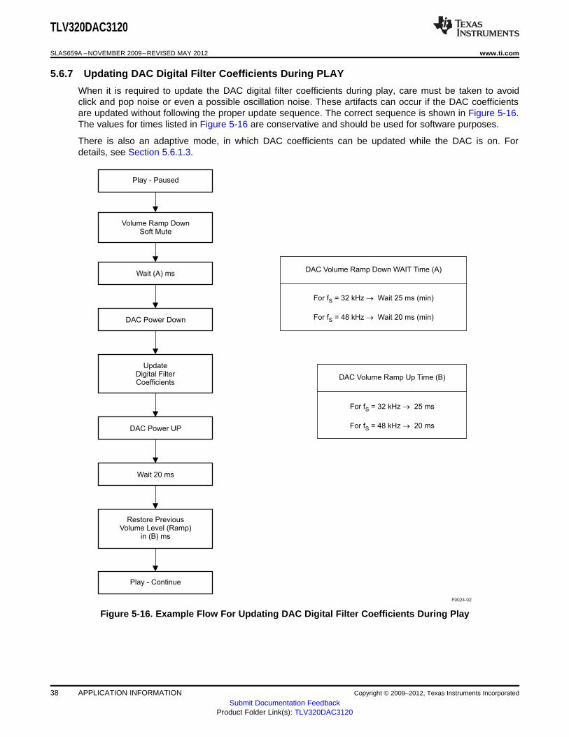
Play - Paused
DAC Power Down
UpdateDigital FilterCoefficients
DAC Power UP
Wait 20 ms
Volume Ramp DownSoft Mute
Restore PreviousVolume Level (Ramp)
in (B) ms
Play - Continue
Wait (A) ms
For f = 32 kHzS ® Wait 25 ms (min)
For f = 48 kHz Wait 20 ms (min)S ®
For = 32 kHz ®f 25 ms
For f = 48 kHz 20 ms
S
S ®
DAC Volume Ramp Down WAIT Time (A)
DAC Volume Ramp Up Time (B)
F0024-02
TLV320DAC3120
SLAS659A –NOVEMBER 2009–REVISED MAY 2012 www.ti.com
5.6.7 Updating DAC Digital Filter Coefficients During PLAY
When it is required to update the DAC digital filter coefficients during play, care must be taken to avoidclick and pop noise or even a possible oscillation noise. These artifacts can occur if the DAC coefficientsare updated without following the proper update sequence. The correct sequence is shown in Figure 5-16.The values for times listed in Figure 5-16 are conservative and should be used for software purposes.
There is also an adaptive mode, in which DAC coefficients can be updated while the DAC is on. Fordetails, see Section 5.6.1.3.
Figure 5-16. Example Flow For Updating DAC Digital Filter Coefficients During Play
38 APPLICATION INFORMATION Copyright © 2009–2012, Texas Instruments Incorporated
Submit Documentation FeedbackProduct Folder Link(s): TLV320DAC3120
TLV320DAC3120
www.ti.com SLAS659A –NOVEMBER 2009–REVISED MAY 2012
5.6.8 Digital Mixing and Routing
The TLV320DAC3120 has four digital mixing blocks. Each mixer can provide either mixing or multiplexingof the digital audio data. The first mixer/multiplexer can be used to select input data for the mono DACfrom left channel, right channel, or a mix of the left and right channels [(L + R) / 2]. This digital routing canbe configured by writing to page 0 / register 63, bits D5–D4 for the DAC mono channel.
5.6.9 Analog Audio Routing
The TLV320DAC3120 has the capability to route the DAC output to either the headphone or the speakeroutput. If desirable, both output drivers can be operated at the same time while playing at different volumelevels. The TLV320DAC3120 provides various digital routing capabilities, allowing digital mixing or evenchannel swapping in the digital domain. All analog outputs other than the selected ones can be powereddown for optimal power consumption.
5.6.9.1 Analog Output Volume Control
The output volume control can be used to fine-tune the level of the mixer amplifier signal supplied to theheadphone driver or the speaker driver. This architecture supports separate and concurrent volume levelsfor each of the four output drivers. This volume control can also be used as part of the output pop-noisereduction scheme. This feature is available even if the DAC is powered down.
5.6.9.2 Headphone Analog Output Volume Control
For the headphone outputs, the analog volume control has a range from 0 dB to –78 dB in 0.5-dB stepsfor most of the useful range plus mute, as shown in Table 5-19. This volume control includes soft-steppinglogic. Routing the DAC output signal to the analog volume control is done by writing to page 1 /register 35, bits D7–D6.
Changing the analog volume for the headphone is controlled by writing to page 1 / register 36,bits D6–D0. Routing the signal from the output of the analog volume control to the input of the headphonepower amplifier is done by writing to page 1 / register 36, bit D7.
The analog volume-control soft-stepping time is based on the setting in page 0 / register 63, bits D1–D0.
Copyright © 2009–2012, Texas Instruments Incorporated APPLICATION INFORMATION 39Submit Documentation Feedback
Product Folder Link(s): TLV320DAC3120
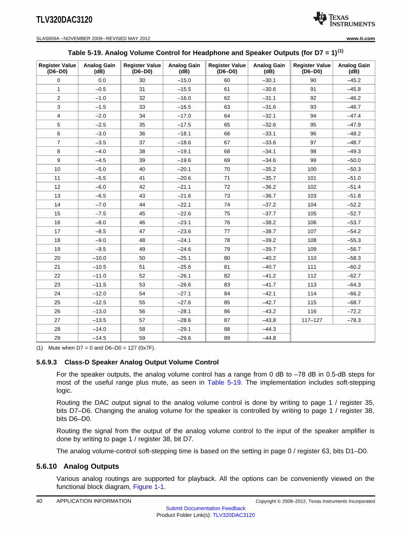
TLV320DAC3120
SLAS659A –NOVEMBER 2009–REVISED MAY 2012 www.ti.com
Table 5-19. Analog Volume Control for Headphone and Speaker Outputs (for D7 = 1) (1)
Register Value Analog Gain Register Value Analog Gain Register Value Analog Gain Register Value Analog Gain(D6–D0) (dB) (D6–D0) (dB) (D6–D0) (dB) (D6–D0) (dB)
0 0.0 30 –15.0 60 –30.1 90 –45.2
1 –0.5 31 –15.5 61 –30.6 91 –45.8
2 –1.0 32 –16.0 62 –31.1 92 –46.2
3 –1.5 33 –16.5 63 –31.6 93 –46.7
4 –2.0 34 –17.0 64 –32.1 94 –47.4
5 –2.5 35 –17.5 65 –32.6 95 –47.9
6 –3.0 36 –18.1 66 –33.1 96 –48.2
7 –3.5 37 –18.6 67 –33.6 97 –48.7
8 –4.0 38 –19.1 68 –34.1 98 –49.3
9 –4.5 39 –19.6 69 –34.6 99 –50.0
10 –5.0 40 –20.1 70 –35.2 100 –50.3
11 –5.5 41 –20.6 71 –35.7 101 –51.0
12 –6.0 42 –21.1 72 –36.2 102 –51.4
13 –6.5 43 –21.6 73 –36.7 103 –51.8
14 –7.0 44 –22.1 74 –37.2 104 –52.2
15 –7.5 45 –22.6 75 –37.7 105 –52.7
16 –8.0 46 –23.1 76 –38.2 106 –53.7
17 –8.5 47 –23.6 77 –38.7 107 –54.2
18 –9.0 48 –24.1 78 –39.2 108 –55.3
19 –9.5 49 –24.6 79 –39.7 109 –56.7
20 –10.0 50 –25.1 80 –40.2 110 –58.3
21 –10.5 51 –25.6 81 –40.7 111 –60.2
22 –11.0 52 –26.1 82 –41.2 112 –62.7
23 –11.5 53 –26.6 83 –41.7 113 –64.3
24 –12.0 54 –27.1 84 –42.1 114 –66.2
25 –12.5 55 –27.6 85 –42.7 115 –68.7
26 –13.0 56 –28.1 86 –43.2 116 –72.2
27 –13.5 57 –28.6 87 –43.8 117–127 –78.3
28 –14.0 58 –29.1 88 –44.3
29 –14.5 59 –29.6 89 –44.8
(1) Mute when D7 = 0 and D6–D0 = 127 (0x7F).
5.6.9.3 Class-D Speaker Analog Output Volume Control
For the speaker outputs, the analog volume control has a range from 0 dB to –78 dB in 0.5-dB steps formost of the useful range plus mute, as seen in Table 5-19. The implementation includes soft-steppinglogic.
Routing the DAC output signal to the analog volume control is done by writing to page 1 / register 35,bits D7–D6. Changing the analog volume for the speaker is controlled by writing to page 1 / register 38,bits D6–D0.
Routing the signal from the output of the analog volume control to the input of the speaker amplifier isdone by writing to page 1 / register 38, bit D7.
The analog volume-control soft-stepping time is based on the setting in page 0 / register 63, bits D1–D0.
5.6.10 Analog Outputs
Various analog routings are supported for playback. All the options can be conveniently viewed on thefunctional block diagram, Figure 1-1.
40 APPLICATION INFORMATION Copyright © 2009–2012, Texas Instruments Incorporated
Submit Documentation FeedbackProduct Folder Link(s): TLV320DAC3120
TLV320DAC3120
www.ti.com SLAS659A –NOVEMBER 2009–REVISED MAY 2012
5.6.10.1 Headphone Drivers
The TLV320DAC3120 features a mono headphone driver (HPOUT) that can deliver up to 30 mW perchannel, at 3.3-V supply voltage, into a 16-Ω load. The headphones are used in a single-endedconfiguration where an ac-coupling (dc-blocking) capacitor is connected between the device output pinsand the headphones. The headphone driver also supports 32-Ω and 10-kΩ loads without changing anycontrol register settings.
The headphone drivers can be configured to optimize the power consumption in the lineout-drive mode bywriting 11 to page 1 / register 44, bits D2–D1.
The output common mode of the headphone/lineout drivers can be programmed to 1.35 V, 1.5 V, 1.65 V,or 1.8 V by setting page 1 / register 31, bits D4–D3. The common-mode voltage should be set ≤ AVDD/2.
The headphone driver can be powered on by writing to page 1 / register 31, bit D7. The HPOUT outputdriver gain can be controlled by writing to page 1 / register 40, bits D6–D3, and it can be muted by writingto page 1 / register 40, bit D2.
The TLV320DAC3120 has a short-circuit protection feature for the headphone drivers, which is alwaysenabled to provide protection. The output condition of the headphone driver during short circuit can beprogrammed by writing to page 1 / register 31, bit D1. If D1 = 0 when a short circuit is detected, the devicelimits the maximum current to the load. If D1 = 1 when a short circuit is detected, the device powers downthe output driver. The default condition for headphones is the current-limiting mode. In case of a shortcircuit on either channel, the output is disabled and a status flag is provided as read-only bits on page 1 /register 31, bit D0. If shutdown mode is enabled, then as soon as the short circuit is detected, page 1 /register 31, bit D7 (for HPLOUT) clears automatically. Next, the device requires a reset to re-enable theoutput stage. Resetting can be done in two ways. First, the device master reset can be used, whichrequires either toggling the RESET pin or using the software reset. If master reset is used, it resets all ofthe registers. Second, a dedicated headphone power-stage reset can also be used to re-enable the outputstage, and that keeps all of the other device settings. The headphone power stage reset is done by settingpage 1 / register 31, bit D7 for HPLOUT. If the fault condition has been removed, then the device returnsto normal operation. If the fault is still present, then another shutdown occurs. Repeated resetting (morethan three times) is not recommended, as this could lead to overheating.
5.6.10.2 Speaker Drivers
The TLV320DAC3120 has an integrated class-D mono speaker driver (SPKP/SPKM) capable of driving an8-Ω or 4-Ω differential load. The speaker driver can be powered directly from the battery supply (2.7 V to5.5 V) on the SPKVDD pins; however, the voltage (including spike voltage) must be limited below theabsolute-maximum voltage of 6 V.
The speaker driver is capable of supplying 400 mW per channel with a 3.6-V power supply. Through theuse of digital mixing, the device can connect one or both digital audio playback data channels to eitherspeaker driver; this also allows digital channel swapping if needed.
The class-D speaker driver can be powered on by writing to page 1 / register 32, bit D7. The class-Doutput-driver gain can be controlled by writing to page 1 / register 42, bits D4–D3, and it can be muted bywriting to page 1 / register 42, bit D2.
The TLV320DAC3120 has a short-circuit protection feature for the speaker drivers that is always enabledto provide protection. If the output is shorted, the output stage shuts down on the overcurrent condition.(Current limiting is not an available option for the higher-current speaker driver output stage.) In case of ashort circuit, the output is disabled and a status flag is provided as a read-only bit on page 1 / register 32,bit D0.
Copyright © 2009–2012, Texas Instruments Incorporated APPLICATION INFORMATION 41Submit Documentation Feedback
Product Folder Link(s): TLV320DAC3120
TLV320DAC3120
SLAS659A –NOVEMBER 2009–REVISED MAY 2012 www.ti.com
If shutdown occurs due to an overcurrent condition, then the device requires a reset to re-enable theoutput stage. Resetting can be done in two ways. First, the device master reset can be used, whichrequires either toggling the RESET pin or using the software reset. If master reset is used, it resets all ofthe registers. Second, a dedicated speaker power-stage reset can be used that keeps all of the otherdevice settings. The speaker power-stage reset is done by setting page 1 / register 32, bit D7 for SPKPand SPKM. If the fault condition has been removed, then the device returns to normal operation. If thefault is still present, then another shutdown occurs. Repeated resetting (more than three times) is notrecommended, as this could lead to overheating.
To minimize battery current leakage, the SPKVDD voltage level should not be less than the AVDDvoltage level.
The TLV320DAC3120 has a thermal protection (OTP) feature for the speaker drivers which is alwaysenabled to provide protection. If the device is overheated, then the output stops switching. When thedevice cools down, the output resumes switching. An overtemperature status flag is provided as a read-only bit on page 0 / register 3, bit D1. The OTP feature is for self-protection of the device. If dietemperature can be controlled at the system/board level, then overtemperature does not occur.
5.6.11 Audio Output-Stage Power Configurations
After the device has been configured (following a RESET) and the circuitry has been powered up, theaudio output stage can be powered up and powered down by register control.
These functions soft-start automatically. By using these register controls, it is possible to turn all fourstages on at the same time without turning two of them off.
See Table 5-20 for register control of audio output stage power configurations.
Table 5-20. Audio Output Stage Power Configurations
Audio Output Pins Desired Function Page 1 / Register, Bit Value
HPOUT Power-down HPOUT driver Page 1 / register 31, bit D7 = 0
HPOUT Power-up HPOUT driver Page 1 / register 31, bit D7 = 1
SPKP / SPKM Power-down class-D driver Page 1 / register 32, bit D7 = 0
SPKP / SPKM Power-up class-D driver Page 1 / register 32, bit D7 = 1
5.7 CLOCK Generation and PLL
The TLV320DAC3120 supports a wide range of options for generating clocks for the DAC sections as wellas interface and other control blocks as shown in Figure 5-17. The clocks for the DAC require a sourcereference clock. This clock can be provided on a variety of device pins, such as the MCLK, BCLK, orGPIO1 pins. The source reference clock for the codec can be chosen by programming theCODEC_CLKIN value on page 0 / register 4, bits D1–D0. The CODEC_CLKIN can then be routed throughhighly-flexible clock dividers shown in Figure 5-17 to generate the various clocks required for the DAC andthe miniDSP section. In the event that the desired audio clocks cannot be generated from the referenceclocks on MCLK, BCLK, or GPIO1, the TLV320DAC3120 also provides the option of using the on-chipPLL which supports a wide range of fractional multiplication values to generate the required clocks.Starting from CODEC_CLKIN, the TLV320DAC3120 provides several programmable clock dividers to helpachieve a variety of sampling rates for the DAC and clocks for the miniDSP sections.
42 APPLICATION INFORMATION Copyright © 2009–2012, Texas Instruments Incorporated
Submit Documentation FeedbackProduct Folder Link(s): TLV320DAC3120
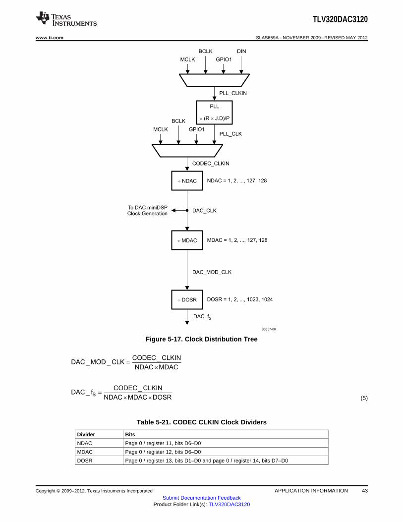
S
CODEC _ CLKINDAC _ f
NDAC MDAC DOSR=
´ ´
CODEC _ CLKINDAC _MOD _ CLK
NDAC MDAC=
´
PLL
´ ´(R J.D)/P
PLL_CLKIN
CODEC_CLKIN
DAC_MOD_CLK
DAC_CLK
NDAC = 1, 2, ..., 127, 128
MDAC = 1, 2, ..., 127, 128
DOSR = 1, 2, ..., 1023, 1024
MCLK
BCLK
GPIO1
DIN
MCLK
BCLK
GPIO1PLL_CLK
¸ MDAC
¸ DOSR
¸ NDAC
To DAC miniDSPClock Generation
DAC_fS
B0357-06
TLV320DAC3120
www.ti.com SLAS659A –NOVEMBER 2009–REVISED MAY 2012
Figure 5-17. Clock Distribution Tree
(5)
Table 5-21. CODEC CLKIN Clock Dividers
Divider Bits
NDAC Page 0 / register 11, bits D6–D0
MDAC Page 0 / register 12, bits D6–D0
DOSR Page 0 / register 13, bits D1–D0 and page 0 / register 14, bits D7–D0
Copyright © 2009–2012, Texas Instruments Incorporated APPLICATION INFORMATION 43Submit Documentation Feedback
Product Folder Link(s): TLV320DAC3120
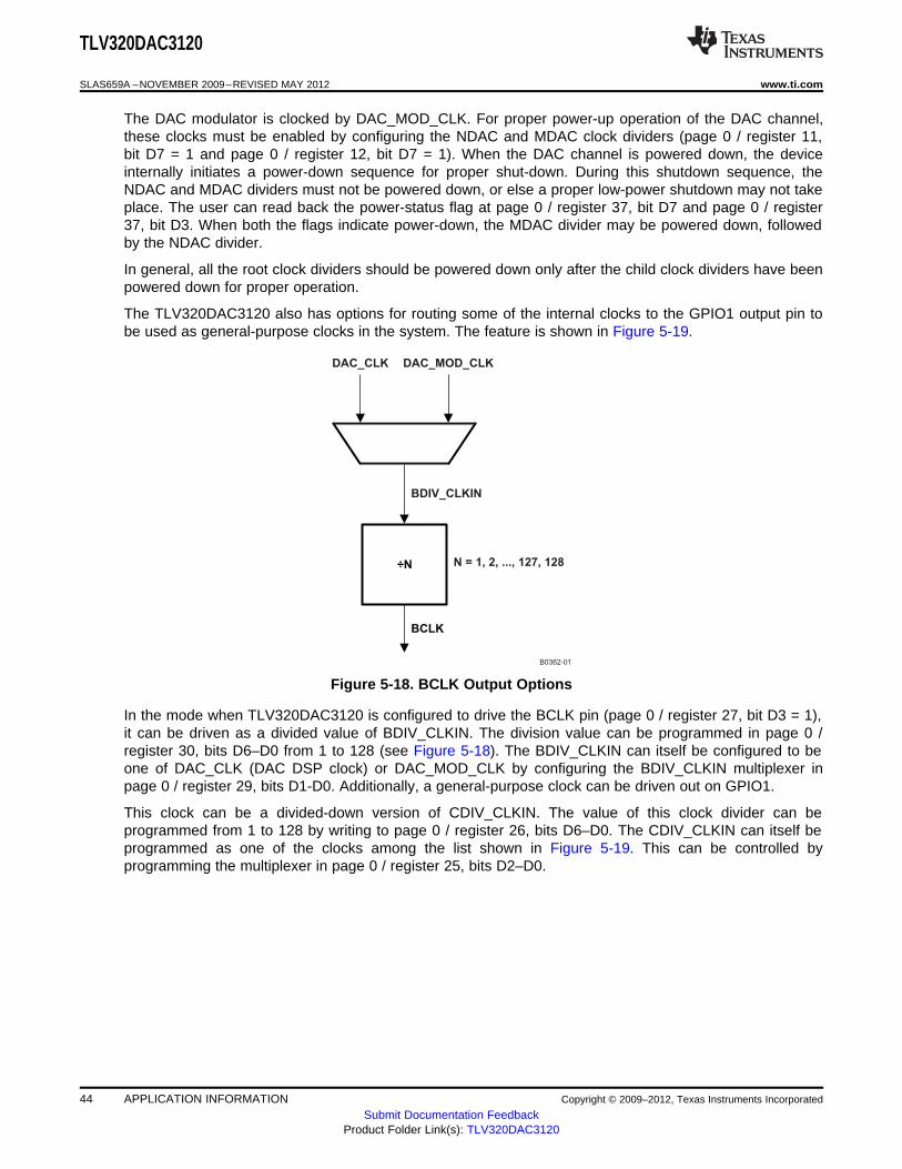
÷N
BCLK
DAC_CLK DAC_MOD_CLK
BDIV_CLKIN
N = 1, 2, ..., 127, 128
B0362-01
TLV320DAC3120
SLAS659A –NOVEMBER 2009–REVISED MAY 2012 www.ti.com
The DAC modulator is clocked by DAC_MOD_CLK. For proper power-up operation of the DAC channel,these clocks must be enabled by configuring the NDAC and MDAC clock dividers (page 0 / register 11,bit D7 = 1 and page 0 / register 12, bit D7 = 1). When the DAC channel is powered down, the deviceinternally initiates a power-down sequence for proper shut-down. During this shutdown sequence, theNDAC and MDAC dividers must not be powered down, or else a proper low-power shutdown may not takeplace. The user can read back the power-status flag at page 0 / register 37, bit D7 and page 0 / register37, bit D3. When both the flags indicate power-down, the MDAC divider may be powered down, followedby the NDAC divider.
In general, all the root clock dividers should be powered down only after the child clock dividers have beenpowered down for proper operation.
The TLV320DAC3120 also has options for routing some of the internal clocks to the GPIO1 output pin tobe used as general-purpose clocks in the system. The feature is shown in Figure 5-19.
Figure 5-18. BCLK Output Options
In the mode when TLV320DAC3120 is configured to drive the BCLK pin (page 0 / register 27, bit D3 = 1),it can be driven as a divided value of BDIV_CLKIN. The division value can be programmed in page 0 /register 30, bits D6–D0 from 1 to 128 (see Figure 5-18). The BDIV_CLKIN can itself be configured to beone of DAC_CLK (DAC DSP clock) or DAC_MOD_CLK by configuring the BDIV_CLKIN multiplexer inpage 0 / register 29, bits D1-D0. Additionally, a general-purpose clock can be driven out on GPIO1.
This clock can be a divided-down version of CDIV_CLKIN. The value of this clock divider can beprogrammed from 1 to 128 by writing to page 0 / register 26, bits D6–D0. The CDIV_CLKIN can itself beprogrammed as one of the clocks among the list shown in Figure 5-19. This can be controlled byprogramming the multiplexer in page 0 / register 25, bits D2–D0.
44 APPLICATION INFORMATION Copyright © 2009–2012, Texas Instruments Incorporated
Submit Documentation FeedbackProduct Folder Link(s): TLV320DAC3120
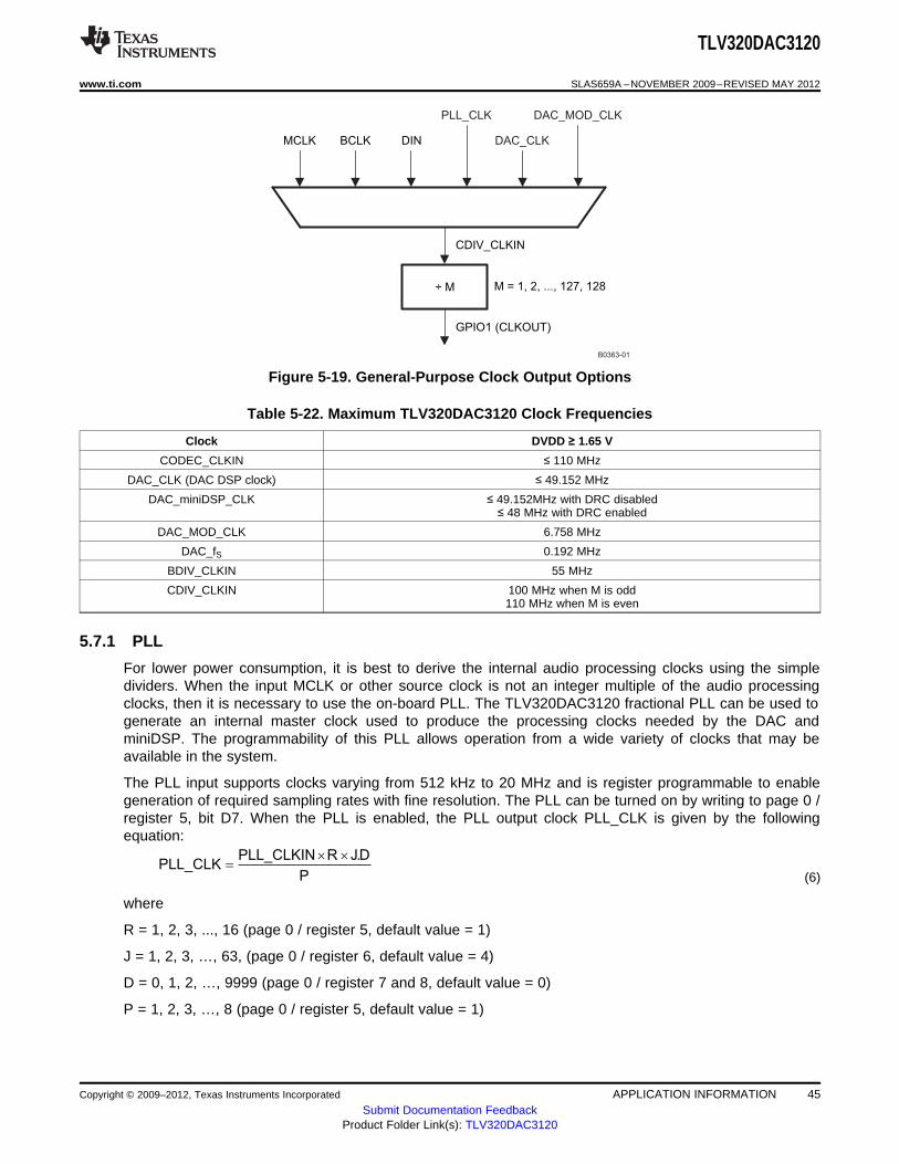
PLL_CLKIN R J.DPLL_CLK
P
´ ´
=
÷ M
GPIO1 (CLKOUT)
CDIV_CLKIN
MCLK BCLK DIN
PLL_CLK
DAC_CLK
DAC_MOD_CLK
M = 1, 2, ..., 127, 128
B0363-01
TLV320DAC3120
www.ti.com SLAS659A –NOVEMBER 2009–REVISED MAY 2012
Figure 5-19. General-Purpose Clock Output Options
Table 5-22. Maximum TLV320DAC3120 Clock Frequencies
Clock DVDD ≥ 1.65 V
CODEC_CLKIN ≤ 110 MHz
DAC_CLK (DAC DSP clock) ≤ 49.152 MHz
DAC_miniDSP_CLK ≤ 49.152MHz with DRC disabled≤ 48 MHz with DRC enabled
DAC_MOD_CLK 6.758 MHz
DAC_fS 0.192 MHz
BDIV_CLKIN 55 MHz
CDIV_CLKIN 100 MHz when M is odd110 MHz when M is even
5.7.1 PLL
For lower power consumption, it is best to derive the internal audio processing clocks using the simpledividers. When the input MCLK or other source clock is not an integer multiple of the audio processingclocks, then it is necessary to use the on-board PLL. The TLV320DAC3120 fractional PLL can be used togenerate an internal master clock used to produce the processing clocks needed by the DAC andminiDSP. The programmability of this PLL allows operation from a wide variety of clocks that may beavailable in the system.
The PLL input supports clocks varying from 512 kHz to 20 MHz and is register programmable to enablegeneration of required sampling rates with fine resolution. The PLL can be turned on by writing to page 0 /register 5, bit D7. When the PLL is enabled, the PLL output clock PLL_CLK is given by the followingequation:
(6)
where
R = 1, 2, 3, ..., 16 (page 0 / register 5, default value = 1)
J = 1, 2, 3, …, 63, (page 0 / register 6, default value = 4)
D = 0, 1, 2, …, 9999 (page 0 / register 7 and 8, default value = 0)
P = 1, 2, 3, …, 8 (page 0 / register 5, default value = 1)
Copyright © 2009–2012, Texas Instruments Incorporated APPLICATION INFORMATION 45Submit Documentation Feedback
Product Folder Link(s): TLV320DAC3120
PLL _ CLKIN10 MHz 20 MHz
P£ £
PLL _ CLKIN512 kHz 20 MHz
P£ £
TLV320DAC3120
SLAS659A –NOVEMBER 2009–REVISED MAY 2012 www.ti.com
The PLL can be turned on via page 0 / register 5, bit D7. The variable P can be programmed via page 0 /register 5, bits D6–D4. The variable R can be programmed via page 0 / register 5, bits D3–D0. Thevariable J can be programmed via page 0 / register 6, bits D5–D0. The variable D is 14 bits and isprogrammed into two registers. The MSB portion can be programmed via page 0 / register 7, bits D5–D0,and the LSB portion is programmed via page 0 / register 8, bits D7–D0. For proper update of the D-dividervalue, page 0 / register 7 must be programmed first, followed immediately by page 0 / register 8. Unlessthe write to page 0 / register 8 is completed, the new value of D does not take effect.
When the PLL is enabled, the following conditions must be satisfied.• When the PLL is enabled and D = 0, the following conditions must be satisfied for PLL_CLKIN:
(7)
80 MHz ≤ (PLL_CLKIN × J.D × R/P) ≤ 110 MHz (8)
4 ≤ R × J ≤ 259 (9)
• When the PLL is enabled and D ≠ 0, the following conditions must be satisfied for PLL_CLKIN:
(10)
80 MHz ≤ (PLL_CLKIN × J.D × R/P) ≤ 110 MHz (11)
R = 1 (12)
The PLL can be powered up independently from the DAC blocks, and can also be used as a general-purpose PLL by routing its output to the GPIO output. After powering up the PLL, PLL_CLK is availabletypically after 10 ms.
The clocks for codec and various signal processing blocks, CODEC_CLKIN can be generated from MCLKinput, BCLK input, GPIO input or PLL_CLK (page 0 / register 4, bit D1-D0).
If the CODEC_CLKIN is derived from the PLL, then the PLL must be powered up first and powered downlast.
Table 5-23 lists several example cases of typical PLL_CLKIN rates and how to program the PLL toachieve a sample rate fS of either 44.1 kHz or 48 kHz.
46 APPLICATION INFORMATION Copyright © 2009–2012, Texas Instruments Incorporated
Submit Documentation FeedbackProduct Folder Link(s): TLV320DAC3120
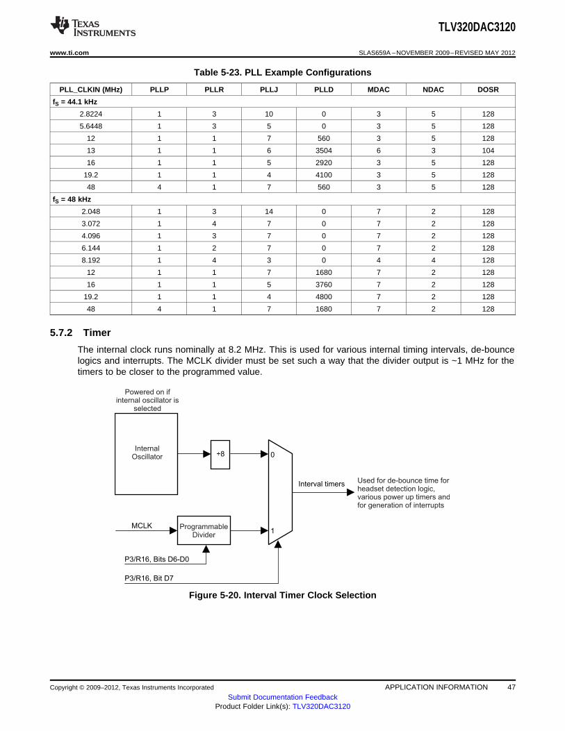
InternalOscillator ÷8 0
1
P3/R16, Bits D6-D0
MCLK
P3/R16, Bit D7
Interval timers
ProgrammableDivider
Powered on ifinternal oscillator is
selected
Used for de-bounce time forheadset detection logic,various power up timers andfor generation of interrupts
TLV320DAC3120
www.ti.com SLAS659A –NOVEMBER 2009–REVISED MAY 2012
Table 5-23. PLL Example Configurations
PLL_CLKIN (MHz) PLLP PLLR PLLJ PLLD MDAC NDAC DOSR
fS = 44.1 kHz
2.8224 1 3 10 0 3 5 128
5.6448 1 3 5 0 3 5 128
12 1 1 7 560 3 5 128
13 1 1 6 3504 6 3 104
16 1 1 5 2920 3 5 128
19.2 1 1 4 4100 3 5 128
48 4 1 7 560 3 5 128
fS = 48 kHz
2.048 1 3 14 0 7 2 128
3.072 1 4 7 0 7 2 128
4.096 1 3 7 0 7 2 128
6.144 1 2 7 0 7 2 128
8.192 1 4 3 0 4 4 128
12 1 1 7 1680 7 2 128
16 1 1 5 3760 7 2 128
19.2 1 1 4 4800 7 2 128
48 4 1 7 1680 7 2 128
5.7.2 Timer
The internal clock runs nominally at 8.2 MHz. This is used for various internal timing intervals, de-bouncelogics and interrupts. The MCLK divider must be set such a way that the divider output is ~1 MHz for thetimers to be closer to the programmed value.
Figure 5-20. Interval Timer Clock Selection
Copyright © 2009–2012, Texas Instruments Incorporated APPLICATION INFORMATION 47Submit Documentation Feedback
Product Folder Link(s): TLV320DAC3120
TLV320DAC3120
SLAS659A –NOVEMBER 2009–REVISED MAY 2012 www.ti.com
5.8 Digital Audio and Control Interface
5.8.1 Digital Audio Interface
Audio data is transferred between the host processor and the TLV320DAC3120 via the digital audio dataserial interface, or audio bus. The audio bus on this device is very flexible, including left- or right-justifieddata options, support for I2S or PCM protocols, programmable data-length options, a TDM mode formultichannel operation, very flexible master/slave configurability for each bus clock line, and the ability tocommunicate with multiple devices within a system directly.
NOTEThe TLV320AIC3102 has a mono DAC, which inputs the mono data from the digital audiodata serial interface as the left channel, the right channel, or a mix of the left and rightchannels as (L + R) ÷ 2 (page 0 / register 63, bits D5–D4). See Figure 1-1 for the signal flowof the DAC blocks.
The audio bus of the TLV320DAC3120 can be configured for left- or right-justified, I2S, DSP, or TDMmodes of operation, where communication with standard telephony PCM interfaces is supported within theTDM mode. These modes are all MSB-first, with data width programmable as 16, 20, 24, or 32 bits byconfiguring page 0 / register 27, bits D5–D4. In addition, the word clock and bit clock can beindependently configured in either master or slave mode for flexible connectivity to a wide variety ofprocessors. The word clock is used to define the beginning of a frame, and may be programmed as eithera pulse or a square-wave signal. The frequency of this clock corresponds to the maximum of the selectedDAC sampling frequencies.
The bit clock is used to clock in and clock out the digital audio data across the serial bus. When in mastermode, this signal can be programmed to generate variable clock pulses by controlling the bit-clock dividerin page 0 / register 30 (see Figure 5-17). The number of bit-clock pulses in a frame may need adjustmentto accommodate various word lengths as well as to support the case when multiple TLV320DAC3120smay share the same audio bus.
The TLV320DAC3120 also includes a feature to offset the position of start of data transfer with respect tothe word clock. This offset can be controlled in terms of number of bit clocks and can be programmed inpage 0 / register 28.
The TLV320DAC3120 also has the feature of inverting the polarity of the bit clock used for transferring theaudio data as compared to the default clock polarity used. This feature can be used independently of themode of audio interface chosen. This can be configured via page 0 / register 29, bit D3.
By default, when the word clocks and bit clocks are generated by the TLV320DAC3120, these clocks areactive only when the DAC is powered up within the device. This is done to save power. However, it alsosupports a feature when both the word clocks and bit clocks can be active even when the codec in thedevice is powered down. This is useful when using the TDM mode with multiple codecs on the same bus,or when word clocks or bit clocks are used in the system as general-purpose clocks.
5.8.1.1 Right-Justified Mode
The audio interface of the TLV320DAC3120 can be put into right-justified mode by programming page 0 /register 27, bits D7–D6 = 10. In right-justified mode, the LSB of the left channel is valid on the rising edgeof the bit clock preceding the falling edge of the word clock. Similarly, the LSB of the right channel is validon the rising edge of the bit clock preceding the rising edge of the word clock.
48 APPLICATION INFORMATION Copyright © 2009–2012, Texas Instruments Incorporated
Submit Documentation FeedbackProduct Folder Link(s): TLV320DAC3120
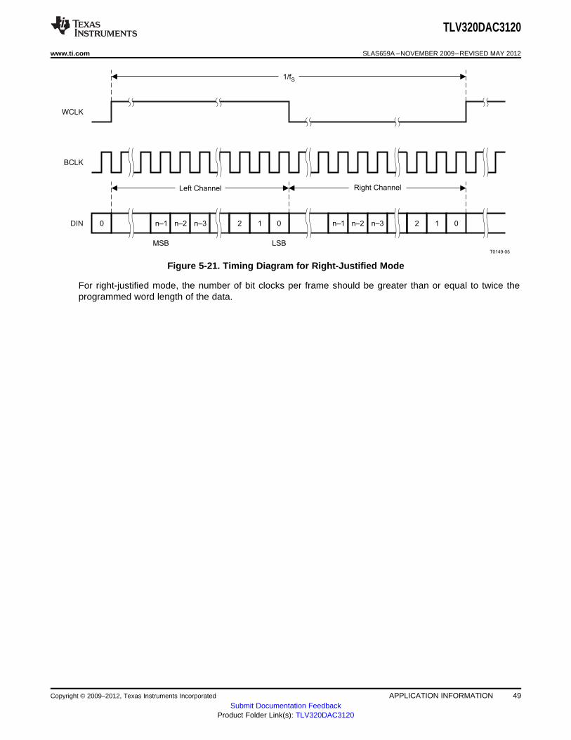
BCLK
WCLK
1 00 1 0
T0149-05
1/fS
LSBMSB
Left Channel Right Channel
2 2DIN n–1 n–1n–2 n–2n–3 n–3
TLV320DAC3120
www.ti.com SLAS659A –NOVEMBER 2009–REVISED MAY 2012
Figure 5-21. Timing Diagram for Right-Justified Mode
For right-justified mode, the number of bit clocks per frame should be greater than or equal to twice theprogrammed word length of the data.
Copyright © 2009–2012, Texas Instruments Incorporated APPLICATION INFORMATION 49Submit Documentation Feedback
Product Folder Link(s): TLV320DAC3120
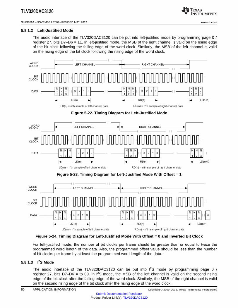
LD(n) LD(n+1)
WORDCLOCK
BITCLOCK
DATA 3N-1
N-2
N-3
2 1 03N-1
N-2
N-3
2 1 03N-1
N-2
N-3
RD(n)
LEFT CHANNEL RIGHT CHANNEL
LD(n) = n'th sample of left channel data RD(n) = n'th sample of right channel data
LD(n) LD(n+1)
WORDCLOCK
BITCLOCK
DATA -1
-2
-3
2 1 03 -1
-2
-3
2 1 03 -1
-2
N N N N N N N N N-3
RD(n)
LEFT CHANNEL RIGHT CHANNEL
LD(n) = n'th sample of left channel data RD(n) = n'th sample of right channel data
LD(n) LD(n+1)
WORDCLOCK
BITCLOCK
DATA -1
-2
-3
2 1 03 -1
-2
-3
2 1 03 -1
-2
N N N N N N N N N-3
RD(n)
LEFT CHANNEL RIGHT CHANNEL
LD(n) = n'th sample of left channel data RD(n) = n'th sample of right channel data
TLV320DAC3120
SLAS659A –NOVEMBER 2009–REVISED MAY 2012 www.ti.com
5.8.1.2 Left-Justified Mode
The audio interface of the TLV320DAC3120 can be put into left-justified mode by programming page 0 /register 27, bits D7–D6 = 11. In left-justified mode, the MSB of the right channel is valid on the rising edgeof the bit clock following the falling edge of the word clock. Similarly, the MSB of the left channel is validon the rising edge of the bit clock following the rising edge of the word clock.
Figure 5-22. Timing Diagram for Left-Justified Mode
Figure 5-23. Timing Diagram for Left-Justified Mode With Offset = 1
Figure 5-24. Timing Diagram for Left-Justified Mode With Offset = 0 and Inverted Bit Clock
For left-justified mode, the number of bit clocks per frame should be greater than or equal to twice theprogrammed word length of the data. Also, the programmed offset value should be less than the numberof bit clocks per frame by at least the programmed word length of the data.
5.8.1.3 I2S Mode
The audio interface of the TLV320DAC3120 can be put into I2S mode by programming page 0 /register 27, bits D7–D6 = to 00. In I2S mode, the MSB of the left channel is valid on the second risingedge of the bit clock after the falling edge of the word clock. Similarly, the MSB of the right channel is validon the second rising edge of the bit clock after the rising edge of the word clock.
50 APPLICATION INFORMATION Copyright © 2009–2012, Texas Instruments Incorporated
Submit Documentation FeedbackProduct Folder Link(s): TLV320DAC3120
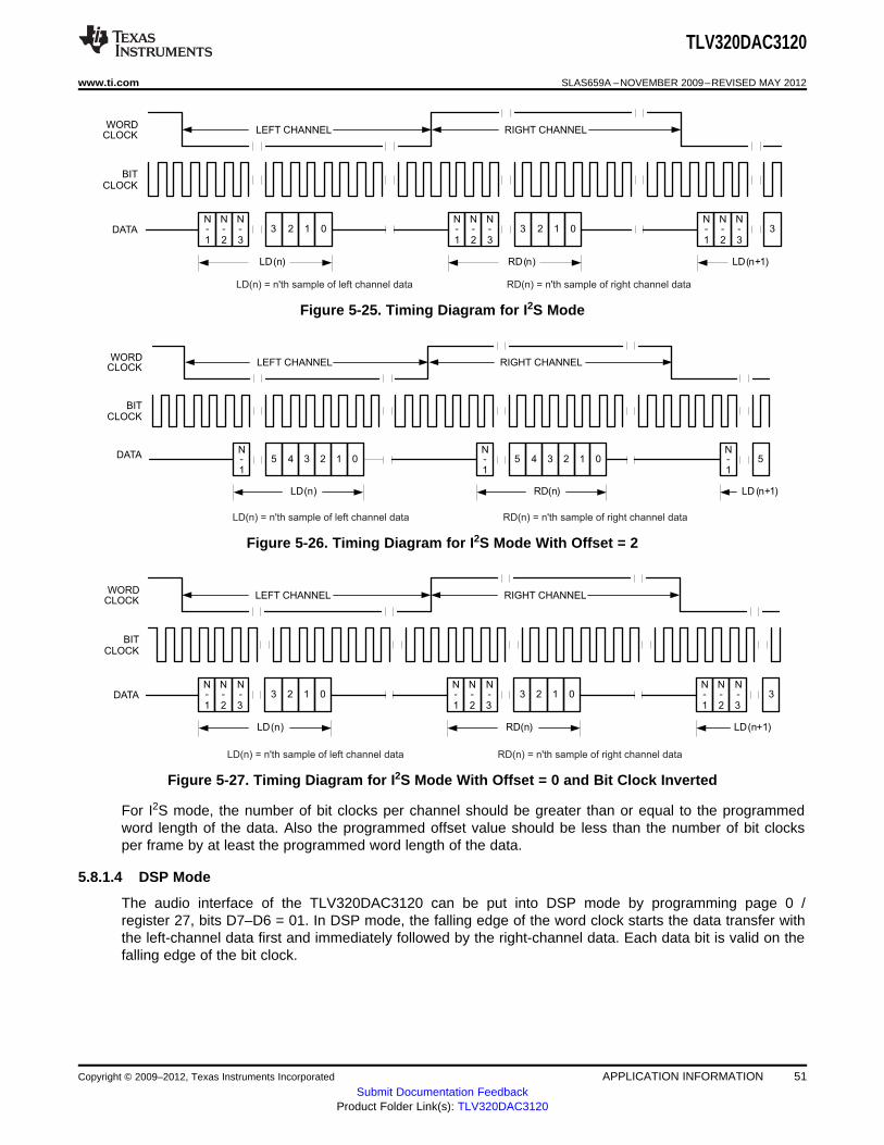
LD(n) LD(n+1)
WORDCLOCK
BITCLOCK
DATA -1
-2
-3
2 1 03 -1
-2
-3
2 1 03 -1
-2
N N N N N N N N N-3
3
RD(n)
LEFT CHANNEL RIGHT CHANNEL
LD(n) = n'th sample of left channel data RD(n) = n'th sample of right channel data
LD(n) LD (n+1)
WORDCLOCK
BITCLOCK
DATA -1
4 3 25 1 0 -1
4 3 25 1 0N N N
-1
5
RD(n)
LEFT CHANNEL RIGHT CHANNEL
LD(n) = n'th sample of left channel data RD(n) = n'th sample of right channel data
LD(n) LD(n+1)
WORDCLOCK
BITCLOCK
DATA -1
-2
-3
2 1 03 -1
-2
-3
2 1 03 -1
-2
N N N N N N N N N-3
3
RD(n)
LEFT CHANNEL RIGHT CHANNEL
LD(n) = n'th sample of left channel data RD(n) = n'th sample of right channel data
TLV320DAC3120
www.ti.com SLAS659A –NOVEMBER 2009–REVISED MAY 2012
Figure 5-25. Timing Diagram for I2S Mode
Figure 5-26. Timing Diagram for I2S Mode With Offset = 2
Figure 5-27. Timing Diagram for I2S Mode With Offset = 0 and Bit Clock Inverted
For I2S mode, the number of bit clocks per channel should be greater than or equal to the programmedword length of the data. Also the programmed offset value should be less than the number of bit clocksper frame by at least the programmed word length of the data.
5.8.1.4 DSP Mode
The audio interface of the TLV320DAC3120 can be put into DSP mode by programming page 0 /register 27, bits D7–D6 = 01. In DSP mode, the falling edge of the word clock starts the data transfer withthe left-channel data first and immediately followed by the right-channel data. Each data bit is valid on thefalling edge of the bit clock.
Copyright © 2009–2012, Texas Instruments Incorporated APPLICATION INFORMATION 51Submit Documentation Feedback
Product Folder Link(s): TLV320DAC3120
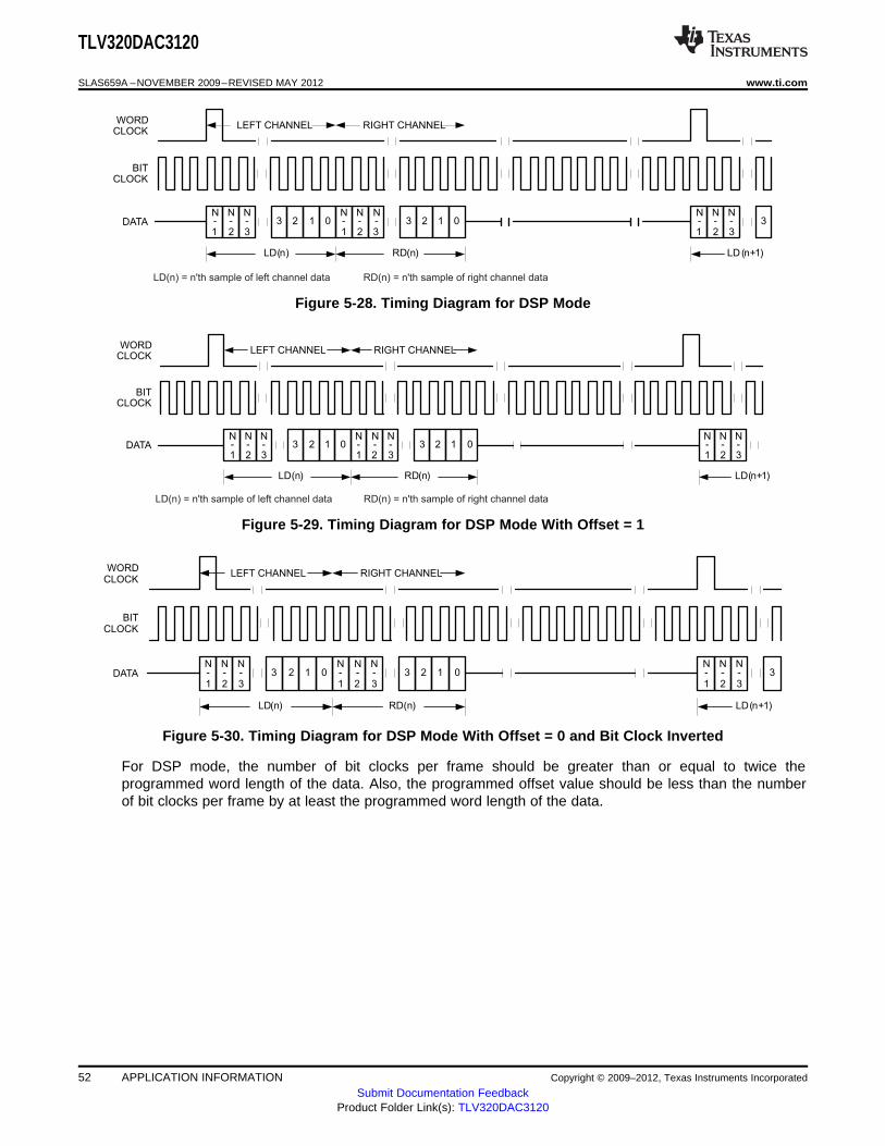
LD(n) LD(n+1)
BITCLOCK
DATAN-1
N-2
N-3
2 1 03N-1
N-2
N-3
03 2 1N-1
N-2
N-3
3
RD(n)
WORDCLOCK
LEFT CHANNEL RIGHT CHANNEL
LD(n) LD(n+1)
BITCLOCK
DATA -1
-2
-3
2 1 03 -1
-2
-3
03 2 1 -1
-2
N N N N N N N N N-3
RD(n)
WORDCLOCK
LEFT CHANNEL RIGHT CHANNEL
LD(n) = n'th sample of left channel data RD(n) = n'th sample of right channel data
LD(n) LD(n+1)
BITCLOCK
DATA -1
-2
-3
2 1 03 -1
-2
-3
03 2 1 -1
-2
N N N N N N N N N-3
3
RD(n)
WORDCLOCK
LEFT CHANNEL RIGHT CHANNEL
LD(n) = n'th sample of left channel data RD(n) = n'th sample of right channel data
TLV320DAC3120
SLAS659A –NOVEMBER 2009–REVISED MAY 2012 www.ti.com
Figure 5-28. Timing Diagram for DSP Mode
Figure 5-29. Timing Diagram for DSP Mode With Offset = 1
Figure 5-30. Timing Diagram for DSP Mode With Offset = 0 and Bit Clock Inverted
For DSP mode, the number of bit clocks per frame should be greater than or equal to twice theprogrammed word length of the data. Also, the programmed offset value should be less than the numberof bit clocks per frame by at least the programmed word length of the data.
52 APPLICATION INFORMATION Copyright © 2009–2012, Texas Instruments Incorporated
Submit Documentation FeedbackProduct Folder Link(s): TLV320DAC3120
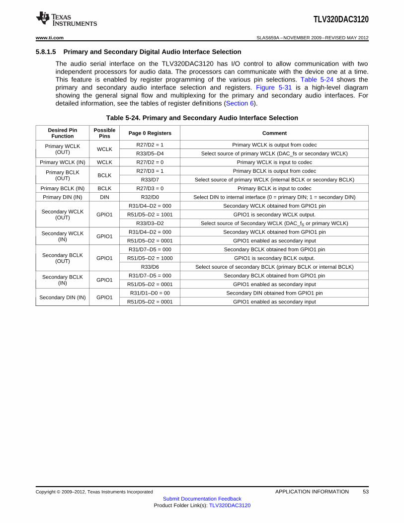
TLV320DAC3120
www.ti.com SLAS659A –NOVEMBER 2009–REVISED MAY 2012
5.8.1.5 Primary and Secondary Digital Audio Interface Selection
The audio serial interface on the TLV320DAC3120 has I/O control to allow communication with twoindependent processors for audio data. The processors can communicate with the device one at a time.This feature is enabled by register programming of the various pin selections. Table 5-24 shows theprimary and secondary audio interface selection and registers. Figure 5-31 is a high-level diagramshowing the general signal flow and multiplexing for the primary and secondary audio interfaces. Fordetailed information, see the tables of register definitions (Section 6).
Table 5-24. Primary and Secondary Audio Interface Selection
Desired Pin Possible Page 0 Registers CommentFunction Pins
R27/D2 = 1 Primary WCLK is output from codecPrimary WCLK WCLK(OUT) R33/D5–D4 Select source of primary WCLK (DAC_fs or secondary WCLK)
Primary WCLK (IN) WCLK R27/D2 = 0 Primary WCLK is input to codec
R27/D3 = 1 Primary BCLK is output from codecPrimary BCLK BCLK(OUT) R33/D7 Select source of primary WCLK (internal BCLK or secondary BCLK)
Primary BCLK (IN) BCLK R27/D3 = 0 Primary BCLK is input to codec
Primary DIN (IN) DIN R32/D0 Select DIN to internal interface (0 = primary DIN; 1 = secondary DIN)
R31/D4–D2 = 000 Secondary WCLK obtained from GPIO1 pinSecondary WCLK GPIO1 R51/D5–D2 = 1001 GPIO1 is secondary WCLK output.(OUT)
R33/D3–D2 Select source of Secondary WCLK (DAC_fS or primary WCLK)
R31/D4–D2 = 000 Secondary WCLK obtained from GPIO1 pinSecondary WCLK GPIO1(IN) R51/D5–D2 = 0001 GPIO1 enabled as secondary input
R31/D7–D5 = 000 Secondary BCLK obtained from GPIO1 pinSecondary BCLK GPIO1 R51/D5–D2 = 1000 GPIO1 is secondary BCLK output.(OUT)
R33/D6 Select source of secondary BCLK (primary BCLK or internal BCLK)
R31/D7–D5 = 000 Secondary BCLK obtained from GPIO1 pinSecondary BCLK GPIO1(IN) R51/D5–D2 = 0001 GPIO1 enabled as secondary input
R31/D1–D0 = 00 Secondary DIN obtained from GPIO1 pinSecondary DIN (IN) GPIO1
R51/D5–D2 = 0001 GPIO1 enabled as secondary input
Copyright © 2009–2012, Texas Instruments Incorporated APPLICATION INFORMATION 53Submit Documentation Feedback
Product Folder Link(s): TLV320DAC3120
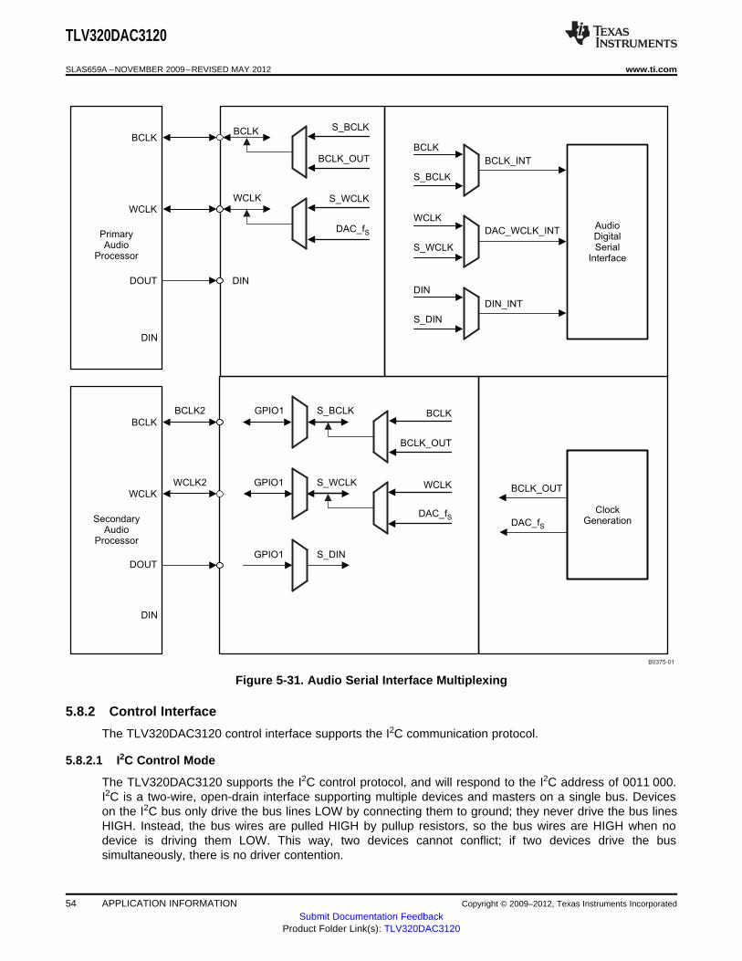
BCLK_OUT
DAC_fS
ClockGeneration
BCLK
S_BCLK
WCLK
S_WCLK
DIN
S_DIN
AudioDigitalSerial
Interface
BCLK_INT
DAC_WCLK_INT
DIN_INT
BCLK
WCLK
BCLK
DIN
WCLK
DIN
DOUT
PrimaryAudio
Processor
S_WCLK
S_BCLK
BCLK_OUT
GPIO1
GPIO1
S_BCLK BCLK
BCLK_OUT
S_WCLK WCLK
DAC_fS
DAC_fS
GPIO1 S_DIN
WCLK
DIN
DOUT
SecondaryAudio
Processor
BCLK
BCLK2
WCLK2
B0375-01
TLV320DAC3120
SLAS659A –NOVEMBER 2009–REVISED MAY 2012 www.ti.com
Figure 5-31. Audio Serial Interface Multiplexing
5.8.2 Control Interface
The TLV320DAC3120 control interface supports the I2C communication protocol.
5.8.2.1 I2C Control Mode
The TLV320DAC3120 supports the I2C control protocol, and will respond to the I2C address of 0011 000.I2C is a two-wire, open-drain interface supporting multiple devices and masters on a single bus. Deviceson the I2C bus only drive the bus lines LOW by connecting them to ground; they never drive the bus linesHIGH. Instead, the bus wires are pulled HIGH by pullup resistors, so the bus wires are HIGH when nodevice is driving them LOW. This way, two devices cannot conflict; if two devices drive the bussimultaneously, there is no driver contention.
54 APPLICATION INFORMATION Copyright © 2009–2012, Texas Instruments Incorporated
Submit Documentation FeedbackProduct Folder Link(s): TLV320DAC3120
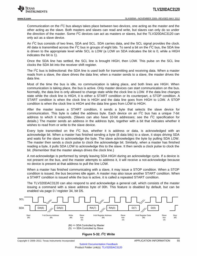
DA(6) DA(0) RA(7) RA(0) D(7) D(0)
Start
(M)
7-bit Device Address
(M)
Write
(M)
Slave
Ack
(S)
8-bit Register Address
(M)
Slave
Ack
(S)
8-bit Register Data
(M)
Stop
(M)
Slave
Ack
(S)
SDA
SCL
(M) => SDA Controlled by Master
(S) => SDA Controlled by Slave
TLV320DAC3120
www.ti.com SLAS659A –NOVEMBER 2009–REVISED MAY 2012
Communication on the I2C bus always takes place between two devices, one acting as the master and theother acting as the slave. Both masters and slaves can read and write, but slaves can only do so underthe direction of the master. Some I2C devices can act as masters or slaves, but the TLV320DAC3120 canonly act as a slave device.
An I2C bus consists of two lines, SDA and SCL. SDA carries data, and the SCL signal provides the clock.All data is transmitted across the I2C bus in groups of eight bits. To send a bit on the I2C bus, the SDA lineis driven to the appropriate level while SCL is LOW (a LOW on SDA indicates the bit is 0, while a HIGHindicates the bit is 1).
Once the SDA line has settled, the SCL line is brought HIGH, then LOW. This pulse on the SCL lineclocks the SDA bit into the receiver shift register.
The I2C bus is bidirectional: the SDA line is used both for transmitting and receiving data. When a masterreads from a slave, the slave drives the data line; when a master sends to a slave, the master drives thedata line.
Most of the time the bus is idle, no communication is taking place, and both lines are HIGH. Whencommunication is taking place, the bus is active. Only master devices can start communication on the bus.Normally, the data line is only allowed to change state while the clock line is LOW. If the data line changesstate while the clock line is HIGH, it is either a START condition or its counterpart, a STOP condition. ASTART condition is when the clock line is HIGH and the data line goes from HIGH to LOW. A STOPcondition is when the clock line is HIGH and the data line goes from LOW to HIGH.
After the master issues a START condition, it sends a byte that selects the slave device forcommunication. This byte is called the address byte. Each device on an I2C bus has a unique 7-bitaddress to which it responds. (Slaves can also have 10-bit addresses; see the I2C specification fordetails.) The master sends an address in the address byte, together with a bit that indicates whether itwishes to read from or write to the slave device.
Every byte transmitted on the I2C bus, whether it is address or data, is acknowledged with anacknowledge bit. When a master has finished sending a byte (8 data bits) to a slave, it stops driving SDAand waits for the slave to acknowledge the byte. The slave acknowledges the byte by pulling SDA LOW.The master then sends a clock pulse to clock the acknowledge bit. Similarly, when a master has finishedreading a byte, it pulls SDA LOW to acknowledge this to the slave. It then sends a clock pulse to clock thebit. (Remember that the master always drives the clock line.)
A not-acknowledge is performed by simply leaving SDA HIGH during an acknowledge cycle. If a device isnot present on the bus, and the master attempts to address it, it will receive a not-acknowledge becauseno device is present at that address to pull the line LOW.
When a master has finished communicating with a slave, it may issue a STOP condition. When a STOPcondition is issued, the bus becomes idle again. A master may also issue another START condition. Whena START condition is issued while the bus is active, it is called a repeated START condition.
The TLV320DAC3120 can also respond to and acknowledge a general call, which consists of the masterissuing a command with a slave address byte of 00h. This feature is disabled by default, but can beenabled via page 0 / register 34, bit D5.
Figure 5-32. I2C Write
Copyright © 2009–2012, Texas Instruments Incorporated APPLICATION INFORMATION 55Submit Documentation Feedback
Product Folder Link(s): TLV320DAC3120
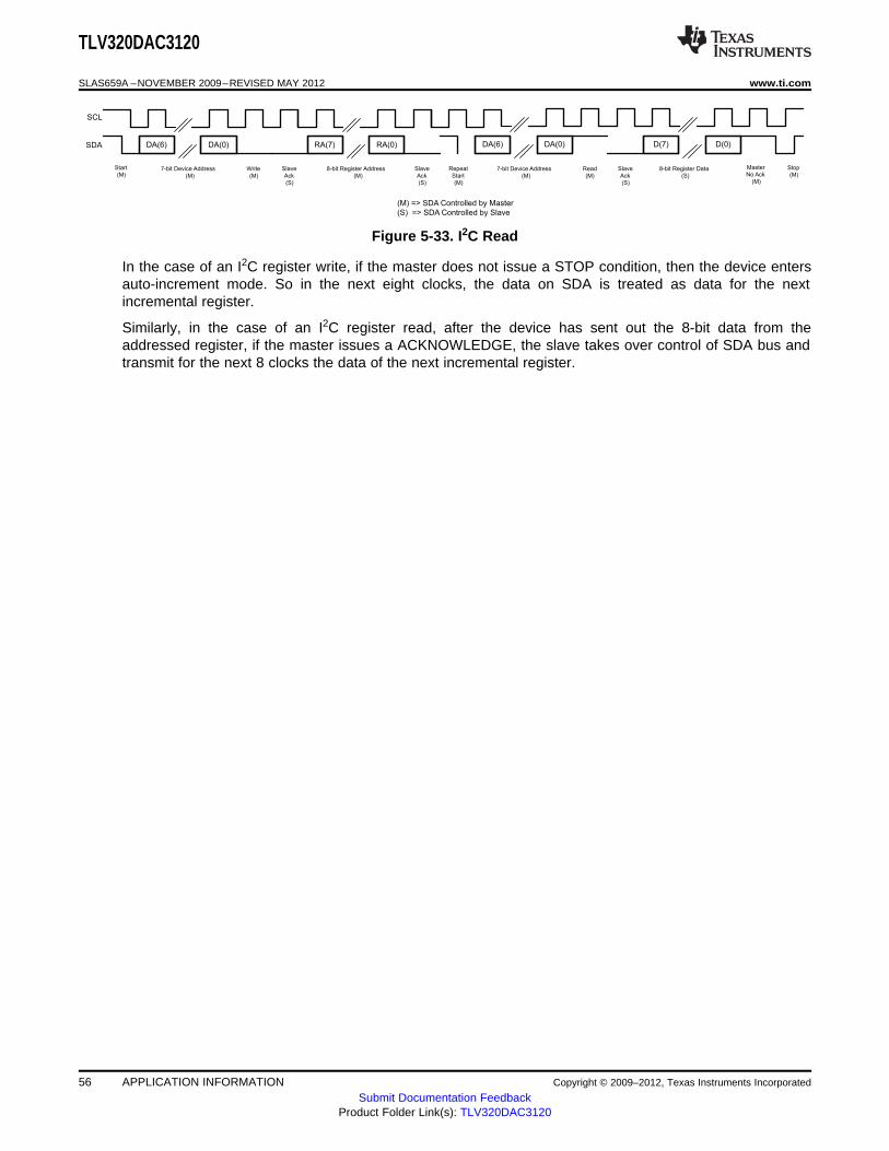
Start
(M)7-bit Device Address
(M)
Write
(M)
Slave
Ack
(S)
8-bit Register Address
(M)
Slave
Ack
(S)
SDA
SCL
7-bit Device Address
(M)
Read
(M)
Slave
Ack
(S)
DA(6) DA(0) RA(7) RA(0) DA(6) DA(0) D(7) D(0)
8-bit Register Data
(S)
Stop
(M)
Master
No Ack
(M)
Repeat
Start
(M)
(M) => SDA Controlled by Master
(S) => SDA Controlled by Slave
TLV320DAC3120
SLAS659A –NOVEMBER 2009–REVISED MAY 2012 www.ti.com
Figure 5-33. I2C Read
In the case of an I2C register write, if the master does not issue a STOP condition, then the device entersauto-increment mode. So in the next eight clocks, the data on SDA is treated as data for the nextincremental register.
Similarly, in the case of an I2C register read, after the device has sent out the 8-bit data from theaddressed register, if the master issues a ACKNOWLEDGE, the slave takes over control of SDA bus andtransmit for the next 8 clocks the data of the next incremental register.
56 APPLICATION INFORMATION Copyright © 2009–2012, Texas Instruments Incorporated
Submit Documentation FeedbackProduct Folder Link(s): TLV320DAC3120
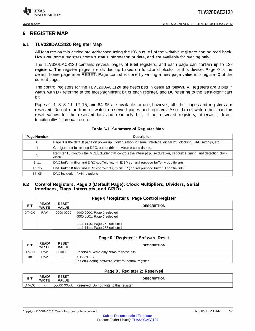
TLV320DAC3120
www.ti.com SLAS659A –NOVEMBER 2009–REVISED MAY 2012
6 REGISTER MAP
6.1 TLV320DAC3120 Register Map
All features on this device are addressed using the I2C bus. All of the writable registers can be read back.However, some registers contain status information or data, and are available for reading only.
The TLV320DAC3120 contains several pages of 8-bit registers, and each page can contain up to 128registers. The register pages are divided up based on functional blocks for this device. Page 0 is thedefault home page after RESET. Page control is done by writing a new page value into register 0 of thecurrent page.
The control registers for the TLV320DAC3120 are described in detail as follows. All registers are 8 bits inwidth, with D7 referring to the most-significant bit of each register, and D0 referring to the least-significantbit.
Pages 0, 1, 3, 8–11, 12–15, and 64–95 are available for use; however, all other pages and registers arereserved. Do not read from or write to reserved pages and registers. Also, do not write other than thereset values for the reserved bits and read-only bits of non-reserved registers; otherwise, devicefunctionality failure can occur.
Table 6-1. Summary of Register Map
Page Number Description
0 Page 0 is the default page on power up. Configuration for serial interface, digital I/O, clocking, DAC settings, etc.
1 Configuration for analog DAC, output drivers, volume controls, etc.
Register 16 controls the MCLK divider that controls the interrupt pulse duration, debounce timing, and detection block3 clock.
8–11 DAC buffer-A filter and DRC coefficients, miniDSP general-purpose buffer-A coefficients
12–15 DAC buffer-B filter and DRC coefficients, miniDSP general-purpose buffer B-coefficients
64–95 DAC instuction RAM locations
6.2 Control Registers, Page 0 (Default Page): Clock Multipliers, Dividers, SerialInterfaces, Flags, Interrupts, and GPIOs
Page 0 / Register 0: Page Control RegisterREAD/ RESETBIT DESCRIPTIONWRITE VALUE
D7–D0 R/W 0000 0000 0000 0000: Page 0 selected0000 0001: Page 1 selected...1111 1110: Page 254 selected1111 1111: Page 255 selected
Page 0 / Register 1: Software ResetREAD/ RESETBIT DESCRIPTIONWRITE VALUE
D7–D1 R/W 0000 000 Reserved. Write only zeros to these bits.
D0 R/W 0 0: Don't care1: Self-clearing software reset for control register
Page 0 / Register 2: ReservedREAD/ RESETBIT DESCRIPTIONWRITE VALUE
D7–D0 R XXXX XXXX Reserved. Do not write to this register.
Copyright © 2009–2012, Texas Instruments Incorporated REGISTER MAP 57Submit Documentation Feedback
Product Folder Link(s): TLV320DAC3120
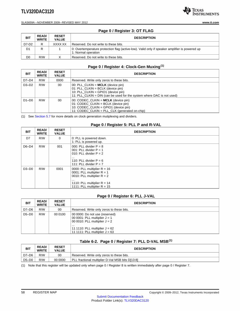
TLV320DAC3120
SLAS659A –NOVEMBER 2009–REVISED MAY 2012 www.ti.com
Page 0 / Register 3: OT FLAGREAD/ RESETBIT DESCRIPTIONWRITE VALUE
D7-D2 R XXXX XX Reserved. Do not write to these bits.
D1 R 1 0: Overtemperature protection flag (active-low). Valid only if speaker amplifier is powered up1: Normal operation
D0 R/W X Reserved. Do not write to these bits.
Page 0 / Register 4: Clock-Gen Muxing (1)
READ/ RESETBIT DESCRIPTIONWRITE VALUE
D7–D4 R/W 0000 Reserved. Write only zeros to these bits.
D3–D2 R/W 00 00: PLL_CLKIN = MCLK (device pin)01: PLL_CLKIN = BCLK (device pin)10: PLL_CLKIN = GPIO1 (device pin)11: PLL_CLKIN = DIN (can be used for the system where DAC is not used)
D1–D0 R/W 00 00: CODEC_CLKIN = MCLK (device pin)01: CODEC_CLKIN = BCLK (device pin)10: CODEC_CLKIN = GPIO1 (device pin)11: CODEC_CLKIN = PLL_CLK (generated on-chip)
(1) See Section 5.7 for more details on clock generation mutiplexing and dividers.
Page 0 / Register 5: PLL P and R-VALREAD/ RESETBIT DESCRIPTIONWRITE VALUE
D7 R/W 0 0: PLL is powered down.1: PLL is powered up.
D6–D4 R/W 001 000: PLL divider P = 8001: PLL divider P = 1010: PLL divider P = 2...110: PLL divider P = 6111: PLL divider P = 7
D3–D0 R/W 0001 0000: PLL multiplier R = 160001: PLL multiplier R = 10010: PLL multiplier R = 2...1110: PLL multiplier R = 141111: PLL multiplier R = 15
Page 0 / Register 6: PLL J-VALREAD/ RESETBIT DESCRIPTIONWRITE VALUE
D7–D6 R/W 00 Reserved. Write only zeros to these bits.
D5–D0 R/W 00 0100 00 0000: Do not use (reserved)00 0001: PLL multiplier J = 100 0010: PLL multiplier J = 2...11 1110: PLL multiplier J = 6211 1111: PLL multiplier J = 63
Table 6-2. Page 0 / Register 7: PLL D-VAL MSB (1)
READ/ RESETBIT DESCRIPTIONWRITE VALUE
D7–D6 R/W 00 Reserved. Write only zeros to these bits.
D5–D0 R/W 00 0000 PLL fractional multiplier D-Val MSB bits D[13:8]
(1) Note that this register will be updated only when page 0 / Register 8 is written immediately after page 0 / Register 7.
58 REGISTER MAP Copyright © 2009–2012, Texas Instruments Incorporated
Submit Documentation FeedbackProduct Folder Link(s): TLV320DAC3120
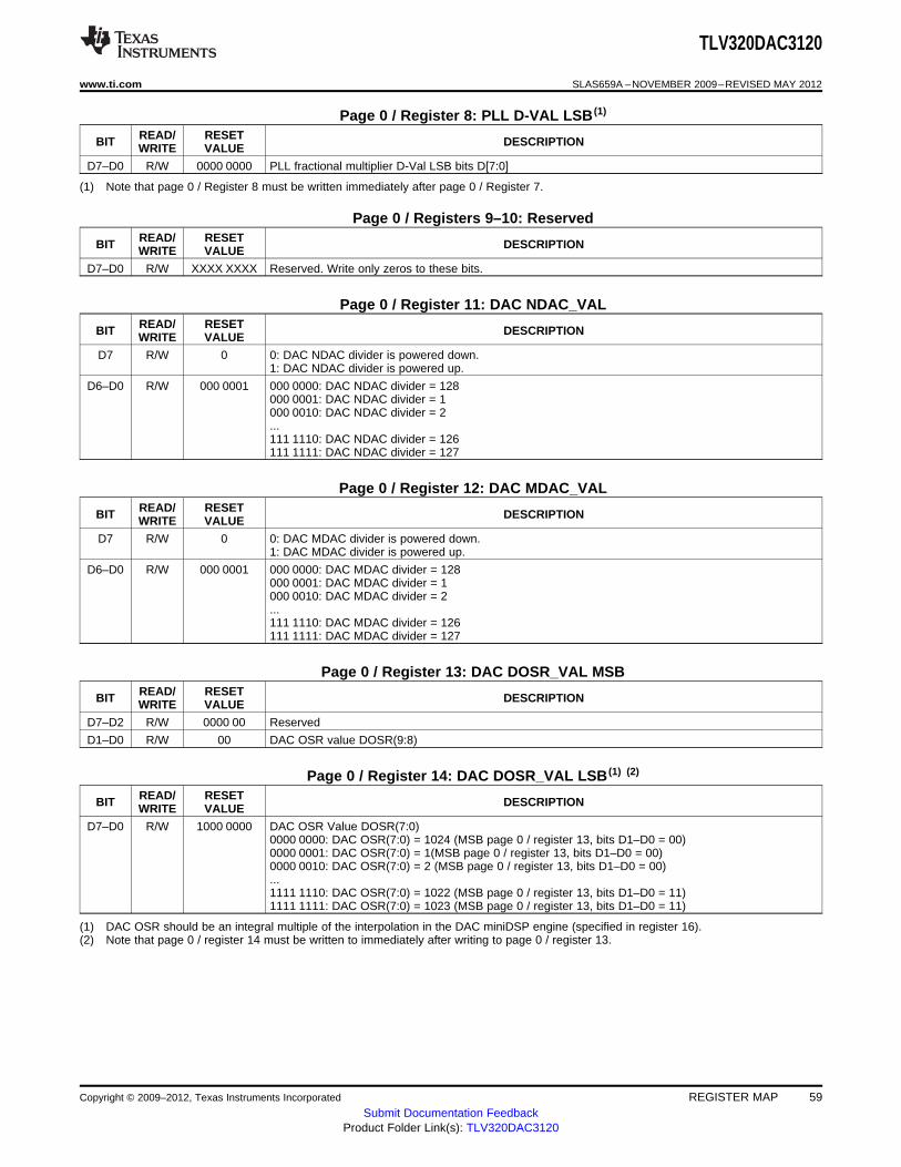
TLV320DAC3120
www.ti.com SLAS659A –NOVEMBER 2009–REVISED MAY 2012
Page 0 / Register 8: PLL D-VAL LSB (1)
READ/ RESETBIT DESCRIPTIONWRITE VALUE
D7–D0 R/W 0000 0000 PLL fractional multiplier D-Val LSB bits D[7:0]
(1) Note that page 0 / Register 8 must be written immediately after page 0 / Register 7.
Page 0 / Registers 9–10: ReservedREAD/ RESETBIT DESCRIPTIONWRITE VALUE
D7–D0 R/W XXXX XXXX Reserved. Write only zeros to these bits.
Page 0 / Register 11: DAC NDAC_VALREAD/ RESETBIT DESCRIPTIONWRITE VALUE
D7 R/W 0 0: DAC NDAC divider is powered down.1: DAC NDAC divider is powered up.
D6–D0 R/W 000 0001 000 0000: DAC NDAC divider = 128000 0001: DAC NDAC divider = 1000 0010: DAC NDAC divider = 2...111 1110: DAC NDAC divider = 126111 1111: DAC NDAC divider = 127
Page 0 / Register 12: DAC MDAC_VALREAD/ RESETBIT DESCRIPTIONWRITE VALUE
D7 R/W 0 0: DAC MDAC divider is powered down.1: DAC MDAC divider is powered up.
D6–D0 R/W 000 0001 000 0000: DAC MDAC divider = 128000 0001: DAC MDAC divider = 1000 0010: DAC MDAC divider = 2...111 1110: DAC MDAC divider = 126111 1111: DAC MDAC divider = 127
Page 0 / Register 13: DAC DOSR_VAL MSBREAD/ RESETBIT DESCRIPTIONWRITE VALUE
D7–D2 R/W 0000 00 Reserved
D1–D0 R/W 00 DAC OSR value DOSR(9:8)
Page 0 / Register 14: DAC DOSR_VAL LSB (1) (2)
READ/ RESETBIT DESCRIPTIONWRITE VALUE
D7–D0 R/W 1000 0000 DAC OSR Value DOSR(7:0)0000 0000: DAC OSR(7:0) = 1024 (MSB page 0 / register 13, bits D1–D0 = 00)0000 0001: DAC OSR(7:0) = 1(MSB page 0 / register 13, bits D1–D0 = 00)0000 0010: DAC OSR(7:0) = 2 (MSB page 0 / register 13, bits D1–D0 = 00)...1111 1110: DAC OSR(7:0) = 1022 (MSB page 0 / register 13, bits D1–D0 = 11)1111 1111: DAC OSR(7:0) = 1023 (MSB page 0 / register 13, bits D1–D0 = 11)
(1) DAC OSR should be an integral multiple of the interpolation in the DAC miniDSP engine (specified in register 16).(2) Note that page 0 / register 14 must be written to immediately after writing to page 0 / register 13.
Copyright © 2009–2012, Texas Instruments Incorporated REGISTER MAP 59Submit Documentation Feedback
Product Folder Link(s): TLV320DAC3120
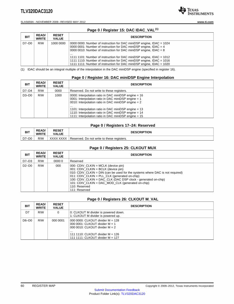
TLV320DAC3120
SLAS659A –NOVEMBER 2009–REVISED MAY 2012 www.ti.com
Page 0 / Register 15: DAC IDAC_VAL (1)
READ/ RESETBIT DESCRIPTIONWRITE VALUE
D7–D0 R/W 1000 0000 0000 0000: Number of instruction for DAC miniDSP engine, IDAC = 10240000 0001: Number of instruction for DAC miniDSP engine, IDAC = 40000 0010: Number of instruction for DAC miniDSP engine, IDAC = 8...1111 1101: Number of instruction for DAC miniDSP engine, IDAC = 10121111 1110: Number of instruction for DAC miniDSP engine, IDAC = 10161111 1111: Number of instruction for DAC miniDSP engine, IDAC = 1020
(1) IDAC should be an integral multiple of the interpolation in the DAC miniDSP engine (specified in register 16).
Page 0 / Register 16: DAC miniDSP Engine InterpolationREAD/ RESETBIT DESCRIPTIONWRITE VALUE
D7–D4 R/W 0000 Reserved. Do not write to these registers.
D3–D0 R/W 1000 0000: Interpolation ratio in DAC miniDSP engine = 160001: Interpolation ratio in DAC miniDSP engine = 10010: Interpolation ratio in DAC miniDSP engine = 2...1101: Interpolation ratio in DAC miniDSP engine = 131110: Interpolation ratio in DAC miniDSP engine = 141111: Interpolation ratio in DAC miniDSP engine = 15
Page 0 / Registers 17–24: ReservedREAD/ RESETBIT DESCRIPTIONWRITE VALUE
D7–D0 R/W XXXX XXXX Reserved. Do not write to these registers.
Page 0 / Registers 25: CLKOUT MUXREAD/ RESETBIT DESCRIPTIONWRITE VALUE
D7–D3 R/W 0000 0 Reserved
D2–D0 R/W 000 000: CDIV_CLKIN = MCLK (device pin)001: CDIV_CLKIN = BCLK (device pin)010: CDIV_CLKIN = DIN (can be used for the systems where DAC is not required)011: CDIV_CLKIN = PLL_CLK (generated on-chip)100: CDIV_CLKIN = DAC_CLK (DAC DSP clock - generated on-chip)101: CDIV_CLKIN = DAC_MOD_CLK (generated on-chip)110: Reserved111: Reserved
Page 0 / Registers 26: CLKOUT M_VALREAD/ RESETBIT DESCRIPTIONWRITE VALUE
D7 R/W 0 0: CLKOUT M divider is powered down.1: CLKOUT M divider is powered up.
D6–D0 R/W 000 0001 000 0000: CLKOUT divider M = 128000 0001: CLKOUT divider M = 1000 0010: CLKOUT divider M = 2...111 1110: CLKOUT divider M = 126111 1111: CLKOUT divider M = 127
60 REGISTER MAP Copyright © 2009–2012, Texas Instruments Incorporated
Submit Documentation FeedbackProduct Folder Link(s): TLV320DAC3120
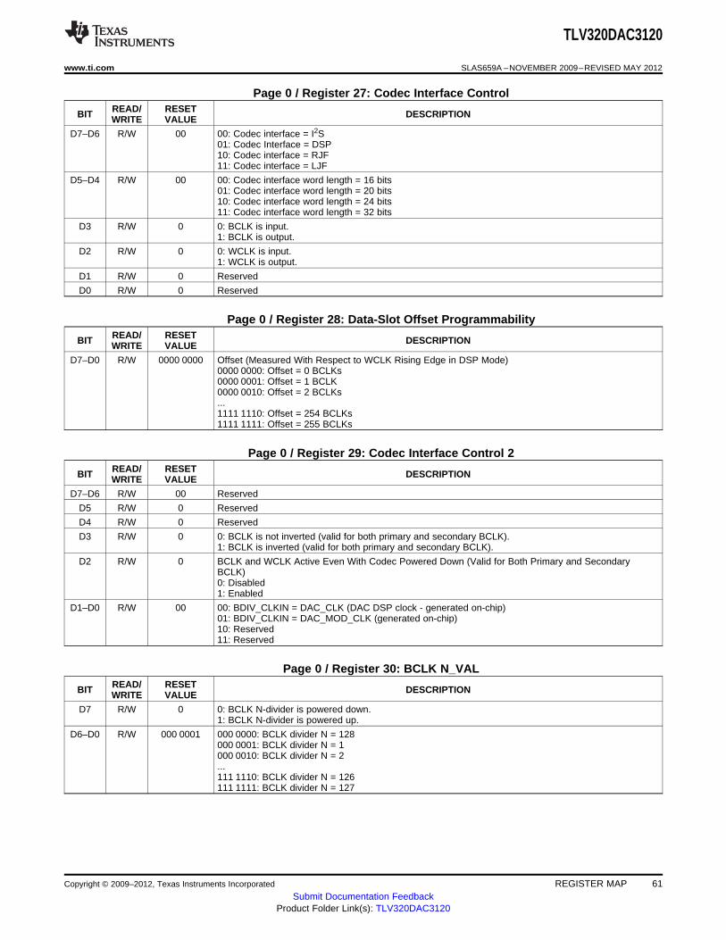
TLV320DAC3120
www.ti.com SLAS659A –NOVEMBER 2009–REVISED MAY 2012
Page 0 / Register 27: Codec Interface ControlREAD/ RESETBIT DESCRIPTIONWRITE VALUE
D7–D6 R/W 00 00: Codec interface = I2S01: Codec Interface = DSP10: Codec interface = RJF11: Codec interface = LJF
D5–D4 R/W 00 00: Codec interface word length = 16 bits01: Codec interface word length = 20 bits10: Codec interface word length = 24 bits11: Codec interface word length = 32 bits
D3 R/W 0 0: BCLK is input.1: BCLK is output.
D2 R/W 0 0: WCLK is input.1: WCLK is output.
D1 R/W 0 Reserved
D0 R/W 0 Reserved
Page 0 / Register 28: Data-Slot Offset ProgrammabilityREAD/ RESETBIT DESCRIPTIONWRITE VALUE
D7–D0 R/W 0000 0000 Offset (Measured With Respect to WCLK Rising Edge in DSP Mode)0000 0000: Offset = 0 BCLKs0000 0001: Offset = 1 BCLK0000 0010: Offset = 2 BCLKs...1111 1110: Offset = 254 BCLKs1111 1111: Offset = 255 BCLKs
Page 0 / Register 29: Codec Interface Control 2READ/ RESETBIT DESCRIPTIONWRITE VALUE
D7–D6 R/W 00 Reserved
D5 R/W 0 Reserved
D4 R/W 0 Reserved
D3 R/W 0 0: BCLK is not inverted (valid for both primary and secondary BCLK).1: BCLK is inverted (valid for both primary and secondary BCLK).
D2 R/W 0 BCLK and WCLK Active Even With Codec Powered Down (Valid for Both Primary and SecondaryBCLK)0: Disabled1: Enabled
D1–D0 R/W 00 00: BDIV_CLKIN = DAC_CLK (DAC DSP clock - generated on-chip)01: BDIV_CLKIN = DAC_MOD_CLK (generated on-chip)10: Reserved11: Reserved
Page 0 / Register 30: BCLK N_VALREAD/ RESETBIT DESCRIPTIONWRITE VALUE
D7 R/W 0 0: BCLK N-divider is powered down.1: BCLK N-divider is powered up.
D6–D0 R/W 000 0001 000 0000: BCLK divider N = 128000 0001: BCLK divider N = 1000 0010: BCLK divider N = 2...111 1110: BCLK divider N = 126111 1111: BCLK divider N = 127
Copyright © 2009–2012, Texas Instruments Incorporated REGISTER MAP 61Submit Documentation Feedback
Product Folder Link(s): TLV320DAC3120
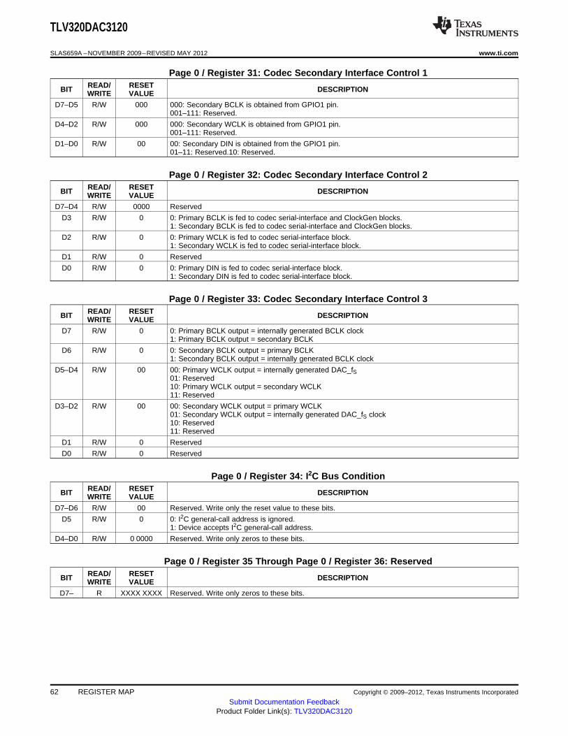
TLV320DAC3120
SLAS659A –NOVEMBER 2009–REVISED MAY 2012 www.ti.com
Page 0 / Register 31: Codec Secondary Interface Control 1READ/ RESETBIT DESCRIPTIONWRITE VALUE
D7–D5 R/W 000 000: Secondary BCLK is obtained from GPIO1 pin.001–111: Reserved.
D4–D2 R/W 000 000: Secondary WCLK is obtained from GPIO1 pin.001–111: Reserved.
D1–D0 R/W 00 00: Secondary DIN is obtained from the GPIO1 pin.01–11: Reserved.10: Reserved.
Page 0 / Register 32: Codec Secondary Interface Control 2READ/ RESETBIT DESCRIPTIONWRITE VALUE
D7–D4 R/W 0000 Reserved
D3 R/W 0 0: Primary BCLK is fed to codec serial-interface and ClockGen blocks.1: Secondary BCLK is fed to codec serial-interface and ClockGen blocks.
D2 R/W 0 0: Primary WCLK is fed to codec serial-interface block.1: Secondary WCLK is fed to codec serial-interface block.
D1 R/W 0 Reserved
D0 R/W 0 0: Primary DIN is fed to codec serial-interface block.1: Secondary DIN is fed to codec serial-interface block.
Page 0 / Register 33: Codec Secondary Interface Control 3READ/ RESETBIT DESCRIPTIONWRITE VALUE
D7 R/W 0 0: Primary BCLK output = internally generated BCLK clock1: Primary BCLK output = secondary BCLK
D6 R/W 0 0: Secondary BCLK output = primary BCLK1: Secondary BCLK output = internally generated BCLK clock
D5–D4 R/W 00 00: Primary WCLK output = internally generated DAC_fS01: Reserved10: Primary WCLK output = secondary WCLK11: Reserved
D3–D2 R/W 00 00: Secondary WCLK output = primary WCLK01: Secondary WCLK output = internally generated DAC_fS clock10: Reserved11: Reserved
D1 R/W 0 Reserved
D0 R/W 0 Reserved
Page 0 / Register 34: I2C Bus ConditionREAD/ RESETBIT DESCRIPTIONWRITE VALUE
D7–D6 R/W 00 Reserved. Write only the reset value to these bits.
D5 R/W 0 0: I2C general-call address is ignored.1: Device accepts I2C general-call address.
D4–D0 R/W 0 0000 Reserved. Write only zeros to these bits.
Page 0 / Register 35 Through Page 0 / Register 36: ReservedREAD/ RESETBIT DESCRIPTIONWRITE VALUE
D7– R XXXX XXXX Reserved. Write only zeros to these bits.
62 REGISTER MAP Copyright © 2009–2012, Texas Instruments Incorporated
Submit Documentation FeedbackProduct Folder Link(s): TLV320DAC3120
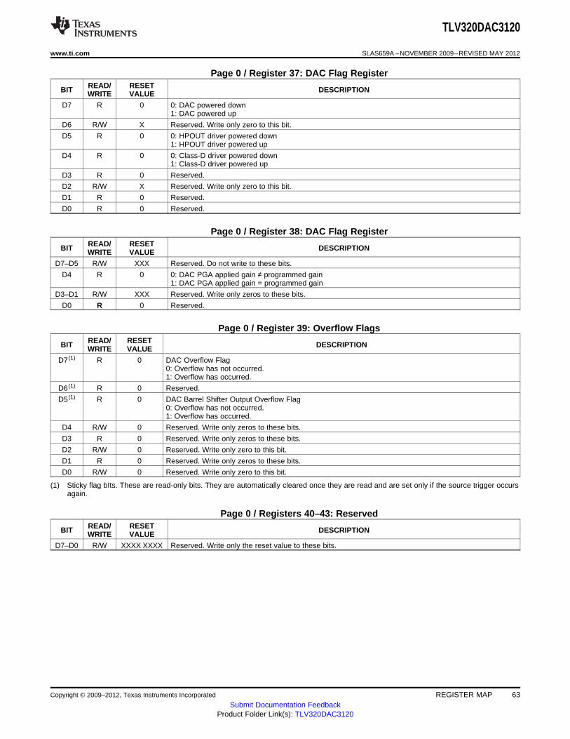
TLV320DAC3120
www.ti.com SLAS659A –NOVEMBER 2009–REVISED MAY 2012
Page 0 / Register 37: DAC Flag RegisterREAD/ RESETBIT DESCRIPTIONWRITE VALUE
D7 R 0 0: DAC powered down1: DAC powered up
D6 R/W X Reserved. Write only zero to this bit.
D5 R 0 0: HPOUT driver powered down1: HPOUT driver powered up
D4 R 0 0: Class-D driver powered down1: Class-D driver powered up
D3 R 0 Reserved.
D2 R/W X Reserved. Write only zero to this bit.
D1 R 0 Reserved.
D0 R 0 Reserved.
Page 0 / Register 38: DAC Flag RegisterREAD/ RESETBIT DESCRIPTIONWRITE VALUE
D7–D5 R/W XXX Reserved. Do not write to these bits.
D4 R 0 0: DAC PGA applied gain ≠ programmed gain1: DAC PGA applied gain = programmed gain
D3–D1 R/W XXX Reserved. Write only zeros to these bits.
D0 R 0 Reserved.
Page 0 / Register 39: Overflow FlagsREAD/ RESETBIT DESCRIPTIONWRITE VALUE
D7 (1) R 0 DAC Overflow Flag0: Overflow has not occurred.1: Overflow has occurred.
D6 (1) R 0 Reserved.
D5 (1) R 0 DAC Barrel Shifter Output Overflow Flag0: Overflow has not occurred.1: Overflow has occurred.
D4 R/W 0 Reserved. Write only zeros to these bits.
D3 R 0 Reserved. Write only zeros to these bits.
D2 R/W 0 Reserved. Write only zero to this bit.
D1 R 0 Reserved. Write only zeros to these bits.
D0 R/W 0 Reserved. Write only zero to this bit.
(1) Sticky flag bIts. These are read-only bits. They are automatically cleared once they are read and are set only if the source trigger occursagain.
Page 0 / Registers 40–43: ReservedREAD/ RESETBIT DESCRIPTIONWRITE VALUE
D7–D0 R/W XXXX XXXX Reserved. Write only the reset value to these bits.
Copyright © 2009–2012, Texas Instruments Incorporated REGISTER MAP 63Submit Documentation Feedback
Product Folder Link(s): TLV320DAC3120
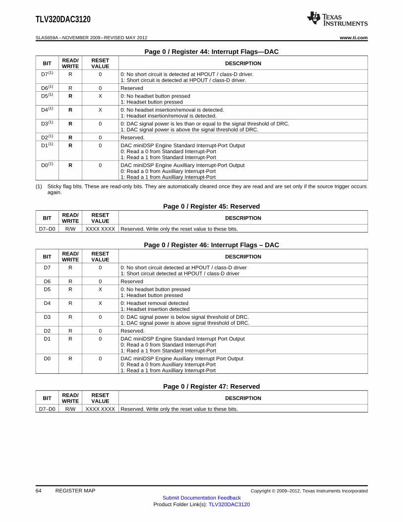
TLV320DAC3120
SLAS659A –NOVEMBER 2009–REVISED MAY 2012 www.ti.com
Page 0 / Register 44: Interrupt Flags—DACREAD/ RESETBIT DESCRIPTIONWRITE VALUE
D7 (1) R 0 0: No short circuit is detected at HPOUT / class-D driver.1: Short circuit is detected at HPOUT / class-D driver.
D6 (1) R 0 Reserved
D5 (1) R X 0: No headset button pressed1: Headset button pressed
D4 (1) R X 0: No headset insertion/removal is detected.1: Headset insertion/removal is detected.
D3 (1) R 0 0: DAC signal power is les than or equal to the signal threshold of DRC.1: DAC signal power is above the signal threshold of DRC.
D2 (1) R 0 Reserved.
D1 (1) R 0 DAC miniDSP Engine Standard Interrupt-Port Output0: Read a 0 from Standard Interrupt-Port1: Read a 1 from Standard Interrupt-Port
D0 (1) R 0 DAC miniDSP Engine Auxilliary Interrupt-Port Output0: Read a 0 from Auxilliary Interrupt-Port1: Read a 1 from Auxilliary Interrupt-Port
(1) Sticky flag bIts. These are read-only bits. They are automatically cleared once they are read and are set only if the source trigger occursagain.
Page 0 / Register 45: ReservedREAD/ RESETBIT DESCRIPTIONWRITE VALUE
D7–D0 R/W XXXX XXXX Reserved. Write only the reset value to these bits.
Page 0 / Register 46: Interrupt Flags – DACREAD/ RESETBIT DESCRIPTIONWRITE VALUE
D7 R 0 0: No short circuit detected at HPOUT / class-D driver1: Short circuit detected at HPOUT / class-D driver
D6 R 0 Reserved
D5 R X 0: No headset button pressed1: Headset button pressed
D4 R X 0: Headset removal detected1: Headset insertion detected
D3 R 0 0: DAC signal power is below signal threshold of DRC.1: DAC signal power is above signal threshold of DRC.
D2 R 0 Reserved.
D1 R 0 DAC miniDSP Engine Standard Interrupt Port Output0: Read a 0 from Standard Interrupt-Port1: Raed a 1 from Standard Interrupt-Port
D0 R 0 DAC miniDSP Engine Auxiliary Interrupt Port Output0: Read a 0 from Auxilliary Interrupt-Port1: Read a 1 from Auxilliary Interrupt-Port
Page 0 / Register 47: ReservedREAD/ RESETBIT DESCRIPTIONWRITE VALUE
D7–D0 R/W XXXX XXXX Reserved. Write only the reset value to these bits.
64 REGISTER MAP Copyright © 2009–2012, Texas Instruments Incorporated
Submit Documentation FeedbackProduct Folder Link(s): TLV320DAC3120
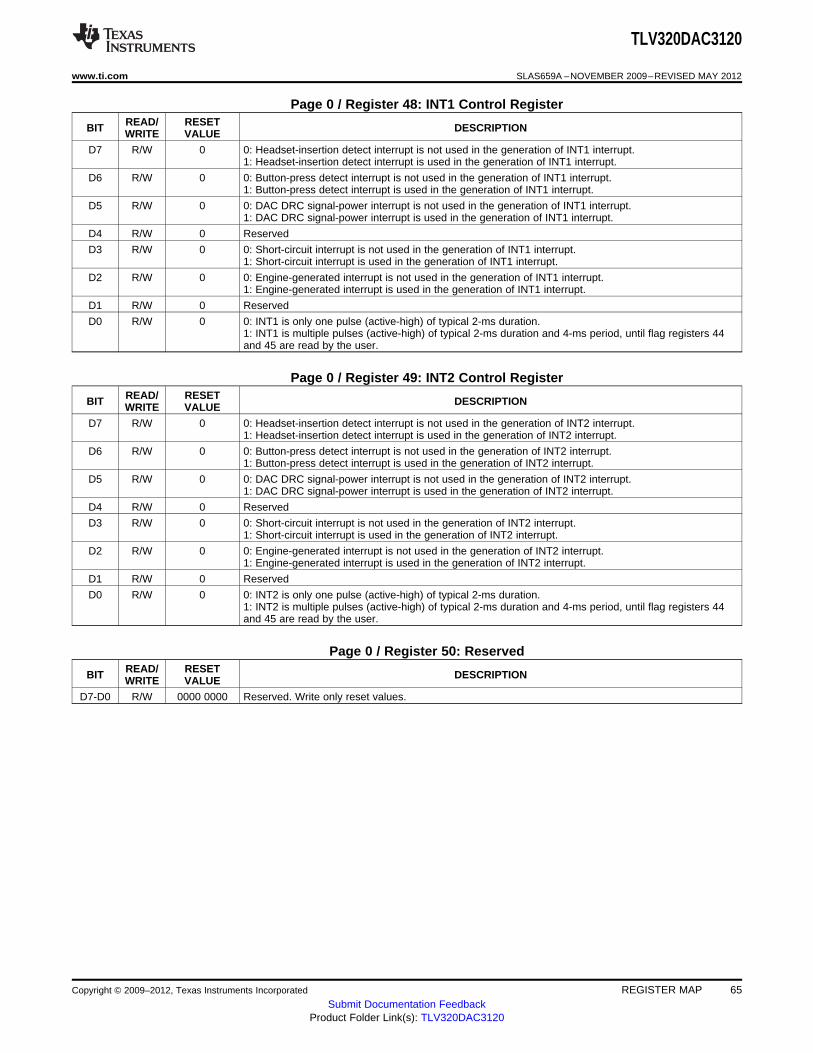
TLV320DAC3120
www.ti.com SLAS659A –NOVEMBER 2009–REVISED MAY 2012
Page 0 / Register 48: INT1 Control RegisterREAD/ RESETBIT DESCRIPTIONWRITE VALUE
D7 R/W 0 0: Headset-insertion detect interrupt is not used in the generation of INT1 interrupt.1: Headset-insertion detect interrupt is used in the generation of INT1 interrupt.
D6 R/W 0 0: Button-press detect interrupt is not used in the generation of INT1 interrupt.1: Button-press detect interrupt is used in the generation of INT1 interrupt.
D5 R/W 0 0: DAC DRC signal-power interrupt is not used in the generation of INT1 interrupt.1: DAC DRC signal-power interrupt is used in the generation of INT1 interrupt.
D4 R/W 0 Reserved
D3 R/W 0 0: Short-circuit interrupt is not used in the generation of INT1 interrupt.1: Short-circuit interrupt is used in the generation of INT1 interrupt.
D2 R/W 0 0: Engine-generated interrupt is not used in the generation of INT1 interrupt.1: Engine-generated interrupt is used in the generation of INT1 interrupt.
D1 R/W 0 Reserved
D0 R/W 0 0: INT1 is only one pulse (active-high) of typical 2-ms duration.1: INT1 is multiple pulses (active-high) of typical 2-ms duration and 4-ms period, until flag registers 44and 45 are read by the user.
Page 0 / Register 49: INT2 Control RegisterREAD/ RESETBIT DESCRIPTIONWRITE VALUE
D7 R/W 0 0: Headset-insertion detect interrupt is not used in the generation of INT2 interrupt.1: Headset-insertion detect interrupt is used in the generation of INT2 interrupt.
D6 R/W 0 0: Button-press detect interrupt is not used in the generation of INT2 interrupt.1: Button-press detect interrupt is used in the generation of INT2 interrupt.
D5 R/W 0 0: DAC DRC signal-power interrupt is not used in the generation of INT2 interrupt.1: DAC DRC signal-power interrupt is used in the generation of INT2 interrupt.
D4 R/W 0 Reserved
D3 R/W 0 0: Short-circuit interrupt is not used in the generation of INT2 interrupt.1: Short-circuit interrupt is used in the generation of INT2 interrupt.
D2 R/W 0 0: Engine-generated interrupt is not used in the generation of INT2 interrupt.1: Engine-generated interrupt is used in the generation of INT2 interrupt.
D1 R/W 0 Reserved
D0 R/W 0 0: INT2 is only one pulse (active-high) of typical 2-ms duration.1: INT2 is multiple pulses (active-high) of typical 2-ms duration and 4-ms period, until flag registers 44and 45 are read by the user.
Page 0 / Register 50: ReservedREAD/ RESETBIT DESCRIPTIONWRITE VALUE
D7-D0 R/W 0000 0000 Reserved. Write only reset values.
Copyright © 2009–2012, Texas Instruments Incorporated REGISTER MAP 65Submit Documentation Feedback
Product Folder Link(s): TLV320DAC3120
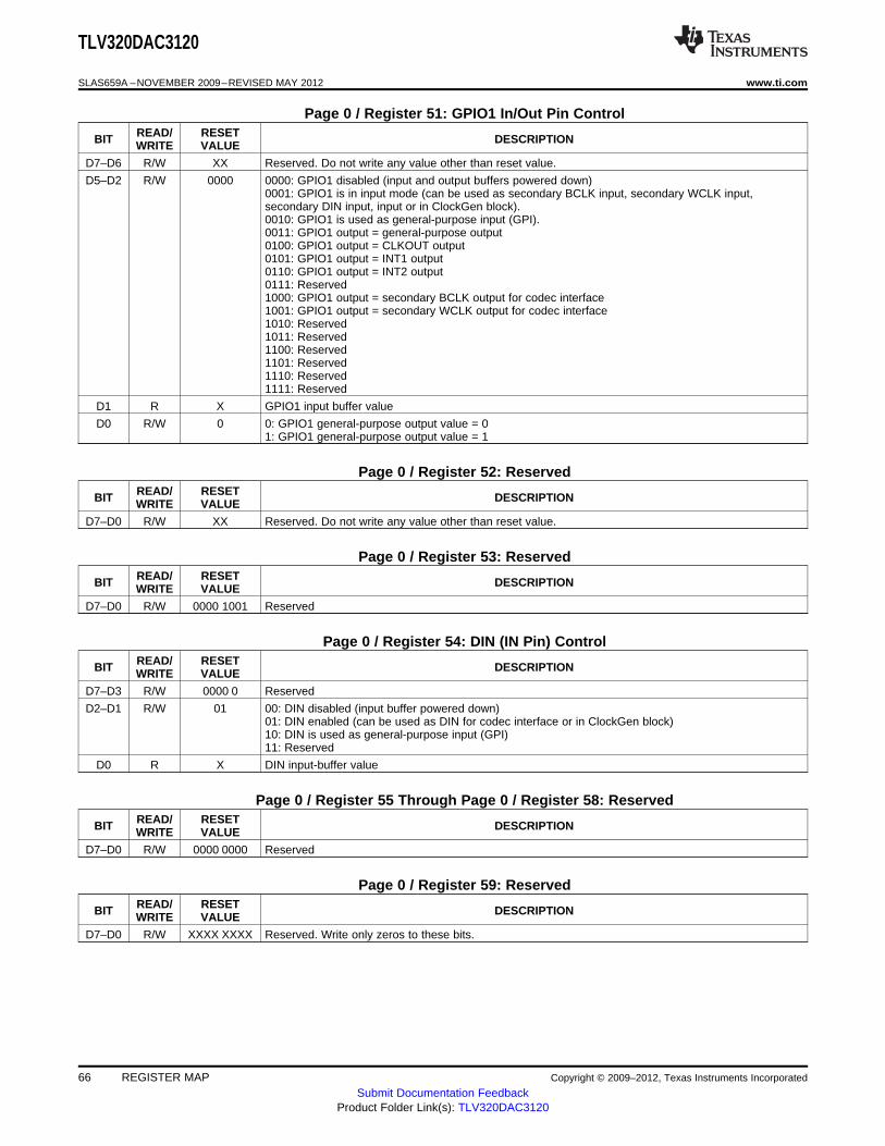
TLV320DAC3120
SLAS659A –NOVEMBER 2009–REVISED MAY 2012 www.ti.com
Page 0 / Register 51: GPIO1 In/Out Pin ControlREAD/ RESETBIT DESCRIPTIONWRITE VALUE
D7–D6 R/W XX Reserved. Do not write any value other than reset value.
D5–D2 R/W 0000 0000: GPIO1 disabled (input and output buffers powered down)0001: GPIO1 is in input mode (can be used as secondary BCLK input, secondary WCLK input,secondary DIN input, input or in ClockGen block).0010: GPIO1 is used as general-purpose input (GPI).0011: GPIO1 output = general-purpose output0100: GPIO1 output = CLKOUT output0101: GPIO1 output = INT1 output0110: GPIO1 output = INT2 output0111: Reserved1000: GPIO1 output = secondary BCLK output for codec interface1001: GPIO1 output = secondary WCLK output for codec interface1010: Reserved1011: Reserved1100: Reserved1101: Reserved1110: Reserved1111: Reserved
D1 R X GPIO1 input buffer value
D0 R/W 0 0: GPIO1 general-purpose output value = 01: GPIO1 general-purpose output value = 1
Page 0 / Register 52: ReservedREAD/ RESETBIT DESCRIPTIONWRITE VALUE
D7–D0 R/W XX Reserved. Do not write any value other than reset value.
Page 0 / Register 53: ReservedREAD/ RESETBIT DESCRIPTIONWRITE VALUE
D7–D0 R/W 0000 1001 Reserved
Page 0 / Register 54: DIN (IN Pin) ControlREAD/ RESETBIT DESCRIPTIONWRITE VALUE
D7–D3 R/W 0000 0 Reserved
D2–D1 R/W 01 00: DIN disabled (input buffer powered down)01: DIN enabled (can be used as DIN for codec interface or in ClockGen block)10: DIN is used as general-purpose input (GPI)11: Reserved
D0 R X DIN input-buffer value
Page 0 / Register 55 Through Page 0 / Register 58: ReservedREAD/ RESETBIT DESCRIPTIONWRITE VALUE
D7–D0 R/W 0000 0000 Reserved
Page 0 / Register 59: ReservedREAD/ RESETBIT DESCRIPTIONWRITE VALUE
D7–D0 R/W XXXX XXXX Reserved. Write only zeros to these bits.
66 REGISTER MAP Copyright © 2009–2012, Texas Instruments Incorporated
Submit Documentation FeedbackProduct Folder Link(s): TLV320DAC3120
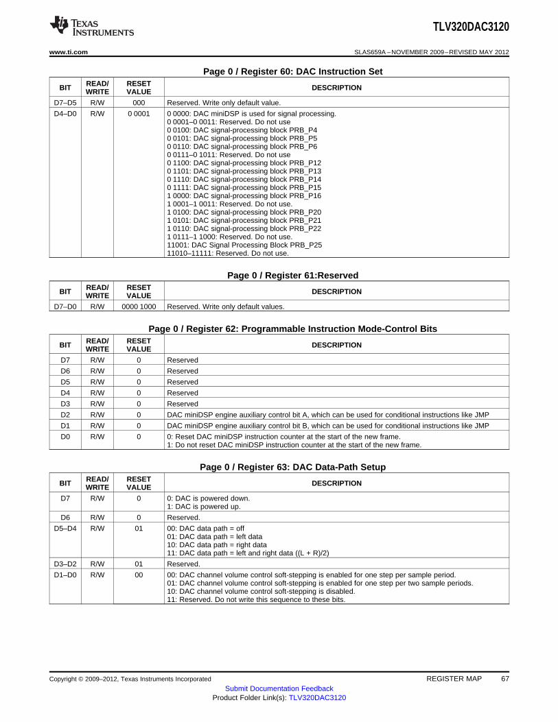
TLV320DAC3120
www.ti.com SLAS659A –NOVEMBER 2009–REVISED MAY 2012
Page 0 / Register 60: DAC Instruction SetREAD/ RESETBIT DESCRIPTIONWRITE VALUE
D7–D5 R/W 000 Reserved. Write only default value.
D4–D0 R/W 0 0001 0 0000: DAC miniDSP is used for signal processing.0 0001–0 0011: Reserved. Do not use0 0100: DAC signal-processing block PRB_P40 0101: DAC signal-processing block PRB_P50 0110: DAC signal-processing block PRB_P60 0111–0 1011: Reserved. Do not use0 1100: DAC signal-processing block PRB_P120 1101: DAC signal-processing block PRB_P130 1110: DAC signal-processing block PRB_P140 1111: DAC signal-processing block PRB_P151 0000: DAC signal-processing block PRB_P161 0001–1 0011: Reserved. Do not use.1 0100: DAC signal-processing block PRB_P201 0101: DAC signal-processing block PRB_P211 0110: DAC signal-processing block PRB_P221 0111–1 1000: Reserved. Do not use.11001: DAC Signal Processing Block PRB_P2511010–11111: Reserved. Do not use.
Page 0 / Register 61:ReservedREAD/ RESETBIT DESCRIPTIONWRITE VALUE
D7–D0 R/W 0000 1000 Reserved. Write only default values.
Page 0 / Register 62: Programmable Instruction Mode-Control BitsREAD/ RESETBIT DESCRIPTIONWRITE VALUE
D7 R/W 0 Reserved
D6 R/W 0 Reserved
D5 R/W 0 Reserved
D4 R/W 0 Reserved
D3 R/W 0 Reserved
D2 R/W 0 DAC miniDSP engine auxiliary control bit A, which can be used for conditional instructions like JMP
D1 R/W 0 DAC miniDSP engine auxiliary control bit B, which can be used for conditional instructions like JMP
D0 R/W 0 0: Reset DAC miniDSP instruction counter at the start of the new frame.1: Do not reset DAC miniDSP instruction counter at the start of the new frame.
Page 0 / Register 63: DAC Data-Path SetupREAD/ RESETBIT DESCRIPTIONWRITE VALUE
D7 R/W 0 0: DAC is powered down.1: DAC is powered up.
D6 R/W 0 Reserved.
D5–D4 R/W 01 00: DAC data path = off01: DAC data path = left data10: DAC data path = right data11: DAC data path = left and right data ((L + R)/2)
D3–D2 R/W 01 Reserved.
D1–D0 R/W 00 00: DAC channel volume control soft-stepping is enabled for one step per sample period.01: DAC channel volume control soft-stepping is enabled for one step per two sample periods.10: DAC channel volume control soft-stepping is disabled.11: Reserved. Do not write this sequence to these bits.
Copyright © 2009–2012, Texas Instruments Incorporated REGISTER MAP 67Submit Documentation Feedback
Product Folder Link(s): TLV320DAC3120
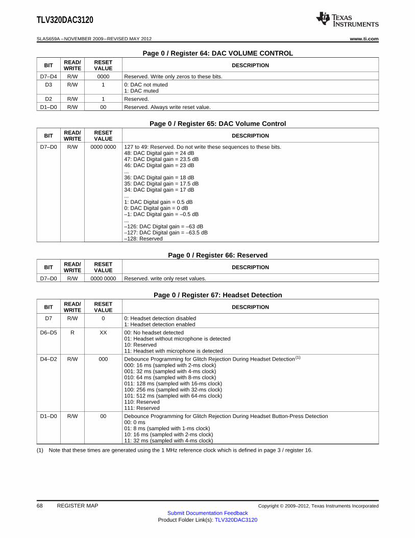
TLV320DAC3120
SLAS659A –NOVEMBER 2009–REVISED MAY 2012 www.ti.com
Page 0 / Register 64: DAC VOLUME CONTROLREAD/ RESETBIT DESCRIPTIONWRITE VALUE
D7–D4 R/W 0000 Reserved. Write only zeros to these bits.
D3 R/W 1 0: DAC not muted1: DAC muted
D2 R/W 1 Reserved.
D1–D0 R/W 00 Reserved. Always write reset value.
Page 0 / Register 65: DAC Volume ControlREAD/ RESETBIT DESCRIPTIONWRITE VALUE
D7–D0 R/W 0000 0000 127 to 49: Reserved. Do not write these sequences to these bits.48: DAC Digital gain = 24 dB47: DAC Digital gain = 23.5 dB46: DAC Digital gain = 23 dB...36: DAC Digital gain = 18 dB35: DAC Digital gain = 17.5 dB34: DAC Digital gain = 17 dB...1: DAC Digital gain = 0.5 dB0: DAC Digital gain = 0 dB–1: DAC Digital gain = –0.5 dB...–126: DAC Digital gain = –63 dB–127: DAC Digital gain = –63.5 dB–128: Reserved
Page 0 / Register 66: ReservedREAD/ RESETBIT DESCRIPTIONWRITE VALUE
D7–D0 R/W 0000 0000 Reserved. write only reset values.
Page 0 / Register 67: Headset DetectionREAD/ RESETBIT DESCRIPTIONWRITE VALUE
D7 R/W 0 0: Headset detection disabled1: Headset detection enabled
D6–D5 R XX 00: No headset detected01: Headset without microphone is detected10: Reserved11: Headset with microphone is detected
D4–D2 R/W 000 Debounce Programming for Glitch Rejection During Headset Detection (1)
000: 16 ms (sampled with 2-ms clock)001: 32 ms (sampled with 4-ms clock)010: 64 ms (sampled with 8-ms clock)011: 128 ms (sampled with 16-ms clock)100: 256 ms (sampled with 32-ms clock)101: 512 ms (sampled with 64-ms clock)110: Reserved111: Reserved
D1–D0 R/W 00 Debounce Programming for Glitch Rejection During Headset Button-Press Detection00: 0 ms01: 8 ms (sampled with 1-ms clock)10: 16 ms (sampled with 2-ms clock)11: 32 ms (sampled with 4-ms clock)
(1) Note that these times are generated using the 1 MHz reference clock which is defined in page 3 / register 16.
68 REGISTER MAP Copyright © 2009–2012, Texas Instruments Incorporated
Submit Documentation FeedbackProduct Folder Link(s): TLV320DAC3120
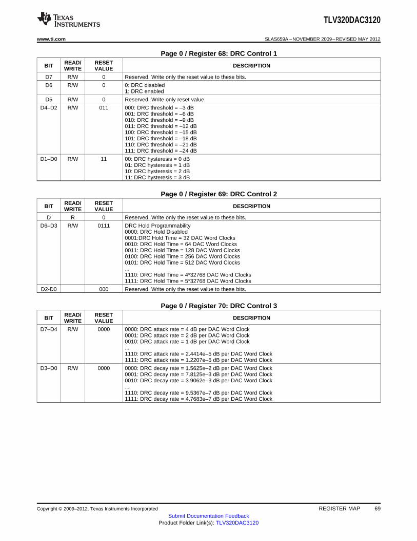
TLV320DAC3120
www.ti.com SLAS659A –NOVEMBER 2009–REVISED MAY 2012
Page 0 / Register 68: DRC Control 1READ/ RESETBIT DESCRIPTIONWRITE VALUE
D7 R/W 0 Reserved. Write only the reset value to these bits.
D6 R/W 0 0: DRC disabled1: DRC enabled
D5 R/W 0 Reserved. Write only reset value.
D4–D2 R/W 011 000: DRC threshold = –3 dB001: DRC threshold = –6 dB010: DRC threshold = –9 dB011: DRC threshold = –12 dB100: DRC threshold = –15 dB101: DRC threshold = –18 dB110: DRC threshold = –21 dB111: DRC threshold = –24 dB
D1–D0 R/W 11 00: DRC hysteresis = 0 dB01: DRC hysteresis = 1 dB10: DRC hysteresis = 2 dB11: DRC hysteresis = 3 dB
Page 0 / Register 69: DRC Control 2READ/ RESETBIT DESCRIPTIONWRITE VALUE
D R 0 Reserved. Write only the reset value to these bits.
D6–D3 R/W 0111 DRC Hold Programmability0000: DRC Hold Disabled0001:DRC Hold Time = 32 DAC Word Clocks0010: DRC Hold Time = 64 DAC Word Clocks0011: DRC Hold Time = 128 DAC Word Clocks0100: DRC Hold Time = 256 DAC Word Clocks0101: DRC Hold Time = 512 DAC Word Clocks...1110: DRC Hold Time = 4*32768 DAC Word Clocks1111: DRC Hold Time = 5*32768 DAC Word Clocks
D2-D0 000 Reserved. Write only the reset value to these bits.
Page 0 / Register 70: DRC Control 3READ/ RESETBIT DESCRIPTIONWRITE VALUE
D7–D4 R/W 0000 0000: DRC attack rate = 4 dB per DAC Word Clock0001: DRC attack rate = 2 dB per DAC Word Clock0010: DRC attack rate = 1 dB per DAC Word Clock...1110: DRC attack rate = 2.4414e–5 dB per DAC Word Clock1111: DRC attack rate = 1.2207e–5 dB per DAC Word Clock
D3–D0 R/W 0000 0000: DRC decay rate = 1.5625e–2 dB per DAC Word Clock0001: DRC decay rate = 7.8125e–3 dB per DAC Word Clock0010: DRC decay rate = 3.9062e–3 dB per DAC Word Clock...1110: DRC decay rate = 9.5367e–7 dB per DAC Word Clock1111: DRC decay rate = 4.7683e–7 dB per DAC Word Clock
Copyright © 2009–2012, Texas Instruments Incorporated REGISTER MAP 69Submit Documentation Feedback
Product Folder Link(s): TLV320DAC3120
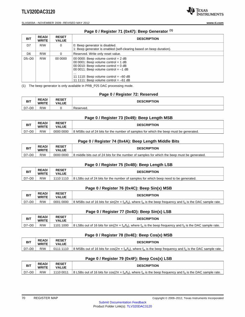
TLV320DAC3120
SLAS659A –NOVEMBER 2009–REVISED MAY 2012 www.ti.com
Page 0 / Register 71 (0x47): Beep Generator (1)
READ/ RESETBIT DESCRIPTIONWRITE VALUE
D7 R/W 0 0: Beep generator is disabled.1: Beep generator is enabled (self-clearing based on beep duration).
D6 R/W 0 Reserved. Write only reset value.
D5–D0 R/W 00 0000 00 0000: Beep volume control = 2 dB00 0001: Beep volume control = 1 dB00 0010: Beep volume control = 0 dB00 0011: Beep volume control = –1 dB...11 1110: Beep volume control = –60 dB11 1111: Beep volume control = –61 dB
(1) The beep generator is only available in PRB_P25 DAC processing mode.
Page 0 / Register 72: ReservedREAD/ RESETBIT DESCRIPTIONWRITE VALUE
D7–D0 R/W 0 Reserved.
Page 0 / Register 73 (0x49): Beep Length MSBREAD/ RESETBIT DESCRIPTIONWRITE VALUE
D7–D0 R/W 0000 0000 8 MSBs out of 24 bits for the number of samples for which the beep must be generated.
Page 0 / Register 74 (0x4A): Beep Length Middle BitsREAD/ RESETBIT DESCRIPTIONWRITE VALUE
D7–D0 R/W 0000 0000 8 middle bits out of 24 bits for the number of samples for which the beep must be generated.
Page 0 / Register 75 (0x4B): Beep Length LSBREAD/ RESETBIT DESCRIPTIONWRITE VALUE
D7–D0 R/W 1110 1110 8 LSBs out of 24 bits for the number of samples for which beep need to be generated.
Page 0 / Register 76 (0x4C): Beep Sin(x) MSBREAD/ RESETBIT DESCRIPTIONWRITE VALUE
D7–D0 R/W 0001 0000 8 MSBs out of 16 bits for sin(2π × fin/fS), where fin is the beep frequency and fS is the DAC sample rate.
Page 0 / Register 77 (0x4D): Beep Sin(x) LSBREAD/ RESETBIT DESCRIPTIONWRITE VALUE
D7–D0 R/W 1101 1000 8 LSBs out of 16 bits for sin(2π × fin/fS), where fin is the beep frequency and fS is the DAC sample rate.
Page 0 / Register 78 (0x4E): Beep Cos(x) MSBREAD/ RESETBIT DESCRIPTIONWRITE VALUE
D7–D0 R/W 0111 1110 8 MSBs out of 16 bits for cos(2π × fin/fS), where fin is the beep frequency and fS is the DAC sample rate.
Page 0 / Register 79 (0x4F): Beep Cos(x) LSBREAD/ RESETBIT DESCRIPTIONWRITE VALUE
D7–D0 R/W 1110 0011 8 LSBs out of 16 bits for cos(2π × fin/fS), where fin is the beep frequency and fS is the DAC sample rate.
70 REGISTER MAP Copyright © 2009–2012, Texas Instruments Incorporated
Submit Documentation FeedbackProduct Folder Link(s): TLV320DAC3120
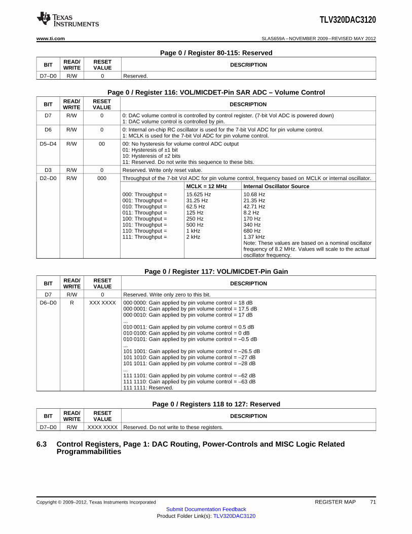
TLV320DAC3120
www.ti.com SLAS659A –NOVEMBER 2009–REVISED MAY 2012
Page 0 / Register 80-115: ReservedREAD/ RESETBIT DESCRIPTIONWRITE VALUE
D7–D0 R/W 0 Reserved.
Page 0 / Register 116: VOL/MICDET-Pin SAR ADC – Volume ControlREAD/ RESETBIT DESCRIPTIONWRITE VALUE
D7 R/W 0 0: DAC volume control is controlled by control register. (7-bit Vol ADC is powered down)1: DAC volume control is controlled by pin.
D6 R/W 0 0: Internal on-chip RC oscillator is used for the 7-bit Vol ADC for pin volume control.1: MCLK is used for the 7-bit Vol ADC for pin volume control.
D5–D4 R/W 00 00: No hysteresis for volume control ADC output01: Hysteresis of ±1 bit10: Hysteresis of ±2 bits11: Reserved. Do not write this sequence to these bits.
D3 R/W 0 Reserved. Write only reset value.
D2–D0 R/W 000 Throughput of the 7-bit Vol ADC for pin volume control, frequency based on MCLK or internal oscillator.
MCLK = 12 MHz Internal Oscillator Source
000: Throughput = 15.625 Hz 10.68 Hz001: Throughput = 31.25 Hz 21.35 Hz010: Throughput = 62.5 Hz 42.71 Hz011: Throughput = 125 Hz 8.2 Hz100: Throughput = 250 Hz 170 Hz101: Throughput = 500 Hz 340 Hz110: Throughput = 1 kHz 680 Hz111: Throughput = 2 kHz 1.37 kHz
Note: These values are based on a nominal oscillatorfrequency of 8.2 MHz. Values will scale to the actualoscillator frequency.
Page 0 / Register 117: VOL/MICDET-Pin GainREAD/ RESETBIT DESCRIPTIONWRITE VALUE
D7 R/W 0 Reserved. Write only zero to this bit.
D6–D0 R XXX XXXX 000 0000: Gain applied by pin volume control = 18 dB000 0001: Gain applied by pin volume control = 17.5 dB000 0010: Gain applied by pin volume control = 17 dB...010 0011: Gain applied by pin volume control = 0.5 dB010 0100: Gain applied by pin volume control = 0 dB010 0101: Gain applied by pin volume control = –0.5 dB...101 1001: Gain applied by pin volume control = –26.5 dB101 1010: Gain applied by pin volume control = –27 dB101 1011: Gain applied by pin volume control = –28 dB...111 1101: Gain applied by pin volume control = –62 dB111 1110: Gain applied by pin volume control = –63 dB111 1111: Reserved.
Page 0 / Registers 118 to 127: ReservedREAD/ RESETBIT DESCRIPTIONWRITE VALUE
D7–D0 R/W XXXX XXXX Reserved. Do not write to these registers.
6.3 Control Registers, Page 1: DAC Routing, Power-Controls and MISC Logic RelatedProgrammabilities
Copyright © 2009–2012, Texas Instruments Incorporated REGISTER MAP 71Submit Documentation Feedback
Product Folder Link(s): TLV320DAC3120
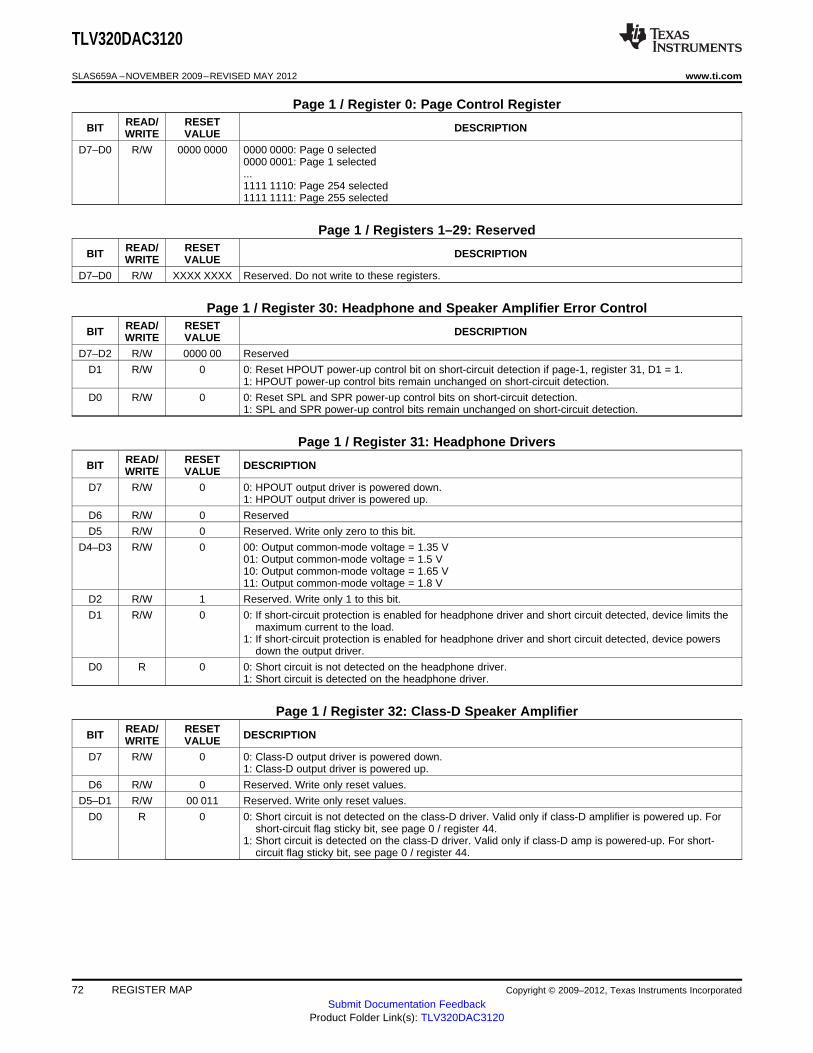
TLV320DAC3120
SLAS659A –NOVEMBER 2009–REVISED MAY 2012 www.ti.com
Page 1 / Register 0: Page Control RegisterREAD/ RESETBIT DESCRIPTIONWRITE VALUE
D7–D0 R/W 0000 0000 0000 0000: Page 0 selected0000 0001: Page 1 selected...1111 1110: Page 254 selected1111 1111: Page 255 selected
Page 1 / Registers 1–29: ReservedREAD/ RESETBIT DESCRIPTIONWRITE VALUE
D7–D0 R/W XXXX XXXX Reserved. Do not write to these registers.
Page 1 / Register 30: Headphone and Speaker Amplifier Error ControlREAD/ RESETBIT DESCRIPTIONWRITE VALUE
D7–D2 R/W 0000 00 Reserved
D1 R/W 0 0: Reset HPOUT power-up control bit on short-circuit detection if page-1, register 31, D1 = 1.1: HPOUT power-up control bits remain unchanged on short-circuit detection.
D0 R/W 0 0: Reset SPL and SPR power-up control bits on short-circuit detection.1: SPL and SPR power-up control bits remain unchanged on short-circuit detection.
Page 1 / Register 31: Headphone DriversREAD/ RESETBIT DESCRIPTIONWRITE VALUE
D7 R/W 0 0: HPOUT output driver is powered down.1: HPOUT output driver is powered up.
D6 R/W 0 Reserved
D5 R/W 0 Reserved. Write only zero to this bit.
D4–D3 R/W 0 00: Output common-mode voltage = 1.35 V01: Output common-mode voltage = 1.5 V10: Output common-mode voltage = 1.65 V11: Output common-mode voltage = 1.8 V
D2 R/W 1 Reserved. Write only 1 to this bit.
D1 R/W 0 0: If short-circuit protection is enabled for headphone driver and short circuit detected, device limits themaximum current to the load.
1: If short-circuit protection is enabled for headphone driver and short circuit detected, device powersdown the output driver.
D0 R 0 0: Short circuit is not detected on the headphone driver.1: Short circuit is detected on the headphone driver.
Page 1 / Register 32: Class-D Speaker AmplifierREAD/ RESETBIT DESCRIPTIONWRITE VALUE
D7 R/W 0 0: Class-D output driver is powered down.1: Class-D output driver is powered up.
D6 R/W 0 Reserved. Write only reset values.
D5–D1 R/W 00 011 Reserved. Write only reset values.
D0 R 0 0: Short circuit is not detected on the class-D driver. Valid only if class-D amplifier is powered up. Forshort-circuit flag sticky bit, see page 0 / register 44.
1: Short circuit is detected on the class-D driver. Valid only if class-D amp is powered-up. For short-circuit flag sticky bit, see page 0 / register 44.
72 REGISTER MAP Copyright © 2009–2012, Texas Instruments Incorporated
Submit Documentation FeedbackProduct Folder Link(s): TLV320DAC3120
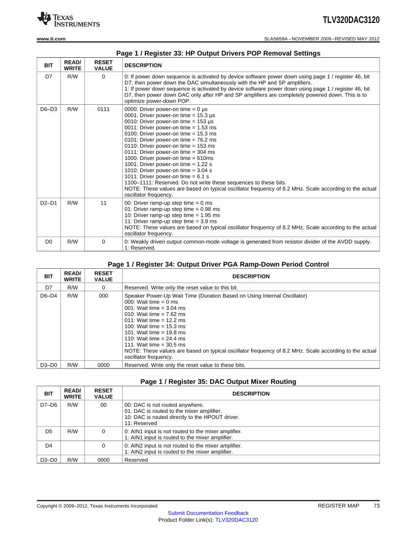
TLV320DAC3120
www.ti.com SLAS659A –NOVEMBER 2009–REVISED MAY 2012
Page 1 / Register 33: HP Output Drivers POP Removal SettingsREAD/ RESETBIT DESCRIPTIONWRITE VALUE
D7 R/W 0 0: If power down sequence is activated by device software power down using page 1 / register 46, bitD7, then power down the DAC simultaneously with the HP and SP amplifiers.1: If power down sequence is activated by device software power down using page 1 / register 46, bitD7, then power down DAC only after HP and SP amplifiers are completely powered down. This is tooptimize power-down POP.
D6–D3 R/W 0111 0000: Driver power-on time = 0 μs0001: Driver power-on time = 15.3 μs0010: Driver power-on time = 153 μs0011: Driver power-on time = 1.53 ms0100: Driver power-on time = 15.3 ms0101: Driver power-on time = 76.2 ms0110: Driver power-on time = 153 ms0111: Driver power-on time = 304 ms1000: Driver power-on time = 610ms1001: Driver power-on time = 1.22 s1010: Driver power-on time = 3.04 s1011: Driver power-on time = 6.1 s1100–1111: Reserved. Do not write these sequences to these bits.NOTE: These values are based on typical oscillator frequency of 8.2 MHz. Scale according to the actualoscillator frequency.
D2–D1 R/W 11 00: Driver ramp-up step time = 0 ms01: Driver ramp-up step time = 0.98 ms10: Driver ramp-up step time = 1.95 ms11: Driver ramp-up step time = 3.9 msNOTE: These values are based on typical oscillator frequency of 8.2 MHz. Scale according to the actualoscillator frequency.
D0 R/W 0 0: Weakly driven output common-mode voltage is generated from resistor divider of the AVDD supply.1: Reserved.
Page 1 / Register 34: Output Driver PGA Ramp-Down Period ControlREAD/ RESETBIT DESCRIPTIONWRITE VALUE
D7 R/W 0 Reserved. Write only the reset value to this bit.
D6–D4 R/W 000 Speaker Power-Up Wait Time (Duration Based on Using Internal Oscillator)000: Wait time = 0 ms001: Wait time = 3.04 ms010: Wait time = 7.62 ms011: Wait time = 12.2 ms100: Wait time = 15.3 ms101: Wait time = 19.8 ms110: Wait time = 24.4 ms111: Wait time = 30.5 msNOTE: These values are based on typical oscillator frequency of 8.2 MHz. Scale according to the actualoscillator frequency.
D3–D0 R/W 0000 Reserved. Write only the reset value to these bits.
Page 1 / Register 35: DAC Output Mixer RoutingREAD/ RESETBIT DESCRIPTIONWRITE VALUE
D7–D6 R/W 00 00: DAC is not routed anywhere.01: DAC is routed to the mixer amplifier.10: DAC is routed directly to the HPOUT driver.11: Reserved
D5 R/W 0 0: AIN1 input is not routed to the mixer amplifier.1: AIN1 input is routed to the mixer amplifier.
D4 0 0: AIN2 input is not routed to the mixer amplifier.1: AIN2 input is routed to the mixer amplifier.
D3–D0 R/W 0000 Reserved
Copyright © 2009–2012, Texas Instruments Incorporated REGISTER MAP 73Submit Documentation Feedback
Product Folder Link(s): TLV320DAC3120
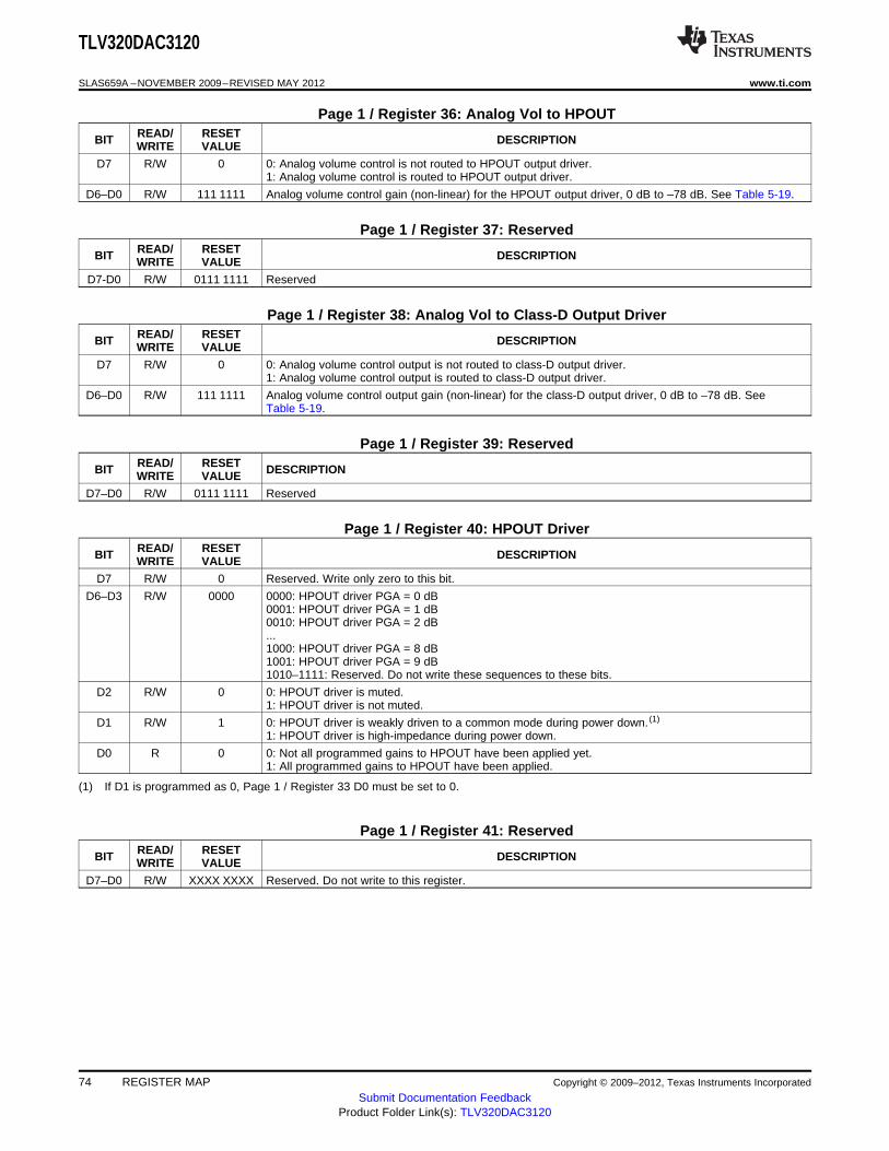
TLV320DAC3120
SLAS659A –NOVEMBER 2009–REVISED MAY 2012 www.ti.com
Page 1 / Register 36: Analog Vol to HPOUTREAD/ RESETBIT DESCRIPTIONWRITE VALUE
D7 R/W 0 0: Analog volume control is not routed to HPOUT output driver.1: Analog volume control is routed to HPOUT output driver.
D6–D0 R/W 111 1111 Analog volume control gain (non-linear) for the HPOUT output driver, 0 dB to –78 dB. See Table 5-19.
Page 1 / Register 37: ReservedREAD/ RESETBIT DESCRIPTIONWRITE VALUE
D7-D0 R/W 0111 1111 Reserved
Page 1 / Register 38: Analog Vol to Class-D Output DriverREAD/ RESETBIT DESCRIPTIONWRITE VALUE
D7 R/W 0 0: Analog volume control output is not routed to class-D output driver.1: Analog volume control output is routed to class-D output driver.
D6–D0 R/W 111 1111 Analog volume control output gain (non-linear) for the class-D output driver, 0 dB to –78 dB. SeeTable 5-19.
Page 1 / Register 39: ReservedREAD/ RESETBIT DESCRIPTIONWRITE VALUE
D7–D0 R/W 0111 1111 Reserved
Page 1 / Register 40: HPOUT DriverREAD/ RESETBIT DESCRIPTIONWRITE VALUE
D7 R/W 0 Reserved. Write only zero to this bit.
D6–D3 R/W 0000 0000: HPOUT driver PGA = 0 dB0001: HPOUT driver PGA = 1 dB0010: HPOUT driver PGA = 2 dB...1000: HPOUT driver PGA = 8 dB1001: HPOUT driver PGA = 9 dB1010–1111: Reserved. Do not write these sequences to these bits.
D2 R/W 0 0: HPOUT driver is muted.1: HPOUT driver is not muted.
D1 R/W 1 0: HPOUT driver is weakly driven to a common mode during power down. (1)
1: HPOUT driver is high-impedance during power down.
D0 R 0 0: Not all programmed gains to HPOUT have been applied yet.1: All programmed gains to HPOUT have been applied.
(1) If D1 is programmed as 0, Page 1 / Register 33 D0 must be set to 0.
Page 1 / Register 41: ReservedREAD/ RESETBIT DESCRIPTIONWRITE VALUE
D7–D0 R/W XXXX XXXX Reserved. Do not write to this register.
74 REGISTER MAP Copyright © 2009–2012, Texas Instruments Incorporated
Submit Documentation FeedbackProduct Folder Link(s): TLV320DAC3120
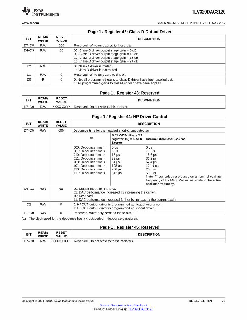
TLV320DAC3120
www.ti.com SLAS659A –NOVEMBER 2009–REVISED MAY 2012
Page 1 / Register 42: Class-D Output DriverREAD/ RESETBIT DESCRIPTIONWRITE VALUE
D7–D5 R/W 000 Reserved. Write only zeros to these bits.
D4–D3 R/W 00 00: Class-D driver output stage gain = 6 dB01: Class-D driver output stage gain = 12 dB10: Class-D driver output stage gain = 18 dB11: Class-D driver output stage gain = 24 dB
D2 R/W 0 0: Class-D driver is muted.1: Class-D driver is not muted.
D1 R/W 0 Reserved. Write only zero to this bit.
D0 R 0 0: Not all programmed gains to class-D driver have been applied yet.1: All programmed gains to class-D driver have been applied.
Page 1 / Register 43: ReservedREAD/ RESETBIT DESCRIPTIONWRITE VALUE
D7–D0 R/W XXXX XXXX Reserved. Do not wite to this register.
Page 1 / Register 44: HP Driver ControlREAD/ RESETBIT DESCRIPTIONWRITE VALUE
D7–D5 R/W 000 Debounce time for the headset short-circuit detection
MCLK/DIV (Page 3 /(1) register 16) = 1-MHz Internal Oscillator Source
Source
000: Debounce time = 0 μs 0 μs001: Debounce time = 8 μs 7.8 μs010: Debounce time = 16 μs 15.6 μs011: Debounce time = 32 μs 31.2 μs100: Debounce time = 64 μs 62.4 μs101: Debounce time = 128 μs 124.9 μs110: Debounce time = 256 μs 250 μs111: Debounce time = 512 μs 500 μs
Note: These values are based on a nominal oscillatorfrequency of 8.2 MHz. Values will scale to the actualoscillator frequency.
D4–D3 R/W 00 00: Default mode for the DAC01: DAC performance increased by increasing the current10: Reserved11: DAC performance increased further by increasing the current again
D2 R/W 0 0: HPOUT output driver is programmed as headphone driver.1: HPOUT output driver is programmed as lineout driver.
D1–D0 R/W 0 Reserved. Write only zeros to these bits.
(1) The clock used for the debounce has a clock period = debounce duration/8.
Page 1 / Register 45: ReservedREAD/ RESETBIT DESCRIPTIONWRITE VALUE
D7–D0 R/W XXXX XXXX Reserved. Do not write to these registers.
Copyright © 2009–2012, Texas Instruments Incorporated REGISTER MAP 75Submit Documentation Feedback
Product Folder Link(s): TLV320DAC3120
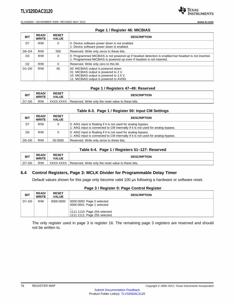
TLV320DAC3120
SLAS659A –NOVEMBER 2009–REVISED MAY 2012 www.ti.com
Page 1 / Register 46: MICBIASREAD/ RESETBIT DESCRIPTIONWRITE VALUE
D7 R/W 0 0: Device software power down is not enabled.1: Device software power down is enabled.
D6–D4 R/W 000 Reserved. Write only zeros to these bits.
D3 R/W 0 0: Programmed MICBIAS is not powered up if headset detection is enabled but headset is not inserted.1: Programmed MICBIAS is powered up even if headset is not inserted.
D2 R/W 0 Reserved. Write only zero to this bit.
D1–D0 R/W 00 00: MICBIAS output is powered down.01: MICBIAS output is powered to 2 V.10: MICBIAS output is powered to 2.5 V.11: MICBIAS output is powered to AVDD.
Page 1 / Registers 47–49: ReservedREAD/ RESETBIT DESCRIPTIONWRITE VALUE
D7–D0 R/W XXXX XXXX Reserved. Write only the reset value to these bits.
Table 6-3. Page 1 / Register 50: Input CM SettingsREAD/ RESETBIT DESCRIPTIONWRITE VALUE
D7 R/W 0 0: AIN1 input is floating if it is not used for analog bypass.1: AIN1 input is connected to CM internally if it is not used for analog bypass.
D6 R/W 0 0: AIN2 input is floating if it is not used for analog bypass.1: AIN2 input is connected to CM internally if it is not used for analog bypass.
D5–D0 R/W 00 0000 Reserved. Write only zeros to these bits.
Table 6-4. Page 1 / Registers 51–127: ReservedREAD/ RESETBIT DESCRIPTIONWRITE VALUE
D7–D0 R/W XXXX XXXX Reserved. Write only the reset value to these bits.
6.4 Control Registers, Page 3: MCLK Divider for Programmable Delay Timer
Default values shown for this page only become valid 100 μs following a hardware or software reset.
Page 3 / Register 0: Page Control RegisterREAD/ RESETBIT DESCRIPTIONWRITE VALUE
D7–D0 R/W 0000 0000 0000 0000: Page 0 selected0000 0001: Page 1 selected...1111 1110: Page 254 selected1111 1111: Page 255 selected
The only register used in page 3 is register 16. The remaining page 3 registers are reserved and shouldnot be written to.
76 REGISTER MAP Copyright © 2009–2012, Texas Instruments Incorporated
Submit Documentation FeedbackProduct Folder Link(s): TLV320DAC3120
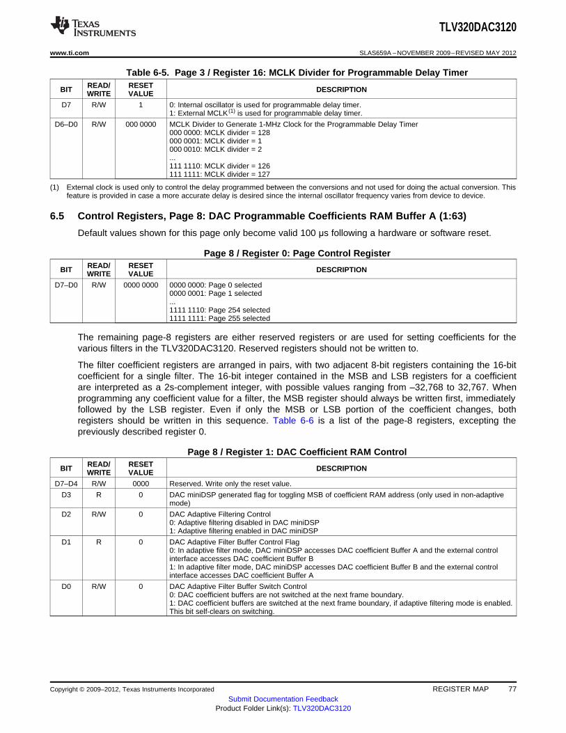
TLV320DAC3120
www.ti.com SLAS659A –NOVEMBER 2009–REVISED MAY 2012
Table 6-5. Page 3 / Register 16: MCLK Divider for Programmable Delay TimerREAD/ RESETBIT DESCRIPTIONWRITE VALUE
D7 R/W 1 0: Internal oscillator is used for programmable delay timer.1: External MCLK (1) is used for programmable delay timer.
D6–D0 R/W 000 0000 MCLK Divider to Generate 1-MHz Clock for the Programmable Delay Timer000 0000: MCLK divider = 128000 0001: MCLK divider = 1000 0010: MCLK divider = 2...111 1110: MCLK divider = 126111 1111: MCLK divider = 127
(1) External clock is used only to control the delay programmed between the conversions and not used for doing the actual conversion. Thisfeature is provided in case a more accurate delay is desired since the internal oscillator frequency varies from device to device.
6.5 Control Registers, Page 8: DAC Programmable Coefficients RAM Buffer A (1:63)
Default values shown for this page only become valid 100 μs following a hardware or software reset.
Page 8 / Register 0: Page Control RegisterREAD/ RESETBIT DESCRIPTIONWRITE VALUE
D7–D0 R/W 0000 0000 0000 0000: Page 0 selected0000 0001: Page 1 selected...1111 1110: Page 254 selected1111 1111: Page 255 selected
The remaining page-8 registers are either reserved registers or are used for setting coefficients for thevarious filters in the TLV320DAC3120. Reserved registers should not be written to.
The filter coefficient registers are arranged in pairs, with two adjacent 8-bit registers containing the 16-bitcoefficient for a single filter. The 16-bit integer contained in the MSB and LSB registers for a coefficientare interpreted as a 2s-complement integer, with possible values ranging from –32,768 to 32,767. Whenprogramming any coefficient value for a filter, the MSB register should always be written first, immediatelyfollowed by the LSB register. Even if only the MSB or LSB portion of the coefficient changes, bothregisters should be written in this sequence. Table 6-6 is a list of the page-8 registers, excepting thepreviously described register 0.
Page 8 / Register 1: DAC Coefficient RAM ControlREAD/ RESETBIT DESCRIPTIONWRITE VALUE
D7–D4 R/W 0000 Reserved. Write only the reset value.
D3 R 0 DAC miniDSP generated flag for toggling MSB of coefficient RAM address (only used in non-adaptivemode)
D2 R/W 0 DAC Adaptive Filtering Control0: Adaptive filtering disabled in DAC miniDSP1: Adaptive filtering enabled in DAC miniDSP
D1 R 0 DAC Adaptive Filter Buffer Control Flag0: In adaptive filter mode, DAC miniDSP accesses DAC coefficient Buffer A and the external controlinterface accesses DAC coefficient Buffer B1: In adaptive filter mode, DAC miniDSP accesses DAC coefficient Buffer B and the external controlinterface accesses DAC coefficient Buffer A
D0 R/W 0 DAC Adaptive Filter Buffer Switch Control0: DAC coefficient buffers are not switched at the next frame boundary.1: DAC coefficient buffers are switched at the next frame boundary, if adaptive filtering mode is enabled.This bit self-clears on switching.
Copyright © 2009–2012, Texas Instruments Incorporated REGISTER MAP 77Submit Documentation Feedback
Product Folder Link(s): TLV320DAC3120
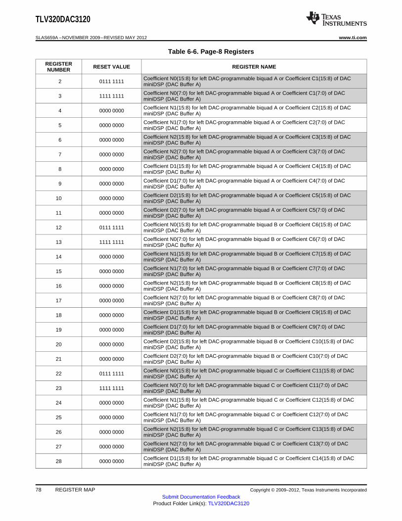
TLV320DAC3120
SLAS659A –NOVEMBER 2009–REVISED MAY 2012 www.ti.com
Table 6-6. Page-8 Registers
REGISTER RESET VALUE REGISTER NAMENUMBER
Coefficient N0(15:8) for left DAC-programmable biquad A or Coefficient C1(15:8) of DAC2 0111 1111 miniDSP (DAC Buffer A)
Coefficient N0(7:0) for left DAC-programmable biquad A or Coefficient C1(7:0) of DAC3 1111 1111 miniDSP (DAC Buffer A)
Coefficient N1(15:8) for left DAC-programmable biquad A or Coefficient C2(15:8) of DAC4 0000 0000 miniDSP (DAC Buffer A)
Coefficient N1(7:0) for left DAC-programmable biquad A or Coefficient C2(7:0) of DAC5 0000 0000 miniDSP (DAC Buffer A)
Coefficient N2(15:8) for left DAC-programmable biquad A or Coefficient C3(15:8) of DAC6 0000 0000 miniDSP (DAC Buffer A)
Coefficient N2(7:0) for left DAC-programmable biquad A or Coefficient C3(7:0) of DAC7 0000 0000 miniDSP (DAC Buffer A)
Coefficient D1(15:8) for left DAC-programmable biquad A or Coefficient C4(15:8) of DAC8 0000 0000 miniDSP (DAC Buffer A)
Coefficient D1(7:0) for left DAC-programmable biquad A or Coefficient C4(7:0) of DAC9 0000 0000 miniDSP (DAC Buffer A)
Coefficient D2(15:8) for left DAC-programmable biquad A or Coefficient C5(15:8) of DAC10 0000 0000 miniDSP (DAC Buffer A)
Coefficient D2(7:0) for left DAC-programmable biquad A or Coefficient C5(7:0) of DAC11 0000 0000 miniDSP (DAC Buffer A)
Coefficient N0(15:8) for left DAC-programmable biquad B or Coefficient C6(15:8) of DAC12 0111 1111 miniDSP (DAC Buffer A)
Coefficient N0(7:0) for left DAC-programmable biquad B or Coefficient C6(7:0) of DAC13 1111 1111 miniDSP (DAC Buffer A)
Coefficient N1(15:8) for left DAC-programmable biquad B or Coefficient C7(15:8) of DAC14 0000 0000 miniDSP (DAC Buffer A)
Coefficient N1(7:0) for left DAC-programmable biquad B or Coefficient C7(7:0) of DAC15 0000 0000 miniDSP (DAC Buffer A)
Coefficient N2(15:8) for left DAC-programmable biquad B or Coefficient C8(15:8) of DAC16 0000 0000 miniDSP (DAC Buffer A)
Coefficient N2(7:0) for left DAC-programmable biquad B or Coefficient C8(7:0) of DAC17 0000 0000 miniDSP (DAC Buffer A)
Coefficient D1(15:8) for left DAC-programmable biquad B or Coefficient C9(15:8) of DAC18 0000 0000 miniDSP (DAC Buffer A)
Coefficient D1(7:0) for left DAC-programmable biquad B or Coefficient C9(7:0) of DAC19 0000 0000 miniDSP (DAC Buffer A)
Coefficient D2(15:8) for left DAC-programmable biquad B or Coefficient C10(15:8) of DAC20 0000 0000 miniDSP (DAC Buffer A)
Coefficient D2(7:0) for left DAC-programmable biquad B or Coefficient C10(7:0) of DAC21 0000 0000 miniDSP (DAC Buffer A)
Coefficient N0(15:8) for left DAC-programmable biquad C or Coefficient C11(15:8) of DAC22 0111 1111 miniDSP (DAC Buffer A)
Coefficient N0(7:0) for left DAC-programmable biquad C or Coefficient C11(7:0) of DAC23 1111 1111 miniDSP (DAC Buffer A)
Coefficient N1(15:8) for left DAC-programmable biquad C or Coefficient C12(15:8) of DAC24 0000 0000 miniDSP (DAC Buffer A)
Coefficient N1(7:0) for left DAC-programmable biquad C or Coefficient C12(7:0) of DAC25 0000 0000 miniDSP (DAC Buffer A)
Coefficient N2(15:8) for left DAC-programmable biquad C or Coefficient C13(15:8) of DAC26 0000 0000 miniDSP (DAC Buffer A)
Coefficient N2(7:0) for left DAC-programmable biquad C or Coefficient C13(7:0) of DAC27 0000 0000 miniDSP (DAC Buffer A)
Coefficient D1(15:8) for left DAC-programmable biquad C or Coefficient C14(15:8) of DAC28 0000 0000 miniDSP (DAC Buffer A)
78 REGISTER MAP Copyright © 2009–2012, Texas Instruments Incorporated
Submit Documentation FeedbackProduct Folder Link(s): TLV320DAC3120
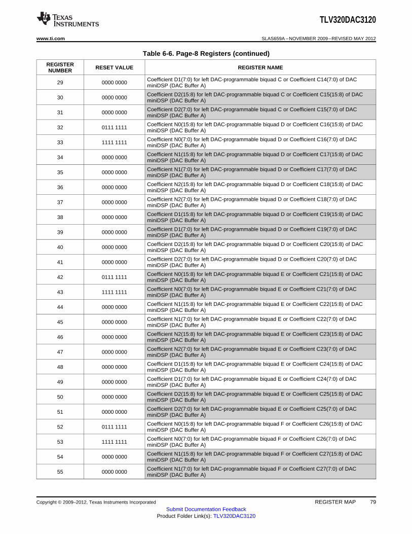
TLV320DAC3120
www.ti.com SLAS659A –NOVEMBER 2009–REVISED MAY 2012
Table 6-6. Page-8 Registers (continued)
REGISTER RESET VALUE REGISTER NAMENUMBER
Coefficient D1(7:0) for left DAC-programmable biquad C or Coefficient C14(7:0) of DAC29 0000 0000 miniDSP (DAC Buffer A)
Coefficient D2(15:8) for left DAC-programmable biquad C or Coefficient C15(15:8) of DAC30 0000 0000 miniDSP (DAC Buffer A)
Coefficient D2(7:0) for left DAC-programmable biquad C or Coefficient C15(7:0) of DAC31 0000 0000 miniDSP (DAC Buffer A)
Coefficient N0(15:8) for left DAC-programmable biquad D or Coefficient C16(15:8) of DAC32 0111 1111 miniDSP (DAC Buffer A)
Coefficient N0(7:0) for left DAC-programmable biquad D or Coefficient C16(7:0) of DAC33 1111 1111 miniDSP (DAC Buffer A)
Coefficient N1(15:8) for left DAC-programmable biquad D or Coefficient C17(15:8) of DAC34 0000 0000 miniDSP (DAC Buffer A)
Coefficient N1(7:0) for left DAC-programmable biquad D or Coefficient C17(7:0) of DAC35 0000 0000 miniDSP (DAC Buffer A)
Coefficient N2(15:8) for left DAC-programmable biquad D or Coefficient C18(15:8) of DAC36 0000 0000 miniDSP (DAC Buffer A)
Coefficient N2(7:0) for left DAC-programmable biquad D or Coefficient C18(7:0) of DAC37 0000 0000 miniDSP (DAC Buffer A)
Coefficient D1(15:8) for left DAC-programmable biquad D or Coefficient C19(15:8) of DAC38 0000 0000 miniDSP (DAC Buffer A)
Coefficient D1(7:0) for left DAC-programmable biquad D or Coefficient C19(7:0) of DAC39 0000 0000 miniDSP (DAC Buffer A)
Coefficient D2(15:8) for left DAC-programmable biquad D or Coefficient C20(15:8) of DAC40 0000 0000 miniDSP (DAC Buffer A)
Coefficient D2(7:0) for left DAC-programmable biquad D or Coefficient C20(7:0) of DAC41 0000 0000 miniDSP (DAC Buffer A)
Coefficient N0(15:8) for left DAC-programmable biquad E or Coefficient C21(15:8) of DAC42 0111 1111 miniDSP (DAC Buffer A)
Coefficient N0(7:0) for left DAC-programmable biquad E or Coefficient C21(7:0) of DAC43 1111 1111 miniDSP (DAC Buffer A)
Coefficient N1(15:8) for left DAC-programmable biquad E or Coefficient C22(15:8) of DAC44 0000 0000 miniDSP (DAC Buffer A)
Coefficient N1(7:0) for left DAC-programmable biquad E or Coefficient C22(7:0) of DAC45 0000 0000 miniDSP (DAC Buffer A)
Coefficient N2(15:8) for left DAC-programmable biquad E or Coefficient C23(15:8) of DAC46 0000 0000 miniDSP (DAC Buffer A)
Coefficient N2(7:0) for left DAC-programmable biquad E or Coefficient C23(7:0) of DAC47 0000 0000 miniDSP (DAC Buffer A)
Coefficient D1(15:8) for left DAC-programmable biquad E or Coefficient C24(15:8) of DAC48 0000 0000 miniDSP (DAC Buffer A)
Coefficient D1(7:0) for left DAC-programmable biquad E or Coefficient C24(7:0) of DAC49 0000 0000 miniDSP (DAC Buffer A)
Coefficient D2(15:8) for left DAC-programmable biquad E or Coefficient C25(15:8) of DAC50 0000 0000 miniDSP (DAC Buffer A)
Coefficient D2(7:0) for left DAC-programmable biquad E or Coefficient C25(7:0) of DAC51 0000 0000 miniDSP (DAC Buffer A)
Coefficient N0(15:8) for left DAC-programmable biquad F or Coefficient C26(15:8) of DAC52 0111 1111 miniDSP (DAC Buffer A)
Coefficient N0(7:0) for left DAC-programmable biquad F or Coefficient C26(7:0) of DAC53 1111 1111 miniDSP (DAC Buffer A)
Coefficient N1(15:8) for left DAC-programmable biquad F or Coefficient C27(15:8) of DAC54 0000 0000 miniDSP (DAC Buffer A)
Coefficient N1(7:0) for left DAC-programmable biquad F or Coefficient C27(7:0) of DAC55 0000 0000 miniDSP (DAC Buffer A)
Copyright © 2009–2012, Texas Instruments Incorporated REGISTER MAP 79Submit Documentation Feedback
Product Folder Link(s): TLV320DAC3120
TLV320DAC3120
SLAS659A –NOVEMBER 2009–REVISED MAY 2012 www.ti.com
Table 6-6. Page-8 Registers (continued)
REGISTER RESET VALUE REGISTER NAMENUMBER
Coefficient N2(15:8) for left DAC-programmable biquad F or Coefficient C28(15:8) of DAC56 0000 0000 miniDSP (DAC Buffer A)
Coefficient N2(7:0) for left DAC-programmable biquad F or Coefficient C28(7:0) of DAC57 0000 0000 miniDSP (DAC Buffer A)
Coefficient D1(15:8) for left DAC-programmable biquad F or Coefficient C29(15:8) of DAC58 0000 0000 miniDSP (DAC Buffer A)
Coefficient D1(7:0) for left DAC-programmable biquad F or Coefficient C29(7:0) of DAC59 0000 0000 miniDSP (DAC Buffer A)
Coefficient D2(15:8) for left DAC-programmable biquad F or Coefficient C30(15:8) of DAC60 0000 0000 miniDSP (DAC Buffer A)
Coefficient D2(7:0) for left DAC-programmable biquad F or Coefficient C30(7:0) of DAC61 0000 0000 miniDSP (DAC Buffer A)
62 0000 0000 Coefficient C31(15:8) of DAC miniDSP (DAC Buffer A)
63 0000 0000 Coefficient C31(7:0) of DAC miniDSP (DAC Buffer A)
Coefficient C32(15:8) of DAC miniDSP (DAC Buffer A)—also used for the 3D PGA for64 0000 0000 PRB_P23, PRB_P24 and PRB_P25
Coefficient C32(7:0) of DAC miniDSP (DAC Buffer A)—also used for the 3D PGA for65 0000 0000 PRB_P23, PRB_P24 and PRB_P25
66 0111 1111 Reserved.
67 1111 1111 Reserved.
68 0000 0000 Reserved.
69 0000 0000 Reserved.
70 0000 0000 Reserved.
71 0000 0000 Reserved.
72 0000 0000 Reserved.
73 0000 0000 Reserved.
74 0000 0000 Reserved.
75 0000 0000 Reserved.
76 0111 1111 Reserved.
77 1111 1111 Reserved.
78 0000 0000 Reserved.
79 0000 0000 Reserved.
80 0000 0000 Reserved.
81 0000 0000 Reserved.
82 0000 0000 Reserved.
83 0000 0000 Reserved.
84 0000 0000 Reserved.
85 0000 0000 Reserved.
86 0111 1111 Reserved.
87 1111 1111 Reserved.
88 0000 0000 Reserved.
89 0000 0000 Reserved.
90 0000 0000 Reserved.
91 0000 0000 Reserved.
92 0000 0000 Reserved.
93 0000 0000 Reserved.
94 0000 0000 Reserved.
95 0000 0000 Reserved.
96 0111 1111 Reserved.
80 REGISTER MAP Copyright © 2009–2012, Texas Instruments Incorporated
Submit Documentation FeedbackProduct Folder Link(s): TLV320DAC3120
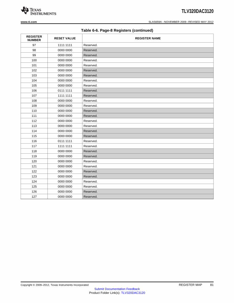
TLV320DAC3120
www.ti.com SLAS659A –NOVEMBER 2009–REVISED MAY 2012
Table 6-6. Page-8 Registers (continued)
REGISTER RESET VALUE REGISTER NAMENUMBER
97 1111 1111 Reserved.
98 0000 0000 Reserved.
99 0000 0000 Reserved.
100 0000 0000 Reserved.
101 0000 0000 Reserved.
102 0000 0000 Reserved.
103 0000 0000 Reserved.
104 0000 0000 Reserved.
105 0000 0000 Reserved.
106 0111 1111 Reserved.
107 1111 1111 Reserved.
108 0000 0000 Reserved.
109 0000 0000 Reserved.
110 0000 0000 Reserved.
111 0000 0000 Reserved.
112 0000 0000 Reserved.
113 0000 0000 Reserved.
114 0000 0000 Reserved.
115 0000 0000 Reserved.
116 0111 1111 Reserved.
117 1111 1111 Reserved.
118 0000 0000 Reserved.
119 0000 0000 Reserved.
120 0000 0000 Reserved.
121 0000 0000 Reserved.
122 0000 0000 Reserved.
123 0000 0000 Reserved.
124 0000 0000 Reserved.
125 0000 0000 Reserved.
126 0000 0000 Reserved.
127 0000 0000 Reserved.
Copyright © 2009–2012, Texas Instruments Incorporated REGISTER MAP 81Submit Documentation Feedback
Product Folder Link(s): TLV320DAC3120
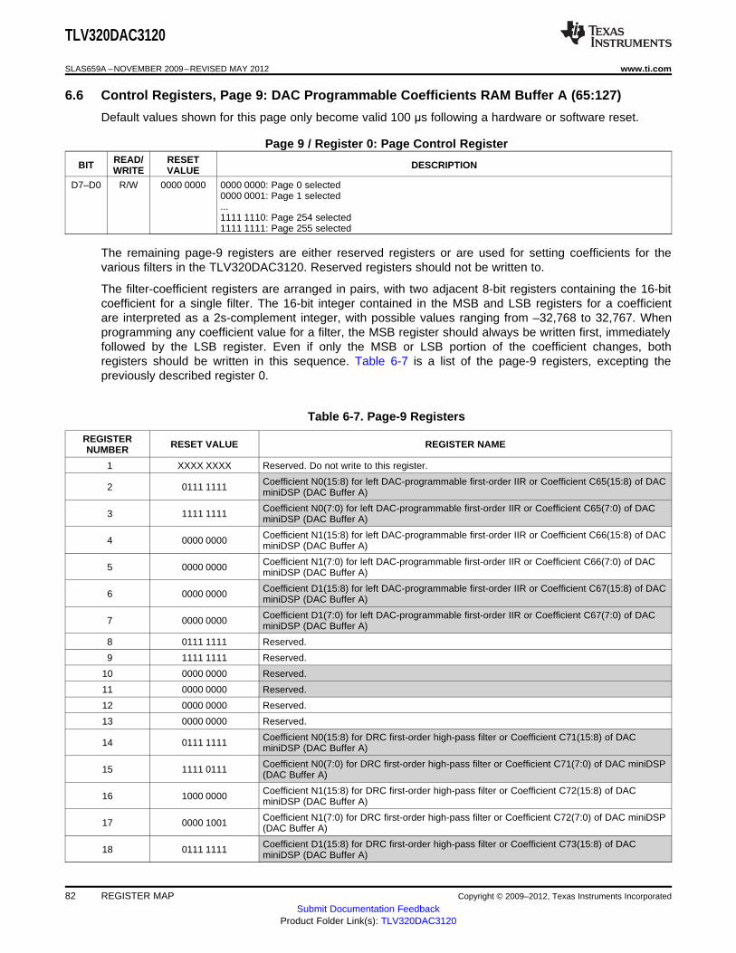
TLV320DAC3120
SLAS659A –NOVEMBER 2009–REVISED MAY 2012 www.ti.com
6.6 Control Registers, Page 9: DAC Programmable Coefficients RAM Buffer A (65:127)
Default values shown for this page only become valid 100 μs following a hardware or software reset.
Page 9 / Register 0: Page Control RegisterREAD/ RESETBIT DESCRIPTIONWRITE VALUE
D7–D0 R/W 0000 0000 0000 0000: Page 0 selected0000 0001: Page 1 selected...1111 1110: Page 254 selected1111 1111: Page 255 selected
The remaining page-9 registers are either reserved registers or are used for setting coefficients for thevarious filters in the TLV320DAC3120. Reserved registers should not be written to.
The filter-coefficient registers are arranged in pairs, with two adjacent 8-bit registers containing the 16-bitcoefficient for a single filter. The 16-bit integer contained in the MSB and LSB registers for a coefficientare interpreted as a 2s-complement integer, with possible values ranging from –32,768 to 32,767. Whenprogramming any coefficient value for a filter, the MSB register should always be written first, immediatelyfollowed by the LSB register. Even if only the MSB or LSB portion of the coefficient changes, bothregisters should be written in this sequence. Table 6-7 is a list of the page-9 registers, excepting thepreviously described register 0.
Table 6-7. Page-9 Registers
REGISTER RESET VALUE REGISTER NAMENUMBER
1 XXXX XXXX Reserved. Do not write to this register.
Coefficient N0(15:8) for left DAC-programmable first-order IIR or Coefficient C65(15:8) of DAC2 0111 1111 miniDSP (DAC Buffer A)
Coefficient N0(7:0) for left DAC-programmable first-order IIR or Coefficient C65(7:0) of DAC3 1111 1111 miniDSP (DAC Buffer A)
Coefficient N1(15:8) for left DAC-programmable first-order IIR or Coefficient C66(15:8) of DAC4 0000 0000 miniDSP (DAC Buffer A)
Coefficient N1(7:0) for left DAC-programmable first-order IIR or Coefficient C66(7:0) of DAC5 0000 0000 miniDSP (DAC Buffer A)
Coefficient D1(15:8) for left DAC-programmable first-order IIR or Coefficient C67(15:8) of DAC6 0000 0000 miniDSP (DAC Buffer A)
Coefficient D1(7:0) for left DAC-programmable first-order IIR or Coefficient C67(7:0) of DAC7 0000 0000 miniDSP (DAC Buffer A)
8 0111 1111 Reserved.
9 1111 1111 Reserved.
10 0000 0000 Reserved.
11 0000 0000 Reserved.
12 0000 0000 Reserved.
13 0000 0000 Reserved.
Coefficient N0(15:8) for DRC first-order high-pass filter or Coefficient C71(15:8) of DAC14 0111 1111 miniDSP (DAC Buffer A)
Coefficient N0(7:0) for DRC first-order high-pass filter or Coefficient C71(7:0) of DAC miniDSP15 1111 0111 (DAC Buffer A)
Coefficient N1(15:8) for DRC first-order high-pass filter or Coefficient C72(15:8) of DAC16 1000 0000 miniDSP (DAC Buffer A)
Coefficient N1(7:0) for DRC first-order high-pass filter or Coefficient C72(7:0) of DAC miniDSP17 0000 1001 (DAC Buffer A)
Coefficient D1(15:8) for DRC first-order high-pass filter or Coefficient C73(15:8) of DAC18 0111 1111 miniDSP (DAC Buffer A)
82 REGISTER MAP Copyright © 2009–2012, Texas Instruments Incorporated
Submit Documentation FeedbackProduct Folder Link(s): TLV320DAC3120
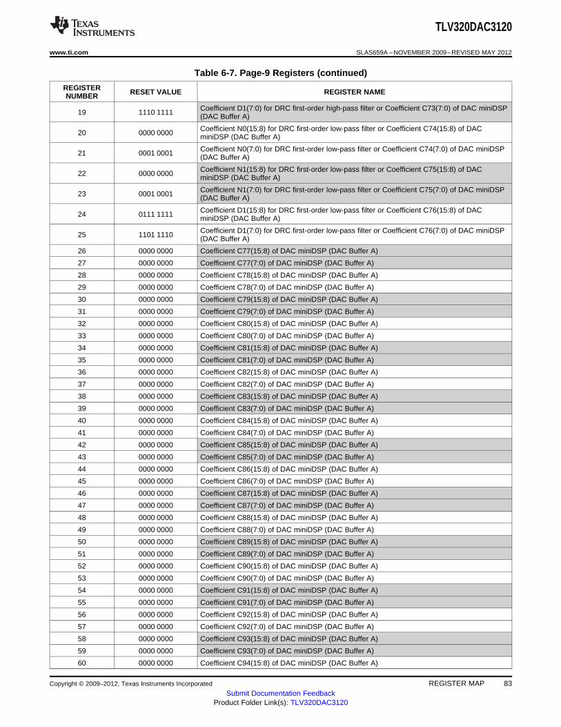
TLV320DAC3120
www.ti.com SLAS659A –NOVEMBER 2009–REVISED MAY 2012
Table 6-7. Page-9 Registers (continued)
REGISTER RESET VALUE REGISTER NAMENUMBER
Coefficient D1(7:0) for DRC first-order high-pass filter or Coefficient C73(7:0) of DAC miniDSP19 1110 1111 (DAC Buffer A)
Coefficient N0(15:8) for DRC first-order low-pass filter or Coefficient C74(15:8) of DAC20 0000 0000 miniDSP (DAC Buffer A)
Coefficient N0(7:0) for DRC first-order low-pass filter or Coefficient C74(7:0) of DAC miniDSP21 0001 0001 (DAC Buffer A)
Coefficient N1(15:8) for DRC first-order low-pass filter or Coefficient C75(15:8) of DAC22 0000 0000 miniDSP (DAC Buffer A)
Coefficient N1(7:0) for DRC first-order low-pass filter or Coefficient C75(7:0) of DAC miniDSP23 0001 0001 (DAC Buffer A)
Coefficient D1(15:8) for DRC first-order low-pass filter or Coefficient C76(15:8) of DAC24 0111 1111 miniDSP (DAC Buffer A)
Coefficient D1(7:0) for DRC first-order low-pass filter or Coefficient C76(7:0) of DAC miniDSP25 1101 1110 (DAC Buffer A)
26 0000 0000 Coefficient C77(15:8) of DAC miniDSP (DAC Buffer A)
27 0000 0000 Coefficient C77(7:0) of DAC miniDSP (DAC Buffer A)
28 0000 0000 Coefficient C78(15:8) of DAC miniDSP (DAC Buffer A)
29 0000 0000 Coefficient C78(7:0) of DAC miniDSP (DAC Buffer A)
30 0000 0000 Coefficient C79(15:8) of DAC miniDSP (DAC Buffer A)
31 0000 0000 Coefficient C79(7:0) of DAC miniDSP (DAC Buffer A)
32 0000 0000 Coefficient C80(15:8) of DAC miniDSP (DAC Buffer A)
33 0000 0000 Coefficient C80(7:0) of DAC miniDSP (DAC Buffer A)
34 0000 0000 Coefficient C81(15:8) of DAC miniDSP (DAC Buffer A)
35 0000 0000 Coefficient C81(7:0) of DAC miniDSP (DAC Buffer A)
36 0000 0000 Coefficient C82(15:8) of DAC miniDSP (DAC Buffer A)
37 0000 0000 Coefficient C82(7:0) of DAC miniDSP (DAC Buffer A)
38 0000 0000 Coefficient C83(15:8) of DAC miniDSP (DAC Buffer A)
39 0000 0000 Coefficient C83(7:0) of DAC miniDSP (DAC Buffer A)
40 0000 0000 Coefficient C84(15:8) of DAC miniDSP (DAC Buffer A)
41 0000 0000 Coefficient C84(7:0) of DAC miniDSP (DAC Buffer A)
42 0000 0000 Coefficient C85(15:8) of DAC miniDSP (DAC Buffer A)
43 0000 0000 Coefficient C85(7:0) of DAC miniDSP (DAC Buffer A)
44 0000 0000 Coefficient C86(15:8) of DAC miniDSP (DAC Buffer A)
45 0000 0000 Coefficient C86(7:0) of DAC miniDSP (DAC Buffer A)
46 0000 0000 Coefficient C87(15:8) of DAC miniDSP (DAC Buffer A)
47 0000 0000 Coefficient C87(7:0) of DAC miniDSP (DAC Buffer A)
48 0000 0000 Coefficient C88(15:8) of DAC miniDSP (DAC Buffer A)
49 0000 0000 Coefficient C88(7:0) of DAC miniDSP (DAC Buffer A)
50 0000 0000 Coefficient C89(15:8) of DAC miniDSP (DAC Buffer A)
51 0000 0000 Coefficient C89(7:0) of DAC miniDSP (DAC Buffer A)
52 0000 0000 Coefficient C90(15:8) of DAC miniDSP (DAC Buffer A)
53 0000 0000 Coefficient C90(7:0) of DAC miniDSP (DAC Buffer A)
54 0000 0000 Coefficient C91(15:8) of DAC miniDSP (DAC Buffer A)
55 0000 0000 Coefficient C91(7:0) of DAC miniDSP (DAC Buffer A)
56 0000 0000 Coefficient C92(15:8) of DAC miniDSP (DAC Buffer A)
57 0000 0000 Coefficient C92(7:0) of DAC miniDSP (DAC Buffer A)
58 0000 0000 Coefficient C93(15:8) of DAC miniDSP (DAC Buffer A)
59 0000 0000 Coefficient C93(7:0) of DAC miniDSP (DAC Buffer A)
60 0000 0000 Coefficient C94(15:8) of DAC miniDSP (DAC Buffer A)
Copyright © 2009–2012, Texas Instruments Incorporated REGISTER MAP 83Submit Documentation Feedback
Product Folder Link(s): TLV320DAC3120
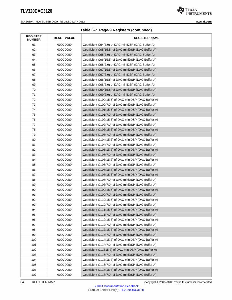
TLV320DAC3120
SLAS659A –NOVEMBER 2009–REVISED MAY 2012 www.ti.com
Table 6-7. Page-9 Registers (continued)
REGISTER RESET VALUE REGISTER NAMENUMBER
61 0000 0000 Coefficient C94(7:0) of DAC miniDSP (DAC Buffer A)
62 0000 0000 Coefficient C95(15:8) of DAC miniDSP (DAC Buffer A)
63 0000 0000 Coefficient C95(7:0) of DAC miniDSP (DAC Buffer A)
64 0000 0000 Coefficient C96(15:8) of DAC miniDSP (DAC Buffer A)
65 0000 0000 Coefficient C96(7:0) of DAC miniDSP (DAC Buffer A)
66 0000 0000 Coefficient C97(15:8) of DAC miniDSP (DAC Buffer A)
67 0000 0000 Coefficient C97(7:0) of DAC miniDSP (DAC Buffer A)
68 0000 0000 Coefficient C98(15:8) of DAC miniDSP (DAC Buffer A)
69 0000 0000 Coefficient C98(7:0) of DAC miniDSP (DAC Buffer A)
70 0000 0000 Coefficient C99(15:8) of DAC miniDSP (DAC Buffer A)
71 0000 0000 Coefficient C99(7:0) of DAC miniDSP (DAC Buffer A)
72 0000 0000 Coefficient C100(15:8) of DAC miniDSP (DAC Buffer A)
73 0000 0000 Coefficient C100(7:0) of DAC miniDSP (DAC Buffer A)
74 0000 0000 Coefficient C101(15:8) of DAC miniDSP (DAC Buffer A)
75 0000 0000 Coefficient C101(7:0) of DAC miniDSP (DAC Buffer A)
76 0000 0000 Coefficient C102(15:8) of DAC miniDSP (DAC Buffer A)
77 0000 0000 Coefficient C102(7:0) of DAC miniDSP (DAC Buffer A)
78 0000 0000 Coefficient C103(15:8) of DAC miniDSP (DAC Buffer A)
79 0000 0000 Coefficient C103(7:0) of DAC miniDSP (DAC Buffer A)
80 0000 0000 Coefficient C104(15:8) of DAC miniDSP (DAC Buffer A)
81 0000 0000 Coefficient C104(7:0) of DAC miniDSP (DAC Buffer A)
82 0000 0000 Coefficient C105(15:8) of DAC miniDSP (DAC Buffer A)
83 0000 0000 Coefficient C105(7:0) of DAC miniDSP (DAC Buffer A)
84 0000 0000 Coefficient C106(15:8) of DAC miniDSP (DAC Buffer A)
85 0000 0000 Coefficient C106(7:0) of DAC miniDSP (DAC Buffer A)
86 0000 0000 Coefficient C107(15:8) of DAC miniDSP (DAC Buffer A)
87 0000 0000 Coefficient C107(15:8) of DAC miniDSP (DAC Buffer A)
88 0000 0000 Coefficient C108(7:0) of DAC miniDSP (DAC Buffer A)
89 0000 0000 Coefficient C108(7:0) of DAC miniDSP (DAC Buffer A)
90 0000 0000 Coefficient C109(15:8) of DAC miniDSP (DAC Buffer A)
91 0000 0000 Coefficient C109(7:0) of DAC miniDSP (DAC Buffer A)
92 0000 0000 Coefficient C110(15:8) of DAC miniDSP (DAC Buffer A)
93 0000 0000 Coefficient C110(7:0) of DAC miniDSP (DAC Buffer A)
94 0000 0000 Coefficient C111(15:8) of DAC miniDSP (DAC Buffer A)
95 0000 0000 Coefficient C111(7:0) of DAC miniDSP (DAC Buffer A)
96 0000 0000 Coefficient C112(15:8) of DAC miniDSP (DAC Buffer A)
97 0000 0000 Coefficient C112(7:0) of DAC miniDSP (DAC Buffer A)
98 0000 0000 Coefficient C113(15:8) of DAC miniDSP (DAC Buffer A)
99 0000 0000 Coefficient C113(7:0) of DAC miniDSP (DAC Buffer A)
100 0000 0000 Coefficient C114(15:8) of DAC miniDSP (DAC Buffer A)
101 0000 0000 Coefficient C114(7:0) of DAC miniDSP (DAC Buffer A)
102 0000 0000 Coefficient C11515:8) of DAC miniDSP (DAC Buffer A)
103 0000 0000 Coefficient C115(7:0) of DAC miniDSP (DAC Buffer A)
104 0000 0000 Coefficient C116(15:8) of DAC miniDSP (DAC Buffer A)
105 0000 0000 Coefficient C116(7:0) of DAC miniDSP (DAC Buffer A)
106 0000 0000 Coefficient C117(15:8) of DAC miniDSP (DAC Buffer A)
107 0000 0000 Coefficient C117(7:0) of DAC miniDSP (DAC Buffer A)
84 REGISTER MAP Copyright © 2009–2012, Texas Instruments Incorporated
Submit Documentation FeedbackProduct Folder Link(s): TLV320DAC3120
TLV320DAC3120
www.ti.com SLAS659A –NOVEMBER 2009–REVISED MAY 2012
Table 6-7. Page-9 Registers (continued)
REGISTER RESET VALUE REGISTER NAMENUMBER
108 0000 0000 Coefficient C118(15:8) of DAC miniDSP (DAC Buffer A)
109 0000 0000 Coefficient C118(7:0) of DAC miniDSP (DAC Buffer A)
110 0000 0000 Coefficient C119(15:8) of DAC miniDSP (DAC Buffer A)
111 0000 0000 Coefficient C119(7:0) of DAC miniDSP (DAC Buffer A)
112 0000 0000 Coefficient C120(15:8) of DAC miniDSP (DAC Buffer A)
113 0000 0000 Coefficient C120(7:0) of DAC miniDSP (DAC Buffer A)
114 0000 0000 Coefficient C121(15:8) of DAC miniDSP (DAC Buffer A)
115 0000 0000 Coefficient C121(7:0) of DAC miniDSP (DAC Buffer A)
116 0000 0000 Coefficient C122(15:8) of DAC miniDSP (DAC Buffer A)
117 0000 0000 Coefficient C122(7:0) of DAC miniDSP (DAC Buffer A)
118 0000 0000 Coefficient C123(15:8) of DAC miniDSP (DAC Buffer A)
119 0000 0000 Coefficient C123(7:0) of DAC miniDSP (DAC Buffer A)
120 0000 0000 Coefficient C124(15:8) of DAC miniDSP (DAC Buffer A)
121 0000 0000 Coefficient C124(7:0) of DAC miniDSP (DAC Buffer A)
122 0000 0000 Coefficient C125(15:8) of DAC miniDSP (DAC Buffer A)
123 0000 0000 Coefficient C125(7:0) of DAC miniDSP (DAC Buffer A)
124 0000 0000 Coefficient C126(15:8) of DAC miniDSP (DAC Buffer A)
125 0000 0000 Coefficient C126(7:0) of DAC miniDSP (DAC Buffer A)
126 0000 0000 Coefficient C127(15:8) of DAC miniDSP (DAC Buffer A)
127 0000 0000 Coefficient C127(7:0) of DAC miniDSP (DAC Buffer A)
6.7 Control Registers, Page 10: DAC Programmable Coefficients RAM Buffer A (129:191)
Table 6-8. Page-10 Registers
REGISTER RESET VALUE REGISTER NAMENUMBER
1 XXXX XXXX Reserved. Do not write to this register.
2 0000 0000 Coefficient C129(15:8) of DAC miniDSP (DAC Buffer A)
3 0000 0000 Coefficient C129(7:0) of DAC miniDSP (DAC Buffer A)
4 0000 0000 Coefficient C130(15:8) of DAC miniDSP (DAC Buffer A)
5 0000 0000 Coefficient C130(7:0) of DAC miniDSP (DAC Buffer A)
6 0000 0000 Coefficient C131(15:8) of DAC miniDSP (DAC Buffer A)
7 0000 0000 Coefficient C131(7:0) of DAC miniDSP (DAC Buffer A)
8 0000 0000 Coefficient C132(15:8) of DAC miniDSP (DAC Buffer A)
9 0000 0000 Coefficient C132(7:0) of DAC miniDSP (DAC Buffer A)
10 0000 0000 Coefficient C133(15:8) of DAC miniDSP (DAC Buffer A)
11 0000 0000 Coefficient C133(7:0) of DAC miniDSP (DAC Buffer A)
12 0000 0000 Coefficient C134(15:8) of DAC miniDSP (DAC Buffer A)
13 0000 0000 Coefficient C134(7:0) of DAC miniDSP (DAC Buffer A)
14 0000 0000 Coefficient C135(15:8) of DAC miniDSP (DAC Buffer A)
15 0000 0000 Coefficient C135(7:0) of DAC miniDSP (DAC Buffer A)
16 0000 0000 Coefficient C136(15:8) of DAC miniDSP (DAC Buffer A)
17 0000 0000 Coefficient C136(7:0) of DAC miniDSP (DAC Buffer A)
18 0000 0000 Coefficient C137(15:8) of DAC miniDSP (DAC Buffer A)
19 0000 0000 Coefficient C137(7:0) of DAC miniDSP (DAC Buffer A)
Copyright © 2009–2012, Texas Instruments Incorporated REGISTER MAP 85Submit Documentation Feedback
Product Folder Link(s): TLV320DAC3120

TLV320DAC3120
SLAS659A –NOVEMBER 2009–REVISED MAY 2012 www.ti.com
Table 6-8. Page-10 Registers (continued)
REGISTER RESET VALUE REGISTER NAMENUMBER
20 0000 0000 Coefficient C138(15:8) of DAC miniDSP (DAC Buffer A)
21 0000 0000 Coefficient C138(7:0) of DAC miniDSP (DAC Buffer A)
22 0000 0000 Coefficient C139(15:8) of DAC miniDSP (DAC Buffer A)
23 0000 0000 Coefficient C139(7:0) of DAC miniDSP (DAC Buffer A)
24 0000 0000 Coefficient C140(15:8) of DAC miniDSP (DAC Buffer A)
25 0000 0000 Coefficient C140(7:0) of DAC miniDSP (DAC Buffer A)
26 0000 0000 Coefficient C141(15:8) of DAC miniDSP (DAC Buffer A)
27 0000 0000 Coefficient C141(7:0) of DAC miniDSP (DAC Buffer A)
28 0000 0000 Coefficient C142(15:8) of DAC miniDSP (DAC Buffer A)
29 0000 0000 Coefficient C142(7:0) of DAC miniDSP (DAC Buffer A)
30 0000 0000 Coefficient C143(15:8) of DAC miniDSP (DAC Buffer A)
31 0000 0000 Coefficient C143(7:0) of DAC miniDSP (DAC Buffer A)
32 0000 0000 Coefficient C144(15:8) of DAC miniDSP (DAC Buffer A)
33 0000 0000 Coefficient C144(7:0) of DAC miniDSP (DAC Buffer A)
34 0000 0000 Coefficient C145(15:8) of DAC miniDSP (DAC Buffer A)
35 0000 0000 Coefficient C145(7:0) of DAC miniDSP (DAC Buffer A)
36 0000 0000 Coefficient C146(15:8) of DAC miniDSP (DAC Buffer A)
37 0000 0000 Coefficient C146(7:0) of DAC miniDSP (DAC Buffer A)
38 0000 0000 Coefficient C147(15:8) of DAC miniDSP (DAC Buffer A)
39 0000 0000 Coefficient C147(7:0) of DAC miniDSP (DAC Buffer A)
40 0000 0000 Coefficient C148(15:8) of DAC miniDSP (DAC Buffer A)
41 0000 0000 Coefficient C148(7:0) of DAC miniDSP (DAC Buffer A)
42 0000 0000 Coefficient C149(15:8) of DAC miniDSP (DAC Buffer A)
43 0000 0000 Coefficient C149(7:0) of DAC miniDSP (DAC Buffer A)
44 0000 0000 Coefficient C150(15:8) of DAC miniDSP (DAC Buffer A)
45 0000 0000 Coefficient C150(7:0) of DAC miniDSP (DAC Buffer A)
46 0000 0000 Coefficient C151(15:8) of DAC miniDSP (DAC Buffer A)
47 0000 0000 Coefficient C151(7:0) of DAC miniDSP (DAC Buffer A)
48 0000 0000 Coefficient C152(15:8) of DAC miniDSP (DAC Buffer A)
49 0000 0000 Coefficient C152(7:0) of DAC miniDSP (DAC Buffer A)
50 0000 0000 Coefficient C153(15:8) of DAC miniDSP (DAC Buffer A)
51 0000 0000 Coefficient C153(7:0) of DAC miniDSP (DAC Buffer A)
52 0000 0000 Coefficient C154(15:8) of DAC miniDSP (DAC Buffer A)
53 0000 0000 Coefficient C154(7:0) of DAC miniDSP (DAC Buffer A)
54 0000 0000 Coefficient C155(15:8) of DAC miniDSP (DAC Buffer A)
55 0000 0000 Coefficient C155(7:0) of DAC miniDSP (DAC Buffer A)
56 0000 0000 Coefficient C156(15:8) of DAC miniDSP (DAC Buffer A)
57 0000 0000 Coefficient C156(7:0) of DAC miniDSP (DAC Buffer A)
58 0000 0000 Coefficient C157(15:8) of DAC miniDSP (DAC Buffer A)
59 0000 0000 Coefficient C157(7:0) of DAC miniDSP (DAC Buffer A)
60 0000 0000 Coefficient C158(15:8) of DAC miniDSP (DAC Buffer A)
61 0000 0000 Coefficient C158(7:0) of DAC miniDSP (DAC Buffer A)
62 0000 0000 Coefficient C159(15:8) of DAC miniDSP (DAC Buffer A)
63 0000 0000 Coefficient C159(7:0) of DAC miniDSP (DAC Buffer A)
64 0000 0000 Coefficient C160(15:8) of DAC miniDSP (DAC Buffer A)
65 0000 0000 Coefficient C160(7:0) of DAC miniDSP (DAC Buffer A)
66 0000 0000 Coefficient C161(15:8) of DAC miniDSP (DAC Buffer A)
86 REGISTER MAP Copyright © 2009–2012, Texas Instruments Incorporated
Submit Documentation FeedbackProduct Folder Link(s): TLV320DAC3120

TLV320DAC3120
www.ti.com SLAS659A –NOVEMBER 2009–REVISED MAY 2012
Table 6-8. Page-10 Registers (continued)
REGISTER RESET VALUE REGISTER NAMENUMBER
67 0000 0000 Coefficient C161(7:0) of DAC miniDSP (DAC Buffer A)
68 0000 0000 Coefficient C162(15:8) of DAC miniDSP (DAC Buffer A)
69 0000 0000 Coefficient C162(7:0) of DAC miniDSP (DAC Buffer A)
70 0000 0000 Coefficient C163(15:8) of DAC miniDSP (DAC Buffer A)
71 0000 0000 Coefficient C163(7:0) of DAC miniDSP (DAC Buffer A)
72 0000 0000 Coefficient C164(15:8) of DAC miniDSP (DAC Buffer A)
73 0000 0000 Coefficient C164(7:0) of DAC miniDSP (DAC Buffer A)
74 0000 0000 Coefficient C165(15:8) of DAC miniDSP (DAC Buffer A)
75 0000 0000 Coefficient C165(7:0) of DAC miniDSP (DAC Buffer A)
76 0000 0000 Coefficient C166(15:8) of DAC miniDSP (DAC Buffer A)
77 0000 0000 Coefficient C166(7:0) of DAC miniDSP (DAC Buffer A)
78 0000 0000 Coefficient C167(15:8) of DAC miniDSP (DAC Buffer A)
79 0000 0000 Coefficient C167(7:0) of DAC miniDSP (DAC Buffer A)
80 0000 0000 Coefficient C168(15:8) of DAC miniDSP (DAC Buffer A)
81 0000 0000 Coefficient C168(7:0) of DAC miniDSP (DAC Buffer A)
82 0000 0000 Coefficient C169(15:8) of DAC miniDSP (DAC Buffer A)
83 0000 0000 Coefficient C169(7:0) of DAC miniDSP (DAC Buffer A)
84 0000 0000 Coefficient C170(15:8) of DAC miniDSP (DAC Buffer A)
85 0000 0000 Coefficient C170(7:0) of DAC miniDSP (DAC Buffer A)
86 0000 0000 Coefficient C171(15:8) of DAC miniDSP (DAC Buffer A)
87 0000 0000 Coefficient C171(7:0) of DAC miniDSP (DAC Buffer A)
88 0000 0000 Coefficient C172(15:8) of DAC miniDSP (DAC Buffer A)
89 0000 0000 Coefficient C172(7:0) of DAC miniDSP (DAC Buffer A)
90 0000 0000 Coefficient C173(15:8) of DAC miniDSP (DAC Buffer A)
91 0000 0000 Coefficient C173(7:0) of DAC miniDSP (DAC Buffer A)
92 0000 0000 Coefficient C174(15:8) of DAC miniDSP (DAC Buffer A)
93 0000 0000 Coefficient C174(7:0) of DAC miniDSP (DAC Buffer A)
94 0000 0000 Coefficient C175(15:8) of DAC miniDSP (DAC Buffer A)
95 0000 0000 Coefficient C175(7:0) of DAC miniDSP (DAC Buffer A)
96 0000 0000 Coefficient C176(15:8) of DAC miniDSP (DAC Buffer A)
97 0000 0000 Coefficient C176(7:0) of DAC miniDSP (DAC Buffer A)
98 0000 0000 Coefficient C177(15:8) of DAC miniDSP (DAC Buffer A)
99 0000 0000 Coefficient C177(7:0) of DAC miniDSP (DAC Buffer A)
100 0000 0000 Coefficient C178(15:8) of DAC miniDSP (DAC Buffer A)
101 0000 0000 Coefficient C178(7:0) of DAC miniDSP (DAC Buffer A)
102 0000 0000 Coefficient C179(15:8) of DAC miniDSP (DAC Buffer A)
103 0000 0000 Coefficient C179(7:0) of DAC miniDSP (DAC Buffer A)
104 0000 0000 Coefficient C180(15:8) of DAC miniDSP (DAC Buffer A)
105 0000 0000 Coefficient C180(7:0) of DAC miniDSP (DAC Buffer A)
106 0000 0000 Coefficient C181(15:8) of DAC miniDSP (DAC Buffer A)
107 0000 0000 Coefficient C181(7:0) of DAC miniDSP (DAC Buffer A)
108 0000 0000 Coefficient C182(15:8) of DAC miniDSP (DAC Buffer A)
109 0000 0000 Coefficient C182(7:0) of DAC miniDSP (DAC Buffer A)
110 0000 0000 Coefficient C183(15:8) of DAC miniDSP (DAC Buffer A)
111 0000 0000 Coefficient C183(7:0) of DAC miniDSP (DAC Buffer A)
112 0000 0000 Coefficient C184(15:8) of DAC miniDSP (DAC Buffer A)
113 0000 0000 Coefficient C184(7:0) of DAC miniDSP (DAC Buffer A)
Copyright © 2009–2012, Texas Instruments Incorporated REGISTER MAP 87Submit Documentation Feedback
Product Folder Link(s): TLV320DAC3120
TLV320DAC3120
SLAS659A –NOVEMBER 2009–REVISED MAY 2012 www.ti.com
Table 6-8. Page-10 Registers (continued)
REGISTER RESET VALUE REGISTER NAMENUMBER
114 0000 0000 Coefficient C185(15:8) of DAC miniDSP (DAC Buffer A)
115 0000 0000 Coefficient C185(7:0) of DAC miniDSP (DAC Buffer A)
116 0000 0000 Coefficient C186(15:8) of DAC miniDSP (DAC Buffer A)
117 0000 0000 Coefficient C186(7:0) of DAC miniDSP (DAC Buffer A)
118 0000 0000 Coefficient C187(15:8) of DAC miniDSP (DAC Buffer A)
119 0000 0000 Coefficient C187(7:0) of DAC miniDSP (DAC Buffer A)
120 0000 0000 Coefficient C188(15:8) of DAC miniDSP (DAC Buffer A)
121 0000 0000 Coefficient C188(7:0) of DAC miniDSP (DAC Buffer A)
122 0000 0000 Coefficient C189(15:8) of DAC miniDSP (DAC Buffer A)
123 0000 0000 Coefficient C189(7:0) of DAC miniDSP (DAC Buffer A)
124 0000 0000 Coefficient C190(15:8) of DAC miniDSP (DAC Buffer A)
125 0000 0000 Coefficient C190(7:0) of DAC miniDSP (DAC Buffer A)
126 0000 0000 Coefficient C191(15:8) of DAC miniDSP (DAC Buffer A)
127 0000 0000 Coefficient C191(7:0) of DAC miniDSP (DAC Buffer A)
6.8 Control Registers, Page 11: DAC Programmable Coefficients RAM Buffer A (193:255)
Table 6-9. Page-11 Registers
REGISTER RESET VALUE REGISTER NAMENUMBER
1 XXXX XXXX Reserved. Do not write to this register.
2 0000 0000 Coefficient C193(15:8) of DAC miniDSP (DAC Buffer A)
3 0000 0000 Coefficient C193(7:0) of DAC miniDSP (DAC Buffer A)
4 0000 0000 Coefficient C194(15:8) of DAC miniDSP (DAC Buffer A)
5 0000 0000 Coefficient C194(7:0) of DAC miniDSP (DAC Buffer A)
6 0000 0000 Coefficient C195(15:8) of DAC miniDSP (DAC Buffer A)
7 0000 0000 Coefficient C195(7:0) of DAC miniDSP (DAC Buffer A)
8 0000 0000 Coefficient C196(15:8) of DAC miniDSP (DAC Buffer A)
9 0000 0000 Coefficient C196(7:0) of DAC miniDSP (DAC Buffer A)
10 0000 0000 Coefficient C197(15:8) of DAC miniDSP (DAC Buffer A)
11 0000 0000 Coefficient C197(7:0) of DAC miniDSP (DAC Buffer A)
12 0000 0000 Coefficient C198(15:8) of DAC miniDSP (DAC Buffer A)
13 0000 0000 Coefficient C198(7:0) of DAC miniDSP (DAC Buffer A)
14 0000 0000 Coefficient C199(15:8) of DAC miniDSP (DAC Buffer A)
15 0000 0000 Coefficient C199(7:0) of DAC miniDSP (DAC Buffer A)
16 0000 0000 Coefficient C200(15:8) of DAC miniDSP (DAC Buffer A)
17 0000 0000 Coefficient C200(7:0) of DAC miniDSP (DAC Buffer A)
18 0000 0000 Coefficient C201(15:8) of DAC miniDSP (DAC Buffer A)
19 0000 0000 Coefficient C201(7:0) of DAC miniDSP (DAC Buffer A)
20 0000 0000 Coefficient C202(15:8) of DAC miniDSP (DAC Buffer A)
21 0000 0000 Coefficient C202(7:0) of DAC miniDSP (DAC Buffer A)
22 0000 0000 Coefficient C203(15:8) of DAC miniDSP (DAC Buffer A)
23 0000 0000 Coefficient C203(7:0) of DAC miniDSP (DAC Buffer A)
24 0000 0000 Coefficient C204(15:8) of DAC miniDSP (DAC Buffer A)
25 0000 0000 Coefficient C204(7:0) of DAC miniDSP (DAC Buffer A)
88 REGISTER MAP Copyright © 2009–2012, Texas Instruments Incorporated
Submit Documentation FeedbackProduct Folder Link(s): TLV320DAC3120
TLV320DAC3120
www.ti.com SLAS659A –NOVEMBER 2009–REVISED MAY 2012
Table 6-9. Page-11 Registers (continued)
REGISTER RESET VALUE REGISTER NAMENUMBER
26 0000 0000 Coefficient C205(15:8) of DAC miniDSP (DAC Buffer A)
27 0000 0000 Coefficient C205(7:0) of DAC miniDSP (DAC Buffer A)
28 0000 0000 Coefficient C206(15:8) of DAC miniDSP (DAC Buffer A)
29 0000 0000 Coefficient C206(7:0) of DAC miniDSP (DAC Buffer A)
30 0000 0000 Coefficient C207(15:8) of DAC miniDSP (DAC Buffer A)
31 0000 0000 Coefficient C207(7:0) of DAC miniDSP (DAC Buffer A)
32 0000 0000 Coefficient C208(15:8) of DAC miniDSP (DAC Buffer A)
33 0000 0000 Coefficient C208(7:0) of DAC miniDSP (DAC Buffer A)
34 0000 0000 Coefficient C209(15:8) of DAC miniDSP (DAC Buffer A)
35 0000 0000 Coefficient C209(7:0) of DAC miniDSP (DAC Buffer A)
36 0000 0000 Coefficient C210(15:8) of DAC miniDSP (DAC Buffer A)
37 0000 0000 Coefficient C210(7:0) of DAC miniDSP (DAC Buffer A)
38 0000 0000 Coefficient C211(15:8) of DAC miniDSP (DAC Buffer A)
39 0000 0000 Coefficient C211(7:0) of DAC miniDSP (DAC Buffer A)
40 0000 0000 Coefficient C212(15:8) of DAC miniDSP (DAC Buffer A)
41 0000 0000 Coefficient C212(7:0) of DAC miniDSP (DAC Buffer A)
42 0000 0000 Coefficient C213(15:8) of DAC miniDSP (DAC Buffer A)
43 0000 0000 Coefficient C213(7:0) of DAC miniDSP (DAC Buffer A)
44 0000 0000 Coefficient C214(15:8) of DAC miniDSP (DAC Buffer A)
45 0000 0000 Coefficient C214(7:0) of DAC miniDSP (DAC Buffer A)
46 0000 0000 Coefficient C215(15:8) of DAC miniDSP (DAC Buffer A)
47 0000 0000 Coefficient C215(7:0) of DAC miniDSP (DAC Buffer A)
48 0000 0000 Coefficient C216(15:8) of DAC miniDSP (DAC Buffer A)
49 0000 0000 Coefficient C216(7:0) of DAC miniDSP (DAC Buffer A)
50 0000 0000 Coefficient C217(15:8) of DAC miniDSP (DAC Buffer A)
51 0000 0000 Coefficient C217(7:0) of DAC miniDSP (DAC Buffer A)
52 0000 0000 Coefficient C218(15:8) of DAC miniDSP (DAC Buffer A)
53 0000 0000 Coefficient C218(7:0) of DAC miniDSP (DAC Buffer A)
54 0000 0000 Coefficient C219(15:8) of DAC miniDSP (DAC Buffer A)
55 0000 0000 Coefficient C219(7:0) of DAC miniDSP (DAC Buffer A)
56 0000 0000 Coefficient C220(15:8) of DAC miniDSP (DAC Buffer A)
57 0000 0000 Coefficient C220(7:0) of DAC miniDSP (DAC Buffer A)
58 0000 0000 Coefficient C221(15:8) of DAC miniDSP (DAC Buffer A)
59 0000 0000 Coefficient C221(7:0) of DAC miniDSP (DAC Buffer A)
60 0000 0000 Coefficient C222(15:8) of DAC miniDSP (DAC Buffer A)
61 0000 0000 Coefficient C222(7:0) of DAC miniDSP (DAC Buffer A)
62 0000 0000 Coefficient C223(15:8) of DAC miniDSP (DAC Buffer A)
63 0000 0000 Coefficient C223(7:0) of DAC miniDSP (DAC Buffer A)
64 0000 0000 Coefficient C224(15:8) of DAC miniDSP (DAC Buffer A)
65 0000 0000 Coefficient C224(7:0) of DAC miniDSP (DAC Buffer A)
66 0000 0000 Coefficient C225(15:8) of DAC miniDSP (DAC Buffer A)
67 0000 0000 Coefficient C225(7:0) of DAC miniDSP (DAC Buffer A)
68 0000 0000 Coefficient C226(15:8) of DAC miniDSP (DAC Buffer A)
69 0000 0000 Coefficient C226(7:0) of DAC miniDSP (DAC Buffer A)
70 0000 0000 Coefficient C227(15:8) of DAC miniDSP (DAC Buffer A)
71 0000 0000 Coefficient C227(7:0) of DAC miniDSP (DAC Buffer A)
72 0000 0000 Coefficient C228(15:8) of DAC miniDSP (DAC Buffer A)
Copyright © 2009–2012, Texas Instruments Incorporated REGISTER MAP 89Submit Documentation Feedback
Product Folder Link(s): TLV320DAC3120
TLV320DAC3120
SLAS659A –NOVEMBER 2009–REVISED MAY 2012 www.ti.com
Table 6-9. Page-11 Registers (continued)
REGISTER RESET VALUE REGISTER NAMENUMBER
73 0000 0000 Coefficient C228(7:0) of DAC miniDSP (DAC Buffer A)
74 0000 0000 Coefficient C229(15:8) of DAC miniDSP (DAC Buffer A)
75 0000 0000 Coefficient C229(7:0) of DAC miniDSP (DAC Buffer A)
76 0000 0000 Coefficient C230(15:8) of DAC miniDSP (DAC Buffer A)
77 0000 0000 Coefficient C230(7:0) of DAC miniDSP (DAC Buffer A)
78 0000 0000 Coefficient C231(15:8) of DAC miniDSP (DAC Buffer A)
79 0000 0000 Coefficient C231(7:0) of DAC miniDSP (DAC Buffer A)
80 0000 0000 Coefficient C232(15:8) of DAC miniDSP (DAC Buffer A)
81 0000 0000 Coefficient C232(7:0) of DAC miniDSP (DAC Buffer A)
82 0000 0000 Coefficient C233(15:8) of DAC miniDSP (DAC Buffer A)
83 0000 0000 Coefficient C233(7:0) of DAC miniDSP (DAC Buffer A)
84 0000 0000 Coefficient C234(15:8) of DAC miniDSP (DAC Buffer A)
85 0000 0000 Coefficient C234(7:0) of DAC miniDSP (DAC Buffer A)
86 0000 0000 Coefficient C235(15:8) of DAC miniDSP (DAC Buffer A)
87 0000 0000 Coefficient C235(7:0) of DAC miniDSP (DAC Buffer A)
88 0000 0000 Coefficient C236(15:8) of DAC miniDSP (DAC Buffer A)
89 0000 0000 Coefficient C236(7:0) of DAC miniDSP (DAC Buffer A)
90 0000 0000 Coefficient C237(15:8) of DAC miniDSP (DAC Buffer A)
91 0000 0000 Coefficient C237(7:0) of DAC miniDSP (DAC Buffer A)
92 0000 0000 Coefficient C238(15:8) of DAC miniDSP (DAC Buffer A)
93 0000 0000 Coefficient C238(7:0) of DAC miniDSP (DAC Buffer A)
94 0000 0000 Coefficient C239(15:8) of DAC miniDSP (DAC Buffer A)
95 0000 0000 Coefficient C239(7:0) of DAC miniDSP (DAC Buffer A)
96 0000 0000 Coefficient C240(15:8) of DAC miniDSP (DAC Buffer A)
97 0000 0000 Coefficient C240(7:0) of DAC miniDSP (DAC Buffer A)
98 0000 0000 Coefficient C241(15:8) of DAC miniDSP (DAC Buffer A)
99 0000 0000 Coefficient C241(7:0) of DAC miniDSP (DAC Buffer A)
100 0000 0000 Coefficient C242(15:8) of DAC miniDSP (DAC Buffer A)
101 0000 0000 Coefficient C242(7:0) of DAC miniDSP (DAC Buffer A)
102 0000 0000 Coefficient C243(15:8) of DAC miniDSP (DAC Buffer A)
103 0000 0000 Coefficient C243(7:0) of DAC miniDSP (DAC Buffer A)
104 0000 0000 Coefficient C244(15:8) of DAC miniDSP (DAC Buffer A)
105 0000 0000 Coefficient C244(7:0) of DAC miniDSP (DAC Buffer A)
106 0000 0000 Coefficient C245(15:8) of DAC miniDSP (DAC Buffer A)
107 0000 0000 Coefficient C245(7:0) of DAC miniDSP (DAC Buffer A)
108 0000 0000 Coefficient C246(15:8) of DAC miniDSP (DAC Buffer A)
109 0000 0000 Coefficient C246(7:0) of DAC miniDSP (DAC Buffer A)
110 0000 0000 Coefficient C247(15:8) of DAC miniDSP (DAC Buffer A)
111 0000 0000 Coefficient C247(7:0) of DAC miniDSP (DAC Buffer A)
112 0000 0000 Coefficient C248(15:8) of DAC miniDSP (DAC Buffer A)
113 0000 0000 Coefficient C248(7:0) of DAC miniDSP (DAC Buffer A)
114 0000 0000 Coefficient C249(15:8) of DAC miniDSP (DAC Buffer A)
115 0000 0000 Coefficient C249(7:0) of DAC miniDSP (DAC Buffer A)
116 0000 0000 Coefficient C250(15:8) of DAC miniDSP (DAC Buffer A)
117 0000 0000 Coefficient C250(7:0) of DAC miniDSP (DAC Buffer A)
118 0000 0000 Coefficient C251(15:8) of DAC miniDSP (DAC Buffer A)
119 0000 0000 Coefficient C251(7:0) of DAC miniDSP (DAC Buffer A)
90 REGISTER MAP Copyright © 2009–2012, Texas Instruments Incorporated
Submit Documentation FeedbackProduct Folder Link(s): TLV320DAC3120
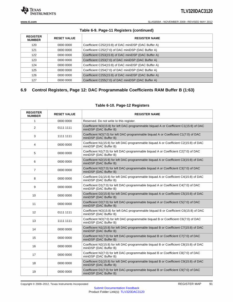
TLV320DAC3120
www.ti.com SLAS659A –NOVEMBER 2009–REVISED MAY 2012
Table 6-9. Page-11 Registers (continued)
REGISTER RESET VALUE REGISTER NAMENUMBER
120 0000 0000 Coefficient C252(15:8) of DAC miniDSP (DAC Buffer A)
121 0000 0000 Coefficient C252(7:0) of DAC miniDSP (DAC Buffer A)
122 0000 0000 Coefficient C253(15:8) of DAC miniDSP (DAC Buffer A)
123 0000 0000 Coefficient C253(7:0) of DAC miniDSP (DAC Buffer A)
124 0000 0000 Coefficient C254(15:8) of DAC miniDSP (DAC Buffer A)
125 0000 0000 Coefficient C254(7:0) of DAC miniDSP (DAC Buffer A)
126 0000 0000 Coefficient C255(15:8) of DAC miniDSP (DAC Buffer A)
127 0000 0000 Coefficient C255(7:0) of DAC miniDSP (DAC Buffer A)
6.9 Control Registers, Page 12: DAC Programmable Coefficients RAM Buffer B (1:63)
Table 6-10. Page-12 Registers
REGISTER RESET VALUE REGISTER NAMENUMBER
1 0000 0000 Reserved. Do not write to this register.
Coefficient NO(15:8) for left DAC-programmable biquad A or Coefficient C1(15:8) of DAC2 0111 1111 miniDSP (DAC Buffer B)
Coefficient NO(7:0) for left DAC-programmable biquad A or Coefficient C1(7:0) of DAC3 1111 1111 miniDSP (DAC Buffer B)
Coefficient N1(15:8) for left DAC-programmable biquad A or Coefficient C2(15:8) of DAC4 0000 0000 miniDSP (DAC Buffer B)
Coefficient N1(7:0) for left DAC-programmable biquad A or Coefficient C2(7:0) of DAC5 0000 0000 miniDSP (DAC Buffer B)
Coefficient N2(15:8) for left DAC-programmable biquad A or Coefficient C3(15:8) of DAC6 0000 0000 miniDSP (DAC Buffer B)
Coefficient N2(7:0) for left DAC-programmable biquad A or Coefficient C3(7:0) of DAC7 0000 0000 miniDSP (DAC Buffer B)
Coefficient D1(15:8) for left DAC-programmable biquad A or Coefficient C4(15:8) of DAC8 0000 0000 miniDSP (DAC Buffer B)
Coefficient D1(7:0) for left DAC-programmable biquad A or Coefficient C4(7:0) of DAC9 0000 0000 miniDSP (DAC Buffer B)
Coefficient D2(15:8) for left DAC-programmable biquad A or Coefficient C5(15:8) of DAC10 0000 0000 miniDSP (DAC Buffer B)
Coefficient D2(7:0) for left DAC-programmable biquad A or Coefficient C5(7:0) of DAC11 0000 0000 miniDSP (DAC Buffer B)
Coefficient NO(15:8) for left DAC-programmable biquad B or Coefficient C6(15:8) of DAC12 0111 1111 miniDSP (DAC Buffer B)
Coefficient NO(7:0) for left DAC-programmable biquad B or Coefficient C6(7:0) of DAC13 1111 1111 miniDSP (DAC Buffer B)
Coefficient N1(15:8) for left DAC-programmable biquad B or Coefficient C7(15:8) of DAC14 0000 0000 miniDSP (DAC Buffer B)
Coefficient N1(7:0) for left DAC-programmable biquad B or Coefficient C7(7:0) of DAC15 0000 0000 miniDSP (DAC Buffer B)
Coefficient N2(15:8) for left DAC-programmable biquad B or Coefficient C8(15:8) of DAC16 0000 0000 miniDSP (DAC Buffer B)
Coefficient N2(7:0) for left DAC-programmable biquad B or Coefficient C8(7:0) of DAC17 0000 0000 miniDSP (DAC Buffer B)
Coefficient D1(15:8) for left DAC-programmable biquad B or Coefficient C9(15:8) of DAC18 0000 0000 miniDSP (DAC Buffer B)
Coefficient D1(7:0) for left DAC-programmable biquad B or Coefficient C9(7:0) of DAC19 0000 0000 miniDSP (DAC Buffer B)
Copyright © 2009–2012, Texas Instruments Incorporated REGISTER MAP 91Submit Documentation Feedback
Product Folder Link(s): TLV320DAC3120
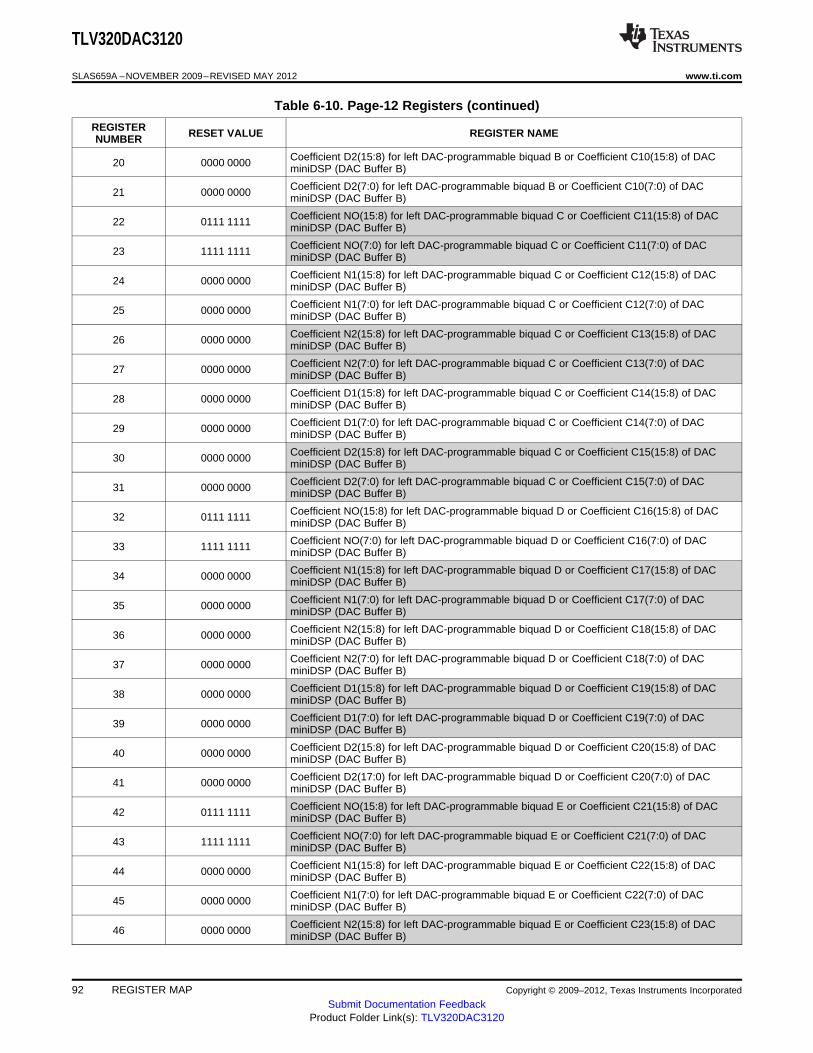
TLV320DAC3120
SLAS659A –NOVEMBER 2009–REVISED MAY 2012 www.ti.com
Table 6-10. Page-12 Registers (continued)
REGISTER RESET VALUE REGISTER NAMENUMBER
Coefficient D2(15:8) for left DAC-programmable biquad B or Coefficient C10(15:8) of DAC20 0000 0000 miniDSP (DAC Buffer B)
Coefficient D2(7:0) for left DAC-programmable biquad B or Coefficient C10(7:0) of DAC21 0000 0000 miniDSP (DAC Buffer B)
Coefficient NO(15:8) for left DAC-programmable biquad C or Coefficient C11(15:8) of DAC22 0111 1111 miniDSP (DAC Buffer B)
Coefficient NO(7:0) for left DAC-programmable biquad C or Coefficient C11(7:0) of DAC23 1111 1111 miniDSP (DAC Buffer B)
Coefficient N1(15:8) for left DAC-programmable biquad C or Coefficient C12(15:8) of DAC24 0000 0000 miniDSP (DAC Buffer B)
Coefficient N1(7:0) for left DAC-programmable biquad C or Coefficient C12(7:0) of DAC25 0000 0000 miniDSP (DAC Buffer B)
Coefficient N2(15:8) for left DAC-programmable biquad C or Coefficient C13(15:8) of DAC26 0000 0000 miniDSP (DAC Buffer B)
Coefficient N2(7:0) for left DAC-programmable biquad C or Coefficient C13(7:0) of DAC27 0000 0000 miniDSP (DAC Buffer B)
Coefficient D1(15:8) for left DAC-programmable biquad C or Coefficient C14(15:8) of DAC28 0000 0000 miniDSP (DAC Buffer B)
Coefficient D1(7:0) for left DAC-programmable biquad C or Coefficient C14(7:0) of DAC29 0000 0000 miniDSP (DAC Buffer B)
Coefficient D2(15:8) for left DAC-programmable biquad C or Coefficient C15(15:8) of DAC30 0000 0000 miniDSP (DAC Buffer B)
Coefficient D2(7:0) for left DAC-programmable biquad C or Coefficient C15(7:0) of DAC31 0000 0000 miniDSP (DAC Buffer B)
Coefficient NO(15:8) for left DAC-programmable biquad D or Coefficient C16(15:8) of DAC32 0111 1111 miniDSP (DAC Buffer B)
Coefficient NO(7:0) for left DAC-programmable biquad D or Coefficient C16(7:0) of DAC33 1111 1111 miniDSP (DAC Buffer B)
Coefficient N1(15:8) for left DAC-programmable biquad D or Coefficient C17(15:8) of DAC34 0000 0000 miniDSP (DAC Buffer B)
Coefficient N1(7:0) for left DAC-programmable biquad D or Coefficient C17(7:0) of DAC35 0000 0000 miniDSP (DAC Buffer B)
Coefficient N2(15:8) for left DAC-programmable biquad D or Coefficient C18(15:8) of DAC36 0000 0000 miniDSP (DAC Buffer B)
Coefficient N2(7:0) for left DAC-programmable biquad D or Coefficient C18(7:0) of DAC37 0000 0000 miniDSP (DAC Buffer B)
Coefficient D1(15:8) for left DAC-programmable biquad D or Coefficient C19(15:8) of DAC38 0000 0000 miniDSP (DAC Buffer B)
Coefficient D1(7:0) for left DAC-programmable biquad D or Coefficient C19(7:0) of DAC39 0000 0000 miniDSP (DAC Buffer B)
Coefficient D2(15:8) for left DAC-programmable biquad D or Coefficient C20(15:8) of DAC40 0000 0000 miniDSP (DAC Buffer B)
Coefficient D2(17:0) for left DAC-programmable biquad D or Coefficient C20(7:0) of DAC41 0000 0000 miniDSP (DAC Buffer B)
Coefficient NO(15:8) for left DAC-programmable biquad E or Coefficient C21(15:8) of DAC42 0111 1111 miniDSP (DAC Buffer B)
Coefficient NO(7:0) for left DAC-programmable biquad E or Coefficient C21(7:0) of DAC43 1111 1111 miniDSP (DAC Buffer B)
Coefficient N1(15:8) for left DAC-programmable biquad E or Coefficient C22(15:8) of DAC44 0000 0000 miniDSP (DAC Buffer B)
Coefficient N1(7:0) for left DAC-programmable biquad E or Coefficient C22(7:0) of DAC45 0000 0000 miniDSP (DAC Buffer B)
Coefficient N2(15:8) for left DAC-programmable biquad E or Coefficient C23(15:8) of DAC46 0000 0000 miniDSP (DAC Buffer B)
92 REGISTER MAP Copyright © 2009–2012, Texas Instruments Incorporated
Submit Documentation FeedbackProduct Folder Link(s): TLV320DAC3120
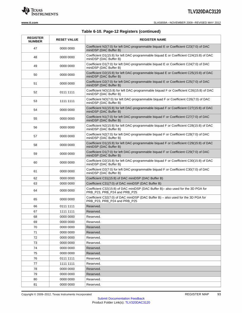
TLV320DAC3120
www.ti.com SLAS659A –NOVEMBER 2009–REVISED MAY 2012
Table 6-10. Page-12 Registers (continued)
REGISTER RESET VALUE REGISTER NAMENUMBER
Coefficient N2(7:0) for left DAC-programmable biquad E or Coefficient C23(7:0) of DAC47 0000 0000 miniDSP (DAC Buffer B)
Coefficient D1(15:8) for left DAC-programmable biquad E or Coefficient C24(15:8) of DAC48 0000 0000 miniDSP (DAC Buffer B)
Coefficient D1(7:0) for left DAC-programmable biquad E or Coefficient C24(7:0) of DAC49 0000 0000 miniDSP (DAC Buffer B)
Coefficient D2(15:8) for left DAC-programmable biquad E or Coefficient C25(15:8) of DAC50 0000 0000 miniDSP (DAC Buffer B)
Coefficient D2(7:0) for left DAC-programmable biquad E or Coefficient C25(7:0) of DAC51 0000 0000 miniDSP (DAC Buffer B)
Coefficient NO(15:8) for left DAC-programmable biquad F or Coefficient C26(15:8) of DAC52 0111 1111 miniDSP (DAC Buffer B)
Coefficient NO(7:0) for left DAC-programmable biquad F or Coefficient C26(7:0) of DAC53 1111 1111 miniDSP (DAC Buffer B)
Coefficient N1(15:8) for left DAC-programmable biquad F or Coefficient C27(15:8) of DAC54 0000 0000 miniDSP (DAC Buffer B)
Coefficient N1(7:0) for left DAC-programmable biquad F or Coefficient C27(7:0) of DAC55 0000 0000 miniDSP (DAC Buffer B)
Coefficient N2(15:8) for left DAC-programmable biquad F or Coefficient C28(15:8) of DAC56 0000 0000 miniDSP (DAC Buffer B)
Coefficient N2(7:0) for left DAC-programmable biquad F or Coefficient C28(7:0) of DAC57 0000 0000 miniDSP (DAC Buffer B)
Coefficient D1(15:8) for left DAC-programmable biquad F or Coefficient C29(15:8) of DAC58 0000 0000 miniDSP (DAC Buffer B)
Coefficient D1(7:0) for left DAC-programmable biquad F or Coefficient C29(7:0) of DAC59 0000 0000 miniDSP (DAC Buffer B)
Coefficient D2(15:8) for left DAC-programmable biquad F or Coefficient C30(15:8) of DAC60 0000 0000 miniDSP (DAC Buffer B)
Coefficient D2(7:0) for left DAC-programmable biquad F or Coefficient C30(7:0) of DAC61 0000 0000 miniDSP (DAC Buffer B)
62 0000 0000 Coefficient C31(15:8) of DAC miniDSP (DAC Buffer B)
63 0000 0000 Coefficient C31(7:0) of DAC miniDSP (DAC Buffer B)
Coefficient C32(15:8) of DAC miniDSP (DAC Buffer B)– also used for the 3D PGA for64 0000 0000 PRB_P23, PRB_P24 and PRB_P25
Coefficient C32(7:0) of DAC miniDSP (DAC Buffer B) – also used for the 3D PGA for65 0000 0000 PRB_P23, PRB_P24 and PRB_P25
66 0111 1111 Reserved.
67 1111 1111 Reserved.
68 0000 0000 Reserved.
69 0000 0000 Reserved.
70 0000 0000 Reserved.
71 0000 0000 Reserved.
72 0000 0000 Reserved.
73 0000 0000 Reserved.
74 0000 0000 Reserved.
75 0000 0000 Reserved.
76 0111 1111 Reserved.
77 1111 1111 Reserved.
78 0000 0000 Reserved.
79 0000 0000 Reserved.
80 0000 0000 Reserved.
81 0000 0000 Reserved.
Copyright © 2009–2012, Texas Instruments Incorporated REGISTER MAP 93Submit Documentation Feedback
Product Folder Link(s): TLV320DAC3120
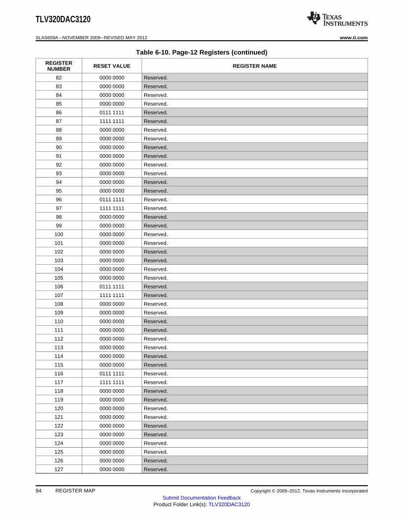
TLV320DAC3120
SLAS659A –NOVEMBER 2009–REVISED MAY 2012 www.ti.com
Table 6-10. Page-12 Registers (continued)
REGISTER RESET VALUE REGISTER NAMENUMBER
82 0000 0000 Reserved.
83 0000 0000 Reserved.
84 0000 0000 Reserved.
85 0000 0000 Reserved.
86 0111 1111 Reserved.
87 1111 1111 Reserved.
88 0000 0000 Reserved.
89 0000 0000 Reserved.
90 0000 0000 Reserved.
91 0000 0000 Reserved.
92 0000 0000 Reserved.
93 0000 0000 Reserved.
94 0000 0000 Reserved.
95 0000 0000 Reserved.
96 0111 1111 Reserved.
97 1111 1111 Reserved.
98 0000 0000 Reserved.
99 0000 0000 Reserved.
100 0000 0000 Reserved.
101 0000 0000 Reserved.
102 0000 0000 Reserved.
103 0000 0000 Reserved.
104 0000 0000 Reserved.
105 0000 0000 Reserved.
106 0111 1111 Reserved.
107 1111 1111 Reserved.
108 0000 0000 Reserved.
109 0000 0000 Reserved.
110 0000 0000 Reserved.
111 0000 0000 Reserved.
112 0000 0000 Reserved.
113 0000 0000 Reserved.
114 0000 0000 Reserved.
115 0000 0000 Reserved.
116 0111 1111 Reserved.
117 1111 1111 Reserved.
118 0000 0000 Reserved.
119 0000 0000 Reserved.
120 0000 0000 Reserved.
121 0000 0000 Reserved.
122 0000 0000 Reserved.
123 0000 0000 Reserved.
124 0000 0000 Reserved.
125 0000 0000 Reserved.
126 0000 0000 Reserved.
127 0000 0000 Reserved.
94 REGISTER MAP Copyright © 2009–2012, Texas Instruments Incorporated
Submit Documentation FeedbackProduct Folder Link(s): TLV320DAC3120
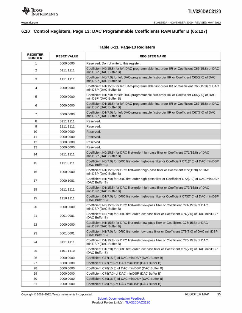
TLV320DAC3120
www.ti.com SLAS659A –NOVEMBER 2009–REVISED MAY 2012
6.10 Control Registers, Page 13: DAC Programmable Coefficients RAM Buffer B (65:127)
Table 6-11. Page-13 Registers
REGISTER RESET VALUE REGISTER NAMENUMBER
1 0000 0000 Reserved. Do not write to this register.
Coefficient N0(15:8) for left DAC-programmable first-order IIR or Coefficient C65(15:8) of DAC2 0111 1111 miniDSP (DAC Buffer B)
Coefficient N0(7:0) for left DAC-programmable first-order IIR or Coefficient C65(7:0) of DAC3 1111 1111 miniDSP (DAC Buffer B)
Coefficient N1(15:8) for left DAC-programmable first-order IIR or Coefficient C66(15:8) of DAC4 0000 0000 miniDSP (DAC Buffer B)
Coefficient N1(7:0) for left DAC-programmable first-order IIR or Coefficient C66(7:0) of DAC5 0000 0000 miniDSP (DAC Buffer B)
Coefficient D1(15:8) for left DAC-programmable first-order IIR or Coefficient C67(15:8) of DAC6 0000 0000 miniDSP (DAC Buffer B)
Coefficient D1(7:0) for left DAC-programmable first-order IIR or Coefficient C67(7:0) of DAC7 0000 0000 miniDSP (DAC Buffer B)
8 0111 1111 Reserved.
9 1111 1111 Reserved.
10 0000 0000 Reserved.
11 0000 0000 Reserved.
12 0000 0000 Reserved.
13 0000 0000 Reserved.
Coefficient N0(15:8) for DRC first-order high-pass filter or Coefficient C71(15:8) of DAC14 0111 1111 miniDSP (DAC Buffer B)
Coefficient N0(7:0) for DRC first-order high-pass filter or Coefficient C71(7:0) of DAC miniDSP15 1111 0111 (DAC Buffer B)
Coefficient N1(15:8) for DRC first-order high-pass filter or Coefficient C72(15:8) of DAC16 1000 0000 miniDSP (DAC Buffer B)
Coefficient N1(7:0) for DRC first-order high-pass filter or Coefficient C72(7:0) of DAC miniDSP17 0000 1001 (DAC Buffer B)
Coefficient D1(15:8) for DRC first-order high-pass filter or Coefficient C73(15:8) of DAC18 0111 1111 miniDSP (DAC Buffer B)
Coefficient D1(7:0) for DRC first-order high-pass filter or Coefficient C73(7:0) of DAC miniDSP19 1110 1111 (DAC Buffer B)
Coefficient N0(15:8) for DRC first-order low-pass filter or Coefficient C74(15:8) of DAC20 0000 0000 miniDSP (DAC Buffer B)
Coefficient N0(7:0) for DRC first-order low-pass filter or Coefficient C74(7:0) of DAC miniDSP21 0001 0001 (DAC Buffer B)
Coefficient N1(15:8) for DRC first-order low-pass filter or Coefficient C75(15:8) of DAC22 0000 0000 miniDSP (DAC Buffer B)
Coefficient N1(7:0) for DRC first-order low-pass filter or Coefficient C75(7:0) of DAC miniDSP23 0001 0001 (DAC Buffer B)
Coefficient D1(15:8) for DRC first-order low-pass filter or Coefficient C76(15:8) of DAC24 0111 1111 miniDSP (DAC Buffer B)
Coefficient D1(7:0) for DRC first-order low-pass filter or Coefficient C76(7:0) of DAC miniDSP25 1101 1110 (DAC Buffer B)
26 0000 0000 Coefficient C77(15:8) of DAC miniDSP (DAC Buffer B)
27 0000 0000 Coefficient C77(7:0) of DAC miniDSP (DAC Buffer B)
28 0000 0000 Coefficient C78(15:8) of DAC miniDSP (DAC Buffer B)
29 0000 0000 Coefficient C78(7:0) of DAC miniDSP (DAC Buffer B)
30 0000 0000 Coefficient C79(15:8) of DAC miniDSP (DAC Buffer B)
31 0000 0000 Coefficient C79(7:0) of DAC miniDSP (DAC Buffer B)
Copyright © 2009–2012, Texas Instruments Incorporated REGISTER MAP 95Submit Documentation Feedback
Product Folder Link(s): TLV320DAC3120
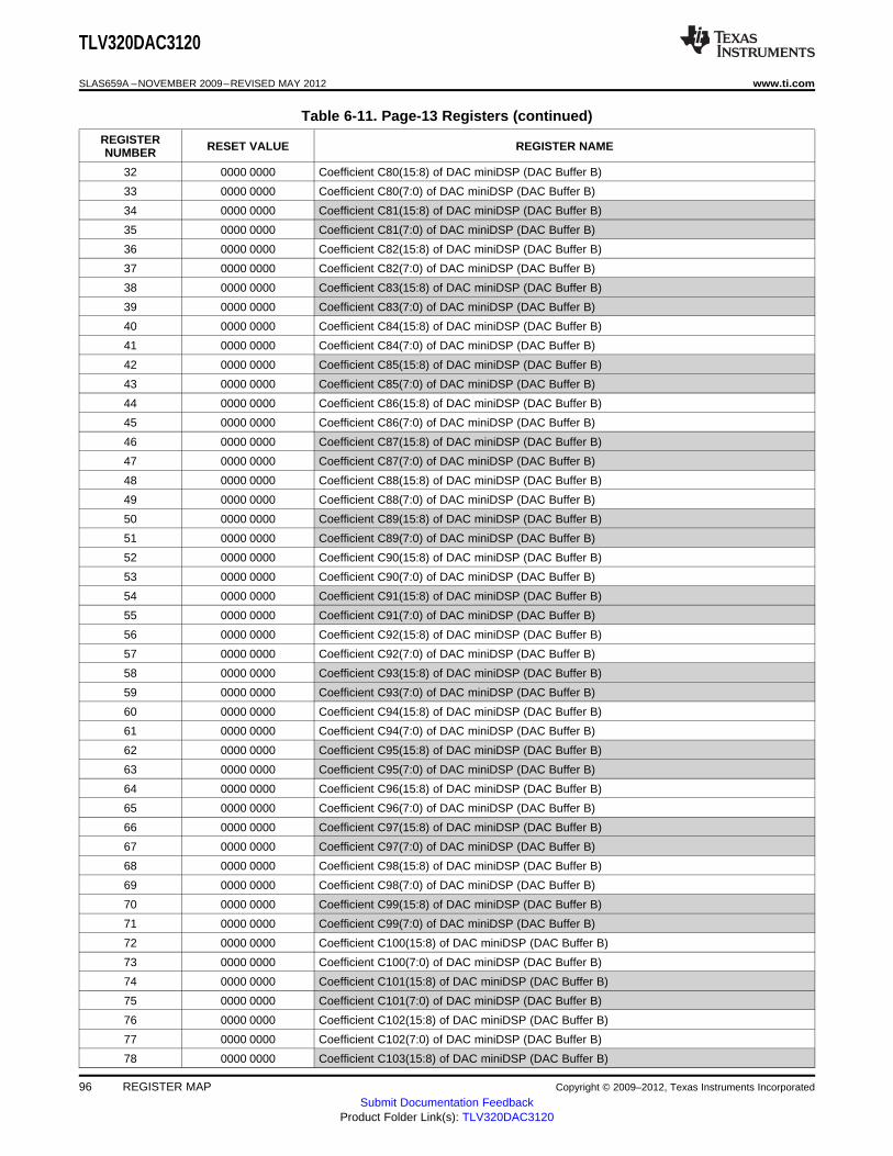
TLV320DAC3120
SLAS659A –NOVEMBER 2009–REVISED MAY 2012 www.ti.com
Table 6-11. Page-13 Registers (continued)
REGISTER RESET VALUE REGISTER NAMENUMBER
32 0000 0000 Coefficient C80(15:8) of DAC miniDSP (DAC Buffer B)
33 0000 0000 Coefficient C80(7:0) of DAC miniDSP (DAC Buffer B)
34 0000 0000 Coefficient C81(15:8) of DAC miniDSP (DAC Buffer B)
35 0000 0000 Coefficient C81(7:0) of DAC miniDSP (DAC Buffer B)
36 0000 0000 Coefficient C82(15:8) of DAC miniDSP (DAC Buffer B)
37 0000 0000 Coefficient C82(7:0) of DAC miniDSP (DAC Buffer B)
38 0000 0000 Coefficient C83(15:8) of DAC miniDSP (DAC Buffer B)
39 0000 0000 Coefficient C83(7:0) of DAC miniDSP (DAC Buffer B)
40 0000 0000 Coefficient C84(15:8) of DAC miniDSP (DAC Buffer B)
41 0000 0000 Coefficient C84(7:0) of DAC miniDSP (DAC Buffer B)
42 0000 0000 Coefficient C85(15:8) of DAC miniDSP (DAC Buffer B)
43 0000 0000 Coefficient C85(7:0) of DAC miniDSP (DAC Buffer B)
44 0000 0000 Coefficient C86(15:8) of DAC miniDSP (DAC Buffer B)
45 0000 0000 Coefficient C86(7:0) of DAC miniDSP (DAC Buffer B)
46 0000 0000 Coefficient C87(15:8) of DAC miniDSP (DAC Buffer B)
47 0000 0000 Coefficient C87(7:0) of DAC miniDSP (DAC Buffer B)
48 0000 0000 Coefficient C88(15:8) of DAC miniDSP (DAC Buffer B)
49 0000 0000 Coefficient C88(7:0) of DAC miniDSP (DAC Buffer B)
50 0000 0000 Coefficient C89(15:8) of DAC miniDSP (DAC Buffer B)
51 0000 0000 Coefficient C89(7:0) of DAC miniDSP (DAC Buffer B)
52 0000 0000 Coefficient C90(15:8) of DAC miniDSP (DAC Buffer B)
53 0000 0000 Coefficient C90(7:0) of DAC miniDSP (DAC Buffer B)
54 0000 0000 Coefficient C91(15:8) of DAC miniDSP (DAC Buffer B)
55 0000 0000 Coefficient C91(7:0) of DAC miniDSP (DAC Buffer B)
56 0000 0000 Coefficient C92(15:8) of DAC miniDSP (DAC Buffer B)
57 0000 0000 Coefficient C92(7:0) of DAC miniDSP (DAC Buffer B)
58 0000 0000 Coefficient C93(15:8) of DAC miniDSP (DAC Buffer B)
59 0000 0000 Coefficient C93(7:0) of DAC miniDSP (DAC Buffer B)
60 0000 0000 Coefficient C94(15:8) of DAC miniDSP (DAC Buffer B)
61 0000 0000 Coefficient C94(7:0) of DAC miniDSP (DAC Buffer B)
62 0000 0000 Coefficient C95(15:8) of DAC miniDSP (DAC Buffer B)
63 0000 0000 Coefficient C95(7:0) of DAC miniDSP (DAC Buffer B)
64 0000 0000 Coefficient C96(15:8) of DAC miniDSP (DAC Buffer B)
65 0000 0000 Coefficient C96(7:0) of DAC miniDSP (DAC Buffer B)
66 0000 0000 Coefficient C97(15:8) of DAC miniDSP (DAC Buffer B)
67 0000 0000 Coefficient C97(7:0) of DAC miniDSP (DAC Buffer B)
68 0000 0000 Coefficient C98(15:8) of DAC miniDSP (DAC Buffer B)
69 0000 0000 Coefficient C98(7:0) of DAC miniDSP (DAC Buffer B)
70 0000 0000 Coefficient C99(15:8) of DAC miniDSP (DAC Buffer B)
71 0000 0000 Coefficient C99(7:0) of DAC miniDSP (DAC Buffer B)
72 0000 0000 Coefficient C100(15:8) of DAC miniDSP (DAC Buffer B)
73 0000 0000 Coefficient C100(7:0) of DAC miniDSP (DAC Buffer B)
74 0000 0000 Coefficient C101(15:8) of DAC miniDSP (DAC Buffer B)
75 0000 0000 Coefficient C101(7:0) of DAC miniDSP (DAC Buffer B)
76 0000 0000 Coefficient C102(15:8) of DAC miniDSP (DAC Buffer B)
77 0000 0000 Coefficient C102(7:0) of DAC miniDSP (DAC Buffer B)
78 0000 0000 Coefficient C103(15:8) of DAC miniDSP (DAC Buffer B)
96 REGISTER MAP Copyright © 2009–2012, Texas Instruments Incorporated
Submit Documentation FeedbackProduct Folder Link(s): TLV320DAC3120
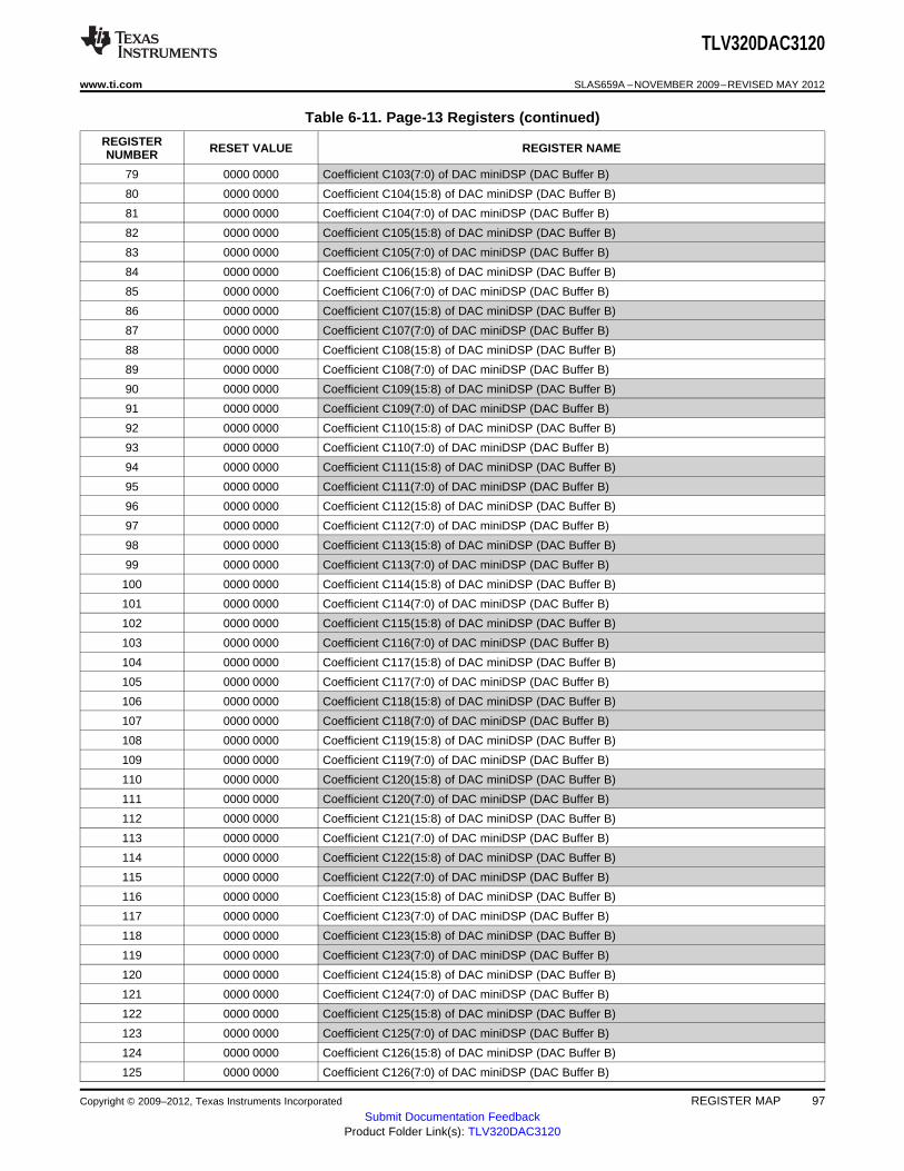
TLV320DAC3120
www.ti.com SLAS659A –NOVEMBER 2009–REVISED MAY 2012
Table 6-11. Page-13 Registers (continued)
REGISTER RESET VALUE REGISTER NAMENUMBER
79 0000 0000 Coefficient C103(7:0) of DAC miniDSP (DAC Buffer B)
80 0000 0000 Coefficient C104(15:8) of DAC miniDSP (DAC Buffer B)
81 0000 0000 Coefficient C104(7:0) of DAC miniDSP (DAC Buffer B)
82 0000 0000 Coefficient C105(15:8) of DAC miniDSP (DAC Buffer B)
83 0000 0000 Coefficient C105(7:0) of DAC miniDSP (DAC Buffer B)
84 0000 0000 Coefficient C106(15:8) of DAC miniDSP (DAC Buffer B)
85 0000 0000 Coefficient C106(7:0) of DAC miniDSP (DAC Buffer B)
86 0000 0000 Coefficient C107(15:8) of DAC miniDSP (DAC Buffer B)
87 0000 0000 Coefficient C107(7:0) of DAC miniDSP (DAC Buffer B)
88 0000 0000 Coefficient C108(15:8) of DAC miniDSP (DAC Buffer B)
89 0000 0000 Coefficient C108(7:0) of DAC miniDSP (DAC Buffer B)
90 0000 0000 Coefficient C109(15:8) of DAC miniDSP (DAC Buffer B)
91 0000 0000 Coefficient C109(7:0) of DAC miniDSP (DAC Buffer B)
92 0000 0000 Coefficient C110(15:8) of DAC miniDSP (DAC Buffer B)
93 0000 0000 Coefficient C110(7:0) of DAC miniDSP (DAC Buffer B)
94 0000 0000 Coefficient C111(15:8) of DAC miniDSP (DAC Buffer B)
95 0000 0000 Coefficient C111(7:0) of DAC miniDSP (DAC Buffer B)
96 0000 0000 Coefficient C112(15:8) of DAC miniDSP (DAC Buffer B)
97 0000 0000 Coefficient C112(7:0) of DAC miniDSP (DAC Buffer B)
98 0000 0000 Coefficient C113(15:8) of DAC miniDSP (DAC Buffer B)
99 0000 0000 Coefficient C113(7:0) of DAC miniDSP (DAC Buffer B)
100 0000 0000 Coefficient C114(15:8) of DAC miniDSP (DAC Buffer B)
101 0000 0000 Coefficient C114(7:0) of DAC miniDSP (DAC Buffer B)
102 0000 0000 Coefficient C115(15:8) of DAC miniDSP (DAC Buffer B)
103 0000 0000 Coefficient C116(7:0) of DAC miniDSP (DAC Buffer B)
104 0000 0000 Coefficient C117(15:8) of DAC miniDSP (DAC Buffer B)
105 0000 0000 Coefficient C117(7:0) of DAC miniDSP (DAC Buffer B)
106 0000 0000 Coefficient C118(15:8) of DAC miniDSP (DAC Buffer B)
107 0000 0000 Coefficient C118(7:0) of DAC miniDSP (DAC Buffer B)
108 0000 0000 Coefficient C119(15:8) of DAC miniDSP (DAC Buffer B)
109 0000 0000 Coefficient C119(7:0) of DAC miniDSP (DAC Buffer B)
110 0000 0000 Coefficient C120(15:8) of DAC miniDSP (DAC Buffer B)
111 0000 0000 Coefficient C120(7:0) of DAC miniDSP (DAC Buffer B)
112 0000 0000 Coefficient C121(15:8) of DAC miniDSP (DAC Buffer B)
113 0000 0000 Coefficient C121(7:0) of DAC miniDSP (DAC Buffer B)
114 0000 0000 Coefficient C122(15:8) of DAC miniDSP (DAC Buffer B)
115 0000 0000 Coefficient C122(7:0) of DAC miniDSP (DAC Buffer B)
116 0000 0000 Coefficient C123(15:8) of DAC miniDSP (DAC Buffer B)
117 0000 0000 Coefficient C123(7:0) of DAC miniDSP (DAC Buffer B)
118 0000 0000 Coefficient C123(15:8) of DAC miniDSP (DAC Buffer B)
119 0000 0000 Coefficient C123(7:0) of DAC miniDSP (DAC Buffer B)
120 0000 0000 Coefficient C124(15:8) of DAC miniDSP (DAC Buffer B)
121 0000 0000 Coefficient C124(7:0) of DAC miniDSP (DAC Buffer B)
122 0000 0000 Coefficient C125(15:8) of DAC miniDSP (DAC Buffer B)
123 0000 0000 Coefficient C125(7:0) of DAC miniDSP (DAC Buffer B)
124 0000 0000 Coefficient C126(15:8) of DAC miniDSP (DAC Buffer B)
125 0000 0000 Coefficient C126(7:0) of DAC miniDSP (DAC Buffer B)
Copyright © 2009–2012, Texas Instruments Incorporated REGISTER MAP 97Submit Documentation Feedback
Product Folder Link(s): TLV320DAC3120
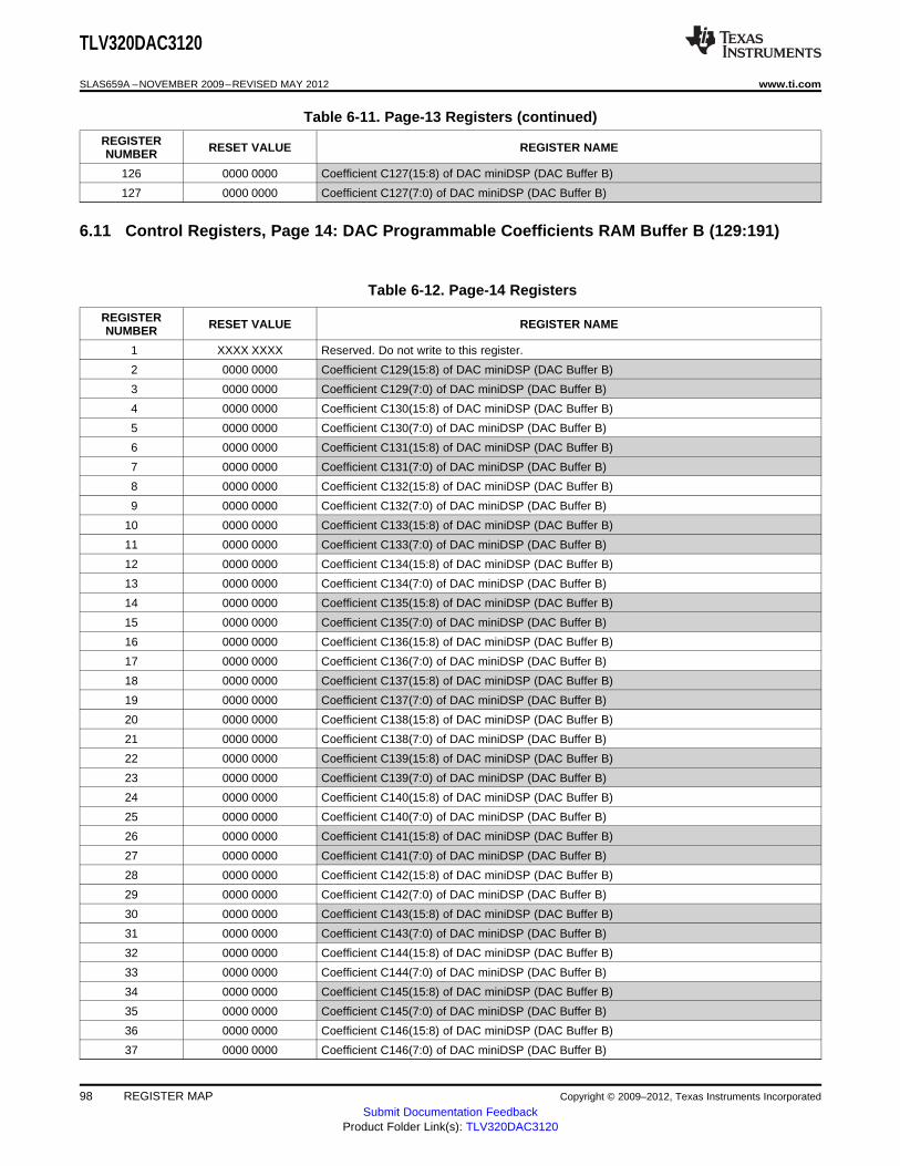
TLV320DAC3120
SLAS659A –NOVEMBER 2009–REVISED MAY 2012 www.ti.com
Table 6-11. Page-13 Registers (continued)
REGISTER RESET VALUE REGISTER NAMENUMBER
126 0000 0000 Coefficient C127(15:8) of DAC miniDSP (DAC Buffer B)
127 0000 0000 Coefficient C127(7:0) of DAC miniDSP (DAC Buffer B)
6.11 Control Registers, Page 14: DAC Programmable Coefficients RAM Buffer B (129:191)
Table 6-12. Page-14 Registers
REGISTER RESET VALUE REGISTER NAMENUMBER
1 XXXX XXXX Reserved. Do not write to this register.
2 0000 0000 Coefficient C129(15:8) of DAC miniDSP (DAC Buffer B)
3 0000 0000 Coefficient C129(7:0) of DAC miniDSP (DAC Buffer B)
4 0000 0000 Coefficient C130(15:8) of DAC miniDSP (DAC Buffer B)
5 0000 0000 Coefficient C130(7:0) of DAC miniDSP (DAC Buffer B)
6 0000 0000 Coefficient C131(15:8) of DAC miniDSP (DAC Buffer B)
7 0000 0000 Coefficient C131(7:0) of DAC miniDSP (DAC Buffer B)
8 0000 0000 Coefficient C132(15:8) of DAC miniDSP (DAC Buffer B)
9 0000 0000 Coefficient C132(7:0) of DAC miniDSP (DAC Buffer B)
10 0000 0000 Coefficient C133(15:8) of DAC miniDSP (DAC Buffer B)
11 0000 0000 Coefficient C133(7:0) of DAC miniDSP (DAC Buffer B)
12 0000 0000 Coefficient C134(15:8) of DAC miniDSP (DAC Buffer B)
13 0000 0000 Coefficient C134(7:0) of DAC miniDSP (DAC Buffer B)
14 0000 0000 Coefficient C135(15:8) of DAC miniDSP (DAC Buffer B)
15 0000 0000 Coefficient C135(7:0) of DAC miniDSP (DAC Buffer B)
16 0000 0000 Coefficient C136(15:8) of DAC miniDSP (DAC Buffer B)
17 0000 0000 Coefficient C136(7:0) of DAC miniDSP (DAC Buffer B)
18 0000 0000 Coefficient C137(15:8) of DAC miniDSP (DAC Buffer B)
19 0000 0000 Coefficient C137(7:0) of DAC miniDSP (DAC Buffer B)
20 0000 0000 Coefficient C138(15:8) of DAC miniDSP (DAC Buffer B)
21 0000 0000 Coefficient C138(7:0) of DAC miniDSP (DAC Buffer B)
22 0000 0000 Coefficient C139(15:8) of DAC miniDSP (DAC Buffer B)
23 0000 0000 Coefficient C139(7:0) of DAC miniDSP (DAC Buffer B)
24 0000 0000 Coefficient C140(15:8) of DAC miniDSP (DAC Buffer B)
25 0000 0000 Coefficient C140(7:0) of DAC miniDSP (DAC Buffer B)
26 0000 0000 Coefficient C141(15:8) of DAC miniDSP (DAC Buffer B)
27 0000 0000 Coefficient C141(7:0) of DAC miniDSP (DAC Buffer B)
28 0000 0000 Coefficient C142(15:8) of DAC miniDSP (DAC Buffer B)
29 0000 0000 Coefficient C142(7:0) of DAC miniDSP (DAC Buffer B)
30 0000 0000 Coefficient C143(15:8) of DAC miniDSP (DAC Buffer B)
31 0000 0000 Coefficient C143(7:0) of DAC miniDSP (DAC Buffer B)
32 0000 0000 Coefficient C144(15:8) of DAC miniDSP (DAC Buffer B)
33 0000 0000 Coefficient C144(7:0) of DAC miniDSP (DAC Buffer B)
34 0000 0000 Coefficient C145(15:8) of DAC miniDSP (DAC Buffer B)
35 0000 0000 Coefficient C145(7:0) of DAC miniDSP (DAC Buffer B)
36 0000 0000 Coefficient C146(15:8) of DAC miniDSP (DAC Buffer B)
37 0000 0000 Coefficient C146(7:0) of DAC miniDSP (DAC Buffer B)
98 REGISTER MAP Copyright © 2009–2012, Texas Instruments Incorporated
Submit Documentation FeedbackProduct Folder Link(s): TLV320DAC3120

TLV320DAC3120
www.ti.com SLAS659A –NOVEMBER 2009–REVISED MAY 2012
Table 6-12. Page-14 Registers (continued)
REGISTER RESET VALUE REGISTER NAMENUMBER
38 0000 0000 Coefficient C147(15:8) of DAC miniDSP (DAC Buffer B)
39 0000 0000 Coefficient C147(7:0) of DAC miniDSP (DAC Buffer B)
40 0000 0000 Coefficient C148(15:8) of DAC miniDSP (DAC Buffer B)
41 0000 0000 Coefficient C148(7:0) of DAC miniDSP (DAC Buffer B)
42 0000 0000 Coefficient C149(15:8) of DAC miniDSP (DAC Buffer B)
43 0000 0000 Coefficient C149(7:0) of DAC miniDSP (DAC Buffer B)
44 0000 0000 Coefficient C150(15:8) of DAC miniDSP (DAC Buffer B)
45 0000 0000 Coefficient C150(7:0) of DAC miniDSP (DAC Buffer B)
46 0000 0000 Coefficient C151(15:8) of DAC miniDSP (DAC Buffer B)
47 0000 0000 Coefficient C151(7:0) of DAC miniDSP (DAC Buffer B)
48 0000 0000 Coefficient C152(15:8) of DAC miniDSP (DAC Buffer B)
49 0000 0000 Coefficient C152(7:0) of DAC miniDSP (DAC Buffer B)
50 0000 0000 Coefficient C153(15:8) of DAC miniDSP (DAC Buffer B)
51 0000 0000 Coefficient C153(7:0) of DAC miniDSP (DAC Buffer B)
52 0000 0000 Coefficient C154(15:8) of DAC miniDSP (DAC Buffer B)
53 0000 0000 Coefficient C154(7:0) of DAC miniDSP (DAC Buffer B)
54 0000 0000 Coefficient C155(15:8) of DAC miniDSP (DAC Buffer B)
55 0000 0000 Coefficient C155(7:0) of DAC miniDSP (DAC Buffer B)
56 0000 0000 Coefficient C156(15:8) of DAC miniDSP (DAC Buffer B)
57 0000 0000 Coefficient C156(7:0) of DAC miniDSP (DAC Buffer B)
58 0000 0000 Coefficient C157(15:8) of DAC miniDSP (DAC Buffer B)
59 0000 0000 Coefficient C157(7:0) of DAC miniDSP (DAC Buffer B)
60 0000 0000 Coefficient C158(15:8) of DAC miniDSP (DAC Buffer B)
61 0000 0000 Coefficient C158(7:0) of DAC miniDSP (DAC Buffer B)
62 0000 0000 Coefficient C159(15:8) of DAC miniDSP (DAC Buffer B)
63 0000 0000 Coefficient C159(7:0) of DAC miniDSP (DAC Buffer B)
64 0000 0000 Coefficient C160(15:8) of DAC miniDSP (DAC Buffer B)
65 0000 0000 Coefficient C160(7:0) of DAC miniDSP (DAC Buffer B)
66 0000 0000 Coefficient C161(15:8) of DAC miniDSP (DAC Buffer B)
67 0000 0000 Coefficient C161(7:0) of DAC miniDSP (DAC Buffer B)
68 0000 0000 Coefficient C162(15:8) of DAC miniDSP (DAC Buffer B)
69 0000 0000 Coefficient C162(7:0) of DAC miniDSP (DAC Buffer B)
70 0000 0000 Coefficient C163(15:8) of DAC miniDSP (DAC Buffer B)
71 0000 0000 Coefficient C163(7:0) of DAC miniDSP (DAC Buffer B)
72 0000 0000 Coefficient C164(15:8) of DAC miniDSP (DAC Buffer B)
73 0000 0000 Coefficient C164(7:0) of DAC miniDSP (DAC Buffer B)
74 0000 0000 Coefficient C165(15:8) of DAC miniDSP (DAC Buffer B)
75 0000 0000 Coefficient C165(7:0) of DAC miniDSP (DAC Buffer B)
76 0000 0000 Coefficient C166(15:8) of DAC miniDSP (DAC Buffer B)
77 0000 0000 Coefficient C166(7:0) of DAC miniDSP (DAC Buffer B)
78 0000 0000 Coefficient C167(15:8) of DAC miniDSP (DAC Buffer B)
79 0000 0000 Coefficient C167(7:0) of DAC miniDSP (DAC Buffer B)
80 0000 0000 Coefficient C168(15:8) of DAC miniDSP (DAC Buffer B)
81 0000 0000 Coefficient C168(7:0) of DAC miniDSP (DAC Buffer B)
82 0000 0000 Coefficient C169(15:8) of DAC miniDSP (DAC Buffer B)
83 0000 0000 Coefficient C169(7:0) of DAC miniDSP (DAC Buffer B)
84 0000 0000 Coefficient C170(15:8) of DAC miniDSP (DAC Buffer B)
Copyright © 2009–2012, Texas Instruments Incorporated REGISTER MAP 99Submit Documentation Feedback
Product Folder Link(s): TLV320DAC3120
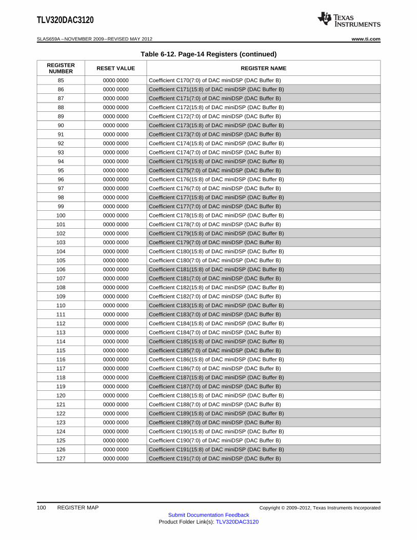
TLV320DAC3120
SLAS659A –NOVEMBER 2009–REVISED MAY 2012 www.ti.com
Table 6-12. Page-14 Registers (continued)
REGISTER RESET VALUE REGISTER NAMENUMBER
85 0000 0000 Coefficient C170(7:0) of DAC miniDSP (DAC Buffer B)
86 0000 0000 Coefficient C171(15:8) of DAC miniDSP (DAC Buffer B)
87 0000 0000 Coefficient C171(7:0) of DAC miniDSP (DAC Buffer B)
88 0000 0000 Coefficient C172(15:8) of DAC miniDSP (DAC Buffer B)
89 0000 0000 Coefficient C172(7:0) of DAC miniDSP (DAC Buffer B)
90 0000 0000 Coefficient C173(15:8) of DAC miniDSP (DAC Buffer B)
91 0000 0000 Coefficient C173(7:0) of DAC miniDSP (DAC Buffer B)
92 0000 0000 Coefficient C174(15:8) of DAC miniDSP (DAC Buffer B)
93 0000 0000 Coefficient C174(7:0) of DAC miniDSP (DAC Buffer B)
94 0000 0000 Coefficient C175(15:8) of DAC miniDSP (DAC Buffer B)
95 0000 0000 Coefficient C175(7:0) of DAC miniDSP (DAC Buffer B)
96 0000 0000 Coefficient C176(15:8) of DAC miniDSP (DAC Buffer B)
97 0000 0000 Coefficient C176(7:0) of DAC miniDSP (DAC Buffer B)
98 0000 0000 Coefficient C177(15:8) of DAC miniDSP (DAC Buffer B)
99 0000 0000 Coefficient C177(7:0) of DAC miniDSP (DAC Buffer B)
100 0000 0000 Coefficient C178(15:8) of DAC miniDSP (DAC Buffer B)
101 0000 0000 Coefficient C178(7:0) of DAC miniDSP (DAC Buffer B)
102 0000 0000 Coefficient C179(15:8) of DAC miniDSP (DAC Buffer B)
103 0000 0000 Coefficient C179(7:0) of DAC miniDSP (DAC Buffer B)
104 0000 0000 Coefficient C180(15:8) of DAC miniDSP (DAC Buffer B)
105 0000 0000 Coefficient C180(7:0) of DAC miniDSP (DAC Buffer B)
106 0000 0000 Coefficient C181(15:8) of DAC miniDSP (DAC Buffer B)
107 0000 0000 Coefficient C181(7:0) of DAC miniDSP (DAC Buffer B)
108 0000 0000 Coefficient C182(15:8) of DAC miniDSP (DAC Buffer B)
109 0000 0000 Coefficient C182(7:0) of DAC miniDSP (DAC Buffer B)
110 0000 0000 Coefficient C183(15:8) of DAC miniDSP (DAC Buffer B)
111 0000 0000 Coefficient C183(7:0) of DAC miniDSP (DAC Buffer B)
112 0000 0000 Coefficient C184(15:8) of DAC miniDSP (DAC Buffer B)
113 0000 0000 Coefficient C184(7:0) of DAC miniDSP (DAC Buffer B)
114 0000 0000 Coefficient C185(15:8) of DAC miniDSP (DAC Buffer B)
115 0000 0000 Coefficient C185(7:0) of DAC miniDSP (DAC Buffer B)
116 0000 0000 Coefficient C186(15:8) of DAC miniDSP (DAC Buffer B)
117 0000 0000 Coefficient C186(7:0) of DAC miniDSP (DAC Buffer B)
118 0000 0000 Coefficient C187(15:8) of DAC miniDSP (DAC Buffer B)
119 0000 0000 Coefficient C187(7:0) of DAC miniDSP (DAC Buffer B)
120 0000 0000 Coefficient C188(15:8) of DAC miniDSP (DAC Buffer B)
121 0000 0000 Coefficient C188(7:0) of DAC miniDSP (DAC Buffer B)
122 0000 0000 Coefficient C189(15:8) of DAC miniDSP (DAC Buffer B)
123 0000 0000 Coefficient C189(7:0) of DAC miniDSP (DAC Buffer B)
124 0000 0000 Coefficient C190(15:8) of DAC miniDSP (DAC Buffer B)
125 0000 0000 Coefficient C190(7:0) of DAC miniDSP (DAC Buffer B)
126 0000 0000 Coefficient C191(15:8) of DAC miniDSP (DAC Buffer B)
127 0000 0000 Coefficient C191(7:0) of DAC miniDSP (DAC Buffer B)
100 REGISTER MAP Copyright © 2009–2012, Texas Instruments Incorporated
Submit Documentation FeedbackProduct Folder Link(s): TLV320DAC3120
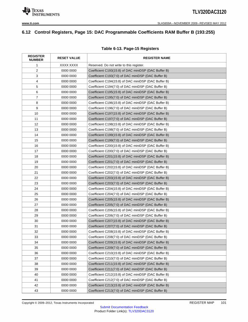
TLV320DAC3120
www.ti.com SLAS659A –NOVEMBER 2009–REVISED MAY 2012
6.12 Control Registers, Page 15: DAC Programmable Coefficients RAM Buffer B (193:255)
Table 6-13. Page-15 Registers
REGISTER RESET VALUE REGISTER NAMENUMBER
1 XXXX XXXX Reserved. Do not write to this register.
2 0000 0000 Coefficient C193(15:8) of DAC miniDSP (DAC Buffer B)
3 0000 0000 Coefficient C193(7:0) of DAC miniDSP (DAC Buffer B)
4 0000 0000 Coefficient C194(15:8) of DAC miniDSP (DAC Buffer B)
5 0000 0000 Coefficient C194(7:0) of DAC miniDSP (DAC Buffer B)
6 0000 0000 Coefficient C195(15:8) of DAC miniDSP (DAC Buffer B)
7 0000 0000 Coefficient C195(7:0) of DAC miniDSP (DAC Buffer B)
8 0000 0000 Coefficient C196(15:8) of DAC miniDSP (DAC Buffer B)
9 0000 0000 Coefficient C196(7:0) of DAC miniDSP (DAC Buffer B)
10 0000 0000 Coefficient C197(15:8) of DAC miniDSP (DAC Buffer B)
11 0000 0000 Coefficient C197(7:0) of DAC miniDSP (DAC Buffer B)
12 0000 0000 Coefficient C198(15:8) of DAC miniDSP (DAC Buffer B)
13 0000 0000 Coefficient C198(7:0) of DAC miniDSP (DAC Buffer B)
14 0000 0000 Coefficient C199(15:8) of DAC miniDSP (DAC Buffer B)
15 0000 0000 Coefficient C199(7:0) of DAC miniDSP (DAC Buffer B)
16 0000 0000 Coefficient C200(15:8) of DAC miniDSP (DAC Buffer B)
17 0000 0000 Coefficient C200(7:0) of DAC miniDSP (DAC Buffer B)
18 0000 0000 Coefficient C201(15:8) of DAC miniDSP (DAC Buffer B)
19 0000 0000 Coefficient C201(7:0) of DAC miniDSP (DAC Buffer B)
20 0000 0000 Coefficient C202(15:8) of DAC miniDSP (DAC Buffer B)
21 0000 0000 Coefficient C202(7:0) of DAC miniDSP (DAC Buffer B)
22 0000 0000 Coefficient C203(15:8) of DAC miniDSP (DAC Buffer B)
23 0000 0000 Coefficient C203(7:0) of DAC miniDSP (DAC Buffer B)
24 0000 0000 Coefficient C204(15:8) of DAC miniDSP (DAC Buffer B)
25 0000 0000 Coefficient C204(7:0) of DAC miniDSP (DAC Buffer B)
26 0000 0000 Coefficient C205(15:8) of DAC miniDSP (DAC Buffer B)
27 0000 0000 Coefficient C205(7:0) of DAC miniDSP (DAC Buffer B)
28 0000 0000 Coefficient C206(15:8) of DAC miniDSP (DAC Buffer B)
29 0000 0000 Coefficient C206(7:0) of DAC miniDSP (DAC Buffer B)
30 0000 0000 Coefficient C207(15:8) of DAC miniDSP (DAC Buffer B)
31 0000 0000 Coefficient C207(7:0) of DAC miniDSP (DAC Buffer B)
32 0000 0000 Coefficient C208(15:8) of DAC miniDSP (DAC Buffer B)
33 0000 0000 Coefficient C208(7:0) of DAC miniDSP (DAC Buffer B)
34 0000 0000 Coefficient C209(15:8) of DAC miniDSP (DAC Buffer B)
35 0000 0000 Coefficient C209(7:0) of DAC miniDSP (DAC Buffer B)
36 0000 0000 Coefficient C210(15:8) of DAC miniDSP (DAC Buffer B)
37 0000 0000 Coefficient C210(7:0) of DAC miniDSP (DAC Buffer B)
38 0000 0000 Coefficient C211(15:8) of DAC miniDSP (DAC Buffer B)
39 0000 0000 Coefficient C211(7:0) of DAC miniDSP (DAC Buffer B)
40 0000 0000 Coefficient C212(15:8) of DAC miniDSP (DAC Buffer B)
41 0000 0000 Coefficient C212(7:0) of DAC miniDSP (DAC Buffer B)
42 0000 0000 Coefficient C213(15:8) of DAC miniDSP (DAC Buffer B)
43 0000 0000 Coefficient C213(7:0) of DAC miniDSP (DAC Buffer B)
Copyright © 2009–2012, Texas Instruments Incorporated REGISTER MAP 101Submit Documentation Feedback
Product Folder Link(s): TLV320DAC3120
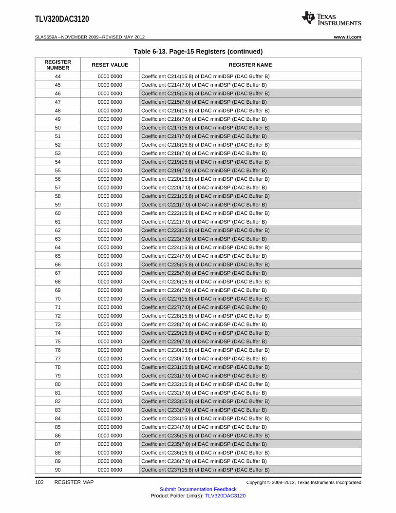
TLV320DAC3120
SLAS659A –NOVEMBER 2009–REVISED MAY 2012 www.ti.com
Table 6-13. Page-15 Registers (continued)
REGISTER RESET VALUE REGISTER NAMENUMBER
44 0000 0000 Coefficient C214(15:8) of DAC miniDSP (DAC Buffer B)
45 0000 0000 Coefficient C214(7:0) of DAC miniDSP (DAC Buffer B)
46 0000 0000 Coefficient C215(15:8) of DAC miniDSP (DAC Buffer B)
47 0000 0000 Coefficient C215(7:0) of DAC miniDSP (DAC Buffer B)
48 0000 0000 Coefficient C216(15:8) of DAC miniDSP (DAC Buffer B)
49 0000 0000 Coefficient C216(7:0) of DAC miniDSP (DAC Buffer B)
50 0000 0000 Coefficient C217(15:8) of DAC miniDSP (DAC Buffer B)
51 0000 0000 Coefficient C217(7:0) of DAC miniDSP (DAC Buffer B)
52 0000 0000 Coefficient C218(15:8) of DAC miniDSP (DAC Buffer B)
53 0000 0000 Coefficient C218(7:0) of DAC miniDSP (DAC Buffer B)
54 0000 0000 Coefficient C219(15:8) of DAC miniDSP (DAC Buffer B)
55 0000 0000 Coefficient C219(7:0) of DAC miniDSP (DAC Buffer B)
56 0000 0000 Coefficient C220(15:8) of DAC miniDSP (DAC Buffer B)
57 0000 0000 Coefficient C220(7:0) of DAC miniDSP (DAC Buffer B)
58 0000 0000 Coefficient C221(15:8) of DAC miniDSP (DAC Buffer B)
59 0000 0000 Coefficient C221(7:0) of DAC miniDSP (DAC Buffer B)
60 0000 0000 Coefficient C222(15:8) of DAC miniDSP (DAC Buffer B)
61 0000 0000 Coefficient C222(7:0) of DAC miniDSP (DAC Buffer B)
62 0000 0000 Coefficient C223(15:8) of DAC miniDSP (DAC Buffer B)
63 0000 0000 Coefficient C223(7:0) of DAC miniDSP (DAC Buffer B)
64 0000 0000 Coefficient C224(15:8) of DAC miniDSP (DAC Buffer B)
65 0000 0000 Coefficient C224(7:0) of DAC miniDSP (DAC Buffer B)
66 0000 0000 Coefficient C225(15:8) of DAC miniDSP (DAC Buffer B)
67 0000 0000 Coefficient C225(7:0) of DAC miniDSP (DAC Buffer B)
68 0000 0000 Coefficient C226(15:8) of DAC miniDSP (DAC Buffer B)
69 0000 0000 Coefficient C226(7:0) of DAC miniDSP (DAC Buffer B)
70 0000 0000 Coefficient C227(15:8) of DAC miniDSP (DAC Buffer B)
71 0000 0000 Coefficient C227(7:0) of DAC miniDSP (DAC Buffer B)
72 0000 0000 Coefficient C228(15:8) of DAC miniDSP (DAC Buffer B)
73 0000 0000 Coefficient C228(7:0) of DAC miniDSP (DAC Buffer B)
74 0000 0000 Coefficient C229(15:8) of DAC miniDSP (DAC Buffer B)
75 0000 0000 Coefficient C229(7:0) of DAC miniDSP (DAC Buffer B)
76 0000 0000 Coefficient C230(15:8) of DAC miniDSP (DAC Buffer B)
77 0000 0000 Coefficient C230(7:0) of DAC miniDSP (DAC Buffer B)
78 0000 0000 Coefficient C231(15:8) of DAC miniDSP (DAC Buffer B)
79 0000 0000 Coefficient C231(7:0) of DAC miniDSP (DAC Buffer B)
80 0000 0000 Coefficient C232(15:8) of DAC miniDSP (DAC Buffer B)
81 0000 0000 Coefficient C232(7:0) of DAC miniDSP (DAC Buffer B)
82 0000 0000 Coefficient C233(15:8) of DAC miniDSP (DAC Buffer B)
83 0000 0000 Coefficient C233(7:0) of DAC miniDSP (DAC Buffer B)
84 0000 0000 Coefficient C234(15:8) of DAC miniDSP (DAC Buffer B)
85 0000 0000 Coefficient C234(7:0) of DAC miniDSP (DAC Buffer B)
86 0000 0000 Coefficient C235(15:8) of DAC miniDSP (DAC Buffer B)
87 0000 0000 Coefficient C235(7:0) of DAC miniDSP (DAC Buffer B)
88 0000 0000 Coefficient C236(15:8) of DAC miniDSP (DAC Buffer B)
89 0000 0000 Coefficient C236(7:0) of DAC miniDSP (DAC Buffer B)
90 0000 0000 Coefficient C237(15:8) of DAC miniDSP (DAC Buffer B)
102 REGISTER MAP Copyright © 2009–2012, Texas Instruments Incorporated
Submit Documentation FeedbackProduct Folder Link(s): TLV320DAC3120
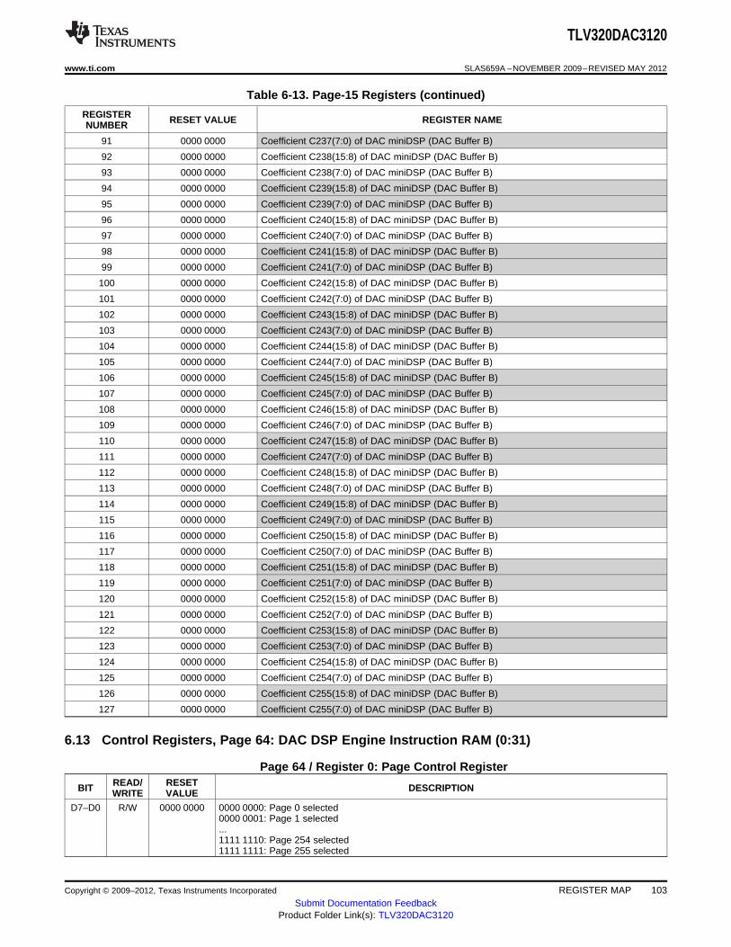
TLV320DAC3120
www.ti.com SLAS659A –NOVEMBER 2009–REVISED MAY 2012
Table 6-13. Page-15 Registers (continued)
REGISTER RESET VALUE REGISTER NAMENUMBER
91 0000 0000 Coefficient C237(7:0) of DAC miniDSP (DAC Buffer B)
92 0000 0000 Coefficient C238(15:8) of DAC miniDSP (DAC Buffer B)
93 0000 0000 Coefficient C238(7:0) of DAC miniDSP (DAC Buffer B)
94 0000 0000 Coefficient C239(15:8) of DAC miniDSP (DAC Buffer B)
95 0000 0000 Coefficient C239(7:0) of DAC miniDSP (DAC Buffer B)
96 0000 0000 Coefficient C240(15:8) of DAC miniDSP (DAC Buffer B)
97 0000 0000 Coefficient C240(7:0) of DAC miniDSP (DAC Buffer B)
98 0000 0000 Coefficient C241(15:8) of DAC miniDSP (DAC Buffer B)
99 0000 0000 Coefficient C241(7:0) of DAC miniDSP (DAC Buffer B)
100 0000 0000 Coefficient C242(15:8) of DAC miniDSP (DAC Buffer B)
101 0000 0000 Coefficient C242(7:0) of DAC miniDSP (DAC Buffer B)
102 0000 0000 Coefficient C243(15:8) of DAC miniDSP (DAC Buffer B)
103 0000 0000 Coefficient C243(7:0) of DAC miniDSP (DAC Buffer B)
104 0000 0000 Coefficient C244(15:8) of DAC miniDSP (DAC Buffer B)
105 0000 0000 Coefficient C244(7:0) of DAC miniDSP (DAC Buffer B)
106 0000 0000 Coefficient C245(15:8) of DAC miniDSP (DAC Buffer B)
107 0000 0000 Coefficient C245(7:0) of DAC miniDSP (DAC Buffer B)
108 0000 0000 Coefficient C246(15:8) of DAC miniDSP (DAC Buffer B)
109 0000 0000 Coefficient C246(7:0) of DAC miniDSP (DAC Buffer B)
110 0000 0000 Coefficient C247(15:8) of DAC miniDSP (DAC Buffer B)
111 0000 0000 Coefficient C247(7:0) of DAC miniDSP (DAC Buffer B)
112 0000 0000 Coefficient C248(15:8) of DAC miniDSP (DAC Buffer B)
113 0000 0000 Coefficient C248(7:0) of DAC miniDSP (DAC Buffer B)
114 0000 0000 Coefficient C249(15:8) of DAC miniDSP (DAC Buffer B)
115 0000 0000 Coefficient C249(7:0) of DAC miniDSP (DAC Buffer B)
116 0000 0000 Coefficient C250(15:8) of DAC miniDSP (DAC Buffer B)
117 0000 0000 Coefficient C250(7:0) of DAC miniDSP (DAC Buffer B)
118 0000 0000 Coefficient C251(15:8) of DAC miniDSP (DAC Buffer B)
119 0000 0000 Coefficient C251(7:0) of DAC miniDSP (DAC Buffer B)
120 0000 0000 Coefficient C252(15:8) of DAC miniDSP (DAC Buffer B)
121 0000 0000 Coefficient C252(7:0) of DAC miniDSP (DAC Buffer B)
122 0000 0000 Coefficient C253(15:8) of DAC miniDSP (DAC Buffer B)
123 0000 0000 Coefficient C253(7:0) of DAC miniDSP (DAC Buffer B)
124 0000 0000 Coefficient C254(15:8) of DAC miniDSP (DAC Buffer B)
125 0000 0000 Coefficient C254(7:0) of DAC miniDSP (DAC Buffer B)
126 0000 0000 Coefficient C255(15:8) of DAC miniDSP (DAC Buffer B)
127 0000 0000 Coefficient C255(7:0) of DAC miniDSP (DAC Buffer B)
6.13 Control Registers, Page 64: DAC DSP Engine Instruction RAM (0:31)
Page 64 / Register 0: Page Control RegisterREAD/ RESETBIT DESCRIPTIONWRITE VALUE
D7–D0 R/W 0000 0000 0000 0000: Page 0 selected0000 0001: Page 1 selected...1111 1110: Page 254 selected1111 1111: Page 255 selected
Copyright © 2009–2012, Texas Instruments Incorporated REGISTER MAP 103Submit Documentation Feedback
Product Folder Link(s): TLV320DAC3120
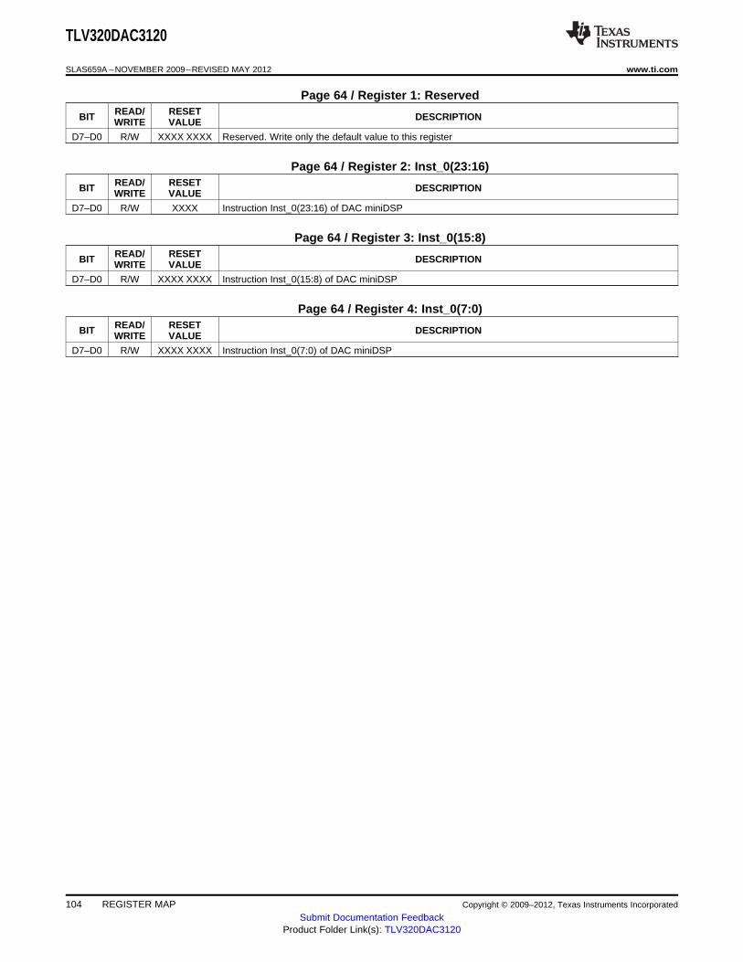
TLV320DAC3120
SLAS659A –NOVEMBER 2009–REVISED MAY 2012 www.ti.com
Page 64 / Register 1: ReservedREAD/ RESETBIT DESCRIPTIONWRITE VALUE
D7–D0 R/W XXXX XXXX Reserved. Write only the default value to this register
Page 64 / Register 2: Inst_0(23:16)READ/ RESETBIT DESCRIPTIONWRITE VALUE
D7–D0 R/W XXXX Instruction Inst_0(23:16) of DAC miniDSP
Page 64 / Register 3: Inst_0(15:8)READ/ RESETBIT DESCRIPTIONWRITE VALUE
D7–D0 R/W XXXX XXXX Instruction Inst_0(15:8) of DAC miniDSP
Page 64 / Register 4: Inst_0(7:0)READ/ RESETBIT DESCRIPTIONWRITE VALUE
D7–D0 R/W XXXX XXXX Instruction Inst_0(7:0) of DAC miniDSP
104 REGISTER MAP Copyright © 2009–2012, Texas Instruments Incorporated
Submit Documentation FeedbackProduct Folder Link(s): TLV320DAC3120
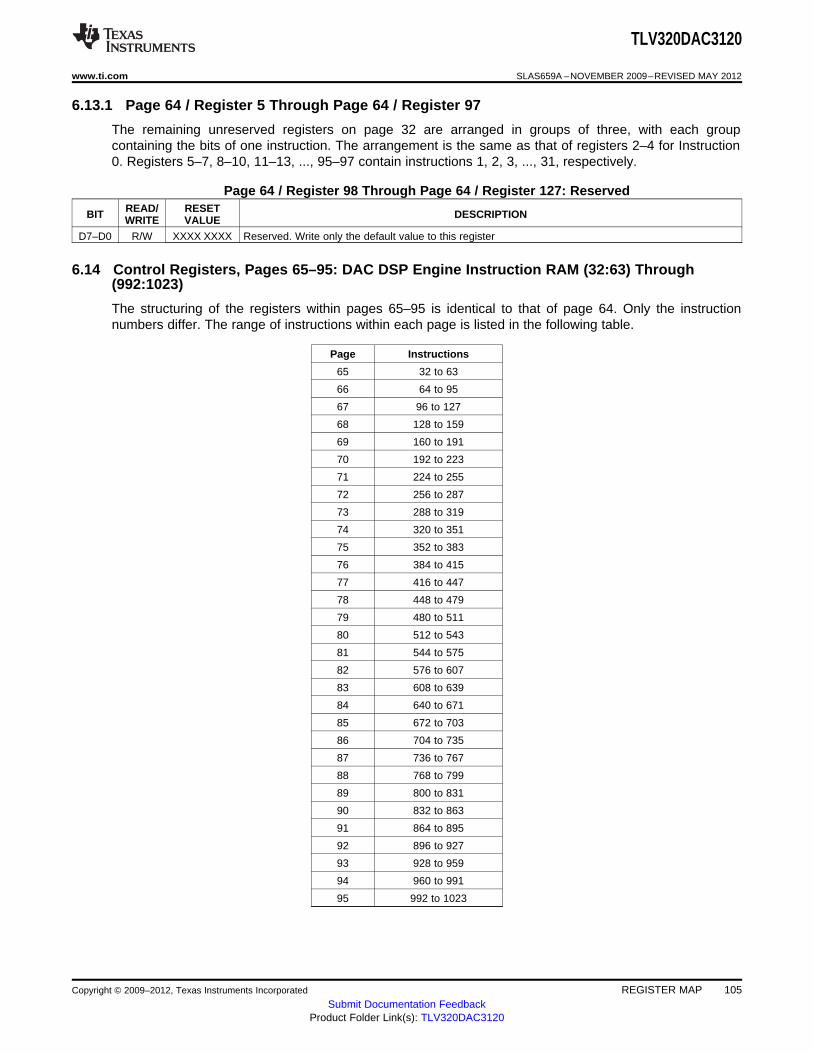
TLV320DAC3120
www.ti.com SLAS659A –NOVEMBER 2009–REVISED MAY 2012
6.13.1 Page 64 / Register 5 Through Page 64 / Register 97
The remaining unreserved registers on page 32 are arranged in groups of three, with each groupcontaining the bits of one instruction. The arrangement is the same as that of registers 2–4 for Instruction0. Registers 5–7, 8–10, 11–13, ..., 95–97 contain instructions 1, 2, 3, ..., 31, respectively.
Page 64 / Register 98 Through Page 64 / Register 127: ReservedREAD/ RESETBIT DESCRIPTIONWRITE VALUE
D7–D0 R/W XXXX XXXX Reserved. Write only the default value to this register
6.14 Control Registers, Pages 65–95: DAC DSP Engine Instruction RAM (32:63) Through(992:1023)
The structuring of the registers within pages 65–95 is identical to that of page 64. Only the instructionnumbers differ. The range of instructions within each page is listed in the following table.
Page Instructions
65 32 to 63
66 64 to 95
67 96 to 127
68 128 to 159
69 160 to 191
70 192 to 223
71 224 to 255
72 256 to 287
73 288 to 319
74 320 to 351
75 352 to 383
76 384 to 415
77 416 to 447
78 448 to 479
79 480 to 511
80 512 to 543
81 544 to 575
82 576 to 607
83 608 to 639
84 640 to 671
85 672 to 703
86 704 to 735
87 736 to 767
88 768 to 799
89 800 to 831
90 832 to 863
91 864 to 895
92 896 to 927
93 928 to 959
94 960 to 991
95 992 to 1023
Copyright © 2009–2012, Texas Instruments Incorporated REGISTER MAP 105Submit Documentation Feedback
Product Folder Link(s): TLV320DAC3120
TLV320DAC3120
SLAS659A –NOVEMBER 2009–REVISED MAY 2012 www.ti.com
Revision HistoryNOTE: Page numbers for previous revisions may differ from page numbers in the current version.
Changes from Original (November, 2009) to Revision A Page
• Added extra bullet point to Features. .......................................................................................... 1• Changed Register 36 to register 35 in section 5.5.2. ...................................................................... 21• Added extra row to the end of Table 5-6. .................................................................................... 23• Added subsection 5.6.1.2.9 and image. ...................................................................................... 25• Added section 5.6.7 from SLAS644C after Interrupts section. .......................................................... 36• Added D6–D0 to the Register Value column heading and changed Analog Attenuation to Analog Gain. ..... 40• Deleted Analog Volume Control for Headphone and Speaker Outputs (for D7=0) table and added table
note to D7 = 1 table. .............................................................................................................. 40• Changed page 0 to page 1 in section 5.6.9.1. ............................................................................... 41• Added Timer section and image after PLL section. ....................................................................... 47• Changed last line to "10111-11000: Reserved. Do not use." "11001: DAC Signal Processing Block
PRB_P25" "11010-11111: Reserved. Do not use." ......................................................................... 67• Added Beep Generator bit registers from DAC3100 (Page 0 / Register 71, and 73-79). ............................ 70• Added reserved tables. .......................................................................................................... 71• Changed D0=1 to Reserved in Page 1 / Register 33. ...................................................................... 73• Removed extraneous cross-references for deleted table. ................................................................ 74• Added footnote to Page 1 / Register 40: HPOUT Driver. .................................................................. 74• Changed registers 66-127 to Reserved in Table 6-6. ...................................................................... 81• Changed registers 8-13 to Reserved in Table 6-7. ......................................................................... 82• Changed registers 66-127 to Reserved in Table 6-10. ..................................................................... 94• Changed registers 8-13 to Reserved in Table 6-11. ........................................................................ 95
106 REGISTER MAP Copyright © 2009–2012, Texas Instruments Incorporated
Submit Documentation FeedbackProduct Folder Link(s): TLV320DAC3120
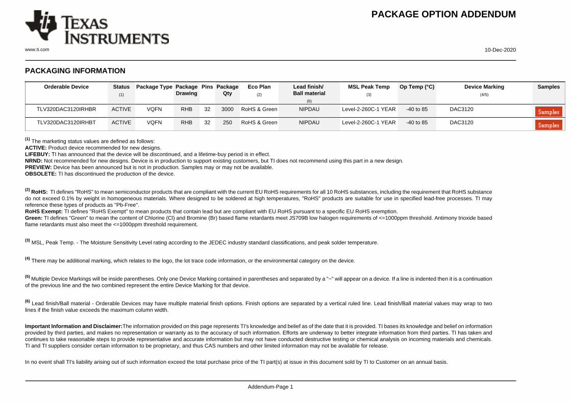
PACKAGE OPTION ADDENDUM
www.ti.com 10-Dec-2020
Addendum-Page 1
PACKAGING INFORMATION
Orderable Device Status(1)
Package Type PackageDrawing
Pins PackageQty
Eco Plan(2)
Lead finish/Ball material
(6)
MSL Peak Temp(3)
Op Temp (°C) Device Marking(4/5)
Samples
TLV320DAC3120IRHBR ACTIVE VQFN RHB 32 3000 RoHS & Green NIPDAU Level-2-260C-1 YEAR -40 to 85 DAC3120
TLV320DAC3120IRHBT ACTIVE VQFN RHB 32 250 RoHS & Green NIPDAU Level-2-260C-1 YEAR -40 to 85 DAC3120
(1) The marketing status values are defined as follows:ACTIVE: Product device recommended for new designs.LIFEBUY: TI has announced that the device will be discontinued, and a lifetime-buy period is in effect.NRND: Not recommended for new designs. Device is in production to support existing customers, but TI does not recommend using this part in a new design.PREVIEW: Device has been announced but is not in production. Samples may or may not be available.OBSOLETE: TI has discontinued the production of the device.
(2) RoHS: TI defines "RoHS" to mean semiconductor products that are compliant with the current EU RoHS requirements for all 10 RoHS substances, including the requirement that RoHS substancedo not exceed 0.1% by weight in homogeneous materials. Where designed to be soldered at high temperatures, "RoHS" products are suitable for use in specified lead-free processes. TI mayreference these types of products as "Pb-Free".RoHS Exempt: TI defines "RoHS Exempt" to mean products that contain lead but are compliant with EU RoHS pursuant to a specific EU RoHS exemption.Green: TI defines "Green" to mean the content of Chlorine (Cl) and Bromine (Br) based flame retardants meet JS709B low halogen requirements of <=1000ppm threshold. Antimony trioxide basedflame retardants must also meet the <=1000ppm threshold requirement.
(3) MSL, Peak Temp. - The Moisture Sensitivity Level rating according to the JEDEC industry standard classifications, and peak solder temperature.
(4) There may be additional marking, which relates to the logo, the lot trace code information, or the environmental category on the device.
(5) Multiple Device Markings will be inside parentheses. Only one Device Marking contained in parentheses and separated by a "~" will appear on a device. If a line is indented then it is a continuationof the previous line and the two combined represent the entire Device Marking for that device.
(6) Lead finish/Ball material - Orderable Devices may have multiple material finish options. Finish options are separated by a vertical ruled line. Lead finish/Ball material values may wrap to twolines if the finish value exceeds the maximum column width.
Important Information and Disclaimer:The information provided on this page represents TI's knowledge and belief as of the date that it is provided. TI bases its knowledge and belief on informationprovided by third parties, and makes no representation or warranty as to the accuracy of such information. Efforts are underway to better integrate information from third parties. TI has taken andcontinues to take reasonable steps to provide representative and accurate information but may not have conducted destructive testing or chemical analysis on incoming materials and chemicals.TI and TI suppliers consider certain information to be proprietary, and thus CAS numbers and other limited information may not be available for release.
In no event shall TI's liability arising out of such information exceed the total purchase price of the TI part(s) at issue in this document sold by TI to Customer on an annual basis.
PACKAGE OPTION ADDENDUM
www.ti.com 10-Dec-2020
Addendum-Page 2
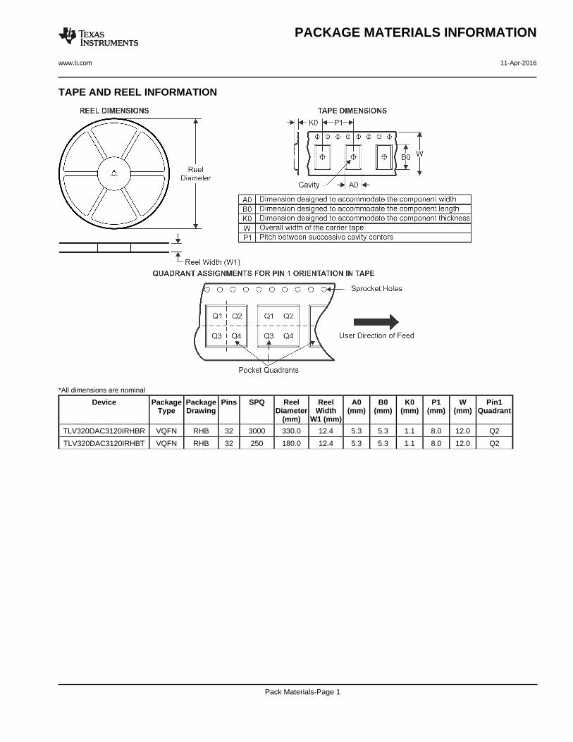
TAPE AND REEL INFORMATION
*All dimensions are nominal
Device PackageType
PackageDrawing
Pins SPQ ReelDiameter
(mm)
ReelWidth
W1 (mm)
A0(mm)
B0(mm)
K0(mm)
P1(mm)
W(mm)
Pin1Quadrant
TLV320DAC3120IRHBR VQFN RHB 32 3000 330.0 12.4 5.3 5.3 1.1 8.0 12.0 Q2
TLV320DAC3120IRHBT VQFN RHB 32 250 180.0 12.4 5.3 5.3 1.1 8.0 12.0 Q2
PACKAGE MATERIALS INFORMATION
www.ti.com 11-Apr-2016
Pack Materials-Page 1
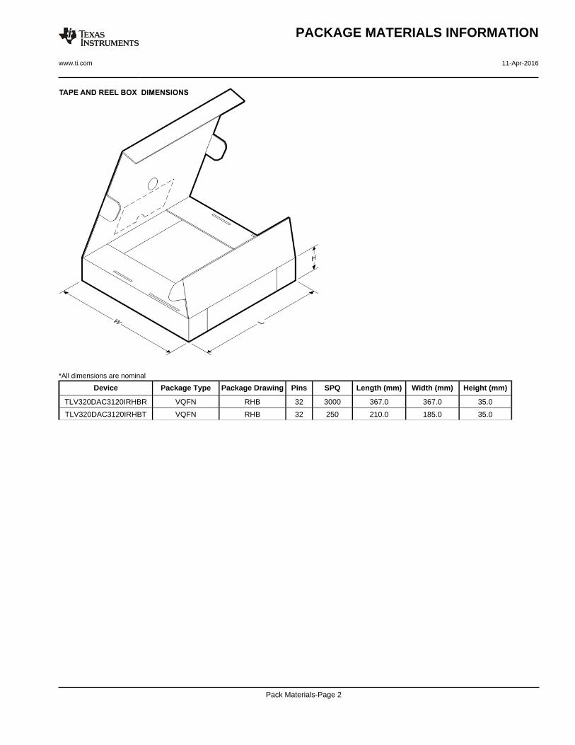
*All dimensions are nominal
Device Package Type Package Drawing Pins SPQ Length (mm) Width (mm) Height (mm)
TLV320DAC3120IRHBR VQFN RHB 32 3000 367.0 367.0 35.0
TLV320DAC3120IRHBT VQFN RHB 32 250 210.0 185.0 35.0
PACKAGE MATERIALS INFORMATION
www.ti.com 11-Apr-2016
Pack Materials-Page 2
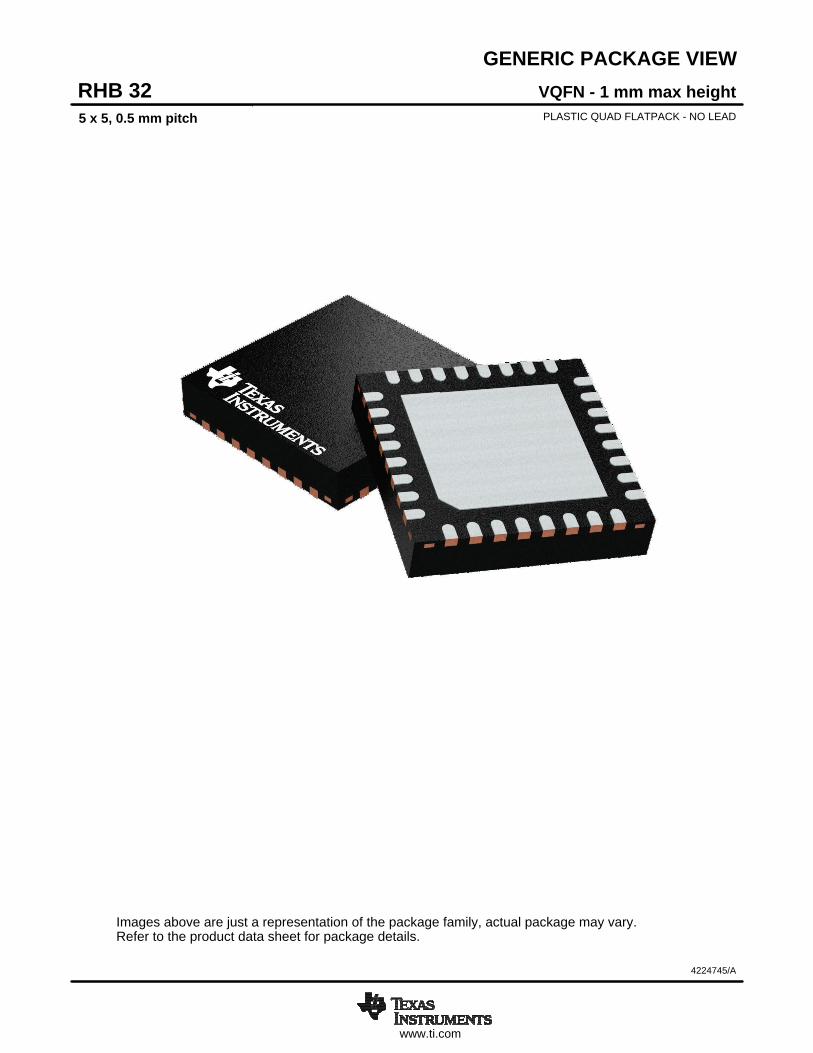
www.ti.com
GENERIC PACKAGE VIEW
Images above are just a representation of the package family, actual package may vary.Refer to the product data sheet for package details.
VQFN - 1 mm max heightRHB 32PLASTIC QUAD FLATPACK - NO LEAD5 x 5, 0.5 mm pitch
4224745/A
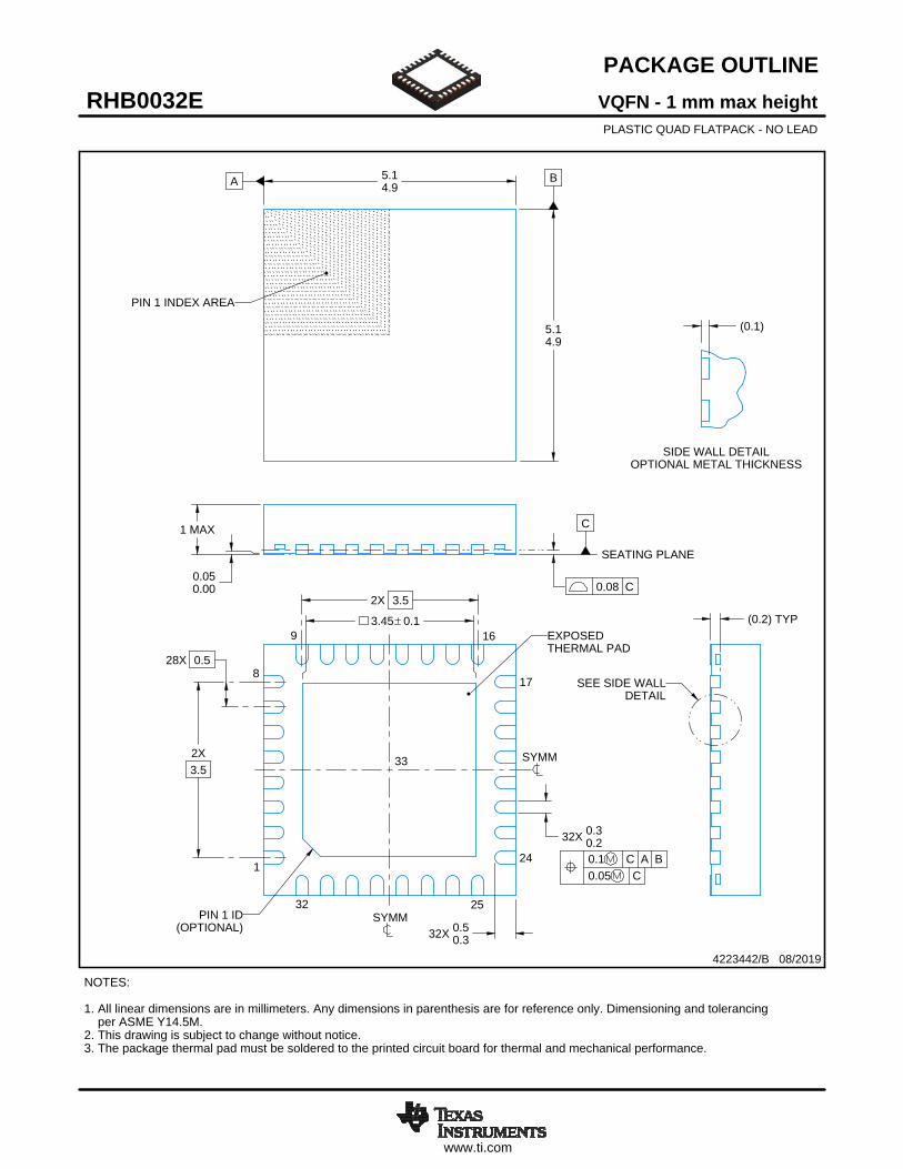
www.ti.com
PACKAGE OUTLINE
C
32X 0.30.2
3.45 0.1
32X 0.50.3
1 MAX
(0.2) TYP
0.050.00
28X 0.5
2X3.5
2X 3.5
A 5.14.9
B
5.14.9
(0.1)
VQFN - 1 mm max heightRHB0032EPLASTIC QUAD FLATPACK - NO LEAD
4223442/B 08/2019
PIN 1 INDEX AREA
0.08 C
SEATING PLANE
1
817
24
9 16
32 25
(OPTIONAL)PIN 1 ID
0.1 C A B0.05 C
EXPOSEDTHERMAL PAD
33 SYMM
SYMM
NOTES: 1. All linear dimensions are in millimeters. Any dimensions in parenthesis are for reference only. Dimensioning and tolerancing per ASME Y14.5M. 2. This drawing is subject to change without notice. 3. The package thermal pad must be soldered to the printed circuit board for thermal and mechanical performance.
SCALE 3.000
SEE SIDE WALLDETAIL
20.000
SIDE WALL DETAILOPTIONAL METAL THICKNESS
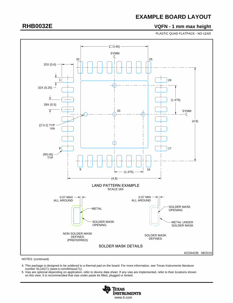
www.ti.com
EXAMPLE BOARD LAYOUT
(1.475)
0.07 MINALL AROUND
0.07 MAXALL AROUND
32X (0.25)
32X (0.6)
( 0.2) TYPVIA
28X (0.5)
(4.8)
(4.8)
(1.475)
( 3.45)
(R0.05)TYP
VQFN - 1 mm max heightRHB0032EPLASTIC QUAD FLATPACK - NO LEAD
4223442/B 08/2019
SYMM
1
8
9 16
17
24
2532
SYMM
LAND PATTERN EXAMPLESCALE:18X
NOTES: (continued) 4. This package is designed to be soldered to a thermal pad on the board. For more information, see Texas Instruments literature number SLUA271 (www.ti.com/lit/slua271).5. Vias are optional depending on application, refer to device data sheet. If any vias are implemented, refer to their locations shown on this view. It is recommended that vias under paste be filled, plugged or tented.
33
SOLDER MASKOPENING
METAL UNDERSOLDER MASK
SOLDER MASKDEFINED
METAL
SOLDER MASKOPENING
SOLDER MASK DETAILS
NON SOLDER MASKDEFINED
(PREFERRED)
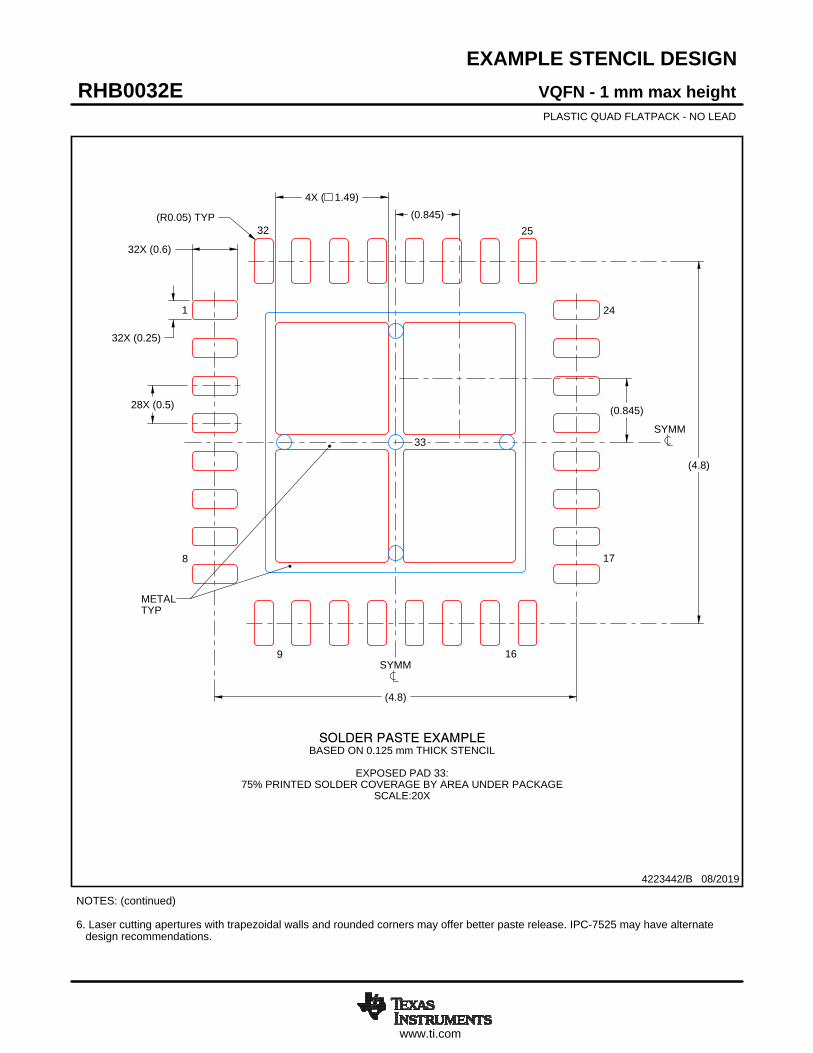
www.ti.com
EXAMPLE STENCIL DESIGN
32X (0.6)
32X (0.25)
28X (0.5)
(4.8)
(4.8)
4X ( 1.49)
(0.845)
(0.845)(R0.05) TYP
VQFN - 1 mm max heightRHB0032EPLASTIC QUAD FLATPACK - NO LEAD
4223442/B 08/2019
NOTES: (continued) 6. Laser cutting apertures with trapezoidal walls and rounded corners may offer better paste release. IPC-7525 may have alternate design recommendations.
33
SYMM
METALTYP
SOLDER PASTE EXAMPLEBASED ON 0.125 mm THICK STENCIL
EXPOSED PAD 33:
75% PRINTED SOLDER COVERAGE BY AREA UNDER PACKAGESCALE:20X
SYMM
1
8
9 16
17
24
2532
IMPORTANT NOTICE AND DISCLAIMER
TI PROVIDES TECHNICAL AND RELIABILITY DATA (INCLUDING DATASHEETS), DESIGN RESOURCES (INCLUDING REFERENCE DESIGNS), APPLICATION OR OTHER DESIGN ADVICE, WEB TOOLS, SAFETY INFORMATION, AND OTHER RESOURCES “AS IS” AND WITH ALL FAULTS, AND DISCLAIMS ALL WARRANTIES, EXPRESS AND IMPLIED, INCLUDING WITHOUT LIMITATION ANY IMPLIED WARRANTIES OF MERCHANTABILITY, FITNESS FOR A PARTICULAR PURPOSE OR NON-INFRINGEMENT OF THIRD PARTY INTELLECTUAL PROPERTY RIGHTS.These resources are intended for skilled developers designing with TI products. You are solely responsible for (1) selecting the appropriate TI products for your application, (2) designing, validating and testing your application, and (3) ensuring your application meets applicable standards, and any other safety, security, or other requirements. These resources are subject to change without notice. TI grants you permission to use these resources only for development of an application that uses the TI products described in the resource. Other reproduction and display of these resources is prohibited. No license is granted to any other TI intellectual property right or to any third party intellectual property right. TI disclaims responsibility for, and you will fully indemnify TI and its representatives against, any claims, damages, costs, losses, and liabilities arising out of your use of these resources.TI’s products are provided subject to TI’s Terms of Sale (www.ti.com/legal/termsofsale.html) or other applicable terms available either on ti.com or provided in conjunction with such TI products. TI’s provision of these resources does not expand or otherwise alter TI’s applicable warranties or warranty disclaimers for TI products.
Mailing Address: Texas Instruments, Post Office Box 655303, Dallas, Texas 75265Copyright © 2020, Texas Instruments Incorporated
Related Documents


