User's Guide SLAU564A – February 2014 – Revised February 2014 TLV320AIC3268EVM-U Evaluation Module This User’s Guide describes the operation, use, and features of the TLV320AIC3268EVM-U. For questions and support go to the E2E forums (e2e.ti.com). The main contents of this document are: • Hardware descriptions and implementation • Start up procedure using PurePath™ Console 2 (PPC2) software with the AIC3268 plug-in Table 1. Related Documents Document Title Literature Number TLV320AIC3268 Data Sheet SLAS953 PurePath Graphic Development Suite PurePath Console Contents 1 Features ...................................................................................................................... 2 2 Introduction .................................................................................................................. 2 2.1 Electrostatic Discharge Warning ................................................................................. 2 2.2 Unpacking the EVM ................................................................................................ 3 3 Getting Started .............................................................................................................. 4 4 PurePath Console 2 Software ............................................................................................. 4 4.1 Installation ........................................................................................................... 4 4.2 Graphical User Interface (GUI) ................................................................................... 5 5 TLV320AIC3268EVM-U Default Jumper Locations .................................................................... 7 6 TLV320AIC3268EVM-U EVM Schematics .............................................................................. 8 7 TLV320AIC3268EVM-U EVM Board Layout ........................................................................... 17 8 TLV320AIC3268EVM-U Bill of Materials ............................................................................... 19 9 Writing Scripts .............................................................................................................. 22 List of Figures 1 TLV320AIC3268EVM-U Top Board Photo .............................................................................. 3 2 TLV320AIC3268EVM-U Bottom Board Photo........................................................................... 3 3 Main Panel ................................................................................................................... 5 4 Register Inspector Window ................................................................................................ 6 5 TLV320AIC3268RGC Block Diagram .................................................................................... 8 6 TAS1020BPFB USB Controller ........................................................................................... 9 7 Sample Rate Converters for ASIs ....................................................................................... 10 8 GPIO and MCLK for AIC3268 ........................................................................................... 11 9 LDO Supplies and Analog Outputs ..................................................................................... 12 10 TLV320AIC3268 Schematic.............................................................................................. 13 11 Audio Connectors ......................................................................................................... 14 12 I 2 C Translation and Selection ............................................................................................ 15 13 Breakout Board Connections ............................................................................................ 16 14 Top Xray View ............................................................................................................. 17 PurePath is a trademark of Texas Instruments. Windows is a registered trademark of Microsoft Corporation. 1 SLAU564A – February 2014 – Revised February 2014 TLV320AIC3268EVM-U Evaluation Module Submit Documentation Feedback Copyright © 2014, Texas Instruments Incorporated

Welcome message from author
This document is posted to help you gain knowledge. Please leave a comment to let me know what you think about it! Share it to your friends and learn new things together.
Transcript
User's GuideSLAU564A–February 2014–Revised February 2014
TLV320AIC3268EVM-U Evaluation Module
This User’s Guide describes the operation, use, and features of the TLV320AIC3268EVM-U. Forquestions and support go to the E2E forums (e2e.ti.com).
The main contents of this document are:• Hardware descriptions and implementation• Start up procedure using PurePath™ Console 2 (PPC2) software with the AIC3268 plug-in
Table 1. Related DocumentsDocument Title Literature Number
TLV320AIC3268 Data Sheet SLAS953PurePath Graphic Development Suite PurePath Console
Contents1 Features ...................................................................................................................... 22 Introduction .................................................................................................................. 2
2.1 Electrostatic Discharge Warning ................................................................................. 22.2 Unpacking the EVM ................................................................................................ 3
3 Getting Started .............................................................................................................. 44 PurePath Console 2 Software ............................................................................................. 4
4.1 Installation ........................................................................................................... 44.2 Graphical User Interface (GUI) ................................................................................... 5
5 TLV320AIC3268EVM-U Default Jumper Locations .................................................................... 76 TLV320AIC3268EVM-U EVM Schematics .............................................................................. 87 TLV320AIC3268EVM-U EVM Board Layout ........................................................................... 178 TLV320AIC3268EVM-U Bill of Materials ............................................................................... 199 Writing Scripts .............................................................................................................. 22
List of Figures
1 TLV320AIC3268EVM-U Top Board Photo .............................................................................. 32 TLV320AIC3268EVM-U Bottom Board Photo........................................................................... 33 Main Panel ................................................................................................................... 54 Register Inspector Window ................................................................................................ 65 TLV320AIC3268RGC Block Diagram .................................................................................... 86 TAS1020BPFB USB Controller ........................................................................................... 97 Sample Rate Converters for ASIs ....................................................................................... 108 GPIO and MCLK for AIC3268 ........................................................................................... 119 LDO Supplies and Analog Outputs ..................................................................................... 1210 TLV320AIC3268 Schematic.............................................................................................. 1311 Audio Connectors ......................................................................................................... 1412 I2C Translation and Selection ............................................................................................ 1513 Breakout Board Connections ............................................................................................ 1614 Top Xray View ............................................................................................................. 17
PurePath is a trademark of Texas Instruments.Windows is a registered trademark of Microsoft Corporation.
1SLAU564A–February 2014–Revised February 2014 TLV320AIC3268EVM-U Evaluation ModuleSubmit Documentation Feedback
Copyright © 2014, Texas Instruments Incorporated
Features www.ti.com
15 Silkscreen Top ............................................................................................................. 1716 Silkscreen Bottom ......................................................................................................... 18
1 Features• Full featured EVM with the TLV320AIC3268 Audio Codec• USB connection to PC provides power, control and streaming audio for quick evaluation• Easy-to-use PurePath Console 2 software provides graphical user interface to configure and control
AIC3268
2 IntroductionThis specific evaluation module (EVM) is a programmable USB audio device that features theTLV320AIC3268 Audio Codec with miniDSP.
2.1 Electrostatic Discharge WarningMany of the components on the EVM are susceptible to damage by electrostatic discharge (ESD). Usersare advised to observe proper ESD handling precautions when unpacking and handling the EVM,including the use of a grounded wrist strap at an approved ESD workstation.
CAUTIONFailure to observe ESD handling procedures can result in damage to EVMcomponents.
2 TLV320AIC3268EVM-U Evaluation Module SLAU564A–February 2014–Revised February 2014Submit Documentation Feedback
Copyright © 2014, Texas Instruments Incorporated

www.ti.com Introduction
2.2 Unpacking the EVMOn opening the TLV320AIC3268EVM-U package, ensure that the following item is included:• One TLV320AIC3268EVM-U board using one TLV320AIC3268 (Figure 1 and Figure 2)
If either of the board or the TLV320AIC3268 device is missing, contact the Texas Instruments ProductInformation Center to inquire about a replacement.
Figure 1. TLV320AIC3268EVM-U Top Board Photo
Figure 2. TLV320AIC3268EVM-U Bottom Board Photo
3SLAU564A–February 2014–Revised February 2014 TLV320AIC3268EVM-U Evaluation ModuleSubmit Documentation Feedback
Copyright © 2014, Texas Instruments Incorporated

Getting Started www.ti.com
3 Getting Started
1. Request and download the PPC2 software located in the EVM product folder on the web.2. Connect the EVM to USB port, LED lights LED1 and LED2 should illuminate once the EVM is detected
by Windows® PC. Also, in the Windows Device Manager, the EVM should be recognized as a USBcomposite device, a USB audio device and an HID-compliant device.
3. Connect headphones to jack J7, labeled HP OUT.4. Open PPC2 and in the Command Buffer Interface select Open.5. Download the most up-to-date scripts from the product folder. Navigate to that folder and select script
1.1 and click Execute.6. Play audio through any media tool. Make sure that the playback (and recording) device is USB-
AudioEVM in the Windows control panel.• To adjust playback volume, open Sound in control panel, select the USB-AudioEVM device and
click Properties.• Similarly, the other example configurations can be tried and sound can be recorded using the
microphone available on the board.7. Install jumpers on the EVM as per the requirements to make the right signal connections.
4 PurePath Console 2 Software
4.1 Installation
1. Request and download the PPC2 software located in the TLV320AIC3268 product folder.2. Open the self-extracting installation file, and extract contents to a known folder.3. Install the software by double clicking the setup executable and follow the directions.4. Connect the EVM to a USB port using a micro-USB cable and open PurePath Console 2. If prompted,
select the appropriate EVM name.
4 TLV320AIC3268EVM-U Evaluation Module SLAU564A–February 2014–Revised February 2014Submit Documentation Feedback
Copyright © 2014, Texas Instruments Incorporated
www.ti.com PurePath Console 2 Software
4.2 Graphical User Interface (GUI)
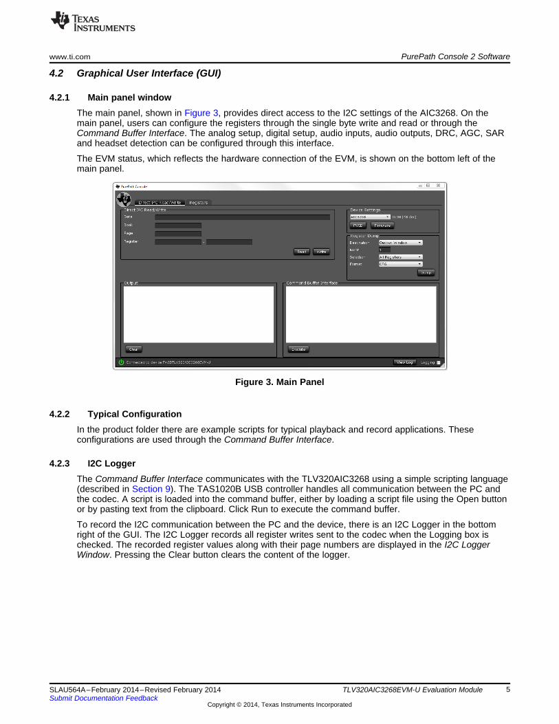
4.2.1 Main panel windowThe main panel, shown in Figure 3, provides direct access to the I2C settings of the AIC3268. On themain panel, users can configure the registers through the single byte write and read or through theCommand Buffer Interface. The analog setup, digital setup, audio inputs, audio outputs, DRC, AGC, SARand headset detection can be configured through this interface.
The EVM status, which reflects the hardware connection of the EVM, is shown on the bottom left of themain panel.
Figure 3. Main Panel
4.2.2 Typical ConfigurationIn the product folder there are example scripts for typical playback and record applications. Theseconfigurations are used through the Command Buffer Interface.
4.2.3 I2C LoggerThe Command Buffer Interface communicates with the TLV320AIC3268 using a simple scripting language(described in Section 9). The TAS1020B USB controller handles all communication between the PC andthe codec. A script is loaded into the command buffer, either by loading a script file using the Open buttonor by pasting text from the clipboard. Click Run to execute the command buffer.
To record the I2C communication between the PC and the device, there is an I2C Logger in the bottomright of the GUI. The I2C Logger records all register writes sent to the codec when the Logging box ischecked. The recorded register values along with their page numbers are displayed in the I2C LoggerWindow. Pressing the Clear button clears the content of the logger.
5SLAU564A–February 2014–Revised February 2014 TLV320AIC3268EVM-U Evaluation ModuleSubmit Documentation Feedback
Copyright © 2014, Texas Instruments Incorporated

PurePath Console 2 Software www.ti.com
4.2.4 Register Inspector
Figure 4. Register Inspector Window
The contents of the TLV320AIC3268 register map can be accessed through the Registers tab in PPC2.The Page number control selects the page to be displayed in the register table. The register table containsinformation such as register name, current register value and the bit field of the current register value.Specify the page number when using the register inspector table. Once the page is specified, the registervalue can then be inspected or changed by either entering the hex value of the register or changing thecorresponding bits for that register.
6 TLV320AIC3268EVM-U Evaluation Module SLAU564A–February 2014–Revised February 2014Submit Documentation Feedback
Copyright © 2014, Texas Instruments Incorporated

www.ti.com TLV320AIC3268EVM-U Default Jumper Locations
5 TLV320AIC3268EVM-U Default Jumper Locations
Table 2 displays the default jumper location information.
Table 2. Default Jumper LocationsJumper Position Jumper Position
JP1 Shorted JP31 Shorted
JP2 Shorted JP32 Shorted
JP3 Open JP33 1-2
JP4 2-3 JP34 1-2
JP5 2-3 JP35 Shorted
JP6 2-3 JP36 Shorted
JP7 2-3 JP37 1-2
JP8 2-3 JP38 2-3
JP9 2-3 JP39 Shorted
JP10 2-3 JP40 2-3
JP11 2-3 JP41 Shorted
JP12 2-3 JP42 Open
JP13 2-3 JP43 Open
JP14 2-3 JP44 2-3
JP15 2-3 JP45 Shorted
JP16 2-3 JP46 Open
JP17 2-3 JP47 Open
JP18 2-3 JP48 Shorted
JP19 2-3 JP49 Shorted
JP20 1-2 JP50 1-2
JP21 1-2 JP51 1-2
JP22 1-2 JP52 Open
JP23 1-2 JP53 Open
JP24 Shorted JP54 Open
JP25 Shorted JP55 Open
JP26 Shorted JP56 Open
JP27 Open JP57 Open
JP28 Open JP58 Open
JP29 Shorted JP59 Open
JP30 Shorted
7SLAU564A–February 2014–Revised February 2014 TLV320AIC3268EVM-U Evaluation ModuleSubmit Documentation Feedback
Copyright © 2014, Texas Instruments Incorporated
L;DN
11
C
C
JOHN FEDAK IV
JANUARY 31, 2014
AIP013C_Schematic.sbkDESIGN LEAD
PAGE INFO:
FILENAME
DATE OF
DRAWN BY
SHEET
PCB REV
SCH REV
TI
TLV320AIC3268RGC EVALUATION BOARD
1
I2S #3
AUDIO INTERFACE
I2S #2
AUDIO INTERFACE
B
A
I2S #1
AUDIO INTERFACE
OPTICAL
AUDIO OUTPUTSRC #1
OPTICAL
AUDIO INPUT
ANALOG
OUTPUTS
USB CONTROLLER
I2C & SPI
CONTROL INTERFACE
CONTROLAUDIO
I2C
I2C & SPI
ASI#1
ASI#2
SRC4392
TAS1020B
6 WIRE
AUDIO I/F
SRC4392
I2COPTICAL
AUDIO INPUT
SRC #2OPTICAL
AUDIO OUTPUT
A
B
ASI#3
ANALOG
INPUTS
TLV320AIC3268
QFN, Top View
17
18
19
20
21
22
23
24
25
26
27
28
29
30
31
3249
50
51
52
53
54
55
56
57
58
59
60
61
62
63
64
GP
IO3
IOV
DD
1_33
MIS
O
SP
I_S
ELE
CT
SD
A_M
OS
I
GP
IO5
I2C
_A
DD
R/S
CLK
SC
L_S
SZ
DV
DD
_18
IOV
DD
1_33
RE
SE
TZ
WC
LK
1
GP
IO2
DO
UT
1
DIN
1
GP
IO1
WCLK2
DIN2
IOVDD2_33
DVDD_18
GPIO4
BCLK2
DOUT2
DVSS
DVSS
DVDD_18
VBAT
SPK_V
SPKM
SVDD
SPKP
AVDD4_18
MIC
BIA
S_E
XT
MIC
BIA
S
RE
CP
RE
CV
DD
_33
RE
CM
AV
DD
2_18
HP
R
HV
DD
_18
HP
L
HP
VS
S_S
EN
SE
VN
EG
CP
FC
M
CP
FC
P
CP
VD
D_18
LO
L
LO
R
MICBIAS_VDD
MICDET
AVDD1_18
IN4L
IN4R
VREF_SAR
VREF_AUDIO
IN1L_AUX1
IN1R_AUX2
IN3L
IN3R
IN2R
IN2L
AVDD_18
MCLK
BCLK1
VSS
BLOCK DIAGRAM
333435363739 38404142434445464748
1 2 3 4 5 6 7 8 9 10 11 12 13 14 15 16
TLV320AIC3268EVM-U EVM Schematics www.ti.com
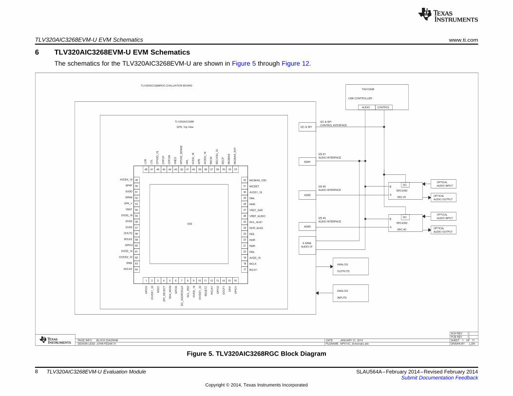
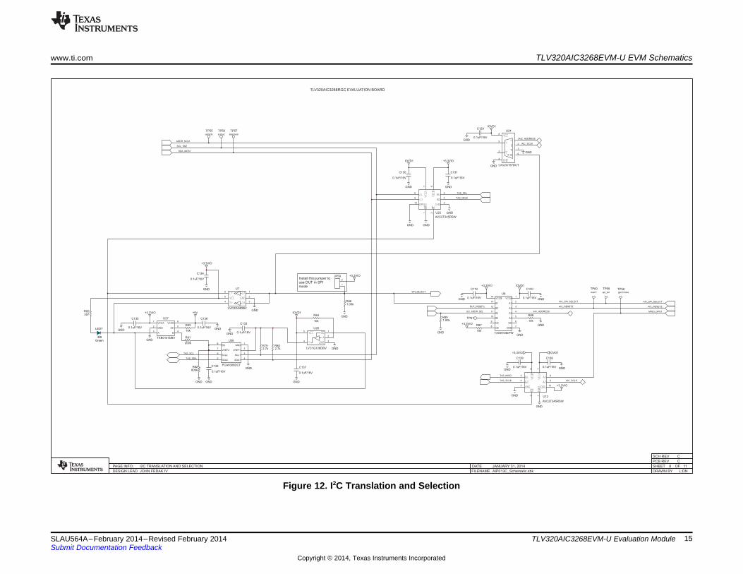
6 TLV320AIC3268EVM-U EVM SchematicsThe schematics for the TLV320AIC3268EVM-U are shown in Figure 5 through Figure 12.
Figure 5. TLV320AIC3268RGC Block Diagram
8 TLV320AIC3268EVM-U Evaluation Module SLAU564A–February 2014–Revised February 2014Submit Documentation Feedback
Copyright © 2014, Texas Instruments Incorporated

RESETz
TAS_MCLK
TAS_WCLK
TAS_MISO
TAS_MOSI
TAS_SSz
TAS_SCLK
I2S_ENABLE
TAS_SDA
TAS_BCLK
TAS_DIN
TAS_SCL
ASI_S0
ASI_S1
I2S3_DOUT_SRC
DUT_RESETz
TAS_DOUT
I2S2_DOUT_SRC
I2S1_DOUT
+5V
GNDGND GND
GND
GND
GND
GND
GND
GND
GND
GND
GND
GND
GND
GND
GND
GND
GND
GND
GND GND
GND
GND
GND
1.50k
R1
27.4
R2
27.4
R3
47pF/50V
C1
47pF/50V
C2
100kR4
1.0uF/16V
C321
S4
0.1uF/16V
C4
0.1uF/16V
C5
LVC1G126DBVR
VCCOE
A
GND
1
2
4
5
3
U30.1uF/16V
C7
0.1uF/16V
C8
1 2S1
0.1uF/50V
C9
10kR5
10kR6
21S2
0.1uF/16V
C10
0.1uF/50V
C11
1 2S3
10kR7
LED1
Yellow
649R8
LED2
Yellow
649R9
10kR10
21
EE Program
JP2
0.1uF/16V
C13
R11
3.09k
1000pF/50V
C14
100pF/50V
C15
10kR12
2.7kR13
2.7kR14
1
2
JP3
0.1uF/50V
C16
10kR15
4.7kR16
1
JP12
GND
4.7kR17
L;DN
11
C
C
JOHN FEDAK IV
JANUARY 31, 2014
AIP013C_Schematic.sbkDESIGN LEAD
PAGE INFO:
FILENAME
DATE OF
DRAWN BY
SHEET
PCB REV
SCH REV
+3.3VIO
+3.3VIO
+3.3VIO +3.3VIO
+3.3VIO
+3.3VIO
+3.3VIO
FB5
220ohms/2A
FB6
220ohms/2A
1
2
3
4
5
J1
Data+
GND
ID_NC
5v
Data-
+3.3VIO
1
2 3
4Y1
6.0MHz
Vcc
OUT
OE
GND
+3.3VIO
GND
C6
0.1uF/16V
+3.3VIO
GND
U5
PowerPAD24FC512-I/MF
GND
GND
C12
0.1uF/16V
+3.3VIO
+3.3VIO
+3.3VIO
U4
CBTLV3253DBQ
1
2
3
4
5
6
7 10
11
12
13
14
15
16
24FC512-I/MF
1
2
3
4 5
6
7
8U5
GND
+3.3VIO
GND
TAS1020BPFB
U2
(ADC Data)
7
8
9
10
11
12
6
5
4
3
2
1
25
26
27
28
29
30
31
32
33
34
35
36
TAS1020B USB HOST ADAPTER
TLV320AIC3268RGC EVALUATION BOARD
USB CONTROLLER 2
(DAC Data)
DUT RESET
APP
PATCH
USB RESET
USB INPUT
13 14 15 16 17 18 19 20 21 22 23 2413 14 15 16 17 18 19 20 21 22 23 24
373839404142434445464748
8 9
Y
TI
www.ti.com TLV320AIC3268EVM-U EVM Schematics
Figure 6. TAS1020BPFB USB Controller
9SLAU564A–February 2014–Revised February 2014 TLV320AIC3268EVM-U Evaluation ModuleSubmit Documentation Feedback
Copyright © 2014, Texas Instruments Incorporated

SRC1_RXCXO
SRC2_MCLK
SRC1_RDYz
TAS_SCL
TAS_SDA
RESETz
SRC1_MCLK
WCLK2
BCLK2
DIN2
SRC1_LOCKz
I2S2_DOUT_SRC
SRC2_RXCXO
SRC1_MCLK
SRC2_RDYz
SRC2_MCLK
DOUT3
WCLK3
BCLK3
DIN3
SRC2_LOCKz
TAS_DIN
TAS_WCLK
TAS_BCLK
DOUT2
WCLK1
BCLK1
DOUT1
DIN1I2S1_DOUT
I2S3_DOUT_SRC
GND
GNDGND
GNDGND
GND
GND GND GND
GND
GND
GND
GNDGND
GND
GND
GND GND
GND
GNDGND
GNDGND
GND
GND GND
GND
GND
GND
GNDGND
GND
GND
GND GND
C17
0.1uF/16V
C18
0.1uF/16V
C19
10uF/6.3V
C20
0.1uF/16V
C21
10uF/6.3V
C22
0.1uF/16V
C23
0.1uF/16V
C24
10uF/6.3V
C25
0.1uF/16V
C26
0.1uF/16V
C27
0.1uF/16V
C28
0.1uF/16V
R18
10k
R19
0
R20
0
C29
0.1uF/16V
C30
0.1uF/16V
C31
10uF/6.3V
C32
0.1uF/16V
C33
10uF/6.3V
C34
0.1uF/16V
C35
0.1uF/16V
C36
10uF/6.3V
C37
0.1uF/16V
C38
0.1uF/16V
C39
0.1uF/16V
C40
0.1uF/16V
R21
10k
R22
0
R230
R24
4.7k
R25
10k
R26
4.7k
C41
10uF/6.3V
C42
10uF/6.3V
1.00k
R27
1.00k
R28
GND
GND GND
C43
0.1uF/16V
C44
0.1uF/16V
R29
10k
L;DN
11
C
C
JOHN FEDAK IV
JANUARY 31, 2014
AIP013C_Schematic.sbkDESIGN LEAD
PAGE INFO:
FILENAME
DATE OF
DRAWN BY
SHEET
PCB REV
SCH REV
+3.3VIO
+3.3VIO
+3.3VIO
+3.3VIO
+3.3VIO
+3.3VIO
+3.3VIO
+3.3VIO
+3.3VIO
+3.3VIO
+3.3VIO
+3.3VIO
+3.3VIO
+3.3VIO
+3.3VIO
+3.3VIO
+3.3VIO
GND
SPDIF-OUT12
1
3
PLT133/T10W
SHIELD
GND
INPUT
VCC
1
2
3
SPDIF-IN1
PLR135/T10
Case
GND
VCC
OUT
GND
SPDIF-IN2
3
2
1
PLR135/T10
Case
GND
VCC
OUT
GND
GND
3
1
2SPDIF-OUT2
PLT133/T10W
SHIELD
GND
INPUT
VCC
IOVD1
+1.8VIO
IOVD2
+1.8VIO
IOVD1
+3.3VIO
1
2
3
4
5
6
78
9
10
11
12
13
14
TXS0104EPWR
U13
B4
NC
OE
NC
A4
B3
B2
B1
VCCB
A1
A2
A3
VCCA14
13
12
11
10
9
8 7
6
5
4
3
2
1U9
TXS0104EPWR
B4
NC
OE
NC
A4
B3
B2
B1
VCCB
A1
A2
A3
VCCA
1
2
3
4
5
6
78
9
10
11
12
13
14U14
TXS0104EPWR
B4
NC
OE
NC
A4
B3
B2
B1
VCCB
A1
A2
A3
VCCA
(DAC Data)
U6
Connect Pin44 to Pin10,pin 10 to ground plane
SRC #1
SRC4392IPFBR
i2c: 1110 000
13
1
2
3
4
5
6
7
8
9
10
11
12
14
15
16
17
18
19
20
21
22
23
24
25
26
27
28
29
30
31
32
33
34
35
36
37
38
39
40
41
42
43
44
45
46
47
48
U10
Connect Pin44 to Pin10,pin 10 to ground plane
SRC4392IPFBR
SRC #2
i2c: 1110 001
48
47
46
45
44
43
42
41
40
39
38
37
36
35
34
33
32
31
30
29
28
27
26
25
24
23
22
21
20
19
18
17
16
15
14
12
11
10
9
8
7
6
5
4
3
2
1
13
TLV320AIC3268RGC EVALUATION BOARD
3
DATA, SAMPLE RATE CONVERTER
Use same IOVD for IOVD1 and IOVD2.
BCLK3 -> GPIO2 (IOVD1)
WCLK3 -> GPIO1 (IOVD1)
DIN3 -> GPIO3 (IOVD2)
DOUT3 -> GPIO4 (IOVD2)
SAMPLE RATE CONVERTERS FOR ASIsTI
GND
GNDGND
TLV320AIC3268EVM-U EVM Schematics www.ti.com
Figure 7. Sample Rate Converters for ASIs
10 TLV320AIC3268EVM-U Evaluation Module SLAU564A–February 2014–Revised February 2014Submit Documentation Feedback
Copyright © 2014, Texas Instruments Incorporated

SRC1_LOCKz
SRC1_RDYz
SRC2_LOCKz
SRC2_RDYz
CLK2_DIV_S1
SRC2_MCLK_S0
CLK1_DIV_S0
CLK1_DIV_S1
SRC1_MCLK_S0
SRC1_MCLK
SRC2_MCLK
TAS_MCLK
MCLK_S0
MCLK_S1
MCLK_SEL
SRC2_MCLK_S1
SRC1_MCLK_S1
MCLK
SRC1_RXCXO
SRC2_RXCXO
SRC2_MCLK
SRC1_MCLK
TAS_SCL
TAS_SDA
RESETz
CLK1_DIV_S0
CLK1_DIV_S1
CLK2_DIV_S0
CLK2_DIV_S1
MCLK_S0
MCLK_S1
MCLK_SEL
SPI_SELECT
6Wire1_EN
I2C_ADDR_SEL
TAS_MCLK
ASI_S0
ASI_S1
SRC1_MCLK_S0
SRC1_MCLK_S1
SRC2_MCLK_S0
SRC2_MCLK_S1
CLK2_DIV_S0
GND
GND GND
GND
GND
GND
GND
GND
GND
GND
GND
GND
GND
GND
GND GND
GND
GND
GND
GND GNDGND
GND
GND
GND
GND
GND
R30
357
LED6
Green
R31
357
LED3
Green
R32
357
LED4
Green
R33
357
LED5
Green
C45
0.1uF/16V
R34
10k
R35
10k
R36
10k
C46
0.1uF/16V
C47
0.1uF/16V
R37
10k
R38
10k
R39
10k
C48
0.1uF16V
C49
0.1uF/16V
R4010k
R4110k
C50
0.1uF/16V
1
2
3
4
5
6
7
8 9
10
11
12
13
14
15
16U19
CBTLV3253DBQ
16
15
14
13
12
11
10
98
7
6
5
4
3
2
1U20
CBTLV3253DBQ
R4210k
R4310k
R44
10k
R4510k
GND
R4610k
C51
0.1uF/16V
GND
C52
0.1uF/16V
C53
0.1uF/16V
GND
GND
SPI_SELECT is only information,
Never drive this pin.Use Jumper JP51 instead
L;DN
11
C
C
JOHN FEDAK IV
JANUARY 31, 2014
AIP013C_Schematic.sbkDESIGN LEAD
PAGE INFO:
FILENAME
DATE OF
DRAWN BY
SHEET
PCB REV
SCH REV
TI
+3.3VIO
+3.3VIO+3.3VIO
+3.3VIO
+3.3VIO
+3.3VIO
+3.3VIO
+3.3VIO
+3.3VIO
+3.3VIO
+3.3VIO
+3.3VIO
+3.3VIO
+3.3VIO
+3.3VIO
+3.3VIO
IOVD1
+3.3VIO
8
7
6
54
3
2
1U17
ICS542MLFT
S1
OE
CLK/2
CLKICLK
VDD
GND
S0
24.576MHz
1
2 3
4OSC1
Vcc
OUT
OE
GND
22.5792MHz
1
2 3
4OSC2
Vcc
OUT
OE
GND
ICS542MLFT
1
2
3
4 5
6
7
8U18
S1
OE
CLK/2
CLKICLK
VDD
GND
S0
i2c: 1110 100
24
23
22
21
20
19
18
17
16
15
14
13
12
11
10
9
8
7
6
5
4
3
2
1
U22
TCA9539PW
1
2
3 4
5
6U15
LVC2G17DBV
2A
GND
1A6
5
43
2
1U16
LVC2G17DBV
2A
GND
1A
16
15
14
13
12
11
10
98
7
6
5
4
3
2
1U21
8
7
6
5
4
3
2
1
U11
+3.3VIO
TLV320AIC3268RGC EVALUATION BOARDCLOCKSDATA
4BOARD GPIO & MCLK FOR AIC3268
VCC
2Y
1Y
VCC
2Y
1Y
www.ti.com TLV320AIC3268EVM-U EVM Schematics
Figure 8. GPIO and MCLK for AIC3268
11SLAU564A–February 2014–Revised February 2014 TLV320AIC3268EVM-U Evaluation ModuleSubmit Documentation Feedback
Copyright © 2014, Texas Instruments Incorporated

AV_ENABLE
DV_ENABLE
AV_ENABLE
DV_ENABLE
DV_ENABLE
AV_ENABLE
BCLK1_DUT
WCLK1_DUT
DIN1_DUT
DOUT1_DUT
BCLK1
WCLK1
DIN1
DOUT1
MCLK_DUT
MCLK
BCLK2
WCLK2
DIN2
DOUT2
DOUT2_DUT
DIN2_DUT
WCLK2_DUT
BCLK2_DUT
TEST1
BCLK3
WCLK3
DIN3
DOUT3
GPIO1
GPIO2
GPIO3
GPIO3
GPIO4
GPIO4
TAS_WCLK
TAS_BCLK
6Wire1_EN
GPIO5
TEST2
+5V
GNDGND GND
+5V
GNDGND GND
+5V
GNDGND GND
+5V
GNDGND GND
+5V
GND
GNDGND GND
+5V
GNDGND GND
GND
0.1uF/16V
C54
10uF/6.3V
C55
10k
R47
0.1uF/16V
C56
10uF/6.3V
C57
10k
R48
0.1uF/16V
C58
10uF/6.3V
C59
10k
R49
0.1uF/16V
C60
10uF/6.3V
C61
10k
R50
0.1uF/16V
C62
10uF/6.3V
C63
10k
R51
0.1uF/16V
C64
10uF/6.3V
C65
10k
R52
47ufd/6.3V
C66
47uF/6.3V
C67
47uF/6.3V
C68
47uF/6.3V
C69
47ufd/6.3V
C70
47uF/6.3V
C71
TP69
TP1
TP2
JP221
2
3
JP23
3
2
1
TP62 TP63 TP64 TP65 TP66 TP67 TP68
TP3
TP4
TP5
GND
GND
GND
GND
TP6
TP7 TP8 TP9 TP10
GND
JP4
1 2 3
JP8
321
JP7
1 2 3
JP6
1 2 3
JP5
1 2 3
JP12
321
JP11
1 2 3
JP10
1 2 3
JP9
321
TP11TP12TP13TP14
GND
GND
GND
GND
DNP
J21 2
3 4
5 6
GND
TP15TP16
GND
0
R53
0
R54
GND
GND
GND
GND
JP13
1 2 3
JP14
321
JP15
321
JP16
1 2 3
gpio1/bclk3
TP17gpio2/wclk3
TP18gpio3/din3
TP19gpio4/dout3
TP20
JP20
1 2 3
JP21
3 2 1
GND GND
GND
GNDGND
0.1uF/16V
C72
0.1uF/16V
C73
10kR55
GND
DATACLOCK
SELECTVDD
MIC3
1
2
3
4
5
6
GND
GNDGND
GNDGNDGND
GND
0.1uF/16V
C91
0.1uF/16V
C90
SELECTCLOCKDATA
VDD
MIC2
6
5
4
3
2
1
JP19
3 2 1
JP18
123
JP17
3 2 1
GND GND GND
GND
GNDGND
GNDGNDGND
GND
0.1uF/16V
C74
0.1uF/16V
C75
DATACLOCK
SELECTVDD
MIC5
6
5
4
3
2
1
DATACLOCK
VDDSELECT
MIC4
1
2
3
4
5
6
L;DN
11
C
C
JOHN FEDAK IV
JANUARY 31, 2014
AIP013C_Schematic.sbkDESIGN LEAD
PAGE INFO:
FILENAME
DATE OF
DRAWN BY
SHEET
PCB REV
SCH REV
+1.8VA
+1.8VD
+3.3VA
+1.8V_CP
+3.3VIO
+3.3VIO
+3.3VIO+1.8VIO
+1.8VIO
+3.3VIO
IOVD2
IOVD1
IOVD2
GND
GND
GND
GND
GND
IOVD1
IOVD1
+1.8VIO
1.8V/400mA
VR31
2
3 4
5
TPS73618DBV
3.3V/400mA
VR51
2
3 4
5
TPS73633DBV
1.8V/400mA
VR15
43
2
1
TPS73618DBV
1.8V/400mA
VR21
2
3 4
5
TPS73618DBV
1.8V/400mA
VR41
2
3 4
5
TPS73618DBV
3.3V/400mA
VR65
43
2
1
TPS73633DBV
DNP
J3
SLIMbusSATA
7
6
5
4
3
2
1
GND
B+
B-
GND
A+
GND
A-
Case
U23
87654 3 2 1
TXB0102DCU
B2
A2
VC
CA
GN
D
B1
VC
CB
OE
A1
TLV320AIC3268RGC EVALUATION BOARD
LDOs & AIC3268 ANALOG OUTPUTS 5
LDO SUPPLIES
IOVD1: GPIO1: Dig_Mic 1,2 Data and BCLK3GPIO2: ADC_MOD_CLK and WCLK3
GPIO5: Dig_Mic 3,4 DataIOVD2: GPIO3: DIN3
GPIO4: DOUT3
Use same IOVD for IOVD1 and IOVD2.BCLK3 -> GPIO2 (IOVD1)WCLK3 -> GPIO1 (IOVD1)
DIN3 -> GPIO3 (IOVD2)DOUT3 -> GPIO4 (IOVD2)
TI
TLV320AIC3268EVM-U EVM Schematics www.ti.com
Figure 9. LDO Supplies and Analog Outputs
12 TLV320AIC3268EVM-U Evaluation Module SLAU564A–February 2014–Revised February 2014Submit Documentation Feedback
Copyright © 2014, Texas Instruments Incorporated

VSYS_EXT
HS_MIC
MICBIAS_EXT
IN4R
IN4L
MICBIAS_DUT MICBIAS
BCLK1_DUT
MCLK_DUT
IN2L
IN2R
IN3L
IN3R
VSYS_EXT
MICBIAS_EXT_DUT
MICBIAS_DUT
MICBIAS_EXT_DUT
IN1R
IN1L
VSYS_EXT
SPKM
SPKP
RECP
RECM
HPR
HPL
HPVSS_SENSE
RLOUT
LLOUT
GPIO1
DIN1_DUT
DOUT1_DUT
GPIO2
WCLK1_DUT
AIC_RESETZ
SCL_SSZ
ADDR_SCLK
GPIO5
SDA_MOSI
AIC_SPI_SELECT
MISO_GPO1
GPIO3
WC
LK
2_D
UT
DIN
2_D
UT
GP
IO4
BC
LK
2_D
UT
DO
UT
2_D
UT
TE
ST
1
TE
ST
2
GND
JP32
1
2
JP39
1
2
GND
JP37
3 2 1
GND
JP45
2 1
GND
GND GND
JP25
1 2
GND GND
JP48
21
JP24
1 2
+1.8VIO
JP47
321
TP21
vref
GND
TP22micdet
JP35
1
2
JP33
1 2 3
GND
TP23Ext_Aux1
TP24Ext_Aux2
0.1uF/16V
C76
0.1uF/16V
C77
0.1uF/16V
C78
0.1uF/16V
C79
0.1uF/16V
C80
1.0uF/16V
C81
0.1uF/16V
C83
10uF/10V
C84
C85
1.0uF/16VC86
1.0uF/16V
0.1uF/16V
C87
R56
200
R57
200
JP36
2
1
100
R58
R592.10k
TP25
in1l
JP34
321
0.1uF/16V
C88
GND
TP26
in1r
TP27Ext_In1R
C89
1.0uF/16V
TP28in4l
TP29in4r
CP90
1.0ufd/10V
CP91
1.0ufd/10V
GND
MIC11
2
JP31
2
1
R601.10k
TP30
100
R61
R621.00k
R632.10k
JP27
1 2
R642.10k
JP28
21
TP31in3l
TP32in3r
C92
1.0uF/16V
C93
1.0uF/16V
JP30
1 2
JP29
2 1
GNDTP33
in2r
TP34
in2l
C94
1.0uF/10V
C95
1.0uF/16V
GNDGND
1.0uF/16V
C96
0.1uF/16V
C97
JP26
21
1.0uF/16V
C98
GND
TP35vref_sar
R65200
0.1uF/16V
C99
GND
JP462
1
TP36
C100
2.2ufd/10V
GND
C101
2.2uF/10V
TP37Vneg
GND GND
0.1uF/16V
C102
10uF/10V
C103
GND
10uF/10V
C104
GND
0.1uF/16V
C105
JP40
123
JP41
2 1
GND GND
GND
GND
DNP
C106
DNP
C107
JP42 2
1
R66
1.00k
2200pfd/50V
C108
JP431
2R67
1.00K
2200pfd/50V
C109
TP38 TP39
120 OHMS/1.5A
FB1
21
1
120 OHMS/1.5A
FB22
6A/125V
J5
1
2
+
1.0uF/16V
C110
6A/125V
J6
2
1+
JP44
1 2 3
GND GND GND
GND
+5V
TP40spkm
TP41spkp
10uF/10V
C111
0.1uF/16V
C112
JP38
321
0.1uF/16V
C113
1.0uF/16V
C114
GND GND
GND GND
1.0uF/16V
C116
GND
0.1uF/16V
C117
GND
10uF/10V
C118
PowerPAD
U1
GND
0.1uF/16V
C115
L;DN
11
C
C
JOHN FEDAK IV
JANUARY 31, 2014
AIP013C_Schematic.sbkDESIGN LEAD
PAGE INFO:
FILENAME
DATE OF
DRAWN BY
SHEET
PCB REV
SCH REV
TI
+1.8VD
IOVD1
+1.8VA
+1.8VA
+1.8VD
+1.8V_CP
+1.8VA
+1.8VA
+1.8VA +3.3VA
+3.3VA
+1.8VA
FB4
220ohms/2A
2 1
U1
64 60 56 52
45
41
37
33
54 5355 51 495058 5759
44
43
42
46
47
48
40
39
38
25 26 2827 31 32302921 22 242319 2018
9
10
11
12
16
15
14
13
5
6
7
8
63 6162
17
34
35
36
4
3
2
1
GND
C140
0.1uF/16V
IOVD2
J4
LEFT
RIGHT
Sh
ield
2
4
1
3
6
5
TLV320AIC3268RGC EVALUATION BOARD
TLV320AIC3268 6
www.ti.com TLV320AIC3268EVM-U EVM Schematics
Figure 10. TLV320AIC3268 Schematic
13SLAU564A–February 2014–Revised February 2014 TLV320AIC3268EVM-U Evaluation ModuleSubmit Documentation Feedback
Copyright © 2014, Texas Instruments Incorporated

HS_MIC
HPVSS_SENSE
HPL
HPL
HPR
HPR
RECP
RECP
RECM
RECM
LLOUT
LLOUT
RLOUT
RLOUT
hpl
TP42
hpr
TP43
vss_sns
TP44
GNDGND
GND
GNDGNDGND
GND
123
JP52
3 2 1
JP53
321
JP50
321
JP51
R68
1.00k R69
1.00k
16.0R70
32.4R71
16.0R90
2200pF/50V
C1212200pF/50V
C122
32.4R72
TP45
TP46
GND
2 1
JP49
DNP
R73
GND
GNDGND
1.0ufF16V
C123
1.0uF/16V
C124
llout
TP47
rlout
TP48
1 2
JP57
TP49
21
JP58
TP50R74
1.00k
2200pF/50V
C125
R75
1.00k
2200pF/50V
C126
GND
GND GND
21
JP54
R76
1.00k
2200pF/50V
C127
1 2
JP55
R77
1.00k
2200pF/50V
C128
TP51 TP52
32.4
R781
2
JP56recp
TP53
recm
TP54
L;DN
11
C
C
JOHN FEDAK IV
JANUARY 31, 2014
AIP013C_Schematic.sbkDESIGN LEAD
PAGE INFO:
FILENAME
DATE OF
DRAWN BY
SHEET
PCB REV
SCH REV
TI
J9
1
2
3
6A/125V
220ohms/2A
1 2FB3
J8
3
2
1
4
5
Sh
ield
J7
LEFT
RIGHT
Sh
ield
2
4
1
3
6
5
J10
LEFT
RIGHT
Shie
ld
2
4
1
3
6
5
TLV320AIC3268RGC EVALUATION BOARD
AUDIO CONNECTORS 7
2-32-3
1-21-2
JP51JP50Configuration
L-R-G-M
L-R-M-G
TLV320AIC3268EVM-U EVM Schematics www.ti.com
Figure 11. Audio Connectors
14 TLV320AIC3268EVM-U Evaluation Module SLAU564A–February 2014–Revised February 2014Submit Documentation Feedback
Copyright © 2014, Texas Instruments Incorporated
SCL_SSZ
SDA_MOSI
AIC_SCLK
AIC_ADDRESSADDR_SCLK
TAS_SSz
TAS_MOSI
TAS_SCL
TAS_SDA
DUT_RESETz AIC_RESETZAIC_RESETZ
TAS_SCLK
TAS_MISO
I2C_ADDR_SEL AIC_ADDRESS
AIC_SPI_SELECTAIC_SPI_SELECT
AIC_SCLK
SPI_SELECT
MISO_GPO1
ad/sclk
TP55scl/ssz
TP56sda/mosi
TP57
gpo1/miso
TP58spi_sel
TP59reset~
TP60
GND
GND0.1uF/16V
C129
GND
GND GND
GND
GND GND
0.1uF/16V
C130
0.1uF/16V
C131
GND
GND
GNDGND
GND
GND
+5V
GND
GND GND
GND
GND
0.1uF/16V
C132
2.7kR79
2.7kR80
0.1uF/16V
C133
200k
R81
R82806k
0.1uF/16V
C134
10k
R830.1uF/16V
C135
0.1uF/16V
C13610k
R84
0.1uF/16V
C137
GND
1
JP592
357R85
Green
LED7
R861.00k
GND
GND
GNDGND0.1uF/16V
C138
0.1uF/16V
C139
GND
GND GND0.1uF/16V
C119
0.1uF/16V
C120
10k
R87
GND
10k
R88
GND
TP61R891.00k
L;DN
11
C
C
JOHN FEDAK IV
JANUARY 31, 2014
AIP013C_Schematic.sbkDESIGN LEAD
PAGE INFO:
FILENAME
DATE OF
DRAWN BY
SHEET
PCB REV
SCH REV
TI
IOVD1
+3.3VIO
+3.3VIO
+3.3VIO
+3.3VIO
+3.3VIO IOVD1
IOVD1+3.3VIO
+3.3VIO
IOVD1
IOVD1 +3.3VIO
1
2
3
4
5
6
7
8
U24
LVC2G157DCT
10
9
8
7 6
5
4
3
21 U25
AVC2T245RSW
1
2
3
45
6
7
8
U26
PCA9306DCT
SDA2
SCL2
VREF2
EN
SDA1
GND
VREF1
SCL1
1
2
3 4
5
6
U27
TXB0101DBV
OE
VCCB
B
GND
VCCA
A1
2
4
5
3
U28
LVC1G126DBV
1
2
34
5
6
U7
LVC2G04DBV
14
13
12
11
10
9
8 7
6
5
4
3
2
1
U8
TXS0104EPW
B4
NC
OE GND
NC
A4
B3
B2
B1
VCCB
A1
A2
A3
VCCA
U1212
3
4
5
6 7
8
9
10
AVC2T245RSW
TLV320AIC3268RGC EVALUATION BOARD
I2C TRANSLATION AND SELECTION 8
Install this jumper touse DUT in SPImode
www.ti.com TLV320AIC3268EVM-U EVM Schematics
Figure 12. I2C Translation and Selection
15SLAU564A–February 2014–Revised February 2014 TLV320AIC3268EVM-U Evaluation ModuleSubmit Documentation Feedback
Copyright © 2014, Texas Instruments Incorporated

DV_ENABLE
TAS_SCL
TAS_SDA
MCLK
BCLK1
WCLK1
DOUT1
DIN1
TAS_MISO
TAS_MOSI
TAS_SSz
TAS_SCLK
I2S_ENABLE
RESETz
BCLK2
WCLK2
DOUT2
DIN2
BCLK2
WCLK2
DOUT2
DIN2
TAS_BCLK
TAS_WCLK
TAS_DOUT
TAS_DIN
GPIO3
GPIO4
IN1L IN1R
IN2L IN2R
IN3RIN3L
IN4L IN4R
MICBIAS
MICBIAS_EXT HS_MIC
SPKP
SPKM SPKM
SPKP
RECP RECM
LLOUT
RLOUT
HPL
HPR
AV_ENABLE
GPIO5
GPIO1
GPIO2
GND GND
VARVDVARVD
70
68
66
64
62
60
58
56
54
52
50
48
46
44
42
40
38
36
34
32
30
28
26
24
22
20
18
16
14
12
10
8
6
4
2
69
67
65
63
61
59
57
55
53
51
49
47
45
43
41
39
37
35
33
31
29
27
25
23
21
19
17
15
13
11
9
7
5
3
1
71
73
75
77
79
81
83
85
87
89
91
93
95
97
99
72
74
76
78
80
82
84
86
88
90
92
94
96
98
100
J11
mfg: JSTp/n: 100P-JMDSS-G-1-TF(LF)(SN)
100
98
96
94
92
90
88
86
84
76
74
72
70
68
66
64
62
60
58
56
54
52
50
48
46
44
42
40
38
36
34
32
30
28
26
24
22
20
18
16
14
12
10
8
6
4
2
99
97
95
93
91
89
87
85
83
73
71
69
67
65
63
61
59
57
55
53
51
49
47
45
43
41
39
37
35
33
31
29
27
25
23
21
19
17
15
13
11
9
7
5
3
1
75
77
79
81
78
80
82
J12
mfg: JSTp/n: 100P-JMDSS-G-1-TF(LF)(SN)
S03
0.5in0.5in
S02
0.5in0.5in
S05
0.5in0.5in
S04
0.5in0.5in
S07
0.5in0.5in
S01
0.5in0.5in
S06
0.5in0.5in
S08
0.5in0.5in
L;DN
11
C
C
JOHN FEDAK IV
JANUARY 31, 2014
AIP013C_Schematic.sbkDESIGN LEAD
PAGE INFO:
FILENAME
DATE OF
DRAWN BY
SHEET
PCB REV
SCH REV
TI
GND GND
+1.8V_CP +3.3VD
GND GND
+5V +5V
+1.8V +1.8V
+3.3VD +3.3VDGND
J12
Anchor
J11
Anchor
TLV320AIC3268RGC EVALUATION BOARD
9
RESERVED
RESERVED
I2S_4
I2S_3
GPIO
DGND
I2S_ENABLE
DGND
I2S1
DGND
MCLK
I2C
RESERVEDRESERVED
DV_ENABLE
VARVD VARVD
+1.8VD +1.8IO
+3.3IO +3.0IO
DGND
DGND
DGND
DGND
DGND
DGND
DGND
DGND+5VD+5VD
IN8-
IN7-
IN6-
IN5-
IN4-
IN3-
IN1-
IN2-
MICDETAGND
AGND
AGND
AGND
AGND
AGND
AGND
AGND
IN8+
IN7+
IN6+
IN5+
IN4+
IN3+
IN1+
IN2+
MICBIASAGND
AGND
AGND
AGND
AGND
AGND
AGND
AGND
AGND AGNDSPK1+SPK1-SPK2+SPK2-
CLASS-DSPEAKEROUTPUT
CLASS-DSPEAKEROUTPUT
SPK2-SPK2+SPK1-SPK1+
HEADSETGROUND
HPGNDHPGND
HPGNDHPGND
LINEOUTPUTS
OUT1GNDOUT1+
OUT2+OUT2GND
OUT3+OUT3GND
OUT4GNDOUT4+
AGND
HP2LHP2R
HP1R
OUT4-OUT4GND
HP1LHEADSETOUTPUTS
AGND
OUT3GNDOUT3-OUT2GNDOUT2-
OUT1-OUT1GND
LINEOUTPUTS
AGNDVARVA
BREAK-OUT CONNECTIONSBREAK-OUT CONNECTIONS
ANALOG INTERFACE CONNECTOR
STANDOFFS
+5VAAGND
+3.3VA
AGND+1.8V_CP
AGND
VARVAAGND
AGND+1.8VAAGND
+3.3VAAGND+5VA
BREAK-OUT CONNECTIONSBREAK-OUT CONNECTIONS
DIGITAL INTERFACE CONNECTOR
AV_ENABLEHPVDDHPGND
RESERVED
HPGNDHPVDD
SPKVDD SPKVDD
SPKGND SPKGND RESERVED
MCLK
SPI
RESET
I2S_2
RESERVED
BREAKOUT BOARD CONNECTIONS
TLV320AIC3268EVM-U EVM Schematics www.ti.com
Figure 13. Breakout Board Connections
16 TLV320AIC3268EVM-U Evaluation Module SLAU564A–February 2014–Revised February 2014Submit Documentation Feedback
Copyright © 2014, Texas Instruments Incorporated

www.ti.com TLV320AIC3268EVM-U EVM Board Layout
7 TLV320AIC3268EVM-U EVM Board LayoutFigure 14 through Figure 16 illustrate the TLV320AIC3268EVM-U EVM board layouts.
Figure 14. Top Xray View
Figure 15. Silkscreen Top
17SLAU564A–February 2014–Revised February 2014 TLV320AIC3268EVM-U Evaluation ModuleSubmit Documentation Feedback
Copyright © 2014, Texas Instruments Incorporated

TLV320AIC3268EVM-U EVM Board Layout www.ti.com
Figure 16. Silkscreen Bottom
18 TLV320AIC3268EVM-U Evaluation Module SLAU564A–February 2014–Revised February 2014Submit Documentation Feedback
Copyright © 2014, Texas Instruments Incorporated
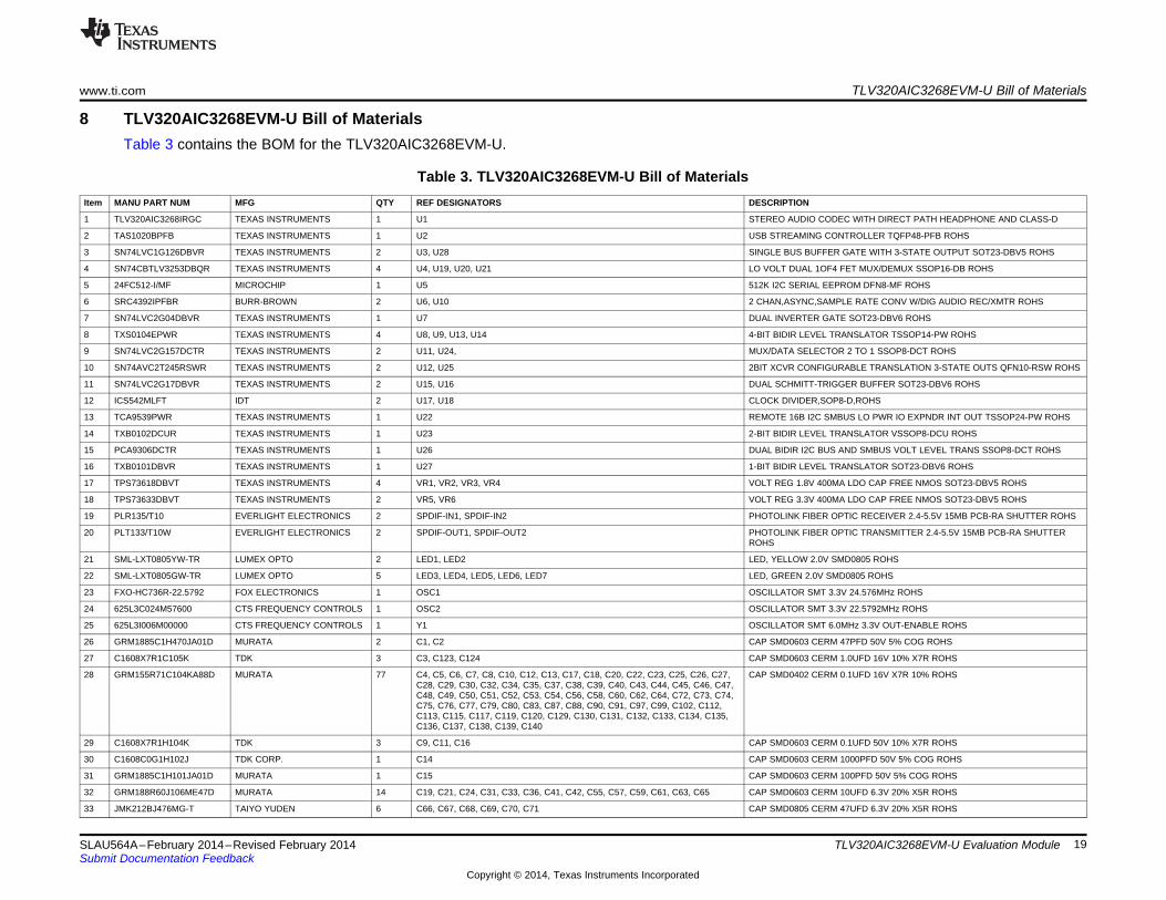
www.ti.com TLV320AIC3268EVM-U Bill of Materials
8 TLV320AIC3268EVM-U Bill of MaterialsTable 3 contains the BOM for the TLV320AIC3268EVM-U.
Table 3. TLV320AIC3268EVM-U Bill of MaterialsItem MANU PART NUM MFG QTY REF DESIGNATORS DESCRIPTION
1 TLV320AIC3268IRGC TEXAS INSTRUMENTS 1 U1 STEREO AUDIO CODEC WITH DIRECT PATH HEADPHONE AND CLASS-D
2 TAS1020BPFB TEXAS INSTRUMENTS 1 U2 USB STREAMING CONTROLLER TQFP48-PFB ROHS
3 SN74LVC1G126DBVR TEXAS INSTRUMENTS 2 U3, U28 SINGLE BUS BUFFER GATE WITH 3-STATE OUTPUT SOT23-DBV5 ROHS
4 SN74CBTLV3253DBQR TEXAS INSTRUMENTS 4 U4, U19, U20, U21 LO VOLT DUAL 1OF4 FET MUX/DEMUX SSOP16-DB ROHS
5 24FC512-I/MF MICROCHIP 1 U5 512K I2C SERIAL EEPROM DFN8-MF ROHS
6 SRC4392IPFBR BURR-BROWN 2 U6, U10 2 CHAN,ASYNC,SAMPLE RATE CONV W/DIG AUDIO REC/XMTR ROHS
7 SN74LVC2G04DBVR TEXAS INSTRUMENTS 1 U7 DUAL INVERTER GATE SOT23-DBV6 ROHS
8 TXS0104EPWR TEXAS INSTRUMENTS 4 U8, U9, U13, U14 4-BIT BIDIR LEVEL TRANSLATOR TSSOP14-PW ROHS
9 SN74LVC2G157DCTR TEXAS INSTRUMENTS 2 U11, U24, MUX/DATA SELECTOR 2 TO 1 SSOP8-DCT ROHS
10 SN74AVC2T245RSWR TEXAS INSTRUMENTS 2 U12, U25 2BIT XCVR CONFIGURABLE TRANSLATION 3-STATE OUTS QFN10-RSW ROHS
11 SN74LVC2G17DBVR TEXAS INSTRUMENTS 2 U15, U16 DUAL SCHMITT-TRIGGER BUFFER SOT23-DBV6 ROHS
12 ICS542MLFT IDT 2 U17, U18 CLOCK DIVIDER,SOP8-D,ROHS
13 TCA9539PWR TEXAS INSTRUMENTS 1 U22 REMOTE 16B I2C SMBUS LO PWR IO EXPNDR INT OUT TSSOP24-PW ROHS
14 TXB0102DCUR TEXAS INSTRUMENTS 1 U23 2-BIT BIDIR LEVEL TRANSLATOR VSSOP8-DCU ROHS
15 PCA9306DCTR TEXAS INSTRUMENTS 1 U26 DUAL BIDIR I2C BUS AND SMBUS VOLT LEVEL TRANS SSOP8-DCT ROHS
16 TXB0101DBVR TEXAS INSTRUMENTS 1 U27 1-BIT BIDIR LEVEL TRANSLATOR SOT23-DBV6 ROHS
17 TPS73618DBVT TEXAS INSTRUMENTS 4 VR1, VR2, VR3, VR4 VOLT REG 1.8V 400MA LDO CAP FREE NMOS SOT23-DBV5 ROHS
18 TPS73633DBVT TEXAS INSTRUMENTS 2 VR5, VR6 VOLT REG 3.3V 400MA LDO CAP FREE NMOS SOT23-DBV5 ROHS
19 PLR135/T10 EVERLIGHT ELECTRONICS 2 SPDIF-IN1, SPDIF-IN2 PHOTOLINK FIBER OPTIC RECEIVER 2.4-5.5V 15MB PCB-RA SHUTTER ROHS
20 PLT133/T10W EVERLIGHT ELECTRONICS 2 SPDIF-OUT1, SPDIF-OUT2 PHOTOLINK FIBER OPTIC TRANSMITTER 2.4-5.5V 15MB PCB-RA SHUTTERROHS
21 SML-LXT0805YW-TR LUMEX OPTO 2 LED1, LED2 LED, YELLOW 2.0V SMD0805 ROHS
22 SML-LXT0805GW-TR LUMEX OPTO 5 LED3, LED4, LED5, LED6, LED7 LED, GREEN 2.0V SMD0805 ROHS
23 FXO-HC736R-22.5792 FOX ELECTRONICS 1 OSC1 OSCILLATOR SMT 3.3V 24.576MHz ROHS
24 625L3C024M57600 CTS FREQUENCY CONTROLS 1 OSC2 OSCILLATOR SMT 3.3V 22.5792MHz ROHS
25 625L3I006M00000 CTS FREQUENCY CONTROLS 1 Y1 OSCILLATOR SMT 6.0MHz 3.3V OUT-ENABLE ROHS
26 GRM1885C1H470JA01D MURATA 2 C1, C2 CAP SMD0603 CERM 47PFD 50V 5% COG ROHS
27 C1608X7R1C105K TDK 3 C3, C123, C124 CAP SMD0603 CERM 1.0UFD 16V 10% X7R ROHS
28 GRM155R71C104KA88D MURATA 77 C4, C5, C6, C7, C8, C10, C12, C13, C17, C18, C20, C22, C23, C25, C26, C27, CAP SMD0402 CERM 0.1UFD 16V X7R 10% ROHSC28, C29, C30, C32, C34, C35, C37, C38, C39, C40, C43, C44, C45, C46, C47,C48, C49, C50, C51, C52, C53, C54, C56, C58, C60, C62, C64, C72, C73, C74,C75, C76, C77, C79, C80, C83, C87, C88, C90, C91, C97, C99, C102, C112,C113, C115, C117, C119, C120, C129, C130, C131, C132, C133, C134, C135,C136, C137, C138, C139, C140
29 C1608X7R1H104K TDK 3 C9, C11, C16 CAP SMD0603 CERM 0.1UFD 50V 10% X7R ROHS
30 C1608C0G1H102J TDK CORP. 1 C14 CAP SMD0603 CERM 1000PFD 50V 5% COG ROHS
31 GRM1885C1H101JA01D MURATA 1 C15 CAP SMD0603 CERM 100PFD 50V 5% COG ROHS
32 GRM188R60J106ME47D MURATA 14 C19, C21, C24, C31, C33, C36, C41, C42, C55, C57, C59, C61, C63, C65 CAP SMD0603 CERM 10UFD 6.3V 20% X5R ROHS
33 JMK212BJ476MG-T TAIYO YUDEN 6 C66, C67, C68, C69, C70, C71 CAP SMD0805 CERM 47UFD 6.3V 20% X5R ROHS
19SLAU564A–February 2014–Revised February 2014 TLV320AIC3268EVM-U Evaluation ModuleSubmit Documentation Feedback
Copyright © 2014, Texas Instruments Incorporated
TLV320AIC3268EVM-U Bill of Materials www.ti.com
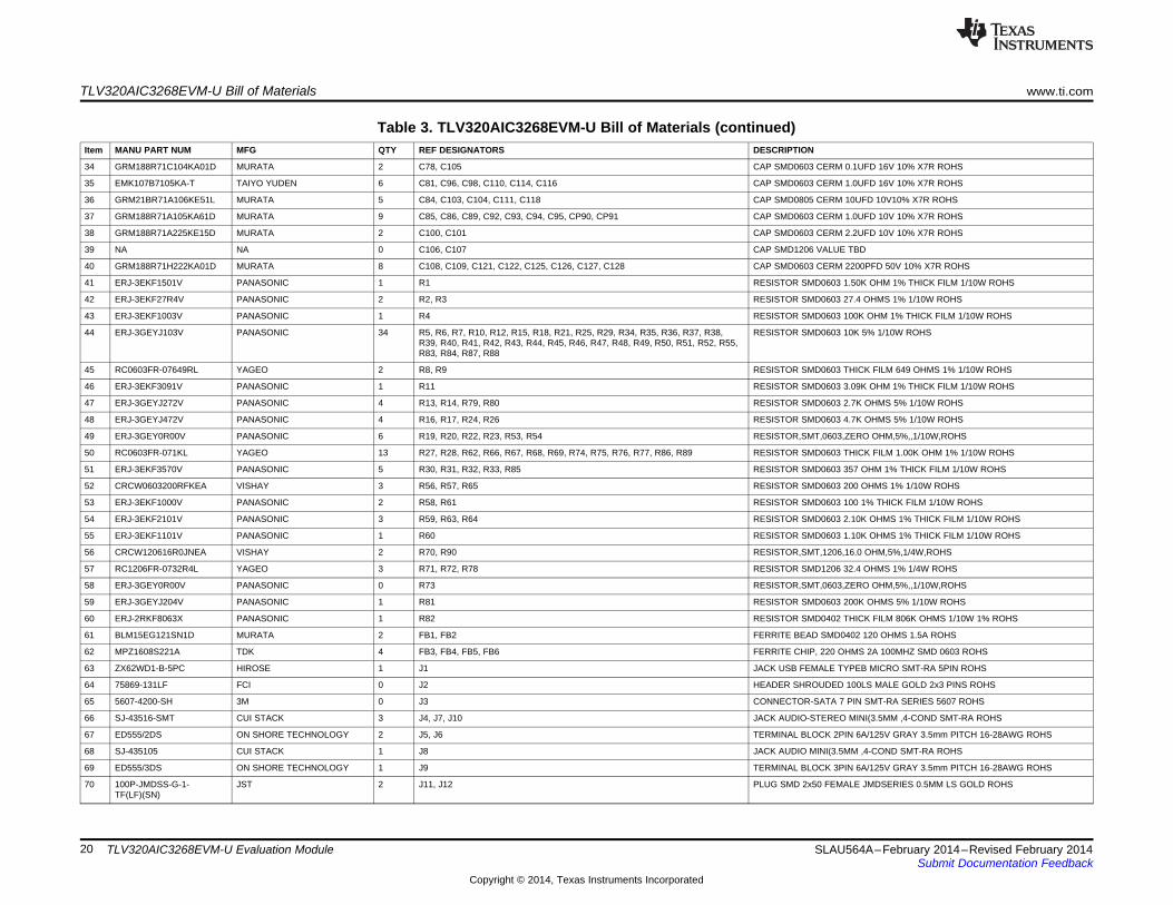
Table 3. TLV320AIC3268EVM-U Bill of Materials (continued)Item MANU PART NUM MFG QTY REF DESIGNATORS DESCRIPTION
34 GRM188R71C104KA01D MURATA 2 C78, C105 CAP SMD0603 CERM 0.1UFD 16V 10% X7R ROHS
35 EMK107B7105KA-T TAIYO YUDEN 6 C81, C96, C98, C110, C114, C116 CAP SMD0603 CERM 1.0UFD 16V 10% X7R ROHS
36 GRM21BR71A106KE51L MURATA 5 C84, C103, C104, C111, C118 CAP SMD0805 CERM 10UFD 10V10% X7R ROHS
37 GRM188R71A105KA61D MURATA 9 C85, C86, C89, C92, C93, C94, C95, CP90, CP91 CAP SMD0603 CERM 1.0UFD 10V 10% X7R ROHS
38 GRM188R71A225KE15D MURATA 2 C100, C101 CAP SMD0603 CERM 2.2UFD 10V 10% X7R ROHS
39 NA NA 0 C106, C107 CAP SMD1206 VALUE TBD
40 GRM188R71H222KA01D MURATA 8 C108, C109, C121, C122, C125, C126, C127, C128 CAP SMD0603 CERM 2200PFD 50V 10% X7R ROHS
41 ERJ-3EKF1501V PANASONIC 1 R1 RESISTOR SMD0603 1.50K OHM 1% THICK FILM 1/10W ROHS
42 ERJ-3EKF27R4V PANASONIC 2 R2, R3 RESISTOR SMD0603 27.4 OHMS 1% 1/10W ROHS
43 ERJ-3EKF1003V PANASONIC 1 R4 RESISTOR SMD0603 100K OHM 1% THICK FILM 1/10W ROHS
44 ERJ-3GEYJ103V PANASONIC 34 R5, R6, R7, R10, R12, R15, R18, R21, R25, R29, R34, R35, R36, R37, R38, RESISTOR SMD0603 10K 5% 1/10W ROHSR39, R40, R41, R42, R43, R44, R45, R46, R47, R48, R49, R50, R51, R52, R55,R83, R84, R87, R88
45 RC0603FR-07649RL YAGEO 2 R8, R9 RESISTOR SMD0603 THICK FILM 649 OHMS 1% 1/10W ROHS
46 ERJ-3EKF3091V PANASONIC 1 R11 RESISTOR SMD0603 3.09K OHM 1% THICK FILM 1/10W ROHS
47 ERJ-3GEYJ272V PANASONIC 4 R13, R14, R79, R80 RESISTOR SMD0603 2.7K OHMS 5% 1/10W ROHS
48 ERJ-3GEYJ472V PANASONIC 4 R16, R17, R24, R26 RESISTOR SMD0603 4.7K OHMS 5% 1/10W ROHS
49 ERJ-3GEY0R00V PANASONIC 6 R19, R20, R22, R23, R53, R54 RESISTOR,SMT,0603,ZERO OHM,5%,,1/10W,ROHS
50 RC0603FR-071KL YAGEO 13 R27, R28, R62, R66, R67, R68, R69, R74, R75, R76, R77, R86, R89 RESISTOR SMD0603 THICK FILM 1.00K OHM 1% 1/10W ROHS
51 ERJ-3EKF3570V PANASONIC 5 R30, R31, R32, R33, R85 RESISTOR SMD0603 357 OHM 1% THICK FILM 1/10W ROHS
52 CRCW0603200RFKEA VISHAY 3 R56, R57, R65 RESISTOR SMD0603 200 OHMS 1% 1/10W ROHS
53 ERJ-3EKF1000V PANASONIC 2 R58, R61 RESISTOR SMD0603 100 1% THICK FILM 1/10W ROHS
54 ERJ-3EKF2101V PANASONIC 3 R59, R63, R64 RESISTOR SMD0603 2.10K OHMS 1% THICK FILM 1/10W ROHS
55 ERJ-3EKF1101V PANASONIC 1 R60 RESISTOR SMD0603 1.10K OHMS 1% THICK FILM 1/10W ROHS
56 CRCW120616R0JNEA VISHAY 2 R70, R90 RESISTOR,SMT,1206,16.0 OHM,5%,1/4W,ROHS
57 RC1206FR-0732R4L YAGEO 3 R71, R72, R78 RESISTOR SMD1206 32.4 OHMS 1% 1/4W ROHS
58 ERJ-3GEY0R00V PANASONIC 0 R73 RESISTOR,SMT,0603,ZERO OHM,5%,,1/10W,ROHS
59 ERJ-3GEYJ204V PANASONIC 1 R81 RESISTOR SMD0603 200K OHMS 5% 1/10W ROHS
60 ERJ-2RKF8063X PANASONIC 1 R82 RESISTOR SMD0402 THICK FILM 806K OHMS 1/10W 1% ROHS
61 BLM15EG121SN1D MURATA 2 FB1, FB2 FERRITE BEAD SMD0402 120 OHMS 1.5A ROHS
62 MPZ1608S221A TDK 4 FB3, FB4, FB5, FB6 FERRITE CHIP, 220 OHMS 2A 100MHZ SMD 0603 ROHS
63 ZX62WD1-B-5PC HIROSE 1 J1 JACK USB FEMALE TYPEB MICRO SMT-RA 5PIN ROHS
64 75869-131LF FCI 0 J2 HEADER SHROUDED 100LS MALE GOLD 2x3 PINS ROHS
65 5607-4200-SH 3M 0 J3 CONNECTOR-SATA 7 PIN SMT-RA SERIES 5607 ROHS
66 SJ-43516-SMT CUI STACK 3 J4, J7, J10 JACK AUDIO-STEREO MINI(3.5MM ,4-COND SMT-RA ROHS
67 ED555/2DS ON SHORE TECHNOLOGY 2 J5, J6 TERMINAL BLOCK 2PIN 6A/125V GRAY 3.5mm PITCH 16-28AWG ROHS
68 SJ-435105 CUI STACK 1 J8 JACK AUDIO MINI(3.5MM ,4-COND SMT-RA ROHS
69 ED555/3DS ON SHORE TECHNOLOGY 1 J9 TERMINAL BLOCK 3PIN 6A/125V GRAY 3.5mm PITCH 16-28AWG ROHS
70 100P-JMDSS-G-1- JST 2 J11, J12 PLUG SMD 2x50 FEMALE JMDSERIES 0.5MM LS GOLD ROHSTF(LF)(SN)
20 TLV320AIC3268EVM-U Evaluation Module SLAU564A–February 2014–Revised February 2014Submit Documentation Feedback
Copyright © 2014, Texas Instruments Incorporated

www.ti.com TLV320AIC3268EVM-U Bill of Materials
Table 3. TLV320AIC3268EVM-U Bill of Materials (continued)Item MANU PART NUM MFG QTY REF DESIGNATORS DESCRIPTION
71 PBC02SAAN SULLINS 28 JP1, JP2, JP3, JP24, JP25, JP26, JP27, JP28, JP29, JP30, JP31, JP32, JP35, HEADER THRU MALE 2 PIN 100LS 120 TAIL GOLD ROHSJP36, JP39, JP41, JP42, JP43, JP45, JP46, JP48, JP49, JP54, JP55, JP56,JP57, JP58, JP59
72 PBC03SAAN SULLINS 31 JP4, JP5, JP6, JP7, JP8, JP9, JP10, JP11, JP12, JP13, JP14, JP15, JP16, JP17, HEADER THRU MALE 3 PIN 100LS 120 TAIL GOLD ROHSJP18, JP19, JP20, JP21, JP22, JP23, JP33, JP34, JP37, JP38, JP40, JP44,JP47, JP50, JP51, JP52, JP53
73 WM-63PRT PANASONIC 1 MIC1 MICROPHONE ELECTRET OMNIDIRECTIONAL DUAL BAND 2PIN ROHS
74 SPM0423HD4H-WB KNOWLES 4 MIC2, MIC3, MIC4, MIC5 MIC DIGITAL MIMI-SISONIC HALOGEN FREE 6PIN ROHS
75 5000 KEYSTONE ELECTRONICS 11 TP1, TP2, TP3, TP4, TP5, TP21, TP30, TP35, TP36, TP37, TP69 PC TESTPOINT, RED, ROHS
76 5002 KEYSTONE ELECTRONICS 30 TP22, TP23, TP24, TP25, TP26, TP27, TP28, TP29, TP31, TP32, TP33, TP34, PC TESTPOINT, WHITE, ROHSTP38, TP39, TP40, TP41, TP42, TP43, TP44, TP45, TP46, TP47, TP48, TP49,TP50, TP51, TP52, TP53, TP54, TP61
77 5004 KEYSTONE ELECTRONICS 21 TP6, TP7, TP8, TP9, TP10, TP11, TP12, TP13, TP14, TP15, TP16, TP17, TP18, PC TESTPOINT, YELLOW, ROHSTP19, TP20, TP55, TP56, TP57, TP58, TP59, TP60
78 5011 KEYSTONE ELECTRONICS 7 TP62, TP63, TP64, TP65, TP66, TP67, TP68 PC TESTPOINT BLACK 063 HOLE ROHS
79 TL1015AF160QG E-SWITCH 4 S1, S2, S3, S4 SWITCH, MOM, 160G SMT 4X3MM ROHS
80 3480 KEYSTONE ELECTRONICS 8 STANDOFFS STANDOFF 4-40 0.5IN 0.220 DIA ALUM RND F-F ROHS
81 4862 KEYSTONE ELECTRONICS 8 STANDOFF SCREWS MACHINE SCREW 4-40 PHILIPS 0.25 LENGTH ROHS
82 INTLWSS 004 KEYSTONE ELECTRONICS 8 STANDOFF WASHERS WASHER INTERNAL TOOTH #4 STAINLESS STEEL ROHS
83 969102-0000-DA 3M 38 JP1, JP2, JP4, JP5, JP6, JP7, JP8, JP17, JP18, JP19, JP22, JP23, JP24, JP25, SHUNT BLACK AU FLASH 0.100LS OPEN TOP ROHSJP26, JP29, JP30, JP31, JP32, JP33, JP34, JP35, JP36, JP37, JP38, JP39,JP40, JP41, JP44, JP45, JP46, JP47, JP48, JP49, JP50, JP51, JP52, JP53
TOTAL 491
SPECIAL NOTES TO THIS BILL OF MATERIALS
SN1 These assemblies are ESD sensitive, ESD precautions shall be observed.
SN2 These assemblies must be clean and free from flux and all contaminants. Use of no clean flux is not acceptable.
SN3 These assemblies must comply with workmanship standards IPC-A-610 Class 2.
SN4 Ref designators marked with an asterisk ('**') cannot be substituted. All other components can be substituted with equivalent MFG's components.
21SLAU564A–February 2014–Revised February 2014 TLV320AIC3268EVM-U Evaluation ModuleSubmit Documentation Feedback
Copyright © 2014, Texas Instruments Incorporated

Writing Scripts www.ti.com
9 Writing ScriptsA script is simply a text file that contains data to send to the serial control buses.
Each line in a script file is one command. No provision is made for extending lines beyond one line, exceptfor the > command. A line is terminated by a carriage return.
The first character of a line is the command. Commands are:
I— Set interface bus to use
r— Read from the serial control bus
w— Write to the serial control bus
>— Extend repeated write commands to lines below a w
#— Comment
b— Break
d— Delay
f— Wait for Flag
The first command, I, sets the interface to use for the commands to follow. This command must befollowed by one of the following parameters:
i2cstd— Standard mode I2C bus
i2cfast— Fast mode I2C bus
spi8— SPI bus with 8-bit register addressing
spi16— SPI bus with 16-bit register addressing
For example, if a fast mode I2C bus is to be used, the script begins with:
I i2cfast— A double-quoted string of characters following the b command can be added to provideinformation to the user about each breakpoint. When the script is executed, the software'scommand handler halts as soon as a breakpoint is detected and displays the string of characterswithin the double quotes.
The Wait for Flag command, f, reads a specified register and verifies if the bitmap provided with thecommand matches the data being read. If the data does not match, the command handler retries for up to200 times. This feature is useful when switching buffers in parts that support the adaptive filtering mode.The command f syntax follows:f [i2c address] [register] [D7][D6][D5][D4][D3][D2][D1][D0]
where 'i2c address' and 'register' are in hexadecimal format
and 'D7' through 'D0' are in binary format with values of 0,
1 or X for don't care.8
Anything following a comment command # is ignored by the parser, provided that it is on the same line.
The delay command d allows the user to specify a time, in milliseconds, that the script pauses beforeproceeding. Note: The delay time is entered in decimal format.
A series of byte values follows either a read or write command. Each byte value is expressed inhexadecimal, and each byte must be separated by a space. Commands are interpreted and sent to theTAS1020B by the program.
22 TLV320AIC3268EVM-U Evaluation Module SLAU564A–February 2014–Revised February 2014Submit Documentation Feedback
Copyright © 2014, Texas Instruments Incorporated

www.ti.com Writing Scripts
The first byte following an r (read) or w (write) command is the I2C slave address of the device (if I2C isused) or the first data byte to write. (If SPI is used, note that SPI interfaces are not standardized onprotocols, so the meaning of this byte varies with the device being addressed on the SPI bus.) Thesecond byte is the starting register address that data will be written to (again, with I2C; SPI varies).Following these two bytes are data, if writing; if reading, the third byte value is the number of bytes toread, (expressed in hexadecimal).
For example, to write the values 0xAA 0x55 to an I2C device with a slave address of 0x30, starting at aregister address of 0x03, the user writes:#example script
I i2cfast
w 30 03 AA 55
r 30 03 02e
This script begins with a comment, specifies that a fast I2C bus is used, then writes 0xAA 0x55 to the I2Cslave device at address 0x30, writing the values into registers 0x03 and 0x04. The script then reads backtwo bytes from the same device starting at register address 0x03. Note that the slave device value doesnot change. It is unnecessary to set the R/W bit for I2C devices in the script; the read or write commandsdoes that.
If extensive repeated write commands are sent and commenting is desired for a group of bytes, the >command can be used to extend the bytes to other lines that follow. A usage example for the > commandfollows:#example script for '>' command
I i2cfast
# Write AA and BB to registers 3 and 4, respectively
w 30 03 AA BB
# Write CC, DD, EE and FF to registers 5, 6, 7 and 8, respectively
> CC DD EE FF
# Place a commented breakpoint
b "AA BB CC DD EE FF was written, starting at register 3"
# Read back all six registers, starting at register 3
r 30 03 06b
The following example demonstrates usage of the Wait for Flag command, f:#example script for 'wait for flag' command
I i2cfast
# Switch to Page 44
w 30 00 2C
# Switch buffer
w 30 01 05
# Wait for bit D0 to clear. 'x' denotes a don't care.
f 30 01 xxxxxxx0
Any text editor can be used to write these scripts; jEdit is an editor that is highly recommended for generalusage. For more information, go to: www.jedit.org.
23SLAU564A–February 2014–Revised February 2014 TLV320AIC3268EVM-U Evaluation ModuleSubmit Documentation Feedback
Copyright © 2014, Texas Instruments Incorporated

Writing Scripts www.ti.com
Once the script is written, it can be used in the command window by running the program, and thenselecting Open Script File... from the File menu. Locate the script and open it. The script then is displayedin the command buffer. The user also can edit the script once it is in the buffer and save it by selectingSave Script File... from the File menu.
Once the script is in the command buffer, it can be executed by pressing the Execute Command Bufferbutton. If breakpoints are in the script, the script executes to that point, and the user is presented with adialog box with a button to press to continue executing the script. When ready to proceed, the userpushes that button and the script continues.
24 TLV320AIC3268EVM-U Evaluation Module SLAU564A–February 2014–Revised February 2014Submit Documentation Feedback
Copyright © 2014, Texas Instruments Incorporated
www.ti.com Revision History
Revision History
Changes from Original (February 2014) to A Revision .................................................................................................. Page
• Deleted link to the Application Reference Guide from the Related Documents table. .......................................... 1• Deleted section titled Operation. ....................................................................................................... 4
NOTE: Page numbers for previous revisions may differ from page numbers in the current version.
25SLAU564A–February 2014–Revised February 2014 Revision HistorySubmit Documentation Feedback
Copyright © 2014, Texas Instruments Incorporated

STANDARD TERMS AND CONDITIONS FOR EVALUATION MODULES1. Delivery: TI delivers TI evaluation boards, kits, or modules, including any accompanying demonstration software, components, or
documentation (collectively, an “EVM” or “EVMs”) to the User (“User”) in accordance with the terms and conditions set forth herein.Acceptance of the EVM is expressly subject to the following terms and conditions.1.1 EVMs are intended solely for product or software developers for use in a research and development setting to facilitate feasibility
evaluation, experimentation, or scientific analysis of TI semiconductors products. EVMs have no direct function and are notfinished products. EVMs shall not be directly or indirectly assembled as a part or subassembly in any finished product. Forclarification, any software or software tools provided with the EVM (“Software”) shall not be subject to the terms and conditionsset forth herein but rather shall be subject to the applicable terms and conditions that accompany such Software
1.2 EVMs are not intended for consumer or household use. EVMs may not be sold, sublicensed, leased, rented, loaned, assigned,or otherwise distributed for commercial purposes by Users, in whole or in part, or used in any finished product or productionsystem.
2 Limited Warranty and Related Remedies/Disclaimers:2.1 These terms and conditions do not apply to Software. The warranty, if any, for Software is covered in the applicable Software
License Agreement.2.2 TI warrants that the TI EVM will conform to TI's published specifications for ninety (90) days after the date TI delivers such EVM
to User. Notwithstanding the foregoing, TI shall not be liable for any defects that are caused by neglect, misuse or mistreatmentby an entity other than TI, including improper installation or testing, or for any EVMs that have been altered or modified in anyway by an entity other than TI. Moreover, TI shall not be liable for any defects that result from User's design, specifications orinstructions for such EVMs. Testing and other quality control techniques are used to the extent TI deems necessary or asmandated by government requirements. TI does not test all parameters of each EVM.
2.3 If any EVM fails to conform to the warranty set forth above, TI's sole liability shall be at its option to repair or replace such EVM,or credit User's account for such EVM. TI's liability under this warranty shall be limited to EVMs that are returned during thewarranty period to the address designated by TI and that are determined by TI not to conform to such warranty. If TI elects torepair or replace such EVM, TI shall have a reasonable time to repair such EVM or provide replacements. Repaired EVMs shallbe warranted for the remainder of the original warranty period. Replaced EVMs shall be warranted for a new full ninety (90) daywarranty period.
3 Regulatory Notices:3.1 United States
3.1.1 Notice applicable to EVMs not FCC-Approved:This kit is designed to allow product developers to evaluate electronic components, circuitry, or software associated with the kitto determine whether to incorporate such items in a finished product and software developers to write software applications foruse with the end product. This kit is not a finished product and when assembled may not be resold or otherwise marketed unlessall required FCC equipment authorizations are first obtained. Operation is subject to the condition that this product not causeharmful interference to licensed radio stations and that this product accept harmful interference. Unless the assembled kit isdesigned to operate under part 15, part 18 or part 95 of this chapter, the operator of the kit must operate under the authority ofan FCC license holder or must secure an experimental authorization under part 5 of this chapter.3.1.2 For EVMs annotated as FCC – FEDERAL COMMUNICATIONS COMMISSION Part 15 Compliant:
CAUTIONThis device complies with part 15 of the FCC Rules. Operation is subject to the following two conditions: (1) This device may notcause harmful interference, and (2) this device must accept any interference received, including interference that may causeundesired operation.Changes or modifications not expressly approved by the party responsible for compliance could void the user's authority tooperate the equipment.
FCC Interference Statement for Class A EVM devicesNOTE: This equipment has been tested and found to comply with the limits for a Class A digital device, pursuant to part 15 ofthe FCC Rules. These limits are designed to provide reasonable protection against harmful interference when the equipment isoperated in a commercial environment. This equipment generates, uses, and can radiate radio frequency energy and, if notinstalled and used in accordance with the instruction manual, may cause harmful interference to radio communications.Operation of this equipment in a residential area is likely to cause harmful interference in which case the user will be required tocorrect the interference at his own expense.
SPACER
SPACER
SPACER
SPACER
SPACER
SPACER
SPACER
SPACER

FCC Interference Statement for Class B EVM devicesNOTE: This equipment has been tested and found to comply with the limits for a Class B digital device, pursuant to part 15 ofthe FCC Rules. These limits are designed to provide reasonable protection against harmful interference in a residentialinstallation. This equipment generates, uses and can radiate radio frequency energy and, if not installed and used in accordancewith the instructions, may cause harmful interference to radio communications. However, there is no guarantee that interferencewill not occur in a particular installation. If this equipment does cause harmful interference to radio or television reception, whichcan be determined by turning the equipment off and on, the user is encouraged to try to correct the interference by one or moreof the following measures:
• Reorient or relocate the receiving antenna.• Increase the separation between the equipment and receiver.• Connect the equipment into an outlet on a circuit different from that to which the receiver is connected.• Consult the dealer or an experienced radio/TV technician for help.
3.2 Canada3.2.1 For EVMs issued with an Industry Canada Certificate of Conformance to RSS-210
Concerning EVMs Including Radio Transmitters:This device complies with Industry Canada license-exempt RSS standard(s). Operation is subject to the following two conditions:(1) this device may not cause interference, and (2) this device must accept any interference, including interference that maycause undesired operation of the device.
Concernant les EVMs avec appareils radio:Le présent appareil est conforme aux CNR d'Industrie Canada applicables aux appareils radio exempts de licence. L'exploitationest autorisée aux deux conditions suivantes: (1) l'appareil ne doit pas produire de brouillage, et (2) l'utilisateur de l'appareil doitaccepter tout brouillage radioélectrique subi, même si le brouillage est susceptible d'en compromettre le fonctionnement.
Concerning EVMs Including Detachable Antennas:Under Industry Canada regulations, this radio transmitter may only operate using an antenna of a type and maximum (or lesser)gain approved for the transmitter by Industry Canada. To reduce potential radio interference to other users, the antenna typeand its gain should be so chosen that the equivalent isotropically radiated power (e.i.r.p.) is not more than that necessary forsuccessful communication. This radio transmitter has been approved by Industry Canada to operate with the antenna typeslisted in the user guide with the maximum permissible gain and required antenna impedance for each antenna type indicated.Antenna types not included in this list, having a gain greater than the maximum gain indicated for that type, are strictly prohibitedfor use with this device.
Concernant les EVMs avec antennes détachablesConformément à la réglementation d'Industrie Canada, le présent émetteur radio peut fonctionner avec une antenne d'un type etd'un gain maximal (ou inférieur) approuvé pour l'émetteur par Industrie Canada. Dans le but de réduire les risques de brouillageradioélectrique à l'intention des autres utilisateurs, il faut choisir le type d'antenne et son gain de sorte que la puissance isotroperayonnée équivalente (p.i.r.e.) ne dépasse pas l'intensité nécessaire à l'établissement d'une communication satisfaisante. Leprésent émetteur radio a été approuvé par Industrie Canada pour fonctionner avec les types d'antenne énumérés dans lemanuel d’usage et ayant un gain admissible maximal et l'impédance requise pour chaque type d'antenne. Les types d'antennenon inclus dans cette liste, ou dont le gain est supérieur au gain maximal indiqué, sont strictement interdits pour l'exploitation del'émetteur
3.3 Japan3.3.1 Notice for EVMs delivered in Japan: Please see http://www.tij.co.jp/lsds/ti_ja/general/eStore/notice_01.page 日本国内に
輸入される評価用キット、ボードについては、次のところをご覧ください。http://www.tij.co.jp/lsds/ti_ja/general/eStore/notice_01.page
3.3.2 Notice for Users of EVMs Considered “Radio Frequency Products” in Japan: EVMs entering Japan may not be certifiedby TI as conforming to Technical Regulations of Radio Law of Japan.
If User uses EVMs in Japan, not certified to Technical Regulations of Radio Law of Japan, User is required by Radio Law ofJapan to follow the instructions below with respect to EVMs:1. Use EVMs in a shielded room or any other test facility as defined in the notification #173 issued by Ministry of Internal
Affairs and Communications on March 28, 2006, based on Sub-section 1.1 of Article 6 of the Ministry’s Rule forEnforcement of Radio Law of Japan,
2. Use EVMs only after User obtains the license of Test Radio Station as provided in Radio Law of Japan with respect toEVMs, or
3. Use of EVMs only after User obtains the Technical Regulations Conformity Certification as provided in Radio Law of Japanwith respect to EVMs. Also, do not transfer EVMs, unless User gives the same notice above to the transferee. Please notethat if User does not follow the instructions above, User will be subject to penalties of Radio Law of Japan.
SPACER
SPACER
SPACER
SPACER
SPACER
【無線電波を送信する製品の開発キットをお使いになる際の注意事項】 開発キットの中には技術基準適合証明を受けていないものがあります。 技術適合証明を受けていないもののご使用に際しては、電波法遵守のため、以下のいずれかの措置を取っていただく必要がありますのでご注意ください。1. 電波法施行規則第6条第1項第1号に基づく平成18年3月28日総務省告示第173号で定められた電波暗室等の試験設備でご使用
いただく。2. 実験局の免許を取得後ご使用いただく。3. 技術基準適合証明を取得後ご使用いただく。
なお、本製品は、上記の「ご使用にあたっての注意」を譲渡先、移転先に通知しない限り、譲渡、移転できないものとします。上記を遵守頂けない場合は、電波法の罰則が適用される可能性があることをご留意ください。 日本テキサス・イ
ンスツルメンツ株式会社東京都新宿区西新宿6丁目24番1号西新宿三井ビル
3.3.3 Notice for EVMs for Power Line Communication: Please see http://www.tij.co.jp/lsds/ti_ja/general/eStore/notice_02.page電力線搬送波通信についての開発キットをお使いになる際の注意事項については、次のところをご覧ください。http://www.tij.co.jp/lsds/ti_ja/general/eStore/notice_02.page
SPACER4 EVM Use Restrictions and Warnings:
4.1 EVMS ARE NOT FOR USE IN FUNCTIONAL SAFETY AND/OR SAFETY CRITICAL EVALUATIONS, INCLUDING BUT NOTLIMITED TO EVALUATIONS OF LIFE SUPPORT APPLICATIONS.
4.2 User must read and apply the user guide and other available documentation provided by TI regarding the EVM prior to handlingor using the EVM, including without limitation any warning or restriction notices. The notices contain important safety informationrelated to, for example, temperatures and voltages.
4.3 Safety-Related Warnings and Restrictions:4.3.1 User shall operate the EVM within TI’s recommended specifications and environmental considerations stated in the user
guide, other available documentation provided by TI, and any other applicable requirements and employ reasonable andcustomary safeguards. Exceeding the specified performance ratings and specifications (including but not limited to inputand output voltage, current, power, and environmental ranges) for the EVM may cause personal injury or death, orproperty damage. If there are questions concerning performance ratings and specifications, User should contact a TIfield representative prior to connecting interface electronics including input power and intended loads. Any loads appliedoutside of the specified output range may also result in unintended and/or inaccurate operation and/or possiblepermanent damage to the EVM and/or interface electronics. Please consult the EVM user guide prior to connecting anyload to the EVM output. If there is uncertainty as to the load specification, please contact a TI field representative.During normal operation, even with the inputs and outputs kept within the specified allowable ranges, some circuitcomponents may have elevated case temperatures. These components include but are not limited to linear regulators,switching transistors, pass transistors, current sense resistors, and heat sinks, which can be identified using theinformation in the associated documentation. When working with the EVM, please be aware that the EVM may becomevery warm.
4.3.2 EVMs are intended solely for use by technically qualified, professional electronics experts who are familiar with thedangers and application risks associated with handling electrical mechanical components, systems, and subsystems.User assumes all responsibility and liability for proper and safe handling and use of the EVM by User or its employees,affiliates, contractors or designees. User assumes all responsibility and liability to ensure that any interfaces (electronicand/or mechanical) between the EVM and any human body are designed with suitable isolation and means to safelylimit accessible leakage currents to minimize the risk of electrical shock hazard. User assumes all responsibility andliability for any improper or unsafe handling or use of the EVM by User or its employees, affiliates, contractors ordesignees.
4.4 User assumes all responsibility and liability to determine whether the EVM is subject to any applicable international, federal,state, or local laws and regulations related to User’s handling and use of the EVM and, if applicable, User assumes allresponsibility and liability for compliance in all respects with such laws and regulations. User assumes all responsibility andliability for proper disposal and recycling of the EVM consistent with all applicable international, federal, state, and localrequirements.
5. Accuracy of Information: To the extent TI provides information on the availability and function of EVMs, TI attempts to be as accurateas possible. However, TI does not warrant the accuracy of EVM descriptions, EVM availability or other information on its websites asaccurate, complete, reliable, current, or error-free.
SPACER
SPACER
SPACER
SPACER
SPACER
SPACER

SPACER6. Disclaimers:
6.1 EXCEPT AS SET FORTH ABOVE, EVMS AND ANY WRITTEN DESIGN MATERIALS PROVIDED WITH THE EVM (AND THEDESIGN OF THE EVM ITSELF) ARE PROVIDED "AS IS" AND "WITH ALL FAULTS." TI DISCLAIMS ALL OTHERWARRANTIES, EXPRESS OR IMPLIED, REGARDING SUCH ITEMS, INCLUDING BUT NOT LIMITED TO ANY IMPLIEDWARRANTIES OF MERCHANTABILITY OR FITNESS FOR A PARTICULAR PURPOSE OR NON-INFRINGEMENT OF ANYTHIRD PARTY PATENTS, COPYRIGHTS, TRADE SECRETS OR OTHER INTELLECTUAL PROPERTY RIGHTS.
6.2 EXCEPT FOR THE LIMITED RIGHT TO USE THE EVM SET FORTH HEREIN, NOTHING IN THESE TERMS ANDCONDITIONS SHALL BE CONSTRUED AS GRANTING OR CONFERRING ANY RIGHTS BY LICENSE, PATENT, OR ANYOTHER INDUSTRIAL OR INTELLECTUAL PROPERTY RIGHT OF TI, ITS SUPPLIERS/LICENSORS OR ANY OTHER THIRDPARTY, TO USE THE EVM IN ANY FINISHED END-USER OR READY-TO-USE FINAL PRODUCT, OR FOR ANYINVENTION, DISCOVERY OR IMPROVEMENT MADE, CONCEIVED OR ACQUIRED PRIOR TO OR AFTER DELIVERY OFTHE EVM.
7. USER'S INDEMNITY OBLIGATIONS AND REPRESENTATIONS. USER WILL DEFEND, INDEMNIFY AND HOLD TI, ITSLICENSORS AND THEIR REPRESENTATIVES HARMLESS FROM AND AGAINST ANY AND ALL CLAIMS, DAMAGES, LOSSES,EXPENSES, COSTS AND LIABILITIES (COLLECTIVELY, "CLAIMS") ARISING OUT OF OR IN CONNECTION WITH ANYHANDLING OR USE OF THE EVM THAT IS NOT IN ACCORDANCE WITH THESE TERMS AND CONDITIONS. THIS OBLIGATIONSHALL APPLY WHETHER CLAIMS ARISE UNDER STATUTE, REGULATION, OR THE LAW OF TORT, CONTRACT OR ANYOTHER LEGAL THEORY, AND EVEN IF THE EVM FAILS TO PERFORM AS DESCRIBED OR EXPECTED.
8. Limitations on Damages and Liability:8.1 General Limitations. IN NO EVENT SHALL TI BE LIABLE FOR ANY SPECIAL, COLLATERAL, INDIRECT, PUNITIVE,
INCIDENTAL, CONSEQUENTIAL, OR EXEMPLARY DAMAGES IN CONNECTION WITH OR ARISING OUT OF THESETERMS ANDCONDITIONS OR THE USE OF THE EVMS PROVIDED HEREUNDER, REGARDLESS OF WHETHER TI HASBEEN ADVISED OF THE POSSIBILITY OF SUCH DAMAGES. EXCLUDED DAMAGES INCLUDE, BUT ARE NOT LIMITEDTO, COST OF REMOVAL OR REINSTALLATION, ANCILLARY COSTS TO THE PROCUREMENT OF SUBSTITUTE GOODSOR SERVICES, RETESTING, OUTSIDE COMPUTER TIME, LABOR COSTS, LOSS OF GOODWILL, LOSS OF PROFITS,LOSS OF SAVINGS, LOSS OF USE, LOSS OF DATA, OR BUSINESS INTERRUPTION. NO CLAIM, SUIT OR ACTION SHALLBE BROUGHT AGAINST TI MORE THAN ONE YEAR AFTER THE RELATED CAUSE OF ACTION HAS OCCURRED.
8.2 Specific Limitations. IN NO EVENT SHALL TI'S AGGREGATE LIABILITY FROM ANY WARRANTY OR OTHER OBLIGATIONARISING OUT OF OR IN CONNECTION WITH THESE TERMS AND CONDITIONS, OR ANY USE OF ANY TI EVMPROVIDED HEREUNDER, EXCEED THE TOTAL AMOUNT PAID TO TI FOR THE PARTICULAR UNITS SOLD UNDERTHESE TERMS AND CONDITIONS WITH RESPECT TO WHICH LOSSES OR DAMAGES ARE CLAIMED. THE EXISTENCEOF MORE THAN ONE CLAIM AGAINST THE PARTICULAR UNITS SOLD TO USER UNDER THESE TERMS ANDCONDITIONS SHALL NOT ENLARGE OR EXTEND THIS LIMIT.
9. Return Policy. Except as otherwise provided, TI does not offer any refunds, returns, or exchanges. Furthermore, no return of EVM(s)will be accepted if the package has been opened and no return of the EVM(s) will be accepted if they are damaged or otherwise not ina resalable condition. If User feels it has been incorrectly charged for the EVM(s) it ordered or that delivery violates the applicableorder, User should contact TI. All refunds will be made in full within thirty (30) working days from the return of the components(s),excluding any postage or packaging costs.
10. Governing Law: These terms and conditions shall be governed by and interpreted in accordance with the laws of the State of Texas,without reference to conflict-of-laws principles. User agrees that non-exclusive jurisdiction for any dispute arising out of or relating tothese terms and conditions lies within courts located in the State of Texas and consents to venue in Dallas County, Texas.Notwithstanding the foregoing, any judgment may be enforced in any United States or foreign court, and TI may seek injunctive reliefin any United States or foreign court.
Mailing Address: Texas Instruments, Post Office Box 655303, Dallas, Texas 75265Copyright © 2015, Texas Instruments Incorporated
spacer

IMPORTANT NOTICE
Texas Instruments Incorporated and its subsidiaries (TI) reserve the right to make corrections, enhancements, improvements and otherchanges to its semiconductor products and services per JESD46, latest issue, and to discontinue any product or service per JESD48, latestissue. Buyers should obtain the latest relevant information before placing orders and should verify that such information is current andcomplete. All semiconductor products (also referred to herein as “components”) are sold subject to TI’s terms and conditions of salesupplied at the time of order acknowledgment.TI warrants performance of its components to the specifications applicable at the time of sale, in accordance with the warranty in TI’s termsand conditions of sale of semiconductor products. Testing and other quality control techniques are used to the extent TI deems necessaryto support this warranty. Except where mandated by applicable law, testing of all parameters of each component is not necessarilyperformed.TI assumes no liability for applications assistance or the design of Buyers’ products. Buyers are responsible for their products andapplications using TI components. To minimize the risks associated with Buyers’ products and applications, Buyers should provideadequate design and operating safeguards.TI does not warrant or represent that any license, either express or implied, is granted under any patent right, copyright, mask work right, orother intellectual property right relating to any combination, machine, or process in which TI components or services are used. Informationpublished by TI regarding third-party products or services does not constitute a license to use such products or services or a warranty orendorsement thereof. Use of such information may require a license from a third party under the patents or other intellectual property of thethird party, or a license from TI under the patents or other intellectual property of TI.Reproduction of significant portions of TI information in TI data books or data sheets is permissible only if reproduction is without alterationand is accompanied by all associated warranties, conditions, limitations, and notices. TI is not responsible or liable for such altereddocumentation. Information of third parties may be subject to additional restrictions.Resale of TI components or services with statements different from or beyond the parameters stated by TI for that component or servicevoids all express and any implied warranties for the associated TI component or service and is an unfair and deceptive business practice.TI is not responsible or liable for any such statements.Buyer acknowledges and agrees that it is solely responsible for compliance with all legal, regulatory and safety-related requirementsconcerning its products, and any use of TI components in its applications, notwithstanding any applications-related information or supportthat may be provided by TI. Buyer represents and agrees that it has all the necessary expertise to create and implement safeguards whichanticipate dangerous consequences of failures, monitor failures and their consequences, lessen the likelihood of failures that might causeharm and take appropriate remedial actions. Buyer will fully indemnify TI and its representatives against any damages arising out of the useof any TI components in safety-critical applications.In some cases, TI components may be promoted specifically to facilitate safety-related applications. With such components, TI’s goal is tohelp enable customers to design and create their own end-product solutions that meet applicable functional safety standards andrequirements. Nonetheless, such components are subject to these terms.No TI components are authorized for use in FDA Class III (or similar life-critical medical equipment) unless authorized officers of the partieshave executed a special agreement specifically governing such use.Only those TI components which TI has specifically designated as military grade or “enhanced plastic” are designed and intended for use inmilitary/aerospace applications or environments. Buyer acknowledges and agrees that any military or aerospace use of TI componentswhich have not been so designated is solely at the Buyer's risk, and that Buyer is solely responsible for compliance with all legal andregulatory requirements in connection with such use.TI has specifically designated certain components as meeting ISO/TS16949 requirements, mainly for automotive use. In any case of use ofnon-designated products, TI will not be responsible for any failure to meet ISO/TS16949.
Products ApplicationsAudio www.ti.com/audio Automotive and Transportation www.ti.com/automotiveAmplifiers amplifier.ti.com Communications and Telecom www.ti.com/communicationsData Converters dataconverter.ti.com Computers and Peripherals www.ti.com/computersDLP® Products www.dlp.com Consumer Electronics www.ti.com/consumer-appsDSP dsp.ti.com Energy and Lighting www.ti.com/energyClocks and Timers www.ti.com/clocks Industrial www.ti.com/industrialInterface interface.ti.com Medical www.ti.com/medicalLogic logic.ti.com Security www.ti.com/securityPower Mgmt power.ti.com Space, Avionics and Defense www.ti.com/space-avionics-defenseMicrocontrollers microcontroller.ti.com Video and Imaging www.ti.com/videoRFID www.ti-rfid.comOMAP Applications Processors www.ti.com/omap TI E2E Community e2e.ti.comWireless Connectivity www.ti.com/wirelessconnectivity
Mailing Address: Texas Instruments, Post Office Box 655303, Dallas, Texas 75265Copyright © 2016, Texas Instruments Incorporated
Related Documents


