Micromirror array for multiobject spectroscopy in ground-based and space telescopes Severin Waldis a , Frederic Zamkotsian b , Patrick Lanzoni b , Wilfried Noell a , Nico de Rooij a a IMT, University of Neuchatel, Jaquet Droz 1, CH-2007 Neuchatel, Switzerland b Laboratoire d’Astrophysique de Marseille, CNRS, 38 rue Frederic Joliot Curie, 13388 Marseille Cedex 13, France ABSTRACT We are developing single-crystalline silicon micromirror arrays (MMA) for future generation infrared multiobject spectroscopy (IR MOS). The micromirrors are 100µm × 200µm in size and can be tilted by electrostatic actuation yielding a tilt-angle of 20 ◦ . Arrays of 5x5 micromirrors were gold-coated and tested at below 100K. The coated and uncoated micromirrors are optically flat (peak-to-valley deformation < λ/20 for λ> 1µm) at room temperature and in cryogenic environment. Successful actuation has been done at room temperature and at temperatures below 100K. Large arrays of 200x100 micromirrors are being fabricated and an actuation scheme for extremely large arrays has been developed. Keywords: micromirror, multiobject spectroscopy, MOEMS, mirror array, DRIE 1. INTRODUCTION Multiobject spectrographs (MOS), installed in major telescopes around the world, help increasing the scientific efficiency of astronomical observations by recording simultaneously the spectra of hundreds of objects. MOS require a slit mask in the focal plane of the telescope for object selection. For observing remote source-spectra the spectrographs have to work in the infra-red wavelengths, and, in order to avoid the emission of the“warm” elements at these wavelengths, the instrument must be able to work at cryogenic temperature inside cryostats for ground-based instruments or in the space environment for space telescopes. In the framework of the studies on future Extremely Large Telescope (ELT) we are developing a micromirror array (MMA) based reflective slit-mask for object selection in cryogenic environment. Another MEMS solution, a micro-shutter based slit mask, is being developed for the James Webb Space Telescope by Moseley et al. at NASA. 1 By placing the programmable slit mask in the focal plane of the telescope, the light from selected objects is directed toward the spectrograph (ON state), while the light from others objects and from the sky background is sent back to space (OFF state). Using a MMA, any required slit configuration might be obtained with the capability to match point sources or extended objects. The MMA enables the use of the so called “long slit” mode, which Astronomers use often with the classical slit mask. In long slit mode a longer slit than the actual size of the studied objects is generated. This is used for the simultaneous recording of the spectrum of the object and the nearby spectrum of the background; by subtracting the background spectrum , the pure spectrum of the object is finally obtained. Based on our simulations and measurements, 2 we have fixed several parameters: In a first approach we set one micromirror per astronomical object, which corresponds to the baseline for NIRSpec. It is essential for this instrument to achieve a high optical contrast of at least 3000:1. The tilted micromirror is used for the ON position and the rest position is considered as OFF. Hence the amount of parasitic light can be drastically minimized that comes from reflections and scattering of the frame surrounding the micromirrors and of the underneath electrodes. A usable mechanical tilting angle must exceed 20 ◦ . The mirror surface must remain flat in operation throughout a large temperature range. The fill factor of more than 90% is essential, at least along the long slit. Further author information: S.W.: E-mail: [email protected] F.Z.: E-mail: [email protected], Telephone: + 33 4 95 04 41 51 Advanced Optical and Mechanical Technologies in Telescopes and Instrumentation, edited by Eli Atad-Ettedgui, Dietrich Lemke, Proc. of SPIE Vol. 7018, 70182S, (2008) · 0277-786X/08/$18 · doi: 10.1117/12.790358 Proc. of SPIE Vol. 7018 70182S-1 2008 SPIE Digital Library -- Subscriber Archive Copy

Welcome message from author
This document is posted to help you gain knowledge. Please leave a comment to let me know what you think about it! Share it to your friends and learn new things together.
Transcript
Micromirror array for multiobject spectroscopy inground-based and space telescopes
Severin Waldisa, Frederic Zamkotsianb, Patrick Lanzonib, Wilfried Noella, Nico de Rooija
aIMT, University of Neuchatel, Jaquet Droz 1, CH-2007 Neuchatel, SwitzerlandbLaboratoire d’Astrophysique de Marseille, CNRS, 38 rue Frederic Joliot Curie, 13388
Marseille Cedex 13, France
ABSTRACT
We are developing single-crystalline silicon micromirror arrays (MMA) for future generation infrared multiobjectspectroscopy (IR MOS). The micromirrors are 100µm × 200µm in size and can be tilted by electrostatic actuationyielding a tilt-angle of 20◦. Arrays of 5x5 micromirrors were gold-coated and tested at below 100K. The coated anduncoated micromirrors are optically flat (peak-to-valley deformation < λ/20 for λ > 1µm) at room temperatureand in cryogenic environment. Successful actuation has been done at room temperature and at temperaturesbelow 100K. Large arrays of 200x100 micromirrors are being fabricated and an actuation scheme for extremelylarge arrays has been developed.
Keywords: micromirror, multiobject spectroscopy, MOEMS, mirror array, DRIE
1. INTRODUCTION
Multiobject spectrographs (MOS), installed in major telescopes around the world, help increasing the scientificefficiency of astronomical observations by recording simultaneously the spectra of hundreds of objects. MOSrequire a slit mask in the focal plane of the telescope for object selection. For observing remote source-spectrathe spectrographs have to work in the infra-red wavelengths, and, in order to avoid the emission of the “warm”elements at these wavelengths, the instrument must be able to work at cryogenic temperature inside cryostats forground-based instruments or in the space environment for space telescopes. In the framework of the studies onfuture Extremely Large Telescope (ELT) we are developing a micromirror array (MMA) based reflective slit-maskfor object selection in cryogenic environment. Another MEMS solution, a micro-shutter based slit mask, is beingdeveloped for the James Webb Space Telescope by Moseley et al. at NASA.1
By placing the programmable slit mask in the focal plane of the telescope, the light from selected objects isdirected toward the spectrograph (ON state), while the light from others objects and from the sky backgroundis sent back to space (OFF state). Using a MMA, any required slit configuration might be obtained with thecapability to match point sources or extended objects. The MMA enables the use of the so called “long slit”mode, which Astronomers use often with the classical slit mask. In long slit mode a longer slit than the actualsize of the studied objects is generated. This is used for the simultaneous recording of the spectrum of the objectand the nearby spectrum of the background; by subtracting the background spectrum , the pure spectrum of theobject is finally obtained.
Based on our simulations and measurements,2 we have fixed several parameters: In a first approach we setone micromirror per astronomical object, which corresponds to the baseline for NIRSpec. It is essential for thisinstrument to achieve a high optical contrast of at least 3000:1. The tilted micromirror is used for the ON positionand the rest position is considered as OFF. Hence the amount of parasitic light can be drastically minimizedthat comes from reflections and scattering of the frame surrounding the micromirrors and of the underneathelectrodes. A usable mechanical tilting angle must exceed 20◦. The mirror surface must remain flat in operationthroughout a large temperature range. The fill factor of more than 90% is essential, at least along the long slit.
Further author information:S.W.: E-mail: [email protected].: E-mail: [email protected], Telephone: + 33 4 95 04 41 51
Advanced Optical and Mechanical Technologies in Telescopes and Instrumentation, edited by Eli Atad-Ettedgui,Dietrich Lemke, Proc. of SPIE Vol. 7018, 70182S, (2008) · 0277-786X/08/$18 · doi: 10.1117/12.790358
Proc. of SPIE Vol. 7018 70182S-12008 SPIE Digital Library -- Subscriber Archive Copy
b)Landing?ad Electrode
SpacerAexion *'ae
N Mirror 7rrameStoppers'
d)
I
I I
_•_ With Iockit.q systmtnfrill hytternisl
—•__ Withoin lockinq systani
0 20 40 00 SO 100 120 140
Voltage IV]
ISO
ccv Spot Magri Dot WI) Exp I '00 Jm100kv 60 bOx SI: 101 I IMT-IJNIIIE SAMLA
Figure 1. Micromirrors for multiobject spectroscopy. (a) Concept of the micromirror device. (b-d) A system of multiplestopper beams have been introduced that provides uniform tilt-angle over the whole micromirror array. (e) Single mi-cromirror exhibiting the suspension and the stopper beams on the backside of the mirror. (f) Tilt-angle versus voltagemeasurement demonstrating the functionality of the stopper beams. In the case of the mirror with the stopper beams thetilt-angle remains stable within a large range of voltage, providing uniform tilt-angle. (g) Optical side of a 5 × 5 array ofmicromirrors. One micromirror is 100µm × 200µm in size. The fill factor along the direction of the frame is 98%.
Proc. of SPIE Vol. 7018 70182S-2
Z[J b
—
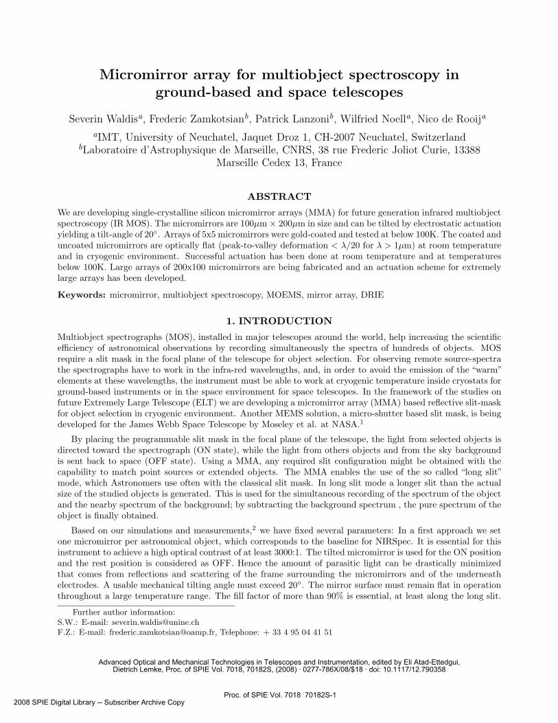
Figure 2. Surface quality of the micromirrors. Topographic images obtained from a phase shift interferometric setup (a) ofa 100µm x 200µm micromirror in the OFF position (b) in the ON position and (c) of a large 250µm x 500µm micromirrorin the ON state. The surface quality is not degraded when the mirror is actuated. The peak-to-valley deformation of thesmaller mirrors is 8nm and 15nm in the case of the larger mirrors. The RMS roughness is around 1nm in both cases.
One micromirror element has to be around 100µm × 200µm - the exact value depends on the plate scale andoptical design of the concerned telescope. The micromirror array has to work at cryogenic temperatures.
We developed and fabricated 5 × 5 micromirror arrays which fulfill above key requirements. Large arraysof 200 × 100 micromirrors, which is considered as an usable arrays size for the use in a real system, are underdevelopment. The results of the fabricated micromirror devices is summarized in Fig. 1 and presented earlier.3
The micromirrors are actuated electrostatically by an electrode located on a second chip, which is fabricatedseparately and assembled subsequently (Fig. 1). The micromirrors are made of single-crystalline silicon, assuringoptical flat surfaces. Silicon being transparent in the infrared range, a gold thin-film coating is deposited onthe topside of the mirrors. The cantilever-type suspension is made of a deposited poly-crystalline silicon layerdeposited on the back of the mirror. This hidden (or stacked) suspension enables high fill-factor and reducesstray light originating from the cantilevers that are bent in operation. A system of multiple stopper beamslocated on the mirror and on the frame provides precise and uniform tilt-angle. The tilt-angle is uniform withinone arcminute over a range of 15V of actuation voltage and over the whole array.
In this paper we focus on the optical quality of the mirrors, the effect of the optical coating and cryogenicenvironment required for infrared operation. Furthermore we present an approach how we intend to deal withthe very large number of micromirrors required for the application in a real system, where object selection overa large field is required. A demonstration of objection selection over a small field using the 5x5 demonstratordevice is given afterwards.
2. OPTICAL CHARACTERIZATION
A dedicated characterization bench has been developed for the complete analysis of MOEMS devices, actua-tors or micro-mirrors as well as full arrays. This modular Twyman-Green interferometer allows high in-planeresolution (3µm) or large field of view (40mm). Out-of-plane measurements are performed with phase-shiftinginterferometry showing very high resolution (standard deviation < 1nm). Features such as optical quality orelectro-mechanical behavior are extracted from these high precision three-dimensional component maps. Rangeis increased without loosing accuracy by using two-wavelength phase-shifting interferometry authorizing largesteps measurements.4 All measurements have been confirmed with a Veeco/Wyko NT1100 DMEMS opticalprofiler.
The surface quality of uncoated mirrors was measured in the OFF and the ON state: Fig. 2. The 100µm × 200µmsized mirrors showed a peak-to-valley deformation of 7nm, in OFF position as well in ON position - the mirrorsremain flat when operated. Larger mirrors of 250µm × 500µm, which may be used for larger telescopes, showeda PTV of 15nm, still satisfying the requirement on optical flatness. The local roughness is comparable to apolished silicon wafer, which is around 1nm RMS - using the backside of the device layer as mirror topside yieldsthis almost flawless surface, as the device layer backside remains protected by the buried oxide layer throughoutthe whole fabrication process and is exposed only in the very last step.
Proc. of SPIE Vol. 7018 70182S-3
Xi 97.9975 urn
a) no coating P1Vc 1 Onm 2m 'V
_______________________o ig 20 30 40 50 00 70 80 00 100 lID 120 130 140 150 ISO 170 IOU 803 200
b) single-side coating PlVc35nm
tin
Ii
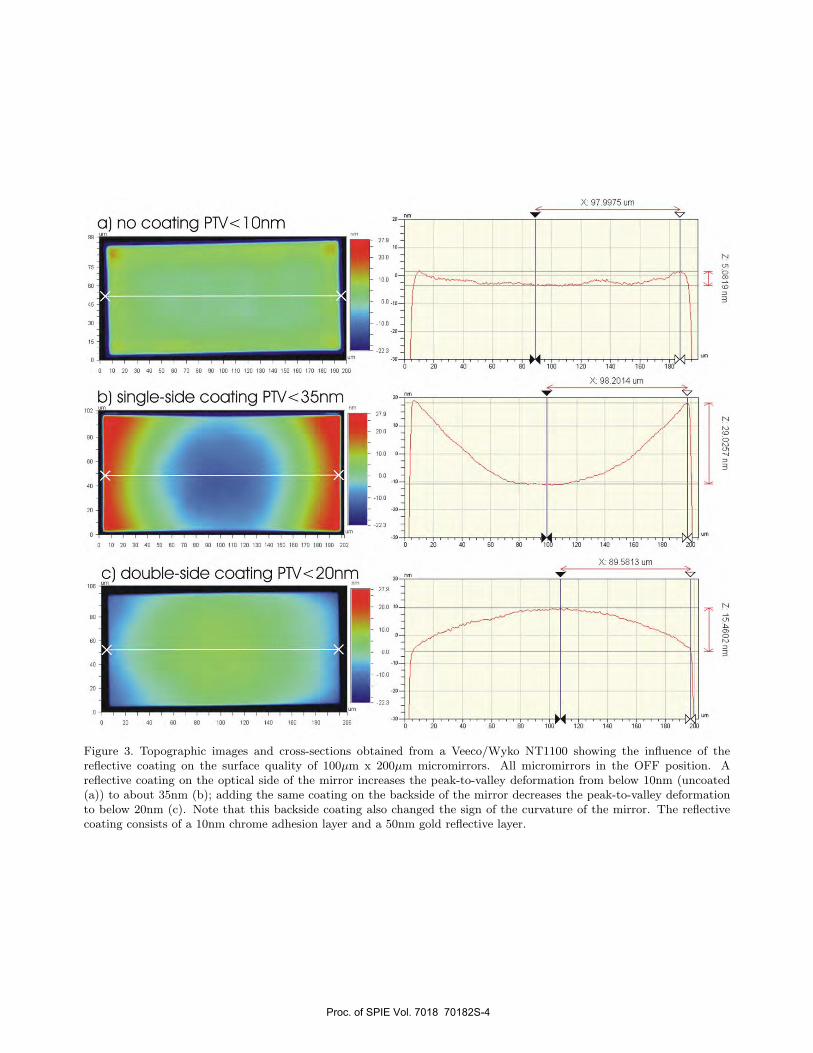
Figure 3. Topographic images and cross-sections obtained from a Veeco/Wyko NT1100 showing the influence of thereflective coating on the surface quality of 100µm x 200µm micromirrors. All micromirrors in the OFF position. Areflective coating on the optical side of the mirror increases the peak-to-valley deformation from below 10nm (uncoated(a)) to about 35nm (b); adding the same coating on the backside of the mirror decreases the peak-to-valley deformationto below 20nm (c). Note that this backside coating also changed the sign of the curvature of the mirror. The reflectivecoating consists of a 10nm chrome adhesion layer and a 50nm gold reflective layer.
Proc. of SPIE Vol. 7018 70182S-4

b)
92K, UVFigure 4. Cryogenic setup and functional characterization. (a) Cryogenic chamber installed on an interferometric setup.On the picture the chamber cover is removed, showing the packaged micromirror array mounted on a dedicated printedcircuit board in the chamber. (b-c) Functional testing of the micromirror array. One line of micromirrors, initially in theoff-state (b) is switched into the ON state (c).
Figure 5. Interferometric measurement of the mirror quality on the cryogenic testbench. At room temperature the gold-coated micromirror show a peak-to-valley deformation of 36nm (a) and at below 100K a peak-to-valley deformation of50nm (b).
Using a reflective layer increases the mirror deformation. A 50nm gold layer, with a 10nm chrome adhesionlayer, is deposited on the micromirrors for good reflectivity in the near and mid-infrared range. The peak-to-valley deformation increases to about 35nm when coating only the topside of the mirror. Additionally coatingthe backside of the mirror with the identical layers decreases the peak-to-valley deformation to 17nm (Fig. 3).Note that the curvature of the mirror changed from concave to convex. In theory, a perfectly balanced sandwichcoating would yield the initial deformation of the uncoated mirror; however in our case the backside of the mirroris partially shadowed by the suspension beams leading to a geometric asymmetry between the front- and backsidecoating and thus inducing this residual deformation.
3. CRYOGENIC CHARACTERIZATION
3.1 Experimental setup
The cryogenic compatibility is crucial for the application in an infrared (IR) MOS. The operating temperaturemust be below 100K for near and mid IR and below 40K for far IR. Our MMA is conceived such that all structural
Proc. of SPIE Vol. 7018 70182S-5
elements have a matched coefficient of thermal expansion (CTE) in order to avoid deformation or even flakingwithin the device when cooling down to the operating temperature. The mirrors themselves must be coveredwith a gold layer for IR operation, gold having a different CTE than silicon. As the silicon mirror is 10µm thickand the coating 60nm thin, we estimate that the induced deformation will be small.
Cryogenic characterization was carried out in a custom built cryogenic chamber installed on our interfer-ometric setup (Fig. 4). The cryo-chamber has a pressure as low as 10e-6 mbar and is able to cool down to60K, using a cryogenic generator. In order to get such temperature, the chamber is equipped with an internalscreen insulating radiatively the sample from the chamber. Control of the environment is obtained by means oftemperature sensors and local heaters. They are wired to the outside environment through a Dutch connectorand connected to a custom built control electronics.
The chamber has a glass window that allows observing and measuring the sample chip during cryogenictesting. The micro-mirror device is illuminated and imagined by a CCD camera on the outside; the micro-mirrordevice is rotated such that the light of the tilted mirrors (ON state) is sent to the CCD camera. The presence ofa glass window at the entrance of the chamber is an issue for getting fringes with a high contrast. Two elementshave to be corrected:
• The path difference between the interferometer arms (sample arm and reference mirror arm)
• The glass medium is dispersive for the different wavelengths, each wavelength following a different path.
The first point could be overcome by moving the reference mirror in order to balance the path differenceinduced by the index difference between the window material and air, this balance is obtained for a very narrowlinewidth. As we are using sources with low coherence, i. e. with a wide linewidth (typically 10nm), and asglass is dispersive, the path followed by each wavelength will be slightly different, degrading drastically the fringepattern contrast. The only solution is to introduce in the reference arm a glass plate exactly identical to thewindow in the sample arm. Usually this plate has to be ordered at the same time the window is ordered, forgetting perfectly identical components. Unfortunately, we didn’t have such plate, and we had to introduce anavailable glass plate with a thickness slightly different from the actual window. This may cause a degradationof the fringe pattern contrast, increasing the measurement noise, but this does not degrade the measurementaccuracy.
The PGA84 housing containing the sample chip is mounted via a spring loaded grid zip connector on aspecially conceived printed circuit board (PCB). Large copper surfaces on the PCB facilitate cooling down thesystem; renouncing the solder-stop layer eases outgassing of the PCB FR4 base material during evacuation of thechamber. The PCB itself is mounted via a fix-point-plane-plane attachment system to a solid aluminum block,the latter being interconnected to the cryo-generator. Thick copper wires between the PCB and the aluminumblock further enhance thermal transport between the sample chip and the cryostat. Teflon-isolated electrical wiresallow to interconnect up to 27 electrical connections through a Dutch connector to the outside environment. Onthe outside environment the wires are connected to a custom built control electronics. Temperature sensors areconnected to the aluminum block and to the grid zip connector adjacent to the sample chip.
3.2 Cryogenic measurements
The cryogenic chamber was cooled down until thermal equilibrium was reached. This yielded a temperatureof 64K measured at the aluminum block and 86K measured adjacent to the sample chip. From experience theactual temperature on the chip was estimated to be about 10K higher than on the temperature sensor adjacent.The pressure in the chamber was at 10−6mbar. The chip could successfully be actuated before, during and aftercryogenic testing. Single mirrors were actuated, as well lines of micromirrors, implementing the so-called longslit mode. Fig. 4 (b-c) shows the transition from OFF to the ON state of a line of micromirros in cryogenicenvironment. This proves that the micromirror device remains functional below 100K. The actuation voltage forthe mirror to snap from the OFF to the ON position was identical before and after cryogenic testing, indicatingthat there is no mechanical degradation of the different material interfaces. This result was confirmed by staticobservation in a Philips ESEM at 120K; no degradation of the critical parts of the device could be seen, the
Proc. of SPIE Vol. 7018 70182S-6
latter being: interface between electrode and mirror chip, polysilicon - single-crystalline-silicon interface and goldcoating - silicon interface.
Figure 5 shows the surface quality measured of one gold-coated micromirror in the cryogenic setup. Thesurface quality was measured after mounting the micromirror device on the PCB in the cryogenic chamber, atroom temperature and before closing the chamber (Fig. 5 (a)). The peak-to-valley deformation here was 36nm,which corresponds to the measurements made before outside the cryogenic chamber (see previous section). Fig. 5(b) shows the measurement made after closing the chamber and cooling down below 100K. The deformationshape of the mirror remains identical compared to room temperature. As expected, due the CTE mismatchbetween the silicon substrate and the gold-coating, the peak-to-valley deformation increases to 50nm. The lowersignal-to-noise ratio in this measurement has been induced by the presence of the window at the entrance ofthe cryogenic chamber. Note that the lower signal-to-noise ratio does not degrade the measurement accuracy ofthe mirror curvature. The measured value of the peak-to-valley deformation at 100K is in good agreement withthe estimated value in Section 2, where a value of 52nm was found. This deformation of 50nm is within therequirement of λ/20 at λ = 1µm. For lower temperatures however a thicker substrate or a titanium (instead ofchromium) adhesion layer for the gold coating has to be used.5
4. LARGE ARRAY ACTUATION
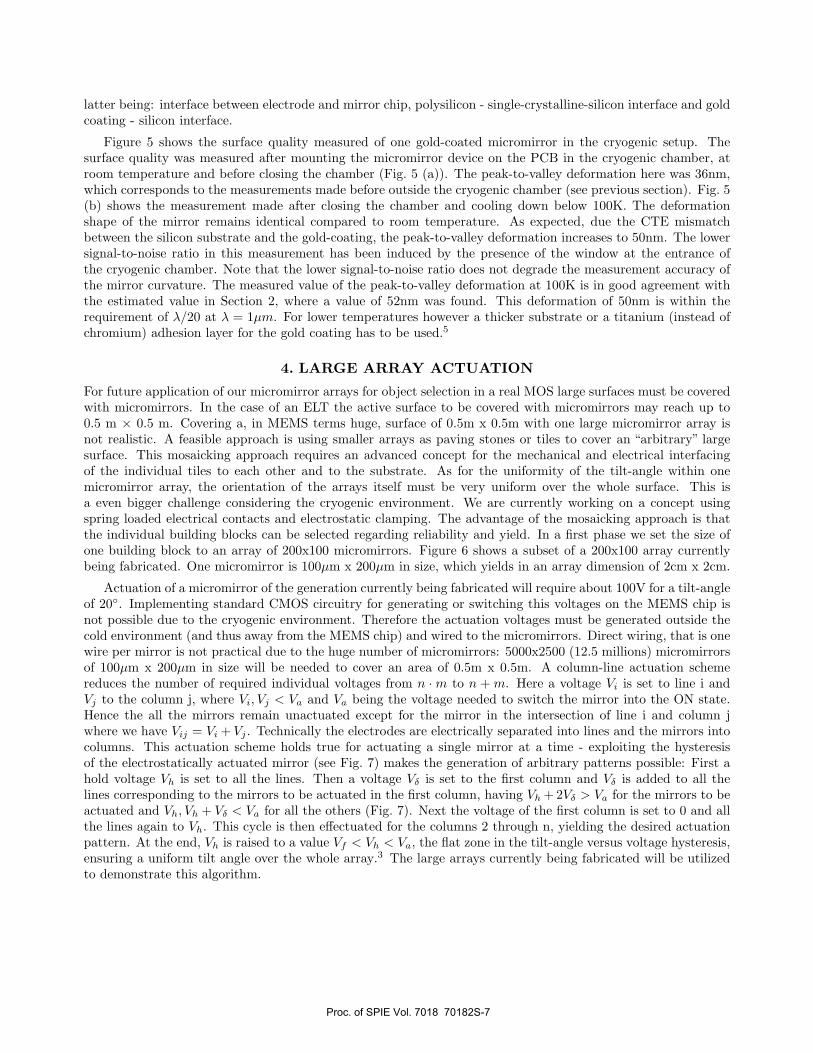
For future application of our micromirror arrays for object selection in a real MOS large surfaces must be coveredwith micromirrors. In the case of an ELT the active surface to be covered with micromirrors may reach up to0.5 m × 0.5 m. Covering a, in MEMS terms huge, surface of 0.5m x 0.5m with one large micromirror array isnot realistic. A feasible approach is using smaller arrays as paving stones or tiles to cover an “arbitrary” largesurface. This mosaicking approach requires an advanced concept for the mechanical and electrical interfacingof the individual tiles to each other and to the substrate. As for the uniformity of the tilt-angle within onemicromirror array, the orientation of the arrays itself must be very uniform over the whole surface. This isa even bigger challenge considering the cryogenic environment. We are currently working on a concept usingspring loaded electrical contacts and electrostatic clamping. The advantage of the mosaicking approach is thatthe individual building blocks can be selected regarding reliability and yield. In a first phase we set the size ofone building block to an array of 200x100 micromirrors. Figure 6 shows a subset of a 200x100 array currentlybeing fabricated. One micromirror is 100µm x 200µm in size, which yields in an array dimension of 2cm x 2cm.
Actuation of a micromirror of the generation currently being fabricated will require about 100V for a tilt-angleof 20◦. Implementing standard CMOS circuitry for generating or switching this voltages on the MEMS chip isnot possible due to the cryogenic environment. Therefore the actuation voltages must be generated outside thecold environment (and thus away from the MEMS chip) and wired to the micromirrors. Direct wiring, that is onewire per mirror is not practical due to the huge number of micromirrors: 5000x2500 (12.5 millions) micromirrorsof 100µm x 200µm in size will be needed to cover an area of 0.5m x 0.5m. A column-line actuation schemereduces the number of required individual voltages from n · m to n + m. Here a voltage Vi is set to line i andVj to the column j, where Vi, Vj < Va and Va being the voltage needed to switch the mirror into the ON state.Hence the all the mirrors remain unactuated except for the mirror in the intersection of line i and column jwhere we have Vij = Vi + Vj . Technically the electrodes are electrically separated into lines and the mirrors intocolumns. This actuation scheme holds true for actuating a single mirror at a time - exploiting the hysteresisof the electrostatically actuated mirror (see Fig. 7) makes the generation of arbitrary patterns possible: First ahold voltage Vh is set to all the lines. Then a voltage Vδ is set to the first column and Vδ is added to all thelines corresponding to the mirrors to be actuated in the first column, having Vh + 2Vδ > Va for the mirrors to beactuated and Vh, Vh + Vδ < Va for all the others (Fig. 7). Next the voltage of the first column is set to 0 and allthe lines again to Vh. This cycle is then effectuated for the columns 2 through n, yielding the desired actuationpattern. At the end, Vh is raised to a value Vf < Vh < Va, the flat zone in the tilt-angle versus voltage hysteresis,ensuring a uniform tilt angle over the whole array.3 The large arrays currently being fabricated will be utilizedto demonstrate this algorithm.
Proc. of SPIE Vol. 7018 70182S-7
0 20 40 60 #0 100 120
Voltage LV]
45
6
m
ye 0 0 0 01 2 34 5 ...n
2VS 2Vo
+ _ve
+ _ve
2
3
— — — —
1Vh +
Figure 6. (a) Optical microscope image of a 200x100 large micromirror array (MMA) currently being fabricated. Onemicromirror element is 100µm x 200µm in size, the complete array 2cm x 2cm. (b) Mosaicking of these MMA can be usedto cover arbitrary large surfaces.
Figure 7. Electrostatic hysteresis of one micromirror. The column-line addressing scheme is used to generate randompatterns on large arrays – requiring only n+m voltages exploiting the electrostatic hysteresis of the micromirrors.
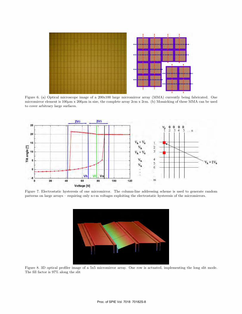
Figure 8. 3D optical profiler image of a 5x5 micromirror array. One row is actuated, implementing the long slit mode.The fill factor is 97% along the slit
Proc. of SPIE Vol. 7018 70182S-8
I PoIychromIicSources Mooochramatic
I Various sizesFine positioning
CCD IMMAimaging
inputpupil
£T
Outputpupil
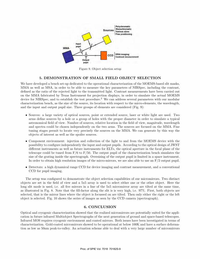
Figure 9. Object selection setup
5. DEMONSTRATION OF SMALL FIELD OBJECT SELECTION
We have developed a bench set-up dedicated to the operational characterization of the MOEMS-based slit masks,MMA as well as MSA, in order to be able to measure the key parameters of NIRSpec, including the contrast,defined as the ratio of the rejected light to the transmitted light. Contrast measurements have been carried outon the MMA fabricated by Texas Instrument for projection displays, in order to simulate the actual MOEMSdevice for NIRSpec, and to establish the test procedure.2 We can address several parameters with our modularcharacterization bench, as the size of the source, its location with respect to the micro-elements, the wavelength,and the input and output pupil size. Three groups of elements are considered (Fig. 9):
• Sources: a large variety of optical sources, point or extended source, laser or white light are used. Twoarms define sources by a hole or a group of holes with the proper diameter in order to simulate a typicalastronomical field of view. Number of sources, relative location in the field of view, magnitude, wavelengthand spectra could be chosen independently on the two arms. The sources are focused on the MMA. Finetuning stages permit to locate very precisely the sources on the MMA. We can generate by this way theobjects of interest as well as the spoiler sources.
• Component environment: injection and collection of the light to and from the MOEMS device with thepossibility to configure independently the input and output pupils. According to the optical design of JWSTdifferent instruments as well as future instruments for ELTs, the optical aperture in the focal plane of thetelescope could be tuned from F/6 to F/50. The output pupil of the characterization bench simulates thesize of the grating inside the spectrograph. Oversizing of the output pupil is limited in a space instrument.In order to obtain high resolution images of the micro-mirrors, we are also able to use an F/2 output pupil.
• Detectors: a high dynamical range CCD for device imaging and contrast measurement, and a conventionalCCD for pupil imaging.
The setup was configured to demonstrate the object selection capabilities of our micromirrors. Two distinctobjects are set in the field of view and a 5x5 array is used to select either one or the other object. Here thelong slit mode is used, i.e. all five mirrors in a line of the 5x5 micromirror array are tilted at the same time,as illustrated in Fig. 8. Note that the fill-factor along the slit is is very high, i.e. 97%. First, both objects areselected, that is the mirror lines where the object is focussed on are tilted. Then only either the right or the leftobject is selected. Fig. 10 shows the series of images as seen by the CCD camera (spectrograph).
6. CONCLUSION
Optical and cryogenic characterization showed that the realized micromirrors are potentially suited for the appli-cation in future infrared Multiobject Spectrographs of the next generation of ground and space-based telescopes.Infrared MOS requires cryogenic environment and coated mirrors. Both issues have been investigated in terms ofcharacterization. Gold-coated micromirrors showed to be operational at below 100K and have a surface deforma-tion as low as 50nm peak-to-valley. An actuation scheme able to deal with a very large number of micromirrors
Proc. of SPIE Vol. 7018 70182S-9
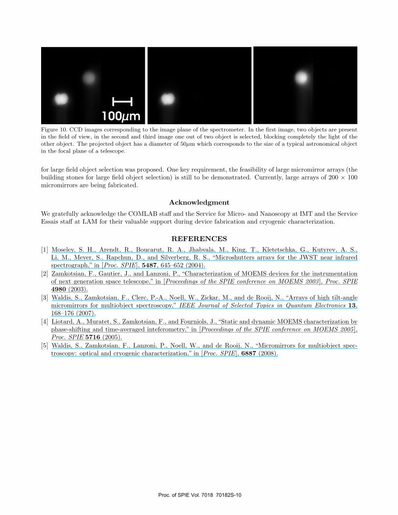
Figure 10. CCD images corresponding to the image plane of the spectrometer. In the first image, two objects are presentin the field of view, in the second and third image one out of two object is selected, blocking completely the light of theother object. The projected object has a diameter of 50µm which corresponds to the size of a typical astronomical objectin the focal plane of a telescope.
for large field object selection was proposed. One key requirement, the feasibility of large micromirror arrays (thebuilding stones for large field object selection) is still to be demonstrated. Currently, large arrays of 200 × 100micromirrors are being fabricated.
Acknowledgment
We gratefully acknowledge the COMLAB staff and the Service for Micro- and Nanoscopy at IMT and the ServiceEssais staff at LAM for their valuable support during device fabrication and cryogenic characterization.
REFERENCES[1] Moseley, S. H., Arendt, R., Boucarut, R. A., Jhabvala, M., King, T., Kletetschka, G., Kutyrev, A. S.,
Li, M., Meyer, S., Rapchun, D., and Silverberg, R. S., “Microshutters arrays for the JWST near infraredspectrograph,” in [Proc. SPIE ], 5487, 645–652 (2004).
[2] Zamkotsian, F., Gautier, J., and Lanzoni, P., “Characterization of MOEMS devices for the instrumentationof next generation space telescope,” in [Proceedings of the SPIE conference on MOEMS 2003 ], Proc. SPIE4980 (2003).
[3] Waldis, S., Zamkotsian, F., Clerc, P.-A., Noell, W., Zickar, M., and de Rooij, N., “Arrays of high tilt-anglemicromirrors for multiobject spectroscopy,” IEEE Journal of Selected Topics in Quantum Electronics 13,168–176 (2007).
[4] Liotard, A., Muratet, S., Zamkotsian, F., and Fourniols, J., “Static and dynamic MOEMS characterization byphase-shifting and time-averaged inteferometry,” in [Proceedings of the SPIE conference on MOEMS 2005 ],Proc. SPIE 5716 (2005).
[5] Waldis, S., Zamkotsian, F., Lanzoni, P., Noell, W., and de Rooij, N., “Micromirrors for multiobject spec-troscopy: optical and cryogenic characterization,” in [Proc. SPIE ], 6887 (2008).
Proc. of SPIE Vol. 7018 70182S-10
Related Documents

![Datareductionoflargevectorgraphics - cs.uef.fics.uef.fi/sipu/pub/MultiObject-PR2005.pdf · Fast algorithm for joint near-optimal approximation of multiple polygonal ... [17–19,26]](https://static.cupdf.com/doc/110x72/5b8765917f8b9a1f248c9b00/datareductionoflargevectorgraphics-csuefficsueffisipupubmultiobject-.jpg)