3D holographic Polymer Photonic Crystal for Superprism Application Jiaqi Chen a) , Wei Jiang b) , Xiaonan Chen a) , Li Wang a) , Sasa Zhang a) and Ray T.Chen* a) Microelectronics Research Center, Department of Electrical and Computer Engineering, The University of Texas at Austin, Austin, TX 78758 b) Omega Optics, Inc. Austin, TX 78758 * Electronic mail: [email protected] ABSTRACT Photonic crystal based superprism offers a new way to design new optical components for beam steering and DWDM application. 3D photonic crystals are especially attractive as they could offer more control of the light beam based on the needs. A polygonal prism based holographic fabrication method has been demonstrated for a three-dimensional face- centered-cubic (FCC)-type submicron polymer photonic crystal using SU8 as the photo-sensitive material. Therefore antivibration equipment and complicated optical alignment system are not needed and the requirement for the coherence of the laser source is relaxed compared with the traditional holographic setup. By changing the top-cut prism structure, the polarization of the laser beam, the exposure and development conditions we can achieve different kinds of triclinic or orthorhombic photonic crystals on demand. Special fabrication treatments have been introduced to ensure the survivability of the fabricated large area (cm 2 ) nano-structures. Scanning electron microscopy and diffraction results proved the good uniformity of the fabricated structures. With the proper design of the refraction prism we have achieved a partial bandgap for S+C band (1460-1565nm) in the [111] direction. The transmission and reflection spectra obtained by Fourier transform infrared spectroscopy (FTIR) are in good agreement with simulated band structure. The superprism effects around 1550nm wavelength for the fabricated 3D polymer photonic crystal have been theoretically calculated and such effects can be used for beam steering purpose. Keywords: polymer, three-dimensional photonic crystal, holography, SU8, superprism. 1. Introduction The prediction and the confirmation that artificial periodic dielectric structures can be used to manipulate electromagnetic wave propagation affect significantly the development of the micro- and nano-optoelectronics. 1-4 One of the many interesting phenomena is superprsim effect in the photonic crystal. It is the anomalous refraction of light at an interface between a photonic crystal and a homogeneous medium. The refraction angle is found to be very sensitive to the change of incident angle and wavelength under proper conditions. Such effect arises from the anisotropy of the bands in the photonic crystal and such dispersion effects could be hundreds times stronger than the conventional prism. And that is where it gains the name “superprism”. A number of groups have previously designed and fabricated superprsim devices since its introduction by Kosaka and co-workers 5 . Superprism effect in two-dimensional periodic systems was investigated by Baba et al. 6 and Chung et al. 7 afterward. The first experimental demonstration of 2D superprism effect was reported by Wu et al. 8 who employed an asymmetric GaAs-AlGaAs heterostructure to provide light confinement in the third dimension via total internal reflection. On the other hand, in the 3D photonic crystal case by careful design you can get a better control of light in all the directions, and you can achieve a more versatile design. Also the 3D photonic crystal can offer you a real 3D superprism effect instead of the in-plane superprism effect. In the literature there is a great diversity in the fabrication approaches to make two-dimensional and three-dimensional photonic crystals. Therefore, it

Welcome message from author
This document is posted to help you gain knowledge. Please leave a comment to let me know what you think about it! Share it to your friends and learn new things together.
Transcript
3D holographic Polymer Photonic Crystal
for Superprism Application
Jiaqi Chena), Wei Jiang b), Xiaonan Chen a), Li Wang a), Sasa Zhang a) and Ray T.Chen*
a) Microelectronics Research Center, Department of Electrical and Computer Engineering,
The University of Texas at Austin, Austin, TX 78758
b) Omega Optics, Inc. Austin, TX 78758
* Electronic mail: [email protected]
ABSTRACT
Photonic crystal based superprism offers a new way to design new optical components for beam steering and DWDM application. 3D photonic crystals are especially attractive as they could offer more control of the light beam based on the needs. A polygonal prism based holographic fabrication method has been demonstrated for a three-dimensional face-centered-cubic (FCC)-type submicron polymer photonic crystal using SU8 as the photo-sensitive material. Therefore antivibration equipment and complicated optical alignment system are not needed and the requirement for the coherence of the laser source is relaxed compared with the traditional holographic setup. By changing the top-cut prism structure, the polarization of the laser beam, the exposure and development conditions we can achieve different kinds of triclinic or orthorhombic photonic crystals on demand. Special fabrication treatments have been introduced to ensure the survivability of the fabricated large area (cm2) nano-structures. Scanning electron microscopy and diffraction results proved the good uniformity of the fabricated structures. With the proper design of the refraction prism we have achieved a partial bandgap for S+C band (1460-1565nm) in the [111] direction. The transmission and reflection spectra obtained by Fourier transform infrared spectroscopy (FTIR) are in good agreement with simulated band structure. The superprism effects around 1550nm wavelength for the fabricated 3D polymer photonic crystal have been theoretically calculated and such effects can be used for beam steering purpose. Keywords: polymer, three-dimensional photonic crystal, holography, SU8, superprism. 1. Introduction The prediction and the confirmation that artificial periodic dielectric structures can be used to manipulate electromagnetic wave propagation affect significantly the development of the micro- and nano-optoelectronics.1-4 One of the many interesting phenomena is superprsim effect in the photonic crystal. It is the anomalous refraction of light at an interface between a photonic crystal and a homogeneous medium. The refraction angle is found to be very sensitive to the change of incident angle and wavelength under proper conditions. Such effect arises from the anisotropy of the bands in the photonic crystal and such dispersion effects could be hundreds times stronger than the conventional prism. And that is where it gains the name “superprism”. A number of groups have previously designed and fabricated superprsim devices since its introduction by Kosaka and co-workers5. Superprism effect in two-dimensional periodic systems was investigated by Baba et al.6 and Chung et al.7 afterward. The first experimental demonstration of 2D superprism effect was reported by Wu et al.8 who employed an asymmetric GaAs-AlGaAs heterostructure to provide light confinement in the third dimension via total internal reflection. On the other hand, in the 3D photonic crystal case by careful design you can get a better control of light in all the directions, and you can achieve a more versatile design. Also the 3D photonic crystal can offer you a real 3D superprism effect instead of the in-plane superprism effect. In the literature there is a great diversity in the fabrication approaches to make two-dimensional and three-dimensional photonic crystals. Therefore, it
is needed to improve the quality in terms of being more feature-size flexible, materials flexible and less time consuming. Despite the remarkable progress in the fabrication of two-dimensional photonic crystals,9 there remain significant challenges for the fabrication of 3D photonic crystals, especially for producing sub-micron periodicity for near-IR applications. Many 3D fabrication approaches have been studied on a number of material platforms. Among them, layer-by-layer stacking using soft lithography or nanoimprint,10 microassembly of planar semiconductor layers11 and multi-photon absorption12 have been investigated to create certain microstructures. However, for the aforementioned approaches multiple processing steps are generally required and they are not suitable for larger scale (cm2 size) fabrication. Recently, after Campbell and coworkers13 successfully demonstrated the holographic fabrication of 3D photonic crystal, holographic lithography has gained more and more attentions in the fabrication of 3D polymer photonic crystals. By controlling the propagation directions, phases and polarizations of the multiple laser beams one can generate a desired 3D laser interference pattern to expose a photo-sensitive materials such as photoresist and render the exposed area soluble or insoluble depends on the material type in use. This process allows flexible design and a control of the unit cell geometry, therefore of the desired optical properties. And it has been proven theoretically that all fourteen Bravais lattices can be constructed using such a method. 14 In the early days of this approach multiple beams were formed by independent optical components. Such setups were complicated and required careful alignment. Recently, Divliansky et al.15 introduced a diffraction mask to create the four desired beams and Wu et al.16 demonstrated another idea using a single refracting prism to split and combine the desired beams. With the use of a single optical element to split and recombine the laser beams, sophisticated anti-vibration system and alignment are avoided. However, the photonic bandgap and superprism effect of most of these devices did not fall in the optical communication windows due to the relatively large period. Here based on the diffraction prism approach we used a He-Cd 325 nm wavelength laser to fabricate submicron 3D photonic crystal structure using a negative i-line resist SU8 for the superprism application near 1550 nm. 2. Fabrication process The optical setup for the fabrication using SU8 is illustrated in Fig. 1(a).
(a) (b)
(c) Figure 1(a). A schematic of the holographic lithography setup. The collimated laser beam is reflected by a mirror towards the prism and the glass substrate. (b) The coupling top-cut prism has a symmetric structure. The top and bottom surfaces are equilateral triangles with edges of L1 and L2 respectively. The cutting angle determines the final refracted beam position and can be calculated by

)](2/[3)tan( 12 LLH −×=φ . (c) A schematic of the positions of the prism, glass substrate and the absorption plate for the use of negative photoresist. The UV (325nm) laser beam coming from the He-Cd laser was expanded using a UV objective lens. The spatial filter afterward cleaned up the unwanted scattering in the optical path to ensure a good beam quality. After the laser beam was collimated by a large lens it hit normally on the special designed top-cut prism. The prism was made from the JGS1 material (n=1.482 @320nm) to achieve a larger than 95% UV transmission and the surfaces of the polygonal prism had been polished to make the transmission intensity as large as possible. The three sidewalls of the top-cut prism created three side beams by beam refraction. The center beam of this umbrella interference configuration was formed from the central part of the collimated laser beam going through the top and bottom surfaces of the prism. The individual incident
plane wave is iii etrGiE rrv*)exp(* ω−• and all the incident waves have the same frequency but with different
polarization and intensity due to the refraction at the prism interface. The four beams created by the prism overlapped at the bottom of the prism. By controlling the height of the prism one could control the depth of overlap to ensure the photoresist are within the overlap volume. In our design shown in Fig. 1(b) L1=1cm, L2=4cm and H=1.5cm therefore we achieved a cutting angle of 60 ° for the prism. Then the resulting wave vectors were
)1,0,0(20 −=
λπG , )239.1914,-0.9-0.3314,-0(2
1 λπ
=G , )391914,-0.920.3314,-0.(22 λ
π=G ,
)0.92390,0.3827,-(23 λ
π=G , where λ = 325nm in our case. With the polarization of the incident laser beam aligned
with the x-axis in the system, the resulting polarization for the four beams are )0 , ,0 1(0 =e , )7055,-0.3380.9409,0.0(1 =e , )70055,0.3380.9409,-0.(2 =e , )0,0,1(3 =e
The interference pattern can be calculated by
Where 4=N , jiijii KKKGGK −=−= ,0 and sθ are the phase differences of the beams.
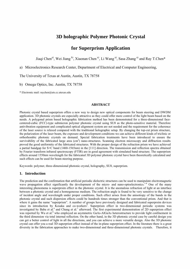
As shown in Fig. 1(c) the bottom black glass plate was used to reduce the back-reflected light and all the interfaces used index matching liquid to avoid the unwanted reflections at the glass/air and polymer/air interfaces. To model the fabrication of the 3D holographic lithography process more accurately we need to consider the absorption of the laser beam inside the photoresist.17 Since such optical absorption during the exposure process caused the geometry of the fabricated photonic crystal to change with the depth. Although it would not affect the period, the filling factor and the shape of the final structure would vary with depth. For the top-side exposure employed here, lower portion of the photoresist received less energy than near the surface. With reduced size, the reliability of the actual fabricated structures would be more influenced by such absorption. Fig. 2s show the computer simulations of FCC type photonic crystal obtained from four-beam interference with and without absorption using the K vectors obtained before and an SU8 absorption 0.1/μm @ 330 nm.
∑ ∑∑−
=
−
=>
−
=
∗
+•×•××++•×•××+=
•=1
1
1
100
1
0
2 )cos(2)cos(2
),(),()(N
i
N
jiijijjijiiiii
N
ii
totaltotal
rKeeEErKeeEEE
trEtrErI
θθ rrrrrrrr
rrr
(a) (b)
Figure 2 (a) Simulation of intensity distribution in the photoresist without considering the absorption. (b) Simulation of intensity distribution in the photoresist considering the absorption.
The blue volume enclosed by the green surface has an exposure dosage above the polymerization threshold and would be insoluble during development for a negative resist. It is not trivial for a negative resist 3D photonic crystal with a small feature size structure to survive the development owing to the potentially violent capillary force on a microscopic scale. Particularly, it is critical to ensure good substrate adhesion and avoid the structural damage originating from the capillary drainage of the rinsing liquid during the drying process.18 From the simulation results accounting for the absorption, it is obvious that since the bottom part of the resist receives less effective dosage the top portions became more fully cross linked and remained bulkier in the final structure. As less SU8 resist would remain at the bottom part after development, it is highly susceptible to damage during the drying process. The standard SU-8 rinsing liquid is isopropanol, and it has a surface tension γ of 23 mN/m and a contact angle θ =20 °. On the contrary, when considering the wetting characteristic although DI Water has a higher surface tension of 73mN/m, it has a contact angle of 81° due to the hydrophobic nature of the SU8 material. As the capillary force is proportional to )cos(θγ , the capillary force exerted by water is about twice smaller than that by isopropanol and we switched to use DI water as the rinse liquid for all fabricated samples. No peel-off was observed in the experiments. In the experiments we used photoresist coated on a glass substrate for the recording of the 3D structures. The negative resist we used was a commercially available SU-8 2007 from Microchem Inc. After the spin coating, the substrate was baked at 95°C to evaporate the solvent and we achieved a thickness of about 10μm. The 325nm line from the He-Cd CW laser was used to expose the sample and the light intensity was about 5.37mW/ cm2. The index matching liquid employed was silicone oil which has no reaction with SU8. After the exposure we applied a post-exposure bake at 95 °C. The unexposed film was removed by PGMEA and rinsed in DI water.
3. Fabrication results and verification of the formation of good 3D photonic crystal structure Fig. 3 shows the SEM images and diffraction pattern of the fabricated 3D polymer photonic crystal structures. The total area is decided by the size of the prism and in our case it is an equilateral triangle with an edge of 1cm. Fig. 3(a) exhibits the whole size and a fracture of the 3D FCC-type structure using SU8. The detailed fine structures in the (111) plane is presented in Fig. 3(b) with good uniformity. The enlarged side view of the cleaved SU8 sample with 6 layers is shown in Fig. 3(c). For the structures fabricated in the SU8 resist under the SEM observation, (111) in-plane and perpendicular lattice spacing were measured to be 0.61 and 2.02μm respectively. The simulation results showed (111) in-plane and perpendicular lattice spacing to be 0.63 and 2.10μm which are slightly larger than the fabrication results. Such differences can be attributed to the size error of the prism and the shrinkage of the photoresist after the bake process.
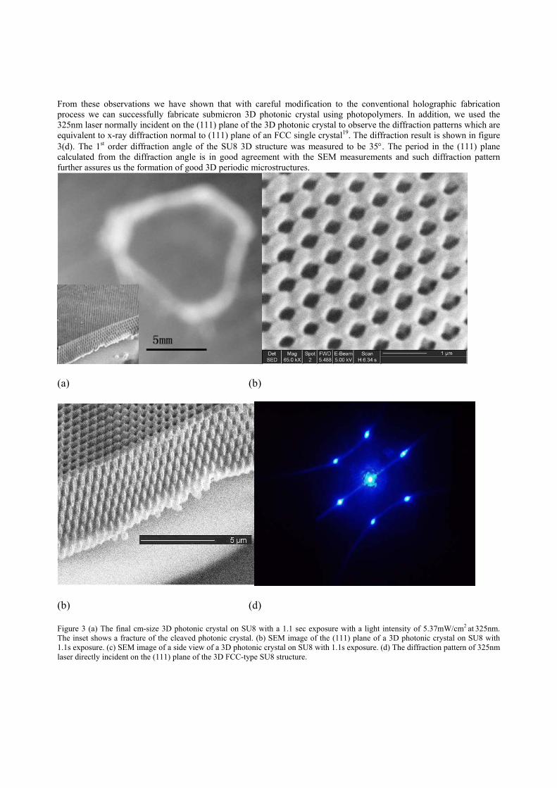
From these observations we have shown that with careful modification to the conventional holographic fabrication process we can successfully fabricate submicron 3D photonic crystal using photopolymers. In addition, we used the 325nm laser normally incident on the (111) plane of the 3D photonic crystal to observe the diffraction patterns which are equivalent to x-ray diffraction normal to (111) plane of an FCC single crystal19. The diffraction result is shown in figure 3(d). The 1st order diffraction angle of the SU8 3D structure was measured to be 35°. The period in the (111) plane calculated from the diffraction angle is in good agreement with the SEM measurements and such diffraction pattern further assures us the formation of good 3D periodic microstructures.
(a) (b)
(b) (d)
Figure 3 (a) The final cm-size 3D photonic crystal on SU8 with a 1.1 sec exposure with a light intensity of 5.37mW/cm2 at 325nm. The inset shows a fracture of the cleaved photonic crystal. (b) SEM image of the (111) plane of a 3D photonic crystal on SU8 with 1.1s exposure. (c) SEM image of a side view of a 3D photonic crystal on SU8 with 1.1s exposure. (d) The diffraction pattern of 325nm laser directly incident on the (111) plane of the 3D FCC-type SU8 structure.
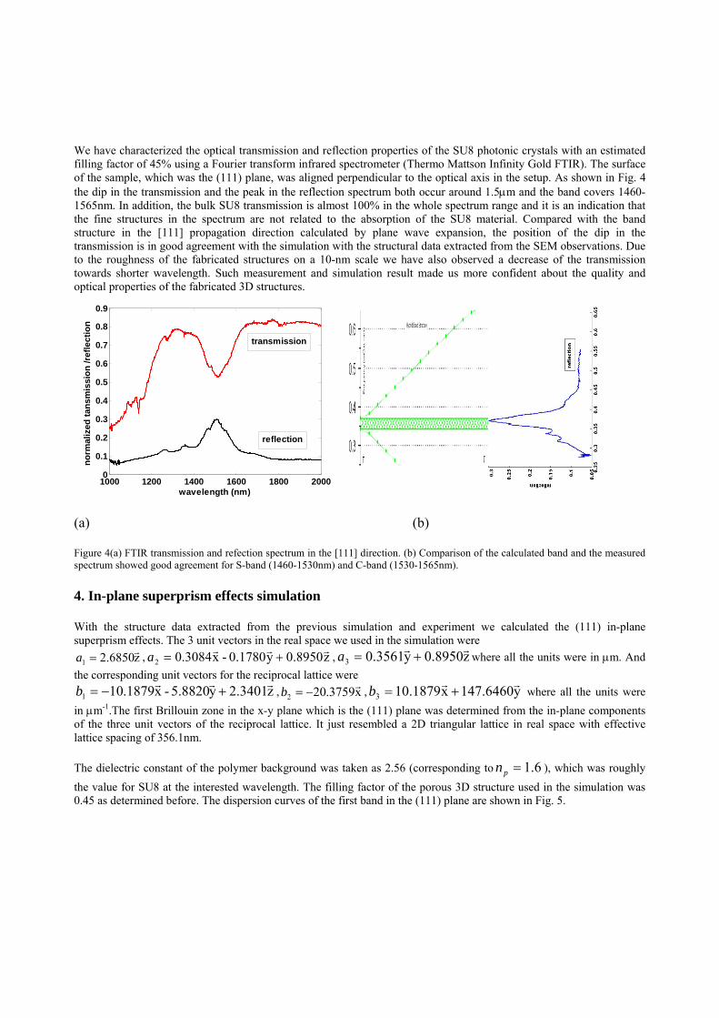
We have characterized the optical transmission and reflection properties of the SU8 photonic crystals with an estimated filling factor of 45% using a Fourier transform infrared spectrometer (Thermo Mattson Infinity Gold FTIR). The surface of the sample, which was the (111) plane, was aligned perpendicular to the optical axis in the setup. As shown in Fig. 4 the dip in the transmission and the peak in the reflection spectrum both occur around 1.5μm and the band covers 1460-1565nm. In addition, the bulk SU8 transmission is almost 100% in the whole spectrum range and it is an indication that the fine structures in the spectrum are not related to the absorption of the SU8 material. Compared with the band structure in the [111] propagation direction calculated by plane wave expansion, the position of the dip in the transmission is in good agreement with the simulation with the structural data extracted from the SEM observations. Due to the roughness of the fabricated structures on a 10-nm scale we have also observed a decrease of the transmission towards shorter wavelength. Such measurement and simulation result made us more confident about the quality and optical properties of the fabricated 3D structures.
1000 1200 1400 1600 1800 20000
0.1
0.2
0.3
0.4
0.5
0.6
0.7
0.8
0.9
wavelength (nm)
norm
aliz
ed ta
nsm
issi
on /r
efle
ctio
n
transmission
reflection
(a) (b)
Figure 4(a) FTIR transmission and refection spectrum in the [111] direction. (b) Comparison of the calculated band and the measured spectrum showed good agreement for S-band (1460-1530nm) and C-band (1530-1565nm).
4. In-plane superprism effects simulation With the structure data extracted from the previous simulation and experiment we calculated the (111) in-plane superprism effects. The 3 unit vectors in the real space we used in the simulation were
z2.68501r
=a , z0.8950 y0.1780-x0.30842rrr
+=a , z0.8950 y3561.03rr
+=a where all the units were in μm. And the corresponding unit vectors for the reciprocal lattice were
z2.3401 y5.8820-x1879.101rrr
+−=b , x3759.202r
−=b , y147.6460x1879.103rr
+=b where all the units were in μm-1.The first Brillouin zone in the x-y plane which is the (111) plane was determined from the in-plane components of the three unit vectors of the reciprocal lattice. It just resembled a 2D triangular lattice in real space with effective lattice spacing of 356.1nm. The dielectric constant of the polymer background was taken as 2.56 (corresponding to 6.1=pn ), which was roughly the value for SU8 at the interested wavelength. The filling factor of the porous 3D structure used in the simulation was 0.45 as determined before. The dispersion curves of the first band in the (111) plane are shown in Fig. 5.
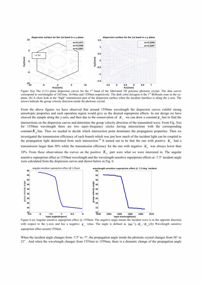
-10 -5 0 5 10-10
-5
0
5
10
Kx(1/um)
Ky(
1/um
)
dispersion surface for the 1st band in x-y plane
w=0.1471w=0.2206w=0.2297
4.5 5 5.5 6 6.5 7
-1.5
-1
-0.5
0
0.5
1
1.5
Kx(1/um)
Ky(
1/um
)
dispersion surface for the 1st band in x-y plane
w=0.2206w=0.2297
Figure 5(a) The (111) plane dispersion curves for the 1st band of the fabricated 3D polymer photonic crystal. The data curves correspond to wavelengths of 2421nm, 1614nm and 1550nm respectively. The dark color hexagon is the 1st Brillouin zone in the xy- plane. (b) A close look at the “high” transmission part of the dispersion surface when the incident interface is along the y-axis. The arrows indicate the group velocity direction inside the photonic crystal. From the above figures we have observed that around 1550nm wavelength the dispersion curves exhibit strong anisotropic properties and such operation region would give us the desired superprsim effects. In our design we have cleaved the sample along the y-axis, and then due to the conservation of ⊥K we can draw a constant yK line to find the intersections on the dispersion curves and determine the group velocity direction of the transmitted wave. From Fig. 5(a) for 1550nm wavelength there are two equiv-frequency circles having intersections with the corresponding constant yK line. Thus we needed to decide which intersection point dominates the propagation properties. Then we investigated the transmission efficiency of each branch which was just how much of the incident light can be coupled to the propagation light determined from each intersection.20 It turned out to be that the one with positive xK had a
transmission larger than 50% while the transmission efficiency for the one with negative xK was always lower than
10%. From these observations the curves on the positive xK part were what we were interested in. The angular sensitive superprism effect at 1550nm wavelength and the wavelength sensitive superprism effects at -7.3° incident angle were calculated from the dispersion curves and shown below in Fig. 6.
-8.5 -8 -7.5 -7 -6.5 -615
20
25
30
35
40
45
50
55
60
input angle(degree)
grou
p ve
loci
ty a
ngle
angular sensitive superprism effect @ 1.55um
1545 1550 1555 1560 1565 157010
15
20
25
30
35
40
45
50
55
input wavlength(nm)
grou
p ve
loci
ty a
ngle
wavelength sensitive superprism effect @ -7.3 deg incident
Figure 6 (a) Angular sensitive superprism effect @ 1550nm. The negative angle means the incident wave is in the opposite direction with respect to the y-axis and has a negative
yK value. The angle is defined as )/(tan 1yx KK−− (b) Wavelength sensitive
superprism effect around 1550nm. When the incident angle changes from -7.5° to -7°, the propagation angle inside the photonic crystal changes from 56° to 21° . And when the wavelength changes from 1555nm to 1559nm, there is a dramatic change of the propagation angle
1stt BZ
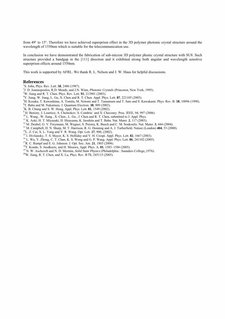
from 49° to 15°. Therefore we have achieved superprism effect in the 3D polymer photonic crystal structure around the wavelength of 1550nm which is suitable for the telecommunication use.
In conclusion we have demonstrated the fabrication of sub-micron 3D polymer phonic crystal structure with SU8. Such structure provided a bandgap in the [111] direction and it exhibited strong both angular and wavelength sensitive superprism effects around 1550nm. This work is supported by AFRL. We thank R. L. Nelson and J. W. Haus for helpful discussions. References 1S. John, Phys. Rev. Lett. 58, 2486 (1987). 2J. D. Joannopoulos, R.D. Meade, and J.N. Winn, Photonic Crystals (Princeton, New York, 1995). 3W. Jiang and R. T. Chen. Phys. Rev. Lett. 91, 213901 (2003). 4Y. Jiang, W. Jiang, L. Gu, X. Chen and R. T. Chen. Appl. Phys. Lett. 87, 221105 (2005). 5H. Kosaka, T. Kawashima, A. Tomita, M. Notomi and T. Tamamura and T. Sato and S. Kawakami. Phys. Rev. B. 58, 10096 (1998). 6T. Baba and M. Nakamura. J. Quantum Electron. 38, 909 (2002). 7K. B. Chung and S. W. Hong, Appl. Phys. Lett. 81, 1549 (2002). 9 H. Benisty, J. Lourtioz, A. Chelnokov, S. Combrie´ and X. Checoury. Proc. IEEE, 94, 997 (2006). 10 L. Wang , W. Jiang , X. Chen , L. Gu , J. Chen and R. T. Chen, submitted to J. Appl. Phys. 11 K. Aoki, H. T. Miyazaki, H. Hirayama, K. Inoshita and T. Baba. Nat. Mater. 2, 117 (2003). 12 M. Deubel, G. V. Freymann, M. Wegner, S. Pereira, K. Busch and C. M. Soukoulis. Nat. Mater. 3, 444 (2004). 13 M. Campbell, D. N. Sharp, M. T. Harrison, R. G. Denning and A. J. Turberfield. Nature (London) 404, 53 (2000). 14L. Z. Cai, X. L. Yang and Y. R. Wang. Opt. Lett. 27, 900, (2002). 15 I. Divliansky, T. S. Mayer, K. S. Holliday and V. H. Crespi. Appl. Phys. Lett. 82, 1667 (2003). 16 L. Wu, Y. Zhong, C. T. Chan, K. S. Wong and G. P. Wang. Appl. Phys. Lett. 86, 241102 (2005). 17R. C. Rumpf and E. G. Johnson. J. Opt. Soc. Am. 21, 1803 (2004). 18T. Kondo, S. Juodkazis, and H. Misawa, Appl. Phys. A. 81, 1583–1586 (2005). 19 N. W. Aschcroft and N. D. Mermin, Solid State Physics (Philadelphia : Saunders College,,1976). 20W. Jiang, R. T. Chen, and X. Lu, Phys. Rev. B 71, 245115 (2005).
Related Documents