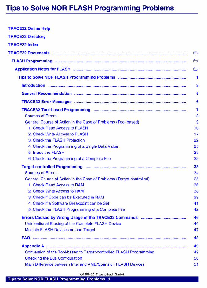
Tips to Solve NOR FLASH Programming Problems 1 ©1989-2017 Lauterbach GmbH Tips to Solve NOR FLASH Programming Problems TRACE32 Online Help TRACE32 Directory TRACE32 Index TRACE32 Documents ...................................................................................................................... FLASH Programming .................................................................................................................... Application Notes for FLASH .................................................................................................... Tips to Solve NOR FLASH Programming Problems ............................................................ 1 Introduction .......................................................................................................................... 3 General Recommendation ................................................................................................... 5 TRACE32 Error Messages ................................................................................................... 6 TRACE32 Tool-based Programming .................................................................................. 7 Sources of Errors 8 General Course of Action in the Case of Problems (Tool-based) 9 1. Check Read Access to FLASH 10 2. Check Write Access to FLASH 17 3. Check the FLASH Protection 22 4. Check the Programming of a Single Data Value 25 5. Erase the FLASH 29 6. Check the Programming of a Complete File 32 Target-controlled Programming ......................................................................................... 33 Sources of Errors 34 General Course of Action in the Case of Problems (Target-controlled) 35 1. Check Read Access to RAM 36 2. Check Write Access to RAM 38 3. Check if Code can be Executed in RAM 39 4. Check if a Software Breakpoint can be Set 41 5. Check the FLASH Programming of a Complete File 42 Errors Caused by Wrong Usage of the TRACE32 Commands ........................................ 46 Unintentional Erasing of the Complete FLASH Device 46 Multiple FLASH Devices on one Target 47 FAQ ........................................................................................................................................ 48 Appendix A ........................................................................................................................... 49 Conversion of the Tool-based to Target-controlled FLASH Programming 49 Checking the Bus Configuration 50 Main Difference between Intel and AMD/Spansion FLASH Devices 51

Welcome message from author
This document is posted to help you gain knowledge. Please leave a comment to let me know what you think about it! Share it to your friends and learn new things together.
Transcript
Tips to Solve NOR FLASH Programming Problems
TRACE32 Online Help
TRACE32 Directory
TRACE32 Index
TRACE32 Documents ......................................................................................................................
FLASH Programming ....................................................................................................................
Application Notes for FLASH ....................................................................................................
Tips to Solve NOR FLASH Programming Problems ............................................................ 1
Introduction .......................................................................................................................... 3
General Recommendation ................................................................................................... 5
TRACE32 Error Messages ................................................................................................... 6
TRACE32 Tool-based Programming .................................................................................. 7
Sources of Errors 8
General Course of Action in the Case of Problems (Tool-based) 9
1. Check Read Access to FLASH 10
2. Check Write Access to FLASH 17
3. Check the FLASH Protection 22
4. Check the Programming of a Single Data Value 25
5. Erase the FLASH 29
6. Check the Programming of a Complete File 32
Target-controlled Programming ......................................................................................... 33
Sources of Errors 34
General Course of Action in the Case of Problems (Target-controlled) 35
1. Check Read Access to RAM 36
2. Check Write Access to RAM 38
3. Check if Code can be Executed in RAM 39
4. Check if a Software Breakpoint can be Set 41
5. Check the FLASH Programming of a Complete File 42
Errors Caused by Wrong Usage of the TRACE32 Commands ........................................ 46
Unintentional Erasing of the Complete FLASH Device 46
Multiple FLASH Devices on one Target 47
FAQ ........................................................................................................................................ 48
Appendix A ........................................................................................................................... 49
Conversion of the Tool-based to Target-controlled FLASH Programming 49
Checking the Bus Configuration 50
Main Difference between Intel and AMD/Spansion FLASH Devices 51
Tips to Solve NOR FLASH Programming Problems 1 ©1989-2017 Lauterbach GmbH

Intel FLASH Devices 52
Switch to ID-Mode (Intel) 52
Status Analysis (Intel) 54
AMD/Spansion FLASH Devices 56
Switch to ID-Mode (AMD/Spansion) 56
Switch to CFI Mode (AMD/Spansion) 58
The SYStem.LOG.List Command 60
Interpretation of the SYStem.LOG.List 62
Error Scenarios 67
Appendix B ........................................................................................................................... 68
FLASH Width BYTE 68
FLASH Width WORD 69
FLASH Width LONG 70
FLASH Width QUAD 72
Tips to Solve NOR FLASH Programming Problems 2 ©1989-2017 Lauterbach GmbH
Tips to Solve NOR FLASH Programming Problems
Version 06-Nov-2017
Introduction
The goal of this manual is to provide tips to solve problems that might arise while programming off-chip NOR FLASHs by TRACE32.
An introduction to the FLASH programming can be found in the “Onchip/NOR FLASH Programming User’s Guide” (norflash.pdf).
For a complete list of all FLASH programming commands refer to the FLASH command group.
Nearly all off-chip NOR FLASHs can be programmed via:
• TRACE32 tool-based FLASH programming
• target-controlled FLASH programming
Tips to Solve NOR FLASH Programming Problems 3 ©1989-2017 Lauterbach GmbH
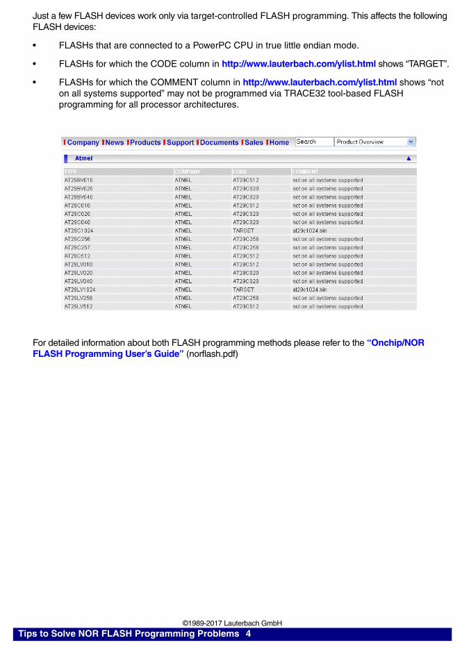
Just a few FLASH devices work only via target-controlled FLASH programming. This affects the following FLASH devices:
• FLASHs that are connected to a PowerPC CPU in true little endian mode.
• FLASHs for which the CODE column in http://www.lauterbach.com/ylist.html shows “TARGET”.
• FLASHs for which the COMMENT column in http://www.lauterbach.com/ylist.html shows “not on all systems supported” may not be programmed via TRACE32 tool-based FLASH programming for all processor architectures.
For detailed information about both FLASH programming methods please refer to the “Onchip/NOR FLASH Programming User’s Guide” (norflash.pdf)
Tips to Solve NOR FLASH Programming Problems 4 ©1989-2017 Lauterbach GmbH

General Recommendation
If you start with a new FLASH device, it is recommended to set up a script that uses TRACE32 tool-based FLASH programming first. Errors are less likely with this method because less target resources are required.
If the script that uses TRACE32 tool-based FLASH programming runs faultless, you can almost be sure that:
• The FLASH declaration is correct
• The bus configuration registers for the FLASH devices are set up correctly
• The interface between the CPU and the FLASH devices on your target hardware works faultless
• TRACE32 can erase and program the FLASH devices correctly
After TRACE32 tool-based FLASH programming works correctly, you can convert this script to a target-controlled FLASH programming script. This is advisable because target-controlled FLASH programming is much faster. Refer to “Conversion of the Tool-based to Target-controlled FLASH Programming” in Tips to Solve NOR FLASH Programming Problems, page 49 (flash_diagnosis.pdf) for details.
Tips to Solve NOR FLASH Programming Problems 5 ©1989-2017 Lauterbach GmbH

TRACE32 Error Messages
One of the following error messages is displayed, when a FLASH erasing/programming error occurs:
For target-controlled FLASH programming the following error message may be displayed:
TRACE32 Error Messages
programming error Error in programming the FLASH. Proceed as described in “General Course of Action in the Case of Problems (Tool-based)” in Tips to Solve NOR FLASH Programming Problems, page 9 (flash_diagnosis.pdf).
erase error Error in erasing the FLASH. Proceed as described in “General Course of Action in the Case of Problems (Tool-based)” in Tips to Solve NOR FLASH Programming Problems, page 9 (flash_diagnosis.pdf).
bus error There is no memory at the address range declared for the FLASH. Please check the bus configuration for the FLASH device. Refer to “Checking the Bus Configuration” in Tips to Solve NOR FLASH Programming Problems, page 50 (flash_diagnosis.pdf) for details.
data alignment error
Wrong or incorrect alignment used while writing the FLASH data. It is strongly recommended to use a format option equivalent to the <bus_width> in the FLASH declaration for all write accesses.
FLASH.Crate … Long FLASH.Program ALLData.LOAD.Elf demo.elf /LongFLASH.Program OFF
TRACE32 Error Messages
FLASH algorithm did not execute completely
Proceed as described in “General Course of Action in the Case of Problems (Target-controlled)” in Tips to Solve NOR FLASH Programming Problems, page 35 (flash_diagnosis.pdf).
Make sure that the data cache is switched off, otherwise TRACE32 can not read/update the FLASH status registers.
Tips to Solve NOR FLASH Programming Problems 6 ©1989-2017 Lauterbach GmbH

TRACE32 Tool-based Programming
If TRACE32 tool-based FLASH programming is used, the FLASH algorithm is part of the TRACE32 software and runs on the host.
TRACE32 Software
FLASH algorithm
USB
PowerDebug Module
JTAG Connector
Target
CPU
FLASH
Add
ress
Bus
Dat
a B
us
Con
trol
Lin
es
EBU
EBU=External Bus Unit
on Host
Tips to Solve NOR FLASH Programming Problems 7 ©1989-2017 Lauterbach GmbH

Sources of Errors
CPU Related Errors
• Wrong or incomplete configuration of the bus configuration registers for the FLASH devices
• FLASH area is indicated as cachable and the data cache is on (TRACE32 can not read/update the FLASH status registers)
Errors Related to Address/Data Bus or the Control Lines
• Defect on the data bus (short circuit, broken line, soldering problem …)
• Defect on the address bus (short circuit, broken line, soldering problem …)
• Swapped address or data lines
• Defect on a control line (Chip Select, Output Enable, Write Enable)
Errors Related to the FLASH
• FLASH (sector) is locked
Errors Related to the TRACE32 FLASH Declaration
• Wrong FLASH family code
• Wrong bus width definition
Errors Related to the File that is Programmed
• The file that is programmed unintentionally overwrites peripheral configuration registers
Alignment Error
• Wrong or incorrect alignment used while writing the FLASH data. It is strongly recommended to use a format option for all write accesses that is equivalent to the <bus width> in the FLASH declaration.
FLASH.Create … Long
FLASH.Program ALL
Data.LOAD.Elf demo.elf /Long
FLASH.Program OFF
Tips to Solve NOR FLASH Programming Problems 8 ©1989-2017 Lauterbach GmbH

General Course of Action in the Case of Problems (Tool-based)
In case of FLASH programming problems the following course of actions is recommended:
1. Check the read access toFLASH
2. Check the write access toFLASH
3. Check the FLASH protection
4. Check the FLASH programmingof a single data value
5. Erase the FLASH
6. Check the FLASH programmingof a complete file
Tips to Solve NOR FLASH Programming Problems 9 ©1989-2017 Lauterbach GmbH
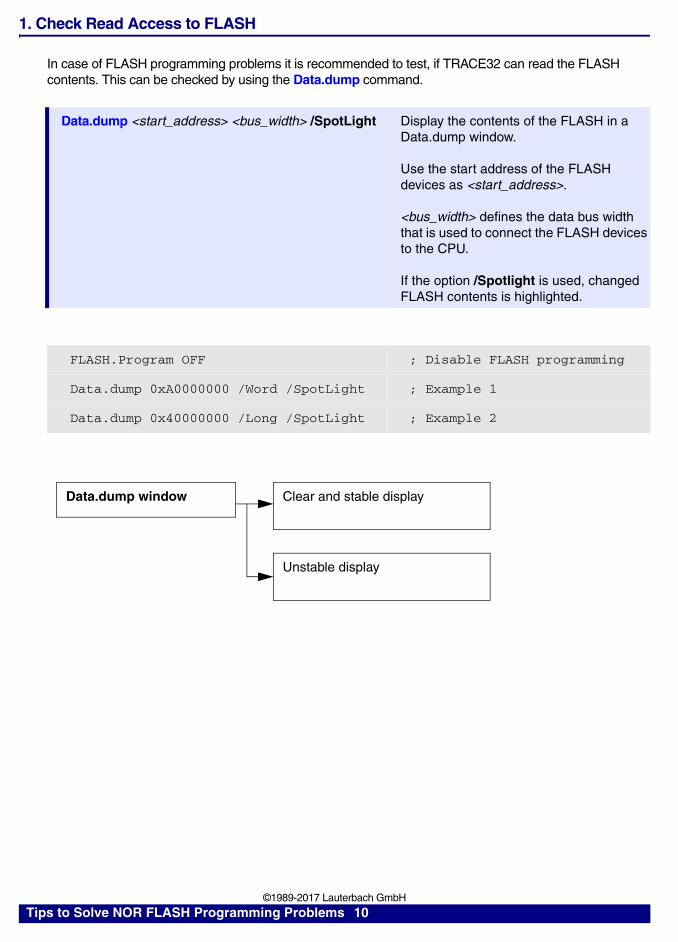
1. Check Read Access to FLASH
In case of FLASH programming problems it is recommended to test, if TRACE32 can read the FLASH contents. This can be checked by using the Data.dump command.
Data.dump <start_address> <bus_width> /SpotLight Display the contents of the FLASH in a Data.dump window.
Use the start address of the FLASH devices as <start_address>.
<bus_width> defines the data bus width that is used to connect the FLASH devices to the CPU.
If the option /Spotlight is used, changed FLASH contents is highlighted.
FLASH.Program OFF ; Disable FLASH programming
Data.dump 0xA0000000 /Word /SpotLight ; Example 1
Data.dump 0x40000000 /Long /SpotLight ; Example 2
Data.dump window Clear and stable display
Unstable display
Tips to Solve NOR FLASH Programming Problems 10 ©1989-2017 Lauterbach GmbH
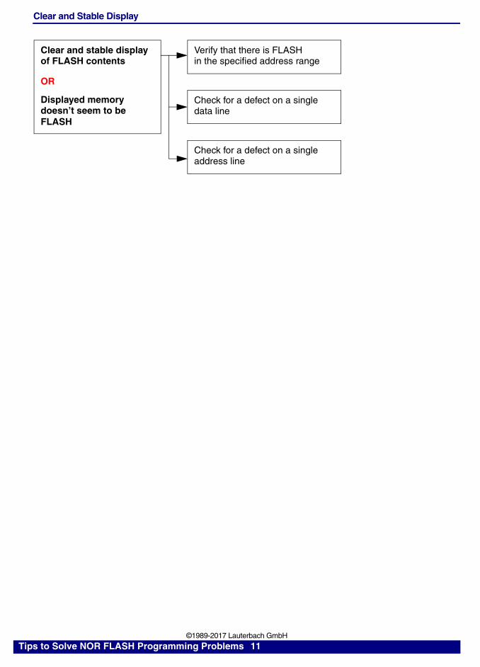
Clear and Stable Display
Clear and stable display of FLASH contents
Verify that there is FLASH in the specified address range
Check for a defect on a singledata line
Check for a defect on a singleaddress line
Displayed memory doesn’t seem to beFLASH
OR
Tips to Solve NOR FLASH Programming Problems 11 ©1989-2017 Lauterbach GmbH

1. Verify that the specified address range is FLASH
Here an example of how to verify if there is FLASH at the specified address range:
This test can have the following results:
If the result is No memory:
- Please check the bus configuration registers. For details refer to “Checking the Bus Configuration” in Tips to Solve NOR FLASH Programming Problems, page 50 (flash_diagnosis.pdf).
- Please check your target for hardware problems accessing the off-chip FLASH.
If the result is RAM:
- Please check the bus configuration registers. For details refer to “Checking the Bus Configuration” in Tips to Solve NOR FLASH Programming Problems, page 50 (flash_diagnosis.pdf).
- Please check your target design for the correct FLASH address range.
Short description and link to newly introduced command:
FLASH.Program OFF ; Disable FLASH programming
Data.TestList 0xa1000000++3fffff ; Check memory type located at; the specified address range.; It is recommended to specify; the complete FLASH address; space.
ok RAM
read only FLASH / ROM
read fail write fail
No memory
Data.TestList <address_range> Test memory type for specified address range
The memory test stays active as long as the Data.TestList window is displayed.
Tips to Solve NOR FLASH Programming Problems 12 ©1989-2017 Lauterbach GmbH
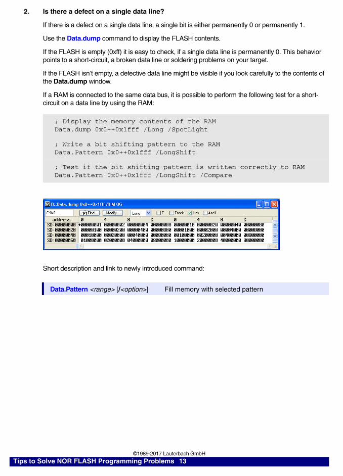
2. Is there a defect on a single data line?
If there is a defect on a single data line, a single bit is either permanently 0 or permanently 1.
Use the Data.dump command to display the FLASH contents.
If the FLASH is empty (0xff) it is easy to check, if a single data line is permanently 0. This behavior points to a short-circuit, a broken data line or soldering problems on your target.
If the FLASH isn’t empty, a defective data line might be visible if you look carefully to the contents of the Data.dump window.
If a RAM is connected to the same data bus, it is possible to perform the following test for a short-circuit on a data line by using the RAM:
Short description and link to newly introduced command:
; Display the memory contents of the RAMData.dump 0x0++0x1fff /Long /SpotLight
; Write a bit shifting pattern to the RAMData.Pattern 0x0++0x1fff /LongShift
; Test if the bit shifting pattern is written correctly to RAMData.Pattern 0x0++0x1fff /LongShift /Compare
Data.Pattern <range> [/<option>] Fill memory with selected pattern
Tips to Solve NOR FLASH Programming Problems 13 ©1989-2017 Lauterbach GmbH

3. Is there a defect on a single address line?
A defective address line results in mirrored memory. This effect is only visible in the Data.dump window, if the FLASH is not empty.
Mirrored address ranges can be found by the following procedure:
Please be aware, that one reason for mirrored address ranges can also be a wrong bus configuration for the FLASH device.
&start_address=0x40000000
&flash_size=0x3fffff
; display a hex dump Data.dump &start_address /Long
; store the contents of the first four 32-bit values into PRACTICE; variables to build a test pattern&v1=Data.Long(D:&start_address)
&v2=Data.Long(D:&start_address+0x4)
&v3=Data.Long(D:&start_address+0x8)
&v4=Data.Long(D:&start_address+0xc)
; search for the test pattern in the FLASHData.Find (&start_address+0x10)++&flash_size %Long &v1 &v2 &v3 &v4
IF FOUND()
; if the test pattern is found in the FLASH, lock carefully to; the Data.dump window to check if this is a result of mirrored; address rangesData.dump TRACK.ADDRESS() /Long
ENDDO
Mirrored address range
Tips to Solve NOR FLASH Programming Problems 14 ©1989-2017 Lauterbach GmbH

Short description and link to newly introduced command:
Data.Find <range> %<format> <test_pattern> FOUND() returns true if the <test_pattern> was foundTRACK.ADDRESS() returns the address at which the <test_pattern> was found
Tips to Solve NOR FLASH Programming Problems 15 ©1989-2017 Lauterbach GmbH
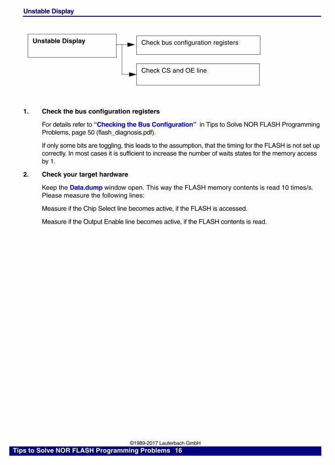
Unstable Display
1. Check the bus configuration registers
For details refer to “Checking the Bus Configuration” in Tips to Solve NOR FLASH Programming Problems, page 50 (flash_diagnosis.pdf).
If only some bits are toggling, this leads to the assumption, that the timing for the FLASH is not set up correctly. In most cases it is sufficient to increase the number of waits states for the memory access by 1.
2. Check your target hardware
Keep the Data.dump window open. This way the FLASH memory contents is read 10 times/s. Please measure the following lines:
Measure if the Chip Select line becomes active, if the FLASH is accessed.
Measure if the Output Enable line becomes active, if the FLASH contents is read.
Unstable Display Check bus configuration registers
Check CS and OE line
Tips to Solve NOR FLASH Programming Problems 16 ©1989-2017 Lauterbach GmbH

2. Check Write Access to FLASH
A simple way to check if TRACE32 has write access to the FLASH is to switch the FLASH into ID-mode (Autoselect Mode for AMD/Spansion devices, Read Identifier Mode for Intel devices).
In ID-mode the following information is provided:
• Manufacturer identification
• Device identification
• Sector protection information if available
Intel FLASH Devices
The procedure to switch to ID-mode is described in “Switch to ID-Mode (Intel)” in Tips to Solve NOR FLASH Programming Problems, page 52 (flash_diagnosis.pdf).
Alternative test procedures:
• Try to read the FLASH status and reset the status registers. For details refer to “Status Analysis (Intel)” in Tips to Solve NOR FLASH Programming Problems, page 54 (flash_diagnosis.pdf). Reading the FLASH status requires less correctly operating address and data lines, but this check is sufficient to test the write access.
AMD/Spansion FLASH Devices
The procedure to switch to ID-mode is described in “Switch to ID-Mode (AMD/Spansion)” in Tips to Solve NOR FLASH Programming Problems, page 56 (flash_diagnosis.pdf).
Alternative test procedures:
• Try to switch to CFI mode for Intel/AMD FLASH devices, if CFI mode is supported by your FLASH device. For details refer to “Switch to CFI Mode (AMD/Spansion)” in Tips to Solve NOR FLASH Programming Problems, page 58 (flash_diagnosis.pdf). Switching to CFI mode requires less correctly operating address and data lines, but this check is sufficient to test the write access.
Tips to Solve NOR FLASH Programming Problems 17 ©1989-2017 Lauterbach GmbH
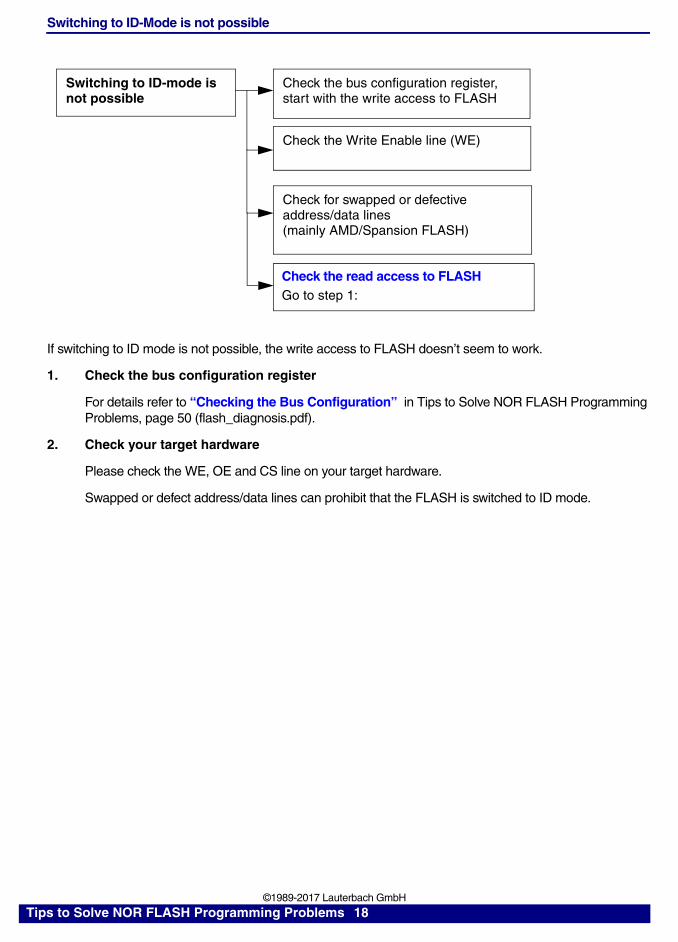
Switching to ID-Mode is not possible
If switching to ID mode is not possible, the write access to FLASH doesn’t seem to work.
1. Check the bus configuration register
For details refer to “Checking the Bus Configuration” in Tips to Solve NOR FLASH Programming Problems, page 50 (flash_diagnosis.pdf).
2. Check your target hardware
Please check the WE, OE and CS line on your target hardware.
Swapped or defect address/data lines can prohibit that the FLASH is switched to ID mode.
Switching to ID-mode isnot possible
Check the bus configuration register,
Check the Write Enable line (WE)
start with the write access to FLASH
Check for swapped or defectiveaddress/data lines (mainly AMD/Spansion FLASH)
Go to step 1:Check the read access to FLASH
Tips to Solve NOR FLASH Programming Problems 18 ©1989-2017 Lauterbach GmbH

The Manufacturer Identification or the Device Identifier is wrong
1. Is there a defect on an address line?
A defective address line results in mirrored memory. This effect is only visible in the Data.dump window, if the FLASH is not empty.
The manufacturer ID orthe device ID is wrong
Check the bus configuration registers
Check for swapped or defectiveaddress lines
Go to step 1:Check the read access to FLASH
Mirrored address range
Tips to Solve NOR FLASH Programming Problems 19 ©1989-2017 Lauterbach GmbH

Mirrored address ranges can be found by the following procedure:
Please be aware, that one reason for mirrored address ranges can also be a wrong bus configuration for the FLASH device.
For swapped address lines please check your schematics or measure each address line on your target.
Short description and link to newly introduced command:
&start_address=0x40000000
&flash_size=0x3fffff
; display a hex dump Data.dump &start_address /Long
; store the contents of the first four 32-bit values into PRACTICE; variables to build a test pattern&v1=Data.Long(D:&start_address)
&v2=Data.Long(D:&start_address+0x4)
&v3=Data.Long(D:&start_address+0x8)
&v4=Data.Long(D:&start_address+0xc)
; search for the test pattern in the FLASHData.Find (&start_address+0x10)++&flash_size %Long &v1 &v2 &v3 &v4
IF FOUND()
; if the test pattern is found in the FLASH, lock carefully to; the Data.dump window to check if this is a result of mirrored; address rangesData.dump TRACK.ADDRESS() /Long
ENDDO
Data.Find <range> %<format> <test_pattern> FOUND() returns true if the <test_pattern> was found.TRACK.ADDRESS() returns the address at which the <test_pattern> was found.
Tips to Solve NOR FLASH Programming Problems 20 ©1989-2017 Lauterbach GmbH

2. Check the bus configuration registers
For details refer to “Checking the Bus Configuration” in Tips to Solve NOR FLASH Programming Problems, page 50 (flash_diagnosis.pdf).
Tips to Solve NOR FLASH Programming Problems 21 ©1989-2017 Lauterbach GmbH

3. Check the FLASH Protection
The FLASH protection can be checked, if the FLASH is in ID-Mode. For a detailed description on how to switch the FLASH to ID-mode, refer to “2. Check Write Access to FLASH” in Tips to Solve NOR FLASH Programming Problems, page 17 (flash_diagnosis.pdf).
E.g ID information for Intel 28F128W18T:
1st word:Manufacturer ID
0x89 (Intel)
2nd word:Device ID
0x8866 (28F128W18T as bottom boot block device)
3rd word:Sector protection
0x1 (sector locked)
Sector Protection Information
0x0 Sector is not locked
0x1 Sector is locked
any other value Please refer to the data sheet for your FLASH device
Tips to Solve NOR FLASH Programming Problems 22 ©1989-2017 Lauterbach GmbH
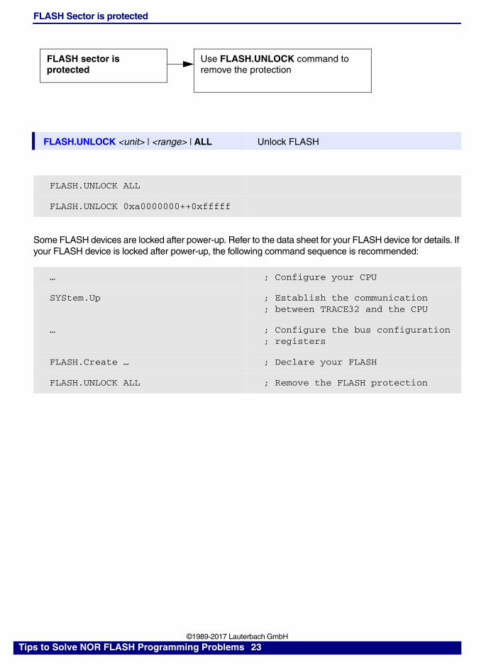
FLASH Sector is protected
Some FLASH devices are locked after power-up. Refer to the data sheet for your FLASH device for details. If your FLASH device is locked after power-up, the following command sequence is recommended:
FLASH.UNLOCK <unit> | <range> | ALL Unlock FLASH
FLASH.UNLOCK ALL
FLASH.UNLOCK 0xa0000000++0xfffff
… ; Configure your CPU
SYStem.Up ; Establish the communication; between TRACE32 and the CPU
… ; Configure the bus configuration; registers
FLASH.Create … ; Declare your FLASH
FLASH.UNLOCK ALL ; Remove the FLASH protection
FLASH sector isprotected
Use FLASH.UNLOCK command toremove the protection
Tips to Solve NOR FLASH Programming Problems 23 ©1989-2017 Lauterbach GmbH
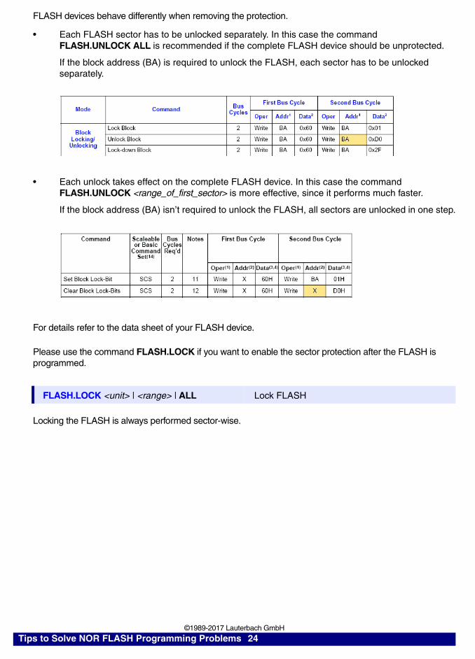
FLASH devices behave differently when removing the protection.
• Each FLASH sector has to be unlocked separately. In this case the command FLASH.UNLOCK ALL is recommended if the complete FLASH device should be unprotected.
If the block address (BA) is required to unlock the FLASH, each sector has to be unlocked separately.
• Each unlock takes effect on the complete FLASH device. In this case the command FLASH.UNLOCK <range_of_first_sector> is more effective, since it performs much faster.
If the block address (BA) isn’t required to unlock the FLASH, all sectors are unlocked in one step.
For details refer to the data sheet of your FLASH device.
Please use the command FLASH.LOCK if you want to enable the sector protection after the FLASH is programmed.
Locking the FLASH is always performed sector-wise.
FLASH.LOCK <unit> | <range> | ALL Lock FLASH
Tips to Solve NOR FLASH Programming Problems 24 ©1989-2017 Lauterbach GmbH
4. Check the Programming of a Single Data Value
Here a short example to program a single data value to FLASH.
; Search for empty FLASH cellData.Find 0x0++0xfffff %Long 0xffffffff
; Display empty cellData.dump TRACK.ADDRESS() /SpotLight
; Enable FLASH programmingFLASH.Program ALL
; Write new data value to empty FLASH cellData.Set TRACK.ADDRESS() %Long 0x01234567
; Disable FLASH programmingFLASH.Program OFF
Data.Find <range> %<format> <test_pattern> FOUND() returns true if the <test_pattern> was found.TRACK.ADDRESS() returns the address at which the <test_pattern> was found.
Tips to Solve NOR FLASH Programming Problems 25 ©1989-2017 Lauterbach GmbH

Programming of a Single Data Value is not Possible
Programming of a singledata value is not possible
Wrong FLASH declaration in TRACE32 (mainly AMD/Spansion)
Defective or swapped data lines
Go to step 2Check the write access to FLASH
Go to step 3Check the FLASH protection
Tips to Solve NOR FLASH Programming Problems 26 ©1989-2017 Lauterbach GmbH

1. Log all read/write accesses that are performed by TRACE32 to write a single data value
If you succeeded to switch the FLASH to ID mode by using the Data.Set commands described in “Switch to ID-Mode (AMD/Spansion)” in Tips to Solve NOR FLASH Programming Problems, page 56 (flash_diagnosis.pdf), perform the following test sequence:
An introduction on how to analyze the logging of the TRACE32 read/write accesses is given in “Interpretation of the SYStem.LOG.List” in Tips to Solve NOR FLASH Programming Problems, page 62 (flash_diagnosis.pdf).
Compare the command register addresses used by TRACE32 with the command register addresses you used to switch to ID-mode. Differences in the command register addresses lead to the assumption that a wrong <family_code> or a wrong <bus_width> is used in the TRACE32 FLASH declaration.
Differences in the endianness used for the data values lead to the assumption that the FLASH is connected to your PowerPC CPU in true little endian mode. In this case only target-controlled FLASH programming can be used.
WinClear
SYStem.LOG.List
FLASH.Program ALL
; Search for empty FLASH cellData.Find 0x++0xfffff %Long 0xffffffff
; Write single data value for empty FLASH cellData.Set TRACK.ADDRESS() %Long 0x01234567
FLASH.Program OFF
Data.Find <range> %<format> <test_pattern> FOUND() returns true if the <test_pattern> was found.TRACK.ADDRESS() returns the address at which the <test_pattern> was found.
Tips to Solve NOR FLASH Programming Problems 27 ©1989-2017 Lauterbach GmbH

2. Is there a defect on a single data line?
To test for a defective data line, write a test pattern to the FLASH.
In case of an error, check your target hardware for a defective data line.
WinClear
FLASH.Program ALL
; Search for an empty FLASH cellData.Find 0x++0xfffff %Long 0xffffffff
; Write test pattern 1Data.Set TRACK.ADDRESS() %Long 0x55555555
; Check the resultData.Print TRACK.ADDRESS() %Long
; Search for the next empty FLASH cellData.Find
; Write test pattern 2Data.Set TRACK.ADDRESS() %Long 0xaaaaaaaa
; Check the resultData.Print TRACK.ADDRESS() %Long
FLASH.Program OFF
Data.Find <range> %<format> <test_pattern> Repeat search by using Data.Find without any parameters.
FOUND() returns true if the <test_pattern> was found.TRACK.ADDRESS() returns the address at which the <test_pattern> was found.
Tips to Solve NOR FLASH Programming Problems 28 ©1989-2017 Lauterbach GmbH
5. Erase the FLASH
Before you try to erase the complete FLASH it is recommended to test if a single FLASH sector can be erased.
Check the protection for a selected FLASH sector as described in “3. Check the FLASH Protection” in Tips to Solve NOR FLASH Programming Problems, page 22 (flash_diagnosis.pdf). Use the following command to erase this single sector.
1. Read the Status Registers for Intel FLASH devices.
Refer to “Status Analysis (Intel)” in Tips to Solve NOR FLASH Programming Problems, page 54 (flash_diagnosis.pdf) for details.
2. Use the SYStem.LOG.List window to check the correct FLASH declaration.
3. Use the SYStem.LOG.List window to check if the data cache is on.
Both test are described in “Interpretation of the SYStem.LOG.List”, page 62.
If TRACE32 is able to erase a single sector, you can be sure, that TRACE32 can erase the complete FLASH.
FLASH.Erase <range> Erase the contents of the specified address range
FLASH.Erase 0x0--0xfffff
Please be aware that TRACE32 doesn’t detect any problem in erasing a FLASH sector, if the FLASH sector is already empty.
FLASH sector can´tbe erased
Wrong FLASH declaration in TRACE32 (mainly AMD/Spansion)
Data cache is on(AMD/Spansion)
Tips to Solve NOR FLASH Programming Problems 29 ©1989-2017 Lauterbach GmbH

Errors that occur now when you try to erase several sectors or the complete FLASH can be isolated as a sector protection problem.
Please be aware that a bulk erase/chip erase command is used to erase the FLASH device if
• bulk erase/chip erase is supported by the FLASH device• and if one of the following commands is used to erase the FLASH
FLASH.Erase ALLFLASH.Erase <unit_number>FLASH.Erase <range>, when the <range> covers the complete address range declared for a <unit_number>
For details refer also to “Unintentional Erasing of the Complete FLASH Device” in Tips to Solve NOR FLASH Programming Problems, page 46 (flash_diagnosis.pdf).
Tips to Solve NOR FLASH Programming Problems 30 ©1989-2017 Lauterbach GmbH

An Erase Error is Generated
Refer to “3. Check the FLASH Protection” in Tips to Solve NOR FLASH Programming Problems, page 22 (flash_diagnosis.pdf) in both cases.
FLASH erase error Use the FLASH.UNLOCK commandto remove the sector protection
Check the protection for each FLASHsector
Tips to Solve NOR FLASH Programming Problems 31 ©1989-2017 Lauterbach GmbH

6. Check the Programming of a Complete File
Unintended Overwrite of Peripheral Configuration Registers
At this point it makes only sense to check if the file you want to program into FLASH unintentionally overwrites peripheral configuration registers.
Here an example, that shows you how to check if your file unintentionally overwrites important configuration registers.
Please make sure, that the file is solely downloaded to the address ranges of the FLASH.
If your file overwrites peripheral configuration registers, please check your map file or continue as follows:
Short description and link to newly introduced command:
Data.LOAD.Elf demo.elf /VM ; Download the file to the virtual; memory
sYmbol.List.Map ; Display the load order and the; address ranges to which the file; was downloaded
FLASH.Program ALL ; Enable FLASH programming
Data.LOAD.Elf demo.elf 0xc00000++0x1ffff ; Load file to FLASH address; ranges
FLASH.Program OFF ; Disable FLASH programming
sYmbol.Map.List Display to which address ranges in the memory a file was downloaded.
Tips to Solve NOR FLASH Programming Problems 32 ©1989-2017 Lauterbach GmbH

Target-controlled Programming
If target-controlled FLASH programming is used, the FLASH algorithm is downloaded to the target RAM and is executed there.
The fact that the FLASH algorithm is downloaded to the target RAM and is executed there adds new requirements:
1. Read and write access to the target RAM by TRACE32
2. Execution of the downloaded FLASH algorithm on the target RAM
3. Setting of software breakpoints to target RAM
TRACE32 Software
USB
PowerDebug Module
JTAG Connector
Target CPU
RAM
Address Bus
Data Bus
Control Lines
EBU
EBU=External Bus Unit
FLASH
FLASH algorithmprogram range
FLASH algorithmdata range
on Host
Tips to Solve NOR FLASH Programming Problems 33 ©1989-2017 Lauterbach GmbH
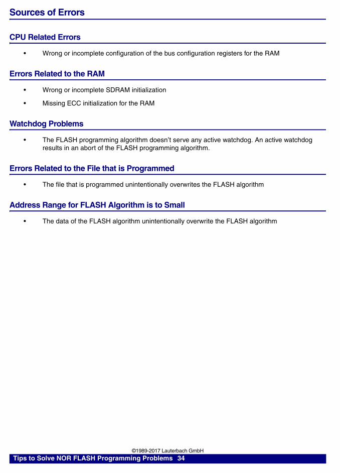
Sources of Errors
CPU Related Errors
• Wrong or incomplete configuration of the bus configuration registers for the RAM
Errors Related to the RAM
• Wrong or incomplete SDRAM initialization
• Missing ECC initialization for the RAM
Watchdog Problems
• The FLASH programming algorithm doesn’t serve any active watchdog. An active watchdog results in an abort of the FLASH programming algorithm.
Errors Related to the File that is Programmed
• The file that is programmed unintentionally overwrites the FLASH algorithm
Address Range for FLASH Algorithm is to Small
• The data of the FLASH algorithm unintentionally overwrite the FLASH algorithm
Tips to Solve NOR FLASH Programming Problems 34 ©1989-2017 Lauterbach GmbH

General Course of Action in the Case of Problems (Target-controlled)
After you defined both, the code range for the FLASH algorithm and the data range for the FLASH algorithm, the following course of action is recommended:
1. Check the read access toRAM
2. Check the write access toRAM
3. Check if code can be executed
4. Check if a software breakpointcan be set to the code in RAM
5. Check the FLASH programmingof a complete file
in RAM
Tips to Solve NOR FLASH Programming Problems 35 ©1989-2017 Lauterbach GmbH
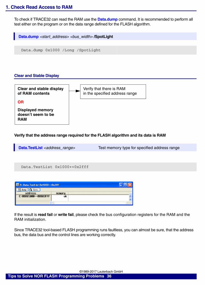
1. Check Read Access to RAM
To check if TRACE32 can read the RAM use the Data.dump command. It is recommended to perform all test either on the program or on the data range defined for the FLASH algorithm.
Clear and Stable Display
Verify that the address range required for the FLASH algorithm and its data is RAM
If the result is read fail or write fail, please check the bus configuration registers for the RAM and the RAM initialization.
Since TRACE32 tool-based FLASH programming runs faultless, you can almost be sure, that the address bus, the data bus and the control lines are working correctly.
Data.dump <start_address> <bus_width> /SpotLight
Data.dump 0x1000 /Long /SpotLight
Data.TestList <address_range> Test memory type for specified address range
Data.TestList 0x1000++0x2fff
Clear and stable display of RAM contents
Verify that there is RAMin the specified address range
Displayed memory doesn’t seem to beRAM
OR
Tips to Solve NOR FLASH Programming Problems 36 ©1989-2017 Lauterbach GmbH

Unstable Display
Unstable Display Check bus configuration registers for the RAM
Tips to Solve NOR FLASH Programming Problems 37 ©1989-2017 Lauterbach GmbH

2. Check Write Access to RAM
To test the write access to RAM, use the following command:
Example:
If TRACE32 can not write to RAM, check the bus configuration registers.
Data.Pattern <range> [/<option>] Fill memory with selected pattern
; Display the memory contents of the RAMData.dump 0x1000 /Long /SpotLight
; Write a bit shifting pattern to the RAMData.Pattern 0x1000++0x2fff /LongShift
; Test if the bit shifting pattern is written correctly to RAMData.Pattern 0x1000++0x2fff /LongShift /Compare
Tips to Solve NOR FLASH Programming Problems 38 ©1989-2017 Lauterbach GmbH

3. Check if Code can be Executed in RAM
To check, if code can be executed use the following command to write a small test program into RAM.
Example:
Data.Assemble <address> <mnemonic> Assemble the mnemonic to RAM
Data.Assemble 0x1000 b 0x1000 ; b 0x1000 prevents that test; program is unintentionally; re-entered after a TRAP or; interrupt
Data.Assemble 0x1002 mov r0,#1 ; Start of test program
Data.Assemble 0x1004 mov r1,#2
Data.Assemble 0x1006 add r2,r1,r0
Data.Assemble 0x1008 b 0x1002
Tips to Solve NOR FLASH Programming Problems 39 ©1989-2017 Lauterbach GmbH

Set the Program Counter/Instruction Pointer to the start address of your test program and perform a few single steps.
Set the Program Counter/Instruction Pointer to the start address of your test program. Start the program execution, let it run for a few seconds and stop it again. With this test you can check if an active watchdog will cause problems for the target-controlled FLASH algorithm.
Please check carefully, if the program execution is stopped within your test program. If this is not case this leads to the assumption, that the watchdog on your target needs to be deactivated.
Register.Set pc 0x1002
Step
Step
Register.Set pc 0x1002
Go
; WAIT 10.s can be used only in scripts
Break
Tips to Solve NOR FLASH Programming Problems 40 ©1989-2017 Lauterbach GmbH

4. Check if a Software Breakpoint can be Set
Check if a software breakpoint can be set to your small test program.
Example:
Break.Set <address> /Program /SOFT Set a software breakpoint to an instruction
Break.Set 0x1004 /Program /SOFT
Go
Tips to Solve NOR FLASH Programming Problems 41 ©1989-2017 Lauterbach GmbH

5. Check the FLASH Programming of a Complete File
Programming of File Failed
FLASH.Create … TARGET … ; Declare your FLASH
FLASH.TARGET …
FLASH.Erase ; Erase the FLASH contents
FLASH.Program ALL ; Enable FLASH programming
Data.LOAD.Elf demo.elf ; Load file to FLASH address ranges
FLASH.Program OFF ; Disable FLASH programming
Data.LOAD.Elf demo.elf /Compare
Programming of filefailed
Check for unintended overwrite ofFLASH algorithm by the fileFLASH algorithm by the file
Check for unintended overwrite ofperipheral configuration registers bythe file
Check for unintended overwrite ofFLASH algorithm by FLASH algorithmdata
Wrong FLASH algorithm is used(wrong bus width or wrong endianness)
Tips to Solve NOR FLASH Programming Problems 42 ©1989-2017 Lauterbach GmbH

1. Does the file that is programmed to the FLASH unintentionally overwrite important configuration registers or parts of the FLASH programming algorithm?
Here an example, that shows you how to check if your file unintentionally overwrites important configuration registers or parts of the FLASH programming algorithm.
Please make sure, that the file is solely downloaded to the address ranges of the FLASH.
If you also want to download some program parts to RAM, please proceed as follows:
Short description and link to newly introduced command:
Data.LOAD.Elf demo.elf /VM ; Download the file to the virtual; memory
sYmbol.List.Map ; Display the load order and the; address ranges to which the file; was downloaded
FLASH.Program ALL ; Enable FLASH; programming
Data.LOAD.Elf demo.elf 0xc00000++0x1ffff ; Load file to FLASH; address ranges
FLASH.Program OFF ; Disable FLASH; programming
Data.LOAD.Elf demo.elf 0xe00000++0x7ff ; Load file to the RAM; address ranges
sYmbol.Map.List Display to which address ranges in memory a file was downloaded.
Tips to Solve NOR FLASH Programming Problems 43 ©1989-2017 Lauterbach GmbH

2. Do the data of the FLASH programming algorithm unintentionally overwrite the FLASH algorithm?
Please make sure, that you reserve enough target RAM for the FLASH programming algorithm. The required size for the FLASH algorithm is calculated as follows:
Required size for the code is size_of(<flash_algorithm>) + 32 byte
The required size for the data of the FLASH algorithm is calculated as follows:
<buffer_size> = size_of(<data_range>) - 32 byte argument buffer - 256 byte stack
<buffer_size> is the maximum number of bytes that are transferred from the TRACE32 software to the external FLASH programming algorithm in one step.
Details on the memory mapping for the FLASH algorithm can be found in the “Onchip/NOR FLASH Programming User’s Guide” (norflash.pdf).
RAM
FLASH algorithmprogram range
FLASH algorithmdata range
The FLASH algorithm data overlaythe FLASH algorithm program range
FLASH algorithm
Figure: Memory mapping for the <code_range>
32 byte
32 byte argument buffer
Figure: Memory mapping for the <data_range>
buffer for programming data
256 byte stack
Tips to Solve NOR FLASH Programming Problems 44 ©1989-2017 Lauterbach GmbH
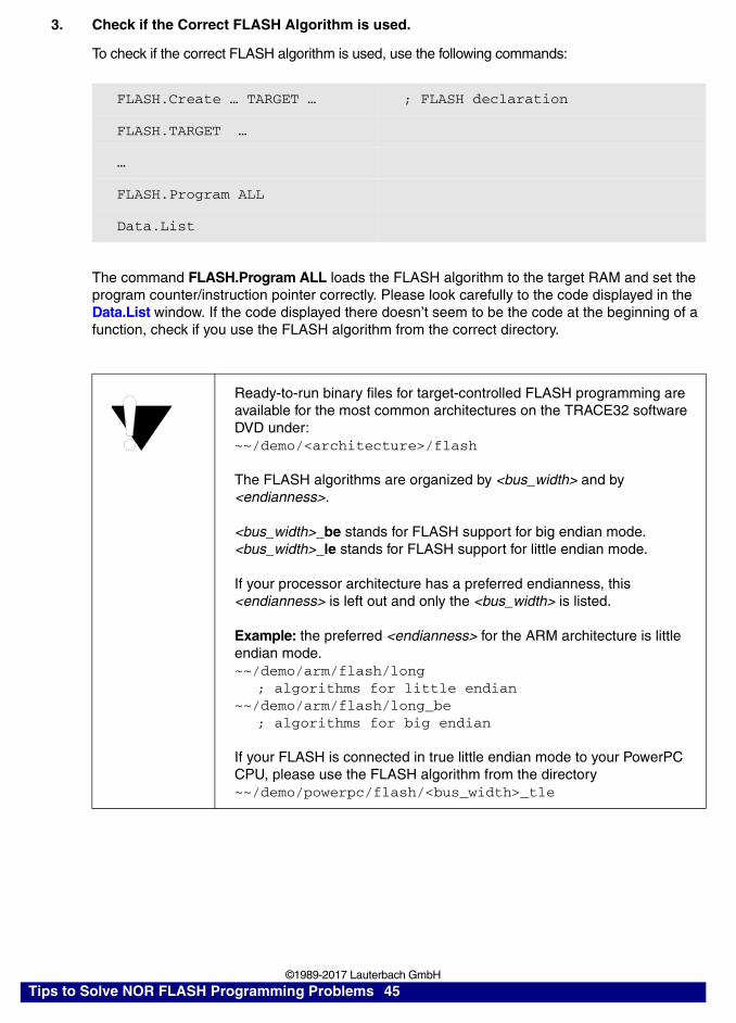
3. Check if the Correct FLASH Algorithm is used.
To check if the correct FLASH algorithm is used, use the following commands:
The command FLASH.Program ALL loads the FLASH algorithm to the target RAM and set the program counter/instruction pointer correctly. Please look carefully to the code displayed in the Data.List window. If the code displayed there doesn’t seem to be the code at the beginning of a function, check if you use the FLASH algorithm from the correct directory.
FLASH.Create … TARGET … ; FLASH declaration
FLASH.TARGET …
…
FLASH.Program ALL
Data.List
Ready-to-run binary files for target-controlled FLASH programming are available for the most common architectures on the TRACE32 software DVD under:~~/demo/<architecture>/flash
The FLASH algorithms are organized by <bus_width> and by <endianness>.
<bus_width>_be stands for FLASH support for big endian mode. <bus_width>_le stands for FLASH support for little endian mode.
If your processor architecture has a preferred endianness, this <endianness> is left out and only the <bus_width> is listed.
Example: the preferred <endianness> for the ARM architecture is little endian mode. ~~/demo/arm/flash/long
; algorithms for little endian~~/demo/arm/flash/long_be
; algorithms for big endian
If your FLASH is connected in true little endian mode to your PowerPC CPU, please use the FLASH algorithm from the directory~~/demo/powerpc/flash/<bus_width>_tle
Tips to Solve NOR FLASH Programming Problems 45 ©1989-2017 Lauterbach GmbH
Errors Caused by Wrong Usage of the TRACE32 Commands
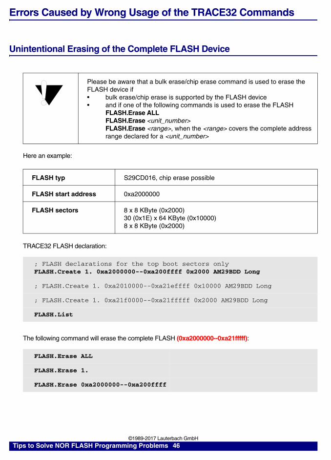
Unintentional Erasing of the Complete FLASH Device
Here an example:
TRACE32 FLASH declaration:
The following command will erase the complete FLASH (0xa2000000--0xa21fffff):
Please be aware that a bulk erase/chip erase command is used to erase the FLASH device if• bulk erase/chip erase is supported by the FLASH device• and if one of the following commands is used to erase the FLASH
FLASH.Erase ALLFLASH.Erase <unit_number>FLASH.Erase <range>, when the <range> covers the complete address range declared for a <unit_number>
FLASH typ S29CD016, chip erase possible
FLASH start address 0xa2000000
FLASH sectors 8 x 8 KByte (0x2000)30 (0x1E) x 64 KByte (0x10000)8 x 8 KByte (0x2000)
; FLASH declarations for the top boot sectors onlyFLASH.Create 1. 0xa2000000--0xa200ffff 0x2000 AM29BDD Long
; FLASH.Create 1. 0xa2010000--0xa21effff 0x10000 AM29BDD Long
; FLASH.Create 1. 0xa21f0000--0xa21fffff 0x2000 AM29BDD Long
FLASH.List
FLASH.Erase ALL
FLASH.Erase 1.
FLASH.Erase 0xa2000000--0xa200ffff
Tips to Solve NOR FLASH Programming Problems 46 ©1989-2017 Lauterbach GmbH
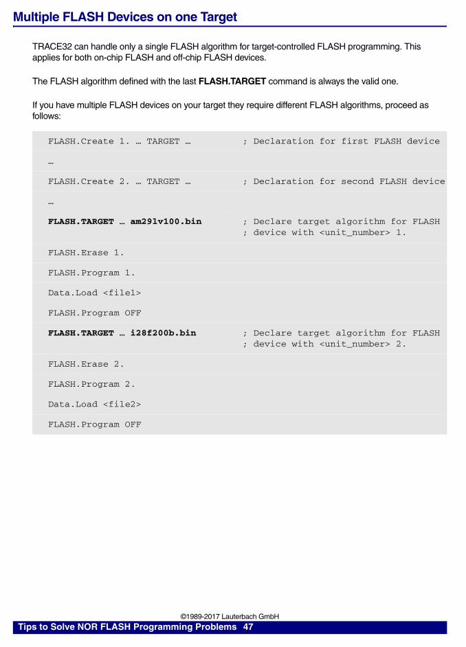
Multiple FLASH Devices on one Target
TRACE32 can handle only a single FLASH algorithm for target-controlled FLASH programming. This applies for both on-chip FLASH and off-chip FLASH devices.
The FLASH algorithm defined with the last FLASH.TARGET command is always the valid one.
If you have multiple FLASH devices on your target they require different FLASH algorithms, proceed as follows:
FLASH.Create 1. … TARGET … ; Declaration for first FLASH device
…
FLASH.Create 2. … TARGET … ; Declaration for second FLASH device
…
FLASH.TARGET … am29lv100.bin ; Declare target algorithm for FLASH; device with <unit_number> 1.
FLASH.Erase 1.
FLASH.Program 1.
Data.Load <file1>
FLASH.Program OFF
FLASH.TARGET … i28f200b.bin ; Declare target algorithm for FLASH; device with <unit_number> 2.
FLASH.Erase 2.
FLASH.Program 2.
Data.Load <file2>
FLASH.Program OFF
Tips to Solve NOR FLASH Programming Problems 47 ©1989-2017 Lauterbach GmbH

FAQ
List of supported FLASH Devices
Ref: 0270
Which FLASH devices are currently supported?
Tips to Solve NOR FLASH Programming Problems 48 ©1989-2017 Lauterbach GmbH
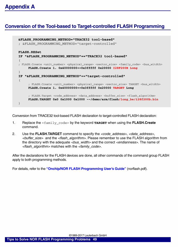
Appendix A
Conversion of the Tool-based to Target-controlled FLASH Programming
Conversion from TRACE32 tool-based FLASH declaration to target-controlled FLASH declaration:
1. Replace the <family_code> by the keyword TARGET when using the FLASH.Create command.
2. Use the FLASH.TARGET command to specify the <code_address>, <data_address>, <buffer_size> and the <flash_algorithm>. Please remember to use the FLASH algorithm from the directory with the adequate <bus_width> and the correct <endianness>. The name of <flash_algorithm> matches with the <family_code>.
After the declarations for the FLASH devices are done, all other commands of the command group FLASH apply to both programming methods.
For details, refer to the “Onchip/NOR FLASH Programming User’s Guide” (norflash.pdf).
&FLASH_PROGRAMMING_METHOD="TRACE32 tool-based"; &FLASH_PROGRAMMING_METHOD="target-controlled"
FLASH.RESetIF "&FLASH_PROGRAMMING_METHOD"=="TRACE32 tool-based"(; FLASH.Create <unit_number> <physical_range> <sector_size> <family_code> <bus_witdth>
FLASH.Create 1. 0x40000000++0x3fffff 0x20000 I28F200B Long )IF "&FLASH_PROGRAMMING_METHOD"=="target-controlled"(
; FLASH.Create <unit_number> <physical_range> <sector_size> TARGET <bus_witdth>
FLASH.Create 1. 0x40000000++0x3fffff 0x20000 TARGET Long
; FLASH.Target <code_address> <data_address> <buffer_size> <flash_algorithm>
FLASH.TARGET 0x0 0x1000 0x1000 ~~/demo/arm/flash/long_be/i28f200b.bin)
Tips to Solve NOR FLASH Programming Problems 49 ©1989-2017 Lauterbach GmbH

Checking the Bus Configuration
Correct settings in the bus configuration registers are key for the FLASH programming. The following settings in the bus configuration are of importance:
• The base address for the FLASH devices
• The size of the FLASH devices
• The bus size that is used to access the FLASH devices
If several FLASH devices are used in parallel to realize the required <bus_width> between the processor and the FLASH memory, make sure that the <bus_width> is configured correctly
• The timing (number of wait states for the access to the FLASH devices)
• The write access has to be enabled for the FLASH devices
Use the PER.view command to check the settings in the bus configuration registers:
Tips to Solve NOR FLASH Programming Problems 50 ©1989-2017 Lauterbach GmbH

Main Difference between Intel and AMD/Spansion FLASH Devices
Intel FLASH Devices
Commands are executed on Intel FLASH devices by writing a specified data value to any FLASH address.
AMD/Spansion FLASH Devices
Commands are executed on AMD/Spansion FLASH devices by writing a command sequence to the command registers of the FLASH.
Example: Switch an AM29BDD with <bus_width> long to ID mode.
Data.Set 0xa0000000 %Long 0x90909090 ; Switch the FLASH device to ID; mode
Data.Set 0xa0000000 %Long 0x70707070 ; Read FLASH status registers
Data.Set 0xa0000000 %Long 0x50505050 ; Reset FLASH status register
Data.Set 0xa0001554 %Long 0xaa
Data.Set 0xa000aa8 %Long 0x55
Data.Set 0xa0001554 %Long 0x90
Tips to Solve NOR FLASH Programming Problems 51 ©1989-2017 Lauterbach GmbH

Intel FLASH Devices
Switch to ID-Mode (Intel)
INTEL FLASH devices are switched to ID mode by writing 0x90 to any address of the FLASH address range.
INTEL FLASH devices are switched back to Read Mode by writing 0xff to any address of the FLASH address range.
Example for FLASH device M58BW016BB from ST Microelectronics. The FLASH device is connected to the CPU via a 32 bit data bus.
ID information:
Data.Set <start_address_of_flash> <bus_width> 0x90
Data.Set <start_address_of_flash> <bus_width> 0xff
Data.Dump 0xa0000000 /Long /NoAscii ; Display the ID mode; information
Data.Set 0xa0000000 %Long 0x90 ; Switch the FLASH device to ID; mode
Manufacturer ID 0x20 (ST Microelectronics)
Device ID 0x8835 (FLASH device M58BW016BB as bottom boot block device)
Tips to Solve NOR FLASH Programming Problems 52 ©1989-2017 Lauterbach GmbH

The ID information is either displayed:
• always at the beginning of each FLASH sector
• repetitive in each FLASH sector (see example above), the repetition rate depends on the FLASH device
Data.Set 0xa0000000 %Long 0xff ; Switch the FLASH back to Read; Mode
Tips to Solve NOR FLASH Programming Problems 53 ©1989-2017 Lauterbach GmbH

Status Analysis (Intel)
Intel FLASH devices can be switched to Read Status Register mode by writing 0x70 to any address of the FLASH.
Any other value then 0x80 indicates an error. For a description of the error codes refer to the data sheet of your FLASH device.
Data.Set <start_address_of_flash> <bus_width> 0x70
Data.Set 0xa0000000 %Long 0x70
Data.dump 0xa0000000 /Long
Tips to Solve NOR FLASH Programming Problems 54 ©1989-2017 Lauterbach GmbH

Writing 0x50 to any address clears the status registers.
Writing 0xff to any address switches the FLASH device back to Read Mode.
Data.dump 0xa0000000 /Long /SpotLight
Data.Set 0xa0000000 %Long 0x50
Data.Set 0xa0000000 %Long 0xff
Tips to Solve NOR FLASH Programming Problems 55 ©1989-2017 Lauterbach GmbH
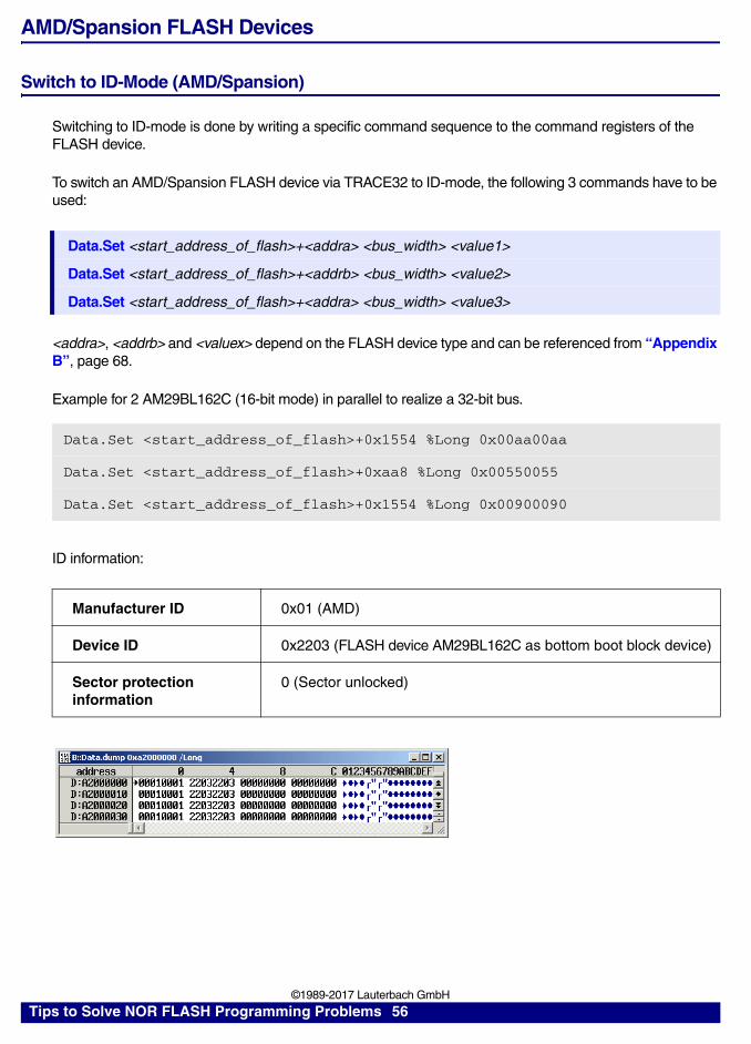
AMD/Spansion FLASH Devices
Switch to ID-Mode (AMD/Spansion)
Switching to ID-mode is done by writing a specific command sequence to the command registers of the FLASH device.
To switch an AMD/Spansion FLASH device via TRACE32 to ID-mode, the following 3 commands have to be used:
<addra>, <addrb> and <valuex> depend on the FLASH device type and can be referenced from “Appendix B”, page 68.
Example for 2 AM29BL162C (16-bit mode) in parallel to realize a 32-bit bus.
ID information:
Data.Set <start_address_of_flash>+<addra> <bus_width> <value1>
Data.Set <start_address_of_flash>+<addrb> <bus_width> <value2>
Data.Set <start_address_of_flash>+<addra> <bus_width> <value3>
Data.Set <start_address_of_flash>+0x1554 %Long 0x00aa00aa
Data.Set <start_address_of_flash>+0xaa8 %Long 0x00550055
Data.Set <start_address_of_flash>+0x1554 %Long 0x00900090
Manufacturer ID 0x01 (AMD)
Device ID 0x2203 (FLASH device AM29BL162C as bottom boot block device)
Sector protection information
0 (Sector unlocked)
Tips to Solve NOR FLASH Programming Problems 56 ©1989-2017 Lauterbach GmbH

The ID information is either displayed:
• always at the beginning of each FLASH sector
• repetitive in each FLASH sector (see example above), the repetition rate depends on the FLASH device
Data.Set <start_address_of_flash> <bus_width> 0xf0 Switch the FLASH back to Read Mode
Data.Set <start_address_of_flash> %Long 0xf0f0f0f0
If switching to ID-mode for an AMD/Spansion device can be done and if the manufacturer-id and the device-id is displayed correctly, you can almost be sure that the data bus is working properly.
Tips to Solve NOR FLASH Programming Problems 57 ©1989-2017 Lauterbach GmbH

Switch to CFI Mode (AMD/Spansion)
To switch an AMD/Spansion FLASH device via TRACE32 to CFI-mode, the following command has to be used:
In the example above 2 16 bit FLASH devices are used in parallel to realize a 32 bit bus. For this reason
is displayed at address 0xa0000040.
Please be aware, that the memory display of QRY will vary depending on:
• the data width of the FLASH device
• the number of parallel FLASH devices
The address 0xa0000040 is also just an example.
Data.Set <start_address_of_flash>+<addra> <bus_width> 0x98
Data.dump <start_address_of_flash> /Long /SpotLight
Data.Set <start_address_of_flash>+0x1554 %Long 0x98989898
0x00510051 Q
0x00520052 R
0x00590059 Y
The letters Q R Y indicate, thatthe FLASH is in CFI mode
Tips to Solve NOR FLASH Programming Problems 58 ©1989-2017 Lauterbach GmbH

Status Analysis (AMD/Spansion)
The operations on AMD/Spansion FLASH devices (e.g. erasing, programming) are initiated by writing a command sequence to the command registers. Since these write accesses are performed by TRACE32, they are not visible to the user by default.
The TRACE32 SYStem.LOG.List window provides now the possibility to log all read and write accesses performed by TRACE32 in order to get full visibility. To restrict the logging to the read/write accesses to the FLASH device, it is recommended to close all TRACE32 windows, that display memory.
By using the SYStem.LOG.List window, you can check the following:
1. Does TRACE32 use the correct addresses for the FLASH command registers?
Wrong command register addresses lead to the assumption, that the wrong <family_code> or the wrong <bus_width> is used in the TRACE32 FLASH declaration.
2. Does TRACE32 write the required data values in the correct endianness to the command registers?
Differences in the endianness used for the data values lead to the assumption that the FLASH is connected to your PowerPC CPU in true little endian mode. In this case only target-controlled FLASH programming can be used.
3. Can TRACE32 read the FLASH status correctly?
If TRACE32 is unable to read the FLASH status, this leads to the assumption, that the data cache is on.
Tips to Solve NOR FLASH Programming Problems 59 ©1989-2017 Lauterbach GmbH

The SYStem.LOG.List Command
The former Data.LOG command is now called SYStem.LOG.List.
Example for TRACE32 screen based logging:
By default the SYStem.LOG.List window can log up to 256 read/write accesses. To log more read/write accesses, define the required size.
SYStem.LOG.List <size> <file> Log all read/write accesses performed by TRACE32.For support purposes it is possible to save the logging to a file.
WinCLEAR ; Close all TRACE32 windows
SYStem.LOG.List ; Open a data log window
… ; Perform your test sequence
WinCLEAR ; Close all TRACE32 windows
SYStem.LOG.List 1000. ; Open a data log window
… ; Perform your test sequence
Tips to Solve NOR FLASH Programming Problems 60 ©1989-2017 Lauterbach GmbH
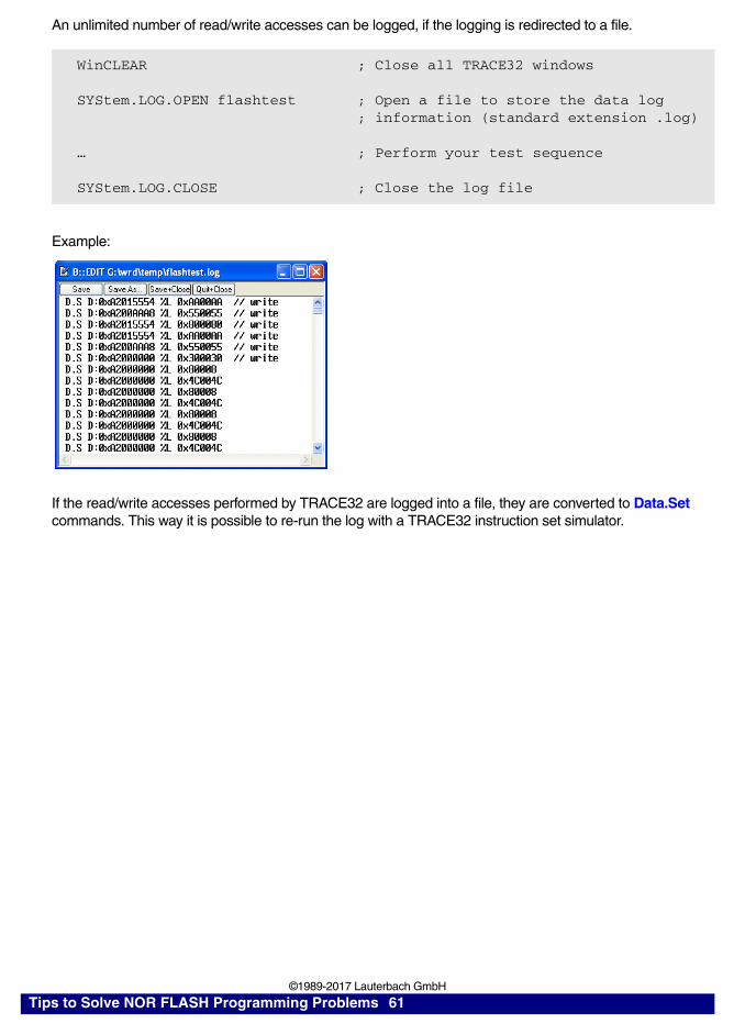
An unlimited number of read/write accesses can be logged, if the logging is redirected to a file.
Example:
If the read/write accesses performed by TRACE32 are logged into a file, they are converted to Data.Set commands. This way it is possible to re-run the log with a TRACE32 instruction set simulator.
WinCLEAR ; Close all TRACE32 windows
SYStem.LOG.OPEN flashtest ; Open a file to store the data log ; information (standard extension .log) … ; Perform your test sequence
SYStem.LOG.CLOSE ; Close the log file
Tips to Solve NOR FLASH Programming Problems 61 ©1989-2017 Lauterbach GmbH

Interpretation of the SYStem.LOG.List
The following shows a step by step interpretation of the TRACE32 read/write accesses logged to the SYStem.LOG.List window.
FLASH configuration: 2 AM29BL162C (16-bit mode) in parallel to realize a 32-bit bus width
Tested FLASH command: Sector erase
1. Check the command register addresses
Please refer to the command definition for the sector erase in the data sheet for your FLASH device.
• TRACE32 uses byte addresses to write to the FLASH command registers. If word addresses are used in the data sheet of the FLASH device, they have to be converted to byte addresses.
• If parallel FLASHs are used to realize the required <bus_width>, this has also to be taken into account:
• Due to compatibility reasons TRACE32 uses 15 bit command register addresses instead of 11.
Calculation example:
FLASH.Create … Long ; FLASH declaration
FLASH.Erase 0xa2000000++0x3fff ; Erase the defined FLASH sector
2 parallel FLASHs Multiply the byte address of the command register by 2
4 parallel FLASHs Multiply the byte address of the command register by 4
Command register address for first bus cycle from data command definition
0x555 (word address)
Conversion from word address to byte address
2 * 0x555 = 0xAAA
Multiplication for parallel FLASHs 2 * 0xAAA = 0x1554
Conversion from 11 bit address into 15 bit command register address
0x15554
Tips to Solve NOR FLASH Programming Problems 62 ©1989-2017 Lauterbach GmbH
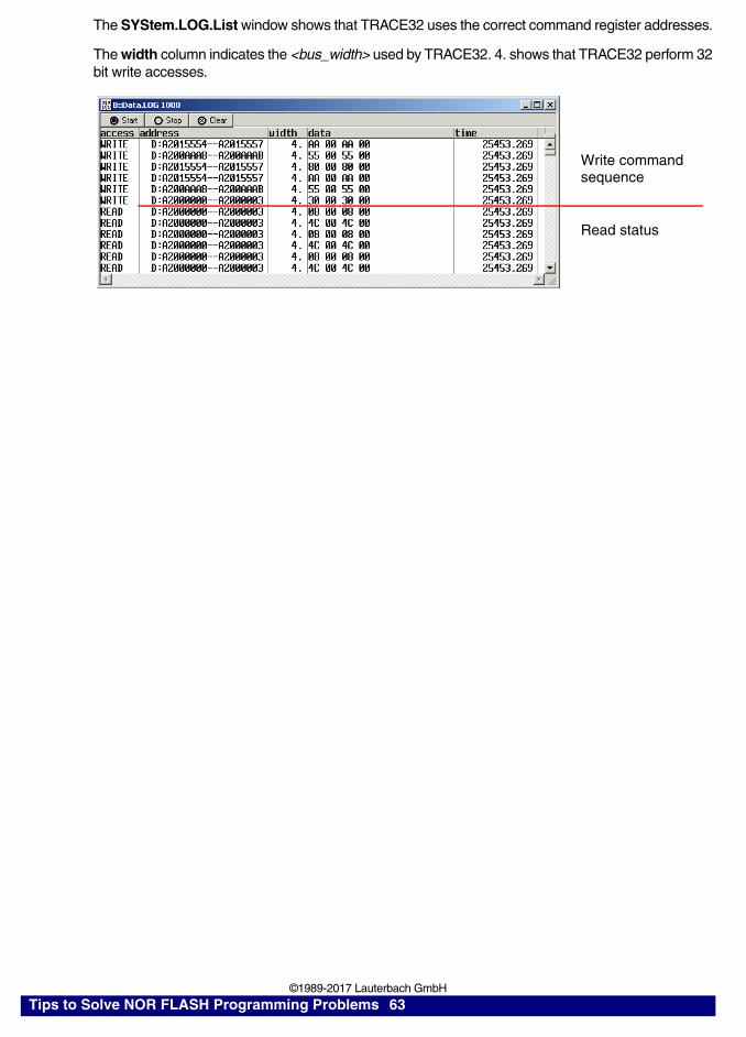
The SYStem.LOG.List window shows that TRACE32 uses the correct command register addresses.
The width column indicates the <bus_width> used by TRACE32. 4. shows that TRACE32 perform 32 bit write accesses.
Write commandsequence
Read status
Tips to Solve NOR FLASH Programming Problems 63 ©1989-2017 Lauterbach GmbH

2. Check the data values
Please refer to the command definition for the sector erase in the data sheet for your FLASH device.
The width column in the SYStem.LOG.List window indicates the <bus_width> used by TRACE32.
The byte order is as follows:
The SYStem.LOG.List window shows that TRACE32 writes the correct data values in little endian mode. Since 2 parallel FLASHs are used, B0 and B2 are used to write the data value.
Byte Order
Little Endian Mode B0 B1 B2 B3
Big Endian Mode B3 B2 B1 B0
Write commandsequence
Read status
Tips to Solve NOR FLASH Programming Problems 64 ©1989-2017 Lauterbach GmbH

3. Check the status read
After TRACE32 wrote the require 6 commands to erase the FLASH sector, it starts reading the FLASH status.
Please refer to the write operation status information in the data sheet for your FLASH device.
The following status bits are of importance:
The following SYStem.LOG.List window show that DQ2 and DQ6 are toggling at each status read.
Status Bits
DQ2/6 Bit 2 and Bit 6 need to toggle at each status read
DQ5 DQ5==1 && DQ7==0 indicates a time-out caused by an internal FLASH error
DQ7 A soon as DQ7 becomes 1, erasing of the FLASH sector is done
Write commandsequence
Read status
Tips to Solve NOR FLASH Programming Problems 65 ©1989-2017 Lauterbach GmbH

The SYStem.LOG.List window below shows that erasing the sector is done (DQ7==1). Afterwards the FLASH is switched back to read mode.
The picture above shows, that the sector erase for one FLASH performed faster (Status already 0xff 0xff).
Read status
Sector erase for both
Write commandto switch FLASHto read mode
FLASH devices is done
Tips to Solve NOR FLASH Programming Problems 66 ©1989-2017 Lauterbach GmbH
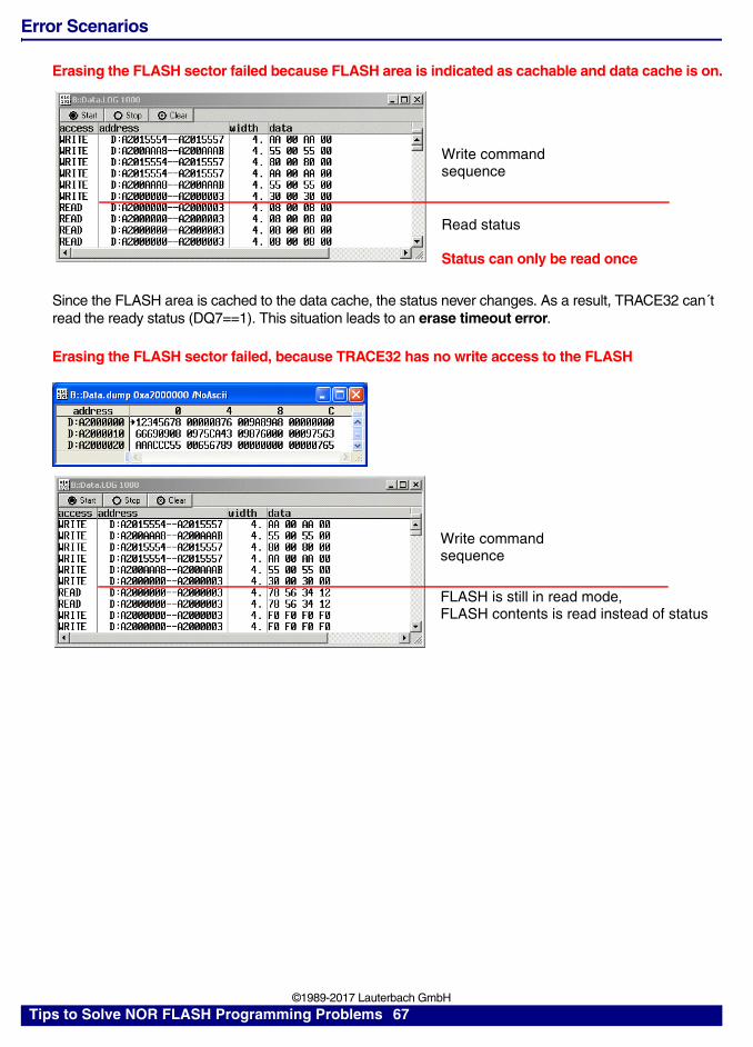
Error Scenarios
Erasing the FLASH sector failed because FLASH area is indicated as cachable and data cache is on.
Since the FLASH area is cached to the data cache, the status never changes. As a result, TRACE32 can´t read the ready status (DQ7==1). This situation leads to an erase timeout error.
Erasing the FLASH sector failed, because TRACE32 has no write access to the FLASH
Write commandsequence
Read status
Status can only be read once
Write commandsequence
FLASH is still in read mode,FLASH contents is read instead of status
Tips to Solve NOR FLASH Programming Problems 67 ©1989-2017 Lauterbach GmbH
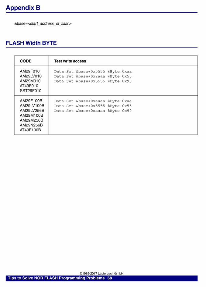
Appendix B
&base=<start_address_of_flash>
FLASH Width BYTE
CODE Test write access
AM29F010AM29LV010AM29M010AT49F010SST29F010
Data.Set &base+0x5555 %Byte 0xaaData.Set &base+0x2aaa %Byte 0x55Data.Set &base+0x5555 %Byte 0x90
AM29F100BAM29LV100BAM29LV256BAM29M100BAM29M256BAM29N256BAT49F100B
Data.Set &base+0xaaaa %Byte 0xaaData.Set &base+0x5555 %Byte 0x55Data.Set &base+0xaaaa %Byte 0x90
Tips to Solve NOR FLASH Programming Problems 68 ©1989-2017 Lauterbach GmbH

FLASH Width WORD
CODE Test write access Test PPC target for truelittle endian mode
AM29F010AM29LV010AM29M010AT49F010SST29F010
D.S &base+0xaaaa %W 0xaaaaD.S &base+0x5554 %W 0x5555D.S &base+0xaaaa %W 0x9090
AM29F100AM29LV100AM29LV256AM29M100AM29M256AM29N256AT49F100
D.S &base+0xaaaa %W 0x00aaD.S &base+0x5554 %W 0x0055D.S &base+0xaaaa %W 0x0090
D.S &base+0xaaaa %W 0xaa00D.S &base+0x5554 %W 0x5500D.S &base+0xaaaa %W 0x9000
AM29F100BAM29LV100BAM29LV256BAM29M100BAM29M256BAM29N256BAT49F100B
D.S &base+0x15554 %W 0xaaaaD.S &base+0xaaaa %W 0x5555D.S &base+0x15554 %W 0x9090
AM29BDDW D.S &base+0x15554 %W 0x00aaD.S &base+0xaaaa %W 0x0055D.S &base+0x15554 %W 0x0090
D.S &base+0x15554 %W 0xaa00D.S &base+0xaaaa %W 0x5500D.S &base+0x15554 %W 0x9000
Tips to Solve NOR FLASH Programming Problems 69 ©1989-2017 Lauterbach GmbH

FLASH Width LONG
CODE
AM29F010AM29LV010AM29M010AT49F010SST29F010
Data.Set &base+0x15554 %Long 0xaaaaaaaaData.Set &base+0xaaa8 %Long 0x55555555Data.Set &base+0x15554 %Long 0x90909090
AM29F100AM29LV100AM29LV256AM29M100AM29M256AM29N256AT49F100
Test write access
Data.Set &base+0x15554 %Long 0x00aa00aaData.Set &base+0xaaa8 %Long 0x00550055Data.Set &base+0x15554 %Long 0x00900090
Test PPC target for true little endian mode
Data.Set &base+0x15554 %Long 0xaa00aa00Data.Set &base+0xaaa8 %Long 0x55005500Data.Set &base+0x15554 %Long 0x90009000
AM29F100BAM29LV100BAM29LV256BAM29M100BAM29M256BAM29N256BAT49F100B
Data.Set &base+0x2aaa8 %Long 0xaaaaaaaaData.Set &base+0x15554 %Long 0x55555555Data.Set &base+0x2aaa8 %Long 0x90909090
AM29BDD Test write access
Data.Set &base+0x15554 %Long 0x000000aaData.Set &base+0xaaa8 %Long 0x00000055Data.Set &base+0x15554 %Long 0x00000090
Test PPC target for true little endian mode
Data.Set &base+0x15554 %Long 0xaa000000Data.Set &base+0xaaa8 %Long 0x55000000Data.Set &base+0x15554 %Long 0x90000000
Tips to Solve NOR FLASH Programming Problems 70 ©1989-2017 Lauterbach GmbH

AM29BDDW Test write access
Data.Set &base+0x2aaa8 %Long 0x00aa00aaData.Set &base+0x15554 %Long 0x00550055Data.Set &base+0x2aaa8 %Long 0x00900090
Test PPC target for true little endian mode
Data.Set &base+0x2aaa8 %Long 0xaa00aa00Data.Set &base+0x15554 %Long 0x55005500Data.Set &base+0x2aaa8 %Long 0x90009000
AM29M2562 Test write access
Data.Set &base+0x15554 %Long 0x0000aaaaData.Set &base+0xaaa8 %Long 0x00005555Data.Set &base+0x15554 %Long 0x00009090
Test PPC target for true little endian mode
Data.Set &base+0x15554 %Long 0xaaaa0000Data.Set &base+0xaaa8 %Long 0x55550000Data.Set &base+0x15554 %Long 0x90900000
CODE
Tips to Solve NOR FLASH Programming Problems 71 ©1989-2017 Lauterbach GmbH
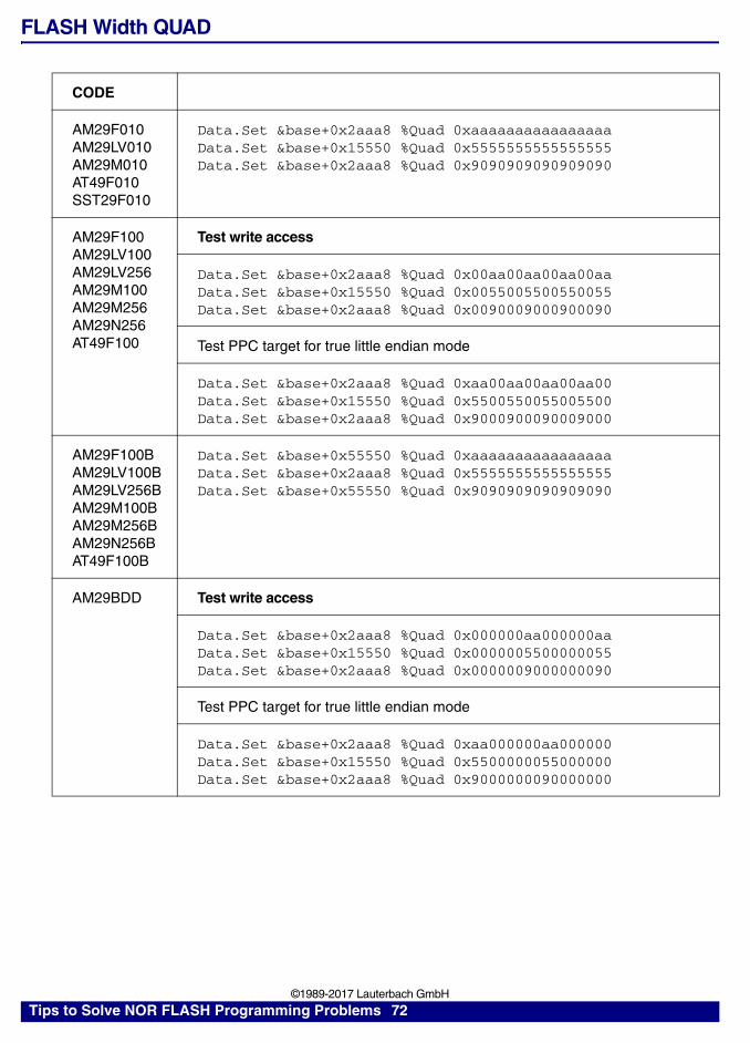
FLASH Width QUAD
CODE
AM29F010AM29LV010AM29M010AT49F010SST29F010
Data.Set &base+0x2aaa8 %Quad 0xaaaaaaaaaaaaaaaaData.Set &base+0x15550 %Quad 0x5555555555555555Data.Set &base+0x2aaa8 %Quad 0x9090909090909090
AM29F100AM29LV100AM29LV256AM29M100AM29M256AM29N256AT49F100
Test write access
Data.Set &base+0x2aaa8 %Quad 0x00aa00aa00aa00aaData.Set &base+0x15550 %Quad 0x0055005500550055Data.Set &base+0x2aaa8 %Quad 0x0090009000900090
Test PPC target for true little endian mode
Data.Set &base+0x2aaa8 %Quad 0xaa00aa00aa00aa00Data.Set &base+0x15550 %Quad 0x5500550055005500Data.Set &base+0x2aaa8 %Quad 0x9000900090009000
AM29F100BAM29LV100BAM29LV256BAM29M100BAM29M256BAM29N256BAT49F100B
Data.Set &base+0x55550 %Quad 0xaaaaaaaaaaaaaaaaData.Set &base+0x2aaa8 %Quad 0x5555555555555555Data.Set &base+0x55550 %Quad 0x9090909090909090
AM29BDD Test write access
Data.Set &base+0x2aaa8 %Quad 0x000000aa000000aaData.Set &base+0x15550 %Quad 0x0000005500000055Data.Set &base+0x2aaa8 %Quad 0x0000009000000090
Test PPC target for true little endian mode
Data.Set &base+0x2aaa8 %Quad 0xaa000000aa000000Data.Set &base+0x15550 %Quad 0x5500000055000000Data.Set &base+0x2aaa8 %Quad 0x9000000090000000
Tips to Solve NOR FLASH Programming Problems 72 ©1989-2017 Lauterbach GmbH

AM29BDDW Test write access
Data.Set &base+0x55550 %Quad 0x00aa00aa00aa00aaData.Set &base+0x2aaa8 %Quad 0x0055005500550055Data.Set &base+0x55550 %Quad 0x0090009000900090
Test PPC target for true little endian mode
Data.Set &base+0x55550 %Quad 0xaa00aa00aa00aa00Data.Set &base+0x2aaa8 %Quad 0x5500550055005500Data.Set &base+0x55550 %Quad 0x9000900090009000
AM29M2562 Test write access
Data.Set &base+0x2aaa8 %Quad 0x0000aaaa0000aaaaData.Set &base+0x15550 %Quad 0x0000555500005555Data.Set &base+0x2aaa8 %Quad 0x0000909000009090
Test PPC target for true little endian mode
Data.Set &base+0x2aaa8 %Quad 0xaaaa0000aaaa0000Data.Set &base+0x15550 %Quad 0x5555000055550000Data.Set &base+0x2aaa8 %Quad 0x9090000090900000
CODE
Tips to Solve NOR FLASH Programming Problems 73 ©1989-2017 Lauterbach GmbH
Related Documents
![Xi31 Sp3 Error Messages Es[1]](https://static.cupdf.com/doc/110x72/5572027d4979599169a39c9d/xi31-sp3-error-messages-es1.jpg)