TDA9105 DEFLECTION PROCESSOR FOR MULTISYNC MONITORS June 1996 PRELIMINARY DATA SHRINK42 (Plastic Package) ORDER CODE : TDA9105 HORIZONTAL . DUAL PLL CONCEPT . 150kHz MAXIMUM FREQUENCY . SELF-ADAPTATIVE . X-RAY PROTECTION INPUT . DC ADJUSTABLE DUTY-CYCLE . 1 st PLL LOCK /UNLOCK INFORMATION . WIDE RANGE DC CONTROLLED H-POSI- TION . ON/OFF SWITCH (FOR PWR MANAGE- MENT) . TWO H-DRIVE POLARITIES . MOIRE OUTPUT VERTICAL . VERTICAL RAMP GENERATOR . 50 TO 165Hz AGC LOOP . DCCONTROLLED V-AMP, V-POS, S-AMP & C-COR . ON/OFF SWITCH EWPCC . VERTICAL PARABOLA GENERATOR WITH DC CONTROLLED KEYSTONE & AMPLITUDE . AUTO TRACKING WITH V-POS & V-AMP GEOMETRY . WAVE FORM GENERATOR FOR PARALEL- LOGRAM & SIDE PIN BALANCE CONTROL . AUTO TRACKING WITH V-POS & V-AMP DYNAMIC FOCUS . VERTICAL PARABOLAOUTPUT FOR VERTI- CAL DYNAMIC FOCUS . AUTO TRACKING WITH V-POS & V-AMP GENERAL . ACCEPT POSITIVE OR NEGATIVE HORI- ZONTAL& VERTICAL SYNC POLARITIES . SEPARATE H & V TTL INPUT . COMPOSITE BLANKING OUTPUT 1 2 3 4 5 6 7 8 9 10 11 12 42 41 40 39 38 37 36 35 34 33 32 31 30 29 28 27 26 25 13 14 15 16 17 18 19 20 21 24 23 22 V-FOCUS H-LOC KOUT P LL2C H-DUTY H-F LY H-G ND H-REF FC2 FC1 C0 R0 P LL1F H-LOC KCAP P LL1INHIB H-POS XRAY-IN H-S YNC V CC GND H-O UTE M H-OUTCOL S P INBAL KEYBAL GEOMOUT EWAMP KEYS T EWOUT V-FLY VDCIN V-S YNC V-POS V-AMP V-OUT C-CORR VS-AMP V-CAP V-RE F V-AGCCAP V-GND MOIRE BLK-OUT VDCO UT 9105-01.EPS PIN CONNECTIONS DESCRIPTION The TDA9105 is a monolithic integrated circuit assembled in a 42 pins shrink dual in line plastic package. This IC controls all the functions related to the horizontal and vertical deflection in multimodes or multisync monitors. This IC, combined with TDA9205 (RGB preamp), STV942x (OSD processor), ST727x (micro control- ler) and TDA817x (vertical booster), allows to real- ize very simple and high quality multimodes or multisync monitors. This is advance information on a new product now in development or undergoing evaluation. Details are subject to change without no tice. 1/32

Welcome message from author
This document is posted to help you gain knowledge. Please leave a comment to let me know what you think about it! Share it to your friends and learn new things together.
Transcript

TDA9105
DEFLECTION PROCESSOR FOR MULTISYNC MONITORS
June 1996
PRELIMINARY DATA
SHRINK42(Plastic Package)
ORDER CODE : TDA9105
HORIZONTAL.DUAL PLL CONCEPT.150kHz MAXIMUM FREQUENCY.SELF-ADAPTATIVE.X-RAY PROTECTION INPUT.DC ADJUSTABLE DUTY-CYCLE.1st PLL LOCK /UNLOCK INFORMATION.WIDE RANGE DC CONTROLLED H-POSI-TION.ON/OFF SWITCH (FOR PWR MANAGE-MENT).TWO H-DRIVE POLARITIES.MOIRE OUTPUT
VERTICAL.VERTICAL RAMP GENERATOR.50 TO 165Hz AGC LOOP.DCCONTROLLEDV-AMP, V-POS,S-AMP&C-COR.ON/OFF SWITCH
EWPCC.VERTICAL PARABOLA GENERATOR WITHDC CONTROLLED KEYSTONE & AMPLITUDE.AUTO TRACKING WITH V-POS & V-AMP
GEOMETRY.WAVE FORM GENERATOR FOR PARALEL-LOGRAM & SIDE PIN BALANCE CONTROL.AUTO TRACKING WITH V-POS & V-AMP
DYNAMIC FOCUS.VERTICAL PARABOLAOUTPUT FOR VERTI-CAL DYNAMIC FOCUS.AUTO TRACKING WITH V-POS & V-AMP
GENERAL.ACCEPT POSITIVE OR NEGATIVE HORI-ZONTAL & VERTICAL SYNC POLARITIES.SEPARATE H & V TTL INPUT.COMPOSITE BLANKING OUTPUT
1
2
3
4
5
6
7
8
9
10
11
12
42
41
40
39
38
37
36
35
34
33
32
31
30
29
28
27
26
25
13
14
15
16
17
18
19
20
21
24
23
22
V-FOCUS
H-LOC KOUT
PLL2C
H-DUTY
H-FLY
H-GND
H-REF
FC2
FC1
C0
R0
PLL1F
H-LOC KCAP
PLL1INHIB
H-P OS
XRAY-IN
H-S YNC
VCC
GND
H-OUTEM
H-OUTCOL
SPINBAL
KEYBAL
GEOMOUT
EWAMP
KEYST
EWOUT
V-FLY
VDCIN
V-SYNC
V-POS
V-AMP
V-OUT
C-CORR
VS-AMP
V-CAP
V-REF
V-AGCCAP
V-GND
MOIRE
BLK-OUT
VDCOUT
9105
-01.
EP
S
PIN CONNECTIONS
DESCRIPTION
The TDA9105 is a monolithic integrated circuitassembled in a 42 pins shrink dual in line plasticpackage.
This IC controls all the functions related to thehorizontal and vertical deflection in multimodes ormultisync monitors.This IC, combined with TDA9205 (RGB preamp),STV942x (OSD processor), ST727x (micro control-ler) and TDA817x (vertical booster), allows to real-ize very simple and high quality multimodes ormultisync monitors.
This is advance information on a new product now in development or undergoing evaluation. Detailsare subject to change without notice.
1/32

PIN DESCRIPTION
Pin Name Function1 V-FOCUS Vertical Dynamic Focus Output
2 H-LOCKOUT First PLL Lock/Unlock Output
3 PLL2C Second PLL Loop Filter
4 H-DUTY DC Controlof Horizontal Drive Output Pulse Duty-cycle. If this Pin is grounded, the Horizontaland Vertical Outputs are inhibited. By connecting a Capacitor on this Pin a Soft-start functionmay be realized on H-drive Output.
5 H-FLY Horizontal Flyback Input (positive polarity)
6 H-GND Horizontal Section Ground
7 H-REF Horizontal Section Reference Voltage, must be filtered
8 FC2 VCO Low Threshold Filtering Capacitor
9 FC1 VCO High Threshold Filtering Capacitor
10 C0 Horizontal Oscillator Capacitor
11 R0 Horizontal Oscillator Resistor
12 PLL1F First PLL Loop Filter
13 H-LOCKCAP First PLL Lock/Unlock Time Constant Capacitor. When Frequency is changing, a BlankingPulse is generated on Pin 23, the duration of this Pulse is proportionnel to the Capacitor onPin 13.
14 PLL1INHIB TTL-Compatible Input for PLL1 Output Current Inhibition
15 H-POS DC Control for Horizontal Centering
16 XRAY-IN X-RAY protection Input (with internal latch function)
17 H-SYNC TTL compatible Horizontal Sync Input
18 VCC Supply Voltage (12V Typ.)
19 GND Ground
20 H-OUTEM Horizontal Drive Output (emiter of internal transistor)
21 H-OUTCOL Horizontal Drive Output (open collector of internal transistor)
22 BLK OUT Blanking Output, activated during frequency changes, when X-RAY Input is triggered, whenVS is too low, or when Device is in stand-by mode (through H-DUTY Pin 2) and during H-FLY,V-FLY, V-SYNC, VSawth retrace.
23 MOIRE Moire Output
24 V-GND Vertical Section Signal Ground
25 V-AGCCAP Memory Capacitor for Automatic Gain Control Loop in Vertical Ramp Generator
26 V-REF Vertical Section Reference Voltage
27 V-CAP Vertical Sawtooth Generator Capacitor
28 VS-AMP DC Control of Vertical S-Shape Amplitude
29 C-CORR DC Control of Vertical C-Correction
30 V-OUT Vertical Ramp Output (with frequency independant amplitude and S-Correction)
31 V-AMP DC Control of Vertical Amplitude Adjustment
32 VDCOUT Vertical Position Reference Voltage Output
33 V-POS DC Control of Vertical Position Adjustment
34 V-SYNC TTL-Compatible Vertical Sync Input
35 VDCIN Geometric Correction Reference Voltage Input
36 V-FLY Vertical Flyback Input (positive polarity)
37 EWOUT East /West Pincushion Correction Parabola Output
38 KEYST DC Control of Keystone Correction
39 EWAMP DC Control East/West Pincushion Correction Amplitude
40 GEOMOUT Side Pin Balance & Parallelogram Correction Parabola Output
41 KEYBAL DC Control of Parallelogram Correction
42 SPINBAL DC Control of Side Pin Correction Amplitude 9105
-01.
TB
L
TDA9105
2/32

15
H-POS
12
PLL1F
PH
AS
EF
RE
QU
EN
CY
CO
MP
VC
O
10
C0
11
R0
8
FC2
9
FC1 PH
AS
EC
OM
P
5
H-FLY
3
PLL2C
PH
AS
ES
HIF
TE
R
LOC
KU
NLO
CK
IDE
NT
2
H-LOCKOUT
PU
LSE
SH
AP
ER
4
H-DUTY
16
XRAY-IN
SA
FE
TY
PR
OC
ES
SO
RV
S
HO
UT
PU
TB
UF
FE
R
21
H-OUTCOL
23
PU
LSE
SH
AP
ER
PO
LD
ET
EC
T
17H
-SY
NC
14P
LL1I
NH
IB
7H
-RE
F
6H
-GN
D
V-R
EF
PLL
1IN
HIB
13H
-LO
CK
CA
P
SC
OR
R
PU
LSE
SH
AP
ER
PO
LD
ET
EC
T
34V
-SY
NC
26V
-RE
F
28
VS-AMP
29
C-CORR
24V
-GN
DV
-RE
F VE
RT
OS
CR
AM
PG
EN
ER
AT
OR
27
VCAP
25
VAGCCAP
31
V-AMP
30
V-OUT
33
V-POS
32
V-M
ID
40 4241K
EY
BA
L
GE
OM
OU
T
SP
INB
AL
37 3938K
EY
ST
EW
OU
T
EW
AM
P
X2
1V
-FO
CU
S
35
BLK
GE
N
36
V-FLY
22
BLK-OUT
H-F
LY
V-S
YN
C
MO
IRE
19G
ND
18V
CC
TD
A91
05
VID
EO
UN
LOC
K
VDCIN
VDCOUT
20
H-OUTEM
MO
IRE
H-S
ync
V-S
ync
9105
-02.
EP
S
BLOCK DIAGRAM
TDA9105
3/32

QUICK REFERENCE DATA
Parameter Value UnitHorizontal Frequency 15 to 150 kHzAutosynch Frequency (for Given R0, C0) 1 to 3.7 FH
± Hor Sync Polarity Input YESCompatibility with Composite Sync on H-SYNC Input YES (see note 1)
Lock/Unlock Identification on 1st PLL YESDC Control for H-Position YESX-RAY Protection YESHor DUTY Adjust YES
Stand-by Function YESTwo Polarities H-Drive Outputs YES
Supply Voltage Monitoring YESPLL1 Inhibition Input YESComposite Blanking Output YES
Horizontal Moire Output YESVertical Frequency 35 to 200 Hz
Vertical Autosync (for 150nF) 50 to 165 HzVertical S-Correction YESVertical C-Correction YES
Vertical Amplitude Adjustment YESVertical Position Adjustment YES
East/West Parabola Output YESPCC (Pin Cushion Correction) Amplitude Adjustment YESKeystone Adjustment YES
Dynamic Horizontal Phase Control Output YESSide Pin Balance Amplitude Adjustment YES
Parallelogram Adjustment YESTracking of Geometric Corrections with V-AMP and V-POS YESReference Voltage YES (see note 2)Mode Detection NO
Vertical Dynamic Focus YES
Notes : 1. Provided PLL inhibition input is used, see application diagram on page 27.2. One for Horizontal section and one for Vertical section.
9105
-02.
TB
L
TDA9105
4/32

HORIZONTAL SECTIONOperating Conditions
Symbol Parameter Test Conditions Min. Typ. Max. Unit
VCO
R0min Oscillator Resistor Min Value (Pin 11) 6 kΩC0min Oscillator Capacitor Min Value (Pin 10) 390 pF
Fmax Maximum Oscillator Frequency 150 kHz
HsVR Horizontal Sync Input Voltage (Pin 17) 0 5.5 V
INPUT SECTION
MinD Minimum Input Pulses Duration (Pin 17) 0.7 µS
Mduty Maximum Input Signal Duty Cycle (Pin 17) 25 %
OUTPUT SECTION
I5m Maximum Input Peak Current (Pin 5) 5 mA
HOI1HOI2
Horizontal Drive Output Max CurrentPin 20Pin 21
Sourced currentSink current
2020
mAmA
DC CONTROL VOLTAGES
DCadj DC Voltage on DC Controls (Pins 4-15) VREF-H = 8V 2 6 V
9105
-05.
TB
L
ABSOLUTE MAXIMUM RATINGS
Symbol Parameter Value Unit
VCC Supply Voltage (Pin 18) 13.5 V
VIN Max Voltage on Pins 4, 15, 28, 29, 31, 33, 38, 39, 41, 42Pin 5Pins 17, 34Pin 16
81.8612
V
VESD ESD SucceptibilityHuman Body Model, 100pF Discharge through 1.5kΩEIAJ Norm, 200pF Discharge through 0Ω
2300
kVV
Tstg Storage Temperature -40, +150 °C
Tj Max Operating Junction Temperature 150 °C
Toper Operating Temperature 0, +70 °C
9105
-03.
TB
L
THERMAL DATA
Symbol Parameter Value Unit
Rth (j-a) Junction-Ambient Thermal Resistance Max. 65 °C/W
9105
-04.
TB
L
TDA9105
5/32

HORIZONTAL SECTION (continued)Electrical Characteristics (VCC = 12V, Tamb = 25°C)
Symbol Parameter Test Conditions Min. Typ. Max. Unit
SUPPLY AND REFERENCE VOLTAGES
VCC Supply Voltage (Pin 18) 10.8 12 13.2 V
ICC Supply Current (Pin 18) See Figure 1 40 60 mA
VREF-H Reference Voltage for Horizontal Section (Pin 7) I = 2mA 7.4 8 8.6 V
IREF-H Max Sourced Current on VREF-H (Pin 7) 5 mA
VREF-V Reference Voltage for Vertical Section (Pin 26) I = 2mA 7.4 8 8.6 V
IREF-V Max Sourced Current on VREF-V (Pin 26) 5 mA
INPUT SECTION/PLL1
VINTH Horizontal Input Threshold Voltage (Pin 17) Low level voltageHigh level voltage 2
0.8 V
VVCO VCO Control Voltage (Pin 12) VREF-H = 8V 1.6 to 6.2 V
VCOG VCO Gain, dF/dV (Pin 12) R0 = 6.49kΩ, C0 = 680pF 17 kHz/V
Hph Horizontal Phase Adjust (Pin 15) % of Horizontal period ±12.5 %
f0 Free Running Frequency (adjustable by changing R0) R0 = 6.49kΩ, C0 = 680pF 25 27 29 kHz
CR PLL1 Capture Range
Fh MinFh Max
R0 = 6.49kΩ, C0 = 680pFSee conditions on Fig. 1
f03.7 x f0
kHzkHz
PLLinh PLL 1 Inhibition (Pin 14) PLL ON(Typ. Threshold = 1.6V) PLL OFF
V14V14 2
0.8 VV
IHLock0 Max Output Current on HLock Output I2 10 mA
VHLock0 Low Level Voltage on HLock Output V2 with I2 = 10mA 0.25 0.5 V
SECOND PLL AND HORIZONTAL OUTPUT SECTION
FBth Flyback Input Threshold Voltage (Pin 5) See Figure 14 0.65 0.75 V
Hjit Horizontal Jitter See Application Diagram(Pins 8-9)
80 ppm
HDmin
HDmax
Horizontal Drive Output Duty-cycle(Pin 20 or 21) (see Note)
Minimum
Maximum
V4 = 2VV4 = 6VV4 = VREF - 100mV
3253.557.5
345660
3658.562.5
%%%
HDvd Horizontal Drive Low Level Output Voltage Pin 20 to GND,V21-V20, IOUT = 20mA
1.1 1.7 V
HDem Horizontal Drive High Level Output Voltage(output on Pin 20)
Pin 21 to VCC,IOUT = 20mA
9.5 10 V
XRAYth X-RAY Protection Input Threshold Voltage (Pin 16) TBD 8 TBD V
ISblkO Maximum Output Current on CompositeBlanking Output
I22 10 mA
VSblkO Low-Level Voltage on Composite BlankingOutput (Blanking ON)
V22 with I22 = 10mA 0.25 0.5 V
ISmoiO Maximum Output Current on Moire Output I23 10 mA
VSmoiO Low-Level Voltage on Moire Output V23 with I23 = 10mA 0.25 0.5 V
Vphi2 Internal Clamping Voltage on 2nd PLL LoopFilter Output (Pin 3)
VminVmax
1.63.2
VV
VOFF Threshold Voltage to Stop H-out, V-out and toActivate BLKout (OFF Mode when V4 < VOFF)(Pin 4)
V4 1 V
VSCinh Supply Voltage to Stop H-out, V-out whenVCC < VSCinh (Pin 18)
TBD 7.5 V
Note : If H-drive is taken on Pin 20 (Pin 21 connected to supply), H-D is the ratio of low level duration to horizontal period.If H-drive is taken on Pin 21 (Pin 20 grounded), H-D is the ratio of high level duration to horizontal period.In both cases, H-D period driving horizontal scanning transistor off.
9105
-06.
TB
L
TDA9105
6/32

VERTICAL SECTIONOperating Conditions
Symbol Parameter Min. Typ. Max. UnitVSVR Vertical Sync Input Voltage (Pin 34) 0 5.5 VVEWM Maximum EW Output Voltage (Pin 37) 6.5 V
VDHPCM Maximum Dynamic Horizontal Phase Control Output Voltage (Pin 40) 6.5 VVDHPCm Minimum Dynamic Horizontal Phase Control Output Voltage (Pin 40) 0.9 V
VDFm Minimum Vertical Dynamic Focus Output Voltage (Pin 1) 0.9 VRload Minimum Load for less than 1% Vertical Amplitude Drift (Pin 25) 65 MΩ
9105
-07.
TB
L
Electrical Characteristics (VCC = 12V, Tamb = 25°C)
Symbol Parameter Test Conditions Min. Typ. Max. UnitIBIASP Bias Current (current sourced by PNP Base)
(Pins 28-29)For V28-29 = 2V 2 µA
IBIASN Bias Current (Pin 31) (sinked by NPN base) For V31 = 6V 0.5 µAVSth Vertical Sync Input Threshold Voltage (Pin 34) High-level
Low-level2
0.8VV
VSBI Vertical Sync Input Bias Current(Current Sourced by PNP Base)
V34 = 0.8V 1 µA
VRB Voltage at Ramp Bottom Point (Pin 27) 2/8 VREF-V
VRT Voltage at Ramp Top Point (with Sync) (Pin 27) 5/8 VREF-V
VRTF Voltage at Ramp Top Point (without Sync) (Pin27)
VRT-0.1 V
VSW Minimum Vertical Sync Pulse Width (Pin 34) 5 µSVSmDut Vertical Sync Input Maximum Duty-cycle
(Pin 34)15 %
VSTD Vertical Sawtooth Discharge Time Duration(Pin 27)
With 150nF cap 70 µS
VFRF Vertical Free Running Frequency V28 = 2V, V29 grounded,Measured on Pin 27Cosc (Pin27) = 150nF
100 Hz
ASFR AUTO-SYNC Frequency (see Note 1) With C27 = 150nF 50 165 Hz
RAFD Ramp Amplitude Drift Versus Frequency V31 = 6V, C27 = 150nF50Hz < f < 165Hz
100 ppm/Hz
Rlin Ramp Linearity on Pin 30 V28, V29 grounded 0.5 %Vpos Vertical Position Adjustment Voltage (Pin 32) V33 = 2V
V33 = 4VV33 = 6V 3.65
3.23.53.8
3.3 VVV
IVPOS Max Current on Vertical Position ControlOutput (Pin 32)
±2 mA
VOR Vertical Output Voltage (Pin 30)(peak-to-peak voltage on Pin 30)
V31 = 2VV31 = 4VV31 = 6V 3.75
234
2.2 VVV
VOUTDC DC Voltage on Vertical Output (Pin30) See Note 2 7/16 VREF-V
V0I Vertical Output Maximum Current (Pin 30) ±5 mA
dVS Max Vertical S-Correction AmplitudeV28 = 2V inhibits S-CORRV28 = 6V gives maximum S-CORR
∆V/V30pp at T/4∆V/V30pp at 3T/4 TBD
-4+4
TBD %%
Ccorr Max Vertical C-Correction Amplitude V29 = 2VV29 = 4VV29 = 6V TBD
-50
+5
TBD %%%
VFly Th Vertical Flyback Threshold (Pin 36) 1 TBD V
VFly Inh Inhibition of Vertical Flyback Input (Pin 36) See Note 1 VREF- 0.5 VIBIAS DCIN Bias Current (Pin 35) (sourced by PNP base) For V35 = V32 2 µA
Notes : 1. It is the frequency range for which the VERTICAL OSCILLATOR will automatically synchronize, using a single capacitor value onPin 27 and with a constant ramp amplitude.
2. Typically 3.5V for Vertical reference voltage typical value (8V).
9105
-08.
TB
L
TDA9105
7/32
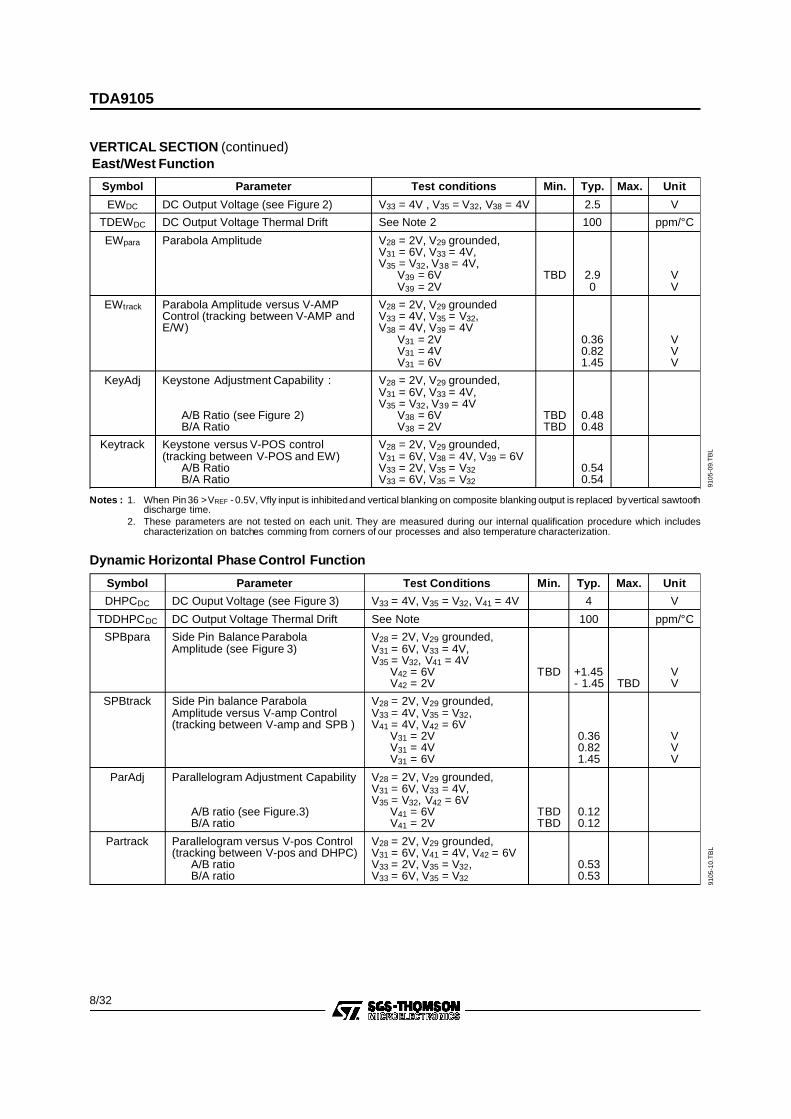
VERTICAL SECTION (continued)East/West Function
Symbol Parameter Test conditions Min. Typ. Max. Unit
EWDC DC Output Voltage (see Figure 2) V33 = 4V , V35 = V32, V38 = 4V 2.5 V
TDEWDC DC Output Voltage Thermal Drift See Note 2 100 ppm/°C
EWpara Parabola Amplitude V28 = 2V, V29 grounded,V31 = 6V, V33 = 4V,V35 = V32, V38 = 4V,
V39 = 6VV39 = 2V
TBD 2.90
VV
EWtrack Parabola Amplitude versus V-AMPControl (tracking between V-AMP andE/W)
V28 = 2V, V29 groundedV33 = 4V, V35 = V32,V38 = 4V, V39 = 4V
V31 = 2VV31 = 4VV31 = 6V
0.360.821.45
VVV
KeyAdj Keystone Adjustment Capability :
A/B Ratio (see Figure 2)B/A Ratio
V28 = 2V, V29 grounded,V31 = 6V, V33 = 4V,V35 = V32, V39 = 4V
V38 = 6VV38 = 2V
TBDTBD
0.480.48
Keytrack Keystone versus V-POS control(tracking between V-POS and EW)
A/B RatioB/A Ratio
V28 = 2V, V29 grounded,V31 = 6V, V38 = 4V, V39 = 6VV33 = 2V, V35 = V32V33 = 6V, V35 = V32
0.540.54
Notes : 1. When Pin 36 >VREF - 0.5V, Vfly input is inhibitedand vertical blanking on composite blanking output is replaced byvertical sawtoothdischarge time.
2. These parameters are not tested on each unit. They are measured during our internal qualification procedure which includescharacterization on batches comming from corners of our processes and also temperature characterization.
9105
-09.
TB
L
Dynamic Horizontal Phase Control Function
Symbol Parameter Test Conditions Min. Typ. Max. Unit
DHPCDC DC Ouput Voltage (see Figure 3) V33 = 4V, V35 = V32, V41 = 4V 4 V
TDDHPCDC DC Output Voltage Thermal Drift See Note 100 ppm/°C
SPBpara Side Pin Balance ParabolaAmplitude (see Figure 3)
V28 = 2V, V29 grounded,V31 = 6V, V33 = 4V,V35 = V32, V41 = 4V
V42 = 6VV42 = 2V
TBD +1.45- 1.45 TBD
VV
SPBtrack Side Pin balance ParabolaAmplitude versus V-amp Control(tracking between V-amp and SPB )
V28 = 2V, V29 grounded,V33 = 4V, V35 = V32,V41 = 4V, V42 = 6V
V31 = 2VV31 = 4VV31 = 6V
0.360.821.45
VVV
ParAdj Parallelogram Adjustment Capability
A/B ratio (see Figure.3)B/A ratio
V28 = 2V, V29 grounded,V31 = 6V, V33 = 4V,V35 = V32, V42 = 6V
V41 = 6VV41 = 2V
TBDTBD
0.120.12
Partrack Parallelogram versus V-pos Control(tracking between V-pos and DHPC)
A/B ratioB/A ratio
V28 = 2V, V29 grounded,V31 = 6V, V41 = 4V, V42 = 6VV33 = 2V, V35 = V32,V33 = 6V, V35 = V32
0.530.53
9105
-10.
TB
L
TDA9105
8/32
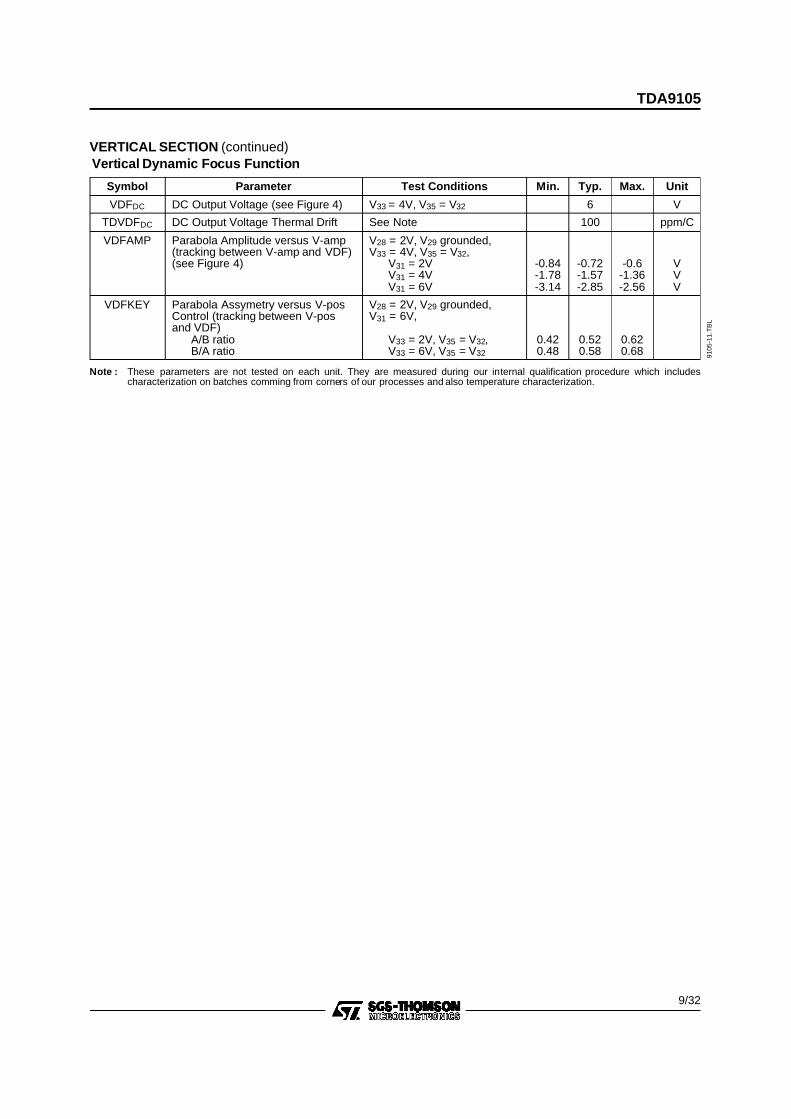
VERTICAL SECTION (continued)Vertical Dynamic Focus Function
Symbol Parameter Test Conditions Min. Typ. Max. Unit
VDFDC DC Output Voltage (see Figure 4) V33 = 4V, V35 = V32 6 V
TDVDFDC DC Output Voltage Thermal Drift See Note 100 ppm/C
VDFAMP Parabola Amplitude versus V-amp(tracking between V-amp and VDF)(see Figure 4)
V28 = 2V, V29 grounded,V33 = 4V, V35 = V32,
V31 = 2VV31 = 4VV31 = 6V
-0.84-1.78-3.14
-0.72-1.57-2.85
-0.6-1.36-2.56
VVV
VDFKEY Parabola Assymetry versus V-posControl (tracking between V-posand VDF)
A/B ratioB/A ratio
V28 = 2V, V29 grounded,V31 = 6V,
V33 = 2V, V35 = V32,V33 = 6V, V35 = V32
0.420.48
0.520.58
0.620.68
Note : These parameters are not tested on each unit. They are measured during our internal qualification procedure which includescharacterization on batches comming from corners of our processes and also temperature characterization.
9105
-11.
TB
L
TDA9105
9/32

1µF
22nF
47nF
10kΩ
1512
PH
AS
EF
RE
QU
EN
CY
CO
MP
VC
O
1011
89
PH
AS
EC
OM
P53
PH
AS
ES
HIF
TE
R
LOC
KU
NLO
CK
IDE
NT
2
PU
LSE
SH
AP
ER
416
SA
FE
TY
PR
OC
ES
SO
RV
S
21
23
PU
LSE
SH
AP
ER
PO
LD
ET
EC
T
17 147 6
V-R
EF
PLL
1IN
HIB
13
SC
OR
R
PU
LSE
SH
AP
ER
PO
LD
ET
EC
T
3426
29
24
V-R
EF VE
RT
OS
CR
AM
PG
EN
ER
AT
OR
2725
3130
3332
V-M
ID
40 424137 3938
X2
1
35
BLK
GE
N
3622
H-F
LY
V-S
YN
C
19
18T
DA
9105
VID
EO
UN
LOC
K
2.2 µ
F
220n
F
2.2 µ
F
1kΩ
6.49kΩ0.1%
47nF
680pF1%
1.8kΩ4.7µF
10nF
10kΩ
10kΩ
10k Ω
10kΩ
2.2µF
470n
F1%
150n
F1%
VC
C12
V
100nF
VC
CV
CC
VC
C
28
20
HO
UT
PU
TB
UF
FE
RM
OIR
E
10kΩ
H-S
ync
V-S
ync
VC
C
9105
-03.
EP
S
Figure 1 : Testing Circuit
TDA9105
10/32

EWDC
A
BEWPARA
9105
-04.
EP
S
Figure 2 : E/W Output
DHPCDC
A
B
SPBPARA
V41 = 6V
V42 = 6V
V42 = 2V
9105
-05.
EP
S
Figure 3 : Dynamic Horizontal Phase ControlOutput
VDFDC
A
BVDFAMP
V33 = 2V
9105
-06.
EP
S
Figure 4 : Vertical Dynamic Focus Function
TDA9105
11/32

TYPICAL VERTICAL OUTPUT WAVEFORMS
Function ControlPin
OutputPin
ControlVoltage Specification Picture Image
Vertical Size 31 30
2V
6V
VerticalPosition
DCControl
33 322V4V6V
3.2V3.5V3.8V
VerticalDC
In/Out35
13740
This terminal is a P incontrolling the center positionof geomet ric cor rec t ionsignals. When connected toPin 32, ”Autotracking” occurs.
VerticalS
Linearity25 30
2V
6V
VerticalC
Linearity29 30
2V
6V
9105
-13.
TB
L/9
105-
07.E
PS
TO
9105
-13.
EP
S
2V
4V
VPP
∆V
∆VVPP
= 4%
VPP
∆V
∆VVPP
= 5%
∆V
VPP∆VVPP
= 5%
TDA9105
12/32

TYPICAL GEOMETRY OUTPUT WAVEFORMS
Function ControlPin
OutputPin
ControlVoltage Specification Picture Image
TrapezoidControl 38 37
V39 = 4V
2V
6V
Pin CushionControl 39 37
V38 = 4V
2V
6V
ParrallelogramControl 41 40
V42 = 4V
2V
6V
Side PinBalanceControl
42 40
V41 = 4V
2V
6V
VerticalDynamic
Focus1
Note : The specification of Output voltage is indicated on 4VPP vertical sawtooth output condition.The output voltage depends on verticalsawtooth output voltage.
9105
-14.
TB
L/9
105-
14.E
PS
TO
9105
-22.
EP
S
4.95V
2.95V
2.5V4.95V
2.95V
2.5V
0V
2.9V
2.5V
3V4V
3V4V
1.45V
1.45V
4V
3V
6V
TDA9105
13/32

OPERATING DESCRIPTIONGENERAL CONSIDERATIONSPower Supply
The typical value of the power supply voltage VCCis 12V. Perfect operation is obtained if VCC is main-tained in the limits : 10.8V → 13.2V.In order to avoid erratic operation of the circuitduring the transient phase of VCC switching on, orswitching off, the value of VCC ismonitored and theoutputs of the circuit are inhibited if VCC < 7.6 typi-cally.In order tohave a very good powersupplyrejection,the circuit is internally powered by several internalvoltage references (The unique typical value ofwhich is 8V). Two of these voltage references areexternally accessible, one for the vertical part andone for the horizontal part. These voltage refer-ences can be used for the DC control voltagesapplied on the concerned pins by the way of poten-tiometers or digital to analog converters (DAC’s).Furthermore it isnecessary to filter the a.m. voltagereferences by the use of external capacitor con-nected to ground, in order to minimize the noiseand consequently the ”jitter” on vertical and hori-zontal output signals.
DC Control AdjustmentsThe circuit has 10 adjustmentcapabilities : 2 for thehorizontal part, 2 for the E/W correction, 4 for thevertical part, 2 for the Dynamic Horizontal phasecontrol.The corresponding inputs of the circuit has to bedriven with a DC voltage typically comprised be-tween 2 and 6V for a value of the internal voltagereference of 8V.
PWMDAC
Output
DC ControlVoltage
VREF
9105
-23.
EP
S
Figure 5 : Example of Practical DC ControlVoltage Generation
9105
-25.
EP
S
Figure 7
H-SYNC 1.6V
9105
-24.
EP
S
Figure 6 : Input Structure
In order to have a good tracking with the voltagereference value, it’s better to maintain the controlvoltages between VREF/4 and 3/4 ⋅ VREF.The input current of the DC control inputs is typi-cally very low (about a few µA). Depending on theinternal structure of the inputs, it can be positive ornegative (sink or source).
HORIZONTAL PARTInput section
The horizontal input is designed to be sensitive toTTL signals typically comprised between 0 and 5V.The typical threshold of this input is 1.6V. This inputstage uses an NPN differential stage and the inputcurrent is very low.
Concerning the duty cycle of the input signal, thefollowing signals may be applied to the circuit.Using internal integration, both signals are recog-nized on condition that Z/T ≤ 25%. Synchronisationoccurs on the leading edge of the internal syncsignal. The minimum value of Z is 0.7µs.
PLL1The PLL1 is composed of a phase comparator, anexternal filter and a Voltage Controlled Oscillator(VCO).The phase comparator is a ”phase frequency” type,designed in CMOS technology. This kind of phasedetector avoids locking on false frequencies. It isfollowed by a ”charge pump”, composed of 2 cur-rent sources sink and source (I = 1mA typ.)
TDA9105
14/32

OPERATING DESCRIPTION (continued)
LOCKDET
2
H-LOCKOUT
13
H-LOCKCAP
COMP1INPUTINTERFACE17H-SYNC
High
CHARGEPUMP
Low
PLLINHIBITION
VCO
14
PLL1INHIB
12 11 10
PLL1F R0 C0
PHASEADJUST
E2
15
H-POS
3.2V
OSC
9105
-26.
EP
S
Figure 8 : Principle Diagram
The dynamic behaviour of the PLL is fixed by anexternal filter which integrates the current of thecharge pump. A ”CRC” filter is generally used (seeFigure 9).PLL1 is inhibited by applying a high level on Pin 14(PLLinhib)which is a TTLcompatible input.The inhibi-tion results from the opening of a switch located be-tween the charge pump and the filter (see Figure 8).The VCO uses an external RC network. It deliversa linear sawtooth obtained by charge and dis-charge of the capacitor, by a current proportionnalto the current in the resistor. typical thresholds ofsawtooth are 1.6V and 6.4V (see Figure 10).The control voltage of the VCO is typically com-prised between 1.6V and 6V (see Figure 10). Thetheoreticalfrequencyrangeof this VCOis in theratio1 → 3.75, but due to spread and thermal drift ofexternalcomponents and the circuit itself, the effec-
12
PLL1F
9105
-27.
EP
S
Figure 9
tive frequency range has to be smaller (e.g. 30kHz→ 85kHz). In the absence of synchronisationsignalthe control voltage is equal to 1.6V typ. and theVCOoscillates on its lowest frequency (free frequency).The synchro frequencyhas to bealwayshigher thanthe free frequency anda margin has to be taken. Asan example for a synchro range from 30kHz to85kHz, the suggested free frequency is 27kHz.
11
12LoopFilter
R0
1.6V
6.4V
10
C0
6.4V
1.6V0 0.75T T
RSFLIP FLOP
(1.6V < V < 6V)12
I0
I0
2
4 I0
2
9105
-28.
EP
S
Figure 10 : Details of VCO
TDA9105
15/32
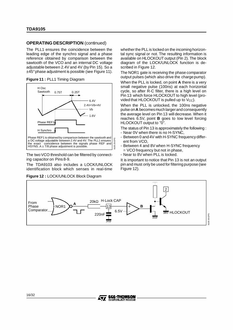
OPERATING DESCRIPTION (continued)The PLL1 ensures the coincidence between theleading edge of the synchro signal and a phasereference obtained by comparison between thesawtooth of the VCO and an internal DC voltageadjustable between 2.4V and 4V (by Pin 15). So a±45°phase adjustment is possible (see Figure 11).
20kΩ
220nF
13FromPhaseComparator
NOR1A
6.5VB
H-Lock CAP
2
HLOCKOUT91
05-3
0.E
PS
Figure 12 : LOCK/UNLOCK Block Diagram
H OscSawtooth
Phase REF1
H Synchro
1.6V
Vb
6.4V
2.4V<Vb<4V
0.75T 0.25T
Phase REF1 is obtained by comparison between the sawtooth anda DC voltage adjustable between 2.4V and 4V. The PLL1 ensuresthe exact coincidence between the signals phase REF andHSYNS. A ± T/8 phase adjustment is possible.
9105
-29.
EP
S
Figure 11 : PLL1 Timing Diagram
The two VCO threshold can be filtered by connect-ing capacitor on Pins 8-9.The TDA9103 also includes a LOCK/UNLOCKidentification block which senses in real-time
whether the PLL is locked on the incoming horizon-tal sync signal or not. The resulting information isavailable on HLOCKOUT output (Pin 2). The blockdiagram of the LOCK/UNLOCK function is de-scribed in Figure 12.The NOR1 gate is receiving the phase comparatoroutput pulses (which also drive the chargepump).When the PLL is locked, on point A there is a verysmall negative pulse (100ns) at each horizontalcycle, so after R-C filter, there is a high level onPin 13 which force HLOCKOUT to high level (pro-vided that HLOCKOUT is pulled up to VCC).When the PLL is unlocked, the 100ns negativepulse onA becomesmuch largerand consequentlythe average level on Pin 13 will decrease. When itreaches 6.5V, point B goes to low level forcingHLOCKOUT output to ”0”.The status of Pin 13 is approximately the following :- Near 0V when there is no H-SYNC,- Between 0 and 4V with H-SYNC frequency differ-
ent from VCO,- Between 4 and 8V when H-SYNC frequency
= VCO frequency but not in phase,- Near to 8V when PLL is locked.It is important to notice that Pin 13 is not an outputpin and must only be used for filtering purpose (seeFigure 12).
TDA9105
16/32

H OscSawtooth
H Drive
1.6V
4V
6.4V
0.75T 0.25T
Ts
Duty Cycle
InternallyShaped Flyback
Flyback
9105
-31.
EP
S
The duty cycle of H-drive is adjustable between 30% and 50%.
Figure 13 : PLL2 Timing Diagram
20kΩ
Q1
GND 0V
5HFLY
400Ω
9105
-32.
EP
S
Figure 14 : Flyback Input Electrical Diagram
OPERATING DESCRIPTION (continued)PLL2 The PLL2 ensures a constant position of the
shaped flyback signal in comparison with the saw-tooth of the VCO (see Figure 13).The phase comparator of PLL2 is followed by acharge pump with a ±0.5mA (typ.) output current.The flyback input iscomposedofan NPNtransistor.This input has to be current driven.The maximum recommanded input current is 2mA(see Figures 14 and 15).
C Lockdet
LOCKDET
COMP1INPUTINTERFACE
CHARGEPUMP
PLLINHIBITION
VCO
PHASEADJUST
PLL1INHIB
HorizontalAdjust
R0 C0Filter
High
LowE2
3.2V
OSC
COMP2CHARGEPUMP
High
Low
RAPCYC
EN
AdjustRapcyc
CapPHi2
PWM LOGIPWM BUFFER
FLYBACK
SortCOLL
Flyback
SortEM
VBVA
HorizontalInput
13 14 12 11 10
17
4 3
15
5
21
20
HLOCKOUT2
4V
9105
-33.
AI
Figure 15 : Dual PLL Block Diagram
TDA9105
17/32

20
21
H-DRIVE
VCC
20
21
H-DRIVE
VCC
9105
-34.
EP
S
Figure 16 : Output stage simplified diagram,showing the two possibilities ofconnection
OPERATING DESCRIPTION (continued)Output SectionThe H-drive signal is transmitted to the outputthrough a shaping block ensuring a duty cycleadjustable from 30% to 50%. In order to ensure areliable operation of the scanning power part, theoutput is inhibited in the following circumstances :- VCC too low,- Xray protection activated,- During the horizontal flyback,- Output voluntarily inhibited through Pin 4.The outputstage is composed of a Darlington NPNbipolar transistor. Both the collector and the emitterare accessible (see Figure 16).The outputDarlington is in off-state when thepowerscanning transistor is also in off-state.The maximum output current is 20mA, and thecorrespondingvoltage dropof the outputdarlingtonis 1.1V typically.It is evident that the power scanning transistorcannot be directly driven by the integrated circuit.An interface has to be designed betweenthe circuitand the power transistor which can be of bipolar orMOS type.
Outputs inhibitionThe application of a voltage lower than 1V (typ.) onPin 4 (duty cycle adjust) inhibits the horizontal andvertical outputs. This is not memorised.
LOGICBLOCK
V-fly
Vsync
V sawtoothretrace time
H-fly to 2ND PLL
H OUTPUTINHIBITION
V OUTPUTINHIBITION
COMPOSITEBLANKING
SR
Q
H-Duty cycle
1V
Flyback
0.7V
XRAY
REF
VCC
VCC off
XRAY Protection
Inhibition
VCC
Checking
9105
-35.
EP
S
Figure 17 : Safety Functions Block Diagram
X-RAY PROTECTION : the activation of the X-rayprotection is obtained by application of a high levelon the X-ray input (>8V). Consequences of X-rayprotection are :- Inhibition of H drive output,- Activation of composite blanking output.The reset of this protection is obtained by VCCswitch off (see Figure 17).
TDA9105
18/32

OPERATING DESCRIPTION (continued)Moire Function
23Ck
D
Q
QRst
H-SYNC
Ck
D
Q
Q
Monosta ble
V-SYNC
9105
-36.
EP
S
Figure 18 : Moire Function Block Diagram
H
V
MOIRE
H
V
MOIRE
ODD FRAME
EVEN FRAME
9105
-37.
EP
S
Figure 19 : Moire Output Waveform
Geometric Corrections
The principle is represented in Figure 20.Starting from the vertical ramp, a parabola shapedis generatedfor E/Wcorrection,dynamic horizontalphase control correction, and vertical dynamic Fo-cus correction.The core of the parabola generator is an analogmultiplier. The output current of which is equal to :
∆I = k (VRAMP - VDCIN)2.
Where VRAMP is the vertical ramp, typically com-prised between 2 and 5V, VDCIN is a vertical DCinput adjustable in the range 3.2V → 3.8V in orderto generate a dissymmetric parabola if required(keystone adjustment).In order to keep good screen geometry for any enduser preferencesadjustment we implemented the
possibility to have ”geometry tracking ”. To enablethe ”tracking” function, the VDCOUT must be con-nected to VDCIN.
It is possible to inhibit VPOS tracking by applying afixed DC voltage on the VDCIN Pin.
This DC voltage in that case must be taken fromthe vertical reference and adjusted to 3.5V with anexternal bridge resistor.
Due to large output stages voltage range (E/W,BALANCE, FOCUS), the combination of trackingfunction with maximum vertical amplitude max. ormin. vertical position and maximum gain on the DCcontrol inputs may leads to the output stages satu-ration. This must be avoided by limiting the outputvoltage by apropriateDC control voltages.
TDA9105
19/32

OPERATING DESCRIPTION (continued)Geometric Corrections (continued)
SIDE PIN BAL. OUT
EW OUT
VERT. DYN. FOCUS OUT
VDCIN
KEYSTONE
EW AMP
VDCIN
KEY BALANCE
SIDEPIN AMP
2
VDCIN
ANALOG MULTIPLIER
VERTICAL RAMP
9105
-38.
EP
S
Figure 20 : Geometric Corrections Principle
For E/Wpart andDynamicHorizontal phasecontrolpart, a sawtooth shaped differential current in thefollowingform isgenerated: ∆I’ = k’ (VRAMP -VDCIN).Then ∆I and ∆I’ are added together and convertedinto voltage.
These two parabola are respectively available onPin 37 and Pin 40 by the way of an emitter followerwhich has to be biased by an external resistor(10kΩ). They can be DC coupled with externalcircuitry.EW VOUT = 2.5V + K1’ (VRAMP - VDCIN)
+ K1 (VRAMP - VDCIN)2
K1 is adjustable by EW amp control (Pin 39)K1’ is adjustable by KEYST control (Pin 38)
Dyn. Hor.Phase Control
VOUT = 4V + K2’ (VRAMP - VDCIN)+ K2 (VRAMP - VDCIN)2
K2 is adjustable by SPB amp control (Pin 42)K2’ is adjustable by KEYBAL control (Pin 41)
For vertical dynamic focus part, only a constantamplitude parabola is generated in the form :
VOUT = 6V - 0.75 x (VAMP - VDCIN)2.
The outputconnection is the same as the two othercorrections (Pins 37-40).
It is important to note that the parasitic paraboladuring the discharge of the vertical oscillator ca-pacitor is suppressed.
TDA9105
20/32

OPERATING DESCRIPTION (continued)VERTICAL PART
27
28
29
37
38
31
25
39
PARABOLAGENERATOR
SYNCHRO OSCILLATOR34
OSCCAPDISCH.
V_SYNC
POLARITY
SAMPLING SAMP.CAP
Vlow Sawth.
Disch.
REF
TRANSCONDUCTANCEAMPLIFIERCHARGE CURRENT
30 VERT_OUT
VERT_AMP
VS_AMP
COR_C
S CORRECTION
C CORRECTION
EW_AMP
EW_OUT
EW_CENT
SPB_AMP
SPB_OUT
SPB_CENT
V_FOCUS1
41 42
40
9105
-39.
EP
S
Figure 21 : Vertical Part Block Diagram
The vertical part generates a fixed amplitude rampwhich can be affected by a S and C correctionshape. Then, the amplitude of this ramp is adjustedto drive an external power stage.
The internal reference voltage used for the verticalpart is available between Pin 26 and Pin 24. It canbe usedas voltage reference forany DC adjusment
to keep a high accuracy to each adjustment. Itstypical value is :
V26 = VREF = 8V.
The charge of the external capacitor on Pin 27(VCAP) generates a fixed amplitude ramp betweenthe internal voltages, VL (VL = VREF/4) and VH(VH = 5/8 ⋅ VREF).
TDA9105
21/32

OPERATING DESCRIPTION (continued)VERTICAL PART (continued)
FunctionWhen the synchronisation pulse is not present, aninternal current source sets the free running fre-quency. For an external capacitor, COSC = 150nF,the typical free running frequency is 100Hz.Typical free running frequency can be calculatedby :
f0 (Hz) = 1.5 ⋅ 10−5 ⋅1
COSC (nF)A negative or positive TTL level pulse applied onPin 34 (VSYNC) can synchronise the ramp in thefrequencyrange [fmin, fmax]. This frequency rangedepends on the external capacitor connected onPin 27. A capacitor in the range [150nF, 220nF] isrecommanded for application in the followingrange : 50Hz to 120Hz.Typical maximum and minimum frequency, at 25°Cand without any correction (S correction or C cor-rection), can be calculated by :fmax = 2.5 ⋅ f0 and fmin = 0.33 ⋅ f0If S or C corrections are applied, these values areslighty affected.If an external synchronisation pulse is applied, theinternal oscillator is automaticaly caught but theamplitude is no more constant. An internal correc-tion is activated to adjust it in less than half asecond: the highest voltage of the ramp on Pin 27is sampledon the sampling capacitorconnectedonPin 25 (VAGCCAP) at each clock pulse and atransconductance amplifier generates the chargecurrent of the capacitor. The ramp amplitude be-comes again constant.It is recommanded to usea AGC capacitor with lowleakage current. A value lower than 100nA is man-datory.Pin 36, Vfly is the vertical flyback input used togenerate the composite blanking signal. If Vfly isnot used, (VREF - 0.5), at minimum, must be con-nected to this input.
DC Control AdjustmentsThen, S and C correction shapes can be added tothis ramp. This frequency independent S and Ccorrections are generated internally; their ampli-
tude are DC adjustable on Pin 28 (VSAMP) andPin 29 (COR-C).S correction is non effective for VSAMP lower thanVREF/4 and maximum for VSAMP = 3/4 ⋅ VREF.C correction is non effective for COR-C groundedand maximum for :COR-C = VREF/4 or COR-C = 3/4 ⋅ VREF.Endly, the amplitude of this S and C corrected rampcan be adjusted by the voltage applied on Pin 31(VAMP). The adjusted ramp is available on Pin 30(VOUT) to drive an external power stage. The gainof thisstage is typically±30% when voltage appliedon Pin 31 is in the range VREF/4 to 3/4 ⋅ VREF. TheDC value of this ramp is kept constant in thefrequency range , for any correction applied on it.Its typical value is : VDCOUT = VMID = 7/16 ⋅ VREF.A DC voltage is available on Pin 32 (VDCOUT). It isdriven by the voltage applied on Pin 33 (VPOS)For a voltage control range between VREF/4 and3/4 ⋅ VREF, the voltage available on Pin 32 is :VDCOUT = 7/16 ⋅ VREF ± 300mV.So, the VDCOUT voltage is correlated with DC valueof VOUT. It increases the accuracy when tempera-ture varies.
Basic EquationsIn first approximation, the amplitude of the ramp onPin 30 (VOUT) is :
VOUT - VMID = (VCAP - VMID) [1 + 0.16 ⋅ (VAMP - VREF/2)]
with VMID = 7/16 ⋅ VREF ; typically 3.5VVMID is the middle value of the ramp on Pin 27VCAP = V27 , ramp with fixed amplitude.
On Pin 32 (VDCOUT), the voltage (in volts) is calcu-lated by : VDCOUT =VMID + 0.16 ⋅ (VPOS - VREF/2).VPOS is the voltage applied on Pin 33.The current available on Pin 27(when VSAMP = VREF/4) is :IOSC = 3/8 ⋅ VREF ⋅ COSC ⋅ fCOSC : capacitor connected on Pin 27f synchronisation frequencyThe recommanded capacitor value on Pin 25(VAGC) is 470nF. Its ensures a good stability of theinternal closed loop.
TDA9105
22/32

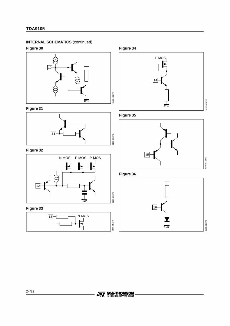
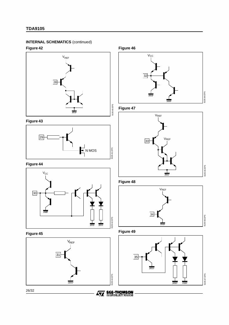
INTERNAL SCHEMATICS
1mA max
Href
Pins 1-37-40
9105
-40.
EP
S
Figure 22
N MOS
10mA max.
Pins2-22-23V CC
9105
-41.
EP
SFigure 23
3
Href
9105
-42.
EP
S
Figure 24
4
P MOS
9105
-43.
EP
S
Figure 25
5
9105
-44.
EP
S
Figure 26
7
VCC
9105
-45.
EP
S
Figure 27
8
9105
-46.
EP
S
Figure 28
9
9105
-47.
EP
S
Figure 29
TDA9105
23/32
INTERNAL SCHEMATICS (continued)
10
9105
-48.
EP
S
Figure 30
11
9105
-49.
EP
S
Figure 31
12
N MOS P MOS P MOS
9105
-50.
EP
S
Figure 32
13 N MOS
9105
-51.
EP
S
Figure 33
14
P MOS
9105
-52.
EP
S
Figure 34
15
9105
-53.
EP
S
Figure 35
1691
05-5
4.E
PS
Figure 36
TDA9105
24/32

17
P MOS
9105
-55.
EP
S
Figure 37
INTERNAL SCHEMATICS (continued)
20
21
20mA max.
9105
-56.
EP
SFigure 38
27
VREF VCC
VREF
VREF
N
P
N MOS
9105
-59.
EP
S
Figure 41
25N
P MOS
P
N
P
9105
-57.
EP
S
Figure 39
26
VCC
9105
-58.
EP
S
Figure 40
TDA9105
25/32
INTERNAL SCHEMATICS (continued)
28
VREF
9105
-60.
EP
S
Figure 42
29
N MOS
9105
-61.
EP
S
Figure 43
30
VCC
9105
-62.
EP
S
Figure 44
31
VREF
9105
-63.
EP
S
Figure 45
32
VCC
9105
-64.
EP
S
Figure 46
33
VREF
VREF
9105
-65.
EP
S
Figure 47
34
VREF
9105
-66.
EP
S
Figure 48
35
9105
-67.
EP
S
Figure 49
TDA9105
26/32

INTERNAL SCHEMATICS (continued)
36
VREF
P MOS
9105
-68.
EP
S
Figure 50
Pins38-3941-42
VREF
9105
-69.
EP
S
Figure 51
TDA9105
27/32

+
IC1
+ +
+
+
VR
EF
off
on
S1
+
+
J18
+
HF
LYJ1b
HO
UT
+12
V
+
1H
FLY
TP
2X
RA
YIN
J2H
SY
NC
TP
3
J5V
SY
NC
TP
7
TP
6B
LK
J19
1
TP
5T
P4
J3 1
+12
V
+
HD
RIV
E
J22
T1
G55
76-0
0
+
R44
10Ω
HO
RIZ
ON
TA
LD
RIV
ER
ST
AG
E
1J23
VY
OK
E
1-1
2VJ2
1
R36
12kΩ
R70
12kΩ
-12V
+
R38
5.6k
Ω
+12
V
+
172
63 5
4
VE
RT
ICA
LD
EF
LEC
TIO
NS
TA
GE
J24
E/W
+12
V
E/W
PO
WE
RS
TA
GE
+
1 2 3 4 5 6 7 8 9 10 16 17 18 19 20
26272829303637383940
11 12 13 14 15 2122232425313233343542 41
T D A 9 1 0 5
2 3 1 2 3
12
34
BC
557
Q3
Q4
BC
557
Q9
TIP
122
C10
100n
F
C11
470p
FC
1447
0µF
C31
100n
F
C15
220n
F
C32
100n
F
C12
100µ
F35
V
C13
470µ
F
Q10
BC
547
Q1
BC
557
Q2
ST
D5N
20
C20
100µ
F
C19
1nF
R35
1kΩ
R45
22kΩ
R46
560Ω
R47
a47
Ω3W
R37
5.6k
Ω
D1
1N40
04
R41
1.5Ω
R39
220Ω
1/2W
R40
1Ω
1/2W
R92
1kΩ
R52
27kΩ R51
6.2k
ΩR
5447
0Ω
C44
220p
F
R57
270k
Ω
R59
2.2Ω
1W
R53
1kΩ
R55
270k
Ω
R56 39
kΩ
C9
100n
FC
810
0µF
R33
10kΩ
C28
47µF
TP
1 C5
150n
F
470n
F
C42
1µF
C43
1µF
C27
100n
F
C4
C40
1µF
C41
1µF
C6
220n
F
C7
4.7µ
FR
311.
8kΩ
R32
680p
F5%C50
C3
10nF
C45
220p
F
C34
1µF
C36
1µF
C30
C29
100n
F47
µF
R71
10kΩ
R7410kΩ
R7310kΩ
R47
b33
Ω3W
+C
531µ
F+12
V L1 10µH
TP
11
TP
15R
8515
kΩ
R86
4.7k
Ω
1
R81
43.2
kΩ
R82
33.2
kΩ
1% 1%
VR
EF
+C37
1µF
KE
YS
TV
SH
IFT
CC
OR
VS
IZE
PIN
CS
HS
CO
RH
SIZ
E
J3b
HR
EF
VR
EF
HD
FH
SH
IFT
KE
YB
AL
SB
PA
MP
J2b
0/5V
to2/
6VIN
TE
RF
AC
E
12
34
12
34
56
7
R2120kΩ
R5120kΩ
R8120kΩ
R310kΩ
R610kΩ
R910kΩ
R1210kΩ
R1510kΩ
R1810kΩ
R2110kΩ
R2410kΩ
R2710kΩ
R3010kΩ
R11120kΩ
R14120kΩ
R17120kΩ
R20120kΩ
R23120kΩ
R26120kΩ
R29120kΩ
R223.9kΩ
R193.9kΩ
R253.9kΩ
R283.9kΩ
R163.9kΩ
R133.9kΩ
R103.9kΩ
R73.9kΩ
R43.9kΩ
R13.9kΩ
R75
27kΩ
+C38
1µF
C1
22nF
SW
1
R84
47kΩ
R87
10kΩ
HR
EF
TP
12
R91
J25
1D
YN
FO
CU
S CO
N1
R88
10kΩ
+12
V
TP
13
++
C35
C39
1µF
1µF
C52
C2
TP
14
R90
1Ω
C51
D4
1N41
48
R80
2.7k
Ω
C48
1nF
63V
IC2
TD
A81
72
D5
1N41
48
5.6k
Ω
47nF
47nF
R83
1kΩ
R93
R94
15kΩ
330k
Ω
C54
15nF
R89
4.7k
Ω 6.49
kΩ1%
9105
-70.
EP
S
Figure 52 : Demonstration Board
APPLICATION DIAGRAMS
TDA9105
28/32

Pc847kΩ
Pc747kΩ
Pc647kΩ
Pc547kΩ
Pc447kΩ
Pc947kΩ
Pc1047kΩ
Pc1147kΩ
Pc1247kΩ
Pc134.7kΩ
Pc347kΩ
1
+5V
Cc4
10µF
Jc4 1
Jc26
CO
N1
12
34SB
PA
MP
KE
YB
AL
HF
LY
HS
HIF
T
HO
UT
HD
F
CC
OR
PIN
CS
H
SC
OR
VS
IZE
HS
IZE
VS
HIF
T
KE
YS
T
12
34
12
34
56
7
Cc4
10µF
Cc5
100n
F
+12
V
TT
Cc1
47pF
+12
VC X
R C
Jc1
Q
R
+12
VP
c247
kΩC
c247
pFR
CC
X T T
Q Q
Icc1
B14
528
Icc1
A14
528
Jc2
Jc3
Pc147kΩ
Q
9105
-71.
EP
S
Figure 53 : Control Board
APPLICATION DIAGRAMS
TDA9105
29/32

9105
-72.
TIF
Figure 54 : PCB Layout
APPLICATION DIAGRAMS
TDA9105
30/32

9105
-73.
EP
S
Figure 55 : ComponentsLayout
APPLICATION DIAGRAMS
TDA9105
31/32

A1
B eB1
D
22
21
42
1
LA
e1
A2
c
E1
E
e2
Gage Plane
.015
0,38
e2
e3
E
SDIP42
PM
SD
IP42
.EP
S
PACKAGE MECHANICAL DATA42 PINS - PLASTIC SHRINK DIP
DimensionsMillimeters Inches
Min. Typ. Max. Min. Typ. Max.A 5.08 0.200
A1 0.51 0.020A2 3.05 3.81 4.57 0.120 0.150 0.180B 0.36 0.46 0.56 0.0142 0.0181 0.0220
B1 0.76 1.02 1.14 0.030 0.040 0.045c 0.23 0.25 0.38 0.0090 0.0098 0.0150
D 37.85 38.10 38.35 1.490 1.5 1.510E 15.24 16.00 0.60 0.629E1 12.70 13.72 14.48 0.50 0.540 0.570
e 1.778 0.070e1 15.24 0.60
e2 18.54 0.730e3 1.52 0.060L 2.54 3.30 3.56 0.10 0.130 0.140
SD
IP42
.TB
L
Information furnished is believed to be accurate and reliable. However, SGS-THOMSON Microelectronics assumes no responsibilityfor the consequences of use of such information nor for any infringement of patents or other rights of third parties which may resultfrom its use. No licence is granted by implication or otherwise under any patent or patent rights of SGS-THOMSON Microelectronics.Specifications mentioned in this publication are subject to change without notice. This publication supersedes and replaces allinformation previously supplied. SGS-THOMSON Microelectronics products are not authorized for use as critical components in lifesupport devices or systems without express written approval of SGS-THOMSON Microelectronics.
1996 SGS-THOMSON Microelectronics - All Rights Reserved
Purchase of I 2C Components of SGS-THOMSON Microelectronics, conveys a license under the PhilipsI2C Patent. Rights to use these components in a I 2C system, is granted provided that the system conforms to
the I2C Standard Specifications as defined by Philips.
SGS-THOMSON Microelectronics GROUP OF COMPANIESAustralia - Brazil -Canada - China - France - Germany - Hong Kong - Italy - Japan - Korea - Malaysia - Malta - Morocco
The Netherlands - Singapore - Spain - Sweden - Switzerland - Taiwan - Thailand - United Kingdom - U.S.A.
TDA9105
32/32

This datasheet has been download from:
www.datasheetcatalog.com
Datasheets for electronics components.
Related Documents