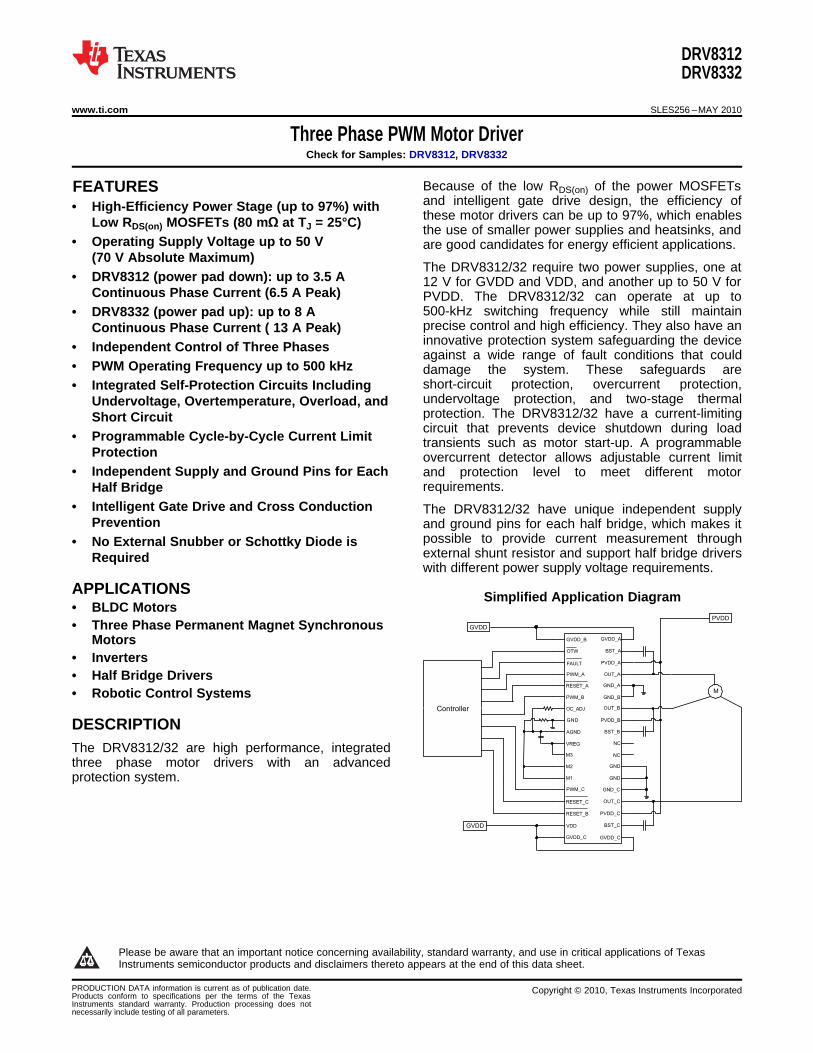
GVDD GVDD PVDD M Controller RESET_A PWM_B OC_ADJ GND GND_A GND_B OUT_B PVDD_B AGND VREG M3 M2 BST_B NC NC GND RESET_C RESET_B VDD GVDD_C OUT_C PVDD_C BST_C GVDD_C PWM_C GND_C M1 GND GVDD_B OTW FAULT PWM_A GVDD_A BST_A PVDD_A OUT_A DRV8312 DRV8332 www.ti.com SLES256 – MAY 2010 Three Phase PWM Motor Driver Check for Samples: DRV8312, DRV8332 Because of the low R DS(on) of the power MOSFETs 1FEATURES and intelligent gate drive design, the efficiency of • High-Efficiency Power Stage (up to 97%) with these motor drivers can be up to 97%, which enables Low R DS(on) MOSFETs (80 mΩ at T J = 25°C) the use of smaller power supplies and heatsinks, and • Operating Supply Voltage up to 50 V are good candidates for energy efficient applications. (70 V Absolute Maximum) The DRV8312/32 require two power supplies, one at • DRV8312 (power pad down): up to 3.5 A 12 V for GVDD and VDD, and another up to 50 V for Continuous Phase Current (6.5 A Peak) PVDD. The DRV8312/32 can operate at up to 500-kHz switching frequency while still maintain • DRV8332 (power pad up): up to 8 A precise control and high efficiency. They also have an Continuous Phase Current ( 13 A Peak) innovative protection system safeguarding the device • Independent Control of Three Phases against a wide range of fault conditions that could • PWM Operating Frequency up to 500 kHz damage the system. These safeguards are short-circuit protection, overcurrent protection, • Integrated Self-Protection Circuits Including undervoltage protection, and two-stage thermal Undervoltage, Overtemperature, Overload, and protection. The DRV8312/32 have a current-limiting Short Circuit circuit that prevents device shutdown during load • Programmable Cycle-by-Cycle Current Limit transients such as motor start-up. A programmable Protection overcurrent detector allows adjustable current limit • Independent Supply and Ground Pins for Each and protection level to meet different motor requirements. Half Bridge • Intelligent Gate Drive and Cross Conduction The DRV8312/32 have unique independent supply Prevention and ground pins for each half bridge, which makes it possible to provide current measurement through • No External Snubber or Schottky Diode is external shunt resistor and support half bridge drivers Required with different power supply voltage requirements. APPLICATIONS Simplified Application Diagram • BLDC Motors • Three Phase Permanent Magnet Synchronous Motors • Inverters • Half Bridge Drivers • Robotic Control Systems DESCRIPTION The DRV8312/32 are high performance, integrated three phase motor drivers with an advanced protection system. 1 Please be aware that an important notice concerning availability, standard warranty, and use in critical applications of Texas Instruments semiconductor products and disclaimers thereto appears at the end of this data sheet. PRODUCTION DATA information is current as of publication date. Copyright © 2010, Texas Instruments Incorporated Products conform to specifications per the terms of the Texas Instruments standard warranty. Production processing does not necessarily include testing of all parameters.

Welcome message from author
This document is posted to help you gain knowledge. Please leave a comment to let me know what you think about it! Share it to your friends and learn new things together.
Transcript
GVDD
GVDD
PVDD
M
Controller
RESET_A
PWM_B
OC_ADJ
GND
GND_A
GND_B
OUT_B
PVDD_B
AGND
VREG
M3
M2
BST_B
NC
NC
GND
RESET_C
RESET_B
VDD
GVDD_C
OUT_C
PVDD_C
BST_C
GVDD_C
PWM_C GND_C
M1 GND
GVDD_B
OTW
FAULT
PWM_A
GVDD_A
BST_A
PVDD_A
OUT_A
DRV8312DRV8332
www.ti.com SLES256 –MAY 2010
Three Phase PWM Motor DriverCheck for Samples: DRV8312, DRV8332
Because of the low RDS(on) of the power MOSFETs1FEATURES
and intelligent gate drive design, the efficiency of• High-Efficiency Power Stage (up to 97%) withthese motor drivers can be up to 97%, which enablesLow RDS(on) MOSFETs (80 mΩ at TJ = 25°C) the use of smaller power supplies and heatsinks, and
• Operating Supply Voltage up to 50 V are good candidates for energy efficient applications.(70 V Absolute Maximum)
The DRV8312/32 require two power supplies, one at• DRV8312 (power pad down): up to 3.5 A 12 V for GVDD and VDD, and another up to 50 V for
Continuous Phase Current (6.5 A Peak) PVDD. The DRV8312/32 can operate at up to500-kHz switching frequency while still maintain• DRV8332 (power pad up): up to 8 Aprecise control and high efficiency. They also have anContinuous Phase Current ( 13 A Peak)innovative protection system safeguarding the device• Independent Control of Three Phasesagainst a wide range of fault conditions that could
• PWM Operating Frequency up to 500 kHz damage the system. These safeguards areshort-circuit protection, overcurrent protection,• Integrated Self-Protection Circuits Includingundervoltage protection, and two-stage thermalUndervoltage, Overtemperature, Overload, andprotection. The DRV8312/32 have a current-limitingShort Circuitcircuit that prevents device shutdown during load
• Programmable Cycle-by-Cycle Current Limit transients such as motor start-up. A programmableProtection overcurrent detector allows adjustable current limit
• Independent Supply and Ground Pins for Each and protection level to meet different motorrequirements.Half Bridge
• Intelligent Gate Drive and Cross Conduction The DRV8312/32 have unique independent supplyPrevention and ground pins for each half bridge, which makes it
possible to provide current measurement through• No External Snubber or Schottky Diode isexternal shunt resistor and support half bridge driversRequiredwith different power supply voltage requirements.
APPLICATIONS Simplified Application Diagram• BLDC Motors• Three Phase Permanent Magnet Synchronous
Motors• Inverters• Half Bridge Drivers• Robotic Control Systems
DESCRIPTIONThe DRV8312/32 are high performance, integratedthree phase motor drivers with an advancedprotection system.
1
Please be aware that an important notice concerning availability, standard warranty, and use in critical applications of TexasInstruments semiconductor products and disclaimers thereto appears at the end of this data sheet.
PRODUCTION DATA information is current as of publication date. Copyright © 2010, Texas Instruments IncorporatedProducts conform to specifications per the terms of the TexasInstruments standard warranty. Production processing does notnecessarily include testing of all parameters.

DRV8312DRV8332
SLES256 –MAY 2010 www.ti.com
This integrated circuit can be damaged by ESD. Texas Instruments recommends that all integrated circuits be handled withappropriate precautions. Failure to observe proper handling and installation procedures can cause damage.
ESD damage can range from subtle performance degradation to complete device failure. Precision integrated circuits may be moresusceptible to damage because very small parametric changes could cause the device not to meet its published specifications.
ABSOLUTE MAXIMUM RATINGSOver operating free-air temperature range unless otherwise noted (1)
VALUE
VDD to GND –0.3 V to 13.2 V
GVDD_X to GND –0.3 V to 13.2 V
PVDD_X to GND_X (2) –0.3 V to 70 V
OUT_X to GND_X (2) –0.3 V to 70 V
BST_X to GND_X (2) –0.3 V to 80 V
Transient peak output current (per pin), pulse width limited by internal over-current protection circuit. 16 A
Transient peak output current for latch shut down (per pin) 20 A
VREG to AGND –0.3 V to 4.2 V
GND_X to GND –0.3 V to 0.3 V
GND to AGND –0.3 V to 0.3 V
PWM_X, RESET_X to GND –0.3 V to 4.2 V
OC_ADJ, M1, M2, M3 to AGND –0.3 V to 4.2 V
FAULT, OTW to GND –0.3 V to 7 V
Maximum continuous sink current (FAULT, OTW) 9 mA
Maximum operating junction temperature range, TJ -40°C to 150°C
Storage temperature, TSTG –55°C to 150°C
(1) Stresses beyond those listed under Absolute Maximum Ratings may cause permanent damage to the device. These are stress ratingsonly, and functional operation of the device at these or any other conditions beyond those indicated under Recommended OperatingConditions is not implied. Exposure to absolute-maximum-rated conditions for extended periods may affect device reliability.
(2) These voltages represent the dc voltage + peak ac waveform measured at the terminal of the device in all conditions.
RECOMMENDED OPERATING CONDITIONSMIN NOM MAX UNIT
PVDD_X Half bridge X (A, B, or C) DC supply voltage 0 50 52.5 V
GVDD_X Supply for logic regulators and gate-drive circuitry 10.8 12 13.2 V
VDD Digital regulator supply voltage 10.8 12 13.2 V
IO_PULSE Pulsed peak current per output pin (could be limited by thermal) 15 A
IO Continuous current per output pin (DRV8332) 8 A
FSW PWM switching frequency 500 kHz
ROCP_CBC OC programming resistor range in cycle-by-cycle current limit modes 22 200 kΩROCP_OCL OC programming resistor range in OC latching shutdown modes 19 200 kΩCBST Bootstrap capacitor range 33 220 nF
TON_MIN Minimum PWM pulse duration, low side 50 nS
TA Operating ambient temperature -40 85 (1) °C
(1) Depending on power dissipation and heat-sinking, the DRV8312/32 can support ambient temperature in excess of 85°C. Refer to thepackage heat dissipation ratings table and package power deratings table.
2 Submit Documentation Feedback Copyright © 2010, Texas Instruments Incorporated
Product Folder Link(s): DRV8312 DRV8332

DRV8312DRV8332
www.ti.com SLES256 –MAY 2010
PACKAGE HEAT DISSIPATION RATINGSPARAMETER DRV8312 DRV8332
RqJC, junction-to-case (power pad / heat slug) 1.1 °C/W 0.9 °C/Wthermal resistance
This device is not intended to be usedwithout a heatsink. Therefore, RqJA is notRqJA, junction-to-ambient thermal resistance 25 °C/W specified. See the Thermal Informationsection.
Exposed power pad / heat slug area 34 mm2 80 mm2
PACKAGE POWER DERATINGS (DRV8312) (1)
DERATINGTA = 25°C FACTOR TA = 70°C POWER TA = 85°C POWER TA = 125°C POWERPACKAGE POWER ABOVE TA = RATING RATING RATINGRATING 25°C
44-PIN TSSOP (DDW) 5.0 W 40.0 mW/°C 3.2 W 2.6 W 1.0 W
(1) Based on EVM board layout
MODE SELECTION PINS
MODE PINS OUTPUT DESCRIPTIONCONFIGURATIONM3 M2 M1
1 0 0 1 3PH or 3 HB Three-phase or three half bridges with cycle-by-cycle current limit
Three-phase or three half bridges with OC latching shutdown (no1 0 1 1 3PH or 3 HB cycle-by-cycle current limit)
0 x x Reserved
1 1 x Reserved
Copyright © 2010, Texas Instruments Incorporated Submit Documentation Feedback 3
Product Folder Link(s): DRV8312 DRV8332

1
2
3
4
5
6
7
8
9
10
11
12
13
14
15
16
17
18
19
20
21
22
GVDD_C
VDD
NC
NC
PWM_C
RESET_C
RESET_B
OC_ADJ
GND
AGND
VREG
M3
M2
M1
PWM_B
RESET_A
PWM_A
NC
FAULT
NC
OTW
GVDD_B
DRV8312DDW Package
(Top View)
GVDD_C
BST_C
NC
PVDD_C
PVDD_C
OUT_C
GND_C
GND
GND
NC
NC
BST_B
PVDD_B
OUT_B
GND_B
GND_A
OUT_A
PVDD_A
PVDD_A
NC
BST_A
GVDD_A
44
43
42
41
40
39
38
37
36
35
34
33
32
31
30
29
28
27
26
25
24
23
1
2
3
4
5
6
7
8
9
11
10
12
13
14
15
16
17
18
36
35
34
33
32
31
30
29
28
26
27
25
24
23
22
21
20
19
GVDD_B
FAULT
RESET_A
RESET_C
PWM_B
PWM_C
RESET_B
OTW
GND
PWM_A
AGND
OC_ADJ
VREG
VDD
GVDD_C
M3
M2
M1
GVDD_A
BST_A
PVDD_A
OUT_A
GND_A
GND_B
OUT_B
PVDD_B
BST_B
NC
NC
GND
GND
GND_C
OUT_C
PVDD_C
BST_C
GVDD_C
DRV8332DKD Package
(Top View)
DRV8312DRV8332
SLES256 –MAY 2010 www.ti.com
DEVICE INFORMATION
Pin Assignment
Here are the pinouts for the DRV8312/32:• DRV8312: 44-pin TSSOP power pad down DDW package. This package contains a thermal pad that is
located on the bottom side of the device for dissipating heat through PCB.• DRV8332: 36-pin PSOP3 DKD package. This package contains a thick heat slug that is located on the top
side of the device for dissipating heat through heatsink.
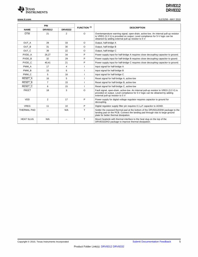
Pin Functions
PINFUNCTION (1) DESCRIPTION
NAME DRV8312 DRV8332
AGND 12 9 P Analog ground
BST_A 24 35 P High side bootstrap supply (BST), external capacitor to OUT_A required
BST_B 33 28 P High side bootstrap supply (BST), external capacitor to OUT_B required
BST_C 43 20 P High side bootstrap supply (BST), external capacitor to OUT_C required
GND 13, 36, 37 8 P Ground
GND_A 29 32 P Power ground for half-bridge A requires close decoupling capacitor to ground
GND_B 30 31 P Power ground for half-bridge B requires close decoupling capacitor to ground
GND_C 38 23 P Power ground for half-bridge C requires close decoupling capacitor to ground
GVDD_A 23 36 P Gate-drive voltage supply
GVDD_B 22 1 P Gate-drive voltage supply
GVDD_C 1, 44 18, 19 P Gate-drive voltage supply
M1 8 13 I Mode selection pin
M2 9 12 I Mode selection pin
M3 10 11 I Reserved mode selection pin, AGND connection is recommended
NC 3,4,19,20,25,34,35 26,27 - No connection pin. Ground connection is recommended,42
OC_ADJ 14 7 O Analog overcurrent programming pin, requires resistor to AGND
(1) I = input, O = output, P = power, T = thermal
4 Submit Documentation Feedback Copyright © 2010, Texas Instruments Incorporated
Product Folder Link(s): DRV8312 DRV8332
DRV8312DRV8332
www.ti.com SLES256 –MAY 2010
PINFUNCTION (1) DESCRIPTION
NAME DRV8312 DRV8332
OTW 21 2 O Overtemperature warning signal, open-drain, active-low. An internal pull-up resistorto VREG (3.3 V) is provided on output. Level compliance for 5-V logic can beobtained by adding external pull-up resistor to 5 V
OUT_A 28 33 O Output, half-bridge A
OUT_B 31 30 O Output, half-bridge B
OUT_C 39 22 O Output, half-bridge C
PVDD_A 26,27 34 P Power supply input for half-bridge A requires close decoupling capacitor to ground.
PVDD_B 32 29 P Power supply input for half-bridge B requires close decoupling capacitor to gound.
PVDD_C 40,41 21 P Power supply input for half-bridge C requires close decoupling capacitor to ground.
PWM_A 17 4 I Input signal for half-bridge A
PWM_B 15 6 I Input signal for half-bridge B
PWM_C 5 16 I Input signal for half-bridge C
RESET_A 16 5 I Reset signal for half-bridge A, active-low
RESET_B 7 15 I Reset signal for half-bridge B, active-low
RESET_C 6 15 I Reset signal for half-bridge C, active-low
FAULT 18 3 O Fault signal, open-drain, active-low. An internal pull-up resistor to VREG (3.3 V) isprovided on output. Level compliance for 5-V logic can be obtained by addingexternal pull-up resistor to 5 V
VDD 2 17 P Power supply for digital voltage regulator requires capacitor to ground fordecoupling.
VREG 11 10 P Digital regulator supply filter pin requires 0.1-mF capacitor to AGND.
THERMAL PAD -- N/A T Solder the exposed thermal pad at the bottom of the DRV8312DDW package to thelanding pad on the PCB. Connect the landing pad through vias to large groundplate for better thermal dissipation.
HEAT SLUG N/A -- T Mount heatsink with thermal interface to the heat slug on the top of theDRV8332DKD package to improve thermal dissipation.
Copyright © 2010, Texas Instruments Incorporated Submit Documentation Feedback 5
Product Folder Link(s): DRV8312 DRV8332
Temp.
Sense
M1
M2
RESET_A
FAULT
OTW
AGND
OC_ADJ
VREG VREG
VDD
M3
Power
On
Reset
Under-
voltage
Protection
GND
PWM_C OUT_C
GND_C
PVDD_C
BST_C
TimingGate
Drive
PWM
Rcv.
Overload
ProtectionIsense
GVDD_C
RESET_B
4
Protection
and
I/O Logic
PWM_B OUT_B
GND_B
PVDD_B
BST_B
TimingGate
DriveCtrl.
PWM
Rcv.
GVDD_B
PWM_A OUT_A
GND_A
PVDD_A
BST_A
TimingGate
DriveCtrl.
PWM
Rcv.
GVDD_A
Ctrl.
Internal Pullup
Resistors to VREG
4
RESET_C
DRV8312DRV8332
SLES256 –MAY 2010 www.ti.com
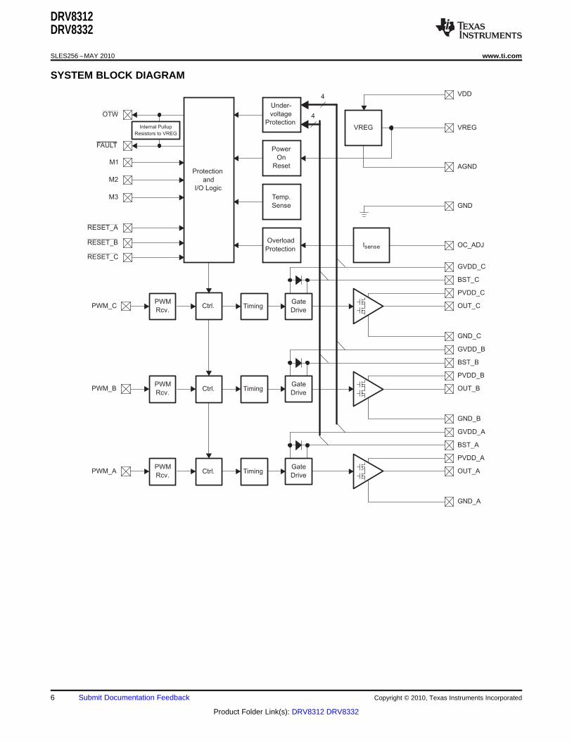
SYSTEM BLOCK DIAGRAM
6 Submit Documentation Feedback Copyright © 2010, Texas Instruments Incorporated
Product Folder Link(s): DRV8312 DRV8332

DRV8312DRV8332
www.ti.com SLES256 –MAY 2010
ELECTRICAL CHARACTERISTICSTA = 25 °C, PVDD = 50 V, GVDD = VDD = 12 V, fSw = 400 kHz, unless otherwise noted. All performance is in accordancewith recommended operating conditions unless otherwise specified.
PARAMETER TEST CONDITIONS MIN TYP MAX UNIT
Internal Voltage Regulator and Current Consumption
VREG Voltage regulator, only used as a reference node VDD = 12 V 2.95 3.3 3.65 V
Idle, reset mode 9 12 mAIVDD VDD supply current
Operating, 50% duty cycle 10.5
Reset mode 1.7 2.5 mAIGVDD_X Gate supply current per half-bridge
Operating, 50% duty cycle 8
IPVDD_X Half-bridge X (A, B, or C) idle current Reset mode 0.7 1 mA
Output Stage
MOSFET drain-to-source resistance, low side (LS) TJ = 25°C, GVDD = 12 V 80 mΩRDS(on)
MOSFET drain-to-source resistance, high side (HS) TJ = 25°C, GVDD = 12 V 80 mΩ
VF Diode forward voltage drop TJ = 25°C - 125°C, IO = 5 A 1 V
tR Output rise time Resistive load, IO = 5 A 14 nS
tF Output fall time Resistive load, IO = 5 A 14 nS
tPD_ON Propagation delay when FET is on Resistive load, IO = 5 A 38 nS
tPD_OFF Propagation delay when FET is off Resistive load, IO = 5 A 38 nS
tDT Dead time between HS and LS FETs Resistive load, IO = 5 A 5.5 nS
I/O Protection
Gate supply voltage GVDD_X undervoltageVuvp,G 8.5 Vprotection threshold
Vuvp,hyst(1) Hysteresis for gate supply undervoltage event 0.8 V
OTW (1) Overtemperature warning 115 125 135 °C
OTWhyst(1) Hysteresis temperature to reset OTW event 25 °C
OTSD (1) Overtemperature shut down 150 °C
OTE- OTE-OTW overtemperature detect temperature 25 °COTWdifferential(1) difference
Hysteresis temperature for FAULT to be releasedOTSDHYST(1) 25 °Cfollowing an OTSD event
IOC Overcurrent limit protection Resistor—programmable, nominal, ROCP = 27 kΩ 9.7 A
Time from application of short condition to Hi-Z ofIOCT Overcurrent response time 250 nsaffected FET(s)
Static Digital Specifications
VIH High-level input voltage PWM_A, PWM_B, PWM_C, M1, M2, M3 2 3.6 V
VIH High-level input voltage RESET_A, RESET_B, RESET_C 2 3.6 V
PWM_A, PWM_B, PWM_C, M1, M2, M3,VIL Low-level input voltage 0.8 VRESET_A, RESET_B, RESET_C
llkg Input leakage current -100 100 mA
OTW / FAULT
Internal pullup resistance, OTW to VREG, FAULT toRINT_PU 20 26 35 kΩVREG
Internal pullup resistor only 2.95 3.3 3.65VOH High-level output voltage V
External pullup of 4.7 kΩ to 5 V 4.5 5
VOL Low-level output voltage IO = 4 mA 0.2 0.4 V
(1) Specified by design
Copyright © 2010, Texas Instruments Incorporated Submit Documentation Feedback 7
Product Folder Link(s): DRV8312 DRV8332
1.10
0.96
1.00
0.98
1.02
1.04
GVDD – Gate Drive – V
No
rmalized
R/ (R
at
12 V
)D
S(o
n)
DS
(on
)11.010.08.0 10.59.58.5 9.0 11.5
1.06
1.08
12
T = 25°CJ
0
100
40
50
60
70
80
90
Eff
icie
ncy
–%
f – Switching Frequency – kHz
0 100 150 200 250 300 350 400 450 50050
10
20
30
Load = 5 APVDD = 50 VT = 75°C
Full Bridge
C
1.6
0.4
0.6
0.8
1.0
T – Junction Temperature – CJo
No
rmalized
R/ (R
at
25
C)
DS
(on
)D
S(o
n)
o
8040 120–40 6020–20 0 100
1.2
1.4
140
GVDD = 12 V
–1
5
0
1
2
3
V – Voltage – V
I–
Cu
rren
t–
A
1.20.80 10.60.2 0.4
4
6
T = 25°CJ
DRV8312DRV8332
SLES256 –MAY 2010 www.ti.com
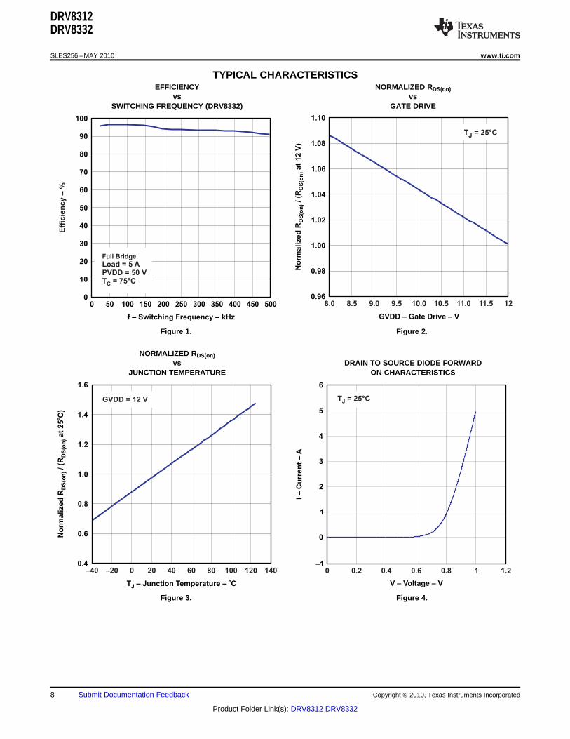
TYPICAL CHARACTERISTICSEFFICIENCY NORMALIZED RDS(on)
vs vsSWITCHING FREQUENCY (DRV8332) GATE DRIVE
Figure 1. Figure 2.
NORMALIZED RDS(on)vs DRAIN TO SOURCE DIODE FORWARD
JUNCTION TEMPERATURE ON CHARACTERISTICS
Figure 3. Figure 4.
8 Submit Documentation Feedback Copyright © 2010, Texas Instruments Incorporated
Product Folder Link(s): DRV8312 DRV8332
0
100
10
20
30
40
50
60
70
80
90
Ou
tpu
t D
uty
Cycle
–%
Input Duty Cycle – %
9060 1000 70402010 30 50 80
f = 500 kHz
T = 25°CS
C
DRV8312DRV8332
www.ti.com SLES256 –MAY 2010
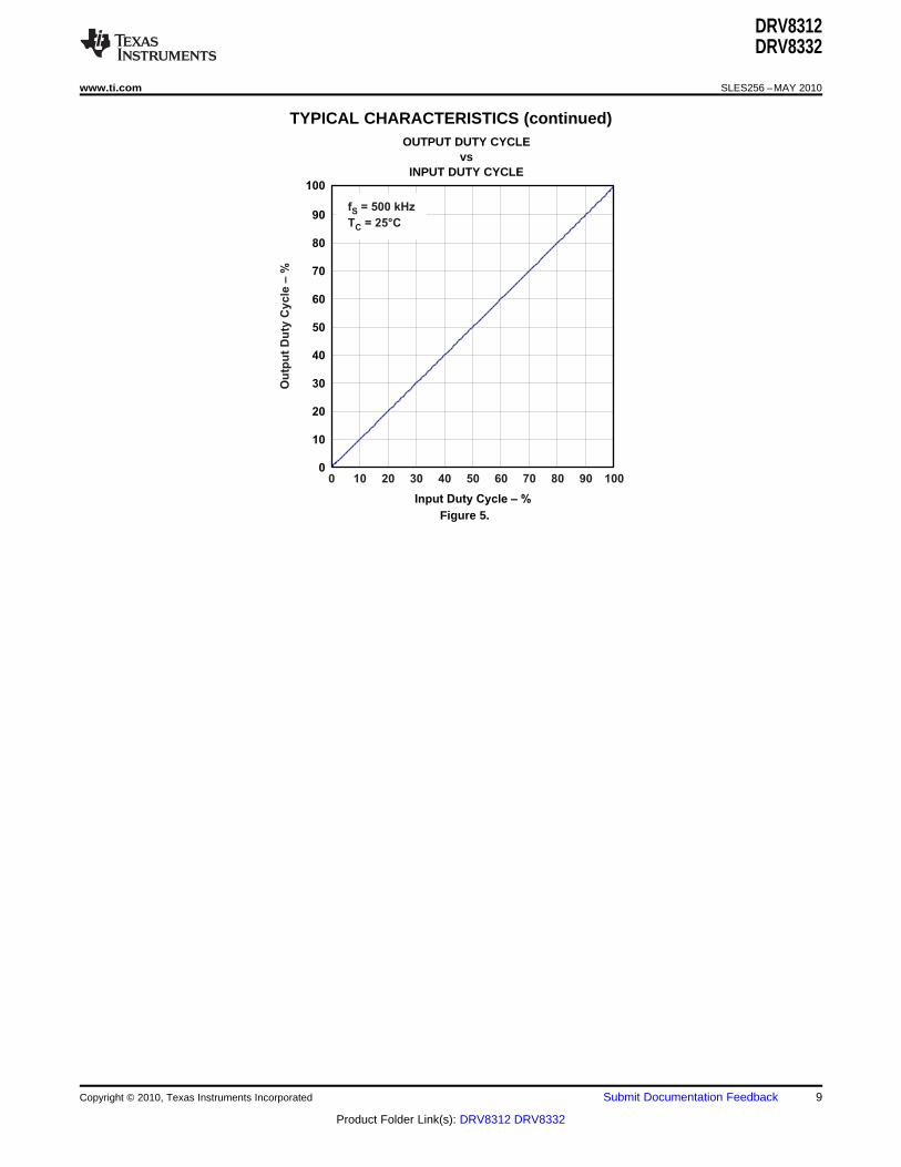
TYPICAL CHARACTERISTICS (continued)OUTPUT DUTY CYCLE
vsINPUT DUTY CYCLE
Figure 5.
Copyright © 2010, Texas Instruments Incorporated Submit Documentation Feedback 9
Product Folder Link(s): DRV8312 DRV8332
DRV8312DRV8332
SLES256 –MAY 2010 www.ti.com
THEORY OF OPERATION
Special attention should be paid to the power-stagePOWER SUPPLIES power supply; this includes component selection,PCB placement, and routing. As indicated, eachTo facilitate system design, the DRV8312/32 needhalf-bridge has independent power-stage supply pinonly a 12-V supply in addition to H-Bridge power(PVDD_X). For optimal electrical performance, EMIsupply (PVDD). An internal voltage regulator providescompliance, and system reliability, it is important thatsuitable voltage levels for the digital and low-voltageeach PVDD_X pin is decoupled with a ceramicanalog circuitry. Additionally, the high-side gate drivecapacitor (X5R or better) placed as close as possiblerequiring a floating voltage supply, which isto each supply pin. It is recommended to follow theaccommodated by built-in bootstrap circuitry requiringPCB layout of the DRV8312/32 EVM board.external bootstrap capacitor.
The 12-V supply should be from a low-noise,To provide symmetrical electrical characteristics, thelow-output-impedance voltage regulator. Likewise, thePWM signal path, including gate drive and output50-V power-stage supply is assumed to have lowstage, is designed as identical, independentoutput impedance and low noise. The power-supplyhalf-bridges. For this reason, each half-bridge has asequence is not critical as facilitated by the internalseparate gate drive supply (GVDD_X), a bootstrappower-on-reset circuit. Moreover, the DRV8312/32pin (BST_X), and a power-stage supply pinare fully protected against erroneous power-stage(PVDD_X). Furthermore, an additional pin (VDD) isturn-on due to parasitic gate charging. Thus,provided as supply for all common circuits. Specialvoltage-supply ramp rates (dv/dt) are non-criticalattention should be paid to place all decouplingwithin the specified voltage range (see thecapacitors as close to their associated pins asRecommended Operating Conditions section of thispossible. In general, inductance between the powerdata sheet).supply pins and decoupling capacitors must be
avoided. Furthermore, decoupling capacitors need ashort ground path back to the device. SYSTEM POWER-UP/POWER-DOWN
SEQUENCEFor a properly functioning bootstrap circuit, a smallceramic capacitor (an X5R or better) must be Powering Upconnected from each bootstrap pin (BST_X) to thepower-stage output pin (OUT_X). When the The DRV8312/32 do not require a power-uppower-stage output is low, the bootstrap capacitor is sequence. The outputs of the H-bridges remain in acharged through an internal diode connected high impedance state until the gate-drive supplybetween the gate-drive power-supply pin (GVDD_X) voltage GVDD_X and VDD voltage are above theand the bootstrap pin. When the power-stage output undervoltage protection (UVP) voltage threshold (seeis high, the bootstrap capacitor potential is shifted the Electrical Characteristics section of this dataabove the output potential and thus provides a sheet). Although not specifically required, holdingsuitable voltage supply for the high-side gate driver. RESET_A, RESET_B, and RESET_C in a low stateIn an application with PWM switching frequencies in while powering up the device is recommended. Thisthe range from 10 kHz to 500 kHz, the use of 100-nF allows an internal circuit to charge the externalceramic capacitors (X5R or better), size 0603 or bootstrap capacitors by enabling a weak pulldown of0805, is recommended for the bootstrap supply. the half-bridge output.These 100-nF capacitors ensure sufficient energystorage, even during minimal PWM duty cycles, to Powering Downkeep the high-side power stage FET fully turned on
The DRV8312/32 do not require a power-downduring the remaining part of the PWM cycle. In ansequence. The device remains fully operational asapplication running at a switching frequency lowerlong as the gate-drive supply (GVDD_X) voltage andthan 10 kHz, the bootstrap capacitor might need to beVDD voltage are above the UVP voltage thresholdincreased in value.(see the Electrical Characteristics section of this datasheet). Although not specifically required, it is a goodpractice to hold RESET_A, RESET_B and RESET_Clow during power down to prevent any unknown stateduring this transition.
10 Submit Documentation Feedback Copyright © 2010, Texas Instruments Incorporated
Product Folder Link(s): DRV8312 DRV8332
DRV8312DRV8332
www.ti.com SLES256 –MAY 2010
Bootstrap Capacitor Under Voltage ProtectionERROR REPORTINGWhen the device runs at a low switching frequencyThe FAULT and OTW pins are both active-low,(e.g. less than 10 kHz with a 100-nF bootstrapopen-drain outputs. Their function is forcapacitor), the bootstrap capacitor voltage might notprotection-mode signaling to a PWM controller orbe able to maintain a proper voltage level for theother system-control device.high-side gate driver. A bootstrap capacitor
Any fault resulting in device shutdown, such as undervoltage protection circuit (BST_UVP) willovertemperatue shut down, overcurrent shut-down, or prevent potential failure of the high-side MOSFET.undervoltage protection, is signaled by the FAULT pin When the voltage on the bootstrap capacitors is lessgoing low. Likewise, OTW goes low when the device than the required value for safe operation, thejunction temperature exceeds 125°C (see Table 1). DRV8312/32 will initiate bootstrap capacitor recharge
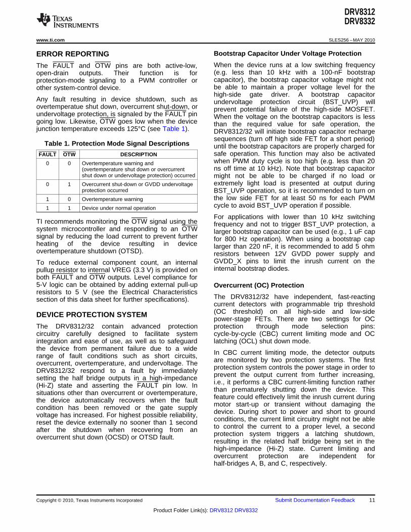
sequences (turn off high side FET for a short period)Table 1. Protection Mode Signal Descriptions until the bootstrap capacitors are properly charged for
safe operation. This function may also be activatedFAULT OTW DESCRIPTIONwhen PWM duty cycle is too high (e.g. less than 200 0 Overtemperature warning andns off time at 10 kHz). Note that bootstrap capacitor(overtemperature shut down or overcurrent
shut down or undervoltage protection) occurred might not be able to be charged if no load orextremely light load is presented at output during0 1 Overcurrent shut-down or GVDD undervoltage
protection occurred BST_UVP operation, so it is recommended to turn onthe low side FET for at least 50 ns for each PWM1 0 Overtemperature warningcycle to avoid BST_UVP operation if possible.1 1 Device under normal operation
For applications with lower than 10 kHz switchingTI recommends monitoring the OTW signal using the frequency and not to trigger BST_UVP protection, asystem microcontroller and responding to an OTW larger bootstrap capacitor can be used (e.g., 1 uF capsignal by reducing the load current to prevent further for 800 Hz operation). When using a bootstrap capheating of the device resulting in device larger than 220 nF, it is recommended to add 5 ohmovertemperature shutdown (OTSD). resistors between 12V GVDD power supply and
GVDD_X pins to limit the inrush current on theTo reduce external component count, an internalinternal bootstrap diodes.pullup resistor to internal VREG (3.3 V) is provided on
both FAULT and OTW outputs. Level compliance for5-V logic can be obtained by adding external pull-up Overcurrent (OC) Protectionresistors to 5 V (see the Electrical Characteristics
The DRV8312/32 have independent, fast-reactingsection of this data sheet for further specifications).current detectors with programmable trip threshold(OC threshold) on all high-side and low-sideDEVICE PROTECTION SYSTEMpower-stage FETs. There are two settings for OC
The DRV8312/32 contain advanced protection protection through mode selection pins:circuitry carefully designed to facilitate system cycle-by-cycle (CBC) current limiting mode and OCintegration and ease of use, as well as to safeguard latching (OCL) shut down mode.the device from permanent failure due to a wide
In CBC current limiting mode, the detector outputsrange of fault conditions such as short circuits,are monitored by two protection systems. The firstovercurrent, overtemperature, and undervoltage. Theprotection system controls the power stage in order toDRV8312/32 respond to a fault by immediatelyprevent the output current from further increasing,setting the half bridge outputs in a high-impedancei.e., it performs a CBC current-limiting function rather(Hi-Z) state and asserting the FAULT pin low. Inthan prematurely shutting down the device. Thissituations other than overcurrent or overtemperature,feature could effectively limit the inrush current duringthe device automatically recovers when the faultmotor start-up or transient without damaging thecondition has been removed or the gate supplydevice. During short to power and short to groundvoltage has increased. For highest possible reliability,conditions, the current limit circuitry might not be ablereset the device externally no sooner than 1 secondto control the current to a proper level, a secondafter the shutdown when recovering from anprotection system triggers a latching shutdown,overcurrent shut down (OCSD) or OTSD fault.resulting in the related half bridge being set in thehigh-impedance (Hi-Z) state. Current limiting andovercurrent protection are independent forhalf-bridges A, B, and C, respectively.
Copyright © 2010, Texas Instruments Incorporated Submit Documentation Feedback 11
Product Folder Link(s): DRV8312 DRV8332
DRV8312DRV8332
SLES256 –MAY 2010 www.ti.com
Figure 6 illustrates cycle-by-cycle operation with high It should be noted that a properly functioningside OC event and Figure 7 shows cycle-by-cycle overcurrent detector assumes the presence of aoperation with low side OC. Dashed lines are the proper inductor or power ferrite bead at theoperation waveforms when no CBC event is triggered power-stage output. Short-circuit protection is notand solide lines show the waveforms when CBC guaranteed with direct short at the output pins of theevent is triggered. In CBC current limiting mode, power stage.when low side FET OC is detected, devcie will turnoff the affected low side FET and keep the high side Overtemperature ProtectionFET at the same half brdige off until next PWM cycle;
The DRV8312/32 have a two-levelwhen high side FET OC is detected, devcie will turntemperature-protection system that asserts anoff the affected high side FET and turn on the lowactive-low warning signal (OTW) when the deviceside FET at the half brdige until next PWM cycle.junction temperature exceeds 125°C (nominal) and, if
In OC latching shut down mode, the CBC current limit the device junction temperature exceeds 150°Cand error recovery circuitries are disabled and an (nominal), the device is put into thermal shutdown,overcurrent condition will cause the device to resulting in all half-bridge outputs being set in theshutdown immediately. After shutdown, RESET_A, high-impedance (Hi-Z) state and FAULT beingRESET_B, and / or RESET_C must be asserted to asserted low. OTSD is latched in this case andrestore normal operation after the overcurrent RESET_A, RESET_B, and RESET_C must becondition is removed. asserted low to clear the latch.
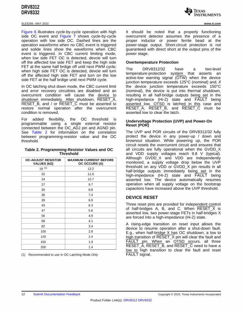
For added flexibility, the OC threshold is Undervoltage Protection (UVP) and Power-Onprogrammable using a single external resistor Reset (POR)connected between the OC_ADJ pin and AGND pin.
The UVP and POR circuits of the DRV8312/32 fullySee Table 2 for information on the correlationprotect the device in any power-up / down andbetween programming-resistor value and the OCbrownout situation. While powering up, the PORthreshold.circuit resets the overcurrent circuit and ensures thatall circuits are fully operational when the GVDD_XTable 2. Programming-Resistor Values and OC
Threshold and VDD supply voltages reach 9.8 V (typical).Although GVDD_X and VDD are independentlyOC-ADJUST RESISTOR MAXIMUM CURRENT BEFOREmonitored, a supply voltage drop below the UVPVALUES (kΩ) OC OCCURS (A)threshold on any VDD or GVDD_X pin results in all
19 (1) 13.2half-bridge outputs immediately being set in the
22 11.6 high-impedance (Hi-Z) state and FAULT being24 10.7 asserted low. The device automatically resumes
operation when all supply voltage on the bootstrap27 9.7capacitors have increased above the UVP threshold.30 8.8
36 7.4DEVICE RESET
39 6.9Three reset pins are provided for independent control43 6.3of half-bridges A, B, and C. When RESET_X is47 5.8asserted low, two power-stage FETs in half-bridges X
56 4.9 are forced into a high-impedance (Hi-Z) state.68 4.1
A rising-edge transition on reset input allows the82 3.4
device to resume operation after a shut-down fault.100 2.8 E.g., when half-bridge X has OC shutdown, a low to120 2.4 high transition of RESET_X pin will clear the fault and
FAULT pin. When an OTSD occurs, all three150 1.9RESET_A, RESET_B, and RESET_C need to have a200 1.4low to high transition to clear the fault and reset
(1) Recommended to use in OC Latching Mode Only FAULT signal.
12 Submit Documentation Feedback Copyright © 2010, Texas Instruments Incorporated
Product Folder Link(s): DRV8312 DRV8332

PWM_HS
PWM_LS
Load
Current
Current Limit
T_HS T_OC
PVDD
GND_X
PWM_HS
PWM_LS
Load
T_LS
CBC with High Side OCDuring T_OC Period
DRV8312DRV8332
www.ti.com SLES256 –MAY 2010
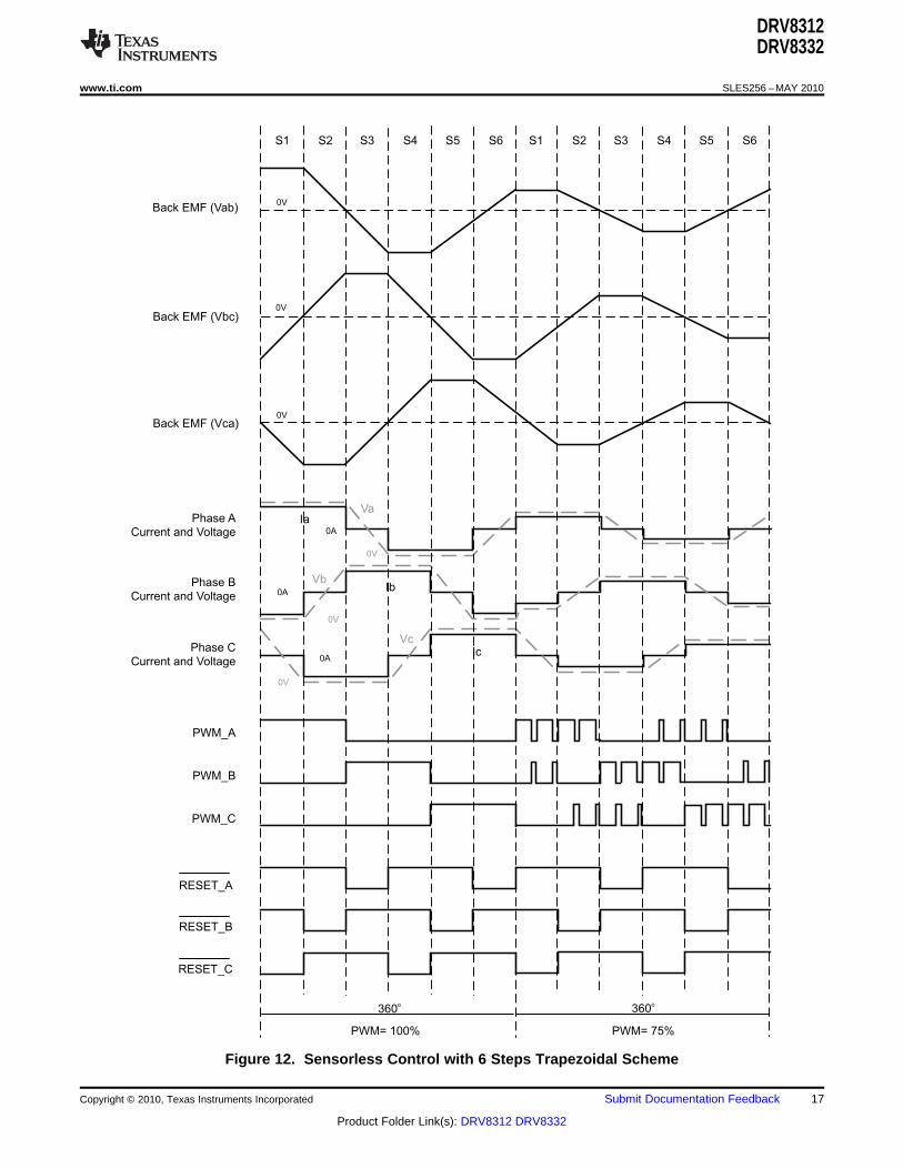
DIFFERENT OPERATIONAL MODES Figure 11 shows six steps trapezoidal scheme withhall sensor control and Figure 12 shows six steps
The DRV8312/32 support two different modes of trapezoidal scheme with sensorless control. The halloperation: sensor sequence in real application might be different1. Three-phase (3PH) or three half bridges (HB) than the one we showed in Figure 11 depending on
with CBC current limit the motor used. Please check motor manufacturedatasheet for the right sequence in applications. In2. Three-phase or three half bridges with OCsix step trapezoidal complementary control scheme, alatching shutdown (no CBC current limit)half bridge with larger than 50% duty cycle will have apositive current and a half bridge with less than 50%Because each half bridge has independent supplyduty cycle will have a negative current. For normaland ground pins, a shunt sensing resistor can beoperation, changing PWM duty cycle from 50% toinserted between PVDD to PVDD_X or GND_X to100% will adjust the current from 0 to maximum valueGND (ground plane). A high side shunt resistorwith six steps control. It is recommanded to apply abetween PVDD and PVDD_X is recommended forminimum 50ns to 100 nS PWM pulse at eachdifferential current sensing because a high biasswitching cycle at lower side to properly charge thevoltage on the low side sensing could affect devicebootstrap cap. The impact of minimum pulse at lowoperation. If low side sensing has to be used, a shuntside FET is pretty small, e.g., the maximum dutyresistor value of 10 mΩ or less or sense voltage 100cycle is 99.9% with 100ns minimum pulse on lowmV or less is recommended.side. RESET_Xpin can be used to get channel X into
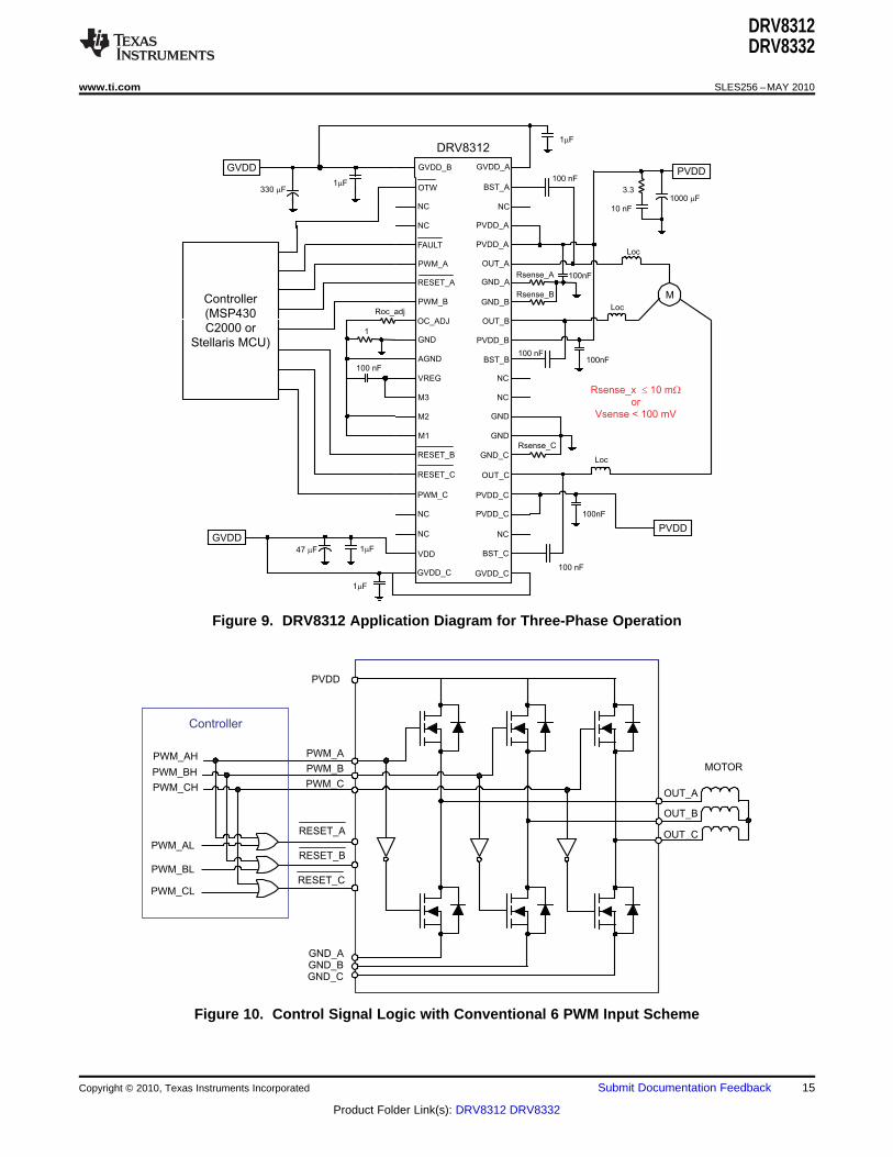
Figure 8 and Figure 9 show the three-phase high impedance mode. If you prefer PWM switchingapplication examples, and Figure 10 shows how to one channel but hold low side FET of the otherconnect to DRV8312/32 with some simple logic to channel on (and third channel in Hi-Z) for 2-quadrantaccommodate conventional 6 PWM inputs control. mode, OT latching shutdown mode is recommended
to prevent the channel with low side FET on stuck inWe recommend using complementary controlHi-Z during OC event in CBC mode.scheme for switching phases to prevent circulated
energy flowing inside the phases and to make currentThe DRV8312/32 can also be used for sinusoidallimiting feature active all the time. Complementarywaveform control and field oriented control. Pleasecontrol scheme also forces the current flowingcheck TI website MCU motor control library forthrough sense resistors all the time to have a bettercontrol algorithms.current sensing and control of the system.
Figure 6. Cycle-by-Cycle Operation with High Side OC (dashed line: normal operation; solid line: CBCevent)
Copyright © 2010, Texas Instruments Incorporated Submit Documentation Feedback 13
Product Folder Link(s): DRV8312 DRV8332

PWM_HS
PWM_LS
Load
Current
Current Limit
CBC with Low Side OC
T_LS T_OC
PVDD
GND_X
During T_OC Period
PWM_HS
PWM_LS
Load
T_HS
GVDD
GVDD
PVDD
PVDD
1000 Fm
Loc
Loc
Loc
3.3
10 nF
100 nF
100 nF
100 nF
1 Fm
1 Fm
1 Fm
100 nF
47 Fm
330 Fm
Roc_adj
Controller
(MSP430
C2000 or
Stellaris MCU)
RESET_A
PWM_B
OC_ADJ
GND
GND_A
GND_B
OUT_B
PVDD_B
AGND
VREG
M3
M2
BST_B
NC
NC
GND
RESET_C
PWM_C
VDD
GVDD_C
OUT_C
PVDD_C
BST_C
GVDD_C
RESET_B GND_C
M1 GND
GVDD_B
OTW
FAULT
PWM_A
GVDD_A
BST_A
PVDD_A
OUT_A
100nF
100nF
100nF
MRsense_B
Rsense_C
Rsense_A
1
Rsense_x
or
Vsense < 100 mV
£ 10 mW
DRV83321 Fm
DRV8312DRV8332
SLES256 –MAY 2010 www.ti.com
Figure 7. Cycle-by-Cycle Operation with Low Side OC (dashed line: normal operation; solid line: CBCevent)
Figure 8. DRV8332 Application Diagram for Three-Phase Operation
14 Submit Documentation Feedback Copyright © 2010, Texas Instruments Incorporated
Product Folder Link(s): DRV8312 DRV8332
OTW BST_A
GVDD
GVDD
PVDD
PVDD
1000 Fm
Loc
Loc
Loc
3.3
10 nF
100 nF
100 nF
100 nF
1 Fm
1 Fm
1 Fm
47 Fm
330 Fm
Controller
(MSP430
C2000 or
Stellaris MCU)
RESET_A
PWM_B
OC_ADJ
GND
GND_A
GND_B
OUT_B
PVDD_B
AGND
VREG
M3
M2
BST_B
NC
NC
GND
RESET_C
PWM_C
NC
NC
OUT_C
PVDD_C
PVDD_C
NC
RESET_B GND_C
M1 GND
NC
NC
FAULT
PWM_A
NC
PVDD_A
PVDD_A
OUT_A
100nF
100nF
100nF
MRsense_B
Rsense_C
Rsense_A
Rsense_x
or
Vsense < 100 mV
£ 10 mW
GVDD_B GVDD_A
VDD BST_C
GVDD_C GVDD_C
DRV8312
100 nF
Roc_adj
1
1 Fm
PVDD
OUT_A
PWM_A
PWM_B
OUT_CRESET_A
GND_A
MOTOR
PWM_C
GND_BGND_C
RESET_C
RESET_B
PWM_AH
PWM_CH
PWM_BH
PWM_AL
PWM_CL
PWM_BL
Controller
OUT_B
DRV8312DRV8332
www.ti.com SLES256 –MAY 2010
Figure 9. DRV8312 Application Diagram for Three-Phase Operation
Figure 10. Control Signal Logic with Conventional 6 PWM Input Scheme
Copyright © 2010, Texas Instruments Incorporated Submit Documentation Feedback 15
Product Folder Link(s): DRV8312 DRV8332

PWM_A
PWM_B
PWM_C
Phase Current A
Phase Current B
Phase Current C
Hall Sensor H1
Hall Sensor H2
Hall Sensor H3
S1 S6S5S4S3S2 S1 S6S5S4S3S2
PWM= 100% PWM=75%
360o
360o
RESET_A
RESET_B
RESET_C
DRV8312DRV8332
SLES256 –MAY 2010 www.ti.com
Figure 11. Hall Sensor Control with 6 Steps Trapezoidal Scheme
16 Submit Documentation Feedback Copyright © 2010, Texas Instruments Incorporated
Product Folder Link(s): DRV8312 DRV8332
PWM_A
PWM_B
PWM_C
Phase A
Current and Voltage
Phase B
Current and Voltage
Phase C
Current and Voltage
Back EMF (Vab)
Ia
Ib
Ic
Va
Vb
Vc
PWM= 100% PWM= 75%
S1 S6S5S4S3S2 S1 S6S5S4S3S2
Back EMF (Vbc)
Back EMF (Vca)
360o
360o
0V
0V
0V
0A
0A
0A
0V
0V
0V
RESET_A
RESET_B
RESET_C
DRV8312DRV8332
www.ti.com SLES256 –MAY 2010
Figure 12. Sensorless Control with 6 Steps Trapezoidal Scheme
Copyright © 2010, Texas Instruments Incorporated Submit Documentation Feedback 17
Product Folder Link(s): DRV8312 DRV8332
DRV8312DRV8332
SLES256 –MAY 2010 www.ti.com
APPLICATION INFORMATION
SYSTEM DESIGN RECOMMENDATIONS
Voltage of Decoupling Capacitor
The voltage of the decoupling capacitors should be selected in accordance with good design practices.Temperature, ripple current, and voltage overshoot must be considered. The high frequency decoupling capacitorshould use ceramic capacitor with X5R or better rating. For a 50-V application, a minimum voltage rating of 63 Vis recommended.
Current Requirement of 12V Power Supply
The DRV8312/32 require a 12V power supply for GVDD and VDD pins. The total supply current is pretty low atroom temp (less than 50mA), but the current could increase significantly when the device temperature goes toohigh (e.g. above 125°C), especially at heave load conditions due to substrate current collection by 12V guardrings. So it is recommended to design the 12V power supply with current capability at least 5-10% of your loadcurrent and no less than 100mA to assure the device performance across all temperature range.
VREG Pin
The VREG pin is used for internal logic and should not be used as a voltage source for external circuitries. Thecapacitor on VREG pin should be connected to AGND.
VDD Pin
The transient current in VDD pin could be significantly higher than average current through VDD pin. A lowresistive path to GVDD should be used. A 22-µF to 47-µF capacitor should be placed on VDD pin beside the100-nF to 1-µF decoupling capacitor to provide a constant voltage during transient.
OTW Pin
OTW reporting indicates the device approaching high junction temperature. This signal can be used with MCU todecrease system power when OTW is low in order to prevent OT shut down at a higher temperature.
No external pull up resistor or 3.3V power supply is needed for 3.3V logic. The OTW pin has an internal pullupresistor connecting to an internal 3.3V to reduce external component count. For 5V logic, an external pull upresistor to 5V is needed.
FAULT Pin
The FAULT pin reports any fault condition resulting in device shut down. No external pull up resistor or 3.3Vpower supply is needed for 3.3V logic. The FAULT pin has an internal pullup resistor connecting to an internal3.3V to reduce external component count. For 5V logic, an external pull upresistor to 5V is needed.
OC_ADJ Pin
For accurate control of the oevercurrent protection, the OC_ADJ pin has to be connected to AGND through anOC adjust resistor.
PWM_X and RESET_X Pins
It is recommanded to connect these pins to either AGND or GND when they are not used, and these pins onlysupport 3.3V logic.
Mode Select Pins
Mode select pins (M1, M2, and M3) should be connected to either VREG (for logic high) or AGND for logic low. Itis not recommended to connect mode pins to board ground if 1-Ω resistor is used between AGND and GND.
18 Submit Documentation Feedback Copyright © 2010, Texas Instruments Incorporated
Product Folder Link(s): DRV8312 DRV8332
__min
PVDD Toc delayLoc
Ipeak Iave
×
=
-
DRV8312DRV8332
www.ti.com SLES256 –MAY 2010
Output Inductor Selection
For normal operation, inductance in motor (assume larger than 10 µH) is sufficient to provide low di/dt output(e.g. for EMI) and proper protection during overload condition (CBC current limiting feature). So no additionaloutput inductors are needed during normal operation.
However during a short condition, the motor (or other load) could be shorted, so the load inductance might notpresent in the system anymore; the current in short condition can reach such a high level that may exceed theabs max current rating due to extremely low impendence in the short circuit path and high di/dt before ocdetection circuit kicks in. So a ferrite bead or inductor is recommended to utilize the short circuit protectionfeature in DRV8312/32. With an external inductor or ferrite bead, the current will rise at a much slower rate andreach a lower current level before oc protection starts. The device will then either operate CBC current limit orOC shut down automatically (when current is well above the current limit threshold) to protect the system.
For a system that has limited space, a power ferrite bead can be used instead of an inductor. The current ratingof ferrite bead has to be higher than the RMS current of the system at normal operation. A ferrite bead designedfor very high frequency is NOT recommended. A minimum impedance of 10 Ω or higher is recommended at 10MHz or lower frequency to effectively limit the current rising rate during short circuit condition.
The TDK MPZ2012S300A and MPZ2012S101A (with size of 0805 inch type) have been tested in our system tomeet short circuit conditions in the DRV8312. But other ferrite beads that have similar frequency characteristicscan be used as well.
For higher power applications, such as in the DRV8332, there might be limited options to select suitable ferritebead with high current rating. If an adequate ferrite bead cannot be found, an inductor can be used.
The inductance can be calculated as:
(1)
Where Toc_delay = 250 nS, Ipeak = 15 A (below abs max rating).
Because an inductor usually saturates pretty quickly after reaching its current rating, it is recommended to use aninductor with a doubled value or an inductor with a current rating well above the operating condition.
PCB LAYOUT RECOMMENDATION
PCB Material Recommendation
FR-4 Glass Epoxy material with 2 oz. copper on both top and bottom layer is recommended for improved thermalperformance (better heat sinking) and less noise susceptibility (lower PCB trace inductance).
Ground Plane
Because of the power level of these devices, it is recommended to use a big unbroken single ground plane forthe whole system / board. The ground plane can be easily made at bottom PCB layer. In order to minimize theimpedance and inductance of ground traces, the traces from ground pins should keep as short and wide aspossible before connected to bottom ground plane through vias. Multiple vias are suggested to reduce theimpedance of vias. Try to clear the space around the device as much as possible especially at bottom PCB sideto improve the heat spreading.
Decoupling Capacitor
High frequency decoupling capacitors (100 nF) should be placed close to PVDD_X pins and with a short groundreturn path to minimize the inductance on the PCB trace.
AGND
AGND is a localized internal ground for logic signals. A 1-Ω resistor is recommended to be connected betweenGND and AGND to isolate the noise from board ground to AGND. There are other two components areconnected to this local ground: 0.1-µF capacitor between VREG to AGND and Roc_adj resistor betweenOC_ADJ and AGND. Capacitor for VREG should be placed close to VREG and AGND pins and connectedwithout vias.
Copyright © 2010, Texas Instruments Incorporated Submit Documentation Feedback 19
Product Folder Link(s): DRV8312 DRV8332
DRV8312DRV8332
SLES256 –MAY 2010 www.ti.com
Current Shunt Resistor
If current shunt resistor is connected between GND_X to GND or PVDD_X to PVDD, make sure there is only onesingle path to connect each GND_X or PVDD_X pin to shunt resistor, and the path is short and symmetrical oneach sense path to minimize the measurement error due to additional resistance on the trace.
PCB LAYOUT EXAMPLE
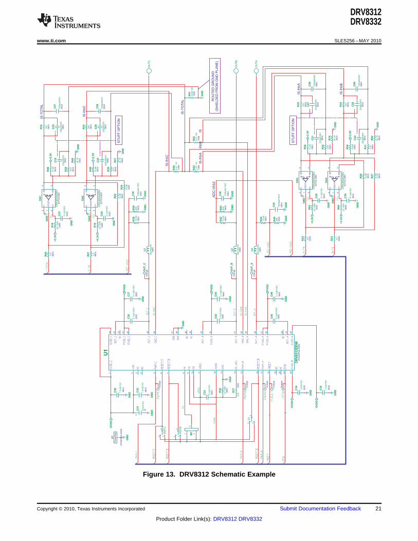
An example of the schematic and PCB layout of DRV8312 are shown in Figure 13, Figure 14, and Figure 15.
20 Submit Documentation Feedback Copyright © 2010, Texas Instruments Incorporated
Product Folder Link(s): DRV8312 DRV8332
GN
D
GN
D
GN
D
Ora
ng
e
Ora
ng
e
Ora
ng
e
Ora
ng
e
Ora
ng
e
GN
D
GN
D
GV
DD
GN
D
GV
DD
GV
DD
GN
D
GN
D
GN
DG
ND
0.1
ufd
/10
0V
08
05
C37
0.1
ufd
/10
0V
08
05
C43
0.1
ufd
/10
0V
08
05
C46
23 1
S1
132
RS
TB
47
K0
60
3
R37
0.1
ufd
/16
V
06
03
C33 1
.0u
fd/1
6V
06
03
C35
1.0
ufd
/16
V
06
03
C34
1.0
ufd
/16
V
06
03
C30
30
oh
ms/6
A0
80
5
L2
30
oh
ms/6
A0
80
5
L3
30
oh
ms/6
A0
80
5
L4
47
ufd
/16
VMC
31
+
1.0
ufd
/16
V
06
03
C32
PV
DD
49
90
60
3
R39
10
00
pfd
/10
0V
06
03
C50
GN
DG
ND
PV
DD
PV
DD
OU
TC
OU
TB
OU
TA
10
.0K
06
03
R38
49
90
60
3
R43
10
00
pfd
/10
0V
06
03
C56
GN
DG
ND
10
.0K
06
03
R42
49
90
60
3
R45
10
00
pfd
/10
0V
06
03
C55
10
.0K
06
03
R44
+3.3
V
GN
D
0.1
ufd
/16
V
06
03
C23
33
1/8
W0
80
5
R18
93
10
60
3
R34
93
10
60
3
R35
61
90
60
3
R29
61
90
60
3
R30
93
10
60
3
R33
0.0
06
03
R21
0.0
06
03
R22
0.0
06
03
R23
1.0
1/4
W0
80
5
R36
0.1
ufd
/10
0V
08
05
C36
0.1
ufd
/10
0V
08
05
C42
0.1
ufd
/10
0V
08
05
C45
61
90
60
3
R31
Ora
ng
eOU
T_C
Ora
ng
eOU
T_B
Ora
ng
eOU
T_A
0.0
11
W1
20
6
R50
15
.4K
06
03
R49
15
.4K
06
03
R55
15
.4K
06
03
R54
22
0p
fd/5
0V
06
03
C20
22
0p
fd/5
0V
06
03
C21
22
0p
fd/5
0V
06
03
C22
22
0p
fd/5
0V
06
03
C27
22
0p
fd/5
0V
06
03
C26
22
0p
fd/5
0V
06
03
C28
10
.2K
06
03
R25
10
.2K
06
03
R26
10
.2K
06
03
R27
10
00
pfd
/50
V0
60
3
C60
GN
DG
ND
10
00
pfd
/50
V0
60
3
C59
10
00
pfd
/50
V0
60
3
C58
HT
SS
OP
44
-DD
W
1 2 3 4 5 6 7 8 9 10
11
12
13
14
15
16
17
18
19
20
21
22
23
24
25
26
27
28
29
30
31
32
33
34
35
36
37
38
39
40
41
42
43
44
DR
V8312D
DW
U1
HT
SS
OP
44
-DD
W
U1
Po
we
rPa
d
GN
D
61
90
60
3
R28
93
10
60
3
R32
15
.4K
06
03
R48
22
0p
fd/5
0V
06
03
C19
22
0p
fd/5
0V
06
03
C25
10
00
pfd
/50
V0
60
3
C57
1
2
3M1
23 1
RS
TC
0.0
11
W1
20
6
R53
0.0
11
W1
20
6
R52
GN
D
0.0
05
1W
12
06
R51
10
.2K
06
03
R24
0.0
06
03
R20
30
.1K
06
03
R41
GN
D
30
.1K
06
03
R40
GN
D
+2.5
V
+2.5
V
+2.5
V
+2.5
V
30
.1K
06
03
R16
GN
D
30
.1K
06
03
R62
GN
D
SO
T2
3-D
BV
2 1 5
4 3
OP
A365A
IDB
V
OA
1
+IN-IN
V-
VO
UT
V+
GN
D
OA
2
OP
A365A
IDB
V
34
512
SO
T2
3-D
BV+
IN-IN
V-
VO
UT
V+
+3.3
V
GN
DGN
D
V-
SO
T2
3-D
BV
2 1 5
4 3
OP
A365A
IDB
V
OA
3
+IN-IN
VO
UT
V+
+3.3
V
GN
D
0.1
ufd
/16
V
06
03
C29
33
1/8
W0
80
5
R63
GN
D
R19
08
05
33
1/8
WC
24
06
03
0.1
ufd
/16
V
OA
4
OP
A365A
IDB
V
34
512
SO
T2
3-D
BV
V-
+IN-IN
VO
UT
V+
+3.3
V
GN
D
C39
06
03
0.1
ufd
/16
V
R64
08
05
33
1/8
W
GN
D
ST
UF
FO
PT
ION
ST
UF
FO
PT
ION
RO
UT
ED
GR
OU
ND
(SH
IEL
DE
DF
RO
MG
ND
PLA
NE
)
IS-I
hb
B
IS-I
hb
A
IS-I
hb
C
AD
C-V
hb2
IS-T
OTA
L
IS-I
hb
AIS
-Ih
bB
IS-I
hb
C
IS-T
OTA
L
DRV8312DRV8332
www.ti.com SLES256 –MAY 2010
Figure 13. DRV8312 Schematic Example
Copyright © 2010, Texas Instruments Incorporated Submit Documentation Feedback 21
Product Folder Link(s): DRV8312 DRV8332
C3
7
C33T1
T2
T3
T4
C4
6
C43
B1
DRV8312DRV8332
SLES256 –MAY 2010 www.ti.com
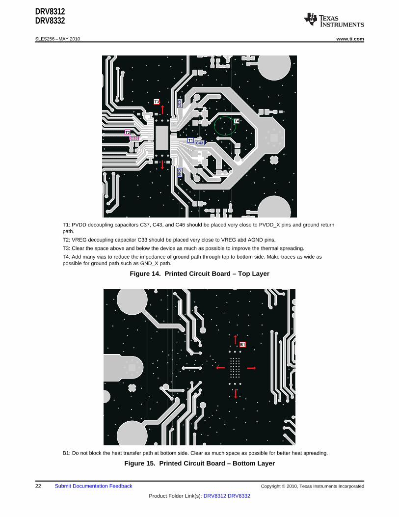
T1: PVDD decoupling capacitors C37, C43, and C46 should be placed very close to PVDD_X pins and ground returnpath.
T2: VREG decoupling capacitor C33 should be placed very close to VREG abd AGND pins.
T3: Clear the space above and below the device as much as possible to improve the thermal spreading.
T4: Add many vias to reduce the impedance of ground path through top to bottom side. Make traces as wide aspossible for ground path such as GND_X path.
Figure 14. Printed Circuit Board – Top Layer
B1: Do not block the heat transfer path at bottom side. Clear as much space as possible for better heat spreading.
Figure 15. Printed Circuit Board – Bottom Layer
22 Submit Documentation Feedback Copyright © 2010, Texas Instruments Incorporated
Product Folder Link(s): DRV8312 DRV8332
DRV8312DRV8332
www.ti.com SLES256 –MAY 2010
THERMAL INFORMATION
The thermally enhanced package provided with the DRV8332 is designed to interface directly to heat sink usinga thermal interface compound in between, (e.g., Ceramique from Arctic Silver, TIMTronics 413, etc.). The heatsink then absorbs heat from the ICs and couples it to the local air. It is also a good practice to connect theheatsink to system ground on the PCB board to reduce the ground noise.
RqJA is a system thermal resistance from junction to ambient air. As such, it is a system parameter with thefollowing components:• RqJC (the thermal resistance from junction to case, or in this example the power pad or heat slug)• Thermal grease thermal resistance• Heat sink thermal resistance
The thermal grease thermal resistance can be calculated from the exposed power pad or heat slug area and thethermal grease manufacturer's area thermal resistance (expressed in °C-in 2/W or °C-mm2/W). The approximateexposed heat slug size is as follows:• DRV8332, 36-pin PSOP3 …… 0.124 in2 (80 mm 2)
The thermal resistance of a thermal pad is considered higher than a thin thermal grease layer and is notrecommended. Thermal tape has an even higher thermal resistance and should not be used at all. Heat sinkthermal resistance is predicted by the heat sink vendor, modeled using a continuous flow dynamics (CFD) model,or measured.
Thus the system RqJA = RqJC + thermal grease resistance + heat sink resistance.
See the TI application report, IC Package Thermal Metrics (SPRA953A), for more thermal information.
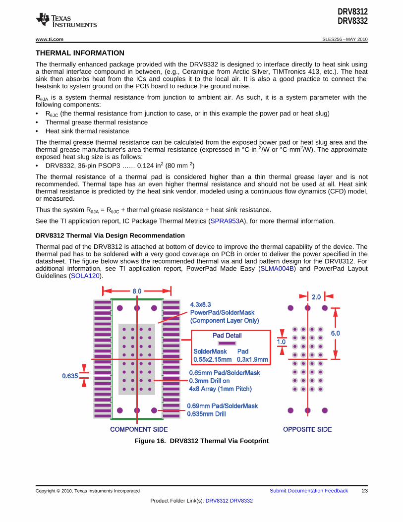
DRV8312 Thermal Via Design Recommendation
Thermal pad of the DRV8312 is attached at bottom of device to improve the thermal capability of the device. Thethermal pad has to be soldered with a very good coverage on PCB in order to deliver the power specified in thedatasheet. The figure below shows the recommended thermal via and land pattern design for the DRV8312. Foradditional information, see TI application report, PowerPad Made Easy (SLMA004B) and PowerPad LayoutGuidelines (SOLA120).
Figure 16. DRV8312 Thermal Via Footprint
Copyright © 2010, Texas Instruments Incorporated Submit Documentation Feedback 23
Product Folder Link(s): DRV8312 DRV8332

PACKAGE OPTION ADDENDUM
www.ti.com 5-Mar-2011
Addendum-Page 1
PACKAGING INFORMATION
Orderable Device Status (1) Package Type PackageDrawing
Pins Package Qty Eco Plan (2) Lead/Ball Finish
MSL Peak Temp (3) Samples
(Requires Login)
DRV8312DDW ACTIVE HTSSOP DDW 44 35 Green (RoHS& no Sb/Br)
CU NIPDAU Level-3-260C-168 HR
DRV8312DDWR ACTIVE HTSSOP DDW 44 2000 Green (RoHS& no Sb/Br)
CU NIPDAU Level-3-260C-168 HR
DRV8332DKD ACTIVE HSSOP DKD 36 29 Green (RoHS& no Sb/Br)
NIPDAU Level-4-260C-72 HR
DRV8332DKDR ACTIVE HSSOP DKD 36 500 Green (RoHS& no Sb/Br)
NIPDAU Level-4-260C-72 HR
(1) The marketing status values are defined as follows:ACTIVE: Product device recommended for new designs.LIFEBUY: TI has announced that the device will be discontinued, and a lifetime-buy period is in effect.NRND: Not recommended for new designs. Device is in production to support existing customers, but TI does not recommend using this part in a new design.PREVIEW: Device has been announced but is not in production. Samples may or may not be available.OBSOLETE: TI has discontinued the production of the device.
(2) Eco Plan - The planned eco-friendly classification: Pb-Free (RoHS), Pb-Free (RoHS Exempt), or Green (RoHS & no Sb/Br) - please check http://www.ti.com/productcontent for the latest availabilityinformation and additional product content details.TBD: The Pb-Free/Green conversion plan has not been defined.Pb-Free (RoHS): TI's terms "Lead-Free" or "Pb-Free" mean semiconductor products that are compatible with the current RoHS requirements for all 6 substances, including the requirement thatlead not exceed 0.1% by weight in homogeneous materials. Where designed to be soldered at high temperatures, TI Pb-Free products are suitable for use in specified lead-free processes.Pb-Free (RoHS Exempt): This component has a RoHS exemption for either 1) lead-based flip-chip solder bumps used between the die and package, or 2) lead-based die adhesive used betweenthe die and leadframe. The component is otherwise considered Pb-Free (RoHS compatible) as defined above.Green (RoHS & no Sb/Br): TI defines "Green" to mean Pb-Free (RoHS compatible), and free of Bromine (Br) and Antimony (Sb) based flame retardants (Br or Sb do not exceed 0.1% by weightin homogeneous material)
(3) MSL, Peak Temp. -- The Moisture Sensitivity Level rating according to the JEDEC industry standard classifications, and peak solder temperature.
Important Information and Disclaimer:The information provided on this page represents TI's knowledge and belief as of the date that it is provided. TI bases its knowledge and belief on informationprovided by third parties, and makes no representation or warranty as to the accuracy of such information. Efforts are underway to better integrate information from third parties. TI has taken andcontinues to take reasonable steps to provide representative and accurate information but may not have conducted destructive testing or chemical analysis on incoming materials and chemicals.TI and TI suppliers consider certain information to be proprietary, and thus CAS numbers and other limited information may not be available for release.
In no event shall TI's liability arising out of such information exceed the total purchase price of the TI part(s) at issue in this document sold by TI to Customer on an annual basis.
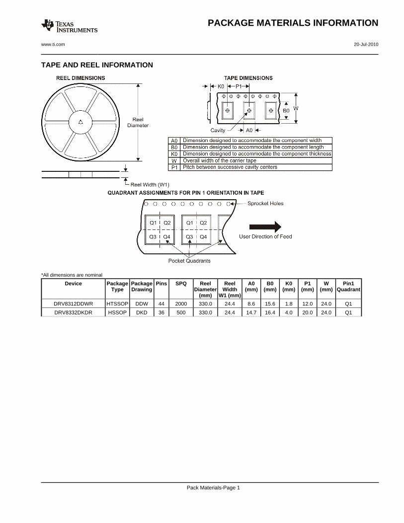
TAPE AND REEL INFORMATION
*All dimensions are nominal
Device PackageType
PackageDrawing
Pins SPQ ReelDiameter
(mm)
ReelWidth
W1 (mm)
A0(mm)
B0(mm)
K0(mm)
P1(mm)
W(mm)
Pin1Quadrant
DRV8312DDWR HTSSOP DDW 44 2000 330.0 24.4 8.6 15.6 1.8 12.0 24.0 Q1
DRV8332DKDR HSSOP DKD 36 500 330.0 24.4 14.7 16.4 4.0 20.0 24.0 Q1
PACKAGE MATERIALS INFORMATION
www.ti.com 20-Jul-2010
Pack Materials-Page 1
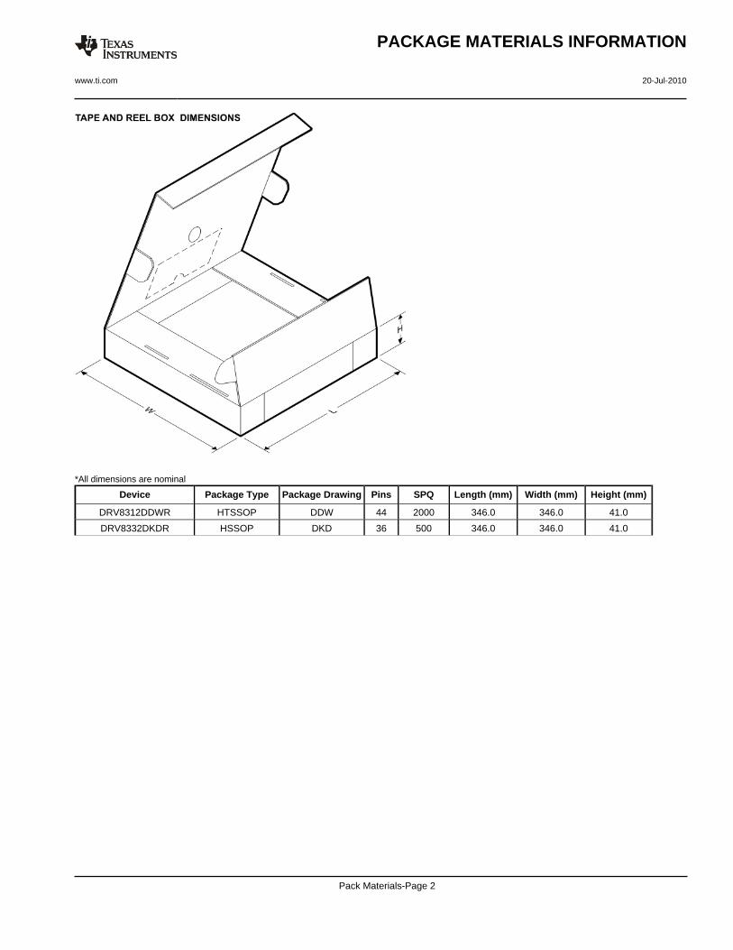
*All dimensions are nominal
Device Package Type Package Drawing Pins SPQ Length (mm) Width (mm) Height (mm)
DRV8312DDWR HTSSOP DDW 44 2000 346.0 346.0 41.0
DRV8332DKDR HSSOP DKD 36 500 346.0 346.0 41.0
PACKAGE MATERIALS INFORMATION
www.ti.com 20-Jul-2010
Pack Materials-Page 2


IMPORTANT NOTICE
Texas Instruments Incorporated and its subsidiaries (TI) reserve the right to make corrections, modifications, enhancements, improvements,and other changes to its products and services at any time and to discontinue any product or service without notice. Customers shouldobtain the latest relevant information before placing orders and should verify that such information is current and complete. All products aresold subject to TI’s terms and conditions of sale supplied at the time of order acknowledgment.
TI warrants performance of its hardware products to the specifications applicable at the time of sale in accordance with TI’s standardwarranty. Testing and other quality control techniques are used to the extent TI deems necessary to support this warranty. Except wheremandated by government requirements, testing of all parameters of each product is not necessarily performed.
TI assumes no liability for applications assistance or customer product design. Customers are responsible for their products andapplications using TI components. To minimize the risks associated with customer products and applications, customers should provideadequate design and operating safeguards.
TI does not warrant or represent that any license, either express or implied, is granted under any TI patent right, copyright, mask work right,or other TI intellectual property right relating to any combination, machine, or process in which TI products or services are used. Informationpublished by TI regarding third-party products or services does not constitute a license from TI to use such products or services or awarranty or endorsement thereof. Use of such information may require a license from a third party under the patents or other intellectualproperty of the third party, or a license from TI under the patents or other intellectual property of TI.
Reproduction of TI information in TI data books or data sheets is permissible only if reproduction is without alteration and is accompaniedby all associated warranties, conditions, limitations, and notices. Reproduction of this information with alteration is an unfair and deceptivebusiness practice. TI is not responsible or liable for such altered documentation. Information of third parties may be subject to additionalrestrictions.
Resale of TI products or services with statements different from or beyond the parameters stated by TI for that product or service voids allexpress and any implied warranties for the associated TI product or service and is an unfair and deceptive business practice. TI is notresponsible or liable for any such statements.
TI products are not authorized for use in safety-critical applications (such as life support) where a failure of the TI product would reasonablybe expected to cause severe personal injury or death, unless officers of the parties have executed an agreement specifically governingsuch use. Buyers represent that they have all necessary expertise in the safety and regulatory ramifications of their applications, andacknowledge and agree that they are solely responsible for all legal, regulatory and safety-related requirements concerning their productsand any use of TI products in such safety-critical applications, notwithstanding any applications-related information or support that may beprovided by TI. Further, Buyers must fully indemnify TI and its representatives against any damages arising out of the use of TI products insuch safety-critical applications.
TI products are neither designed nor intended for use in military/aerospace applications or environments unless the TI products arespecifically designated by TI as military-grade or "enhanced plastic." Only products designated by TI as military-grade meet militaryspecifications. Buyers acknowledge and agree that any such use of TI products which TI has not designated as military-grade is solely atthe Buyer's risk, and that they are solely responsible for compliance with all legal and regulatory requirements in connection with such use.
TI products are neither designed nor intended for use in automotive applications or environments unless the specific TI products aredesignated by TI as compliant with ISO/TS 16949 requirements. Buyers acknowledge and agree that, if they use any non-designatedproducts in automotive applications, TI will not be responsible for any failure to meet such requirements.
Following are URLs where you can obtain information on other Texas Instruments products and application solutions:
Products Applications
Audio www.ti.com/audio Communications and Telecom www.ti.com/communications
Amplifiers amplifier.ti.com Computers and Peripherals www.ti.com/computers
Data Converters dataconverter.ti.com Consumer Electronics www.ti.com/consumer-apps
DLP® Products www.dlp.com Energy and Lighting www.ti.com/energy
DSP dsp.ti.com Industrial www.ti.com/industrial
Clocks and Timers www.ti.com/clocks Medical www.ti.com/medical
Interface interface.ti.com Security www.ti.com/security
Logic logic.ti.com Space, Avionics and Defense www.ti.com/space-avionics-defense
Power Mgmt power.ti.com Transportation and www.ti.com/automotiveAutomotive
Microcontrollers microcontroller.ti.com Video and Imaging www.ti.com/video
RFID www.ti-rfid.com Wireless www.ti.com/wireless-apps
RF/IF and ZigBee® Solutions www.ti.com/lprf
TI E2E Community Home Page e2e.ti.com
Mailing Address: Texas Instruments, Post Office Box 655303, Dallas, Texas 75265Copyright © 2011, Texas Instruments Incorporated
Related Documents