535 W. Research Center Blvd. • Fayetteville, AR 72701 • (479) 443-5759 Three-Dimensional Packaging for Wide Bandgap Based Discrete and Multi-Chip Power Packages www.apei.net Brandon Passmore Sr. Electronics Packaging Research Engineer and Packaging Group Leader [email protected] Brice McPherson, Zach Cole, Peter Killeen, Bret Whitaker, Dan Martin, Adam Barkley, Ty McNutt, Kraig Olejniczak, and Alex Lostetter Applied Power Electronics Conference and Exposition (APEC), March 16 – 20, 2014

Three-Dimensional Packaging for Wide Bandgap Based ... · Group Leader . [email protected]. Brice McPherson, Zach Cole, Peter Killeen, Bret Whitaker, Dan Martin, Adam Barkley, Ty McNutt,
Jul 22, 2020
Welcome message from author
This document is posted to help you gain knowledge. Please leave a comment to let me know what you think about it! Share it to your friends and learn new things together.
Transcript
535 W. Research Center Blvd. • Fayetteville, AR 72701 • (479) 443-5759
Three-Dimensional Packaging for Wide Bandgap Based Discrete and Multi-Chip Power Packages
www.apei.net
Brandon Passmore Sr. Electronics Packaging Research Engineer and Packaging Group Leader [email protected] Brice McPherson, Zach Cole, Peter Killeen, Bret Whitaker, Dan Martin, Adam Barkley, Ty McNutt, Kraig Olejniczak, and Alex Lostetter Applied Power Electronics Conference and Exposition (APEC), March 16 – 20, 2014

www.apei.net
Outline
2
• Company Overview • Motivation of 3D packaging
techniques with wide bandgap power electronics
• Design and performance of X-5 multi-chip power module
• Design and performance of X-6 discrete package
• Summary

www.apei.net
APEI, Inc. Core Technologies
3
Multi-Chip Packaging
High Reliability Modules
Power Circuits & Systems
SiC & GaN Device Expertise
High Density, High Performance Power Electronics
Find us at:

www.apei.net
Motivation for Wide Bandgap Power Electronics
4
High Temperature
Operation
Enabling Capability
High Power Density
Fast Switching;
High Frequency
• Reduce cooling requirements • Reduce system volume/weight • Reduce complexity • Improve performance /reliability
Key Benefits
• High current density • High thermal conductivity substrate
• Reduce size of power filters/capacitors • Reduce size/weight of power system • Allows higher bandwidth for control loops reducing error in AC systems
High temperature multi-layer technologies reduce package size and
increase reliability
3D Packaging Technologies
High current wire bondless
interconnections
Multi-layer packaging technologies reduce
parasitics

www.apei.net
Wide Bandgap Devices Enable Fast Switching Operation
5
• Both GaN and SiC allow High Frequency operation – Reduce switching
losses – Smaller passives – Less expensive cooling
systems • Must Reduce
Package Parasitics to take advantage of WBG characteristics
Integrated Gate Driver
Busboard Reduces Parasitics
Wire Bondless Interconnections


www.apei.net
Design of X-5 Power Module with Integrated Gate Driver
7
Specifications • Full-bridge configuration • 50+ A / 1200 V • 225 °C maximum operation (Tjmax) • 2 MOSFETs / 1 Schottky diode per
switch position • 58 mm × 41 mm × 13 mm (1/3 the
volume of a deck of cards) Package Components • Metal-matrix composite baseplate • AlN DBC Power substrate • High temperature die and power
substrate attach • Integrated busboard enables 3D
Packaging • Integrated gate driver
58 mm
13 mm 41 mm

www.apei.net
X-5 SiC MCPM Junction to Case Thermal Resistance
8
• Experiment ∆Tj-c = 17 °C and Model ∆Tj-c = 15 °C • The experimental and modeled ∆Tj-c are in good agreement • A low junction-to-case thermal resistance of 0.18 °C/W was
measured Experiment Model
Total Pdis = 95.5 W
Spot 136 °C

www.apei.net
0123456
1.E+02 1.E+03 1.E+04 1.E+05 1.E+06
Resi
stan
ce (m
Ω)
Frequency (Hz)
Power Loop Resistance
14
16
18
20
22
1.E+02 1.E+03 1.E+04 1.E+05 1.E+06
Indu
ctan
ce (n
H)
Frequency (Hz)
Power Loop Inductance
Low Parasitic Power Module for High Speed Switching
9
• 3D parasitic model using Comsol Multiphysics® • One side of the full-bridge was analyzed due to the
symmetric design • Inductance/Resistance was modeled vs. frequency
up to 1 MHz • The X-5 exhibited low parasitics at high frequencies • ~4 mΩ and ~16 nH at 500 kHz • Inductance is roughly 1/2 of other commercial power
brick style module [1]
500 kHz
500 kHz
[1] http://www.semikron.com/products/data/cur/assets/SKM100GB12T4_22892020.pdf

www.apei.net
Ultra-Fast Switching From Low Parasitic X-5 / Gate Driver Integration
10
Turn On Waveform
Gate Voltage
Drain Voltage
7.5 ns
• Clamped inductive load • 400 V / 30 A switching waveforms • Rise time = 16.1 ns • Fall time = 7.5 ns • Switching Frequency = 1.2 MHz • Minimal ringing and overshoot
92%
94%
96%
98%
100%
1000 2000 3000 4000 5000 6000
Effic
ienc
y
Output Power [W]
fsw = 250 kHzfsw = 500 kHzfsw = 1 MHzfsw = 1.2 MHz
Boost Converter Efficiency vs. Power

www.apei.net
SiC Charger for Next Generation Toyota Prius Plug-in Hybrid
11
88%
90%
92%
94%
96%
1000 2000 3000 4000 5000 6000
Effic
ienc
y
Output Power
System Efficiency vs. Output Power
System with AC-DC @ 500 kHz
System with AC-DC @ 250 kHz
[2] Toyota, "Plug-in hybrid 2010 model revised (includes 2012 model) emergency response guide," 22 Feb. 2012.
[3] Department of Energy, "EV everywhere: a grand challenge in plug-in electric vehicles, “ 2012.
CHARGER SYSTEM DESIGN TARGETS
Funded by DOE ARPA-e Program
Specifications 2010 Toyota Prius PHEV Charger [2]
Preliminary DOE PHEV On-Board Charger
Targets for 2022 [3]
APEI, Inc. Prototype SiC PHEV Charger
Power Level 2.9 kW 3.3 kW 6.1 kW (Peak) Volume 6.4 L 3.5 L 1.2 L Mass 6.6 kg 3.5 kg 1.6 kg Volumetric power density 0.45 kW/L 0.943 kW/L 5.0 kW/L Gravimetric power density 0.42 kW/kg 0.943 kW/kg 3.8 kW/kg Efficiency 94% >95%
> 10× Power Density
Battery Charger
X-5 Power Module


www.apei.net
Design of X-6 Power Package
13
Specifications • Single die and co-pack • 100+ A / 1200 V • 225 °C maximum operation (Tjmax) • 30 mm × 21 mm × 7 mm Package Features • Compatible with SiC and GaN • Electrically Isolated AlN DBC power substrate • High temperature die and power substrate
attach • High current capable • Low inductance (< 8 nH) • Ultra-fast switching (< 4 ns) • Low Rjc
– 2 mm × 2 mm Die 1.23 °C/W – 5 mm × 5 mm Die 0.5 °C/W
• Modular for system integration • Wire bonded or bondless versions
Wire Bondless Package
Wire Bonded Package
SiC MOSFET X-6 Package

www.apei.net
Wirebondless X-6 Assembly
14
This image cannot currently be displayed.
Housing High temperature plastic) Injection molded
Fasteners Low profile “Captive” in plastic
Interconnects *For wire bondless configurations
PCB, DBC, Thick Film
Contacts
Base Plate
Substrate
Panelized & Etched
DBC, DBA, AMB, etc.
Copper or MMC


www.apei.net
X-6 Package Junction to Case Thermal Resistance
16
• Experimental Rj-c = 1.23 °C/W • Modeled Rj-c = 1.15 °C/W • The experimental and modeled
Rj-c are in good agreement • ~ 50 % of the thermal
resistance of the package is in the AlN layer of the DBC
• Rj-c can be reduced further using DBC with a thinner AlN layer
Experiment
Model
Pdis = 48 W
Pdis = 48 W
Spot = 66 °C

www.apei.net
X-6 Parasitic Modeling
17
FLIP CHIP Dual Substrate
WIRE BOND LOOPS WIRE BOND LOOPS
X-6 Package TO-254 Package
PIN LENGTH
Wire Bonded SiC TMOS Wire Bondless GaN HEMT TO-254 – SiC TMOS

www.apei.net
Discrete Package Resistance Comparison
18
GaN HEMT SiC TMOS TO-254 0 >4
A/mm2
Current Density
Power Loop
0 >4 A/mm2
Current Density
Gate Loop

www.apei.net
Discrete Package Inductance Comparison
19
GaN HEMT SiC TMOS TO-254
Wire Bonded SiC TMOS
Wire Bondless GaN HEMT
TO-254 – SiC TMOS

www.apei.net
High Efficiency GaN HEMT Boost Convertor
20
• 200 - 300 V Input / 400 V Output • Switching Frequency = 100 kHz • Turn on ~ 8.2 ns, Turn off ~ 3.7 ns • Minimal Ringing • Up to 5 kW • > 99 % Peak Efficiency @ 100 kHz • 97.5 % @ 1 MHz
3.72 ns
www.apei.net
Summary
21
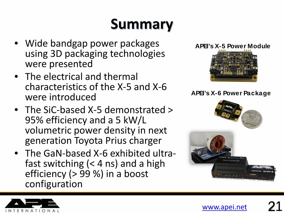
• Wide bandgap power packages using 3D packaging technologies were presented
• The electrical and thermal characteristics of the X-5 and X-6 were introduced
• The SiC-based X-5 demonstrated > 95% efficiency and a 5 kW/L volumetric power density in next generation Toyota Prius charger
• The GaN-based X-6 exhibited ultra-fast switching (< 4 ns) and a high efficiency (> 99 %) in a boost configuration
APEI’s X-5 Power Module
APEI’s X-6 Power Package

www.apei.net
Connect With Us!
22
• Half-bridge +300 A / 1200 V • Standard power module footprint • Device neutral • 225 °C maximum operation (Tjmax) • Minimized parasitics (< 7 nH) • Low thermal resistance (< 0.1 °C/W) • Low volume/weight (72 cm3 and 140 g)
Wide Bandgap HT-3000 Power Module
Related Documents
![Killeen, Thomas B. TOCs/Killeen, Thomas B.toc.pdf · 2012-12-17 · 2 INTERVIEW [Note: This transcript was not edited by Mr. Killeen.] SUMMARY: This history of Thomas B. Killeen focuses](https://static.cupdf.com/doc/110x72/5fba91d984c64d2537799e12/killeen-thomas-b-tocskilleen-thomas-btocpdf-2012-12-17-2-interview-note.jpg)