Journal of Microscopy, Vol. 248, Pt 2 2012, pp. 129–139 doi: 10.1111/j.1365-2818.2012.03656.x Received 20 April 2012; accepted 17 July 2012 Three-dimensional nanofabrication of polystyrene by focused ion beam C.C. LEE ∗ , G. PROUST †, G. ALICI ‡, G.M. SPINKS ‡ & J.M. CAIRNEY ∗ ∗ Australian Centre for Microscopy & Microanalysis, University of Sydney, Australia †School of Civil Engineering, University of Sydney, Australia ‡School of Mechanical, Materials & Mechatronic Engineering, University of Wollongong, Australia Key words. Beam damage, focused ion beam, low temperature milling, microcantilever, polystyrene. Summary Focused ion beam micromachining provides a maskless and resistless technique for prototyping of structures from thermoplastic polymers, an example being the production of polystyrene microcantilevers with potential applications as micro/nanoelectromechanical systems sensors and actuators. The applicability of FIB technology is, however, often restricted by the damage created by high energy gallium ion bombardment and local beam heating, which can affect the desired properties and limit the minimum achievable size of the fabricated structure. To investigate the ion-induced damage and determine the limitations of the technique for polymer nanofabrication, we have exposed thin polystyrene film to the ion beam at varying ion doses, ion energies and specimen temperatures. Ion doses ranging from 10 16 to 10 18 ions cm −2 show significant gallium implantation, redeposition of sputtered material and chemical degradation in the polymer. Raman results show that the local heating in polymer during milling is severe at room temperature, damaging the aromatic carbon bonding (C = C) in particular. These observations are supported by the results of a beam heating model and Monte Carlo simulations. The chemical degradation caused by local beam heating is found to be significantly reduced by cooling the specimen to −25 ◦ C during milling. This is consistent with observations that reversible and repeatable thermal actuation of a fabricated polystyrene–platinum microcantilever is only observed when the cantilever is prepared at low temperature milling. Using this cooling approach, polymer structures can be fabricated with dimensions as low as 200 nm and still retain a sufficient volume of material unaffected by the ion beam. Correspondence to: J.M. Cairney, Australian Centre for Microscopy & Microanalysis, Madsen Building F09, University of Sydney, NSW 2006 Australia. Tel: +61-2-9351- 4523; fax: +61-2-9351-7682; e-mail: [email protected] Introduction Focused ion beam (FIB) is a maskless technology that can be used for machining and depositing a wide range of materials with nanometre-scale precision. It has proven to be an invaluable tool for micro/nanofabrication prototyping (Prewett, 1993; Wilhelmi et al., 2008), microscopy specimen preparation (Giannuzzi & Stevie, 1999; Saxey et al., 2007; Felfer et al., 2012), materials characterization (Cairney et al., 2000), device modification (Walker et al., 1996) and ion lithography (Tseng, 2005). Most FIB applications to-date have been on metals and semiconductors, and its use on soft materials like polymers and biological samples is an emerging area. These soft materials are highly susceptible to ion irradiation, and may even lead to an overall change of the materials’ properties in the fabricated structure. Understanding and limiting ion-induced damage is, therefore, very important when applying FIB technology to polymers. FIB technology has many applications that are particularly useful for polymers, such as surface modification to improve wettability, adhesion properties and biocompatibility (Abeysinghe et al., 2009); site-specific specimen preparation for electron microscopy (Loos et al., 2002); as well as production of micro/nanometre-scale devices (Lee et al., 2011). The authors have recently been using this technique for the production of free-standing polystyrene–platinum bimorph cantilever thermal microactuators for MEMS/NEMS applications (Lee et al., 2011). These applications may, however, be limited by the creation of unwanted morphological and chemical modifications in the polymers due to variations in the surface structure of the polymer film (Ektessabi & Sano, 2000; Niihara et al., 2005; Sezen et al., 2009; Kim et al., 2011; Sezen et al., 2011). Critical issues in polymer micro/nanofabrication using the ion beam include direct sputtering and indirect thermal evaporation of surface atoms/molecules, depletion of main components C 2012 The Authors Journal of Microscopy C 2012 Royal Microscopical Society

Welcome message from author
This document is posted to help you gain knowledge. Please leave a comment to let me know what you think about it! Share it to your friends and learn new things together.
Transcript
Journal of Microscopy, Vol. 248, Pt 2 2012, pp. 129–139 doi: 10.1111/j.1365-2818.2012.03656.x
Received 20 April 2012; accepted 17 July 2012
Three-dimensional nanofabrication of polystyrene by focusedion beam
C . C . L E E ∗, G . P R O U S T†, G . A L I C I‡, G . M . S P I N K S‡& J . M . C A I R N E Y ∗∗Australian Centre for Microscopy & Microanalysis, University of Sydney, Australia†School of Civil Engineering, University of Sydney, Australia
‡School of Mechanical, Materials & Mechatronic Engineering, University of Wollongong, Australia
Key words. Beam damage, focused ion beam, low temperature milling,microcantilever, polystyrene.
Summary
Focused ion beam micromachining provides a masklessand resistless technique for prototyping of structures fromthermoplastic polymers, an example being the production ofpolystyrene microcantilevers with potential applications asmicro/nanoelectromechanical systems sensors and actuators.The applicability of FIB technology is, however, oftenrestricted by the damage created by high energy galliumion bombardment and local beam heating, which can affectthe desired properties and limit the minimum achievable sizeof the fabricated structure. To investigate the ion-induceddamage and determine the limitations of the technique forpolymer nanofabrication, we have exposed thin polystyrenefilm to the ion beam at varying ion doses, ion energiesand specimen temperatures. Ion doses ranging from 1016
to 1018 ions cm−2 show significant gallium implantation,redeposition of sputtered material and chemical degradationin the polymer. Raman results show that the local heatingin polymer during milling is severe at room temperature,damaging the aromatic carbon bonding (C = C) in particular.These observations are supported by the results of a beamheating model and Monte Carlo simulations. The chemicaldegradation caused by local beam heating is found to besignificantly reduced by cooling the specimen to −25◦Cduring milling. This is consistent with observations thatreversible and repeatable thermal actuation of a fabricatedpolystyrene–platinum microcantilever is only observed whenthe cantilever is prepared at low temperature milling. Usingthis cooling approach, polymer structures can be fabricatedwith dimensions as low as 200 nm and still retain a sufficientvolume of material unaffected by the ion beam.
Correspondence to: J.M. Cairney, Australian Centre for Microscopy & Microanalysis,
Madsen Building F09, University of Sydney, NSW 2006 Australia. Tel:+61-2-9351-
4523; fax: +61-2-9351-7682; e-mail: [email protected]
Introduction
Focused ion beam (FIB) is a maskless technology that canbe used for machining and depositing a wide range ofmaterials with nanometre-scale precision. It has proven tobe an invaluable tool for micro/nanofabrication prototyping(Prewett, 1993; Wilhelmi et al., 2008), microscopy specimenpreparation (Giannuzzi & Stevie, 1999; Saxey et al., 2007;Felfer et al., 2012), materials characterization (Cairney et al.,2000), device modification (Walker et al., 1996) and ionlithography (Tseng, 2005). Most FIB applications to-datehave been on metals and semiconductors, and its use onsoft materials like polymers and biological samples is anemerging area. These soft materials are highly susceptibleto ion irradiation, and may even lead to an overall changeof the materials’ properties in the fabricated structure.Understanding and limiting ion-induced damage is, therefore,very important when applying FIB technology to polymers.
FIB technology has many applications that are particularlyuseful for polymers, such as surface modification toimprove wettability, adhesion properties and biocompatibility(Abeysinghe et al., 2009); site-specific specimen preparationfor electron microscopy (Loos et al., 2002); as well asproduction of micro/nanometre-scale devices (Lee et al.,2011). The authors have recently been using this techniquefor the production of free-standing polystyrene–platinumbimorph cantilever thermal microactuators for MEMS/NEMSapplications (Lee et al., 2011). These applications may,however, be limited by the creation of unwantedmorphological and chemical modifications in the polymersdue to variations in the surface structure of the polymerfilm (Ektessabi & Sano, 2000; Niihara et al., 2005; Sezenet al., 2009; Kim et al., 2011; Sezen et al., 2011). Criticalissues in polymer micro/nanofabrication using the ion beaminclude direct sputtering and indirect thermal evaporationof surface atoms/molecules, depletion of main components
C© 2012 The AuthorsJournal of Microscopy C© 2012 Royal Microscopical Society

1 3 0 C . C . L E E E T A L .
of the polymer such as carbon, hydrogen, oxygen, etc.,rearrangement of chemical bonds and cross-linking, andincorporation of ions into the film (Ektessabi & Sano, 2000).All of these changes, which are expected to be limited to thesurface region that is exposed to the ion beam, may degradethe properties and limit the minimum achievable size of thefabricated structure.
Both direct physical sputtering and indirect heat-inducedphenomena are responsible for the removal of polymersusing the ion beam (Volkert & Minor, 2007). The ion-polymer interaction results in bond cleavage, chain scission,evaporation of monomer and other molecular fragments,followed by secondary processes such as phonon productionand transport, which lead to heat generation. The dose inions cm−2 can be calculated according to Eq. (1) for an ioncurrent (Iion) of gallium source in pA, exposure time (tmill) ins, and pattern area (Apattern) in μm2 (Huey & Langford, 2003)
D ose = Iion x tmill
Apattern x 1.602x10⁻¹⁵(1)
The local temperature rise under the ion beam can beestimated by using a beam heating model (Melngailis, 1987;Volkert & Minor, 2007)
�T = Pπaκ
(2)
where P is the power of the ion beam, a is the radius ofthe circular ion beam profile on the specimen surface andκ is the thermal conductivity of the specimen. Due to theirlow thermal conductivity, the temperature rise for typicalpolymers can be thousands of times higher than that ofmetals and semiconductors. Possible routes to minimize thedamage caused by the ion beam include milling the polymers atcryogenic temperatures (e.g. −150◦C) to reduce local heating(Niihara et al., 2005; Sezen et al., 2009; Kim et al., 2011; Sezenet al., 2011), applying an electrically conductive coating orusing an electron flood gun against ion charging (Stokes et al.,2007) or removing the polymer at a faster rate using watervapour (Kochumalayil et al., 2009a, b).
In this paper, we investigate alternative methods to limit theion-induced damage in polystyrene and provide an estimationof the minimum achievable size of FIB-fabricated polystyrene-based structures that will still retain a sufficient volume ofmaterial unaffected by the ion beam. We investigate thestructural and chemical modification in the polystyrene thinfilm depending on the ion dose, ion energy and specimentemperature. The surface morphology, composition andchemistry of the milled regions are systematically studiedusing scanning electron microscopy (SEM), energy dispersivex-ray spectroscopy (EDS) and Raman spectroscopy.
Methodology
For the polymer film preparation, a drop of polystyrene(Mw 45 000) solution prepared in chloroform is first cast
onto the surface of a cleaned glass slide while being rotatedat 7000 rpm for 120 s. The film is then annealed on ahot plate for 2 h at 75◦C. The film is peeled from the glasssubstrate using a razor blade and mounted onto an aluminiumstub using carbon adhesive tape. The film is then sputter-coated with a layer of platinum (thickness of ∼30 nm) toprevent charging during ion/electron beam exposure. Thethickness of the polystyrene film, measured using SEM, isapproximately 5 μm.
The suspended polystyrene film is exposed to focusedgallium ions at an energy of 30 keV (unless stated otherwise)and currents ranging from 10 to 1000 pA at room temperatureand −25◦C in a dual-beam FIB-SEM workstation (FEIQuanta 200), equipped with a Peltier stage (Caron 2050W).Rectangular patterns of dimensions 5 μm long × 5 μm wideare milled onto the polymer surface by scanning the ion beamover the area in a serpentine pattern for a period of 1–10 min ata normal incidence angle with a beam dwell time and overlapof 100 ns and 50%, respectively. A constant beam overlap isused for a general comparison, although it should be notedthat the actual point pitch is affected by the beam diameter atdifferent beam currents (6 nm for 10 pA, 12 nm for 100 pAand 25 nm for 1000 pA).
The surface morphology is studied using a field emissionSEM (Zeiss UltraPlus). The milled depth of the rectangulartrenches was measured from the SEM images taken atan oblique view (45◦) and converted into real distance.The compositional analysis is obtained using an EDSsystem (Oxford Instruments & Intellection Qemscan), which isincorporated to the SEM. The EDS data is acquired with 2and 5 keV electron beam. The chemistry is probed using aRaman spectrometer (Renishaw inVia), coupled to an opticalmicroscope, with excitation from the 514 nm line of an argonion (Ar+) laser operating at an incident power of 25 mW anda total exposure time of 10 s. The laser power is attenuatedto 50% to avoid burning a hole into the thin polystyrene film.Both EDS and Raman measurements were carried out withpoint analysis (average of at least 2 spectra) at the centre ofthe bottom-wall of the milled trench.
To fabricate polystyrene–platinum bimorph microcanti-levers, a combination of FIB capabilities (i.e. deposition, millingand lift-out) were performed. A platinum strip is first depositedonto the polymer surface using an ion beam voltage of 30 kV,beam current of 30 pA, beam dwell time of 200 ns and beamoverlap of 0%. Then, a series of milling steps is executed inthe vicinity of the platinum strip using a beam voltage of 30kV, beam current of 500 pA, beam dwell time of 100 ns andbeam overlap of 50% to form a bridge cantilevered structure.The cantilever is then cut free from the bulk specimen. Finally,the cantilever is transferred to the desired support structureusing a tungsten microprobe. This procedure is described indetail elsewhere (Lee et al., 2011). In this study, the bimorphmicrocantilevers were fabricated with FIB milling at roomtemperature and −25◦C.
C© 2012 The AuthorsJournal of Microscopy C© 2012 Royal Microscopical Society, 248, 129–139
N A N O F A B R I C A T I O N O F P O L Y S T Y R E N E B Y F I B 1 3 1
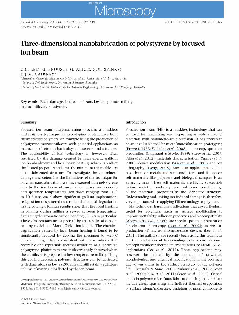
Fig. 1. SEM images of rectangular patterns milled at (a–c) different beam currents with a fixed exposure time of 5 min which corresponds to differention doses and (d–e) different combinations of beam currents and exposure times which corresponds to identical ion doses. Images are taken with thespecimen tilted at an angle of 45◦ from the electron beam path to provide some perspective on the milling depth.
Results & discussion
SEM images of the polystyrene film with rectangular patternsmilled using beam currents ranging from 10 to 1000 pA for5 min (the corresponding ion dose ranges from 7.5 × 10¹⁶ to7.5 × 1018 ions cm−2) at room temperature are shownin Figure 1(a)–(c). Before milling, the polystyrene film(which is coated with a platinum layer to prevent charging)has a smooth, featureless surface morphology. After ionbombardment, some polystyrene was removed from the milledregions, but there was no discernible change in the surfacemorphology. The milled areas are clearly visible as rectangularfeatures in the SEM micrographs. Outside the milled patterns,the polymer surface is still covered with the platinum coating.However, at higher beam currents, some milling outside thedefined rectangular area also occurs due to an extendedGaussian beam tail profile (or local beam heating; Yao, 2007).
As expected, a lower beam current (corresponding to a lowerion dose with a fixed exposure time) was found to be slower tomill away the polymer as the milling rate is primarily governedby the beam current and exposure time (or dwell time; Yao,2007). The depth of milling is minimal for doses of 1016
ions cm−2 and less, extends to several hundreds nanometresfor doses of 1017 ions cm−2 and reaches several micrometresfor doses above 1018 ions cm−2. A discrepancy in ion doseof about two orders of magnitude (the corresponding beamcurrents of 10 and 1000 pA) resulted in a difference in themilled depth of approximately 30 times.
At relatively high ion doses (>1018 ions cm−2, whichcorresponds to beam currents above 1000 pA), the side-walland bottom-wall of the rectangular milled trenches were foundto be uneven. The incline of the side-wall and the unevensurface of the bottom-wall were observed under the influenceof redeposition. The atoms sputtered from the bottom of themilled region can be redeposited onto the side-wall and/orvice-versa, especially in deep cross-sections where the milleddepth is almost unity compared to the width of the trench.Significant redeposition is unlikely, however, for doses lowerthan 1016 ions cm−2 as the surface is not appreciably milled.The amount of redeposition is dependent on the geometryof the patterns, the dynamics of the sputtered atoms and thesticking coefficient of the target materials as well as the millingconditions such as ion energy, ion current, exposure time andnumber of scan passes. Redeposition is prone to occur at higheraspect ratio, higher ion energy and current as well as longerexposure time (or dwell time) and reduced scan passes (Yao,2007).
Figure 1(d)–(e) shows SEM images of the polystyrene filmwith rectangular patterns milled at room temperature usingdifferent beam currents (100 and 1000 pA) but the ion dosesare kept constant (1.5 × 10¹⁸ ions cm−2). This corresponds toexposure times of 10 min for the region milled at 100 pAand 1 min for the area milled at 1000 pA. Despite thesimilarity in ion doses, the milled depths are not equal.
C© 2012 The AuthorsJournal of Microscopy C© 2012 Royal Microscopical Society, 248, 129–139
1 3 2 C . C . L E E E T A L .
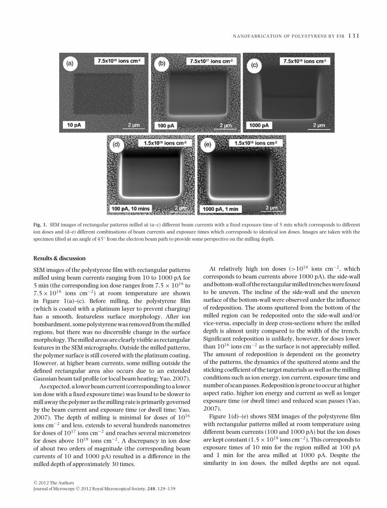
Fig. 2. SEM images of rectangular patterns milled at a fixed ion dose with (a–c) different beam voltages (beam currents of ∼100 pA and exposure timesof 5 min) and (d–e) different specimen temperatures (beam currents of 1000 pA and exposure time of 5 min). Images are taken with the specimen tiltedat an angle of 45◦ from the electron beam path to provide some perspective on the milling depth. RT signifies room temperature.
The rectangular pattern milled using 100 pA has a deepertrench (approximately twice the milled depth) than that milledusing 1000 pA. Although having identical ion doses basedon Eq. (1), the effect of sputtering and redeposition may bedifferent when milling using different beam currents. Forinstance, the vicinity of the trench milled at 1000 pA is affectedby the extended beam tail profile (or local beam heating), andthis can have an effect on the depth of milling. The beamcurrent is known to dictate the damage rate of a cut featureand the amount of time required to mill a selected volume (Yao,2007). The beam current and beam exposure time should beproperly selected to ensure that each milled pattern cuts to thedesired depth.
Figure 2(a)–(c) shows SEM images of the polystyrene filmwith patterns milled at room temperature using beam voltagesranging from 10 to 30 kV (this corresponds to similar ion doseswith beam currents of ∼100 pA and beam exposure time of5 min). There is no large disparity in terms of milled depth,given the fact that the beam currents and beam exposuretimes are similar in all cases. This implies that the milling rate,and therefore the milled depth is strongly affected by the beamcurrent and exposure time, but much less strongly affected bythe beam voltage, consistent with the observations of others(Kolibal et al., 2011). Although it has little effect on the millingrate, the beam voltage can be used to control the depth ofdamage caused by ion implantation (Yao, 2007; Felfer et al.,2011). The effect of beam voltage on gallium implantationin polystyrene will be discussed in the EDS and simulationsections.
Rectangular trenches milled at room temperature and−25◦C using identical ion doses (this corresponds to beamcurrent of 1000 pA at the exposure time of 5 min) were foundto have comparable depths, as shown in the SEM images inFigure 2(d)–(e). There was some variation from the expectedrectangular patterns in both cases, which is attributed todrift from charging due to depletion of the platinum coatingat high beam currents. As previously stated, redepositionoccurs when milling using a higher beam current (increasein the milling rate). The bottom-wall and side-wall of thetrenches were found to be uneven, particularly in the caseof low temperature milling (Kim et al., 2011). The specimentemperature used here (−25◦C) provides an alternativeto the typical cryogenic temperatures, which often causesevere specimen drift and require a complicated experimentalsetup (Kim et al., 2011). The effect of low temperaturemilling on the chemical structure of the polystyrene will bediscussed later with reference to the results of the Ramananalysis.
EDS is used to give a qualitative indication of the amountof gallium implanted into the polymer. The results canonly be relative rather than absolute due to the interactionvolume of the 5 keV electron beam being different to theion penetration depth. For this reason, EDS analysis has beencarried out using two different electron beam voltages: 5 and2 kV. The penetration of the 2 keV electron beam is muchsmaller (∼125 nm) than that of the 5 keV electron beam(∼550 nm), as predicted by Monte Carlo simulations (CASINOsoftware program). The 2 keV measurements are, therefore,
C© 2012 The AuthorsJournal of Microscopy C© 2012 Royal Microscopical Society, 248, 129–139
N A N O F A B R I C A T I O N O F P O L Y S T Y R E N E B Y F I B 1 3 3
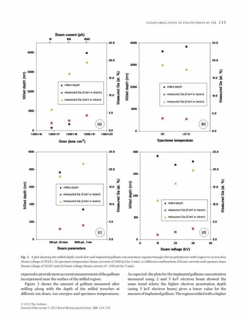
Fig. 3. A plot showing the milled depth (circle dot) and implanted gallium concentration (square/triangle dot) in polystyrene with respect to (a) ion dose(beam voltage of 30 kV), (b) specimen temperature (beam currents of 1000 pA for 5 min), (c) different combinations of beam currents and exposure times(beam voltage of 30 kV) and (d) beam voltage (beam current of ∼100 pA for 5 min).
expected to provide more accurate measurement of the galliumincorporated near the surface of the milled region.
Figure 3 shows the amount of gallium measured aftermilling along with the depth of the milled trenches atdifferent ion doses, ion energies and specimen temperatures.
As expected, the plots for the implanted gallium concentrationmeasured using 2 and 5 keV electron beam showed thesame trend where the higher electron penetration depth(using 5 keV electron beam) gives a lower value for theamount of implanted gallium. The regions milled with a higher
C© 2012 The AuthorsJournal of Microscopy C© 2012 Royal Microscopical Society, 248, 129–139
1 3 4 C . C . L E E E T A L .
beam current (1000 pA), and therefore, a higher ion dose,contain the most gallium (see Fig. 3a). A rise in the galliumconcentration may also be due to redeposition of the sputteredmaterial at the bottom-wall of the milled trench (Rubanov &Munroe, 2004).
The side-wall of a deeper milled trench is also likely toinfluence the amount of measured gallium. To confirm this, alarger pattern (10 μm × 10 μm) was milled using the sameion dose as the 5 μm × 5 μm milled trench (the same beamcurrent of 1000 pA at the exposure time of 20 min). The resultsshowed a lower gallium concentration (about 50%) comparedto that measured for the 5 μm × 5 μm milled trench.
For a fixed ion dose, the gallium concentration measured inthe regions milled at different specimen temperatures showedinsignificant disparity, thus indicating that low temperaturemilling neither eliminates nor reduces the gallium ions fromthe polymer matrix (see Fig. 3b). However, for differentcombinations of beam currents and exposure times, thegallium concentration is higher in the trench milled usinga higher beam current (see Fig. 3c). This is thought to becaused by redeposition at the bottom-wall of the milled regionusing a beam current of 1000 pA. The actual milling depthis, therefore, lesser than the nominal value owing to theredeposited layer at the bottom-wall of the milled trench.
For trenches milled at different beam voltages, the galliumconcentration was found to increase with increasing beamvoltage (see Fig. 3d), despite having comparable ion dose andmilled depth. The gallium concentration increased by a factorof 2 when the beam voltage was increased from 10 to 30 kV.It is well established that the depth of gallium implantationis related to the energy of the incident gallium ion (Nastasiet al., 1996). Given that the damage region could not bedirectly observed from the SEM images, the depth of galliumimplantation for different beam voltages can be estimatedusing Monte Carlo simulations, which will be discussed inthe following section.
A TRansport of Ions in Matter/Stopping Range of Ions inMatter (TRIM/SRIM) software package (http://www.srim.org;Ziegler & Manoyan, 1988) was used to estimate the stoppingrange of ions, the range where recoil atoms appear and thedamage distribution with respect to the ion energy and ionincidence angle. Figure 4(a) shows simulated results for 30keV gallium ions (1000 ions) implanted into polystyrene. Thecollision cascade due to ion implantation (red trajectories) andrecoil carbon and hydrogen atoms (blue/green trajectories)extend to about 100 nm deep into the polymer. Although theaffected region of the recoil atoms is larger than that ofthe penetrating ions, the target depths (penetration depth forthe ions or influence depth for the recoil atoms) are similar.
Figure 4(b) shows simulated results for the same ionsimplanted into pure platinum, for which the projected rangeis much lower at 30 nm. The damage created in metals iscontained within the near-surface region whereas the ionspenetrate much deeper into the polymers, resulting in a larger
interaction volume and, therefore, creating considerablechemical degradation. The ion implantation is known toinduce cross-linking or create new chemical groups in thepolymer (Ektessabi & Sano, 2000).
Damage can also be expected from the recoil atoms,produced when atoms within the specimen receive energythat exceeds their displacement energies. Recoil atoms cangenerate defects which lead to redeposition, amorphizationand/or recrystallization, as has been observed in hardmaterials like metals and semiconductors (Rubanov &Munroe, 2004). In polymers, the recoil atoms can furtherresult in chain scissioning, which causes permanent chemicaldamage that may even extend wider and deeper into thepolymer. The TRIM/SRIM simulations indicated that thedamage in polymer samples can be limited by controllingthe FIB milling conditions, particularly the ion energy. Thedepth of the damaged surface region can be reduced by usinga lower beam voltage.
Figure 4(c)–(d) shows simulated results for 20 and 10keV gallium ions (1000 ions) implanted into polystyrene,respectively. The projected ranges are approximately 50%lower than for 30 keV gallium ions implanted under the samebeam conditions (a damage depth of ∼50 nm compared to∼100 nm). This is consistent with the EDS results, in whichthe gallium concentration increases with the increasing beamvoltage. A low beam voltage obviously creates less damage.However, it does impose restrictions on the achievable three-dimensional prototypes. The minimum achievable feature sizeand the maximum aspect ratio are limited at low voltage dueto a reduction in the resolution of the ion beam.
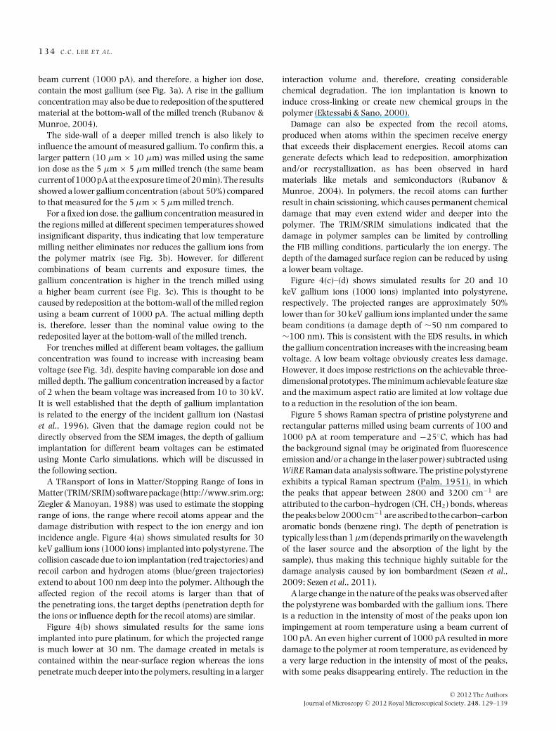
Figure 5 shows Raman spectra of pristine polystyrene andrectangular patterns milled using beam currents of 100 and1000 pA at room temperature and −25◦C, which has hadthe background signal (may be originated from fluorescenceemission and/or a change in the laser power) subtracted usingWiRE Raman data analysis software. The pristine polystyreneexhibits a typical Raman spectrum (Palm, 1951), in whichthe peaks that appear between 2800 and 3200 cm−1 areattributed to the carbon–hydrogen (CH, CH2) bonds, whereasthe peaks below 2000 cm−1 are ascribed to the carbon–carbonaromatic bonds (benzene ring). The depth of penetration istypically less than 1 μm (depends primarily on the wavelengthof the laser source and the absorption of the light by thesample), thus making this technique highly suitable for thedamage analysis caused by ion bombardment (Sezen et al.,2009; Sezen et al., 2011).
A large change in the nature of the peaks was observed afterthe polystyrene was bombarded with the gallium ions. Thereis a reduction in the intensity of most of the peaks upon ionimpingement at room temperature using a beam current of100 pA. An even higher current of 1000 pA resulted in moredamage to the polymer at room temperature, as evidenced bya very large reduction in the intensity of most of the peaks,with some peaks disappearing entirely. The reduction in the
C© 2012 The AuthorsJournal of Microscopy C© 2012 Royal Microscopical Society, 248, 129–139

N A N O F A B R I C A T I O N O F P O L Y S T Y R E N E B Y F I B 1 3 5
Fig. 4. (colour Online). SRIM plots of 1000 gallium ions sputtered into polystyrene and platinum at different beam voltages: (a) 30 keV ions in polystyrene,(b) 30 keV ions in platinum, (c) 20 keV ions in polystyrene and (d) 10 keV ions in polystyrene. Red path is ion implantation trajectories and green andblue paths are recoil atoms trajectories.
intensity of the peaks occurred for all bond types (carbon–carbon and carbon–hydrogen). A reduction and broadeningin the appearance of the peak corresponding specifically to theC = C bond, labelled in Figure 5, indicates major destructionto the ring structure, resulting in loss of conjugation. Thescission of the carbon–carbon bonds produces volatile chainfragments that are easily evaporated from the polymer surface.The changes in the carbon bonding strongly influence thechemical state of the polymer.
Comparatively, the Raman spectrum obtained for the regionmilled using a beam current of 1000 pA at −25◦C has a muchbetter resemblance to the pristine polystyrene. This suggeststhat milling at room temperature using a high beam currentcan produce sufficient local heating to result in substantialdegradation to the polymer structure than the one milled atthe same beam current at −25◦C. The chemical degradationin polystyrene is strongly driven by local beam heating, wherethe heat generated in the polymer upon ion bombardment
leads to massive bond cleavage and chain scission. Cooling to−25◦C has shown significant improvement for retaining thestructure of the polymer under higher ion dose (correspondsto a high beam current). It is also, therefore, not necessary touse cryogenic temperatures for such process.
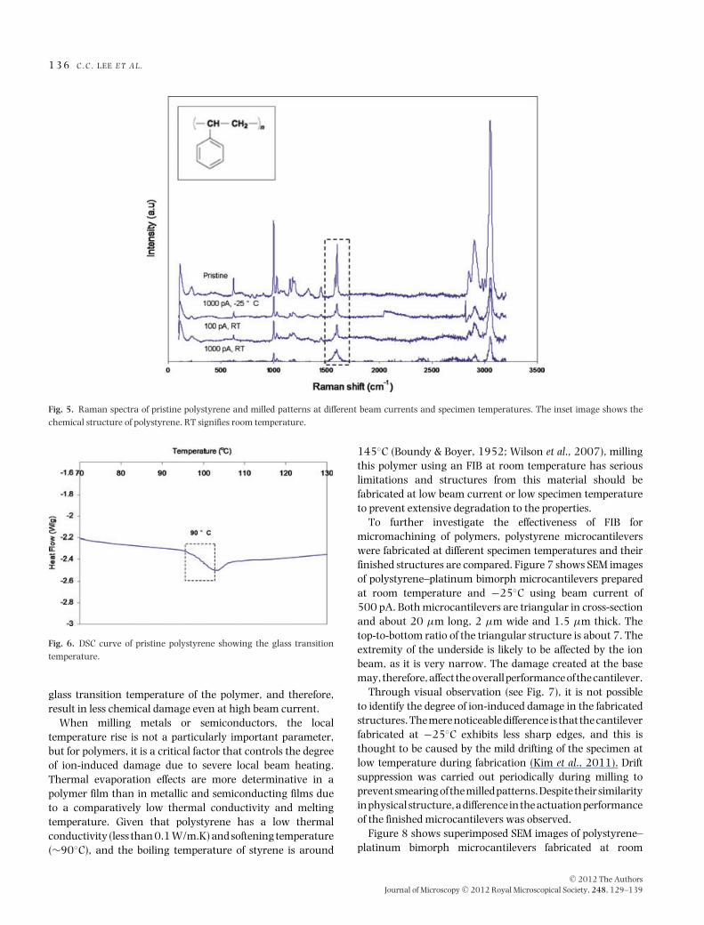
At room temperature, the local temperature rise withinand around the affected region was estimated (by usingEq. (2)) to be about 120◦C for polystyrene under ourexperimental conditions. Polystyrene usually exhibits a glasstransition temperature of ∼90–100◦C, and this has beendirectly measured for our spin-cast polystyrene film by usingdifferential scanning calorimetry (DSC; see Fig. 6). Surfaceheating to 120◦C would, therefore, result in local softening,instead of milling in the vicinity of the intended feature,which leads to severe chemical degradation and considerablyaffects the thermomechanical properties of the polymer. It isreasonable to expect that cooling the specimen during millingwould lower the local temperature, quite possibly below the
C© 2012 The AuthorsJournal of Microscopy C© 2012 Royal Microscopical Society, 248, 129–139
1 3 6 C . C . L E E E T A L .
Fig. 5. Raman spectra of pristine polystyrene and milled patterns at different beam currents and specimen temperatures. The inset image shows thechemical structure of polystyrene. RT signifies room temperature.
Fig. 6. DSC curve of pristine polystyrene showing the glass transitiontemperature.
glass transition temperature of the polymer, and therefore,result in less chemical damage even at high beam current.
When milling metals or semiconductors, the localtemperature rise is not a particularly important parameter,but for polymers, it is a critical factor that controls the degreeof ion-induced damage due to severe local beam heating.Thermal evaporation effects are more determinative in apolymer film than in metallic and semiconducting films dueto a comparatively low thermal conductivity and meltingtemperature. Given that polystyrene has a low thermalconductivity (less than 0.1 W/m.K) and softening temperature(∼90◦C), and the boiling temperature of styrene is around
145◦C (Boundy & Boyer, 1952; Wilson et al., 2007), millingthis polymer using an FIB at room temperature has seriouslimitations and structures from this material should befabricated at low beam current or low specimen temperatureto prevent extensive degradation to the properties.
To further investigate the effectiveness of FIB formicromachining of polymers, polystyrene microcantileverswere fabricated at different specimen temperatures and theirfinished structures are compared. Figure 7 shows SEM imagesof polystyrene–platinum bimorph microcantilevers preparedat room temperature and −25◦C using beam current of500 pA. Both microcantilevers are triangular in cross-sectionand about 20 μm long, 2 μm wide and 1.5 μm thick. Thetop-to-bottom ratio of the triangular structure is about 7. Theextremity of the underside is likely to be affected by the ionbeam, as it is very narrow. The damage created at the basemay, therefore, affect the overall performance of the cantilever.
Through visual observation (see Fig. 7), it is not possibleto identify the degree of ion-induced damage in the fabricatedstructures. The mere noticeable difference is that the cantileverfabricated at −25◦C exhibits less sharp edges, and this isthought to be caused by the mild drifting of the specimen atlow temperature during fabrication (Kim et al., 2011). Driftsuppression was carried out periodically during milling toprevent smearing of the milled patterns. Despite their similarityin physical structure, a difference in the actuation performanceof the finished microcantilevers was observed.
Figure 8 shows superimposed SEM images of polystyrene–platinum bimorph microcantilevers fabricated at room
C© 2012 The AuthorsJournal of Microscopy C© 2012 Royal Microscopical Society, 248, 129–139

N A N O F A B R I C A T I O N O F P O L Y S T Y R E N E B Y F I B 1 3 7
Fig. 7. SEM images of polystyrene–platinum bimorph microcantilevers prepared with FIB milling at (a) room temperature and (b) −25◦C. RT signifiesroom temperature.
temperature and −25◦C, and tested for single thermalactuation cycle; before heating (room temperature) and at50◦C and cooling down to room temperature. The bimorphmicrocantilever fabricated at −25◦C (see Fig. 8a–b) wassuccessful in obtaining reversible thermal actuation, whereasthe cantilever prepared at room temperature had much moreunpredictable performance (see Fig. 8c–d) where actuationsometimes occurred, but often not reversibly (Lee et al., 2011).This is attributed to a damaged structure caused by local beam
heating during specimen fabrication, in which the polymer isrequired to be subjected to relatively high beam current for along exposure time at room temperature.
FIB micromachining and the associated heating can bedetrimental to the fabricated polymer structures if optimumconditions are not used. Methods used to eliminate galliumdamage and implantation in metals and semiconductors suchas performing low ion energy milling on the structure (Felferet al., 2011; Kolibal et al., 2011) or post-annealing the
Fig. 8. Superimposed SEM images of polystyrene–platinum bimorph microactuator fabricated at −25◦C (a–b) and room temperature (c–d), tested forsingle heat–cool cycle (room temperature and 50◦C). The arrow indicates the direction of the actuator deflection.
C© 2012 The AuthorsJournal of Microscopy C© 2012 Royal Microscopical Society, 248, 129–139
1 3 8 C . C . L E E E T A L .
structure at elevated temperature (Kupfer et al., 2010) maynot be sufficient to effectively remove the damage in polymersas the estimated damaged region is comparatively deeper (∼50nm at 10 kV) and due to thermal effects, where the generationof local heat is more significant in polymers than in metals andsemiconductors, under similar beam conditions.
Here, we achieve a significant reduction in ion-inducedchemical damage in polystyrene using a high beam currentby milling the polymer at a specimen temperature of −25◦C.The use of a higher beam current is inevitable to resultin desired feature at a reasonable processing time. Thetemperature used, which is comparatively higher than thetypical cryogenic temperatures, provides a low-cost and simpleintegration system. The availability of low temperature millingto minimize the ion-induced damage can be very usefulfor nanofabrication of three-dimensional polymer structures,especially glassy thermoplastic polymers for MEMS/NEMSapplications.
Conclusions
In conclusion, FIB can be effective as a micro/nanofabricationtool to prepare micro/nanoscale structures from polymers ifoptimum conditions are selected. We have investigated ion-induced damage in polystyrene thin film at varying ion doses(with different combinations of beam currents and exposuretimes), ion energies and specimen temperatures. During ionbombardment, the polymer simultaneously undergoes chainscission and bond cleavage, which can lead to a substantialreduction in the properties. SEM results showed that the shapeand depth of the milled patterns were dependent on the iondose (in particular, beam current and exposure time). EDSanalyses showed that higher beam currents, and therefore,higher ion doses resulted in higher gallium concentrations forregions milled using a typical beam voltage of 30 kV at bothroom temperature and −25◦C. Raman results revealed thatthe chemical constitution of polystyrene milled using a highbeam current is greatly altered at room temperature. Therewas no measurable response for doses of 1016 ions cm−2 (beamcurrents less than 10 pA), whereas substantial milling on theorder of hundreds nanometres resulted from exposures greaterthan 1017 ions cm−2 (beam currents greater than 100 pA).
Upon cooling the specimen down to −25◦C duringmilling, the damage in the polymer is significantly reduced.This was achieved by using a cost-effective Peltier coolingand consequently high-cost liquid nitrogen cooling wasnot necessary. The chemical damage in polystyrene uponion irradiation can be reduced by using either beamcurrents less than 100 pA at room temperature or higherbeam currents (∼1000 pA) at −25◦C. In an exampleapplication, a polystyrene–platinum bimorph microcantileverdisplayed unpredictable behaviour when fabricated atroom temperature, confirming that the thermomechanicalproperties of thermoplastic polystyrene are prone to degrade
upon FIB milling, but demonstrated reversible and repeatablethermal actuation when fabricated at −25◦C. The proposedapproach for fabricating polymer microcantilevers using anFIB is promising for constructing prototypes or devices oninsulating and flexible polymer films. Under optimum millingconditions (in this study, low temperature milling at −25◦C),the minimum size to which polymer samples can be fabricatedand still retain a sufficient volume of material unaffected bythe ion beam is estimated to be ∼ 200 nm (twice the damageddepth at 30 kV).
Acknowledgments
This work is funded by the Australian Research Council(ARC) Discovery Project (DP0878931). The authors gratefullyacknowledge the scientific and technical input and supportfrom the Australian Microscopy & Microanalysis ResearchFacility (AMMRF) node at the University of Sydney and theFaculty of Engineering at the University of Wollongong. C.C.Lee acknowledges with thanks receipt of a University of SydneyInternational Scholarship.
References
Abeysinghe, D.C., Chen, W.B., Zhan, Q.W. & Nelson, R.E. (2009). Polymerunderlayer assisted dewetting of a top metal nanofilm. Nanotechnology20(47), 9.
Boundy, R.H. & Boyer, R.F. (1952). Styrene: its polymers, copolymers andderivatives, Reinhold, New York.
Cairney, J.M., Munroe, P.R. & Schneibel, J.H. (2000). Examination offracture surfaces using focused ion beam milling. Scrip. Mat. 42(5),473–478.
Ektessabi, A.M. & Sano, T. (2000). Sputtering and thermal effect duringion microbeam patterning of polymeric films. Rev. Sci. Inst. 71(2),1012–1015.
Felfer, P., Ringer, S.P. & Cairney J.M. (2011). Shaping the lens of the atomprobe: fabrication of site specific, oriented specimens and application tograin boundary analysis. Ultramicroscopy 111(6), 435–439.
Felfer, P.J., Alam, T., Ringer, S.P. & Cairney J.M. (2012). A reproduciblemethod for damage-free site-specific preparation of atom probe tips frominterfaces. Microsc. Res. Tech. 75(4), 484–491.
Giannuzzi, L.A. & Stevie, F.A. (1999). A review of focused ion beammilling techniques for TEM specimen preparation. Micron 30(3), 197–204. http://www.srim.org. Retrieved December 15, 2010.
Huey, B.D. & Langford, R.M. (2003). Low-dose focused ion beamnanofabrication and characterization by atomic force microscopy.Nanotechnology 14(3), 409–412.
Kim, S., Park, M.J., Balsara, N.P., Liu, G. & Minor, A.M. (2011).Minimization of focused ion beam damage in nanostructured polymerthin films. Ultramicroscopy 111(3), 191–199.
Kochumalayil, J.J., Meiser, A., Soldera F. & Possart, W. (2009a). Focusedion beam irradiation: morphological and chemical evolution in epoxypolymers. Surf. Inter. Anal. 41(12–13), 931–940.
Kochumalayil, J.J., Meiser, A., Soldera F. & Possart, W. (2009b). Focusedion beam irradiation: morphological and chemical evolution in PMMA.Surf. Inter. Anal. 41(5), 412–420.
C© 2012 The AuthorsJournal of Microscopy C© 2012 Royal Microscopical Society, 248, 129–139
N A N O F A B R I C A T I O N O F P O L Y S T Y R E N E B Y F I B 1 3 9
Kolibal, M., Matlocha, T., Vystavel T. & Sihola T. (2011). Low energyfocused ion beam milling of silicon and germanium nanostructures.Nanotechnology 22(10), 8.
Kupfer, B.Z., Ahmad, R.K., Zainal, A. & Juckman, R.B. (2010). Fabricationand characterisation of triangle-faced single crystal diamond micro-cantilevers. Diam. Rel. Mat. 19(7–9), 742–747.
Lee, C.C., Alici, G., Spinks, G.M., Proust, G. & Cairney J.M. (2011a).Focused ion beam fabricated polystyrene-platinum thermalmicroactuator. Adv. Mat. Res. 254, 86–89.
Lee, C.C., Alici, G., Spinks, G.M., Proust, G. & Cairney J.M. (2011b).Micron-scale polymer–metal cantilever actuators fabricated by focusedion beam. Sensors and Actuators A: Physical 172, 462–470.
Loos, J., van Duren, J.K.J., Morrissey, F. & Janssen, R.A.J. (2002). The use ofthe focused ion beam technique to prepare cross-sectional transmissionelectron microscopy specimen of polymer solar cells deposited on glass.Polymer 43(26), 7493–7496.
Melngailis, J. (1987). Focused ion-beam technology and applications. J.Vacuum Sci. Tech. B 5(2), 469–495.
Nastasi, M., Mayer, J.W., & Hirvonen, J.K. (1996). Ion-SolidInteractions: Fundamentals and Applications. Cambridge University Press,New York.
Niihara, K., Kaneko, T., Suzuki T., Sato, Y., Nishioka, H., Nishikawa,Y., Nishi, T. & Jimai, H. (2005). Nanoprocessing and nanofabricationof a structured polymer film by the focused-ion-beam technique.Macromolecules 38(8), 3048–3050.
Palm, A. (1951). Raman spectrum of polystyrene. J. Phys. Coll. Chem.55(8), 1320–1324.
Prewett, P.D. (1993). Focused ion-beams microfabrication methods andapplications. Vacuum 44(3–4), 345–351.
Rubanov, S. & Munroe, P.R. (2004). FIB-induced damage in silicon. J.Microsc. 214, 213–221.
Saxey, D.W., Cairney, J.M., McGrouther, D., Honma, T. & Ringer,S.P. (2007). Atom probe specimen fabrication methods using a dualFIB/SEM. Ultramicroscopy 107(9), 756–760.
Sezen, M., Plank, H. & Fisslthaler, E. et al. (2011). An investigationon focused electron/ion beam induced degradation mechanisms ofconjugated polymers. Phys. Chem. Chem. Phys. 13(45), 20235–20240.
Sezen, M., Plank, H. & Nellen, P.M., et al. (2009). Ion beam degradationanalysis of poly(3-hexylthiophene) (P3HT): can cryo-FIB minimizeirradiation damage? Phys. Chem. Chem. Phys. 11(25), 5130–5133.
Stokes, D.J., Vystavel, T. & Morrisey F. (2007). Focused ion beam (FIB)milling of electrically insulating specimens using simultaneous primaryelectron and ion beam irradiation. J. Phys. D-Appl. Phys. 40(3), 874–877.
Tseng, A.A. (2005). Recent developments in nanofabrication using ionprojection lithography. Small 1(6), 594–608.
Volkert, C.A. & Minor, A.M. (2007). Focused ion beam microscopy andmicromachining. Mrs Bull. 32(5), 389–395.
Walker, J.F., Moore, D.F. & Whitney, J.F. (1996). Focused ion beamprocessing for microscale fabrication. Microelect. Eng. 30(1–4) 517–522.
Wilhelmi, O., Reyntjens, S., Mitterbauer, C., Roussel, L., Stokes, D.J. &Hubert, D.H.W. (2008). Rapid prototyping of nanostructured materialswith a focused ion beam. Jap. J. Appl. Phys. 47(6), 5010–5014.
Wilson, S.A., Jourdain, R.P.J. & Zhang Q. et al. (2007). New materials formicroscale sensors and actuators An engineering review. Mat. Sci. Eng.R-Rep. 56(1–6), 1–129.
Yao, N. (2007). Focused ion Beam Systems: Basics and Applications.Cambridge University Press, New York.
Ziegler, J.F. & Manoyan, J.M. (1988). The stopping of ions in compounds.Nucl. Inst. Meth. Phys. Res. Sec. B-Beam Interac. Mat. Atoms 35(3–4),215–228.
C© 2012 The AuthorsJournal of Microscopy C© 2012 Royal Microscopical Society, 248, 129–139
Related Documents