This content has been downloaded from IOPscience. Please scroll down to see the full text. Download details: IP Address: 158.64.77.102 This content was downloaded on 07/07/2014 at 05:14 Please note that terms and conditions apply. Thermal and electrical aging of laser braze-welded aluminum–copper interconnects View the table of contents for this issue, or go to the journal homepage for more 2014 Trans. Mater. Res. 1 015001 (http://iopscience.iop.org/2053-1613/1/1/015001) Home Search Collections Journals About Contact us My IOPscience

Welcome message from author
This document is posted to help you gain knowledge. Please leave a comment to let me know what you think about it! Share it to your friends and learn new things together.
Transcript
This content has been downloaded from IOPscience. Please scroll down to see the full text.
Download details:
IP Address: 158.64.77.102
This content was downloaded on 07/07/2014 at 05:14
Please note that terms and conditions apply.
Thermal and electrical aging of laser braze-welded aluminum–copper interconnects
View the table of contents for this issue, or go to the journal homepage for more
2014 Trans. Mater. Res. 1 015001
(http://iopscience.iop.org/2053-1613/1/1/015001)
Home Search Collections Journals About Contact us My IOPscience
Thermal and electrical aging of laser braze-welded aluminum–copper interconnects
Tobias Solchenbach1, Peter Plapper1, Manfred Greger1, Jean-Luc Biagi2, Jérôme Bour2 and Joao A S Bomfim2
1 University of Luxembourg, FSTC, 6, rue Coudenhove-Kalergi, L-1359 Luxembourg City, Luxembourg2 CRP Henri Tudor AMS Department, 5, rue Bommel, L-4940 Hautcharage, Luxembourg
E-mail: [email protected], [email protected], [email protected], [email protected], [email protected] and [email protected]
Received 17 December 2013, revised 20 March 2014Accepted for publication 25 March 2014Published 4 July 2014
Translational Materials Research 1 (2014) 015001
doi:10.1088/2053-1613/1/1/015001
AbstractAluminum–copper (Al–Cu) interconnects are of great interest for a variety of electrical applications, such as lithium-ion batteries. In this paper, the effects of thermal and electrical aging on the intermetallic compound growth of laser braze-welded Al–Cu interconnects are reported. Thermal aging was studied in a temperature range from 200 to 500 °C for durations between 1 and 120 h. Electrical aging was studied with 200 A direct current application with different polarities and durations between 1 and 24 h. The formation of intermetallic compounds was found to be dependent on the type of aging and, for electrical aging, on the polarity of the current. The growth of intermetallic compounds under the influence of the electric current was distinctly higher than for thermal annealing conditions. The formation of voids at the transition between intermetallic compounds indicates that electromigration may be the main driving force for the accelerated intermetallic growth.
Keywords: laser braze-welding, aluminium–copper interconnects, intermetallic compounds, diffusion, electromigration
T Solchenbach et al
Thermal and electrical aging of laser braze-welded aluminum–copper interconnects
Printed in the UK
015001
Tmr
© 2014 IOP Publishing Ltd
2014
1
Transl. mater. res.
Tmr
2053-1613
10.1088/2053-1613/1/1/015001
Paper
1
501
515
Translational materials research
© 2014 IOP Publishing LtdTranslational Materials Research 1 (2014) 0150012053-1613/14/015001+15$33.00
T Solchenbach et al
2
Transl. Mater. Res. 1 (2014) 015001
1. Introduction
In recent years the demand for dissimilar bimetallic interconnects has increased greatly, while aluminum-to-copper (Al–Cu) combinations are of particular interest for a variety of electronic and electrical applications, including lithium-ion batteries. A battery pack for electric (EV) or hybrid electric (HEV) vehicles consists of hundreds of individual battery cells. Thus, a reli-able and robust joining process is mandatory for the large number of joining operations per vehicle. In addition to good static and fatigue strength, excellent electrical contact resistance is crucial for battery connections since the power loss at each joint is directly proportional to the contact resistance Rcontact and the square of the current I2, which can be calculated by Ploss = Rcontact* I2.
The commonly used mechanical fastening with bolts and nuts provides for easy disassembly, but requires extra parts with added cost and mass. Mechanical fastening, however, has a dis-tinctive disadvantage: the form locking mechanism between the mating parts leads to a small effective conducting area, the ‘a-spot’, caused by the roughness of the surface [1]. Thus, fusion welding processes are desirable, providing full bonding between both parts. Only minor bond-ing defects would cause imperfections and increase resistance.
However, when alloying aluminum and copper, several intermetallic compounds (IMC) are formed. The specific physical characteristics of the IMC, i.e., high brittleness, voids and cracks, and high electrical resistivity, cause low mechanical and electrical performance for Al–Cu inter-connects when the IMC layer thickness exceeds 3–5 µm [1].
Table 1 summarizes relevant properties of selected intermetallic compounds from the Al–Cu binary system [2–4].
Besides ultrasonic welding [5, 6], friction stir welding [7] and roll-plating [8], much research has been directed at using laser beam welding [9–11] to form Al–Cu interconnects. Minimizing intermetallics was achievable using a precisely controlled laser beam braze-welding process [12, 13], which was also used to make Al–Cu interconnects in this research. During the laser beam braze welding, only the aluminum layer is melted, wetting the copper surface, which remains in solid state during the laser processing. A diffusion bond is formed with an interface thickness of about 3.2 µm [13].
However, the long-term stability of Al–Cu interconnects for application in electric vehicles is largely unknown. As we know from bolted and friction-welded bimetallic interconnects, electri-cal aging causes the growth of intermetallic compounds at the interface, which may affect the long-term stability and performance of these structures. For example, Braunovic [1, 14] studied the different growth kinetics for conductive annealed bi-metals and alternating current (AC) cycled samples and discovered that the electrical field accelerates the growth kinetics of the interface structure. A detailed explanations for this observation was not given and the effects of direct current (dc) were not reported. Further research related to other material combinations reported that the polarity of the current flux could impact on the formation of intermetallic com-pounds at bimetallic interfaces, i.e. Sn–Zn [15], Cu–Ni [16], Sn–Ag and Sn–Ni [17], Si–Cu [18] or Al–Ni [19].
In this research, thermal aging was first studied in the range 200 to 500 °C for between 1 and 120 h. The chosen temperature band is distinctly higher than the temperatures seen in industrial applications, but it is better suited to understand the basic effects of aging at the interconnects. Electrical aging was studied with 200 A direct current application with different polarities and
T Solchenbach et al
3
Transl. Mater. Res. 1 (2014) 015001
durations of between 1 and 24 h. The results serve as a basis for the future prediction of the long-term stability of laser beam braze-welded Al–Cu interconnects.
2. The laser beam braze-welding process
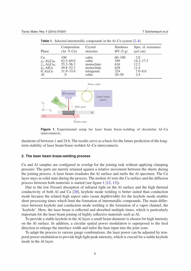
Cu and Al samples are configured in overlap for the joining task without applying clamping pressure. The parts are merely retained against a relative movement between the sheets during the joining process. A laser beam irradiates the Al surface and melts the Al specimen. The Cu layer stays in solid state during the process. The molten Al wets the Cu surface and the diffusion process between both materials is started (see figure 1 [12, 13]).
Due to the low Fresnel absorption of infrared light on the Al surface and the high thermal conductivity of both Al and Cu [20], keyhole mode welding is better suited than conduction mode because the related high aspect ratio (seam depth/width) for the keyhole mode enables short processing times which limit the formation of intermetallic compounds. The main differ-ence between keyhole and conduction mode welding is the formation of a vapor channel, the ‘keyhole’. Here, the laser beam is reflected and absorbed multiple times, which is particularly important for the laser beam joining of highly reflective materials such as Al.
To provide a stable keyhole in the Al layer a small beam diameter is chosen for high intensity on the Al surface. In addition, a circular spatial power modulation is superposed to the feed direction to enlarge the interface width and tailor the heat input into the joint zone.
To adapt the process to various gauge combinations, the laser power can be adjusted by tem-poral power modulation to provide high light peak intensity, which is crucial for a stable keyhole mode in the Al layer.
Table 1. Selected intermetallic compounds in the Al–Cu system [2–4].
PhaseComposition (At. % Cu)
Crystal structure
Hardness HV (5 g)
Spec. el. resistance (μΩ cm)
Cu 100 cubic 60–100 2.0γ2, Al4Cu9 62.5–69.0 cubic 549 14.2–17.3ζ2, Al3Cu4 55.2–56.3 monoclinic 616 12.2η2, AlCu 49.8–52.3 monoclinic 628 11.4θ, Al2Cu 31.9–33.0 tetragonal 324 7.0–8.0Al 0 cubic 20–50 2.4
Figure 1. Experimental setup for laser beam braze-welding of dissimilar Al–Cu interconnects.
T Solchenbach et al
4
Transl. Mater. Res. 1 (2014) 015001
For the experiments EN-AW1050A Al and SF-Cu Cu samples (both in half-hard state) were used, with gauges of 210 and 200 µm, respectively. These materials are commonly used for electric and electronic applications.
Before laser joining, the samples were cleaned with acetone. A surface pre-conditioning, e.g. by means of etching or using flux for better wetability, was not applied in order to keep both the pre-processing and the joining process as simple as possible. Argon shielding gas of quality 4.6 was applied by a four-tube nozzle perpendicular to the feed direction with a gas flow of 9 l min − 1.
For the braze-welding experiments, a single mode Trumpf TruFiber 400 fiber laser with a near-infrared wavelength of λ = 1070 nm and a maximum power of P = 400 W was used in com-bination with a Scanlab HS20 2D f-θ-scanner head (figure 1). A spot diameter of 31 µm can thus be obtained with the focus 1 mm below the Al surface.
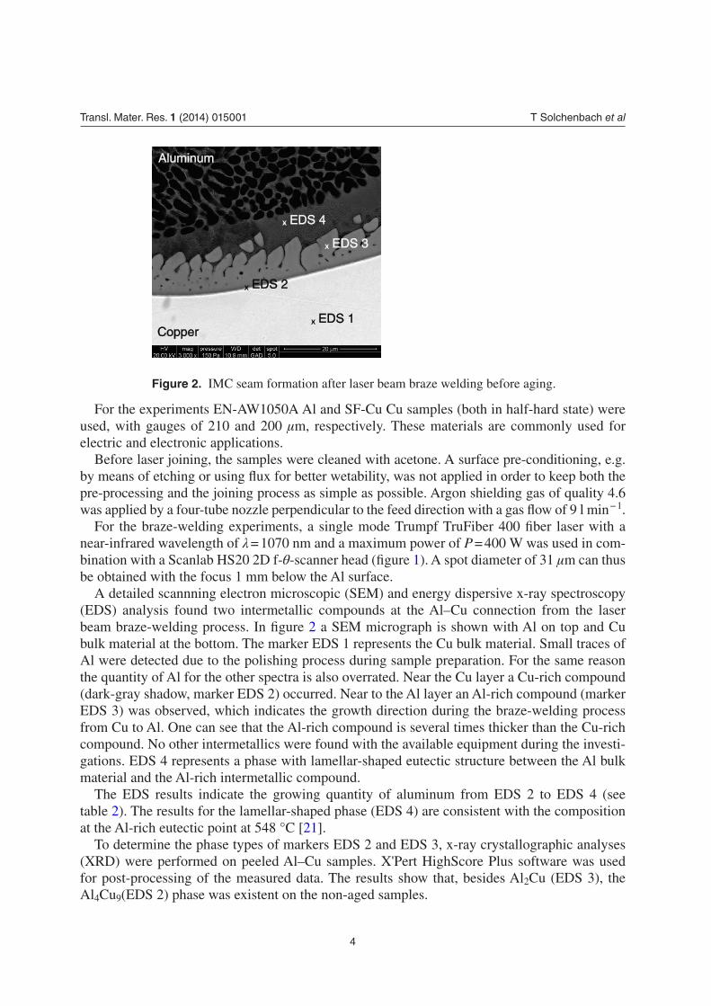
A detailed scannning electron microscopic (SEM) and energy dispersive x-ray spectroscopy (EDS) analysis found two intermetallic compounds at the Al–Cu connection from the laser beam braze-welding process. In figure 2 a SEM micrograph is shown with Al on top and Cu bulk material at the bottom. The marker EDS 1 represents the Cu bulk material. Small traces of Al were detected due to the polishing process during sample preparation. For the same reason the quantity of Al for the other spectra is also overrated. Near the Cu layer a Cu-rich compound (dark-gray shadow, marker EDS 2) occurred. Near to the Al layer an Al-rich compound (marker EDS 3) was observed, which indicates the growth direction during the braze-welding process from Cu to Al. One can see that the Al-rich compound is several times thicker than the Cu-rich compound. No other intermetallics were found with the available equipment during the investi-gations. EDS 4 represents a phase with lamellar-shaped eutectic structure between the Al bulk material and the Al-rich intermetallic compound.
The EDS results indicate the growing quantity of aluminum from EDS 2 to EDS 4 (see table 2). The results for the lamellar-shaped phase (EDS 4) are consistent with the composition at the Al-rich eutectic point at 548 °C [21].
To determine the phase types of markers EDS 2 and EDS 3, x-ray crystallographic analyses (XRD) were performed on peeled Al–Cu samples. X'Pert HighScore Plus software was used for post-processing of the measured data. The results show that, besides Al2Cu (EDS 3), the Al4Cu9(EDS 2) phase was existent on the non-aged samples.
Figure 2. IMC seam formation after laser beam braze welding before aging.
Aluminum
Copper
. EDS 4
. EDS 3
. EDS 2
. EDS 1
x
x
x
x
T Solchenbach et al
5
Transl. Mater. Res. 1 (2014) 015001
3. Apparatus and procedures for the aging tests
Thermal aging was realized by heating the Al–Cu interconnects in an electric furnace for dif-ferent durations and at different temperatures, while the furnace was capable of maintaining the temperature to within ± 2 °C. A temperature range of 200–500 °C was used in increments of 100 °C, since the growth rate of intermetallic compounds is dominated by volume diffusion in this range [22].
Electrical aging was performed by heating the samples with a dc of 200 amperes in air with different polarities. A joint length of 4 mm was chosen to obtain a current density of 1.05 E4 A cm − 2, which corresponds to the lower limit of electromigration effects (1E3–1E6 A cm − 2) [14, 23]. The interconnects were annealed by Joule heat, caused by the current.
A sample size of N = 3 for thermal aging and N = 2 for electrical aging was chosen.Subsequent to the aging experiments, the interface was examined by means of optical and
scanning electron microscopy to measure the layer thickness and determine the chemical com-position of the different compounds. Cross-section micrographs were taken from the center of the interface. X-ray diffraction (XRD) was used for the crystallographic assignment of the intermetallic compounds.
The following devices were used during the experiments:
•CarboliteELFfurnaceforthermalaging; •AgilentTechnologyN8733Adcpowersupplyfordccurrentcycling; •LeicaDM4000Mopticalmicroscope; •FEIQuantaFED200scanningelectronmicroscope; •GENESISXM4iEDSx-rayenergydispersivespectrometer; •HAMEGHMP4040powersupplyforresistancemeasurement; •KeithleyIntegraSeriesModel2700multimeter/dataacquisitionsystem; •PanalyticalX’PertProMPDXRDequipment.
4. Thermal aging results
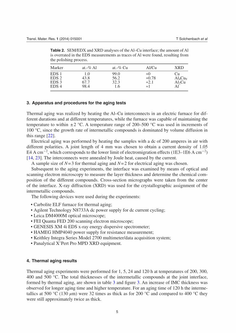
Thermal aging experiments were performed for 1, 5, 24 and 120 h at temperatures of 200, 300, 400 and 500 °C. The total thicknesses of the intermetallic compounds at the joint interface, formed by thermal aging, are shown in table 3 and figure 3. An increase of IMC thickness was observed for longer aging time and higher temperature. For an aging time of 120 h the interme-tallics at 500 °C (130 µm) were 32 times as thick as for 200 °C and compared to 400 °C they were still approximately twice as thick.
Table 2. SEM/EDXandXRDanalysesoftheAl–Cuinterface;theamountofAlis overrated in the EDS measurements as traces of Al were found, resulting from the polishing process.
Marker at.-% Al at.-% Cu Al/Cu XRD
EDS 1 1.0 99.0 ≈0 CuEDS 2 43.8 56.2 ≈0.78 Al4Cu9EDS 3 67.7 32.3 ≈2.1 Al2CuEDS 4 98.4 1.6 ≈1 Al
T Solchenbach et al
6
Transl. Mater. Res. 1 (2014) 015001
The main driving force for the intermetallic layer growth is the atomic diffusion between Al and Cu. In general, the phase growth is controlled by volume diffusion and the square root time law can be used [22]. Hence, the relation between IMC layer thickness x and the time t at a con-stant temperature can be described by equation (1):
= +x K t x· ,202 (1)
where x0 is the thickness of the intermetallic compounds resulting from the braze-welding pro-cess (x0 = 3.2 µm) and K is the growth rate constant for a given temperature and represents the gradient of each curve in figure 3. The rate constants were computed and are summarized in table 4. K is defined by equation (2):
= −K K e· ,·0Q
R T (2)
where K0 is the frequency factor, Q the activation energy, R the ideal gas constant and T the absolute temperature [22].
Table 3. Total thickness of intermetallic compounds x (µm) at the Al–Cu interface for different aging temperatures and times in a furnace.
Total thickness of IMC × (μm)
Time (hours) Temperature T (°C)
200 300 400 5001 2.5 4.8 4.1 18.05 3.0 5.8 6.2 35.024 3.0 8.8 23.4 69.8120 4.0 17.1 53.2 130.8
Figure 3. Phase growth of intermetallic compounds at the Al–Cu interface annealed in furnace.
0 100 200 300 400 500 600 7000
50
100
150
Time1/2 [s1/2]
Inte
rmet
allic
thic
knes
s [µ
m]
200 °C300 °C400 °C500 °C
T Solchenbach et al
7
Transl. Mater. Res. 1 (2014) 015001
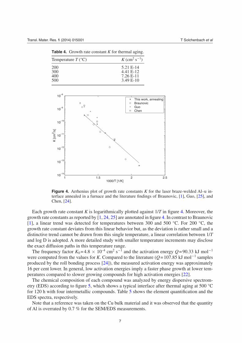
Each growth rate constant K is logarithmically plotted against 1/T in figure 4. Moreover, the growth rate constants as reported by [1, 24, 25] are annotated in figure 4. In contrast to Braunovic [1], a linear trend was detected for temperatures between 300 and 500 °C. For 200 °C, the growth rate constant deviates from this linear behavior but, as the deviation is rather small and a distinctive trend cannot be drawn from this single temperature, a linear correlation between 1/T and log D is adopted. A more detailed study with smaller temperature increments may disclose the exact diffusion paths in this temperature range.
The frequency factor K0 = 4.8 × 10⁻⁴ cm2 s − 1 and the activation energy Q = 90.33 kJ mol − 1 were computed from the values for K. Compared to the literature (Q = 107.85 kJ mol − 1 samples produced by the roll bonding process [24]), the measured activation energy was approximately 16 per cent lower. In general, low activation energies imply a faster phase growth at lower tem-peratures compared to slower growing compounds for high activation energies [22].
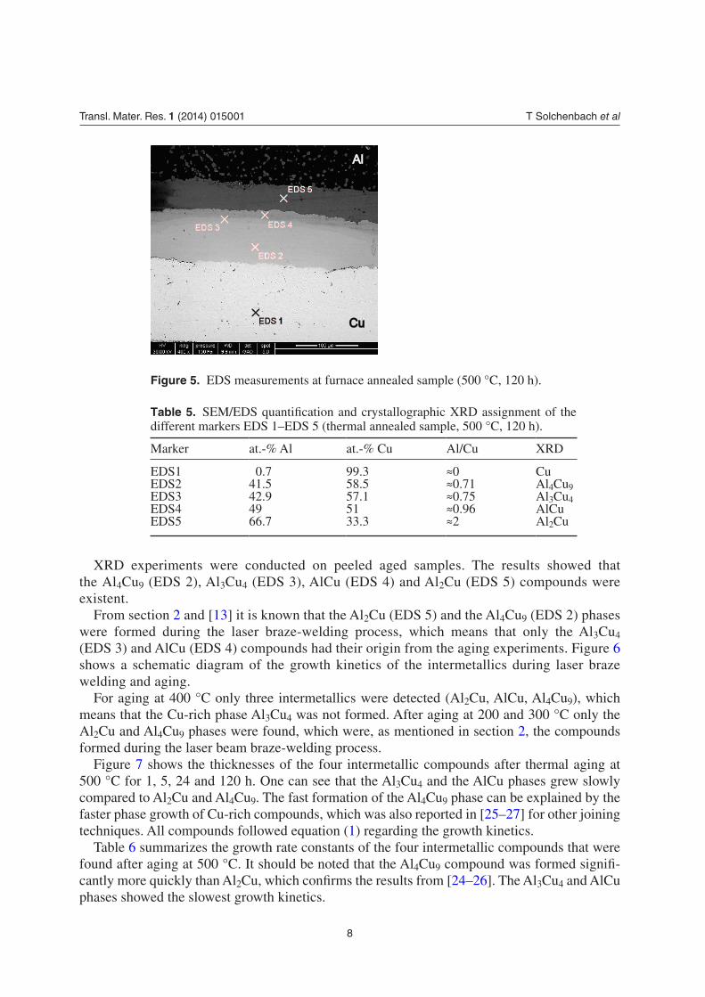
The chemical composition of each compound was analyzed by energy dispersive spectrom-etry (EDS) according to figure 5, which shows a typical interface after thermal aging at 500 °C for 120 h with four intermetallic compounds. Table 5 shows the element quantification and the EDS spectra, respectively.
Note that a reference was taken on the Cu bulk material and it was observed that the quantity of Al is overrated by 0.7 % for the SEM/EDS measurements.
Figure 4. Arrhenius plot of growth rate constants K for the laser braze-welded Al–u in-terface annealed in a furnace and the literature findings of Braunovic, [1],Guo,[25], and Chen, [24].
1 1.5 2 2.510
−14
10−13
10−12
10−11
10−10
10−9
10−8
1000/T [1/K]
K [c
m2 /s
]
This work, annealingBraunovicGuoChen
Table 4. GrowthrateconstantK for thermal aging.
Temperature T (°C) K (cm2 s − 1)
200 5.21 E-14300 4.41 E-12400 7.26 E-11500 3.49 E-10
T Solchenbach et al
8
Transl. Mater. Res. 1 (2014) 015001
XRD experiments were conducted on peeled aged samples. The results showed that the Al4Cu9 (EDS 2), Al3Cu4 (EDS 3), AlCu (EDS 4) and Al2Cu (EDS 5) compounds were existent.
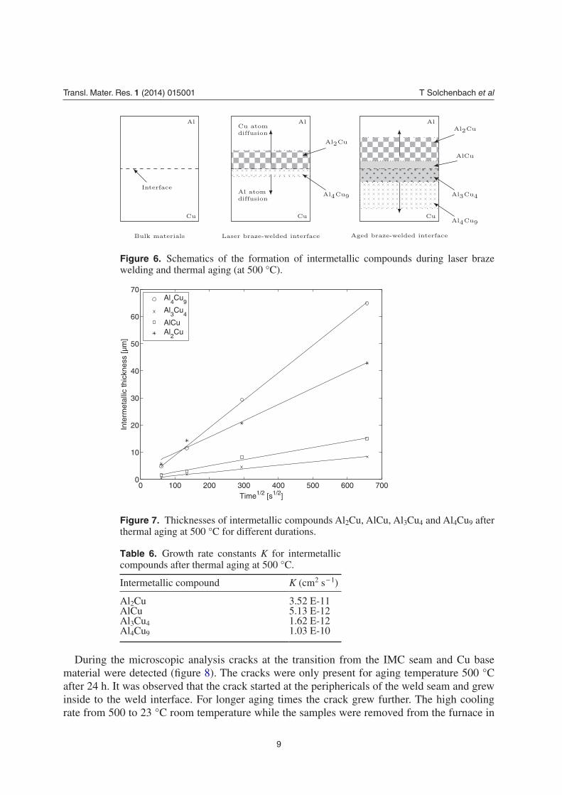
From section 2 and [13] it is known that the Al2Cu (EDS 5) and the Al4Cu9 (EDS 2) phases were formed during the laser braze-welding process, which means that only the Al3Cu4 (EDS 3) and AlCu (EDS 4) compounds had their origin from the aging experiments. Figure 6 shows a schematic diagram of the growth kinetics of the intermetallics during laser braze welding and aging.
For aging at 400 °C only three intermetallics were detected (Al2Cu, AlCu, Al4Cu9), which means that the Cu-rich phase Al3Cu4 was not formed. After aging at 200 and 300 °C only the Al2Cu and Al4Cu9 phases were found, which were, as mentioned in section 2, the compounds formed during the laser beam braze-welding process.
Figure 7 shows the thicknesses of the four intermetallic compounds after thermal aging at 500 °C for 1, 5, 24 and 120 h. One can see that the Al3Cu4 and the AlCu phases grew slowly compared to Al2Cu and Al4Cu9. The fast formation of the Al4Cu9 phase can be explained by the faster phase growth of Cu-rich compounds, which was also reported in [25–27] for other joining techniques. All compounds followed equation (1) regarding the growth kinetics.
Table 6 summarizes the growth rate constants of the four intermetallic compounds that were found after aging at 500 °C. It should be noted that the Al4Cu9 compound was formed signifi-cantly more quickly than Al2Cu, which confirms the results from [24–26]. The Al3Cu4 and AlCu phases showed the slowest growth kinetics.
Figure 5. EDS measurements at furnace annealed sample (500 °C, 120 h).
Cu
Al
Table 5. SEM/EDS quantification and crystallographic XRD assignment of the different markers EDS 1–EDS 5 (thermal annealed sample, 500 °C, 120 h).
Marker at.-% Al at.-% Cu Al/Cu XRD
EDS1 0.7 99.3 ≈0 CuEDS2 41.5 58.5 ≈0.71 Al4Cu9EDS3 42.9 57.1 ≈0.75 Al3Cu4EDS4 49 51 ≈0.96 AlCuEDS5 66.7 33.3 ≈2 Al2Cu
T Solchenbach et al
9
Transl. Mater. Res. 1 (2014) 015001
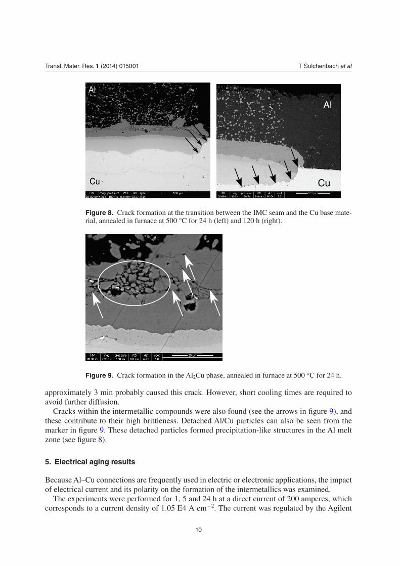
During the microscopic analysis cracks at the transition from the IMC seam and Cu base material were detected (figure 8). The cracks were only present for aging temperature 500 °C after 24 h. It was observed that the crack started at the periphericals of the weld seam and grew inside to the weld interface. For longer aging times the crack grew further. The high cooling rate from 500 to 23 °C room temperature while the samples were removed from the furnace in
Figure 7. Thicknesses of intermetallic compounds Al2Cu, AlCu, Al3Cu4 and Al4Cu9 after thermal aging at 500 °C for different durations.
0 100 200 300 400 500 600 7000
10
20
30
40
50
60
70
Time1/2 [s1/2]
Inte
rmet
allic
thic
knes
s [µ
m]
Al4Cu
9
Al3Cu
4
AlCuAl
2Cu
Table 6. Growth rate constantsK for intermetallic compounds after thermal aging at 500 °C.
Intermetallic compound K (cm2 s − 1)
Al2Cu 3.52 E-11AlCu 5.13 E-12Al3Cu4 1.62 E-12Al4Cu9 1.03 E-10
Figure 6. Schematics of the formation of intermetallic compounds during laser braze welding and thermal aging (at 500 °C).
T Solchenbach et al
10
Transl. Mater. Res. 1 (2014) 015001
approximately 3 min probably caused this crack. However, short cooling times are required to avoid further diffusion.
Cracks within the intermetallic compounds were also found (see the arrows in figure 9), and these contribute to their high brittleness. Detached Al/Cu particles can also be seen from the marker in figure 9. These detached particles formed precipitation-like structures in the Al melt zone (see figure 8).
5. Electrical aging results
Because Al–Cu connections are frequently used in electric or electronic applications, the impact of electrical current and its polarity on the formation of the intermetallics was examined.
The experiments were performed for 1, 5 and 24 h at a direct current of 200 amperes, which corresponds to a current density of 1.05 E4 A cm − 2. The current was regulated by the Agilent
Figure 9. Crack formation in the Al2Cu phase, annealed in furnace at 500 °C for 24 h.
Figure 8. Crack formation at the transition between the IMC seam and the Cu base mate-rial, annealed in furnace at 500 °C for 24 h (left) and 120 h (right).
Cu
Al
T Solchenbach et al
11
Transl. Mater. Res. 1 (2014) 015001
equipment. The applied voltage level was between 0.96 V at a thermal steady state at the begin-ning of the tests and 0.98 V after 24 h, which implies that the electrical restistance of the sam-ples increased during the tests, most likely due to the growth of intermetallic compounds at the interface. However, a detailed analysis of the contact resistance was not in the scope of the experiments and will be the goal of future investigations.
The interconnects were annealed by Joule heat. An average sample temperature of 345 ± 15 °C was measured with a type K thermocouple, which was attached with heat-conductive paste on the weld seam.
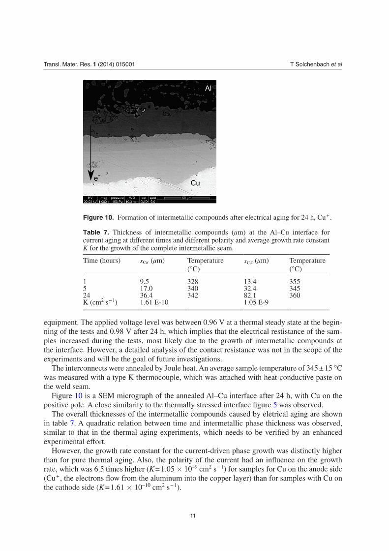
Figure 10 is a SEM micrograph of the annealed Al–Cu interface after 24 h, with Cu on the positive pole. A close similarity to the thermally stressed interface figure 5 was observed.
The overall thicknesses of the intermetallic compounds caused by eletrical aging are shown in table 7. A quadratic relation between time and intermetallic phase thickness was observed, similar to that in the thermal aging experiments, which needs to be verified by an enhanced experimental effort.
However, the growth rate constant for the current-driven phase growth was distinctly higher than for pure thermal aging. Also, the polarity of the current had an influence on the growth rate, which was 6.5 times higher (K = 1.05 × 10⁻⁹ cm2 s − 1) for samples for Cu on the anode side (Cu + , the electrons flow from the aluminum into the copper layer) than for samples with Cu on the cathode side (K = 1.61 × 10⁻¹⁰ cm2 s − 1).
Figure 10. Formation of intermetallic compounds after electrical aging for 24 h, Cu + .
Cu
Al
e-
Table 7. Thickness of intermetallic compounds (µm) at the Al–Cu interface for current aging at different times and different polarity and average growth rate constant K for the growth of the complete intermetallic seam.
Time (hours) xCu- (µm) Temperature (°C)
+xCu (µm) Temperature (°C)
1 9.5 328 13.4 3555 17.0 340 32.4 34524 36.4 342 82.1 360K (cm2 s − 1) 1.61 E-10 1.05 E-9
T Solchenbach et al
12
Transl. Mater. Res. 1 (2014) 015001
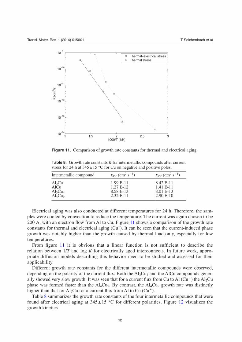
Electrical aging was also conducted at different temperatures for 24 h. Therefore, the sam-ples were cooled by convection to reduce the temperature. The current was again chosen to be 200 A, with an electron flow from Al to Cu. Figure 11 shows a comparison of the growth rate constants for thermal and electrical aging (Cu+). It can be seen that the current-induced phase growth was notably higher than the growth caused by thermal load only, especially for low temperatures.
From figure 11 it is obvious that a linear function is not sufficient to describe the relation between 1/T and log K for electrically aged interconnects. In future work, appro-priate diffusion models describing this behavior need to be studied and assessed for their applicability.
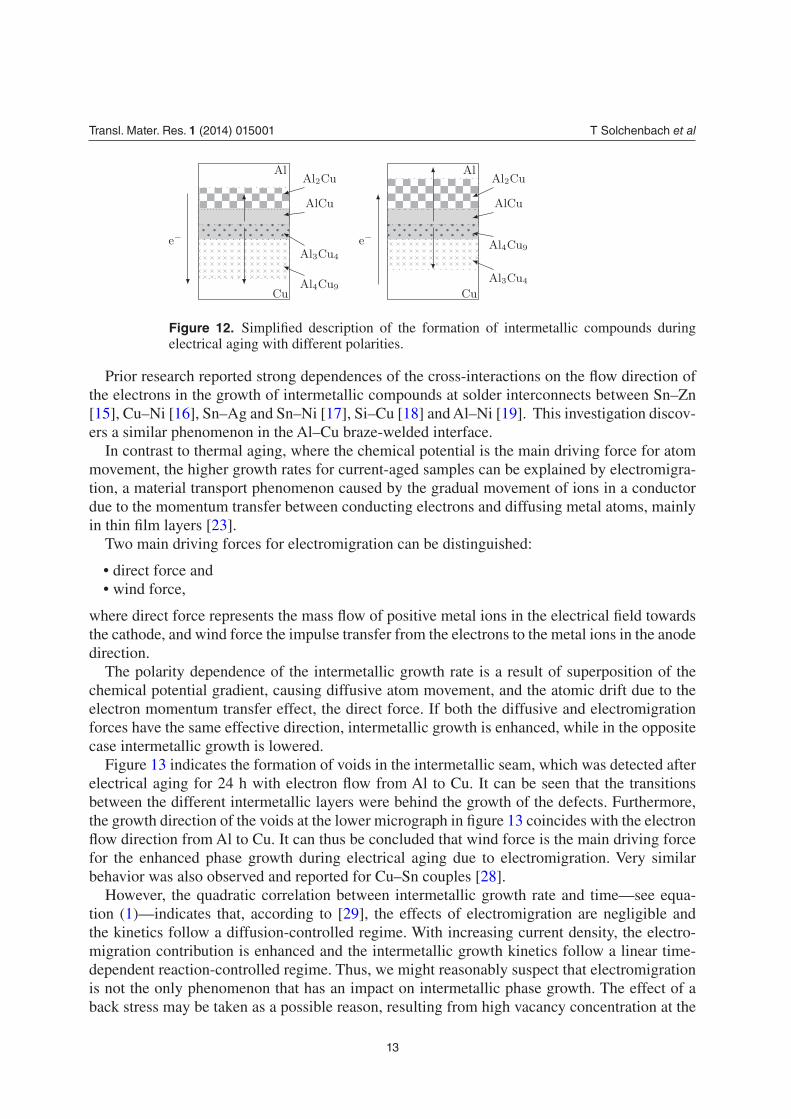
Different growth rate constants for the different intermetallic compounds were observed, depending on the polarity of the current flux. Both the Al3Cu4 and the AlCu compounds gener-ally showed very slow growth. It was seen that for a current flux from Cu to Al (Cu − ) the Al2Cu phase was formed faster than the Al4Cu9. By contrast, the Al4Cu9 growth rate was distinctly higher than that for Al2Cu for a current flux from Al to Cu (Cu + ).
Table 8 summarizes the growth rate constants of the four intermetallic compounds that were found after electrical aging at 345 ± 15 °C for different polarities. Figure 12 visualizes the growth kinetics.
Figure 11. Comparison of growth rate constants for thermal and electrical aging.
1 1.5 2 2.5 310
−14
10−13
10−12
10−11
10−10
10−9
1000/T [1/K]
K [c
m2 /s
]Thermal−electrical stressThermal stress
Table 8. GrowthrateconstantsK for intermetallic compounds after current stress for 24 h at 345 ± 15 °C for Cu on negative and positive poles.
Intermetallic compound KCu- (cm2 s − 1) +KCu (cm2 s − 1)
Al2Cu 1.99 E-11 8.42 E-11AlCu 1.27 E-12 1.41 E-11Al3Cu4 8.58 E-13 8.01 E-13Al4Cu9 2.32 E-11 2.90 E-10
T Solchenbach et al
13
Transl. Mater. Res. 1 (2014) 015001
Prior research reported strong dependences of the cross-interactions on the flow direction of the electrons in the growth of intermetallic compounds at solder interconnects between Sn–Zn [15], Cu–Ni [16], Sn–Ag and Sn–Ni [17], Si–Cu [18] and Al–Ni [19]. This investigation discov-ers a similar phenomenon in the Al–Cu braze-welded interface.
In contrast to thermal aging, where the chemical potential is the main driving force for atom movement, the higher growth rates for current-aged samples can be explained by electromigra-tion, a material transport phenomenon caused by the gradual movement of ions in a conductor due to the momentum transfer between conducting electrons and diffusing metal atoms, mainly in thin film layers [23].
Two main driving forces for electromigration can be distinguished:
•directforceand •windforce,
where direct force represents the mass flow of positive metal ions in the electrical field towards the cathode, and wind force the impulse transfer from the electrons to the metal ions in the anode direction.
The polarity dependence of the intermetallic growth rate is a result of superposition of the chemical potential gradient, causing diffusive atom movement, and the atomic drift due to the electron momentum transfer effect, the direct force. If both the diffusive and electromigration forces have the same effective direction, intermetallic growth is enhanced, while in the opposite case intermetallic growth is lowered.
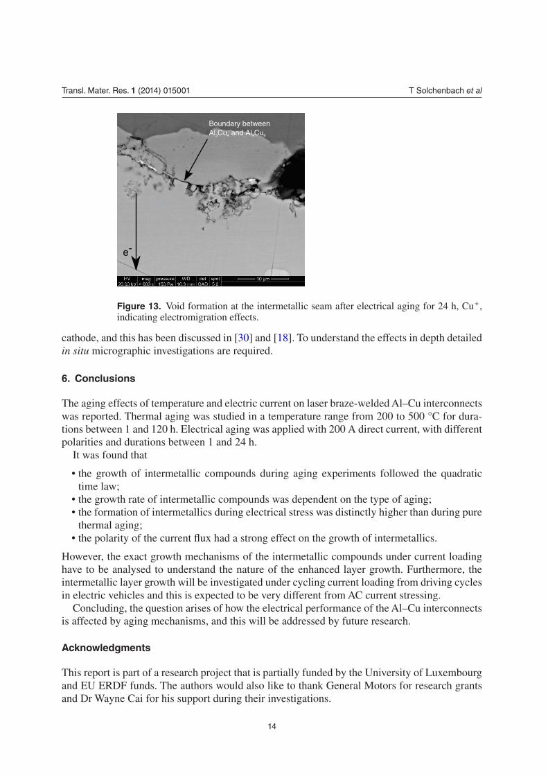
Figure 13 indicates the formation of voids in the intermetallic seam, which was detected after electrical aging for 24 h with electron flow from Al to Cu. It can be seen that the transitions between the different intermetallic layers were behind the growth of the defects. Furthermore, the growth direction of the voids at the lower micrograph in figure 13 coincides with the electron flow direction from Al to Cu. It can thus be concluded that wind force is the main driving force for the enhanced phase growth during electrical aging due to electromigration. Very similar behavior was also observed and reported for Cu–Sn couples [28].
However, the quadratic correlation between intermetallic growth rate and time—see equa-tion (1)—indicates that, according to [29], the effects of electromigration are negligible and the kinetics follow a diffusion-controlled regime. With increasing current density, the electro-migration contribution is enhanced and the intermetallic growth kinetics follow a linear time-dependent reaction-controlled regime. Thus, we might reasonably suspect that electromigration is not the only phenomenon that has an impact on intermetallic phase growth. The effect of a back stress may be taken as a possible reason, resulting from high vacancy concentration at the
Figure 12. Simplified description of the formation of intermetallic compounds during electrical aging with different polarities.
T Solchenbach et al
14
Transl. Mater. Res. 1 (2014) 015001
cathode, and this has been discussed in [30] and [18]. To understand the effects in depth detailed in situ micrographic investigations are required.
6. Conclusions
The aging effects of temperature and electric current on laser braze-welded Al–Cu interconnects was reported. Thermal aging was studied in a temperature range from 200 to 500 °C for dura-tions between 1 and 120 h. Electrical aging was applied with 200 A direct current, with different polarities and durations between 1 and 24 h.
It was found that
•the growth of intermetallic compounds during aging experiments followed the quadratictimelaw;
•thegrowthrateofintermetalliccompoundswasdependentonthetypeofaging; •theformationofintermetallicsduringelectricalstresswasdistinctlyhigherthanduringpure
thermalaging; •thepolarityofthecurrentfluxhadastrongeffectonthegrowthofintermetallics.
However, the exact growth mechanisms of the intermetallic compounds under current loading have to be analysed to understand the nature of the enhanced layer growth. Furthermore, the intermetallic layer growth will be investigated under cycling current loading from driving cycles in electric vehicles and this is expected to be very different from AC current stressing.
Concluding, the question arises of how the electrical performance of the Al–Cu interconnects is affected by aging mechanisms, and this will be addressed by future research.
Acknowledgments
This report is part of a research project that is partially funded by the University of Luxembourg andEUERDFfunds.TheauthorswouldalsoliketothankGeneralMotorsforresearchgrantsand Dr Wayne Cai for his support during their investigations.
Figure 13. Void formation at the intermetallic seam after electrical aging for 24 h, Cu + , indicating electromigration effects.
e-
Boundary between Al3Cu4 and Al4Cu9
T Solchenbach et al
15
Transl. Mater. Res. 1 (2014) 015001
References
[1] Braunovic M 2007 J. Zhejiang Univ. 8 343–56 [2] Westbrook J H and Fleischer 2000 R L Structural Applications of Intermetallic Compounds (New York: Wiley) [3] Pfeifer S,Grossmann S,Freudenberger R,Willing HandKappl H2012Characterizationofintermetalliccompoundsin
Al–Cu-bimetallic interfaces IEEE 58th Holm Conf. on Electrical Contacts (Portland, 2012) pp 1–6 [4] Wulff F W, Breach C D, Stephan D, Saraswati and Dittmer K J 2004 Characterisation of intermetallic growth in copper
and gold ball bonds on aluminium metallization Proc. 6th Electron. Packaging Technol. Conf. (Singapore, 2004) pp 348–53
[5] Lee S S, Kim T H, Hu S J, Cai W, Abell J A and Li J 2013 ASME J. Manuf. Sci. Eng. 135 021004 [6] Kang B, Cai W and Tan C A 2013 J. Manuf. Process. 6 218–32 [7] Bisadi H, Tavakoli A, Tour Sangsaraki M and Tour Sangsaraki K 2013 Mater. Des. 43 80–8 [8] Abbasi M, Karimi Taheri A and Salehi M T 2001 J. Alloys Compounds 319 233–41 [9] Schmidt P A, Schweier M and Zaeh M F 2012 Joining of lithium-ion batteries using laser beam welding: electrical losses
of welded aluminium and copper joints ICALEO 2012 (Anaheim, 2012) [10] Klages K2006Laserstrahl-MikroschweißenungleicherMetalledurchNahtschweissenmitgepulstenNd:YAG-Lasern
PhD Thesis RWTH Aachen[11] Hailat MM,Mian A,Chaudhury ZA,Newaz G,Patwa RandHerfurth HJ2012Microsyst. Technol. 18 103–12[12] Solchenbach T and Plapper P 2013 Proc. COMA 13 (Stellenbosch, 2013) pp 131–6 [13] Solchenbach T and Plapper P 2013 Opt. Laser Technol. 54 249–56[14] Braunovic M and Alexandrov N 1994 IEEE Trans. Components Packag. Manuf. Technol. A 17 78–85[15] Zhang XF,Guo JDandShang JK2007Scr. Mater. 57 513–6[16] Wu W H, Chung H L, Chen C N and Ho C E 2009 J. Electron. Mater. 38 2563–72[17] Chen C-M and Chen S-W 2002 Acta Mater. 50 2461–9[18] Gan HandTu KN2005J. Appl. Phys. 97 063514 [19] Liu W C, Chen S W and Chen C M 1998 J. Electron. Mater. 27 L6–9[20] Poprawe R 2005 Lasertechnik für die fertigung grundlagen, perspektiven und beispiele für den innovativen ingenieur mit
26 Tabellen [21] ASM 1992 ASM Handbook Volume 03: Alloy Phase Diagrams (Materials Park: ASM International) [22] Bäuerle D 2011 Laser Processing and Chemistry (Berlin: Springer)[23] Vinaricky E H 2002 Elektrische Kontakte, Werkstoffe und Anwendungen: Grundlagen, Technologien, Prüfverfahren 2
(Berlin: Springer) [24] Chen C and Hwang W 2007 Mater. trans. 48 1938–47[25] Guo Y,Liu G,Jin H,Shi ZandQiao G2011J. Mater. Sci. 46 2467–73[26] Lee K and Kwon Y 2013 Trans. Nonferrous Met. Soc. China 23 341–6[27] Kim H, Lee J, Paik K, Koh K, Won J, Choe S, Lee J, Moon J and Park Y 2003 IEEE Trans. Components Packag.
Technol. 26 367–74[28] Chen L, Huang M and Zhou S 2010 J. Alloys Compounds 504 535–41[29] Chao H L, Chae S H, Zhang X, Lu K H, Im J and Ho P S 2006 Kinetic analysis of current enhanced intermetallic growth
and its effect on electromigration reliability of solder joints IEEE Int. Reliab. Phys. Symp. Proc., 44th Annual (San Jose, 2006) pp 250–5
[30] Blech I A and Herring C 1976 Appl. Phys. Lett. 29 131
Related Documents