1 © 2015 ANSYS, Inc. November 11, 2015 Thermal and Color-aware Reliability Verification for Sub-16nm FinFET Designs Norman Chang VP & Sr. Product Strategist, Apache BU GSA, Nov. 2015

Welcome message from author
This document is posted to help you gain knowledge. Please leave a comment to let me know what you think about it! Share it to your friends and learn new things together.
Transcript

1 © 2015 ANSYS, Inc. November 11, 2015
Thermal and Color-aware Reliability Verification for Sub-16nm FinFET Designs
Norman Chang VP & Sr. Product Strategist, Apache BU
GSA, Nov. 2015

2 © 2015 ANSYS, Inc. November 11, 2015
Sub-16nm FinFET Migration Challenges
65nm
• Static IR • Dynamic IR
40nm
• Low Power • Leakage Opt. • Chip + Package • Static IR • Dynamic IR
28nm
• Reliability • Power/Signal EM • Low Power • Leakage Opt. • Chip + Package • Static IR • Dynamic IR
20nm
• Advanced Reliability
• ESD • Power/Signal EM • Low Power • Leakage Opt. • Chip + Package • Static IR • Dynamic IR
16nm
• Dev/Wire Selfheat • Chip-Pkg Co-design • Advanced Reliability • ESD • Power/Signal EM • Low Power • Leakage Opt. • Chip + Package • Static IR • Dynamic IR
• Increasing number of checks for advanced technology nodes
• Sign-off mandates advanced checks for the FinFET nodes
10nm
• Color-aware R/C • Color-aware EM • Dev/Wire Selfheat • Advanced Reliability • ESD • Power/Signal EM • Low Power • Leakage Opt. • Chip + Package • Static IR • Dynamic IR
3 © 2015 ANSYS, Inc. November 11, 2015
3D-ASIP, 2013
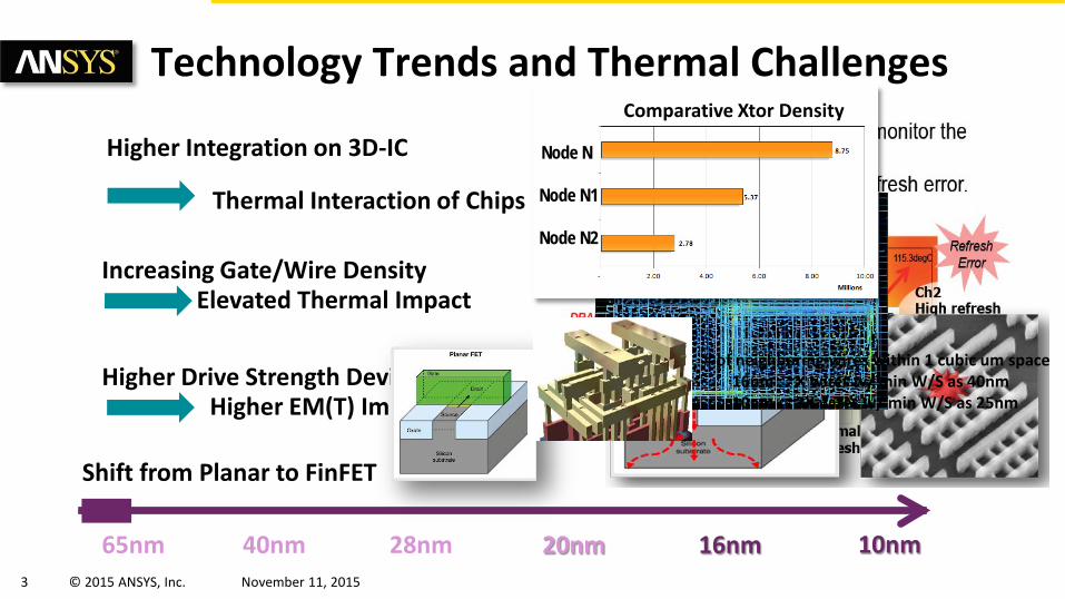
Technology Trends and Thermal Challenges
65nm 40nm 28nm 20nm 16nm
Higher Integration on 3D-IC
Thermal Interaction of Chips
Increasing Gate/Wire Density Elevated Thermal Impact
Higher Drive Strength Devices Higher EM(T) Impact
Shift from Planar to FinFET
10nm
# of neighboring wires within 1 cubic um space 16nm : ~X wires w/ min W/S as 40nm 10nm : ~3X wires w/ min W/S as 25nm
Node N
Node N1
Node N2
Comparative Xtor Density

4 © 2015 ANSYS, Inc. November 11, 2015
Overheating of Smartphones
• Overheating (> 45 ºC Skin Temp) due to increasing integration of functions on SoCs
• Higher concentration of power causing larger Delta-T and thermal gradient on wires
Fixed thru Throttling
http://tweakers.net/nieuws/102040/htc-verhelpt-hitteprobleem-one-m9-met.html
5 © 2015 ANSYS, Inc. November 11, 2015
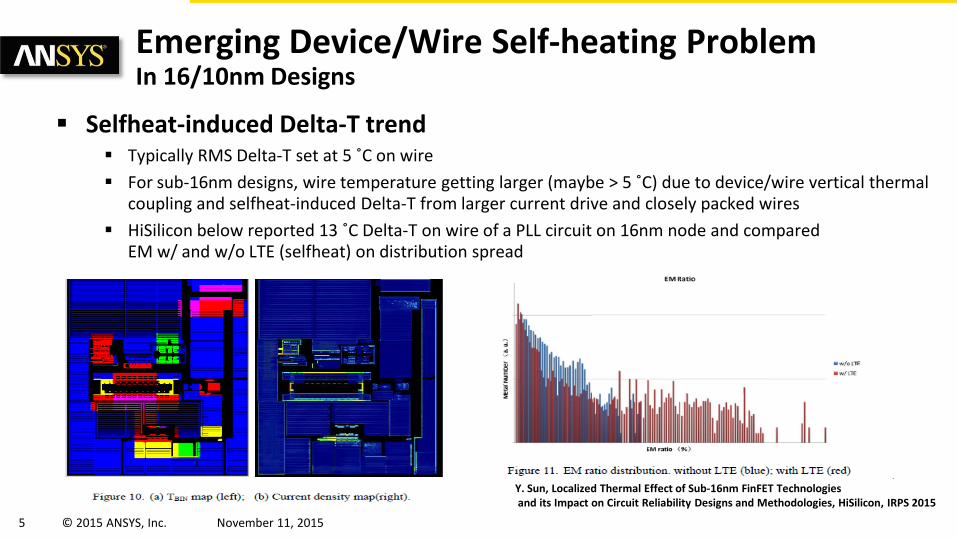
Emerging Device/Wire Self-heating Problem In 16/10nm Designs
Selfheat-induced Delta-T trend Typically RMS Delta-T set at 5 ˚C on wire For sub-16nm designs, wire temperature getting larger (maybe > 5 ˚C) due to device/wire vertical thermal
coupling and selfheat-induced Delta-T from larger current drive and closely packed wires HiSilicon below reported 13 ˚C Delta-T on wire of a PLL circuit on 16nm node and compared
EM w/ and w/o LTE (selfheat) on distribution spread
Y. Sun, Localized Thermal Effect of Sub-16nm FinFET Technologies and its Impact on Circuit Reliability Designs and Methodologies, HiSilicon, IRPS 2015
6 © 2015 ANSYS, Inc. November 11, 2015
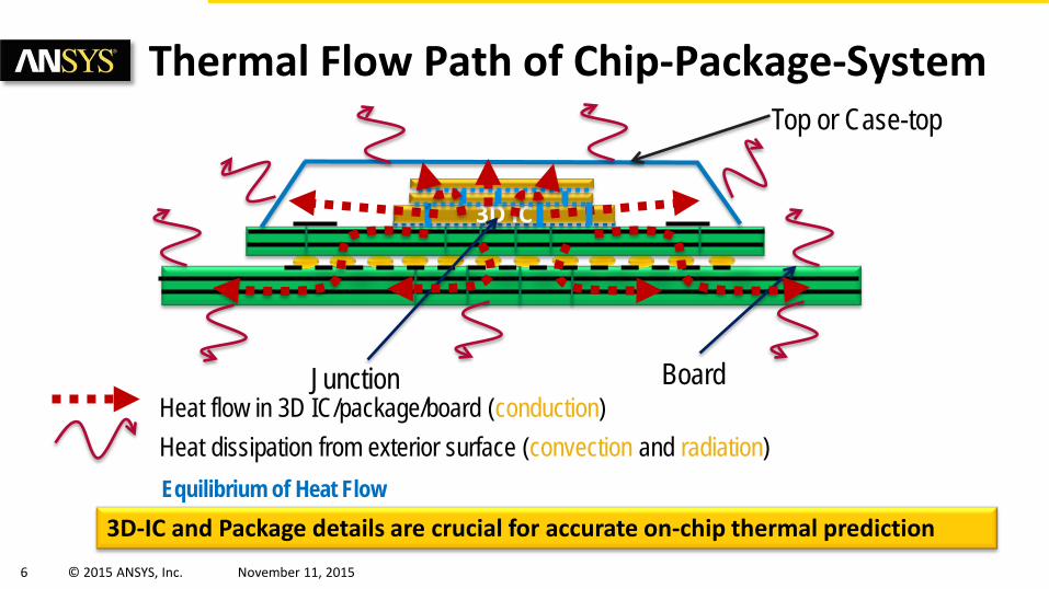
Thermal Flow Path of Chip-Package-System
3D IC
Equilibrium of Heat Flow 3D-IC and Package details are crucial for accurate on-chip thermal prediction
Top or Case-top
Board Junction Heat flow in 3D IC/package/board (conduction) Heat dissipation from exterior surface (convection and radiation)

7 © 2015 ANSYS, Inc. November 11, 2015
Achieving Thermal Integrity CPS Power-thermal Convergence
CTM Power
Dev/Wire Temp
BC
8 © 2015 ANSYS, Inc. November 11, 2015
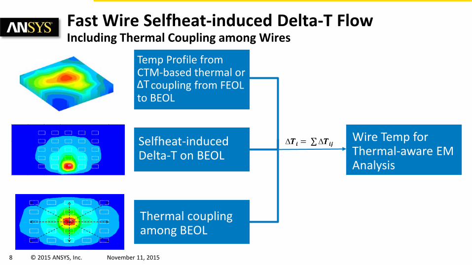
Fast Wire Selfheat-induced Delta-T Flow Including Thermal Coupling among Wires
Selfheat-induced Delta-T on BEOL
Thermal coupling among BEOL
Temp Profile from CTM-based thermal or coupling from FEOL to BEOL
Wire Temp for Thermal-aware EM Analysis
∆T
9 © 2015 ANSYS, Inc. November 11, 2015
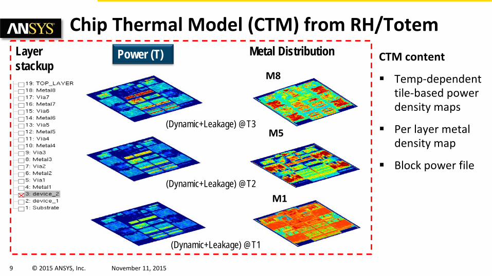
Chip Thermal Model (CTM) from RH/Totem Power (T) Layer
stackup M8
M5
M1
CTM content
Temp-dependent tile-based power density maps
Per layer metal density map
Block power file
(Dynamic+Leakage) @T1
(Dynamic+Leakage) @T2
(Dynamic+Leakage) @T3
Metal Distribution

10 © 2015 ANSYS, Inc. November 11, 2015
Power and Temperature Convergence Loops
CTM for each chip in 3D-IC : Lookup power map from temperature map
Updated Power in SoC or 3D-IC
Updated Temperature in 3D-IC 3D-IC Model
Automatic on-chip power-temperature iterations for converged solution

11 © 2015 ANSYS, Inc. November 11, 2015
Instance/Device Layer and BEOL Thermal Analysis
BEOL wire Delta-T calculation with fast selfheat-induced and thermal coupling among wires
Inst/Device Layer Thermal Analysis CMOS, BJT, PMIC, photonics, RFIC with CTM-based thermal analysis FinFET with measurement-based Delta-T calculation
12 © 2015 ANSYS, Inc. November 11, 2015
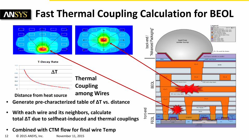
Fast Thermal Coupling Calculation for BEOL
Thermal Coupling among Wires
∆T
Distance from heat source • Generate pre-characterized table of ∆T vs. distance
• With each wire and its neighbors, calculate total ∆T due to selfheat-induced and thermal couplings
• Combined with CTM flow for final wire Temp

13 © 2015 ANSYS, Inc. November 11, 2015
Correlation of BEOL Fast Thermal Coupling to FEM
125
125.5
126
126.5
127
127.5
128
0 0.001 0.002 0.003 0.004 0.005
Tem
pera
ture
, C
Distance, mm
1Hot
2half
Lin-Sup
1hot_2half
center
1. 1Hot: 1x pwr on center wire only (FEM) 2. 2half: 0.5x pwr on side wires only (FEM) 3. Lin-Sup: (T1-125)+(T2-125)+125 4. 1hot_2half: 1x+0.5x+0.5x pwr (FEM)
Given 1&2, exact matches for #3 and #4 in Temperature distribution Accuracy of Linear-superposition verified
S. Pan, N. Chang, Fast Thermal Coupling, Ansys Inc., ECTC 2015

14 © 2015 ANSYS, Inc. November 11, 2015
Tote
m
Custom Design Self-heat Flow in Totem
Tech file / LIB / Dev Models GDS DSPF
w/ Signal RC Foundry SH Input
CTM P/G wire Irms info Signal wire Irms info
Perform Self-heat Analysis
Wire Self-heat Report Dev/OD Self-heat Report Dev/Wire Thermal Profile and Revised EM Report
Power EM Run Signal EM Run

15 © 2015 ANSYS, Inc. November 11, 2015
On-chip Thermal-Aware EM Flow Sentinel-TI RedHawk / Totem
Back-annotation
Power Library
Temperature
Device Thermal Profile Wire Temp for P/G and Sig
EM Violations Uniform Temperature
IC Design Package Design
CTM w/ foundry optional Input PG wire Irms
Signal wire Irms
3D-IC/SoC/Analog Thermal Analysis
w/ or w/o Thermal Coupling
CTM Model
Where is vertical thermal coupling from device to wire with RMS set at 5 ˚C for example EM Hotspot detection: Irms > Irms limit or > 5 ˚C

16 © 2015 ANSYS, Inc. November 11, 2015
Final Wire Temperature for Thermal-aware EM
Wire Temp Map
• With updated wire temperature map, users can click on the wire for wire temperature and other info J. Refaeli, Thermal-aware Reliability Check, Freescale Inc., DAC 2015
17 © 2015 ANSYS, Inc. November 11, 2015
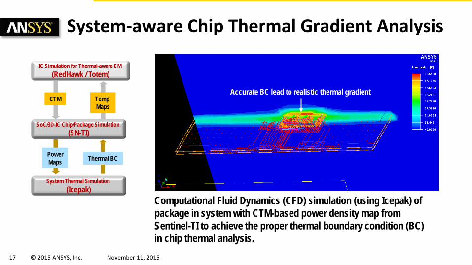
System-aware Chip Thermal Gradient Analysis
Computational Fluid Dynamics (CFD) simulation (using Icepak) of package in system with CTM-based power density map from Sentinel-TI to achieve the proper thermal boundary condition (BC) in chip thermal analysis.
Accurate BC lead to realistic thermal gradient
IC Simulation for Thermal-aware EM (RedHawk / Totem)
SoC/3D-IC Chip/Package Simulation (SN-TI)
System Thermal Simulation (Icepak)
CTM
Thermal BC Power Maps
Temp Maps

18 © 2015 ANSYS, Inc. November 11, 2015
Reliability Integrity Coverage
• Thermal-aware EM flow needed for tight EM margin on advanced technologies
• Thermal related reliability check is a must
On-chip thermal-aware EM
• Measurement-based FEOL/BEOL Delta-T formula for device/wire self-heat
• Table lookup-based thermal coupling between wires
On-chip FinFET Delta-T
• CTM-based thermal analysis on chip-package-system
• Per wire temperature available
SoC / 3D-IC Tmax
Thermal-aware EM
EM w/o Thermal

19 © 2015 ANSYS, Inc. November 11, 2015
BEOL metal, M1 to Mx, are DPT compliance
Resistance and EM calculation on BEOL are color-aware with “MASK” definition
Double Patterning Coloring Compliance
MASK A
MASK B

20 © 2015 ANSYS, Inc. November 11, 2015
Foundries (TSMC, Samsung, Intel, GlobalFoundries, etc.) Tools Qualified for FinFET Processes – RedHawk, Totem, PathFinder
• Color-aware Resistance correlation • Color-aware EM Rule handling • IR/EM Extraction and Analysis
Unique Metal Architecture •Special metal layers and color-based
R/C extraction •Complex via structures and shapes •Diffusion as interconnect structures
Enhanced Modeling •Dummy devices •Vertical resistance •Double patterning
Complex EM, ESD, Self-heat •Current-direction, metal topology based •Color-based EM rule and special handling •Width, temperature, self-heat, etc. •Pseudo-via, RMS, etc.
21 © 2015 ANSYS, Inc. November 11, 2015
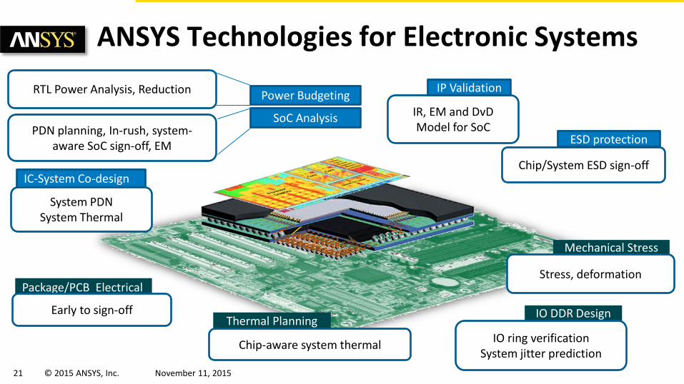
Package/PCB Electrical
Early to sign-off IO DDR Design
IO ring verification System jitter prediction
Thermal Planning
Chip-aware system thermal
Mechanical Stress
Stress, deformation
Power Budgeting
SoC Analysis
RTL Power Analysis, Reduction
PDN planning, In-rush, system-aware SoC sign-off, EM
IR, EM and DvD Model for SoC
IP Validation
Chip/System ESD sign-off
ESD protection
IC-System Co-design
System PDN System Thermal
ANSYS Technologies for Electronic Systems
Related Documents


