Citation: de Oliveira, I.R.; Tofoli, F.L.; Mendes, V.F. Thermal Analysis of Power Converters for DFIG-Based Wind Energy Conversion Systems during Voltage Sags. Energies 2022, 15, 3152. https://doi.org/10.3390/ en15093152 Academic Editor: Charalampos Baniotopoulos Received: 2 April 2022 Accepted: 25 April 2022 Published: 26 April 2022 Publisher’s Note: MDPI stays neutral with regard to jurisdictional claims in published maps and institutional affil- iations. Copyright: © 2022 by the authors. Licensee MDPI, Basel, Switzerland. This article is an open access article distributed under the terms and conditions of the Creative Commons Attribution (CC BY) license (https:// creativecommons.org/licenses/by/ 4.0/). energies Article Thermal Analysis of Power Converters for DFIG-Based Wind Energy Conversion Systems during Voltage Sags Igor Rodrigues de Oliveira 1 , Fernando Lessa Tofoli 2, * and Victor Flores Mendes 1 1 Graduate Program in Electrical Engineering, Federal University of Minas Gerais, Belo Horizonte 31270-901, Brazil; [email protected] (I.R.d.O.); [email protected] (V.F.M.) 2 Department of Electrical Engineering, Federal University of São João del-Rei, São João del-Rei 36307-352, Brazil * Correspondence: [email protected] Abstract: The doubly fed induction generator (DFIG) and back-to-back converter are very sensitive to power quality disturbances in grid-connected wind energy conversion systems (WECSs). Special attention has been given to protect the system from voltage sags, considering the introduction of several low-voltage ride-through (LVRT) techniques in the literature. However, only few works have really analyzed the behavior of power semiconductors during such phenomena in terms of the thermal stresses, whereas the existing studies are focused on balanced voltage sags only. In this context, this work presents a thermal profile analysis of power semiconductors in the grid- side converter (GSC) and rotor-side converter (RSC) considering a DFIG-based WECS submitted to symmetrical and asymmetrical voltage sags. The system is modeled using PLECS software and results on a 2.0 MW system are presented and thoroughly discussed. The results show that it is possible to meet the ride-through requirements during both balanced and unbalanced sags in terms of acceptable thermal stresses on the semiconductors as long as the back-to-back converter and its respective control system are properly designed. Keywords: DFIG; power semiconductors; thermal analysis; voltage sags; wind energy conversion systems 1. Introduction Wind energy has become an interesting alternative toward the solution of the world- wide energy crisis. In 2020, the global installed capacity of wind power plants reached 93 GW, this being the best result ever [1]. Considering that wind energy conversion systems (WECSs) are widely used in grid-connected applications, they should not only be tolerant to the occurrence of faults, but also have the ability to support the grid during voltage transients. In this sense, it is worth mentioning that the back-to-back converter is often the most sensitive element subjected to such undesirable phenomena [2]. It is well known that the doubly fed induction generator (DFIG) is one of the most popular choices for WECSs because it allows the operation with variable speed [3]. It also has the advantages of providing active and reactive power control, whereas the rated power of the power electronic converter is only a fraction of the generator rated power, that is, generally between 20% and 30%. However, DFIGs are very sensitive to grid disturbances, especially to voltage sags. The abrupt drop in grid voltage causes overvoltages and consequently overcurrents in the rotor windings, which could even destroy the converter if no protection systems are included [4,5]. WECSs must also comply with grid code requirements, among which low voltage ride through (LVRT) is of particular interest. Since 2003, the Brazilian Electric System Operator (ONS) stated that WECSs must incorporate the ability to maintain the operation without interrupting the power supply during abnormal conditions of the grid voltage [6]. In a recent revision in 2019, the grid code also incorporated the necessity of injecting reactive power to support the grid during faults or voltage dips. Energies 2022, 15, 3152. https://doi.org/10.3390/en15093152 https://www.mdpi.com/journal/energies

Welcome message from author
This document is posted to help you gain knowledge. Please leave a comment to let me know what you think about it! Share it to your friends and learn new things together.
Transcript
Citation: de Oliveira, I.R.; Tofoli, F.L.;
Mendes, V.F. Thermal Analysis of
Power Converters for DFIG-Based
Wind Energy Conversion Systems
during Voltage Sags. Energies 2022,
15, 3152. https://doi.org/10.3390/
en15093152
Academic Editor:
Charalampos Baniotopoulos
Received: 2 April 2022
Accepted: 25 April 2022
Published: 26 April 2022
Publisher’s Note: MDPI stays neutral
with regard to jurisdictional claims in
published maps and institutional affil-
iations.
Copyright: © 2022 by the authors.
Licensee MDPI, Basel, Switzerland.
This article is an open access article
distributed under the terms and
conditions of the Creative Commons
Attribution (CC BY) license (https://
creativecommons.org/licenses/by/
4.0/).
energies
Article
Thermal Analysis of Power Converters for DFIG-Based WindEnergy Conversion Systems during Voltage SagsIgor Rodrigues de Oliveira 1, Fernando Lessa Tofoli 2,* and Victor Flores Mendes 1
1 Graduate Program in Electrical Engineering, Federal University of Minas Gerais,Belo Horizonte 31270-901, Brazil; [email protected] (I.R.d.O.); [email protected] (V.F.M.)
2 Department of Electrical Engineering, Federal University of São João del-Rei,São João del-Rei 36307-352, Brazil
* Correspondence: [email protected]
Abstract: The doubly fed induction generator (DFIG) and back-to-back converter are very sensitiveto power quality disturbances in grid-connected wind energy conversion systems (WECSs). Specialattention has been given to protect the system from voltage sags, considering the introduction ofseveral low-voltage ride-through (LVRT) techniques in the literature. However, only few workshave really analyzed the behavior of power semiconductors during such phenomena in terms ofthe thermal stresses, whereas the existing studies are focused on balanced voltage sags only. Inthis context, this work presents a thermal profile analysis of power semiconductors in the grid-side converter (GSC) and rotor-side converter (RSC) considering a DFIG-based WECS submittedto symmetrical and asymmetrical voltage sags. The system is modeled using PLECS software andresults on a 2.0 MW system are presented and thoroughly discussed. The results show that it ispossible to meet the ride-through requirements during both balanced and unbalanced sags in termsof acceptable thermal stresses on the semiconductors as long as the back-to-back converter and itsrespective control system are properly designed.
Keywords: DFIG; power semiconductors; thermal analysis; voltage sags; wind energy conversion systems
1. Introduction
Wind energy has become an interesting alternative toward the solution of the world-wide energy crisis. In 2020, the global installed capacity of wind power plants reached93 GW, this being the best result ever [1]. Considering that wind energy conversion systems(WECSs) are widely used in grid-connected applications, they should not only be tolerantto the occurrence of faults, but also have the ability to support the grid during voltagetransients. In this sense, it is worth mentioning that the back-to-back converter is often themost sensitive element subjected to such undesirable phenomena [2].
It is well known that the doubly fed induction generator (DFIG) is one of the mostpopular choices for WECSs because it allows the operation with variable speed [3]. Italso has the advantages of providing active and reactive power control, whereas therated power of the power electronic converter is only a fraction of the generator ratedpower, that is, generally between 20% and 30%. However, DFIGs are very sensitive togrid disturbances, especially to voltage sags. The abrupt drop in grid voltage causesovervoltages and consequently overcurrents in the rotor windings, which could evendestroy the converter if no protection systems are included [4,5]. WECSs must also complywith grid code requirements, among which low voltage ride through (LVRT) is of particularinterest. Since 2003, the Brazilian Electric System Operator (ONS) stated that WECSs mustincorporate the ability to maintain the operation without interrupting the power supplyduring abnormal conditions of the grid voltage [6]. In a recent revision in 2019, the gridcode also incorporated the necessity of injecting reactive power to support the grid duringfaults or voltage dips.
Energies 2022, 15, 3152. https://doi.org/10.3390/en15093152 https://www.mdpi.com/journal/energies

Energies 2022, 15, 3152 2 of 21
During the last decade, several works proposed different strategies to improve theLVRT capability of DFIGs. LVRT techniques can incorporate additional hardware intothe system such as crowbars, DC choppers, series dynamic resistors (SDRs), and DC-linkenergy storage systems (ESSs) [7–11]. They can also use control strategies to improve theoverall dynamic performance, this being a more cost-effective solution that does not requireadditional devices. In this sense, many advanced control techniques have been proposedin the literature, which are briefly discussed as follows [12–20].
The authors in [13] propose a control system capable of emulating the insertion of aninductance into the rotor-side converter (RSC) during voltage sags. This strategy presentsgood tradeoffs between the high currents and high voltages required by several methods.However, the rotor currents still reach high values when severe voltage sags occur andit is not possible to inject reactive power during the fault. The follow-up study in [14]proposes some improvements with regard to the well-known proportional-integral (PI)control of negative- and natural-sequence components by means of feedforward control ofthe oscillating components. The method is not intended for optimizing the current limitingor protecting the converter, but dampening the oscillations caused by traditional controlapproaches instead. A feedforward transient control (FFTC) scheme is proposed in [15],which introduces additional feedforward transient compensation to a conventional currentregulator. When a three-phase fault occurs, these compensation terms correctly alignthe output voltage of the RSC with the induced transient voltage, resulting in minimumtransient rotor currents and minimum occurrence of crowbar interruptions. However, thecomputational burden is higher when compared with conventional controllers.
Some works have proposed distinct controllers for improving the DFIG performancebased on real-time implementation. For instance, a neural discrete-time inverse optimalcontroller (NNDTIOC) is introduced in [17]. The proposed scheme is the first one to usethe optimal inverse control for trajectory tracking in a DFIG, also providing robustnessto unmodeled dynamics and parameter variations with a neural network trained online.Classical current controllers based on the synchronous reference frame are not capable ofproviding very good performance under unbalanced voltage sags owing to the narrowbandwidth of PI controllers. A proportional current control with first-order low-pass filterdisturbance observer (DOb) was then proposed in [18], establishing an independent controlof both positive- and negative-sequence current components under asymmetrical gridvoltage conditions. A model predictive control technique is described in [19], which relieson an effective linearized technique, i.e., the input–output feedback linearization method.The control law is derived from the optimization of two targets that aim to eliminate theoscillations in the active or reactive power. An advanced transient voltage control (A-TVC)solution is proposed in [21] to enhance the LVRT capability of the DFIG. This work assessesthe system considering distinct sags levels while employing the aforementioned strategy toimprove the transient voltage stability, as well as reducing the stator and rotor overcurrents.The authors in [22] present the modified super twisting (MST) algorithm for providing thesystem with an LVRT capability. This technique uses the second-order sliding mode (SOSM)approach to control the DFIG. The results shows that this is an efficient method, but thestudy lacks a more in-depth analysis regarding more severe voltage sags. A magnetizingcurrent control (MCC) scheme for DFIGs during symmetrical voltage sags is proposedin [23,24]. However, for severe voltage sags, there are still high currents flowing through therotor. Therefore, this solution may only be effective when combined with other strategies.
Several LVRT approaches have been proposed in the literature, which comprise distinctadvantages and disadvantages. Considering that the back-to-back converter is particularlysensitive to grid disturbances, significant effort has been recently devoted to ensure the reli-able operation of power semiconductors owing to high cost and long maintenance periodsafter failures [25,26]. Notably, the thermal profile is an important indicator of the lifetimeof semiconductors, with significant influence on the reliable system operation [27,28]. Thenumber of energy cycles and the average junction temperature are very important aspectsthat do affect the junction temperature fluctuation [29–31].

Energies 2022, 15, 3152 3 of 21
Some works focused on evaluating the thermal behavior of power devices are reportedin [27,28,32]. However, there is still a lack of studies that evaluate LVRT strategies fromthe perspective of the thermal profile of semiconductor devices when they are subjected tobalanced and unbalanced voltage sags. The gap is even higher in relation to unbalanceddips. To the best of the authors’ knowledge, no works on this subject could be found in therecent literature.
Considering these aspects, this work aims to present an analysis of power semiconduc-tors used in DFIG-based WECSs submitted to balanced and unbalanced voltage sags. Themain contribution of this work lies in carrying out an analysis of the thermal stresses onpower semiconductors during such phenomena, in addition to deriving an adequate designapproach for the power converter to ensure the safe operation of the whole system. Forthis purpose, a 2.0-MW WECS is assessed in detail using PLECS software, considering thatthe study presents a discussion of the involved quantities from the thermal point of view.The control loops associated with the negative-sequence components are also investigated.
The remainder of this work is organized as follows. Section 2 presents the structure ofa DFIG-based WECS, as well as a brief explanation. Section 3 assesses the DFIG behaviorwhen submitted to balanced and unbalanced voltage sags, as well as a negative-sequencecontrol approach. Section 4 describes the thermal modeling of power semiconductors interms of the design of insulated gate bipolar transistors (IGBTs) used in a 2.0-MW WECSsimulated in PLECS software. Section 5 presents the discussion of results, whereas Section 6concludes the study.
2. Overview of DFIG-Based WECSs
The basic structure of a DFIG-based WECS is shown in Figure 1. The system comprisesthe wind turbine, a gearbox, and the DFIG, which allows one to obtain variable-speedoperation. The back-to-back converter consists of the RSC and the grid-side converter (GSC)connected to a low-pass filter for injecting power into the AC grid. A brief description ofeach aforementioned component is provided as follows.
Energies 2022, 15, x FOR PEER REVIEW 3 of 22
of the lifetime of semiconductors, with significant influence on the reliable system opera-
tion [27,28]. The number of energy cycles and the average junction temperature are very
important aspects that do affect the junction temperature fluctuation [29–31].
Some works focused on evaluating the thermal behavior of power devices are re-
ported in [27,28,32]. However, there is still a lack of studies that evaluate LVRT strategies
from the perspective of the thermal profile of semiconductor devices when they are sub-
jected to balanced and unbalanced voltage sags. The gap is even higher in relation to un-
balanced dips. To the best of the authors’ knowledge, no works on this subject could be
found in the recent literature.
Considering these aspects, this work aims to present an analysis of power semicon-
ductors used in DFIG-based WECSs submitted to balanced and unbalanced voltage sags.
The main contribution of this work lies in carrying out an analysis of the thermal stresses
on power semiconductors during such phenomena, in addition to deriving an adequate
design approach for the power converter to ensure the safe operation of the whole system.
For this purpose, a 2.0-MW WECS is assessed in detail using PLECS software, considering
that the study presents a discussion of the involved quantities from the thermal point of
view. The control loops associated with the negative-sequence components are also inves-
tigated.
The remainder of this work is organized as follows. Section 2 presents the structure
of a DFIG-based WECS, as well as a brief explanation. Section 3 assesses the DFIG behav-
ior when submitted to balanced and unbalanced voltage sags, as well as a negative-se-
quence control approach. Section 4 describes the thermal modeling of power semiconduc-
tors in terms of the design of insulated gate bipolar transistors (IGBTs) used in a 2.0-MW
WECS simulated in PLECS software. Section 5 presents the discussion of results, whereas
Section 6 concludes the study.
2. Overview of DFIG-Based WECSs
The basic structure of a DFIG-based WECS is shown in Figure 1. The system com-
prises the wind turbine, a gearbox, and the DFIG, which allows one to obtain variable-
speed operation. The back-to-back converter consists of the RSC and the grid-side con-
verter (GSC) connected to a low-pass filter for injecting power into the AC grid. A brief
description of each aforementioned component is provided as follows.
Figure 1. DFIG-based WECS.
2.1. DFIG
DFIGs convert the mechanical power generated by the turbine into electrical power
injected into the grid by the stator and rotor windings. The rotor windings are connected
to an AC/DC/AC power electronic conversion system and the stator windings are directly
connected to the mains. The stator and rotor differential equations in the synchronous
reference frame are defined in [33] as:
Figure 1. DFIG-based WECS.
2.1. DFIG
DFIGs convert the mechanical power generated by the turbine into electrical powerinjected into the grid by the stator and rotor windings. The rotor windings are connectedto an AC/DC/AC power electronic conversion system and the stator windings are directlyconnected to the mains. The stator and rotor differential equations in the synchronousreference frame are defined in [33] as:
→vs = Rs
→is +
d→ψs
dt+ jωs
→ψs (1)

Energies 2022, 15, 3152 4 of 21
→vr = Rr
→ir +
d→ψr
dt+ jωr
→ψr (2)
where the variables and the parameters are referred to the stator. The subscripts s and r referto the variables and parameters of the stator and rotor, respectively; vs and vr are voltages;is and ir are currents; ωs and ωr are angular frequencies; ψs and ψr are flux linkages; and Rsand Rr are resistances.
The stator and rotor flux linkages ψs and ψr are given by [33]:
→ψs = Ls
→is + Lm
→ir = (Lσs + Lm)
→is + Lm
→ir (3)
→ψr = Lr
→ir + Lm
→is = (Lσr + Lm)
→ir + Lm
→is (4)
where Ls and Lr are self-inductances; Lσs and Lσr are leakage inductances; and Lm is themagnetizing inductance.
According to [33], the differential equation that describes the mechanical system is:
Jdωm
dt+ k f ωm = Te − Tmec (5)
where J is the inertia moment of the mechanical system composed of the wind turbine andthe generator; kf is the friction coefficient; Tmec is the mechanical torque in the generator axisprovided by the wind turbine through the gearbox; and Te is the machine electromagnetictorque calculated from [33] as:
Te =32
pLm
Ls=m→ψs
→ir
(6)
where p is the number of poles of the machine and the superscript “ˆ” denotes thecomplex conjugate.
2.2. AC/DC/AC Converter
The AC/DC/AC converter, that is, the back-to-back converter consists of two voltage-source converters (VSCs) connected to each other through a DC link. This topology oftenemploys IGBTs driven by pulse width modulation (PWM) schemes. The RSC is connectedto the rotor windings and is responsible for controlling the rotor currents. By means of themagnetic coupling with the stator circuit, it modifies the stator currents, also controlling thestator active and reactive powers. The GSC is connected to the grid through a low-pass filterthat minimizes the harmonic content injected by the converter, also controlling the DC-linkvoltage and the reactive power flow. Conventional control approaches applied to theback-to-back converter often rely on vector control using the synchronous reference frame.
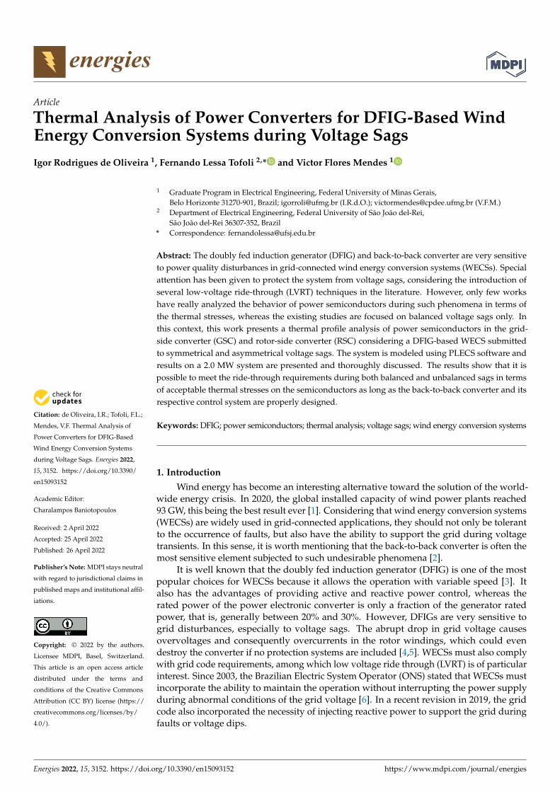
The classical control strategy uses internal loops for controlling the grid currents, whichare oriented according to the grid voltage angle. This orientation allows the decoupledcontrol of active and reactive powers [34]. The DC-link voltage control loop is external tothe control loop associated with the direct (d) axis current component, because this latterquantity is responsible for regulating the active power. The reactive power is regulated bya controller external to the loop associated with the quadrature (q) axis current component.A block diagram representation of the GSC control can be seen in Figure 2.
Energies 2022, 15, 3152 5 of 21Energies 2022, 15, x FOR PEER REVIEW 5 of 22
Figure 2. Block diagram representation of the GSC control structure.
According to Figure 2, the angle of the grid voltage vector θ, which is used in the
orientation of the converter currents, is estimated using a phase-locked loop (PLL). In this
work, the dual second-order generalized integrator (DSOGI) was adopted for this pur-
pose, whereas a detailed description can be found in [35]. The GSC is responsible for keep-
ing a constant DC-link voltage, thus allowing the RSC to regulate the rotor currents as a
consequence.
Considering the orientation of the stator voltage angle in accordance with the grid
voltage, the stator active and reactive powers are calculated as [36]:
= = −3 3
2 2d d d d
ms s s s r
s
LP v i v i
L (7)
= − = +
23 3 3
2 2 2d
q qd d
s ms s s s r
s s s
v LQ v i v i
L L (8)
The stator active and reactive powers depend on the d axis and q axis components of
the rotor current, respectively. Therefore, decoupled inner current control loops associ-
ated with outer power control loops are used in the RSC as represented in Figure 3. The
gains of the PI controllers used in RSC and GSC were obtained using the pole allocation
method, as described in [37].
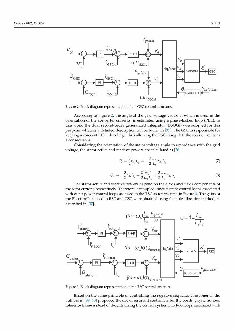
Figure 3. Block diagram representation of the RSC control structure.
Based on the same principle of controlling the negative-sequence components, the
authors in [38–40] proposed the use of resonant controllers for the positive synchronous
Figure 2. Block diagram representation of the GSC control structure.
According to Figure 2, the angle of the grid voltage vector θ, which is used in theorientation of the converter currents, is estimated using a phase-locked loop (PLL). Inthis work, the dual second-order generalized integrator (DSOGI) was adopted for thispurpose, whereas a detailed description can be found in [35]. The GSC is responsible forkeeping a constant DC-link voltage, thus allowing the RSC to regulate the rotor currents asa consequence.
Considering the orientation of the stator voltage angle in accordance with the gridvoltage, the stator active and reactive powers are calculated as [36]:
Ps =32
vsd isd = −32
Lm
Lsvsd ird (7)
Qs = −32
vsd isq =32
vsd2
ωsLs+
32
Lm
Lsvsd irq (8)
The stator active and reactive powers depend on the d axis and q axis components ofthe rotor current, respectively. Therefore, decoupled inner current control loops associatedwith outer power control loops are used in the RSC as represented in Figure 3. The gains ofthe PI controllers used in RSC and GSC were obtained using the pole allocation method, asdescribed in [37].
Energies 2022, 15, x FOR PEER REVIEW 5 of 22
Figure 2. Block diagram representation of the GSC control structure.
According to Figure 2, the angle of the grid voltage vector θ, which is used in the
orientation of the converter currents, is estimated using a phase-locked loop (PLL). In this
work, the dual second-order generalized integrator (DSOGI) was adopted for this pur-
pose, whereas a detailed description can be found in [35]. The GSC is responsible for keep-
ing a constant DC-link voltage, thus allowing the RSC to regulate the rotor currents as a
consequence.
Considering the orientation of the stator voltage angle in accordance with the grid
voltage, the stator active and reactive powers are calculated as [36]:
= = −3 3
2 2d d d d
ms s s s r
s
LP v i v i
L (7)
= − = +
23 3 3
2 2 2d
q qd d
s ms s s s r
s s s
v LQ v i v i
L L (8)
The stator active and reactive powers depend on the d axis and q axis components of
the rotor current, respectively. Therefore, decoupled inner current control loops associ-
ated with outer power control loops are used in the RSC as represented in Figure 3. The
gains of the PI controllers used in RSC and GSC were obtained using the pole allocation
method, as described in [37].
Figure 3. Block diagram representation of the RSC control structure.
Based on the same principle of controlling the negative-sequence components, the
authors in [38–40] proposed the use of resonant controllers for the positive synchronous
Figure 3. Block diagram representation of the RSC control structure.
Based on the same principle of controlling the negative-sequence components, theauthors in [38–40] proposed the use of resonant controllers for the positive synchronousreference frame instead of decentralizing the control system into two loops associated with

Energies 2022, 15, 3152 6 of 21
the positive- and negative-sequence components. This method relies on the strategy usedto mitigate harmonics in VSCs as described in [41].
The structure of the PI resonant control (PIRC) is similar to the classical controlpresented in Figures 2 and 3. The classical PI controller used in the current loops arereplaced with a PI plus resonant (PI + R) controller tuned at the twice the grid frequency,that is, the frequency of the negative-sequence component in the positive synchronousreference frame, resulting in the following transfer function:
G(s) = Kp +Kis+
sKr
s2 + (2ωs)2 (9)
where Kp is the proportional gain; Ki is the integral gain; and Kr is the resonant gain. Inorder to define the resonant gain Kr it is necessary to analyze the controller frequencyresponse as stated in [36]. The discretization method is an important issue to be consideredwhen designing the resonant controller for digital implementation purposes. Dependingon the chosen method, the resonance peak can be attenuated and the frequency can beshifted. Tustin’s method was used in this work since this is a simple and effective approach.
3. Assessment of DFIGs during Voltage Sags3.1. Balanced Voltage Sags
To carry out the theoretical analysis involving the influence of momentary voltagesags (MVSs) in DFIGs, the dynamic models of the induction machine are used, which arerepresented by Equations (1)–(4) as based on [42].
In this subsection, balanced three-phase sags are discussed, since they are the simplestphenomena that correspond to a particular case of unbalanced sags. It is assumed that thestator voltage drops instantly from its initial rated peak value Vs to a value V2 at instantt = t0:
→vs =
Vsejωst = V1ejωst, t < t0V2ejωst, t ≥ t0
(10)
where ωs is the stator angular frequencyIn DFIGs, the currents are controlled by manipulating the voltages imposed on the
rotor through the RSC. Thus, the variable of interest for the control system is the rotorvoltage, which can be obtained from Equations (2)–(4) as [42]:
→vr =
Lm
Ls
(ddt− jω
)→ψs +
[Rr + σLr
(ddt− jω
)]→ir (11)
Equation (11) represents the voltage synthetized by the RSC during the normal opera-tion. The first term of (11) is the rotor voltage portion due to the stator flux, i.e., the inducedvoltage in the rotor, whereas the second one is the portion due to the voltage drop causedby the rotor impedances.
The dynamic behavior of the stator flux expressed in terms of Equation (1) dependson the stator voltage, i.e., the grid voltage and the current that flows through the stator.Neglecting the voltage drop in the stator resistance, which is generally small, the stator fluxin steady state can be expressed as [42]:
→ψs =
Vsejωst
jωs(12)
Substituting (12) in (11) gives the rotor voltage in normal operation, that is:
→vr =
→vs
Lm
Lss +
[Rr + σLr
(ddt− jω
)]→ir (13)
where s is the machine slip. From Equation (13), it is possible to verify that generally, for alarge generator, the second term is relatively smaller than the first one because the rotor

Energies 2022, 15, 3152 7 of 21
resistance and the transient inductance (σLr) are often small. Thus, the voltage inducedon the rotor depends almost exclusively on the stator flux, which in turn depends on thestator voltage described by Equation (12).
Since the term associated with the rotor voltage drop is relatively small, a first approx-imation analyzes the behavior of the machine during an MVS considering an open-circuit
rotor, i.e.,→ir = 0. Therefore, the goal is to analyze the behavior of the voltage induced on
the rotor. Considering→ir = 0, Equations (1) and (2) lead to:
d→ψs
dt=→vs −
Rs
Ls
→ψs (14)
Before the dip at t < t0, the stator flux in steady state is totally produced by the voltageon the stator, i.e., there is only the presence of the forced system response. Thus, Equation(12) becomes:
→ψs f 1 =
V1ejωst
jωs(15)
This flux component is used as an initial condition for solving Equation (14) aimingto calculate the flux at the moment when the voltage sag occurs. Assuming that thephenomenon starts at t0 = 0, i.e., at the beginning of the sag the voltage is at the valuemaximum (worst-case condition), the stator flux response is given by [42]:
→ψs =
V2
jωsejωst +
(V1 −V2)
jωse−
tτs =
→ψs f 2 +
→ψsn (16)
where τs =LsRs
is the stator time constant;→
ψs f 2 is the forced response due to the remaining
voltage during the sag; and→
ψsn is the natural flux that induced the stator voltage transient.It is observed that the first term is constant and rotates with the synchronous frequency inthe complex plane, while the second one is a fixed vector, whose amplitude decays withthe stator time constant.
According to Equation (11), one can see that the two flux components induce voltagecomponents on the rotor. From Equation (13) and considering ir = 0, the induced voltageon the rotor caused by the forced flux yields [42]:
→v ra
r =→v r f
r +→v rn
r =Lm
Ls
(V2sejωrt −
(1τs
+ jω)
V1 −V2
jωse−
tτs e−jωt
)(17)
Analyzing Equation (17), it is observed that the first term has an amplitude and afrequency considerably lower than those of the second term. This is because the slip is lowwithin the operation range of the DFIG. The second term has a frequency equal to the rotorelectric frequency.
The worst case, i.e., when the voltage reaches the maximum value, occurs when theremaining voltage (V2) is zero and the rotating speed is as high as possible. The rotorvoltage reaches its highest value when the sag occurs and the stator voltage reaches amaximum value. In this sense, the maximum voltage appears exactly at the beginning ofthe dip. If the voltage on the stator is zero when the sag occurs, the maximum inducedvoltage will appear one-fourth cycle after the initial instant. If the stator time constant ishigh, the maximum voltage will be nearly the same in both cases. Otherwise, the secondcase will present a lower maximum voltage.
A more in-depth analysis of the DFIG behavior during balanced voltage sags can befound in [23,36], whereas the following statements are valid for balanced voltage sags:
• During balanced sags, the main problem is the natural flux component, which in-duces a high voltage on the rotor, causing high oscillatory currents that may damagethe converter;
Energies 2022, 15, 3152 8 of 21
• The natural component produces oscillations with the same frequency as that of thestator, which are reflected in the torque pulsations. This behavior is undesired fromthe point of view of the mechanical coupling between the generator and turbine;
• The natural component of the stator currents causes power oscillations in the in-jected active and reactive powers, which are undesired from the point of view of thepower system.
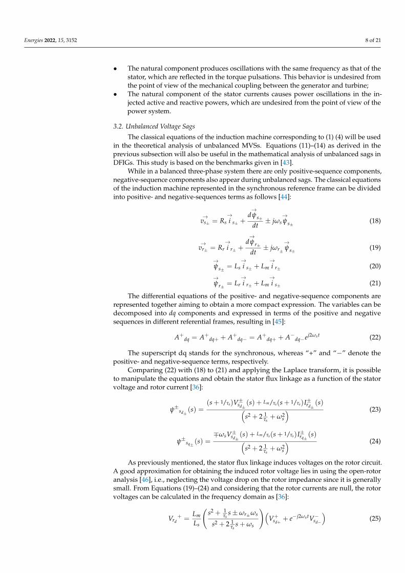
3.2. Unbalanced Voltage Sags
The classical equations of the induction machine corresponding to (1) (4) will be usedin the theoretical analysis of unbalanced MVSs. Equations (11)–(14) as derived in theprevious subsection will also be useful in the mathematical analysis of unbalanced sags inDFIGs. This study is based on the benchmarks given in [43].
While in a balanced three-phase system there are only positive-sequence components,negative-sequence components also appear during unbalanced sags. The classical equationsof the induction machine represented in the synchronous reference frame can be dividedinto positive- and negative-sequences terms as follows [44]:
→vs± = Rs
→i s± +
d→ψ s±dt± jωs
→ψ s± (18)
→vr± = Rr
→i r± +
d→ψr±dt± jωr±
→ψ s± (19)
→ψ s± = Ls
→i s± + Lm
→i r± (20)
→ψr± = Lr
→i r± + Lm
→i s± (21)
The differential equations of the positive- and negative-sequence components arerepresented together aiming to obtain a more compact expression. The variables can bedecomposed into dq components and expressed in terms of the positive and negativesequences in different referential frames, resulting in [45]:
A+dq = A+
dq+ + A+dq− = A+
dq+ + A−dq−ej2ωst (22)
The superscript dq stands for the synchronous, whereas “+” and “−” denote thepositive- and negative-sequence terms, respectively.
Comparing (22) with (18) to (21) and applying the Laplace transform, it is possibleto manipulate the equations and obtain the stator flux linkage as a function of the statorvoltage and rotor current [36]:
ψ±sd±(s) =
(s + 1/τs)V±sd±(s) + Lm/τs(s + 1/τs)I±rd±
(s)(s2 + 2 1
τs+ ω2
s
) (23)
ψ±sq± (s) =∓ωsV±sd±
(s) + Lm/τs(s + 1/τs)I±rq±(s)(
s2 + 2 1τs+ ω2
s
) (24)
As previously mentioned, the stator flux linkage induces voltages on the rotor circuit.A good approximation for obtaining the induced rotor voltage lies in using the open-rotoranalysis [46], i.e., neglecting the voltage drop on the rotor impedance since it is generallysmall. From Equations (19)–(24) and considering that the rotor currents are null, the rotorvoltages can be calculated in the frequency domain as [36]:
Vrd+ =
Lm
Ls
(s2 + 1
τss±ωr±ωs
s2 + 2 1τs
s + ωs
)(V+
sd++ e−j2ωstV−sd−
)(25)

Energies 2022, 15, 3152 9 of 21
V+rq =
Lm
Ls
((ωr± ∓ωs)s± ωr±/τs
s2 + 2 1τs
s + ωs
)(V+
sd++ e−j2ωstV−sd−
)(26)
Equations (25) and (26) show that the induced rotor voltage depends on the positive-and negative-sequence components of the d axis stator voltage. In the synchronous referenceframe, the positive-sequence term induces a constant component on the rotor voltage,whereas the negative-sequence term leads to an oscillatory component at 2ωs. If the voltageimbalance is considerable, the negative-sequence component of the rotor voltage is muchhigher than the positive-sequence one. Depending on the control action, this voltage maycause high rotor currents and damage the converter.
A more in-depth analysis of the DFIG behavior submitted to unbalanced sags can befound in [36], whereas the main statements for unbalanced voltage sags are:
• During unbalanced sags, the negative-sequence component of the rotor voltage is themain cause of excessive rotor overcurrents.
• While the natural flux component decays, the negative sequence is present during allthe sags with its amplitude dependent only on the unbalance.
• In the unbalanced case, the problem is even worse when there is also the presence ofthe natural component, since the overcurrents are caused by the sum of natural- andnegative-sequence components.
• Electromagnetic torque and grid powers will oscillate with twice the grid frequencyand higher amplitudes due to the natural- and negative-sequence components.
4. Thermal Modeling
The WECS described in Section 2 was implemented and analyzed using PLECSsoftware and considering the specifications given in Table 1.
Table 1. Specifications of the simulated system [36].
Parameter Value
GSC voltage 380 VGrid frequency 60 Hz
Rated output power 2.0 MWDC-link voltage 698 V
Switching frequency 3 kHzStator voltage 690 VStator current 1414.20 A
Stator resistance 0.002381 ΩStator leakage inductance 0.07579 mH
Rotor voltage 1380 VRotor current 707.10 A
Rotor resistance 0.002381 ΩRotor leakage inductance 0.060481 mHMagnetizing inductance 0.0023 HStator/rotor turns ratio 0.5
Inertia moment 59.47 kg/m2
Friction coefficient 0.007 N·m·sNumber of pole pairs 2
Since many manufacturers recommend a module capable of supporting a voltagearound 60% of the DC-link voltage, IGBT power modules rated at a blocking voltage of1200 V were chosen. The module should also support the maximum current produced inthe machine rotor. Therefore, module FF1500R12IE5 by Infineon, whose ratings are givenin [47], was used in the tests.
This module has a current capacity higher than the rated current of the machine rotor.Therefore, in theory, using a single module per phase would be enough for ensuring thesafe operation under normal conditions. However, the system was scaled up considering

Energies 2022, 15, 3152 10 of 21
two modules arranged in parallel so that it can operate properly even when subjectedto severe voltage sags. This association also aims to avoid the overheating of IGBTs andbody diodes. Although the GSC has a lower maximum current than the RSC, the samemodule designed for the RSC is employed in the analysis. Considering that the GSC is farless sensitive to disturbances caused by voltage sags, a preliminary analysis carried outby the authors showed that there is no need for paralleling the modules to ensure the safeoperation under both normal and sag conditions.
Using data obtained from the semiconductor datasheet, software PLECS is capableof generating the very same characteristic curves provided by manufacturers as shown inFigures 4 and 5.
Energies 2022, 15, x FOR PEER REVIEW 10 of 22
Stator current 1414.20 A
Stator resistance 0.002381 Ω
Stator leakage inductance 0.07579 mH
Rotor voltage 1380 V
Rotor current 707.10 A
Rotor resistance 0.002381 Ω
Rotor leakage inductance 0.060481 mH
Magnetizing inductance 0.0023 H
Stator/rotor turns ratio 0.5
Inertia moment 59.47 kg/m²
Friction coefficient 0.007 Nms
Number of pole pairs 2
Since many manufacturers recommend a module capable of supporting a voltage
around 60% of the DC-link voltage, IGBT power modules rated at a blocking voltage of
1200 V were chosen. The module should also support the maximum current produced in
the machine rotor. Therefore, module FF1500R12IE5 by Infineon, whose ratings are given
in [47], was used in the tests.
This module has a current capacity higher than the rated current of the machine rotor.
Therefore, in theory, using a single module per phase would be enough for ensuring the
safe operation under normal conditions. However, the system was scaled up considering
two modules arranged in parallel so that it can operate properly even when subjected to
severe voltage sags. This association also aims to avoid the overheating of IGBTs and body
diodes. Although the GSC has a lower maximum current than the RSC, the same module
designed for the RSC is employed in the analysis. Considering that the GSC is far less
sensitive to disturbances caused by voltage sags, a preliminary analysis carried out by the
authors showed that there is no need for paralleling the modules to ensure the safe oper-
ation under both normal and sag conditions.
Using data obtained from the semiconductor datasheet, software PLECS is capable
of generating the very same characteristic curves provided by manufacturers as shown in
Figures 4 and 5.
Figure 4. Turn-on losses represented in PLECS thermal library. Figure 4. Turn-on losses represented in PLECS thermal library.
Energies 2022, 15, x FOR PEER REVIEW 11 of 22
Figure 5. Characteristic curves generated in PLECS thermal library.
Power semiconductor manufacturers usually assess the thermal impedance inside
the power module, whereas the values are provided in terms of a multi-layer Foster struc-
ture as listed in Table 2.
Table 2. Junction-to-case thermal impedance of power module FF1500R12IE5.
Component Parameter 1st 2nd 3rd 4th
IGBT R (K/kW) 0.527 8.61 8.74 1.63
τ (s) 0.0012 0.0271 0.0739 0.967
Diode R (K/kW) 2.72 13.4 16.5 2.35
τ (s) 0.0012 0.0221 0.0782 1.53
Based on the semiconductor parameters, as well as using calculations and linear in-
terpolations, the software can calculate the power losses and thus estimate the junction
temperatures of semiconductor devices.
In this work, a commercial heatsink that supports two modules well spaced from
each other was considered for obtaining a more uniform thermal distribution. After an
extensive search carried out by the authors, model P16/300 by SEMIKRON was adopted
[48]. Thus, considering a heatsink of 300 mm with two IGBT modules, a thermal resistance
of 0.0024 K/W was determined from the simulation tests. It is worth mentioning that the
heatsink thermal capacitance was neglected, since the thermal loading of interest is the
one of the power semiconductors.
5. Results and Discussion
5.1. Balanced Voltage Sags
In order to understand the behavior of the DFIG-based WECS during voltage sags,
the system specified in Table 1 was analyzed in PLECS environment. The provided anal-
ysis refers always to the beginning of the dip, since this moment is generally the worst-
case condition. In the first test, the system was submitted to a balanced three-phase volt-
age sag of 20%, whereas the generator operates at the supersynchronous speed (2340 rpm)
and rated power (2.0 MW).
The stator and rotor currents are presented in Figure 6a,b, respectively. The variables
of main interest are the rotor currents, because the voltages induced on the rotor cause
overcurrents that may damage the converter. When the sag occurs, it is observed that the
rotor current peak reaches almost four times the current under normal conditions. This
peak is due to the voltage induced by the natural flux at the moment of the transient.
Analyzing the waveforms, two components can be easily identified: a low-frequency com-
ponent due to the forced rotor voltage that remains throughout the dip and a higher
Figure 5. Characteristic curves generated in PLECS thermal library.
Power semiconductor manufacturers usually assess the thermal impedance inside thepower module, whereas the values are provided in terms of a multi-layer Foster structureas listed in Table 2.
Table 2. Junction-to-case thermal impedance of power module FF1500R12IE5.
Component Parameter 1st 2nd 3rd 4th
IGBTR (K/kW) 0.527 8.61 8.74 1.63
τ (s) 0.0012 0.0271 0.0739 0.967
DiodeR (K/kW) 2.72 13.4 16.5 2.35
τ (s) 0.0012 0.0221 0.0782 1.53

Energies 2022, 15, 3152 11 of 21
Based on the semiconductor parameters, as well as using calculations and linearinterpolations, the software can calculate the power losses and thus estimate the junctiontemperatures of semiconductor devices.
In this work, a commercial heatsink that supports two modules well spaced from eachother was considered for obtaining a more uniform thermal distribution. After an exten-sive search carried out by the authors, model P16/300 by SEMIKRON was adopted [48].Thus, considering a heatsink of 300 mm with two IGBT modules, a thermal resistance of0.0024 K/W was determined from the simulation tests. It is worth mentioning that theheatsink thermal capacitance was neglected, since the thermal loading of interest is the oneof the power semiconductors.
5. Results and Discussion5.1. Balanced Voltage Sags
In order to understand the behavior of the DFIG-based WECS during voltage sags, thesystem specified in Table 1 was analyzed in PLECS environment. The provided analysisrefers always to the beginning of the dip, since this moment is generally the worst-casecondition. In the first test, the system was submitted to a balanced three-phase voltage sagof 20%, whereas the generator operates at the supersynchronous speed (2340 rpm) andrated power (2.0 MW).
The stator and rotor currents are presented in Figure 6a,b, respectively. The variablesof main interest are the rotor currents, because the voltages induced on the rotor causeovercurrents that may damage the converter. When the sag occurs, it is observed that therotor current peak reaches almost four times the current under normal conditions. This peakis due to the voltage induced by the natural flux at the moment of the transient. Analyzingthe waveforms, two components can be easily identified: a low-frequency componentdue to the forced rotor voltage that remains throughout the dip and a higher frequencycomponent due to the voltage induced by the natural flux. It is observed that this latterportion remains for the nearly the whole sag, while decaying its amplitude.
Energies 2022, 15, x FOR PEER REVIEW 12 of 22
frequency component due to the voltage induced by the natural flux. It is observed that
this latter portion remains for the nearly the whole sag, while decaying its amplitude.
(a) (b)
Figure 6. Currents during a balanced voltage sag: (a) stator currents and (b) rotor currents.
The natural component is also reflected in the powers flowing through the different
circuits as shown in Figure 7. The oscillation in the power generated by the system is un-
desired, as it degrades the grid power quality. The measured quantities are negative, de-
noting the power injection into the grid. During the sag, the powers decrease as a conse-
quence of the grid voltage reduction and the average current limitation imposed by the
power converter.
Figure 7. Active powers during a balanced voltage sag.
The rotor current oscillations also reflect on the GSC currents and DC-link voltage.
From Figure 8, one can see that at the beginning of the sag the DC-link voltage tends to
increase because of the high rotor currents flowing to the capacitors. Therefore, the GSC
direct current (active power) increases in Figure 9 to keep the DC-link voltage constant.
Nevertheless, owing to the converter current limitation and the fast transient, the DC-link
voltage tends to increase and, in order to avoid damaging the converter, a brake chopper
is used to limit the DC-link voltage at a maximum value of 733 V.
Figure 6. Currents during a balanced voltage sag: (a) stator currents and (b) rotor currents.
The natural component is also reflected in the powers flowing through the differentcircuits as shown in Figure 7. The oscillation in the power generated by the system isundesired, as it degrades the grid power quality. The measured quantities are negative,denoting the power injection into the grid. During the sag, the powers decrease as aconsequence of the grid voltage reduction and the average current limitation imposed bythe power converter.

Energies 2022, 15, 3152 12 of 21
Energies 2022, 15, x FOR PEER REVIEW 12 of 22
frequency component due to the voltage induced by the natural flux. It is observed that
this latter portion remains for the nearly the whole sag, while decaying its amplitude.
(a) (b)
Figure 6. Currents during a balanced voltage sag: (a) stator currents and (b) rotor currents.
The natural component is also reflected in the powers flowing through the different
circuits as shown in Figure 7. The oscillation in the power generated by the system is un-
desired, as it degrades the grid power quality. The measured quantities are negative, de-
noting the power injection into the grid. During the sag, the powers decrease as a conse-
quence of the grid voltage reduction and the average current limitation imposed by the
power converter.
Figure 7. Active powers during a balanced voltage sag.
The rotor current oscillations also reflect on the GSC currents and DC-link voltage.
From Figure 8, one can see that at the beginning of the sag the DC-link voltage tends to
increase because of the high rotor currents flowing to the capacitors. Therefore, the GSC
direct current (active power) increases in Figure 9 to keep the DC-link voltage constant.
Nevertheless, owing to the converter current limitation and the fast transient, the DC-link
voltage tends to increase and, in order to avoid damaging the converter, a brake chopper
is used to limit the DC-link voltage at a maximum value of 733 V.
Figure 7. Active powers during a balanced voltage sag.
The rotor current oscillations also reflect on the GSC currents and DC-link voltage.From Figure 8, one can see that at the beginning of the sag the DC-link voltage tends toincrease because of the high rotor currents flowing to the capacitors. Therefore, the GSCdirect current (active power) increases in Figure 9 to keep the DC-link voltage constant.Nevertheless, owing to the converter current limitation and the fast transient, the DC-linkvoltage tends to increase and, in order to avoid damaging the converter, a brake chopper isused to limit the DC-link voltage at a maximum value of 733 V.
Energies 2022, 15, x FOR PEER REVIEW 13 of 22
Figure 8. DC-link voltage during a balanced voltage sag.
Figure 10 shows the d and q axis components of the currents in the RSC, which sud-
denly increase at the beginning of the dip due to the natural component in the rotor volt-
age. The natural component occurs in the form of a 60 Hz oscillation in the synchronous
reference frame. However, the reference signal remains at the maximum value established
by the RSC control loops, (1500 A). In turn, the transient due to the natural component
causes the currents to reach values much higher than the rated value.
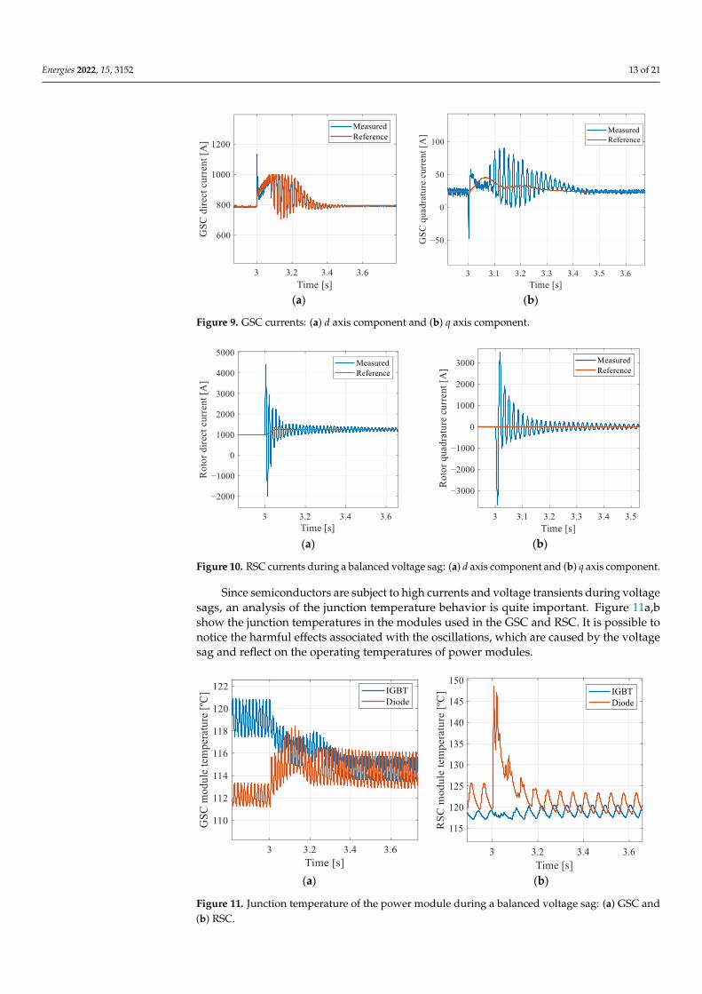
Since semiconductors are subject to high currents and voltage transients during volt-
age sags, an analysis of the junction temperature behavior is quite important. Figure 11a,b
show the junction temperatures in the modules used in the GSC and RSC. It is possible to
notice the harmful effects associated with the oscillations, which are caused by the voltage
sag and reflect on the operating temperatures of power modules.
(a) (b)
Figure 9. GSC currents: (a) d axis component and (b) q axis component.
Figure 8. DC-link voltage during a balanced voltage sag.
Figure 10 shows the d and q axis components of the currents in the RSC, whichsuddenly increase at the beginning of the dip due to the natural component in the rotorvoltage. The natural component occurs in the form of a 60 Hz oscillation in the synchronousreference frame. However, the reference signal remains at the maximum value establishedby the RSC control loops, (1500 A). In turn, the transient due to the natural componentcauses the currents to reach values much higher than the rated value.
Energies 2022, 15, 3152 13 of 21
Energies 2022, 15, x FOR PEER REVIEW 13 of 22
Figure 8. DC-link voltage during a balanced voltage sag.
Figure 10 shows the d and q axis components of the currents in the RSC, which sud-
denly increase at the beginning of the dip due to the natural component in the rotor volt-
age. The natural component occurs in the form of a 60 Hz oscillation in the synchronous
reference frame. However, the reference signal remains at the maximum value established
by the RSC control loops, (1500 A). In turn, the transient due to the natural component
causes the currents to reach values much higher than the rated value.
Since semiconductors are subject to high currents and voltage transients during volt-
age sags, an analysis of the junction temperature behavior is quite important. Figure 11a,b
show the junction temperatures in the modules used in the GSC and RSC. It is possible to
notice the harmful effects associated with the oscillations, which are caused by the voltage
sag and reflect on the operating temperatures of power modules.
(a) (b)
Figure 9. GSC currents: (a) d axis component and (b) q axis component. Figure 9. GSC currents: (a) d axis component and (b) q axis component.
Energies 2022, 15, x FOR PEER REVIEW 14 of 22
(a) (b)
Figure 10. RSC currents during a balanced voltage sag: (a) d axis component and (b) q axis compo-
nent.
(a) (b)
Figure 11. Junction temperature of the power module during a balanced voltage sag: (a) GSC and
(b) RSC.
The behavior of the power modules used in GSC and RSC are slightly different under
normal operating conditions. The thermal stress is higher for the IGBTs and body diodes
in the GSC and RSC, respectively. This is because the power flows from the AC side to the
DC one in the RSC, whereas the power flow direction is opposite in the GSC. In particular,
Figure 11a shows that there is an increase in the diode junction temperature at the begin-
ning of the sag, caused by the spikes that occur in both the DC-link voltage and GSC cur-
rents.
It is worth noting that the RSC is the most affected element, since the natural compo-
nent causes overcurrents in the rotor, resulting in spikes in the junction temperature of
the semiconductor devices according to Figure 11b. It is also observed that the thermal
cycling for the components of the power modules in the RSC is lower than for that in the
GSC. In other words, the devices are exposed to higher temperatures for a longer time.
This is because the currents in the RSC have a lower frequency (approximately 18 Hz)
than that of the GSC (60 Hz).
It is important to highlight that the junction temperatures of the semiconductor de-
vices did not exceed the limit that power module supports, that is, a maximum of 175 °C.
Therefore, the thermal design ensures the safe operation of the system, even when sub-
jected to severe balanced voltage sags. This is a consequence of the design conditions
adopted in this study, thus evidencing that it is necessary to increase the current capacity
of the power converter to meet grid code requirements.
Figure 10. RSC currents during a balanced voltage sag: (a) d axis component and (b) q axis component.
Since semiconductors are subject to high currents and voltage transients during voltagesags, an analysis of the junction temperature behavior is quite important. Figure 11a,bshow the junction temperatures in the modules used in the GSC and RSC. It is possible tonotice the harmful effects associated with the oscillations, which are caused by the voltagesag and reflect on the operating temperatures of power modules.
Energies 2022, 15, x FOR PEER REVIEW 14 of 22
(a) (b)
Figure 10. RSC currents during a balanced voltage sag: (a) d axis component and (b) q axis compo-
nent.
(a) (b)
Figure 11. Junction temperature of the power module during a balanced voltage sag: (a) GSC and
(b) RSC.
The behavior of the power modules used in GSC and RSC are slightly different under
normal operating conditions. The thermal stress is higher for the IGBTs and body diodes
in the GSC and RSC, respectively. This is because the power flows from the AC side to the
DC one in the RSC, whereas the power flow direction is opposite in the GSC. In particular,
Figure 11a shows that there is an increase in the diode junction temperature at the begin-
ning of the sag, caused by the spikes that occur in both the DC-link voltage and GSC cur-
rents.
It is worth noting that the RSC is the most affected element, since the natural compo-
nent causes overcurrents in the rotor, resulting in spikes in the junction temperature of
the semiconductor devices according to Figure 11b. It is also observed that the thermal
cycling for the components of the power modules in the RSC is lower than for that in the
GSC. In other words, the devices are exposed to higher temperatures for a longer time.
This is because the currents in the RSC have a lower frequency (approximately 18 Hz)
than that of the GSC (60 Hz).
It is important to highlight that the junction temperatures of the semiconductor de-
vices did not exceed the limit that power module supports, that is, a maximum of 175 °C.
Therefore, the thermal design ensures the safe operation of the system, even when sub-
jected to severe balanced voltage sags. This is a consequence of the design conditions
adopted in this study, thus evidencing that it is necessary to increase the current capacity
of the power converter to meet grid code requirements.
Figure 11. Junction temperature of the power module during a balanced voltage sag: (a) GSC and(b) RSC.

Energies 2022, 15, 3152 14 of 21
The behavior of the power modules used in GSC and RSC are slightly different undernormal operating conditions. The thermal stress is higher for the IGBTs and body diodes inthe GSC and RSC, respectively. This is because the power flows from the AC side to theDC one in the RSC, whereas the power flow direction is opposite in the GSC. In particular,Figure 11a shows that there is an increase in the diode junction temperature at the beginningof the sag, caused by the spikes that occur in both the DC-link voltage and GSC currents.
It is worth noting that the RSC is the most affected element, since the natural compo-nent causes overcurrents in the rotor, resulting in spikes in the junction temperature of thesemiconductor devices according to Figure 11b. It is also observed that the thermal cyclingfor the components of the power modules in the RSC is lower than for that in the GSC.In other words, the devices are exposed to higher temperatures for a longer time. This isbecause the currents in the RSC have a lower frequency (approximately 18 Hz) than that ofthe GSC (60 Hz).
It is important to highlight that the junction temperatures of the semiconductor devicesdid not exceed the limit that power module supports, that is, a maximum of 175 C.Therefore, the thermal design ensures the safe operation of the system, even when subjectedto severe balanced voltage sags. This is a consequence of the design conditions adopted inthis study, thus evidencing that it is necessary to increase the current capacity of the powerconverter to meet grid code requirements.
5.2. Unbalanced Voltage Sags
In this section, the behavior of the WECS when submitted to an unbalanced voltagesag of 20% is assessed in terms of relevant variables. The instant at which the phenomenonoccurs was defined in such a way that the highest natural component is induced. This testwas performed at supersynchronous speed (2340 rpm) and rated power (2.0 MW).
The stator and rotor currents are presented in Figure 12a,b, respectively. In addition tothe natural component, there is the presence of the negative-sequence component, whichcauses oscillations at a frequency equal to twice the stator frequency (120 Hz). Similarly tothe balanced case, it is possible to observe the presence of high current peaks caused bythe natural component in the stator and rotor, reaching almost five times the rated value.However, compared with the balanced case, the peak caused by the natural component ineither condition is not so different. In turn, the current values during the sag are higher forthe unbalanced condition, since there is the influence of the negative-sequence component.
Energies 2022, 15, x FOR PEER REVIEW 15 of 22
5.2. Unbalanced Voltage Sags
In this section, the behavior of the WECS when submitted to an unbalanced voltage
sag of 20% is assessed in terms of relevant variables. The instant at which the phenomenon
occurs was defined in such a way that the highest natural component is induced. This test
was performed at supersynchronous speed (2340 rpm) and rated power (2.0 MW).
The stator and rotor currents are presented in Figure 12a,b, respectively. In addition
to the natural component, there is the presence of the negative-sequence component,
which causes oscillations at a frequency equal to twice the stator frequency (120 Hz). Sim-
ilarly to the balanced case, it is possible to observe the presence of high current peaks
caused by the natural component in the stator and rotor, reaching almost five times the
rated value. However, compared with the balanced case, the peak caused by the natural
component in either condition is not so different. In turn, the current values during the
sag are higher for the unbalanced condition, since there is the influence of the negative-
sequence component.
(a) (b)
Figure 12. DFIG currents for an unbalanced voltage sag of 20%: (a) stator currents and (b) rotor
currents.
The negative-sequence component also causes oscillations in the stator power as seen
in Figure 13. Such oscillations are undesirable and may further contribute to the degrada-
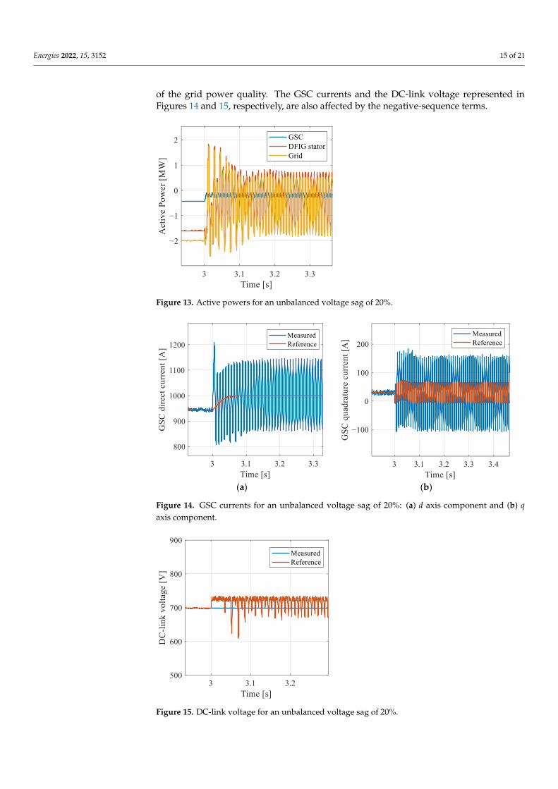
tion of the grid power quality. The GSC currents and the DC-link voltage represented in
Figures 14 and 15, respectively, are also affected by the negative-sequence terms.
Figure 13. Active powers for an unbalanced voltage sag of 20%.
Figure 12. DFIG currents for an unbalanced voltage sag of 20%: (a) stator currents and(b) rotor currents.
The negative-sequence component also causes oscillations in the stator power as seenin Figure 13. Such oscillations are undesirable and may further contribute to the degradation
Energies 2022, 15, 3152 15 of 21
of the grid power quality. The GSC currents and the DC-link voltage represented inFigures 14 and 15, respectively, are also affected by the negative-sequence terms.
Energies 2022, 15, x FOR PEER REVIEW 15 of 22
5.2. Unbalanced Voltage Sags
In this section, the behavior of the WECS when submitted to an unbalanced voltage
sag of 20% is assessed in terms of relevant variables. The instant at which the phenomenon
occurs was defined in such a way that the highest natural component is induced. This test
was performed at supersynchronous speed (2340 rpm) and rated power (2.0 MW).
The stator and rotor currents are presented in Figure 12a,b, respectively. In addition
to the natural component, there is the presence of the negative-sequence component,
which causes oscillations at a frequency equal to twice the stator frequency (120 Hz). Sim-
ilarly to the balanced case, it is possible to observe the presence of high current peaks
caused by the natural component in the stator and rotor, reaching almost five times the
rated value. However, compared with the balanced case, the peak caused by the natural
component in either condition is not so different. In turn, the current values during the
sag are higher for the unbalanced condition, since there is the influence of the negative-
sequence component.
(a) (b)
Figure 12. DFIG currents for an unbalanced voltage sag of 20%: (a) stator currents and (b) rotor
currents.
The negative-sequence component also causes oscillations in the stator power as seen
in Figure 13. Such oscillations are undesirable and may further contribute to the degrada-
tion of the grid power quality. The GSC currents and the DC-link voltage represented in
Figures 14 and 15, respectively, are also affected by the negative-sequence terms.
Figure 13. Active powers for an unbalanced voltage sag of 20%. Figure 13. Active powers for an unbalanced voltage sag of 20%.
Energies 2022, 15, x FOR PEER REVIEW 16 of 22
From the rotor currents in the synchronous reference shown in Figure 16, it is possi-
ble to provide a more comprehensive analysis of the control system performance. It is
observed that the natural component decays and only the negative-sequence component
remains throughout the dip. This is because the controller saturates as a consequence of
the severity of the sag, demanding a higher voltage as shown in Figure 17. Analyzing the
rotor voltage in Figure 17, it becomes evident that the peak values of the rotor voltages at
the beginning of the sag do exceed the converter limit (400 V). Under this condition, the
RSC operates in the overmodulation region. In this particular case, the resonant controller
cannot ensure the accurate control of the rotor currents.
(a) (b)
Figure 14. GSC currents for an unbalanced voltage sag of 20%: (a) d axis component and (b) q axis
component.
Figure 15. DC-link voltage for an unbalanced voltage sag of 20%.
Figure 14. GSC currents for an unbalanced voltage sag of 20%: (a) d axis component and (b) qaxis component.
Energies 2022, 15, x FOR PEER REVIEW 16 of 22
From the rotor currents in the synchronous reference shown in Figure 16, it is possi-
ble to provide a more comprehensive analysis of the control system performance. It is
observed that the natural component decays and only the negative-sequence component
remains throughout the dip. This is because the controller saturates as a consequence of
the severity of the sag, demanding a higher voltage as shown in Figure 17. Analyzing the
rotor voltage in Figure 17, it becomes evident that the peak values of the rotor voltages at
the beginning of the sag do exceed the converter limit (400 V). Under this condition, the
RSC operates in the overmodulation region. In this particular case, the resonant controller
cannot ensure the accurate control of the rotor currents.
(a) (b)
Figure 14. GSC currents for an unbalanced voltage sag of 20%: (a) d axis component and (b) q axis
component.
Figure 15. DC-link voltage for an unbalanced voltage sag of 20%. Figure 15. DC-link voltage for an unbalanced voltage sag of 20%.

Energies 2022, 15, 3152 16 of 21
From the rotor currents in the synchronous reference shown in Figure 16, it is possibleto provide a more comprehensive analysis of the control system performance. It is observedthat the natural component decays and only the negative-sequence component remainsthroughout the dip. This is because the controller saturates as a consequence of the severityof the sag, demanding a higher voltage as shown in Figure 17. Analyzing the rotor voltagein Figure 17, it becomes evident that the peak values of the rotor voltages at the beginningof the sag do exceed the converter limit (400 V). Under this condition, the RSC operates inthe overmodulation region. In this particular case, the resonant controller cannot ensurethe accurate control of the rotor currents.
Energies 2022, 15, x FOR PEER REVIEW 17 of 22
(a) (b)
Figure 16. RSC currents for an unbalanced voltage sag of 20%: (a) d axis component and (b) q axis
component.
Figure 17. Rotor voltage in phase A for an unbalanced voltage sag of 20%.
The semiconductor devices are also subjected to oscillations caused by the negative-
sequence component. Figure 18a shows the semiconductor temperatures in the GSC. At
the beginning of the dip, there is a sudden increase in the diode temperature. Similar to
the case of the balanced sags, this is due to the increase in the GSC currents in an attempt
to keep the output power constant. The increase in the diode temperature is directly re-
lated to the increase in the GSC currents. The negative-sequence component remains
throughout the dip, as the controller saturates owing to the restriction imposed by the
converter voltage limits. Although the IGBT temperature was expected to decrease at the
beginning of the sag, similar to the balanced case, it remains almost unchanged during
the entire phenomenon. This is because the controller is ineffective in dampening the neg-
ative-sequence component that contributes to the increase in GSC currents.
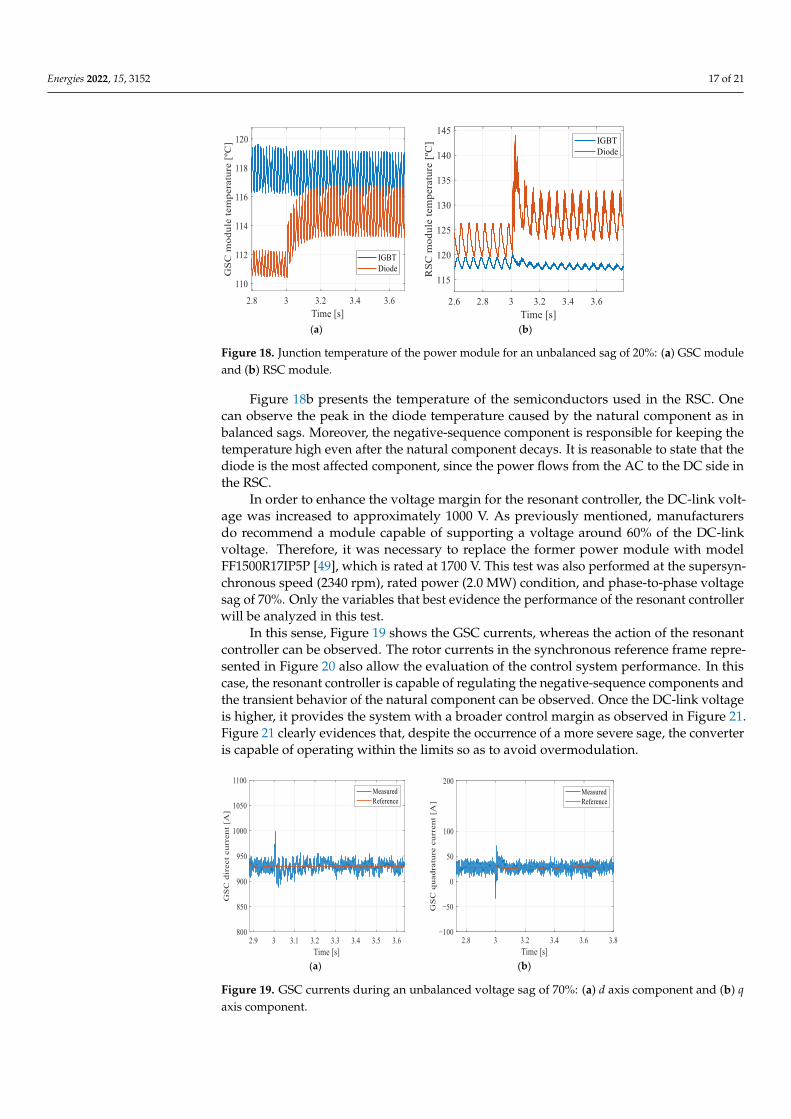
Figure 18b presents the temperature of the semiconductors used in the RSC. One can
observe the peak in the diode temperature caused by the natural component as in bal-
anced sags. Moreover, the negative-sequence component is responsible for keeping the
temperature high even after the natural component decays. It is reasonable to state that
the diode is the most affected component, since the power flows from the AC to the DC
side in the RSC.
In order to enhance the voltage margin for the resonant controller, the DC-link volt-
age was increased to approximately 1000 V. As previously mentioned, manufacturers do
recommend a module capable of supporting a voltage around 60% of the DC-link voltage.
Therefore, it was necessary to replace the former power module with model
Figure 16. RSC currents for an unbalanced voltage sag of 20%: (a) d axis component and (b) qaxis component.
Energies 2022, 15, x FOR PEER REVIEW 17 of 22
(a) (b)
Figure 16. RSC currents for an unbalanced voltage sag of 20%: (a) d axis component and (b) q axis
component.
Figure 17. Rotor voltage in phase A for an unbalanced voltage sag of 20%.
The semiconductor devices are also subjected to oscillations caused by the negative-
sequence component. Figure 18a shows the semiconductor temperatures in the GSC. At
the beginning of the dip, there is a sudden increase in the diode temperature. Similar to
the case of the balanced sags, this is due to the increase in the GSC currents in an attempt
to keep the output power constant. The increase in the diode temperature is directly re-
lated to the increase in the GSC currents. The negative-sequence component remains
throughout the dip, as the controller saturates owing to the restriction imposed by the
converter voltage limits. Although the IGBT temperature was expected to decrease at the
beginning of the sag, similar to the balanced case, it remains almost unchanged during
the entire phenomenon. This is because the controller is ineffective in dampening the neg-
ative-sequence component that contributes to the increase in GSC currents.
Figure 18b presents the temperature of the semiconductors used in the RSC. One can
observe the peak in the diode temperature caused by the natural component as in bal-
anced sags. Moreover, the negative-sequence component is responsible for keeping the
temperature high even after the natural component decays. It is reasonable to state that
the diode is the most affected component, since the power flows from the AC to the DC
side in the RSC.
In order to enhance the voltage margin for the resonant controller, the DC-link volt-
age was increased to approximately 1000 V. As previously mentioned, manufacturers do
recommend a module capable of supporting a voltage around 60% of the DC-link voltage.
Therefore, it was necessary to replace the former power module with model
Figure 17. Rotor voltage in phase A for an unbalanced voltage sag of 20%.
The semiconductor devices are also subjected to oscillations caused by the negative-sequence component. Figure 18a shows the semiconductor temperatures in the GSC. Atthe beginning of the dip, there is a sudden increase in the diode temperature. Similar to thecase of the balanced sags, this is due to the increase in the GSC currents in an attempt tokeep the output power constant. The increase in the diode temperature is directly relatedto the increase in the GSC currents. The negative-sequence component remains throughoutthe dip, as the controller saturates owing to the restriction imposed by the converter voltagelimits. Although the IGBT temperature was expected to decrease at the beginning of the sag,similar to the balanced case, it remains almost unchanged during the entire phenomenon.This is because the controller is ineffective in dampening the negative-sequence componentthat contributes to the increase in GSC currents.
Energies 2022, 15, 3152 17 of 21
Energies 2022, 15, x FOR PEER REVIEW 18 of 22
FF1500R17IP5P [49], which is rated at 1700 V. This test was also performed at the super-
synchronous speed (2340 rpm), rated power (2.0 MW) condition, and phase-to-phase volt-
age sag of 70%. Only the variables that best evidence the performance of the resonant
controller will be analyzed in this test.
(a) (b)
Figure 18. Junction temperature of the power module for an unbalanced sag of 20%: (a) GSC module
and (b) RSC module.
In this sense, Figure 19 shows the GSC currents, whereas the action of the resonant
controller can be observed. The rotor currents in the synchronous reference frame repre-
sented in Figure 20 also allow the evaluation of the control system performance. In this
case, the resonant controller is capable of regulating the negative-sequence components
and the transient behavior of the natural component can be observed. Once the DC-link
voltage is higher, it provides the system with a broader control margin as observed in
Figure 21. Figure 21 clearly evidences that, despite the occurrence of a more severe sage,
the converter is capable of operating within the limits so as to avoid overmodulation.
(a) (b)
Figure 19. GSC currents during an unbalanced voltage sag of 70%: (a) d axis component and (b) q
axis component.
Figure 22a shows the temperature of the power semiconductor module used in the
GSC. At the beginning of the sag, there is a small increase in the diode temperature. This
is because the DC-link voltage tends to increase, causing the GSC currents to increase as
Figure 18. Junction temperature of the power module for an unbalanced sag of 20%: (a) GSC moduleand (b) RSC module.
Figure 18b presents the temperature of the semiconductors used in the RSC. Onecan observe the peak in the diode temperature caused by the natural component as inbalanced sags. Moreover, the negative-sequence component is responsible for keeping thetemperature high even after the natural component decays. It is reasonable to state that thediode is the most affected component, since the power flows from the AC to the DC side inthe RSC.
In order to enhance the voltage margin for the resonant controller, the DC-link volt-age was increased to approximately 1000 V. As previously mentioned, manufacturersdo recommend a module capable of supporting a voltage around 60% of the DC-linkvoltage. Therefore, it was necessary to replace the former power module with modelFF1500R17IP5P [49], which is rated at 1700 V. This test was also performed at the supersyn-chronous speed (2340 rpm), rated power (2.0 MW) condition, and phase-to-phase voltagesag of 70%. Only the variables that best evidence the performance of the resonant controllerwill be analyzed in this test.
In this sense, Figure 19 shows the GSC currents, whereas the action of the resonantcontroller can be observed. The rotor currents in the synchronous reference frame repre-sented in Figure 20 also allow the evaluation of the control system performance. In thiscase, the resonant controller is capable of regulating the negative-sequence components andthe transient behavior of the natural component can be observed. Once the DC-link voltageis higher, it provides the system with a broader control margin as observed in Figure 21.Figure 21 clearly evidences that, despite the occurrence of a more severe sage, the converteris capable of operating within the limits so as to avoid overmodulation.
Energies 2022, 15, x FOR PEER REVIEW 18 of 22
FF1500R17IP5P [49], which is rated at 1700 V. This test was also performed at the super-
synchronous speed (2340 rpm), rated power (2.0 MW) condition, and phase-to-phase volt-
age sag of 70%. Only the variables that best evidence the performance of the resonant
controller will be analyzed in this test.
(a) (b)
Figure 18. Junction temperature of the power module for an unbalanced sag of 20%: (a) GSC module
and (b) RSC module.
In this sense, Figure 19 shows the GSC currents, whereas the action of the resonant
controller can be observed. The rotor currents in the synchronous reference frame repre-
sented in Figure 20 also allow the evaluation of the control system performance. In this
case, the resonant controller is capable of regulating the negative-sequence components
and the transient behavior of the natural component can be observed. Once the DC-link
voltage is higher, it provides the system with a broader control margin as observed in
Figure 21. Figure 21 clearly evidences that, despite the occurrence of a more severe sage,
the converter is capable of operating within the limits so as to avoid overmodulation.
(a) (b)
Figure 19. GSC currents during an unbalanced voltage sag of 70%: (a) d axis component and (b) q
axis component.
Figure 22a shows the temperature of the power semiconductor module used in the
GSC. At the beginning of the sag, there is a small increase in the diode temperature. This
is because the DC-link voltage tends to increase, causing the GSC currents to increase as
Figure 19. GSC currents during an unbalanced voltage sag of 70%: (a) d axis component and (b) qaxis component.

Energies 2022, 15, 3152 18 of 21
Energies 2022, 15, x FOR PEER REVIEW 19 of 22
a consequence in order to keep both the voltage and power constant. Figure 22b represents
the temperatures in the semiconductors of the RSC. The average temperature of the de-
vices is slightly lower due to the severity of the sage, although a further reduction in this
quantity was expected. However, it does not occur because the higher voltage thresholds
required by the control action as associated with the power converter operation do lead
to higher operating temperatures, especially in the diode. Another possible cause is that
the negative-sequence component may remain during the whole dip. Since the thermal
dynamics is slower than that of the currents, the system may still remain under the harm-
ful effects of the negative-sequence component.
(a) (b)
Figure 20. Rotor currents during an unbalanced voltage sag of 70%: (a) d axis component and (b) q
axis component.
Figure 21. Rotor voltages in phase A during an unbalanced voltage sag of 70%.
Figure 20. Rotor currents during an unbalanced voltage sag of 70%: (a) d axis component and (b) qaxis component.
Energies 2022, 15, x FOR PEER REVIEW 19 of 22
a consequence in order to keep both the voltage and power constant. Figure 22b represents
the temperatures in the semiconductors of the RSC. The average temperature of the de-
vices is slightly lower due to the severity of the sage, although a further reduction in this
quantity was expected. However, it does not occur because the higher voltage thresholds
required by the control action as associated with the power converter operation do lead
to higher operating temperatures, especially in the diode. Another possible cause is that
the negative-sequence component may remain during the whole dip. Since the thermal
dynamics is slower than that of the currents, the system may still remain under the harm-
ful effects of the negative-sequence component.
(a) (b)
Figure 20. Rotor currents during an unbalanced voltage sag of 70%: (a) d axis component and (b) q
axis component.
Figure 21. Rotor voltages in phase A during an unbalanced voltage sag of 70%. Figure 21. Rotor voltages in phase A during an unbalanced voltage sag of 70%.
Figure 22a shows the temperature of the power semiconductor module used in theGSC. At the beginning of the sag, there is a small increase in the diode temperature. This isbecause the DC-link voltage tends to increase, causing the GSC currents to increase as aconsequence in order to keep both the voltage and power constant. Figure 22b representsthe temperatures in the semiconductors of the RSC. The average temperature of the devicesis slightly lower due to the severity of the sage, although a further reduction in this quantitywas expected. However, it does not occur because the higher voltage thresholds requiredby the control action as associated with the power converter operation do lead to higheroperating temperatures, especially in the diode. Another possible cause is that the negative-sequence component may remain during the whole dip. Since the thermal dynamics isslower than that of the currents, the system may still remain under the harmful effects ofthe negative-sequence component.

Energies 2022, 15, 3152 19 of 21Energies 2022, 15, x FOR PEER REVIEW 20 of 22
(a) (b)
Figure 22. Junction temperature of the power module during an unbalanced voltage sag of 70%: (a)
GSC and (b) RSC.
6. Conclusions
This work has presented a comprehensive thermal analysis of a DFIG-based WECS.
The junction temperatures of power semiconductors were evaluated in order to verify the
thermal stress to which they are subjected. The results showed the behavior of the most
relevant variables when voltage sags occur. The analysis clearly evidences that the DFIG
is very sensitive to such power quality phenomena, considering that the oscillations in the
stator flux cause overcurrents in the rotor due to the presence of natural- and negative-
sequence components. This issue becomes more intense as the sag level increases, since
the higher the value assumed by the aforementioned components, the higher the influence
on the increase in the junction temperature of semiconductors. Therefore, it is reasonable
to state that the thermal profile of power semiconductors is of major importance for de-
signing the system while ensuring its safe operation during such phenomena.
The PI + R controller adopted in the study proved to be quite effective in reducing
the negative-sequence component, which is not high during the sag so as to avoid the
excessive increase in the operating temperature of power semiconductors. In turn, other
studies have shown that this strategy may become more effective if the voltage capability
of the converter is increased, thus providing the control system with a wider margin.
Thus, it is necessary to choose IGBTs rated at higher voltages, thus increasing the overall
cost.
Future work includes the analysis of LVRT strategies from the point of view of ther-
mal stresses on semiconductors. This analysis aims to determine the best solutions for
protecting the DFIG under such severe conditions. The whole study is supposed to be
validated using a laboratory setup comprising a small-scale WECS.
Author Contributions: Conceptualization, V.F.M.; methodology, V.F.M.; validation, I.R.d.O.; for-
mal analysis, I.R.d.O.; investigation, I.R.d.O.; writing—original draft preparation, I.R.d.O.; writ-
ing—review and editing, F.L.T. and V.F.M.; supervision, F.L.T. and V.F.M. All authors have read
and agreed to the published version of the manuscript.
Funding: This research was funded by the Coordenação de Aperfeiçoamento de Pessoal de Nível
Superior–Brazil (CAPES)–Finance Code 001. The authors would also like to acknowledge Conselho
Nacional de Desenvolvimento Científico e Tecnológico (CNPq)—Project 436213/2018-4; Fundação
de Amparo à Pesquisa do Estado de Minas Gerais (FAPEMIG)—Project APQ-01187-18; and Instituto
Nacional de Ciência e Tecnologia em Energia Elétrica (INERGE) for supporting this work.
Institutional Review Board Statement: Not applicable.
Informed Consent Statement: Not applicable.
Data Availability Statement: Data available on request from the authors.
Figure 22. Junction temperature of the power module during an unbalanced voltage sag of 70%:(a) GSC and (b) RSC.
6. Conclusions
This work has presented a comprehensive thermal analysis of a DFIG-based WECS.The junction temperatures of power semiconductors were evaluated in order to verify thethermal stress to which they are subjected. The results showed the behavior of the mostrelevant variables when voltage sags occur. The analysis clearly evidences that the DFIG isvery sensitive to such power quality phenomena, considering that the oscillations in thestator flux cause overcurrents in the rotor due to the presence of natural- and negative-sequence components. This issue becomes more intense as the sag level increases, since thehigher the value assumed by the aforementioned components, the higher the influence onthe increase in the junction temperature of semiconductors. Therefore, it is reasonable tostate that the thermal profile of power semiconductors is of major importance for designingthe system while ensuring its safe operation during such phenomena.
The PI + R controller adopted in the study proved to be quite effective in reducing thenegative-sequence component, which is not high during the sag so as to avoid the excessiveincrease in the operating temperature of power semiconductors. In turn, other studieshave shown that this strategy may become more effective if the voltage capability of theconverter is increased, thus providing the control system with a wider margin. Thus, it isnecessary to choose IGBTs rated at higher voltages, thus increasing the overall cost.
Future work includes the analysis of LVRT strategies from the point of view of thermalstresses on semiconductors. This analysis aims to determine the best solutions for protectingthe DFIG under such severe conditions. The whole study is supposed to be validated usinga laboratory setup comprising a small-scale WECS.
Author Contributions: Conceptualization, V.F.M.; methodology, V.F.M.; validation, I.R.d.O.; formalanalysis, I.R.d.O.; investigation, I.R.d.O.; writing—original draft preparation, I.R.d.O.; writing—review and editing, F.L.T. and V.F.M.; supervision, F.L.T. and V.F.M. All authors have read and agreedto the published version of the manuscript.
Funding: This research was funded by the Coordenação de Aperfeiçoamento de Pessoal de NívelSuperior–Brazil (CAPES)–Finance Code 001. The authors would also like to acknowledge ConselhoNacional de Desenvolvimento Científico e Tecnológico (CNPq)—Project 436213/2018-4; Fundação deAmparo à Pesquisa do Estado de Minas Gerais (FAPEMIG)—Project APQ-01187-18; and InstitutoNacional de Ciência e Tecnologia em Energia Elétrica (INERGE) for supporting this work.
Institutional Review Board Statement: Not applicable.
Informed Consent Statement: Not applicable.
Data Availability Statement: Data available on request from the authors.
Conflicts of Interest: The authors declare no conflict of interest.
Energies 2022, 15, 3152 20 of 21
References1. Global Wind Energy Council. Global Wind Report 2021; Global Wind Energy Council: Brussels, Belgium, 2021.2. Shen, Y.; Zhang, B.; Liang, L.; Cui, T. A novel control strategy for enhancing the LVRT and voltage support capabilities of DFIG.
In IOP Conference Series: Earth and Environmental Science; IOP Publishing: Bristol, UK, 2018; Volume 121, p. 042035.3. Saeed, M.A.; Khan, H.M.; Ashraf, A.; Qureshi, S.A. Analyzing effectiveness of LVRT techniques for DFIG wind turbine system
and implementation of hybrid combination with control schemes. Renew. Sustain. Energy Rev. 2018, 81, 2487–2501. [CrossRef]4. Xiang, D.; Ran, L.; Tavner, P.J.; Yang, S. Control of a doubly fed induction generator in a wind turbine during grid fault
ride-through. IEEE Trans. Energy Convers. 2006, 21, 652–662. [CrossRef]5. Yang, L.; Xu, Z.; Ostergaard, J.; Dong, Z.Y.; Wong, K.P. Advanced control strategy of DFIG wind turbines for power system fault
ride through. IEEE Trans. Power Syst. 2011, 27, 713–722. [CrossRef]6. ONS. Procedimentos de Rede—Submódulo 3.6: Requisitos Técnicos Mínimos Para a Conexão à Rede Básica; ONS: Rio de Janeiro, Brazil, 2009.7. Justo, J.; Bansal, R. Parallel R-L configuration crowbar with series R-L circuit protection for LVRT strategy of DFIG under
transient-state. Electr. Power Syst. Res. 2018, 154, 299–310. [CrossRef]8. Naderi, S.B.; Negnevitsky, M.; Muttaqi, K.M. A modified DC chopper for limiting the fault current and controlling the DC-link
voltage to enhance fault ride-through capability of doubly-fed induction-generator-based wind turbine. IEEE Trans. Ind. Appl.2018, 55, 2021–2032. [CrossRef]
9. Gray, C.; Buque, C.; Chowdhury, S. AC series dynamic resistor protection scheme with switching control for doubly fed inductiongenerator based WECS. In Proceedings of the 2016 IEEE Power and Energy Society General Meeting (PESGM), Boston, MA, USA,17–21 July 2016; pp. 1–5.
10. Kim, J.; Muljadi, E.; Gevorgian, V.; Hoke, A.F. Dynamic capabilities of an energy storage-embedded DFIG system. IEEE Trans. Ind.Appl. 2019, 55, 4124–4134. [CrossRef]
11. Huang, J.; Zhang, L.; Sang, S.; Xue, X.; Zhang, X.; Sun, T.; Wu, W.; Gao, N. Optimized series dynamic braking resistor for LVRT ofdoubly-fed induction generator with uncertain fault scenarios. IEEE Access 2022, 10, 22533–22546. [CrossRef]
12. Liang, J.; Qiao, W.; Harley, R.G. Feed-forward transient current control for low-voltage ride-through enhancement of DFIG windturbines. IEEE Trans. Energy Convers. 2010, 25, 836–843. [CrossRef]
13. Zhu, D.; Zou, X.; Deng, L.; Huang, Q.; Zhou, S.; Kang, Y. Inductance-emulating control for DFIG-based wind turbine toride-through grid faults. IEEE Trans. Power Electron. 2016, 32, 8514–8525. [CrossRef]
14. Zhu, D.; Zou, X.; Zhou, S.; Dong, W.; Kang, Y.; Hu, J. Feedforward current references control for DFIG-based wind turbine toimprove transient control performance during grid faults. IEEE Trans. Energy Convers. 2017, 33, 670–681. [CrossRef]
15. Liang, J.; Howard, D.F.; Restrepo, J.A.; Harley, R.G. Feedforward transient compensation control for DFIG wind turbines duringboth balanced and unbalanced grid disturbances. IEEE Trans. Ind. Appl. 2013, 49, 1452–1463. [CrossRef]
16. Liu, R.; Yao, J.; Wang, X.; Sun, P.; Pei, J.; Hu, J. Dynamic stability analysis and improved LVRT schemes of DFIG-based windturbines during a symmetrical fault in a weak grid. IEEE Trans. Power Electron. 2019, 35, 303–318. [CrossRef]
17. Ruiz-Cruz, R.; Sanchez, E.N.; Loukianov, A.G.; Ruz-Hernandez, J.A. Real-time neural inverse optimal control for a wind generator.IEEE Trans. Sustain. Energy 2018, 10, 1172–1183. [CrossRef]
18. Ozsoy, E.; Padmanaban, S.; Mihet-Popa, L.; Fedák, V.; Ahmad, F.; Akhtar, R.; Sabanovic, A. Control strategy for a grid-connectedinverter under unbalanced network conditions—A disturbance observer-based decoupled current approach. Energies 2017, 10, 1067.[CrossRef]
19. Kong, X.; Wang, X.; Abdelbaky, M.A.; Liu, X.; Lee, K.Y. Nonlinear MPC for DFIG-based wind power generation under unbalancedgrid conditions. Int. J. Electr. Power Energy Syst. 2022, 134, 107416. [CrossRef]
20. Xiong, L.; Li, P.; Wang, J. High-order sliding mode control of DFIG under unbalanced grid voltage conditions. Int. J. Electr. PowerEnergy Syst. 2020, 117, 105608. [CrossRef]
21. Rafiee, Z.; Heydari, R.; Rafiee, M.; Aghamohammadi, M.R.; Blaabjerg, F. Enhancement of the LVRT capability for DFIG-basedwind farms based on short-circuit capacity. IEEE Syst. J. 2022, 1–12. [CrossRef]
22. Hiremath, R.; Moger, T. Modified Super Twisting algorithm based sliding mode control for LVRT enhancement of DFIG drivenwind system. Energy Reports 2022, 8, 3600–3613. [CrossRef]
23. Mendes, V.F.; de Sousa, C.V.; Silva, S.; Rabelo, B.C.; Hofmann, W. Modeling and ride-through control of doubly fed inductiongenerators during symmetrical voltage sags. IEEE Trans. Energy Convers. 2011, 26, 1161–1171. [CrossRef]
24. Zhou, L.; Liu, J.; Zhou, S. Improved demagnetization control of a doubly-fed induction generator under balanced grid fault. IEEETrans. Power Electron. 2014, 30, 6695–6705. [CrossRef]
25. Blaabjerg, F.; Chen, Z.; Kjaer, S.B. Power electronics as efficient interface in dispersed power generation systems. IEEE Trans.Power Electron. 2004, 19, 1184–1194. [CrossRef]
26. Blaabjerg, F.; Ma, K.; Zhou, D. Power electronics and reliability in renewable energy systems. In Proceedings of the 2012 IEEEInternational Symposium on Industrial Electronics, Hangzhou, China, 28–31 May 2012; pp. 19–30.
27. Zhou, D.; Blaabjerg, F. Thermal analysis of two-level wind power converter under symmetrical grid fault. In Proceedings ofthe IECON 2013-39th Annual Conference of the IEEE Industrial Electronics Society, Vienna, Austria, 10–13 November 2013; pp.1904–1909.
Energies 2022, 15, 3152 21 of 21
28. Zhou, D.; Blaabjerg, F.; Lau, M.; Tonnes, M. Thermal behavior of doubly-fed induction generator wind turbine system duringbalanced grid fault. In Proceedings of the 2014 IEEE Applied Power Electronics Conference and Exposition-APEC 2014, FortWorth, TX, USA, 16–20 March 2014; pp. 3076–3083.
29. Wintrich, A.; Nicolai, U.; Tursky, W.; Reimann, T. Application Manual—Power Semiconductors; Semikron International GmbH:Nuremberg, Germany, 2011.
30. Behjati, H.; Davoudi, A. Reliability analysis framework for structural redundancy in power semiconductors. IEEE Trans. Ind.Electron. 2013, 10, 4376–4386. [CrossRef]
31. Musarrat, M.N.; Islam, M.R.; Muttaqi, K.; Sutanto, D.; Rahman, M.A. Improving the thermal performance of rotor-side converterof doubly-fed induction generator wind turbine while operating around synchronous speed. IEEE J. Emerg. Sel. Top. Ind. Electron.2021, 3, 298–307. [CrossRef]
32. Zhou, D.; Blaabjerg, F. Optimized demagnetizing control of DFIG power converter for reduced thermal stress during symmetricalgrid fault. IEEE Trans. Power Electron. 2018, 33, 10326–10340. [CrossRef]
33. Kovács, P.K. Transient Phenomena in Electrical Machines; Elsevier: Amsterdam, The Netherlands, 1984.34. Pena, R.; Clare, J.; Asher, G. Doubly fed induction generator using back-to-back PWM converters and its application to variable-
speed wind-energy generation. IEE Proc.-Electr. Power Appl. 1996, 143, 231–241. [CrossRef]35. Rodriguez, P.; Teodorescu, R.; Candela, I.; Timbus, A.V.; Liserre, M.; Blaabjerg, F. New positive-sequence voltage detector for
grid synchronization of power converters under faulty grid conditions. In Proceedings of the 2006 37th IEEE Power ElectronicsSpecialists Conference, Jeju, Korea, 18–22 June 2006; pp. 1–7.
36. Mendes, V.F.; de Sousa, C.V.; Hofmann, W.; Silva, S.R. Doubly-fed induction generator ride-through fault capability usingresonant controllers for asymmetrical voltage sags. IET Renew. Power Gener. 2015, 9, 783–791. [CrossRef]
37. Teodorescu, R.; Liserre, M.; Rodriguez, P. Grid Converters for Photovoltaic and Wind Power Systems; John Wiley & Sons: Hoboken,NJ, USA, 2011.
38. Hu, J.; He, Y. Modeling and enhanced control of DFIG under unbalanced grid voltage conditions. Electr. Power Syst. Res. 2009, 79,273–281. [CrossRef]
39. Hu, J.; He, Y.; Xu, L.; Williams, B.W. Improved control of DFIG systems during network unbalance using PI–R current regulators.IEEE Trans. Ind. Electron. 2008, 56, 439–451. [CrossRef]
40. Hu, J.; He, Y. DFIG wind generation systems operating with limited converter rating considered under unbalanced networkconditions–analysis and control design. Renew. Energy 2011, 36, 829–847. [CrossRef]
41. Liserre, M.; Teodorescu, R.; Blaabjerg, F. Multiple harmonics control for three-phase grid converter systems with the use of PI-REScurrent controller in a rotating frame. IEEE Trans. Power Electron. 2006, 21, 836–841. [CrossRef]
42. Lopez, J.; Sanchis, P.; Roboam, X.; Marroyo, L. Dynamic behavior of the doubly fed induction generator during three-phasevoltage dips. IEEE Trans. Energy Convers. 2007, 22, 709–717. [CrossRef]
43. López, J.; Sanchis, P.; Gubía, E.; Ursúa, A.; Marroyo, L.; Roboam, X. Control of doubly fed induction generator under symmetricalvoltage dips. In Proceedings of the 2008 IEEE International Symposium on Industrial Electronics, Cambridge, UK, 30 June–2 July2008; pp. 2456–2462.
44. Bollen, M.H. Understanding Power Quality Problems; IEEE Press: Piscataway, NJ, USA, 2000.45. Xu, L. Coordinated control of DFIG’s rotor and grid side converters during network unbalance. IEEE Trans. Power Electron. 2008,
23, 1041–1049.46. Lopez, J.; Gubia, E.; Sanchis, P.; Roboam, X.; Marroyo, L. Wind turbines based on doubly fed induction generator under
asymmetrical voltage dips. IEEE Trans. Energy Convers. 2008, 23, 321–330. [CrossRef]47. Infineon Datasheet of Module FF1500R12IE5. Available online: https://www.infineon.com/dgdl/Infineon-FF1500R12IE5
-DataSheet-v03_01-EN.pdf?fileId=5546d4625f2e26bc015f2e9197d90007 (accessed on 20 April 2022).48. SEMIKRON Datasheet of Heatsink P16/300. Available online: https://pdf1.alldatasheetpt.com/datasheet-pdf/view/127115
/SEMIKRON/P16/300.html (accessed on 20 April 2022).49. Infineon Datasheet of Module FF1500R17IP5P. Available online: https://www.infineon.com/dgdl/Infineon-FF1500R17IP5P-
DataSheet-v03_02-EN.pdf?fileId=5546d46264a8de7e0164f4b761db4512 (accessed on 20 April 2022).
Related Documents