"HEORY AND APPLICATIONS ^^ FIELD-L""7~^CT TPJ\NSlf""70"\ r by /&? COE WILLAP.D TOLIVER 3. S., Prairie View as: College, 1952 A MASTER'S REPORT sv-bnitted in partial fulfillment of requirements for the FAST"?. 0? SCIENCE Department of Electrical Engineering KANSAS STATS UNIVE"^T '" Manhattan, Kansas 19S7 Approved by: 2 Major Professor i /

Theory and Application of Field Effect Transistors
Nov 27, 2015
1962 thesis on field effect transistors
Welcome message from author
This document is posted to help you gain knowledge. Please leave a comment to let me know what you think about it! Share it to your friends and learn new things together.
Transcript

"HEORY AND APPLICATIONS ^^ FIELD-L""7~^CT TPJ\NSlf""70"\r
by /&?
COE WILLAP.D TOLIVER
3. S., Prairie View as: College, 1952
A MASTER'S REPORT
sv-bnitted in partial fulfillment of
requirements for the
FAST"?. 0? SCIENCE
Department of Electrical Engineering
KANSAS STATS UNIVE"^T '"
Manhattan, Kansas
19S7
Approved by:
]
2
Major Professori
/

LU
Hi "
CONTENTS
Page
INTRODUCTION 1
CONSTRUCTION OF FIELD-EFFECT TRANSISTORS 4
THE FIELD-EFFECT TRANSISTOR 7
FIELD-EFFECT TRANSISTOR THEORY 10
The Conductive Channel 11
Depletion Layer Potential 13
Channel Current 17
Characteristics of Field-effect Transistors 21
Mutual Transconductance 22
Determining the Field-effect TransistorPinch-off Voltage 26
Temperature Dependence of I 2 8
BIASING FIELD-EFFECT TRANSISTORS 30
SELECTING THE 3S~T FIELD-EFFECT TRANSISTOR 36
tCUIT DESIGN 3 8
SMALL-SIGNAL LOW FREQUENCY-PROPERTIES 41
SMALL-SIGNAL EQUIVALENT CIRCUIT 45
FIELD EFFECT TRANSISTOR AMPLIFIERS 49
Basic FET Amplifier Configurations 49
Voltage Amplifier Circuit 50
The Source-follov;er Circuit 51
FET Cascade with 3ipolar Transistor 53
THE POWER FIELD-EFFECT TRANSISTOR 59
CONCLUSIONS 61

Ill
Page
REFERENCES 64
ACKNOWLEDGEMENT 66
LIST OF PRINCIPAL SYMBOLS 67
INTRODUCTION
In 1952, shortly after the invention of the junction
transistor, Shockley (18) described theoretically a new active
device based on the modulation of a majority-carrier current.
The principle of operation of this device, which he termed a
unipolar field-effect transistor, is radically different from
that of the junction transistor in that the majority - rather
than minority-carrier current is modulated by altering the
width of a conducting channel through the narrowing or widen-
ing of a p-n junction depletion layer. At that time, probably
the principle attraction of this device over the junction
transistor was the high input impedance of the control elec-
trode, which behaves essentially as a reverse-biased p-n
junction. However, the difficulties of making the device with
the techniques then available were considerable, and, although
both silicon and germanium (7) devices were described shortly
after Shockley 's papor was published, the device in its prac-
tical form did not appear very attractive. It was not until
the techniques of masking, diffusion and epitaxial growth
using silicon were sufficiently developed that field-effect
devices could be manufactured with a reasonable degree of
reproducibility and with characteristics which offered con-
siderable advantages over the junction transistor for certain
applications. In fact, it is only in the last few years that
the devices have become readily available through commercial
channels
.
The theory of the device, as originally formulated by
Shockley, can be considered as a first-order theory. It
assumed an abrupt p-n junction with a uniformly graded
channel along which the change in potential is gradual
enough to allow the use of the charge-neutrality condition.
Furthermore, Shockley assumed that the carrier mobility was
independent of the electric field. Dacey and Ross (7) modi-
fied this theory to include the effects of variable mobility.
In addition, they considered in some detail the high-frequency
performance of the device. By comparison with experimental
measurements on transistors constructed by the alloy process,
they showed that the general features of the d-c character-
istics of some units were adequately explained by the first-
order theory of Shockley, while for others some modified
theory was necessary.
Modern field-effect transistors (FET) are constructed
by methods which result in junctions of both the abrupt and
graded types. Recently there has been renewed interest in the
solid-state field in both the conventional junction field-effect
transistor and in the more recently developed surface or metal-
oxide-semiconductor (MOS) device.
While the details of carrier motion and control are
different for the several types of field-effect devices, basic
equations describing all types of devices have the same
mathematical form and can thus be treated in a unified approach.
The purpose of this report is to discuss and solve a gener-

alized model of an abrupt junction field-effect transistor
by developing the basic relations among its parameters. An
attempt is also made to present its most important features
as an active device by including device application.

CONSTRUCTION OF FIELD-EFFECT TRANSISTORS
In order to compare the performance of a practical field-
effect transistor with theoretical predictions, it is necessary
to assume a suitable structural model. Such a model and an
assessment of its validity can be best obtained by considering
the methods by which the devices are made.
The techniques of alloying, diffusion and epitaxial growth,
or combinations thereof, can be used for device fabrication.
This discussion will be restricted to the diffusion processes,
since it and the epitaxial process enable the best control over
impurity density and dimensions to be obtained.
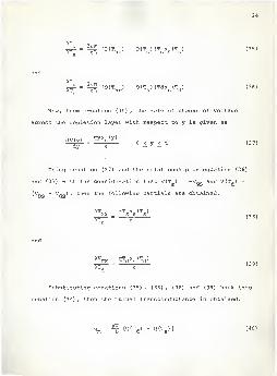
The structure illustrated in Fig. 1 can be achieved by using
double-diffusion techniques similar to those employed in making
silicon n-p-n transistors. Either simultaneous or sequential
double diffusion can be used. If sequential diffusion is employed,
a suitable acceptor impurity is first diffused into an n-type
silicon slice, producing a p-type layer. A "photoresist" pro-
cedure is then used to produce a silicon-oxide mask over all the
surface, except where it is desired to produce a channel. Dif-
fusion of donor impurities then converts the selected region of
the p-layer into an n-type gate, the depth of which is controlled
by the diffusion time and temperature. The doping profile that
may be expected to result from such a procedure is shown in Fig.
2.
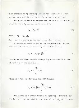
Another technique (15) which can yield field-effect tran-
sistors with a high transconductance and cutoff frequency

Dram
Channel Gate * 2 V X Y2
Fig. 1. Construction of a double-diffusedtransistor. The p channel is formed by dif-fusing acceptors into the n substrate, whichforms the second gate. A second diffusionthrough the masked surface forms gate 1.
log|ND-NA |
Gate 1 Gate 2
log|ND-NA |
Fig. 2. Approximate form of the doping profilefor the double-diffused structure shown in Fig. 1.Net impurity density: a Along y. ; b Along y_
.
utilizes the fact that diffusion can occur laterally beneath a
masked area to produce a channel region. The junctions of this
structure are diffused, and it might be expected that, since both
gate regions are of the same resistivity, this device should ex-
hibit symmetrical gate characteristics (9)
.

THE FIELD-EFFECT TRANSISTOR
Illustrated in Fig. 3 is an example of a junction gate
field-effect transistor. It is shown to be a three terminal de-
vice formed by introducing two n-type impurities into opposite
sides of the p-type material. The two n-type regions are shown
to be electrically connected and form the gate (grid) terminal.
The interesting part of the field-effect transistor is the region
between the two junctions which is called the conductive channel.
The conductive channel is provided with two ohmic contacts, one
acting as the source (cathode) and the other as the drain (anode)
with an appropriate voltage (drain voltage) applied between drain
and source terminals. If the impurity concentration in the n-
regions is purposely made much higher than that of the p-region,
then a space-charge layer due to the external bias V__ will ex-GG
tend almost entirely into the channel between junctions, thus
controlling the thickness of the channel. If the bias potential
at the source and drain differ, then under operating conditions
there will be a narrowing of the channel at the terminal that has
the larger potential.
In a field-effect transistor, the current flow is carried
by one type of carrier only. The changed conductance of the
field-effect transistor input and output terminals results from
changing numbers of carriers of this one type. For this reason
the field-effect transistor is some times refered to as a "uni-
polar transistor".

It is perhaps well to point out at this point that the field-
effect transistor of Fig. 3 is in some ways analogous to a vacuum
tube. Suppose that it be imagined that a small time varying sig-
nal is applied between source and gate terminals, then the effect
will be to widen and narrow the channel which carries current be-
tween source and drain terminals. This is closely analogous to
the action of a grid which controls the current flow between
cathode and plate.
If in Fig. 3 the impurities diffuse through the p-region in
a plane parallel to the n-regions, then the conductance of the
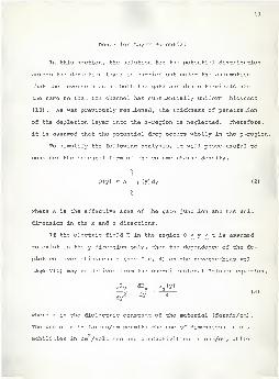
channel can be calculated from the following expression:
Fig. 3. The field-effect transistor.
= ^ p(y)dy (1)

where p = the impurity density in the p-region (N - N )
.
q = the electronic charge,
u = carrier drift mobility.
Referring to equation (1) , it is seen that the conductance
between source and drain terminals depends on the effective
channel thickness T . The effective channel thickness is en-
tirely determined by the region between p-n junctions not de-
pleted of free carriers by the reverse bias junction gate voltage.
Thus, it is easy to see how the applied voltage Vr controls the
conductance of the semiconductor body.
10
FIELD-EFFECT TRANSISTOR THEORY
A mathematical representation of field-effect transistors
provides a basis for predicting transistor performance and the
influence of various design and material parameters. Published
analyses (18) and (7) have been limited to specific device geo-
metries and impurity distributions.
The solutions of the field-effect transistor equations
presented here are general in that both the free carrier density
and space-charge density may vary arbitrarily with distance from
the gate junction (1) . However the solutions are limited to
cases where the one dimensional Poisson-equations can be employed
in rectangular form. The gradual approximation originated by
Shockley (18) is employed. Solutions based on this approximation
have been shown to agree favorably with experimental results (7)
.
Many of the relationships derived here have been previously noted
in analyses of specific impurity distributions. However, this re-
port will show that many of these relationships are independent
of distribution.
The amplifying properties of a field-effect transistor are
best characterized by its mutual transconductance . Both mutual
transconductance and output current approach constant maximum
values (g and I ) when the output terminal voltage reaches a
particular value V . The value of V also represents the magni-
tude of the input terminal voltage required to reduce the output
current to zero. In the following sections general expressions
for mutual transconductance, output transconductance, junction
11
capacitance, and current amplification are derived as functions
of the depletion layer thickness at the device boundaries. These
expressions are not explicitly dependent on charge distribution
(1).
The Conductive Channel
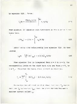
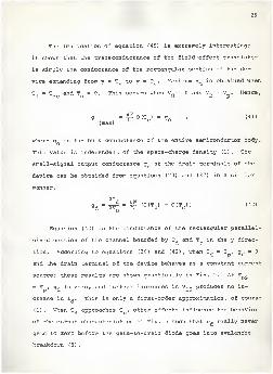
The physical structure for this analysis is illustrated in
Fig. 4. Note that only the lower half p-n junction of the field-
effect transistor of Fig. 3 is shown. Also, only the active
channel is shown in Fig. 4., and it has length L, width W, and
thickness T, . T, is the half channel thickness,he he
In Fig. 4, the space-charge region is represented as lying
entirely in the p-region. This is only an approximation; but it
is a good one (18) since the impurities in the n-region are much
greater than that of the p-region. The lower surface (gate)
represents a junction boundary. When this junction is reverse
biased a depletion layer forms which extends a distance t into
the channel. The value of t depends on the reverse bias voltage
and increases with distance x in as much as the potential in the
conducting channel increases with that distance when a drain
current I, is flowing (18) . A current I, between source and
drain contacts results when a voltage V„ is applied between the
source and drain terminals. This current is restricted to the
region beneath the depletion layer boundary. A field-effect
transistor may have either an n-type channel or a p-type channel.
From a circuit point of view, the structures are the same except
12
that the terminal voltages and currents are of opposite polarities.
In Fig. 4 all voltages are measured with respect to the source
terminal. The values of T and T. are the extent of the depletions a
layer at the source and drain respectively.
Fig. 4. The active channel of thefield-effect transistor.
Free carriers constitute a mobile charge density in the
region above the depletion layer boundary. Although a one-to-one
correspondence usually exists between free and space-charge densi-
ties, certain exceptions occur (2). Therefore free and space-
charge densities are represented independently by p (y) and p-(y),
(coul/cm ) in order to maintain the generality of this analysis
(1) .
13
Depletion Layer Potential
In this section, the solution for the potential distribution
across the depletion layer is carried out under the assumption
that the reverse bias at both the gate and drain terminals are
the same so that the channel has substantially uniform thickness
(18). As was previously mentioned, the thickness of penetration
of the depletion layer into the n-region is neglected. Therefore,
it is assumed that the potential drop occurs wholly in the p-region.
To simplify the following analysis, it will prove useful to
consider the integral form of the volume charge density.
fQ(y) = A p(y)dy (2)
where A is the effective area of the gate junction and has unit
dimension in the x and z directions.
If the electric field E in the region <_ y < t is assumed
to exist in the y direction only, then the dependence of the de-
pletion layer thickness t (see Fig. 4) on the reverse-bias vol-
tage V(t) may be derived from the one-dimensional Poisson equation.
where c is the dielectric constant of the material (farads/cm)
.
The use of e in farads/cm permits the use of dimensions in cm,
2mobilities in cm /volt sec and conductivities in ohm/cm, while

14
retaining currents and voltages in amp and volt. Also p (y)
(space-charge density) ; p = impurity density (N - N )
.
Integration of equation (3) yields
qp
E =y
Ps(y)dy + C
1(4)
Near y = t there is an abrupt transistion region at which
p (y) is zero. Consequently, it is assumed that at the edge of
the depletion layer E =0. Thus using the boundary condition
to evaluate the constant of integration yields
Ps(y)dy (5)
therefore
Pg(y)dy - - p
g(y)dy (6)
When equation (2) is substituted into equation (6) then
Ey
=f-
[Q(y) - Q(t)] (7)
The voltage across the depletion layer can now be obtained
by integrating equation (7) between < y < t.

15
V(t) = - i [Q(y) - Q(t)] dy (8)
Hence
,
V(t) = | [yQ(t) -I
The terms in the brackets of equation (9) are an integral of a
product and can be expressed as
V(t) = i yps(y) dy (10)
Therefore the voltage across the depletion layer as a
function of t is given by equation (10)
.
Equation (10) has an important limit in the form of a pinch-
off voltage V when the upper limit of integration is allowed to
go to T. . Remembering that advantage of the symmetry of the field-
effect transistor has been taken, this limit then yields the re-
verse bias voltage that removes all the free charge from the con-
ducting channel; thus the current path has been pinched-off i.e.,
the channel no longer has the ability to conduct current. The
pinch-off voltage V is defined then as the magnitude of the in-
put gate voltage, V , required to reduce the output current toG
zero. Hence,

16
, r.c
',-* y » s (y) dy (11)
i
The junction capacitance of the field-effect transistor can
now oe evaluated. The differential of equation (10) is
dV(y) = | (ycs(y)dy) o < y < t (12)
When equation (2) is substituted into equation (12) , equation
(12) becomes
dV(y) _ 2ydQ(y)Ac
< y < t (13)
where
dQ(y) = Aps(y)dy (14)
therefore
,
dVL
_ eAj 2t (y = t) (15)
Equation (15) del ines the junction capacitance and shows
that the space-charge layer thus acts as a parallel plate cap a-
citor with plate separation t.
1

17
Channel Current
An expression relating the drain current, I, to the physical
Darameters of the transistor and to the applied voltages can be
derived from Ohm's law. When a current flows in the plus x di-
rection in the channel of Fig. 4, an electric field with a com-
ponent Exmust be present. This requires that the potential
changes along the channel. Since the gate terminals carry no
current they are equipotentials . Hence the reverse voltage be-
tween channel and the n-regions varies with distance x and there-
fore the channel thickness varies (18). In the previous section,
the derivation of the relationship between depletion layer thick-
ness t and reverse-bias voltage V assumed that
3x
so that a one-dimensional Poission equation could be used. How-
ever when current flows
,
Ex = I * ° < C17)
in general —=• will not vanish. However, if —y is very small3x 3x
compared to p (y)/e, then the one dimensional approximation can
be used for channel potential V(y) and the reverse bias channel
potential V(x) will be the same as in the case of I , » (18)
.
The approximation that V(x) and t(x) change gradually with distance
18
x is referred to by Shockley (18) as the gradual case. The
gradual case will be assumed in the following discussion.
Ohm's law in terms of current density in the x direction J ,
electric field E and conductivity a(x) is
Jx
= Ex<j(x) (18)
where c(x) = qp f (y)y-
Now P^(y) qp- (y) is the free space charge density.
Substituting these relations and the expression for the
electric field from equation (17) into equation (18)
,
Jx= " PfW i < 19)
from which the total current through any cross section of the
channel can be obrained i.e.,
he
1=2x
JxdS (20)
where dS = Wdy, so that equation (20) becomes
T,he
Ix
= 2y ^ W I pf(y)
The factor of 2 occurs because of symmetry. Equation (21)
can be simplified somewhat by replacing dV by — yp (y) dy as given
19
by equation (12). Hence,
T2Wuyp„(y) dy f
Ixdx = 5 P
f(y)cty (22)
t
From equation (2) assuming unit dimensions in the x and z direc-
tions then,
/he
Q(Thc ) - Q(t) = P
f(y)dy (23)
J
t
Substituting this relationship into equation (22) , it then
becomes
Ixdx =
^f- tQ(Thc ) - Q(t)]yos(y)dy (24)
When equation (24) is integrated from x = to x = L , the
corresponding limits on the right-hand side are from y = T to
y = T, . Therefore the total drain current is given by,
V* _ 2 "Wxd eL
[Q(Thc ) - Q(t)]yos(y)dy (25)
Ts
An examination of equation (25) shows that when T equals
zero and T, approaches T. , then the drain current becomes a
maximum current called I .
P

20
From equation (25) it is quite apparent that the current is
a function of the space-charge layer heights at both the source
and drain ends of the .channel which in turn are functions of the
voltages across the depletion layer at each end of the channel:
i .e.
Ts
= F(VGS ) (26)
Td " G[V
DS " VGS ] (27)
At this point it is convenient to define I , as the drain
current that flows when the external gate and source terminals
are shorted together. By this definition, I is the drain cur-
rent for any value of voltage between source and drain V„ , but
will be restricted to the current that flows when V „ has a value
that causes T, to equal T. (5) . That value of voltage was shown
to be V in the previous section. Hence,P
Tjhc
I = 4t^ [Q< tJ - Q<t)]yp (y)dy (28)
This is abnormal of course, since if T, equals T, , the
conducting channel thickness is zero and no current can flow. Or
what is more likely, if the conducting channel thickness goes to
zero, then the current density must go to infinity, since when
V„ = it is not possible to cause I to go to zero by increasing
V_„. The answer to this dilemma is that T, cannot equal T. ,DS d he
21
because there is a fundamental limit on how narrow the conducting
channel can be (1) . If the limiting value of the current density
is J , then I = WJ AT. where AT, is the narrowest possiblemax p max he he
conducting channel. Equation (2 8) is therefore only an approxi-
mation. The real upper' limit on the integral is (Thc
- ATh ) ,
but the approximation given is a good one because Thc is much
greater than AThc (5) .
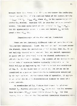
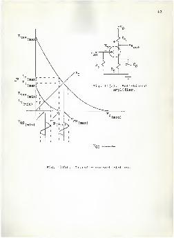
Characteristics of the Field-Effect Transistor
There are two distinctly different modes of operation of the
field-effect transistor. First, for zero or small voltages across
the channel, where the conductance of the channel (see Fig. 5) is
not markedly changed by the current flow, and second, operation
in pinch-off (or saturation) where the channel conductance is
affected by the flow of current. The current of the device in this
latter mode of operation becomes virtually independent of the
drain voltage as depicted by the device's output characteristics
of Fig. 5. In the first mode of operation, the device can be
considered as a passive element-variable conductance controlled
by the gate voltage. In the second mode of operation, it appears
as an active device with characteristics similar to those of a
vacuum pentode.
An examination of Fig. 5 shows that beyond the pinch-off
voltage V , further increases in VDS
(up to the junction reverse-
bias breakdown, BV___) causes little change in I,. For this
reason, this portion of the field-effect transistor characteristics
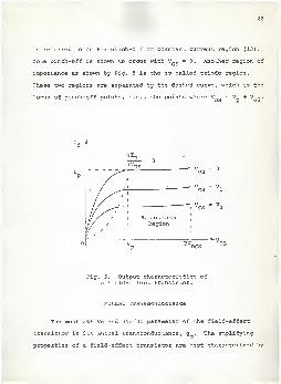
22
is referred to as the pinch-off or constant current region (13).
Note pinch-off is shown to occur with Vr„ = 0. Another region of
importance as shown by Fig. 5 is the so called triode region.
These two regions are separated by the dashed curve, which is the
locus of pinch-off points, i.e., the points where Vnc,= V + V
s.
DS
Fig. 5. Output characteristics ofa field-effect transistor.
Mutual Transconductance
The most active and useful parameter of the field-effect
transistor is its mutual transconductance, g . The amplifying
properties of a field-effect transistor are best characterized by

t. j
its mutua 1 trans conductance. It has been Pr '3viously shown that
the drain current is a function of the small increments of gate-
to- source voltage and the drain-to-source vo ltage, i .e. ,
I = f 'VGS<
V0S>
(29)
Equation (29) can be written as
AId
3Id
3Id= - AV + —
3VQ
AVG 3V
DAV
D(30)
the re fore
AId = VV
G+
^dAV
D(31)
whe re
?m=
3ID
3VG
(32)
and
<?d"
3VD
(33)
so that
<?m=
3Id
3Id
3Ts .
3VG
" 3TS
3VG
9Id
3Td
3TD
3VG
(34)
3'."" JI,
The partial der•ivatives ~ and j£"s d
can be evaluated from
equation (25) Thus /
and
24
S^^l! tQ(Thc ) - Q(Tg)]T
g0s(T
s) (35)
s
St-^E t° (Thc'
-Q(Ts)]Tdp
s(Td ) (36)
a
Now, from equation (10) , the rate of change of voltage
across the depletion layer with respect to y is given as
dvfv) qyo„(y)
Using equation (37) and the relationship in equation (26)
and (27) with the consideration that V(T ) = -V_„ and V(T.) =s GS a
(V _ - V__) , then the following partials are obtained.
W~ E(38)
S
and
3Vgs qVs'V nq ,
3Td
Substituting eauations (35), (36), (38) and (39) back into
equation (34) , then the mutual transconductance is obtained.
%- 3 k<V " Q(Ts>
] < 40 >
25
The implication of equation (40) is extremely interesting;
it shows that the transconductance of the field-effect transistor
is simply the conductance of the rectangular section of the de-
vice extending from y = T to y = T,. Maximum g is obtained when
T, = T, and T =0. This occurs when V_ = and V_ = V. Hence,d he s G D p
*m, =^ Q(Tc>=9o •< 41 >
(max)
where g is the bulk conductance of the entire semiconductor body.o
This value is independent of the space-charge density (1) . The
small-signal output conductance g, at the drain terminals of the
device can be obtained from equations (23) and (37) in a similar
manner.
*d = ^ = ir »<V " Q(Td" (42 >
Equation (42) is the conductance of the rectangular parallel-
piped portion of the channel bounded by T, and T in the y direc-
tion. According to equations (28) and (42) , when I, = I , g . =
and the drain terminal of the device behaves as a constant-current
source; these results are shown graphically in Pig. 5. At V _
" V , g, is zero, and further increases in V„ produces no in-p ^d DS
crease in I.. This is only a first-order approximation, of course
(1) . When T, approaches T , other effects influence the behavior
of the output characteristics of Pig. 5 such that g, really never
gets to zero before the gate-to-drain diode goes into avalanche
breakdown (5) .
26
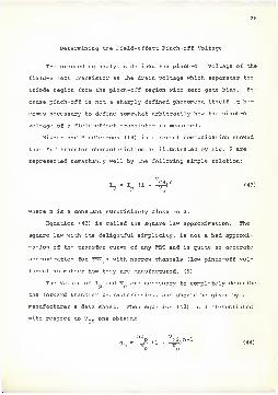
Determining the Field-effect Pinch-off Voltage
The preceeding analysis defined the pinch-off voltage of the
field-effect transistor as the drain voltage which separates the
triode region from the pinch-off region with zero gate bias. Be-
cause pinch-off is not a sharply defined phenomena itself it be-
comes necessary to define somewhat arbitrarily how the pinch-off
voltage of a field-effect transistor is measured.
Richer and Middlebrook (14) in a recent communication showed
that FET transfer characteristics as illustrated by Fig. 6 are
represented remarkably well by the following simple relation;
JD - *p (1 " ¥>" (43)
*P
where n is a constant surprisingly close to 2.
Equation (43) is called the square law approximation. The
square law with its delightful simplicity, is not a bad approxi-
mation of the transfer curve of any FET and is quite an accurate
approximation for FET ' s with narrow channels (low pinch-off vol-
tages) no matter how they are manufactured. (6)
The values of I and V are necessary to completely describe
the forward transfer characteristics, and should be given by a
manufacturer's data sheet. When equation (43) is differentiated
with respect to V _ one obtains
nl V„ _ .
^m=^E < 1 -T) < 44)
P P
27
DSS
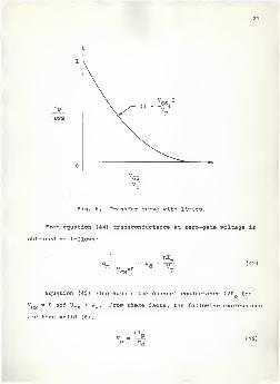
Fig. 6. Transfer curve with limits.
From equation (44) trans conductance at zero-gate voltage is
obtained as follows:
1VGS=°
nly d V
P(45)
Equation (45) also equals the channel conductance 1/R for
VGS
= and V„ < V . From these facts, the following expressions
are then valid (6)
.
nlv -•—
E
p gd(46)
28
V = nl R (47)P P °
Both of these equations give V a fairly precise meaning.
The terms on the right hand side of equation (45) are measured in
the pinch-off region and for all practical purposes are indepen-
dent of the drain voltage. Equation (46) has the advantage that
V is obtained quite simply from the static output characteristics.
In either case the value obtained for V by these methods character-
ize the field-effect transistor in a broader sense than a value
obtained in the usual manner (6) . These equations developed above
have shown that all field-effect transistors have a fixed relation-
ship between pinch-off voltage V , zero-bias current I , and zero-
bias forward transconductance . Thus it is possible, given a sin-
gle set of reference values, to determine specific parameter
values for a select device.
What has been said indicates that when making calculations
for the design of field-effect transistor circuits, I and V
give most of the information necessary. Other FET characteristics
(except for breakdown voltages) can be regarded as causing only
second-order effects; for the most part they can be ignored (6).
Temperature Dependence of I
Although I is not greatly dependent on the drain-to-source
voltage as was pointed out in its derivation, it is a very strong
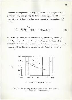
29
function of temperature as Fig. 7 attests. The temperature de-
pendence of I can quickly be derived from equation (28) . Dif-
ferentiation of this equation with respect to temperature (T )
yields
dl2W du
A,rhc
dTA eL dTA[Q(T
C) Q(t)]yp_(y)dy (48)
The left hand side can be reduced to 1/u (du/dT. ) I where 1/uA p
(du/dT ) is by definition the temperature coefficient of the
mobility. The temperature coefficient and the variation of drain
current will be discussed further in the following section.
2.0
1.5V9s
»
1.07DS
= -]V
0.5
-75 -25 50 100 150
T , Free-Air Temperature, °C
Fig. 7. Normalized zero-gate-voltage drain currentvs. free air temperature.

30
BIASING FIELD-EFFECT TRANSISTORS
In field-effect transistors, the variation of drain current
with temperature can be held to very low levels by proper selec-
tion of the bias point. This zero bias point depends on the physi-
cal size and pinch-off voltage of the field-effect transistor.
The variation of drain current with temperature in a field-
effect transistor is determined by two factors. One factor is the
change in majority carriers mobility. As temperature increases,
majority carriers move less freely in the crystalline structure.
For a given field strength, their velocity is reduced (10) . This
tends to make drain current 1^ decrease as temperature increases.
The rate of decrease for most FET's is between 0.6 and 0.8 per
cent/deg C (3)
.
The second factor is the change in width of the thermally
generated depletion layer at the gate-channel junction. Any p-n
junction, even with no voltage applied, has this depletion layer.
As was shown in the first part of this report, it is identical to
the depletion region generated by reverse-biasing the gate-to-
channel diode with an external voltage. The width of the thermally
generated barrier decreases as temperature increases, tending to
make Id
increase with increasing temperature, at a rate equivalent
to a change of 2.2 mv/deg C at the gate (10). This is the same
phenomenon, incidentally, that causes the base-emitter voltage in
bipolar transistors to change by 2.2 mv/deg C when the collector
current is held constant.

31
Note that these two factors act in opposite directions.
The change in majority-carrier mobility tends to decrease I.;
the change in depletion-layer thickness tends to increase I..d
If conditions can be found at which the two effects cancel, the
FET will have no net change of I. with temperature. If the
mobility factor is -0.7 per cent/deg C and the thermal barrier
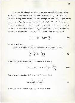
factor is 2.2 mv/deg C, the condition for zero thermal drift is
0.0071. = 0.0022gdz ^mz
(49)
Xdz~- = 0.315 volts
"mz
where gmz and I&z
are the transconductance and the drain current
respectively at the zero-drift bias point.
To proceed further, other expressions for I, and o mustd jmz
be developed. For a double-diffused FET, (see Fig. 3) the drain
current for any value of gate-to-cource voltage between zero and
pinch-off voltage V is.:P
VCS 2
Jd * V 1 " -F> (50)
P
where Id
is the drain current at VGS
= 0. Equation (50) is called
the square-law approximation (14)
.
A similar expression for g was derived in equation (30)
i.e.
32
g ='mz
3Id
3VGS
(51)
or
31g = _£ymz v
P(1 -
V
-f.)p
(52)
Dividing equation (50) by equation (52) gives
JL » _E /Ia 2
(1'mz
VGS,
P(53)
substituting equation (53) into equation (49) gives
V0.315 = -2- (1
VGSt,V '
P
or
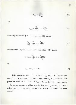
VGSZ = V
P" °- 63 (54)
This equation shows the value of V„GS
which will ijive zero
drift. It also shows that for a FET with V -P
0.6 3 volts , the
point of zero drift occurs at Vr_= , or X
d= I . More
Pimpor-
tant, these equations allow prediction of*dl
and g at zero
drift for devices with V aboveP
0.63 volts (3) Thus , at zero
drift,

33
Id-I
p(2^,
2
(55,
a = _JP- (°- 63) (56)ymz V K V '
( '
P P
Equation (55) reveals that devices with a large V must operate
at an I, very much below I to achieve zero drift. For example,
if V is 6.3 volts, I, must be one per cent of I .
P dz rp
For a given device type, unit-to-unit variations of 1 and
V are interrelated by the empirical equation (10)
,
Ip
= KVp
1 - 6 (57)'
where K is a function of the device geometry.
Substituting equation (57) into equation (55) gives
9mz = Kl<^>°-4
(58 '
P
and substituting equation (57) into equation (56) gives
9mz = K2<f>0,4
<")P
Equations (58) and (59) show that, when a field-effect
transistor is biased for zero drift, both I, and g are inversedz ^mz
functions of V. Therefore, low V devices are perferable forp p r
most applications (10) .
34
If a FET is biased at other than the zero-drift bias, what
effect will the temperature-induced change in I , have on V '
It has already been found that the change in depletion layer thick-
ness causes V__ to change at a rate of -2.2rav/deg C. Assuming
that the change in mobility causes I, to change 0.7 per cent/deg
C, then the quantity 0.007 (I,/g ) represents the corresponding
change, in volts/det C, of V _ (3). Thus, the net drift is
I.,
D = 0.0022 - 0.007(—
)
(60)<?m
in volts/det C.
Dividing equation (50) by equation (52) reveals that
I. V V-S = -^ (1 - -§i) • (61)
Substituting equation (61) into equation (60)
,
D = 0.0022 - 0.007 -£(1 - -^.) (62)
P
Rearranging equation (50) , it can be seen that
VGS
Xd
1/2(1 - -§§.) = (~) (63)
P P
Substituting equation (63) into equation (62)
,
35
V I 1/2D = 0.0022 - 0.007 -^-(jF5-) (64)
P
But, from equation (52)
Then
(I J
1/2 = E_(i l
1/2 (65)1V 0.63 U dz'^ 3;
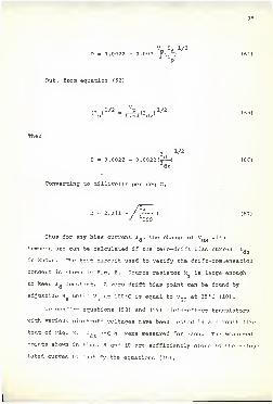
D = 0.0022 - 0.0022(Ti-) (66)
Converting to millivolts per deg C,
D = 2.2(1 - /=J— ) (67 )
/ DSS
Thus for any bias current I., the change of V„gwith
temperature can be calculated if the zero-drift bias current I,dz
is known. The test circuit used to verify the drift-compensation
concept is shown in Fig. 8. Source resistor R is large enough
to keep I&
constant. A zero-drift bias point can be found by
adjusting R until V at 100°C is equal to V„ at 25°C (10).s p Gb
To confirm equations (58) and (59) field-effect transistors
with various pinch-off voltages have been tested in a circuit like
that of Fig. 8. 1^ and gm were measured for each. The measured
points shown in Figs. 9 and 10 are sufficiently close to the calcu-
lated curves to justify the equations (10)
.

36
+ 30 v
Fig. 8. Test circuit for finding zero-drift bias point.
The simplest circuit for zero-drift is the source follower,
illustrated by the test circuit of Fig. 8. This circuit has no
voltage gain, but can be used as an impedance transformer. The
thermal drift of this circuit is comparable to that of a high-
quality differential amplifier (10) . Since voltage and current
drift can be reduced to very low levels, field-effect transistors
permit design of d-c amplifiers which exhibit little change in
operating point even with generator impedances greater than one
megohm (10)
.
Selecting the Best FET
As might be expected, values of I, and g are proportionalaz ^m c
to the size of the field-effect transistor. Also, as in pointed
out previously, field-effect transistors with low V have higherP
I-„ and g .

37
0)
10
oe
4
3 \
?
\V
1
V
\\0. 8 V
\0.6 h
0.5
\
100 200 300 400 600 100
I., microamperesa
Pig. 9. Drain current at zero drift for variousvalues of pinch-off voltage. The cross repre-sent measurements made in the circuit of Fig. 8.
The line represents values calculated from eg. (58)
01
01
c
4
3\
V
1x\
n.R \
Vn 6
0.5\
500 800 1000 2000 3000 5000
g , micromhos
10. Transconductance at zero drift forvarious values of pinch-off voltage. Theline represents calculated values from eq (59)
38
Field-effect transistors with higher I. are desirable for
anrolifiers in which a junction transistor is used in the second
stage. Field-effect transistors with low I, are more seriously
affected by the loading of a junction transistor, here, a second
field-effect transistor, with its very low current drift, is the
ideal choice for the second stage.
In selecting the best type of field-effect transistor for an
application, a compromise must be made between the very large in-
put impedance and the low input current drift of the small-geometry
field-effect transistor and the ease of circuit design afforded by
the higher drain current of large field-effect transistors.
Circuit Design
As any given FET type may have as much as 5:1 spread in I
and 4:1 spread in g , particular attention must be given to cir-
cuit design to ensure that any device within specifications will
perform satisfactorily (16) . Consider a common-source self-biased
amplifier design of Fig. 11. It is helpful to have a plot availa-
ble of the approximate minimum and maximum transfer characteristics
of the device. The d-c operating point for any device within the
range may be determined by constructing a source load line from
the origin with a slope of 1/R_ intersecting with the two curves.
It is desirable to ooerate with a small R for minimum distortion,s
but with a large R for constant drain current 1^. The range of
the ouiescent I, has now been determined; however, the peak sig-a
nal current i must be added. This is determined by superimposingDm a v
39
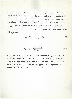
the gate signal voltage on the operating point. To maintain a
reasonably low distortion level, the signal swing as projected
on the minimum transfer curve must be small compared with the
curvature of that characteristic (16) . The peak signal current
ij has been determined; the maximum allowable R, may befl(max)
' *
determined. Remembering that the V__ should not drop below about
1.5 V , then
and
VDG " V
D - % ,\ < 68 >
(max)
V__ - 1.5VRL = -I
& (69)(max
>D(max)
Stage gain may be increased only be increasing R_ . To do this
it is necessary to increase V , reduce i, and/or V or select
a field-effect transistor with a smaller spread in I (17) . As
some field-effect transistors are typed with I spreads of 3:1
their use may be of some advantage (17)
.
40
' (max
' (min)
"out
1
Fig. 11(a). Self-biasedamplifier.
(max)
P(mirK '(max)
GS
Fig. 11(b). Transfer characteristics.
41
SMALL-SIGNAL LOW FREQUENCY-PROPERTIES
The channel current of a field-effect transistor actually
flows in a nonlinear distributed RC transmission line, but for
low frequency work it is sufficient to treat the device as if it
were a lumped nonlinear electrical network. An equivalent cir-
cuit showing the lumped parameters necessary for low frequency
calculations is given in Fig. 12. Capacitances CD(
, and Cg(
, and
conductances g_„ and g__ are a lumped-element representation of
the reverse-biased gate-to-channel diode. In a well designed
^SG
Fig, 12. Low frequency equivalent circuit for FET.
field-effect transistor, gnf, and g__ will be quite small and can
be considered open circuits. VAlues rD_ and r„
Bare the bulk re-
sistances of the semiconductor path from the channel edges to the
drain and source respectively; they will be in the order of 100
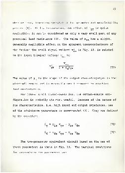
42
ohms or less, depending somewhat on the geometry and manufacturing
process (9). At low frequencies, the effect of rn„ is quite
negligible; it can be considered as only a very small part of any
practical load resistance (9) . The value of r„_ has a slight,
generally negligible effect on the apparent transconductance of
the device; the small signal voltage v' in Fig. 12, is related
to the input terminal voltage v by
VV' = 2£9s l + VSB (70)
The value of g is the slope of. the output characteristics in the
pinch-off region and is generally small compared to practical
load conductances.
For linear small signal-operation, the common-source con-
figuration is probably the most useful. Because of the nature of
its characteristics, i.e. high input and output impedances, use
of the admittance parameters is recommended (9) . They are defined
by the equations
i = y. v + y v. (71)g is gs J rs ds
i, = y, v + y v. (72)d J fs gs -'os ds
The two-generator equivalent circuit based on the use of
these parameters is shown in Fig. 13. The terminal conditions
for determining the parameters are

43
Fig. 13. Two-port y-network.
1
Output shorted: y. = -^2—gs
Input shorted:
'fsgs
CIS
"us
When these conditions are applied to the physical equivalent
circuit of Fig. 12, the y parameters can be written in terms of
the lumped physical elements. If all the diode conductances and
bulk resistances of Fig. 12 are neglected, the y parameters (9)
are :
3»< CDG+ C
SG>(73)
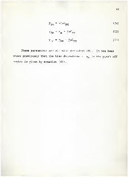
44
'rs = "^CDG < 74 >
'fs = <*m" ^C
DG (75 >
f S" *DS
+ ^CDG (76)
These parameters are all bias dependent (9). It has been
i previously that the bias di
region is given by equation (4 4)
shown previously that the bias dependence of g in the oinch-off

45
SMALL-SIGNAL EQUIVALENT CIRCUIT
It is now possible to develope a low frequency circuit for
the field-effect transistor by using equations (71) and (72) . Both
equations (71) and (72) have dimensions of current, and thus the
right hand side of each equation suggest the summing of currents
entering a junction. Figure 13 illustrates the simplest and the
most obvious two-current-generator equivalent circuit that can be
developed from equations (71) and (72)
.
A small equivalent low frequency circuit of Fig. 13 can be
used to describe the incremental .linear behavior of the field-
effect transistor. Because the input-gate current I is assumed
to be negligible (let I = 0) , both y. and y in equation (71)
are equal to zero. Hence,
= ° Vgs
+ ° Vds < 77 >
*« " Vgs + Vds (78 >
redefining,
'fs= g and y « o.
where g is the small-signal low frequency transconductance of
the device and g, is the small-signal output conductance of the
device.
Thus equation (78) is the only equation of any importance in
field-effect transistor small-signal equivalent circuit analysis.

46
The equivalent small-signal circuit for the field-effect transis-
tor is shown in Fig. 14.
The assumption that 1=0 greatly simplifies the equivalent
circuit of Pig. 13. This assumption also emphasizes that a field-
effect transistor is not necessarily a current amplifier but also
a voltage amplifier.
Fig. 14. Small-signal low frequencyequivalent circuit of the field-effect transistor.
From this equivalent circuit the voltage gain of the device
can be easily obtained if the device is operated in the pinch-off
region of its characteristics (20) . If a load JL is applied to the
output of Fig. 14, the expression for the gain is
Vgs
(79)
47
gs^d
+R
ds(80)
'ds1 + 1*\ (81)
therefore
Vlr + ^ (82)
As long as g.R. << 1 then A = g_Rr • Tne value of A varies
linearly with P_ and can be made quite large by making R. large
(20). When R_ becomes extremely large, so that g^Ry >> li
g|a I : — , (20) . This ration of the two parameters is known asV 1 g
d
amplification factor u of the field-effect transistor. The value
of v is quite small in the non-pinch-of f region of the characteris-
tics but it becomes appreciable in the pinch-off region of the
characteristics. This is the main reason that the device is
operated in the pinch-off region of the characteristics (20)
.
The input impedance for the small-signal application of the
common source field-effect transistor amplifier is particularly
easy to obtain, since the gate current is assumed to be zero in
theory, or

48
VGS
Z. - -S - - (83)in Ig
However for most devices the gate current is of the order of
nanoamperes. So for all practical purposes when calculating the
input impedance it is very large and may often be considered an
open circuit.

49
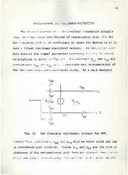
FIELD-EFFECT TRANSISTOR AMPLIFIERS
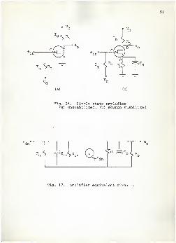
Basic FET Amplifier Configurations
The field-effect transistor, like the other three-terminal
active networks, can be operated with any of its three terminals
common in an amplifier circuit. The three basic amplifier con-
figurations are shown in Fig. 15 a-c, which are common-source,
common-gate, and common-drain amplifiers respectively. In each
of these connections it is possible to reverse the input and
output terminals pairs, giving altogether six possible combina-
tions, but the three connections shown are the only ones that
have any major applications.
The field-effect transistor symbol shown in Fig. 15, indi-
cates the interchange-ability of the drain and the source ter-
minals. Without some special marking, the drain is indistin-
guishable from the source. Hereafter, the drain will be desig-
nated by the symbol D as in Fig. 15. The symbol shown indicates
a P-channel FET; for an N-channel FET, the arrow on the gate
terminal is reversed.
output
input inout output input
output
(a) (b) (c)
Fig. 15. Basic amplifier configurations: (a) commonsource, (b) common gate, (c) common drain.
50
Voltage Amplifier Circuit
In the past, high input impedances in amplifiers could only
be obtained using vacuum tubes. Today, less complicated and
more reliable designs are possible with high-quality field-
effect transistors. A relatively high-input impedance solid-
state amplifier will be discussed in this section and some in-
sight into biasing techniques is provided to show that field-
effect transistors are compatible with and complementary to
conventional transistors. The amplifier analyzed here is built
around a p-channel field-effect transistor and an npn bipolar
transistor in the following stage.
In the design of a high-input-impedance amplifier, biasing
at the input must be carefully considered as has been pointed
out previously. Although the input impedance of the FET is very
high as compared to the conventional bipolar transistor, it is
necessary, if reasonably stable operation is to be achieved, to
provide a d-c current path from the gate to source. The d-c
gate current of the type 2N2606 field-effect transistor has been
-9shown to be less than 10 amps at room temperature; at 100° C,
_ohowever, it may increase to about 5 x 10 amps (8) . This cur-
rent must be considered in setting up the bias for the FET.
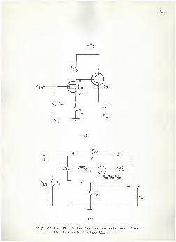
In the voltage amplifier circuit in Fig. 16a, the gate
bias is
VGS = V
G - VG (84)
51
d <RT
i«C
A.
<U
-o eD O
cr
G R
(a) (b)
Pig. 16. Single-state amplifier(a) Unstabilized, (b) source stabilized
RgS T C-> r^ Qe f S"o <s. R
Fig. 17. Amplifier equivalent circuit.
52
If, for example, an input impedance of 10 ohms is desired, the
7value of RG
must be at least 10 ohms since it shunts the input
(8), In this case, the gate bias V „ may change as much as
0.5 v, due to IqKg
- When the temperature is raised from 25" C
to 100° C. For some applications this may be tolerable; how-
ever, this change will result in considerable variation in drain
current and transconductance (8) .
Another undesirable aspect of the circuit of Fig. 16a is
the dependence of drain current I upon temperature. If V is
held constant, Id
will decrease as the device temperature in-
creased. Since transconductance g is a function of drain cur-
rent, it will also decrease. If the amplifier is to operate over
a reasonable ambient temperature range and with a reasonable
production spread of device parameters, some form of bias stabil-
ization must be used (8)
.
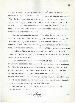
Bias stabilization for the circuit of Fig. 16b is achieved
by negative feedback, due to the I-R drop across source resistor
Rg. This is the same type of current feedback provided by the
emitter resistor in a conventional transistor circuit and the
cathode resistor in a vacuum tube circuit. A change in source
current will result in a change in source voltage, and thus 4VGS
is such as to oppose the initial source-current change. Capaci-
tor Cg
serves to bypass R for a-c signals.
The voltage amplification of the circuits in Fig. 16 is
given by equation (82) .

53
G N?d Dlo
D*L
-°e as
r i
l4
^F
'gs
£© >
g e~m gs S.
(a) (b)
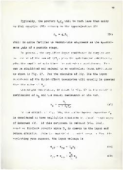
Fig. 18. (a) Amplifier with unbypassed source resistor,(b) Equivalent circuit.
9~VD
-<3*T
\
*S
'gsa em gs
Lo<S
(a) (b)
Fig. 19. (a) Source follower circuit,(b) Equivalent circuit.
rV„
54
^
$
£(a)
(b)
Fig. 20 (a) Unioolar-bipolar cascade amplifier(b) Equivalent circuit.
55
Typically, the product R^ g , will be much less than unity
so that equation (85) reduces to the approximation (8)
Av = %R
L(86)
which is quite familiar to vacuum-tube engineers as the approxi-
mate gain of a pentode stage.
In general, the amplifier input admittance is complex and
is made up of the sum of 1/R_, plus the gate-source admittance,
plus the amplifier gain times the gate-drain admittance. This
can be simplified and reduced to an equivalent input admittance
as shown in Fig. 17. For the circuits of Fig. 16a the input
resistance of the field-effect transistor will usually be greater
than the value of R_.
The output resistance, as shown in Fig. 17 is the parallel
combination of R, and the output resistance of the FET.
In the circuit of Fig. 16b, the source bypass capacitor C
is considered to have negligible reactance at signal frequencies
of interest (8) . If this component is omitted (Fig. 18a)
,
negative feedback results since R is common to the input and
output circuits. From the equivalent circuit shown in Fig. 18b
neglecting gate current, the input voltage is
eiN - e
gs+ Vs (88)
eiN = e
gs+57
eo
(89)
56
The feedback factor B is the ratio of R to R-, thus the voltage
amplification is given by
\ %RT < 90 >
1 +V u
RL
substituting equation (86) into equation (90) yields
Av
=1 + g R < 91 >
^m S
If 9mRs is made large with respect to unity, equation (91)
becomes
•
RL
Av = ig < 92 >
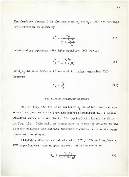
The Source Follower Circuit
If, in Fig. 19a the load resistor R^ is eliminated and the
output voltage is taken from the feedback resistor R , a source-
follower circuit is obtained. The equivalent circuit is shown
in Fig. 19b. This will be recognized as being equivalent to the
emitter follower and cathode follower circuits and has the same
types of advantages.
Following the equivalent circuit of Fig. 19a and neglecting
FET capacitances, the output current can be written as
e g• _ gs Jm ,-«,Xo " (1 + gd
Rs
)<«>
57
the output voltage
and the input voltage
e g Re - i R = ,f
m sp . (94)
o os (l + glRJ
ein = e
gs+ e
o - egs
l +(i
g
+ gdRs
< 95)
Dividing equation (94) by equation (95) leads to the voltage
amplification:
e g P.
Av " i— - (i + Rjg+g„ )
(96)in s m 3a
The output impedance of this circuit is greatly reduced from that
of the circuit in Fig. 16b, as indicated by
% = i +\(gm+gd >
(9?)s ^m a
Another important characteristic of the source-follower is a
reduced input admittance. The gate-source component of the
effective input capacitance is reduced as shown below:
C = C (1 - A ) (98)gs gs v
where C = gate-to-source capacitance.

58
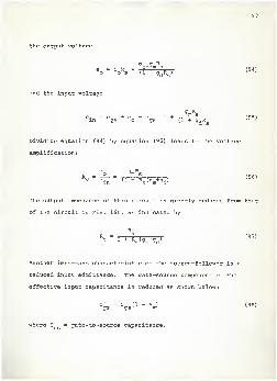
FET Cascade With Bipolar Transistor
Where it is desired to couple a very high-impedance source
to a low-impedance load, a unipolar-bipolar cascade transistor
stage is a good circuit. Such a circuit is shown in Fig. 20a. The
similarity between this circuit and the source follower of Fig.
18a should be noted. To a first approximation, the improvement
in performance (8) can be determined by multiplying the g of
FET Q. by the h- of the npn bipolar transistor Q, . If the out-
put admittance of the combination of Q, and Q, , gj, is assumed to
be small compared to g_hi and 1/R„ , the voltage amplification of
Fig. 20b can be written
e g h!. RA = -2_ = m fe 5
(99)Av e. 1 + Q h' R
(b,S '
In -m fe s
In equation (99) and in the equivalent circuit of Fig. 20b,
fe fe R„+h.D ie
(100)
where h. = current gain of Q_
and h. = input impedance of Q_
.
Equation (99) is similar to Equation (96) except that g. has been
neglected and the factor hi has been introduced to account for
the additional current gain of the bipolar transistor. The cas-
cade circuit is useful for video amplifiers or RF amplifiers up
to about 100 MHz. Noise figures of less than 2DB are realized at
100-200 KHz. (3)
.
59
THE POWER FIELD-EFFECT TRANSISTOR
Junction power field-effect transistors have some provoc-
ative characteristics for applications through VHF. Currently
available units exhibit an output current (I,) of one amp with
an input current (I ) of 1 nA, making them easier to drive than
(17) their bipolar counterparts. (power supply regulators?).
These new FETs can be turned on (5 ohms) and off (5000 megohms)
in less than 20 nanoseconds (core drivers?) , and they have zero
offset voltage. (store and hold circuits?) (D-to-A ladder
switches?) (17)
.
Conventional bipolar transistors suffer from a conflict
of interests when it comes to power and frequency, because high
current dictates large junction area and high feedback capaci-
tance, while high voltage means large base width and reduced
gain. In the FET, junctions can be kept small because current
flows between the junctions rather than through them. Also,
maximum voltage is determined by gate diode breakdown, and has
no first order effect on gain.
The power FET looks pretty good as an RF amplifier. For
one of the newest types, the calculated F is 1.5 GH (17).
As a result of the low intermodulation distortion inherent in
FETs in general, and the low noise resistance of these new high
current devices in particular, an evaluation unit has demon-
strated over 140 DD of dynamic range operating as an RF front
end (17).
60
While currently available power FETs are not about to
obsolete their bipolar predecessors, they are certainly worthy
of investigation.
61
CONCLUSIONS
The field-effect transistor, or FET, as discussed in this
report is an excellent choice for amplifier circuit applications
requiring; high input impedance, low d-c input current, low
harmonic distortion, low noise and zero d-c drift.
The characteristics which suit the field-effect transistor
to these applications requirements are: reverse-biased diode
9 13input characteristic providing 10 to 10 ohms d-c input resis-
tance; square law transfer characteristic allowing only second
order harmonic distortion; noise levels as low as e. = 20 nv/Hi"In
at 10 Hz and NF < db, and d-c drift as low as 1 uv/°C when prop-
erly biased.
Those amplifier applications where field-effect transistors
are now, or are destined to be widely used are (17) electrometer
and charge sensitive amplifiers, low drift d-c amplifiers, RF
and mixer circuits requiring low cross-modulation levels, low-
noise audio, video, and RF applications, low distortion audio
circuits, and high-impedance audio or video applications. Each
amplifier application may be considered individually relating
to pertinent field-effect transistor characteristics.
The field-effect transistor has been principally known for
its high input impedance characteristic. The gate input impedance
is a function of the physical size and quality of the gate
junction. The d-c leakage current I of the junction FET may
be below 1 pA at 30 volts (17) ; this is equivalent to 1013
ohms
input impedance.
62
In biasing a field-effect transistor for extremely low gate
current applications, the source follower configuration is best,
as the gate-source voltage may be minimized over the range of
input signal swing. Drain-gate voltage V,,,, should also be theDG
lowest practical value in order to reduce gate-drain leakage to
a minimum. The operating gate current I is then less than Ig P
by an order of magnitude depending upon the gate-source V„_ andGS
drain-gate V voltages.
A single field-effect transistor connected in a common-
source or common-drain configuration may be biased to operate
with a true zero temperature coefficient. This characteristic
is unique to field-effect transistors and is due to two counter-
acting temperature effects. One effect is, by now, well known
in transistors as a temperature sensitive base-emitter voltage
VBE>
The gate junction of a field-effect transistor exhibits
the same approximate -2.2 mV/°C temperature dependence which
causes the drain current to exhibit a positive temperature co-
efficient. Another effect is a negative temperature coefficient
drain current due to decreasing carrier mobility. At one cer-
tain value of drain current, these two effects exactly cancel,
and drain current and gate-source voltage remain constant with
temperature.
A field-effect transistor is free of the noise generated
in a conventional bipolar transistor; the source of noise in the
latter is due to carrier recombination in the base. In the
field-effect transistor, the current flow is simply majority

63
carrier flow just as in a metal conductor. Radiation reduces
minority carrier lifetime thus degrading conventional transis-
tors (13) . The transconductance of field-effect transistor is
independent of this lifetime and is therefore insensitive to
this type of radiation damage (12)
.
Finally, due to such applications as have been described
of the field-effect transistor, it is reasonable to say that had
industry first concentrated on perfecting the field-effect
transistor rather than the bipolar injection type now so preva-
lent, most circuits would be using field-effect transistors.
Injection types would play a special role only-a complete rever-
sal of the actual situation today.

64
REFERENCES
(1) Bockemuehl , R. R.Analysis of field-effect transistors with arbitrary chargedistributions, IEE Trans, on Electron Devices, Vol. ED-10,pp. 31-34, January 1963.
(2) Bockemuehl, R. R.Field-effect modulation of photoconductance , J. Appl . Phys .
,
Vol. 31, pp. 2256-2259, December 1960.
(3) Buckholz, W.Biasing a FET for low drift, Electronics, p. 92, May 30,1966.
(4) Bruncke, W. c.Noise measurement in field-effect transistors, Proc. IEEE,Correspondence, Vol. 51, p. 378, February 1963.
(5) Cobbold, R. S. C. and Trofimenkof f , F. N.Theory and application of the field-effect transistor, Proc.IEEE, Vol. Ill, No. 12, pp. 1981-1991.
(6) Cowles, Laurence G.Measurement of FET pinch-off voltage, Proc. IEEE, p. 200,February 196 4.
(7) Dacey, G. C. and Ross, I. M.The field-effect transistor, Bell System Tech. J., Vol. 34,pp. 1149-1189, November 1955.
(8) Evans, A. D.Analyzing high-input-impedance FET amplifiers, ElectronicEquipment Eng., Vol. 11, p. 72, March 196 3.
(9) Evans, A. D.Characteristics of unipolar field-effect transistors,Electronic Industries, Vol. 22, p. 99, March 1963.
(10) Evans, L. L.Biasing FETs for zero D-C drift, Electro-Technology, p. 94,August 1964.
(11) Gibbons, J. F.Semiconductor Devices, McGraw-Hill Book Company, 1966.Chapter 6
.
65
(12) Phillips, Alvin B.Transistor engineering, McGraw Hill Book Company, 1962,Chapter 4
.
(13) Radeka, V.Field-effect transistor-its characteristics and applications,IEEE Trans, on Nuclear Science, pp. 358-364, June, 1964.
(14) Richer and Middlebrook.Power law nature of field-effect transistor, Proc. IEEE,p. 1145, August 1963.
(15) Roosild, S. A., Dolan, R. P., and O'Neil, D.A unipolar structure applying lateral diffusion, Proc.Inst. Electrical Electronics Engrs . , p. 1824, 1963, 51.
(16) Sevin, S.
A simple expression for the transfer characteristics ofa FET, Electronic Equipment Engineering (EEE) , p. 59,August 1963.
(17) Sherwin, J. S.Field-effect amplifiers. Electronic Communicator, p. 3,January/February 196 7.
(18) Shockley, W.A unipolar field-effect transistor, Proc. IRE., Vol. 40,
pp. 1365-1376, November 1952.
(19) Uzunoglu, VasilSemiconductor network analysis and design, McGraw-Hill BookCompany , p. 68, 196 4.
(20) Van der Ziel, AlbertElectronics, Allyn and Bacon, Inc., p. 103, 1966.
(21) Wang, ShyhSolid State Electronics, KcOraw Hill Book Company, 1966,Chapter 3.
66
ACKNOWLEDGMENT
The writer is indebted to Dr. W. W. Koepsel, Chairman of
the Department of Electrical Engineering, for providing a faculty
position of instructor from September 1, 1965 - June 1, 1967.
The writer also wishes to express his deep appreciation to Profes-
sor Joseph E. Ward, Jr. (advisor) for his valuable suggestions
and positive influence during the preparation of this report.
The writer wishes to thank the other members of his committee,
Dr. F. W. Harris and Professor L. A. Wirtz for reading this re-
port with interest.
67
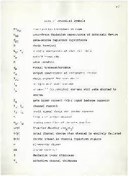
List of Principal Symbols
BVdgs
reverse-bias breakdown voltage
CDS
gate-drain depletion capacitance of intrinsic device
CSG
gate-source depletion capacitance
D drain terminal
E , Ex' y
x and y components of electric field
Tcutoff frequency
G gate terminal
?mmutual transconductance
gdoutput conductance of undepleted channel
Xdz
drain current for zero drift
ig
small-signal gate current
ip
pinch-off (saturation) current with gate shorted to
source
zg
gate input current (also input leakage current)
V Jd
channel current
id' * small signal drain and source current
L length of active channel
A Ddoping densities of abrupt- junction
p(y) impurity density q(N -N )
Q(y) total channel charge when channel is entirely depleted
0(t) charge stored in channel depletion regions
q electronic charge
ss source terminal
t depletion layer thickness
Tc
effective channel thickness

68
T. half-thickness of channelnC
T depletion layer thickness at the source
T. depletion layer thickness at the drain
V drain-bias voltage (relative to source)
V _, v, drain-to-source voltage
V gate-bias voltage (relative to source)
V , v gate-to-source voltage
w width of channel
e dielectric constant
u mobility of majority carriers in the channel
Pi free charge density of channel
P space charge density (fixed)
THEORY AND APPLICATIONS OF FIELD-EFFECT TRANSISTORS
by
JOE WILLARD TOLIVER
B. S. r Prairie View ASM College, 1962
AN ABSTRACT OF A MASTER'S REPORT
submitted in partial fulfillment of the
requirements for the degree
MASTER OF SCIENCE
Department of Electrical Engineering
KANSAS STATE UNIVERSITYManhattan, Kansas
1967

The junction field-effect transistor (FET) has a conducting
channel that connects its source and drain terminals. The con-
ductivity of this channel can be modulated by the electric field
of the reverse biased gate-to-channel junction diode; thus the
name junction field-effect transistor. Three characteristics of
the junction field-effect transistor make it very attractive as
an active semiconductor device. (1) Low gate current and thus
high input impedance, (2) Low noise, and (3) Excellent stability.
The d-c theory and small signal properties of the junction
field-effect transistor are presented analytically. The analysis
is based upon an active transmission line analogy to the con-
ductive channel of the FET. Within limitation of the gradual
channel approximation, general exDressions for the channel current,
pinch-off voltage, mutual transconductance , output conductance,
and junction capacitance are derived as functions of the depletion
layer thickness at the device boundaries. Equivalent small sig-
nal circuits are obtained which describe the junction field-effect
transistor characteristics in the region below pinch-off as well
as in the pinch-off region.
The effects of temperature on the device are considered in
detail. It is shown that provided certain conditions are ful-
filled, the device can be biased so as to operate with almost
zero drift over a wide temperature range.
Related Documents