The Pennsylvania State University The Graduate School College of Engineering THE SHAPE SYNTHESIS OF DIELECTRIC RESONATOR ANTENNAS FOR WIRELESS COMMUNICATION SYSTEMS A Dissertation in Electrical Engineering by Hamad Alroughani © 2018 Hamad Alroughani Submitted in Partial Fulfillment of the Requirements for the Degree of Doctor of Philosophy December 2018

Welcome message from author
This document is posted to help you gain knowledge. Please leave a comment to let me know what you think about it! Share it to your friends and learn new things together.
Transcript

The Pennsylvania State University
The Graduate School
College of Engineering
THE SHAPE SYNTHESIS OF DIELECTRIC RESONATOR
ANTENNAS FOR WIRELESS COMMUNICATION SYSTEMS
A Dissertation in
Electrical Engineering
by
Hamad Alroughani
© 2018 Hamad Alroughani
Submitted in Partial Fulfillment
of the Requirements
for the Degree of
Doctor of Philosophy
December 2018
ii
The dissertation of Hamad Alroughani was reviewed and approved* by the following:
James Breakall
Professor of Electrical Engineering
Dissertation Advisor, Chair of Committee
Ram Narayanan
Professor of Electrical Engineering
Julio Urbina
Associate Professor of Electrical Engineering
Antonios Armaou
Associate Professor of Chemical Engineering
Derek McNamara
Professor of Electrical Engineering at University of Ottawa
Special Member
Kultegin Aydin
Professor of Electrical Engineering
Head of the Department of Electrical Engineering
*Signatures are on file in the Graduate School

iii
ABSTRACT
Antennas are needed in wireless communications of any kind and are key to the quality of any
wireless link, irrespective of its use. The abilities needed of a particular antenna depend on its
application, and so the cost of antennas in current use varies from a few cents for those in mobile
devices, to many millions of dollars for the main mission antennas on satellites or sophisticated
radar antennas in military use. They are indeed the eyes and ears of modern wireless
communications systems. Dielectric resonator antennas are one of the popular antenna types and
hold the promise of requiring less room for proper operation, in essence due to the loading effect
of the material. The principal original contributions to antenna shape synthesis is presented in this
dissertation; an approach is devised for the three-dimensional shape synthesis of dielectric
resonator antennas which are subject to geometry restrictions. It is entirely new, representing the
first time any three-dimensional shape optimization of dielectric resonator antennas has been
described. It is particularly novel because, not only does it shape the dielectric material, but it
permits the shape optimization process to proceed without the restriction of a pre-determined feed-
point location. The approach is made possible through properly connecting antenna performance
parameters to the use of characteristic mode concept which allows the computation of modal
weighting coefficients using the surrogate source idea that is established. These coefficients are
then used in the definition of the objective functions. The shape synthesis technique was
successfully applied to three dielectric resonator antenna examples, each with different design
requirements and constraints. Its success in these cases demonstrates the effectiveness of the new
shaping technique. Computed performance is supported by experimental results. The
implementation of the shaping tool itself, apart from being needed to validate the shaping process,
is an addition in its own right. It has purposefully been fully implemented using commercially
available software, for the computational electromagnetics, the optimization algorithm, and the
controller that manages the shaping process and allows communication between the various steps.
The advantage of being able to use such commercial codes is that the approach at once becomes
more accessible to others. The determination of the characteristic modes of dielectric objects has
been fraught with difficulties, and there have been uncertainties in the literature as to precisely
what was being computed. A number of aspects of characteristic mode theory therefore had to be
investigated and repaired before the shape synthesis work could proceed. Although they might not
be linked directly to the shape synthesis process, other significant contributions are related to the
characteristic mode analysis by developing a more robust method for tracking the characteristic
modes of dielectric objects, presenting a more general (broadened) formulation of the sub-structure
characteristic mode concept and providing formal mathematical proofs of the orthogonality
properties of sub-structure modes.
Keywords:
Shape optimizations, dielectric resonator antennas, material properties characterization,
characteristic modes, antenna shape synthesis, method of moments, surface integral equations,
volume integral equations, additive manufacturing, MIMO.

iv
TABLE OF CONTENTS
LIST OF FIGURES ...................................................................................................................... vii
LIST OF TABLES ......................................................................................................................... xi
LIST OF ABBREVIATIONS ....................................................................................................... xii
ACKNOWLEDGEMENTS ......................................................................................................... xiii
CHAPTER 1: INTRODUCTION ............................................................................................. 1
ANTENNAS: THE EYES & EARS OF MODERN WIRELESS COMMUNICATIONS
.......................................................................................................................................... 1
ANTENNA TYPES ......................................................................................................... 1
OVERVIEW OF THE THESIS ....................................................................................... 2
CHAPTER 2: ANTENNA SYSTEM REQUIREMENTS, ANALYSIS & SYNTHESIS ....... 4
INTRODUCTION ............................................................................................................ 4
ANTENNA REQUIREMENTS DRIVEN BY MODERN COMMUNICATIONS
SYSTEM DESIGN ..................................................................................................................... 4
DIELECTRIC RESONATOR ANTENNAS: STATE OF THE ART............................. 9
DRA Conventional Shapes ....................................................................................... 9
DRA Modes ............................................................................................................ 11
DRA Feeding Mechanisms ..................................................................................... 11
DRA Materials ........................................................................................................ 14
DRA Bandwidth...................................................................................................... 14
DRA Unconventional Shapes ................................................................................. 15
DIELECTRIC RESONATOR ANTENNAS: ANALYSIS METHODS ....................... 18
Introductory Remarks ............................................................................................. 18
Statement of the Fundamental Physical Problem ................................................... 18
Approximate Analytical Solutions .......................................................................... 19
Computational Electromagnetics Modelling: Finite Element Method ................... 20
Computational Electromagnetics Modelling: Method of Moments ....................... 20
ELECTROMAGNETIC CHARACTERISTIC MODE THEORY................................ 24
Fundamental Characteristic Mode Concepts .......................................................... 24
Characteristic Modes of Conducting Objects ......................................................... 25
Characteristic Modes of Dielectric Objects ............................................................ 28
Sub-Structure Characteristic Modes ....................................................................... 29
Characteristic Modes of Dielectric Resonator Antennas ........................................ 31
WIRELESS COMMUNICATION SYSTEM REQUIREMENTS ................................ 31
ADDITIVE MANUFACTURING ................................................................................. 33
CHARACTERIZATION OF DIELECTRIC MATERIAL Electrical PROPERTIES .. 34
CONCLUSIONS ............................................................................................................ 36
CHAPTER 3: A CHARACTERISTIC MODE INVESTIGATION OF DIELECTRIC
RESONATOR ANTENNAS ........................................................................................................ 37
INTRODUCTION .......................................................................................................... 37
EXTENSIONS OF SOME BASIC CONCEPTS IN CHARACTERISTIC MODE
THEORY .................................................................................................................................. 37
Initial Remarks ........................................................................................................ 37

v
Non-Physical Modes – Comments on Earlier Work............................................... 37
Mode Tracking ........................................................................................................ 38
Sub-structure Modes – Broadened Concept ........................................................... 43
Sub-Structure Modes – Equivalence to Modes Determined from Integral Equations
with Modified Green’s Functions ......................................................................................... 47
Sub-Structure Modes – Extension to Composite Objects ....................................... 50
Sub-Structure Modes – Orthogonality Properties ................................................... 52
The Ubiquitous Conducting Groundplane .............................................................. 53
Controversies Regarding the CMs of Dielectric Objects ........................................ 55
CHARACTERISTIC MODES VERSUS NATURAL MODES ................................... 55
THE CONVENTIONAL RECTANGULAR DRA: DEFORMATION & SCALING .. 56
Map of the Systematic Examination of the CMs of Conventional DRAs .............. 56
Computational Electromagnetics Code Verification .............................................. 57
Square & Rectangular DRAs .................................................................................. 57
Dimensional Scaling of DRAs ................................................................................ 61
Material Scaling of the Square DRA ...................................................................... 61
Circular DRA .......................................................................................................... 62
Square DRA with Notch ......................................................................................... 63
3.5 CONCLUDING REMARKS ......................................................................................... 67
CHAPTER 4: Dielectric Resonator Antenna Shape Synthesis Tools .................................... 68
PRELIMINARY REMARKS ........................................................................................ 68
THE SHAPE SYNTHESIS TECHNIQUES .................................................................. 68
Shaping Technique using VIE-based MoM Approach ........................................... 68
Shaping Technique using BOR-based MoM Approach ......................................... 69
Shaping Technique using SIE-based MoM Approach............................................ 70
GEOMETRY & MATERIAL CONTROL .................................................................... 71
COMMENTS ON OBJECTIVE FUNCTION CONSTRUCTION ............................... 73
ILLUSTRATIVE CASE STUDY .................................................................................. 75
Probe Fed Square DRA ........................................................................................... 75
Probe Fed Unconventional Shaped DRA ............................................................... 80
CONCLUSIONS ............................................................................................................ 85
CHAPTER 5: Shape Optimized Dielectric Resonator Antennas ........................................... 86
INTRODUCTORY REMARKS .................................................................................... 86
SHAPE SYNTHESIS EXAMPLE #1: Optimized Bandwidth DRA ............................. 86
Preamble ................................................................................................................. 86
The Objective Function and Shaping Process ........................................................ 87
Parameter Settings for the Shaping Process ............................................................ 89
Outcome of the Shape Synthesis Process ............................................................... 90
Simulation and Measurement of the Completed DRA Antenna ............................. 93
SHAPE SYNTHESIS EXAMPLE #2: 2-port MIMO DRA ........................................ 101
Preamble ............................................................................................................... 101
5.3.2 The Objective Function and Shaping Process ........................................................... 101
Parameter Settings for the Shaping Process .......................................................... 103
Outcome of the Shaping Synthesis Process .......................................................... 104

vi
Simulation and Measurement of the Completed DRA Antenna ........................... 108
SHAPE SYNTHESIS EXAMPLE #3: Broadside Pattern and restricted size dra ....... 114
Preamble ............................................................................................................... 114
The Objective Function and Shaping Process ...................................................... 115
Parameter Settings for the Shaping Process .......................................................... 117
Outcome of the Shape Synthesis Process ............................................................. 118
Simulation and Measurement of the Completed DRA Antenna ........................... 121
CONCLUSIONS .......................................................................................................... 124
CHAPTER 6: General Conclusions ...................................................................................... 125
REFERENCES ........................................................................................................................... 127
APPENDIX A: Options for Genetic Algorithm ......................................................................... 132
APPENDIX B: The Fields of Infinitesimal Electric Dipole ....................................................... 135
APPENDIX C: Proofs of the Orthogonality Properties of Sub-Structure Characteristic Modes 137
APPENDIX D: The Guidelines in Designing the Starting Geometry of the sSlot Aperture Antenna
as a Feed ...................................................................................................................................... 141

vii
LIST OF FIGURES
Figure 2.1: (a) Radiation lobes and beamwidths of antenna patterns (b) Linear plot of power pattern
and associated lobes and beamwidths [BALA05]. ............................................................................ 8 Figure 2.2: Geometry of (a) hemispherical (b) cylindrical (c) rectangular DRA [PETO07]. .............11 Figure 2.3: A DRA is fed with a microstrip line in (a) and with a coplanar waveguide in (b) [HUIT12].
........................................................................................................................................................12 Figure 2.4: A DRA is fed with aperture coupling with a slot in the ground plane [HUIT12]. ............13 Figure 2.5: A coaxial probe is fed through a DRA (b) the coupled field inside the DRA (c) the coupled
field inside the DRA (top view) [HUIT12]. .....................................................................................13 Figure 2.6: The geometry of the pixilated DRA [TRIN16] ...............................................................16 Figure 2.7: The geometry of split cylinder resonator loaded with a smaller resonator for dual-band
operation [KISH01] .........................................................................................................................17 Figure 2.8: The geometry of H-shaped DRA, top and side view [LIAN08]. .....................................17 Figure 2.9: a scattering problem from a penetrable object. ...............................................................22 Figure 2.10: Two objects considered for the sub-structure CM analysis. ..........................................29 Figure 2.11: Instrument used in for material characterization using exact resonance method
[HAKK60]. .....................................................................................................................................35 Figure 3.1: the colored solid lines represents those modes tracked using the proposed method whereas
the circles represents the modes tracked using the technique in [RAIN12]. ......................................40 Figure 3.2: The eigenvalue of the dominant physical CM of the notched DRA shown as a function of
mesh size.........................................................................................................................................41 Figure 3.3: The of Pnn of the dominant physical mode, associated with Figure 3-2, at every frequency
iteration as a function of mesh size. .................................................................................................42 Figure 3.4: The of correlation values between the dominant mode, associated with Figure 3-2, at every
frequency iteration as a function of mesh size. .................................................................................42 Figure 3.5: Perfectly conducting (PEC) structure consisting of two parts. ........................................44 Figure 3.6: Plot of (a). 1 and (b). 2 versus frequency for a strip dipole above an infinite groundplane
using the appropriate modified Green’s function (▬ ▬ ▬), of the sub-structure modes for a large
rectangular finite groundplane (▬▬▬), and the sub-structure modes above a small groundplane
(▬▬▬)..........................................................................................................................................49 Figure 3.7 The eigenvalues of the two lowest sub-structure CMs of the strip dipole in the presence of
the dielectric block are (▬▬) λ1 and (▬▬) λ2. The eigenvalues of the two lowest conventional CMs
of the isolated strip dipole in free space are (▬ ▬ ▬) λ1 and (▬ ▬ ▬) λ2. There is no groundplane
present.............................................................................................................................................51 Figure 3.8: Calculating conventional CMs in (a) of an isolated DR compared to calculating the
modified CMs in (b) and (c) in which the presence of an infinite PEC ground plane is accounted for
by a modified Green’s function. The difference between (b) and (c) is the particular way in which the
DRA has been sliced in half. ...........................................................................................................54 Figure 3.9: CM eigenvalues corresponding to the geometries shown in Figure 3-8. The solid lines are
for geometry (a), the circled-lines for (b), and the crossed-lines for (c). Color variation signifies
different modes. ..............................................................................................................................54 Figure 3.10 Rectangular DRA (the square DRA being a special case). the dimensions are
8.77w d mm= = , 3.51h mm= , and dielectric constant is 37.84r = . .........................................57
Figure 3.11: Eigenvalues of the first four CMs of a square DR. .......................................................58

viii
Figure 3.12: Eigenvalues of the first four CMs of a “non-square” DRA compared to those of the square
DRA also shown in Figure 3-11.The non-square DRA.....................................................................58 Figure 3.13: a). Electric field magnitude, (b). Magnetic field magnitude, and (c). Far-zone field, plots
of the lowest order CM of the square DRA at its resonance frequency of 5.65 .................................59 Figure 3.14: (a). Electric field magnitude, (b). Magnetic field magnitude, and (c). Far-zone field, plots
of the 2nd order CM of the square DRA at its resonance frequency of 7.56 GHz. ............................60 Figure 3.15: Eigenvalues of the first four CMs of the original square DRA also shown in Figure 3-11
(solid lines) compared to the double scaled square DRA (dashed lines). All the eigenvalues are
represented with the same colour in this plot, the degenerate mode’s curves are laying on top of each
other’s. ............................................................................................................................................61 Figure 3.16: Eigenvalues of the first four CMs of the original square DRA also shown in Figure 3-11
(solid lines) compared to the same square DRA new
r increased to 50 (dashed lines). All the eigenvalues
are represented with the same colour in this plot, the degenerate mode’s curves are laying on top of
each other’s. ....................................................................................................................................62 Figure 3.17: Eigenvalues of the first four CMs of the boundary notched square DR shown the top left.
........................................................................................................................................................65 Figure 3.18: a). Electric field magnitude, (a). and Magnetic field magnitude, and (b), plots of the lowest
order CM of the boundary notched square DRA at its resonance frequency of 6.128 GHz ...............65 Figure 3.19: Eigenvalues of the first four CMs of the centered notched square DR. .........................66 Figure 3.20: a). Electric field magnitude, (a). and Magnetic field magnitude, and (b), plots of the lowest
order CM of the boundary centered notched square DRA at its resonance frequency of 6.58 GHz ...66 Figure 4.1: shaped DRA using VIE-based approach by removing tetrahedrons. ...............................69 Figure 4.2: the BOR approach applied to rotationally symmetric geometries [KUCH00a]. ...............70 Figure 4.3: A demonstration of voxelization in (a), symmetry in (b) and (c), and dispersed shape in (d).
The chromosome associated with each shape is indicated below each. .............................................73 Figure 4.4: Computational electromagnetics model of the antenna in all its detail. ...........................74 Figure 4.5: Computational electromagnetics model of the DRA antenna used during the shape synthesis
process (and hence for CM analysis). ..............................................................................................75 Figure 4.6: The configuration (side and top views) of the square DRA in [ZOU16]. The design
parameters are: a = b = 38 mm, c = 10 mm, r = 9.8, l = 10 mm and gl =100 mm. .........................76
Figure 4.7: The MWC of the square DRA due to the infinitesimal electric dipole source placed at the
center. .............................................................................................................................................77 Figure 4.8: The modal far fields for the corresponding to modes shown in Figure 4-7. .....................77 Figure 4.9: The modal electric fields corresponding to modes shown in Figure 4.7. .........................78 Figure 4.10: The modal magnetic fields corresponding to modes shown in Figure 4-7. ....................78 Figure 4.11: |S11| in dB for the square DRA fed with a center probe modeled in HFSS. ....................79 Figure 4.12: The geometry of the studied unconventional shaped DRA. ..........................................80 Figure 4.13: The MWCs due to an infinitesimal electric dipole placed at three different positions. The
curve colors (blue, red, and black) indicate modes considered (CM #1, CM #2, and CM #3). The curve
types (solid, dashed, dotted dashed) indicate the source position (1,2, and 3). ..................................81 Figure 4.14: The modal far fields in 3-D for the corresponding modes shown in Figure 4-13. ..........81 Figure 4.15: The modal electric fields in the DRA for the corresponding modes shown in Figure 4-13.
........................................................................................................................................................82 Figure 4.16: The modal magnetic fields in the DRA for the corresponding modes shown in Figure 4-13.
........................................................................................................................................................82

ix
Figure 4.17: |S11| in dB for the unconventional shaped DRA fed with a probe at the three different
positions. .........................................................................................................................................84 Figure 4.18: The gain in dB for x-z and y-z plane cuts in (a) and (b), respectively, for a coaxial probe
placed at position 1 (blue) , position 2 (red), and position 3 (black). .................................................84 Figure 5.1: Eigenvalue versus frequency plot for the unshaped rectangular object............................87 Figure 5.2: The starting shape for Example#1 shape optimization is divided into blocks and placed on
an infinite groundplane. The light-coloured block is simply meant to clearly identify an individual
block, but is no different from the rest .............................................................................................89 Figure 5.3: The best values and mean values of the fitness function at each generation of the shape
optimization process for this Example#1 .........................................................................................90 Figure 5.4: The shaped DRA for the optimized bandwidth as modeled in FEKO on infinite groundplane
for CM analysis. ..............................................................................................................................91 Figure 5.5: The eigenvalues of the lowest CMs as a function of frequency. ......................................91 Figure 5.6: The electric fields (a) and magnetic fields (b) calculated at 7.5 GHz of CM #2 within (and
just outside) the shaped DRA in the plane parallel to the IGP at z = 10 mm. ....................................92 Figure 5.7: The MWCs of the lowest four CMs due to an infinitesimal electric dipole source positioned
at (2.5,0,10.) mm (solid line) and positioned at (0,0,10.) mm. ..........................................................93 Figure 5.8: The shaped DRA with a physical probe feed placed on a finite groundplane as modeled in
FEKO..............................................................................................................................................93 Figure 5.9: A plane cut in y-z to show the coaxial feed modeled in FEKO. ......................................94 Figure 5.10: |S11| in dB at the probe port for the shaped DRA with coaxial cable fed at (2.5,0.0,0.0) mm
as a function of pin height (solid lines) fed at (0,0) mm (dashed line). ..............................................95 Figure 5.11: The radiation pattern for no DRA present (blue line), and shaped DRA present (red line)
at 7.5 GHz in the x-z plane ..............................................................................................................97 Figure 5.12: The radiation pattern for no DRA present (blue line), and shaped DRA present (red line)
at 7.5 GHz in the y-z plane ..............................................................................................................97 Figure 5.13: The maximum gain as a function of frequency for the shaped at ( 45 , 180 ) = = , and
unshaped DRA at ( 45 , 180 ) = = and the probe without the DRA at ( 60 , 180 ) = = . ........98
Figure 5.14: (a) |S11| measurement setting. (b) Far-field radiation pattern measurement setting. ......98 Figure 5.15:The measured result (dashed line) for |S11| in dB compared to simulated result (solid line)
for the shaped DRA with a probe height of 6.5 mm. ........................................................................99 Figure 5.16: The measured result (dashed line) for the radiation pattern compared to simulated result
(solid line) for the shaped DRA with a probe height of 6.5 mm at 7.5 GHz for x-z plane. ................99 Figure 5.17: The measured result (dashed line) for the radiation pattern compared to simulated result
(solid line) for the shaped DRA with a probe height of 6.5 mm at 7.5 GHz for y-z plane. .............. 100 Figure 5.18: The best and mean values of the fitness function at every generation for Example#2. . 104 Figure 5.19: The shaped DRA for MIMO application placed on infinite ground plane. .................. 105 Figure 5.20: The electric fields (a) and magnetic fields (b) calculated at 2.4 GHz of CM # P1 within
(and just outside) the shaped DRA in the plane perpendicular to the infinite groundplane at a height of
1.25 mm. ....................................................................................................................................... 105 Figure 5.21: The electric fields (a) and magnetic fields (b) calculated at 2.4 GHz of CM #P2 within
(and just outside) the shaped DRA in the plane parallel to the infinite groundplane at a height of 1.25
mm. ............................................................................................................................................... 105 Figure 5.22: The modal weighting coefficients due to the electric dipole source only positioned at (-
17.7,0,1.25) mm for the shaped DRA shown in Figure 5-19........................................................... 107

x
Figure 5.23: The modal weighting coefficients due to the magnetic dipole source only positioned at
(3.5,2.5,1.25) mm for the shaped DRA shown in Figure 5-19. ....................................................... 107 Figure 5.24: (a) The shaped 2-port MIMO DRA modeled in FEKO. (b) A plane cut in x-z of the
geometry exposing the probe and the tilted slot within the shaped DRA. ....................................... 109 Figure 5.25: S-parameters (in dB) for the shaped MIMO DRA antenna ......................................... 111 Figure 5.26: ECC values computed from the S-parameters for the shaped MIMO DRA. ................ 111 Figure 5.27: (a) Measuring S parameters. (b) Far-field radiation pattern measurement setting. ....... 112 Figure 5.28: Simulation (solid lines) and measurement (dashed lines) results for S-parameters for the
shaped MIMO DRA antenna after it was scaled down. .................................................................. 112 Figure 5.29: The measured result (dashed line) for the radiation pattern compared to simulated result
(solid line) of port 1 for the shaped DRA 3.5 GHz for (a) x-z plane and (b) y-z plane. ................... 113 Figure 5.30: The measured result (dashed line) for the radiation pattern compared to simulated result
(solid line) of port 2 for the shaped DRA 3.5 GHz for (a) x-z plane and (b) y-z plane. ................... 113 Figure 5.31: The dimensions of the volume within which the antenna and its feed mechanism may be
placed. ........................................................................................................................................... 115 Figure 5.32: The starting shape is divided to 60 voxels of size 8 x 8 x 6.67 mm, with a dielectric
constant of 7.5 ............................................................................................................................... 117 Figure 5.33: The best and mean values of the fitness function at every generation, for Example#3. 118 Figure 5.34: The shaped DRA placed on infinite ground plane and fed with an infinitesimal electric
dipole positioned at er = (16.0, 8.0, 3.33) mm. .............................................................................. 119
Figure 5.35: The modal weighting coefficients for the shaped DRA shown in Figure 5-31. ............ 119 Figure 5.36: The far-zone modal fields for CM#1 (a) CM #2 (b) CM #3 (c) calculated at 2.65 GHz.
...................................................................................................................................................... 120 Figure 5.37: The electric fields (a) and magnetic fields (b) calculated at 2.65 GHz of CM #1 within
(and just outside) the shaped DRA in the plane perpendicular to the infinite groundplane at height of
3.33 mm. ....................................................................................................................................... 120 Figure 5.38: The electric fields (a) and magnetic fields (b) calculated at 2.45 GHz of CM #2 within
(and just outside) the shaped DRA in the plane perpendicular to the infinite groundplane at height of
3.33 mm. ....................................................................................................................................... 121 Figure 5.39: The FEKO model of the shaped DRA for a broadside pattern application, fed with a
coaxial probe and placed on a finite ground plane. ......................................................................... 121 Figure 5.40: The magnitude of S11 (in dB) for shaped the DRA with restricted size and broadside
pattern. .......................................................................................................................................... 122 Figure 5.41: (a) Measuring S parameters. (b) Far-field radiation pattern measurement setting. ....... 122 Figure 5.42: The measured result (dashed line) for the radiation pattern compared to simulated result
(solid line) for the shaped DRA 2.65 GHz for x-z plane. ................................................................ 123 Figure 5.43: The measured result (dashed line) for the radiation pattern compared to simulated result
(solid line) for the shaped DRA 2.65 GHz for y-z plane. ................................................................ 123 Figure 0.1: z -Directed Infinitesimal Electric Dipole Located at the Origin of the Chosen Coordinate
System .......................................................................................................................................... 136 Figure 0.1: The feeding structure of the aperture slot fed by a microstrip line. [PETO07]............... 141

xi
LIST OF TABLES
Table 2-1: Summary of DRAs with unconventional shapes for performance improvement ....... 17
Table 2-2: Material characterization parameters (calculation and measurement) for different
materials. ....................................................................................................................................... 35
Table 3-1: Dimensions of the dipole, small groundplane, and large ground plane ...................... 48
Table 4-1: The different position where the infinitesimal electric dipole is placed for the
unconventional DRA. ................................................................................................................... 83
Table 5-1: The design parameters of the shaped MIMO DRA in FEKO model. ....................... 110
Table 0-1: The type of options selected for GA function for optimizing the DRA shape in example
1................................................................................................................................................... 132
Table 0-2: The type of options selected for GA function for optimizing the DRA shape in example
2................................................................................................................................................... 134
Table 0-3: The type of options selected for GA function for optimizing the DRA shape in example
3................................................................................................................................................... 134

xii
LIST OF ABBREVIATIONS
3-D Three-Dimensional
ABS Acrylonitrile Butadiene Styrene
CM Characteristic Mode
DRA Dielectric Resonator Antenna
EM Electromagnetics
FDM Fused Deposition Modeling
FBW Fractional Bandwidth
GA Genetic Algorithm
IE Integral Equation
MIMO Multi Input Multi Output
MoM Method of Moments
MPA Microstrip Patch Antenna
MWC Modal Weighting Coefficient
NM Natural Modes
RDRA Rectangular Dielectric Resonator Antenna
RWG Rao-Wilton-Glisson function
SIE Surface Integral Equations
VIE Volume Integral Equations

xiii
ACKNOWLEDGEMENTS
I have dedicated this section to thank everyone who directly or indirectly supported and helped
me during my journey in completing the Ph.D. requirements. My first tribute goes to the family
who has always there for me, in good and bad times, during my entire journey in getting all my
degrees; their persistence was paramount for my success and dedication. My second tribute goes
to all my friends who have seen the struggles and stressful moments that I have gone through and
tried to relieve me of this in any way they could, so there is no doubt their support is a factor in
my success. My third tribute goes to the department of electrical engineering at Kuwait University
for giving me the opportunity to complete my Ph.D. degree to eventually become one of its faculty
members.
Also, I would like to thank Prof. Michael Lanagan and research associate, Steven Perini, from the
material research institute (MRI) for giving us the opportunity to utilize his lab to characterize
some of the dielectric materials which was intended to be used in 3-D printing dielectric resonator
antennas. I want to thank Nicolas Carrier, Ph.D. candidate from Penn State, for his service in
printing the 3-D antennas using different materials. Also, thanks to Altair Inc. for providing me a
license for their FEKO software for my research, and their patience in providing instructions and
exchanging information. Thanks also to the PREMIX group, and Rogers Corporation for providing
material samples. I want to thank Abdullah Aljanah and Anas Alakhras for providing insights and
help on various points my research. I want to thank Prof. James Breakall, my supervisor and the
chairman of the committee for his guidance, support, and flexibility which made this research more
fun and effective and thanks for all the committee’s members for their time and effort to make this
happen. I am grateful to my former mentor and special member of my Ph.D. committee, Prof.
Derek McNamara, for his support and guidance in doing research and publishing in the literature.

1
CHAPTER 1: INTRODUCTION
ANTENNAS: THE EYES & EARS OF MODERN WIRELESS
COMMUNICATIONS
Antennas are needed in wireless (as opposed to wired) communications of any kind and are
key to the quality of any wireless link, irrespective of its use. The abilities needed of a particular
antenna depend on its application, and so the cost of antennas in current use varies from a few
cents for those in mobile devices, to many millions of dollars for the main mission antennas on
satellites or sophisticated radar antennas in military use. It is an antenna that converts guided
electrical signals in a transmitter into an electromagnetic wave that is launched into space. It is an
antenna that captures power from an incoming electromagnetic wave and delivers it in the form of
an electrical signal to a receiver. They are indeed the eyes and ears of modern wireless
communications systems.
ANTENNA TYPES
The structure of an electromagnetic radiator (namely an antenna) may take many different
forms. It could be a conducting wire geometry, patch radiator, slot, dielectric resonator antenna,
horn radiator or many other possibilities [VOLA 07], [BALA 08]. These are all widely used
antennas. In some cases, the radiation pattern1 performance of a single element is not sufficient,
and then there are two routes that are followed. In one technique a properly shaped reflector (or
reflectarray), or some lens arrangement (or transmitarray) is used, fed by one of the above-
mentioned elements. Alternatively, several of (sometimes large numbers of) such elements are
coordinated through a correct arrangement in space to form an array antenna.
However, except for those on base-stations, wireless communications antennas must have broad
radiation patterns (hence low-directivity) because of the propagation issues extant in wireless
networks. Such antennas must usually fit in the crammed environment of portable devices and so
can be difficult to design. This difficulty is increased for the cognitive radio (CR) that will be, and
multiple-input/multiple-output (MIMO) capabilities that will even sooner be, widely used in future
wireless systems (to overcome spectrum scarcity), since more than one antenna will likely need to
be located on a single device and offer more than the traditional antenna performance
characteristics. New configurations, design methods, and testing methods are needed. Dielectric
resonator antennas hold the promise of requiring less room for proper operation, in essence due to
the loading effect of the material.
Something that has not been available is a method for designing dielectric resonator antennas that
need to fit into some (possibly irregularly shaped) region that constitutes the “leftover space” in a
wireless device once all the other essential signal processing and user-interface features have been
1 The most important antenna performance indices are reviewed in Section 2.2.

2
allotted the prime spots. Such a method would also need to accept whatever material relative
permittivity has been selected2, the type of antenna feed mechanism that is perhaps dictated by the
layout of the RF circuitry, and of course the stated frequency range. Any method capable of
satisfying the above demands would need to be one that synthesizes the geometrical shape of the
dielectric antenna, in order to make full use of any design freedom available. The lack of such a
capability could be a reason for dielectric resonator antennas not yet being used in most wireless
devices, in spite of their size advantages. Another reason might be that, since a shaping process
would produce dielectric resonator antennas of unconventional shapes, conventional wisdom has
considered it of little practical interest in the past. Fortunately, the current widespread availability
of 3D printing technology, removes this restriction, especially so that 3D printing material with
relative permittivities as high as 10 have recently been developed. Literally, synthesized odd-
shaped dielectric resonator antennas can be made with a press of a button. Finally, any shape
synthesis method for dielectric resonator antennas would need to be based on the full-wave
techniques of computational electromagnetics as they apply to penetrable objects. This is
computationally enormously demanding, especially if on remembers that during shape
optimization such full-wave analysis needs to be done repeatedly, and possibly at several different
frequencies each time. Fortunately, with ever-improving access to powerful numerical processors,
what was not feasible a few years might be so now.
OVERVIEW OF THE THESIS
The research described in this dissertation lies in the area of antenna shape synthesis. In
particular, it champions an approach to the shape synthesis of antennas that makes as few
assumptions as possible about the actual final antenna geometry, or how/where it is to be fed. It
deals exclusively with the shape synthesis of dielectric resonator antennas.
Chapter 2 collects together the key technical ideas that form the starting point for the research in
this dissertation, and upon which it builds. This includes a review of dielectric resonator antennas,
the full-wave electromagnetic analysis method that can be used to study their properties, and an
introduction to the theory of characteristic modes. The descriptions emphasize those aspects that
have not been adequately dealt with, or categorically stated in one place, in the literature.
Chapter 3 describes various extensions to the theory of characteristic modes that have arisen either
out of necessity for the successful completion of the work of this dissertation, or as a result of sheer
interest in the topic for its own sake as such concepts have been applied. There is also a section
that carefully examines the characteristic mode behavior of conventional dielectric resonator
antennas, and hints at how the dielectric object geometry can be used to control the characteristic
mode resonance frequencies and field distributions in (and in the vicinity of) the object. Although
lesser contributions than the remainder of the dissertation, this chapter nevertheless clarifies,
resolves misunderstandings about, and makes more general, certain aspects of the theory of
characteristic modes.
2 The material used for 3D printing would, as for conventional printed circuit board substrates, have a selection of
relative permittivity values and no more.

3
The principal contributions of the present work are contained in Chapters 4 and 5. Chapter 4
develops and implements a computationally efficient shape synthesis tool for dielectric resonator
antennas. Using two specific examples, its shows how the operation of a dielectric resonator
antenna can be interpreted in terms of its CM performance prior to the specification of an actual
physical feed mechanism, using a surrogate source concept. This enables the shape synthesis of
such antennas, without prior specification of the physical feed location and details, using
characteristic mode theory in structuring the objective functions needed in the optimization
algorithm that executes the shaping process. Chapter 5 applies this entirely new shape synthesis
scheme to three specific dielectric resonator antennas, each with different design requirements.
Finally, some general conclusions are drawn in Chapter 6, and the research reported in the
dissertation put into perspective.

4
CHAPTER 2: ANTENNA SYSTEM REQUIREMENTS,
ANALYSIS & SYNTHESIS
INTRODUCTION
This chapter is a summary and literature review on some electromagnetics (EM) and
communication concepts that are critical to describe and understand the work presented in Chapter
3, 4, and 5 in which the main contributions of this dissertation are described in details. First,
antenna types and performance parameters are described in Section 2.2 to realize what kind of
requirements can be expected. Then, Section 2.3 is a review of dielectric resonator antennas
(DRAs) which is the main type of antennas that are analyzed for the work done in the later chapters.
In Section 2.4, a brief on the EM analysis including both analytical and some numerical methods
is given, but more deliberation is given on the integral equation and the method of moments (MoM)
due to its application in the characteristic mode analysis which is discussed thoroughly in the
subsequent section 2.5. Though, extensions of some basic concepts in CM analysis are discussed
in Chapter 3, and since the CM analysis is the core tool for the DRA shape synthesis, more are
discussed in Chapter 4 and 5. In Section 2.6, some of the requirements of those wireless
communication systems are presented and linked to the DRA shape synthesis work in Chapter 5.
And finally, Section 2.7 presents the concept of additive manufacturing and the kind of materials
used in 3D printing which makes it possible to produce some of the most complex shapes for
DRAs; the characterization of dielectric material properties is then discussed in the following
section.
ANTENNA REQUIREMENTS DRIVEN BY MODERN
COMMUNICATIONS SYSTEM DESIGN
An antenna is a device that radiate or capture radio electromagnetic waves; it is a reciprocal
device meaning that it can receive or/and transmit and passive device since it does not transmit
(receive) more than the supplied (captured) power. Antennas can take various forms such as wires,
apertures, microstrip, arrays, reflectors, dielectric resonators, and lenses, and they can be made of
metals, dielectric, or composite materials. They are the front end of any wireless communication
system which requires certain specifications from the antenna for the whole system to function
properly and effectively. Today’s technological advancement in telecommunication and wireless
applications requires more bandwidth for higher data rates to keep up with demands for faster and
more reliable downloading and uploading data such as video streaming. Multiple-input and
multiple-output (MIMO) antennas are becoming increasingly popular due to the increase in
demand for promising technologies such as the fifth generation (5G) network; they are one of the
diversity techniques to increase channel capacity without the need to increase the bandwidth or
transmission power. And due to the utilization of the adjacent bands to those wireless
communication bands and the congestion, the cognitive radio (CR) is the idea to utilize those

5
adjacent bands when they are inactive; this would also ensure there is no interference and ease
such congestion by using the whole spectrum efficiently. Such idea would require antennas that
either ultra-wideband (UWB) or multi-band. These are some of the examples that antennas
performance must realize and adapt to whatever the communication system requires. Therefore,
the work in this dissertation put some emphasis on antenna designs by performing shape synthesis
to meet some of these performance requirements. The most significant parameters for antenna
design performance are the radiation pattern (i.e. directivity), efficiency, gain (efficiency x
directivity), input impedance, polarization, electrical size, front-to-back ratio, and bandwidth for
either impedance, gain or polarization.
Radiation pattern:
The radiation pattern is a graphical representation of the special direction of how strong the field
in every point of sphere far away from the antenna (i.e. far zone region); this quantity is typically
normalized and measured in dB. Basically, radiation pattern is a measure how directive the antenna
is, so it can be very either very directive (pencil beam) such as reflector antennas which is widely
used in satellite applications, omnidirectional antenna such as dipoles and monopoles (wire)
antennas which widely used for broadcast applications, or broadside pattern which is directional
perpendicular to the plane of the antenna such as microstrip and dielectric antennas. Also, the
radiation pattern is usually calculated or measured in dB as a function of directivity or gain, and
in this case, the pattern is not normalized to show the maximum directivity and gain value.
Typically, the gain of an antenna is specified since it accounts for both directivity and efficiency,
and it is a quantity that depends on spatial direction and frequency. If the gain is specified as a
single value, then it is assumed to be the maximum gain within the operational bandwidth or center
frequency.
Input impedance mismatch:
The ports of most wireless communication systems are made of 50-ohm impedance, so to avoid
any mismatch between the system and antenna, the antenna impedance needs to match that type
of impedance. The three commonly used terms in describing port match is voltage standing wave
ratio (VSWR), return loss, and S-parameter; a better matching is achieved by lowering any of these
values which are respectively expressed as follows,
1
1VSWR
+ =
− (2.2-1)
( )20logRL = − (2.2-2)
and
11S = (2.2-3)
The reflection coefficient is a complex quantity which indicates how much power is reflected
back at the power, so if 1 = ( 0 = ), then the all (none) of the supplied power is reflected back.

6
The input port voltage reflection coefficient can be expressed as S-parameters as shown in (2.2-3),
assuming it is port 1. Typically, a minimum of 3 for VSWR, 6 dB for RL, and 0.5 (or -6 dB) for
11S is required for cellular applications; meaning that an antenna only receives half of the power.
Other applications like satellite communication may require much better matching than that.
Polarization:
Most antennas radiate fields that is either linearly circularly or elliptically polarized, and antenna
polarization simply is indicative of how the fields are oriented in space. A linear polarization
(vertical or horizontal) is the most commonly used signal type in antennas for the majority of
communication applications whereas a circular polarization (right hand or left hand) are widely
used in satellite communication application to cope with atmospheric and weather conditions that
may alter linearly polarized waves. The majority of antennas are found to be linearly polarized
since a special design is required for a circularly or elliptically polarization which is technically a
combination of vertical and horizontal linear polarization; however, some attention must be paid
to polarization mismatch which occurs during a misalignment between the polarization of the
transmitted wave and the receiving antenna. The terms co- and cross- polarization are often used
to show the radiation pattern as the desired polarization component versus the undesired
components.
Main, side, and back lobe:
Figure 2.1 shows what kind of information can be extracted from a radiation plots; an example of
a three-dimensional (3-D) plot and linear plot of the radiation pattern are shown. In this example,
the pattern is considered directional at which the main lobe is pointed, and the other lobes are
considered minors. These minor lobes may be undesired for some communication applications
since they can pick unwanted signals from directions they point at. The ratio either between the
level of main lobe and the first minor lobe (side lobe) or the minor lobe at 180 degrees (back lobe)
is necessary to determine how much power is coupled into either minor lobe to avoid transmitting
or receiving to or from undesired directions.
Bandwidth:
In the literature, the term wide or ultrawide bandwidth are referred to widening bandwidth at which
the impedance is somewhat match3, and the bandwidth is one of the most important requirements
in wireless communication system for a higher data rate. Usually impedance bandwidth is the one
referred to; however, gain and polarization bandwidth can be also referred to as well. It depends
on the minimum required performance for an antenna across the entire band. For instance,
maintaining both levels of return loss and gain above 10 dB and 5 dBi4, respectively, is required
3 A 10-dB impedance bandwidth is a common reference. 4 Directivity and gain are measured in Decibels relative to an isotropic radiator (dBi).

7
simultaneously for a band between 3 to 6GHz at the center frequency of 5.8 GHz; the fractional
bandwidth5 (FBW) is then 51% for both impedance and gain bandwidth.
Radiation Efficiency:
Antennas are made of imperfect metals, dielectric or composite, so some form of signal loss when
the antenna radiate due to material imperfections. The more lossy the material, the lower the
efficiency. Losses is the dissipation of energy in the material due to the charges movements, and
they are higher in metals than dielectric. Energy losses in metal are converted in form of heat.
Electrical Size
The electrical size of antenna is determined based on the center wavelength (frequency). Antennas
are considered electrically large if the largest dimension is more c , the free-space wavelength at
the center frequency, and electrically small if the largest dimension is around or less than 10c .
For impedance matching purposes, some antenna must have a reasonable electrical size (e.g.
0.25c c ), and this usually the case with the majority of antenna types, except for dielectric
resonator antennas. Therefore, antenna size restriction can be sometimes hard to deal with for
wireless application designs
5 The fractional bandwidth is the ratio of the operational band to the center frequency.

8
Figure 2.1: (a) Radiation lobes and beamwidths of antenna patterns (b) Linear plot of power pattern and
associated lobes and beamwidths [BALA05].
After all the antenna performance parameters were discussed in this section, dielectric resonator
antennas are discussed in the next section where we draw some distinctions between this antenna
type and the rest.

9
DIELECTRIC RESONATOR ANTENNAS: STATE OF THE ART
A dielectric resonator antenna (DRA) of a cylinder shape was first developed by Long
[LONG83] whereas before that dielectric materials, especially of high permittivity, were mainly
used in making microwave components such as filters and oscillators. Several features make
dielectric resonator antennas (DRAs) very appealing to antenna designers for many modern
applications, and conductor antennas generally do not possess such features. Among those benefits
that DRAs offer are being compact and light in weight, suitable characteristics for wireless
communication systems. Compactness is one of those features that DRAs offer, and it is vastly
required and desired for recent technologies such as mobile phones, laptops, smart watches, and
etc. DRAs can take any arbitrary shape even though the most popular geometries used in the
literature are hemi sphere, cylinder, and rectangular; in addition, a wide range of dielectric material
can be used with having different advantages. The degrees of freedom in varying dimension(s) of
various DRA geometries are also widely appreciated. For instance, a rectangular DRA offers three
degrees of freedom by varying its width, depth, or/and height. In addition, a wide selection of
dielectric materials is available for DRA designs ranging from a low relative dielectric permittivity
of just above unity (e.g. Foam) to a high relative permittivity with an order of a hundred (e.g.
Titania). Secondly, DRAs offer a relatively wider bandwidth which is an essential requirement in
telecommunication applications. Thirdly, unlike antennas made of conductors, DRAs are known
to provide very high radiation efficiency due to the absence of ohmic losses and surface wave
losses which are usually inherent in other popular antenna types such as microstrip patch antennas.
The radiation efficiency of DRAs is typically above 90% whereas it is anywhere between 50-80
% for microstrip patch or other antennas made of conductors. A wide range of material selection
with low loss is available for DRA design and relaxes some of the constraints by adjusting the
dimension(s) and vice versa. Also, DRA’s modes whose radiation characteristics differ can be
excited giving designers some flexibility to excite the desired mode(s) with the proper feeding
mechanism which is available in a variety of forms. Finally, DRAs can be easily integrated into
printed circuit electronic boards. Further details on shapes, feeding mechanisms, modal
characteristic, bandwidth, and other design aspects of DRAs are discussed in the subsequent
sections.
DRA Conventional Shapes
DRA shapes come in different forms which are typically a rectangular box, a cylindrical disk,
or a hemisphere, as shown in Figure 2.2. For these common shapes, the availability of analytical
solutions calculating internal fields, bandwidth, and modal resonant frequencies makes them
widely used in the literature since they have been studied thoroughly. There is always a tradeoff
between choosing any of these common shapes for future antenna designs. For instance,
rectangular DRAs provides one more degree of freedom in design dimensions than spherical and
cylindrical DRAs since the two ratios of width to depth and width to height for rectangular DRA

10
give more design flexibility compared to only the ratio of diameter to height for cylindrical DRA
or the radius of the hemisphere DRA. The design flexibility remains in having a control over the
quality factor (Q-factor) which is inversely proportional to bandwidth, and size requirement.
Another advantage rectangular DRAs is that degenerate modes can be prevented by voiding the
symmetry with having unequal dimensions (width ≠ depth ≠ height). The resonant frequencies
coincide for degenerate modes, so this might be undesired for some application. However,
degenerate modes6 do exist due to the symmetry in geometries like cylindrical, square, spherical
or cubical DRAs (i.e. width = depth = height). Multi-input multi-output (MIMO) and circularly
polarized antennas are some of the applications in which degenerate (or nearly degenerate) modes
might be desired. A circularly polarized DRA can be achieved if two degenerate modes are excited
properly with equal amplitude and a 90-degree phase shift. For MIMO, modes must be orthogonal
and highly uncorrelated.
For such advantages mentioned above over the other shapes, rectangular DRAs will be the scope
of this dissertation used as starting geometries which will be discussed in Chapter 3, 4 and 5.
(a)
(b)
(c)
6 The modes are in pair for cylindrical and square DRAs and in triplet for spherical or cubic DRAs.

11
Figure 2.2: Geometry of (a) hemispherical (b) cylindrical (c) rectangular DRA [PETO07].
DRA Modes
Whether it is a dominant or higher-order mode supported by a DRA, each has a field
distribution that somehow is different giving another option to us to excite the desired one (or
multiple) by understanding its field distribution. Modal field distributions in cylindrical and
spherical DRAs are found to be well defined and understood compared to RDRAs [MONG93],
and for this reason, some may avoid selecting the latter shape if degenerate modes and design
aspect constraints are not an issue. It is important to understand how the field distribution is formed
inside of a resonator through understanding the modal behavior for different shapes for selecting
the coupling scheme; for example, if we have an electric field distribution that is rotational, then a
dipole should be coupled into the middle of that kind of distribution such as exciting a transverse
magnetic (TM) mode for a ring resonator. On the other hand, for instance, the z-component electric
field of a hybrid mode (HE11δ) is zero at the axis of a cylindrical DRA (x=y=0); therefore, to excite
this particular mode, a probe must be placed away from the axis for maximum coupling.
For a cylindrical DRA, the HE11δ, EH11δ, TM01δ, TE01δ, TE011+δ and TE01δ are some of the lowest
order modes and the three later ones radiate as a magnetic dipole, electric dipole and magnetic
quadrupole, respectively. On the other hand, TEnmr and TMnmr are the only modes that are
supported in spherical DRAs, where the three indices indicate the field variation in the elevation,
azimuth, and radial direction, respectively. The radial component of the electric field of TE is zero,
whereas it is the case for the magnetic field of TM. For a given value of m (n ≥ m) and varied
values of n and r, both types of modes have the same resonant frequency (degenerate modes). As
an example, TE101, TE201, and TM101 all resonates at the same frequency but radiate as an axial
magnetic dipole, magnetic quadrupole and electric dipole, respectively. For RDRA, the modes are
divided to two types TM and TE, where TM is the lowest-order mode. A mode for each dimension
exists such as TEx, TEy, and TEz, and the lowest-order mode is associated with the smallest
dimension.
All the above modes are considered for isolated DRAs which are not placed on an infinite ground
plane and whose dimension perpendicular to the plane is doubled according to the image theory.
The effect of ignoring the ground plane can be negligible especially on the resonant frequency,
main lobe and far-field radiation. Slight coupling is going to be present between the object and the
feed. The back lobe of the radiation pattern is dependent on the size of the ground plane. However
practically speaking, a dielectric resonator must be placed on a large ground plane for two different
reasons: to provide a support to the feeding structure (e.g. probe, slot, or microstrip line), to
increase directivity (i.e. reduce back lobes)
DRA Feeding Mechanisms
DRAs offer a great deal of various modes which is one of its appealing features, as discussed
in Section 2.3.2. Each of those modes provides a different radiation and distribution characteristic
which are great options for an antenna designer to consider. Thus, a proper excitation of a specific

12
mode is the keyword, so feeding the shape at the proper position is required to excite the desired
mode. As discussed in this section, there is a wide selection of feeding structures for DRAs, and
that makes the DRA more appealing due to the flexibility in choosing the desired feeding scheme
based on other requirements such as power limitation, bandwidth, or mechanical mounting
considerations. Some of the most commonly used techniques as feeding mechanisms are
microstrip lines, aperture coupling by slots or cross slots, coaxial probes, and coplanar waveguide.
2.3.3.1 Microstrip Line Feed
Feeding a DRA with a microstrip line is the simplest form and most cost-effective way since
the transmission line is simply etched on the substrate above the ground place as depicted in Figure
2.3(a) on which the DRA structure is directly placed on. Basically, this technique is suitable for
exciting magnetic dipole modes. On the contrary, the main disadvantage of this technique is the
undesired surface wave that gets excited by the substrate, which exists in microstrip patch
antennas.
(a) (b)
Figure 2.3: A DRA is fed with a microstrip line in (a) and with a coplanar waveguide in (b) [HUIT12].
2.3.3.2 Coplanar Waveguide Feed
A coplanar waveguide transmission line is another popular technique in feeding DRAs as
shown in Figure 2.3(b) where a pair of ground planes are separated by a substrate. A parasitic
discontinuity is avoided in this technique, but it is most involved compared to the microstrip line
mechanism.
2.3.3.3 Aperture Coupling Feed
The most exercised technique of an aperture coupling feed is implemented by placing a
microstrip transmission line underneath a ground plane through which a slot is opened, as depicted
in Figure 2.4. It is commonly used at higher frequencies since the aperture’s main dimension is

13
approximated by λg/2, so the physical size is related to the operating frequency. The slot is placed
within an area where the magnetic field is strong.
Figure 2.4: A DRA is fed with aperture coupling with a slot in the ground plane [HUIT12].
2.3.3.4 Coaxial Probe Feed
With a coaxial probe, there is some flexibility in its placement by either placing it within the
structure or along the side to it (adjacent) as depicted in Figure 2.5(a). As discussed in the earlier
sections, understanding the field distribution of specific modes is necessary to determine the
optimum placement for a feed, and Figure 2.5(b) and Figure 2.5(c) of that figure are good examples
of coupling the feed within the structure to excite a specific mode. In this example, both techniques
excite the dominant mode TE111 of the RDRA shown. Some attentions to both the probe height
and the air gap between the probe and the dielectric material should be paid to during the design
phase because it plays a role in shifting the resonant frequency of the mode. Coaxial probes are
very popular due to their match to 50-ohm circuits, but they are more practical for those DRAs
operating at lower frequencies due to their physical and mechanical size.
(a) (b) (c)
Figure 2.5: A coaxial probe is fed through a DRA (b) the coupled field inside the DRA (c) the coupled field
inside the DRA (top view) [HUIT12].

14
DRA Materials
There is a wide selection of dielectric materials that can be used to construct DRAs giving a
great flexibility when material availability, cost, mechanical properties and efficiency are
considered in the design. Materials such glass, Alumina ceramic, and polyester are the most
common materials used in designing DRAs. The material selection process plays an important role
in DRA’s performance in terms of bandwidth and volume. The relationship between the quality
factor and the dielectric constant (permittivity) is proportional, and hence both quantities are both
inversely proportional to the bandwidth. Therefore, a material with higher dielectric constant
provides less fractional impedance bandwidth (FBW), so it is desired to use a material with a lower
permittivity. Nevertheless, the tradeoff is the increase in DRA size for the same frequency of
operation since DRA dimension is proportional to o r , where o and r are respectively the
free-space wavelength and the dielectric constant of the DRA material. A compromise between
DRA size and bandwidth should be made during the design process.
Fields confinement within the DRA depends also on the permittivity: the lower the dielectric
constant, the less confined field is. The field must be somewhat confined in order to have a good
coupling between the resonator and feeding structure. If all the internal fields to the resonator is
escaping, a poor coupling can be results making the dielectric resonator an ineffective radiator.
Typical dielectric constants are approximately ranging from 8 to 100 for the use of single material
and the most commonly used value ranges from 9 to 12 [PETO10].
The impact of the dielectric material losses, which is characterized by the tangent loss quantity
tan , has more to do with bandwidth and radiation efficiency. Unfortunately, this is also
dependent on the value of permittivity, and also, there is no analytical solution to determine such
effect. Therefore, EM computation methods are necessary to measure such impact. Though, it is
found that the of losses on radiation efficiency is more dominant as the dielectric constant
increases, especially those values higher than 10 [HUIT12]. Typical dielectric material losses
range from 0.0009 ~ 0.05 which does not have that much severe impact on either the bandwidth
or radiation properties.
DRA Bandwidth
As one of their characteristics, DRAs offers a relatively better bandwidth performance
compared to conductor antennas. Although gain and axial ratio bandwidths are also considered in
some occasions, the impedance bandwidth is the one referred to in the literature. The bandwidth
and dielectric constant (and Q factor) have an inversely proportional relationship; using a higher
dielectric constant or loading a DRA with metal in order to reduce the electrical size would
inherently degrade the bandwidth performance [PETO10]. In addition, placing a DRA on a finite
ground plane would also have a substantial impact on the bandwidth, as well as other design
parameters such as gain, radiation pattern, and resonant frequency. Therefore, careful attention
should be paid to some of those tradeoffs if the bandwidth cannot be sacrificed.

15
Nonetheless, there are several techniques developed in the literature to enhance the DRA
bandwidth ; some of them are discussed here for any possible future work that requires acceptable
bandwidth performance. One simple technique is to use a low relative dielectric permittivity
material for a wider bandwidth, when applicable, but of course, this comes at the expense of the
dimension. Reference [PETO10] summarizes available simple designs of DRAs in the literature
achieving a bandwidth between 22% and 42% of the center frequency which ranges from 3 to 6.5
GHz using different shapes and coupling schemes for exciting lower-order modes; a material with
a dielectric constant ranging between 10 and 80 is considered. Exciting adjacent modes is one of
those ways to widen the bandwidth if those modes exhibit the same radiation characteristics; for
instance, the fundamental mode TE111 along with TE112 were efficiently excited by a strip on the
edge of a RDRA as reported in [LI05] to broaden the impedance bandwidth to 42% where the
center frequency is 3.5 and 4.6 GHz for the two modes, respectively. Truncation and using a notch
are also employed to broaden the bandwidth, and basically those methods help in making resonant
frequencies of certain modes to be closer to each other. Stacked DRAs are also used to improve
bandwidth by changing the effective dielectric constant by introducing air gaps between DRAs
[PETO07], but this might be at the expense of DRA compactness. The next section will discuss
some techniques to do with altering or modifying the DRA shape to enhance the bandwidth.
DRA Unconventional Shapes
Simple and standard (conventional) shapes of DRAs have limitation to what they can achieve
in terms of performance improvement; a single-mode excitation can restrict these DRAs
performance unless some sort of modification is brought to the shape. For example, DRAs multi-
mode excitation may improve the impedance/gain bandwidth. In order to improve the DRA
performance in one way or another, one may need to modify the traditional DRA shapes by
modifying the shape in some capacity. Unfortunately, the majority of designs in the literature
which are listed here does not provide details on the process of obtaining the final shape. In
[TRIN16], a wideband circularly-polarized was achieved by using pixilated DRA where the height
of 64 grid bars (8x8) were optimized using genetic algorithm (GA) in ANSYS HFSS [HFSS] as
depicted in Figure 2.6. According to the authors, the objective of the optimization function was
actually to realize a DRA that is a circularly polarized, not wideband. Achieving a circular
polarization with standard shapes can be possibly done by exciting two orthogonal modes with 90-
degrees phase shift with the assist of two ports; nevertheless, it can be done with one port with
exploiting the shape. In [KISH01], a split cylinder DRA was studied using a numerical technique
based on the MoM for body of revolution; again, no close-form solution existed to enable the
authors to study this particular shape. By exciting either hybrid modes of the split cylinder
11 12HEM or HEM , a wider bandwidth than the cylinder was obtained than the standard
cylindrical DRA; 22% and 35% impedance bandwidth (|S11|<-10 dB) was respectively achieved
by exciting either modes with a probe feed at different positions. In addition, a dual band operation
was accomplished by loading one resonator into another by exciting both 11 12HEM or HEM
simultaneously using a probe feed. Alternatively, dual-band DRA can be realized by exciting two
different modes which operate at the desired frequency separation and have the same radiation
pattern with; such technique was used in [ZOU16]. The stair-shaped DRA presented in [CHAI07]

16
is another example of using unconventional shape to improve DRA performance; once more, it is
a wideband DRA that can achieve up to 50% with a center frequency of 10.54 GHz with using
square cross-section two-step stairs with two different dielectric materials. The latter approach
increases the bandwidth by lowering the effective dielectric constant by combining air, lower and
higher permittivity stacks; this is done at the expense of compactness. In the latter reference, other
materials, loading approach, circular cross-section, and a coaxial probe were also attempted to
enhance the bandwidth. In [LIAN08], the H-shaped DRA was proposed, once again, for widening
the bandwidth for which 62% (for center frequency of 5.23 GHz) was accomplished by creating
notches in a rectangular DRA and feeding it with a trapezoidal patch feed which is similar a strip
feed (i.e. a vertical microstrip line which is equivalent to a probe). The geometry and the feeding
mechanism are depicted in Figure 2.8. It is claimed that the trapezoidal feed provides a better
coupling and impedance matching. The list of unconventional shaped DRAs goes on and on. Other
unconventional shapes designed for performance improvement, as part of a literature review, were
also spotted; for brevity, they are summarized in
Table 2-1. The most common goal to depart from a standard shaped DRA, discussed in Section
2.3.1, to unconventional shaped DRA is to somehow to satisfy a requirement(s) for improving
DRA performance whether it is by achieving wideband, dual band, MIMO, certain radiation
pattern, impedance matching, gain enhancement or particular polarization. Shaping DRA might
not be the only mean to accomplish a better performance, but it definitely raises the bar and
increases the potentials for achieving one or more of the requirements mentioned above. On the
other hand, the most in common those DRA designs have is that there is no clear statement how
final shape was arrived at; it is assumed that a trial and error was performed even though it was
not mentioned. In Chapter 5, we propose a shaping process for DRAs not based on trial and error
but based on a numerical analysis without specifying the feed to control the modes by having a
closer look into the fields inside a DRA.
Figure 2.6: The geometry of the pixilated DRA [TRIN16]

17
Figure 2.7: The geometry of split cylinder resonator loaded with a smaller resonator for dual-band operation
[KISH01]
Figure 2.8: The geometry of H-shaped DRA, top and side view [LIAN08].
Table 2-1: Summary of DRAs with unconventional shapes for performance improvement
Reference Shape Material Objective FWB fc (GHz) Feed
[TRIN16] Pixelated 9.8 CP 32.32% 3.125 Slot
[KISK01] Split-
Cylinder
12 Wideband+Dual
band
35% 2 Probe
[CHAI] Step-Stair 12 Wideband 50% 10.54 Slot
[LIAN08] H-shaped 9.8 Wideband 62% 5.23 Trap.
Patch
P-shaped 30 Wideband 64% 5.00 Strip
[LIAN09] L-shaped 9.8 Wideband 71.4% 6.00 Trap.
Patch
[ZOU16] Rectangular 9.8 Dual Band +
Pattern
6.7%,
14%
3.5, 5.95 Probe
[KISH03b] Tetrahedron 12 Wideband 40% 2.40 Probe
[ALMP08] Trapezoidal 10 Wideband 55% 9.50 Probe
[KISH02] Conical 12 Wideband 50% 1.70 Probe

18
DIELECTRIC RESONATOR ANTENNAS: ANALYSIS METHODS
Introductory Remarks
Solving scattering and radiation problem is a significant task of antenna designers, so the right
tools must be available to do so. Antenna design specifications are analyzed in several ways
depending on the complexity of the analysis. There are several ways to determine the specifications
such as input impedance, gain, near and far fields, or axial ratio. There is either the analytical or
numerical solution; where the earlier is usually referred as closed-form solution and some
approximations are expected to be made. Although the analytical solutions are preferred,
unfortunately, they do not exist for all cases in antenna design. Therefore, numerical and
computational methods come to play in solving more complicated electromagnetic (EM)
problems. The method of moments (MoM) and finite element method (FEM) are two examples of
numerical techniques that are widely used in the antenna community. It is important to make the
distinction between the analytical and numerical solutions, so the reader may have the general
idea. Additionally, one needs to understand this distinction and especially the numerical technique
that it will be used throughout this dissertation. Hence, in the subsequent sections, a brief about
the contrast between the various solutions.
Statement of the Fundamental Physical Problem
In the language of rigorous electromagnetic modelling, a DRA consists of a dielectric object,
usually in the presence a large conducting object (“groundplane”) and a small conducting object
that forms the feed mechanism of the antenna, and some impressed source (located somewhere on
the feed mechanism). We echo the statement of thousands of authors since Maxwell’s equations
became available when we say that the equations (differential or integral) of the resulting
mathematical model do not have analytical solutions except for certain idealized (and impractical)
situations. Fortunately, the above driven problem can now be handled using the methods of
computational electromagnetics. These will be used for the analysis of DRAs that have been
designed.
The design of DRAs has been greatly aided by examining them from the point of view of their
natural modes (NMs). A natural mode of an object is one that can exist in the absence of sources7
(that is, with zero incident field). Its electromagnetic field satisfies Maxwell’s equations, the
physical continuity conditions dictated by the object, and the radiation condition. Its mathematical
is an eigenvalue problem. All physical objects have natural electromagnetic modes with which are
associated resonant frequencies, being the only frequencies at which there can be (the particular)
7 The fields of the NMs of a dielectric object will exist both inside and outside the dielectric (and in principle extend
to infinitely in all directions); there is no practical situation where its fields could be completely confined to the
penetrable material. In the case of a closed perfectly electric conductor (PEC) object it is possible to find NMs whose
fields exist inside the object only (these are what we usually call the cavity modes, whose resonance frequencies are
real numbers), and NMs whose fields exist outside the object only (and whose resonance frequencies are complex
because, even though the object is perfectly conducting, power is being radiated away into space). The above-
mentioned cases are sometimes referred to as interior and exterior NMs, respectively.

19
non-zero field distribution in the absence of sources. It is these NMs that are being referred to
when authors talk about the “resonant modes” of a DRA. They are, individually, only valid
solutions of Maxwell’s at their specific resonance frequency. They have proven to be crucial in
the understanding, development and design of DRAs. In this thesis, we will use the characteristic
modes (CMs) instead of the natural modes (NMs) of DRAs. CMs are introduced in Section 2.5.
Approximate Analytical Solutions
All electromagnetic fields must satisfy the source excited wave equation
2( ) ( ) ( ) ( )imp impE r k E r j J r M r − = − − (2.4-1)
where 2 2k = , is the frequency, the properties of the material at point r are and , and
( )impJ r and ( )impM r are the impressed sources. If there are no sources in the region where the
electromagnetic field is desired then ( ) 0impJ r = and ( ) 0impM r = , and the fields must satisfy the
source-free wave equation
2( ) ( ) 0E r k E r − = (2.4-2)
at all points in the region. We can recognize this as an eigenvalue problem by taking the second
term over to the right-hand side to obtain
2( ) ( )E r k E r = (2.4-3)
The solution of (2.4-2) subject to the physical continuity conditions mentioned in Section 2.4.2
would yield the natural mode frequencies and fields of the DRA. It has been known at least as far
back as 1939 that dielectric objects possess such natural modes [RICH39]. The natural modes of
spherical dielectric resonators8 have been described in [GAST67], but analytical solutions are not
available for other finite-size DRA shapes. For practical reasons, spheres are of little interest as
DRAs. However, image theory allows these solutions to be used for DRAs that are half-spheres
placed over an infinite PEC plane. Such DRAs, albeit not of interest in this thesis (and, it would
appear from the antenna literature, are not widely used elsewhere), will be briefly mentioned
Section 2.4.
The increasing availability of powerful computational resources has made the solution of fields
problems for DRAs possible via the methods of computational electromagnetics. Prior to this,
useful approximate solutions for the natural mode frequencies and fields of DRAs of cylindrical
(hockey-puck like) and rectangular shape were obtained by making some pre-solution assumptions
that become increasingly convincing as the relative permittivity of the DRA increases. It was
8 In principle such solutions should also be possible for spheroidal shapes, although we are not aware of a specific
reference that does this.

20
assumed that the sidewalls and end walls of the DRA are PEC or perfectly-magnetic (PMC) walls9,
depending on the mode type. This “converts” the problem into a closed cavity one for which
analytical solutions of (2.4-2) can be readily found. These approximate solutions allowed authors
to proceed with the initial DRA development work quire rapidly, and are still useful in DRA
design, but only for ones of conventional shape (e.g. cylindrical, rectangular) for which such
solutions are available. In this thesis we are interested in DRAs of unconventional shape, and so
computational electromagnetics solutions will be essential.
An alternative to the differential equation approach epitomized by (2.4-1) and (2.4-2) is the integral
equation one. To the best of the author’s knowledge, approximate solutions of such integral
equation models for DRAs have not been published. Thus, integral equation models will be
discussed only in the moment method context in Section 2.4.5.
Computational Electromagnetics Modelling: Finite Element Method
The finite element method [JIN 02] applies the weighted residual technique to either (2.4-1)
or (2.4-2) in order to convert these “strong” versions of the differential equation models for the
field problem into corresponding “weak” forms. The meshing of the problem domain (wherever
the field exists) into elements, the selection of expansion functions for the unknown (here this is
the electric field) and weighting functions (usually the same as the expansion functions), allows
such weak forms to be converted into a matrix equation. Although ideally suited to solving the
eigenvalue problem for the internal NMs of a closed PEC cavity, it is not suited to finding the NMs
of a DRA, which is an open electromagnetic problem. The use of so-called absorbing boundary
conditions (ABCs), perfectly-matched-layers (PMLs), or hybrid FEM approaches [JIN02], in
order to truncate the region in which the FEM is to determine the field and yet obtain solutions
that apply to the infinite open region, allows driven DRA problems to be comfortably modelled
using the FEM. We will mention such solutions in Section 4.5.1. However, the FEM has not yet
been used to reliably compute the CMs of objects and will not be used for such purposes in this
thesis.
Computational Electromagnetics Modelling: Method of Moments
Integral equations (IEs) are solved based on some boundary conditions with the application
of MoM by simply solving linear equations. Like the FEM, the procedure is performed in the
frequency domain. Translating the IEs into a set of linear equations is done by applying the MoM
in a matrix form for ease of computation in a computer software such as MATLAB [MATLAB].
The unknowns that are solved in those linear equations are usually the currents of the system. One-
, two-, or three- dimensional geometries can be analyzed, but the problem becomes more complex
as one gets to study three-dimensional (3-D) objects. Fortunately, EM package software such as
9 In spite of the fact that, in reality, there will be leakage from the DRA material. There is always some “confinement”
of the fields in the DRA.

21
FEKO [FEKO] can solve any type of geometry using the MoM. There are two main reasons that
a brief is given using the MoM in EM: to understand how exactly the basic of those EM simulators
for solving radiation and scattering problem and eventually use it for the CM analysis which is
discussed in Section 2.5, to be used in performing the process of shape synthesis. Lossless
homogenous dielectric objects are mainly studied here for reason will become apparent in the
following section; therefore, the scope of this dissertation, including this section, focuses on such
objects only.
The MoM solves for either surface or volumetric currents on the surface or in a volume of a
geometry given a specified incident fields [Z][I]=[V]. A matrix-form solution is then constructed
to solve linear equations to solve the unknowns which are the currents. In the following two
subsections, both the VIE and SIE approach as a driven problem in which a source is specified
will be discussed. Then, the eigenvalue problem for determining the resonant frequency of the
natural modes is described as well.
A. Volume Integral Equation Approach – Driven Problem
Having incident fields impinged on the penetrable object (i.e. volume dV ) as shown in Figure
2.9 from impressed sources leads us to solve such scattering problem using the volume equivalence
theorem that allow us to model the object terms of unknown volume equivalent current densities
eqJ and eqM . These currents are solutions to the pair of coupled IEs
( )
( ) , , , ,
eq scat inc imp imp
eq eq
d e
J rE r J M E r J M
j r − =
−where
dr V (2.4-4a)
( )
( ) , , , ,
eq scat inc imp imp
eq eq
d e
M rH r J M H r J M
j r − =
−where
dr V (2.4-4b)
The coupled IEs shown above is based on boundary conditions [SCHA84]. If the object is strictly
made of dielectric material only (d o and
d o ), then basically only the first IE is required
for the solution and vice-versa. Whichever IEs is used in solving a scattering problem described
above, the IEs can be reduced into a matrix form by applying the MoM. The matrix takes the
following form
inc
inc
VZ C J
D Y M I
=
(2.4-5)
where

22
impJimpM
dS,e e
,d d
ˆ( )dn S
dV
Figure 2.9: a scattering problem from a penetrable object.
1
2
N
V
V
M
V
=
(2.4-6)
and
1
2
N
I
I
J
I
=
(2.4-7)
are the coefficients of the basis functions used to represent eqJ and eqM , respectively. The right-
hand-side column vectors, incV and incI , are the incident electric and magnetic fields,
respectively. The submatrices [ ]Z and [ ]Y of the MoM matrix are impedance and admittance
matrices, respectively; whereas, the submatrices [ ]C and [ ]D of the MoM matrix are
dimensionless.
B. Surface Integral Equation Approach – Driven Problem

23
The scattering problem depicted in Figure 2.9 is considered in this section by applying the
surface equivalence theorem, instead; equivalent surface current densities, namely sJ and
sM , are
used to model a penetrable object. These equivalent surface current densities are the unknowns to
be solved in the MoM solution, unlike solving for polarization volume current in the VIE approach
discussed in the previous section. By applying boundary conditions on the surface based on field
continuity along with the surface equivalence theorem, the coupled set of integral equations are
derived as follows
ˆ ˆ ˆ, , , , , ,− + − + = − scat scat inc imp imp
e d s s d d s s dn E S J M n E S J M n E S J M (2.4-8a)
ˆ ˆ ˆ, , , , , ,− + − + = − scat scat inc imp imp
e d s s d d s s dn H S J M n H S J M n H S J M (2.4-8b)
where , ,−scat
e d s sE S J M and , ,scat
d d s sE S J M− are the electric fields due to sJ and
sM in the free
space (i.e. region external “e” to the surface) and inside the dielectric object (“d”), respectively.
Similarly, it is the case with quantities , ,−scat
e d s sH S J M and , ,+scat
d d s sH S J M , except that they
are the magnetic fields.
The coupled integral equations can take various forms which are widely available in the literature.
One of the most popular form is the so-called the PMCHWT10 formulation due to its immunity to
the internal resonance. We recognized the fact that all physical electromagnetic fields must satisfy
Maxwell’s equations, the continuity conditions and the radiation condition. However, it is possible
(albeit not at all straightforward) to show (e.g. [YAGH 81]) that, just because we have derived
some integral equation using Maxwell’s equations and one or more of the continuity conditions,
this does not mean that the solution of the resulting integral equation satisfies Maxwell’s equations
and all the required continuity conditions automatically. As a result, there are some frequencies,
for a given size object, at which the solutions of the integral equation are not unique. This is
sometimes called the “internal resonance problem” in the electromagnetics literature because of
the interpretation of the reasons for the non-uniqueness. Because of the fact that we will here be
dealing with several kinds of resonance frequency, we will in this thesis refer to this as the non-
uniqueness problem11. The PMCHWT formulation has the desirable quality that it does not suffer
from the non-uniqueness problem.
To solve for the coupled integral equations shown in expressions (2.4-8a and b), with the
application of the MoM, the matrix can also take the same form as expression (2.4-5) except that
J and M represent the surface current densities, instead of volume current densities.
10Poggio-Miller-Chang-Harrington-Wu-Tsai (PMCHWT), named after the authors whose work had independently
used this integral equation. 11 Similar issues arise in other disciplines in which integral equation modelling is used to model propagation
phenomena. It is important to realise that “The nonuniqueness is a purely mathematical problem arising from the
boundary integral formulation rather than from the nature of the physical problem”. This quote is from : T.W.Wu &
A.F.Seybert, “Acoustic Radiation and Scattering”, Chapter 3 in : R.D.Ciskowski & C.A.Brebbia (Edits.), Boundary
Element Methods in Acoustics (Computational Mechanics Publications, 1991).

24
C. Integral Equation Approach – Eigenvalue Problem for the Natural Modes
If we wish to determine the natural modes of penetrable objects using the volume integral
equation formulation of Section 2.3.4a or the surface integral equation formulation of Section
2.4.5b, these have to be rewritten in the s-domain. This can be done by replacing all quantities
by s/j. Use of the method of moments then results in a matrix equation
[ ( )][ ( )] [ ( )]incZ s J s V s= (2.4-13)
and natural modes are the non-trivial solutions of the equation
[ ( )][ ( )] [0]Z s J s = (2.4-14)
These will occur at those complex frequencies for which
det[ ( )] 0Z s = (2.4-15)
The surface integral equation formulation (specifically the PMCHWT one), was used in [GLIS
83], [KAJF 8] and [KAJF 84] to determine the natural modes of rotationally symmetric DRAs.
Both the complex resonant frequencies and the natural mode field distributions were computed.
[LIU 04] uses a similar approach to find the natural mode resonance frequencies of rectangular
DRAs.
ELECTROMAGNETIC CHARACTERISTIC MODE THEORY
Fundamental Characteristic Mode Concepts
The theory of characteristic mode was first introduced by Garbacz [GARB65] and then refined
by Harrington and Mautz [HARR71a]. The former was the first to show that any arbitrary object
has its own set of characteristic modes and show the valuable properties and provide the physical
interpretation of CMs. The latter simplified the concept and translated it to a computational tool
by using integral equation formulations with the application of the MoM. That is why it was
necessary to discuss the MoM solution in Section 2.4.5. Also, the authors demonstrated how
characteristic modes of object made of PEC can be performed. The properties of CMs are found
very attractive since characteristic currents are a set of real currents induced on the surface of PEC
objects. In addition, the CMs are found to be only dependent on the shape and material and
independent on any type of excitation. Another noteworthy property is that the CM currents are
orthogonal set which allows expanding the real surface currents (in case of PEC object) when an
excitation is specified, just like a driven problem using the MoM. Moreover, the corresponding
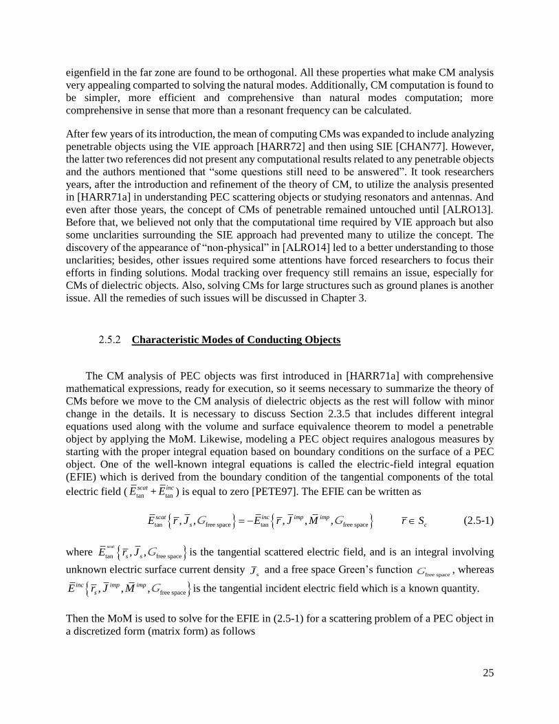
25
eigenfield in the far zone are found to be orthogonal. All these properties what make CM analysis
very appealing comparted to solving the natural modes. Additionally, CM computation is found to
be simpler, more efficient and comprehensive than natural modes computation; more
comprehensive in sense that more than a resonant frequency can be calculated.
After few years of its introduction, the mean of computing CMs was expanded to include analyzing
penetrable objects using the VIE approach [HARR72] and then using SIE [CHAN77]. However,
the latter two references did not present any computational results related to any penetrable objects
and the authors mentioned that “some questions still need to be answered”. It took researchers
years, after the introduction and refinement of the theory of CM, to utilize the analysis presented
in [HARR71a] in understanding PEC scattering objects or studying resonators and antennas. And
even after those years, the concept of CMs of penetrable remained untouched until [ALRO13].
Before that, we believed not only that the computational time required by VIE approach but also
some unclarities surrounding the SIE approach had prevented many to utilize the concept. The
discovery of the appearance of “non-physical” in [ALRO14] led to a better understanding to those
unclarities; besides, other issues required some attentions have forced researchers to focus their
efforts in finding solutions. Modal tracking over frequency still remains an issue, especially for
CMs of dielectric objects. Also, solving CMs for large structures such as ground planes is another
issue. All the remedies of such issues will be discussed in Chapter 3.
Characteristic Modes of Conducting Objects
The CM analysis of PEC objects was first introduced in [HARR71a] with comprehensive
mathematical expressions, ready for execution, so it seems necessary to summarize the theory of
CMs before we move to the CM analysis of dielectric objects as the rest will follow with minor
change in the details. It is necessary to discuss Section 2.3.5 that includes different integral
equations used along with the volume and surface equivalence theorem to model a penetrable
object by applying the MoM. Likewise, modeling a PEC object requires analogous measures by
starting with the proper integral equation based on boundary conditions on the surface of a PEC
object. One of the well-known integral equations is called the electric-field integral equation
(EFIE) which is derived from the boundary condition of the tangential components of the total
electric field ( tan
scatE + tan
incE ) is equal to zero [PETE97]. The EFIE can be written as
tan free space tan free space, , , , ,= − scat inc imp imp
s cE r J E r J M r SG G (2.5-1)
where tan free space, ,scat
s sE r J G is the tangential scattered electric field, and is an integral involving
unknown electric surface current density sJ and a free space Green’s function
free spaceG , whereas
free space, , ,inc imp imp
sE r J M G is the tangential incident electric field which is a known quantity.
Then the MoM is used to solve for the EFIE in (2.5-1) for a scattering problem of a PEC object in
a discretized form (matrix form) as follows

26
[ ][ ] [ ]incZ J V= (2.5-2)
where [ ]Z is the MoM impedance matrix, [ ]J is the column vector containing the unknown electric
current density on the structure, and [ ]incV is the excitation vector that is related to the incident
field. The details of the application of MoM and the transition from EFIE to the MoM matrix
equation in (2.5-2) is beyond the scope of dissertation but can be found in [PETE97]. Solving for
the unknowns in matrix equation above is considered a driven problem which is dependent on the
shape of the scatterer and the incident field specified. On the contrary, the characteristic modes
analysis is independent of any excitation (i.e. specifying an incident field) but dependent on
scattering object itself; hence, the MoM operator matrix ([Z]=[R]+j[X]) is then applied in the
computation of the generalized eigenvalue equation
[ ][ ] [ ][ ]=n n nX J R J (2.5-3)
where n and nJ are the eigenvalues and eigenvectors (eigencurrents), respectively. One can
clearly see that expression (2.5-3) does not have any dependency on any excitation term. Both [R]
and [X] must be symmetric in order to obtain real eigenvalues and eigenvectors due to the fact a
lossless case is considered [HARR71a]. The eigenvalues are defined as the ratio of the net stored
energy to the radiated power in the modes. So, an eigenvalue is equal to zero when the associated
mode is at resonance and equal to infinity (or large number) when the mode is non-radiating. The
eigenvalues can also be negative or positive indicating capacitive or inductive mode. The CM
eigencurrents are orthogonal which is an important property of the analysis, and such orthogonality
is mathematically verifiable via the following expressions [HARR71a]:
*[ ] [ ][[ ] [ ] [ ][[ ] = =T T
m n m n mnJ R J J R J (2.5-4a)
*[ ] [ ][[ ] [ ] [ ][[ ] = =T T
m n m n n mnJ X J J X J (2.5-4b)
( )*[ ] [ ][[ ] [ ] [ ][[ ] 1 = = +T T
m n m n n mnJ Z J J Z J j (2.5-4c)
where mn is the Kronecker delta.
0
1mn
m n
m n
=
= (2.5-5)
Note that the currents are normalized so individual modes radiate a power of 1 Watt. The CM
fields in the far zone (i.e. the sphere at infinity in the field’s integration) must also be orthogonal.
The following expressions [HARR71a] validate such property

27
1
m n mn
S
E E dS
= (2.5-6a)
and
1
m n mn
S
H H dS
= (2.5-6b)
where o
o
= is the free-space intrinsic impedance, and mE and mH are the far-zone
eigenfields due to mJ . Throughout the entire of this dissertation, expressions in (2.5-4) and (2.5-
6) are referred as the current and field orthogonality relationship, respectively, and they hold for
the CM analysis of PEC objects ( nJ related to electric surface current density).
The surface current density ( sJ ) can be expressed as a linear sum of the characteristic mode
currents ( nJ ) once an object is illuminated by an incident field.
0
=
=s n n
n
J J (2.5-7)
where n is the modal weighting coefficients of the nth mode and expressed as
tan,
1 1
i in n
n
n n
J E V
j j
= =
+ +. (2.5-8)
The modal excitation coefficients i
nV is expressed as the inner product of the CM eigencurrent
with the incident field. Therefore, how much of each of the characteristic modes is excited can be
determined for a given excitation. The quantity
1
1 =
+ n
MSj
(2.5-9)
is called the modal significance factor, which is part of expression (2.5-8). This quantity is equals
to any value from zero to unity; if a CM is resonant, then MS = 1. Due to the orthogonality
properties, any arbitrary surface current sJ and its fields ( E , H ) can be expressed as expansions
of the CM eigencurrent nJ and eigenfields ( nE , nH ), namely
1 1 1
i
n ns n n
n n n
V JJ J
j
= =
= =+
(2.5-10)

28
1 1 1
i
n nn n
n n n
V EE E
j
= =
= =+
(2.5-11)
and
1 1 1
i
n nn n
n n n
V HH H
j
= =
= =+
(2.5-12)
Characteristic Modes of Dielectric Objects
For CM computation of lossless dielectric objects, either the VIE approach or SIE approach can
be applied. The matrix form discussed in Section 2.4.5 related to the VIE approach applies to
general penetrable objects which can be magneto dielectric (d o and
d o ). The scope of
this dissertation is only concerned with dielectric objects (d o and
d o = ); hence, the MoM
matrix equation (2.3-5) reduces to = incZ J V since only eqJ is required. The application of
CM analysis is then straight forward as the case for PEC objects as discussed in the previous
section. The coupled integral equations (2.4-5) reduces to a single integral equation which is also
called EFIE; hence, the CM can be computed using expression (2.5-3) except that nJ represents
volumetric electric current density within the dielectric object.
Note that the presented formulations in both Section 2.4.5 A and B yields [C]=-[D] which allows
symmetrizing the MoM matrix for the characteristic modes computation which requires a
symmetric matrix in order to obtain real eigenvalues and eigencurrents for lossless materials. The
use of PMCHWT formulation is required in the CM analysis due to the fact that its matrix form
can be symmetrized, for a valid CM solution. Like VIE formulation, the dimensionless submatrices
[C] and [D] are equal with a negative sign; hence, the matrix can be symmetrized as follows
[CHAN77]:
inc
inc
VZ jC J
jC Y jM jI
=
(2.5-13)
Then, the generalized eigenvalue problem for solving the CMs then becomes
2 1
2 1
[ ] [ ] [ ] [ ] [ ] [ ]
[ ] [ ] [ ] [ ] [ ] [ ]
n n
nn n
X N J R N J
N B j M N G j M
=
(2.5-14)
where

29
[ ] [ ] [ ]Y G j B= + (2.5-15)
and
1 2[ ] [ ] [ ]j C N j N= + (2.5-16)
Expression (2.5-14) is the generalized eigenvalue equation which has the same form as (2.5-3).
Harrington and Chang presented the above approach of calculating CM of penetrable objects using
SIE formulation [CHAN77] for the first time; however, computational results on the proposed
approach with a contrast to the VIE approach were published in [ALRO14] for the first time. In
[ALRO13], it was found that an extra step is needed when CM is computed using SIE approach to
obtain the correct CMs; this will be discussed in Section 3.2.2.
Sub-Structure Characteristic Modes
aS
impJimpM
0 0( , )
PEC
Object A
PEC
Object B
bS
Figure 2.10: Two objects considered for the sub-structure CM analysis.
The analysis of sub-structure characteristic modes is considered a special case of the
characteristic modes analysis (conventional) which is discussed in the previous three sections;
basically, the modal solution is restricted to a set of CMs that is only associated with a portion of
an entire problem. For instance, consider object A and object B as shown in Figure 2.10 and assume
that one is only interested in finding the set of CM of object A in the presence of object B for two
possible reasons: either object B is electrically large which would result in too many significant
modes or object B is not altered in optimization process or similar. The discrete form of the EFIE
can then have its operator matrix [Z] partitioned such that it reads

30
[ ] [ ] [ ] [ ]
[ ] [ ] [ ] [ ]
AA AB A A
BA BB B B
Z Z J V
Z Z J V
=
(2.5-17)
Of course, two matrix equations can be written as follows
[ ][ ] [ ][ ] [ ]AA A AB B AZ J Z J V+ = (2.5-18)
and
[ ][ ] [ ][ ] [ ]BA A BB B BZ J Z J V+ = (2.5-19)
where sub-matrices [ ]AAZ and [ ]BBZ are the impedance matrices for Object A and B, and sub-
matrices [ ]ABZ and [ ]BAZ are coupling matrices between the two objects. The coefficients for the
electric surface current density AJ on Object A is contained in [ ]AJ , and those related to object B
is contained in [ ]BJ . If [ ]BV is assumed to be equal to zero (i.e. no excitation placed on object B),
then expression (2.5-17) becomes
1[ ] [ ][ ] [ ] [ ] [ ]−− =AA AB BB BA A AZ Z Z Z J V (2.5-20)
If the term 1[ ] [ ][ ] [ ]AA AB BB BAZ Z Z Z−− in (2.5-20) is called [ ]SUBZ , the MoM matrix equation can
be written as
[ ][ ] [ ]SUB A AZ J V= (2.5-21)
The surface current density on Object B can then be calculated using
1
B BB BA AJ Z Z J−
= − (2.5-22)
, given that the excitation restrictions above is considered [ETHI12]. In the latter reference, it is
shown that the restricted set of CMs of object A, namely the sub-structure CMs, in the presence of
object B can be solved using
[ ][ ] [ ][ ]SUB n n SUB nX J R J= (2.5-22)

31
Characteristic Modes of Dielectric Resonator Antennas
No attempt was made to publish computational results related to either approach after the
issue of [HARR72b] and [CHAN77] in which the CM analysis for penetrable objects using VIE-
approach and SIE-approach based on MoM was introduced until the first effort that was made to
break the silence and compute the CMs of penetrable objects for the first time [ALRO13], the flow
of literature work has started since then. In 2014, [ALRO14] and [CHEN14] discussed two
different approaches in calculating the CM of dielectric objects using PMCHWT (SIE)
formulation. Reference [ALRO14] introduced the concept discussed in 3.2.2; whereas
eigencurrents are solved based on J-only or M-only CMs by rearranging the MoM solution matrix
similar to the way it is done in expression (2.5-21) in [CHEN14]. The latter reference claims that
one can obtain the same CMs as [CHAN77] however, we could not verify such claim. In
[BERN14], a rectangular DRA to be designed at 60 GHz was studied for its resonances using VIE-
approach CM analysis, and similarly, a 60-GHz coplanar-waveguide-fed slot-coupled rectangular
DRA design was designed by studying CM analysis, except that a similar approach to the sub-
structure CM was used. The modal behavior of a rectangular DRA placed on same size substrate
was studied in [GUAN16] using the approach proposed in [CHEN14]. For the first time, the Q-
factor was calculated using the CM currents at any frequency (i.e. not just at resonance) for a
cylindrical DRA in [YANG17]; yet, this calculation only valid when VIE-approach is used in
calculating CMs. A more efficient CM calculation based on VIE approach was proposed in
[WU17] by employing interpolation technique; the proposed technique was applied on rectangular
DRA with homogenous medium and stacked rectangular DRA and found to be successful. Still,
the SIE approach is found to be more computationally efficient even though it suffers from non-
physical modes.
All the above CM works on dielectric resonator only used CM analysis tool to study their modal
behavior and determining the modal resonances; however, there was no direct involvement of CM
in determining dimensions or feed placement
WIRELESS COMMUNICATION SYSTEM REQUIREMENTS
Wireless Communication systems have certain expectations and specifications to operate
properly and reliably depending on the condition of channel environment and parameters. Some
of those specifications are namely the signal-to-noise ratio (SNR), data rate, channel capacity, and
bandwidth. Besides reliability and efficiency, high data rate is required in nowadays’ technology
and very vital due to the increase of data transfer such as video streaming and high-speed internet
such as the fifth generation (5G) network. The key is high data rate which can be improved by
increasing either the transmit power, bandwidth or both. On the other hand, diversity techniques
can increase the channel capacity and hence the data rate. Increasing the bandwidth at which the
data is transferred technically leads to higher data rate, and that is a simple and common problem.
However, bandwidth limitation in certain bands restricts one from extending the operational
bandwidth, and for example, that is why we see multiple bands for cellular networks including for
4G and long-term evolution (LTE). Similarly, there can also be restriction on the transmit power
level whether by the federal communication commission (FCC) or even the system itself.

32
Therefore, restrictions on bandwidth and transmit power have made many to consider diversity
which also can increase reliability and/or data rate: reliability through space-time diversity
techniques and channel capacity increase through spatial diversity techniques [GORO03]. One of
the diversity techniques is to integrate multiple-input multiple-output (MIMO) antenna whether as
a transmitter or receiver end or actually both, and this relatively new technology is gaining more
ground for future applications such as 5G networks which require higher channel capacity and data
rate. Capacity channel is dependent on the number of antennas in your system expressed as follows
2log (1 )Tx RxC BW M M SNR= + (2.6-1)
where Tx RxM and M are the number of antennas in the transmitter and receiver side, respectively.
Note that the channel capacity is proportional to the logarithmic of the number of antennas in both
sides, so there is a clear growth in the channel capacity by simply increasing the number of
antennas. On the other hand, diversity using MIMO can be used to improve reliability by sending
the same signal using the multiple antennas form and sometimes with some type of delay; that way
the signal sent is found more reliable when it reaches the other side. The design side of MIMO
antennas is simply by having an antenna with multiple ports operating at the same frequency with
high isolation between the ports which is measured by the envelope correlation coefficient (ECC).
The ECC quantity for a two-port MIMO antenna can be expressed in terms of the S-parameters of
the two ports [ROSE05] as follows,
* * 2
11 12 21 22
2 2 2 2
11 21 22 12
| |
(1 )(1 )
S S S SECC
S S S S
+=
− − − − (2.6-2)
This quantity determines how well uncorrelated the ports are, so the minimum ECC value over
than bandwidth for MIMO antennas is 0.5; however, a much lower value might be required based
on the system in use.
It has been clear bandwidth, channel capacity, and SNR are some of the requirements that would
depend on the antenna’s (or multiple antennas’) requirements. And since the antenna is the front-
end device for any wireless communication; if the antenna fails to realize such requirements, the
whole communication system would fail, no matter how perfectly designed the rest of the
communication system is. In Chapter 5, the most wanted three requirements in for an improved
performance in wireless communication systems are presented and addressed through designing
antennas for an optimized bandwidth, MIMO application, and restriction on antenna size and
pattern application. The latter requirement is also important in wireless communication
applications in which a limited space for the antenna is essential to keep gadgets as compact as
possible. Finally, pattern directivity can play a role in lowering SNR, as the system avoid
transmitting and/or receiving undesired signal or transmitting in unserviceable directions.

33
ADDITIVE MANUFACTURING
Additive manufacturing technology has been booming, and the name comes from building a
shape by adding ultrathin layers of materials one by one. Additive manufacturing with the use of
three-dimensional (3D) printing technology has evolved tremendously, and we have seen more
interest in using such technology in many applications. Building simple or complex shapes using
traditional techniques is something from the past; nowadays, a wide range of 3D printing
technology is available for hobbyists and small entrepreneurs to commercial and giant
manufacturers. Nowadays almost everything from machinery components such as jets, cars, and
space shuttles to little things like dolls are being made by 3-D printers; anything one can think of
may be printed with a high resolution up to 20 microns provided that the AutoCAD model is
available. Additive manufacturing has been a very important subject in the EM and communication
community because it offers a great deal of ease in fabricating some complex shaped parts; and
printing antennas is one of them. The conventional fabrication methods of some of the complicated
shaped antennas is time consuming, expensive, and possibly inconsistent. While, 3-D printers offer
just the opposite, so the combinations of cost effectiveness, time efficiency, and precision have
made the antenna of shape synthesis possible and more attractive. A variety of materials, both
dielectric and metal, are available for 3D printers such as acrylonitrile butadiene styrene (ABS)
plastic, poly lactic acid (PLA) nylon, carbon, nylon, bronze fill, glass filled polyamide, wax,
photopolymers, silver, titanium, steel, and polycarbonate. The three main type of 3D printer
technology used nowadays are the SLS (selective laser sintering), FDM (fused deposition
modeling) & SLA (stereolithography), and the most common one used off shelf is the FDM.
Even though fabricating dielectric resonators using 3D printers is not a novel work [NAYE14]
[QU14], the work of DRA shape synthesis proposed in this dissertation heavily relied on the 3-D
printing technology due to the final complex shapes as a result of geometrical control, discussed
in Section 4.3. Without such technology, this work would have been more complicated by dealing
only with conventional methods. In this work, two 3D printers operate based on FDM technology
which a simple deposition of filament after the material is heated through an extruder builds a layer
after another. The learning factory facility on campus of Pennsylvania State University offers few
selection of 3-D printers, and one of them is the “Stratasys uPrint SE” which uses ABS material
(ABS plus p430 ivory). The other printer made by QIDI Technology and called X Pro is designed
for ABS and PLA material with open filament12, it is one of the popular off-the-shelve 3D printers.
It was purchased for this project since samples of ABS filaments with various dielectric constants
were received from PREMIX group and could not be used on any 3D printer on campus. The
filaments from PREMIX group was made of ABS and the material electrical properties were made
available. In addition, they can be used in any 3-D printer that is compatible with ABS filament of
1.75 mm diameter. The advantage of those filaments is that their dielectric constant ranges from 3
to 10 with a tangent loss of 0.004. This is a huge development in the field of 3-D printing since the
dielectric constant of the widely available ABS, PLA, and polymer is around 3. The different
material used in the 3D printers will be discussed in the following section, as well.
12 Any branded filament of 1.75 mm diameter can be used.

34
CHARACTERIZATION OF DIELECTRIC MATERIAL
ELECTRICAL PROPERTIES
Our interest in shaping dielectric resonator antenna has made us to explore several 3-D printers
and their different materials. The most common dielectric material used in today’s 3-D printing
technology is ABS and PLA. Unfortunately, many of these materials are not characterized in terms
of electrical properties such as the permittivity and loss tangent as a function frequency which play
an important role in radio frequency (RF) and microwave designs. However, measuring the
electrical properties of unknown material is possible given that the material is not too lossy. There
are few methods to characterize either dielectric or magnetic material using methods such as the
perturbation technique, optical techniques, transmission line technique, and exact resonance
method; however, the latter were found to be provide an accuracy of ±0.1% [HAKK60]. The exact
resonance method is also called dielectric resonator method which measures inductive capacities
of circular disk, made of any material to be measured, which is inserted in the gap of a cavity of
known dimensions. The dielectric constant r and loss tangent tan are determined by measuring
the resonant frequency and Q-factor. The physical size of circular disk dielectric resonator is
determined based on the resonant frequency of the dominant mode (TE) with taking an initial guess
of the dielectric constant. The physical experiment of the material characterization involved a
vector network analyzer (VNA) and a similar instrument shown in Figure 2.11 except that two
probes connected to the VNA are used instead of the waveguide. The transmission coefficient |S21|
between the two probes via the circular disk is then measured, and if the cavity is resonating around
the design frequency at which the dominant mode is excited, then a peak13 with a relatively higher
|S21| than any other peak should be spotted. The peak is indicative that the signal from the probe is
transmitted and receive by one port from the other is allowed to travel due to the resonance.
Depending on how close the initial guess of the dielectric constant to the actual value, the peak
should lie approximately around the design resonant frequency, and unlike the other peaks, it
should not be stationary and should shift to lower frequencies as the conducting plates14 are lifted
away from the disk since the disk becomes electrically larger as the plates moving away. Once
the resonant frequency is identified along with physical dimension of the disk, then the actual
dielectric constant can be calculated precisely. Then the tangent loss can be simply determined
from calculating the Q-factor that is measured using the 3-dB bandwidth level of the peak. All the
necessary equations to determine the physical dimensions of the disk for a rough resonant
frequency and r , and then the actual r and tangent loss based on the measured resonant
frequency and Q-factor were coded in a software provided by the material research institute (MRI).
The dielectric materials mentioned in the previous section were characterized using the exact
resonance method in the MRI lab. Even though the electrical properties of the PREMIX filament
samples are made known, a confirmation of their accuracy was desired. Table 2-2 lists all the
material characterization
13 Only if the dominant mode is excited. If higher modes are excited, then multiple peaks might merge. 14 During the measurement, the conducting plates sit tight against the top and bottom of the disk.

35
Figure 2.11: Instrument used in for material characterization using exact resonance method [HAKK60].
measurement performed for material obtained from the Stratasys, PREMIX, and QIDI Tech. As
mentioned before, the dielectric constant of most PLA and ABS are around 3, and it is well known
that PLA is more lossy, as the tan indicates in the table. The measurement of dielectric constant
of PREMIX filament are somewhat off, but the measured tan are less than the one reported.
Table 2-2: Material characterization parameters (calculation and measurement) for different materials.
Type
of
Material
Initial
r
Disk
Diameter
x Height
(mm)
Calculated
Resonant
Frequency
(GHz)
Measured
Resonant
Frequency
(GHz)
Measured
3-dB
Bandwidth
(MHz)
Calculated
r
Calculated tan
ABS P430 3 34.7x10.2 10 9.8 57 2.99 0.0059
PREMIX 6.4 6.4 19.85x9.9 8.18 7.975 25.5 6.87 0.0032
PREMIX 7.5 7.5 10.1x10.0 10.81 10.44 30.6 7.99 0.0031
PREMIX 10 10 10.5x10.2 9.45 9.124 25.0 9.93 0.0028
ABS QIDI
Tech.
3 34.6x9.6 10 9.90 49.0 3.28 0.0049
PLA QIDI
Tech.
3 34.8x9.95 10 9.93 50.0 3.07 0.0098

36
All the samples listed in Table 2-2 were printed with 100% density (solid). 3D printing with ABS
materials requires some special attentions: the extruder temperature should always be set between
235 – 245 degrees Celsius, whereas the printing bed should be heated to 100 degrees Celsius. The
travel speed was set to 60 mm/s, and the layer height was set to 0.2 mm. Printing pattern for the
inner wall are made of lines, and the support for the whole structure was a grid. These settings are
very important for a successful printing with ABS material. Additionally, an enclosure for the 3-
D printer is highly recommended for printing the ABS material, whereas 3D printing area should
be completely ventilated when PLA materials are used. The setting for PLA material are quite
different since the extruder temperature is usually set between 220-230 degrees and some faster
travel time can be set. No heated bed is required when PLA is in use. Finally, all the filament used
in the sample and fabrication has a diameter of 1.75 mm, and the extruder diameter is 0.4 mm.
CONCLUSIONS
Some requirements for antenna performance for wireless communication systems were
summarized to be applied for DRA shape synthesis as the main contribution of this dissertation. It
was shown the DRAs have multiple advantages over many other antenna types, and these
advantages lie in having a superior radiation efficiency in contrast to those antennas made of
conductors, the possibility of compact design, excitation of modes with different field
distributions, the ease and the flexibility of selecting a feeding structure, and finally the low cost
of fabrication, and finally the ease of integrating to a circuit printed boards. The wide selection of
dielectric materials provides antenna designers more freedom in the design procedure since each
material has an effect on the electrical size and field confinement within the DRA. Then, important
numerical tools of analyzing DRAs, namely the CM analysis, and it is appealing properties were
discussed in details to ensure laying a solid foundation to rely on when building the shaping
synthesis process is performed. A literature review on different works on DRAs with
unconventional shapes were conducted to comprehend what more needs to be done when the shape
synthesis on DRAs is applied using the characteristic modes. Additionally, a review on the analysis
of characteristic modes was performed to fully understand what can be applicable for the shaping
process or extending concepts that can be important for future work. The appealing CM properties
which lies in excitation independency and current and field orthogonality have made it possible to
relax restrictions on the shaping process by not considering any feed point as the initial analysis.
This will be discussed more in details in the following chapters. Then, the use of 3D printers and
the variety of materials such ABS with different permittivities with low losses has made it possible
to precisely fabricate complicated DRA shapes in timely manner with keeping the cost low.
Finally, it was also shown that the material properties of dielectric filaments commonly used in
FDM 3D printers can be easily characterized as long as they are not lossy.

37
CHAPTER 3: A CHARACTERISTIC MODE
INVESTIGATION OF DIELECTRIC
RESONATOR ANTENNAS
INTRODUCTION
The DRA antenna shape synthesis method to be developed in Chapters 4 and 5 utilizes
characteristic mode concepts. The determination of the characteristic modes of dielectric objects
has been fraught with difficulties, and there have been uncertainties in the literature as to precisely
what was being computed. A number of aspects of characteristic mode theory therefore had to be
investigated and repaired before the shape synthesis work could proceed. These are all described
in Section 3.2, which ends with a discussion of remnant controversies but explains why these do
not influence the work of this dissertation. Section 3.3 notes the difference between the natural
modes of an object and its characteristic modes. It also states why, at least from a computational
electromagnetics point of view, characteristic modes are preferred in the antenna shape synthesis
work that is the prime goal of the dissertation. Section 3.4 makes a brief foray into the theory of
characteristic modes analysis of some conventional dielectric resonator antennas in order to
confirm some simple common-sense understandings of such antennas from a characteristic mode
viewpoint. Section 3.5 concludes the chapter.
EXTENSIONS OF SOME BASIC CONCEPTS IN CHARACTERISTIC
MODE THEORY
Initial Remarks
Section 3.2 catalogues some contributions to basic CM theory and computation that was done
while undertaking the work of this dissertation, whether it is actually used in later chapters or not.
Non-Physical Modes – Comments on Earlier Work
Section 2.5 mentioned that either VIE- or SIE-based formulations could be used to determine
the CMs of dielectric objects. However, the SIE approach is preferable (especially for the shape
synthesis work to be described in Chapters 4 and 5) because of its very significantly lower
computational burden compared to the VIE approach. It was then pointed out that, in work done
prior to the present dissertation, this author had identified [ALRO14] non-physical modes that are
obtruded when the SIE route is followed and showed how these could be identified and discarded.
This has made the use of the SIE in finding the CMs of dielectric objects reliable. Indeed, the
approach has since been incorporated in the commercial computational electromagnetics software
package [FEKO].

38
Mode Tracking
Modal tracking has been always an issue in CM analysis no matter which formulation is used
in the calculation, and it is very important step to observe the modal behavior over a frequency
sweep. Linking modes from one frequency step to the next one is basically what modal tracking is
all about; since solving eigenvalue equation is dependent on the MoM solution matrix at every
frequency step in any desired range, the indices of the yielded eigenvalues and their corresponding
eigenvectors shuffle around at each frequency step due to the change in the magnitude of
eigenvalues over frequency. A very large negative or positive (i.e. capacitive or inductive mode)
CM eigenvalue, which is indicative of being insignificant, eventually becomes smaller and goes
through zero (i.e. resonance) as the structure becomes electrically large, and then the value climbs
up in magnitude again. As a result, this particular mode is assigned an index either based on the
rank of its magnitude in ascending order for the very first frequency step in the calculation or the
occurrence of it resonance, but the index should remain the same throughout the frequency range.
Thus, the model tracking ensures assigning the indices in one frequency step based on the previous
one and so on.
In the literature, several tracking techniques have been proposed to combat this modal tracking
issues. References [LUDI14, RAIN12, CAPE11, AKKE05] are some of the earlier work on modal
tracking for which these techniques mainly rely on the process of the eigencurrent correlation. A
different approach in modal tracking was implemented in [MIER15] by using the far-field pattern
correlation, instead. All these methods work quite well, especially [RAIN12], for tracking CMs of
PEC objects or dielectric objects calculated based on VIE approach. But unfortunately, some of
these methods cannot be completely reliable for tracking modes of dielectric objects calculated
using SIE approach due to the presence of non-physical modes in the solution. The existence of
eigenvalues of non-physical modes and their corresponding eigencurrents can be troubling as the
eigencurrent can be somewhat well correlated to some physical modes; as a result, relying solely
on the eigencurrent correlation may cause modal mismatch. Therefore, a hybrid modal tracking
has been introduced for the first time; both the eigencurrent correlation and field orthogonality
check are performed. The field orthogonality is a necessary step to filter out the non-physical
modes to prevent mixing up physical and non-physical modes during the tracking process and
wasting unnecessary resources during the eigencurrent correlation process.
In the proposed hybrid tracking algorithm, a number of lowest physical CMs to be tracked must
be specified, and the CM tracking is performed over frequencies , 1,2,...,qf where q Q= , where Q
is the number of frequency steps. We refer to Section 2.5.3 B since it is concerned with SIE-
approach in calculating CMs, so the eigenvalues n and the eigenvector [ ] [ ], [ ]T
n n nF J j M= are
calculated at each qf . Both n and nF are frequency dependent, so we denote them as ( )n qf and
[ ( )]n qF f . The value of number of unknowns, N, in the solution of the MoM is kept fixed for all
frequency steps by fixing mesh size which is based on the highest frequency. The eigenvalues at
each frequency iteration are sorted in ascending order in a column vector
1 2( ) , ( ) ,..., ( )T
q q N qf f f , for n =1,2, …, N, at q-th frequency iteration. The modal tracking
are then performed as follows:

39
1) The number of desired physical CMs to be tracked maxA is to be defined. At the first iteration
1f , 1( )n f and 1[ ( )]nF f are calculated for n=1, 2,…,N. And then the quantity
1
1 P ( ) nn n n
S
f E E dS
= (3.2-1)
, which is related to the field orthogonality, is to be computed for n=1,2,…,M. The value M is the
number of modes computed using expression (3.2-1), and within these modes are maxA modes that
satisfies the condition 1P ( )nn f . The threshold value is recommended to be 0.2. Only
consider the latter modes 1( )n f and 1[ ( )]nF f for n=1,2, …, maxA .
2) At q=2 iteration, 2( )n f and 2[ ( )]nF f are calculated for n=1,2,…,N. Then, 2 P ( )nn f is
computed in order to find maxA to find a set of 2( )p f and 2[ ( )]pF f for p=1,2, …, maxA .
Then the current correlation between 2[ ( )]pF f and 1[ ( )]nF f are performed for m =1,2,…,
maxA and p=1,2, …, maxA based on [RAIN12].
3) The above steps are repeated for q= 3,4,…,Q.
We simply cannot just consider the physical modes only in the modal tracking since we have found
out that where the non-physical and physical mode intersect at certain frequencies, the value of Pnn
can drop from 1 to 0.2 or so. Thus, of 0.2 is recommended, to not exclude any physical modes.
This is to do with numerical issue, and backtracking can be used in the proposed method if the
wrong mode is assigned since P ( )nn nf may fall below the threshold, which seldomly happens.
Away from the intersection point, the physical mode can be identified in the following iteration
because the corresponding P ( )nn nf should climb up again. In Figure 3.1, a comparison between the
tracked CMs using [RAIN12] methods without a manual intervention, and the current proposed
method for the same geometry discussed in the previous section. Clearly, a more properly tracking
was achieved especially for the dominant mode.

40
Figure 3.1: the colored solid lines represents those modes tracked using the proposed method whereas the
circles represents the modes tracked using the technique in [RAIN12].
The hybrid tracking method have been then enhanced for more efficient computational time and
reliable tracking. In addition, some important findings about tracking CM calculated based on SIE
approach is discussed in this section. The first improvement is to increase the value of from 0.2
to 0.5 in order to exclude non-physical modes in the tracking process since their corresponding
P ( )nn qf should not exceed 0.5 even though P ( )nn qf of physical modes may fall below 0.5. The
starting frequency iteration should be always below the first resonance because the intersection
between physician and non-physical modes is unlikely to occur and the all the desired physical
modes are more detectable since P ( ) 1nn nf ,. By applying these improvements and changes to the
previously proposed method, the steps for the enhanced modal tracking are as follows
1) At 1f , calculate 1P ( )nn f for every CM (ordered in ascending order) and only accept those
with 1P ( )nn f > 0.5 until the value of maxA is reached. This step ensures excluding any no non-
physical mode, and this is the first improvement from the previous method.
2) When q > 1, calculate the correlation between the eigencurrents found in 1qf − (i.e. tracked
eigencurrent) and all the eigencurrents found in the current iteration q. Link those eigencurrent at
q to those already tracked through selecting the maximum correlation with ensuring that
correlation value is greater than 1/3, and then examine P ( )nn qf of those selected modes at q and
confirm that their corresponding P ( )nn qf is greater than 0.5. This step was modified to make the
computation more efficient since the number of eigenfields calculated in this step is lowered
compared to the previous proposed technique.

41
3) If one of the previously-tracked modes at1qf − is not being assigned in step 2, then find two
or three modes with the highest correlation as long it is higher than 1/3, and the mode with the
highest P ( )nn qf is then assigned to mode at 1qf −. In this step, the condition of 0.2 < P ( )nn nf < 0.5
must be fulfilled. This current step prevents unnecessary backtracking which may cause confusion
in the tracking procedure and consume more time.
All the above steps are added to the previously-proposed hybrid modal tracking, and these
improvements ensure a more accurate CM tracking and more efficient computation. In addition to
those steps, further measures can be taken for a smoother and more reliable tracking, and that is to
do with the MoM solution mesh size. It was observed that a better eigencurrent correlation and
Pnn values as a function of frequency can be achieved by using a finer mesh15. Provided that the
frequency separation is not large, the theoretical values for both quantities should be close to unity
between two identical modes at two different frequency points since the change in the modal
behavior over frequency is considerably slow. However, due to numerical discrepancies, those
values can drop drastically for the identical CMs. For the same example considered above, one can
see that not only the eigenvalue of the dominant CM (physical) is converging, but also how smooth
the curve becomes as the number of expansion functions are increased, as depicted in Figure 3.2.
This is due to the fact that both Pnn and correlation values of the dominant mode were improved as
shown in Figure 3.3 and Figure 3.4, respectively. Thus, increasing the mesh size is a remedy for
modal tracking issue and is more important than increasing the number of frequency steps which
is an approach proposed in the literature. Unfortunately, this comes at the expense of
computational time; however, it saves one the trouble of having improper CM tracking.
Figure 3.2: The eigenvalue of the dominant physical CM of the notched DRA shown as a function of mesh size.
15 By increasing the number of expansion functions (or number of unknowns).

42
Figure 3.3: The quantity of Pnn of the dominant physical mode, associated with Figure 3.2, at every frequency
iteration as a function of mesh size.
Figure 3.4: The quantity of the correlation values between the dominant mode, associated with Figure 3.2, at
every frequency iteration as a function of mesh size.

43
Sub-structure Modes – Broadened Concept
The sub-structure mode concept was described in Section 2.5.4, in the manner of [ETHI12].
In this section we will show that a more general interpretation of the sub-structure characteristic
mode concept is possible, and that an assumption made in [ETHI12] is not actually needed. In the
interests of continuity, lest the reader have to page back and forth between Section 2.5.4 and this
one, some of what is provided will be repeated here.
We suppose we have a perfectly conducting (PEC) structure, composed of two objects or parts, as
shown in Figure 3.5, with 0 A BS S S= . The electromagnetic scattering problem related to this
structure can be modelled using an electric field integral equation (EFIE)
tan tan 0( ) ( )scat incE r E r r S= − (3.2-2)
for the surface electric current density sJ everywhere on the structure, with tan
scat
sE J= Z , and
integral operator ...Z incorporating a free space Green’s function as the kernel of the IE. The
EFIE can be solved using the method of moments [HARR 68]. Expansion and weighting functions
are distributed over the PEC surface 0S (on both constituent objects), and the matrix equation
fs fs[ ][ ] [ ]Z J V= (3.2-3)
formed as the discretized version of the EFIE, where the symbols have their usual meanings. The
superscript “fs” explicitly recognizes use of the “free-space” Green’s function. It is assumed that
a Galerkin approach is used, so that fs[ ]Z is symmetrical. In practice, even if this is not the case,
the matrix operator will usually be sufficiently close to being symmetric for the purposes of
characteristic mode computation if sufficiently fine meshing is used.
It is possible – and we will need this in the definition of the sub-structure characteristic mode
below – to purposefully view the structure in Figure 3.5 as consisting of two portions, Objects A
and B, with distinct expansion function subsets located on these two portions. We can then
partition the moment method matrix equation to read
fs fs fs
AA AB A
fs fs fs
BA BB B
[ ][ ] [ ] [ ]
[ ][ ] [ ] [ ]
A
B
JZ Z V
JZ Z V
=
(3.2-4)
This does not alter the scattering problem in any way. We will call (3.2-3) and (3.2-4) the primary
moment method formulation equations, for reasons that will be clear shortly.

44
It is possible to find the characteristic modes (CMs) of the complete structure as the solutions of
the matrix eigenvalue problem
[ ][ ] [ ][ ]fs fs fs
n n nX J R J= (3.2-5)
with [ ] [ ] [ ]fs fs fsZ R j X= + . We have written these eigenvalues as fs
n to indicate that they have
been found using matrix operator fs[ ]Z as the starting point. The far-zone CM eigenfields can be
found for each CM eigencurrent [ ]nJ , the latter being real (equiphase). As in Section 2.5.4, we
will refer to these are the conventional CMs of the complete PEC structure.
( ), ( )E r H r
0 0( , )
Object A
Object B
Figure 3.5: Perfectly conducting (PEC) structure consisting of two parts.
It is shown in [HARR71a] that the CM eigencurrents and eigenfields satisfy certain useful
orthogonality relations. In terms of the notation being used here, these are
[ ] [ ]
[ ] [ ][ ] [ ][ ] [ ]
H
An AnH fs fs
n n mn
Bn Bn
J JJ R J R
J J
= =
(3.2-
6)
[ ] [ ]
[ ] [X ][ ] [X ][ ] [ ]
H
An AnH fs fs fs
n n n mn
Bn Bn
J JJ J
J J
= =
(3.2-7)
and
*
0
1m n mn
S
E E dS
= (3.2-8)

45
where the superscript “H” signifies the transpose conjugate operation and 0 0 0/ = . Quantity
nE is the far-zone field due to eigencurrent [ ]nJ , the integral being taken over the sphere at infinity.
The fields are also point symmetric [GARB82].
We can next define the broadened sub-structure CM concept. In order to do this, we manipulate
matrix equation (3.2-4) into the two equations
1
fs fs fs 1 fs fs fs fs fs
AA AB BB BA A AB BB B[ ] [ ][ ] [ ] [ ] [ ] [ ]AZ Z Z Z J V Z Z V−
− − = − (3.2-9)
and
1 1
fs fs fs fs
BB BA BB BB AJ Z Z J Z V− −
= − + (3.2-10)
In (3.2-9), we can write
fs fs fs 1 fs
AA AB BB BA sub[ ] [ ][ ] [ ] [ ]Z Z Z Z Z−− = (3.2-11)
and obtain the sub-structure CMs of Object A in the presence of Object B from eigenvalue problem
[ ][ ] [ ][ ]Asub sub Asub
sub n n sub nX J R J= (3.2-12)
with sub-structure eigenvalues sub
n different from those fs
n of the conventional CMs, and
[ ] [ ] [ ]sub sub subZ R j X= + . Note that the set of sub
n are not a subset of the set of fs
n .
The [ ]Asub
nJ are the sub-structure eigencurrents on Object A in the presence of Object B. In order
to find the eigenfields due to sub-structure eigencurrents [ ]Asub
nJ we must first find the “secondary”
currents sec[ ]B
nJ on Object B. This is a separate driven problem. We must view [ ]Asub
nJ as an
impressed current density (with Object A absent) that illuminates Object B and use a moment
method formulation (which we will call the secondary moment method formulation) to find sec[ ]B
nJ . The elements of fs
BAZ in the primary formulation are of the form
, ( ) ( )dS
B
ij j i
S
Z E r J r J r= . Here , ( )jE r J r would be the electric field at r due to the j-th
expansion function ( )jJ r , which is on Object A, whereas ( )iJ r is the i-th weighting function,
which is on Object B. Now the matrix equation for the secondary problem would be of the form
fs sec sec
BB [ ] [V ]B
n BZ J = (3.2-13)
We write sec[V ]B because it is the excitation with
Asub
nJ as the impressed current and is not the same
as in primary formulation (3.2-4). If we use the same expansion functions on Object B for both the
primary and secondary problems then fs
BBZ is the same in the two problems. The elements of

46
sec[V ]B in the secondary formulation will be of the form , ( ) ( )dS
B
inc Asub
n i
S
E r J r J r− , where
, ( )inc Asub
nE r J r would be the electric field at r due to Asub
nJ viewed as an impressed current
density. Of course, we have ( )Asub
nJ r described in the form of expansion functions and a set of
coefficients. Thus, the expression for sec[V ]B in fact reduces to
sec fs Asub
BA[V ] [ ]B nZ J = − (3.2-14)
If we substitute this into (3.2-13) the latter becomes
fs ec fs Asub
BB BA[ ] [ ]B
n nZ J Z J = − (3.2-15)
which can be rewritten as 1
Bsec fs fs Asub
BB BA[ ] [ ]n nJ Z Z J−
= − (3.2-16)
Thus, it turns out that we already have all the matrix information needed for the secondary moment
method formulation from the primary formulation. Expression (3.2-16) just happens to be the same
as (3.2-10) with fs
B [0]V = , but has nothing to do with fs
BV or fs
AV of the primary problem.
The sub-structure CMs do not depend on fs
BV or fs
AV in any way, as expected in CM
formulations. The sub-structure formulation does not require that “we put fs
B [0]V = ” (as was
thought16 necessary in [ETHI12]), even though the resulting expression is the same. The sub-
structure CM field nE is the superposition of the fields due to Asub
nJ and secB
nJ .
At this point we have not yet shown that the sub-structure operator matrix [ ]subZ in (3.2-11) is
symmetrical, which is key to any CM formulation. However, it is common knowledge that in
Galerkin moment method formulations fs
AA[ ]Z and fs
BB[ ]Z are symmetrical, and that fs fs
AB BA[ ] [ ]TZ Z=
. Thus fs 1
BB[ ]Z − is also symmetrical. The identity for the transpose of a valid
product of any three matrices [NOBL69], namely ( )[ ][ ][ ] [ ] [ ] [ ]T T T TA B C C B A= , ensures that
( ) ( )fs fs 1 fs fs fs 1 fs fs fs 1 fs
AB BB BA BA BB AB AB BB BA[ ][ ] [ ] [ ] [ ] [ ] [ ][ ] [ ]T T
T TZ Z Z Z Z Z Z Z Z− − −= = (3.2-17)
and hence fs fs 1 fs
AB BB BA[ ][ ] [ ]Z Z Z− is symmetrical. This in turn implies that [ ]subZ , being the sum of two
symmetrical matrices, is itself symmetrical. Thus, from the eigenvalue problem (3.2-12) we know
16 The sub-structure characteristic mode concept introduced [ETHI12] was intended to deal with the restricted type of
problem discussed in the reference, and hence the less general form was satisfactory.

47
that [ ]Asub
nJ will be real (equiphase). In general, Bsec[ ]nJ can be complex. Thus, the fields of the
sub-structure CMs will not necessarily be point symmetric.
After further extending the sub-structure CM ideas in Section 3.2.6, the orthogonality properties
of these modes are stated, proven and discussed in Section 3.2.7.
Sub-Structure Modes – Equivalence to Modes Determined from Integral
Equations with Modified Green’s Functions
Referring once more to Figure 3.5, suppose we know the modified Green’s function17 which
can be used to determine the field in all of space for an arbitrary electric current density distribution
in the presence of Object B, and use it to derive an EFIE for the current density on Object A. In
the associated moment method formulation, the expressions for the impedance matrix and
excitation vector now involve the appropriate modified Green’s function and so are not the same
as when the free-space Green’s function is used. We thus write the matrix equation as
md md[ ][ ] [ ]AZ J V= (3.2-18)
with “md” indicating use of the “modified” Green’s function in the EFIE. The eigenvalues of the
eigenvalue problem [ ][ ] [ ][ ]md A CM md An n nX J R J= can be denoted md[ ]CM
n Z . We might call these the
modified CMs of Object A in the presence of Object B. This approach has been used in [CABE07]
implicitly in many references that discuss the characteristic mode properties of microstrip patches
on lossless substrates18. The [ ]AnJ are real, as expected, and the usual orthogonality properties are
satisfied. Since we can find the eigenfields using the modified Green’s function we need never
concern ourselves with the current density on Object B. However, if we use the eigenfields along
with the boundary condition on the tangential magnetic field to actually find [ ]BnJ , we observe that
it is in general complex. The eigenfields are not point symmetric.
Expression (3.2-18) is a matrix equation for the unknown current density AJ on Object A. The
influence of Object B is contained in matrix sub[ ]Z . The excitation term has altered to one that
depends on the illumination of both Object A and Object B. Both (3.2-2) and (3.2-18) are matrix
equations for the same unknown AJ on Object A, arrived at in two different ways. Thus, sub-
structure characteristic modes and modified characteristic modes are one and the same thing. The
sub-structure mode is effectively using a discrete form of the modified Green’s function that
accounts for the presence of Object B, although this Green’s function is not generated explicitly.
This makes the sub-structure CM concept a very versatile one.
17 As opposed to the free-space Green’s function. 18 The Green’s function for impressed electric of magnetic current densities radiating in the presence of a grounded
dielectric layer of finite thickness but infinite extent is well-known.

48
The results in Figure 3.6 demonstrate this numerically, in that the sub-structure modes for a strip
dipole (Object A) above a large groundplane (Object B) are virtually identical to the modified
modes for the same strip dipole above an infinite groundplane. The relevant dimensions of the
objects are summarised in Table 3-1. The computations were done using the FEKO code [FEKO].
The advantage of FEKO over other commercially available codes that allow use of the method of
moments is that it allows one to extract the moment method matrix. We then use this matrix to
perform all the various matrix manipulations and eigen analyses “offline” using MATLAB
software. Thereafter the CM currents (namely their coefficients) are sent back to FEKO, which is
then able to find the CM fields. The triangular mesh on the strip dipole was such that no expansion
function triangle edge length was more than 2.15 mm (λ/70 at 2 GHz, a very fine mesh) and that
on the finite sized groundplanes such that no triangle edge was larger than 15 mm (λ/10 at 2 GHz,
an average mesh).
Table 3-1: Dimensions of the dipole, small groundplane, and large ground plane
Dipole Length 75mmdL = and width 2.5mmdW =
Small
Groundplane
5g dW W= and 1.5g dL L=
Large
Groundplane
40g dW W= and 5g dL L=
Modified Green’s functions (especially those of direct use in antenna problems) are scarce. They
can only be found in closed form when the object in whose presence the particular source is
radiating has a boundary corresponding to a constant coordinate surface of a known coordinate
system, so that the needed boundary conditions can be enforced analytically. In the case of printed
antennas the availability of modified Green’s functions associated with sources in the presence of
infinitely large planar dielectric layers (with or without infinitely large conducting groundplanes)
has been widely exploited, even in the realm of CM analysis. Numerically generated modified
Green’s functions have been explicitly generated [CWIK89], albeit not in the characteristic mode
context, but the use of such explicit numerical Green’s functions is not widespread. The sub-
structure approach thus makes the use of modified (equivalently sub-structure) CMs practical, in
that the modified Green’s functions need not be known explicitly, either in analytical or numerical
form. We saw that the formulation uses the free space Green’s function, and matrix manipulation
is employed to arrive at a characteristic mode eigenvalue problem that effectively incorporates the
desired modified Green’s function.
In all the DRA shape synthesis work in this dissertation we will actually use modified (or
equivalently sub-structure CMs), as will be further discussed in Section 3.2.8.

49
(a)
(b)
Figure 3.6: Plot of (a). 1 and (b). 2 versus frequency for a strip dipole above an infinite groundplane using
the appropriate modified Green’s function (▬ ▬ ▬), of the sub-structure modes for a large rectangular
finite groundplane (▬▬▬), and the sub-structure modes above a small groundplane (▬▬▬).

50
Sub-Structure Modes – Extension to Composite Objects
The original sub-structure CM concept was applied [ETHI12] to the case of two PEC objects
in each other’s vicinity. We show here that this can be extended to the case of a PEC object in the
presence of a lossless dielectric one. One way to do this is to use a pair of coupled integral
equations that model the PEC object by surface current densities scJ and the dielectric object by
volume polarization current densities vdJ . Application of the moment method will reduce this
integral equation pair into a matrix equation that can be partitioned as
fs fs fs
ss sv s
fs fs fsvdvs vv d
[ ] [ ]
[ ] [ ]
scJZ Z V
JZ Z V
=
(3.2-19)
This has the same form as (3.2-2). Thus, if we view the PEC body as Object A and the dielectric
body as Object B, we can determine the sub-structure modes of Object A from the CM
eigenanalysis of sub[ ]Z , where in the present case
fs fs fs 1 fs
sub ss sv vv vs[ ] [ ] [ ][ ] [ ]Z Z Z Z Z−= − (3.2-20)
Alternatively, a PMCHWT surface integral equation formulation (e.g. [JAKO00]) can be used for
the dielectric material. The coupled integral equation pair models the PEC object using scJ as
before, but the dielectric object is replaced by equivalent surface current densities sdJ and sdM .
So, the associated matrix equation can be written as
1 2 sc
1 sd
2 sd
[ ] [ ] [ ]
[ ]
[ ]
incc
scinc
sd d
incsdd
VZ A A J
B Z C J V
B D Y MI
=
(3.2-21)
All of the six sub-matrices are symmetric (nearly symmetric when a non-Galerkin moment method
formulation is used with a fine mesh). We also have [ ] [ ]C D= − , 1 1[ ] [ ]TA B= and 2 2[ ] [ ]TA B=−
. Thus, it is possible to symmetrize the matrix in (3.2-21) along similar lines as done in [CHAN77],
to get
1 2 sc
1 sd
2 sd
[ ] [ ] [ ]
[ ]
[ ]
incc
scinc
sd d
incsdd
VZ A j A J
A Z j C J V
j A j C Y j Mj I
− − =
− −
(3.2-22)
The matrix whose CM eigenanalysis is required is then
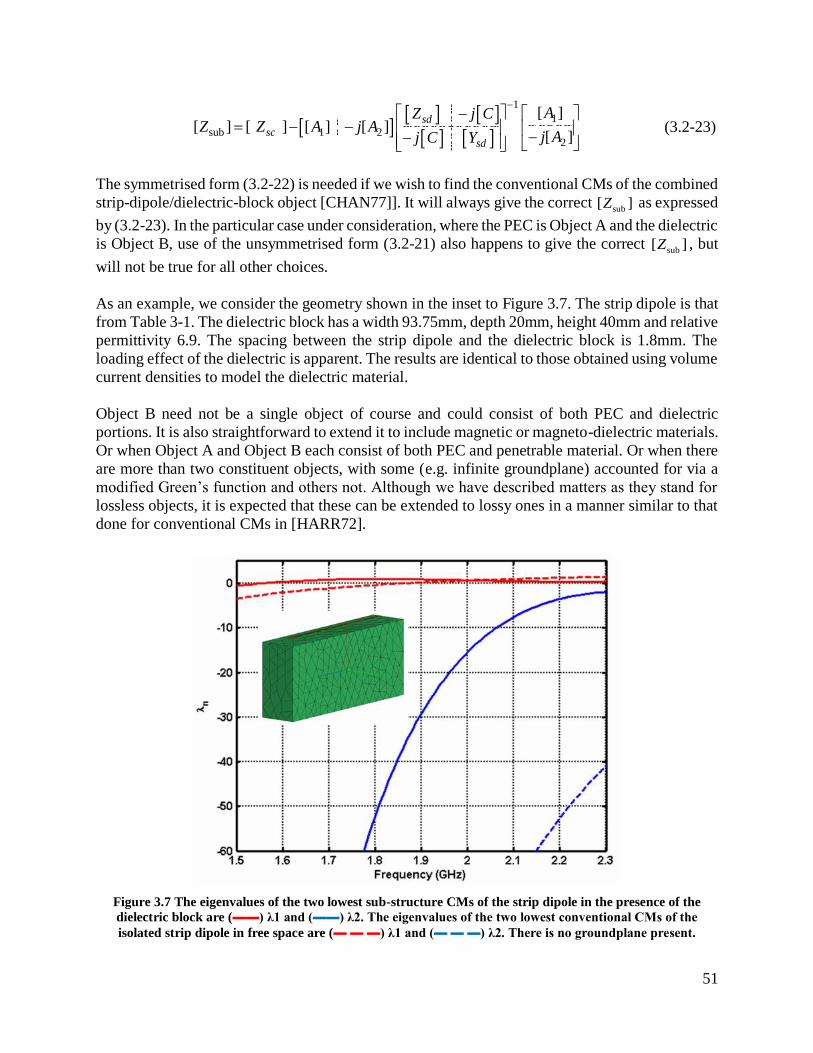
51
1
1
sub 1 22
[ ][ ] [ ] [ ] [ ]
[ ]
sd
scsd
AZ j CZ Z A j A
j Aj C Y
− −
= − − −−
(3.2-23)
The symmetrised form (3.2-22) is needed if we wish to find the conventional CMs of the combined
strip-dipole/dielectric-block object [CHAN77]]. It will always give the correct sub[ ]Z as expressed
by (3.2-23). In the particular case under consideration, where the PEC is Object A and the dielectric
is Object B, use of the unsymmetrised form (3.2-21) also happens to give the correct sub[ ]Z , but
will not be true for all other choices.
As an example, we consider the geometry shown in the inset to Figure 3.7. The strip dipole is that
from Table 3-1. The dielectric block has a width 93.75mm, depth 20mm, height 40mm and relative
permittivity 6.9. The spacing between the strip dipole and the dielectric block is 1.8mm. The
loading effect of the dielectric is apparent. The results are identical to those obtained using volume
current densities to model the dielectric material.
Object B need not be a single object of course and could consist of both PEC and dielectric
portions. It is also straightforward to extend it to include magnetic or magneto-dielectric materials.
Or when Object A and Object B each consist of both PEC and penetrable material. Or when there
are more than two constituent objects, with some (e.g. infinite groundplane) accounted for via a
modified Green’s function and others not. Although we have described matters as they stand for
lossless objects, it is expected that these can be extended to lossy ones in a manner similar to that
done for conventional CMs in [HARR72].
Figure 3.7 The eigenvalues of the two lowest sub-structure CMs of the strip dipole in the presence of the
dielectric block are (▬▬) λ1 and (▬▬) λ2. The eigenvalues of the two lowest conventional CMs of the
isolated strip dipole in free space are (▬ ▬ ▬) λ1 and (▬ ▬ ▬) λ2. There is no groundplane present.

52
Sub-Structure Modes – Orthogonality Properties
The orthogonality properties of sub-structure CMs are not all obvious. We have given rigorous
proofs of these for the first time. The mathematical details have been relegated to APPENDIX C.
The properties are listed directly below.
Property#1
[ ] [Z ][ ] (1 )Asub H Asub sub
m sub n n mnJ J j = + (3.2-24)
As with conventional CMs, arbitrary surface currents on Object A (in the presence of Object B)
can be expanded in terms of sub-structure CM currents of Object A, allowing one to perform this
expansion without needing to expand the currents on the secondary Object B.
Property#2
Bsec Bsec
[ ] [ ][Z ] (1 )
[ ] [ ]
HAsub Asub
fs subm n
n mn
m n
J Jj
J J
= +
(3.2-25)
The combined currents on Object A and Object B satisfy the orthogonality properties; in other
words, the current on Object B does not break the properties expected of CMs.
Property#3
Bsec Bsec
[ ] [ ][ ]
[ ] [ ]
HAsub Asub
fsm n
mn
m n
J JR
J J
=
(3.2-26)
Comparison of the results (A.C-1)19 and (A.C-17) shows that the current on Object B does not
contribute to the radiated power - it just redistributes it. This is to be expected since the CM current
on the Object A is the only “source”. The currents on Object B are not new sources of power. They
are just secondary to Asub
nJ which “already knows” about secB
nJ . The cancelling effect of the terms
in (A.C-8) occurs because the power coupled to the object B is negative, but then re-radiates and
becomes positive again and we have the power balance. In other words, whatever power Object B
sinks from Object A will inevitably be re-radiated because Object B is a PEC structure (and hence
does not dissipate power).
Property#4
Bsec Bsec
[ ] [ ][X ]
[ ] [ ]
HAsub Asub
fs subm n
n mn
m n
J J
J J
=
(3.2-27)
19 (A.C-#) is an expression listed in APPENDIX C

53
Property#5
The far-zone fields of the sub-structure CMs are orthogonal over the sphere at infinity, and so
satisfy a relation identical to (3.2-8)
The Ubiquitous Conducting Groundplane
Recall that we mentioned in Section 2.5.4, and then again more recently in Section 3.2.5, that
in all DRA antennas used in practice, the DRA is located on a conducting planar groundplane.
Thus, when we compute the CMs of the DRA we will assume a groundplane that is infinite in
extent and find the CMs using an IE that has the appropriate modified Green’s function in its
kernel. In other words, we will always compute modified20 (or equivalently sub-structure) CMs of
the DRA. Before doing this, it is worthwhile to pause for a moment to ponder the relationship
between the conventional CMs of a DRA, and its modified CMs with an infinite groundplane
present.
Consider therefore the “isolated” (no groundplane) notched DRA from Section 3.2.2, shown here
in Figure 3.8 (a). Its conventional CM eigenvalues are the solid curves in Figure 3.8. The
coincident solid red and black curves represent two CMs that are degenerate because of
geometrical symmetry about the xy-plane. The solid green and brown curves are CMs that are not
degenerate. We will call these results the original CMs.
We next slice this object in half and place it on an infinite PEC groundplane, in the two different
ways shown in Figure 3.8 (b) and (c). Notice that in Figure 3.8 (b) the dimension 8.77x8.77x3.61
(all in millimeters) from (a) has been halved, whereas in Figure 3.8 (c) dimension 8 has been
halved. Image theory (in the groundplane) allows one to replace the groundplane by an appropriate
image of the actual electric polarization current densities in the dielectric object. Horizontal
components of the polarization current would have out-of-phase images, whereas vertical
components of the polarization current have in-phase image currents. Thus, the set of CMs for the
geometries in Figure 3.8 (b) and (c) should be similar to those of the isolated DRA shown in Figure
3.8 (a), except that some modes present in (a) would be forbidden in (b) or (c) due to the imaging
effect only allowing the even or odd polarization current restrictions mentioned. In general, details
will depend on the polarization current distributions of the modes and the shape of the DRA, but
the arguments given are always borne out by computational results. Figure 3.9 illustrates this for
the geometries of Figure 3.8 (b) and (c). In the case of geometry (b) there is only one of the original
CMs (the green-circles curve) still present. For geometry (c) there are three of the original CMs
still possible (shown as the crossed blue, red and brown curves), but no degeneracies. All cases
were modelled using the code FEKO
20 It was shown analytically that the substructure CMs of finite-sized objects are the same as the modified CMs in
which the MoM solution matrix is based on a known modified Green’s function [ALRO13]. This is a very important
observation since the solution for the modified CMs provides us with the set of CMs that allowed for an object in
vicinity of an infinite ground plane.

54
(a)
(b) (c)
Figure 3.8: Calculating conventional CMs in (a) of an isolated DR compared to calculating the modified CMs
in (b) and (c) in which the presence of an infinite PEC ground plane is accounted for by a modified Green’s
function. The difference between (b) and (c) is the particular way in which the DRA has been sliced in half.
Figure 3.9: CM eigenvalues corresponding to the geometries shown in Figure 3.8. The solid lines are for
geometry (a), the circled-lines for (b), and the crossed-lines for (c). Color variation signifies different modes.

55
Controversies Regarding the CMs of Dielectric Objects
The cause of these non-physical modes mentioned in Section 3.2.2 was conjectured by
[MIER17] to be the non-uniqueness problem referred to in Section 2.4.5, but this has been disputed
[LIAN17].
There is a second subject of disagreement in the prevailing literature. In the case of the CMs of
PEC objects, it is universally agreed that the eigenvalue of the n-th CM can be interpreted as being
the ratio of the reactive power to the radiated power of the n-th CM. In the case of dielectric objects
one group of protagonists (e.g. [LIAN17]) claims to have shown that the same eigenvalue
interpretation is applicable to lossless dielectric objects. The other group (e.g. [MIER17])
maintains that this is not so. Both sides, however, agree that the frequency at which the n-th mode’s
eigenvalue becomes zero is a resonance in the sense that the reactive power of the n-th mode is
zero. The disagreement is the interpretation at off-resonance frequencies.
Thirdly, in some earlier papers (e.g. [CHEN14], and [CHEN15]) on the use of CMs in the analysis
of DRAs it was stated that the resonance frequencies of the CMs of these objects were one and the
same as the NM frequencies. This has been disputed in [BERN18]. The latter references classify
the natural modes into internal and external ones, depending on their behavior as the relative
dielectric constant goes to infinity. We prefer the classification terminology used in the 1970’s by
Van Bladel [BLAD07] who called these interior and exterior natural modes. Both kinds are natural
modes. At any rate, [BERN18] show for the two-dimensional case (an infinite dielectric cylinder
of circular cross-section) that the NM frequencies are in general not exactly equal to the CM
resonance frequencies but are only approximately equal for large relative permittivity values.
At the time writing of the present thesis these “disagreements in the literature” have been
recognized21 but the issues remain unresolved. Fortunately, uncertainties as to the cause of the
non-physical CMs do not hinder the actual computation of the CMs of dielectric objects using the
SIE because of the author’s contribution [ALRO14]. Also, we will in this thesis not rely on a
particular interpretation of the eigenvalues at frequencies off resonance, as will be explained in
later sections. Finally, we do not work with the NMs at all, and so the nearness (or otherwise) of
natural mode frequencies to CM resonance frequencies is not of concern.
CHARACTERISTIC MODES VERSUS NATURAL MODES
Why use characteristic modes (CMs) rather than natural modes (NMs)? This question has
been asked of the author in conference presentations and elsewhere. The reasons can be bulleted:
■ Computationally, the CMs are easier to compute than NMs when applied to the type of problem
of interest (namely an open dielectric resonator). The CM calculation involves linear eigenvalue
problems, whereas the NM determination uses non-linear eigenvalue problems. The latter are
computationally very taxing, as is clear from [KAJF83]. In the DRA antenna shaping process
21 As recently as the meeting of the Special Interest Group on Characteristic Modes at the 12th European Conference
on Antennas and Propagation (EuCAP 2018) in London, United Kingdom, in April 2018.

56
described in Chapters 4 and 5 the NMs of literally hundreds of candidate shapes would need to be
found. This would be prohibitive. CMs are the preferred route.
■ As stated in Section 2.3, natural modes are those that exist without the presence of an impressed
source, but each only at a different discrete frequency. The characteristic modes are available at
all frequencies.
■ The fields of the CMs are, in the terminology of rigorous electromagnetic formulations, the
scattered fields only. Once an impressed source has been specified, its fields in the absence of the
scatterer (DRA in our case), which are the incident fields incE and
incH of the problem, are known.
This is used to find the modal weighting coefficients n . The scattered far-zone field is then given
by the summation ( )1
,n n
n
E
=
. In proper DRA design it is the latter field that dominates the
radiation pattern of the DRA antenna, due to the strong coupling between the impressed source
and the desired CMs (that is, large values of the modal weighting coefficients n ).
■ The orthogonality properties of the CMs mentioned in Section 2.5.2 are often highly desirable
in the shape synthesis of certain DRA antenna types, as will be demonstrated in Chapter 5.
THE CONVENTIONAL RECTANGULAR DRA: DEFORMATION &
SCALING
Map of the Systematic Examination of the CMs of Conventional DRAs
The review in Section 2.5.5 concluded that relatively scant use has been made of CM analysis
of DRA antennas. There are only a limited number of existing references on the subject. The goal
of this section is to perform a more systematic CM analysis of DRAs to confirm some “common-
sense” expectations using a CM viewpoint. This will inform us on the way to approach the whole
DRA shape synthesis process to be built up in Chapters 4 and 5.
As a reminder on mode numbering, we note that the CM with the lowest first resonance frequency
is usually labelled as 1, that with the next highest resonance frequency as 2, and so on upwards. If
a mode does not go through resonance within the frequency range of a calculation, then an index
number is to be assigned based on ascending eigenvalue magnitude with the letter ‘n’ in front of
the index number. However, in some cases in Chapter 5, where the shape synthesis purposefully
results in certain CMs not being excited, even though they may not be insignificant, this was of
numbering CMs makes little sense. The actual numbering used will be made clear in the discussion
in such situations.

57
Computational Electromagnetics Code Verification
It is a truism that inaccurate results, albeit rapidly computed, is of little use. In all the results
to be presented the mesh density (and hence the number of expansion functions used to represent
the unknown quantities in the IE/MM analyses) is such that a converged result is obtained. This is
done on a problem-by-problem basis. This being understood, no further comment is necessary.
Square & Rectangular DRAs
This section shows how degenerate CMs can be obtained or removed and how a change in
DRA dimensions can play a role in affecting the CMs. A general rectangular DRA geometry is
shown in Figure 3.10. In this case, the height is doubled since the DRA is isolated (no infinite
ground plane). The first four eigenvalues of the special case of a square ( w d= ) DRA are plotted
versus Figure 3.11. Two of the modes (namely n2 and n3) are clearly degenerate modes (i.e.
identical eigenvalues) and hence have the same resonant frequencies. Such degeneracies are due
to the DRA having w d= . The lowest order CM is referred to the mode that goes through
resonance first ( 1 0 = at 5.65 GHz) and the second order CM is the referred to the mode that goes
through resonance second. The near and far-fields for the lowest and second order mode are
respectively depicted in Figure 3.13 and Figure 3.14, and by looking at both electric and magnetic
field distributions, both modes have like an electric dipole fields except that one is horizontal and
the other is vertical.
Making the dimension in x a little bit larger would void the symmetry in x-y plane, so we changed
it from 8.77 mm to 13.155 mm (100% increase). Clearly in Figure 3.12, the degenerate modes
(mode 2 and 3 in solid red and dashed black) for the original geometry presented in Figure 3.11
are no longer degenerate (mode 2 and 3 in solid red and black). The geometry was made larger so
naturally, we expect the modes to shift to lower frequencies.
Figure 3.10 Rectangular DRA (the square DRA being a special case). the dimensions are 8.77w d mm= = ,
3.51h mm= , and dielectric constant is 37.84r = .

58
Figure 3.11: Eigenvalues of the first four CMs of a square DR.
Figure 3.12: Eigenvalues of the first four CMs of a “non-square” DRA compared to those of the square DRA
also shown in Figure 3.11.The non-square DRA.

59
(a)
(b)
(c)
Figure 3.13: a). Electric field magnitude, (b). Magnetic field magnitude, and (c). Far-zone field, plots of the
lowest order CM of the square DRA at its resonance frequency of 5.65

60
(a)
(b)
(c)
Figure 3.14: (a). Electric field magnitude, (b). Magnetic field magnitude, and (c). Far-zone field, plots of the
2nd order CM of the square DRA at its resonance frequency of 7.56 GHz.

61
Dimensional Scaling of DRAs
In this section, it is shown that scaling all DRA dimensions of DRAs results in a linear
frequency shift for CMs, inversely proportional to a scaling factor. Basically, if the dimensions are
scaled by a factor x, the frequencies are shifted by 1( )x− . This is expected from theorem of
similitude [SINC 48], [POPO 81]. For example, doubling all the dimensions (x=2) of the square
DRA shown in Section 3.4.3 and keeping the dielectric constant fixed should yield to halving the
resonant frequencies of the individual mode with their associated magnitude too. Figure 3.15
shows a plot22 of the eigenvalues for the lowest 4 modes for both cases in which the eigenvalues
are the same for both cases when the frequency of the double dimensions is half now. This holds
true for the field distributions, radiation patterns, and MWC for any scaling factor.
Figure 3.15: Eigenvalues of the first four CMs of the original square DRA also shown in Figure 3.11 (solid
lines) compared to the double scaled square DRA (dashed lines). All the eigenvalues are represented with the
same colour in this plot, the degenerate mode’s curves are laying on top of each other’s.
Material Scaling of the Square DRA
It might be thought that a shift in the CM eigenvalues versus frequency curves can also be
achieved by scaling the dielectric constant r of the DRA material, with the scale factor being
old new
r r . However, a more careful reading of the theorem of similitude exposes the fact that
22 The double y axis plot is used to show the two different ranges of frequencies due to scaling.

62
such scaling would be possible if the dielectric constants of all materials in which the fields exist
are scaled. This means that the properties of both the DRA and the surrounding space must be
altered to obtain a simple shift of the eigenvalues curves along the frequency axis. This is obviously
not a scaling operation that is of any practical interest.
As an example of material scaling, the dielectric constant of the square DRA was increased from
37.84 to 50 ( 37.84 50old new
r rto = = ), and a comparison between the eigenvalues of the original
square DRA discussed earlier and the square DRA with the higher dielectric constant is shown in
Figure 3.16. The right-hand side vertical axis are the frequencies at which the eigenvalues of the
square DRA with the higher dielectric constant were calculated, and the frequencies were
determined based on the factor of old new
r r . The two curves corresponding to the two cases are
not aligned, meaning that the material scaling is done by that simple factor due to the fact that the
surrounding medium was free space for both cases.
Figure 3.16: Eigenvalues of the first four CMs of the original square DRA also shown in Figure 3.11 (solid
lines) compared to the same square DRA new
r increased to 50 (dashed lines). All the eigenvalues are
represented with the same colour in this plot, the degenerate mode’s curves are laying on top of each other’s.
Circular DRA
Unlike the square DRA, sets of degenerate CMs are always expected for any circular DRA (a
disk or puck) due to the rotational symmetry in the geometry, and since voiding symmetry is not
63
possible with a disk, then degenerate CMs shall always accompanied with such geometry.
Nevertheless, CMs of a circular DRA are not necessarily all degenerate sets. Voiding the symmetry
in the square DRA was possible by simply making all the dimensions different.
Square DRA with Notch
Placing a notch in a DRAs is one of the methods that have been used to try improve the
bandwidth, as discussed in Section 2.3.5. As an example to demonstrate what the notch impact on
the CMs, a notch was truncated from the square DRA presented in Section 3.4.3. The same
geometry was analyzed in [LIU01] in which MoM solution of the EFIE was used to determine the
dominant natural mode resonance, which is found to be around 6.125 GHz. The notch has a width
and depth of 2 mm, and it has the same height as the DRA. In Figure 3.17, the shape of geometry
along with the CM eigenvalues is shown, and by comparing theses eigenvalues to the ones shown
in Figure 3.11, the first observation is that the degenerate modes shown there (mode 2 solid and
dashed red) are slightly23 separating due to presence of the notch. The second observation is that
the dominant CMs resonates at 6.128 GHz, instead 5.65 GHz for the similar mode of the unnotched
DRA. Note that the CM resonance is approximately equal to the natural mode found in [LUI01].
Next, we examine the field distributions of the dominant mode shown in Figure 3.18 and compare
them to those corresponding to the unnotched shown in Figure 3.13. Since the truncated notch was
in the intensity path of the horizontal components of electric fields, the CM eigenvalue was
affected and shifted to higher frequency, and the lower effective permittivity24 causes the fields to
concentrate in the air region.
What if the same notch is truncated from the center of the square DRA?. Since E is relatively
small in the central region of the DRA for the dominant mode, as observed in Figure 3.13, the
associated eigenvalue and resonance were not affected by such a centrally located notch, unlike
the above-mentioned boundary notch. In Figure 3.20, the corresponding field distributions are
shown, and one can observe there is a negligible change in the distribution compared to the original
square DRA, which does not have a notch. Therefore, it is imperative that the modal field
distributions are studied to understand the impact of shaping DRAs on them. The classical
perturbation theory [STAE 94] of closed resonant cavities with PEC walls shows that changes in
the permittivity at locations where the original electric field strength of a natural mode is small has
a much smaller influence on the natural mode’s frequency than changes where its electric field is
large. Although the DRAs we are dealing with here are open resonators, their natural mode
frequencies (when they are of rectangular or hockey-puck shape) have been determined
approximately by assuming them to be surrounded by walls of perfect magnetic conductor (PMC).
Perturbation theory could be worked out for such approximate models of DRAs, and hence the
behavior observed above is not unexpected. Quantitative expressions obtained from perturbation
23 Unlike the curves related to the degenerate modes Figure 3.11, the two curves are not sitting on top of each others. 24 The effective permittivity is considered lower since air was introduced in the region in which the intensity of electric
field was high.

64
theory for resonance shifts only apply for small changes (implied by the use of the term
“perturbation”), it being assumed that the change is so small that the field distribution of a mode
alters negligibly when the change is made. If we wanted to determine the effect of another small
change we would have to find the fields of the actual altered modal fields and then re-apply the
perturbation formula for a new estimate of the resonance frequency, and so on. In the shape
synthesis process to be discussed in Chapter 4 and 5 the changes made from one shaping iteration
to another will be seen to be small25, and so in a way the process successively applies perturbations.
After several perturbations the DRA shape, and the modal field distributions, will be significantly
different from those of the DRA with which we began. Fortunately, the use of the CM approach,
stemming as it does from a rigorous computational electromagnetics solution, obviates the need
for perturbation theory.
The CM analysis of this section, and other computational results observed but not and the present
section, has provided a strong indication that when one removes dielectric material from a given
DRA shape, the CM resonance frequencies either remain much the same or increase. This
observation will also be borne out by the DRA shape synthesis examples that are the subject of
Chapter 5, although a rigorous proof that this must always be so has been found. It seems intuitive
though, in that removal of material suggests (albeit vaguely) a lowering of the effective
permittivity of the object.
25 Since we only adjust the electrically very small voxels into which the starting DRA is meshed. More will be said
on this topic in Chapter 4.

65
Figure 3.17: Eigenvalues of the first four CMs of the boundary notched square DR shown the top left.
Figure 3.18: a). Electric field magnitude, (a). and Magnetic field magnitude, and (b), plots of the lowest order
CM of the boundary notched square DRA at its resonance frequency of 6.128 GHz

66
Figure 3.19: Eigenvalues of the first four CMs of the centered notched square DR.
Figure 3.20: a). Electric field magnitude, (a). and Magnetic field magnitude, and (b), plots of the lowest order
CM of the boundary centered notched square DRA at its resonance frequency of 6.58 GHz

67
3.5 CONCLUDING REMARKS
Characteristic mode concepts are central to the shape synthesis procedure for DRA antennas
that is developed in this dissertation. A fresh look at some basic aspects of the topic was therefore
given in Section 3.2. More robust methods for tracking the modes of dielectric objects were
described. Although not yet used in commercial software packages, in those instances where the
latter fail to properly track CMs over frequency we are able to use these new tracking methods
“manually”. Thus, all results in the dissertation are properly tracked. The sub-structure CM
concept was broadened; certain assumptions previously thought necessary were shown to be not
so. The CMs computed using Green’s functions other than the free space ones were shown to be
equivalent to sub-structure modes. The broadened numerically determines sub-structure CMs are
more general in practice, however, since they do not actually require knowledge of complicated
modified Green’s functions (of which few are known). Tis clarified the fact that the CMs to be
computed in Chapters 4 and 5, of DRA objects on infinite conducting groundplanes are in fact sub-
structure CMs. The sub-structure CM ideas were then extended to include composite object,
composed of conductors and dielectrics. Formal mathematical proofs of the orthogonality
properties of sub-structure CMs were provided for the first time. Controversies that still exist in
the literature in the interpretation of the CMs of dielectric objects have been identified and
discussed; we explained why the way CMs are used in this work are unaffected by these
disagreements between researchers. Apart from being important to the work of this dissertation,
the studies in Section 3.2 also add to the advancement of CM theory generally. Most of this s basic
work has already been described in the following publications:
H.Alroughani et al., “Sorting the characteristic modes of PEC objects not electrically small”, 12th European
Conference on Antennas and Propagation (EuCAP 2018), London, UK, April 2018.
H.Alroughani et al., “Clarifications on the surface integral equation computation of the characteristic modes of
dielectric objects”, IEEE AP-S Int. Symp. Digest, San Diego, USA, July 2017.
H.Alroughani, "An enhanced algorithm in tracking characteristic modes of dielectric objects", Applied
Computational Electromagnetics Symp., Florence, Italy, April 2017.
H.Alroughani et al., “On the orthogonality properties of sub-structure characteristic modes”, Microwave & Optical
Technology Letters, Vol.58, No.2, pp.481-486, Feb.2016.
H.Alroughani et al., “Numerical experiments in tracking the characteristic modes of dielectric objects”, 2016
IEEE/ACES International Conference on Wireless Information Technology and Systems (ICWITS) and Applied
Computational Electromagnetics (ACES) Symp. Digest, Honolulu, Hawaii, USA, March 2016.
H.Alroughani, "Studying microstrip patch antennas using the theory of characteristic modes", IEEE AP-S Int. Symp.
Digest, Vancouver, Canada, pp. 1476-1477, July 2015.
H.Alroughani et al., “On the classification of characteristic modes, and the extension of sub-structure modes to
include penetrable material”, Proc. ICEAA '14 / IEEE APWC '14 Symp., Aruba, August 2014. (CD-ROM).
Some of this has already been used in the work of others (e.g. [BERN 15]). Section 3.3 related
characteristic modes (CMs) to natural modes (NMs). This was important because most engineers
are more familiar with NMs than CMs. The difference is easy to grasp but is often not explicitly
stated. It was necessary to do so here so that we could appreciate why CMs are a refreshingly
computationally efficient alternative to NMs and serve all the same purposes for present
applications. Finally, Section 3.4 examined the CMs of various conventionally-shaped DRAs.
Although some authors had used the CM approach to estimate the natural frequencies of DRAs of
conventional shape little else had been done. Thus Section 3.4 acquainted us with a CM exposure
of some “I knew that” electromagnetics principles. The groundwork has been laid for confidently
using CMs with understanding in the chapters that follow.

68
CHAPTER 4: DIELECTRIC RESONATOR ANTENNA
SHAPE SYNTHESIS TOOLS
PRELIMINARY REMARKS
It will be noticed below that the objective functions are not simple mathematical functions but
contain searching and decision making in their definitions as well. The reader might then wonder
why the GA is used at all. Would not a simple direct search do the job? However, we know from
courses on digital systems that the number of ways the bits in a binary word of length n can be
arranged is 2n . If n is on the order of 50, then there will be more than 1,125,899,906,842,624
arrangements to examine. This prohibits a direct search, since a full-wave electromagnetic
simulation would be required for each arrangement examined. The GA’s evolutionary approach
drastically reduces the number of actual arrangements that actually need to be examined.
The implementation of shape synthesis of dielectric resonator antennas can take various forms;
however, the scope of this dissertation is narrowed down to three possible different approaches:
using VIE-based MoM, VIE-based MoM BOR, and SIE-based solution. The latter approach is
decided to be the most feasible one due to computational efficiency, simple implementation,
compatibility with arbitrary shapes and robustness, and hence it was used in the optimization
process which is deliberated throughout this chapter and following one. Still, the earlier two
approaches will be discussed in the subsequent sections to shed the light on their incompatibility.
Before the chapter is concluded, some cases of study are then presented to illustrate the use of CM
analysis in studying DRAs, especially by calculating the modal weight coefficients (MWCs) and
having a valid interpretation which assist us in forming some of the objective functions discussed
in the next chapter.
THE SHAPE SYNTHESIS TECHNIQUES
Shaping Technique using VIE-based MoM Approach
The form of segmentation that takes place in the solution of VIE-based MoM is tetrahedral
elements which is modeled with a volumetric current density and the expansion functions are
placed on those elements. Therefore, the removal of such tetrahedrons can actually shape the
geometry under such analysis; the beauty of doing such thing is that the MoM-solution matrix can
be reconstructed with a simple elimination of rows and columns corresponding to the expansion
function of the removed tetrahedron. For an accurate VIE-based MoM solution, the required
number of unknowns (i.e. expansion functions) is usually significantly large compared to FEM or
SIE-based MoM, for example; as a result, the computational time for both MoM solution and CM
analysis can be very expensive, especially if used in a optimization process in which many
iterations are needed. The preliminary proposal was to use this approach due to the fact it offers
the simplicity in shaping using the MoM segmentation and the CM analysis provides only physical

69
modes unlike the SIE-based approach. The implementation of this approach was done using an
interface between FEKO and MATLAB. In FEKO, a MoM solution is performed on the unshaped
geometry (e.g. RDRA), and then the data such as the solution matrix, and information on the
element’s positions and expansion functions are all exported to MATLAB environment. The step
of performing MoM solution in FEKO is only required once since they matrix can be reconstructed
for every shaping iteration in MATLAB environment in which CM analysis and optimization can
be done. The in-house code written in MATLAB allows the ease of importing all the necessary
data from FEKO and connects dots when it comes to the removal of solution tetrahedrons and their
corresponding matrix elements. In Figure 4.1, the final shaped isolated DRA (using symmetry
along the height) was achieved using a simple function to shift the resonant frequency of the
dominant mode. Although it was a successful implementation, we had come to a realization that
the final shaped for even a simple objective function can be tricky even with additive
manufacturing technology due to the limited achievable resolution. The tetrahedrons can be very
tiny and may not cope with the resolution of 3-D printers available to us. In addition, we found out
even with a coarse mesh that solving eigenvalue equations for every iteration can take tremendous
amount of time. Therefore, it was concluded that other options must be explored.
Figure 4.1: shaped DRA using VIE-based approach by removing tetrahedrons.
Shaping Technique using BOR-based MoM Approach
Another approach that was considered is the solving of the IEs using the body-of-revolution
(BOR) MoM approach which is applied to rotationally symmetric geometries such as the geometry
shown in Figure 4.2. The solution of BOR is based on harmonic-by-harmonic scheme [KUCH00a],
and it can be either based on SIE or VIE. But then again, the VIE solution was considered since
only physical modes are desired as the output of the CM analysis to which BOR formulation can
be applied. The application of CM analysis using VIE-based BOR formulation has not been
attempted yet; however, we see no reason why it cannot be a valid analysis as it was attempted for
SIE-based BOR in [ALRO13]. Unlike the 3-D VIE-based MoM solution, which uses RWG basis

70
functions, discussed in the preceding section, the number of unknowns required for the BOR
solution is significantly reduced due to the fact on a surface layer of the intended geometry is
meshed with triangular elements as shown in Figure 4.2. Thus, computational resources is not an
issue here; however, the approach is only limited to rotationally symmetric geometries which
might not be necessarily something of interest, especially when the widely-used cubical or
rectangular DRA are studied. For reasons mentioned, it is evident that abandoning both the
approach presented in this section, and that in Section 4.2.1, was reasonable after we came to a
conclusion that the third approach, discussed in Section 4.2.3 that follows, is the most feasible.
Figure 4.2: the BOR approach applied to rotationally symmetric geometries [KUCH00a].
Shaping Technique using SIE-based MoM Approach
The surface integral equation (SIE) offers the same MoM solution as the case with VIE by
instead solving fictious electric or/and magnetic current densities along the object’s surface,
whereas it is the real polarization currents in the object’s volume using VIE formulation. Hence,
an expansion functions (i.e. RWG basis) are placed on the edges of triangular elements in SIE
solution as opposed to the edges of tetrahedral elements in VIE solution. The SIE approach is more
ideal than the VIE approach since the computational time and memory allocation are more
practical and efficient since the size of the MoM matrix of SIE solution is drastically smaller
compared to VIE-based MoM solution. For instance, to have sense of the difference in number,
the number of knowns for fine meshing for a problem using SIE and VIE is 720 to 6752 unknowns,
respectively. Now, one can clearly see why VIE solution is avoided. This is the beauty of the SIE
solution – a rapid computation time. Having said that, unlike the VIE solution, the CM analysis
suffers from the non-physical modes when a PMCHWT26 formulation is used in the application of
26 PMCHWT formulation is used in CM analysis and was discussed in Section 2.4.5.

71
the CM analysis. Such dilemma can be easily solved by using the method proposed in [ALRO14],
so after a CM analysis is performed, there is that one extra step need - which is filtering out those
non-physical modes by examining the far-field orthogonality. The other downside of using the
approach discussed here is that the MoM matrix must be recalculated to perform CM analysis
during the shaping process, unlike the case with VIE-based approach in which the mesh used in
shaping. Here, the intention is to break the starting geometry (e.g. rectangular dielectric box) to
blocks (voxels) which are not part of the solution mesh, so the surface of the shaped geometry with
those voxels must be meshed again. Although there are two extra steps are needed for SIE-based
approach compared to the VIE-based approach, the computational time is still way more efficient.
In addition, one has the freedom to decide the size and shape of the blocks which is a separate
entity from the MoM solution and hence meshing. Hence, it has been concluded that the SIE-based
approach is the way to go. In Section 4.3, a further elaboration on what type of voxels are used
and how it is done.
GEOMETRY & MATERIAL CONTROL
For reasons mentioned in Section 4.2, the SIE-based approach is to be employed in the shape
synthesis of dielectric objects through analyzing their CMs, so breaking the starting geometry to
small blocks is proposed. Throughout this dissertation, voxelization is strictly applied to shapes
that can be easily divided, and such shapes are simply RDRAs (or rectangular dielectric boxes)
due to their popularity and the degree of freedoms that they offer. Still, the same concept can be
applied to any arbitrary shape. The shape of such voxels (blocks) is chosen to be cubic or
rectangular because of its simple implementation, especially with RDRAs, but in general, the
shape of the block may take any form. A MATLAB function “CubeVoxels” is used by specifying
the dimensions (w x d x h) of a starting object, in x, y, and z directions. The block whose
dimensions are determined based on the entire size of the starting geometry and the number of
blocks in x, y, and z directions is uniform in size with a homogenous dielectric material. As a
demonstration of voxelization in Figure 4.3 (a), a cube with 3-mm sides is divided into 3 blocks in
x, y and z, so it is composed of 27 cubic blocks of 1 mm3 in volume.
A fitness function created in MALAB is executed using GA optimization in which the voxelated
shape is assigned to a chromosome string: when the bit is “1” the voxel is present otherwise it is
not. For the example shown in Figure 4.3 (a), the associated chromosome of the that shape must
then be represented by 27 bits, and since all the blocks are present in this case, then the entire
chromosome string is made of ones. The fitness function contains the objective, which is specified
by the user; examples of some objective functions are discussed in Chapter 5. The inputs to the
fitness function are the random chromosome generated by the GA and parameters which include
information on the geometry shape, dielectric material, frequency of operation, mesh size, number
of CM desired to be computed, and a directory in which the file (DXF extension type) containing
the coordinates of the voxels for the shaped geometry is saved. For each individual, the shaped
geometry formed through a chromosome is then exported to FEKO; this step is performed through
running Lua script editor27 from MATLAB. The script makes the automation process possible for
creating a FEKO model that involves the following: unionizing and simplifying the imported
27 A programming language embedded in FEKO interface that easy to write.

72
shaped geometry, assigning the unionized geometry to a lossless dielectric material with the
specified dielectric constant, placing the geometry on infinite ground plane (i.e. not isolated
dielectric), specifying frequencies, meshing the geometry, requesting near- and far-fields, and
finally computing CMs. It is worth mentioning that the number of CMs calculated in FEKO can
be specified, and it is recommend choosing a number between 100 to 150 modes since the total
number may include non-physical CMs which are routinely filtered out by FEKO, just as described
in [ALRO14]. Therefore, the user would only obtain the physical modes whose numbers might be
much fewer than the specified number of CMs.
A MATLAB function is then called from the fitness function to import the simulation data from
FEKO and to be processed based on the optimization goals. A considerable amount of time is spent
on waiting for the simulation completion and data import, whereas the rest of the optimization
process is relatively not as time consuming. FEKO simulation run time depends on the number of
frequency points, mesh size, requested field points, and number of CMs. Therefore, within the
fitness function, there are commands to only create a FEKO model for unique shapes (or
chromosomes); otherwise, the fitness value is assigned from a saved data based for chromosomes
for which their fitness value is already evaluated. Such steps save an enormous amount of time for
performing the same calculation since repeated chromosomes can appear at next generations such
as the elites. In addition, the fitness value for those chromosome strings containing more zeros
than ones is simply assigned to a high value if minimization is taking place; the fitness function
prevents creating a FEKO model for shapes that are electrically small or made of dispersed blocks
such as the case shown in Figure 4.3 (b). Another situation for minimizing the computational time
is to avoid running unnecessary FEKO models for the exact same geometry which made by two
different chromosomes; this may happen when there is a geometrical symmetry in the in x and/or
y axes only (not along z axis) since the infinite ground place is always placed at z= 0. This can be
demonstrated by the shapes and their corresponding chromosomes shown in Figure 4.3 (c) and (d):
the shapes are the indeed same when one of them is rotated, but the chromosome strings are
different.
A homogenous dielectric geometry is considered throughout this work, meaning that the individual
blocks used in shaping are tentatively filled with the same dielectric material. In FEKO, the
individual blocks are first unionized forming one or multiple regions to which the desired dielectric
medium is assigned to. Even though it is outside the scope of this dissertation, the individual blocks
can be actually filled with different dielectric or even conducting materials. Technically, the
surface formulation using the surface equivalence theorem in FEKO allows the computation of
such problem, and practically speaking, this is can be done with some high-tech 3-D printers that
can be available to the user. And by varying the material of the blocks, we can expand geometry
control to a material control, as well.

73
[111111111111111111111111111] [101011111001001100001000100]
(a) (b)
[111111111111111111001111111] [111111111111111111001111100]
(c) (d)
Figure 4.3: A demonstration of voxelization in (a), symmetry in (b) and (c), and dispersed shape in (d). The
chromosome associated with each shape is indicated below each.
COMMENTS ON OBJECTIVE FUNCTION CONSTRUCTION
In order to use optimization algorithms for the shape synthesis of DRA antennas (or indeed
any design purpose whatsoever) it is necessary to translate the design goals into a quantity that,
when minimized, provides an antenna that has the performance we desire. The most obvious way
to define an objective function in antenna work would be to use some well-chosen combination of
the input reflection coefficient 11S , the directivity, radiation efficiency, and so on, of the antenna28.
However, such quantities can only be found (during the shaping process) if the complete antenna
is modelled, as indicated in Figure 4.4. But we wish to shape synthesize DRA antennas without
having to completely specify the details of the physical feed mechanism, and its location, prior to
28 In multi-antenna systems (e.g. for MIMO usage) we would include the coupling terms ijS ( i j ) as well.

74
the shaping process. This reduces the constraints placed on the shape optimization process and
could lead to potentially new configurations due to the increased degree of freedom afforded.
We will show below how (using CM concepts) this can be achieved, with the feed location
determined as part of the shaping process, and only an idealized surrogate impressed source29
representing the chosen type of feed30 being used during shaping.
DDielectric
Resonator on
Infinite PEC
Plane
Specific Physical
Feed MechanisminZ
Computational
Electromagnetics
Model
Figure 4.4: Computational electromagnetics model of the antenna in all its detail.
The dielectric object that forms part of the complete DRA antenna is a porous resonator that
radiates electromagnetic energy into space. In order to utilize any resonator as an antenna we must
be able to strongly couple energy into and/or out of it through a port (that is formed by the physical
feed mechanism). If we do not want to commit to the feed mechanism details prior to shaping, how
can we perform a meaning electromagnetic analysis to guide the shaping process? This is where
the CM analysis come to our aid. Prior to shaping it will be necessary to at least decide on the
type of feed mechanism to be used. If it is a probe or proximity type, we will represent it by a
surrogate infinitesimal electric dipole. If it is a slot, we will represent it by a surrogate infinitesimal
magnetic dipole. This is depicted in Figure 4.5. We conjecture that if a desired31 CM (or CMs) has,
for the appropriately selected surrogate feed mechanism, a high modal weighting coefficient over
a frequency band of interest, which means that power is being strongly coupled to the particular
CM (or CMs), then this in turn means that in all likelihood it will be possible to “easily” detail an
actual physical feed mechanism of the type represented by the surrogate at the location of the
surrogate. This conjecture will be verified in two case studies immediately below.
Of course, with a physical probe (conducting material inserted), or physical slot (groundplane
material removed to form the slot), the CMs of the entire object will have changed slightly.
However, with strong coupling from the actual feed mechanism to the CMs of the DRA without
the physical feed, the examples studied all show that the said feed is not so intrusive that it
completely changes the radiation characteristics of the shaped DRA.
29 Infinitesimal electric or magnetic dipoles ˆ
ep or ˆmp , respectively. The expressions are listed in APPENDIX B.
30 Probe, proximity or slot, as outlined in Section 2.3.3. 31 Desired because, for example, it satisfies some radiation pattern demands (e.g. broadside; omni-directionality). We
do however recognise here that the single DRA antennas that we have in mind in this dissertation are not electrically
large, and so there is only a limited amount of radiation pattern control possible, as is also the case with single
conventional monopoles, dipoles, microstrip patches, and so on.

75
D
Dieletric
Resonator on
Infinite PEC
Plane
(No Physical
Feed Mechanism
Present)
Idealized
Impressed Source
Modal Weighting
Coefficients
( )n f
Computational
Electromagnetics
Model
Figure 4.5: Computational electromagnetics model of the DRA antenna used during the shape synthesis
process (and hence for CM analysis).
ILLUSTRATIVE CASE STUDY
In this section, two cases of study are examined to show the correlation between the MWC
and the return loss when DRAs are physically fed with a source such as a slot aperture or coaxial
probe and to show the potential of modal excitation. The first example is taken from the literature,
and the second example are based on a starting geometry for DRA shape synthesis discussed in
Section 5.3.1.
Probe Fed Square DRA
A rectangular DRA with a square cross section was designed and discussed in [ZOU16] to
operate effectively at dual bands with having omnidirectional radiation pattern. The dual bands are
the WiMAX and WLAN (3.5 and 5.8 GHz). The square DRA was fed in the center by a coaxial
probe and placed on the center of a ground plane of size 100 mm x 100 mm. The authors managed
to excite the higher order 121
xTE / 211
yTE and 141
xTE / 411
yTE 32 for bands 3.5 and 5.8 GHz, receptively.
The set of modes in each band is considered degenerate due to the square cross section (i.e.
symmetry); hence, both modes in the set should then resonate at the same frequency. The authors
also indicated that the excitation of such modes would result in the omnidirectional radiation
pattern which was desired in this type of work, achieved for the dual bands.
32 These are the natural modes of the RDRA. TE is an abbreviation for transverse electric.

76
Figure 4.6: The configuration (side and top views) of the square DRA in [ZOU16]. The design parameters
are: a = b = 38 mm, c = 10 mm, r = 9.8, l = 10 mm and gl =100 mm.
We have found some interest in such design since it is a simple conventional DRA with the two
design requirements, so these make the design suitable for a case study performed by the CM
analysis which will be used extensively in the next chapter. The CM analysis was performed for
the same square DRA placed on infinite PEC groundplane, and many significant CMs were
observed in the frequency range between 2.5 and 6.5 GHz in which dominant degenerate CMs are
found to resonate at 2.84 GHz. The modal field distribution of the dominant CM is like magnetic
dipole source, so it cannot be coupled by a vertical probe whose pattern is like an electric dipole
source. However, few higher CMs were found to have a radiation pattern that is omnidirectional
and can be coupled by a vertical probe (the surrogate). An infinitesimal electric dipole was placed
at the center of the DRA (0,0,5mm) to understand the design in [ZOU16] through the eye of CM
analysis. As depicted in Figure 4.7, the MWCs were calculated to examine into which mode the
power was coupled the most at various frequency points, and this can be eye balled by spotting the
peaks which occur at 3.40, 4.88, 5.58, and 6.44 GHz. The peaks also correspond to where their
corresponding eigenvalue goes through zero (i.e. resonance) except for that CM #1 whose
eigenvalue goes through zero at 3.28 GHz. Thus, it is not necessary that the MWC peak occurs at
the modal resonance. The MWCs then were found very informative as they have shown us that
only these four modes can be excited with the electric dipole source fed in the center at the
frequencies at the which the MWC is high and peaking. In addition, the peak width is indicative

77
of bandwidth as it will become evident when an actual coaxial probe is fed into the DRA. The
radiation patterns of the all the modes are omnidirectional as shown in Figure 4.8, and the electric
and magnetic fields within the DRA are shown in Figure 4.8 and Figure 4.9 are shown,
respectively, which they indicate that the field distribution of the modes are like an electric dipole
source.
Figure 4.7: The MWC of the square DRA due to the infinitesimal electric dipole source placed at the center.
CM #1 @ 3.44 GHz
CM #3 @ 5.54 GHz
CM #2 @ 4.88 GHz
CM #4 @ 6.44 GHz
Figure 4.8: The modal far fields for the corresponding to modes shown in Figure 4.7.

78
CM #1 @ 3.44 GHz
CM #3 @ 5.54 GHz
CM #2 @ 4.88 GHz
CM #4 @ 6.44 GHz
Figure 4.9: The modal electric fields corresponding to modes shown in Figure 4.7.
CM #1 @ 3.44 GHz
CM #3 @ 5.54 GHz
CM #2 @ 4.88 GHz
CM #4 @ 6.44 GHz
Figure 4.10: The modal magnetic fields corresponding to modes shown in Figure 4.7.

79
Next, the design in [ZOU16] was modeled in the commercial computational EM software package
[HFSS] except that the height of the centered coaxial probe was varied to examine the return loss
over the same range frequencies as done for the CM analysis, as shown in Figure 4.11 in which
the height was varied from 1 mm to 10 mm (DRA ceiling). One can clearly observe that a good
impedance matching, where the dip in return loss appears, can only be achieved around those
frequencies which coincide with the MWC peaks. This shows the potential of coupling the power
into only those DRA modes that permit to, and this can be seen through studying CMs and the
MWC. Also, one can notice that the MWC peak width becomes wider, the more potential the mode
has for a wider impedance bandwidth as it is manifested in the two peaks of 3.44 and 5.54 GHz
which correspond to the |S11| dips that can be widen (i.e. wider impedance bandwidth) around the
same frequencies, unlike the other two dips. On the other hand, when the value MWC is very low
for any mode at a frequency such as 5.1 GHz, the possibility of coupling the power into any mode
is slim, and a satisfactory return loss could not be attained even when the height was significantly
varied.
Figure 4.11: |S11| in dB for the square DRA fed with a center probe modeled in HFSS.

80
Probe Fed Unconventional Shaped DRA
Figure 4.12: The geometry of the studied unconventional shaped DRA.
This case study is inspired from the third examples on shaping discussed in Section 5.4, and
the geometry, shown in Figure 4.12, used to be a rectangular box of size 40 mm x 40 mm x 20 mm
divided into 75 blocks whose size is 8 x 8 x 6.67 mm. A manual shaping (no optimization involved)
took place by removing some of the blocks and resulted to the geometry as shown in the latter
figures. This was performed to study a case with a volume constraint requirement as it will be
discussed later in Section 5.4 in which the starting shape is slightly different, and the dielectric
material is different as well. As part of a shaping process, CM analysis is performed to observe the
modal fields in the near and far zone to locate the optimum position for feeding a DRA and identify
radiation pattern of individual modes. By examining the electric and magnetic fields in Figure 4.15
and Figure 4.16, the vertical component (perpendicular to the infinite ground plane) of the electric
fields is found to be strong in three different positions corresponding to CM #1, CM #2, and CM
#3; therefore, an electric dipole source can be considered since the field distribution around any of
these position is like an electric dipole source. A magnetic dipole source may also be used to excite
in CM #1 by placing it where the tangential components of the magnetic fields are strong along
with having the electric field circulating it. The radiation pattern of the individual modes is shown
in Figure 4.14, and if the most of the power is coupled into any of these modes once the DRA is
fed, then one should expect obtaining a similar pattern. However, multiple

81
Figure 4.13: The MWCs due to an infinitesimal electric dipole placed at three different positions. The curve
colors (blue, red, and black) indicate modes considered (CM #1, CM #2, and CM #3). The curve types (solid,
dashed, dotted dashed) indicate the source position (1,2, and 3).
CM #1 @ 2.05 GHZ
CM #2 @ 2.28 GHz
CM #3 @ 2.85 GHz
Figure 4.14: The modal far fields in 3-D for the corresponding modes shown in Figure 4.13.

82
CM #1 @ 2.05 GHZ
CM #2 @ 2.28 GHz
CM #3 @ 2.85 GHz
Figure 4.15: The modal electric fields in the DRA for the corresponding modes shown in Figure 4.13.
3
CM #1 @ 2.05 GHZ
CM #2 @ 2.28 GHz
CM #3 @ 2.85 GHZ
Figure 4.16: The modal magnetic fields in the DRA for the corresponding modes shown in Figure 4.13.

83
modes can possibly be excited at the same time, so the far field pattern results basically from the
superposition of the individual modes’ pattern. Let’s assume that one is tied to using a coaxial
probe, so in order to find out which mode most of the power is coupled into, an infinitesimal
electric dipole source is then to be used in the CM analysis to calculate the MWCs due to the
surrogate at three different positions, as listed in Table 4-1. The corresponding MWCs are depicted
in Figure 4.13. For a dipole source positioned at 1, 2, and 3 respectively, CM #1, CM #2, and CM
#3 were found to be strongly excited at 2.05, 2.28, and 2.85 GHz, respectively. Therefore, for this
specific shape, there are three different options with exciting three different modes at three
different frequencies; the broadside pattern can be obtained by either exciting CM #1 or CM #2
whereas CM #3 can provide an omnidirectional pattern. Note that some power can also couple into
mode CM #3 around 2.28 GHz by placing a probe in position #2 even though the majority of the
power was coupled into CM #2; hence, this might contribute to some radiation in the azimuth
plane (i.e. not purely broadside pattern). Another observation is that the MWC peak associated
with CM #3 are found to be the widest and highest, so one should expect a wider impedance
bandwidth can be achieved. Subsequently, this bring us up to simulating this DRA as a driven
problem in FEKO by solving for the S-parameters and the far fields of the probe-fed DRA. The
return loss at the probe is shown in Figure 4.17 for placing the coaxial probe in the same positions
using CM analysis. The height of the probe was adjusted to 10 mm when placed in position #2 or
#3 and to 12 mm for position #1 for a good impedance matching (i.e. a higher return loss). Just
like the previous case study, it is shown here that the return loss dips occur at a frequency roughly
around the frequency at which the MWC peaks, and feeding the DRA in position #3 which mainly
resulted in exciting CM #3 led to the broadest bandwidth, as indicated by the wider MWC peak.
Finally, the gain in two different cuts corresponding the three cases are shown in Figure 4.18
indicating that indeed exciting the DRA from position #1 and #2 provide the broadside radiation
pattern whereas position #3 provides the omnidirectional pattern.
Table 4-1: The different position where the infinitesimal electric dipole is placed for the unconventional DRA.
Position Number Dominant Mode Excited Position in (x , y , z) in mm
1 CM #1 (8,16,0.33) or (-16,-8,0.33)
2 CM #2 (-16,16,0.33)
3 CM #3 (0,0,0.33)

84
Figure 4.17: |S11| in dB for the unconventional shaped DRA fed with a probe at the three different positions.
(a) (b)
Figure 4.18: The gain in dB for x-z and y-z plane cuts in (a) and (b), respectively, for a coaxial probe placed at
position 1 (blue) , position 2 (red), and position 3 (black).

85
CONCLUSIONS
A number of lessons regarding the definition of objective functions were learned in Section
4.4. At peaks in the ( )n f curve, obtained using the surrogate source for the required physical
feed type, it is possible to design a physical feed of that particular type to obtain a low 11( )S f
without elaborate matching networks. It is at these peaks that the required physical feed type will
couple sufficiently strongly to the desired DRA characteristic modes, and so it is these modes, and
not the physical feed itself, that dominates the radiation pattern of the resulting DRA antenna. The
objective function need not be a simple classical mathematical function. It can itself be incorporate
a sub-algorithm (which we can call an objective function “recipe”, to easily distinguish it from the
GA algorithm being used overall). The recipe can be used to bias the decisions33 of the shape
optimization algorithm and perform searching and decision-making itself. It is therefore best to
customize the objective function recipe to the design targets of each specific shaping example; this
will be done for those in Chapter 5.
33 For example, it was seen in Section 3.4.7 that changes in the DRA geometry where the electric field is larger alters
the DRA behavior more significantly. This could be used to speed up the shaping procedure by nudging it to make
changes where the electric field is strongest.
86
CHAPTER 5: SHAPE OPTIMIZED DIELECTRIC
RESONATOR ANTENNAS
INTRODUCTORY REMARKS
Amongst other things, Chapter 3 demonstrated how CMs may be used to understand the
resonance behavior of DRAs. It was shown how the DRA geometry can be used to control the CM
resonance frequencies and field distributions in (and in the vicinity of) the DRA. Using two
specific examples, Section 4.5 showed how the operation of a DRA antenna can be interpreted in
terms of its CM performance prior to the specification of an actual physical feed mechanism. These
observations implied that the shape synthesis of DRA antennas, without prior specification of the
physical feed location and details, using CM-based concepts, should be possible. The remainder
of Chapter 4 therefore developed a CM-based shape synthesis tool to do just this. Here in Chapter
5 we describe the application of this tool to three specific DRA antenna examples. We saw in the
review of Section 2.3.6 that DRA antennas with remarkably good performance have been reported
by many authors. The goal of shape synthesis is not to ‘break the existing performance records’!
Rather, it aims to take a specified piece of dielectric material of some “starting shape” and then
through automated CM-based geometry shaping arrive at a DRA antenna that has some desired
performance. This has not yet been done by others.
SHAPE SYNTHESIS EXAMPLE #1: OPTIMIZED BANDWIDTH DRA
Preamble
In this first example we envision that we have available a rectangular dielectric block of width
of 20 mm, depth 11.5 mm, and height 25.6 mm, with a dielectric constant34 of 2.98. We wish to
use it in a DRA antenna that is probe fed, with an 11 -10dBS over the frequency band 7 – 8
GHz (a fractional bandwidth of 13%). No specific requirements are placed on the radiation pattern
in this example35. Obviously, we could pick up a text such as [PETO 07] and determine what the
dimensions of a rectangular DRA of this permittivity needs to be for a mode with the required
radiation pattern to be resonant at 7.5 GHz and excitable with an appropriately placed probe.
Clearly, we do not wish to do this in the present context, because we want the shaping process to
“tell us” what we need to do. The rectangular object is therefore used as the starting shape for the
shape synthesis procedure. A CM analysis of the starting shape, shown in Figure 5.1 reveals that
34 This corresponds to ABS-P430 thermoplastic used in 3-D printers, for example, as discussed in Section 2.7. 35 But will be in later examples.

87
it does have at least one CM (say CM#1) that is resonant in the frequency range 7 – 8 GHz, and
three others that are close to resonance. If this were not the case we know we would need to use a
physically larger starting shape, because shaping will remove material and hence the altered CM
will have resonances at higher frequencies than the starting shape.
Figure 5.1: Eigenvalue versus frequency plot for the unshaped rectangular dielectric object.
The Objective Function and Shaping Process
We mentioned in Section 4.4 that one advantage of using evolutionary optimization
algorithms such as the GA is that objective functions can be made to include searching and decision
making themselves, after which the values of the actual objective functions are computed and
supplied to the optimisation algorithm for it to tackle its decisions. In other words, the objective
function becomes what we might better describe as a recipe.
The description of the recipe used in any example will be clearer if we define a number of
quantities upfront. In the present example we will use a customized mode selection factor

88
( )
{ , , }1
n
z
n
E rSF n f r
j=
+ (5.2-1)
that is seen to be a function of the mode index ( n ), frequency ( f ) and position in space ( r ), and
the magnitude of the electric field normal to the groundplane36 inside and in the vicinity of the
DRA.A large value of the selection factor indicates a combination of a small eigenvalue and large
z-component the electric near-field. At each iteration (that is, for each generation), there will be a
population of popN different shapes. For each population member, the CMs are computed, at
frequencies 1 2{ , ,..., ,..., }q Qf f f f , and the most significant37 1,2,..., CMn N= characteristic modes
considered. Recall that there are shaping blocks (buildN ) into which the starting dielectric object
has been divided. We also defined a layer of imaginary blocks (which are never composed of
dielectric material) that enclose the starting shape like a shell, say shellN blocks. All the above
blocks are next examined by a direct search. The selection factor { , , }SF n f r is evaluated at the
centre of each block, at each of the above-mentioned frequencies, for all of the CMs considered
(that is, all values of n). This is a total of shell build CMN N N Q selection factor values. The largest of
these SF values is identified, and the centre of the block in which it occurs is labelled as maxr .
This is done because we wish to eventually use a probe feed mechanism for our DRA antenna,
which will couple well to the z-directed electric field. An infinitesimal electric dipole ˆ ˆe ep p z=
(our surrogate source) is placed at location maxr , and the resulting modal weighting coefficients38
1{ ( ),..., ( ),..., ( )}n n q n Qf f f computed for each of n). The average, for each n is found as
.
1
1( )
Q
n n q
q
fQ
=
=
(5.2-2)
This is the objective function39 value. In other words, for this particular population member (that
is, particular shape), we select the CM with the largest value of n , namely the best coupling of
power from the surrogate source into the CM. The modal fields within the DRA are accounted for
via the above selection factor because we cannot simply rely on the eigenvalue behavior over
frequency to achieve the required bandwidth and best coupling. The optimisation is considered to
be complete once there is little or no improvement over a specified number of iterations (e.g. 2),
at which time the shape with the largest value of n is selected as the optimum one.
36 Which is assumed to lie in the xy-plane 37 The closer the MS quantity 1
1 nj−
+ is to unity, the more significant the mode is.
38 Recall that we will use the acronym MWC to mean “modal weighting coefficient”. 39 In evolutionary optimization algorithm work the terms “objective function” and “fitness function” are used
interchangeably [RAHM 99].

89
Parameter Settings for the Shaping Process
The GA optimization process was performed in MATLAB using “ga” function with the options
listed in APPENDIX A, and the fitness function described above was coded in MATLAB to work
along with the optimization. Another script was used to divide the starting shape into 48 blocks
(4x3x4 blocks along the x, y and z axes, respectively), as shown in Figure 5.2. The population
number was 100, and the optimization algorithm ran for 10 generations (that is, iteration). This
produced40 1100 individuals (different shapes) over the entire number of generations, and the
optimization process went through all 10 generations to maximize the fitness function (5.2-2). In
Figure 5.3, the best and mean values evaluated at every iteration (generation) are shown; the
negative signifies the minimization of negative number (maximizing the positive number). The
computational time for the shape synthesis was 63 hours and 52 minutes, it being remembered that
a full-wave eigenvalue analysis is required for each shape in the population at each generation.
The set of frequencies used was 1 2 3{ ,. , } {7GHz,7.5GHz,8GHz}f f f = .
Figure 5.2: The starting shape for Example#1 shape optimization is divided into blocks and placed on an
infinite groundplane. The light-coloured block is simply meant to clearly identify an individual block, but is
no different from the rest
40 Population Number + Number of Generations + 1

90
Figure 5.3: The best values and mean values of the fitness function at each generation of the shape
optimization process for this Example#1
Outcome of the Shape Synthesis Process
The final shaped DRA resulted based on the fitness function recipe of Section 5.2.2 and
optimization algorithm parameters of Section 5.2.3 and placed on infinite groundplane is shown
in Figure 5.4. The mode selected by the shaping process was CM#1 ( 2n = ), maximum coupling
occurring with the surrogate infinitesimal dipole source located at ( )max 2.5,0,10 r mm= . The
position of the probe was (-2.5, 0, 10) mm, and the center position was also considered to
demonstrate choosing a position that is off from what the CM analysis suggested.
The CM of the shaped DRA analysis was performed in FEKO as shown in Figure 5-4. The only
mode that goes through resonance is the first one as shown in Figure 5.5 since its eigenvalue is
equal to zero at 9 GHz, roughly. Both the electric and magnetic fields for this particular mode are
displayed in Figure 5.6 for the center frequency, 7.5 GHz; the distributions resemble that in the
vicinity of a monopole-like antenna. It has turned out this way because the selection factor caused
those CMs with high maximum z-directed electric fields to be favored by the fitness function, to
ensure good coupling to the surrogate infinitesimal electric dipole (and eventually the actual
desired vertical probe feed mechanism, for which the electric dipole is a surrogate).
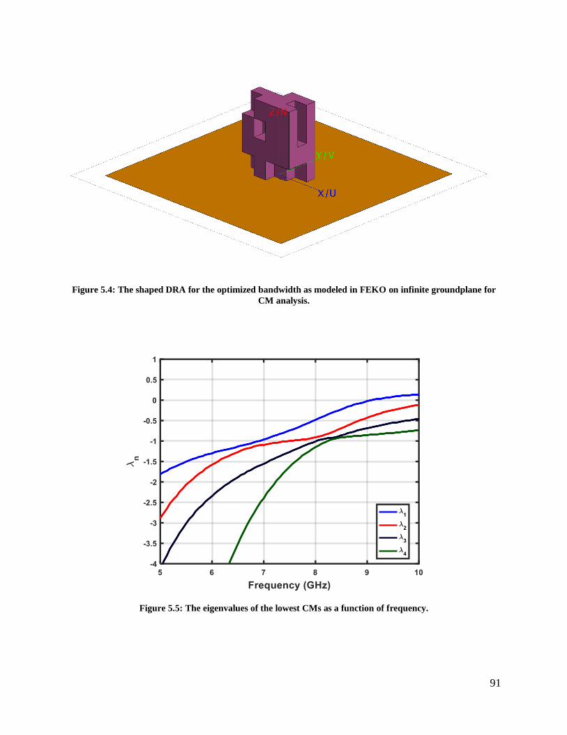
91
Figure 5.4: The shaped DRA for the optimized bandwidth as modeled in FEKO on infinite groundplane for
CM analysis.
Figure 5.5: The eigenvalues of the lowest CMs as a function of frequency.

92
(a) (b)
Figure 5.6: The electric fields (a) and magnetic fields (b) calculated at 7.5 GHz of CM #2 within (and just
outside) the shaped DRA in the plane normal to the infinite groundplane at z = 10 mm.
The MWCs of the lowest four CMs, with the surrogate source placed at maxr equal to
( )2.5,0.0,10.0 mm , are shown in Figure 5.7. There is a wide peak between 7 and 8 GHz, the
frequency range over which the coupling was optimized to ensure impedance matching potential
when a probe feed is inserted. There are MWC peaks at other frequencies that “were not requested”
via the fitness function, but this does not negate in any way the fact that we got what we asked for.
The additional coupling peaks will contribute to an even wider bandwidth beyond the frequency
range specified. By comparing Figure 5.5 to Figure 5.1, it is evident that a CM does not have to be
exactly at resonance for there to be good coupling to the surrogate source, at least not in this shaped
DRA case. The surrogate source placed was also placed the center (0.0 ,0.0,10.0) mm, which was
not the outcome of the shaping process, to illustrate that the amount of the power coupling into the
same mode could not be achieved as much as placing the surrogate source in the original position
which was the result of the optimization. The corresponding MWCs due to the source placed in
the center position are shown in Figure 5.7: the level of MWC is lower than the ones related to the
original position.

93
Figure 5.7: The MWCs of the lowest four CMs due to an infinitesimal electric dipole source positioned at
(2.5,0,10.0) mm (solid line) and positioned at (0,0,10.0) mm (dashed line).
Simulation and Measurement of the Completed DRA Antenna
Figure 5.8: The shaped DRA with a physical probe feed placed on a finite groundplane as modeled in FEKO.

94
The shaped DRA was then simulated in FEKO as a MoM driven problem in which the
standard SMA-sized coaxial probe as a source, a finite PEC ground plane, and dielectric losses41
were modeled; this is close to the state of the fabricated DRA. The FEKO model is shown in Figure
5.8. The CM analyses performed during the shaping process did not take into account the finite
ground plane, losses, and the actual physical feed mechanism. This will influence the 11S and
radiation pattern, and radiation efficiency of the DRA antenna, among other things. However, if
the finite ground is sufficiently electrically large, and the losses are reasonably low (as they usually
have to be in acceptable RF designs, the differences should not be that significant. The groundplane
dimensions are chosen to be 75 x 75 mm2, which is 1.75 x 1.75
in terms of the free-space
wavelength at the 7.5 GHz (the center frequency). A larger groundplane size would improve the
front-to-back ratio of the radiation pattern up to a certain point, but that would be at the expense
of the overall size of the antenna. The standard coaxial probe has a diameter of 1.27mm and 4.10
mm, respectively, and the insulating spacer has a dielectric constant of 2.33. This ensures a 50-
ohm characteristic impedance over the 1-20 GHz operating band of the coax. The model of coaxial
probe is shown in Figure 5.9; this same model will be used in the examples in Section 5.3 and
Section 5.4, except that the position and height of the probe might be different in these other
examples.
Figure 5.9: A plane cut in y-z to show the coaxial feed modeled in FEKO.
The model was used to perform a full-wave analysis of the simulated between 6 to 10 GHz to see
if those extra MWC peaks mentioned above appear at the outside specified 7 – 8 GHz frequency
range. The reflection coefficient was computed as a function of three different probe heights to
show that it is possible to match the impedance around the center frequency. Of course, this is only
possible because42 of the presence of the MWC peaks in Figure 5.10, the reflection coefficient is
41 As determined in Section 2.7. 42 As explained in the case studies in Section 4.4.

95
shown for the base of the probe feed positioned at43 (2.5,0.0) with heights of 6, 6.5 and 7 mm. We
can clearly see this impedance matching can be adjusted based on the desired center frequency. In
our case, a probe with a height of 6.5 mm is the one required since 7.5 GHz is the center frequency.
Indeed, with this probe height the bandwidth actually achieved is about 38%. Also, we show that
if the shaped DRA is fed in the center instead, then slightly less power coupling into the intended
CM as shown in Figure 5.7 by comparing it the feed’s location which is offset from the center.
This shows that the CM analysis provided the optimum location for the feed even though some
may think the center may be the best. In Figure 5.10, it is shown that feeding the structure in the
center provides slightly less bandwidth impedance the offset probe.
Figure 5.10: |S11| in dB at the probe port for the shaped DRA with coaxial cable fed at (2.5,0.0,0.0) mm as a
function of pin height (solid lines) fed at (0,0) mm (dashed line).
The radiation patterns of the shaped DRA, and the probe without the DRA present, are shown in
Figure 5.11 and Figure 5.12 for two different cuts. The maximum gain for the shaped DRA occurs
at 45 = , as depicted in Figure 5.13. The maximum gain for the probe with the DRA removed
occurs at 60 = . Clearly the probe is not the main contributor to the radiation pattern of the
antenna; the DRA modes are “kicking in” and forming the radiation pattern. For the shaped DRA,
a maximum gain (not realized gain) of 5 to 6 dBi can be achieved between 7 and 8 GHz which can
43 Although use of the surrogate infinitesimal dipole source in the shaping process revealed that it should be positioned
at ( )2.5,0.0,10.0 mm , practicalities dictate that the probe cannot start at 10z mm= but instead at 0z mm= (right at
the groundplane), and then extends upwards.

96
be achieved by the probe itself. The radiation efficiency is more than 97% over the entire frequency
range. Only dielectric losses were included via the loss tangent44 of 0.006, with the probe and
groundplane assumed to be PEC. This was simply done to show that even with the low-cost widely
available 3-D printing material used, a DRA antenna can be realized for which the DRA is not the
highest-loss part. As the setting shown Figure 5.14, the actual measurements of |S11| and radiation
pattern were performed and compared to the simulation results; the comparisons are shown in
Figure 5.15 for |S11| and Figure 5.16 and Figure 5.17 for the radiation pattern in two different cuts.
The measured and simulated results are in good agreement, and the slight discrepancies can be
attributed to various factors like the air gap between the probe and the DRA, the glue for holding
the DRA on the groundplane, imperfection in dimensions of DRA and probe, and finally
measurement instrument inaccuracy. The Agilent Technologies vector network analyzer (VNA),
model E5017C, was used throughout all the measurements, including the next two examples, for
both the reflection coefficient (|S11|) and the far-field anechoic chamber at Pennsylvania State
University .
Air gaps and bonding are some of the practical considerations mentioned in [PETO07, CH10], and
these are some of the factor in making a difference between the simulation and measurement
results, unless they are considered in the simulation model. It is rare that one considers these factors
in the simulation model since it is not possible to determine how much gap between the DRA and
the ground plane or between the DRA and probe prior the fabrication. Similarly, the permittivity
of bonding material might not be available and the thickness it would create can be difficult to
predict. However, a post simulation to the fabrication can be performed to confirm the cause of
any discrepancy.
44 As noted in Section 2.7.

97
Figure 5.11: The radiation pattern for no DRA present (blue line), and shaped DRA present (red line) at 7.5
GHz in the x-z plane
Figure 5.12: The radiation pattern for no DRA present (blue line), and shaped DRA present (red line) at 7.5
GHz in the y-z plane

98
Figure 5.13: The maximum gain as a function of frequency for the shaped at ( 45 , 180 ) = = , and
unshaped DRA at ( 45 , 180 ) = = and the probe without the DRA at ( 60 , 180 ) = = .
(a) (b)
Figure 5.14: (a) |S11| measurement setting. (b) Far-field radiation pattern measurement setting.

99
Figure 5.15:The measured result (dashed line) for |S11| in dB compared to simulated result (solid line) for the
shaped DRA with a probe height of 6.5 mm.
Figure 5.16: The measured result (dashed line) for the radiation pattern compared to simulated result (solid
line) for the shaped DRA with a probe height of 6.5 mm at 7.5 GHz for x-z plane.

100
Figure 5.17: The measured result (dashed line) for the radiation pattern compared to simulated result (solid
line) for the shaped DRA with a probe height of 6.5 mm at 7.5 GHz for y-z plane.

101
SHAPE SYNTHESIS EXAMPLE #2: 2-PORT MIMO DRA
Preamble
The use of MIMO systems as a means to increase channel capacity was briefly discussed in
Section 2.6. Such approaches use multi-antenna systems. In this shape synthesis example, we wish
to use a single DRA with two ports, so that it forms a 2-antenna system or, more simply put, a 2-
port MIMO antenna for operation at 2.4 GHz.
5.3.2 The Objective Function and Shaping Process
Designing a two-port MIMO antenna requires the excitation of two orthogonal (and hence
uncorrelated) modes at the same frequency. For this example, we propose the use of two different
types of feed. A coaxial probe of the type used in Example#1 as port#1, and a slot in the
groundplane (the slot being fed by a microstrip line) as port#2. The surrogate source used in the
shape synthesis will thus be an infinitesimal electric dipole for port#1, and an infinitesimal
magnetic dipole for port#2. In the context of CM analysis, if port#1 excites one set of CMs, and
port#2 excites a different set, then due to the CM far-zone field orthogonality properties the two
ports will be uncorrelated. We will shape synthesize the DRA to principally excite a single CM
when port#1 is turned on, and a different single CM when port#2 is turned on. Precisely where to
locate such ports must be found as part of the shaping process.
Similar to Example#1, with the intention of evaluating DRA shapes for CMs that will couple
strongly to a surrogate vertical infinitesimal electric dipole (denoted by ˆe for conciseness), we
define a term whose maximization will both identify a receptive mode (i.e. the value of q) and tell
us where to locate the surrogate ˆe at which it is receptive, namely
1
, 1
1,2,...
( ) 1( )
max ( ) 1
q
z qq
z normn
z nn
r
E r jE r
E r j
−
−
=
+=
+
(5.3-1)
, ( )n
z normE r is the vertical component of the fields normalized by the maximum vertical component
calculated at points r at the center of all voxels making up the starting geometry. The numerator
in (5.3-1) is the same as the selection factor defined in Example#1. The denominator does not
indicate that the optimization routine responsible for the overall shaping process is used to
maximize the quantity within the curly brackets. It says that for each population member, the
largest value of the quantity in curly brackets is found by examining its value for all modes
considered at each point at the center of all voxels. This normalization is necessary because we
will next define a quantity similar to (5.3-1), but in terms of the tangential magnetic field, and we
wish these quantities to have the same order of magnitude.

102
So, with the intention of evaluating the DRA shapes for CMs that will couple strongly to a
surrogate horizontal infinitesimal magnetic dipole (denoted by ˆm for conciseness) we define a
term whose maximization will both identify a receptive mode (i.e. the value if j) and where to
locate the surrogate ˆm at which it is receptive, namely the normalized horizontal component of
the magnetic fields
( )
( )
1
, 1
1,2,...
1( )
max 1
j j
x y jj
xy normn n
x y nn
r
H H jH r
H H j
−
−
=
+ +=
+ +
(5.3-2)
Then for each shape in the population of some generation, the points er and mr at which , ( )q
z normE r
and , ( )j
xy normH r are found to be maximum are identified. This identifies the i-th CM and its
receptive point er , and the j-th CM and its receptive point mr , for each population member. Since
the two eventual physical ports cannot be close to each other, to avoid direct mutual coupling, an
added constraint in this selection process that leads to the evaluation of the fitness function is that
the distance between er and mr are must be greater than / 4 , where is the free-space
wavelength at the intended frequency. If the latter condition fails to hold, then the searching will
locate the occurrence of the next largest value of either , ( )q
z normE r or , ( )j
xy normH r . We also ensure
that the mode indices mode indices i and j are not the same. In addition to the points at which the
sources are placed, the angle of which the surrogate magnetic dipole is to be oriented during the
selection referred to above is determined as 1tan
j
y
m j
x
H
H −
=
. The infinitesimal magnetic dipole
is always parallel to the groundplane since it is the surrogate source for the eventual physical slot
that lies in the x-y plane (that is, the groundplane).
For clarity, we repeat that the shape optimization algorithm does not maximize expressions (5.3-
1) and (5.3-2). These expressions are evaluated in finding the fitness function value for each
population member using the “maximum function” in MATLAB. In other words, they lie within
the fitness function definition.
The MWC (e ) due to an infinitesimal electric dipole ˆ
e placed at er , and separately, the MWC
(m ) due to an infinitesimal magnetic dipole ˆ
m placed at mr , are then calculated for all modes
for each population member. The quantity e for mode P1 (that excited by port#1) must be much
be higher than it is for mode P2 (that excited by port#2). This ensures that that mode P2 does not
get excited when you excite mode P1 (to maintain a low correlation). Similarly, the quantity m
for mode P2 must be much be higher than it is for mode P1, thereby ensuring that mode P1 does
not get excited when you excite mode P2. Hence, the ratios

103
, 2
, 1
e P
e
e P
= (5.3-3)
and
, 1
, 2
m P
m
m P
= (5.3-4)
must both be minimized. This is achieved by minimizing the composite objective function
_ __ (1 )F obj e F obj mF obj = + − (5.3-5)
where _F obj is the weight between (5.3-4) and (5.3-5). _F obj was chosen to be 0.5.
Parameter Settings for the Shaping Process
The starting shape in the optimization for the MIMO DRA antenna is a rectangular shape of
dimensions 62.5 mm x 39 mm x 15.6 mm, with a dielectric constant equal to 10. Fifty voxels of
dimensions 12.5 mm x 7.8 x 7.8 mm each were used to sub-divide the starting shape into shaping
boxes. The options for the GA optimization algorithm (listed in APPENDIX A) were chosen based
on multiple trial and error runs, and observation of the convergence success and computational
time, despite the fact we are not really concerned with coding efficiency here. A population number
of 100, and a maximum of 15 generations, were selected. However, only 7 generations were
actually used in order to minimize the fitness function in (5.3-5) because the optimization was
terminated due to the fact that the average change in the fitness value was less that the function
tolerance specified under the GA options. Figure 5.18 shows the expression (5.3-5) was minimized
to 0.0009 and the corresponding chromosome was of course then selected as the final shape. The
optimization run time was roughly 7 hours.

104
Figure 5.18: The best and mean values of the fitness function at every generation for Example#2.
Outcome of the Shaping Synthesis Process
The final shaped DRA is shown in Figure 5.19. It may have a number of significant CMs at
2.4 GHz, but the shape optimization process will have identified two specific modes, namely P1
and P2 (as defined in Section 5.3.2) and two locations points er and mr . Because of the way the
fitness functions have been defined, a ˆe placed at er will principally excite mode P1, whereas a
ˆm placed at er will principally excite mode P2. The field distributions of these two modes are
shown in Figure 5.20 and Figure 5.21.
The points er and mr were, respectively, found to be (-17.7,0,1.25) mm and (3.5,2.5,1.25) mm. The
distance between these two positions is definitely larger than / 4 , which will keep the undesired
mutual coupling between the two physical ports which are eventually to be placed around these
locations. The angle m for ˆ
m was found to be close to 19 degrees.
.

105
Figure 5.19: The shaped DRA for MIMO application placed on infinite ground plane.
(a) (b)
Figure 5.20: The electric fields (a) and magnetic fields (b) calculated at 2.4 GHz of CM # P1 within (and
just outside) the shaped DRA in the plane perpendicular to the infinite groundplane at a height of 1.25 mm.
(a) (b)
Figure 5.21: The electric fields (a) and magnetic fields (b) calculated at 2.4 GHz of CM #P2 within (and just
outside) the shaped DRA in the plane parallel to the infinite groundplane at a height of 1.25 mm.

106
By examining the MWC in Figure 5.22 and Figure 5.23, it is evident that CM #P1 (labelled CM#2
in the figure) is indeed excited strongly when ˆe was placed at er , as is CM #P2 (labelled CM#1
in the figure) when ˆm was placed at mr . If ˆ
e were to strongly excite both CM#P1 and CM #P2,
and ˆm were to strongly excite CM#P2, then the two mode sets excited at these ports would not
have orthogonal overall far-zone fields, and hence the two ports would not have low correlation.
Fortunately, the power coupling into modes other than CM#1 and CM #2 is negligible. For
example, one can see that some power is coupled into CM #3 if ˆe is active, but virtually none is
coupled into CM#3 when ˆm is active. Thus, the mode sets excited by the two surrogate sources
consist of different modes, thus keeping the eventual port correlations low. The peak of the MWC
due to ˆe excitation occurs at 2.44 GHz, whereas it occurs at 2.35 GHz when ˆ
m is on. Although
the two peaks do not coincide exactly at the specified frequency of 2.4 GHz, we nevertheless
anticipate the possibility of good impedance matching for both ports since the MWC peaks are
wide and encompass the 2.4 GHz point. This argument will be vindicated in Section 5.3.5 when
the completed DRA antenna is analyzed.
Before proceeding we draw the reader’s attention once more to the field distributions in Figure
5.20 and Figure 5.21. If the objective function were to be simplistically composed of (5.3-1) and
(5.3-2) only and did not consider the MWCs in the actual objective function as in (5.3-5), we would
conclude that CM#P2 would be the mode associated with ˆe excitation, and CM#P1 with ˆ
e
excitation. But this would be incorrect. Carefully thought out objective functions are essential. As
scores of users of optimization tools have confirmed, “you only get what you ask for”.

107
Figure 5.22: The modal weighting coefficients due to the electric dipole source only positioned at (-17.7,0,1.25)
mm for the shaped DRA shown in Figure 5.19.
Figure 5.23: The modal weighting coefficients due to the magnetic dipole source only positioned at
(3.5,2.5,1.25) mm for the shaped DRA shown in Figure 5.19.

108
Simulation and Measurement of the Completed DRA Antenna
The shaped DRA is then placed on a finite groundplane of size 150 x 110 mm2 and fed with
a coaxial probe (port 1) and a slot aperture coupled through a microstrip line (port 2). As shown in
Figure 5.24, the model in FEKO was set up as a driven problem using the MoM to solve for the
far fields, S-parameters, and ports’ related characteristics.
The probe axis was located at er = (-17.7, 0.0, 0.0) mm as “recommended” by the shape synthesis
result for good coupling. The probe’s specifications were made the same as the one used in
Example #1 in Section 5.2.5, except that the height of the probe (the extension of the inner
conductor) was adjusted to obtain the best impedance matching at port#1 at 2.4 GHz. A height of
11 mm provided the best results, as indicated by the fact that 11 -20dBS at 2.4 GHz in Figure
5.25.
Designing the slot feed at port 2 to have a low 22S is more complex than the design of the probe
feed at port 1, since more design variables are involved in creating it, such as the length and width
of slot, the length of the open stub beyond the slot, and the width of the microstrip line. The
starting design parameters for the slot feed were obtained using the analysis presented in
APPENDIX D and then optimized for best performance. When the slot was centered at mr = (3.5,
2.5, 0.0) mm as “recommended” by the shape synthesis result, the port-to-port coupling terms
21 12S S= were lower than -30dB, but it was not possible to obtain a good 11S . The latter only
proved possible with the slot centered at (6.0,5.0,0.0) mm, with the tilt angle of 19 degrees found
from the shape synthesis process discussed in the previous section. This provided 22 10dBS −
at 2.40 GHz, as shown in 22S . The FWB offered by port 1 and port 2, respectively, is 18.8% and
16.7 %. The port-to-port coupling terms 21 12S S= are approximately – 20 db. For MIMO
antennas, the ECC45 is one of the quantities of importance and must be lower than 0.5. In Figure
5.26, the ECC is found to be lowest at the desired frequency. 2.4 GHz, with a value of close to .001,
which is very satisfactory. The radiation pattern at each beam port is shown in Figure 5-24, and
they both resemble a broadside pattern. The details of the optimized 2-port MIMO antenna are
listed in Table 5-1.
The successful shaping process described above could be extended to have additional ports.
Although this will increase the complexity, the ideas used here in the construction of the 2-port
case objective function would still hold.
It was found out later that the amount of PREMIX 1046 material was not sufficient for printing the
dielectric resonator with such proposed dimensions to resonate at 2.4 GHz; however, since we are
not set on that resonant frequency as we are only trying to prove a concept, it was necessary to
45 This was defined in Section 2.6. 46 A 3-D printer filament sample given by PREMIX Group and was characterized and discussed in Section 2.8

109
(a)
(b)
Figure 5.24: (a) The shaped 2-port MIMO DRA modeled in FEKO. (b) A plane cut in x-z of the geometry
exposing the probe and the tilted slot within the shaped DRA.

110
scaled the dimensions down in order to use the same material without affecting the EM properties
of the structure. According to the theorem of similitude as discussed in Section 3.4.4, scaling down
all the dimensions of the DRA only causes a shift in frequency up by factor of the same amount
(inversely proportional). It was determined by scaling the dimensions by a factor of 0.686 would
allow us use the same material, and consequently, the center frequency (and all other frequencies)
should be shifted from 2.4 to 3.5 GHz. The scaling was only applied to the dielectric resonator not
the feeding structure whose design parameters were tweaked to adapt to the new scaled dielectric
resonator; all the new scaled values are listed in Table 2-1. By comparing Figure 5.24 and Figure
5.28, one can see that the simulation result for S-parameters are basically shifted from one
frequency to the other; the discrepancies in S-parameters levels was due to tweaking the feeding
elements which cannot done by a linear scaling. In Figure 5.28, the simulation and measurement
results for S-parameters are compered: a significant shift at higher frequency (4.05 GHz) for the
S11 dip was notice and slight shift in S22 curve. The significant shift in S11 can be attributed to the
larger diameter (and possibly height) of the gap in the DRA for fitting the probe; unlike example
1, a hole was drilled to fit the soldered probe. Other than that, we found that the simulation and
measurement results are in good agreement. Having said that, a minimum return loss of 10 dB was
acquired around the center frequency. Both the radiation pattern of two different cuts for port 1
and 2 are respectively depicted in Figure 5.29 and Figure 5.30; again, there was a slight
discrepancy between the simulated and measured results.
Table 5-1: The design parameters of the shaped MIMO DRA in FEKO model.
Design Parameters Variable Name in
FEKO
Value Scaled
Value
Unit
Ground plane width along x
direction
grnd_l 110 75.5 mm
Ground plane length along y
direction
grnd_w 150 102.8 mm
Ground plane thickness N.A. infinitesimal - N.A.
Microstrip feed width along x feed_w 1.9 2.0 mm
Microstrip feed length along y feed_l 71.8 52.4 mm
Microstrip feed line thickness N.A. infinitesimal - N.A.
DRA width along y dr_w 62.5 42.9 mm
DRA depth along x dr_l 39 26.8 mm
DRA height along z dr_h 15.6 10.7 mm
DRA dielectric constant epsr_DRA 2.98 2.98 N.A.
DRA loss tangent loss_DRA 0.004 0.004 S/m
Substrate height along z Substrate_thickness 0.508 0.508 mm
Substrate dielectric constant epsr_Subs 2.2 2.2 N.A.
Substrate loss tangent loss_Subs 0.001 0.001 S/m
Stub length Stub_l 3 3 mm
Slot Length ap_l 20 20 mm
Slot width ap_w 3.6 3.6 mm
Slot center along x OffsetX 6 6 mm
Slot center along y OffsetY 5 5 mm
Slot tilt angle (from x axis) phi_m 19 19 degrees

111
Figure 5.25: S-parameters (in dB) for the shaped MIMO DRA antenna
Figure 5.26: ECC values computed from the S-parameters for the shaped MIMO DRA.
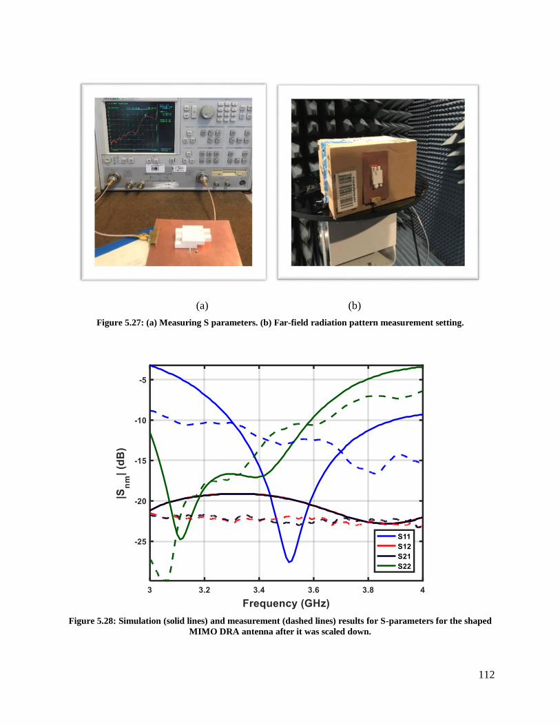
112
(a) (b)
Figure 5.27: (a) Measuring S parameters. (b) Far-field radiation pattern measurement setting.
Figure 5.28: Simulation (solid lines) and measurement (dashed lines) results for S-parameters for the shaped
MIMO DRA antenna after it was scaled down.

113
(a) (b)
Figure 5.29: The measured result (dashed line) for the radiation pattern compared to simulated result (solid
line) of port 1 for the shaped DRA 3.5 GHz for (a) x-z plane and (b) y-z plane.
(a) (b)
Figure 5.30: The measured result (dashed line) for the radiation pattern compared to simulated result (solid
line) of port 2 for the shaped DRA 3.5 GHz for (a) x-z plane and (b) y-z plane.

114
SHAPE SYNTHESIS EXAMPLE #3: BROADSIDE PATTERN AND
RESTRICTED SIZE DRA
Preamble
As wireless communication devices such as cell phones, Wi-Fi routers, and laptops are
becoming smaller in size and lighter in weight, so designing compact components is essential. One
such component in the front end of any wireless communication system is the antenna(s). The
maximum antenna size can be one constraint due to the limited space in many wireless devices, in
addition to the accessibility of a feed point to the antenna, especially with congested electronic
sub-systems. Therefore, in this example we assume a DRA is to be shaped to satisfy the following
three requirements of an imaginary client:
1) The antenna must be excited by a simple feed structure that does not require a substrate
since we assume the chassis is used as a groundplane. This means only a probe can be employed
as the physical feed mechanism. The client is really looking to save on space, and material (i.e.
cost) and reduce feeding complexity.
2) The antenna must have a broadside radiation pattern as the antenna is located in the middle
of a device. A broadside pattern is something more challenging to design when a probe is used to
excite DRAs, especially if they are not cylindrical.
3) The antenna must fit inside the volume constraint depicted in Figure 5.31. The feed must
be also positioned within the space specified.
4) The antenna must operate at 2.65 GHz with a minimum return loss of 10 dB at the center
frequency. An unusually wide bandwidth is not a requirement for this shape synthesis case.

115
Figure 5.31: The dimensions of the volume within which the antenna and its feed mechanism may be placed.
The Objective Function and Shaping Process
The fitness function must be so defined that its minimization results in a DRA antenna that
satisfies the four requirements listed in Section 5.4.1. During the shape optimization process, for
each population member that is “bred”, the CM analysis is performed to find a mode whose far-
zone eigenfields represent a broadside pattern, and that can be excited by a probe feed. Modes with
broadside patterns can be identified as those for which the quantity
,max
( , )
(0,0)
max ( , )
nn
far
n
Ee
E
= (5.4-1)
is unity. Quantity nE is the far-zone eigenfield of the n-th mode. The denominator examines the
far-zone field of the n-th mode over all directions ( , ) in the hemisphere above the infinite
groundplane. As always, the total scattered47 in the far-zone consists of two components
( ) ( ) ( )( ) ( )ˆ ˆ, , ,n n
nE E E = + (5.4-2)
47 Once again, we note that (as indicated in Section 4.5) although this is the scattered field, it will be the dominant
contributor to the total field in any proper design because of strong coupling to the DRA modes.
20 m
m

116
and hence ( , )nE is calculated as
( ) ( ) ( )2 2
( ) ( ), , ,n n
nE E E = + (5.4-3)
Several modes could have a broadside pattern, but we need to select that one which has the largest
1
, 1
1,2,...
( ) 1( )
max ( ) 1
q
z qq
z normn
z nn
r
E r jE r
E r j
−
−
=
+=
+
(5.4-4)
where ( )q
zE r is the z-component of the electric near field of the q-th CM evaluated at position r
. The “find the largest” operation in the denominator of (5.4-4) is only taken over those modes
with broadside patterns. For each population member, use of (5.4-4) then selects a particular
broadside mode, and its point er at which , ( )q
z normE r is largest at which to place a surrogate
infinitesimal electric dipole.
The MWCs of all modes (with or without broadside patterns) due to an infinitesimal electric dipole
( ˆe ) placed at the above-determined location
er are then calculated at the center frequency and a
frequency on either side of it. Three frequency points are the minimum number to spot a peak
which an indication of best modal coupling48.
The objective function evaluated for each population member is then
_i
i
j
j
F obj
=
(5.4-5)
where they i are the MWCs related to the modes with non-broadside patterns and the j MWCs
related to the modes with broadside patterns49.
48 In the numerical example to be shown we did this at the centre frequency and frequencies 100 MHz on either side
of it. 49 Although a specific broadside mode was selected to determine
er , all broadside modes are welcome to assist in
providing the broadside pattern of the final antenna.

117
The objective function in (5.4-5) is not evaluated if the mode with the highest MWC peak does
not have a broadside pattern. Instead, the objective function is assigned a value of 1 (a large value,
intended to discourage its retention into the next generation)
Parameter Settings for the Shaping Process
The starting shape shown in Figure 5.31, with a relative permittivity of 7.5, was divided into sixty
voxels, each of dimensions 8 x 8 x 6.67 mm, as illustrated in Figure 5.32. This makes the length
of the chromosome equal to 60 bits representing each voxel to be considered in the shaping process
through the GA process. As in Example#2, the options for the GA optimization (listed in
APPENDIX A) were selected based on multiple trial and error runs, and observation of the
convergence success and computational time, despite the fact we are not really concerned with
coding efficiency here. A population number of 50, and maximum number generations of 40, were
selected, but only 11 generations were needed in order to minimize the objective function in
(5.4-5), as the optimization was terminated due to the fact that the average change in the fitness
value became than the function tolerance specified in the GA option. Figure 5.33 shows that
expression (5.4-5) was minimized to a value of 0.0030, and the corresponding chromosome was
selected as the final DRA shape. The mean values of the fitness function are high because of its
being assigned of 1 whenever an MWC peak occurs for a CM with a non-broadside pattern. The
optimization run time was roughly 16 hours and 25 minutes.
Figure 5.32: The starting shape is divided to 60 voxels of size 8 x 8 x 6.67 mm, with a dielectric constant of 7.5

118
Figure 5.33: The best and mean values of the fitness function at every generation, for Example#3.
Outcome of the Shape Synthesis Process
The shaping process succeeded in synthesizing a DRA that can be fed by a vertical probe, and
yet provide a broadside radiation pattern, at 2.65 GHz. The shaped DRA fits entirely within the
limited space specified. The shaped DRA is shown in Figure 5.34,, and the optimum location for
the surrogate source ˆe was determined to be
er = (16.0, 8.0, 3.33) mm. The MWCs in this case
are those shown in Figure 5.35. The synthesis process has clearly so shaped the DRA that only50
CM#1, CM#2 and CM#3 51 couple strongly to the surrogate source located at er . The far-zone
eigenfields of these particular modes are shown in Figure 5.36.
50 These are not necessarily the CMs with the lowest resonance frequencies. 51 These are not necessarily the CMs with the lowest resonance frequencies.

119
Figure 5.34: The shaped DRA placed on infinite ground plane and fed with an infinitesimal electric dipole
positioned at er = (16.0, 8.0, 3.33) mm.
From one can clearly see that CM #1 is the most “purely-broadside” mode, and it couples the most
strongly of all modes to the surrogate source at the specified frequency of 2.65 GHz, as desired.
The modal electric and magnetic fields of CM#1 within the DRA are those in Figure 5.37 shows
why this is so; the z-component of the electric field is large (has a “hot spot”) at location er . As a
matter of interest, we refer to the modal fields of CM#2 shown in Figure 5.38 at 2.45 GHz (as
opposed to 2.65 GHz). This shows that, at this frequency, there is hot spot of the z-directed electric
field at er for CM#2. This is the reason that there is a peak in the MWC of CM#2 at 2.45 GHz, as
shown in Figure 5.35.
Figure 5.35: The modal weighting coefficients for the shaped DRA shown in Figure 5.34.

120
(a) (b)
(c)
Figure 5.36: The far-zone modal fields for CM#1 (a) CM #2 (b) CM #3 (c) calculated at 2.65 GHz.
(a) (b)
Figure 5.37: The electric fields (a) and magnetic fields (b) calculated at 2.65 GHz of CM #1 within (and just
outside) the shaped DRA in the plane perpendicular to the infinite groundplane at height of 3.33 mm.

121
(a) (b)
Figure 5.38: The electric fields (a) and magnetic fields (b) calculated at 2.45 GHz of CM #2 within (and just
outside) the shaped DRA in the plane perpendicular to the infinite groundplane at height of 3.33 mm.
Simulation and Measurement of the Completed DRA Antenna
Figure 5.39: The FEKO model of the shaped DRA for a broadside pattern application, fed with a coaxial
probe and placed on a finite ground plane.
Similar to what was done in Examples #1 and #2, and for the same reasons, the shaped DRA
in this example was modeled in FEKO as a driven problem using the MoM, as shown in Figure
5.39. The groundplane size is 150 x 150 mm. The height of the probe was tuned for best impedance
matching at 2.65 GHz; it was found to be 11.5 mm. In Figure 5.40, the computed |S11| is plotted in
dB from 2 to 3 GHz. At the target frequency of 2.65 GHz we have |S11|<-30 dB. This of course the
frequency at which we have the MWC peak for CM#1, and in line with the conjecture we made in

122
Section 4.4, it was expected that excellent matching could be achieved there. In passing52, we note
that the fractional impedance bandwidth is more than 20%.
Figure 5.40: The magnitude of S11 (in dB) for shaped the DRA with restricted size and broadside pattern.
An additional goal was to have the DRA antenna radiate a broadside pattern. The computed pattern
in Figure 5.42, and Figure 5.43 at 2.65 GHz, shows that this is indeed broadside in both cuts. We
mention in passing that, at 2.65 GHz, the computed maximum gain was found to be 5.6 dBi, the
front-to-back ratio more than 9 dB, and the radiation efficiency53 more than 96%. Both the
simulated and measured results for S11 and radiation pattern shown in Figure 5.40Figure 5.42 and
Figure 5.43 are in good agreement.
(a) (b)
Figure 5.41: (a) Measuring S parameters. (b) Far-field radiation pattern measurement setting.
52 We say “in passing” because bandwidth did not form part of the objective function. 53 Assuming losses in the dielectric material only.

123
Figure 5.42: The measured result (dashed line) for the radiation pattern compared to simulated result (solid
line) for the shaped DRA 2.65 GHz for x-z plane.
Figure 5.43: The measured result (dashed line) for the radiation pattern compared to simulated result (solid
line) for the shaped DRA 2.65 GHz for y-z plane.

124
CONCLUSIONS
Although the material in Chapter 3 represents several original contributions to the theory of
characteristic modes generally, the main purpose of this work was to clear the ground for the
correct use and understanding of the characteristic modes of dielectric resonator antennas. Chapter
4 developed the machinery for a computational electromagnetics-based tool capable of performing
the shape synthesis of DRA antennas. As an essential part of this tool, it introduced the concept of
using surrogate sources with characteristic modal analysis so that the shape synthesis can be done
without having to specify the location of the actual physical feed mechanism beforehand. This
showed what the broad principles should be for the construction of the complicated objective
functions (needed for use of optimization algorithms as the driver of the shape synthesis process).
These objective functions need to be customized depending on the particular requirements
(“specs”) that the shaped DRA antenna must satisfy.
Here in Chapter 5 we presented three specific DRA antennas successfully shaped synthesized
using the tool described in Chapter 4. This is the very first time DRA antennas have been shape
synthesized, and thus the procedure can safely be qualified by the adjective “novel”.
The first example is the least “tough” of the three. However, it served the purpose of showing how,
without having to perform approximate calculations on the NM frequencies (due to the difficulty
in doing so numerically), a CM-based shaping approach can be used to automatically give us the
DRA that does what we need. We are no longer bound to the use of conventional DRA shapes,
and need not have to use cut-and–try largely experimental methods on regularly stepped or other
shapes when the conventional shapes fail to satisfy the design conditions.
The second example is a DRA that has been shaped to act as a two-port MIMO antenna, with one
port’s physical feed mechanism being dictated to be a slot and the other a probe, and with broadside
radiation patterns. Exciting non-overlapping sets of CMs ensures a low ECC between the two ports
(that is, two antennas sharing the single DRA structure).
The third example demonstrates how a non-standard starting shape, which could represent a
constraint on the region the final antenna may occupy on some wireless device being designed,
can be used to provide an antenna with favorable performance which nevertheless satisfies the
above space constraint. The shape synthesis approach allows the designer to come up with the best
design under externally imposed limitations as far as DRA antennas are concerned.
None of the examples have shapes like any other DRA antenna reported in the literature.

125
CHAPTER 6: GENERAL CONCLUSIONS
It has been said that the ideal antenna synthesis procedure would allow one to “start with a set
of electrical, mechanical, and system specifications that would lead to a particular antenna together
with its specific geometry and material specification”, but that “this ideal general antenna synthesis
method does not exist” [STUT 08]. In this chapter we will summarize how the work in this
dissertation has contributed to the goal of reaching the above ideal situation through its
development of a new shape synthesis technique for DRA antennas.
The principal original contributions to antenna shape synthesis which have been presented in this
dissertation can be described as follows:
• An approach was devised for the three-dimensional shape synthesis of dielectric resonator
antennas which are subject to geometry restrictions (e.g. must fit within a specified region
of space). It is entirely new, representing the first time any three-dimensional shape
optimization of dielectric resonator antennas has been described. It is particularly novel
because, not only does it shape the dielectric material, but it permits the shape optimization
process to proceed without the restriction of a pre-determined feed-point location.
Although the feed mechanism type must be chosen prior to commencement of the shaping
process, the feed-point location is determined as part of the shape synthesis process. This
removes restrictions on the shaping process.
• The approach was made possible through properly connecting antenna performance
parameters to characteristic mode concepts. If this has not been worked out, the feed
location could not be part of the outcome of the synthesis procedure but would have to be
specified beforehand. This would reduce the design freedom of the shaping procedure.
Instead, use of the characteristic modes allows the computation of modal weighting
coefficients using the surrogate source idea that was established. These coefficients are
then used in the definition of the objective functions.
• The shape synthesis technique was successfully applied to three dielectric resonator
antenna examples, each with different design requirements and constraints. Its success in
these cases demonstrates the effectiveness of the new shaping technique. Computed
performance is supported by experimental results.
• The implementation of the shaping tool itself, apart from being needed to validate the
shaping process, is an addition in its own right. It has purposefully been fully implemented
using commercially available software, for the computational electromagnetics, the
optimization algorithm, and the controller that manages the shaping process and allows communication between the various steps. The advantage of being able to use such
commercial codes is that the approach at once becomes more accessible to others.
Some of the lesser contributions of the dissertation, although still significant, are as follows:
• A more robust method for tracking the characteristic modes of dielectric objects.

126
• The presentation of a more general (broadened) formulation of the sub-structure
characteristic mode concept.
• Formal mathematical proofs of the orthogonality properties of sub-structure modes.
There remains one issue, and one completely new application, whose investigation in the future
would prove useful:
• The incorporation of different material relative permittivities as additional shape
optimization variables. In this dissertation it has been assumed that the dielectric resonator
is homogeneous. It would appear that 3D printers that can lay down several different
dielectric materials, albeit not yet widespread, will soon be available. This would make the
suggested extension worthwhile. It would unfetter the synthesis process still further.
• Now that a tool is available for shape synthesizing dielectric objects generally, it could be
used as the basis for the shape synthesis of dielectric transmitarray antennas. The relatively
large electrical size of such antennas might at present make such an application.
• Further enhancements on the objective functions, refinements on GA options, and the use
of different voxel shapes other than the rectangular block are some of the extra work can
be done in the future. Also, developing an optimization algorithm that understands the EM
and geometry restrictions better, instead of using the GA, is to be implemented for more
robust and efficient shaping process.

127
REFERENCES
[AKKE05] K. Akkerman ,The analysis and Control of Radiation from Conducting
Structures using Characteristic modes, Master’s Thesis, Dept. Electrical
and Computer Engineering, University of Houston, USA, 2005.
[ALMP08] G.Almpanis, C.Fumeaux and R.Vahldieck, “The Trapezoidal Dielectric
Resonator Antenna”, IEEE Trans. Antennas Propagat., Vol.56, No.9, pp.
2810-2816, Sept.2008.
[ALRO13] H. Alroughani, An Appraisal of the Characteristic Modes of Composite
Objects, Master’s Thesis, University of Ottawa, Canada, 2013.
[ALRO14] H. Alroughani, J. Ethier and D. A. McNamara, "Observations on
computational outcomes for the characteristic modes of dielectric objects",
IEEE Int. Antennas Propagat. Symp. Digest , pp. 844-845, Memphis, USA,
July 2014.
[BALA05] C.A.Balanis, Antenna Theory (Wiley, 2005).
[BALA08] C.A.Balanis, Modern Antenna Handbook (Wiley, 2008)
[BERN14] T.Bernabeu-Jiménez, A.Valero-Nogueira, F.Vico-Bondia, E.Antonino-
Daviu and M.Cabredo-Fabres, “A 60 GHz LTCC rectangular dielectric
resonator antenna design with characteristic mode theory”, IEEE Int.
Antennas Propagat. Symp. Digest, pp.1928-1929, Memphis, USA, 2014.
[BERN15] T.Bernabeu-Jiménez, A.Valero-Nogueira, F.Vico-Bondia, A.Vila-
Jiménez, D.Sánchez-Escuderos and F.Gallée, “A 60 GHz coplanar-
waveguide-fed slot-coupled rectangular DRA using the theory of
characteristic modes”, European Conference Antennas and Propagat,
Lisbon, Portugal, April 2015.
[BERN18] T.Bernabeu-Jiménez, A.Valero-Nogueira, F.Vico-Bondia and A.A.Kishk,
“Internal natural resonances prediction through the theory of characteristic
modes”, Radio Science, Vol.53, pp.397-405, April 2018.
[BLAD07] J. van Bladel, Electromagnetic Fields (IEEE Press, 2007) 2nd Edition.
[BUCC90] O.M.Bucci, G.Franceschetti, G.Mazzarella and G.Panriello, "The
intersection approach to array synthesis", Proc. Inst. Elec. Eng., Pt.H,
Vol.137, pp.349-357, 1990.
[CABE07] M.Cabedo-Fabres, E.Antonino-Daviu, A.Valero-Nogueira and
M.F.Bataller, "The theory of characteristic modes revisited : A
contribution to the design of antennas for modern applications”, IEEE
Antennas Propagat. Mag.,Vol.49, pp.52-68, Oct. 2007.
[CAPE11] M. Capek, P. Hazdra, and J. Eichler, “A Method of Tracking Characteristic
Numbers and Vectors”, Progress EM. Research B, Vol. 33, pp. 115-134,
2011.
[CHAI07] R. Chair, A.A. Kishk and K.F. Lee, “Wideband stair-shaped dielectric
resonator antennas”, IET Microw. Antennas Propagat., Vol.1, No.2, pp.
299–305, 2007.

128
[CHAN77] Y. Chang, R.F. Harrington, “A Surface Formulation for Characteristic
Modes of Material Bodies”, IEEE Trans. Antennas Propagat., Vol. 25, No.
6, pp 789 – 795, November 1977.
[CHAN05] B. Chantraine-Bares, R. Sauleau, L. Le Coq and K. Mahdjoubi, "A new
accurate design method for millimeter-wave homogeneous dielectric
substrate lens antennas of arbitrary shape", IEEE Trans. Antennas
Propagat., vol. 53, no. 3, pp. 1069-1082, March 2005.
[CHEN04] L.-F. Chen et al., Microwave Electronics Measurement and Materials
Characterization, New York, NY, USA: Wiley, 2004.
[CHEN14] Y.Chen and C.Wang, “Surface integral equation based characteristic mode
formulation for dielectric resonators”, IEEE Int. Antennas Propagat. Symp.
Digest, pp.846-847, Memphis, USA, 2014
[CHEN15] Chen, Y. and Wang, C.-F. (2015) Characteristic Mode Theory for
Dielectric Resonators, in Characteristic Modes: Theory and Applications
in Antenna Engineering, John Wiley & Sons, Inc, Hoboken, NJ.
[CHEN16] Chen, Y. "Alternative surface integral equation-based characteristic mode
analysis of dielectric resonator antennas." IET Microwa. Antennas
Propagat.1, Vol. 0.2, p.p.193-201, 2016.
[CWIK89] T.Cwik, J.Patterson and T.Lockhart, “Constructing matrix Green's
functions for radiation and scattering problems”, IEEE Int. Antennas
Propagat. Symp. Digest, Vol.2, pp.586 – 589, 1989.
[ETHI09a] J. Ethier and D.A. McNamara, “The use of generalized modes in the design
of MIMO antennas”, IEEE Trans. Magnetics, vol. 45, no. 3, pp. 1124 –
1127, Mar. 2009.
[ETHI10a] J. Ethier and D. McNamara, “A Modal Significance Measure in the
Characteristic Mode Analysis of Radiating Structures”, Electronics
Letters, Vol. 46, No. 2, January 21, 2010.
[ETHI12a] J. Ethier & D.A. McNamara, "A Sub-Structure Characteristic Mode
Concept for Antenna Shape Synthesis", Electronics Letters, Vol.48, No.9,
April 2012.
[FEKO] FEKO, EM Software & Systems Inc. (www.feko.info).
[GARB65] R.J.Garbacz, “Modal Expansions for Resonance Scattering Phenomena,”
Proceedings of the IEEE, pp. 856 – 864, August 1965.
[GARB82] R.J.Garbacz and D.Pozar, "Antenna shape synthesis using characteristic
modes", IEEE Trans. Antennas Propagat., Vol.30, No.3, pp.340-350, May
1982
[GAST 67] M.Gastine, L.Courtois and J.L.Dormann, “Electromagnetic resonances of
free dielectric spheres”, IEEE Trans. Microwave Theory Tech., Vol.15,
No.12, pp.694-700, Dec.1967.
[GLIS 83] A.W.Glisson, D.Kajfez and J.James, “Evaluation of modes in dielectric
resonators using a surface integral equation formulation”, IEEE MTT-S
Digest, pp.409-411, 1983.
[GORO03] Gorokhov, D.A.Gore, and A.J.Paulraj, “Receive antenna selection of MIMO flat-fading channel Theory and and algorithms, ” IEEE Trans.
Inform. Theory, vol.49, pp.2867-2896,Oct.2003.

129
[GUAN16] L.Guan, D.Ding, Z.Fan, M.Li, Z.Li and R.Chen, “Analysis of dielectric
resonator antennas using characteristic modes”, IEEE/ACES International
Conf. Wireless Information Technology Systems Applied Comp. EM.
Honolulu, USA, March 2016.
[HAKK60] B. W. Hakki and P. D. Coleman, "A Dielectric Resonator Method of
Measuring Inductive Capacities in the Millimeter Range", IRE Trans.
Microw. Theory Tech., vol. 8, no. 4, pp. 402-410, July 1960.
[HARR 61] R.F.Harrington, Time-Harmonic Electromagnetic Fields (McGraw-Hill,
1961).
[HARR71a] R.F.Harrington and J.R.Mautz, “Theory of Characteristic Modes for
Conducting Bodies,” IEEE Transactions on Antennas and Propagation,
Vol. AP-19, No. 5, pp. 622 – 628, September 1971.
[HARR71b] R.F.Harrington and J.R.Mautz, “Computation of Characteristic Modes for
Conducting Bodies,” IEEE Transactions on Antennas and Propagat, Vol.
AP-19, No. 5, pp. 629 – 639, September 1971.
[HARR72] R. F. Harrington, J. Mautz, Y. Chang, “Characteristic Modes for Dielectric
and Magnetic Bodies,” IEEE Transactions on Antennas and Propagation,
Vol. AP-20, No. 2, pp. 194 – 198, March 1972.
[HFSS] HFSS, ANSYS Inc., USA (www.ansys.com).
[HUIT12] L. Huitema and T. Monediere, Dielectric Materials for Compact Dielectric
Resonator Antenna Applications (open source book, 2012)
[JAKO00] U.Jakobus, “Comparison of different techniques for the treatment of lossy
dielectric/magnetic bodies within the method of moments formulation”,
AEÜ Int. J. Electron. Commun., Vol.54, No.1, 2000.
[JIN02] J.Jin, The Finite Element Method in Electromagnetics (Wiley, 2002)
[KAJF 84] D.Kajfez, A.W.Glisson & J.James, “Computed modal field distributions
for isolated dielectric resonators”, IEEE Trans. Microwave Theory Tech.,
Vol.32, No.12, pp.1609-1616, Dec.1984.
[KAJF83] D.Kajfez, A.W.Glisson & J.James, “Evaluation of modes in dielectric
resonators using a surface integral equation formulation”, IEEE Trans.
Microwave Theory Tech., Vol.31, No.12, pp.1023-1029, Dec.1983.
[KHAL10] M.Khalily, M.K.A.Rahim and M.R.Kamarudin, “A novel p-shape
dielectric resonator antenna for wideband application”, IEEE Asia-Pacific
Conf. Applied EM, 2010.
[KISH01] Kishk, A.A., Glisson, A.W., and Junker, G.P, “Bandwidth enhancement
for split cylindrical dielectric resonator antennas’, J. Electromagnetics
Waves Appl., 2001, 15, (6), pp. 777–778.
[KISH02] Kishk, A.A., Yin, Y., and Glisson, A.W.: ‘Conical dielectric resonator
antennas for wide-band applications’, IEEE Trans. Antennas Propag.,
2002, 50, (4), pp. 469–474
[KISH03b] A. A. Kishk, ‘‘Wide-band truncated tetrahedron dielectric resonator
antenna excited by a coaxial probe,’’ IEEE Trans. Antennas Propag.,
vol.51, pp. 2913---2917, Oct. 2003. [KUCH00a] A.A.Kucharski, “Resonances in heterogeneous dielectric bodies with
rotational symmetry – Volume integral-equation formulation”, IEEE Trans.
Antennas Propagat., Vol.48, No.5, pp.766- 770, May 2000.

130
[LIAN08] X. L. Liang and T. A. Denidni, "H-Shaped Dielectric Resonator Antenna for
Wideband Applications," IEEE Antennas Wireless Propagat. Lett., vol. 7,
pp. 163-166, 2008
[LIAN09] X. L. Liang, T. A. Denidni and L. N. Zhang, "wideband l-shaped dielectric
resonator antenna with a conformal inverted-trapezoidal patch feed", IEEE
Trans. Antennas Propagat., vol. 57, no. 1, pp. 271-274, Jan. 2009.
[LIAN17] R. Lian, J. Pan and S. Huang, "Alternative surface integral equation
formulations for characteristic modes of dielectric and magnetic bodies",
IEEE Trans. Antennas Propagt, vol. 65, no. 9, pp. 4706-4716, Sept. 2017. [LIU01] Y. Liu, S. Safavi-Naeini, S. Chaudhuri, and R. Sabry, “On the Determination
of Resonant Modes of Dielectric Objects using Surface Integral Equations”,
IEEE Transactions On Antennas And Propagation, Vol.52, No.4, April 2001
[LIU 04] Y.Liu, S.Safavi-Naeini, S.K.Chaudhuri and R.Sabry, "On the
determination of resonant modes of dielectric objects using surface integral
equations", IEEE Trans. Antennas Propagat., Vol.52, pp.1062-1069, 2004.
[LI05] Bin Li and Kwok Wa Leung, "Strip-fed rectangular dielectric resonator
antennas with/without a parasitic patch," IEEE Trans. Antennas Propagat.,
vol. 53, no. 7, pp. 2200-2207, July 2005.
[LONG83] S. Long, M. McAllister and Liang Shen, "The resonant cylindrical
dielectric cavity antenna", IEEE Trans. Antennas and Propagat., Vol. 31,
no. 3, pp. 406-412, May 1983.
[LUDI14] D. J. Ludick, J. V. Tonder and U. Jakobus, "A hybrid tracking algorithm
for characteristic mode analysis", Int. Conf. Electromagnetics Advanced
Applications (ICEAA), Aruba, pp. 455-458, Aug. 2014.
[MATLAB] MATLAB, Matrix Mathematic Language Software.
(www.mathworks.com)
[MIER15] Z. Miers and B. K. Lau, "Wideband Characteristic Mode Tracking
Utilizing Far-Field Patterns", IEEE Antennas and Wireless Propagat. Let.,
vol. 14, no. , pp. 1658-1661, 2015.
[MIER17] Z. Miers and B. K. Lau, "On characteristic eigenvalues of complex media
in surface integral formulations", IEEE Antennas Wireless Propagat. Let.,
vol. 16, pp. 1820-1823, 2017
[MONG93] R.K.Mongia, and P.Bhartia, “Dielectric Resonator Antennas- A Review
and General Design Relations for Resonant Frequency and Bandwidth”,
Int. J. Microw. Mill.-Wave Comput.-Aided Eng., Vol. 4, No. 8, pp.230-247,
1993
[NAYE14] P. Nayeri et al., "3-D Printed Dielectric Reflectarrays: Low-Cost High-
Gain Antennas at Sub-Millimeter Waves",IEEE Trans. Antennas
Propagat., vol. 62, no. 4, pp. 2000-2008, April 2014.
[NOBL69] B.Noble, Applied Linear Algebra (Prentice-Hall, 1969)
[PETE97] A.Peterson, S.Ray and R.Mittra, Computational Methods for
Electromagnetics (IEEE Press, 1997).
[PETO10] A. Petosa and A. Ittipiboon, "Dielectric Resonator Antennas: A Historical
Review and the Current State of the Art," in IEEE Antennas and
Propagation Magazine, vol. 52, no. 5, pp. 91-116, Oct. 2010
[PETO07] A. Petosa, Dielectric Resonator Antenna Handbook (ARTECH House,
2007)

131
[POPO81]
B.D.Popovic, “Electromagnetic field theorems”, IEE Proc., Vol.128, Pt.A,
No.1, pp.47-63, Jan.1981
[QU14] S. W. Qu, H. Yi, C. H. Chan and K. B. Ng, "Low-cost discrete dielectric
terahertz lens antenna using 3-D printing," IEEE Conf. Antenna
Measurements Applications, Antibes Juan-les-Pins, 2014.
[RAIN12] B. Raines, and Roberto Rojas, “Wideband Characteristic Mode Tracking”,
IEEE Trans. Antennas Propagat., Vol. 60, No. 7, pp.3537-3541, July 2012.
[RICH39] D.Richtmyer, “Dielectric resonators”, J.Appl.Phys., Vol.10, pp.391-398,
June 1939.
[ROSE05] K.Rosengren, P.S Kildal., “Radiation efficiency correlation diversity gain
and capacity of a six-monopole antenna array for a MIMO system: theory,
simulation and measurement in reverberation chamber”, IET Microw.
Antennas and Propaga. , Vol. 152 ,pp.7-16, 2005.
[SCHA84] D.H.Schaubert, D.R.Wllton, and A. W.Glisson, "A Tetrahedral Modeling
for Electromagnetic Scatterlngby Arbitrary Shaped Homogeneous
Dielectrlc Bodies", IEEE Trans. Antennas Propagat., Vol. AP-32. pp 77-
85, 1984.
[SINC48] G.Sinclair, “Theory of models of electromagnetic systems”, Proc.IRE,
Vol.36, pp.1364-1370, 1948.
[STAE94] D.H.Staelin, A.W.Morgenthaler and J.A.Kong, Electromagnetic Waves
(Prentice-Hall, 1994) Chap.8
[STUT08] W.Stutzman and S.Licul, “Synthesis Methods for Antennas” in
C.A.Balanis (Edit.), Modern Antenna Handbook (Wiley, 2008) pp.631.
[TRIN16] S. Trinh-Van, Y. Yang, and K. Lee, K. Hwang, “A wideband circularly
polarized pixelated dielectric resonator antenna”, Sensors, Basel,
Switzerland, 2016.
[WU17] Q.Wu, “Computation of characteristic modes for dielectric bodies using
volume integral equation and interpolation”, IEEE Antennas Wireless
Propagat. Lett., Vol.16, pp.2963-2966, 2017.
[VOLA07] J.L.Volakis (Edit.), Antenna Engineering Handbook (McGraw-Hill, 2007)
[YAGH 81] A.D.Yaghjian, “Augmented electric- and magnetic-field integral
equations”, Radio Science, Vol.16, No.6, pp.987-1001, Nov.-Dec. 1981.
[YANG07]
L. Yang, A. Rida, R. Vyas, and M. M. Tentzeris, “RFID tag and RF
structureson a paper substrate using inkjet-printing technology,” IEEE
Trans. Microw. Theory Tech., vol. 55, no. 12, pp. 2894–2901, Dec. 2007.
[YANG17] B.Yang & J.J.Adams, “Quality factor calculations for the characteristic
modes of dielectric resonator antennas”, US National Committee of URSI
,Boulder, USA, Jan. 2017.
[ZOU16] M. Zou, J. Pan, D. Yang and G. Xiong, “Investigation of dual-band
omnidirectional rectangular dielectric resonator antenna”, EM Waves
Appl., 30:11, 1407-1416, 2016.

132
APPENDIX A: OPTIONS FOR GENETIC ALGORITHM
The genetic algorithm optimization function is a built-in function within the computation
package MATLAB, and it has the friendly-user options which can be used. The options are
somewhat different for the three examples discussed in CHAPTER 5:, so refer to the following
tables to see the type of functions used:
Table 0-1: The type of options selected for GA function for optimizing the DRA shape in example 1.
Option Name Value/Type Description/ Note
Population Type Bit String Every bit in the chromosome signifies a block in the
structure: 1 signifies block presence and 0 absence.
Population Size 100 The number of individuals.
Initial Population Specified Initial geometry from a previous optimization run
was used in the final optimization.
Scaling Function Proportional “The scaling function converts raw fitness scores
returned by the fitness function to values in a range
that is suitable for the selection function.
Proportional makes the expectation proportional to
the raw fitness score” 54.
Selection Factor Tournament “Selects each parent by choosing individuals at
random” the default number (4) was selected.
Reproduction Elite count Five elite individual with best fitness scores survive
to the next generation.
Mutation function Uniform “Mutation functions make small random changes in
the individuals in the population, which provide
genetic diversity and enable the genetic algorithm to
search a broader space.”. Uniform was selected since
54 The content is taken from MATLAB description of each option listed in GA function.

133
it does not make a difference since 0 and 1 are used
here
Mutation Rate 0.01 The default value was used.
Crossover Scattered This combines two parents to produce a new
individual for the subsequent generation. A random
binary is created. If the random vector has “1” then
it take a gene from the first parent and if “0” it takes
it from the second parent.
Migration Both Both is the migration of the nth subpopulation
migrates into both the (n–1)th and the (n+1)th
subpopulation. This intends to move individual
between subpopulations.
Migration Fraction 0.2 The default value was used.
Generation 10 Number of specified generations.
Stall Generation 2 “If the average change in the fitness function value
over Stall generations is less than Function
tolerance, the algorithm stops”.
Function Tolerance 1e-6 The default value was used.

134
Genetic algorithm’s options are the same for example 2 as example 1 except the ones listed in the
following table.
Table 0-2: The type of options selected for GA function for optimizing the DRA shape in example 2.
Option Name Value/Type Description/ Note
Generation 10 The same description is shown in
Genetic algorithm’s options are the same for
example 2 as example 1 except the ones listed in the
following table.
Table 0-2.
Genetic algorithm’s options are the same for example 3 as example 1 except the ones listed in the
following table.
Table 0-3: The type of options selected for GA function for optimizing the DRA shape in example 3.
Option Name Value/Type Description/ Note
Population Size 50 The number of individuals.
Generation 40 The same description is shown in
Genetic algorithm’s options are the same for
example 2 as example 1 except the ones listed in the
following table.
Table 0-2.
Stall Generation e The same description is shown in
Genetic algorithm’s options are the same for
example 2 as example 1 except the ones listed in the
following table.
Table 0-2.

135
APPENDIX B: THE FIELDS OF INFINITESIMAL
ELECTRIC DIPOLE
An infinitesimal electric dipole is an electric current density whose volume electric current
density
ˆ( , , ) ( ) ( ) ( )oJ x y z A z x y z = (A.B-1)
In the above expressions the term )()( yx makes the source a filament located on the z-axis. The
direction of the current is the positive z-direction, as dictated by the unit vector z . The factor )(z
ensures that the source is of infinitesimal length. This is illustrated in Figure 0.1As the final step
in our interpretation of (A.B-1) we wish to establish what the units are of the constant oA . We
know that the volume current density ( , , )J x y z has the units of amperes/metre2. The units of each
of the delta functions is the reciprocal of its argument, in other words (meter)-1. Hence oA has the
units of ampere-meter, and so it is a current moment. It is for this reason that engineers sometimes
write o eA I L= to emphasize that it is the current moment of an infinitesimal element of length
L with uniform electric current eI on it. The reader must remember that the infinitesimal dipole
is a theoretical construct though, and even very short dipoles do not in reality have uniform current
distributions.
The fields of an infinitesimal electric current element located at the origin, and oriented parallel to
the z-axis, are [HARR 61]
0
2 3
1 1( , , ) cos
2
jkror
AE r e
r jkr
− = +
(A.B-2)
0
2 2 3
1 1 1( , , ) sin
4
jkroj kAE r e
r jkr k r
− = + −
(A.B-3)
( , , ) 0E r = (A.B-4)
( , , ) 0rH r = (A.B-5)
( , , ) 0H r = (A.B-6)
2
1 1( , , ) sin
4
jkrojkAH r e
r jkr
− = +
(A.B-7)
with o ok = . Poynting’s theorem can then be used to show that total radiated power from
the infinitesimal dipole is
22
2
2
3
o o
rad
AP
= (A.B-8)

136
Y
X
Z
r
Observation
Point
ˆep
Figure 0.1: z -Directed Infinitesimal Electric Dipole Located at the Origin of the Chosen Coordinate System
The Fields of Infinitesimal Magnetic Dipole
The fields of an infinitesimal magnetic current element located at the origin, and oriented
parallel to the z-axis, are obtained from those of the infinitesimal electric current by applying the
duality theorem [HARR 61] to obtain
1
0
2 3
1 1( , , ) cos
2
jkror
AH r e
r jkr
−−
= +
(A.B-9)
1
0
2 2 3
1 1 1( , , ) sin
4
jkroj k AH r e
r jkr k r
−−
= + −
(A.B-10)
( , , ) 0H r = (A.B-11)
( , , ) 0rE r = (A.B-12)
( , , ) 0E r = (A.B-13)
2
1 1( , , ) sin
4
jkrojkAE r e
r jkr
− = − +
(A.B-14)
oA now has the units of volt-meter, since it is a magnetic current moment. It is for this reason that
people sometimes write o mA I L= to emphasize that it is the current moment of an infinitesimal
element of length L with uniform magnetic current mI on it. An appeal to the surface equivalence
theorem reveals [HARR 61] that an infinitesimal magnetic dipole can be used to represent a very
small slot radiator in an infinite PEC groundplane.

137
APPENDIX C: PROOFS OF THE ORTHOGONALITY
PROPERTIES OF SUB-STRUCTURE
CHARACTERISTIC MODES
These are the mathematical proofs of the orthogonality properties of such-structure modes that are
listed in Section 3.2.7. Matrix properties used can be found in [NOBL 69].
A. Property#1
Statement
[ ] [Z ][ ] (1 )Asub H Asub sub
m sub n n mnJ J j = + (A.C-1)
Proof
This follows directly from the eigenvalue problem (3.2-12) and the fact that [Z ]sub is symmetric,
using a procedure similar to that in [HARR71a] for conventional CMs. Since [ ]Asub
mJ is real
(equiphase), (3.2-16) can be written in two parts as
[ ] [ ][ ]Asub H sub Asub
m n mnJ R J = (A.C-2)
and
[ ] [X ][ ]Asub H sub Asub sub
m n n mnJ J = (A.C-3)
This assumes that the currents have been so normalized that each sub-structure mode radiates 1
watt, since (A.C-2) is also an expression for the power radiated by the n-th mode when we set
m n= in the expression.
Significance
As with conventional CMs, arbitrary surface currents on Object A (in the presence of Object B)
can be expanded in terms of sub-structure CM currents of Object A, allowing one to perform this
expansion without needing to expand the currents on the secondary Object B.
B. Property#2
Statement
Bsec Bsec
[ ] [ ][Z ] (1 )
[ ] [ ]
HAsub Asub
fs subm n
n mn
m n
J Jj
J J
= +
(A.C-4)
Proof
Bsec
Bsec
[ ][ ] [ ]
[ ]
HAsub
Asub H Hm
m m
m
JJ J
J
=
(A.C-5)
Using (3.2-4) and (A.C-5)in (A.C-4) yields

138
fs fs
Bsec AA AB
Bsec Bsec Bsecfs fs
BA BB
[ ] [ ] [ ][ ] [ ][Z ] [ ] [ ]
[ ] [ ] [ ][ ] [ ]
HAsub Asub Asub
fs Asub H Hm n n
m m
m n n
J J JZ ZJ J
J J JZ Z
=
(A.C-6)
If we carry out all the matrix multiplications in (A.C-6) we obtain
Bsec Bsec
fs fs Bsec
AA AB
Bsec fs Bsec fs Bsec
BA BB
[ ] [ ][Z ]
[ ] [ ]
[ ] [ ][ ] [ ] [ ][ ]
[ ] [ ][ ] [ ] [ ][ ]
HAsub Asub
fsm n
m n
Asub H Asub Asub H
m n m n
H Asub H
m n m n
J J
J J
J Z J J Z J
J Z J J Z J
= +
+ +
(A.C-7)
Next we replace Bsec
nJ by its expression given in (3.2-16), and similarly for Bsec
mJ . This gives
( ) ( )
Bsec Bsec
1fs fs fs fs
AA AB BB BA
1 1fs fs fs fs fs
BB BA BA BB BA
[ ] [ ][Z ]
[ ] [ ]
[ ] [ ][ ] [ ] [ ]
[ ][ ]
HAsub Asub
fsm n
m n
Asub H Asub Asub H Asub
m n m n
HAsub Asub Asub
m n m
J J
J J
J Z J J Z Z Z J
Z Z J Z J Z Z J
−
− −
= −
− + 1
fs fs fs
BB BB BA
IdentityMatrix
[ ]H
Asub
nZ Z Z J−
(A.C-8)
From (A.C-1) the term on the 2nd line of (A.C-8) is just (1 )sub
n mnj + . Inspection of the 3rd line of
(A.C-8) shows it to be zero (the terms cancel each other). Thus (A.C-5) is proved.
Significance
The combined currents on Object A and Object B satisfy the orthogonality properties; in other
words, the current on Object B does not break the properties expected of CMs.
C. Property#3
Statement
Bsec Bsec
[ ] [ ][ ]
[ ] [ ]
HAsub Asub
fsm n
mn
m n
J JR
J J
=
(A.C-9)
Proof
Since Bsec[ ]nJ can be complex, we cannot obtain (A.C-9) by merely taking the real and imaginary
parts of each side of (A.C-5). Instead we use the fact that
1
[R ] [Z ] [Z ]2
fs fs fs H= + (A.C-10)
and so

139
Bsec Bsec Bsec Bsec Bsec Bsec
[ ] [ ] [ ] [ ] [ ] [ ]1 1[ ] [Z ] [Z ]
2 2[ ] [ ] [ ] [ ] [ ] [ ]
H H HAsub Asub Asub Asub Asub Asub
fs fs fs Hm n m n m n
m n m n m n
J J J J J JR
J J J J J J
= +
(A.C-11)
+
We know from (A.C-5) that the 1st term in (A.C-11) is simply (1 )sub
n mnj + , and proceed to work
on the 2nd term. We have [HARR72, pp.24]
fs fs fs fs
AA AB AA BA
fs fs fs fs
BA BB AB BB
[ ] [ ] [ ] [ ][ ]
[ ] [ ] [ ] [ ]
HH H
fs H
H H
Z Z Z ZZ
Z Z Z Z
= =
(A.C-12)
Then using (A.C-6) and (A.C-12), and performing all the matrix multiplications, we obtain the 2nd
term on the right-hand side of (A.C-11) as
Bsec Bsec
fs fs Bsec
AA BA
Bsec fs Bsec fs Bsec
AB BB
[ ] [ ][Z ]
[ ] [ ]
[ ] [ ] [ ] [ ] [ ] [ ]
[ ] [ ] [ ] [ ] [ ] [ ]
HAsub Asub
fs Hm n
m n
Asub H H Asub Asub H H
m n m n
H H Asub H H
m n m n
J J
J J
J Z J J Z J
J Z J J Z J
= +
+ +
(A.C-13)
Next, we again replace Bsec
nJ by its expression given in (3.2-16), and similarly for Bsec
mJ . We
then carry out all the resulting matrix multiplications and use the fact that 1
fs fsBB BB[ ]
HHZ Z
− is the
identity matrix due to the fact that fsBB[ ]Z is symmetrical. This provides us with the intermediate
result
1fs fs fs fsAA BA BB ABBsec Bsec
[ ] [ ][Z ] [ ] [ ] [ ]
[ ] [ ]
HAsub Asub H
Hm nfs H Asub H H H Asub
m n
m n
J JJ Z Z Z Z J
J J
− = − (A.C-14)
The term
1 1fs fs fs fs fs fs fs fsAA BA BB AB AA AB BB BA[ ] [ ] [ ] [ ] [ ]
H HH
H H HsubZ Z Z Z Z Z Z Z Z
− − − = − = (A.C-15)
since from (3.2-11) we know that fs fs fs 1 fs
sub AA AB BB BA[ ] [ ] [ ][ ] [ ]Z Z Z Z Z−= − , and have the property
[HARR72,pp.11] that for any three matrices ( )[ ][ ][ ] [ ] [ ] [ ]H H H HA B C C B A= . So, we have shown thus
far that
Bsec Bsec
[ ] [ ][Z ] [ ] [ ] [ ]
[ ] [ ]
HAsub Asub
fs H Asub H H Asubm n
m sub n
m n
J JJ Z J
J J
=
(A.C-16)

140
Therefore, from (A.C-11),
( )
Bsec Bsec
2[R ]
[ ] [ ][R ]
[ ] [ ]
1 1[ ] [Z ][ ] [ ] [Z ] [ ]
2 2
1[ ] [Z ] [Z ] [ ]
2sub
HAsub Asub
fsm n
m n
Asub H Asub Asub H H Asub
m sub n m sub n
Asub H H Asub
m sub sub n
mn
J J
J J
J J J J
J J
= +
= +
=
(A.C-17)
as required, the final step resulting from the use of (A.C-1).
Significance
Comparison of the results (A.C-1) and (A.C-17) shows that the current on Object B does not
contribute to the radiated power - it just redistributes it. This is to be expected since the CM current
on the Object A is the only “source”. The currents on Object B are not new sources of power. They
are just secondary to Asub
nJ which “already knows” about secB
nJ . The cancelling effect of the terms
in (24) occurs because the power coupled to the object B is negative, but then re-radiates and
becomes positive again and we have the power balance. In other words, whatever power Object B
sinks from Object A will inevitably be re-radiated because Object B is a PEC structure (and hence
does not dissipate power).
D. Property#4
\
Statement
Bsec Bsec
[ ] [ ][X ]
[ ] [ ]
HAsub Asub
fs subm n
n mn
m n
J J
J J
=
(A.C-18)
Proof
This follows by substituting [ ] [ ] [ ]fs fs fsZ R j X= + in (A.C-9), multiplying the resulting matrices,
using result (A.C-9), and comparing left and right hand sides of the expression.
E. Property#5
Statement
The far-zone fields of the sub-structure CMs are orthogonal over the sphere at infinity, and so
satisfy a relation identical to (3.2-8).
Proof Because of (A.C-4), (A.C-9) and (A.C-18), the proof of this statement follows that described in
[HARR 71a] for conventional CMs.

141
APPENDIX D: THE GUIDELINES IN DESIGNING THE STARTING
GEOMETRY OF THE SSLOT APERTURE ANTENNA AS A FEED
As stated in [PETO07], simple equations to design a slot aperture antenna for feeding DRAs
do not exist; however, there are some guidelines that can be followed for a starting geometry which
can then be optimized. A sketch of the feeding geometry is shown in Figure 0.1 in which the
necessary dimensions are outlined.
Figure 0.1: The feeding structure of the aperture slot fed by a microstrip line. [PETO07]
In order for the slot not to resonate within the band of operation, the slot length sl is chosen
carefully, but large enough for a good coupling to the DRA. For a good starting value,
0.4 o
s
e
l
= (A.D-1)
where
2
s re
+= (A.D-2)
and s rand are the dielectric constant of the substrate and dielectric resonator, respectively. The
slot width sw should not be too wide to prevent a large backlobe, and its value should be around
0.2s sw l= (A.D-2)

142
The width is usually varied between 0.15 sl to 0.25 sl . The length of the open stub (the extension of
microstrip line beyond the slot) is chosen in the way the reactance part of the slot is canceled for a
better matching. The length
4
gs
= (A.D-3)
where g is the guided wavelength in the substrate. Finally, the width of microstrip line is
determined based on the dielectric constant of the substrate, thickness of the substrate, and
frequency for 50-ohm impedance matching since a 50-ohm port is usually used [BALA05]. The
software “TxLine” (which is an open source software) is used to determine the appropriate line
width

VITA
Hamad Alroughani
Education: ▪ University of Ottawa: Bachelor degree in Electrical Engineering Sept. 2007 – July 2011
▪ University of Ottawa: Master degree in Electrical Engineering Sept. 2011 – Oct. 2013
▪ Pennsylvania State University: Ph.D. degree in Electrical Engineering Sept. 2014 – Aug. 2018
Experience:
▪ Volunteered in the microwave lab at University of Ottawa Jan. -Apr., 2011
▪ Worked as undergraduate research assistant at University of Ottawa May-Aug., 2011
▪ Worked at the Embassy of Kuwait in Ottawa Jan. -Aug., 2014
▪ Worked as a grader at Pennsylvania State University Aug.,2014- May 2018
▪ Reviewed several papers in various journals 2015- Present
Publication and Conferences ▪ H.Alroughani et al., “An appraisal of the characteristic modes of dielectric object”, IEEE
Symp. on Ant. and Prop. & USNC/URSI National Radio Science Meeting, Chicago, USA, July
2012.
▪ H.Alroughani, An Appraisal of the Characteristic Modes of Composite Objects, Master’s
Thesis, University of Ottawa, Canada, 2013.
▪ H.Alroughani et al., “On the classification of characteristic modes, and the extension of sub-
structure modes to include penetrable material”, Proc. ICEAA '14 / IEEE APWC '14 Symp.,
Aruba, August 2014.
▪ H.Alroughani et al., “Observations on computational outcomes for the characteristic modes
of dielectric objects”, IEEE AP-S Int. Symp. Digest, Memphis, Tennessee, USA, July 2014.
▪ H.Alroughani, "Studying microstrip patch antennas using the theory of characteristic modes",
IEEE AP-S Int. Symp. Digest, Vancouver, Canada, pp. 1476-1477, July 2015.
▪ H.Alroughani et al., “On the orthogonality properties of sub-structure characteristic modes”,
Microwave & Optical Technology Letters, Vol.58, No.2, pp.481-486, Feb.2016.
▪ H.Alroughani et al., “Clarifications on the surface integral equation computation of the
characteristic modes of dielectric objects”, IEEE AP-S Int. Symp. Digest, San Diego, USA,
July 2017.
▪ H.Alroughani, "An enhanced algorithm in tracking characteristic modes of dielectric objects",
Applied Computational Electromagnetics Symp., Florence, Italy, April 2017.
▪ H.Alroughani et al., “Numerical experiments in tracking the characteristic modes of dielectric
objects”, 2016 IEEE/ACES International Conference on Wireless Information Technology
and Systems (ICWITS) and Applied Computational Electromagnetics (ACES) Symp. Digest,
Honolulu, Hawaii, USA, March 2016.
▪ H.Alroughani et al., “Sorting the characteristic modes of PEC objects not electrically small”,
12th European Conference on Antennas and Propagation (EuCAP 2018), London, UK, April
2018.
Related Documents