University of Groningen Faculty of Mathematics and Natural Sciences Zernike Institute for Advanced Materials The renaissance of multiferroics: bismuth ferrite (BiFeO 3 ) – a candidate multiferroic material in nanoscience. By: Seva (Vsevolod) V. Khikhlovskyi Top Master in Nanoscience S1951971 [email protected] Supervisor: Dr. Graeme Blake Department of Chemical Physics Zernike Institute for Advanced Materials Groningen June 2010

Welcome message from author
This document is posted to help you gain knowledge. Please leave a comment to let me know what you think about it! Share it to your friends and learn new things together.
Transcript

University of Groningen Faculty of Mathematics and Natural Sciences
Zernike Institute for Advanced Materials
The renaissance of multiferroics: bismuth ferrite (BiFeO3) – a candidate multiferroic material in nanoscience.
By: Seva (Vsevolod) V. Khikhlovskyi Top Master in Nanoscience
S1951971 [email protected]
Supervisor: Dr. Graeme Blake
Department of Chemical Physics Zernike Institute for Advanced Materials
Groningen June 2010

Seva V.V.Khikhlovskyi June 2010
Abstract
Multiferroics are materials that exhibit two or more primary ferroic order parameters simultaneously. The definition of multiferroics can be expanded to include other types of long-range order such as antiferromagnetism (a non-primary order parameter). Nowadays, multiferroism often refers to any combination of ferroelectricity and magnetism (both ferromagnetism and antiferromagnetism) in one particular material. Multiferroics are currently attracting considerable attention - they are promising materials for new types of devices. The current paper presents a basic overview of multiferroic materials in general, but it is mainly focused on one particular multiferroic material - bismuth ferrite (BiFeO3 or BFO). BFO is perhaps the only material that is both magnetic and strongly ferroelectric at room temperature. As a result, it has had a great impact on the field of multiferroics. Both the basic physics and device applications of BiFeO3 are discussed, with a view to use in spintronics and memory devices that can be addressed both electrically and magnetically. It has been shown that different types of BFO nanostructures can be produced such as thin films, nanoparticles, nanopowders, nanotubes and nanowires using different techniques including pulsed laser deposition (PLD), RF magnetron sputtering, chemical vapor deposition (CVD) and metal-organic CVD (MOCVD), chemical solution deposition (sol-gel) and molecular beam epitaxy (MBE). As prepared BFO nanostructures possess many new properties (for instance, the appearance of ferromagnetism and enhanced ferroelectricity) compared to bulk BFO samples. This paper is focused mainly on the magnetic properties of such nanostructures and their application to real devices. There are at least two theories that explain the appearance of ferromagnetism, based on the ideas of uncompensated surface spins and interruption of the spiral spin structure found in the bulk. It seems that the two theories simply complement each other. Nevertheless, BFO nanostructures are attracting much attention as a core part of novel devices such as spin valve structures, barrier layers in spintronics, tunneling magnetoresistance, and potential logic and memory devices. At the end of the literature review, a perspective on multiferroics is given. Despite the fact that there are many different review papers concerning BFO, none of them describe all of the types of preparation techniques available or all of the nanostructures that are possible. Thus, the main aim of this paper is to eliminate this lack of knowledge.

Seva V.V.Khikhlovskyi June 2010
Table of contents
1. Introduction………………………………………………………………………………………......1 2. Brief theory:
2.1. Ferroelectricity………..…………………………………………………………………………2 2.2. Ferromagnetism, antiferromagnetism………………………………………..………………….4
2.3. Multiferroism………………………………………………………………..…………………..5 3. Structure of BiFeO3……...…………………………………………………………………………...6 4. Fabrication, properties and possible applications of different multiferroic BiFeO3 nanostructures: 4.1. Thin films…………………………………………………………….………………………….9 4.2. Nanoparticles, nanopowders………………………………………….………………………..15 4.3. Nanotubes, nanowires, nanofibers……………………………………………………………..18 4.4. Possible applications of BiFeO3 nanostructures…………………………….…………………21 5. Conclusions………………………………………………………………………………………….24 6. Acknowledgements………………………………………………………………………………….25 7. References…………………………………………………………………………………………...25

Seva V.V.Khikhlovskyi June 2010
Page 1
1. Introduction.
Materials that exhibit both magnetic and electrical ordering have become a hot topic of research in recent years (fig. 1). The link between magnetic and electric properties potentially allows the creation of novel devices if magnetic and electric order can be mutually controlled. The Maxwell equations that relate electric and magnetic fields, charge density and current density show that magnetic and electric interactions couple to each other. The formal equivalence of the equations of electrostatics and magnetostatics explains numerous similarities in the theory of ferroelectrics and ferromagnets, for instance their behavior in external fields (fig. 2) and domain structures (fig. 3). These similarities are unexpected because of the
different origins of ferroelectricity and magnetism in solids. Magnetism appears in materials which have incomplete ionic shells whereas ferroelectricity originates from atomic shifts that break inversion symmetry in a crystal. Multiferroic materials possess two or more primary ferroic properties in the same phase. However, today the definition of multiferroics has been expanded to include other long-range orders, for instance antiferromagnetism (fig. 4). Thus, any material that combines more than one of these properties is described as multiferroic. Nowadays, multiferroism often refers to a combination of ferroelectricity and magnetism (ferromagnetism, antiferromagnetism) in one particular material. Magnetoelectric switching in multiferroics can only be done if the magnetization and polarization are strongly coupled, which is a very unusual phenomenon. In 1959 Landau and Lifshitz pointed out the theoretical possibility of coupling magnetic and electric degrees freedom in one material [4]. Such materials have magnetization that is proportional to an applied electric field and polarization proportional to magnetic field. Later, Dzyaloshinskii predicted [5] and Astrov observed [6] this type of coupling, which is now known as the linear magnetoelectric effect. The next step was an attempt to create a novel material possessing at least two types of ordering – ferromagnetism and ferroelectricity. This was achieved by Soviet scientists [7]. However, the study of multiferroics was virtually stopped soon afterwards. It should be noted that only very few multiferroics are linear magnetoelectrics (there are strict crystal symmetry requirements), and higher-order coupling terms usually dominate. An increase of interest in multiferroics started again around 2003. Some main reasons for this include: - the discovery of magnetically induced ferroelectricity. Here, spin frustration often causes spiral antiferromagnetic ordering that induces ferroelectricity [8];
Figure 1. Number of papers from 2003-2009 containing keyword “multiferroic” (as cited by Web of Science).
Figure 2. Typical (a) ferroelectric hysteresis loop. (b) ferromagnetic hysteresis loop.
Figure 3. Magnetic domains of Fe (100) [1]. Ferroelectric domains in NaKNbO3 [2].
Figure 4. Multiferroics combine the properties of ferroelectrics and magnets [3].

Seva V.V.Khikhlovskyi June 2010
Page 2
- more accessible high power computational systems for modeling multiferroics such as density-functional theory and combinations of a variety of other advanced methods and algorithms. These include for example LDA (local density approximation)/GGA (Generalised Gradient Approximations) approaches, LSDA (local spin-density approximation) + U (Coulomb interaction), Berry-phase approach and many more; - advances in thin film (atomic- and nano- scale) growth techniques; - new experimental methods that allow the observation of magnetic and electric domains; - recent successes in the synthesis of complex oxides have brought research to a new level, in which complex artificial oxide structures can be realized with atomic-level precision; - multiferroics have become materials with promising future applications (digital technologies etc.). Materials with pronounced magnetic and electronic properties permeate everywhere in modern technology and life. The current trend towards device miniaturization has led to interest in combining electronic and magnetic properties into multifunctional, multiferroic materials. The magnetoelectric effect would form the basis of a new type of devices for electric field-controlled magnetic memory data storage. Multiferroics are attractive not only because they have the properties of both magnetic and ferroelectric compounds, but also because the magnetoelectric coupling leads to additional functionality. However, the application of these materials is still a big question because the magnetoelectric coupling is too weak, making it very difficult to perform switching; furthermore, the polarization or magnetization are often too small and the temperatures at which these types of ordering occur are too low. Therefore, the development of new materials is very necessary. One of the most studied and promising multiferroic materials to date is bismuth ferrite (BiFeO3), which has a relatively simple structure and at the same time uncommon properties: bismuth ferrite possesses two coupled order parameters - ferroelectricity and antiferromagnetism at room temperature [9, 10]. Moreover, bismuth ferrite sets a standard in the global search for new multiferroic materials. Nevertheless, even in bismuth ferrite the magnetoelectric coupling is weak. However, in 2003, Ramesh’s group successfully created epitaxial BiFeO3 multiferroic thin film heterostructures [11] that possess greatly enhanced multiferroic properties. These films display a room-temperature spontaneous polarization that is almost an order of magnitude higher than that of the bulk. Therefore, the creation and development of artificial nanoscale structures is very promising.
Thus, multiferroic materials hold the future for ultimate nanodevices and are hence very interesting for theoretical and practical research, especially in nanoscience.
2. Brief theory.
The first two sections of the current chapter present briefly theories of ferroelectricity as well as ferromagnetism, since ideal multiferroic materials possess simultaneously both types of ordering. However, antiferromagnetism (AFM) is also considered because BiFeO3 possesses AFM as well as ferroelectricity. The last part is focused on the origin of multiferroism and the properties of multiferroic materials.
2.1. Ferroelectricity.
Ferroelectricity was discovered in 1921 by Valasek in the U.S. A ferroelectric is a material which undergoes a phase transition from a high-temperature, high-symmetry (paraelectric) structure that is an ordinary dielectric to a low-temperature, low-symmetry (ferroelectric) structure that has spontaneous macroscopic electric polarization. The polarization is reversible, non-volatile and its direction can be switched by applied field. In other words, ferroelectric crystals can be seen as an assembly of batteries with a particular orientation, which remains stable unless an external electric field is applied to change its direction (fig. 5). Polarization arises below a certain phase transition temperature called the Curie temperature - Tc. The spontaneous polarization of ferroelectric materials implies a hysteresis effect. The concept of electric polarization is the key to understanding ferroelectricity. Ferroelectrics also behave as high dielectric-constant insulators useful in the development of capacitors and energy storage materials.
Figure 5. Schematic view of ferroelectricity.
Figure 6. Schematic view of the perovskite oxide structure.

Seva V.V.Khikhlovskyi June 2010
Page 3
The most widely studied and used ferroelectrics today are perovskite-structure oxides, ABO3 (fig. 6), which possess a prototypical cubic structure at high temperature. The cubic perovskite structure is characterized by a small cation, B, at the center of an octahedron of oxygen anions, with large cations, A, at the unit cell corners. A structural distortion from a high symmetry type to a low symmetry type occurs below the Curie temperature. This distortion is accompanied by an off-center shift of the small cation, which is the major factor giving rise to the spontaneous polarization. There are a few different mechanisms that cause ferroelectricity: - ferroelectricity in multiferroic perovskites. The off-center shifts of the transition metal ion cause ferroelectricity in these systems. This ion is thought to form strong covalent bonds with one (or even three) oxygens, using its empty d-states. However, the theory for this case has not yet been made clear. - ferroelectricity caused by stereochemically active lone pair cations, e.g. Bi3+ or Pb2+ in BiFeO3 or PbVO3 (fig. 7). These divalent ions have two 5s or 6s electrons that do not participate in chemical bonding. Cations containing a 5s
(6s) lone pair of valence electrons usually break local inversion symmetry. The small B cation in ferroelectric perovskite oxides lowers its energy by shifting along one of the [111] directions (fig. 8). This structural modification leads to a system with a “double-well” shaped potential energy (fig. 9), which describes the position of the small cation as a function of distance between the oxygen anions. - ferroelectricity due to charge ordering, often observed in transition metal compounds. This mechanism works in compounds like LuFe2O4. - geometric ferroelectricity, where the structural instability is driven by size effects or by other geometrical considerations (fig. 10). For example ferroelectricity in YMnO3 is caused by tilting of the MnO5 unit and as a result the oxygen ions move closer to the small Y ions.
Figure 7. In BiFeO3 the ordering of lone pairs (yellow ”lobes”) of Bi3+ ions (orange), contributes to the polarization (green arrow) [12].
Figure 8. PbTiO3 possess a rhombohedrally distorted perovskite structure, where all ionic sublattices are displaced relative to each other along the polar (111) direction, and the oxygen octahedra are rotated around the same (111) axis, alternately clockwise and counter-clockwise.
Figure 10. The “geometric” mechanism of generation of polarization in YMnO3 [13].
Figure 9. Characteristic double-well potential energy as a function of the position of the B cation between the oxygen anions in perovskite ferroelectrics [12].

Seva V.V.Khikhlovskyi June 2010
Page 4
There are more than 700 ferroelectric materials. They have found applications such as capacitors with tunable capacitance, non-volatile memory, thermistors, switches known as transchargers or transpolarizers, oscillators and filters (fig. 11, fig. 12).
2.2. Ferromagnetism, antiferromagnetism.
Ferromagnetism was discovered more than 2000 years ago. Ferromagnetic materials undergo a transition from a high-temperature paramagnetic phase to low-temperature structure which possesses a spontaneous, nonvolatile magnetization (fig. 13) below a certain phase transition temperature called the Curie temperature – Tc. Localized electrons, from the partially filled d or f shells of transition-metal or rare-earth ions is the origin of the magnetism. These electrons have their own spin (magnetic moment). Exchange interactions between localized moments lead to magnetic order. Ferromagnetic materials possess long-range ordering which means that unpaired electron spins line up parallel with each other in a region called a domain (fig.
14). However, ferromagnetic samples often have no macroscopic magnetization because their magnetic domains are oriented in different directions. There are two theories of ferromagnetism that explain many properties of ferromagnets: the Curie-Weiss localized-moment theory and the Stoner band theory of ferromagnetism. According to Weiss’s theory, electrons are localized, occupying certain energy levels. The energy of an electron depends on its angular momentum. The internal molecular field aligns the electron’s magnetic moments parallel to each other. This molecular field originates from the quantum mechanical exchange energy. In the Stoner theory, electrons are free to move in a periodic potential. The exchange energy is minimized if all electrons have the same spin. In antiferromagnetic materials, the spins of electrons give no overall macroscopic magnetization (fig. 13). These materials possess a transition from a paramagnetic state to a low-temperature state with antiferromagnetic ordering. Antiferromagnetic interactions can lead to multiple states with different energies. Transition metal compounds often possess antiferromagnetic ordering. Antiferromagnetic materials can possess many different spin structures: regular
Figure 12. Scanning Electron Microscopy (SEM) image of ruthenium FeRAM [15].
Figure 11. SEM cross-section of nanotrenches in Si [14].
Figure 13. Different kinds of magnetic ordering.
Figure 14. Weiss domain structure.
Figure 15. Schematic comparison of the experimentally deduced modulation of the AF structure in UNiAl at 150mK (full line) together with the sine-wave modulation (dash-dotted line) and a fully squared-up antiferromagnetic structure (dashed line).

Seva V.V.Khikhlovskyi June 2010
Page 5
patterns with neighboring spins pointing in opposite directions, but also more complicated spatial arrangements (triangular, sinusoidal, spiral etc.) with zero net moment (fig. 15, fig. 16). Magnetic materials find applications in high density data storage, xerography, magnetic-resonance imaging, sensors, ferrofluids, magnetic filtering and medical applications.
2.3. Multiferroism.
Multiferroic materials, which exhibit two coupled ferroic orders, are a rather rare type of multifunctional materials. Multiferroics include not only materials with two ferroic orders but also with “antiferroic” order (fig. 17). We have
already given the definition of multiferroics in the introduction chapter. Thus, there are two classes (groups) of multiferroics we should mention. The first group contains materials with independently originating ferroelectricity and magnetism. The second group includes materials [17, 18] in which the magnetism causes ferroelectricity. However, the latter possess much smaller polarization than the former. The small polarization of magnetically induced ferroelectrics is generally because it is induced by the spin-orbit interaction, which is intrinsically weak. There are other mechanisms, such as magnetic exchange striction, that should in theory give much larger induced polarization. However, no good examples have been experimentally discovered yet. The first type of multiferroics is divided into several types depending on the origin of ferroelectricity. They were considered in the first section of the current chapter. Recently, a novel class (the second group) of multiferroics was discovered, in which ferroelectricity is induced magnetically [8,17]. For instance, in TbMnO3 magnetic ordering appears at TN1 = 41˚ K, and at a lower temperature, TN2 = 28˚ K, the magnetic structure changes together with the onset of ferroelectricity. In TbMnO3 [8] the magnetic field can strongly influence the electric polarization. The polarization rotates or flops when a critical magnetic field is applied along a certain direction (fig. 18). TbMn2O5 [17] is also influenced by an
Figure 16. Chiral antiferromagnetic domains in Holmium.
Figure 17. Classification of insulating oxides. The largest circle represents all insulating oxides among which one finds electrically polarizable materials (green ellipse) and magnetically polarizable materials (orange ellipse). Within each ellipse, the circle represents materials with a finite polarization (ferroelectrics) and/or a finite magnetization (ferro- and ferrimagnets). Depending on the definition, multiferroics correspond to the intersection between the ellipses or the circles. The small circle in the middle denotes systems exhibiting magnetoelectric coupling [16].
Figure 18. Electric polarization in TbMnO3 along the c and a axes, respectively [8].

Seva V.V.Khikhlovskyi June 2010
Page 6
an external magnetic field – the polarization not only changes sign with applied field, but also can oscillate (fig. 19). A precise consideration of the structure of TbMnO3 shows that below TN1 = 41 K the magnetic structure has a sinusoidal spin-density wave shape. Below TN2 = 28 K, Mn spins sweep out a cycloid (fig. 20). We note that the spin rotation in figure 20(c) is parallel to the wavevector Q. In general, Q must perpendicular to the spin rotation axis to induce polarization. Mostovoy [19] showed that in a cycloidal spiral a polarization appears that is given by: P ~ rij × [Si × Sj] ~ [Q × e], where rij is the vector connecting neighboring spins Si and Sj, Q is the wave vector describing the spiral, and e ~ [Si × Sj] is the spin rotation axis [19]. The table below summarizes the main types of multiferroics.
Mechanism of multiferroics
Mechanism Examples
Lone-pair effects BiFeO3, BiMnO3
Geometric frustration YMnO3
Charge ordering LuFe2O4
Magnetic ordering TbMnO3, TbMn2O4
To be multiferroic, a material should possess two properties: ferroelectricity and magnetism. This is the reason why it is so difficult to find multiferroics. Whereas ferroelectricity generally requires transition metal ions with empty d shells, magnetism needs partially filled d shells. This problem is often referred to as “d0 vs dn” and has been studied in [12,13]. However, as we have already mentioned, some compounds such as BiMnO3 containing the magnetic Mn3+ ion, are at the same time ferroelectric. This is possible because the ferroelectric and magnetic orders here are associated with different ions. A possible solution to this problem is thus to create “mixed” perovskites with d0 and dn ions (fig. 21). Although the coupling of magnetism and ferroelectricity in such mixed systems is still weak, there is still much interest in this first (‘classical’) type of multiferroics, which includes BiFeO3.
3. Structure and properties of BiFeO3.
The perovskite BiFeO3 (BFO) was first produced in the late 1950s. BFO has long been known to be, in its bulk form, an antiferromagnetic, ferroelectric multiferroic with an antiferromagnetic Néel temperature of TN=643˚ K and a
Figure 19. TbMnO3: Polarization flipping at 3K by linearly varying the magnetic field from 0 to 2T [17].
Figure 20. Different types of spin structures of multiferroics. (a) Sinusoidal spin density wave, in which spins point along one direction but vary in magnitude. This structure is centro-symmetic and consequently not ferroelectric. (b) The cycloidal spiral with the wave vector Q = Qx and spins rotating in the (x,z)-plane. (c) Here the inversion symmetry is broken, but most often it does not produce polarization, although in certain cases it might [12].
Figure 21. In “mixed” perovskites with ferroelectrically active d0 ions (green circles) and magnetic dn ions (red), shifts of d0 ions from the centers of O6 octahedra (yellow plaquettes) lead to polarization (green arrows), coexisting with magnetic order (red arrows) [12].

Seva V.V.Khikhlovskyi June 2010
Page 7
ferroelectric Curie temperature of TC=1103˚ K. We note that BiFeO3 adopts the perovskite (fig. 22) and not the ‘ferrite’ structure, despite its nomenclature. Bulk bismuth ferrite can be described as a rhombohedrally distorted ferroelectric perovskite with the space group R3c (fig. 23). The lattice parameters of the rhombohedral unit cell are a = 5.59 Å and α = 60.68˚. In such a distorted structure, the R3c symmetry permits the development of spontaneous polarization (Ps) along the pseudocubic [111] direction. Sosnowska [22] studied the BFO magnetic structure and showed that each Fe3+ spin is surrounded by six antiparallel spins on the nearest Fe neighbors (fig. 24),that is, a G-type antiferromagnet. This means that the Fe magnetic moments are coupled ferromagnetically within the pseudocubic (111) planes and antiferromagnetically between adjacent planes. However, it was also found that the BFO antiferromagnetic spin structure is modified by a long-range (620 ± 20 Å periodicity) modulation leading to a spiral modulated spin structure (SMSS) (fig. 25) with a spiral direction of –[110] and a spin rotation plane of (110) [22-24]. The SMSS leads
to cancellation of any macroscopic magnetization. The linear magneto-electric effect is allowed by the average R3c point group but at the same time it is excluded by the SMSS. Instead, the SMSS allows the quadratic (second-order) magnetoelectric effect. The domain walls of BFO might show a weak ferromagnetic moment (according to Dzyaloshinski-Moriya theory) if the moments are oriented in a direction perpendicular to [111] (fig. 26) [25]. However. this theory [26, 27] has not been proved yet. As bulk BiFeO3 is a room-temperature ferroelectric, it has a spontaneous electric polarization directed along one of the [111] directions of the perovskite structure (fig. 24). The spontaneous polarization is 3.5 µC/cm2 along the [100] direction and 6.1 µC/cm2 in the [111] direction at 77 K [28], which is smaller than expected for a material with such a high Curie temperature. Because the ferroelectric state is attributed to a large displacement of the Bi ions relative to the FeO6 octahedra, this leads to the following important consequence. The ferroelectric polarization of BFO lies along the <111> direction, leading to the formation of eight possible polarization directions (positive and negative orientations along the four cube diagonals, Pi
± with i={1,4}) which correspond to four structural variants (fig. 27).
Figure 22. Structure of a perovskite with chemical formula ABX3. The red spheres are X atoms (usually oxygen), the blue spheres are B-atoms and the green spheres are A atoms.
Figure 23. Crystal structure of bulk BiFeO3 [20].
Figure 24. The part of the BiFeO3 lattice with only iron and oxygen ions shown. The arrows indicate the Fe3+ moment direction [22].
Figure 25. Schematic antiferromagnetic structure of BiFeO3 [23].
Figure 26. BFO might possess a weak ferromagnetic moment [25].

Seva V.V.Khikhlovskyi June 2010
Page 8
It is evident from figure 27 that the direction of the polarization can be switched by 180˚, 109˚, and 71˚, as shown in figure 28 [27, 29, 30]. Figure 29 shows the resulting mosaic-like architecture with three types of domain walls for Ta/CoFe/BFO/STO structures with 71˚, 109˚ and 180˚ differences in their polarization directions.
Here, Co0.9F0.1 (CoFe) was used to initiate exchange interactions between the ferromagnetic CoFe and the multiferroic, antiferromagnetic BFO. Sixfold degeneracy forms in an effective easy magnetization plane oriented perpendicular to the [111] direction. This means that polarization switching by either 71˚ or 109˚ will lead to a change in orientation of the easy magnetization plane. Thus, ferroelectric switching leads to a reorientation of the antiferromagnetic order. Figure 30 shows in-plane PFM images for a BiFeO3 film deposited on conducting SrTiO3 (100) substrates before and after electrical poling. Regions 1&2, 3, and 4 correspond to 109˚, 71˚ and 180˚ switching respectively. According to figure 28, only 109˚ ferroelectric switching changes the in-plane projection of the ferroelectric and antiferromagnetic order parameters and therefore can be detected by PFM. That is why there is no change in contrast difference in regions 3 and 4 (fig. 30). Thus, coupling between ferroelectricity and antiferromagnetism has been demonstrated in BFO thin films. In [32], the possibility of controlling the ferroelectric domain structure in bismuth ferrite films was demonstrated using vicinal SrTiO3(STO) substrates. This method allows the creation of single domain BFO films on such surfaces.
Figure 28. Schematic diagram of (001)-oriented BiFeO3 crystal structure and the ferroelectric polarization (bold arrows) and antiferromagnetic plane (shaded planes). (a) Polarization with an “up” out-of-plane component before electrical poling. (b) 180˚, (c) 109˚, and (d) 71˚ switching mechanisms [27].
Figure 27. A schematic picture of the four different structural variants in (001) rhombohedral films. Pi
± {i=1,4} denote the polarization vectors. The central unit represents the perovskite building block of the rhombohedral structure [29].
Figure 29. (a) In-plane and out-of-plane (inset) PFM contrast for typical BFO films that exhibit exchange bias. Detailed domain wall picure for (b) mosaic-like BFO films [31].
Figure 30. In-plane PFM images of 600-nm-thick BiFeO3 films before (a) and after (b) poling. The arrows show the direction of the in-plane component of ferroelectric polarization. Regions 1 and 2 (marked with green and red circles, respectively) correspond to 109˚ ferroelectric switching, whereas 3 (black and yellow circles) and 4 (white circles) correspond to 71˚ and 180˚ switching, respectively. (e) A superposition of in-plane PFM scans shown in c and d used to identify the different switching mechanisms that appear with different colours and that are labeled in the figure [27].

Seva V.V.Khikhlovskyi June 2010
Page 9
Thus, the possibility of switching the magnetization plane opens a direct way to control the magnetic state using an electric field. Such a phenomenon has possible applications in magnetic memory devices. However, as will be revealed when the results of many different studies are compared in section 4 of this review, many basic and essential properties of BFO are still unclear and should become better understood in the near future.
4. Fabrication, properties and possible applications of different multiferroic
BiFeO3 nanostructures.
The current chapter briefly describes different synthesis techniques, basic properties and possible applications of nanostructures such as thin films, nanoparticles, nanopowders and nanotubes.
4.1. Thin films.
The appearance of new thin-film growth techniques has allowed the creation of high-quality thin-film samples. In conjunction with analytical tools, it has become possible to design novel nanodevices based on magnetoelectric coupling. The most often used thin-film growth techniques are: - pulsed laser deposition (PLD); - RF magnetron sputtering; - chemical vapor deposition (CVD) and metal-organic CVD (MOCVD); - chemical solution deposition (sol-gel); - molecular beam epitaxy (MBE). Pulsed laser deposition (PLD) is a method used to produce thin films by using a laser ablation technique. Figure 31 briefly describes the principle of PLD.
Palkar [33] and Wang [11] were the first to study BiFeO3
films using the PLD technique. It is well known that substrates greatly influence the properties of thin films that are grown on them. The substrates most often used to grow BFO using the PLD technique are Si, SrTiO3(STO) and DyScO3 [11, 33-37]. Figure 31. The principle of PLD.
Figure 32. (a)–(c) 2-Dimensional XRD analysis of BiFeO3 thin films (350nm) on Pt/TiO2/SiO2 /Si, and (d) deposition pressure dependence of lattice constants (a axis and c axis) and c/a. The BiFeO3 thin films were deposited at different oxygen pressures of (a) 0.15, (b) 0.05, and (c) 0.005 Torr [37].
Figure 33. AFM images of BiFeO3 thin films (350nm) deposited at (a) 0.15, (b) 0.1, (c) 0.05, (d) 0.01, and (e) 0.005 Torr [37].

Seva V.V.Khikhlovskyi June 2010
Page 10
In the case of a Si substrate, it is necessary to use a buffer layer, which can be Pt/TiO2/SiO2 [34] as a template layer and SrRuO3(SRO) as the bottom electrode, due to the close lattice matching with BFO. In addition to the substrate, the deposition pressure might also have an influence on the crystal structure, roughness and grain size (fig. 32 and fig. 33) [37]. We note that in this case, thin films with thicknesses ranging from 2 to 600 nm (fig. 34) [34] were obtained by the PLD technique.
In the case of the SrTiO3(STO) substrate, the resultant crystal structure also depends on the orientation of the substrate. When grown on either (100)- or (101)- oriented SrTiO3 substrates, BFO has monoclinic symmetry; the rhombohedral structure is obtained only if films are grown on (111) oriented SrTiO3 substrates [36]. Ferroelectric hysteresis loops have been observed for such thin films, indicating ferroelectric behavior [11, 33-37]. Measurements of the polarization of these films show an enhancement of the spontaneous polarization in the strained films [11], [36]. In the case of the SrTiO3 substrate, a room temperature spontaneous polarization of 50–60 μC/cm2 was obtained, almost an order of magnitude higher than that of the bulk (fig. 35) [11].
Figure 36 presents a magnetic hysteresis loop measured on a 70-nm thick BFO film [11]. The graph shows a high saturation magnetization of ~150 emu/cm3 and a coercive field of ~ 200 Oe. The graph also shows the in-plane and out-of-plane magnetization loops. For 200 nm films on a Si substrate, a room temperature spontaneous polarization of 45 µC/cm2 (fig. 37) was obtained, which is smaller than that (55 μC/cm2) obtained with a (100) SrTiO3 substrate and that (95 μC/cm2) grown on (111) oriented SrTiO3 [35]. The following substrates are listed in order of strain effect on BFO from higher to lower : Si, (100) SrTiO3, (101) SrTiO3 and (111) SrTiO3. Thus, it is believed [11, 35, etc.] that stress induced by the substrates strongly influences the ferroelectric properties of bismuth ferrite films. The observed enhancement in polarization is in agreement with theoretical calculations [11] (local spin-density approximation based on density functional theory).
Figure 34. (a) AFM image of a SRO/BFO/SRO heterostructure, and typical (b) high magnification and (c) low magnification Z-contrast STEM images of a 3 nm thick BFO film [34].
Figure 35. Ferroelectric hysteresis loop for BiFeO3 grown on
(100) oriented SrTiO3 substrate [11].
Figure 37. Ferroelectric hysteresis loop for BiFeO3 grown on a
(100) oriented Si substrate [35].
Figure 36. Magnetic hysteresis loop for a 70-nm thick BFO film. The in-plane loop is shown in blue, and the out-of-plane loop is in red [11].

Seva V.V.Khikhlovskyi June 2010
Page 11
However, these calculations present only the bare polarization for rhombohedral and a tetragonal structures without spontaneous polarization and should thus be considered very carefully. A review paper [36] examined many different theoretical models and concluded that epitaxial strain can influence the properties of BFO but has generally only a minor effect. Regarding the ferromagnetic behavior, the authors of [37] commented on Ref. [11], created the same BFO/STO structures, and measured their ferromagnetic and ferroelectric properties. It was then concluded that the ferroelectric polarization is not enhanced by strain in BFO films and that the ferromagnetic properties are also an experimental artifact due to a substantial fraction of Fe2+. A recent paper [38] presents electric polarization loops measured at room temperature on highly pure bismuth ferrite single crystals. Figure 38 shows the P-E hysteresis loop of the single crystal of BiFeO3 at room temperature. A saturation polarization of almost 100µCcm-2 was obtained, in good agreement with theoretical calculations based on the LSDA (local spin-density approximation) and LSDA+U methods [39]. From these results it appears that the high polarization previously thought to be only a property of thin films is in fact an intrinsic property of bismuth ferrite. The authors in [39] also investigated the gradual modification of the quality and shape of the ferroelectric hysteresis loop that occurs with electric field cycling (fig. 39). The remnant and saturation fields are also affected by these changes. Optical microscopy was used to confirm that modification of the samples occurs under electric field cycling. It was found that microcracks prevent domain walls from moving through the sample. Thus, such modified samples need much higher electric fields to saturate their polarization, which leads to huge leakage currents and significant Joule heating. As induced leakage currents make it impossible to
fully saturate the crystal, they lead to a decrease in polarizations. Nevertheless, the general picture of the ferroelectric properties of bulk and thin-film BFO materials is still under debate. For example, the authors of Ref. [40] (published in 2010) still believe in strain enhancement effects in thin BFO films. RF-magnetron sputtering is a method that allows the growth of extremely smooth surfaces. Another of its advantages is a reduction in the risk of device damage due to interdiffusion and chemical fluctuations. The off-axis radio frequency magnetron sputtering technique is schematically shown in figure 40. Two types of substrates (Si and SrTiO3) have been used to grow BiFeO3 films by rf-magnetron sputtering [41-45]. In the case of the Si substrate, a buffer layer of Pt/TiO2/SiO2
was used and films ranging in thickness from 85 to 400 nm were made [41, 42]. The surface morphology of the BFO films grown on Pt/Ti/SiO2/Si substrates was determined by atomic force microscopy (AFM) and is shown in figure 41. The surface roughness increases with increasing film thickness. The root-mean-square (RMS) roughness of the
Figure 40. Schematic view of magnetron sputtering process.
Figure 38. First full P-E hysteresis loop of a single crystal of BiFeO3 at room temperature. The remnant polarization P[012] is 60 µC cm−2 and the coercive field is 12 kV/cm. The inferred full saturation polarization along the [001]hex direction is close to 100 µC cm−2. (Insert) Raw I(V) data [38].
Figure 39. Gradual modification of the shape of the P(E) loops during electric field cycling. The loops lose their squareness and the quantities most affected are the coercive and saturation fields as well as the remnant polarization [39].

Seva V.V.Khikhlovskyi June 2010
Page 12
BFO films is 15.4, 15.1, 12.4, and 10.1 nm for BFO films with thicknesses of 280, 210, 120, and 85 nm, respectively [42]. Figure 42 shows the polarization–electrical field (P–E) hysteresis curves of the BFO thin films with different thickness. The remnant polarization (Pr) and coercive field (Ec) both increase with decreasing film thickness. The existence of leakage currents hinders the precise determination of Pr and Ec. More saturated P–E hysteresis curves were obtained for the BFO film with thickness 210 nm than for the other two films. Thus, a thicker BFO film possesses a more saturated P–E hysteresis loop. The values of (Pr, Ec) were (41.6, 570), (66.8, 650) and (90.6 µC/cm2,
820 kV/cm), for BFO films of thickness 210, 120 and 85 nm, respectively, under an electric field of 1200 kV/cm [42]. The effect of working pressure, substrate temperature and oxygen stoichiometry can be tuned to improve the ferroelectric properties of BFO films. The remnant polarization of BFO thin films deposited at various working pressures are shown in figure 43. The films deposited at 2 Pa exhibit low remnant polarization due to a large current density [41]. In the case of the SrTiO3 substrate, the (001), (101), and (111) orientations were used [43-45]. The thicknesses of the films were varied from 60 to 600 nm [44]. Effects on the ferroelectric properties of the BiFeO3 films were again explored by measuring P–E hysteresis loops. The 400 nm thick BiFeO3 film on SrTiO3 exhibited perfect P–E loops (fig. 44). The remnant polarization (Pr) was measured to be 64 ± 2 µC/cm2 [43]. Thus, the rf-magnetron sputtering technique has successfully been used to grow thin BFO films on Si and SrTiO3 substrates. The remnant polarization is in good
Figure 41. AFM images of BFO films with different thicknesses: (a) 85 nm, (b) 120 nm, (c) 210 nm, and (d) 280 nm [42]. The substrate is Pt/Ti/SiO2/Si.
Figure 42. Polarization (P)–electrical field (E) hysteresis loops determined for BFO films at room temperature with thickness (a) 210 nm, (b) 120 nm, and (c) 85 nm. (d) P–E loops for BFO films measured up to 1200 kV/cm [42]. The substrate is Pt/Ti/SiO2/Si.
Figure 43. Value of 2P of BFO thin films as a function of pressure. The thickness of the film is 400nm; the substrate is Pt/Ti/SiO2/Si [41].
Figure 44. P–E hysteresis loops of 400nm BiFeO3 films [43].

Seva V.V.Khikhlovskyi June 2010
Page 13
agreement with the results obtained by PLD. The quality of the resultant films can be controlled by the deposition pressure. As before, some authors believe that the source of the apparent enhancement of ferroelectric properties is strain effects in as-grown epitaxial films, while others believe that confinement effects are important. However, the effects of such phenomena are still unclear and a major concern is still the quality of the thin films. The discussion at the end of the PLD section is also applicable to films grown by rf-magnetron sputtering. Chemical vapor deposition (CVD) is a chemical process for producing high-purity materials. Metal-organic chemical vapor deposition (MO-CVD) also belongs to the class of chemical thin film deposition methods. This is a non-vacuum technique that allows fast deposition of various materials without using a laser. Figure 45 describes the principle of the MO-CVD technique. A metalorganic chemical vapour deposition (MOCVD) reactor equipped with a liquid delivery system was used to grow epitaxial BiFeO3 films. The substrates chosen were SrTiO3, SrTiO3/Si and ZrO2(Y2O3) [46-48], and thin films ranging from 15 to 800 nm in thickness were grown. The composition and structure of BiFeO3 films grown by MOCVD are extremely sensitive to the substrate, the temperature of the vaporizer and the precursor delivery ratio. A flat surface with a peak-to-peak height of 2 nm was observed within an area of 3x3 µm2 for a 250 nm-thick film with stoichiometric composition, as shown in figure 46(b). In the case of Fe-rich films, rough, granular surfaces were observed (fig. 46(a)) and no piezoresponse was detected. However, Bi2O3 islands were found on a BFO matrix in the case of Bi-rich films, as shown in figure 46(c). The P-E hysteresis loops measured on the 250 nm-thick
BFO film are shown in figure 47. The sharp and square loops yield a twice remnant polarization value of 110–120 µC/cm2, which is in good agreement with the theoretically the theoretically predicted and experimentally obtained values of PLD-grown films [33-37]. Figure 48 shows a comparison of the P-E loops of BFO films grown on two kinds of substrates (SrRuO3/SrTiO3 and SrRuO3/SrTiO3/Si). Polarization values (∆P) of 85–90 µC/cm2 and coercive fields of ~225 kV/cm were measured for BFO films grown on a Si substrate. These values are smaller than previously measured (BFO films on STO substrate), and were attributed to the in-plane stress induced by the large thermal mismatch with silicon. The implementation of such materials in real FeRAM technology requires the solution of some problems. The leakage current must be lowered by at least an order of magnitude, the coercive field must be reduced to ~50 kV/cm, and the growth temperature should also be lowered.
Figure 45. The principle of MO-CVD.
Figure 46. Surface morphologies of BiFeO3 films (3X3 µm2) as measured by AFM. (a) Fe-rich, (b) stoichiometric, and (c) Bi-rich BiFeO3 films [46]. The substrate is STO.
Figure 47. P-E hysteresis loops for a 250 nm-thick BiFeO3 film measured at a frequency of 16 kHz. The substrate is STO [46].
Figure 48. P-E hysteresis loops obtained from BiFeO3 films on SrRuO3/SrTiO3 and SrRuO3/SrTiO3/Si substrates [46].

Seva V.V.Khikhlovskyi June 2010
Page 14
Another important technique is the chemical solution deposition (CSD) or sol-gel process. CSD involves the formation of a sol followed by gelation to form a gel. A sol is a colloidal suspension and a gel is a network in a continuous liquid phase. Figure 49 briefly describes the essential sol-gel processing steps. CSD is used primarily for the fabrication of metal oxide structure. The sol-gel process is cheap and simple and is able to produce stoichiometrically accurate crystalline films.
The CSD method has successfully been used to create BFO thin films with a wide range of thicknesses from 80 to 1200 nm [49-54]. A silicon-based substrate (Pt/Ti/SiO2/Si) is usually used to deposit BFO films [51-54]. However, ITO/glass can also be used as a substrate [50]. The microstructures and surface morphologies of the films were examined using SEM (Scanning Electron Microscopy), AFM (Atomic Force Microscopy), and AES (Auger Electron Spectroscopy). Figure 50 shows an AFM image of the surface topography of a BiFeO3 thin film annealed at 500˚C for 1h, which reveals an extremely smooth surface. The root-mean squared (rms) roughness (Rrms) and average surface roughness of the films were 34.3 and 27.3 Å,
respectively. Figure 51 shows SEM micrographs of the BiFeO3 thin films. Surface and cross-sectional micrographs indicate well-grown polycrystalline films with grain sizes varying from 70 to 185 nm. The P–E hysteresis loops of the BFO films were measured at RT and at 80 K and are shown in figure 52. The remnant polarizations were 92, 84, and 68 µC/cm2 for 400, 300, and 180 nm-thick films, respectively. The piezoelectric coefficient d33 was approximately 50 pm/V for the 400 nm-thick film. The large remnant polarization and low leakage current of this film are particularly suitable for high-density FeRAM devices, and the large piezoelectric coefficient shows that BFO is also well-suited to applications such as actuators and micro electromechanical systems (MEMS). Moreover, BFO films have potential as sensing devices and they can covert mechanical vibration energy into electrical energy, which may be utilized for micro biosensors.
Figure 49. Principle of chemical solution deposition (CSD) or sol-gel method.
Figure 50. AFM image of polycrystalline BFO thin film annealed at 500˚C [51].
Figure 51. SEM surface morphology of BiFeO3 thin films of (a) 80 nm, (b) 100 nm, and (c) 130 nm in thickness. (d) A cross-sectional image of the films [52].
Figure 52. P–E hysteresis loops of 180, 300 and 400-nm-thick BiFeO3 films measured at 80K [54].

Seva V.V.Khikhlovskyi June 2010
Page 15
A final important and widely used technique is molecular beam epitaxy (MBE). MBE is an epitaxial growth technique that uses the interaction of one or several molecular or atomic beams on the surface of a heated crystalline substrate. A schematic picture of a typical MBE system is shown in figure 53. MBE systems typically have many in-situ characterization tools such as RHEED (reflection high energy electron diffraction). Conventional molecular beam epitaxy (MBE) [55], laser (MBE) [55], adsorption-controlled reactive (MBE) [56, 58, 59], and rf-oxygen plasma assisted (MBE) [57] have been used to create BFO thin films. SrTiO3(STO) or SrRuO3(SRO)-STO are the most convenient substrates. The TEM images in figure 54 show that atomically sharp interfaces between the BiFeO3 thin film and the substrate can be obtained, although the film surface is rough. Figure 55 shows the RHEED pattern during substrate desorption and after depositing 30 monolayers of BFO. Streaky RHEED patterns indicate smooth layer by layer growth. The authors in [53] determined the stoichiometry of the films using Rutherford backscattering and most of the samples had the chemical formula BiFeO2.95. Using more reactive sources (ozone) can probably help to solve the problem of oxygen deficiency. Polarization-electric field
loops were measured at room temperature and are presented in figure 56. A remnant polarization of ~56 µC/cm2 was measured for BFO films grown on SRO-STO. This value is much higher than in most bulk crystals. The remnant polarization values obtained by MBE are comparable to those obtained by PLD. The remnant polarization increases as the film thickness decreases. Thus, BFO films grown using different MBE techniques show excellent crystalline quality and ferroelectric properties. To summarize, in this section we have compared different thin film growth techniques. Several different types of substrates (Si, SrTiO3, SrRuO3) can be used to grow high quality films. The different techniques give similar values of remnant ferroelectric polarization for films grown on the same substrates. However, the different techniques allow different means by which to control the quality of the films. We note that the recently obtained [38] high remnant ferroelectric polarization measured for a BFO single crystal should be taken into account when considering whether thin films give an enhancement of the ferroelectric properties.
4.2. Nanoparticles, nanopowders.
Recent approaches have focused on developing novel structures such as zero-, one-, and two-dimensional
Figure 53. Typical view of an MBE system.
Figure 54. (a) Bright-field TEM image of the BiFeO3 film. (b) Selected-area electron diffraction from a region covering the film and the substrate. Reflections from the SrTiO3 substrate are indexed. (c) HRTEM image of the film/substrate interface. RMBE was used [56].
Figure 55. RHEED pattern of the STO substrate and after 30 monolayers of BFO deposition [57].
Figure 56. P-E loop for a 50 nm BFO film grown (rf-MBE) on SRO-STO (001) [57].

Seva V.V.Khikhlovskyi June 2010
Page 16
nanostructures of BiFeO3 [64-66]. The most convenient methodology used to produce nanoparticles is variations of the sol-gel technique. These methods allow the synthesis of particles ranging in size from less than 15 nm to greater than 100 nm. BFO nanoparticles with diameters of the order of 62 nm or smaller (the wavelength of the intrinsic spiral-modulated spin structure), show strong size-dependent effects. A transmission electron microscopy (TEM) image of a BFO nanoparticle synthesized using the sol-gel method is shown in figure 57. The selected area electron diffraction (SAED) pattern (fig. 57(b)) shows the presence of sharp diffraction spots, which indicate the formation of highly ordered single-crystalline BiFeO3. Energy dispersive X-ray spectroscopy (EDS) spectra (fig. 57(c)), show the expected presence of Bi, Fe, and O. Figure 57(d) shows a high resolution TEM image that reveals the crystalline nature of
the as-prepared BiFeO3 samples, with interplanar spacings of 3.74 and 2.63 Å that are in good agreement with the literature. An SEM image of BFO nanoparticles sintered at 600 C (fig. 58) shows that they are homogeneous and well-defined. The inset to figure 58 is a high-magnification SEM image showing that the BFO nanoparticles lie in the size range 110–160 nm and have cubic morphology. Magnetic measurements were performed on these nanoparticles as well as on bulk BiFeO3 (fig. 59). The magnetic response increases as the size of the as-prepared BiFeO3 nanoparticles decreases. Moreover, the magnetic properties of BFO nanoparticles with a mean size of 245 nm are very similar to those of the bulk. The results presented in fig. 59 and fig. 60 imply that a magnetic response in BiFeO3 is
Figure 57. TEM image (a) and SAED pattern (b) of a BiFeO3 nanoparticle (95 nm) generated using an annealing temperature of 600 °C, and its corresponding EDS (c). The Cu and C peaks originate from the TEM grid. (d) HRTEM image of a typical portion of the BiFeO3 nanoparticle [66].
Figure 58. SEM image of BiFeO3 nanoparticles sintered at 600˚ C [65].
Figure 59. Hysteresis loops at 300 K for BiFeO3 nanoparticles with indicated sizes [66].
Figure 60. Expanded plots of magnetization of as-synthesized BiFeO3 nanoparticles [66].

Seva V.V.Khikhlovskyi June 2010
Page 17
initiated when the size of the system is less than 95 nm (fig. 60). The magnetic response of BiFeO3 nanoparticles greatly increases for samples below 62 nm (the period length of the spiral modulated spin structure of BiFeO3), as compared with the bulk. The authors of [66] believe that this magnetic moment can be explained as a result of frequently interrupted antiferromagnetic ordering at the particle surface. The relative proportion of uncompensated spins at the surface becomes larger with decreasing particle size. Figure 61 indicates the presence of inter-particle interactions. Hence, the nanoparticles show size-dependent magnetic behavior according to confinement effects. However, other theories such as interruption of the spiral modulated spin structure, strain effects, and material quality, should also be taken into account. Mossbauer spectroscopy allows the electronic and magnetic properties of bismuth ferrite nanoparticles to be investigated further. Figure 62 presents the Mössbauer spectra of BFO nanoparticles with three different diameters, annealed at three different temperatures, as well as the bulk material. The spectra shown in figure 62(a) and 62(b) are a superposition of quadrupolar and magnetic absorption spectra. Thus, the annealing temperature increases the magnetization of BFO nanoparticles.
Sonochemical reactions of volatile organometallics can be applied to the synthesis of nanophase materials, as shown in figure 63. Sonochemistry has also been successfully used for the preparation of nanoparticles. To produce nanopowders, three convenient methods have been used: sonochemical [67], microemulsion [67], and sol-gel techniques [68-70]. Field emission scanning electron microscopy (FESEM) images of BFO powders prepared using the microemulsion and sonochemical techniques are shown in figure 64. The particles are uniform in shape and
Figure 61. Temperature dependence of the magnetization for BiFeO3 nano-particles of varying sizes, measured in an applied magnetic field of 200 Oe [66].
Figure 62. Room-temperature Mössbauer spectra of bulk and as-prepared BiFeO3 nanoparticles, annealed at different temperatures: (a) 14 nm (400 °C), (b) 51 nm (500 °C), (c) 95 nm (600 °C) diameter, and (d) bulk BiFeO3 [66].
Figure 63. Sonochemical synthesis of nanostructured materials.

Seva V.V.Khikhlovskyi June 2010
Page 18
size. However, the microemulsion method gives less agglomerated powders than the sonochemically prepared powder. An advantage of the sol–gel technique is that it usually yields more homogeneous and reactive powders than those prepared by conventional solid-state reaction. The field emission scanning electron microscopy (FESEM) image of BFO ceramic shown in fig. 65 reveals a fine morphology with a grain size of the order of ~200 nm. Figure 66 presents the ferroelectric characteristics of air- and Ar-annealed BFO ceramics. Magnetic measurements on
the BFO powders were performed to investigate the magnetic ordering (fig. 67). The air-annealed BFO powder exhibits a linear M-H dependence indicating antiferro- magnetic order. However, the BFO powder annealed in Ar exhibited ferromagnetic ordering at room temperature. The probable origin of such behavior is the presence of oxygen vacancies associated with Fe2+ in powders annealed in Ar. Thus, the magnetic moments of the Fe2+ and Fe3+ ions do not cancel, leading to a net magnetic moment. To summarize, the current section covers the basic preparation techniques and physical characterization methods that have been used for BFO nanoparticles. As-synthesized nanoparticles show ferromagnetic properties despite the fact that bulk BFO is antiferromagnetic; such nanostructures also have enhanced ferroelectric properties. Annealing improves the ferromagnetic properties of the nanoparticles. The authors of papers [64-70] have proposed different explanations for this behavior and each should be considered.
4.3. Nanowires, nanotubes, nanofibers.
One-dimensional nanostructures such as nanowires, nanofibers and nanotubes have become the focus of studies because of their unique size-dependent properties and their relevant applications in mesoscopic physics and nanoscale device fabrication. Solids made from nanometer-sized components often exhibit properties distinct from those of the bulk. Nanowires show a variety of promising properties that can be used for a wide range of applications such as magnetic memory devices and sensors. The template approach is the most widely employed method for the fabrication of nanowires. There are many
Figure 64. FESEM micrographs of BiFeO3 prepared by (a) microemulsion and (b) sonochemical techniques [67].
Figure 65. FESEM photograph of the air-annealed BFO ceramic [68].
Figure 66. Polarization–electric field (P–E) hysteresis curves of air- and Ar-annealed BFO ceramics at room temperature [68].
Figure 67. Magnetization–magnetic field (M–H) hysteresis curves of (a) air- and (b) Ar-annealed BFO powders at room temperature [68].

Seva V.V.Khikhlovskyi June 2010
Page 19
possible templates (such as nuclear track-etched polycarbonate membranes, nanochannel array glasses, mesoporous channel hosts, and anodic aluminum oxide). However, anodic aluminum oxide (AAO) templates with pore diameters of 8–230 nm show good stability at high temperatures and in organic solvents, and the pores are uniform in size. These properties make AAO templates useful for the synthesis of nanowires. Figure 68 shows an SEM image of identical BFO nanowires (diameter ~50 nm, length ~5 µm) deposited onto a silicon substrate. A TEM image of a single BFO nanowire is shown in figure 69, which demonstrates good agreement between the size of the nanowire and the pore diameter of the AAO templates. The magnetization of the BFO nanowires was measured at different temperatures [71] and is shown in figure 70. These
nanowires show weak ferromagnetism (FM) and order above RT. The weak FM order has a similar size effect to that observed in nanoparticles and thin films. The enhanced magntization effect is a result of a low temperature, as shown in figure 70. Thus, in BFO nanowires, the spatially modulated AFM configuration can be significant changed, resulting in weak FM behavior and enhanced FM at low T. Ordered BFO nanotube arrays are very interesting for future applications such as vertical magnetic recording media. They allow the intrinsic magnetic properties of BFO to be studied. The most convenient technique for producing oxide nanotubes is the sol–gel template process (the authors in [72] used electrophoresis deposition to avoid difficulties with filling the pores. An SEM image of BFO nanotube arrays grown within NCA (nanochannel alumina) (fig. 71) templates shows that almost all pores of the NCA template are filled with BFO nanotubes. The high-magnification SEM image (fig. 71) shows the morphology of the vertical BFO nanotube arrays; the outer diameter of these nanotubes is 150–190 nm. The TEM image in figure 72 shows BFO nanotubes after alumina was dissolved away and
Figure 68. SEM image of BFO nanowires prepared using the sol-gel AAO template method [71].
Figure 69. TEM image of an isolated BFO nanowire, with the SAED pattern shown in the inset [71].
Figure 70. M-H hysteresis loops for BFO nanowires measured at RT and T=5 K [71].
Figure 71. SEM image of BFO nanotube arrays; inset shows a close up of vertical BFO nanotube arrays (bar = 100 nm) [72].

Seva V.V.Khikhlovskyi June 2010
Page 20
demonstrates that they are tubular in character with a uniform diameter. The magnetic behavior of BFO nanotubes has also been investigated [64]. As shown in figure 73, BFO nanotubes show weak ferromagnetic order at room temperature, differing from the antifferomagnetic behavior in bulk BFO. The wall thickness of the nanotubes was about 20 nm, less than the wavelength of the spiral spin structure of bulk BFO (62 nm). Thus, the incomplete spin compensation becomes measurable in BFO nanotubes, resulting in weak ferromagnetic behavior at room temperature. Figure 74 shows a shifted hysteresis loop, which implies that the nanotubes exhibit coupling between the ferromagnetic surface and the antiferromagnetic core. The small remnant magnetization and lack of saturation
reflect exchange and dipolar inter-particle interactions in addition to interfacial cross grain-boundary interactions. Thus, arrays of BFO nanotubes have successfully been prepared using an improved sol–gel template method [72]. Sol-gel based electrospinning is an alternative technique to synthesize long BiFeO3 ultrafine fibers. Such ultrafine fibers have grain sizes smaller than 20 nm, allowing enhancement of their weak ferromagnetism. SEM images of as-spun and fired BiFeO3 ultrafine fibers are shown in figure 75. It can be seen that the fibers are round in shape (diameters of 200-400 nm) with a straight length of few micrometers. However, fired fibers have a reduced diameter (100 to 300 nm). X-ray diffraction (XRD) revealed excellent crystallinity for all of these fibers. A protective atmosphere such as N2 can be used to substantially diminish the quantity of impurities. However, if Ar is used all of the impurity phases disappear [73]. BFO ultrafine fibers also show weak ferromagnetism, as shown in [73] where a vibrating sample magnetometer (VSM) was used (fig. 76). Enhancement of the magnetization in ultrafine BFO fibers is related to size-dependent effects and arises due to their nanometer-scale grain size.
Figure 72. TEM image of BFO nanotubes after dissolving away the NCA templates [72].
Figure 73. M–H hysteresis loops for BFO nanotubes measured at room temperature [72].
Figure 74. Shifted hysteresis loops for the BFO nanotubes, indicating presence of exchange coupling [72].
Figure 75. SEM images of ultrafine BiFeO3 fibers: (a) BiFeO3 fibers without heat treatment and (b) BiFeO3 fibers after heat treatment [73].

Seva V.V.Khikhlovskyi June 2010
Page 21
This subchapter has covered aspects of the preparation techniques and basic physical properties of one-dimensional BFO nanostructures.
4.4. Possible applications of BiFeO3
nanostructures.
One of the most challenging directions in condensed matter research is correlated oxide structures. Such systems possess interacting charge, spin, orbital and lattice degrees of freedom and they often form novel electronic and magnetic phases. Fortunately, we can control these phases through stress, electric and magnetic fields, giving great potential for applications in fields such as information storage and communications. Multiferroic materials (for instance BFO) are currently attracting a great deal of attention. As BFO is a room-temperature multiferroic, it is an obvious candidate for applications. Like other multiferroics, BFO possesses domains with differently oriented polarization, which coexist in a sample. Figure 77 demonstrates a possible device application of this domain structure. The device structure consists of in-plane electrodes of SRO separated by 6 µm (fig. 77(a)). Such a device allows not only the I-V characteristics of BiFeO3 films to be measured, but also of the domain walls. The authors in [74] grew monodomain (110)-oriented BFO films on top of the SRO in-plane electrode device structures on STO(110) substrates. Figure 77(a) shows domain-wall features (180˚ domain walls) obtained using PFM. The I-V characteristics (fig. 77(b)) reveal a step-like behavior in the current between the two in-plane electrodes corresponding to a change in the number of conducting domains. The distances
between conduction are equal and the conductivity increases proportional to the total number of domain walls (fig. 77(b)). Such a type of nanostructure has potential logic and memory applications. One great possible application is to use BiFeO3 as a barrier layer in spintronics. A sandwich-like structure (BFO between two ferromagnetic metals) results in tunneling magnetoresistance (fig. 78). This structure could be used as
Figure 76. VSM magnetic hysteresis loops of ultrafine BiFeO3 fibers [73].
Figure 77. Device application of BiFeO3. (a) Schematic illustration (left) of in-plane electrode structure (green). Right images show AFM (top) and out-of-plane PFM (bottom) contrast for this written domain area on a BFO(110) sample. (b) I–V characteristics of the devices measured between the two in-plane electrodes [74].
Figure 78. Tunneling magnetoresistance (TMR) of BiFeO3 sandwiched between (La,Sr)MnO3 and Co [75].

Seva V.V.Khikhlovskyi June 2010
Page 22
an electrically switchable tunnel junction, in which the ferroelectric state controls the magnetic state of the thin ferromagnetic electrodes. Another possible application of BFO is its emission of THz radiation which is of great interest for many applications ranging from telecommunications to security. When a femtosecond laser pulse hits BiFeO3 films they emit THz radiation. The THz radiation is completely correlated with the poling state of the films (fig. 79). Furthermore, THz emission emitted by BFO may be useful as an ultrafast and non-destructive method for ferroelectric memory. In BiFeO3 the ferroelectric polarization is oriented along the diagonals of the monoclinically distorted pseudo-tetragonal unit cell, giving rise to eight different possible polarization states and three types of domain walls separating regions with polarization orientations differing by 180°, 109° and 71° [27]. Local structural distortions influence the electrical conductivity in local point measurements: there is a reduction in the electronic bandgap near a domain wall and the potential shows a step-like shape (fig. 80). These phenomena open many variations in potential devices. A first possibility is a local strain sensor (fig. 81(a)). Bending of the cantilever can be described by the sensitivity of the electrical resistance. A second possible device uses an AFM tip to write domain
walls in BFO films (fig. 81(b)). Such a kind of device can be used as a switch or memory device. Another interesting application emerges due to possible exchange coupling between a ferromagnetic layer and a BFO film (fig. 81(c)). In such a way it is possible to create a device which contains multilevel states that are written by electrical current. The majority of data-storage devices are based on ferroelectric or magnetic materials. Rana et al. have described the ultrafast spontaneous polarization dynamics of BFO [77]. BFO was chosen because of its large spontaneous polarization, magnetoelectric coupling, and the possibility of the epitaxial strain engineering of its magnetoelectric properties in thin films. Maxwell’s equations can be used to describe the THz emission in the form where E, ε0, µ, and t are electric field, free space electric susceptibility, magnetic permeability and time, respectively. Thus, the time-varying current (J) and polarization (P) completely describe the THz emission. Polarization includes the time-varying spontaneous polarization PS and the non-linear component PNL. Figure 82(a) shows THz time-domain waveforms from (100), (110), and (111) oriented films. The polarity is the same for (100) and (110) films, but differs by 180˚ for (111) films. After poling with +200 kV cm-1, there is no emission without applied bias in the (111) films, whereas the (100) and (110) films have maximum emission amplitudes at zero bias. Thus, the mechanism of THz emission from the (100) and (110) films is different to that of the (111) film (fig. 82(b)). The authors of [77] conclude that THz emission from (100) and (110) thin films is due to the ultrafast depolarization of the ferroelectric order whereas that from (111) thin films results from the time-varying current density. Figure 83 shows the
Figure 79. (a) Experimental setup for measuring the THz emission of BiFeO3. (LT: low temperature; LSAT: LaAlO3–Sr2AlTaO6). (b) Experimentally measured radiation [75].
Figure 80. Schematic representation of a 109° domain wall in BiFeO3 [76].
Figure 81. Potential applications for conductive domain walls (DW). (a) Variations in the conductivity of domain walls (purple) as a function of strain (R is resistance). (b) Alternatively, devices could be created in which the conductive domain walls are uniformly moved along the film (shown in top view), thus changing the conducting state between two electrodes (yellow). (c) One possibility for controlling the domain wall motion would be to use an underlying ferromagnet in which domain walls are moved by a spin-polarized current [76].

Seva V.V.Khikhlovskyi June 2010
Page 23
opposite polarity of the THz electric field generated by EJ and EPs. The THz emission contains no magnetic contributions because none of the (100), (110), (111) films possess a ferromagnetic moment. Figure 84 describes the possibility of controlling the THz emission using photo-assisted poling.
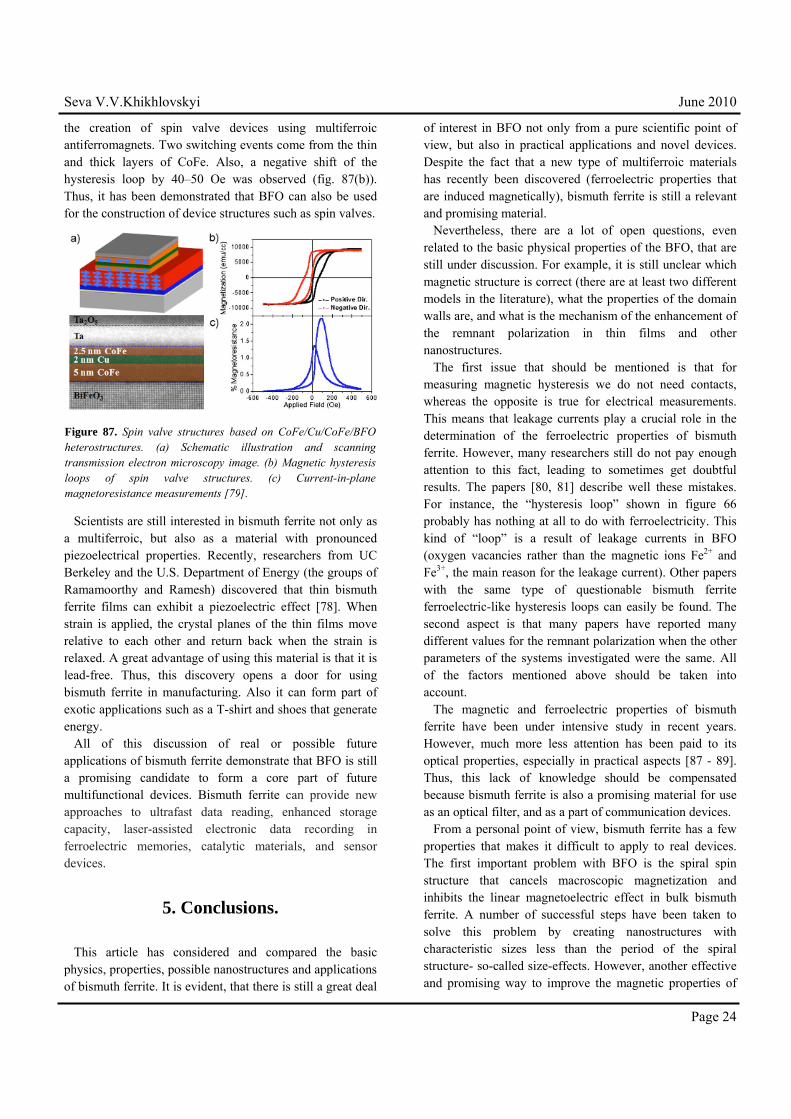
Some exciting potential applications involving BFO are magnetoelectric and spintronic applications: for example, memories that can be written using voltage and read using a magnetic field. Writing using an applied voltage has three advantages: a) it can be implemented in a solid-state circuit without mechanical parts; b) it requires little energy; c) the voltage requirements automatically scale down with thickness. For this kind of memory, the magnetic state should be electrically switchable and magnetically readable. The first condition is satisfied by BFO: an applied voltage can change the magnetic state of the sample. However, the second condition is difficult to meet because antiferromagnetic domains cannot be easily read. The use of exchange bias – magnetic interactions between ferromagnetic and antiferromagnetic neighbor layers - is an obvious solution this problem. This idea has been implemented for BiFeO3. Figure 85 describes the observation of exchange bias in thin ferromagnetic layers grown on BiFeO3, and figure 86 shows that the exchange biased ferromagnetic layer can be switched by a voltage. Thus, BiFeO3 can also be used as a barrier layer in spintronic devices. The next important issue is the possibility of creating a spin valve structure. Asymmetric spin valve structures were studied by Martin et al. [79] and consist of the following different layers: Ta, CoFe, Cu, CoFe, BFO, SRO, STO, and Si(001) (fig. 87(a)). Scanning transmission electron microscopy (STEM) was used to demonstrate the high quality nature of the heterostructure with interfaces that are very smooth and show very little interdiffusion. This allows
Figure 82. (a) THz time-domain waveforms for (100), (110), and (111) BiFeO3-oriented films. (b) Dependence of ETHz on the applied electric field generates a hysteresis loop for (100)- and (110)-oriented films and an almost linear variation with opposite polarity for (111) films [77].
Figure 83. (a) Electric-field-dependent contribution of EPs is an ideal ferroelectric-type hysteretic contribution (blue) while that of EJ (red) has a linear behavior (as in (111)-oriented films). (b) Combining the two contributions (EJ+EPs), a tilted loop results for (100) and (110) films [77].
Figure 84. Raster-scan for THz emission around a dipole-type antenna (a) recorded at zero bias after poling in an electric-field of ~200 kV cm-1 and (b) recorded at zero bias after photoassisted poling in an electric field of ~200 kV cm-1 [77].
Figure 85. Exchange-biased magnetic hysteresis loops of thin Co grown on BiFeO3. The four figures correspond to measurements along the four in-plane orientations [100], [010], [0-10], [-100] [75].
Figure 86. Electrical control of local ferromagnetism. a–c, XMCD–PEEM images taken at the Co L-edge revealing the ferromagnetic domain structure of the CoFe features in such a coplanar electrode device structure in the as-grown state (a) after the first electrical switch (b) and after the second electrical switch (c) [78].
Seva V.V.Khikhlovskyi June 2010
Page 24
the creation of spin valve devices using multiferroic antiferromagnets. Two switching events come from the thin and thick layers of CoFe. Also, a negative shift of the hysteresis loop by 40–50 Oe was observed (fig. 87(b)). Thus, it has been demonstrated that BFO can also be used for the construction of device structures such as spin valves. Scientists are still interested in bismuth ferrite not only as a multiferroic, but also as a material with pronounced piezoelectrical properties. Recently, researchers from UC Berkeley and the U.S. Department of Energy (the groups of Ramamoorthy and Ramesh) discovered that thin bismuth ferrite films can exhibit a piezoelectric effect [78]. When strain is applied, the crystal planes of the thin films move relative to each other and return back when the strain is relaxed. A great advantage of using this material is that it is lead-free. Thus, this discovery opens a door for using bismuth ferrite in manufacturing. Also it can form part of exotic applications such as a T-shirt and shoes that generate energy. All of this discussion of real or possible future applications of bismuth ferrite demonstrate that BFO is still a promising candidate to form a core part of future multifunctional devices. Bismuth ferrite can provide new approaches to ultrafast data reading, enhanced storage capacity, laser-assisted electronic data recording in ferroelectric memories, catalytic materials, and sensor devices.
5. Conclusions.
This article has considered and compared the basic physics, properties, possible nanostructures and applications of bismuth ferrite. It is evident, that there is still a great deal
of interest in BFO not only from a pure scientific point of view, but also in practical applications and novel devices. Despite the fact that a new type of multiferroic materials has recently been discovered (ferroelectric properties that are induced magnetically), bismuth ferrite is still a relevant and promising material. Nevertheless, there are a lot of open questions, even related to the basic physical properties of the BFO, that are still under discussion. For example, it is still unclear which magnetic structure is correct (there are at least two different models in the literature), what the properties of the domain walls are, and what is the mechanism of the enhancement of the remnant polarization in thin films and other nanostructures. The first issue that should be mentioned is that for measuring magnetic hysteresis we do not need contacts, whereas the opposite is true for electrical measurements. This means that leakage currents play a crucial role in the determination of the ferroelectric properties of bismuth ferrite. However, many researchers still do not pay enough attention to this fact, leading to sometimes get doubtful results. The papers [80, 81] describe well these mistakes. For instance, the “hysteresis loop” shown in figure 66 probably has nothing at all to do with ferroelectricity. This kind of “loop” is a result of leakage currents in BFO (oxygen vacancies rather than the magnetic ions Fe2+ and Fe3+, the main reason for the leakage current). Other papers with the same type of questionable bismuth ferrite ferroelectric-like hysteresis loops can easily be found. The second aspect is that many papers have reported many different values for the remnant polarization when the other parameters of the systems investigated were the same. All of the factors mentioned above should be taken into account. The magnetic and ferroelectric properties of bismuth ferrite have been under intensive study in recent years. However, much more less attention has been paid to its optical properties, especially in practical aspects [87 - 89]. Thus, this lack of knowledge should be compensated because bismuth ferrite is also a promising material for use as an optical filter, and as a part of communication devices. From a personal point of view, bismuth ferrite has a few properties that makes it difficult to apply to real devices. The first important problem with BFO is the spiral spin structure that cancels macroscopic magnetization and inhibits the linear magnetoelectric effect in bulk bismuth ferrite. A number of successful steps have been taken to solve this problem by creating nanostructures with characteristic sizes less than the period of the spiral structure- so-called size-effects. However, another effective and promising way to improve the magnetic properties of
Figure 87. Spin valve structures based on CoFe/Cu/CoFe/BFO heterostructures. (a) Schematic illustration and scanning transmission electron microscopy image. (b) Magnetic hysteresis loops of spin valve structures. (c) Current-in-plane magnetoresistance measurements [79].

Seva V.V.Khikhlovskyi June 2010
Page 25
BFO material is to perform ionic substitutions using Ca, Sr, Ba, Dy, Gd, Ce, Tb etc. Dopants might suppress the spiral spin structure and thus improve the ferromagnetic characteristics of BFO. There are many publications that report on successful improvement of the ferromagnetic properties of BFO by doping methods and by the creation of structures with an insulator-conductor transition using electrical field, that are more useful and cheaper than using a magnetic field [90]. This direction is still very interesting because it is possible to dope BFO using more than one material (dopant). The next promising idea is to use different substrates with mismatched lattice parameters with respect to BFO in order to induce epitaxial strain effects. The second problem is related to the weak magnetoelectric coupling. Possible solutions are the same as for the first problem (confinement, strain, doping effects etc). The most promising direction for practical use of BFO is in the area of memory devices. The possibility of creating an electrically controlled magnetic, non-volatile memory would be a big step forward. However, to achieve this result we should learn how to manage in a proper way the different types of domain walls in BFO (71˚, 109˚ and 180˚). A few articles have reported successfully achievement of this goal [27, 29, 30, 68], but in practice the results obtained are still insufficient to create real magnetic memory devices. From a general point of view, a most challenging problem in the field of multiferroic materials is room temperature functionality. Due to the fact that BFO successfully avoids this, it is a popular candidate to form a core part of novel nanodevices. As regards the general direction of development, one exotic possibility is to create multiferroic materials based on multiferroic-organic frameworks. Despite the fact that there have been thus far only a few papers on this subject [91, 92], I believe that these ideas have a promising future. The last interesting fact that indicates that bismuth ferrite is still a very important and promising material is that during the writing of this paper more than 25 papers concerning BFO were published. One of these studies was performed in the Zernike Institute For Advanced Materials.
6. Acknowledgements.
A special thanks goes to my supervisor Dr. Graeme Blake (Department of Chemical Physics, Zernike Institute for Advanced Materials).
7. References.
1. http://unit.aist.go.jp/ce-core/cerc/topicsE.html. 2. http://www.materials.manchester.ac.uk/. 3. W. Eerenstein, N. D. Mathur & J. F. Scott, Nature Vol.
442, 759-765 (2006). 4. L. D. Landau and E. M. Lifshitz, Electrodynamics of
continuous media (Fizmatgiz, Moscow, (1959). 5. I. E. Dzyaloshinskii, Sov. Phys. JETP 10, 628 (1959). 6. D. N. Astrov, Sov. Phys. JETP 11, 708 (1609). 7. G. A. Smolenskii and I. E. Chupis, Sov. Phys. Usp.
Vol. 25, 475 (1982). 8. T. Kimura, T. Goto, H. Shintani, K. Ishizaka, T. Arima,
Y. Tokura, Nature Vol. 426, 55-58 (2003). 9. J. R. Teague, R. Gerson and W.J. James, Sol. Stat.
Commun. 8 1073 (1970). 10. P. Fischer and M. Polomska, J. Phys. C: Sol. Stat. Vol.
13, 1931 (1980). 11. J. Wang et al., Science 299, 1719 (2003). 12. D. Khomskii, Physics 2, 20 (2009). 13. N. A. Hill, J. Phys. Chem. B 104, 6694 (2000). 14. K. Kawano, H. Kosuge, N. Oshima, H. Funakubo,
Electrochem. Sol. St. Lett. 9, C175 (2006). 15. J. F. Scott, J. Phys. Condens. Mat. Vol. 18, R361
(2006). 16. H Béa et al., J. Phys. Condens. Matter Vol. 20, 434221
(2008). 17. N. Hur et al., Nature Vol. 429, 392 (2004). 18. R. Ramesh and N. A Spaldin, Nature Mater. Vol. 6, 21
(2007). 19. M. V. Mostovoy, Phys. Rev. Lett. Vol. 96, 067601
(2006). 20. Axel Lubk, S. Gemming, and N. A. Spaldin, Phys. Rev.
B Vol. 80, 104110 (2009). 21. J. J. Jacobson and B. F. F. Fender, J. Phys. C 8, 844
(1975). 22. I. Sosnowska et al., J. Phys. C. 15, 4835 (1982). 23. A. M. Kadomtseva et al., Phase Transitions, Vol. 79,
1019-1042 (2006). 24. D. Lebeugle et al., Phys. Rev. B. 76, 024116 (2007). 25. Moriya T., Phys. Rev. 120, 91 (1960). 26. V. Raghavendra et al., Applied Physics Letters Vol. 94,
082505 (2009). 27. T. Zhao et al., Nature Mater. Vol. 5, 823 (2006). 28. Teague, Gerson and James, Solid State Commun. 8,
1073 (1963). 29. Zavaliche, et al., Appl. Phys. Lett. 87, 252902 (2005). 30. Zavaliche, et al.,. Appl. Phys. Lett. 87, 182912 (2005). 31. Lane W. Martin et al., Nano Letters Vol. 8 No. 7 2050-
2055 (2008). 32. Ying-Hao Chu et al., Adv. Mater. Vol. 19 2662-2666
(2007). 33. V.R. Palkar and R. Pinto, Pramana, Vol. 58, Nos 5 & 6,
May & June 2002, pp. 1003–1008 (2002). 34. D. Lebeugle et al., Phys. Rev. B 76, 024116 (2007). 35. Y. H. Chu et al., Appl. Phys. Let. 90, 252906 (2007).

Seva V.V.Khikhlovskyi June 2010
Page 26
36. Silvia Picozzi et al., J. Phys.: Condens. Matter Vol. 21, 303201 (2009).
37. W. Eerenstein, et al. Science Vol 307, 1203a (2005). 38. D. Lebeugle et al., Applied Physics Letters Vol 91,
022907 (2007). 39. J. B. Neaton et al., Physical Review B Vol. 71, 014113
(2005). 40. M. S. Kartavtseva et al., Thin Solid Films Vol. 518
4750–4752 (2010). 41. Palkar V R, John J and Pinto R, Appl. Phys. Lett. Vol.
80, 1628 (2002). 42. Wang J et al., Appl. Phys. Lett. 85 2574 (2003). 43. Li J et al., Appl. Phys. Lett. 84 5261 (2004). 44. Yun K Y, Noda M, Okuyama M, Saeki H, Tabata H
and Saito K, J. Appl. Phys. Vol. 96, 3399 (2004). 45. Zheng Chaodan et al., Integrated Ferroelectronics, Vol.
94, 23-30, (2007). 46. Chia-Ching Lee et al., Applied Surface Science Vol.
253 7069–7073 (2007). 47. Ho Won Jang et al., Adv. Mater. Vol. 21, 817–823
(2009). 48. R. R. Das et al., Applied Physics Letters Vol. 88,
242904 (2006). 49. T. H. Kim et al., Applied Physics Letters Vol. 95,
262902 (2009). 50. S. Y. Yang, Appl. Phys. Let. 87, 102903 (2005). 51. Risako Ueno et al., Japanese Journal of Applied
Physics, Vol. 44, No. 39, pp. L 1231–L 1233, (2005). 52. M. S. Kartavtseva et al., Journal of surface
investigation. X-ray, synchrotron and neutron techniques Vol. 2, No. 1 (2008).
53. S. Shanthy et al., Integrated Ferroelectronics, Vol. 99, 77 - 85, (2008).
54. Hongri Liu et al., Thin Solid Films Vol. 500 105 - 109 (2006).
55. Seung Wha Lee et al., Journal of Magnetism and Magnetic Materials Vol. 304, e772–e774 (2006).
56. Yao Wang et al., Applied Physics Letters Vol. 88, 142503 (2006).
57. Hongri Liu et. al., J Sol-Gel Sci Technol Vol . 47, 154–157 (2008).
58. Sushil K. Singh et al., Japanese Journal of Applied Physics Vol. 44, No. 12, pp. 8525–8527 (2005).
59. R. J. Zeches et al., Science Vol. 326, 13 (2009). 60. J. F. Ihlefeld et al., Applied Physics Letters Vol. 91,
071922 (2007). 61. J. Kabelac et al., J. Vac. Sci. Technol. B, Vol. 25, No.
3, (2007). 62. J. F. Ihlefeld et al., Applied Physics Letters Vol. 92,
142908 (2008). 63. J. F. Ihlefeld et al., IEEE International Symposium on
Applications of Ferroelectrics ISAF No17, Santa Fe, New Mexico, ETATS-UNIS (24/02/2008), Vol. 56, No. 8, pp. 1528-1533, 2009.
64. Yu-Qing Kang et al., Materials Letters Vol. 63, 1344–1346 (2009).
65. Jie Wei et al., Materials Research Bulletin Vol. 43, 3368–3373 (2008).
66. Tae-Jin Park et al., Nano Letters Vol. 7, No. 3 766-772 (2007).
67. Nandini Das et al., Materials Letters Vol. 61, 2100–2104 (2007).
68. Manoj Kumar et al., Materials Letters Vol. 62, 1159–1161 (2008).
69. Jia-Huan Xu et al., Journal of Alloys and Compounds Vol. 472, 473–477 (2009).
70. De-Chang Jia et al., Journal of the European Ceramic Society Vol. 29, 3099–3103 (2009).
71. F. Gao et al., Applied Physics Letters Vol. 89, 102506 (2006).
72. Jie Wei et al., Scripta Materialia Vol. 58, 45–48 (2008). 73. S. H. Xie et al., Applied Physics Letters Vol. 93,
222904 (2008). 74. J. Seidel et al., Nature Materials Vol. 8 (2009). 75. Gustau Catalan et al., Adv. Mater. Vol. 21, 2463–2485
(2009). 76. Hélène Béa and Patrycja Paruch, Nature materials Vol.
8 (2009). 77. Dhanvir Singh Rana et al., Adv. Mater. Vol. 21, 2881–
2885 (2009). 78. Ying-hao Chu et al., Nature materials Vol. 7 (2008). 79. Lane W. Martin et al., Applied Physics Letters Vol. 91,
172513 (2007). 80. J. F.Scott, J.Phys.: Condens. Matter Vol. 20 (2008). 81. L. Pintilie and M. Alexe, Applied Physics Letters Vol.
87 112903 (2005). 82. J. Dho, X. Qi, H. Kim, J. L. MacManus-Driscoll, and
M. G. Blamire, Adv. Mater. 18, 1445 (2006). 83. X. Qi, J. Dho, R. Tomov, M. G. Blamire, and J. L.
MacManus-Driscoll, Appl. Phys. Lett. 86, 062903 (2005).
84. C. Wang, M. Takahashi, H. Fujino, X. Zhao, E. Kume, T. Horiuchi, and S. Sakai, J. Appl. Phys. 99, 054104 (2006).
85. X. H. Xiao, J. Zhu, Y. R. Li, W. B. Luo, B. F. Xu, L. X. Fan, F. Ren, C. Liu, and C. Z. Jiang, J. Phys. D 40, 5775 (2007).
86. Y. W. Li, Z. G. Hu, F. Y. Yue, P. X. Yang, Y. N. Qian, W. J. Cheng, X. M. Ma, and J. H. Chu, J. Phys. D 41, 215403 (2008).
87. Amit Kumar et al., Applied Physics Letters Vol. 92 121915 (2008).
88. S. Iakovlev, et al., Journal of Applied Physics Vol. 92 094901 (2005).
89. Hiromi Shima et al., Japanese Journal of Applied Physics Vol. 48 09KB01 (2009).
90. C-H.Yang et al., Nature Materials Vol. 8 (2009). 91. Prashant Jain et al., Journal American Chemistry
Society Vol. 131 No. 38 (2009). 92. Guillame Rogez et al., Angew. Chem. Int. Ed. Vol. 49
1921-1923, (2010).
Related Documents