The Q/U Imaging ExperimenT (QUIET): The Q-band Receiver Array Instrument and Observations by Laura Newburgh Advisor: Professor Amber Miller Submitted in partial fulfillment of the requirements for the degree of Doctor of Philosophy in the Graduate School of Arts and Sciences COLUMBIA UNIVERSITY 2010

Welcome message from author
This document is posted to help you gain knowledge. Please leave a comment to let me know what you think about it! Share it to your friends and learn new things together.
Transcript
The Q/U Imaging ExperimenT (QUIET): TheQ-band Receiver Array Instrument and
Observations
by
Laura Newburgh
Advisor: Professor Amber Miller
Submitted in partial fulfillment of therequirements for the degree of
Doctor of Philosophy
in the Graduate School of Arts and Sciences
COLUMBIA UNIVERSITY
2010

c 2010Laura Newburgh
All Rights Reserved
Abstract
The Q/U Imaging ExperimenT (QUIET): The Q-band
Receiver Array Instrument and Observations
by
Laura Newburgh
Phase I of the Q/U Imaging ExperimenT (QUIET) measures the Cosmic Microwave
Background polarization anisotropy spectrum at angular scales 25 1000.
QUIET has deployed two independent receiver arrays. The 40-GHz array took data
between October 2008 and June 2009 in the Atacama Desert in northern Chile. The
90-GHz array was deployed in June 2009 and observations are ongoing. Both receivers
observe four 15×15 regions of the sky in the southern hemisphere that are expected
to have low or negligible levels of polarized foreground contamination. This thesis
will describe the 40 GHz (Q-band) QUIET Phase I instrument, instrument testing,
observations, analysis procedures, and preliminary power spectra.

Contents
1 Cosmology with the Cosmic Microwave Background 1
1.1 The Cosmic Microwave Background . . . . . . . . . . . . . . . . . . . 1
1.2 Inflation . . . . . . . . . . . . . . . . . . . . . . . . . . . . . . . . . . 2
1.2.1 Single Field Slow Roll Inflation . . . . . . . . . . . . . . . . . 3
1.2.2 Observables . . . . . . . . . . . . . . . . . . . . . . . . . . . . 4
1.3 CMB Anisotropies . . . . . . . . . . . . . . . . . . . . . . . . . . . . 6
1.3.1 Temperature . . . . . . . . . . . . . . . . . . . . . . . . . . . . 6
1.3.2 Polarization . . . . . . . . . . . . . . . . . . . . . . . . . . . . 7
1.3.3 Angular Power Spectrum Decomposition . . . . . . . . . . . . 8
1.4 Foregrounds . . . . . . . . . . . . . . . . . . . . . . . . . . . . . . . . 14
1.5 CMB Science with QUIET . . . . . . . . . . . . . . . . . . . . . . . . 15
2 The Q/U Imaging ExperimenT Q-band Instrument 19
2.1 QUIET Q-band Instrument Overview . . . . . . . . . . . . . . . . . . 19
2.2 Optics . . . . . . . . . . . . . . . . . . . . . . . . . . . . . . . . . . . 23
2.2.1 Introduction . . . . . . . . . . . . . . . . . . . . . . . . . . . . 23
2.2.2 Telescope Optics . . . . . . . . . . . . . . . . . . . . . . . . . 23
2.2.3 Feedhorns and Interface Plate . . . . . . . . . . . . . . . . . . 27
2.2.4 Ortho-mode Transducer Assemblies . . . . . . . . . . . . . . . 28
2.2.5 Hybrid-Tee Assembly . . . . . . . . . . . . . . . . . . . . . . . 33
2.2.6 Optics Performance . . . . . . . . . . . . . . . . . . . . . . . . 34
2.3 Polarimeter Modules . . . . . . . . . . . . . . . . . . . . . . . . . . . 49
2.3.1 Introduction . . . . . . . . . . . . . . . . . . . . . . . . . . . . 49
i
2.3.2 Polarimeter Module Components . . . . . . . . . . . . . . . . 51
2.3.3 Module Bias Optimization . . . . . . . . . . . . . . . . . . . . 60
2.3.4 Compression . . . . . . . . . . . . . . . . . . . . . . . . . . . . 61
2.3.5 Signal Processing by the QUIET Module . . . . . . . . . . . . 62
2.4 Single Module Testing at the Jet Propulsion Laboratory and Columbia
University . . . . . . . . . . . . . . . . . . . . . . . . . . . . . . . . . 77
2.5 Electronics . . . . . . . . . . . . . . . . . . . . . . . . . . . . . . . . . 79
2.5.1 Introduction . . . . . . . . . . . . . . . . . . . . . . . . . . . . 79
2.5.2 Electronics Overview . . . . . . . . . . . . . . . . . . . . . . . 80
2.5.3 Protection Circuitry . . . . . . . . . . . . . . . . . . . . . . . 84
2.5.4 Bias Boards . . . . . . . . . . . . . . . . . . . . . . . . . . . . 88
2.5.5 Monitor and Data Acquisition Boards . . . . . . . . . . . . . . 90
2.5.6 Timing cards . . . . . . . . . . . . . . . . . . . . . . . . . . . 94
2.5.7 External-Temperature Monitor Boards . . . . . . . . . . . . . 94
2.5.8 Software . . . . . . . . . . . . . . . . . . . . . . . . . . . . . . 94
2.6 Cryostat . . . . . . . . . . . . . . . . . . . . . . . . . . . . . . . . . . 96
2.6.1 Introduction . . . . . . . . . . . . . . . . . . . . . . . . . . . . 96
2.6.2 Description of W- and Q- band Cryostats . . . . . . . . . . . . 96
2.6.3 Mechanical Simulations . . . . . . . . . . . . . . . . . . . . . . 99
2.6.4 Expected and Measured Cryostat Temperatures . . . . . . . . 100
2.6.5 The Cryostat Window . . . . . . . . . . . . . . . . . . . . . . 106
3 Q-band Array Integration, Characterization, and Testing 119
3.1 Introduction . . . . . . . . . . . . . . . . . . . . . . . . . . . . . . . . 119
3.2 Bandpasses . . . . . . . . . . . . . . . . . . . . . . . . . . . . . . . . 119
3.2.1 Columbia Laboratory Data . . . . . . . . . . . . . . . . . . . . 121
3.2.2 Site Data . . . . . . . . . . . . . . . . . . . . . . . . . . . . . 122
3.2.3 Receiver Bandwidths and Central Frequencies . . . . . . . . . 124
3.2.4 Amplifier Bias . . . . . . . . . . . . . . . . . . . . . . . . . . . 128
ii
3.2.5 Central Frequencies and Bandwidths: Weighted by Source Spec-
trum . . . . . . . . . . . . . . . . . . . . . . . . . . . . . . . . 131
3.3 Noise Temperature Measurements . . . . . . . . . . . . . . . . . . . . 133
3.4 Responsivity . . . . . . . . . . . . . . . . . . . . . . . . . . . . . . . . 135
3.4.1 Total Power . . . . . . . . . . . . . . . . . . . . . . . . . . . . 135
3.4.2 Polarized Response . . . . . . . . . . . . . . . . . . . . . . . . 137
3.5 Compression . . . . . . . . . . . . . . . . . . . . . . . . . . . . . . . . 140
3.6 Noise . . . . . . . . . . . . . . . . . . . . . . . . . . . . . . . . . . . . 142
3.7 Instrument Sensitivity . . . . . . . . . . . . . . . . . . . . . . . . . . 144
4 Observations and Data Reduction 148
4.1 QUIET Observing Site . . . . . . . . . . . . . . . . . . . . . . . . . . 148
4.1.1 Observing Conditions . . . . . . . . . . . . . . . . . . . . . . . 148
4.2 Patch Selection . . . . . . . . . . . . . . . . . . . . . . . . . . . . . . 151
4.3 Scan Strategy . . . . . . . . . . . . . . . . . . . . . . . . . . . . . . . 151
4.4 Data Selection and Reduction . . . . . . . . . . . . . . . . . . . . . . 151
4.4.1 Nomenclature . . . . . . . . . . . . . . . . . . . . . . . . . . . 152
4.4.2 Standard and Static Cuts . . . . . . . . . . . . . . . . . . . . 152
4.4.3 Scan Duration . . . . . . . . . . . . . . . . . . . . . . . . . . . 153
4.4.4 Glitching Cut . . . . . . . . . . . . . . . . . . . . . . . . . . . 153
4.4.5 Phase Switch Cut . . . . . . . . . . . . . . . . . . . . . . . . . 154
4.4.6 Weather Cut . . . . . . . . . . . . . . . . . . . . . . . . . . . 155
4.4.7 Fourier-Transform Based Cuts and Filtering . . . . . . . . . . 166
4.4.8 Side-lobe Cut . . . . . . . . . . . . . . . . . . . . . . . . . . . 171
4.4.9 Coordinate System . . . . . . . . . . . . . . . . . . . . . . . . 171
4.4.10 Cut Development . . . . . . . . . . . . . . . . . . . . . . . . . 172
4.4.11 Ground Map . . . . . . . . . . . . . . . . . . . . . . . . . . . 173
4.4.12 Max-Min Removal . . . . . . . . . . . . . . . . . . . . . . . . 177
4.4.13 Source Removal and Edge-Masking . . . . . . . . . . . . . . . 179
4.4.14 Data Selected . . . . . . . . . . . . . . . . . . . . . . . . . . . 179
iii

5 Instrument Calibration and Characterization 180
5.1 Introduction . . . . . . . . . . . . . . . . . . . . . . . . . . . . . . . . 180
5.1.1 Nomenclature . . . . . . . . . . . . . . . . . . . . . . . . . . . 180
5.2 Calibration Overview . . . . . . . . . . . . . . . . . . . . . . . . . . . 181
5.2.1 Calibration Sources . . . . . . . . . . . . . . . . . . . . . . . . 181
5.3 Responsivity . . . . . . . . . . . . . . . . . . . . . . . . . . . . . . . . 183
5.3.1 Total Power Responsivity . . . . . . . . . . . . . . . . . . . . 184
5.3.2 Polarization Responsivity . . . . . . . . . . . . . . . . . . . . 185
5.3.3 Systematic Error Assessment . . . . . . . . . . . . . . . . . . 185
5.4 Sensitivity . . . . . . . . . . . . . . . . . . . . . . . . . . . . . . . . . 187
5.5 Pointing . . . . . . . . . . . . . . . . . . . . . . . . . . . . . . . . . . 188
5.5.1 Systematic Error Assessment . . . . . . . . . . . . . . . . . . 193
5.6 Timing . . . . . . . . . . . . . . . . . . . . . . . . . . . . . . . . . . . 194
5.7 Polarized Detector Angles . . . . . . . . . . . . . . . . . . . . . . . . 196
5.7.1 Systematic Error Assessment . . . . . . . . . . . . . . . . . . 198
5.8 Leakage . . . . . . . . . . . . . . . . . . . . . . . . . . . . . . . . . . 198
5.8.1 Systematic Error Assessment . . . . . . . . . . . . . . . . . . 199
5.9 Beams . . . . . . . . . . . . . . . . . . . . . . . . . . . . . . . . . . . 201
5.9.1 Polarized Beams . . . . . . . . . . . . . . . . . . . . . . . . . 201
5.9.2 Total Power Beams . . . . . . . . . . . . . . . . . . . . . . . . 204
5.9.3 Ghosting . . . . . . . . . . . . . . . . . . . . . . . . . . . . . . 205
5.9.4 Systematic Error Assessment for the Beams . . . . . . . . . . 206
5.10 Summary of Calibration and Systematics . . . . . . . . . . . . . . . . 207
5.10.1 Summary of Calibration Accuracy and Precision . . . . . . . . 207
5.10.2 Systematics Summary . . . . . . . . . . . . . . . . . . . . . . 208
6 CMB Power Spectrum Analysis and Results With a Maximum Like-
lihood Pipeline 209
6.1 Introduction . . . . . . . . . . . . . . . . . . . . . . . . . . . . . . . . 209
6.2 Maximum-Likelihood Method Background . . . . . . . . . . . . . . . 209
iv
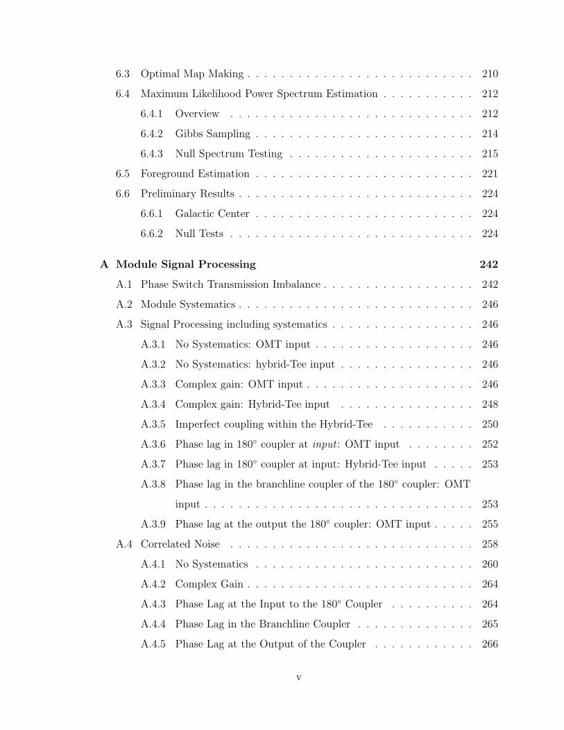
6.3 Optimal Map Making . . . . . . . . . . . . . . . . . . . . . . . . . . . 210
6.4 Maximum Likelihood Power Spectrum Estimation . . . . . . . . . . . 212
6.4.1 Overview . . . . . . . . . . . . . . . . . . . . . . . . . . . . . 212
6.4.2 Gibbs Sampling . . . . . . . . . . . . . . . . . . . . . . . . . . 214
6.4.3 Null Spectrum Testing . . . . . . . . . . . . . . . . . . . . . . 215
6.5 Foreground Estimation . . . . . . . . . . . . . . . . . . . . . . . . . . 221
6.6 Preliminary Results . . . . . . . . . . . . . . . . . . . . . . . . . . . . 224
6.6.1 Galactic Center . . . . . . . . . . . . . . . . . . . . . . . . . . 224
6.6.2 Null Tests . . . . . . . . . . . . . . . . . . . . . . . . . . . . . 224
A Module Signal Processing 242
A.1 Phase Switch Transmission Imbalance . . . . . . . . . . . . . . . . . . 242
A.2 Module Systematics . . . . . . . . . . . . . . . . . . . . . . . . . . . . 246
A.3 Signal Processing including systematics . . . . . . . . . . . . . . . . . 246
A.3.1 No Systematics: OMT input . . . . . . . . . . . . . . . . . . . 246
A.3.2 No Systematics: hybrid-Tee input . . . . . . . . . . . . . . . . 246
A.3.3 Complex gain: OMT input . . . . . . . . . . . . . . . . . . . . 246
A.3.4 Complex gain: Hybrid-Tee input . . . . . . . . . . . . . . . . 248
A.3.5 Imperfect coupling within the Hybrid-Tee . . . . . . . . . . . 250
A.3.6 Phase lag in 180 coupler at input : OMT input . . . . . . . . 252
A.3.7 Phase lag in 180 coupler at input: Hybrid-Tee input . . . . . 253
A.3.8 Phase lag in the branchline coupler of the 180 coupler: OMT
input . . . . . . . . . . . . . . . . . . . . . . . . . . . . . . . . 253
A.3.9 Phase lag at the output the 180 coupler: OMT input . . . . . 255
A.4 Correlated Noise . . . . . . . . . . . . . . . . . . . . . . . . . . . . . 258
A.4.1 No Systematics . . . . . . . . . . . . . . . . . . . . . . . . . . 260
A.4.2 Complex Gain . . . . . . . . . . . . . . . . . . . . . . . . . . . 264
A.4.3 Phase Lag at the Input to the 180 Coupler . . . . . . . . . . 264
A.4.4 Phase Lag in the Branchline Coupler . . . . . . . . . . . . . . 265
A.4.5 Phase Lag at the Output of the Coupler . . . . . . . . . . . . 266
v
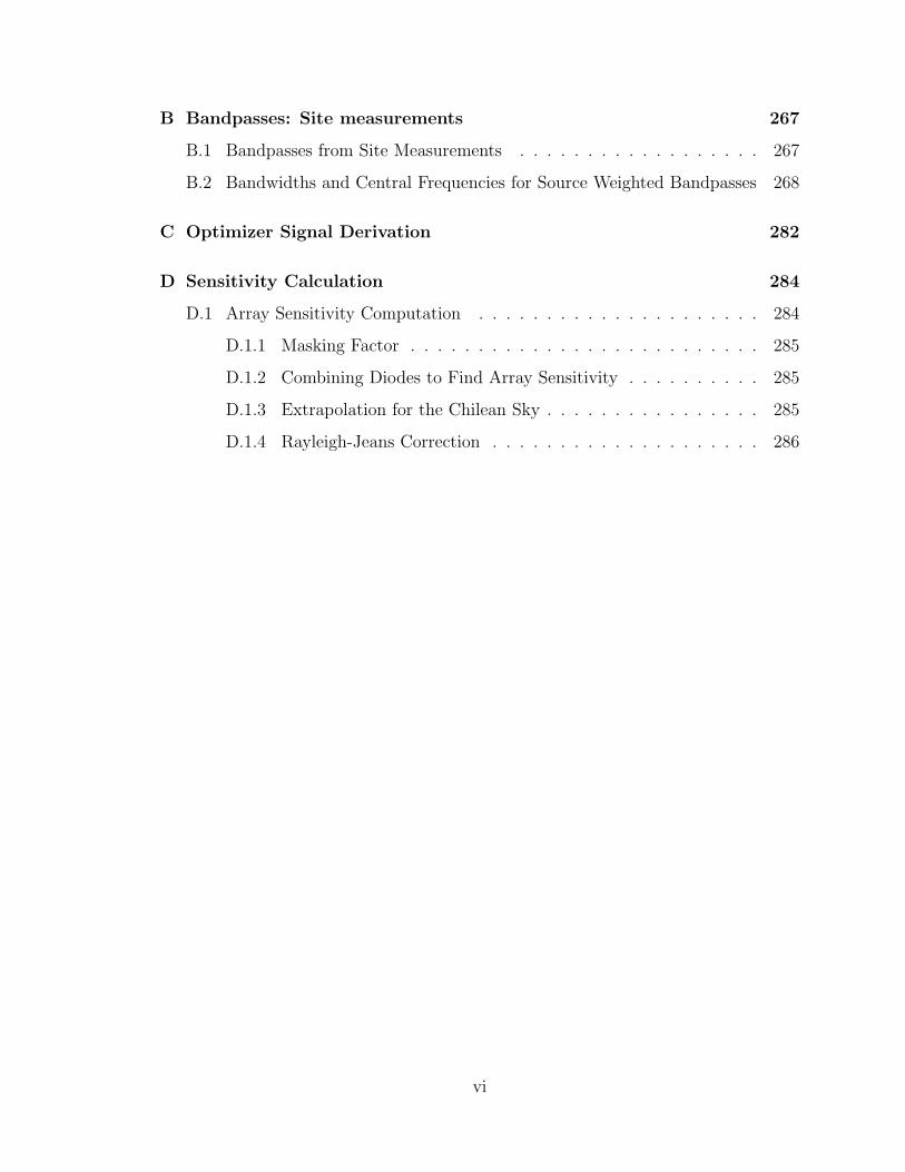
B Bandpasses: Site measurements 267
B.1 Bandpasses from Site Measurements . . . . . . . . . . . . . . . . . . 267
B.2 Bandwidths and Central Frequencies for Source Weighted Bandpasses 268
C Optimizer Signal Derivation 282
D Sensitivity Calculation 284
D.1 Array Sensitivity Computation . . . . . . . . . . . . . . . . . . . . . 284
D.1.1 Masking Factor . . . . . . . . . . . . . . . . . . . . . . . . . . 285
D.1.2 Combining Diodes to Find Array Sensitivity . . . . . . . . . . 285
D.1.3 Extrapolation for the Chilean Sky . . . . . . . . . . . . . . . . 285
D.1.4 Rayleigh-Jeans Correction . . . . . . . . . . . . . . . . . . . . 286
vi

List of Figures
1-1 Inflationary Potentials . . . . . . . . . . . . . . . . . . . . . . . . . . 3
1-2 Thomson scattering . . . . . . . . . . . . . . . . . . . . . . . . . . . . 8
1-3 Polarization around a potential well . . . . . . . . . . . . . . . . . . . 9
1-4 Polarization from a gravity wave . . . . . . . . . . . . . . . . . . . . . 10
1-5 Stokes Q and U vectors definition . . . . . . . . . . . . . . . . . . . . 11
1-6 E-mode and B-mode definition . . . . . . . . . . . . . . . . . . . . . . 12
1-7 TT, EE, and (predicted) BB anisotropy angular power spectra . . . . 13
1-8 Foreground and TT anisotropy power with frequency . . . . . . . . . 15
1-9 Foreground emission compared to CMB anisotropy signal power . . . 16
1-10 Predicted QUIET polarization angular power spectrum . . . . . . . . 18
2-1 Overview of the QUIET Instrument . . . . . . . . . . . . . . . . . . . 21
2-2 Q-band Module numbering . . . . . . . . . . . . . . . . . . . . . . . . 22
2-3 Cross-Dragone Telescope Design . . . . . . . . . . . . . . . . . . . . . 25
2-4 Q-band feedhorn array . . . . . . . . . . . . . . . . . . . . . . . . . . 28
2-5 Measured beam pattern for the Q-band horns compared to an electro-
formed horn . . . . . . . . . . . . . . . . . . . . . . . . . . . . . . . . 29
2-6 A septum polarizer OMT photograph . . . . . . . . . . . . . . . . . . 29
2-7 Septum polarizer OMT schematic . . . . . . . . . . . . . . . . . . . . 30
2-8 Schematic of the TT assembly . . . . . . . . . . . . . . . . . . . . . . 35
2-9 Simulated beam pattern for the feedhorn and mirror system . . . . . 37
2-10 Predicted ellipticity and cross-polarization for different array sizes . . 38
2-11 Sidelobe coordinate systems . . . . . . . . . . . . . . . . . . . . . . . 39
vii
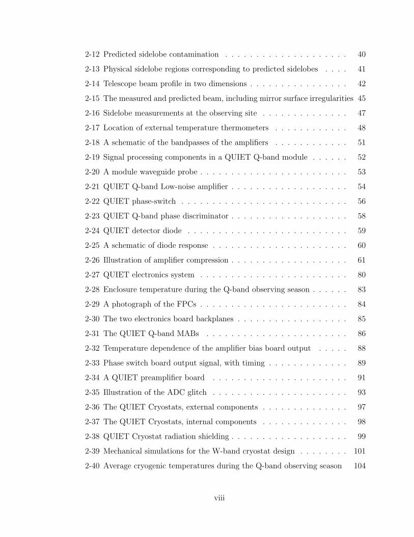
2-12 Predicted sidelobe contamination . . . . . . . . . . . . . . . . . . . . 40
2-13 Physical sidelobe regions corresponding to predicted sidelobes . . . . 41
2-14 Telescope beam profile in two dimensions . . . . . . . . . . . . . . . . 42
2-15 The measured and predicted beam, including mirror surface irregularities 45
2-16 Sidelobe measurements at the observing site . . . . . . . . . . . . . . 47
2-17 Location of external temperature thermometers . . . . . . . . . . . . 48
2-18 A schematic of the bandpasses of the amplifiers . . . . . . . . . . . . 51
2-19 Signal processing components in a QUIET Q-band module . . . . . . 52
2-20 A module waveguide probe . . . . . . . . . . . . . . . . . . . . . . . . 53
2-21 QUIET Q-band Low-noise amplifier . . . . . . . . . . . . . . . . . . . 54
2-22 QUIET phase-switch . . . . . . . . . . . . . . . . . . . . . . . . . . . 56
2-23 QUIET Q-band phase discriminator . . . . . . . . . . . . . . . . . . . 58
2-24 QUIET detector diode . . . . . . . . . . . . . . . . . . . . . . . . . . 59
2-25 A schematic of diode response . . . . . . . . . . . . . . . . . . . . . . 60
2-26 Illustration of amplifier compression . . . . . . . . . . . . . . . . . . . 61
2-27 QUIET electronics system . . . . . . . . . . . . . . . . . . . . . . . . 80
2-28 Enclosure temperature during the Q-band observing season . . . . . . 83
2-29 A photograph of the FPCs . . . . . . . . . . . . . . . . . . . . . . . . 84
2-30 The two electronics board backplanes . . . . . . . . . . . . . . . . . . 85
2-31 The QUIET Q-band MABs . . . . . . . . . . . . . . . . . . . . . . . 86
2-32 Temperature dependence of the amplifier bias board output . . . . . 88
2-33 Phase switch board output signal, with timing . . . . . . . . . . . . . 89
2-34 A QUIET preamplifier board . . . . . . . . . . . . . . . . . . . . . . 91
2-35 Illustration of the ADC glitch . . . . . . . . . . . . . . . . . . . . . . 93
2-36 The QUIET Cryostats, external components . . . . . . . . . . . . . . 97
2-37 The QUIET Cryostats, internal components . . . . . . . . . . . . . . 98
2-38 QUIET Cryostat radiation shielding . . . . . . . . . . . . . . . . . . . 99
2-39 Mechanical simulations for the W-band cryostat design . . . . . . . . 101
2-40 Average cryogenic temperatures during the Q-band observing season 104
viii
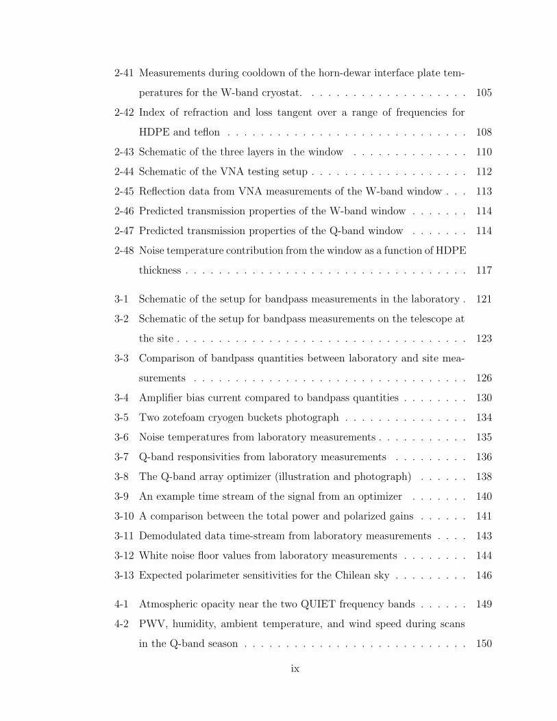
2-41 Measurements during cooldown of the horn-dewar interface plate tem-
peratures for the W-band cryostat. . . . . . . . . . . . . . . . . . . . 105
2-42 Index of refraction and loss tangent over a range of frequencies for
HDPE and teflon . . . . . . . . . . . . . . . . . . . . . . . . . . . . . 108
2-43 Schematic of the three layers in the window . . . . . . . . . . . . . . 110
2-44 Schematic of the VNA testing setup . . . . . . . . . . . . . . . . . . . 112
2-45 Reflection data from VNA measurements of the W-band window . . . 113
2-46 Predicted transmission properties of the W-band window . . . . . . . 114
2-47 Predicted transmission properties of the Q-band window . . . . . . . 114
2-48 Noise temperature contribution from the window as a function of HDPE
thickness . . . . . . . . . . . . . . . . . . . . . . . . . . . . . . . . . . 117
3-1 Schematic of the setup for bandpass measurements in the laboratory . 121
3-2 Schematic of the setup for bandpass measurements on the telescope at
the site . . . . . . . . . . . . . . . . . . . . . . . . . . . . . . . . . . . 123
3-3 Comparison of bandpass quantities between laboratory and site mea-
surements . . . . . . . . . . . . . . . . . . . . . . . . . . . . . . . . . 126
3-4 Amplifier bias current compared to bandpass quantities . . . . . . . . 130
3-5 Two zotefoam cryogen buckets photograph . . . . . . . . . . . . . . . 134
3-6 Noise temperatures from laboratory measurements . . . . . . . . . . . 135
3-7 Q-band responsivities from laboratory measurements . . . . . . . . . 136
3-8 The Q-band array optimizer (illustration and photograph) . . . . . . 138
3-9 An example time stream of the signal from an optimizer . . . . . . . 140
3-10 A comparison between the total power and polarized gains . . . . . . 141
3-11 Demodulated data time-stream from laboratory measurements . . . . 143
3-12 White noise floor values from laboratory measurements . . . . . . . . 144
3-13 Expected polarimeter sensitivities for the Chilean sky . . . . . . . . . 146
4-1 Atmospheric opacity near the two QUIET frequency bands . . . . . . 149
4-2 PWV, humidity, ambient temperature, and wind speed during scans
in the Q-band season . . . . . . . . . . . . . . . . . . . . . . . . . . . 150
ix
4-3 QUIET sky patches . . . . . . . . . . . . . . . . . . . . . . . . . . . . 156
4-4 Illustration of de-glitching . . . . . . . . . . . . . . . . . . . . . . . . 157
4-5 Phase switch bias current data cut . . . . . . . . . . . . . . . . . . . 158
4-6 Weather data cut criteria . . . . . . . . . . . . . . . . . . . . . . . . . 159
4-7 Example time-streams for determining the weather data cut . . . . . 162
4-8 Example standard deviation of time-streams for determining the weather
data cut . . . . . . . . . . . . . . . . . . . . . . . . . . . . . . . . . . 163
4-9 The weather cut compared to diode I→Qleakage . . . . . . . . . . . . 165
4-10 Example FFT of a demodulated time stream . . . . . . . . . . . . . . 168
4-11 Distribution of χ2 to the FFT noise model . . . . . . . . . . . . . . . 170
4-12 A co-added map for all CESes in a flat projection of the sun-boresight
coordinates for RQ02 . . . . . . . . . . . . . . . . . . . . . . . . . . . 173
4-13 A ground map . . . . . . . . . . . . . . . . . . . . . . . . . . . . . . . 175
4-14 A ground map . . . . . . . . . . . . . . . . . . . . . . . . . . . . . . . 176
4-15 An example of a TOD spike . . . . . . . . . . . . . . . . . . . . . . . 177
4-16 Distribution of extreme TOD outliers . . . . . . . . . . . . . . . . . . 178
5-1 Array sensitivity for the polarization modules . . . . . . . . . . . . . 188
5-2 Illustration of the collimation offset parameters . . . . . . . . . . . . 191
5-3 Deck encoder slip through the observing season . . . . . . . . . . . . 193
5-4 Illustration of the timing offset measurements . . . . . . . . . . . . . 195
5-5 Timing offset correction . . . . . . . . . . . . . . . . . . . . . . . . . 196
5-6 A comparison of detector angles . . . . . . . . . . . . . . . . . . . . . 197
5-7 A comparison of I→Qleakage coefficients . . . . . . . . . . . . . . . . 200
5-8 Normalized maps of Tau A for the central polarimeter . . . . . . . . . 202
5-9 Radial beam profile for the central polarimeter . . . . . . . . . . . . . 203
5-10 Window function for the polarization modules . . . . . . . . . . . . . 204
5-11 Window function for the hybrid-Tee modules . . . . . . . . . . . . . . 205
5-12 Map of the moon and ghosted moon in RQ04 . . . . . . . . . . . . . 206
6-1 A schematic of a two-variable posterior . . . . . . . . . . . . . . . . . 214
x
6-2 Illustration of quantifying consistency with null for power spectrum
null-tests . . . . . . . . . . . . . . . . . . . . . . . . . . . . . . . . . . 223
6-3 Galactic Center polarized maps . . . . . . . . . . . . . . . . . . . . . 225
6-4 Null map of the ‘pointside’ null test . . . . . . . . . . . . . . . . . . . 226
6-5 The angular power spectrum for the ‘pointside’ null test . . . . . . . 227
6-6 P-test for the ‘pointside’ null test . . . . . . . . . . . . . . . . . . . . 228
B-1 Q1 diode bandpasses measured by site data . . . . . . . . . . . . . . 268
B-2 Q2 diode bandpasses measured by site data . . . . . . . . . . . . . . 269
B-3 Q1 diode bandpasses . . . . . . . . . . . . . . . . . . . . . . . . . . . 270
B-4 Q2 diode bandpasses . . . . . . . . . . . . . . . . . . . . . . . . . . . 271
xi

List of Tables
2.1 QUIET Phase I instrument and observations overview . . . . . . . . . 20
2.2 Parameters for the QUIET mirror design . . . . . . . . . . . . . . . . 24
2.3 Simulated Q-band beam characteristics . . . . . . . . . . . . . . . . . 36
2.4 Compression points of the low-noise amplifiers . . . . . . . . . . . . . 63
2.5 Module systematics and resulting demodulated and averaged signal . 73
2.6 Summary of correlation coefficients . . . . . . . . . . . . . . . . . . . 76
2.7 Summary of electronics boards for the Q- and W-band polarimeter arrays 81
2.8 Dimensions of the external elements of each cryostat . . . . . . . . . 100
2.9 Calculated thermal loading from various sources with 300K and 270K
environment temperature . . . . . . . . . . . . . . . . . . . . . . . . . 102
2.10 Refrigerator temperatures given loading for the W- and Q-band receivers103
2.11 Average cryogenic temperatures during the Q-band observing season 103
2.12 Calculated and Measured thermal gradient between modules . . . . . 106
2.13 Window Testing Results . . . . . . . . . . . . . . . . . . . . . . . . . 107
2.14 Window material thicknesses and indices of refraction . . . . . . . . . 113
2.15 Predicted transmission properties of each window . . . . . . . . . . . 114
2.16 Noise temperature contribution for the W-band and Q-band windows 118
3.1 Q-band polarimeter array central frequencies . . . . . . . . . . . . . . 127
3.2 Q-band polarimeter array bandwidths . . . . . . . . . . . . . . . . . . 128
3.3 Q-band hybrid-Tee central frequencies . . . . . . . . . . . . . . . . . 129
3.4 Q-band hybrid-Tee bandwidths . . . . . . . . . . . . . . . . . . . . . 129
3.5 Spectral indices at Q-band for various sources . . . . . . . . . . . . . 132
xii
3.6 Expected polarized emission from the optimizer . . . . . . . . . . . . 139
4.1 Description of static and standard data cuts . . . . . . . . . . . . . . 153
4.2 Weather variable standard deviation criteria for two example time
streams . . . . . . . . . . . . . . . . . . . . . . . . . . . . . . . . . . 161
4.3 Percentage of data cut by each data cut . . . . . . . . . . . . . . . . 179
5.1 QUIET calibration scheme . . . . . . . . . . . . . . . . . . . . . . . . 183
5.2 Responsivity model systematic errors . . . . . . . . . . . . . . . . . . 187
5.3 Beam parameters from calibration observations . . . . . . . . . . . . 202
5.4 Preliminary calibration precision for QUIET Phase I . . . . . . . . . 207
5.5 Maximum systematic errors, expressed as a percentage of the statistical
error . . . . . . . . . . . . . . . . . . . . . . . . . . . . . . . . . . . . 208
6.1 Maximum Likelihood null tests . . . . . . . . . . . . . . . . . . . . . 217
6.2 Summary of patch foreground contamination . . . . . . . . . . . . . . 221
6.3 Summary of expected patch foreground contamination . . . . . . . . 222
B.1 Q-band array central frequencies for dust foreground. . . . . . . . . . 272
B.2 Q-band array bandwidths for dust emission . . . . . . . . . . . . . . . 273
B.3 Q-band array central frequencies for sychrotron emission . . . . . . . 274
B.4 Q-band array bandwidths for sychrotron emission . . . . . . . . . . . 275
B.5 Q-band array central frequencies for Tau A . . . . . . . . . . . . . . . 276
B.6 Q-band array bandwidths for Tau A . . . . . . . . . . . . . . . . . . 277
B.7 Q-band array bandwidths for 250mm PWV . . . . . . . . . . . . . . 278
B.8 Q-band array central frequencies for 250mm PWV . . . . . . . . . . . 279
B.9 Q-band array bandwidths for 5000mm PWV . . . . . . . . . . . . . . 280
B.10 Q-band array central frequencies for 5000mm PWV . . . . . . . . . . 281
xiii

Acknowledgments
Thanks first to my advisor and mentor, Amber Miller. You have been generous with
your time, have always had your door open, have demanded the best, but always
given room to make mistakes.
I have been extremely fortunate to have worked in the Miller lab and be surrounded
by smart, knowledgeable, amazing, fun people. I can’t possibly list everything I’ve
learned from you all, so I won’t try, and instead just say: Ross, thanks for never
letting me off the hook and making each day a bit of an adventure. Rob, you keep me
laughing even when its (likely) at myself. Jonathan, thanks for leading me through
the harrowing world of Baysian analysis and only making fun of me a fraction of the
time you could have. Seth, thank you for always being willing to help, whether it was
welding cold-straps or extracting our data. And thank you Michele, because I always
have just one last question.
Working on QUIET was an incredible learning experience, for which I would like
to thank the entire QUIET collaboration, with a special thanks to our PI, Bruce
Winstein. Thanks also to the Q-band deployment team for making the Caltech high-
bay and Chilean desert an unforgettable experience: Simon, Michele, Ross, Rob, Ali,
Immanuel, Raul, Ricardo, Rodrigo, Cristobal, and Jose. If I have more pictures of
flamingos in Chile than the Q-band cryostat, its your fault.
Thank you Mom and Dad because you never once said girls can’t do science, and
thank you Kate and Maggie, for being awesome, supportive sisters. Thank you Tanya
and Malika, for keeping me sane since college. Thank you Mari for keeping me young
at heart, and Azfar, whose unconditional support was a great gift.
xiv
Chapter 1
Cosmology with the Cosmic
Microwave Background
Today, a variety of different data sets have converged to a common model describing
the Universe and its constituents: it is expanding at an accelerated rate and its
energy density is dominated by dark energy, with smaller contributions from cold
dark matter, baryonic matter, photons, and neutrinos. Measurements of the Cosmic
Microwave Background (CMB) played a critical role in forming this model. This
chapter will discuss the origin of the CMB and how we can use measurements of the
CMB to constrain models describing the dynamics of the Universe when it was less
than 10−30 seconds old.
1.1 The Cosmic Microwave Background
When the Universe was not yet 380,000 years old, photons, baryons, and electrons
were tightly coupled, forming a photon-baryon fluid. As the universe expanded and
cooled to a temperature of 1/4 eV, the electrons began to bind to protons to form
neutral elements, predominantly hydrogen, and the scattering cross section for pho-
tons off of electrons dropped dramatically. As a result, the photons were decoupled
from the electrons and the CMB was formed by free photons at the surface of last
scattering, this era is known as decoupling or recombination. The CMB was emitted
1
2
from a uniform, hot plasma such that at decoupling it had a black-body spectrum
with a wavelength peak 1µm (infrared band). As the universe continued to expand
and cool, the wavelength of this background radiation stretched such that today
it lies in the microwave band and has a Planck spectrum peak at 2.726K±0.01K
(Ref. [65]). Today we know the temperature of this surface is uniform to one part in
105 (Refs. [66],[33],[87],[46],[79],[51]).
1.2 Inflation
There are a variety of theories that describe the dynamics of the early universe, none
of which are experimentally proven. We will limit ourselves to briefly describing the
best-motivated class of these: inflation. Inflation describes a period in which the
Universe underwent brief, exponential expansion (Ref. [32],[61]), increasing in size
by 25 orders of magnitude in 10−34 seconds when it was 10−30 seconds old
(Ref. [4]). Inflation naturally explains three observations (Ref. [59]):
1. Lack of Observed Relic Particles: A variety of stable particles such as
magnetic monopoles should be created when symmetry was broken in the early
Universe at energies 1016 GeV, however these particles have not been ob-
served. Inflation dilutes their abundance such that they would be too rare to
observe today (Ref. [50]).
2. Super-horizon Fluctuations: The uniformity of the CMB shows that scales
which were causally disconnected during recombination had been in thermal
equilibrium. This homogeneity arises naturally from inflationary theory; those
regions were causally connected before they were pushed apart by inflationary
expansion.
3. Flatness: Observations show the universe is very close to spatially flat (Ref. [66]).
This is a natural prediction of inflation as it dilutes the curvature of space in
3
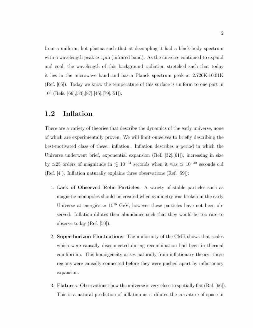
(a) (b)
Figure 1-1: Figures from Ref. [4]. An example slow-roll potential V (φ) for a: smallfield φ and b: large field φ inflationary models. The conditions for small and large fieldmodels are discussed in the text. The fluctuations seen in the CMB were imprintedat φCMB and blown to large scales during inflation. Reheating refers to the processby which the inflaton decayed to form standard model particles.
much the same way that it dilutes the relic particles.
1.2.1 Single Field Slow Roll Inflation
Inflationary expansion is sourced by the motion of one or more primordial field/s in
a potential. While there are a variety of inflationary models, here we consider only
the simplest class: single scalar-field slow-roll inflationary models. Slow-roll inflation
requires that the potential is not particularly steep, this condition will provide a
natural mechanism for generating the expansion rate necessary for inflation to solve
the three problems presented above. Examples of two typical potentials which could
give rise to slow-roll inflationary expansion are shown in Figures 1-1(a) and 1-1(b).
The slow-roll condition will place constraints on the kinetic terms of the equations of
motion (Ref. [60]), which are parametrized by and η (the ‘slow-roll parameters’):
4
= −H
H=
M2
pl
2
φ2
H2≈
M2
pl
2
V
V
2
1 (1.1)
|η| = M2
pl
V
V
1 (1.2)
where () denotes a derivative with respect to φ. The end-point of inflation is model-
dependent but will occur when the slow-roll condition is violated: → 1.
1.2.2 Observables
Inflationary models generally predict perturbations in the inflaton field δφ(t,x) and
in the metric δgµν(t,x) prior to inflation. These perturbations can be transformed
to Fourier space (δφ(t,x) → δφ(k) and δgµν(t,x) → δgµν(k)) and then decomposed
into scalar and tensor perturbations1. Computing the two-point correlation of the
scalar perturbations will yield a power spectrum of scalar fluctuations, Ps, given by
equation 1.3:
Ps(k) = As(k∗)
k
k∗
ns(k∗)−1+12αs(k∗)ln(k/k∗)
(1.3)
that is dependent on a normalization As, a spectral tilt ns, and a parameter αs, which
gives the slope of the spectral tilt with scale. All are defined at a specific scale k∗,
known as the pivot scale (Ref. [4]). ns = 1 would give a scale-invariant spectrum of
scalar perturbations, such that the distribution of power is uniform over all scales.
The two-point correlation of tensor perturbations yield a power spectrum of tensor
1Vector perturbations are also included in this decomposition, but non-negligible amplitudes ofthese perturbations are unique to predictions from specific models that we are not considering here.
5
perturbations, Pt, given by 1.4 (Ref. [92], form taken from Ref. [4]):
Pt(k) = At(k∗)
k
k∗
nt(k∗)
(1.4)
with amplitude At and spectral tilt parameter nt. nt = 0 would give a scale-invariant
spectrum of tensor perturbations. The tensor perturbations represent gravitational
wave generation, sourcing primordial inflationary gravity waves.
The tensor-to-scalar ratio, rk = Ps(k)
Pt(k), describes the relative amplitude of the scalar
and tensor fluctuations at the end of inflation. For slow-roll inflation, the spectral
tilts are directly related to the slow-roll parameters as ns− 1 = 2η− 6 and nt = −2
(Ref. [60]). In these models, the tensor-to-scalar ratio r determines the energy scale
of inflation as (Ref. [3]):
V1/4 = 1.06× 10¹⁶GeV
r∗
0.01
1/4
(1.5)
where r∗ denotes the tensor-to-scalar ratio when perturbations currently seen in the
CMB were imprinted (denoted by φCMB in Figures 1-1(a) and 1-1(b)). Consequently
r can be used to distinguish between different models with unique predictions of the
energy scale of inflation. A class of inflationary models known as ‘large-field’ models
are characterized by a relatively large tensor-to-scalar ratio, expressed in relation to
the Planck mass:
∆φ
Mpl
1.06×
r∗
0.01
1/2
(1.6)
An example of a large-field potential is given in Figure 1-1(b). A detection of r∗ 0.01
would yield an energy scale of inflation near the Grand Unified Theory (GUT) scale
and shed light on physics at the highest energies, inaccessible to particle accelerators.
If r∗ < 0.01, an entire class of inflationary models would be ruled out and small-field
6
inflationary models or non-inflationary models would be favored (an example of a
small-field potential is given in Figure 1-1(a)). The current lower bound on r is 0.22
(Ref. [51]) and the goal of QUIET Phase II (for which the work in this thesis is a
pathfinder experiment) is to probe values of r 0.01.
1.3 CMB Anisotropies
1.3.1 Temperature
Scalar perturbations give rise to over- and under-dense regions which will leave an
imprint in the CMB during decoupling. Over-dense regions represent potential wells
which will aggregate matter over time through gravitational collapse. Together, the
over- and under-dense regions source the large scale structure in the Universe.
Prior to decoupling, photons and baryons were tightly coupled. In the presence
of a potential well, the photons and baryons form an oscillatory system in which the
driving forces are gravitational collapse and photon pressure. The temperature of the
photon-baryon fluid near the potential well from a given oscillatory mode is expressed
as a fraction of the average temperature (∆TT ) and is a combination of the depth of
the potential well Ψ and the baryon density (expressed as a fraction of the average
density: δρρ ), as (Ref. [23]):
∆T
T−Ψ ∝ −
δρ
ρ
(1.7)
Equation 1.7 shows that a compressive mode ( δρρ > 0) has a temperature which is
lower than the background temperature, while the opposite is true for the rarefied
mode ( δρρ < 0). This is caused by the Sachs-Wolfe effect: although over-dense regions
are hotter, the dominant effect results from the fact that photons must climb out
of a larger potential during compression and hence are red-shifted, while photons in
7
the rarified state will be blue-shifted. These temperature fluctuations are imprinted
on the CMB, creating cold regions where an oscillatory mode was at a maximum of
its compression and hot regions at the rarified maximum. The resulting temperature
anisotropies in the CMB encode these ”acoustic spectra” formed from scalar pertur-
bations. These acoustic spectrum can be seen in Figure 1-7 as the the periodic peaks
(ΘΘ in the figure). The low- portion of the spectrum ( < 100) represent modes
which were too large to have been in causal contact at decoupling. The first peak
at 200 represents the first mode, which had just compressed at decoupling, the
second peak had just had time to compress and rarify, and so on.
1.3.2 Polarization
Polarization in the CMB is generated when radiation incident on a free electron has
a quadrupole moment, as shown in Figure 1-2. This quadrupole pattern is produced
primarily by acceleration of the photon-baryon fluid. This fluid flow can be sourced
both by potential wells or by the gravity waves generated by tensor perturbations
during inflation.
The oscillatory modes discussed in Section 1.3.1 accelerate the photon-baryon
fluid. As shown in Figure 1-3, as the photon-baryon fluid falls into a potential well,
the photons emitted from that region will appear blue-shifted in the rest-frame of a
falling electron. This produces a quadrupole temperature anisotropy and results in
polarization which is radial around the potential well. Polarization generated while
the oscillatory mode is rarifying will have a tangential pattern (see Ref. [41] for a
review, [51] for evidence of this from WMAP data).
Gravity waves generated during inflation will stretch and compress space as they
propagate. As shown in Figure 1-4, this will create red-shifted photons where space
is stretched in the rest-frame of a stationary electron in the middle of this distor-
tion, and blue-shifted photons from areas where space is compressed. This generates
a quadrupole temperature pattern and hence polarization via Thomson scattering
8
Figure 1-2: Figure adapted from Ref [41], courtesy Britt Reichborn-Kjennerud(Ref. [75]). Thomson scattering of CMB photons off of an electron located in aquadrupole radiation field. As discussed in the text, a quadrupole radiation fieldis sourced by cold spots from regions which are red-shifted, and hot spots from re-gions which are blue-shifted, due to bulk fluid flow. The scattered radiation from theblue-shifted region to the observer will be polarized vertically since the componentalong the line-of-sight will not be seen, while the scattered light from the red-shiftedregion will be polarized horizontally. The intensity of the scattered light from theblue-shifted region is greater than that of the red-shifted region, this produces overalllinear polarization.
(Figure 1-2).
1.3.3 Angular Power Spectrum Decomposition
We can write polarization in the basis of the Stokes vectors I, Q, U , and V . The
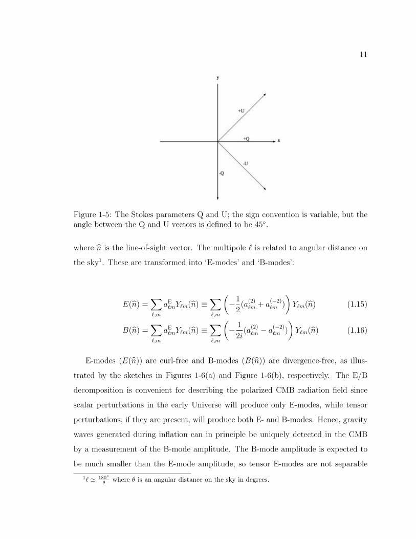
coordinate system is shown in Figure 1-5, and the vectors are defined as:
E = xExeik·x−ωt + yEye
ik·y−ωt (1.8)
I = E2
x + E2
y (1.9)
Q = E2
x − E2
y (1.10)
U = ExEy cos θ (1.11)
V = ExEy sin(θ) (1.12)
9
Figure 1-3: Top: An electron falling into a potential well (the length of the linesdenote the magnitude of acceleration). Middle: In the rest frame of the electron,the plasma nearer to the potential well and also further away from the potentialwell is accelerating away, and so the light appears red-shifted. Lower: As a result,the electron will see a quadrupole temperature pattern, which generates polarizationvia Thomson scattering (Figure 1-2). In this case, the resulting polarization will behorizontal, and will form a radial polarization pattern around the potential well.
10
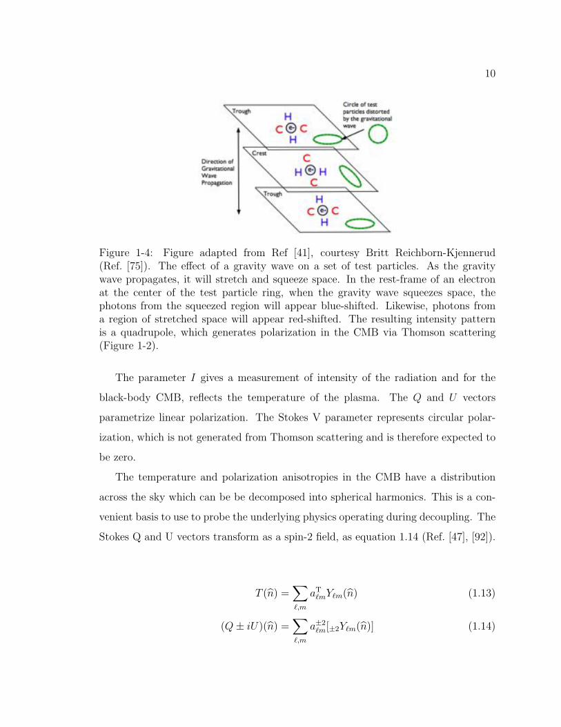
Figure 1-4: Figure adapted from Ref [41], courtesy Britt Reichborn-Kjennerud(Ref. [75]). The effect of a gravity wave on a set of test particles. As the gravitywave propagates, it will stretch and squeeze space. In the rest-frame of an electronat the center of the test particle ring, when the gravity wave squeezes space, thephotons from the squeezed region will appear blue-shifted. Likewise, photons froma region of stretched space will appear red-shifted. The resulting intensity patternis a quadrupole, which generates polarization in the CMB via Thomson scattering(Figure 1-2).
The parameter I gives a measurement of intensity of the radiation and for the
black-body CMB, reflects the temperature of the plasma. The Q and U vectors
parametrize linear polarization. The Stokes V parameter represents circular polar-
ization, which is not generated from Thomson scattering and is therefore expected to
be zero.
The temperature and polarization anisotropies in the CMB have a distribution
across the sky which can be be decomposed into spherical harmonics. This is a con-
venient basis to use to probe the underlying physics operating during decoupling. The
Stokes Q and U vectors transform as a spin-2 field, as equation 1.14 (Ref. [47], [92]).
T (n) =
,m
aT
mYm(n) (1.13)
(Q ± iU)(n) =
,m
a±2
m[±2Ym(n)] (1.14)
11
Figure 1-5: The Stokes parameters Q and U; the sign convention is variable, but theangle between the Q and U vectors is defined to be 45.
where n is the line-of-sight vector. The multipole is related to angular distance on
the sky1. These are transformed into ‘E-modes’ and ‘B-modes’:
E(n) =
,m
aE
mYm(n) ≡
,m
−
1
2(a(2)
m + a(−2)
m )
Ym(n) (1.15)
B(n) =
,m
aE
mYm(n) ≡
,m
−
1
2i(a(2)
m − a(−2)
m )
Ym(n) (1.16)
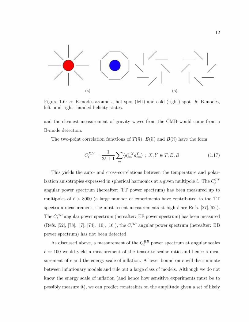
E-modes (E(n)) are curl-free and B-modes (B(n)) are divergence-free, as illus-
trated by the sketches in Figures 1-6(a) and Figure 1-6(b), respectively. The E/B
decomposition is convenient for describing the polarized CMB radiation field since
scalar perturbations in the early Universe will produce only E-modes, while tensor
perturbations, if they are present, will produce both E- and B-modes. Hence, gravity
waves generated during inflation can in principle be uniquely detected in the CMB
by a measurement of the B-mode amplitude. The B-mode amplitude is expected to
be much smaller than the E-mode amplitude, so tensor E-modes are not separable
1 180
θ where θ is an angular distance on the sky in degrees.
12
(a) (b)
Figure 1-6: a: E-modes around a hot spot (left) and cold (right) spot. b: B-modes,left- and right- handed helicity states.
and the cleanest measurement of gravity waves from the CMB would come from a
B-mode detection.
The two-point correlation functions of T (n), E(n) and B(n) have the form:
CX,Y =
1
2 + 1
m
a∗ Xm a
Ym ; X,Y ∈ T, E,B (1.17)
This yields the auto- and cross-correlations between the temperature and polar-
ization anisotropies expressed in spherical harmonics at a given multipole . The CTT
angular power spectrum (hereafter: TT power spectrum) has been measured up to
multipoles of > 8000 (a large number of experiments have contributed to the TT
spectrum measurement, the most recent measurements at high- are Refs. [27],[62]).
The CEE angular power spectrum (hereafter: EE power spectrum) has been measured
(Refs. [52], [78], [7], [74], [10], [16]), the CBB angular power spectrum (hereafter: BB
power spectrum) has not been detected.
As discussed above, a measurement of the CBB power spectrum at angular scales
100 would yield a measurement of the tensor-to-scalar ratio and hence a mea-
surement of r and the energy scale of inflation. A lower bound on r will discriminate
between inflationary models and rule out a large class of models. Although we do not
know the energy scale of inflation (and hence how sensitive experiments must be to
possibly measure it), we can predict constraints on the amplitude given a set of likely
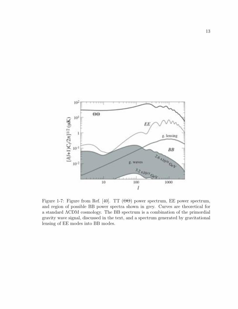
13
Figure 1-7: Figure from Ref. [40]. TT (ΘΘ) power spectrum, EE power spectrum,and region of possible BB power spectra shown in grey. Curves are theoretical fora standard ΛCDM cosmology. The BB spectrum is a combination of the primordialgravity wave signal, discussed in the text, and a spectrum generated by gravitationallensing of EE modes into BB modes.
14
inflationary models; these are shown in Figure 1-7. These models represent a partic-
ular case of compelling models, all of which would be ruled out by a non-detection of
B-modes. This also shows the relative amplitudes of the TT (ΘΘ) and EE spectrum.
As the CMB photons traverse space, they can be scattered by local gravitational
potentials (e.g. clusters, superclusters) which introduces leakage between the EE
spectrum and BB spectrum on scales commensurate with large-scale structure angu-
lar sizes. The resulting BB spectrum is shown in Figure 1-7 peaking at small scales
(labeled ‘g.lensing’). The BB spectrum from lensing is expected regardless of cos-
mological model given the measured EE spectrum and measurements of large-scale
structure. Thus, the lensed spectrum can be used to probe the evolution of struc-
ture and possibly the expansion history of the Universe (Refs. [93], [37], for a review
see [81]) and also represents a way to verify measurement and analysis techniques
to demonstrate our ability to differentiate between the EE spectrum from the BB
spectrum from a cosmological signal.
1.4 Foregrounds
The primary known sources of foreground contamination to the polarized CMB signal
are synchrotron and dust emission. The spectral dependence of each foreground
source is shown in Figure 1-8: sychrotron emission is the dominant foreground at
lower frequencies, while dust dominates the foreground emission at higher frequencies.
Many current CMB polarization experiments observe regions of the sky which have
been measured to have low foreground emission in temperature (we do not yet have
sensitive enough measurements of the polarized foregrounds so we need to extrapolate
the expected signal from the temperature emission). As seen in Figure 1-9(b) the
EE spectrum can be measured from clean patches of sky without careful attention
to foreground subtraction, however measuring the B-mode signal (Figure 1-9(c) for
r ∼0.01) will possibly require measurement and cleaning of foreground emission. Most
15
Figure 1-8: Figure from NASA/WMAP Science Team (Ref. [6]). Frequency depen-dence and amplitude of foreground emission. The CMB TT anisotropy power levelis shown in comparison. The magnitude of the polarization anisotropy spectrum willbe lower, and free-free emission is not strongly polarized.
current CMB polarization experiments have chosen to observe at multiple frequencies
to measure the slope of the foreground emission dominant at their observing frequency
to separate it from the signal.
1.5 CMB Science with QUIET
QUIET observes at 40 and 90 GHz (Q- and W-band). The QUIET Phase I Q-band
array is the subject of this thesis. The Q- and W-band arrays comprise a pathfinder
experiment for QUIET Phase II. The QUIET Phase I science goals include:
• Measure the first three peaks of the EE power spectrum σ.
• Place a competitive upper limit on the BB power spectrum, both the primordial
and lensed signals.
• Measure or place upper limits on the amplitude of polarized synchrotron emis-
sion in the cleanest regions of the sky (we selected low-foreground-emission sky
regions for observations).
16
(a) (b)
(c)
Figure 1-9: Figure from Ref. [25]. The ratio of foreground emission to CMB signal for:a: TT, b: EE, and c: BB power spectra at of 80-120 (where the primordial spectrumis predicted to peak) for various sky cuts. The lower frequency foreground contami-nation is dominated by synchrotron emission, while the higher frequency foregroundsare dominated by dust (as shown in Figure 1-8). The magnitude of the dust emissionassumes a polarization fraction of 1-2%. The amplitude used for the BB spectra iscomputed assuming r=0.01. The black line shows the ratio for the full sky, in thiscase all CMB anisotropy power spectra are dominated by foregrounds. The greenline shows the ratio for the WMAP sky-cut template known as KP2, for this casethe emission is lower than the TT and EE anisotropy power, but dominates the BBspectrum. The same is true for sky regions including only galactic latitudes greaterthan |30| (red line) and galactic latitudes greater than 50 (blue line). The mostconservative sky cut, a 10 patch of sky centered around the ‘southern hole’ a regionof minimal dust contamination, is the only region of sky in which the primordial BBpower might dominate the foreground emission.
17
• Serve as a demonstration of technology and techniques for the larger QUIET
Phase II experiment.
The Q-band data set is complete and the W-band measurements are underway,
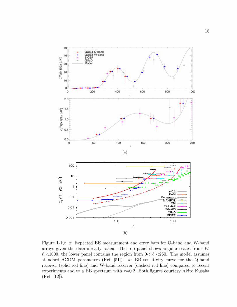
the expected bounds on the EE spectrum and BB spectrum are shown in Figures 1-
10(a) and 1-10(b). The Q-band channel was designed as a foreground monitor, the
BB spectrum from this receiver will not place a competitive bound on the amplitude
of the BB power spectrum and resulting tensor-to-scalar ratio. The W-band channel
with the data currently taken will place competitive bounds on the BB amplitude, and
will measure the third peak of the EE spectrum with greater precision than current
experimental results.
18
(a)
(b)
Figure 1-10: a: Expected EE measurement and error bars for Q-band and W-bandarrays given the data already taken. The top panel shows angular scales from 0< <1000, the lower panel contains the region from 0< <250. The model assumesstandard ΛCDM parameters (Ref. [51]). b: BB sensitivity curve for the Q-bandreceiver (solid red line) and W-band receiver (dashed red line) compared to recentexperiments and to a BB spectrum with r=0.2. Both figures courtesy Akito Kusaka(Ref. [12]).
Chapter 2
The Q/U Imaging ExperimenT
Instrument
This chapter addresses the QUIET Phase-I Q-band instrument and is organized as
follows: section 2.2 contains a description of the telescope mirror design, the feed-
horn array, the orthomode-transducers (OMTs), and hybrid-tee splitters; section 2.3
describes the QUIET Q-band polarimeters, signal processing, and polarimeter sys-
tematics. Section 2.5 details the electronics boards that power the module compo-
nents and perform data acquisition functions, and section 2.6 contains a description of
the crysostat, which maintains the polarimeters at constant cryogenic temperatures
during observations.
2.1 QUIET Q-band Instrument Overview
The QUIET Q-band instrument consists of a receiver array including feedhorns, two
focusing mirrors, and bias and data acquisition cards. The receiver comprises a
hexagonal array of 19 High Electron Mobility Transistor (HEMT)-based polarimeters
and orthomode transducers (OMTs) coupled to a feedhorn array.
Light from the sky first is focused by a set of dual-reflecting 1.4-m diameter mir-
19
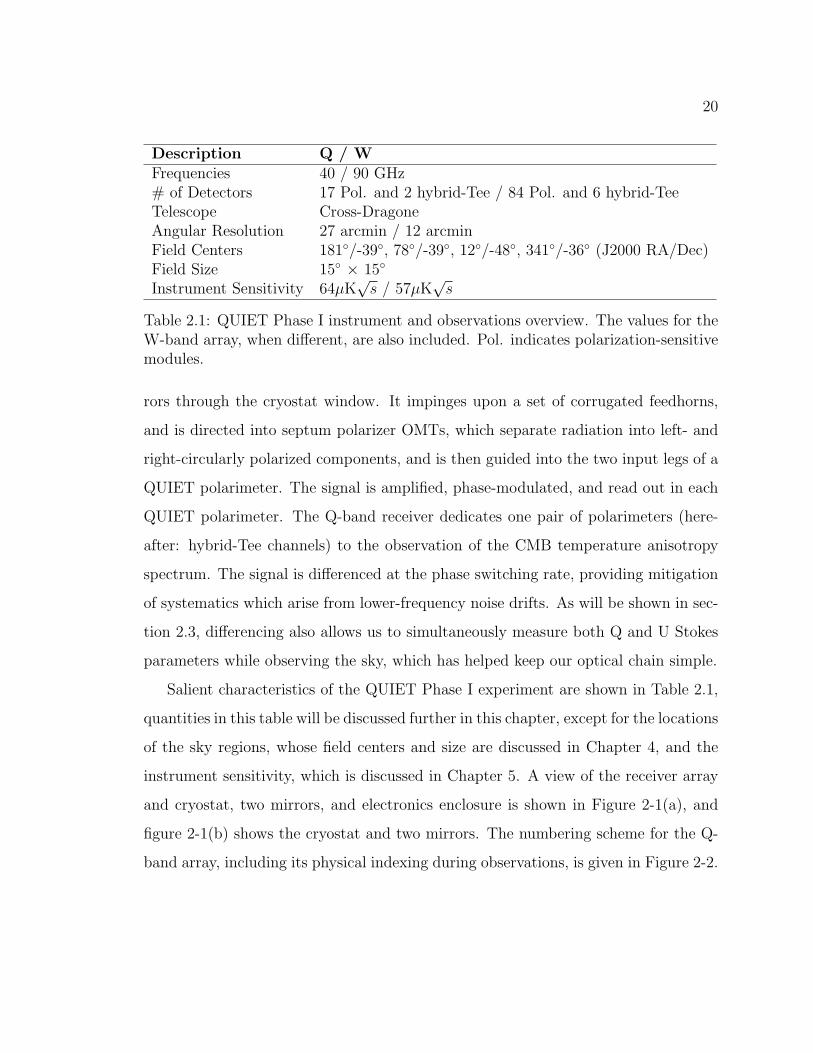
20
Description Q / WFrequencies 40 / 90 GHz# of Detectors 17 Pol. and 2 hybrid-Tee / 84 Pol. and 6 hybrid-TeeTelescope Cross-DragoneAngular Resolution 27 arcmin / 12 arcminField Centers 181/-39, 78/-39, 12/-48, 341/-36 (J2000 RA/Dec)Field Size 15 × 15
Instrument Sensitivity 64µK√
s / 57µK√
s
Table 2.1: QUIET Phase I instrument and observations overview. The values for theW-band array, when different, are also included. Pol. indicates polarization-sensitivemodules.
rors through the cryostat window. It impinges upon a set of corrugated feedhorns,
and is directed into septum polarizer OMTs, which separate radiation into left- and
right-circularly polarized components, and is then guided into the two input legs of a
QUIET polarimeter. The signal is amplified, phase-modulated, and read out in each
QUIET polarimeter. The Q-band receiver dedicates one pair of polarimeters (here-
after: hybrid-Tee channels) to the observation of the CMB temperature anisotropy
spectrum. The signal is differenced at the phase switching rate, providing mitigation
of systematics which arise from lower-frequency noise drifts. As will be shown in sec-
tion 2.3, differencing also allows us to simultaneously measure both Q and U Stokes
parameters while observing the sky, which has helped keep our optical chain simple.
Salient characteristics of the QUIET Phase I experiment are shown in Table 2.1,
quantities in this table will be discussed further in this chapter, except for the locations
of the sky regions, whose field centers and size are discussed in Chapter 4, and the
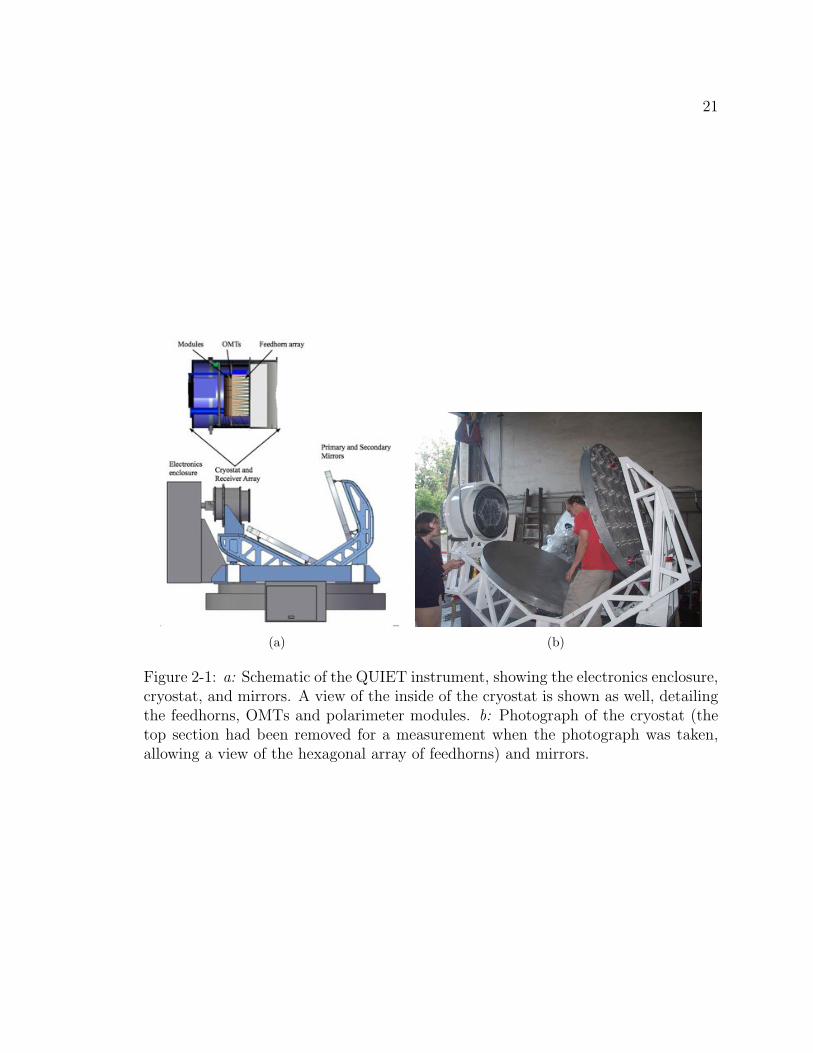
instrument sensitivity, which is discussed in Chapter 5. A view of the receiver array
and cryostat, two mirrors, and electronics enclosure is shown in Figure 2-1(a), and
figure 2-1(b) shows the cryostat and two mirrors. The numbering scheme for the Q-
band array, including its physical indexing during observations, is given in Figure 2-2.
21
(a) (b)
Figure 2-1: a: Schematic of the QUIET instrument, showing the electronics enclosure,cryostat, and mirrors. A view of the inside of the cryostat is shown as well, detailingthe feedhorns, OMTs and polarimeter modules. b: Photograph of the cryostat (thetop section had been removed for a measurement when the photograph was taken,allowing a view of the hexagonal array of feedhorns) and mirrors.
22
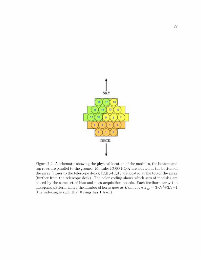
Figure 2-2: A schematic showing the physical location of the modules, the bottom andtop rows are parallel to the ground. Modules RQ00-RQ02 are located at the bottom ofthe array (closer to the telescope deck); RQ16-RQ18 are located at the top of the array(further from the telescope deck). The color coding shows which sets of modules arebiased by the same set of bias and data acquisition boards. Each feedhorn array is ahexagonal pattern, where the number of horns goes as Hfeeds with N rings = 3∗N2+3N+1(the indexing is such that 0 rings has 1 horn).
23
2.2 QUIET Optical Chain
2.2.1 Introduction
The QUIET optical chain consists of a Cross-Dragone side-fed dual-reflector system
coupled to an array of diffusion-bonded corrugated feeds. The feedhorns attach either
to a set of septum polarizer ortho-mode transducers (OMTs) or to hybrid-Tee assem-
blies. The output of those optical elements is directed into the QUIET polarimeters.
The measured performance of the system is found to be consistent with simulations
and all optical systematics are within the required specification to meet QUIET Phase
I science goals.
This section will address each of the components in the QUIET optical chain,
including design principles, expected performance, the design realization, and result-
ing sources of systematic error. Measurements presented in this section are based
on laboratory measurements; confirmation with astronomical calibrators during the
course of the observing season will be discussed in chapter 5.
2.2.2 Telescope Optics
Terminology
• Co-polarization: the fraction of linearly polarized light transmitted for a par-
ticular polarized state (Ex or Ey) given an input of the same state (Ex or Ey).
• Cross-polarization: the fraction of linearly polarized light transmitted for a
particular polarized state (Ex or Ey) given an input of the orthogonal state (Ey
or Ex). Typically this is used as a measurement of leakage from one polarization
state to the other. Cross-polarization leakage in an optical system is typically
quoted between linear polarization states Ex and Ey. For CMB polarization
systematics studies, we will also use the linear polarization Stokes Q and U
parameters to describe cross-polarization.

24
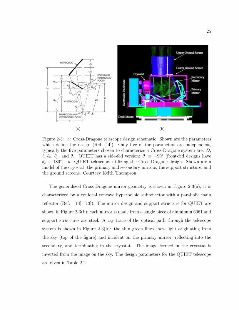
Parameter Description Value
D projected aperture of primary mirror 1.47 meS eccentricy of the (hyperbolic) secondary 2.244 distance between the two mirrors 1.27 mθ0 offset angle of the primary −53θe angle at which the feed sees the edges of the secondary 37θp angle between boresight of the feed and the axis of the secondary −90
Table 2.2: Parameters for the QUIET mirror design, see Ref. [42]. Positive (negative)angles are counterclockwise (clockwise) directions. These parameters are defined inthe Cross-Dragone design schematic in Figure 2-3(a).
• Spill-over: Any part of the beam which can ‘spill’ past an optical element,
illuminating regions other than the pointing of the main beam.
• Differential Ellipticity: the ellipticity of the beam for one linear polarization
state compared to the ellipticity of the beam for the orthogonal polarization
state.
Telescope Design Overview
The QUIET telescope design is a dual reflector Cross-Dragone system. The Cross-
Dragone design has numerous advantages for our polarization measurements (Ref. [14]):
• minimal spill-over past the mirrors
– limits pathways into the receiver from emission from scan synchronous
signals (e.g. the ground) and astronomical sources (e.g. the sun, moon).
• minimal cross-polarization characteristics
• uniform illumination across a large focal plane
– Optical distortions (such as astigmatism) can cause various forms of sys-
tematic errors, including increased cross-polarization. A flat beam charac-
terized by uniform mirror illumination will reduce these systematics.
25
(a) (b)
Figure 2-3: a: Cross-Dragone telescope design schematic. Shown are the parameterswhich define the design (Ref. [14]). Only five of the parameters are independent,typically the five parameters chosen to characterize a Cross-Dragone system are: D,, θ0, θp, and θe. QUIET has a side-fed version: θc ≡ −90 (front-fed designs haveθc ≡ 180). b: QUIET telescope, utilizing the Cross-Dragone design. Shown are amodel of the cryostat, the primary and secondary mirrors, the support structure, andthe ground screens. Courtesy Keith Thompson.
The generalized Cross-Dragone mirror geometry is shown in Figure 2-3(a); it is
characterized by a confocal concave hyperboloid subreflector with a parabolic main
reflector (Ref. [14], [13]). The mirror design and support structure for QUIET are
shown in Figure 2-3(b); each mirror is made from a single piece of aluminum 6061 and
support structures are steel. A ray trace of the optical path through the telescope
system is shown in Figure 2-3(b): the thin green lines show light originating from
the sky (top of the figure) and incident on the primary mirror, reflecting into the
secondary, and terminating in the cryostat. The image formed in the cryostat is
inverted from the image on the sky. The design parameters for the QUIET telescope
are given in Table 2.2.
26
Optical Design Goals and Systematics Limits
We determined a set of requirements for the optical design based on the science goals
for QUIET. These include:
• Beam Size: The diameter of each mirror was chosen such that QUIET would
be able to measure the first three peaks of the E-mode polarization spectrum
with the W-band receiver: with effective diameters of around 1.4m, the simu-
lated beamsize for the central horn at 42 GHz is 27.9 arcmin and 12.6 arcmin
at 90 GHz, corresponding to multipoles of up to 500, 900, respectively.
The beamwidth of the system has been measured with astronomical calibrators
during the observing season, those values will be discussed in chapter 5 and are
consistent with these design specifications.
• Differential ellipticity: Differential ellipticity will cause one polarization state
to be transmitted preferentially relative to the perpendicular polarization state,
systematically rotating the polarization direction of the incoming radiation.
Contributions from this instrumental polarization can be minimized by choosing
an observation strategy with multiple observing angles, as the polarization from
differential ellipticity will rotate with the telescope and so, unlike the sky signal,
will not remain constant in celestial coordinates. We require the differential
ellipticity to be < 10−3 (Ref. [22]).
• Cross-polarization leakage: this can contribute in much the same way as
differential ellipticity, the design requirement is that this systematic is < −40 dB
(0.01%) (Ref. [22]).
• Mirror Surface Quality: The surface of the mirrors was specified to have
distortions less than ±0.2mm and an RMS surface finish of 0.02mm-per-cm,
corresponding to λ37.5 and λ
375-per-cm (Q-band) and λ
17and λ
167-per-cm (W-
band).
27
2.2.3 Feedhorns and Interface Plate
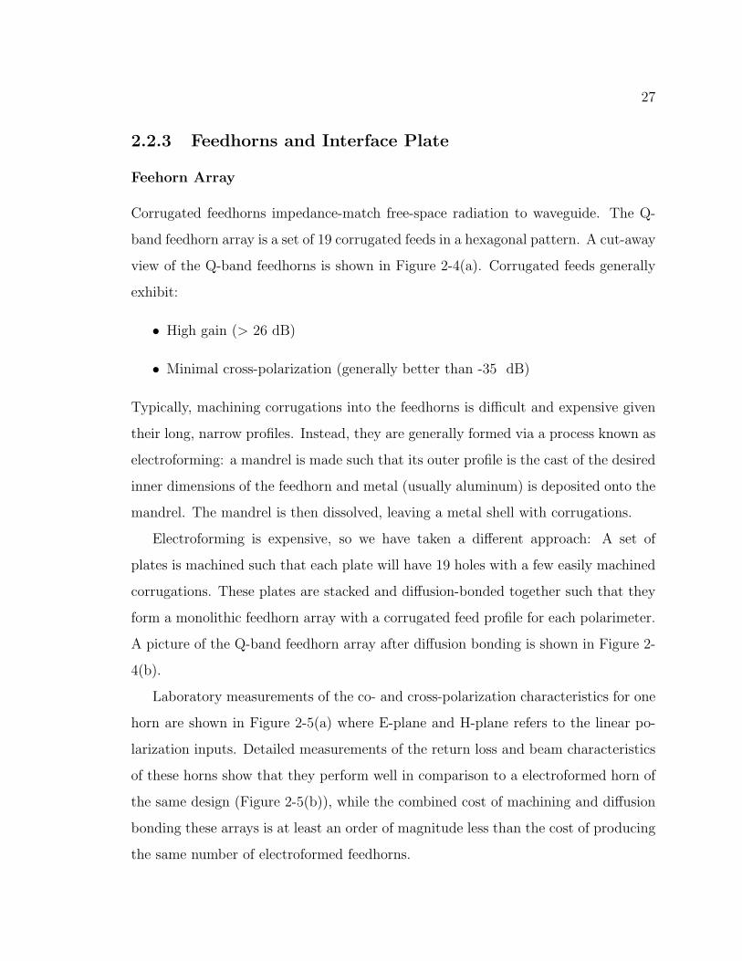
Feehorn Array
Corrugated feedhorns impedance-match free-space radiation to waveguide. The Q-
band feedhorn array is a set of 19 corrugated feeds in a hexagonal pattern. A cut-away
view of the Q-band feedhorns is shown in Figure 2-4(a). Corrugated feeds generally
exhibit:
• High gain (> 26 dB)
• Minimal cross-polarization (generally better than -35 dB)
Typically, machining corrugations into the feedhorns is difficult and expensive given
their long, narrow profiles. Instead, they are generally formed via a process known as
electroforming: a mandrel is made such that its outer profile is the cast of the desired
inner dimensions of the feedhorn and metal (usually aluminum) is deposited onto the
mandrel. The mandrel is then dissolved, leaving a metal shell with corrugations.
Electroforming is expensive, so we have taken a different approach: A set of
plates is machined such that each plate will have 19 holes with a few easily machined
corrugations. These plates are stacked and diffusion-bonded together such that they
form a monolithic feedhorn array with a corrugated feed profile for each polarimeter.
A picture of the Q-band feedhorn array after diffusion bonding is shown in Figure 2-
4(b).
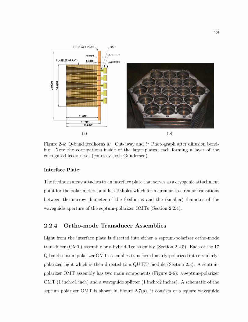
Laboratory measurements of the co- and cross-polarization characteristics for one
horn are shown in Figure 2-5(a) where E-plane and H-plane refers to the linear po-
larization inputs. Detailed measurements of the return loss and beam characteristics
of these horns show that they perform well in comparison to a electroformed horn of
the same design (Figure 2-5(b)), while the combined cost of machining and diffusion
bonding these arrays is at least an order of magnitude less than the cost of producing
the same number of electroformed feedhorns.
28
(a) (b)
Figure 2-4: Q-band feedhorns a: Cut-away and b: Photograph after diffusion bond-ing. Note the corrugations inside of the large plates, each forming a layer of thecorrugated feedorn set (courtesy Josh Gundersen).
Interface Plate
The feedhorn array attaches to an interface plate that serves as a cryogenic attachment
point for the polarimeters, and has 19 holes which form circular-to-circular transitions
between the narrow diameter of the feedhorns and the (smaller) diameter of the
waveguide aperture of the septum-polarizer OMTs (Section 2.2.4).
2.2.4 Ortho-mode Transducer Assemblies
Light from the interface plate is directed into either a septum-polarizer ortho-mode
transducer (OMT) assembly or a hybrid-Tee assembly (Section 2.2.5). Each of the 17
Q-band septum polarizer OMT assemblies transform linearly-polarized into circularly-
polarized light which is then directed to a QUIET module (Section 2.3). A septum-
polarizer OMT assembly has two main components (Figure 2-6): a septum-polarizer
OMT (1 inch×1 inch) and a waveguide splitter (1 inch×2 inches). A schematic of the
septum polarizer OMT is shown in Figure 2-7(a), it consists of a square waveguide
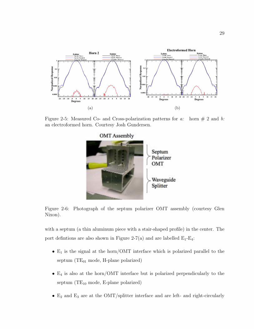
29
(a) (b)
Figure 2-5: Measured Co- and Cross-polarization patterns for a: horn # 2 and b:
an electroformed horn. Courtesy Josh Gundersen.
Figure 2-6: Photograph of the septum polarizer OMT assembly (courtesy GlenNixon).
with a septum (a thin aluminum piece with a stair-shaped profile) in the center. The
port defintions are also shown in Figure 2-7(a) and are labelled E1-E4:
• E1 is the signal at the horn/OMT interface which is polarized parallel to the
septum (TE01 mode, H-plane polarized)
• E4 is also at the horn/OMT interface but is polarized perpendicularly to the
septum (TE10 mode, E-plane polarized)
• E2 and E3 are at the OMT/splitter interface and are left- and right-circularly
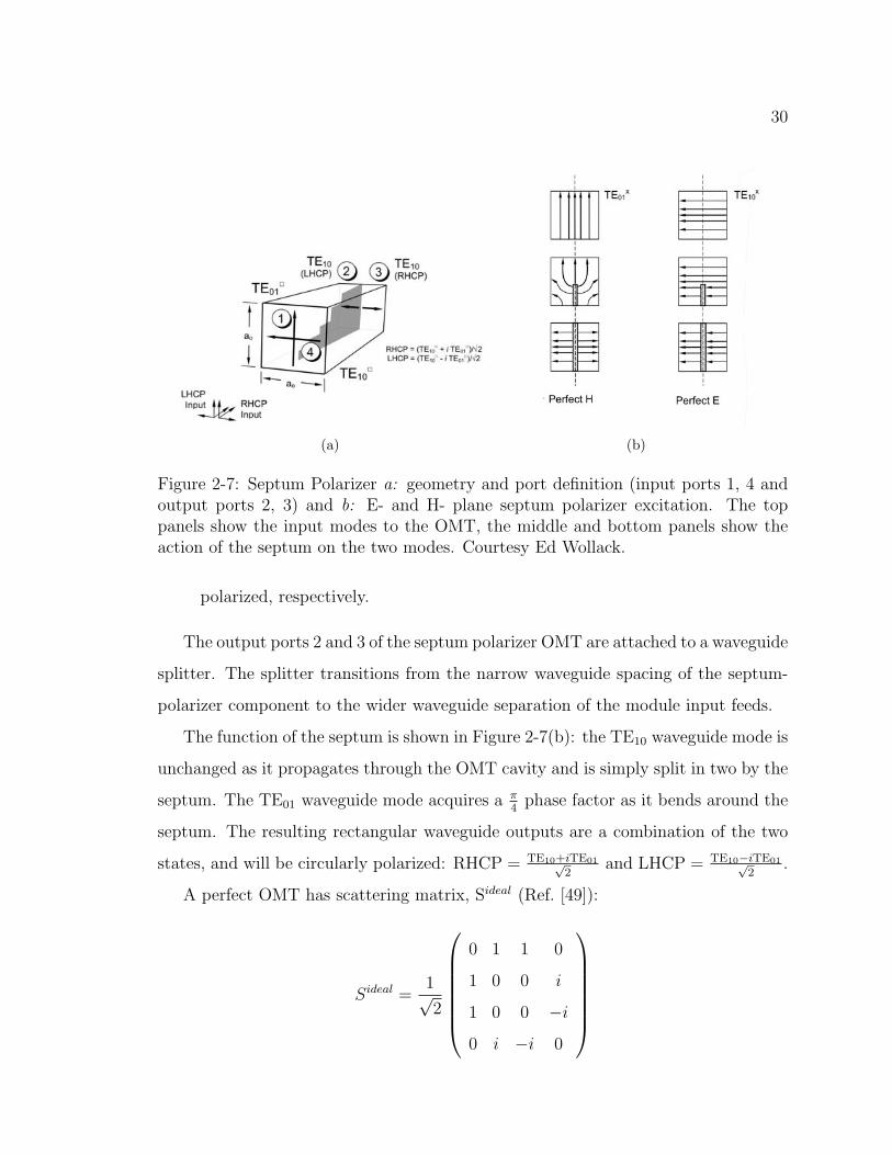
30
(a) (b)
Figure 2-7: Septum Polarizer a: geometry and port definition (input ports 1, 4 andoutput ports 2, 3) and b: E- and H- plane septum polarizer excitation. The toppanels show the input modes to the OMT, the middle and bottom panels show theaction of the septum on the two modes. Courtesy Ed Wollack.
polarized, respectively.
The output ports 2 and 3 of the septum polarizer OMT are attached to a waveguide
splitter. The splitter transitions from the narrow waveguide spacing of the septum-
polarizer component to the wider waveguide separation of the module input feeds.
The function of the septum is shown in Figure 2-7(b): the TE10 waveguide mode is
unchanged as it propagates through the OMT cavity and is simply split in two by the
septum. The TE01 waveguide mode acquires a π4
phase factor as it bends around the
septum. The resulting rectangular waveguide outputs are a combination of the two
states, and will be circularly polarized: RHCP = TE10+iTE01√2
and LHCP = TE10−iTE01√2
.
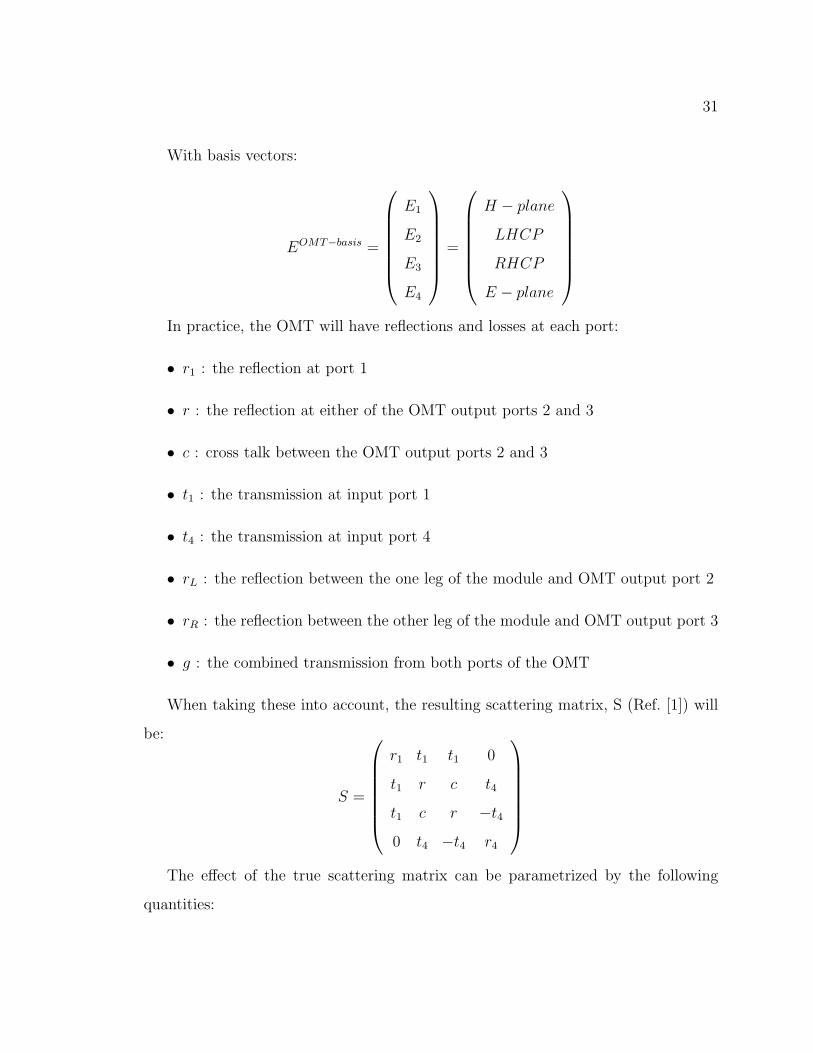
A perfect OMT has scattering matrix, Sideal (Ref. [49]):
Sideal =
1√
2
0 1 1 0
1 0 0 i
1 0 0 −i
0 i −i 0
31
With basis vectors:
EOMT−basis =
E1
E2
E3
E4
=
H − plane
LHCP
RHCP
E − plane
In practice, the OMT will have reflections and losses at each port:
• r1 : the reflection at port 1
• r : the reflection at either of the OMT output ports 2 and 3
• c : cross talk between the OMT output ports 2 and 3
• t1 : the transmission at input port 1
• t4 : the transmission at input port 4
• rL : the reflection between the one leg of the module and OMT output port 2
• rR : the reflection between the other leg of the module and OMT output port 3
• g : the combined transmission from both ports of the OMT
When taking these into account, the resulting scattering matrix, S (Ref. [1]) will
be:
S =
r1 t1 t1 0
t1 r c t4
t1 c r −t4
0 t4 −t4 r4
The effect of the true scattering matrix can be parametrized by the following
quantities:
32
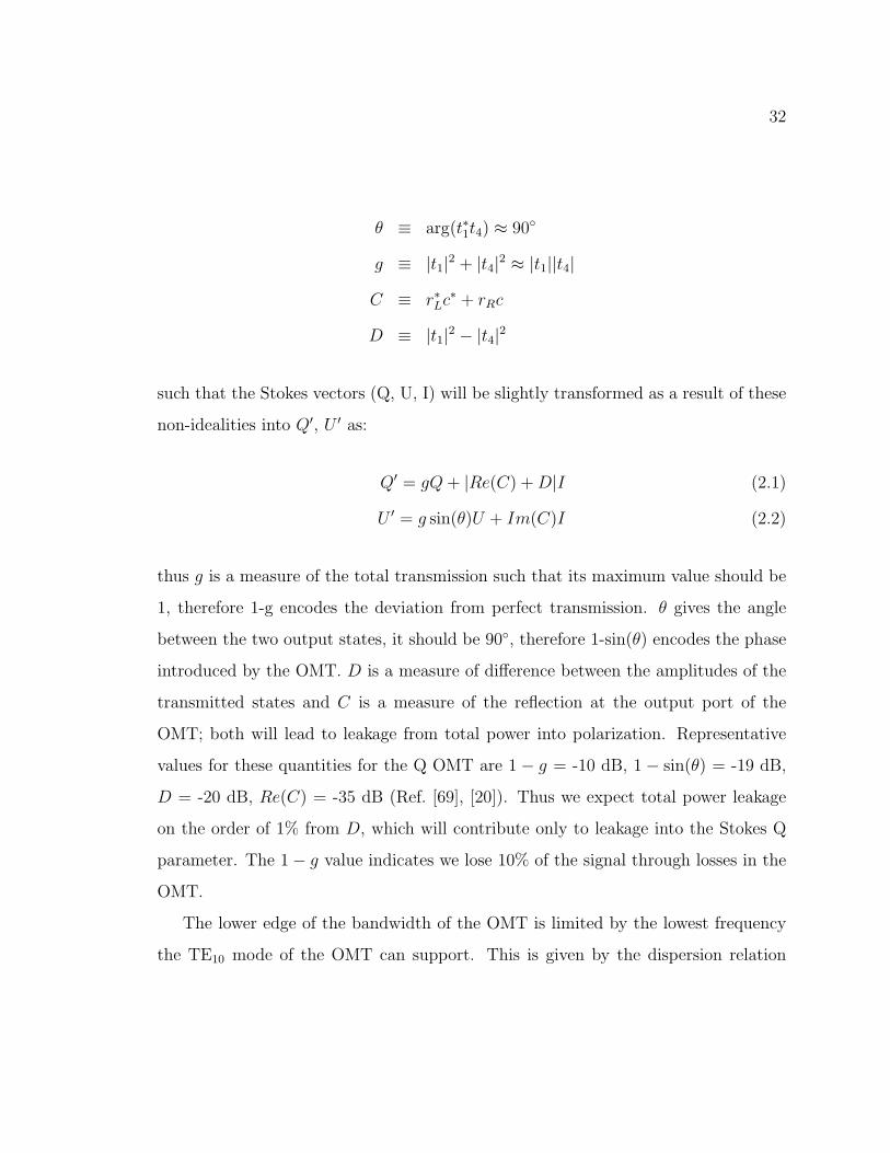
θ ≡ arg(t∗1t4) ≈ 90
g ≡ |t1|2 + |t4|
2≈ |t1||t4|
C ≡ r∗Lc∗ + rRc
D ≡ |t1|2− |t4|
2
such that the Stokes vectors (Q, U, I) will be slightly transformed as a result of these
non-idealities into Q, U
as:
Q = gQ + |Re(C) + D|I (2.1)
U = g sin(θ)U + Im(C)I (2.2)
thus g is a measure of the total transmission such that its maximum value should be
1, therefore 1-g encodes the deviation from perfect transmission. θ gives the angle
between the two output states, it should be 90, therefore 1-sin(θ) encodes the phase
introduced by the OMT. D is a measure of difference between the amplitudes of the
transmitted states and C is a measure of the reflection at the output port of the
OMT; both will lead to leakage from total power into polarization. Representative
values for these quantities for the Q OMT are 1− g = -10 dB, 1− sin(θ) = -19 dB,
D = -20 dB, Re(C) = -35 dB (Ref. [69], [20]). Thus we expect total power leakage
on the order of 1% from D, which will contribute only to leakage into the Stokes Q
parameter. The 1− g value indicates we lose 10% of the signal through losses in the
OMT.
The lower edge of the bandwidth of the OMT is limited by the lowest frequency
the TE10 mode of the OMT can support. This is given by the dispersion relation
33
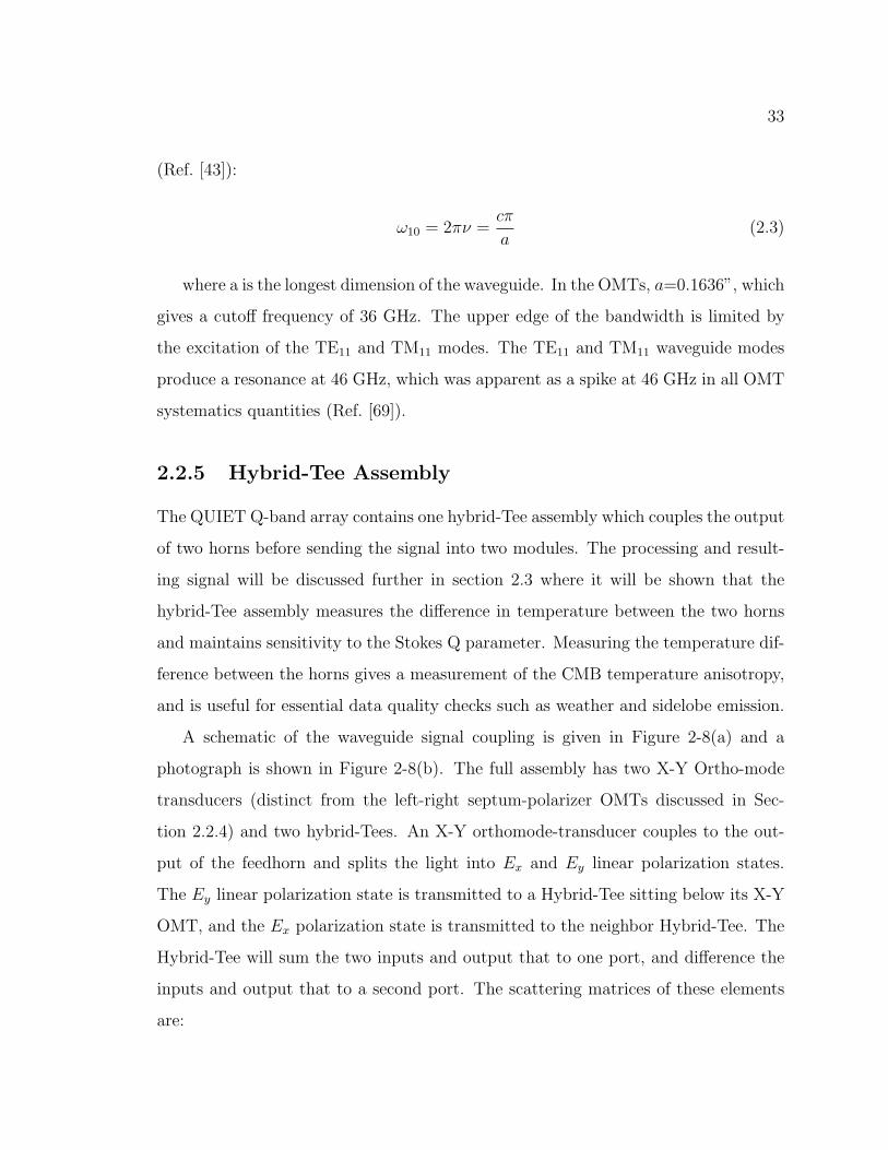
(Ref. [43]):
ω10 = 2πν =cπ
a(2.3)
where a is the longest dimension of the waveguide. In the OMTs, a=0.1636”, which
gives a cutoff frequency of 36 GHz. The upper edge of the bandwidth is limited by
the excitation of the TE11 and TM11 modes. The TE11 and TM11 waveguide modes
produce a resonance at 46 GHz, which was apparent as a spike at 46 GHz in all OMT
systematics quantities (Ref. [69]).
2.2.5 Hybrid-Tee Assembly
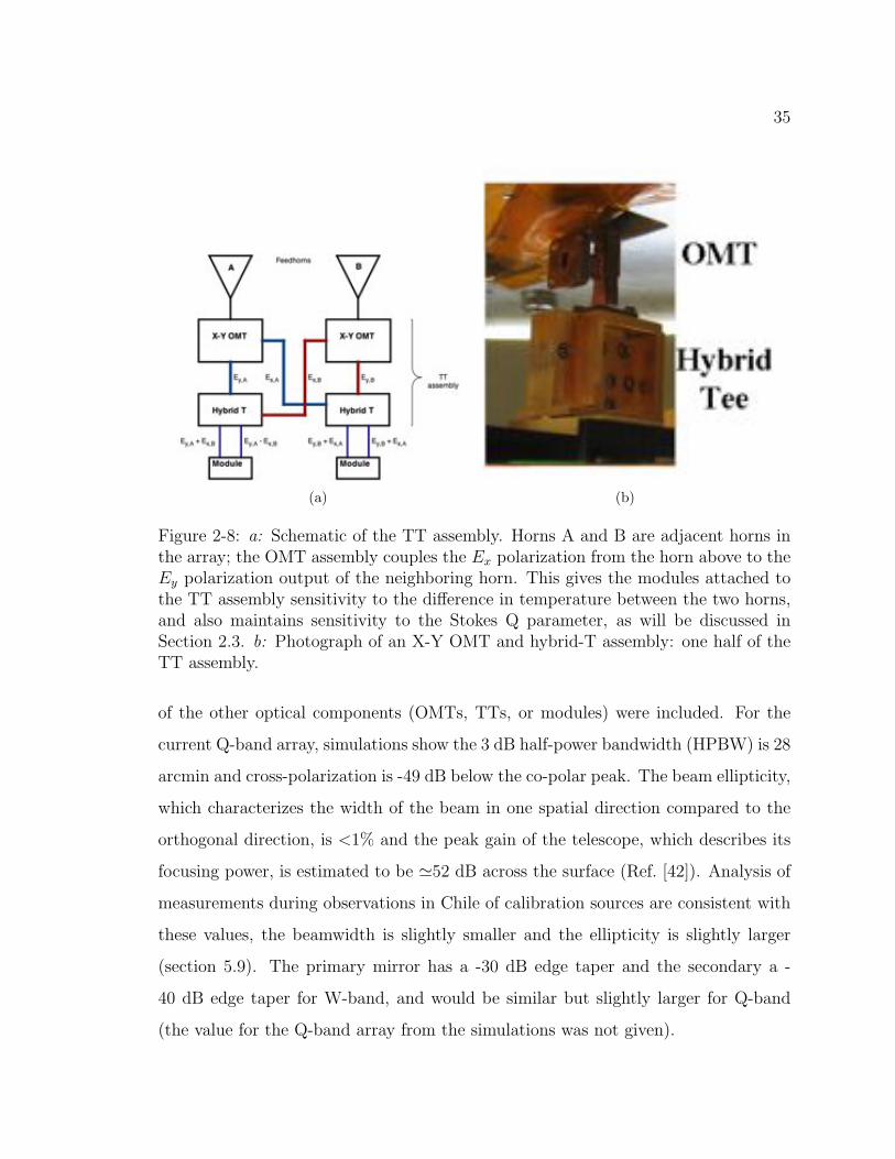
The QUIET Q-band array contains one hybrid-Tee assembly which couples the output
of two horns before sending the signal into two modules. The processing and result-
ing signal will be discussed further in section 2.3 where it will be shown that the
hybrid-Tee assembly measures the difference in temperature between the two horns
and maintains sensitivity to the Stokes Q parameter. Measuring the temperature dif-
ference between the horns gives a measurement of the CMB temperature anisotropy,
and is useful for essential data quality checks such as weather and sidelobe emission.
A schematic of the waveguide signal coupling is given in Figure 2-8(a) and a
photograph is shown in Figure 2-8(b). The full assembly has two X-Y Ortho-mode
transducers (distinct from the left-right septum-polarizer OMTs discussed in Sec-
tion 2.2.4) and two hybrid-Tees. An X-Y orthomode-transducer couples to the out-
put of the feedhorn and splits the light into Ex and Ey linear polarization states.
The Ey linear polarization state is transmitted to a Hybrid-Tee sitting below its X-Y
OMT, and the Ex polarization state is transmitted to the neighbor Hybrid-Tee. The
Hybrid-Tee will sum the two inputs and output that to one port, and difference the
inputs and output that to a second port. The scattering matrices of these elements
are:
34
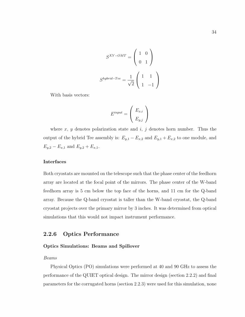
SXY−OMT =
1 0
0 1
Shybrid−Tee =
1√
2
1 1
1 −1
With basis vectors:
Einput =
Ex,i
Ey,j
where x, y denotes polarization state and i, j denotes horn number. Thus the
output of the hybrid Tee assembly is: Ey,1−Ex,2 and Ey,1 + Ex,2 to one module, and
Ey,2 − Ex,1 and Ey,2 + Ex,1.
Interfaces
Both cryostats are mounted on the telescope such that the phase center of the feedhorn
array are located at the focal point of the mirrors. The phase center of the W-band
feedhorn array is 5 cm below the top face of the horns, and 11 cm for the Q-band
array. Because the Q-band cryostat is taller than the W-band cryostat, the Q-band
cryostat projects over the primary mirror by 3 inches. It was determined from optical
simulations that this would not impact instrument performance.
2.2.6 Optics Performance
Optics Simulations: Beams and Spillover
Beams
Physical Optics (PO) simulations were performed at 40 and 90 GHz to assess the
performance of the QUIET optical design. The mirror design (section 2.2.2) and final
parameters for the corrugated horns (section 2.2.3) were used for this simulation, none
35
(a) (b)
Figure 2-8: a: Schematic of the TT assembly. Horns A and B are adjacent horns inthe array; the OMT assembly couples the Ex polarization from the horn above to theEy polarization output of the neighboring horn. This gives the modules attached tothe TT assembly sensitivity to the difference in temperature between the two horns,and also maintains sensitivity to the Stokes Q parameter, as will be discussed inSection 2.3. b: Photograph of an X-Y OMT and hybrid-T assembly: one half of theTT assembly.
of the other optical components (OMTs, TTs, or modules) were included. For the
current Q-band array, simulations show the 3 dB half-power bandwidth (HPBW) is 28
arcmin and cross-polarization is -49 dB below the co-polar peak. The beam ellipticity,
which characterizes the width of the beam in one spatial direction compared to the
orthogonal direction, is <1% and the peak gain of the telescope, which describes its
focusing power, is estimated to be 52 dB across the surface (Ref. [42]). Analysis of
measurements during observations in Chile of calibration sources are consistent with
these values, the beamwidth is slightly smaller and the ellipticity is slightly larger
(section 5.9). The primary mirror has a -30 dB edge taper and the secondary a -
40 dB edge taper for W-band, and would be similar but slightly larger for Q-band
(the value for the Q-band array from the simulations was not given).
36
Beam performance will change with location in the focal plane. To evaluate the
effects of cross-polarization leakage on the edge horns, two simulations with orthogo-
nal polarization states were performed: they are denoted as ‘Ex’ and ‘Ey’ (as the horn
looks at the secondary, ‘Ex’ is in the horizontal direction and ‘Ey’ is in the vertical
direction). With an input state of ‘Ex’, the simulated response can be measured in
the parallel polarization state, yielding a measurement of co-polar beam throughput
and ellipticity for one polarization input state. A simulation with an input state of
‘Ex’ and a measured response in the orthogonal state yields a measurement of the
cross-polarization characteristics of the system. This can be repeated with an input
of ‘Ey’ and measurements in ‘Ey’ and ‘Ex’. The differences in beam ellipticities be-
tween the two co-polar measurements is the differential ellipticity. The results of the
simulation are summarized in Table 2.3 and the beam shapes for the central horn and
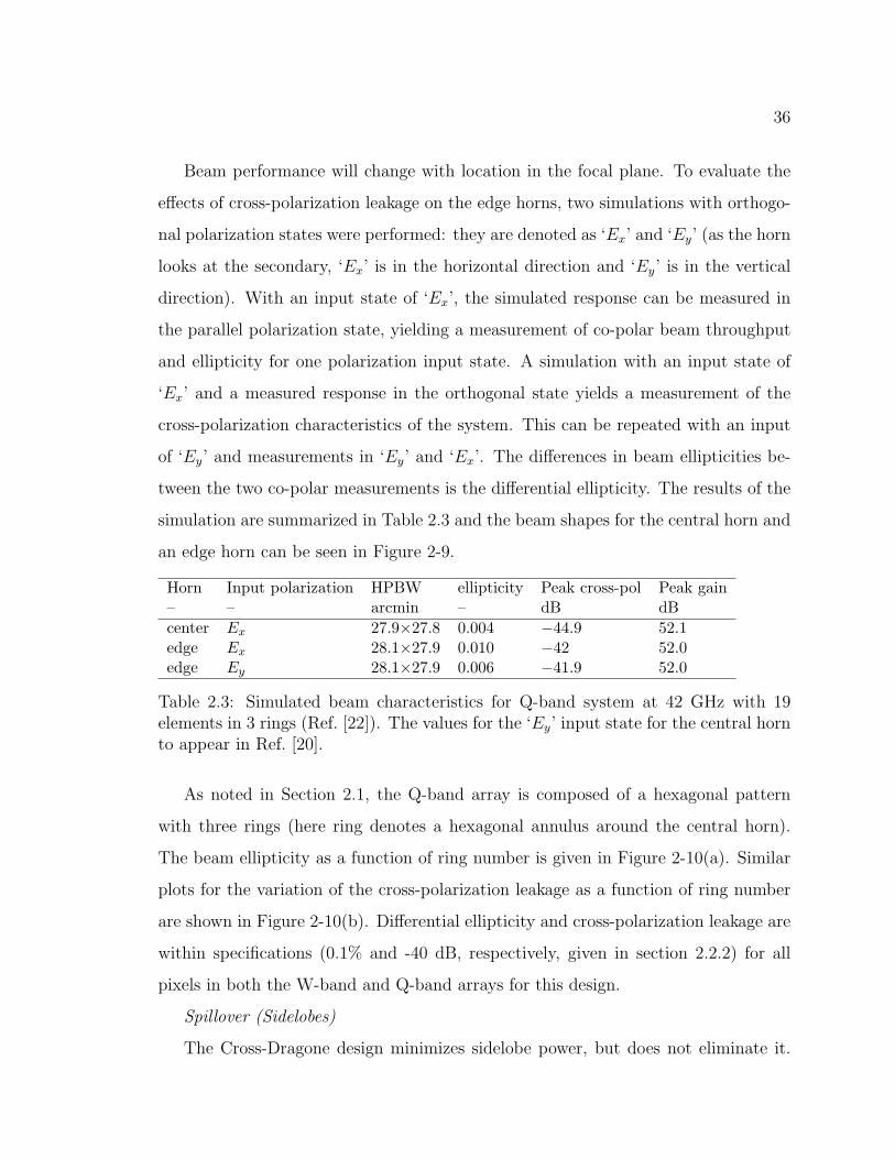
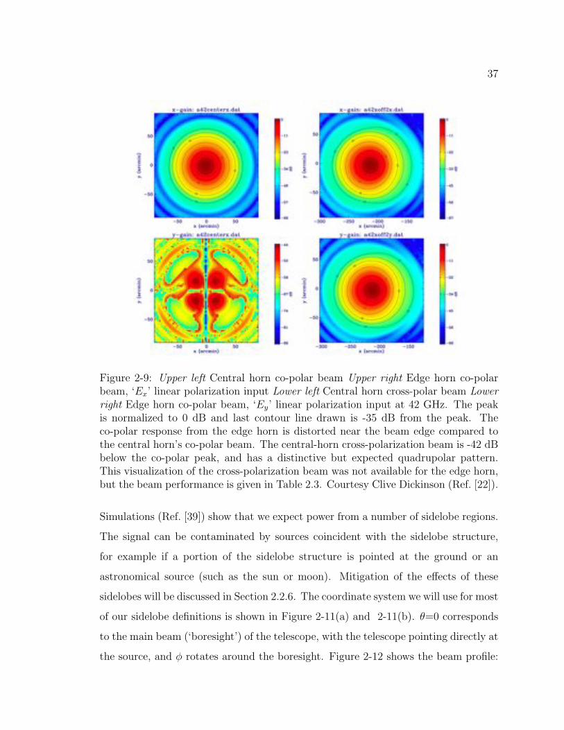
an edge horn can be seen in Figure 2-9.
Horn Input polarization HPBW ellipticity Peak cross-pol Peak gain– – arcmin – dB dBcenter Ex 27.9×27.8 0.004 −44.9 52.1edge Ex 28.1×27.9 0.010 −42 52.0edge Ey 28.1×27.9 0.006 −41.9 52.0
Table 2.3: Simulated beam characteristics for Q-band system at 42 GHz with 19elements in 3 rings (Ref. [22]). The values for the ‘Ey’ input state for the central hornto appear in Ref. [20].
As noted in Section 2.1, the Q-band array is composed of a hexagonal pattern
with three rings (here ring denotes a hexagonal annulus around the central horn).
The beam ellipticity as a function of ring number is given in Figure 2-10(a). Similar
plots for the variation of the cross-polarization leakage as a function of ring number
are shown in Figure 2-10(b). Differential ellipticity and cross-polarization leakage are
within specifications (0.1% and -40 dB, respectively, given in section 2.2.2) for all
pixels in both the W-band and Q-band arrays for this design.
Spillover (Sidelobes)
The Cross-Dragone design minimizes sidelobe power, but does not eliminate it.
37
Figure 2-9: Upper left Central horn co-polar beam Upper right Edge horn co-polarbeam, ‘Ex’ linear polarization input Lower left Central horn cross-polar beam Lower
right Edge horn co-polar beam, ‘Ey’ linear polarization input at 42 GHz. The peakis normalized to 0 dB and last contour line drawn is -35 dB from the peak. Theco-polar response from the edge horn is distorted near the beam edge compared tothe central horn’s co-polar beam. The central-horn cross-polarization beam is -42 dBbelow the co-polar peak, and has a distinctive but expected quadrupolar pattern.This visualization of the cross-polarization beam was not available for the edge horn,but the beam performance is given in Table 2.3. Courtesy Clive Dickinson (Ref. [22]).
Simulations (Ref. [39]) show that we expect power from a number of sidelobe regions.
The signal can be contaminated by sources coincident with the sidelobe structure,
for example if a portion of the sidelobe structure is pointed at the ground or an
astronomical source (such as the sun or moon). Mitigation of the effects of these
sidelobes will be discussed in Section 2.2.6. The coordinate system we will use for most
of our sidelobe definitions is shown in Figure 2-11(a) and 2-11(b). θ=0 corresponds
to the main beam (‘boresight’) of the telescope, with the telescope pointing directly at
the source, and φ rotates around the boresight. Figure 2-12 shows the beam profile:
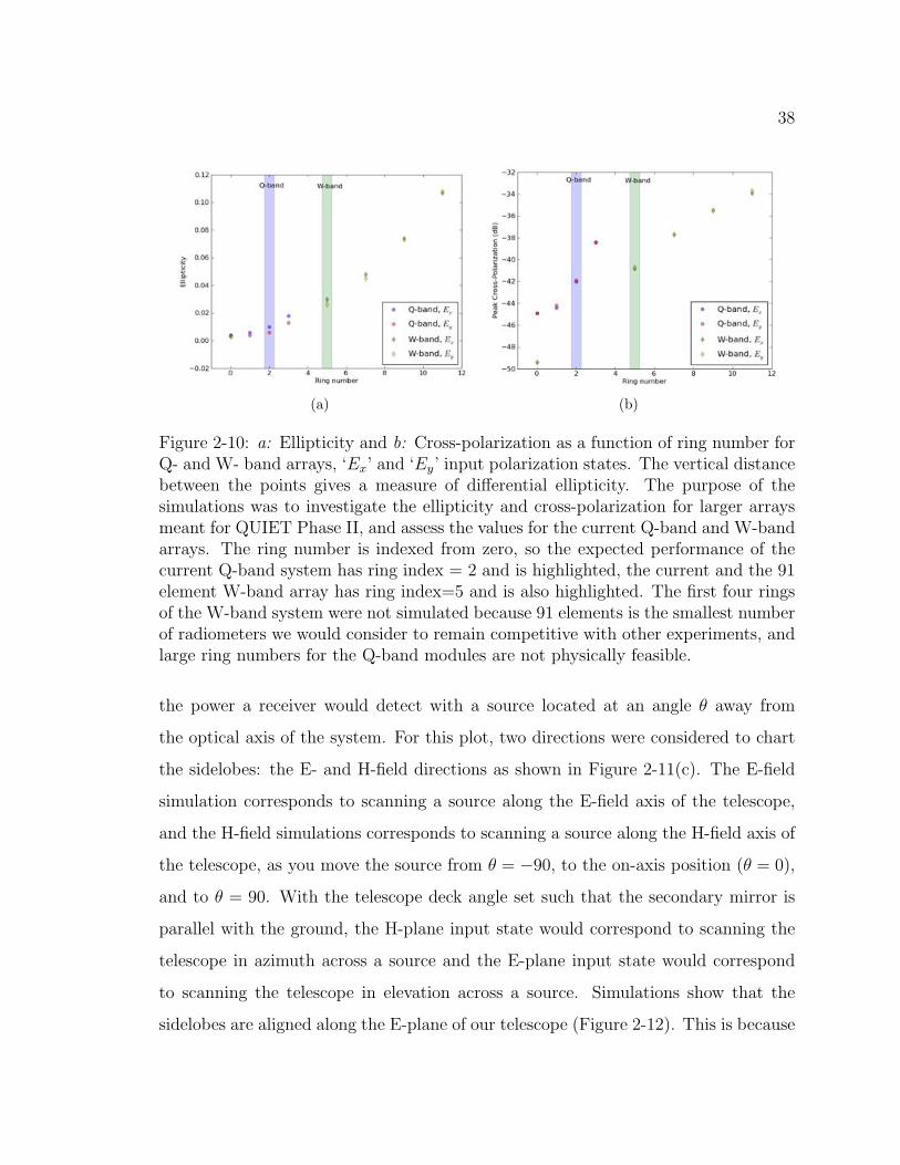
38
(a) (b)
Figure 2-10: a: Ellipticity and b: Cross-polarization as a function of ring number forQ- and W- band arrays, ‘Ex’ and ‘Ey’ input polarization states. The vertical distancebetween the points gives a measure of differential ellipticity. The purpose of thesimulations was to investigate the ellipticity and cross-polarization for larger arraysmeant for QUIET Phase II, and assess the values for the current Q-band and W-bandarrays. The ring number is indexed from zero, so the expected performance of thecurrent Q-band system has ring index = 2 and is highlighted, the current and the 91element W-band array has ring index=5 and is also highlighted. The first four ringsof the W-band system were not simulated because 91 elements is the smallest numberof radiometers we would consider to remain competitive with other experiments, andlarge ring numbers for the Q-band modules are not physically feasible.
the power a receiver would detect with a source located at an angle θ away from
the optical axis of the system. For this plot, two directions were considered to chart
the sidelobes: the E- and H-field directions as shown in Figure 2-11(c). The E-field
simulation corresponds to scanning a source along the E-field axis of the telescope,
and the H-field simulations corresponds to scanning a source along the H-field axis of
the telescope, as you move the source from θ = −90, to the on-axis position (θ = 0),
and to θ = 90. With the telescope deck angle set such that the secondary mirror is
parallel with the ground, the H-plane input state would correspond to scanning the
telescope in azimuth across a source and the E-plane input state would correspond
to scanning the telescope in elevation across a source. Simulations show that the
sidelobes are aligned along the E-plane of our telescope (Figure 2-12). This is because
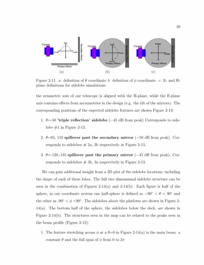
39
(a) (b) (c)
Figure 2-11: a: definition of θ coordinate b: definition of φ coordinate. c: E- and H-plane definitions for sidelobe simulations.
the symmetric axis of our telescope is aligned with the H-plane, while the E-plane
axis contains effects from asymmetries in the design (e.g. the tilt of the mirrors). The
corresponding positions of the expected sidelobe features are shown Figure 2-13:
1. θ=-50 ’triple reflection’ sidelobe (−45 dB from peak) Corresponds to side-
lobe #1 in Figure 2-13.
2. θ=65, 110 spillover past the secondary mirror (−50 dB from peak). Cor-
responds to sidelobes # 2a, 2b respectively in Figure 2-13.
3. θ=-120,-135 spillover past the primary mirror (−45 dB from peak). Cor-
responds to sidelobes # 3b, 3a respectively in Figure 2-13.
We can gain additional insight from a 2D plot of the sidelobe locations, including
the shape of each of these lobes. The full two dimensional sidelobe structure can be
seen in the combination of Figures 2-14(a) and 2-14(b). Each figure is half of the
sphere, in our coordinate system one half-sphere is defined as −90 < θ < 90 and
the other as -90 < φ <90. The sidelobes above the platform are shown in Figure 2-
14(a). The bottom half of the sphere, the sidelobes below the deck, are shown in
Figure 2-14(b). The structures seen in the map can be related to the peaks seen in
the beam profile (Figure 2-12):
1. The feature stretching across φ at a θ=0 in Figure 2-14(a) is the main beam: a
constant θ and the full span of φ from 0 to 2π
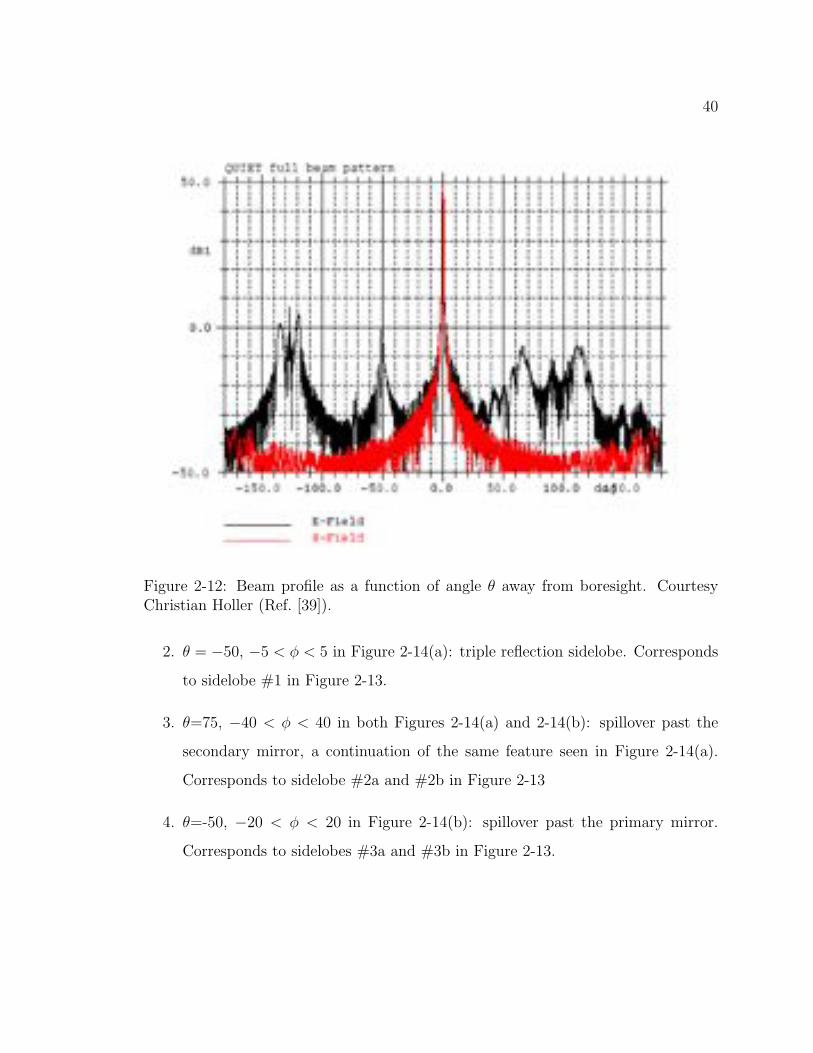
40
Figure 2-12: Beam profile as a function of angle θ away from boresight. CourtesyChristian Holler (Ref. [39]).
2. θ = −50, −5 < φ < 5 in Figure 2-14(a): triple reflection sidelobe. Corresponds
to sidelobe #1 in Figure 2-13.
3. θ=75, −40 < φ < 40 in both Figures 2-14(a) and 2-14(b): spillover past the
secondary mirror, a continuation of the same feature seen in Figure 2-14(a).
Corresponds to sidelobe #2a and #2b in Figure 2-13
4. θ=-50, −20 < φ < 20 in Figure 2-14(b): spillover past the primary mirror.
Corresponds to sidelobes #3a and #3b in Figure 2-13.
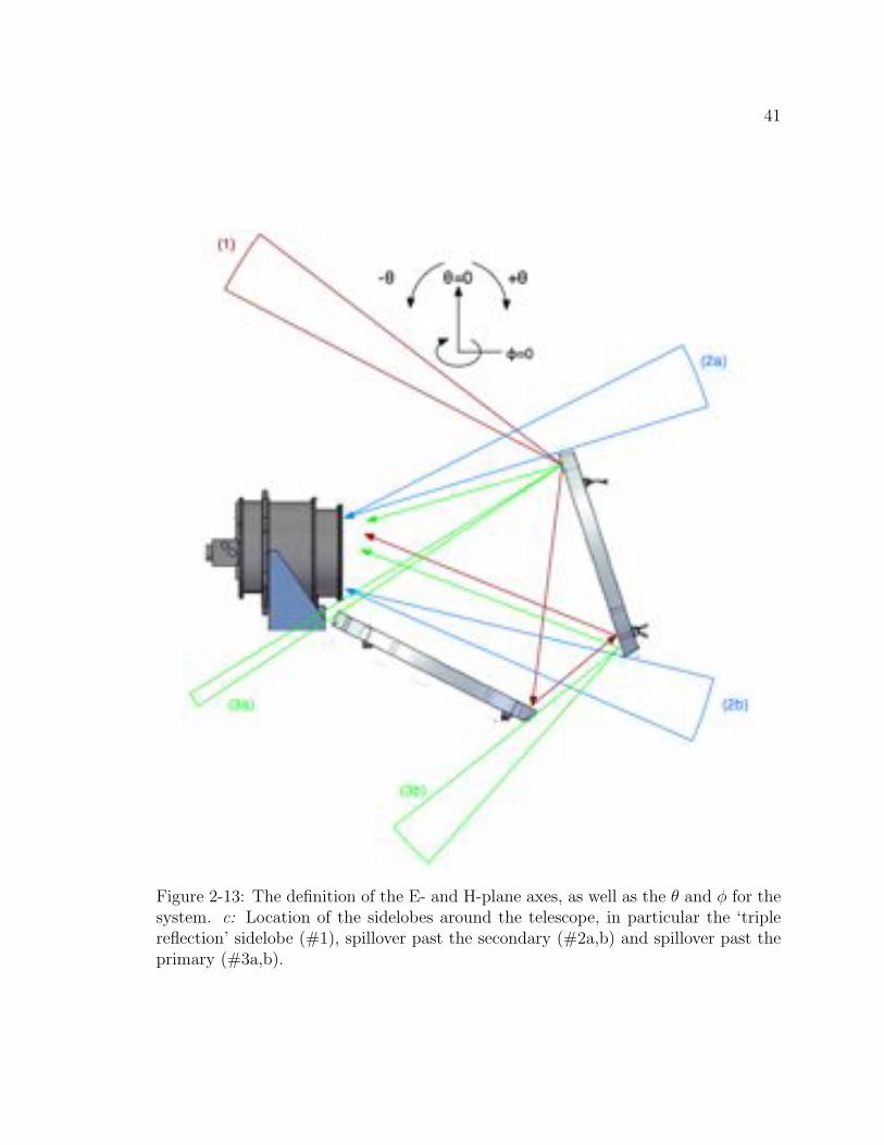
41
Figure 2-13: The definition of the E- and H-plane axes, as well as the θ and φ for thesystem. c: Location of the sidelobes around the telescope, in particular the ‘triplereflection’ sidelobe (#1), spillover past the secondary (#2a,b) and spillover past theprimary (#3a,b).
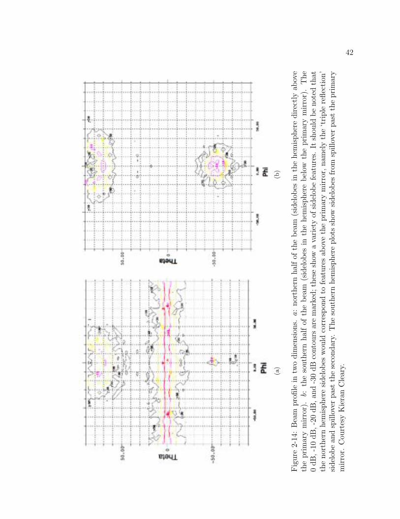
42
(a)
(b)
Fig
ure
2-14
:B
eam
pro
file
intw
odim
ensi
ons.
a:
nor
ther
nhal
fof
the
bea
m(s
idel
obes
inth
ehem
ispher
edir
ectl
yab
ove
the
pri
mar
ym
irro
r).
b:
the
south
ern
hal
fof
the
bea
m(s
idel
obes
inth
ehem
ispher
ebel
owth
epri
mar
ym
irro
r).
The
0dB
,-1
0dB
,-2
0dB
,an
d-3
0dB
cont
ours
are
mar
ked;th
ese
show
ava
riet
yof
sidel
obe
feat
ure
s.It
shou
ldbe
not
edth
atth
enor
ther
nhem
ispher
esi
del
obes
wou
ldco
rres
pon
dto
feat
ure
sab
ove
the
prim
ary
mir
ror,
nam
ely
the
‘tri
ple
reflec
tion
’si
del
obe
and
spillo
ver
pas
tth
ese
condar
y.T
he
south
ern
hem
ispher
eplo
tssh
owsi
del
obes
from
spillo
ver
pas
tth
epri
mar
ym
irro
r.C
ourt
esy
Kie
ran
Cle
ary.
43
The sidelobe structures in the two dimensional plot are symmetric around θ, in
the sense that for a particular φ point, the structure at +θ is the mirror image of
that at −θ. This confirms that the symmetric axis of the telescope runs along the
primary mirror (perpendicular to a vector drawn between the secondary mirror and
the cryostat).
Design Tolerances
We considered a variety of effects to understand and characterize our optical design
tolerances. These include the position of the feedhorns with respect to the focus of
the mirrors, the effects of thermal contraction and expansion on the positions of the
mirrors while observing in the field, and the surface finish of the mirrors.
The QUIET optical system is ‘slow’; the rays coming from the secondary mirror
and converging into the cryostat do not converge at a particularly acute angle, and
so the tolerance for the location of the feedhorns with respect to the focus of the
telescope is generous. Shifts of the feedhorns within the mirror system of ±1 cm will
still yield beam cross-polarization and ellipticity values within specifications. This
slow convergence minimizes the impact of thermal contraction and expansion on the
system as well, which can cause shifts of up to 4mm1.
Alignment was performed in Chile, the mirrors were aligned to within 400µm of
the true 3D mirror model, this is within the specifications developed from optical sim-
ulations. In addition, the Q-band cryostat hangs over the primary mirror by 3 inches;
it was determined that this did not compromise instrument performance because the
telescope edge taper is -30 dB, enough that there is insignificant contribution to the
beam from this region of the mirrors.
Light incident on the mirror will bounce off of any surface irregularities, decreasing
instrument sensitivity and increasing power in the beam sidelobes. The scattering
1The length of the support structure between the two mirrors is around 1.4 m, with typicaltemperature variation of 40F and a coefficient of thermal expansion for steel of 7 ×10⁻⁶ inches/inchF (http:www.matweb.com) gives an expansion value of 4mm.
44
amplitude and angular dependence is a function of the size of the irregularities relative
to the observing wavelength. This effect was quantified by Ruze (Ref. [76]). After
machining, both the primary and secondary mirror surfaces were measured. These
measurements were used to simulate the main beam and sidelobe structure for the 90
GHz beam, shown in Figure 2-15. Generally surface irregularities will scatter power
from the main beam into the sidelobes, this is not apparent from Figure 2-15 because
the peak of both the measurements and simulations were normalized to one.
Scattering scales with frequency, such that the surface irregularities will impact
the sidelobe structure of the Q-band array to a smaller degree; this is apparent in
comparisons between beam gain from the simulations (52.1 dB gain, section 2.2.6
Table 2.3) and from measurements with calibration sources (52.4 dB gain, section 5.9).
Ground-Screen
To minimize contamination from the ground and astronomical sources entering the
data stream via sidelobe spillover, we designed an absorbing ground-screen to shield
the mirrors from the ground and so allow the sidelobes to terminate on a constant
temperature source. The ground-screen structure, shown in Figure 2-3(b), consists of
two parts: an aluminum box (‘Ground Screen’), which encloses both mirrors and the
front half of the cryostat, and a cylindrical tube that attaches to the ground screen
directly above the primary mirror (‘Upper Ground Screen’). The external surface
of the ground-screen was coated in white paint to minimize radiative loading and
reduce diurnal temperature variations. The interior of the ground-screen was coated
with a broad-band absorber (Emerson Cumming HR-10) which absorbs radiation and
re-emitts it at a constant temperature, allowing the ground-screen to function as an
approximately constant black-body source in both Q- and W- band frequencies. The
absorptive ground-screen shields the instrument from ground pick-up and provide a
stable, unpolarized emission source, which does not vary during a telescope scan (as
the ground or an astronomical source would). The absorber was coated with sheets
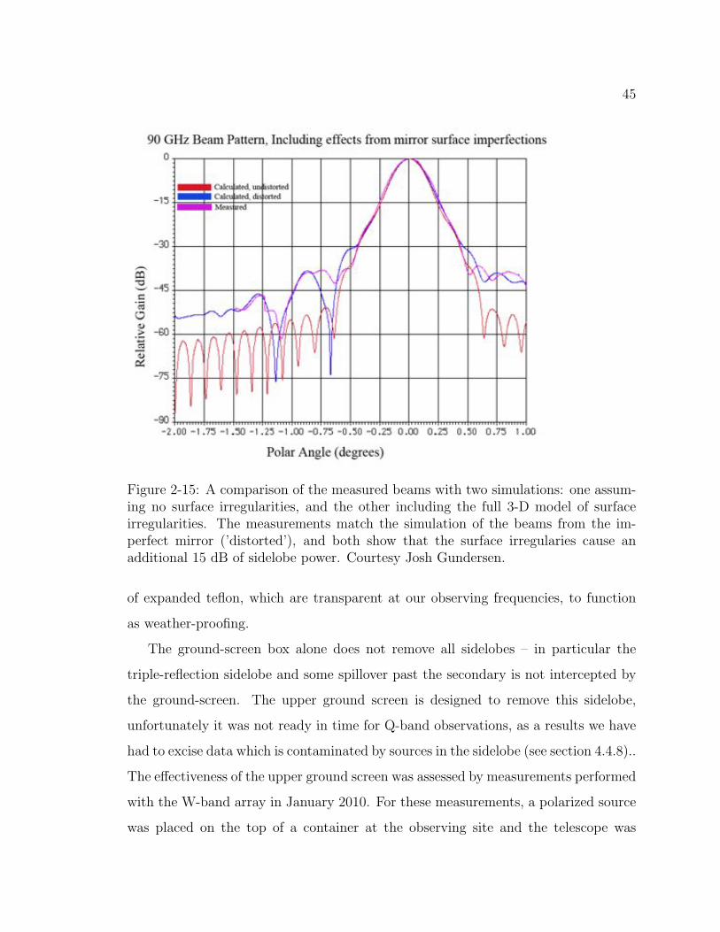
45
Figure 2-15: A comparison of the measured beams with two simulations: one assum-ing no surface irregularities, and the other including the full 3-D model of surfaceirregularities. The measurements match the simulation of the beams from the im-perfect mirror (’distorted’), and both show that the surface irregularies cause anadditional 15 dB of sidelobe power. Courtesy Josh Gundersen.
of expanded teflon, which are transparent at our observing frequencies, to function
as weather-proofing.
The ground-screen box alone does not remove all sidelobes – in particular the
triple-reflection sidelobe and some spillover past the secondary is not intercepted by
the ground-screen. The upper ground screen is designed to remove this sidelobe,
unfortunately it was not ready in time for Q-band observations, as a results we have
had to excise data which is contaminated by sources in the sidelobe (see section 4.4.8)..
The effectiveness of the upper ground screen was assessed by measurements performed
with the W-band array in January 2010. For these measurements, a polarized source
was placed on the top of a container at the observing site and the telescope was
46
scanned over its entire azimuth and elevation range (−180 to 200 azimuth, 43 to
75 elevation) at four different deck angles (0, 90, −90, −180). When the telescope
scans a region where the source has a path into the receiver through a sidelobe,
the radiometers detect a higher signal than background noise. We performed the
measurements without the upper ground screen section and then repeated them with
this upper section included. As seen in Figures 2-16(a), 2-16(b), the main sidelobe
feature at the bottom of the map, which in this case corresponds to spillover past
the secondary, was removed. Additional sidelobe flares were discovered which were
caused by holes in the floor of the ground screen. A third measurement was taken
after placing absorber over these holes (Figure 2-16(c)).
The ground screen is designed to shield the optics from ground emission. Be-
cause it is an absorbing groundscreen, changes in the ground screen temperatures
will change the emission temperature and could potentially be detected by the po-
larimeters through sidelobe pickup. To monitor the temperature of the ground screen,
we placed 26 temperature sensors on various external surfaces of the ground screen,
mirrors, and cryostat (shown in Figures 2-17(a) and 2-17(b)).
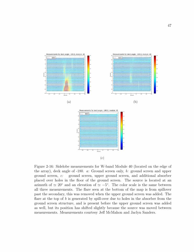
47
(a) (b)
(c)
Figure 2-16: Sidelobe measurements for W-band Module 40 (located on the edge ofthe array), deck angle of -180. a: Ground screen only, b: ground screen and upperground screen, c: ground screen, upper ground screen, and additional absorberplaced over holes in the floor of the ground screen. The source is located at anazimuth of 20 and an elevation of −5. The color scale is the same betweenall three measurements. The flare seen at the bottom of the map is from spilloverpast the secondary, this was removed when the upper ground screen was added. Theflare at the top of b is generated by spill-over due to holes in the absorber from theground screen structure, and is present before the upper ground screen was addedas well, but its position has shifted slightly because the source was moved betweenmeasurements. Measurements courtesy Jeff McMahon and Jaclyn Sanders.
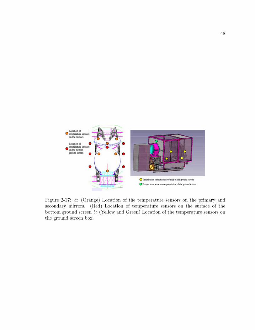
48
Figure 2-17: a: (Orange) Location of the temperature sensors on the primary andsecondary mirrors. (Red) Location of temperature sensors on the surface of thebottom ground screen b: (Yellow and Green) Location of the temperature sensors onthe ground screen box.
49
2.3 Polarimeter Modules
2.3.1 Introduction
Each QUIET module is a polarimeter employing High-electron-mobility transistor
(HEMT) technology for amplification as part of a signal processing chain. Recent
polarization experiments such as WMAP, DASI, CBI, and CAPMAP (Refs. [45],
[58], [70], [2]) all used HEMT-based polarimeters, but QUIET uses a revolutionary
compact-profile design (Ref. [56]) suitable for large arrays. The QUIET polarimeter
design replaces waveguide-block components and connections with strip-line coupled
devices, producing modules with a footprint of 2.5cm×2.5cm (W-band) and 5cm×5cm
(Q-band). This chapter discusses the Q-band modules: their design, components, and
signal processing.
Design Principles
The QUIET modules were developed according the following design principles:
• Scalability to multiple detectors: Instrument sensitivity scales as N−1/2, where
N is the number of detectors. To increase the sensitivity of the QUIET instru-
ment, we employ an array of polarimeters for both frequency bands. Scalability
is a motivation for limiting the size of the modules: more compact modules
allow us to deploy more polarimeters in one cryostat (prior to the QUIET mod-
ules, each component was packaged individually, such that a single polarimeter
was 5× larger than a QUIET polarimeter).
• Minimize instrument systematics:
– The polarization signal in a QUIET module is the result of a differencing
operation of two phase-switched states. As a result, non-polarized signals
which are common-mode between phase-switch states are removed and do
not contribute to our signal-to-noise ratio.
50
– We employ fast phase switching to difference faster than typical noise time
scales (e.g. radio-frequency-interference) and decrease the range over which
the low-frequency high-noise portion of the 1/f noise spectrum effects the
data.
• We designed a low noise system: Noise is the most important parameter to
be considered when building radio-frequency (RF) circuits for the detection of
extremely small signals. The total noise temperature of a multi-component
system can be expressed as (Ref [73]):
Tsys = T1 +T2
G1
+T3
G2G3
+ . . . (2.4)
where for a QUIET module:
– Tsys is the total noise temperature of the module.
– T1 is the noise temperature from the first element (for the module this is
the first amplifier), which has gain G1.
– T2 is the noise temperature from the second element (for the module this
is the second amplifier) with gain G2.
– Followed by the phase switch, a third amplifier, etc. The noise is dominated
by the first few terms in a well-designed system.
To optimize the module for the lowest noise, the first element in the chain should
have low noise and high gain such that the first term dominates the system noise
and is as small as possible. The QUIET amplifier chain has the lowest noise
amplifier as its first stage, typical noise temperatures of this amplifier are 18K
with gain of 24 dB (Ref. [48]).
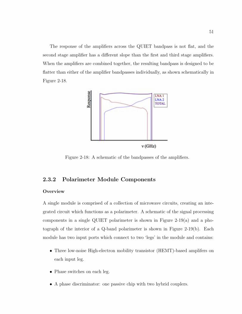
51
The response of the amplifiers across the QUIET bandpass is not flat, and the
second stage amplifier has a different slope than the first and third stage amplifiers.
When the amplifiers are combined together, the resulting bandpass is designed to be
flatter than either of the amplifier bandpasses individually, as shown schematically in
Figure 2-18.
Figure 2-18: A schematic of the bandpasses of the amplifiers.
2.3.2 Polarimeter Module Components
Overview
A single module is comprised of a collection of microwave circuits, creating an inte-
grated circuit which functions as a polarimeter. A schematic of the signal processing
components in a single QUIET polarimeter is shown in Figure 2-19(a) and a pho-
tograph of the interior of a Q-band polarimeter is shown in Figure 2-19(b). Each
module has two input ports which connect to two ‘legs’ in the module and contains:
• Three low-noise High-electron mobility transistor (HEMT)-based amplifers on
each input leg.
• Phase switches on each leg.
• A phase discriminator: one passive chip with two hybrid couplers.
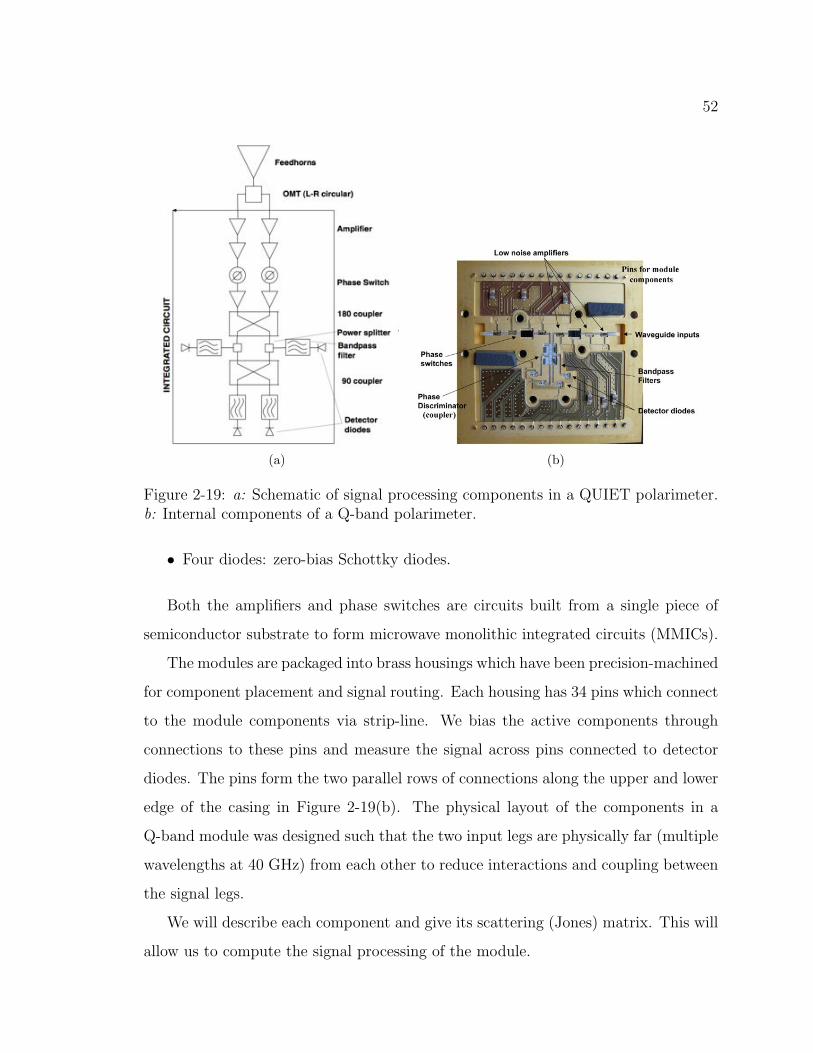
52
(a) (b)
Figure 2-19: a: Schematic of signal processing components in a QUIET polarimeter.b: Internal components of a Q-band polarimeter.
• Four diodes: zero-bias Schottky diodes.
Both the amplifiers and phase switches are circuits built from a single piece of
semiconductor substrate to form microwave monolithic integrated circuits (MMICs).
The modules are packaged into brass housings which have been precision-machined
for component placement and signal routing. Each housing has 34 pins which connect
to the module components via strip-line. We bias the active components through
connections to these pins and measure the signal across pins connected to detector
diodes. The pins form the two parallel rows of connections along the upper and lower
edge of the casing in Figure 2-19(b). The physical layout of the components in a
Q-band module was designed such that the two input legs are physically far (multiple
wavelengths at 40 GHz) from each other to reduce interactions and coupling between
the signal legs.
We will describe each component and give its scattering (Jones) matrix. This will
allow us to compute the signal processing of the module.
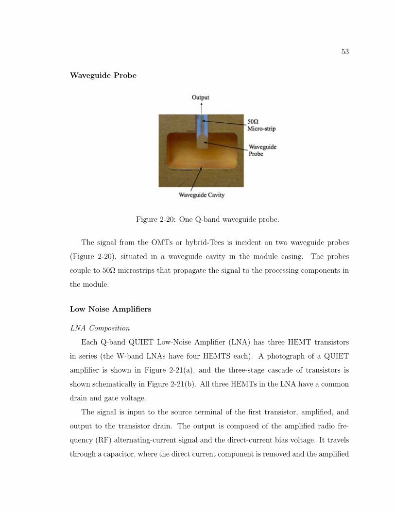
53
Waveguide Probe
Figure 2-20: One Q-band waveguide probe.
The signal from the OMTs or hybrid-Tees is incident on two waveguide probes
(Figure 2-20), situated in a waveguide cavity in the module casing. The probes
couple to 50Ω microstrips that propagate the signal to the processing components in
the module.
Low Noise Amplifiers
LNA Composition
Each Q-band QUIET Low-Noise Amplifier (LNA) has three HEMT transistors
in series (the W-band LNAs have four HEMTS each). A photograph of a QUIET
amplifier is shown in Figure 2-21(a), and the three-stage cascade of transistors is
shown schematically in Figure 2-21(b). All three HEMTs in the LNA have a common
drain and gate voltage.
The signal is input to the source terminal of the first transistor, amplified, and
output to the transistor drain. The output is composed of the amplified radio fre-
quency (RF) alternating-current signal and the direct-current bias voltage. It travels
through a capacitor, where the direct current component is removed and the amplified
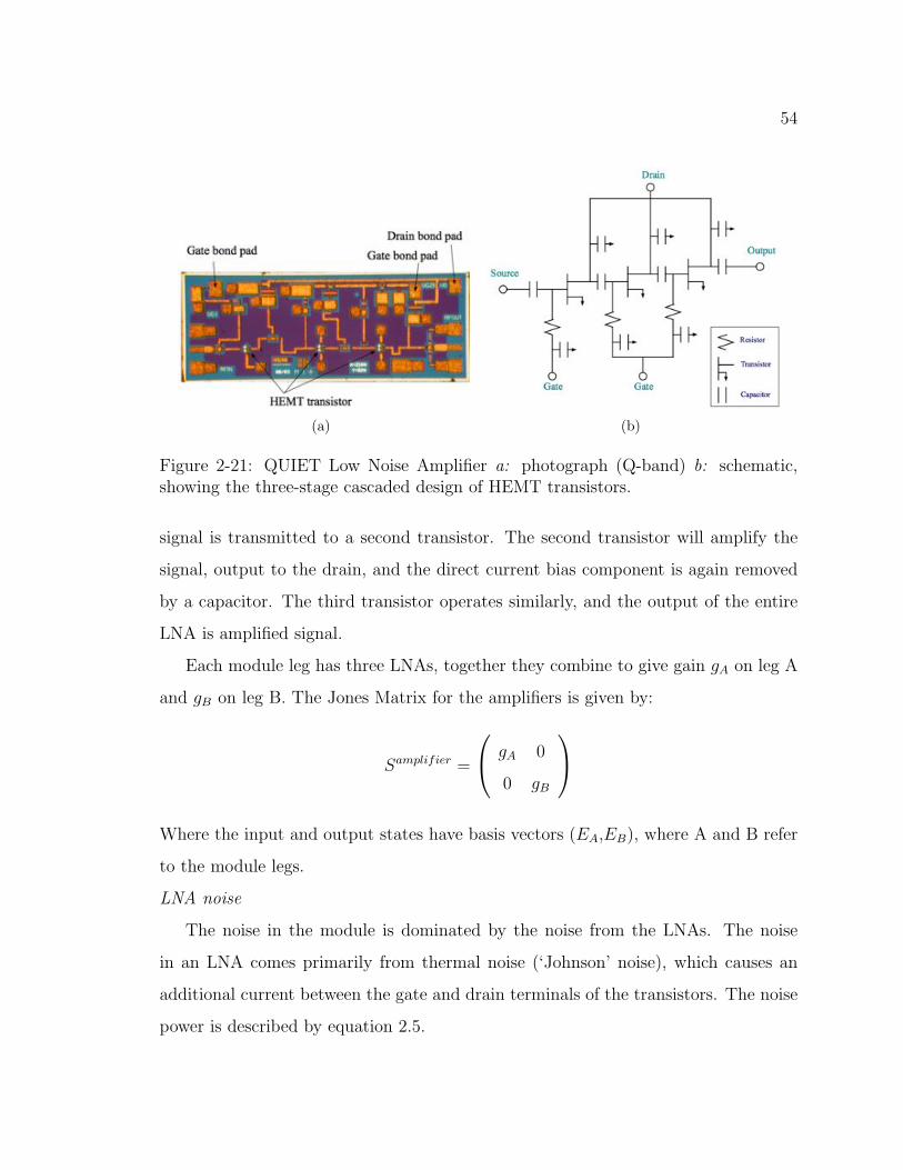
54
(a) (b)
Figure 2-21: QUIET Low Noise Amplifier a: photograph (Q-band) b: schematic,showing the three-stage cascaded design of HEMT transistors.
signal is transmitted to a second transistor. The second transistor will amplify the
signal, output to the drain, and the direct current bias component is again removed
by a capacitor. The third transistor operates similarly, and the output of the entire
LNA is amplified signal.
Each module leg has three LNAs, together they combine to give gain gA on leg A
and gB on leg B. The Jones Matrix for the amplifiers is given by:
Samplifier =
gA 0
0 gB
Where the input and output states have basis vectors (EA,EB), where A and B refer
to the module legs.
LNA noise
The noise in the module is dominated by the noise from the LNAs. The noise
in an LNA comes primarily from thermal noise (‘Johnson’ noise), which causes an
additional current between the gate and drain terminals of the transistors. The noise
power is described by equation 2.5.
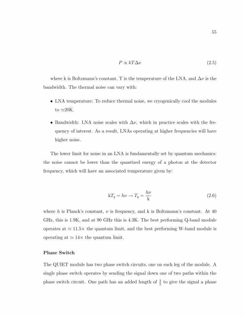
55
P ∝ kT∆ν (2.5)
where k is Boltzmann’s constant, T is the temperature of the LNA, and ∆ν is the
bandwidth. The thermal noise can vary with:
• LNA temperature: To reduce thermal noise, we cryogenically cool the modules
to 20K.
• Bandwidth: LNA noise scales with ∆ν, which in practice scales with the fre-
quency of interest. As a result, LNAs operating at higher frequencies will have
higher noise.
The lower limit for noise in an LNA is fundamentally set by quantum mechanics:
the noise cannot be lower than the quantized energy of a photon at the detector
frequency, which will have an associated temperature given by:
kTq = hν → Tq =hν
k(2.6)
where h is Planck’s constant, ν is frequency, and k is Boltzmann’s constant. At 40
GHz, this is 1.9K, and at 90 GHz this is 4.3K. The best performing Q-band module
operates at 11.5× the quantum limit, and the best performing W-band module is
operating at 14× the quantum limit.
Phase Switch
The QUIET module has two phase switch circuits, one on each leg of the module. A
single phase switch operates by sending the signal down one of two paths within the
phase switch circuit. One path has an added length of λ2
to give the signal a phase
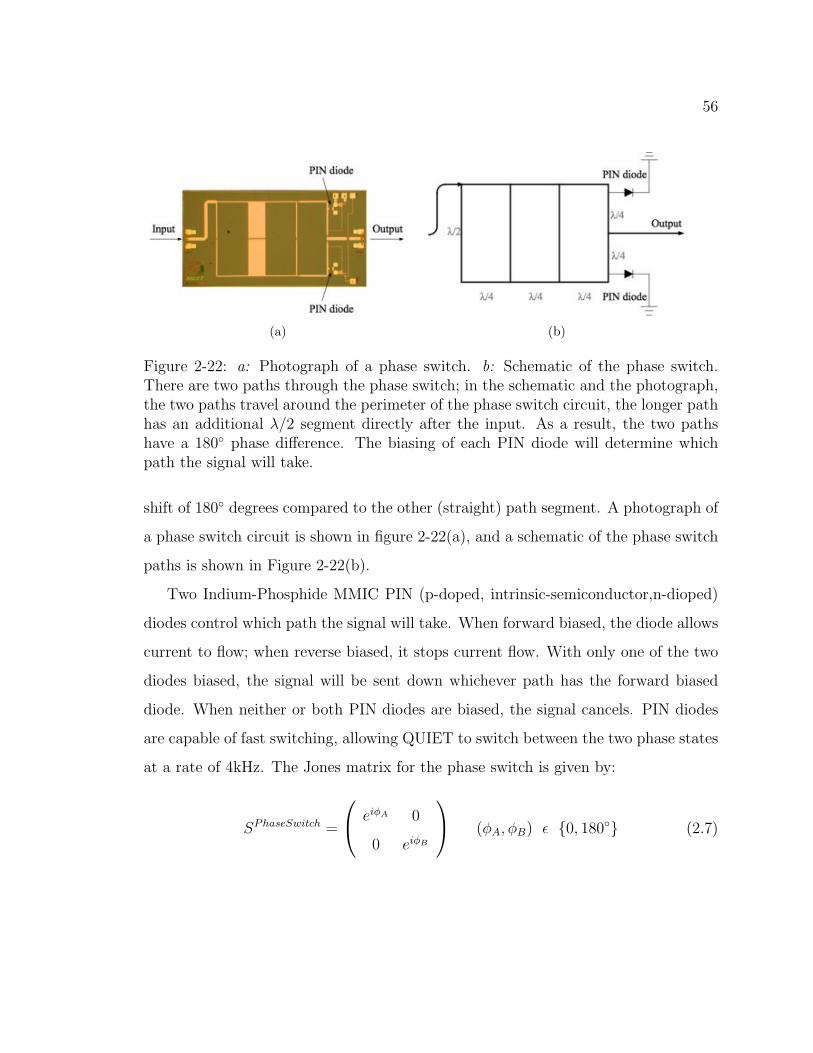
56
(a) (b)
Figure 2-22: a: Photograph of a phase switch. b: Schematic of the phase switch.There are two paths through the phase switch; in the schematic and the photograph,the two paths travel around the perimeter of the phase switch circuit, the longer pathhas an additional λ/2 segment directly after the input. As a result, the two pathshave a 180 phase difference. The biasing of each PIN diode will determine whichpath the signal will take.
shift of 180 degrees compared to the other (straight) path segment. A photograph of
a phase switch circuit is shown in figure 2-22(a), and a schematic of the phase switch
paths is shown in Figure 2-22(b).
Two Indium-Phosphide MMIC PIN (p-doped, intrinsic-semiconductor,n-dioped)
diodes control which path the signal will take. When forward biased, the diode allows
current to flow; when reverse biased, it stops current flow. With only one of the two
diodes biased, the signal will be sent down whichever path has the forward biased
diode. When neither or both PIN diodes are biased, the signal cancels. PIN diodes
are capable of fast switching, allowing QUIET to switch between the two phase states
at a rate of 4kHz. The Jones matrix for the phase switch is given by:
SPhaseSwitch =
eiφA 0
0 eiφB
(φA, φB) 0, 180 (2.7)
57
Phase Discriminator
The phase discriminator consists of two hybrid couplers, each of which is composed of
Schiffman phase delay lines (Ref. [73]) and broadband branchline stripline couplers.
A photograph of a Q-band phase discriminator is shown in Figure 2-23(a), and ac-
companying schematic in Figure 2-23(b). The signal processing of these components
is given in the caption to Figure 2-23(b).
180 coupler
The 180 coupler consists of the Shiffman delay line and coupler shown in the upper
half of Figure 2-23(b), This coupler has a Jones matrix of:
S180
coupler 1√
2
1 1
1 −1
(2.8)
Power Splitter
The output of the 180 coupler is split, and half is sent to a set of detector diodes.
The power splitter has a Jones matrix of:
Spowersplitter =
1√
2
1 0
0 1
(2.9)
90 coupler
The other half of the signal is sent through a phase-delay and coupler structure
identical to the first coupler, shown as the lower half of Figure 2-23(b). The resulting
output is a 90 coupler, with Jones matrix of:
S90
coupler =1√
2
1 i
i 1
(2.10)
This signal is read out by a second set of detector diodes.
58
(a) (b)
Figure 2-23: a: Photograph of a Q-band hybrid coupler or phase discriminator. Theupper half of the photograph shows the 180 coupler composed of Shiffman phasedelay lines and a branchline coupler. The signal is split by a power splitter, and halfof it is read out by a set of detector diodes. The other half of the signal is processedby an identical set of Schiffman phase delay lines and branchline coupler and read outby a second set of detector diodes. Because the input states to this second coupler arethe output of a 180 coupler, it will function as a 90 coupler. The faint horizontaltraces seen in the branchline couplers increase the bandwidth of the coupler. Onepiece of absorber was shifted slightly when the lid of the module was opened. b:
Processing in the hybrid couplers. The first Schiffman phase delay line within thediscriminator will introduce a 3λ
4shift on one module leg, and a λ
2on the other leg,
producing a λ4
phase shift between the legs. Half of the signal on the A leg after theshifter will proceed down the leg, the other half will propagate through the couplingline and will be shifted by λ/4. An identical process will occur for the second leg.Half of the signal on each leg is then split (the square structures in the center of thediagram) and be read by the detector diodes. The signal measured on leg A will be∝A+B while the signal measured on leg B will be ∝A-B. The rest of the signal willpropagate through an identical structure (lower half of the figure), with the resultingsignal described by the output of a 90 coupler.
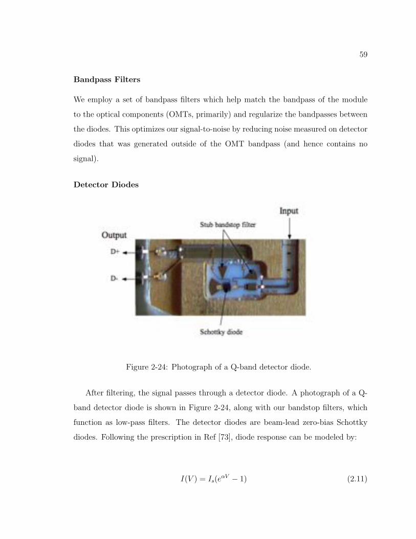
59
Bandpass Filters
We employ a set of bandpass filters which help match the bandpass of the module
to the optical components (OMTs, primarily) and regularize the bandpasses between
the diodes. This optimizes our signal-to-noise by reducing noise measured on detector
diodes that was generated outside of the OMT bandpass (and hence contains no
signal).
Detector Diodes
Figure 2-24: Photograph of a Q-band detector diode.
After filtering, the signal passes through a detector diode. A photograph of a Q-
band detector diode is shown in Figure 2-24, along with our bandstop filters, which
function as low-pass filters. The detector diodes are beam-lead zero-bias Schottky
diodes. Following the prescription in Ref [73], diode response can be modeled by:
I(V ) = Is(eαV− 1) (2.11)
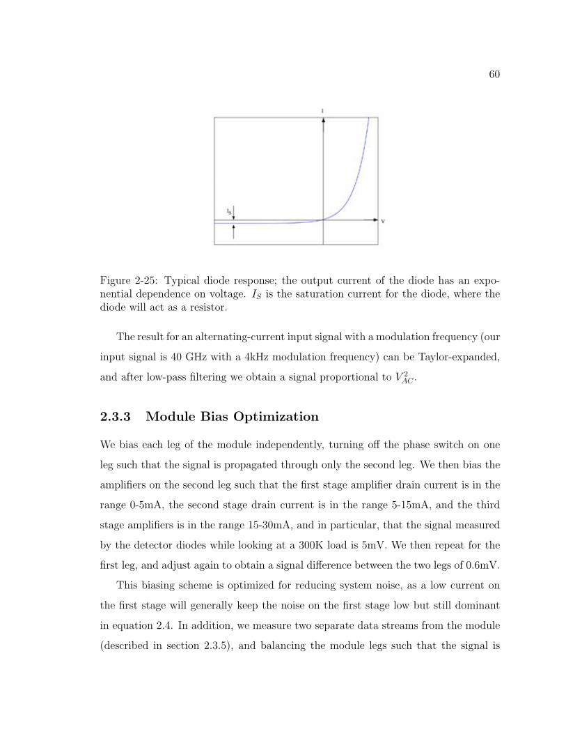
60
Figure 2-25: Typical diode response; the output current of the diode has an expo-nential dependence on voltage. IS is the saturation current for the diode, where thediode will act as a resistor.
The result for an alternating-current input signal with a modulation frequency (our
input signal is 40 GHz with a 4kHz modulation frequency) can be Taylor-expanded,
and after low-pass filtering we obtain a signal proportional to V2
AC .
2.3.3 Module Bias Optimization
We bias each leg of the module independently, turning off the phase switch on one
leg such that the signal is propagated through only the second leg. We then bias the
amplifiers on the second leg such that the first stage amplifier drain current is in the
range 0-5mA, the second stage drain current is in the range 5-15mA, and the third
stage amplifiers is in the range 15-30mA, and in particular, that the signal measured
by the detector diodes while looking at a 300K load is 5mV. We then repeat for the
first leg, and adjust again to obtain a signal difference between the two legs of 0.6mV.
This biasing scheme is optimized for reducing system noise, as a low current on
the first stage will generally keep the noise on the first stage low but still dominant
in equation 2.4. In addition, we measure two separate data streams from the module
(described in section 2.3.5), and balancing the module legs such that the signal is
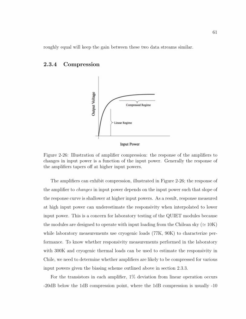
61
roughly equal will keep the gain between these two data streams similar.
2.3.4 Compression
Figure 2-26: Illustration of amplifier compression: the response of the amplifiers tochanges in input power is a function of the input power. Generally the response ofthe amplifiers tapers off at higher input powers.
The amplifiers can exhibit compression, illustrated in Figure 2-26; the response of
the amplifier to changes in input power depends on the input power such that slope of
the response curve is shallower at higher input powers. As a result, response measured
at high input power can underestimate the responsivity when interpolated to lower
input power. This is a concern for laboratory testing of the QUIET modules because
the modules are designed to operate with input loading from the Chilean sky ( 10K)
while laboratory measurements use cryogenic loads (77K, 90K) to characterize per-
formance. To know whether responsivity measurements performed in the laboratory
with 300K and cryogenic thermal loads can be used to estimate the responsivity in
Chile, we need to determine whether amplifiers are likely to be compressed for various
input powers given the biasing scheme outlined above in section 2.3.3.
For the transistors in each amplifier, 1% deviation from linear operation occurs
-20dB below the 1dB compression point, where the 1dB compression is usually -10
62
dB below the bias power; thus compression occurs at -30dB below the bias power
(Ref. [73]). The biasing current is split among the three transistors which compose
an LNA. Typical bias voltages for each amplification stage is given in Table 2.4,
along with the compression point at -30dB from the bias power. With 7dB of loss
between the last amplifier and the diode stage, the condition that the last transistor
in the third amplifier stage is not compressed1 is equivalent to the condition that the
detector diode should measure a signal of -30.5 dB or less. Given the definition:
PdBm = 10× log(Pin
P1mW
) (2.12)
-30.5dB is equivalent to 0.9µW. The detector diodes will output 1mV per 1µW
(Ref. [28]), so the maximum uncompressed signal corresponds to 0.9mV. Thus mea-
sured signals less than 0.9mV are not expected to compress the last transistor in the
third stage amplifier. Biasing the modules such that the detector diode output is 5-
6mV while a module observes the 300K load indicates that we are operating with the
third stage amplifier compressed. Detector diode values while a module observes the
cryogenic loads were 1.3mV, so these may exhibit some compression from the third
stage amplifier. Detector diode values while looking at the Chilean sky (0.3-0.5mV)
indicate the third stage amplifier is uncompressed during observations.
2.3.5 Signal Processing by the QUIET Module
We can combine the Jones matrices of the individual module components to write an
expression for the processing action of the module, independent of the input, for each
of the diodes. We will neglect the filter term as it will simply function as a constant
for each diode. Because we do not combine any of the diodes in the following analysis,
including this factor is unnecessary.
1The other transistors amplify lower input powers, such that this final stage transistor is the onlytransistor near a compression point.
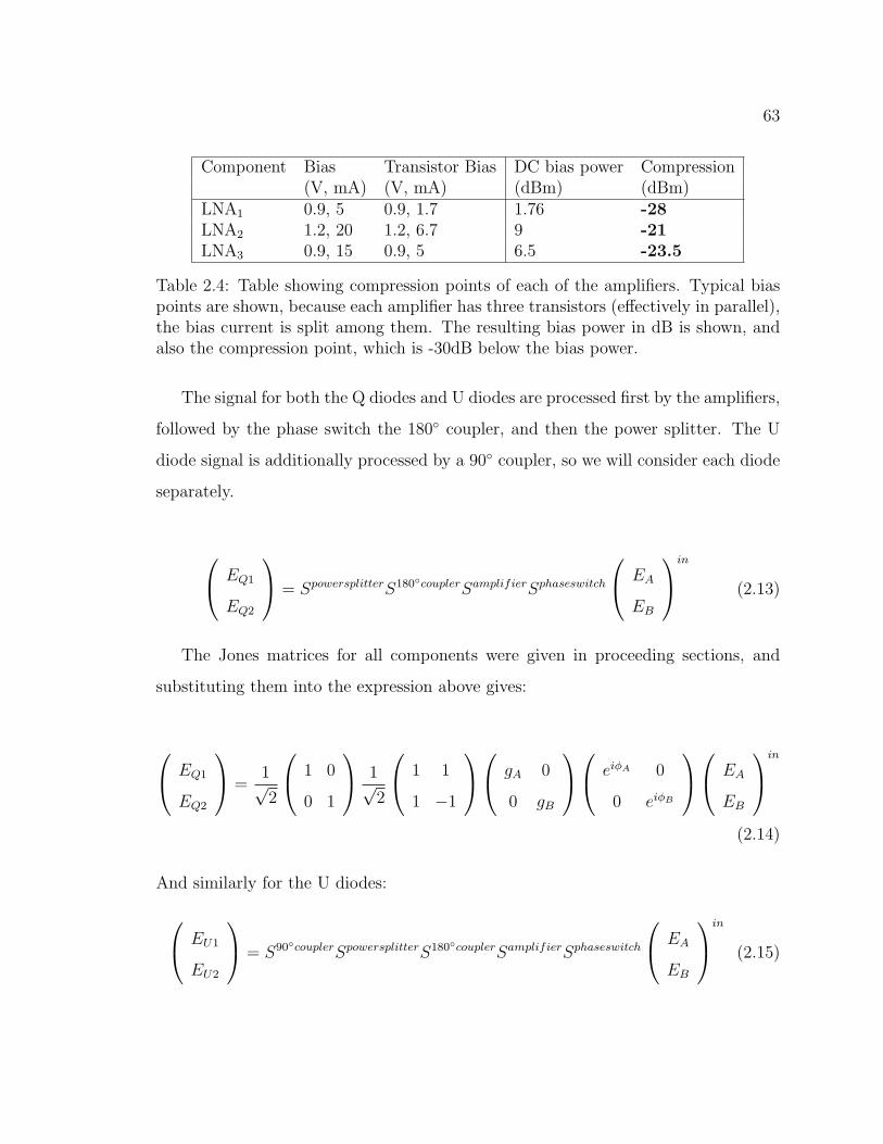
63
Component Bias Transistor Bias DC bias power Compression(V, mA) (V, mA) (dBm) (dBm)
LNA1 0.9, 5 0.9, 1.7 1.76 -28LNA2 1.2, 20 1.2, 6.7 9 -21LNA3 0.9, 15 0.9, 5 6.5 -23.5
Table 2.4: Table showing compression points of each of the amplifiers. Typical biaspoints are shown, because each amplifier has three transistors (effectively in parallel),the bias current is split among them. The resulting bias power in dB is shown, andalso the compression point, which is -30dB below the bias power.
The signal for both the Q diodes and U diodes are processed first by the amplifiers,
followed by the phase switch the 180 coupler, and then the power splitter. The U
diode signal is additionally processed by a 90 coupler, so we will consider each diode
separately.
EQ1
EQ2
= Spowersplitter
S180
couplerS
amplifierS
phaseswitch
EA
EB
in
(2.13)
The Jones matrices for all components were given in proceeding sections, and
substituting them into the expression above gives:
EQ1
EQ2
=1√
2
1 0
0 1
1√
2
1 1
1 −1
gA 0
0 gB
eiφA 0
0 eiφB
EA
EB
in
(2.14)
And similarly for the U diodes:
EU1
EU2
= S90
couplerS
powersplitterS
180coupler
Samplifier
Sphaseswitch
EA
EB
in
(2.15)
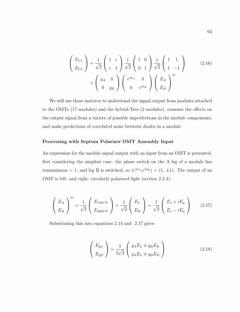
64
EU1
EU2
=1√
2
1 i
i 1
1√
2
1 0
0 1
1√
2
1 1
1 −1
(2.16)
×
gA 0
0 gB
eiφA 0
0 eiφB
EA
EB
in
We will use these matrices to understand the signal output from modules attached
to the OMTs (17 modules) and the hybrid-Tees (2 modules), examine the effects on
the output signal from a variety of possible imperfections in the module components,
and make predictions of correlated noise between diodes in a module.
Processing with Septum Polarizer OMT Assembly Input
An expression for the module signal output with an input from an OMT is presented,
first considering the simplest case: the phase switch on the A leg of a module has
transmission = 1, and leg B is switched, so (eiφA ,eiφB) = (1, ±1). The output of an
OMT is left- and right- circularly polarized light (section 2.2.4):
EA
EB
in
=1√
2
ELHCP
ERHCP
=1√
2
EL
ER
=1√
2
Ex + iEy
Ex − iEy
(2.17)
Substituting this into equations 2.14 and 2.17 gives
EQ1
EQ2
=1
2√
2
gAEL ± gBER
gAEL ∓ gBER
(2.18)
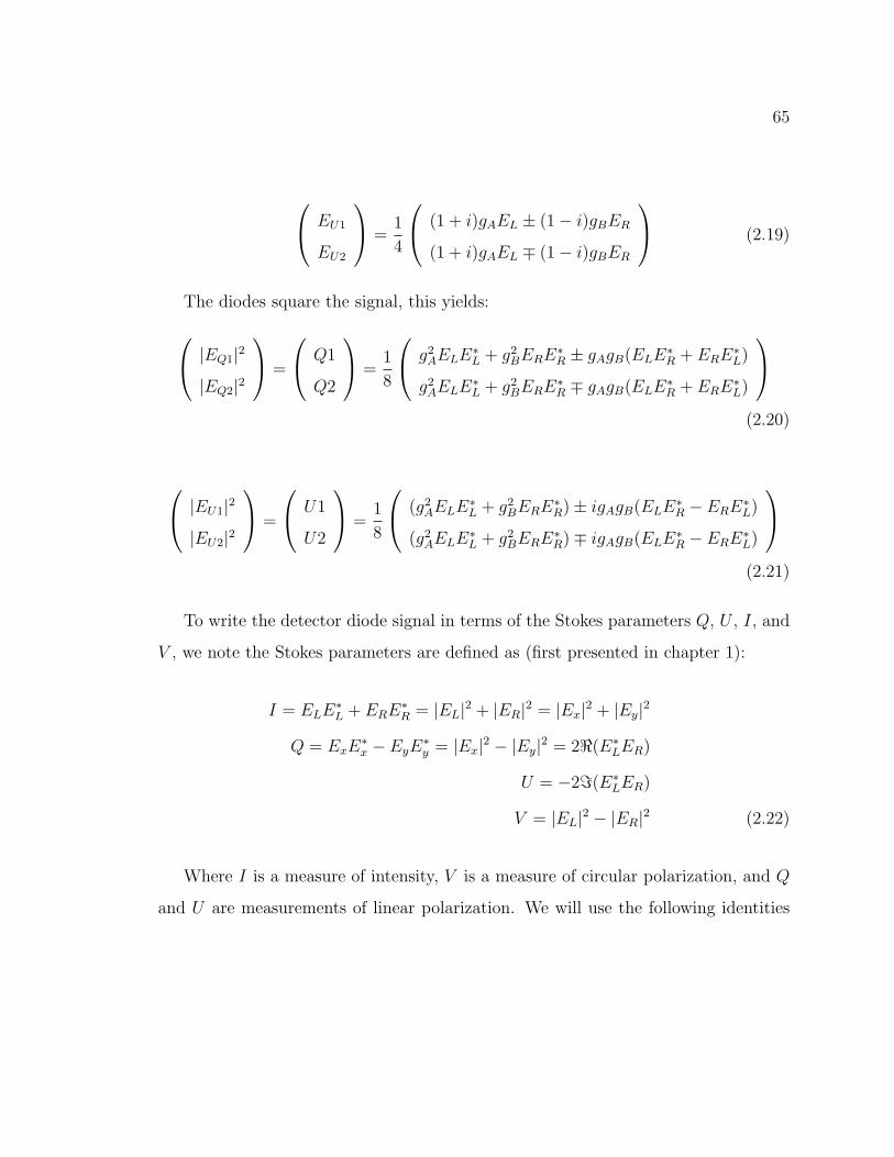
65
EU1
EU2
=1
4
(1 + i)gAEL ± (1− i)gBER
(1 + i)gAEL ∓ (1− i)gBER
(2.19)
The diodes square the signal, this yields:
|EQ1|2
|EQ2|2
=
Q1
Q2
=1
8
g2
AELE∗L + g
2
BERE∗R ± gAgB(ELE
∗R + ERE
∗L)
g2
AELE∗L + g
2
BERE∗R ∓ gAgB(ELE
∗R + ERE
∗L)
(2.20)
|EU1|2
|EU2|2
=
U1
U2
=1
8
(g2
AELE∗L + g
2
BERE∗R) ± igAgB(ELE
∗R − ERE
∗L)
(g2
AELE∗L + g
2
BERE∗R)∓ igAgB(ELE
∗R − ERE
∗L)
(2.21)
To write the detector diode signal in terms of the Stokes parameters Q, U , I, and
V , we note the Stokes parameters are defined as (first presented in chapter 1):
I = ELE∗L + ERE
∗R = |EL|
2 + |ER|2 = |Ex|
2 + |Ey|2
Q = ExE∗x − EyE
∗y = |Ex|
2− |Ey|
2 = 2(E∗LER)
U = −2(E∗LER)
V = |EL|2− |ER|
2 (2.22)
Where I is a measure of intensity, V is a measure of circular polarization, and Q
and U are measurements of linear polarization. We will use the following identities
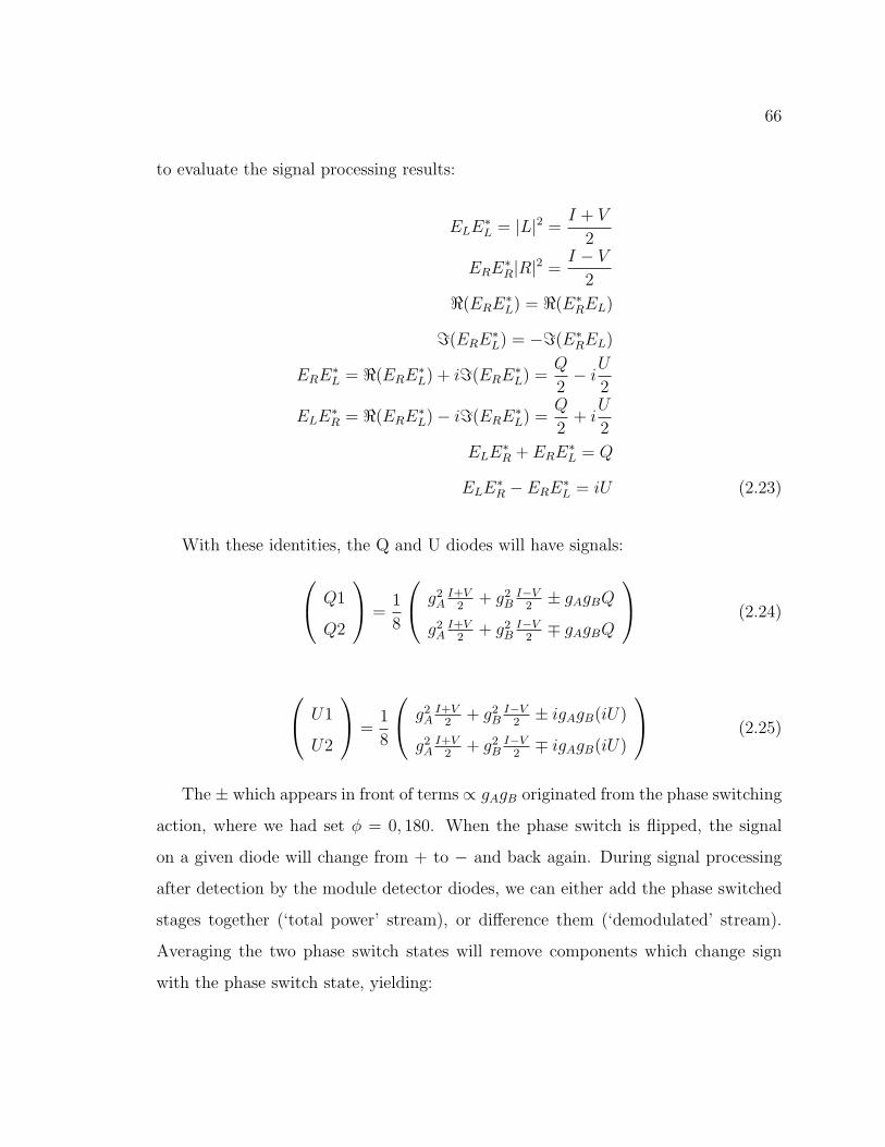
66
to evaluate the signal processing results:
ELE∗L = |L|
2 =I + V
2
ERE∗R|R|
2 =I − V
2
(ERE∗L) = (E∗
REL)
(ERE∗L) = −(E∗
REL)
ERE∗L = (ERE
∗L) + i(ERE
∗L) =
Q
2− i
U
2
ELE∗R = (ERE
∗L)− i(ERE
∗L) =
Q
2+ i
U
2
ELE∗R + ERE
∗L = Q
ELE∗R − ERE
∗L = iU (2.23)
With these identities, the Q and U diodes will have signals:
Q1
Q2
=1
8
g2
AI+V
2+ g
2
BI−V
2± gAgBQ
g2
AI+V
2+ g
2
BI−V
2∓ gAgBQ
(2.24)
U1
U2
=1
8
g2
AI+V
2+ g
2
BI−V
2± igAgB(iU)
g2
AI+V
2+ g
2
BI−V
2∓ igAgB(iU)
(2.25)
The ± which appears in front of terms ∝ gAgB originated from the phase switching
action, where we had set φ = 0, 180. When the phase switch is flipped, the signal
on a given diode will change from + to − and back again. During signal processing
after detection by the module detector diodes, we can either add the phase switched
stages together (‘total power’ stream), or difference them (‘demodulated’ stream).
Averaging the two phase switch states will remove components which change sign
with the phase switch state, yielding:
67
Q1
Q2
total−power
=
U1
U2
total−power
=1
4
(g2
A + g2
B) I2
+ (g2
A − g2
B)V2
(g2
A + g2
B) I2
+ (g2
A − g2
B)V2
(2.26)
Differencing (‘demodulating’) instead removes terms which are constant between
the two phase switch states, yielding:
Q1
Q2
U1
U2
demodulated
=1
4
gAgBQ
−gAgBQ
−gAgBU
gAgBU
(2.27)
The signal on the diodes from modules which are connected to OMTs can be
summarized by:
• The averaged voltage on both the Q and U diodes is a measure of the intensity,
or total power, of the incoming signal. For a black-body emitter such as the
CMB, this is proportional to the temperature.
• The differenced voltage on the Q diodes is a measure of the Q Stokes parameter.
• The differenced voltage on the U diodes is a measure of the U Stokes parameter.
Processing with Hybrid-Tee Assembly Input
As discussed in section 2.2.5, the hybrid-Tee assembly combines the linear polarization
signals from two adjacent horns. Half of the hybrid-Tee assembly outputs the signals
(Ey,1 + Ex,2, Ey,1 - Ex,2) to the input ports of a module, where 1 and 2 refer to the
horn, and x and y are the two linear polarization states. The second half of the
hybrid-Tee assembly outputs (Ey,2 + Ex,1, Ey,2 - Ex,1) to a second module. The signal
output from one half of the hybrid-Tee assembly can be expressed as follows:
68
EA
EB
in
=1√
2
Ey,1 + Ex,2
Ey,1 − Ex,2
(2.28)
The signal output from the diodes is:
Q1
Q2
=
1
8
(g2
A + g2
B)(|Ey,1|2 + |Ex,2|
2) + (g2
A − g2
B)(E∗y,1Ex,2 + Ey,1E
∗x,2)
±2gAgB(|Ey,1|2 − |Ex,2|
2)
(g2
A + g2
B)(|Ey,1|2 + |Ex,2|
2) + (g2
A − g2
B)(E∗y,1Ex,2 + Ey,1E
∗x,2)
∓2gAgB(|Ey,1|2 − |Ex,2|
2)
(2.29)
U1
U2
=1
8
(g2
A + g2
B)(|Ey,1|2 + |Ex,2|
2) + (g2
A − g2
B)(E∗y,1Ex,2 + Ey,1E
∗x,2) ± 0
(g2
A + g2
B)(|Ey,1|2 + |Ex,2|
2) + (g2
A − g2
B)(E∗y,1Ex,2 + Ey,1E
∗x,2)∓ 0
(2.30)
As before, the ± which appears in front of terms ∝ gAgB originated from the
phase switching action. Adding the phase switched stages together will yield ‘total
power’ stream and will remove components which change sign with the phase switch
state::
Q1
Q2
U1
U2
tp,hyb−T
=1
4
(g2
A + g2
B)(|Ey,1|2 + |Ex,2|
2) + (g2
A − g2
B)(E∗y,1Ex,2 + Ey,1E
∗x,2)
(g2
A + g2
B)(|Ey,1|2 + |Ex,2|
2) + (g2
A − g2
B)(E∗y,1Ex,2 + Ey,1E
∗x,2)
(g2
A + g2
B)(|Ey,1|2 + |Ex,2|
2) + (g2
B − g2
A)(E∗y,1Ex,2 + Ey,1E
∗x,2)
(g2
A + g2
B)(|Ey,1|2 + |Ex,2|
2) + (g2
B − g2
A)(E∗y,1Ex,2 + Ey,1E
∗x,2)
(2.31)
Differencing the two phase switch states will yield a ‘demodulated’ stream, con-
69
taining only components which change with the phase switch state:
Q1
Q2
U1
U2
demodulated,hybrid−Tee
=1
4
gAgB(|Ey,1|2 − |Ex,2|
2)
−gAgB(|Ey,1|2 − |Ex,2|
2)
0
0
(2.32)
We will consider the case with gA = gB = 1, which yields a simplified expression
for the expected signals for both of the modules attached to the hybrid-Tee assembly
(denoted as modules 1, 2):
Q1
Q2
total−power,module1
=
U1
U2
total−power,module1
=1
4
(|Ey,1|2 + |Ex,2|
2)
(|Ey,1|2 + |Ex,2|
2)
(2.33)
Q1
Q2
total−power,module2
=
U1
U2
total−power,module2
=1
4
(|Ey,2|2 + |Ex,1|
2)
(|Ey,2|2 + |Ex,1|
2)
(2.34)
Q1
Q2
U1
U2
demodulated,module1
=1
4
(|Ey,1|2 − |Ex,2|
2)
−(|Ey,1|2 − |Ex,2|
2)
0
0
(2.35)
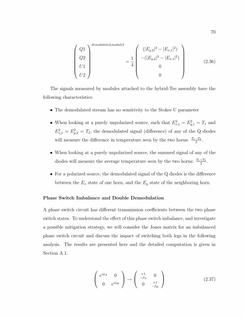
70
Q1
Q2
U1
U2
demodulated,module2
=1
4
(|Ey,2|2 − |Ex,1|
2)
−(|Ey,2|2 − |Ex,1|
2)
0
0
(2.36)
The signals measured by modules attached to the hybrid-Tee assembly have the
following characteristics:
• The demodulated stream has no sensitivity to the Stokes U parameter
• When looking at a purely unpolarized source, such that E2
x,1 = E2
y,1 = T1 and
E2
x,2 = E2
y,2 = T2, the demodulated signal (difference) of any of the Q diodes
will measure the difference in temperature seen by the two horns: T1−T22
.
• When looking at a purely unpolarized source, the summed signal of any of the
diodes will measure the average temperature seen by the two horns: T1+T22
.
• For a polarized source, the demodulated signal of the Q diodes is the difference
between the Ex state of one horn, and the Ey state of the neighboring horn.
Phase Switch Imbalance and Double Demodulation
A phase switch circuit has different transmission coefficients between the two phase
switch states. To understand the effect of this phase switch imbalance, and investigate
a possible mitigation strategy, we will consider the Jones matrix for an imbalanced
phase switch circuit and discuss the impact of switching both legs in the following
analysis. The results are presented here and the detailed computation is given in
Section A.1.
eiφA 0
0 eiφB
→
+1
−βA0
0 +1
−βB
(2.37)
71
Before, we considered eiφA = 1 and e
iφB = ±1. With this new expression for the
phase switching matrix, we have added the following elements:
• We can phase-switch both phase switches, such that eiφA has two possible states
(1, -βA), and similarly for eiφB : (1,-βB).
• The two phase-switch states for each phase switch can have unequal transmis-
sion coefficients. Here we assume the transmission is normalized such that in
one state, a phase-switch will transmit with a coefficient of 1, while in the other
state it transmits with a reduced coefficient of βA,B.
Thus, we have four possible phase-switch states corresponding to: ((1,1),(1,-βB),(-
βA,1),(-βA,-βB)). In section 2.3.5 we held the A leg fixed and switched the B leg; in
this new case the output depends on which phase state of leg A we chose. Thus
phase switching the B leg between 1 and −βB will yield two possible output values,
depending on the phase-switch state of leg A (one for eiφA=1, one for e
iφA = −βA).
Differencing the signal between the two phase switch states on the B leg will yield a
demodulated stream, for two example diodes, of:
(1, 1)− (1,−βB)
(−βA, 1)− (−βA,−βB)
Q1
=1
4
g2
B(1− β2
B)ERE∗R + gAgB(ELE
∗R + ERE
∗L)
g2
B(1− β2
B)ERE∗R + βAgAgB(ELE
∗R + ERE
∗L)
(2.38)
(1, 1)− (1,−βB)
(−βA, 1)− (−βA,−βB)
U1
=1
4
g2
B(1− β2
B)ERE∗R + igAgB(ELE
∗R − ERE
∗L)
g2
B(1− β2
B)ERE∗R − iβAgAgB(ELE
∗R − ERE
∗L)
(2.39)
Without phase switch transmission imbalance, the demodulated stream was pro-
portional to only Stokes Q or U. With phase switch imbalances, the demodulation
72
stream includes the term g2
B(1− β2
B)ERE∗R = g
2
B(1− β2
B)( I−V2
). This represents leak-
age from total power into polarization, and is dependent on the gain in only one leg
(in this case, gB). This is not ideal, we would like the demodulated signal to have no
contributions from total power and depend on the gain from both legs equally. Phase
switching a second time (switching between the two states on leg A: 1 and −βA) and
differencing again (‘double demodulation’) gives:
Q1
Q2
U1
U2
=
1
4
gAgB(1 + βA)(1 + βB)Q
−gAgB(1 + βA)(1 + βB)Q
−gAgB(1 + βA)(1 + βB)U
gAgB(1 + βA)(1 + βB)U
(2.40)
Thus, double demodulation removes the effects of total power leakage, generated
by transmission imbalances in the phase switches.
Module Systematics
We considered a variety of possible systematics which could effect the signal output
of the module. We will use the Jones matrices obtained in previous sections for the
action of each module component, and add a few possible systematics:
• Complex gain in the amplifiers. It is common for the amplifiers to add a phase
contribution to the signal, so we will investigate its effect on the data stream.
• Imperfect input into the 180 coupler. This sort of imperfection could occur if
the coupling leg in the branchline coupler had a slight phase delay. This would
effect the signal processing of both legs.
• Imperfect output from the 180 coupler. This would appear as a phase lag after
the coupler on only one leg.
73
We will investigate these effects with the single-demodulated stream to reduce
algebraic complication, and because double demodulation was meant to remove a
very specific systematic which will not effect the systematics we investigate here.
The full analysis is presented in section A.2, a summary table of the effects of these
imperfections is given in Table 2.5. All of these imperfections will generally cause
a rotation of the Q and U axes, such that the Q and U diodes are not exactly
45 degrees apart from each other. This is consistent with analysis performed on
measurements from calibration observations performed during the observing season
in Chile (section 5.7) which show that the measured detector angles for diodes within
a given module are generally not 45 and 90 apart.
Systematic (Q1,Q2) Demodulated Stream
None ±1
4gAgBQ
Complex gain ±1
4gAgB(Q cos(θ) + U sin(θ))
Phase lag on coupled leg ±1
4gAgB(Q cos(θ)− U sin(θ))
Phase lag on output leg ±1
4gAgBQ, −gAgB(Q cos(θ)− U sin(θ))
(U1, U2) Demodulated Stream
None ±1
4gAgBU
Complex gain ±1
4gAgB(U cos(θ)−Q sin(θ))
Phase lag on coupled leg ±1
4gAgB(U cos(θ) + Q sin(θ))
Phase lag on output leg ∓1
4U(1 + cos(θ) + sin(θ)) + Q(1− cos(θ) + sin(θ))
Averaged Stream
None 1
4((g2
A + g2
B) I2
+ (g2
A − g2
B)V2)
Complex gain 1
4((g2
A + g2
B) I2
+ (g2
A − g2
B)V2)
Phase lag on coupled leg 1
4((g2
A + g2
B) I2
+ (g2
A − g2
B)V2)
Phase lag on output leg 1
4((g2
A + g2
B[1 + sin(θ)] I2
+ (g2
A − g2
B[1 + sin(θ)])V2)
(Q1,Q2) hybrid-Tee Demodulated Stream
None ±1
4gAgB(|Ey,1|
2 − |Ex,2|2)
Phase lag on input leg ±1
4gAgB([|Ey,1|
2 − |Ex,2|2] cos(θ) + [E∗
y,1Ex,2 − Ey,1E∗x,2] sin(θ))
(U1,U2) hybrid-Tee Demodulated Stream
None 0Phase lag on input leg ±
1
4gAgB([|Ey,1|
2 − |Ex,2|2] sin(θ) + [E∗
y,1Ex,2 − Ey,1E∗x,2] cos(θ))
(all diodes) Hybrid-Tee Average Stream
None 1
4(g2
A + g2
B)(|Ey,1|2 + |Ex,2|
2) + (g2
A − g2
B)(E∗y,1Ex,2 + Ey,1E∗
x,2)Phase lag on input leg 1
4(g2
A + g2
B)(|Ey,1|2 + |Ex,2|
2) + (g2
A − g2
B)(E∗y,1Ex,2 + Ey,1E∗
x,2)
Table 2.5: Summary of possible systematics with their effects on the demodulatedand averaged streams, as well as the hybrid-Tee modules.
74
Correlated Noise
We investigate the effects of correlated noise in a module. This analysis was presented
in Ref. [8].
We express EL = a0 + ia1 and ER = b0 + ib1, and assume the variables a0,a1,b0,b1
are Gaussian random, and that a0 and a1 are drawn from the same distribution, but
a different distribution from b0 and b1. As Gaussian variables, they have the following
properties:
< a2
0>=< a
2
1>= σ
2
a
< b2
0>=< b
2
1>= σ
2
b
(2.41)
Basic Correlation
The correlation expression we use is a standard correlation coefficient (Ref. [63]),
given by:
CXY =< XY > − < X >< Y >
(< X2 > − < X >2)(< Y 2 > − < Y >2)(2.42)
In this case, X is the TOD for one diode (Q1, Q2, U1 or U2), and Y is the
TOD for the second diode under consideration (also one of Q1, Q2, U1, or U2). The
correlations for the various systematics considered above are given in Table 2.6 and
the computation is presented in Section A.4.
We found that:
• For a case with no systematics where the gain and noise are equal in the two
legs, the Q diodes should be uncorrelated with each other, the U diodes should
be uncorrelated with each other, and all pairs of Q and U diodes (Q1U1, Q1U2,
Q2U1, Q2U2) should be correlated with a coefficient of 0.5.
75
• Introducing complex gain or a phase lag in the input to the coupler does not
result in additional correlated noise.
• In the case where there is a lag at the output of the 180 hybrid, there is
increased correlation between the diode pairs.
We compute this correlation coefficient for each scan in the observing season (this
processing will be discussed in chapter 6). We find each module has some additional
correlated noise, a few modules have correlation coefficients in excess by as much
as 0.3, which may be pointing to a non-ideality in the output of the coupler. We
include noise correlation coefficients in the analysis pipelines, this will be discussed
in chapter 6.
76
Syst
emati
c(Q
1-Q
2)
(U1-U
2)
Q-U
Non
e(g2 A
σ2 a−
g2 B
σ2 b)2
(g2 A
σ2 a+
g2 B
σ2 b)2
g A=
g B,σ
a=
σb
→0
(g2 A
σ2 a−
g2 B
σ2 b)2
(g2 A
σ2 a+
g2 B
σ2 b)2
g A=
g B,σ
a=
σb
→0
(g4 A
σ4 a+
g4 B
σ4 b)
(g2 A
σ2 a+
g2 B
σ2 b)2
g A=
g B,σ
a=
σb
→0.
5
Com
ple
xga
in(g2 A
σ2 a−
g2 B
σ2 b)2
(g2 A
σ2 a+
g2 B
σ2 b)2
g A=
g B,σ
a=
σb
→0
(g2 A
σ2 a−
g2 B
σ2 b)2
(g2 A
σ2 a+
g2 B
σ2 b)2
g A=
g B,σ
a=
σb
→0
(g4 A
σ4 a+
g4 B
σ4 b)
(g2 A
σ2 a+
g2 B
σ2 b)2
g A=
g B,σ
a=
σb
→0.
5
Phas
ela
gon
couple
dle
g(g2 A
σ2 a−
g2 B
σ2 b)2
(g2 A
σ2 a+
g2 B
σ2 b)2
g A=
g B,σ
a=
σb
→0
(g2 A
σ2 a−
g2 B
σ2 b)2
(g2 A
σ2 a+
g2 B
σ2 b)2
g A=
g B,σ
a=
σb
→0
(g4 A
σ4 a+
g4 B
σ4 b)
(g2 A
σ2 a+
g2 B
σ2 b)2
g A=
g B,σ
a=
σb
→0.
5
Phas
ela
gon
outp
ut
leg
σ4 a−
2σ
2 aσ
2 bcos(θ)
+σ
4 b
(σ
2 a+
σ2 b)2
→0
(g2 A
σ2 a−
g2 B
σ2 bcosθ)
2
(g2 A
σ4 a+
2g a
g bσ
2 aσ
2 b+
σ4 bcos2(θ)
)→
0σ
4 a+
σ2 aσ
2 b[1−
cos(θ)
+sin
(θ)
]+σ
4 b[1
+sin
(θ)
]
(σ
4 a+
σ2 aσ
2 b(2+
sin
(θ)
)+
σ2 b[1
+sin
(θ)
])2→
0.5
Tab
le2.
6:Sum
mar
yof
corr
elat
ion
coeffi
cien
ts,in
cludin
gth
esy
stem
atic
sst
udie
s.B
ecau
seQ
1an
dQ
2diff
erby
only
asi
gn,an
dU
1an
dU
2diff
erby
only
asi
gn,th
eco
rrel
atio
nex
pre
ssio
nis
iden
tica
lbet
wee
nal
lQ
-Upai
rs,su
chth
atin
this
table
Q-U
den
otes
Q1U
1,Q
1U2,
Q2U
1,an
dQ
2U2.
The
only
case
whic
hin
trod
uce
dad
ditio
nal
corr
elat
ion
was
the
case
wit
ha
phas
ela
gon
the
outp
ut
leg.
77
2.4 Single Module Testing at the Jet Propulsion
Laboratory and Columbia University
We measured bandpasses and intrinsic module noise for each module individually
in test cryostats both at the Jet Propulsion laboratory and at Columbia University.
The cryostat used for testing at Columbia was designed to closely mimic the Q-band
receiver; it contains a single feedhorn similar to the Q-band feedhorns, an OMT of
nearly the same design we use in the receiver, and a small window prepared identically
to the Q-band receiver window (see section 2.6.5). This allowed us to perform tests
which were also similar to tests performed with the receiver array, the results of which
we could use to predict the end-to-end performance of the receiver.
Bandpasses are measured by injecting a frequency-swept input signal into the
module through the window of the test cryostat. The polarized frequency-swept
input signal allows us to measure the module response as a function of frequency,
and compute module bandwidth and central frequency (these equations, and the
measurements with the array, are described in section 3.2). Two small cryogenic
thermal loads were used to assess the module noise with this setup, they were built
identically to the large thermal loads used for noise tests with the receiver. Measuring
the module response for each of two thermal loads at a known temperature allows us
to extract module noise temperature (this is outlined in detail in section 3.3).
To achieve QUIET science goals, we required that each module have a noise tem-
perature less than 35K and a bandwidth greater than 7.5GHz (these criteria are
described in section 3.3). The single-module tests were used to evaluate whether or
not a module should be included: if each diode in the module met these criteria in
the test setup, then the module was included in the array. Ultimately we did not
compare values for these quantities obtained in the testing setup and the receiver as
differences are more likely attributable to the differences two setups than changes in
module performance: the OMT in the single-module test cryostat has a slightly dif-

78
ferent central frequency and the amplifier biasing is very different from the electronics
boards used for the receiver.

79
2.5 QUIET Electronics
2.5.1 Introduction
This section will discuss the electronics boards, weather-proofing, enclosure system,
and the cabling scheme in the QUIET experiment. The electronics boards are com-
prised of:
• Protection circuitry: protect the QUIET modules from voltage spiking.
– Module Attachment Board
– Array Interface Board
• Bias Circuitry: provide bias voltage to QUIET module components (section 2.3.2).
– Amplifier Bias Boards
– Phase-Switch Bias Boards
– Pre-amplifier Boards (detector diode bias)
• Analog-to-digital conversion: The Analog-digital conversion (ADC) boards con-
tain ADC chips (AD7674) which convert analog signals from the module detec-
tor diodes to a digital signal readable by a control computer. The master ADC
has the additional task of relaying biasing commands and timing signals to the
other boards.
• Housekeeping Board: monitor amplifier and phase switch bias voltages and
currents as well as cryostat temperatures.
• Timing Card and Auxiliary Timing Card: provide a timing signal to the master
ADC that is synchronized to the telescope timing.
• External-temperature Monitor Boards: monitor the temperature of the mirrors
and ground screen.
80
The quantity of each type of board for the Q- and W-band instruments, and the
number of modules each board-type can support, is given in Table 2.7.
2.5.2 Electronics Overview
Figure 2-27: A simplified schematic of the QUIET Q-band electronics. Shown arethe boards described in the text: the ADC boards (master and two slaves), twotiming cards, crate computer, and ADC backplane. Also shown are the bias boards,housekeeping board, and bias-board backplane. These boards are all located withinan electronics enclosure. The Array Interface Boards are housed separately, and theModule Attachment Boards are located within the cryostat.
Figure 2-27 shows a simplified diagram and connection scheme for the electronics
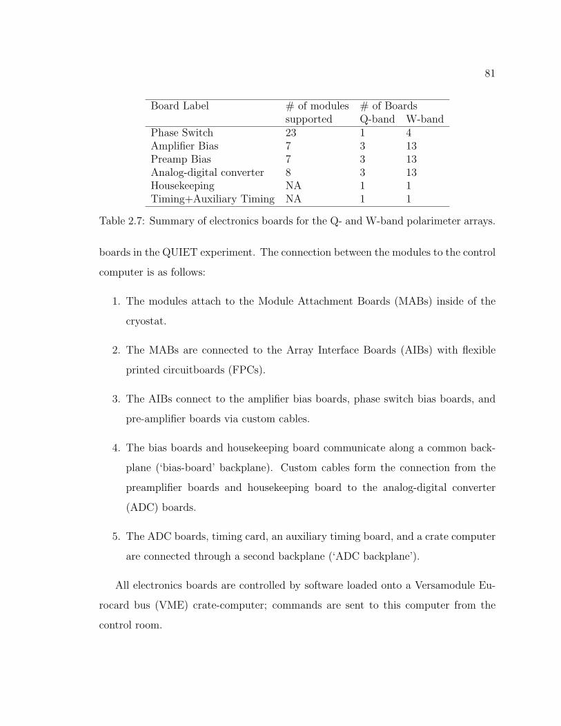
81
Board Label # of modules # of Boardssupported Q-band W-band
Phase Switch 23 1 4Amplifier Bias 7 3 13Preamp Bias 7 3 13Analog-digital converter 8 3 13Housekeeping NA 1 1Timing+Auxiliary Timing NA 1 1
Table 2.7: Summary of electronics boards for the Q- and W-band polarimeter arrays.
boards in the QUIET experiment. The connection between the modules to the control
computer is as follows:
1. The modules attach to the Module Attachment Boards (MABs) inside of the
cryostat.
2. The MABs are connected to the Array Interface Boards (AIBs) with flexible
printed circuitboards (FPCs).
3. The AIBs connect to the amplifier bias boards, phase switch bias boards, and
pre-amplifier boards via custom cables.
4. The bias boards and housekeeping board communicate along a common back-
plane (‘bias-board’ backplane). Custom cables form the connection from the
preamplifier boards and housekeeping board to the analog-digital converter
(ADC) boards.
5. The ADC boards, timing card, an auxiliary timing board, and a crate computer
are connected through a second backplane (‘ADC backplane’).
All electronics boards are controlled by software loaded onto a Versamodule Eu-
rocard bus (VME) crate-computer; commands are sent to this computer from the
control room.
82
Electronics Enclosures
The backplanes, bias boards, ADC boards, timing cards, external temperature mon-
itor boards, and crate computer are all housed in a thermally-regulated electronics
enclosure. The enclosure is water- and weather-proof, protecting the electronics from
the harsh conditions of the Chilean desert and serving as a Faraday cage to minimize
radio-frequency interference, which can introduce unwanted spikes in the science data
signal. The enclosure also supports a set of linear power supplies – which power the
bias boards – and regulation circuits for controlling the cryostat temperatures and
the enclosure temperatures.
The temperature of the electronics enclosure is regulated at 25C and and is set
to control the temperature to ±1C. The enclosure temperature during the Q-band
observing season is shown in Figure 2-28 for one of the enclosure temperature sensors.
This sensor has an average value of 25.4C with root-mean-square (RMS) of ±1.1C
(these sensors are not absolutely calibrated, so while we regulate to 25C, the sensor
will have offset – in this case 0.5C). There was a downward linear trend in enclosure
temperature over the course of the season, dropping by 1 over the entire season.
This is not correlated with ambient temperature and the cause is unknown. The large
deviations in temperature occurred when regulation failed, this represents 10% of
the full data set.
Cabling and Backplanes
Each module requires 25 independent wires to bias the active components and read
the signals from the detector diodes. The 19 modules in the Q-band array require
a total of 500 bias and signal connections (the W-band array will require 5×
more connections), which must be made through a hermetic seal. To keep the cabling
manageable within the cryostat, QUIET opted to use flexible printed circuit boards
(FPCs), depicted in Figure 2-29, to make the connection between the MABs and the
AIBs. FPCs have extremely high-density traces, necessary for the number of bias
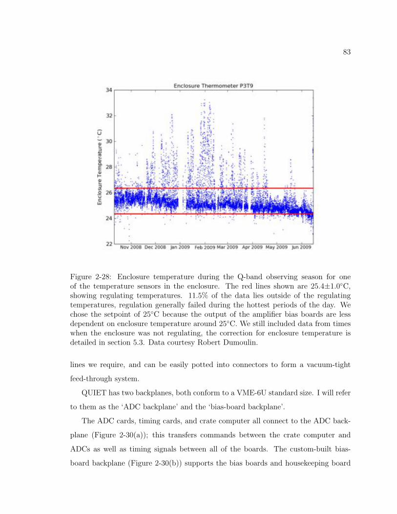
83
Figure 2-28: Enclosure temperature during the Q-band observing season for oneof the temperature sensors in the enclosure. The red lines shown are 25.4±1.0C,showing regulating temperatures. 11.5% of the data lies outside of the regulatingtemperatures, regulation generally failed during the hottest periods of the day. Wechose the setpoint of 25C because the output of the amplifier bias boards are lessdependent on enclosure temperature around 25C. We still included data from timeswhen the enclosure was not regulating, the correction for enclosure temperature isdetailed in section 5.3. Data courtesy Robert Dumoulin.
lines we require, and can be easily potted into connectors to form a vacuum-tight
feed-through system.
QUIET has two backplanes, both conform to a VME-6U standard size. I will refer
to them as the ‘ADC backplane’ and the ‘bias-board backplane’.
The ADC cards, timing cards, and crate computer all connect to the ADC back-
plane (Figure 2-30(a)); this transfers commands between the crate computer and
ADCs as well as timing signals between all of the boards. The custom-built bias-
board backplane (Figure 2-30(b)) supports the bias boards and housekeeping board
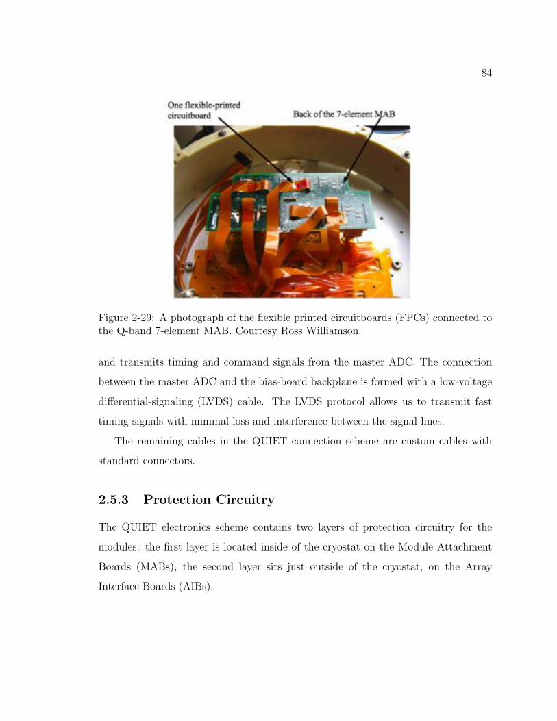
84
Figure 2-29: A photograph of the flexible printed circuitboards (FPCs) connected tothe Q-band 7-element MAB. Courtesy Ross Williamson.
and transmits timing and command signals from the master ADC. The connection
between the master ADC and the bias-board backplane is formed with a low-voltage
differential-signaling (LVDS) cable. The LVDS protocol allows us to transmit fast
timing signals with minimal loss and interference between the signal lines.
The remaining cables in the QUIET connection scheme are custom cables with
standard connectors.
2.5.3 Protection Circuitry
The QUIET electronics scheme contains two layers of protection circuitry for the
modules: the first layer is located inside of the cryostat on the Module Attachment
Boards (MABs), the second layer sits just outside of the cryostat, on the Array
Interface Boards (AIBs).
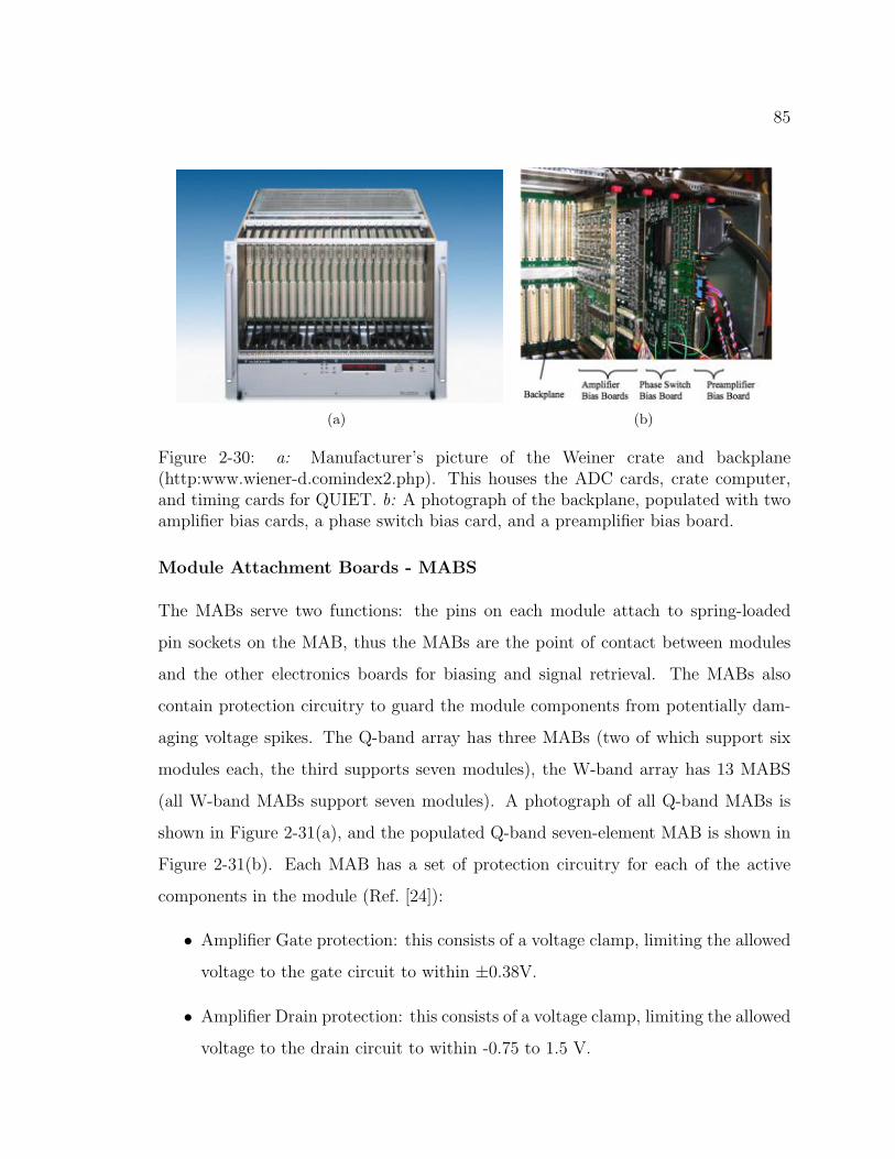
85
(a) (b)
Figure 2-30: a: Manufacturer’s picture of the Weiner crate and backplane(http:www.wiener-d.comindex2.php). This houses the ADC cards, crate computer,and timing cards for QUIET. b: A photograph of the backplane, populated with twoamplifier bias cards, a phase switch bias card, and a preamplifier bias board.
Module Attachment Boards - MABS
The MABs serve two functions: the pins on each module attach to spring-loaded
pin sockets on the MAB, thus the MABs are the point of contact between modules
and the other electronics boards for biasing and signal retrieval. The MABs also
contain protection circuitry to guard the module components from potentially dam-
aging voltage spikes. The Q-band array has three MABs (two of which support six
modules each, the third supports seven modules), the W-band array has 13 MABS
(all W-band MABs support seven modules). A photograph of all Q-band MABs is
shown in Figure 2-31(a), and the populated Q-band seven-element MAB is shown in
Figure 2-31(b). Each MAB has a set of protection circuitry for each of the active
components in the module (Ref. [24]):
• Amplifier Gate protection: this consists of a voltage clamp, limiting the allowed
voltage to the gate circuit to within ±0.38V.
• Amplifier Drain protection: this consists of a voltage clamp, limiting the allowed
voltage to the drain circuit to within -0.75 to 1.5 V.
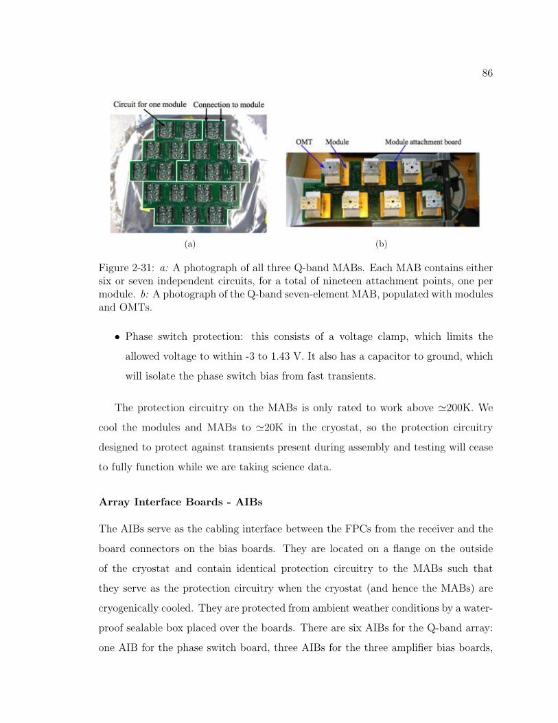
86
(a) (b)
Figure 2-31: a: A photograph of all three Q-band MABs. Each MAB contains eithersix or seven independent circuits, for a total of nineteen attachment points, one permodule. b: A photograph of the Q-band seven-element MAB, populated with modulesand OMTs.
• Phase switch protection: this consists of a voltage clamp, which limits the
allowed voltage to within -3 to 1.43 V. It also has a capacitor to ground, which
will isolate the phase switch bias from fast transients.
The protection circuitry on the MABs is only rated to work above 200K. We
cool the modules and MABs to 20K in the cryostat, so the protection circuitry
designed to protect against transients present during assembly and testing will cease
to fully function while we are taking science data.
Array Interface Boards - AIBs
The AIBs serve as the cabling interface between the FPCs from the receiver and the
board connectors on the bias boards. They are located on a flange on the outside
of the cryostat and contain identical protection circuitry to the MABs such that
they serve as the protection circuitry when the cryostat (and hence the MABs) are
cryogenically cooled. They are protected from ambient weather conditions by a water-
proof sealable box placed over the boards. There are six AIBs for the Q-band array:
one AIB for the phase switch board, three AIBs for the three amplifier bias boards,

87
and two AIBs for the three preamp boards.
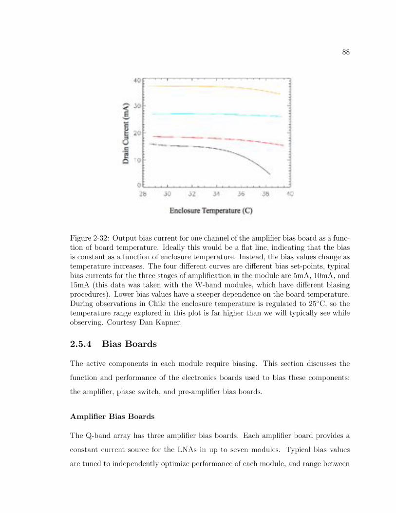
88
Figure 2-32: Output bias current for one channel of the amplifier bias board as a func-tion of board temperature. Ideally this would be a flat line, indicating that the biasis constant as a function of enclosure temperature. Instead, the bias values change astemperature increases. The four different curves are different bias set-points, typicalbias currents for the three stages of amplification in the module are 5mA, 10mA, and15mA (this data was taken with the W-band modules, which have different biasingprocedures). Lower bias values have a steeper dependence on the board temperature.During observations in Chile the enclosure temperature is regulated to 25C, so thetemperature range explored in this plot is far higher than we will typically see whileobserving. Courtesy Dan Kapner.
2.5.4 Bias Boards
The active components in each module require biasing. This section discusses the
function and performance of the electronics boards used to bias these components:
the amplifier, phase switch, and pre-amplifier bias boards.
Amplifier Bias Boards
The Q-band array has three amplifier bias boards. Each amplifier board provides a
constant current source for the LNAs in up to seven modules. Typical bias values
are tuned to independently optimize performance of each module, and range between
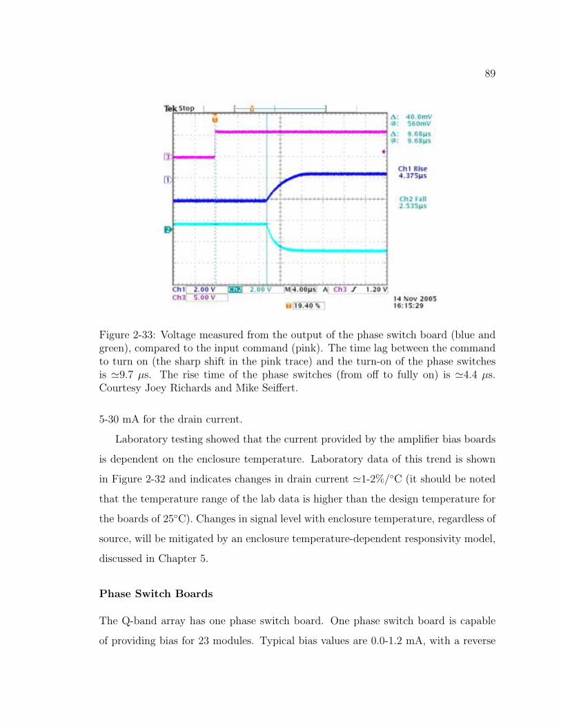
89
Figure 2-33: Voltage measured from the output of the phase switch board (blue andgreen), compared to the input command (pink). The time lag between the commandto turn on (the sharp shift in the pink trace) and the turn-on of the phase switchesis 9.7 µs. The rise time of the phase switches (from off to fully on) is 4.4 µs.Courtesy Joey Richards and Mike Seiffert.
5-30 mA for the drain current.
Laboratory testing showed that the current provided by the amplifier bias boards
is dependent on the enclosure temperature. Laboratory data of this trend is shown
in Figure 2-32 and indicates changes in drain current 1-2%/C (it should be noted
that the temperature range of the lab data is higher than the design temperature for
the boards of 25C). Changes in signal level with enclosure temperature, regardless of
source, will be mitigated by an enclosure temperature-dependent responsivity model,
discussed in Chapter 5.
Phase Switch Boards
The Q-band array has one phase switch board. One phase switch board is capable
of providing bias for 23 modules. Typical bias values are 0.0-1.2 mA, with a reverse
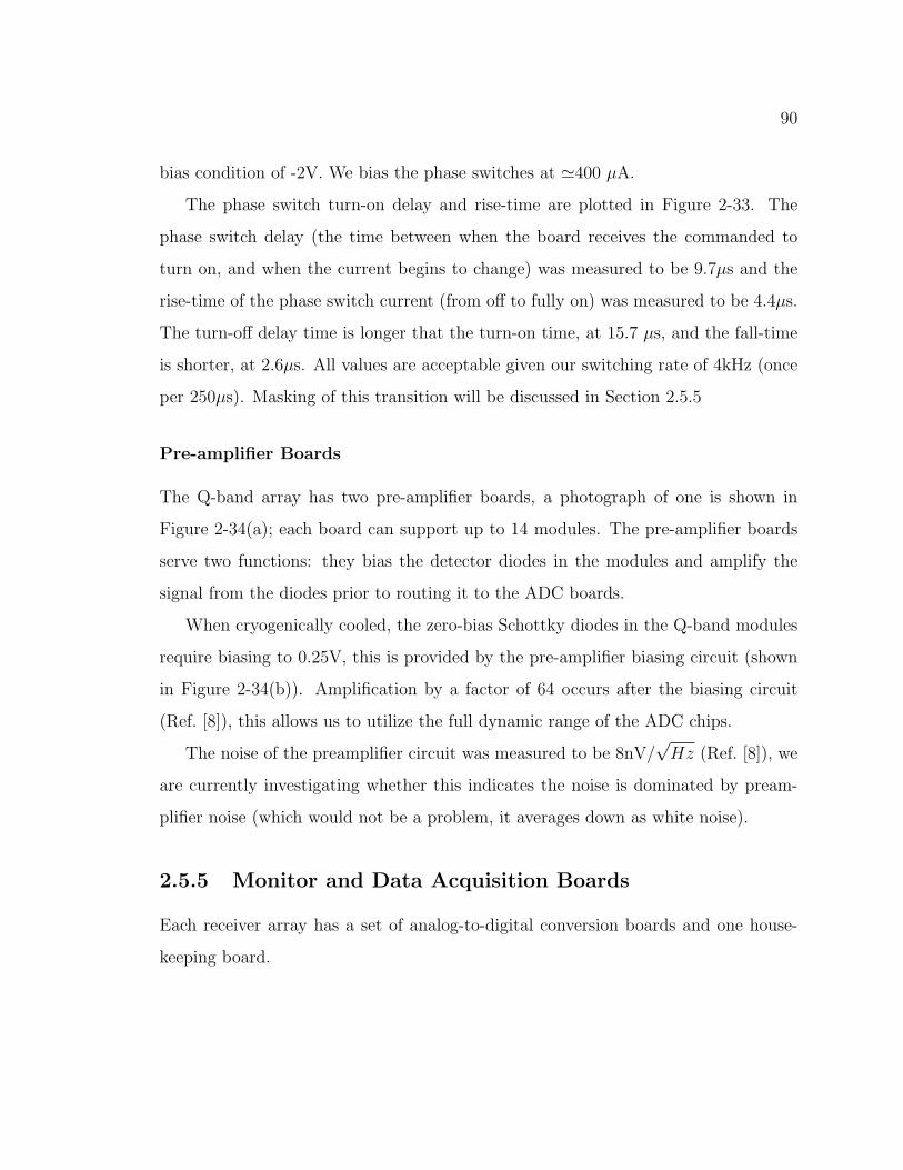
90
bias condition of -2V. We bias the phase switches at 400 µA.
The phase switch turn-on delay and rise-time are plotted in Figure 2-33. The
phase switch delay (the time between when the board receives the commanded to
turn on, and when the current begins to change) was measured to be 9.7µs and the
rise-time of the phase switch current (from off to fully on) was measured to be 4.4µs.
The turn-off delay time is longer that the turn-on time, at 15.7 µs, and the fall-time
is shorter, at 2.6µs. All values are acceptable given our switching rate of 4kHz (once
per 250µs). Masking of this transition will be discussed in Section 2.5.5
Pre-amplifier Boards
The Q-band array has two pre-amplifier boards, a photograph of one is shown in
Figure 2-34(a); each board can support up to 14 modules. The pre-amplifier boards
serve two functions: they bias the detector diodes in the modules and amplify the
signal from the diodes prior to routing it to the ADC boards.
When cryogenically cooled, the zero-bias Schottky diodes in the Q-band modules
require biasing to 0.25V, this is provided by the pre-amplifier biasing circuit (shown
in Figure 2-34(b)). Amplification by a factor of 64 occurs after the biasing circuit
(Ref. [8]), this allows us to utilize the full dynamic range of the ADC chips.
The noise of the preamplifier circuit was measured to be 8nV/√
Hz (Ref. [8]), we
are currently investigating whether this indicates the noise is dominated by pream-
plifier noise (which would not be a problem, it averages down as white noise).
2.5.5 Monitor and Data Acquisition Boards
Each receiver array has a set of analog-to-digital conversion boards and one house-
keeping board.
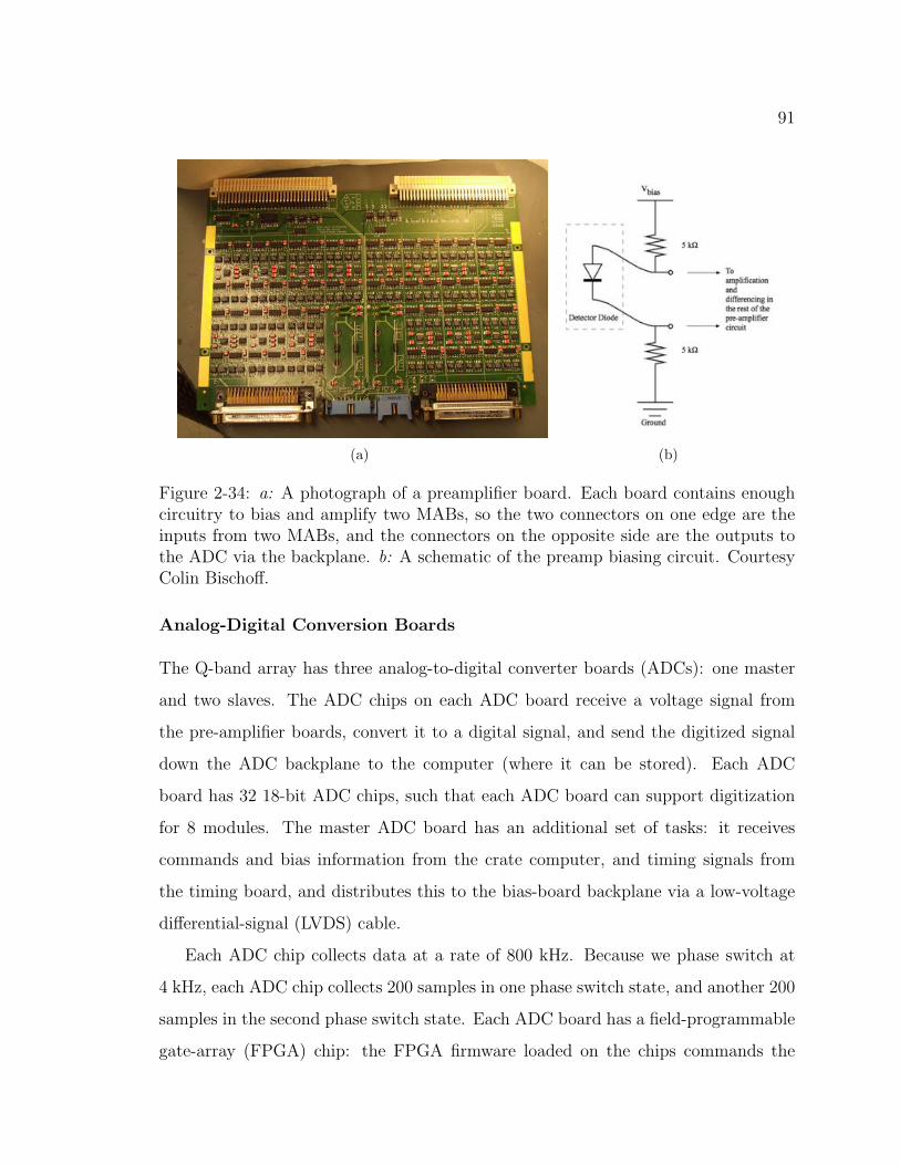
91
(a) (b)
Figure 2-34: a: A photograph of a preamplifier board. Each board contains enoughcircuitry to bias and amplify two MABs, so the two connectors on one edge are theinputs from two MABs, and the connectors on the opposite side are the outputs tothe ADC via the backplane. b: A schematic of the preamp biasing circuit. CourtesyColin Bischoff.
Analog-Digital Conversion Boards
The Q-band array has three analog-to-digital converter boards (ADCs): one master
and two slaves. The ADC chips on each ADC board receive a voltage signal from
the pre-amplifier boards, convert it to a digital signal, and send the digitized signal
down the ADC backplane to the computer (where it can be stored). Each ADC
board has 32 18-bit ADC chips, such that each ADC board can support digitization
for 8 modules. The master ADC board has an additional set of tasks: it receives
commands and bias information from the crate computer, and timing signals from
the timing board, and distributes this to the bias-board backplane via a low-voltage
differential-signal (LVDS) cable.
Each ADC chip collects data at a rate of 800 kHz. Because we phase switch at
4 kHz, each ADC chip collects 200 samples in one phase switch state, and another 200
samples in the second phase switch state. Each ADC board has a field-programmable
gate-array (FPGA) chip: the FPGA firmware loaded on the chips commands the
92
ADCs to sum or difference the module data stream at the phase switch frequency.
For each channel, an ADC will sum the 200 samples together, accumulate the result,
and output the average of the summed stream as a 100 Hz ‘total power’ stream. It will
also difference the first 200 samples from the second 200 samples, and accumulate the
output as an averaged of the differenced stream as a 100 Hz ‘demodulated’ stream.
There is an additional high-speed data-taking mode, in which 32 samples of the
800 kHz stream are written to a file; this is useful for debugging and timing monitoring
purposes. During observations in Chile we take one snapshot of high-speed data once
every minute, and save only one in ten snapshot data sets.
In practice, instead of counting by sample, an ADC will use the 4 kHz clock as
a timing signal to difference and sum, and employ a mask to remove the spikes in
the data which occur during a phase switch transition. The mask is configurable and
selecting a mask can be delicate: if you mask too much you will unnecessarily reduce
instrument sensitivity (instrument sensitivity scales as 1√t, and the masking factor
will reduce the time, t), but the spiking from the transition region will negatively
impact science data. For science observations, we have set it to mask 13% of the data
after a series of tests, reducing the masking percentage until transients appeared in
the data stream.
During observations at the site, it was discovered that the ADC chips have a
discontinuity in their output voltage. The discontinuity is present at a particular
bit value and also at integer values of that bit number (depicted in Figure 2.5.5).
Because the voltage on the ‘total power’ channel is the average of the input voltage
to the chip, the bit value at which the ADC glitches will correspond to a particular
total power value; because ADC outputs the average of 85 samples, the effect of this
glitch is spread over a range of measured total power values around the true glitching
value. We correct for this glitch in the analysis pipelines, discussed in more detail in
section 4.4.4.
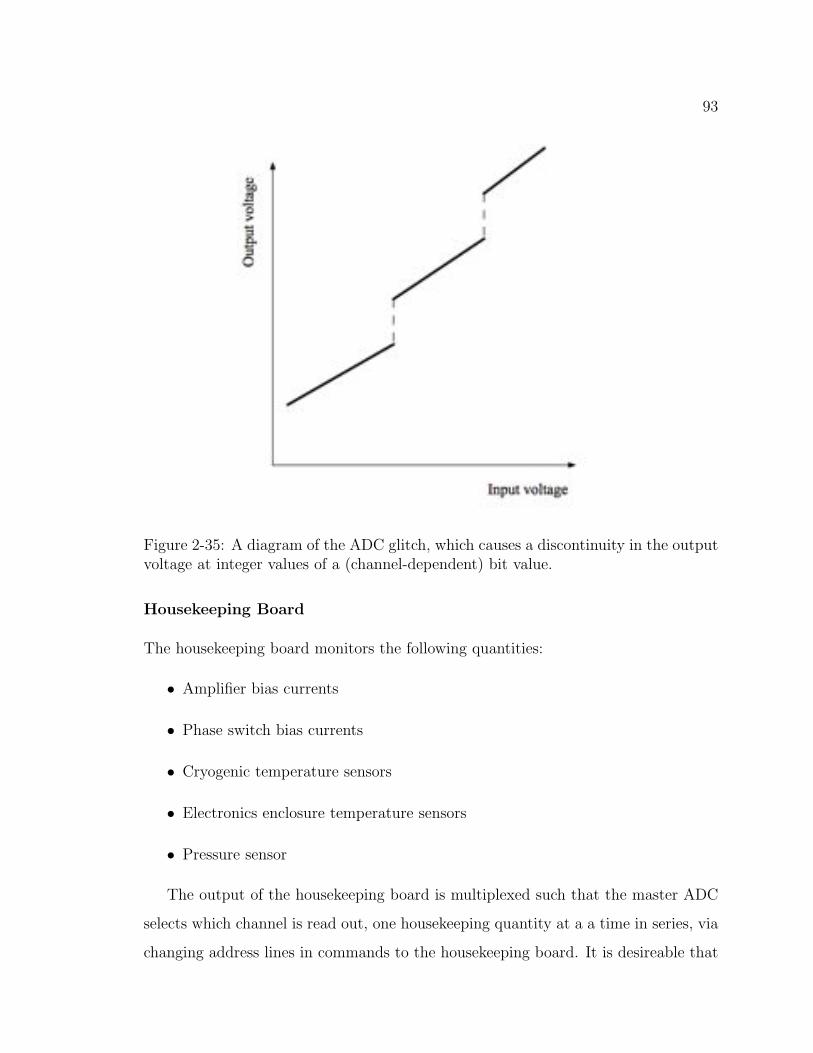
93
Figure 2-35: A diagram of the ADC glitch, which causes a discontinuity in the outputvoltage at integer values of a (channel-dependent) bit value.
Housekeeping Board
The housekeeping board monitors the following quantities:
• Amplifier bias currents
• Phase switch bias currents
• Cryogenic temperature sensors
• Electronics enclosure temperature sensors
• Pressure sensor
The output of the housekeeping board is multiplexed such that the master ADC
selects which channel is read out, one housekeeping quantity at a a time in series, via
changing address lines in commands to the housekeeping board. It is desireable that
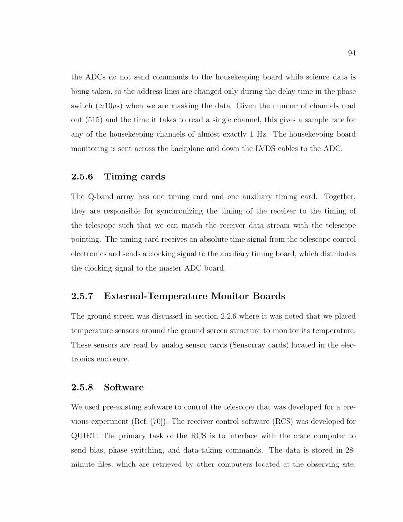
94
the ADCs do not send commands to the housekeeping board while science data is
being taken, so the address lines are changed only during the delay time in the phase
switch (10µs) when we are masking the data. Given the number of channels read
out (515) and the time it takes to read a single channel, this gives a sample rate for
any of the housekeeping channels of almost exactly 1 Hz. The housekeeping board
monitoring is sent across the backplane and down the LVDS cables to the ADC.
2.5.6 Timing cards
The Q-band array has one timing card and one auxiliary timing card. Together,
they are responsible for synchronizing the timing of the receiver to the timing of
the telescope such that we can match the receiver data stream with the telescope
pointing. The timing card receives an absolute time signal from the telescope control
electronics and sends a clocking signal to the auxiliary timing board, which distributes
the clocking signal to the master ADC board.
2.5.7 External-Temperature Monitor Boards
The ground screen was discussed in section 2.2.6 where it was noted that we placed
temperature sensors around the ground screen structure to monitor its temperature.
These sensors are read by analog sensor cards (Sensorray cards) located in the elec-
tronics enclosure.
2.5.8 Software
We used pre-existing software to control the telescope that was developed for a pre-
vious experiment (Ref. [70]). The receiver control software (RCS) was developed for
QUIET. The primary task of the RCS is to interface with the crate computer to
send bias, phase switching, and data-taking commands. The data is stored in 28-
minute files, which are retrieved by other computers located at the observing site.
95
The RCS also contains data flagging to identify periods when the software or receiver
is not working properly. There are 30 flags, they generally look for timing problems
(time-frames dropped, abnormal time separation between stamps, offsets between the
timing between various boards, etc), uneven numbers of data samples for the various
data streams, and phase-switch transition masking problems. A few of the flags are
status flags instead of warning flags, they indicate the phase switch state and the
data-taking rate (we take down-sampled when the telescope is stowed, for example).
96
2.6 Cryostat
2.6.1 Introduction
This section describes the design and performance of the cryostats for the W-band
and Q-band receivers. The primary purpose of each cryostat is to maintain the
modules, feedhorns, and OMTs at a constant cryogenic temperature of 20K over
the observing season.
Both cryostats were designed and tested at Columbia. The design phase included
simulating the mechanical stresses on the system to ensure adequate vacuum and
support for the optics under observing conditions, and computing the expected tem-
peratures for relevant components given anticipated radiative and electrical heating
loads. We validated the cryostats for use by cooling them with heat loading config-
urations meant to mimic the conditions with the receiver array installed. We also
designed and built the cryostat vacuum windows for each of the two receiver ar-
rays. This process included selecting viable materials for both the window and the
anti-reflection (AR) coating, and developing a process for applying the AR coating.
2.6.2 Description of W- and Q- band Cryostats
The cryostat design, including cooling, external components, and internal components
is described in this section.
Cryogenic Cooling
Cryogenic temperatures in each cryostat are achieved with two Gifford-McMahon
dual-stage refrigerators. Each refrigerator is a CTI 1020 with its own 8600 water-
cooled compressor. The first stage of the refrigerator has a minimum temperature of
35K and the second stage of the refrigerator has a minimum temperature of 8K
under zero-load conditions (Ref. [21]).
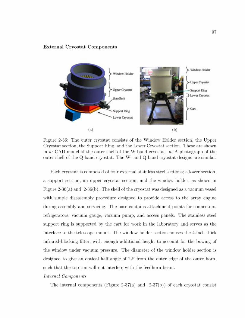
97
External Cryostat Components
(a) (b)
Figure 2-36: The outer cryostat consists of the Window Holder section, the UpperCryostat section, the Support Ring, and the Lower Cryostat section. These are shownin a: CAD model of the outer shell of the W-band cryostat. b: A photograph of theouter shell of the Q-band cryostat. The W- and Q-band cryostat designs are similar.
Each cryostat is composed of four external stainless steel sections; a lower section,
a support section, an upper cryostat section, and the window holder, as shown in
Figure 2-36(a) and 2-36(b). The shell of the cryostat was designed as a vacuum vessel
with simple disassembly procedure designed to provide access to the array engine
during assembly and servicing. The base contains attachment points for connectors,
refrigerators, vacuum gauge, vacuum pump, and access panels. The stainless steel
support ring is supported by the cart for work in the laboratory and serves as the
interface to the telescope mount. The window holder section houses the 4-inch thick
infrared-blocking filter, with enough additional height to account for the bowing of
the window under vacuum pressure. The diameter of the window holder section is
designed to give an optical half angle of 22 from the outer edge of the outer horn,
such that the top rim will not interfere with the feedhorn beam.
Internal Components
The internal components (Figure 2-37(a) and 2-37(b)) of each cryostat consist
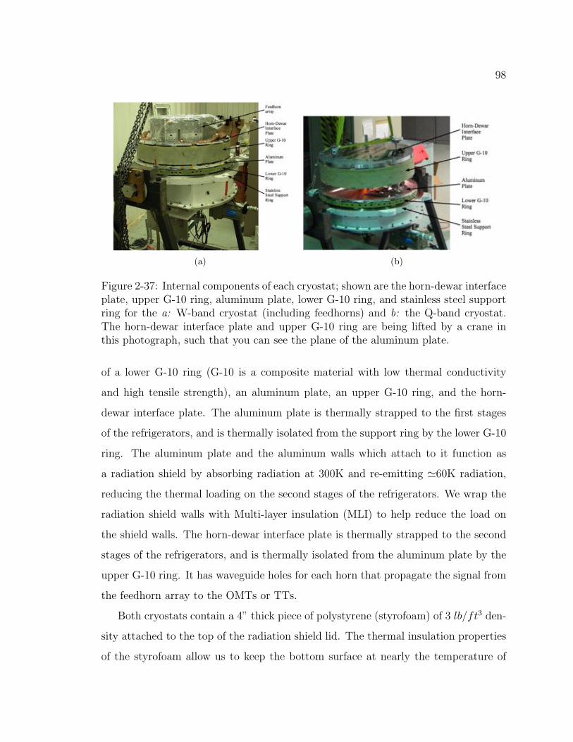
98
(a) (b)
Figure 2-37: Internal components of each cryostat; shown are the horn-dewar interfaceplate, upper G-10 ring, aluminum plate, lower G-10 ring, and stainless steel supportring for the a: W-band cryostat (including feedhorns) and b: the Q-band cryostat.The horn-dewar interface plate and upper G-10 ring are being lifted by a crane inthis photograph, such that you can see the plane of the aluminum plate.
of a lower G-10 ring (G-10 is a composite material with low thermal conductivity
and high tensile strength), an aluminum plate, an upper G-10 ring, and the horn-
dewar interface plate. The aluminum plate is thermally strapped to the first stages
of the refrigerators, and is thermally isolated from the support ring by the lower G-10
ring. The aluminum plate and the aluminum walls which attach to it function as
a radiation shield by absorbing radiation at 300K and re-emitting 60K radiation,
reducing the thermal loading on the second stages of the refrigerators. We wrap the
radiation shield walls with Multi-layer insulation (MLI) to help reduce the load on
the shield walls. The horn-dewar interface plate is thermally strapped to the second
stages of the refrigerators, and is thermally isolated from the aluminum plate by the
upper G-10 ring. It has waveguide holes for each horn that propagate the signal from
the feedhorn array to the OMTs or TTs.
Both cryostats contain a 4” thick piece of polystyrene (styrofoam) of 3 lb/ft3 den-
sity attached to the top of the radiation shield lid. The thermal insulation properties
of the styrofoam allow us to keep the bottom surface at nearly the temperature of
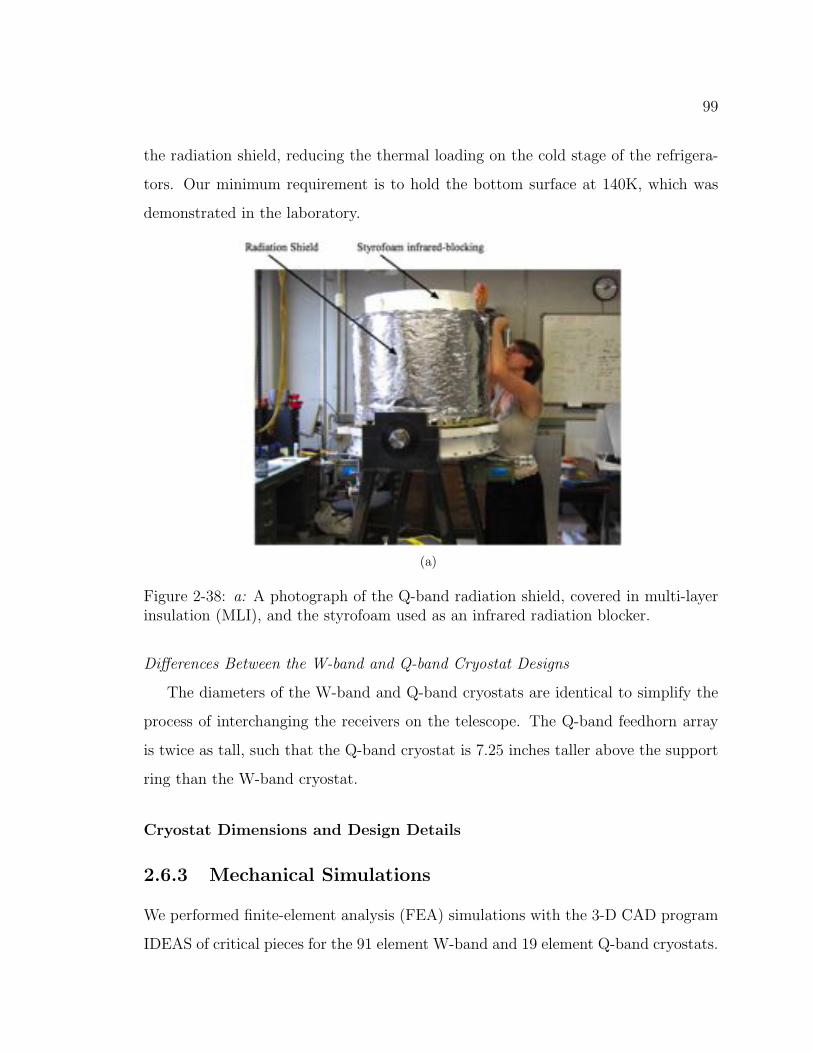
99
the radiation shield, reducing the thermal loading on the cold stage of the refrigera-
tors. Our minimum requirement is to hold the bottom surface at 140K, which was
demonstrated in the laboratory.
(a)
Figure 2-38: a: A photograph of the Q-band radiation shield, covered in multi-layerinsulation (MLI), and the styrofoam used as an infrared radiation blocker.
Differences Between the W-band and Q-band Cryostat Designs
The diameters of the W-band and Q-band cryostats are identical to simplify the
process of interchanging the receivers on the telescope. The Q-band feedhorn array
is twice as tall, such that the Q-band cryostat is 7.25 inches taller above the support
ring than the W-band cryostat.
Cryostat Dimensions and Design Details
2.6.3 Mechanical Simulations
We performed finite-element analysis (FEA) simulations with the 3-D CAD program
IDEAS of critical pieces for the 91 element W-band and 19 element Q-band cryostats.
100
Part W-band Q-band- Height (in) Weight (lbs) Height (in) Weight (lbs)
Lower Cryostat 6.25 127.4 4.25 92.03Stainless Steel Support Ring 1 67 1 67
Upper cryostat 12.125 55.9 19.375 72.8Window Holder 7.25 61 7.25 64.5
Window 0.25” – 0.375 –Totals 26.875 311 31.875 296
Table 2.8: Dimensions of the external elements of each cryostat. Note that the theseweights (both total and separate) do not include masses of the components inside thecryostat, e.g. horns, fridges, OMTs, etc.
The cryostat is mounted on the telescope such that it is oriented sideways with the
length of the cryostat horizonal to the ground. During science observations, the
telescope platform is tilted as much as 70, so it is critically important that we
understand how the design will behave at variety of angles. We focused our studies
on the G-10 rings as they will have the highest stress due to their shape and the
observing orientation. We simulated the effect of rotating the cryostat at a variety
of different orientations, which is accomplished in practice by defining acceleration
vector directions. The definition of the acceleration vectors is shown in Figure 2-39(a).
• X angle refers to a rotation around the axis of the cryostat
• Z angle of zero sets the axis of the cryostat to be horizontal.
Figure 2-39(b) shows the inital orientation from above. Our simulations show
that we are always under ten percent of the maximum stress of G-10 (40,000 psi
lower bound).
2.6.4 Expected and Measured Cryostat Temperatures
Loading on each of the two stages of the refrigerators is presented in this section, with
an estimate of the final temperatures we expected to achieve with each cryostat.
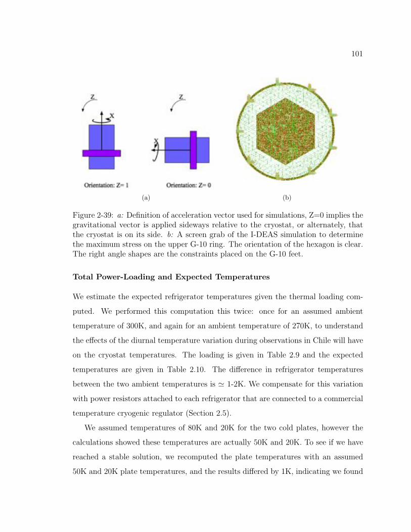
101
(a) (b)
Figure 2-39: a: Definition of acceleration vector used for simulations, Z=0 implies thegravitational vector is applied sideways relative to the cryostat, or alternately, thatthe cryostat is on its side. b: A screen grab of the I-DEAS simulation to determinethe maximum stress on the upper G-10 ring. The orientation of the hexagon is clear.The right angle shapes are the constraints placed on the G-10 feet.
Total Power-Loading and Expected Temperatures
We estimate the expected refrigerator temperatures given the thermal loading com-
puted. We performed this computation this twice: once for an assumed ambient
temperature of 300K, and again for an ambient temperature of 270K, to understand
the effects of the diurnal temperature variation during observations in Chile will have
on the cryostat temperatures. The loading is given in Table 2.9 and the expected
temperatures are given in Table 2.10. The difference in refrigerator temperatures
between the two ambient temperatures is 1-2K. We compensate for this variation
with power resistors attached to each refrigerator that are connected to a commercial
temperature cryogenic regulator (Section 2.5).
We assumed temperatures of 80K and 20K for the two cold plates, however the
calculations showed these temperatures are actually 50K and 20K. To see if we have
reached a stable solution, we recomputed the plate temperatures with an assumed
50K and 20K plate temperatures, and the results differed by 1K, indicating we found
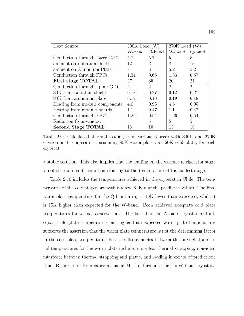
102
Heat Source 300K Load (W) 270K Load (W)W-band Q-band W-band Q-band
Conduction through lower G-10 5.7 5.7 5 5ambient on radiation shield 12 21 8 13ambient on Aluminum Plate 8 8 5.2 5.2Conduction through FPCs 1.54 0.66 1.33 0.57First stage TOTAL: 27 35 20 21Conduction through upper G-10 2 2 2 280K from radiation shield 0.12 0.27 0.12 0.2780K from aluminum plate 0.19 0.18 0.19 0.18Heating from module components 4.6 0.95 4.6 0.95Heating from module boards 1.1 0.47 1.1 0.47Conduction through FPCs 1.26 0.54 1.26 0.54Radiation from window 5 5 5 5Second Stage TOTAL: 13 10 13 10
Table 2.9: Calculated thermal loading from various sources with 300K and 270Kenvironment temperature, assuming 80K warm plate and 20K cold plate, for eachcryostat.
a stable solution. This also implies that the loading on the warmer refrigerator stage
is not the dominant factor contributing to the temperature of the coldest stage.
Table 2.10 includes the temperatures achieved in the cryostat in Chile. The tem-
perature of the cold stages are within a few Kelvin of the predicted values. The final
warm plate temperature for the Q-band array is 10K lower than expected, while it
is 15K higher than expected for the W-band. Both achieved adequate cold plate
temperatures for science observations. The fact that the W-band cryostat had ad-
equate cold plate temperatures but higher than expected warm plate temperatures
supports the assertion that the warm plate temperature is not the determining factor
in the cold plate temperature. Possible discrepancies between the predicted and fi-
nal temperatures for the warm plate include: non-ideal thermal strapping, non-ideal
interfaces between thermal strapping and plates, and loading in excess of predictions
from IR sources or from expectations of MLI performance for the W-band cryostat.
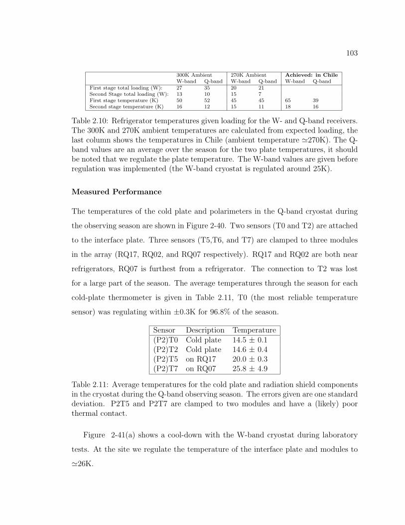
103
300K Ambient 270K Ambient Achieved: in ChileW-band Q-band W-band Q-band W-band Q-band
First stage total loading (W): 27 35 20 21
Second Stage total loading (W): 13 10 15 7
First stage temperature (K) 50 52 45 45 65 39
Second stage temperature (K) 16 12 15 11 18 16
Table 2.10: Refrigerator temperatures given loading for the W- and Q-band receivers.The 300K and 270K ambient temperatures are calculated from expected loading, thelast column shows the temperatures in Chile (ambient temperature 270K). The Q-band values are an average over the season for the two plate temperatures, it shouldbe noted that we regulate the plate temperature. The W-band values are given beforeregulation was implemented (the W-band cryostat is regulated around 25K).
Measured Performance
The temperatures of the cold plate and polarimeters in the Q-band cryostat during
the observing season are shown in Figure 2-40. Two sensors (T0 and T2) are attached
to the interface plate. Three sensors (T5,T6, and T7) are clamped to three modules
in the array (RQ17, RQ02, and RQ07 respectively). RQ17 and RQ02 are both near
refrigerators, RQ07 is furthest from a refrigerator. The connection to T2 was lost
for a large part of the season. The average temperatures through the season for each
cold-plate thermometer is given in Table 2.11, T0 (the most reliable temperature
sensor) was regulating within ±0.3K for 96.8% of the season.
Sensor Description Temperature(P2)T0 Cold plate 14.5 ± 0.1(P2)T2 Cold plate 14.6 ± 0.4(P2)T5 on RQ17 20.0 ± 0.3(P2)T7 on RQ07 25.8 ± 4.9
Table 2.11: Average temperatures for the cold plate and radiation shield componentsin the cryostat during the Q-band observing season. The errors given are one standarddeviation. P2T5 and P2T7 are clamped to two modules and have a (likely) poorthermal contact.
Figure 2-41(a) shows a cool-down with the W-band cryostat during laboratory
tests. At the site we regulate the temperature of the interface plate and modules to
26K.
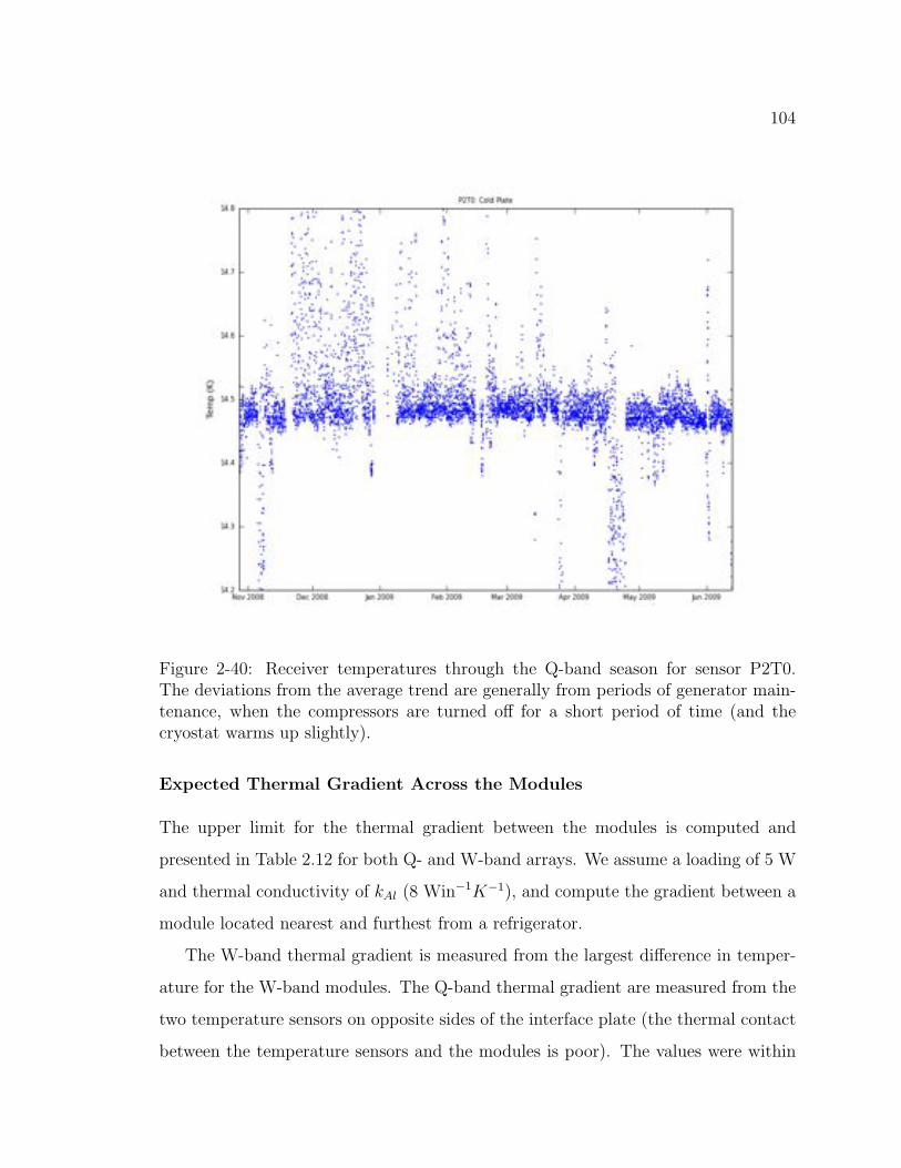
104
Figure 2-40: Receiver temperatures through the Q-band season for sensor P2T0.The deviations from the average trend are generally from periods of generator main-tenance, when the compressors are turned off for a short period of time (and thecryostat warms up slightly).
Expected Thermal Gradient Across the Modules
The upper limit for the thermal gradient between the modules is computed and
presented in Table 2.12 for both Q- and W-band arrays. We assume a loading of 5 W
and thermal conductivity of kAl (8 Win−1K−1), and compute the gradient between a
module located nearest and furthest from a refrigerator.
The W-band thermal gradient is measured from the largest difference in temper-
ature for the W-band modules. The Q-band thermal gradient are measured from the
two temperature sensors on opposite sides of the interface plate (the thermal contact
between the temperature sensors and the modules is poor). The values were within
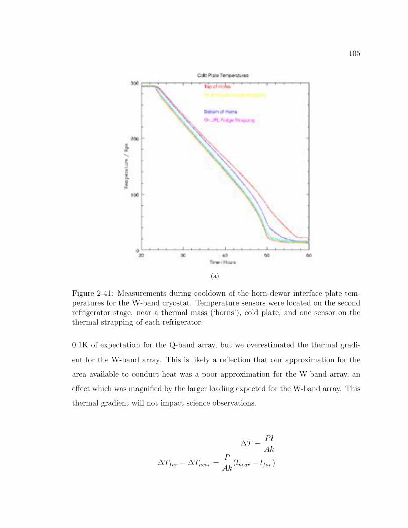
105
(a)
Figure 2-41: Measurements during cooldown of the horn-dewar interface plate tem-peratures for the W-band cryostat. Temperature sensors were located on the secondrefrigerator stage, near a thermal mass (‘horns’), cold plate, and one sensor on thethermal strapping of each refrigerator.
0.1K of expectation for the Q-band array, but we overestimated the thermal gradi-
ent for the W-band array. This is likely a reflection that our approximation for the
area available to conduct heat was a poor approximation for the W-band array, an
effect which was magnified by the larger loading expected for the W-band array. This
thermal gradient will not impact science observations.
∆T =Pl
Ak
∆Tfar −∆Tnear =P
Ak(lnear − lfar)
106
W-band Q-bandPlate thickness (inches) 0.25 0.768Expected Gradient (K) 4 1.5Measured gradient (K) 2.7 1.4
Table 2.12: Calculated thermal gradient from a module closest to the refrigeratorto the module furthest from the refrigerator attachment. The measured values formodules at the site is presented in the last row.
2.6.5 The Cryostat Window
The vacuum window of the cryostat must be strong enough to withstand vacuum
pressure, and also should maximize transmission of the signal to have the smallest
possible degradation of instrument signal-to-noise. This section describes the methods
we used to select the window materials, and our estimate of the contribution to the
system noise from the window.
Window Material
The cryostat windows are 22 inches in diameter, the largest vacuum window of its
kind to date. The material used for the window must be strong enough to withstand
the 5500 lbs of force exterted on the window when the cryostat is at vacuum. We
used a small vacuum chamber to test a variety of materials, Table 2.13 lists the first
materials we tried, their thicknesses, and the results of each test.
Vacuum Window
The loss tangent (tan(δ)) is a measurement of absorption in the material; smaller
values are preferable because the relationship between absorption and the loss tangent
is exponential. Polyethylene-based windows had the best transmission properties, but
the high-density polyethylene (HDPE) windows broke along the edges of the window
after 1-2 vacuum pump-downs in the QUIET cryostats, so we chose to use ultra-
high molecular-weight polyethylene (UHMW-PE) instead. We vacuum pumped the
windows multiple times, measuring the bowing each time. After 20 repetitions it was
107
Material Thickness, mil (mm) Test Results tan δ n
Mylar (PETP) 2 (0.0508) failed 44 ×10−4 1.73Polypropylene 54 (1.37) failed 7.3×10⁻⁴ 1.5
158 (4) bowed in 3”256 (6.5) bowed in 2”
HDPE 35 (0.9) failed 2.5×10⁻⁴ 1.5280 (2) bowed in 3”250 (6.4) bowed in 1.14”
UHMW-PE 78.74 (2) bowed in 3” 2.5×10−4* 1.52 *
Table 2.13: Window Testing Results. HDPE = high-density polyethylene, UHMW-PE=ultra-high molecular-weight polyethylene.* Assumed, no literature on microwave properties of UHMW-PE
determined the window was sufficiently strong.
We could not find an index of refraction and loss tangent for UHMW in the
literature. However, the variation of the index of refraction for the polytheylenes is
small (2%), and it was decided we could approximate the microwave properties of
UHMW-PE from the other polyethylenes. The transmission properties of UHMW-PE
were confirmed in subsequent measurements of the windows (Section 2.6.5).
The index of refraction and loss tangent of HDPE over a range of frequencies is
shown in Figure 2-42. The index of refraction varies only slightly over the measured
frequency range, so for the purposes of studying window transmission and its impact
on system noise we chose to approximate the index of refraction as a constant over
the QUIET frequency bands. We use a value for the index of refraction of HDPE
to be nHDPE=1.525 and the loss tangent for HDPE of tan(δ)=2.5×10⁻⁴ (the value
of the fit line at 90 GHz) to estimate the loss in the QUIET bands. Overestimating
the loss tangent will yield an overestimate of the noise contribution from the window,
and so the values derived will be conservative estimates of the noise contribution to
the system.
Anti-reflection Coating Material
108
Figure 2-42: Index of refraction and loss tangent over a range of frequencies (valuesfrom Ref. [54]). The QUIET frequency band is shown as 35-115 GHz. A horizontalline is drawn at the index of refraction we chose for HDPE, and the two fit lines forthe loss tangent of HDPE and teflon are shown. We used values at 90 GHz for theloss tangent: 3×10⁻⁴ for HDPE and 2.5×10⁻⁴ for teflon.
The condition for zero reflection in a single-layer film (Ref. [35]) is:
n2
ARcoating = nairnUHMWPE (2.43)
With nair = 1 and nUHMWPE= 1.525, our AR coating material should have
n=1.2. The index of refraction of Zitex or Mupor expanded teflon was measured
to be n = 1.2 ± 0.07 (Ref. [5]) in the frequency range 400-1350 GHz, a well-matched
anti-reflection material for the UHMW-PE vacuum window.
Ref. [5] included a comparison with non-expanded teflon, with index of refraction
n=1.44, and noted that the expected index of refraction of teflon with a 50% filling
109
factor (the decrease in density between teflon and expanded teflon) is predicted to
yield an index of refraction of 1.22, confirming their measurement within error. We
will approximate the index of refraction of expanded as constant, using the trend for
non-expanded teflon as a guide, and use the loss tangent of non-expanded teflon at 90
GHz as the loss tangent of expanded teflon (which will overestimate the absorption
and hence the noise temperature contribution). For the following analysis, we will
estimate the loss tangent of the teflon layers as tan(δ) = 3×10⁻⁴.
AR Coating Adhesion
We adhere the teflon to the UHMW-PE window by placing an intermediate layer
of LDPE between the teflon and the UHMW-PE. We then heat the materials above
the melting point of LDPE while applying clamping pressure. This method was
developed at Columbia as part of a technology development effort for multi-layer
metal-mesh filters. LDPE is ideal for this purpose because its melting point is lower
than either teflon or UHMW-PE, and should have similar optical properties as the
latter. We demonstrated our ability to fuse teflon to UHMW-PE with a small test
piece, and then scaled the press to the larger size required for the W- and Q-band
windows. We avoid trapping air bubbles between the material layers by performing
this hot-pressing in a vacuum chamber.
Window Transmission
We present the transmission formalism that will be used to calculate the transmission
curves for our windows. The formulas are valid only for normal incidence, the effects
from the curvature of the window are discussed in Section 2.6.5..
General Transmission and Absorption Matrix Formalism
Transmission through a material and through an interface is given by (Ref. [43]):
Tlayer
=
eikiti 0
0 e−ikiti
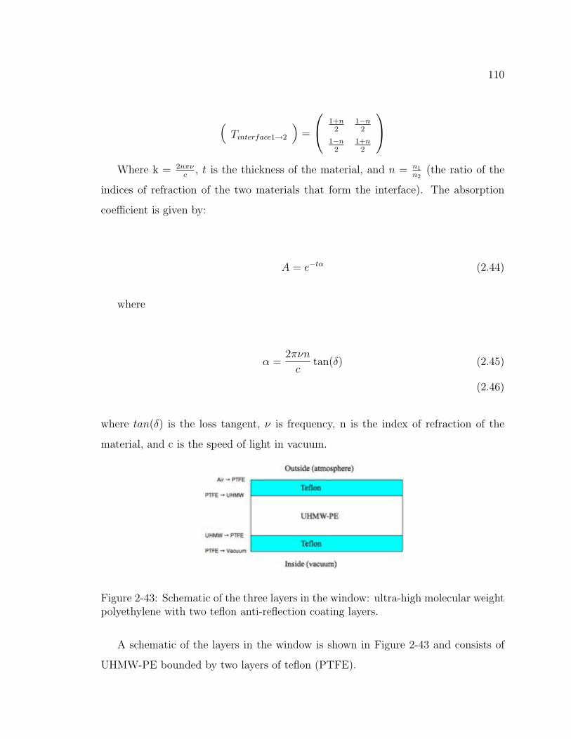
110
Tinterface1→2
=
1+n
2
1−n2
1−n2
1+n2
Where k = 2nπνc , t is the thickness of the material, and n = n1
n2(the ratio of the
indices of refraction of the two materials that form the interface). The absorption
coefficient is given by:
A = e−tα (2.44)
where
α =2πνn
ctan(δ) (2.45)
(2.46)
where tan(δ) is the loss tangent, ν is frequency, n is the index of refraction of the
material, and c is the speed of light in vacuum.
Figure 2-43: Schematic of the three layers in the window: ultra-high molecular weightpolyethylene with two teflon anti-reflection coating layers.
A schematic of the layers in the window is shown in Figure 2-43 and consists of
UHMW-PE bounded by two layers of teflon (PTFE).
111
Eout =TtransferEincident (2.47)
Ttransfer =TPTFE→air[TPTFEAPTFE]
× TUHMW→PTFE[TUHMW AUHMW ]TPTFE→UHMW
× [TPTFEAPTFE]Tair→PTFE
The exponential in the propagation term changes sign in the transmission matrix
depending on the direction of wave travel. The absorption does not have this direc-
tional dependence and is proportional to the identity matrix, so the sign is always
the same and can be re-arranged in the transfer matrix as a constant factor. The
transmitted and reflected components of the transmission matrix are expressed as
(Ref. [43]):
Etrans =Det[Ttransfer]
T22
Eincident
Erefl =−T21
T22
Eincident
Where Einc is the incident signal and T22 is the (2,2) element of the 2×2 Ttransfer
matrix. This yields the transmission coefficient (T = |Etrans|2) and reflection coeffi-
cient (R = |Erefl|2).
Measured and Expected Window Transmission Properties
After stress-testing a variety of UHMW-PE samples, we computed the expected
transmission and reflection properties of the W- and Q-band windows for the “off-the-
shelf” plastics which had material thicknesses nearest to integer wavelengths of the
material. We produced samples of anti-reflection coated W-band window and mea-
sured its transmission properties in a vector-network-analyzer (VNA). A schematic
of the VNA testing apparatus is depicted in Figure 2-44: it consists of two standard
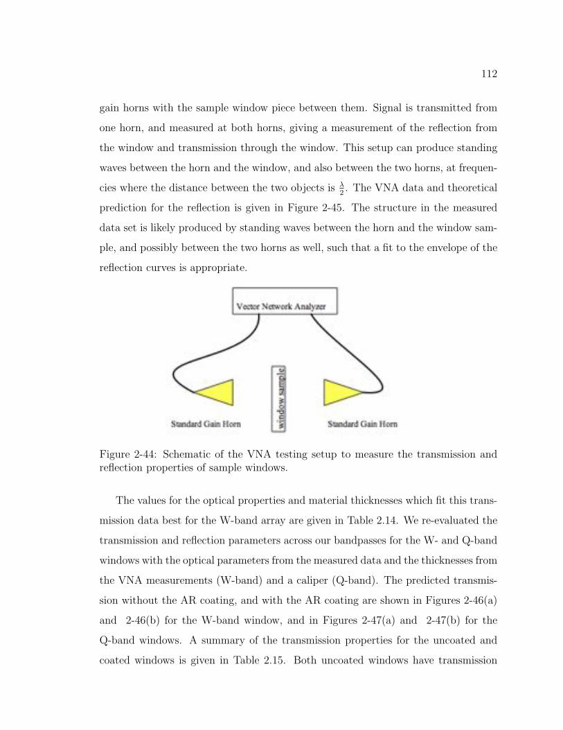
112
gain horns with the sample window piece between them. Signal is transmitted from
one horn, and measured at both horns, giving a measurement of the reflection from
the window and transmission through the window. This setup can produce standing
waves between the horn and the window, and also between the two horns, at frequen-
cies where the distance between the two objects is λ2. The VNA data and theoretical
prediction for the reflection is given in Figure 2-45. The structure in the measured
data set is likely produced by standing waves between the horn and the window sam-
ple, and possibly between the two horns as well, such that a fit to the envelope of the
reflection curves is appropriate.
Figure 2-44: Schematic of the VNA testing setup to measure the transmission andreflection properties of sample windows.
The values for the optical properties and material thicknesses which fit this trans-
mission data best for the W-band array are given in Table 2.14. We re-evaluated the
transmission and reflection parameters across our bandpasses for the W- and Q-band
windows with the optical parameters from the measured data and the thicknesses from
the VNA measurements (W-band) and a caliper (Q-band). The predicted transmis-
sion without the AR coating, and with the AR coating are shown in Figures 2-46(a)
and 2-46(b) for the W-band window, and in Figures 2-47(a) and 2-47(b) for the
Q-band windows. A summary of the transmission properties for the uncoated and
coated windows is given in Table 2.15. Both uncoated windows have transmission
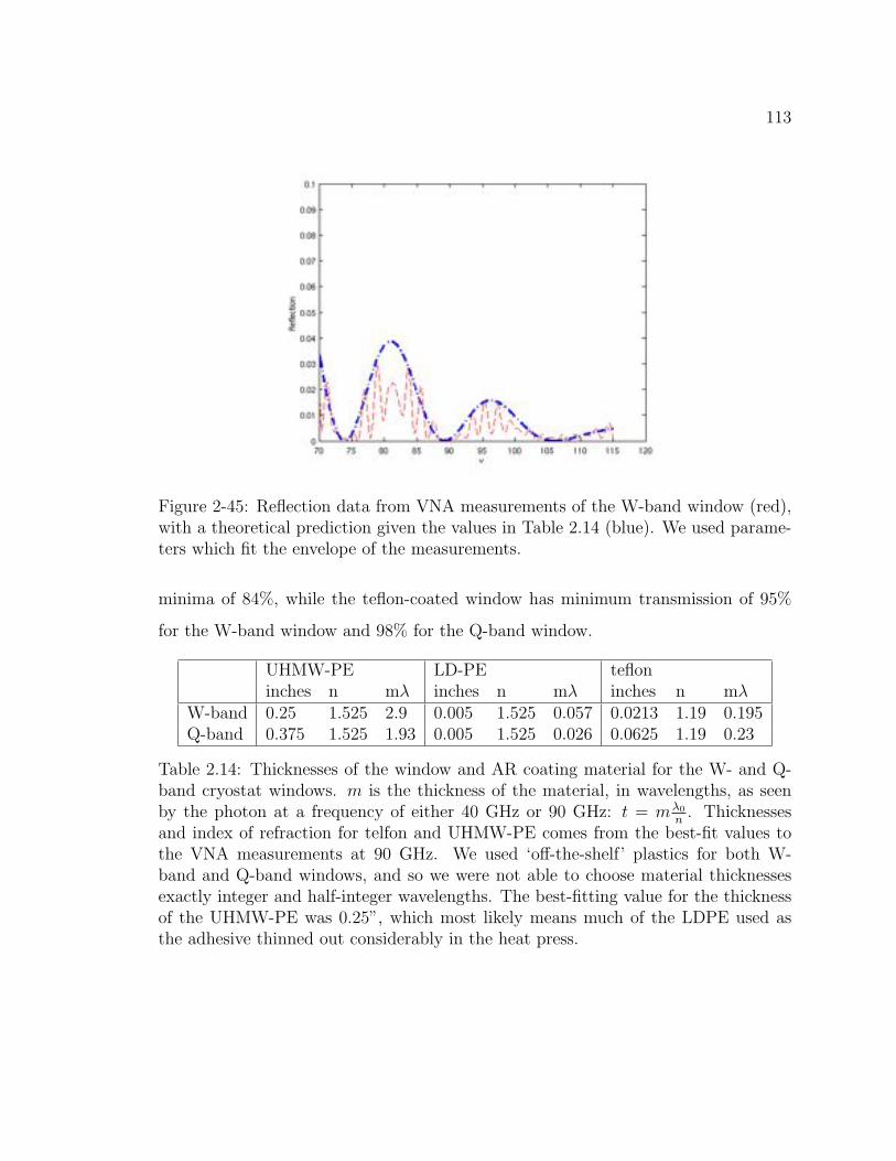
113
Figure 2-45: Reflection data from VNA measurements of the W-band window (red),with a theoretical prediction given the values in Table 2.14 (blue). We used parame-ters which fit the envelope of the measurements.
minima of 84%, while the teflon-coated window has minimum transmission of 95%
for the W-band window and 98% for the Q-band window.
UHMW-PE LD-PE tefloninches n mλ inches n mλ inches n mλ
W-band 0.25 1.525 2.9 0.005 1.525 0.057 0.0213 1.19 0.195Q-band 0.375 1.525 1.93 0.005 1.525 0.026 0.0625 1.19 0.23
Table 2.14: Thicknesses of the window and AR coating material for the W- and Q-band cryostat windows. m is the thickness of the material, in wavelengths, as seenby the photon at a frequency of either 40 GHz or 90 GHz: t = m
λ0n . Thicknesses
and index of refraction for telfon and UHMW-PE comes from the best-fit values tothe VNA measurements at 90 GHz. We used ‘off-the-shelf’ plastics for both W-band and Q-band windows, and so we were not able to choose material thicknessesexactly integer and half-integer wavelengths. The best-fitting value for the thicknessof the UHMW-PE was 0.25”, which most likely means much of the LDPE used asthe adhesive thinned out considerably in the heat press.
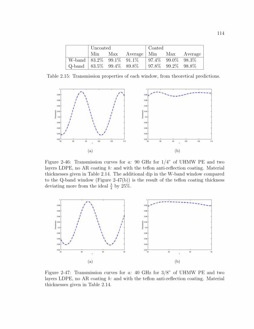
114
Uncoated CoatedMin Max Average Min Max Average
W-band 83.2% 99.1% 91.1% 97.4% 99.0% 98.3%Q-band 83.5% 99.4% 89.8% 97.8% 99.2% 98.8%
Table 2.15: Transmission properties of each window, from theoretical predictions.
(a) (b)
Figure 2-46: Transmission curves for a: 90 GHz for 1/4” of UHMW PE and twolayers LDPE, no AR coating b: and with the teflon anti-reflection coating. Materialthicknesses given in Table 2.14. The additional dip in the W-band window comparedto the Q-band window (Figure 2-47(b)) is the result of the teflon coating thicknessdeviating more from the ideal λ
4by 25%.
(a) (b)
Figure 2-47: Transmission curves for a: 40 GHz for 3/8” of UHMW PE and twolayers LDPE, no AR coating b: and with the teflon anti-reflection coating. Materialthicknesses given in Table 2.14.
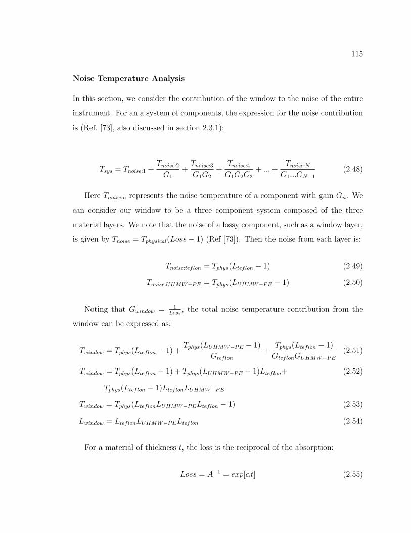
115
Noise Temperature Analysis
In this section, we consider the contribution of the window to the noise of the entire
instrument. For an a system of components, the expression for the noise contribution
is (Ref. [73], also discussed in section 2.3.1):
Tsys = Tnoise:1 +Tnoise:2
G1
+Tnoise:3
G1G2
+Tnoise:4
G1G2G3
+ ... +Tnoise:N
G1...GN−1
(2.48)
Here Tnoise:n represents the noise temperature of a component with gain Gn. We
can consider our window to be a three component system composed of the three
material layers. We note that the noise of a lossy component, such as a window layer,
is given by Tnoise = Tphysical(Loss− 1) (Ref [73]). Then the noise from each layer is:
Tnoise:teflon = Tphys(Lteflon − 1) (2.49)
Tnoise:UHMW−PE = Tphys(LUHMW−PE − 1) (2.50)
Noting that Gwindow = 1
Loss , the total noise temperature contribution from the
window can be expressed as:
Twindow = Tphys(Lteflon − 1) +Tphys(LUHMW−PE − 1)
Gteflon+
Tphys(Lteflon − 1)
GteflonGUHMW−PE(2.51)
Twindow = Tphys(Lteflon − 1) + Tphys(LUHMW−PE − 1)Lteflon+ (2.52)
Tphys(Lteflon − 1)LteflonLUHMW−PE
Twindow = Tphys(LteflonLUHMW−PELteflon − 1) (2.53)
Lwindow = LteflonLUHMW−PELteflon (2.54)
For a material of thickness t, the loss is the reciprocal of the absorption:
Loss = A−1 = exp[αt] (2.55)
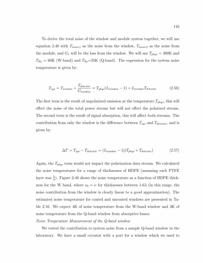
116
To derive the total noise of the window and module system together, we will use
equation 2.48 with Tnoise:1 as the noise from the window, Tnoise:2 as the noise from
the module, and G1 will be the loss from the window. We will use Tphys = 300K and
TRx = 60K (W-band) and TRx=35K (Q-band). The expression for the system noise
temperature is given by:
Tsys = Twindow +Tdetector
Gwindow= Tphys(Lwindow − 1) + LwindowTdetector (2.56)
The first term is the result of unpolarized emission at the temperature Tphys, this will
effect the noise of the total power stream but will not effect the polarized stream.
The second term is the result of signal absorption, this will affect both streams. The
contribution from only the window is the difference between Tsys and Tdetector, and is
given by:
∆T = Tsys − Tdetector = (Lwindow − 1)(Tphys + Tdetector) (2.57)
Again, the Tphys term would not impact the polarization data stream. We calculated
the noise temperatures for a range of thicknesses of HDPE (assuming each PTFE
layer was λ4). Figure 2-48 shows the noise temperature as a function of HDPE thick-
ness for the W band, where ν0 = ν for thicknesses between 1-6λ (in this range, the
noise contribution from the window is clearly linear to a good approximation). The
estimated noise temperature for coated and uncoated windows are presented in Ta-
ble 2.16. We expect 4K of noise temperature from the W-band window and 3K of
noise temperature from the Q-band window from absorptive losses.
Noise Temperature Measurement of the Q-band window
We tested the contribution to system noise from a sample Q-band window in the
laboratory. We have a small cryostat with a port for a window which we used to
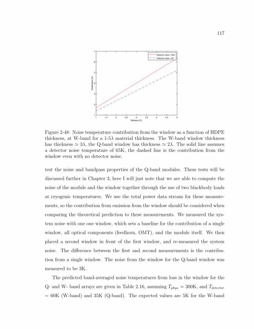
117
Figure 2-48: Noise temperature contribution from the window as a function of HDPEthickness, at W-band for a 1-5λ material thickness. The W-band window thicknesshas thickness 3λ, the Q-band window has thickness 2λ. The solid line assumesa detector noise temperature of 65K, the dashed line is the contribution from thewindow even with no detector noise.
test the noise and bandpass properties of the Q-band modules. These tests will be
discussed further in Chapter 3, here I will just note that we are able to compute the
noise of the module and the window together through the use of two blackbody loads
at cryogenic temperatures. We use the total power data stream for these measure-
ments, so the contribution from emission from the window should be considered when
comparing the theoretical prediction to these measurements. We measured the sys-
tem noise with one one window, which sets a baseline for the contribution of a single
window, all optical components (feedhorn, OMT), and the module itself. We then
placed a second window in front of the first window, and re-measured the system
noise. The difference between the first and second measurements is the contribu-
tion from a single window. The noise from the window for the Q-band window was
measured to be 3K.
The predicted band-averaged noise temperatures from loss in the window for the
Q- and W- band arrays are given in Table 2.16, assuming Tphys = 300K, and Tdetector
= 60K (W-band) and 35K (Q-band). The expected values are 5K for the W-band
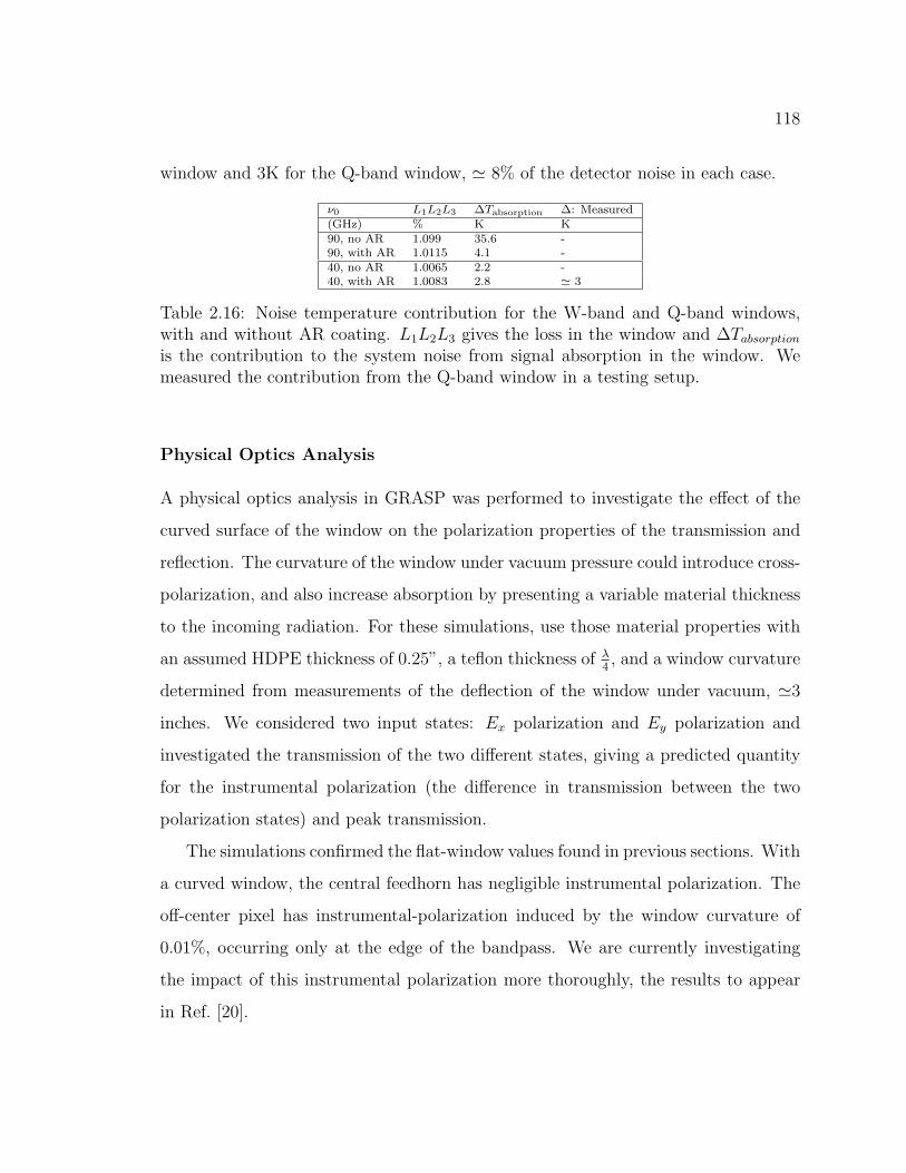
118
window and 3K for the Q-band window, 8% of the detector noise in each case.
ν0 L1L2L3 ∆Tabsorption ∆: Measured
(GHz) % K K
90, no AR 1.099 35.6 -
90, with AR 1.0115 4.1 -
40, no AR 1.0065 2.2 -
40, with AR 1.0083 2.8 3
Table 2.16: Noise temperature contribution for the W-band and Q-band windows,with and without AR coating. L1L2L3 gives the loss in the window and ∆Tabsorption
is the contribution to the system noise from signal absorption in the window. Wemeasured the contribution from the Q-band window in a testing setup.
Physical Optics Analysis
A physical optics analysis in GRASP was performed to investigate the effect of the
curved surface of the window on the polarization properties of the transmission and
reflection. The curvature of the window under vacuum pressure could introduce cross-
polarization, and also increase absorption by presenting a variable material thickness
to the incoming radiation. For these simulations, use those material properties with
an assumed HDPE thickness of 0.25”, a teflon thickness of λ4, and a window curvature
determined from measurements of the deflection of the window under vacuum, 3
inches. We considered two input states: Ex polarization and Ey polarization and
investigated the transmission of the two different states, giving a predicted quantity
for the instrumental polarization (the difference in transmission between the two
polarization states) and peak transmission.
The simulations confirmed the flat-window values found in previous sections. With
a curved window, the central feedhorn has negligible instrumental polarization. The
off-center pixel has instrumental-polarization induced by the window curvature of
0.01%, occurring only at the edge of the bandpass. We are currently investigating
the impact of this instrumental polarization more thoroughly, the results to appear
in Ref. [20].
Chapter 3
Q-band Array Integration,
Characterization, and Testing
3.1 Introduction
We integrated the feedhorns, OMTs, modules, and electronics boards together to form
the Q-band QUIET receiver. We measured the bandpasses, noise, and responsivity
of the receiver in the laboratory to verify that everything was properly characterized
before beginning science observations. This chapter addresses Q-band instrument
characterization and testing prior to observations in Chile.
3.2 Bandpasses
Bandpasses were measured for each diode of each module both in the laboratory
during the course of array testing, and also during final calibration at the site in June
2009. We used a signal generator with standard gain horn to inject a polarized signal
at frequencies in the range 35-50GHz into the receiver and measure response as a
function of frequency (each sweep through the passband frequency range is termed a
‘bandsweep’). These measurements can be used to calculate bandwidths and central
119
120
frequencies.
The equation for the effective central frequency (Ref. [71]) is:
Central Frequency: νe =
νI(ν)Ae(ν)σ(ν)dνf(ν)Ae(ν)σ(ν)dν
(3.1)
(no equivalent was given in the Reference for the bandwidth, however the extension
to bandwidth is straightforward) where I(ν) is the response of the receiver and the
optics, Ae(ν) is the effective area of the source in the beam at each frequency (it is
not immediately obvious that this should be true, it was however found to be true in
calibration measurements, described in Section 5.9), and σ(ν) is the spectrum of the
source in thermodynamic temperature units. With these approximations, and noting
that the source spectrum σ(ν) is convolved with the module bandpass I(ν) to obtain
the bandpass we measure, yields:
Central Frequency:
IσνdνIσdν
const.∆ν−→
IσνIσ
(3.2)
Bandwidth:
Iσdν
2
(Iσ)2dν
const.∆ν−→
[
Iσ]2∆ν(Iσ)2
(3.3)
We flatten the output of the signal generator so that the measured bandpass has no
contribution from the signal generator bandpass. Thus we can set σ = 1 to compute
the central frequency and bandwidth:
Central Frequency:
IνI
(3.4)
Bandwidth:[
I]2∆νI2
(3.5)
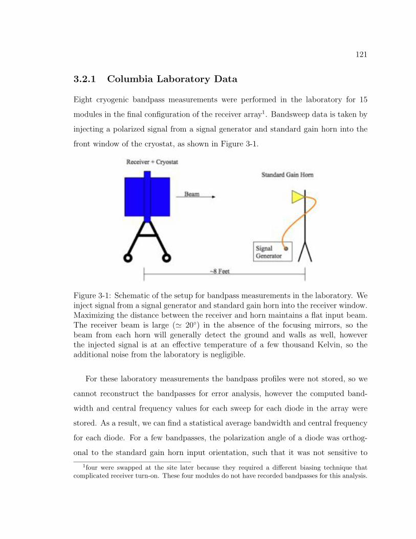
121
3.2.1 Columbia Laboratory Data
Eight cryogenic bandpass measurements were performed in the laboratory for 15
modules in the final configuration of the receiver array1. Bandsweep data is taken by
injecting a polarized signal from a signal generator and standard gain horn into the
front window of the cryostat, as shown in Figure 3-1.
Figure 3-1: Schematic of the setup for bandpass measurements in the laboratory. Weinject signal from a signal generator and standard gain horn into the receiver window.Maximizing the distance between the receiver and horn maintains a flat input beam.The receiver beam is large ( 20) in the absence of the focusing mirrors, so thebeam from each horn will generally detect the ground and walls as well, howeverthe injected signal is at an effective temperature of a few thousand Kelvin, so theadditional noise from the laboratory is negligible.
For these laboratory measurements the bandpass profiles were not stored, so we
cannot reconstruct the bandpasses for error analysis, however the computed band-
width and central frequency values for each sweep for each diode in the array were
stored. As a result, we can find a statistical average bandwidth and central frequency
for each diode. For a few bandpasses, the polarization angle of a diode was orthog-
onal to the standard gain horn input orientation, such that it was not sensitive to
1four were swapped at the site later because they required a different biasing technique thatcomplicated receiver turn-on. These four modules do not have recorded bandpasses for this analysis.
122
the signal1. These bandpass measurements have unrealistically low or high computed
bandwidths, so any scan with a bandwidth less that 6 GHz or greater than 9 GHz was
removed from the data set. For a given diode, the remaining bandwidths and central
frequencies were averaged and the standard deviation was computed. The central
frequencies and bandwidths for the polarization modules are given in Tables 3.1 and
3.2.
3.2.2 Site Data
Bandpasses were measured with the Q-band receiver at the site in Chile over the
course of two days (June 13 and 14, 2009) in four different data sets, yielding a total
of 35 bandsweeps. A schematic of the experimental setup is shown in Figure 3-2.
The carrier wave signal is produced by the signal generator, transmitted by radio-
frequency cabling to a standard gain horn, where it is broadcast to a 6 × 6 square
reflector plate, and reflected into the primary mirror. We positioned the reflector plate
over the center of the primary, with the horn roughly 4 feet away. Alignment was
performed by tuning the signal generator to output a carrier wave at 42.5 GHz and
rotating the horn until it maximized the signal on the Q diodes for the largest number
of modules possible. This would allow us to perform a second set of measurements
for the U diodes, and ensure we had high quality bandpasses for most diodes. A
spike was inserted at 37 GHz to reference the detector measurements in frequency.
The data were taken in ‘double demodulation’ mode (see section 2.3). The measured
signal is a combination of the signal generator carrier wave signal and any additional
reflections in the system (e.g. off of any exposed metal in the ground shield, between
the mirrors and the reflector plate, and between the horn and the reflector plate).
Unfortunately the signal generator stopped sweeping after the first three sweeps
on the second day of data-taking, so measurements we performed to maximize the
1We did not phase-switch the phase switches for these measurements and without phase switchingthere could be a horn orientation that happens to be orthogonal to (for example) the +Q axis ofthe module, resulting in a bandpass which is only noise.
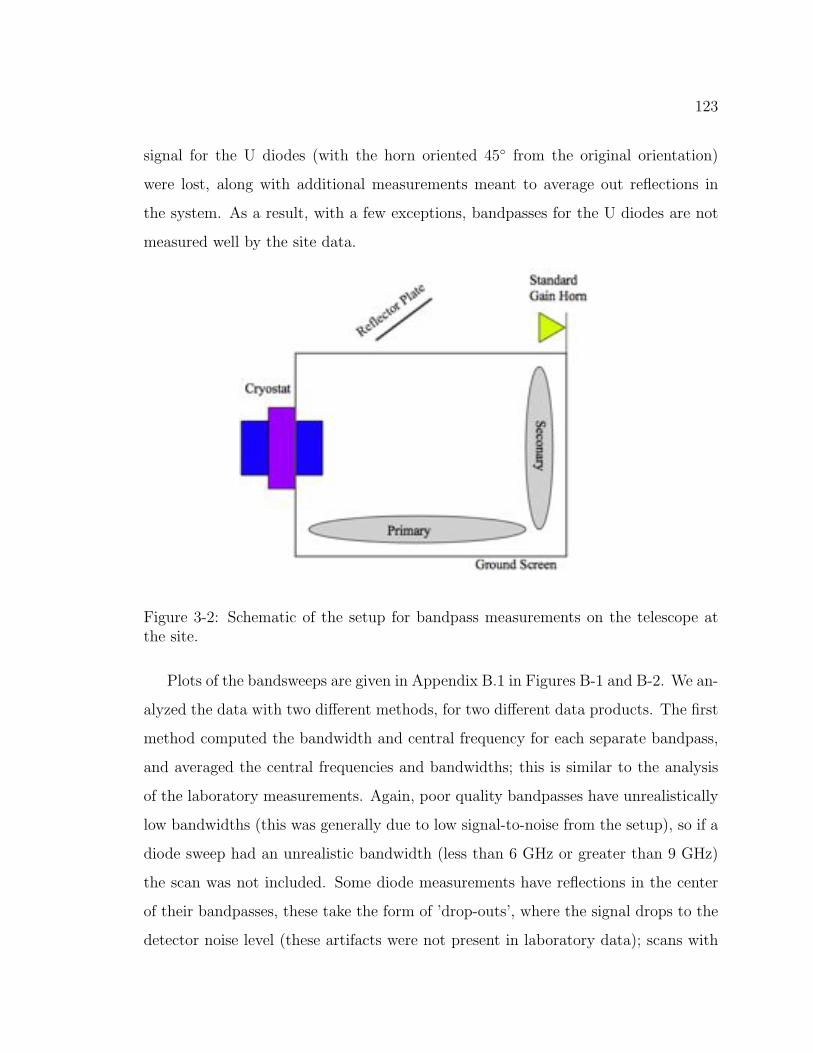
123
signal for the U diodes (with the horn oriented 45 from the original orientation)
were lost, along with additional measurements meant to average out reflections in
the system. As a result, with a few exceptions, bandpasses for the U diodes are not
measured well by the site data.
Figure 3-2: Schematic of the setup for bandpass measurements on the telescope atthe site.
Plots of the bandsweeps are given in Appendix B.1 in Figures B-1 and B-2. We an-
alyzed the data with two different methods, for two different data products. The first
method computed the bandwidth and central frequency for each separate bandpass,
and averaged the central frequencies and bandwidths; this is similar to the analysis
of the laboratory measurements. Again, poor quality bandpasses have unrealistically
low bandwidths (this was generally due to low signal-to-noise from the setup), so if a
diode sweep had an unrealistic bandwidth (less than 6 GHz or greater than 9 GHz)
the scan was not included. Some diode measurements have reflections in the center
of their bandpasses, these take the form of ’drop-outs’, where the signal drops to the
detector noise level (these artifacts were not present in laboratory data); scans with
124
this property were also removed. We found that bandpasses taken on a given day
were consistent, but that bandpasses measured on different days exhibited systematic
shifts relative to each other. This inconsistency is likely the result of changing the
position of the standard gain horn between the two days, which could change the
nature of the reflections in the system. We assessed statistical and systematic errors
for these measurements, based on the differences between the bandwidths and central
frequencies between the two days (systematic), and the errors between bandpasses on
one day (statistical).
The second method averaged the sweeps together, frequency point by frequency
point, yielding an average bandpass for each frequency point. Before averaging, each
sweep was normalized by the area under its curve. The sweeps which were included
in this point-by-point average are the same as used in the first analysis method.
In this case, because the bandsweeps were normalized and combined, it is difficult
to disentangle the statistical from systematic errors and it is unclear what the best
treatment is, so we settled on a quoting the standard deviation for the error on
each point with the understanding that the error is not simply statistical, but also
encodes a systematic error as well. The resulting averaged bandsweeps are given in
Appendix B.1 in Figures B-3- B-4. The full bandpass shape as a function of frequency
is useful for a number of systematics studies and calibration measurements.
3.2.3 Receiver Bandwidths and Central Frequencies
To assess the consistency between the measurements taken in the laboratory and at
the site, we computed the differences between the central frequencies and bandwidths
for laboratory data and site data. As shown in the distributions in Figures 3-3(a)
and 3-3(b), the bandwidths for all diodes are generally consistent between the two
measurements, although the distribution width is 0.5-1GHz. The two Q diodes have
a systematic shift in the central frequency such that the measurements performed at
the site are lower by up to 1.5 GHz. To obtain a single, final central frequency and
125
bandwidth for each diode, we chose to use laboratory values when possible because
there was evidence of systematic variation between bandpasses in the site measure-
ments, and because the site measurements did not measure the U diodes well. In
addition, the lab measurements generally did not exhibit the drop-outs from reflec-
tions which were evident in the site measurements, which is likely attribute-able to
the awkward site setup which requires a reflective plate with possible contamination
from metal surfaces near the plate (e.g. the ground screen edges).
Four modules were swapped into the array in Chile and were not measured in the
laboratory and one diode had a broken connection until we obtained new cables in
Chile. For these cases, we use bandwidth and central frequencies from site measure-
ments and the error is quoted as either the systematic error value, or if the diode
had a good measurement on only one day such that we could not assign a systematic
error to the diode, we assigned it the range of systematic error typical of site mea-
surements (0.25-1 GHz) for both the bandwidth and central frequency values1, which
was obtained by investigating the systematic shifts and determining a range which
best represented the systematic shifts present in data taken on both days. Because U
diodes were not well measured by site data, we recommend using the average of the
Q bandwidths and central frequencies. The average differences between the Q and
U diodes for a given module are 0.15 GHz for bandwidth and 0.22 GHz for central
frequency. The width of the distribution indicates an additional error of 0.25 and 0.12
GHz is incurred in bandwidth and central frequency, respectively, from using these
values for the U diodes from site measurements. Because these are smaller than the
systematic errors of 0.25-1GHz, I retained the systematic error values.
The bandwidth and central frequencies for each diode are given in Tables 3.1 and
3.2, respectively. The average bandwidth for the array is 7.6 ± 0.5 GHz, and the
average central frequency is 43.1 ± 0.4 GHz.
1The central frequencies are generally more consistent than the bandwidths, however because theabsolute value of the central frequency is larger, coincidentally the quoted systematic error is thesame value as for the bandwidth.
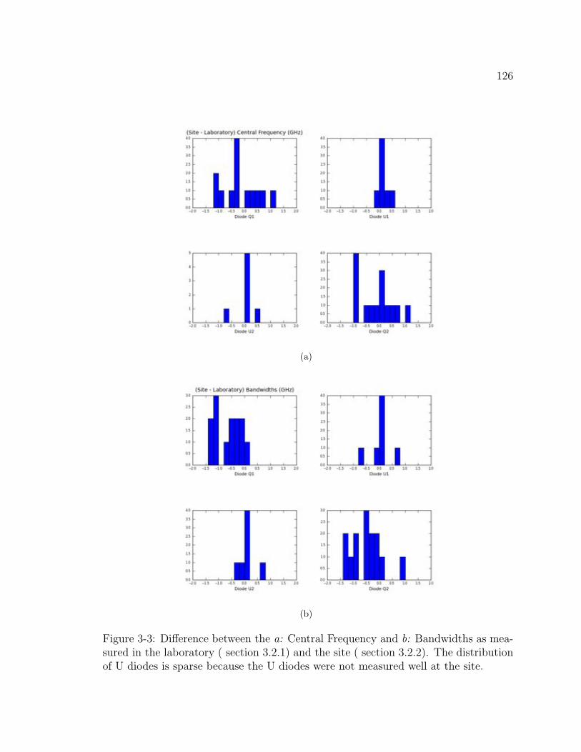
126
(a)
(b)
Figure 3-3: Difference between the a: Central Frequency and b: Bandwidths as mea-sured in the laboratory ( section 3.2.1) and the site ( section 3.2.2). The distributionof U diodes is sparse because the U diodes were not measured well at the site.
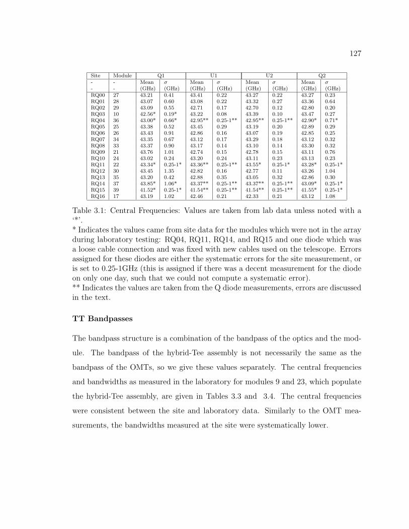
127
Site Module Q1 U1 U2 Q2
- - Mean σ Mean σ Mean σ Mean σ- - (GHz) (GHz) (GHz) (GHz) (GHz) (GHz) (GHz) (GHz)
RQ00 27 43.21 0.41 43.41 0.22 43.27 0.22 43.27 0.23
RQ01 28 43.07 0.60 43.08 0.22 43.32 0.27 43.36 0.64
RQ02 29 43.09 0.55 42.71 0.17 42.70 0.12 42.80 0.20
RQ03 10 42.56* 0.19* 43.22 0.08 43.39 0.10 43.47 0.27
RQ04 36 43.00* 0.66* 42.95** 0.25-1** 42.95** 0.25-1** 42.90* 0.71*
RQ05 25 43.38 0.52 43.45 0.29 43.19 0.20 42.89 0.29
RQ06 26 43.43 0.91 42.86 0.16 43.07 0.19 42.85 0.25
RQ07 34 43.35 0.67 43.12 0.17 43.29 0.18 43.12 0.32
RQ08 33 43.37 0.90 43.17 0.14 43.10 0.14 43.30 0.32
RQ09 21 43.76 1.01 42.74 0.15 42.78 0.15 43.11 0.76
RQ10 24 43.02 0.24 43.20 0.24 43.11 0.23 43.13 0.23
RQ11 22 43.34* 0.25-1* 43.36** 0.25-1** 43.55* 0.25-1* 43.28* 0.25-1*
RQ12 30 43.45 1.35 42.82 0.16 42.77 0.11 43.26 1.04
RQ13 35 43.20 0.42 42.88 0.35 43.05 0.32 42.86 0.30
RQ14 37 43.85* 1.06* 43.37** 0.25-1** 43.37** 0.25-1** 43.09* 0.25-1*
RQ15 39 41.52* 0.25-1* 41.54** 0.25-1** 41.54** 0.25-1** 41.55* 0.25-1*
RQ16 17 43.19 1.02 42.46 0.21 42.33 0.21 43.12 1.08
Table 3.1: Central Frequencies: Values are taken from lab data unless noted with a‘*’.* Indicates the values came from site data for the modules which were not in the arrayduring laboratory testing: RQ04, RQ11, RQ14, and RQ15 and one diode which wasa loose cable connection and was fixed with new cables used on the telescope. Errorsassigned for these diodes are either the systematic errors for the site measurement, oris set to 0.25-1GHz (this is assigned if there was a decent measurement for the diodeon only one day, such that we could not compute a systematic error).** Indicates the values are taken from the Q diode measurements, errors are discussedin the text.
TT Bandpasses
The bandpass structure is a combination of the bandpass of the optics and the mod-
ule. The bandpass of the hybrid-Tee assembly is not necessarily the same as the
bandpass of the OMTs, so we give these values separately. The central frequencies
and bandwidths as measured in the laboratory for modules 9 and 23, which populate
the hybrid-Tee assembly, are given in Tables 3.3 and 3.4. The central frequencies
were consistent between the site and laboratory data. Similarly to the OMT mea-
surements, the bandwidths measured at the site were systematically lower.
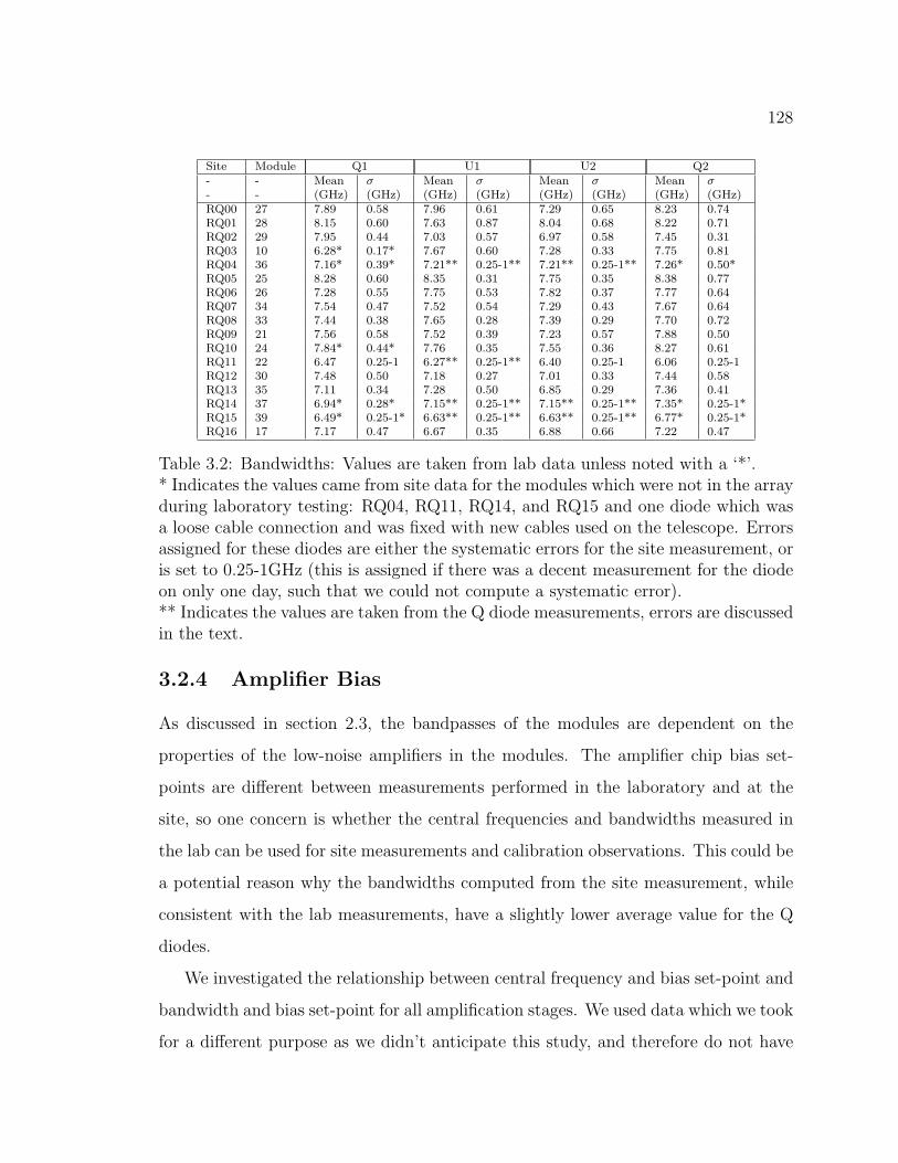
128
Site Module Q1 U1 U2 Q2
- - Mean σ Mean σ Mean σ Mean σ- - (GHz) (GHz) (GHz) (GHz) (GHz) (GHz) (GHz) (GHz)
RQ00 27 7.89 0.58 7.96 0.61 7.29 0.65 8.23 0.74
RQ01 28 8.15 0.60 7.63 0.87 8.04 0.68 8.22 0.71
RQ02 29 7.95 0.44 7.03 0.57 6.97 0.58 7.45 0.31
RQ03 10 6.28* 0.17* 7.67 0.60 7.28 0.33 7.75 0.81
RQ04 36 7.16* 0.39* 7.21** 0.25-1** 7.21** 0.25-1** 7.26* 0.50*
RQ05 25 8.28 0.60 8.35 0.31 7.75 0.35 8.38 0.77
RQ06 26 7.28 0.55 7.75 0.53 7.82 0.37 7.77 0.64
RQ07 34 7.54 0.47 7.52 0.54 7.29 0.43 7.67 0.64
RQ08 33 7.44 0.38 7.65 0.28 7.39 0.29 7.70 0.72
RQ09 21 7.56 0.58 7.52 0.39 7.23 0.57 7.88 0.50
RQ10 24 7.84* 0.44* 7.76 0.35 7.55 0.36 8.27 0.61
RQ11 22 6.47 0.25-1 6.27** 0.25-1** 6.40 0.25-1 6.06 0.25-1
RQ12 30 7.48 0.50 7.18 0.27 7.01 0.33 7.44 0.58
RQ13 35 7.11 0.34 7.28 0.50 6.85 0.29 7.36 0.41
RQ14 37 6.94* 0.28* 7.15** 0.25-1** 7.15** 0.25-1** 7.35* 0.25-1*
RQ15 39 6.49* 0.25-1* 6.63** 0.25-1** 6.63** 0.25-1** 6.77* 0.25-1*
RQ16 17 7.17 0.47 6.67 0.35 6.88 0.66 7.22 0.47
Table 3.2: Bandwidths: Values are taken from lab data unless noted with a ‘*’.* Indicates the values came from site data for the modules which were not in the arrayduring laboratory testing: RQ04, RQ11, RQ14, and RQ15 and one diode which wasa loose cable connection and was fixed with new cables used on the telescope. Errorsassigned for these diodes are either the systematic errors for the site measurement, oris set to 0.25-1GHz (this is assigned if there was a decent measurement for the diodeon only one day, such that we could not compute a systematic error).** Indicates the values are taken from the Q diode measurements, errors are discussedin the text.
3.2.4 Amplifier Bias
As discussed in section 2.3, the bandpasses of the modules are dependent on the
properties of the low-noise amplifiers in the modules. The amplifier chip bias set-
points are different between measurements performed in the laboratory and at the
site, so one concern is whether the central frequencies and bandwidths measured in
the lab can be used for site measurements and calibration observations. This could be
a potential reason why the bandwidths computed from the site measurement, while
consistent with the lab measurements, have a slightly lower average value for the Q
diodes.
We investigated the relationship between central frequency and bias set-point and
bandwidth and bias set-point for all amplification stages. We used data which we took
for a different purpose as we didn’t anticipate this study, and therefore do not have
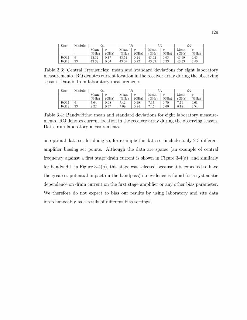
129
Site Module Q1 U1 U2 Q2
- - Mean σ Mean σ Mean σ Mean σ- - (GHz) (GHz) (GHz) (GHz) (GHz) (GHz) (GHz) (GHz)
RQ17 9 43.32 0.17 43.52 0.24 43.62 0.03 43.69 0.43
RQ18 23 43.38 0.34 43.09 0.22 43.32 0.23 43.53 0.40
Table 3.3: Central Frequencies: mean and standard deviations for eight laboratorymeasurements. RQ denotes current location in the receiver array during the observingseason. Data is from laboratory measurements.
Site Module Q1 U1 U2 Q2
- - Mean σ Mean σ Mean σ Mean σ- - (GHz) (GHz) (GHz) (GHz) (GHz) (GHz) (GHz) (GHz)
RQ17 9 7.64 0.68 7.42 0.49 7.17 0.70 7.79 0.61
RQ18 23 8.22 0.47 7.69 0.84 7.45 0.66 8.18 0.54
Table 3.4: Bandwidths: mean and standard deviations for eight laboratory measure-ments. RQ denotes current location in the receiver array during the observing season.Data from laboratory measurements.
an optimal data set for doing so, for example the data set includes only 2-3 different
amplifier biasing set points. Although the data are sparse (an example of central
frequency against a first stage drain current is shown in Figure 3-4(a), and similarly
for bandwidth in Figure 3-4(b), this stage was selected because it is expected to have
the greatest potential impact on the bandpass) no evidence is found for a systematic
dependence on drain current on the first stage amplifier or any other bias parameter.
We therefore do not expect to bias our results by using laboratory and site data
interchangeably as a result of different bias settings.
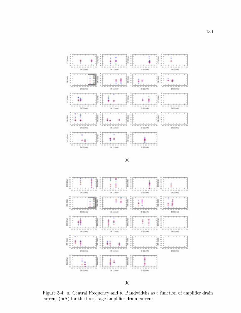
130
(a)
(b)
Figure 3-4: a: Central Frequency and b: Bandwidths as a function of amplifier draincurrent (mA) for the first stage amplifier drain current.
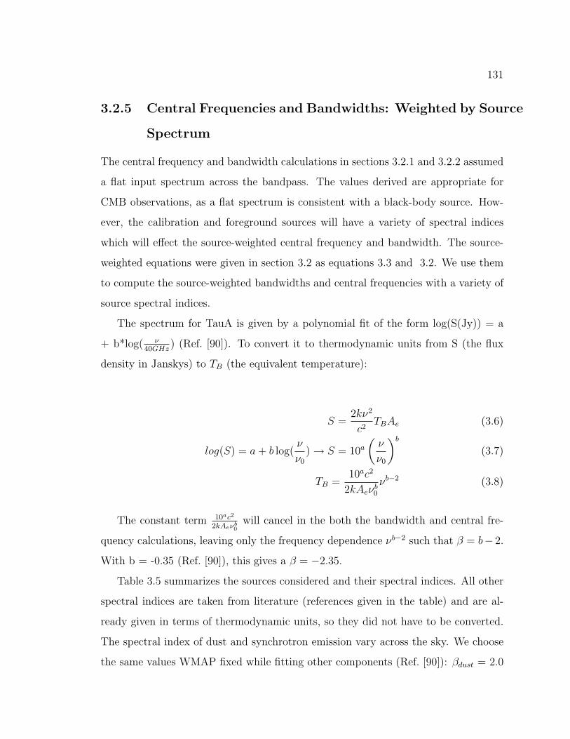
131
3.2.5 Central Frequencies and Bandwidths: Weighted by Source
Spectrum
The central frequency and bandwidth calculations in sections 3.2.1 and 3.2.2 assumed
a flat input spectrum across the bandpass. The values derived are appropriate for
CMB observations, as a flat spectrum is consistent with a black-body source. How-
ever, the calibration and foreground sources will have a variety of spectral indices
which will effect the source-weighted central frequency and bandwidth. The source-
weighted equations were given in section 3.2 as equations 3.3 and 3.2. We use them
to compute the source-weighted bandwidths and central frequencies with a variety of
source spectral indices.
The spectrum for TauA is given by a polynomial fit of the form log(S(Jy)) = a
+ b*log( ν40GHz ) (Ref. [90]). To convert it to thermodynamic units from S (the flux
density in Janskys) to TB (the equivalent temperature):
S =2kν
2
c2TBAe (3.6)
log(S) = a + b log(ν
ν0
) → S = 10a
ν
ν0
b
(3.7)
TB =10a
c2
2kAeνb0
νb−2 (3.8)
The constant term 10ac2
2kAeνb0
will cancel in the both the bandwidth and central fre-
quency calculations, leaving only the frequency dependence νb−2 such that β = b− 2.
With b = -0.35 (Ref. [90]), this gives a β = −2.35.
Table 3.5 summarizes the sources considered and their spectral indices. All other
spectral indices are taken from literature (references given in the table) and are al-
ready given in terms of thermodynamic units, so they did not have to be converted.
The spectral index of dust and synchrotron emission vary across the sky. We choose
the same values WMAP fixed while fitting other components (Ref. [90]): βdust = 2.0
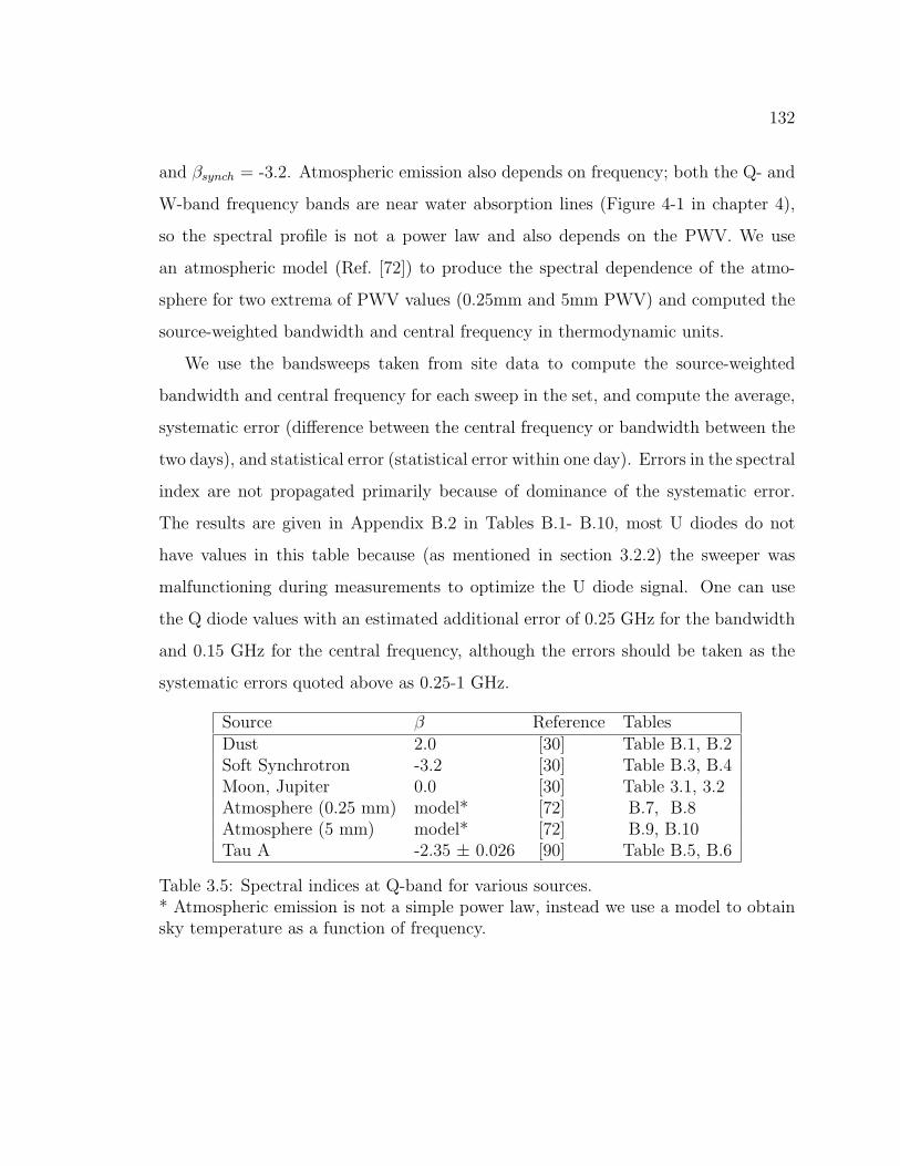
132
and βsynch = -3.2. Atmospheric emission also depends on frequency; both the Q- and
W-band frequency bands are near water absorption lines (Figure 4-1 in chapter 4),
so the spectral profile is not a power law and also depends on the PWV. We use
an atmospheric model (Ref. [72]) to produce the spectral dependence of the atmo-
sphere for two extrema of PWV values (0.25mm and 5mm PWV) and computed the
source-weighted bandwidth and central frequency in thermodynamic units.
We use the bandsweeps taken from site data to compute the source-weighted
bandwidth and central frequency for each sweep in the set, and compute the average,
systematic error (difference between the central frequency or bandwidth between the
two days), and statistical error (statistical error within one day). Errors in the spectral
index are not propagated primarily because of dominance of the systematic error.
The results are given in Appendix B.2 in Tables B.1- B.10, most U diodes do not
have values in this table because (as mentioned in section 3.2.2) the sweeper was
malfunctioning during measurements to optimize the U diode signal. One can use
the Q diode values with an estimated additional error of 0.25 GHz for the bandwidth
and 0.15 GHz for the central frequency, although the errors should be taken as the
systematic errors quoted above as 0.25-1 GHz.
Source β Reference TablesDust 2.0 [30] Table B.1, B.2Soft Synchrotron -3.2 [30] Table B.3, B.4Moon, Jupiter 0.0 [30] Table 3.1, 3.2Atmosphere (0.25 mm) model* [72] B.7, B.8Atmosphere (5 mm) model* [72] B.9, B.10Tau A -2.35 ± 0.026 [90] Table B.5, B.6
Table 3.5: Spectral indices at Q-band for various sources.* Atmospheric emission is not a simple power law, instead we use a model to obtainsky temperature as a function of frequency.
133
3.3 Noise Temperature Measurements
Receiver noise can be computed via a ‘Y-factor’ measurement. This measurement
uses two black-body thermal loads at two different temperatures (Thot and Tcold) to
isolate the contribution from receiver noise (Treceiver) to the power measured by the
detector as:
Treceiver =Thot − Y Tcold
Y − 1(3.9)
where
Y =Phot
Pcold(3.10)
Phot is the average power (as discussed in section 2.3.2, the detector diode output of
the QUIET modules in Volts is proportional to power, so in practice the average power
will be the average voltage measured by a detector diode) detected while looking at
a thermal load at temperature Thot, and Pcold is the equivalent for a thermal load
at temperature Tcold. We used three thermal loads, each consisting of a Zotefoam1
(closed-cell expanded polypropylene foam) container with an absorber insert. One
load was kept at room temperature (absorber temperature 300 K), the other two
loads were filled with liquid cryogens: one with liquid nitrogen (absorber temperature
77.5 K) and one with liquid oxygen (absorber temperature 90 K). The two cryogenic
loads were placed on a cart (Figure 3-5) such that the window of the cryostat could
‘stare’ into the thermal load.
Zotefoam is >99% transparent at microwave frequencies (Ref. [15]) such that the
modules observe a signal primarily from the absorber. With three load temperatures
we obtain three Y-factor measurements of the receiver noise (Thot=300 K, Tcold=90 K;
1http:zotefoams.com
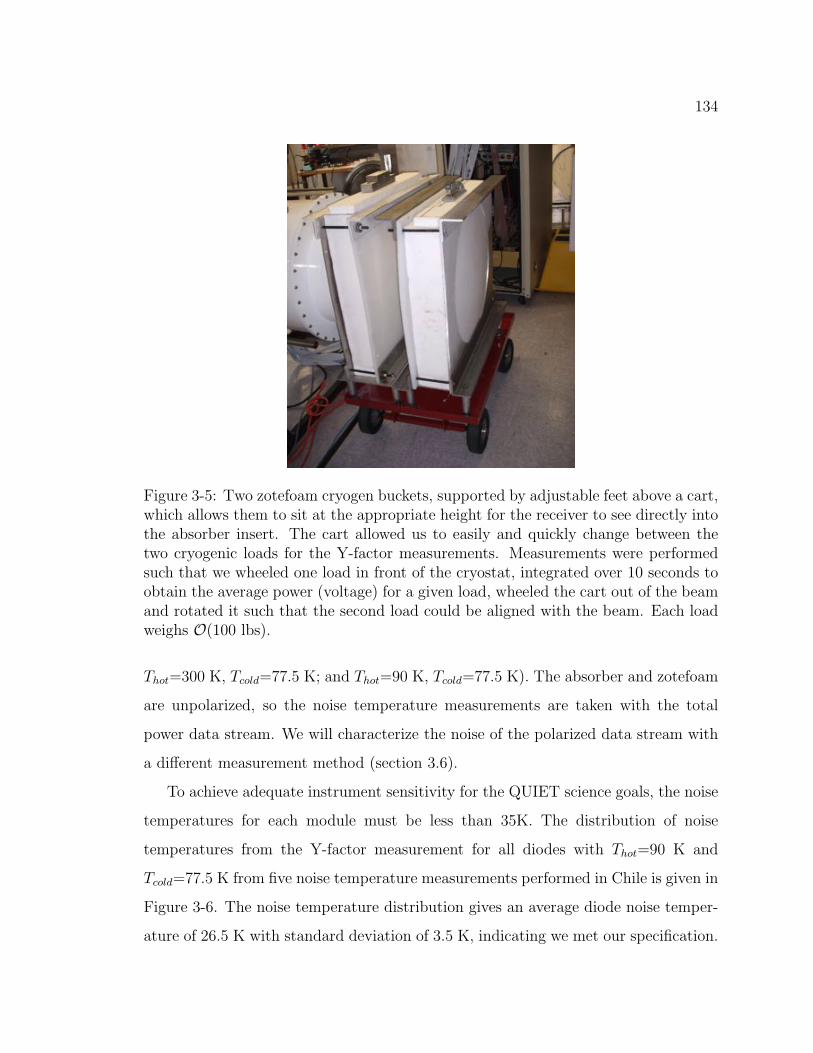
134
Figure 3-5: Two zotefoam cryogen buckets, supported by adjustable feet above a cart,which allows them to sit at the appropriate height for the receiver to see directly intothe absorber insert. The cart allowed us to easily and quickly change between thetwo cryogenic loads for the Y-factor measurements. Measurements were performedsuch that we wheeled one load in front of the cryostat, integrated over 10 seconds toobtain the average power (voltage) for a given load, wheeled the cart out of the beamand rotated it such that the second load could be aligned with the beam. Each loadweighs O(100 lbs).
Thot=300 K, Tcold=77.5 K; and Thot=90 K, Tcold=77.5 K). The absorber and zotefoam
are unpolarized, so the noise temperature measurements are taken with the total
power data stream. We will characterize the noise of the polarized data stream with
a different measurement method (section 3.6).
To achieve adequate instrument sensitivity for the QUIET science goals, the noise
temperatures for each module must be less than 35K. The distribution of noise
temperatures from the Y-factor measurement for all diodes with Thot=90 K and
Tcold=77.5 K from five noise temperature measurements performed in Chile is given in
Figure 3-6. The noise temperature distribution gives an average diode noise temper-
ature of 26.5 K with standard deviation of 3.5 K, indicating we met our specification.
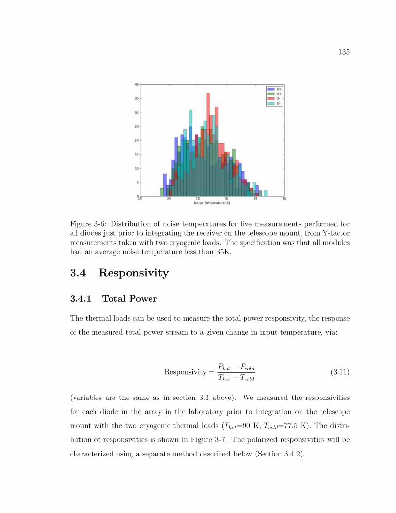
135
Figure 3-6: Distribution of noise temperatures for five measurements performed forall diodes just prior to integrating the receiver on the telescope mount, from Y-factormeasurements taken with two cryogenic loads. The specification was that all moduleshad an average noise temperature less than 35K.
3.4 Responsivity
3.4.1 Total Power
The thermal loads can be used to measure the total power responsivity, the response
of the measured total power stream to a given change in input temperature, via:
Responsivity =Phot − Pcold
Thot − Tcold(3.11)
(variables are the same as in section 3.3 above). We measured the responsivities
for each diode in the array in the laboratory prior to integration on the telescope
mount with the two cryogenic thermal loads (Thot=90 K, Tcold=77.5 K). The distri-
bution of responsivities is shown in Figure 3-7. The polarized responsivities will be
characterized using a separate method described below (Section 3.4.2).
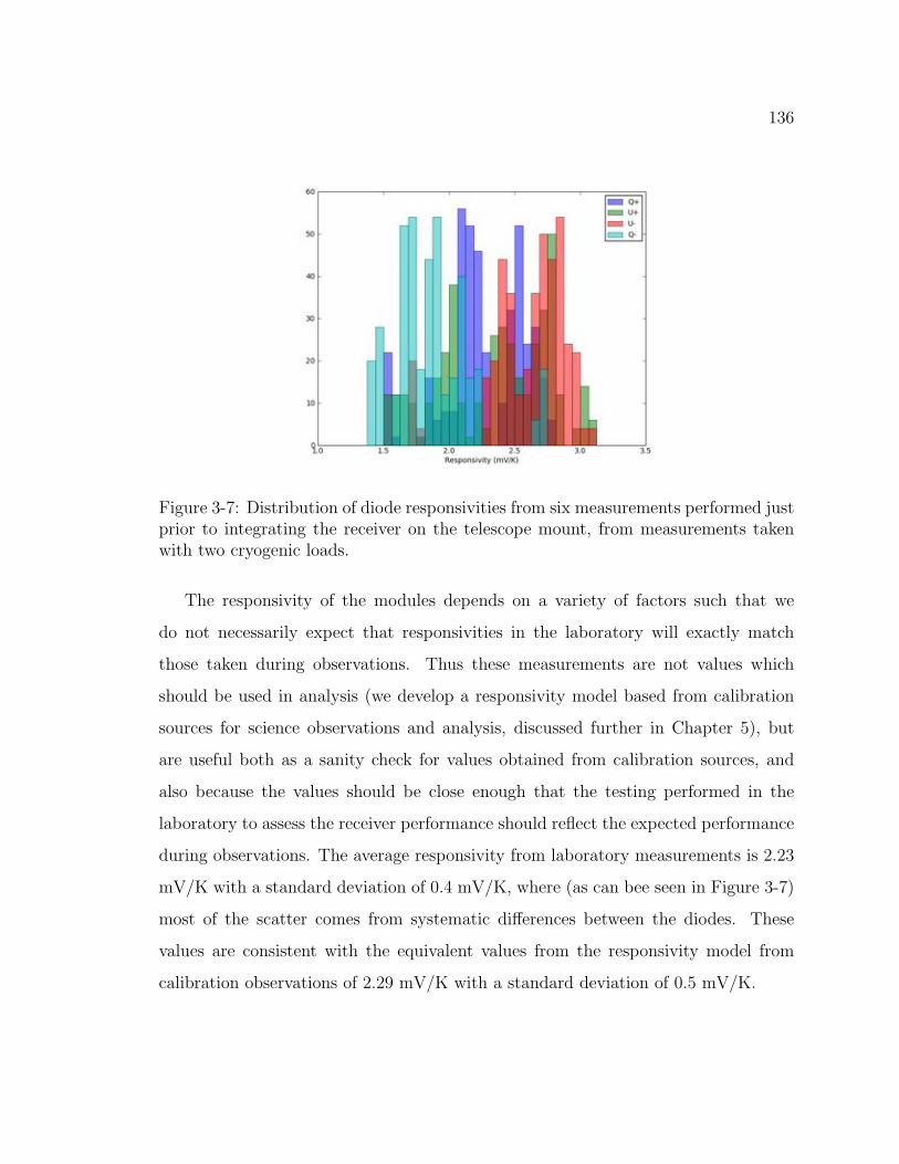
136
Figure 3-7: Distribution of diode responsivities from six measurements performed justprior to integrating the receiver on the telescope mount, from measurements takenwith two cryogenic loads.
The responsivity of the modules depends on a variety of factors such that we
do not necessarily expect that responsivities in the laboratory will exactly match
those taken during observations. Thus these measurements are not values which
should be used in analysis (we develop a responsivity model based from calibration
sources for science observations and analysis, discussed further in Chapter 5), but
are useful both as a sanity check for values obtained from calibration sources, and
also because the values should be close enough that the testing performed in the
laboratory to assess the receiver performance should reflect the expected performance
during observations. The average responsivity from laboratory measurements is 2.23
mV/K with a standard deviation of 0.4 mV/K, where (as can bee seen in Figure 3-7)
most of the scatter comes from systematic differences between the diodes. These
values are consistent with the equivalent values from the responsivity model from
calibration observations of 2.29 mV/K with a standard deviation of 0.5 mV/K.
137
3.4.2 Polarized Response
We measured the polarized response of the receiver with the ‘optimizer’, a reflective
plate and cryogenic load system that rotates around the boresight of the cryostat
(schematic shown in Figure 3-8(a) and a picture in Figure 3-8(b)). The plate is
oriented at angle β from the horizontal and reflects the light from the cryogenic load
into the window of the cryostat with a small polarization defined by the resistivity
and temperature of the plate, the plate angle β, and the temperature of the load.
This entire apparatus rotates at a rate α such that the resulting polarized signal will
rotate between the Stokes vectors at a rate of 2α. Polarization signals which do not
rotate with the system (such as thermal emission from objects in the lab, which will
also reflect from the plate and into the cryostat) will be detected at a rate of α, thus
these effects can be removed. The loads were too small to fill the entire array beam,
so the measurements are only used from the central polarimeter. This will still allow
us to verify that the total power and polarized responsivities are similar, which will
allow us to use total power gains when assessing polarized instrument sensitivity (see
section 3.7).
Using the resistivity of a given reflector plate material and temperature of the
thermal load, we can calculate the the magnitude of the polarized emission as equa-
tion 3.12 (derived in appendix C).
138
(a) (b)
Figure 3-8: a: The optimizer consists of a reflective metal plate and a cryogenic load.The reflected signal is polarized (given by equation 3.12), as thermal load and plate arerotated around the cryostat window, the polarized signal will rotate. The stationarymodule will have a polarization axis, in this case noted as x and y in the figure. Asthe polarized signal rotates between x and y, the module will observe this as changingvoltage levels on the Q and U diodes. Courtesy Keith Vanderlinde. b: A photographof the optimizer setup on top of the Q-band cryostat. The cryogenic thermal load(white circular aperture) is one of the zotefoam buckets shown in Figure 3-5, thesignal is reflected off of a metal plate (in profile) and into the window of the cryostat.Each load is 2 ft tall. Courtesy Ross Williamson.
139
I =
4πνρ0(cos(β)− sec(β))(Tplate − Tload) sin(2α) (3.12)
The predicted polarized emission and the measured voltage on the detector diodes
give us the polarized reponsivity for the central polarimeter. We used multiple plate
materials and two thermal loads to obtain multiple estimates of the responsivity. The
theoretically predicted polarization for each plate and cryogenic load temperature are
given in Table 3.6.
Cryogen Material Resistivity Signal (mK)LN2 Aluminum 2.9×10⁻⁸ 54LN2 Stainless Steel 7.2×10⁻⁷ 267LO2 Aluminum 2.9×10⁻⁸ 51LO2 Stainless Steel 7.2×10⁻⁷ 250
Table 3.6: Expected polarized emission from the optimizer with different metal platesand cryogen loads. Assumed plate temperature is 289K and plate is at an angleβ = 45 from the horizontal. Courtesy Ross Williamson.
An example of the measured signal from the optimizer for one of the diodes in the
central module is given in Figure 3-9, the sinusoidal portion of the plot corresponds
to rotation of the optimizer assembly around the cryostat boresight. The sinusoidal
measurement was fit with equation 3.13:
f(t) = C0 sin(ωt + c0) + C1 sin(2ωt + c1) + C2 (3.13)
We extract the amplitude of the signal modulated at 2ω (coefficient C1) and
calculate the polarized responsivity from equation 3.12 given the known temperature
of the load, the temperature and the resistivity of the metal plate. A comparison
between the total power responsivity, measured with the two cryogenic thermal loads
prior to setting up the optimizer, and the polarized responsivity measured with the
140
Figure 3-9: An example time stream of signal from an optimizer measurement forthe Q+ diode (D1) with liquid nitrogen as the thermal load and the stainless steelplate as the metal reflector. The first section of data around 0V is taken with thephase switches biased down to give an offset measurement. The sinusoidal curvecorresponds to rotating the plate and thermal load around the cryostat boresight,and the constant segment at the end was used to obtain the white noise. CourtesyRoss Williamson.
optimizer is shown in Figure 3-10. We show only measurements from the stainless
steel plate because the signal-to-noise ratio for the aluminum plate measurement
was too low to yield reliable results. The polarized responsivity is consistent with
the total power responsivity for the central polarimeter. This is consistent with
calibration measurements taken during observations in Chile (section 5.3), which
found comparable responsivities between the total power and demodulated streams.
3.5 Compression
The responsivity calculation assumes that the power measured by the modules is
linear across the range of input thermal loads. As discussed in Section 2.3, the third
141
Figure 3-10: A comparison between the total power and polarized gains for the centralpolarimeter, all diodes. The green line indicates unity such that the total power andpolarized gains are identical. The total power gain values used are the same for allloads and plate materials, as it was obtained from a previous measurement. We donot have estimates of error for this measurement. The responsivity of this modulefrom analysis of calibration data taken during observations are consistent with thesevalues (polarized responsivities of 1.7-2.9 mV/K).
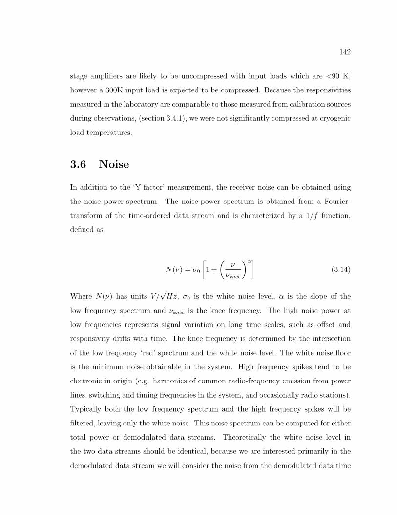
142
stage amplifiers are likely to be uncompressed with input loads which are <90 K,
however a 300K input load is expected to be compressed. Because the responsivities
measured in the laboratory are comparable to those measured from calibration sources
during observations, (section 3.4.1), we were not significantly compressed at cryogenic
load temperatures.
3.6 Noise
In addition to the ‘Y-factor’ measurement, the receiver noise can be obtained using
the noise power-spectrum. The noise-power spectrum is obtained from a Fourier-
transform of the time-ordered data stream and is characterized by a 1/f function,
defined as:
N(ν) = σ0
1 +
ν
νknee
α(3.14)
Where N(ν) has units V/√
Hz, σ0 is the white noise level, α is the slope of the
low frequency spectrum and νknee is the knee frequency. The high noise power at
low frequencies represents signal variation on long time scales, such as offset and
responsivity drifts with time. The knee frequency is determined by the intersection
of the low frequency ‘red’ spectrum and the white noise level. The white noise floor
is the minimum noise obtainable in the system. High frequency spikes tend to be
electronic in origin (e.g. harmonics of common radio-frequency emission from power
lines, switching and timing frequencies in the system, and occasionally radio stations).
Typically both the low frequency spectrum and the high frequency spikes will be
filtered, leaving only the white noise. This noise spectrum can be computed for either
total power or demodulated data streams. Theoretically the white noise level in
the two data streams should be identical, because we are interested primarily in the
demodulated data stream we will consider the noise from the demodulated data time
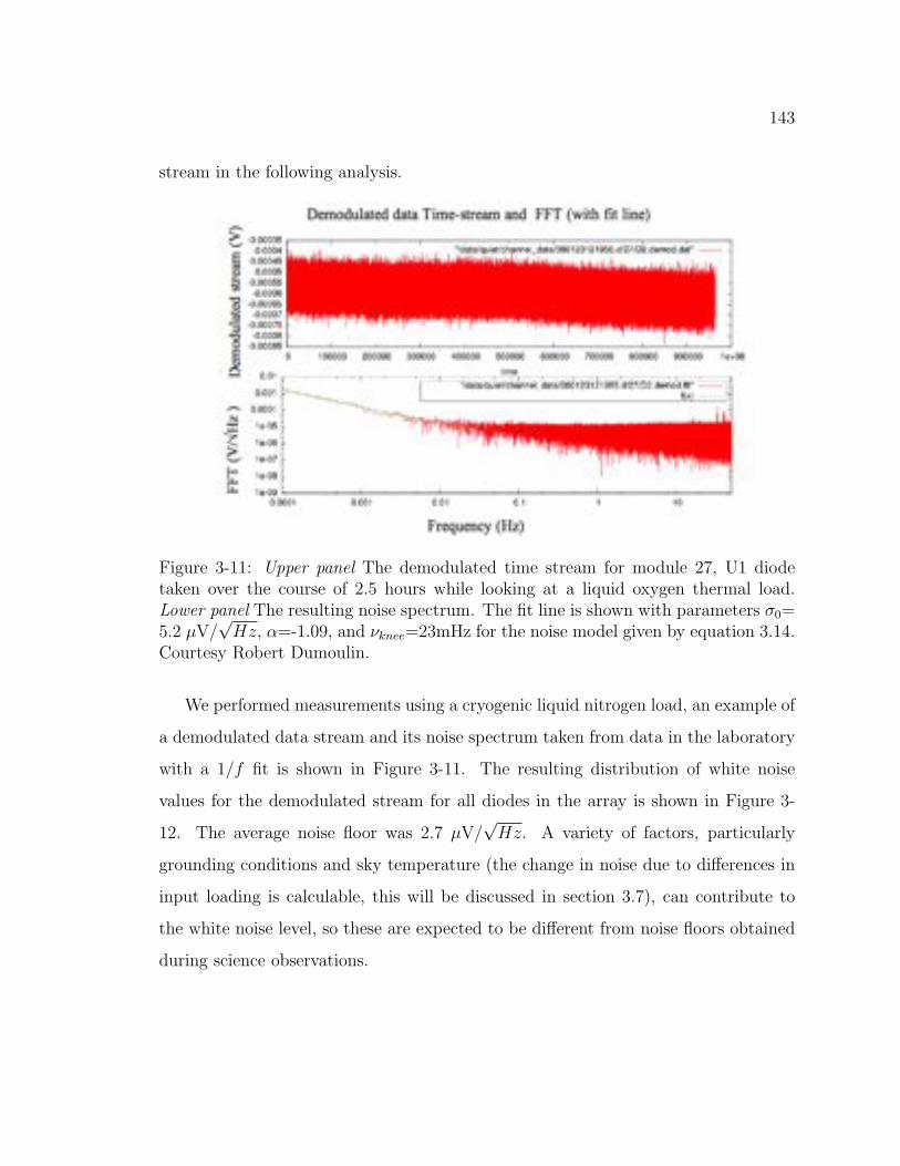
143
stream in the following analysis.
Figure 3-11: Upper panel The demodulated time stream for module 27, U1 diodetaken over the course of 2.5 hours while looking at a liquid oxygen thermal load.Lower panel The resulting noise spectrum. The fit line is shown with parameters σ0=5.2 µV/
√Hz, α=-1.09, and νknee=23mHz for the noise model given by equation 3.14.
Courtesy Robert Dumoulin.
We performed measurements using a cryogenic liquid nitrogen load, an example of
a demodulated data stream and its noise spectrum taken from data in the laboratory
with a 1/f fit is shown in Figure 3-11. The resulting distribution of white noise
values for the demodulated stream for all diodes in the array is shown in Figure 3-
12. The average noise floor was 2.7 µV/√
Hz. A variety of factors, particularly
grounding conditions and sky temperature (the change in noise due to differences in
input loading is calculable, this will be discussed in section 3.7), can contribute to
the white noise level, so these are expected to be different from noise floors obtained
during science observations.
144
Figure 3-12: Distribution of white noise floor values for measurements just prior tointegrating the receiver on the telescope mount, from a liquid-nitrogen stare over onehour with the demodulated stream.
3.7 Instrument Sensitivity
We chose the size of the pathfinder arrays to significantly improve E-mode mea-
surements and B-mode constraints, and to prove the technology for future Phase II
B-mode searches. Measurements were performed in the laboratory in Chile prior to
science observations to verify that the receiver array would have an on-sky sensitivity
better than 60µKs1/2 (per-horn sensitivity of 300µKs
1/2).
We compute polarimeter sensitivity with two different formulae. One method
uses the noise temperatures calculated from a Y-factor measurement and receiver
bandwidth to tabulate the sensitivity via:
145
Sensitivity ≡Treceiver + Tinput load
√∆ν
Ks
1/2
(3.15)
The second method uses a measurement of the white noise obtained while looking at
a cryogenic load for 1 hour with the responsivity obtained from the two cryogenic
loads to compute the sensitivity via:
Sensitivity ≡noise
responsivity
Vs
1/2
V/K= Ks
1/2
(3.16)
The first method will yield a measurement of the sensitivity for the total power
stream. The second method can be used as measurement of the polarized sensitiv-
ity under the assumption that the total power and demodulated responsivitites are
identical (verified by measurements given in section 3.4.2, and also shown to be true
in the responsivity derived from calibration measurements during the observing sea-
son given in section 5). The distributions of the sensitivity for each diode for both
calculations is given in Figure 3-13; the two methods of computing the sensitivity
are comparable, indicating that the measurements of noise, gain, and bandwidth are
consistent and also that the noise and gain between the demodulated and total power
data streams are consistent.
The sensitivity for the entire array was computed as:
Array sensitivity (K s1/2) =
diode S
2
diode
Ndiodes(3.17)
The array sensitivity values were obtained from both methodologies, and extrap-
olated to the Chilean sky temperature. This conversion is detailed thoroughly in
appendix D, and includes the following:
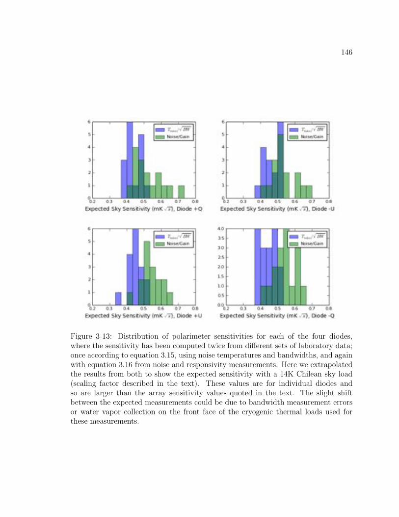
146
Figure 3-13: Distribution of polarimeter sensitivities for each of the four diodes,where the sensitivity has been computed twice from different sets of laboratory data;once according to equation 3.15, using noise temperatures and bandwidths, and againwith equation 3.16 from noise and responsivity measurements. Here we extrapolatedthe results from both to show the expected sensitivity with a 14K Chilean sky load(scaling factor described in the text). These values are for individual diodes andso are larger than the array sensitivity values quoted in the text. The slight shiftbetween the expected measurements could be due to bandwidth measurement errorsor water vapor collection on the front face of the cryogenic thermal loads used forthese measurements.
147
• Noise is a function of input thermal load, so we must include a scaling factor
Csky between the cryogenic loads used and the Chilean sky temperature. We do
not have an exact measurement for the sky temperature, so it is not surprising
if the extrapolated sensitivity from laboratory measurements do not exactly
match those found from observations.
• As presented in appendix D, we must include a correction for the Rayleigh-Jeans
approximation for the black-body loads, CRJ .
• We mask data around the phase switch transition region, this removes 13% of
the data, and this factor must be included in equation 3.15. This masking factor
Cmask was first discussed in section 2.5, and is treated in appendix D.
The final result is:
Sensitivity = CRJ CskyTreceiver + Tsky√
∆ν ∗ Cmask
(3.18)
Sensitivity = CRJ Cskynoise
gain(3.19)
The atmospheric model we use for QUIET (Ref. [72]) predicts a zenith temper-
ature of 8.5K, our range of observing elevations (70 to 43) will yield atmospheric
temperatures between 9K and 12.5K. I will assume a sky temperature of 11K, includ-
ing the 3K CMB contribution, the total sky temperature is 14K. Accounting for
the module which broke just prior to integration on the deck, the extrapolated array
sensitivity values are 56 µKs1/2 and 68 µKs
1/2 for equation 3.15 and equation 3.16,
respectively. Taking the worst of the two values, we nearly achieved our sensitivity
goal of 60 µKs1/2. Values from science data from observations indicate an average
array sensitivity value of 60 µKs1/2 (Chapter 5), computed via 3.16.
Chapter 4
Summary of Q-band Season:
Observations and Data Reduction
This chapter addresses the QUIET observing site, observations with the Q-band
receiver, data selection, and data reduction. QUIET observations are performed from
the Chajnantor Test Facility (CTF). Between July and September 2008, the Q-band
receiver was deployed to the CTF and calibration and commissioning observations
were performed. Science data were collected between October 2008 and June 2009,
during which time over 3000 hours of CMB data were logged. The Q-band receiver
was removed from the telescope and replaced by the W-band receiver in June 2009.
W-band observations are currently underway.
4.1 QUIET Observing Site
4.1.1 Observing Conditions
Microwave and sub-millimeter experiments select very dry observing sites to reduce
signal absorption by atmospheric water vapor, and high altitude sites to reduce ab-
sorption from oxygen. The CTF is located at an altitude of 5080 m in the Atacama
148
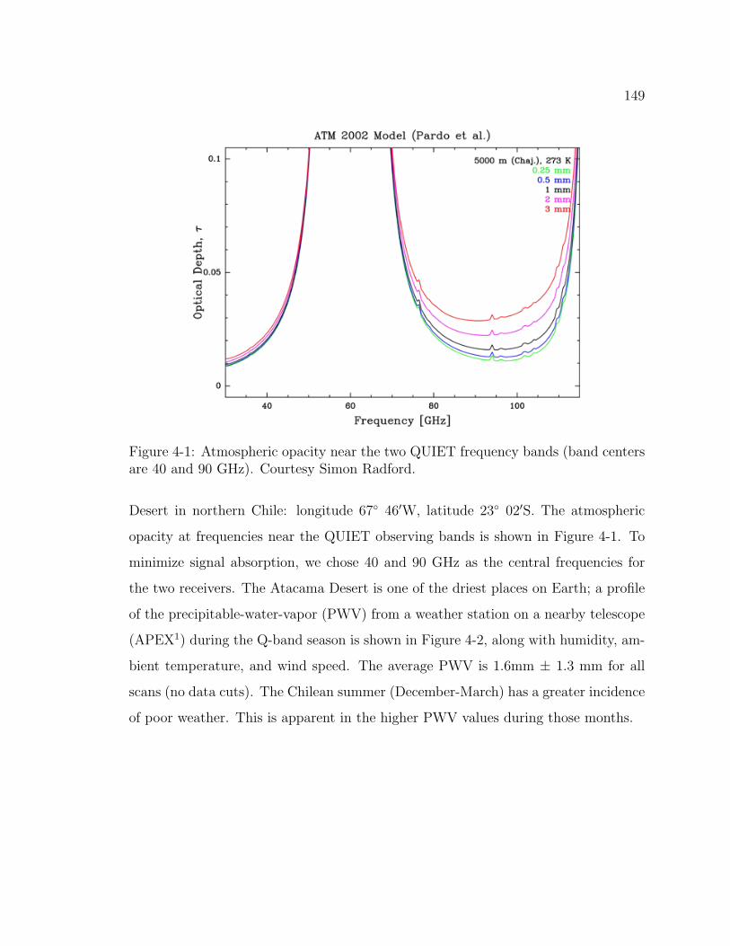
149
Figure 4-1: Atmospheric opacity near the two QUIET frequency bands (band centersare 40 and 90 GHz). Courtesy Simon Radford.
Desert in northern Chile: longitude 67 46W, latitude 23 02S. The atmospheric
opacity at frequencies near the QUIET observing bands is shown in Figure 4-1. To
minimize signal absorption, we chose 40 and 90 GHz as the central frequencies for
the two receivers. The Atacama Desert is one of the driest places on Earth; a profile
of the precipitable-water-vapor (PWV) from a weather station on a nearby telescope
(APEX1) during the Q-band season is shown in Figure 4-2, along with humidity, am-
bient temperature, and wind speed. The average PWV is 1.6mm ± 1.3 mm for all
scans (no data cuts). The Chilean summer (December-March) has a greater incidence
of poor weather. This is apparent in the higher PWV values during those months.
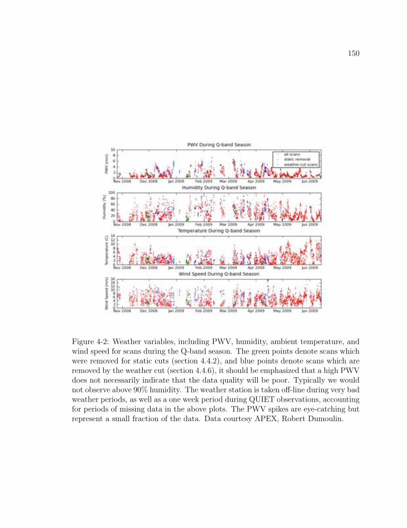
150
Figure 4-2: Weather variables, including PWV, humidity, ambient temperature, andwind speed for scans during the Q-band season. The green points denote scans whichwere removed for static cuts (section 4.4.2), and blue points denote scans which areremoved by the weather cut (section 4.4.6), it should be emphasized that a high PWVdoes not necessarily indicate that the data quality will be poor. Typically we wouldnot observe above 90% humidity. The weather station is taken off-line during very badweather periods, as well as a one week period during QUIET observations, accountingfor periods of missing data in the above plots. The PWV spikes are eye-catching butrepresent a small fraction of the data. Data courtesy APEX, Robert Dumoulin.
151
4.2 Patch Selection
We selected four CMB patches (2a, 4a, 6a, 7b) and two Galactic patches (Gb, Gc),
each covering 15 × 15, for observations. The QUIET patch coordinates are shown
in Figure 4-3(a) and given in Table 4-3(b). QUIET patches were selected for their
low synchrotron emission as measured by WMAP and because they remain at least
30 from the Sun and Moon during the year, allowing uninterrupted observations
throughout the season. The two patches with the least expected foreground contam-
ination are 4a and 6a. These patches were prioritized for scan time over the other
patches.
4.3 Scan Strategy
QUIET primarily observes at four deck angles during the observing season: 30,
75, 120, 165. Stepping the deck angle by 45 rotates the Stokes Q into Stokes U
parameters.
We employ a fixed-elevation, azimuth-scanning technique: a patch is scanned in
azimuth as it drifts through the beam, which generally takes 1.5 hours. The tele-
scope then re-tracks the patch and begins another scan. By scanning at constant
elevation for a given scan, we observe through a constant column density of atmo-
sphere such that only weather variations within a scan contribute to atmospheric
signal.
4.4 Data Selection and Reduction
Data reduction and analysis are performed on each patch using two independent
pipelines, one employing maximum-likelihood map-making and power spectrum es-
1The Atacama Patchfinder Experiment - a collaboration between the Max-Planck Institut furRadioastronomie of Bonn, the European Southern Observatory, and the Onsala Space Observatory
152
timation (Ref. [26]), and one a Pseudo-C estimator (Ref. [82]). The data used in
science analyses must be clean of artifacts such as weather, polarimeter malfunc-
tions, and ground pickup. Selection criteria were developed independently for each
pipeline from analysis of the time-ordered data stream, spectral information, and map-
based tests. This chapter addresses data selection and reduction for the Maximum-
likelihood pipeline, I will note which cuts are shared between the two pipelines.
4.4.1 Nomenclature
• TOD: Time-ordered Data: Polarimeter data in the time domain (polarime-
ter voltage as a function of time).
• CES by scan and segment: A segment is one full scan of a patch, performed
at a constant elevation. Usually a given patch is within the elevation range of the
telescope for longer than a single segment, so the telescope re-tracks to another
elevation and performs another segment scan. Any segments of the same patch
in series are labelled with the same scan number as the other scans, and is
given a segment number to distinguish it from the scans at other elevations in
the series. The scan and segment number together denote a Constant Elevation
Scan (CES).
4.4.2 Standard and Static Cuts
The baseline data selection (removing dead detector diodes, testing procedures during
the season) is common between the two pipelines. A description of these cuts and
the effected scans is given in Table 4.1. I maintain the distinction between standard
and static cuts for consistency with the notation used by the collaboration, there is
no intrinsic difference.
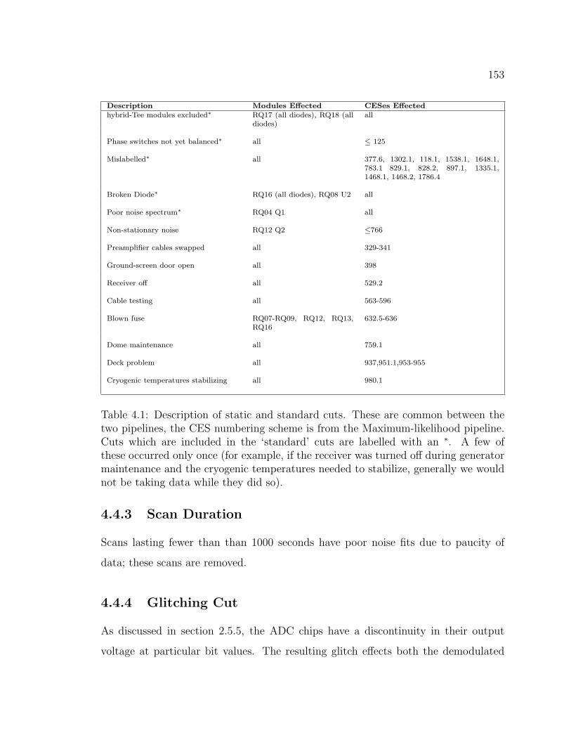
153
Description Modules Effected CESes Effectedhybrid-Tee modules excluded
∗RQ17 (all diodes), RQ18 (all
diodes)
all
Phase switches not yet balanced∗
all ≤ 125
Mislabelled∗
all 377.6, 1302.1, 118.1, 1538.1, 1648.1,
783.1 829.1, 828.2, 897.1, 1335.1,
1468.1, 1468.2, 1786.4
Broken Diode∗
RQ16 (all diodes), RQ08 U2 all
Poor noise spectrum∗
RQ04 Q1 all
Non-stationary noise RQ12 Q2 ≤766
Preamplifier cables swapped all 329-341
Ground-screen door open all 398
Receiver off all 529.2
Cable testing all 563-596
Blown fuse RQ07-RQ09, RQ12, RQ13,
RQ16
632.5-636
Dome maintenance all 759.1
Deck problem all 937,951.1,953-955
Cryogenic temperatures stabilizing all 980.1
Table 4.1: Description of static and standard cuts. These are common between thetwo pipelines, the CES numbering scheme is from the Maximum-likelihood pipeline.Cuts which are included in the ‘standard’ cuts are labelled with an ∗. A few ofthese occurred only once (for example, if the receiver was turned off during generatormaintenance and the cryogenic temperatures needed to stabilize, generally we wouldnot be taking data while they did so).
4.4.3 Scan Duration
Scans lasting fewer than than 1000 seconds have poor noise fits due to paucity of
data; these scans are removed.
4.4.4 Glitching Cut
As discussed in section 2.5.5, the ADC chips have a discontinuity in their output
voltage at particular bit values. The resulting glitch effects both the demodulated
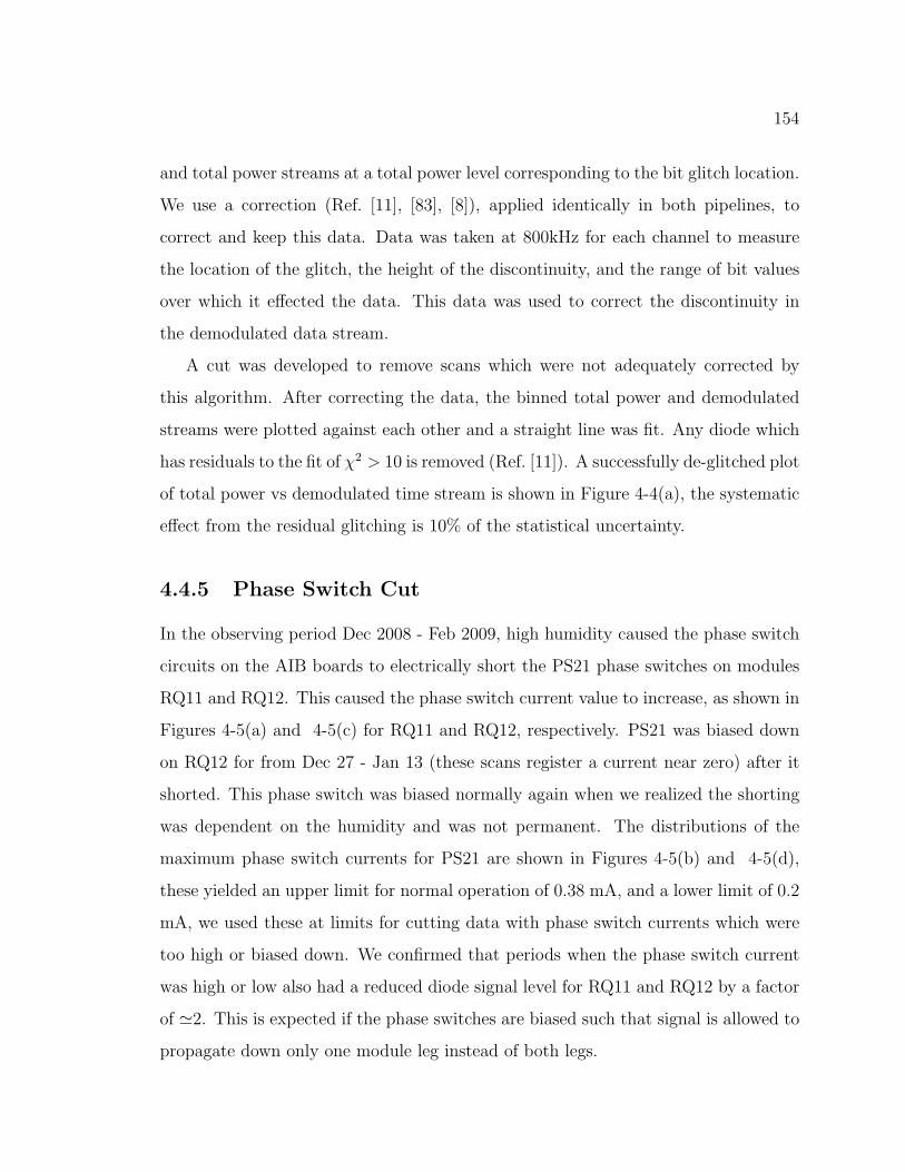
154
and total power streams at a total power level corresponding to the bit glitch location.
We use a correction (Ref. [11], [83], [8]), applied identically in both pipelines, to
correct and keep this data. Data was taken at 800kHz for each channel to measure
the location of the glitch, the height of the discontinuity, and the range of bit values
over which it effected the data. This data was used to correct the discontinuity in
the demodulated data stream.
A cut was developed to remove scans which were not adequately corrected by
this algorithm. After correcting the data, the binned total power and demodulated
streams were plotted against each other and a straight line was fit. Any diode which
has residuals to the fit of χ2
> 10 is removed (Ref. [11]). A successfully de-glitched plot
of total power vs demodulated time stream is shown in Figure 4-4(a), the systematic
effect from the residual glitching is 10% of the statistical uncertainty.
4.4.5 Phase Switch Cut
In the observing period Dec 2008 - Feb 2009, high humidity caused the phase switch
circuits on the AIB boards to electrically short the PS21 phase switches on modules
RQ11 and RQ12. This caused the phase switch current value to increase, as shown in
Figures 4-5(a) and 4-5(c) for RQ11 and RQ12, respectively. PS21 was biased down
on RQ12 for from Dec 27 - Jan 13 (these scans register a current near zero) after it
shorted. This phase switch was biased normally again when we realized the shorting
was dependent on the humidity and was not permanent. The distributions of the
maximum phase switch currents for PS21 are shown in Figures 4-5(b) and 4-5(d),
these yielded an upper limit for normal operation of 0.38 mA, and a lower limit of 0.2
mA, we used these at limits for cutting data with phase switch currents which were
too high or biased down. We confirmed that periods when the phase switch current
was high or low also had a reduced diode signal level for RQ11 and RQ12 by a factor
of 2. This is expected if the phase switches are biased such that signal is allowed to
propagate down only one module leg instead of both legs.
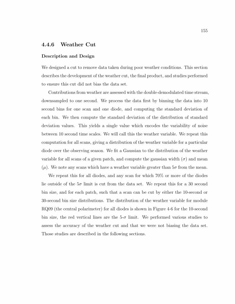
155
4.4.6 Weather Cut
Description and Design
We designed a cut to remove data taken during poor weather conditions. This section
describes the development of the weather cut, the final product, and studies performed
to ensure this cut did not bias the data set.
Contributions from weather are assessed with the double-demodulated time stream,
downsampled to one second. We process the data first by binning the data into 10
second bins for one scan and one diode, and computing the standard deviation of
each bin. We then compute the standard deviation of the distribution of standard
deviation values. This yields a single value which encodes the variability of noise
between 10 second time scales. We will call this the weather variable. We repeat this
computation for all scans, giving a distribution of the weather variable for a particular
diode over the observing season. We fit a Gaussian to the distribution of the weather
variable for all scans of a given patch, and compute the gaussian width (σ) and mean
(µ). We note any scans which have a weather variable greater than 5σ from the mean.
We repeat this for all diodes, and any scan for which 70% or more of the diodes
lie outside of the 5σ limit is cut from the data set. We repeat this for a 30 second
bin size, and for each patch, such that a scan can be cut by either the 10-second or
30-second bin size distributions. The distribution of the weather variable for module
RQ09 (the central polarimeter) for all diodes is shown in Figure 4-6 for the 10-second
bin size, the red vertical lines are the 5-σ limit. We performed various studies to
assess the accuracy of the weather cut and that we were not biasing the data set.
Those studies are described in the following sections.
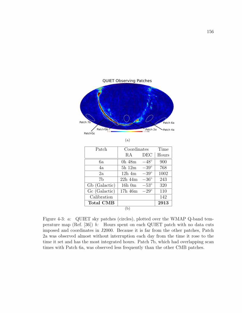
156
(a)
Patch Coordinates TimeRA DEC Hours
6a 0h 48m −48 9004a 5h 12m −39 7682a 12h 4m −39 10027b 22h 44m −36 243
Gb (Galactic) 16h 0m −53 320Gc (Galactic) 17h 46m −29 110Calibration 142
Total CMB 2913(b)
Figure 4-3: a: QUIET sky patches (circles), plotted over the WMAP Q-band tem-perature map (Ref. [36]) b: Hours spent on each QUIET patch with no data cutsimposed and coordinates in J2000. Because it is far from the other patches, Patch2a was observed almost without interruption each day from the time it rose to thetime it set and has the most integrated hours. Patch 7b, which had overlapping scantimes with Patch 6a, was observed less frequently than the other CMB patches.
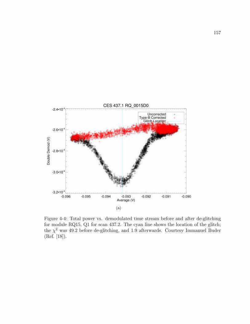
157
(a)
Figure 4-4: Total power vs. demodulated time stream before and after de-glitchingfor module RQ15, Q1 for scan 437.2. The cyan line shows the location of the glitch;the χ
2 was 49.2 before de-glitching, and 1.9 afterwards. Courtesy Immanuel Buder(Ref. [18]).
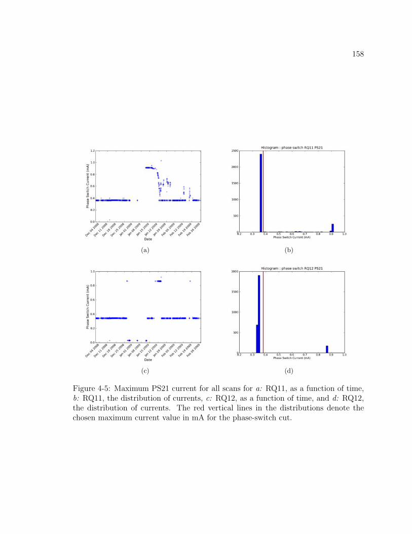
158
(a) (b)
(c) (d)
Figure 4-5: Maximum PS21 current for all scans for a: RQ11, as a function of time,b: RQ11, the distribution of currents, c: RQ12, as a function of time, and d: RQ12,the distribution of currents. The red vertical lines in the distributions denote thechosen maximum current value in mA for the phase-switch cut.
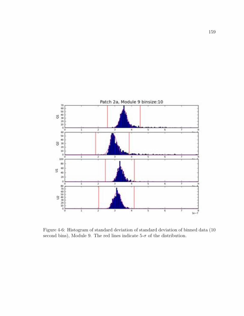
159
Figure 4-6: Histogram of standard deviation of standard deviation of binned data (10second bins), Module 9. The red lines indicate 5-σ of the distribution.
160
Studies
Time Scales for Weather Variable
The temperature of the enclosure drifts on a variety of time scales, and with it, the
polarimeter data stream. This effect can be corrected in further analysis steps, and
so we must choose a weather variable which selects only periods of bad weather, and
does not flag data which is varying only from the enclosure temperature. The two
effects are illustrated in Figures 4-7(a) and 4-7(b); these show the time-streams for
scan 404, which has a clear spike originating from a cloud, and scan 1776, which has
a signal envelope dependent only on the enclosure temperature and is not an example
of bad weather.
To isolate and cut scans which are affected by bad weather, we investigated a
variety of binning time scales: 5 seconds, 10 seconds, 30 seconds, 60 seconds, and
120 seconds. The standard deviation of each bin for these bin sizes is shown for scan
404 (Figure 4-8(a)) and scan 1776 (Figure 4-8(b)). The significance of the weather
variable for each of these bin sizes for both scans is given in Table 4.2. The spike from
weather in scan 404 was detected at all bin sizes. Enclosure temperature variation was
apparent by a bin size of 60 seconds as it includes the rise of the enclosure temperature
in the RMS statistic. The 30 second bin size generally had the highest significance for
weather. We included the 10 second time bin because it is near the scan frequency,
and so will have sensitivity to stationary weather patterns. The overlap between the
two bin-size cuts is 80%, and is dominated by the Q-diodes (which have higher
leakage and make up a larger percentage of the weather cut). A visual inspection of
all scans which were cut by only one showed that both cuts were removing bad data,
so both cuts were retained.
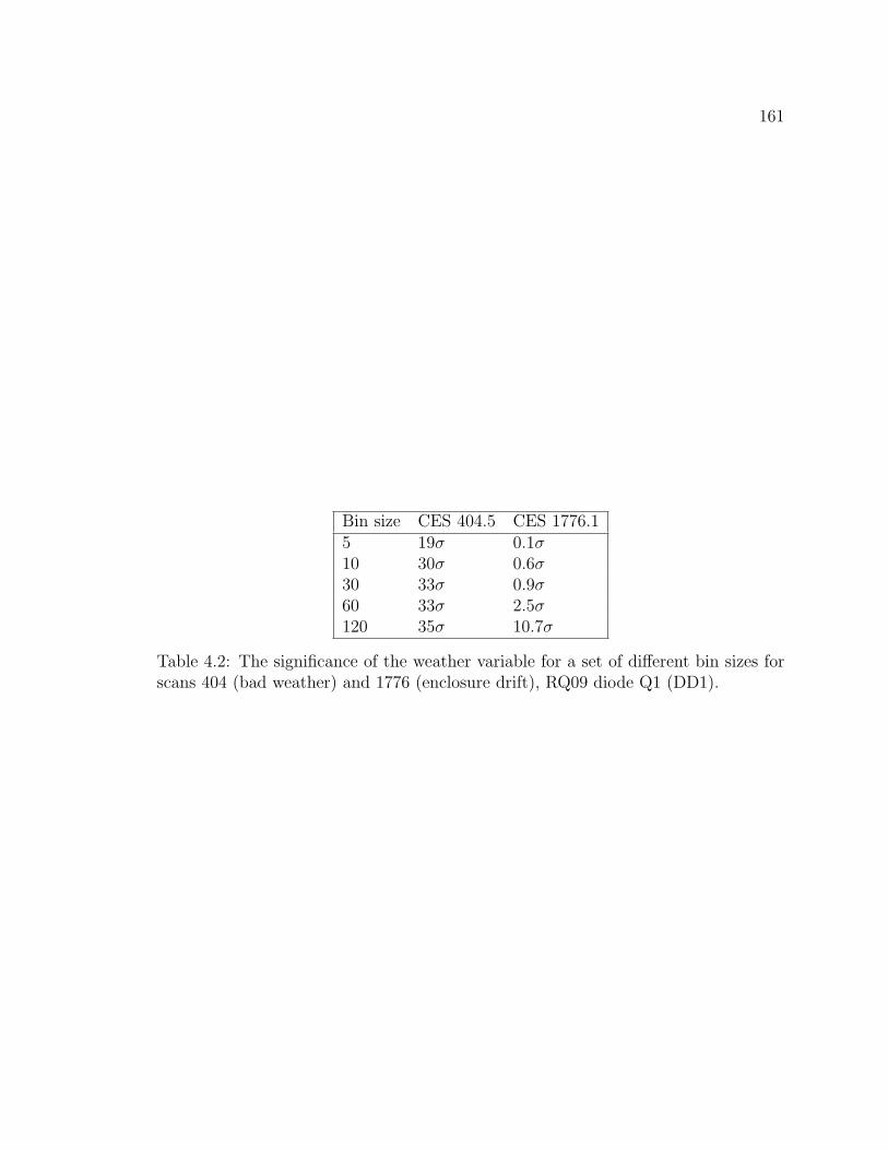
161
Bin size CES 404.5 CES 1776.15 19σ 0.1σ10 30σ 0.6σ30 33σ 0.9σ60 33σ 2.5σ120 35σ 10.7σ
Table 4.2: The significance of the weather variable for a set of different bin sizes forscans 404 (bad weather) and 1776 (enclosure drift), RQ09 diode Q1 (DD1).
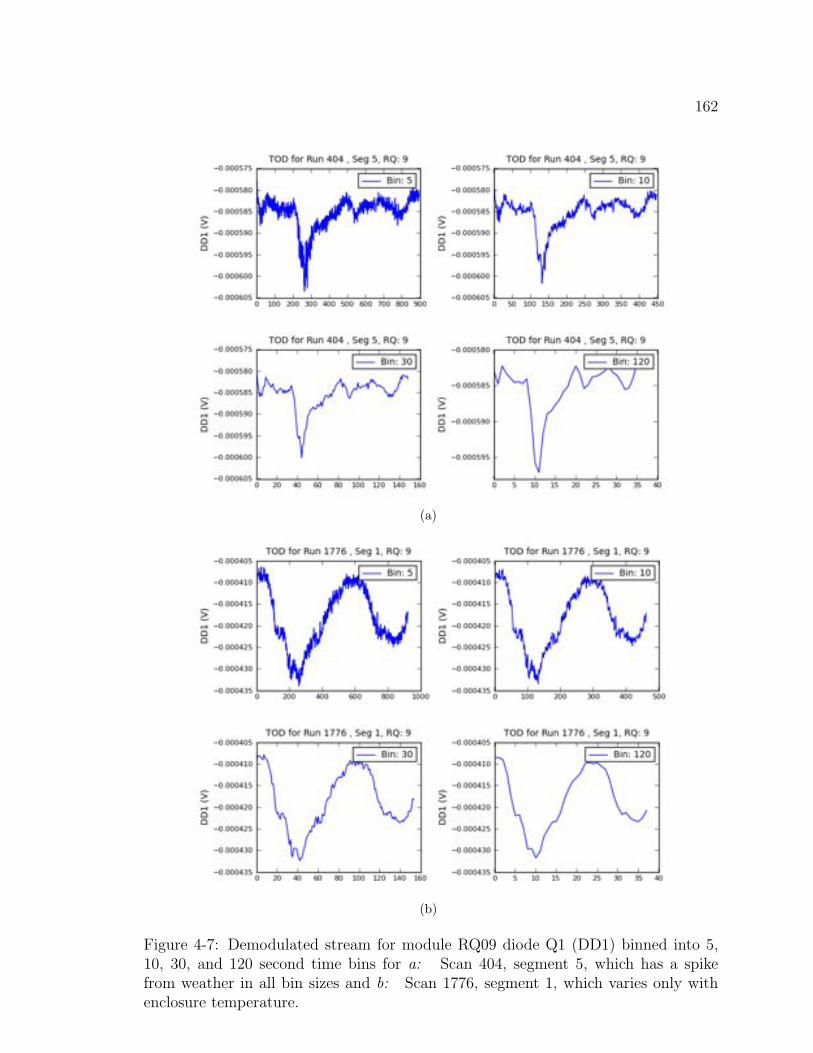
162
(a)
(b)
Figure 4-7: Demodulated stream for module RQ09 diode Q1 (DD1) binned into 5,10, 30, and 120 second time bins for a: Scan 404, segment 5, which has a spikefrom weather in all bin sizes and b: Scan 1776, segment 1, which varies only withenclosure temperature.
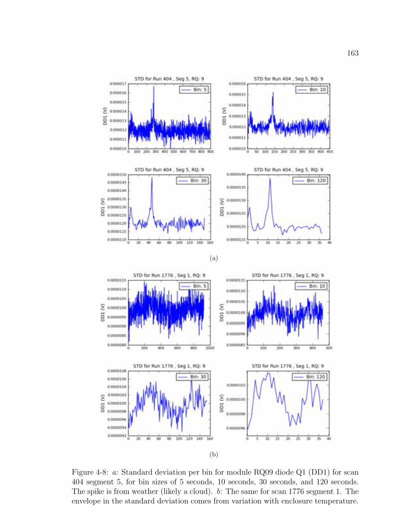
163
(a)
(b)
Figure 4-8: a: Standard deviation per bin for module RQ09 diode Q1 (DD1) for scan404 segment 5, for bin sizes of 5 seconds, 10 seconds, 30 seconds, and 120 seconds.The spike is from weather (likely a cloud). b: The same for scan 1776 segment 1. Theenvelope in the standard deviation comes from variation with enclosure temperature.
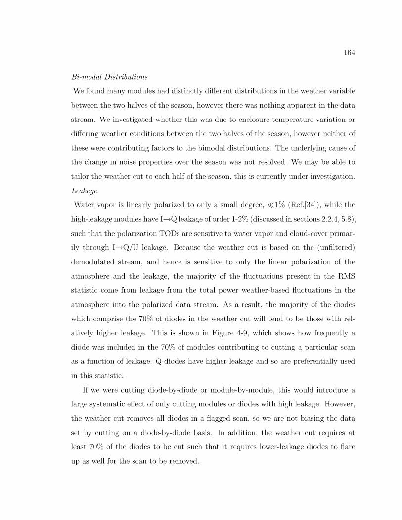
164
Bi-modal Distributions
We found many modules had distinctly different distributions in the weather variable
between the two halves of the season, however there was nothing apparent in the data
stream. We investigated whether this was due to enclosure temperature variation or
differing weather conditions between the two halves of the season, however neither of
these were contributing factors to the bimodal distributions. The underlying cause of
the change in noise properties over the season was not resolved. We may be able to
tailor the weather cut to each half of the season, this is currently under investigation.
Leakage
Water vapor is linearly polarized to only a small degree, 1% (Ref.[34]), while the
high-leakage modules have I→Q leakage of order 1-2% (discussed in sections 2.2.4, 5.8),
such that the polarization TODs are sensitive to water vapor and cloud-cover primar-
ily through I→Q/U leakage. Because the weather cut is based on the (unfiltered)
demodulated stream, and hence is sensitive to only the linear polarization of the
atmosphere and the leakage, the majority of the fluctuations present in the RMS
statistic come from leakage from the total power weather-based fluctuations in the
atmosphere into the polarized data stream. As a result, the majority of the diodes
which comprise the 70% of diodes in the weather cut will tend to be those with rel-
atively higher leakage. This is shown in Figure 4-9, which shows how frequently a
diode was included in the 70% of modules contributing to cutting a particular scan
as a function of leakage. Q-diodes have higher leakage and so are preferentially used
in this statistic.
If we were cutting diode-by-diode or module-by-module, this would introduce a
large systematic effect of only cutting modules or diodes with high leakage. However,
the weather cut removes all diodes in a flagged scan, so we are not biasing the data
set by cutting on a diode-by-diode basis. In addition, the weather cut requires at
least 70% of the diodes to be cut such that it requires lower-leakage diodes to flare
up as well for the scan to be removed.
165
Figure 4-9: The weather cut requires that 70% of the diodes lie outside of a 5-σthreshold, this shows which diodes make up that 70% as a function of leakage. It isapparent that higher-leakage modules appear more frequently in the list of modulescut. Because weather effects both the demodulated and total power streams, andleakage is contamination from total power into the demodulated stream, this isn’tunexpected. This study was done with patch 2a data only.
Bias
We created a set of simulated time-ordered-data with noise only (no signal) using
the same simulation code we use in the Maximum-likelihood analysis pipeline for
power spectrum analysis (section 6.4.3). The simulation code uses the pointing and
calibration information for a set of selected scans (in our case 44, ideally we would
draw a larger sample size but we have been limited by computation time), and uses
the noise model (described below in section 4.4.7) and an input power spectrum to
generate a set of TODs. In our case, the signal spectrum is null, allowing us to test
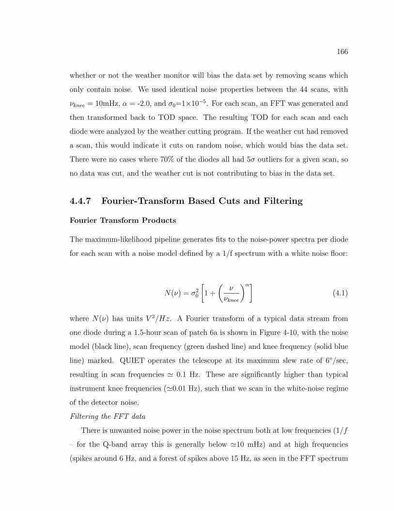
166
whether or not the weather monitor will bias the data set by removing scans which
only contain noise. We used identical noise properties between the 44 scans, with
νknee = 10mHz, α = -2.0, and σ0=1×10⁻⁵. For each scan, an FFT was generated and
then transformed back to TOD space. The resulting TOD for each scan and each
diode were analyzed by the weather cutting program. If the weather cut had removed
a scan, this would indicate it cuts on random noise, which would bias the data set.
There were no cases where 70% of the diodes all had 5σ outliers for a given scan, so
no data was cut, and the weather cut is not contributing to bias in the data set.
4.4.7 Fourier-Transform Based Cuts and Filtering
Fourier Transform Products
The maximum-likelihood pipeline generates fits to the noise-power spectra per diode
for each scan with a noise model defined by a 1/f spectrum with a white noise floor:
N(ν) = σ2
0
1 +
ν
νknee
α(4.1)
where N(ν) has units V2/Hz. A Fourier transform of a typical data stream from
one diode during a 1.5-hour scan of patch 6a is shown in Figure 4-10, with the noise
model (black line), scan frequency (green dashed line) and knee frequency (solid blue
line) marked. QUIET operates the telescope at its maximum slew rate of 6/sec,
resulting in scan frequencies 0.1 Hz. These are significantly higher than typical
instrument knee frequencies (0.01 Hz), such that we scan in the white-noise regime
of the detector noise.
Filtering the FFT data
There is unwanted noise power in the noise spectrum both at low frequencies (1/f
– for the Q-band array this is generally below 10 mHz) and at high frequencies
(spikes around 6 Hz, and a forest of spikes above 15 Hz, as seen in the FFT spectrum
167
in Figure 4-10). The origin of the high frequency noise spikes is unclear, likely they
are harmonics and noise aliasing of the power-line frequency (50Hz and 60Hz) and
the switching and timing frequencies in the electronics system. To remove this noise,
we filter the spectrum using:
F (ν) =1
1 + ( ννapod
)αapod(4.2)
with two separate sets of filter parameters: the low-pass filter has νapod=4.5.Hz and
αapod = 200; the high-pass filter has νapod = 2.5νscan and αapod = −40. The CMB
signal is periodic in the Fourier domain at harmonics of the scan frequency, so the
total integrated power in the first few harmonics is negligible compared to the power
in the higher harmonics. Thus, filtering at low frequencies removes mostly noise
and hardly any signal and so we chose the νapod for the high-pass filter to cut out
noise below 2.5× the scan frequency. The resolution of the beam begins to affect the
signal-to-noise at higher harmonics thus we can filter high-frequency noise without
incurring much data loss. A low-pass filter cut-off of 4.5 Hz removes 25% of the
signal (Ref. [8]), we are currently investigating whether we can move the filter and
retain more data. There are two reasons to filter this data: one is that there are spikes
at high-frequencies which trigger a data cut. The second is that in the frequency
range where the beam begins to roll off, the signal level is decreasing but the noise
stays constant, decreasing your signal-to-noise. The noise spectrum before and after
filtering is shown in Figure 4-10, it is apparent that both the high-frequency spiking
and the low-frequency 1/f noise has been filtered out.
Data cutting with FFT data
We compute the χ2 between the FFT of the data and noise model fit-line for each
diode for each scan in the ranges: 0 - 2.5νscan mHz, 2.5νscan - 7Hz; we use only the
range 200 mHz - 7 Hz for data cutting. The FFT χ2 is defined as
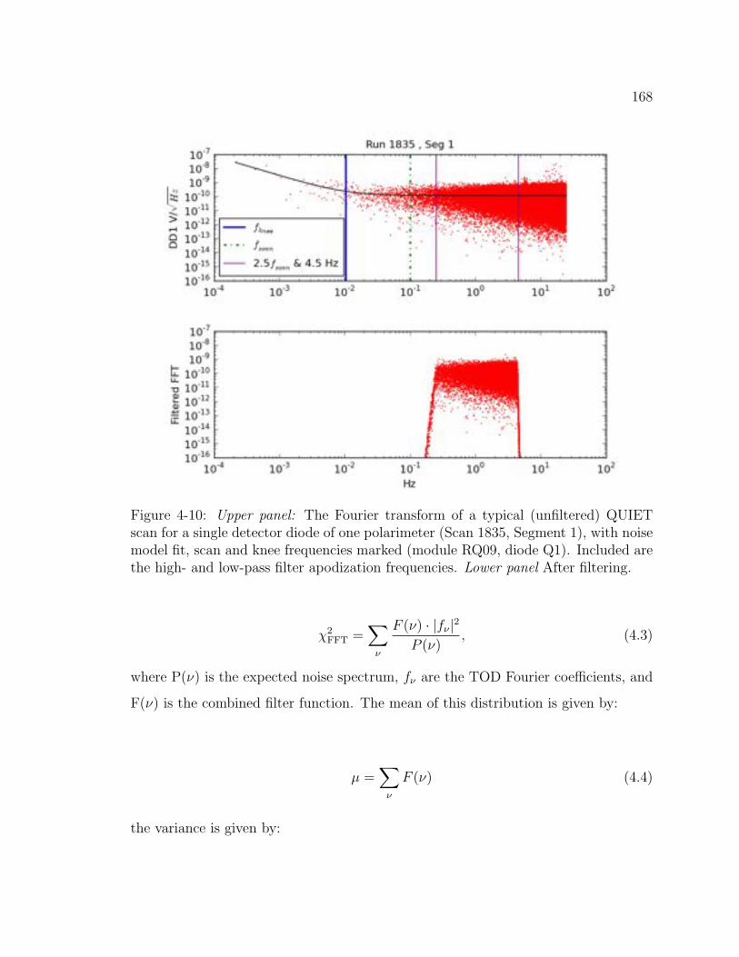
168
Figure 4-10: Upper panel: The Fourier transform of a typical (unfiltered) QUIETscan for a single detector diode of one polarimeter (Scan 1835, Segment 1), with noisemodel fit, scan and knee frequencies marked (module RQ09, diode Q1). Included arethe high- and low-pass filter apodization frequencies. Lower panel After filtering.
χ2
FFT=
ν
F (ν) · |fν |2
P (ν), (4.3)
where P(ν) is the expected noise spectrum, fν are the TOD Fourier coefficients, and
F(ν) is the combined filter function. The mean of this distribution is given by:
µ =
ν
F (ν) (4.4)
the variance is given by:
169
σ2 =
ν
F (ν)2 (4.5)
and the agreement between the fit and the data is quantified by
Nσ =χ
2 − µ
σ(4.6)
The distribution of Nσ values for all scans and all diodes for the range 2.5νscan-7Hz
is shown in Figure 4-11, and compared to the distribution obtained from simulated
data streams (noise only). If the average Nσ is greater than 4-σ between 2.5νscan -
7Hz, the diode is cut for that CES segment. We also cut a diode from a scan if the
diode knee frequency its higher than 50mHz. We are investigating whether we can
shift this cutoff frequency higher given the high-pass filtering frequency of 200mHz.
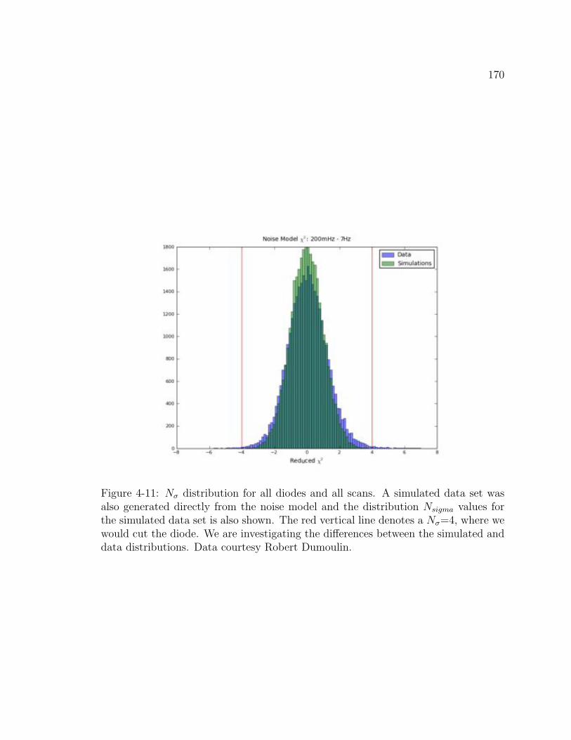
170
Figure 4-11: Nσ distribution for all diodes and all scans. A simulated data set wasalso generated directly from the noise model and the distribution Nsigma values forthe simulated data set is also shown. The red vertical line denotes a Nσ=4, where wewould cut the diode. We are investigating the differences between the simulated anddata distributions. Data courtesy Robert Dumoulin.
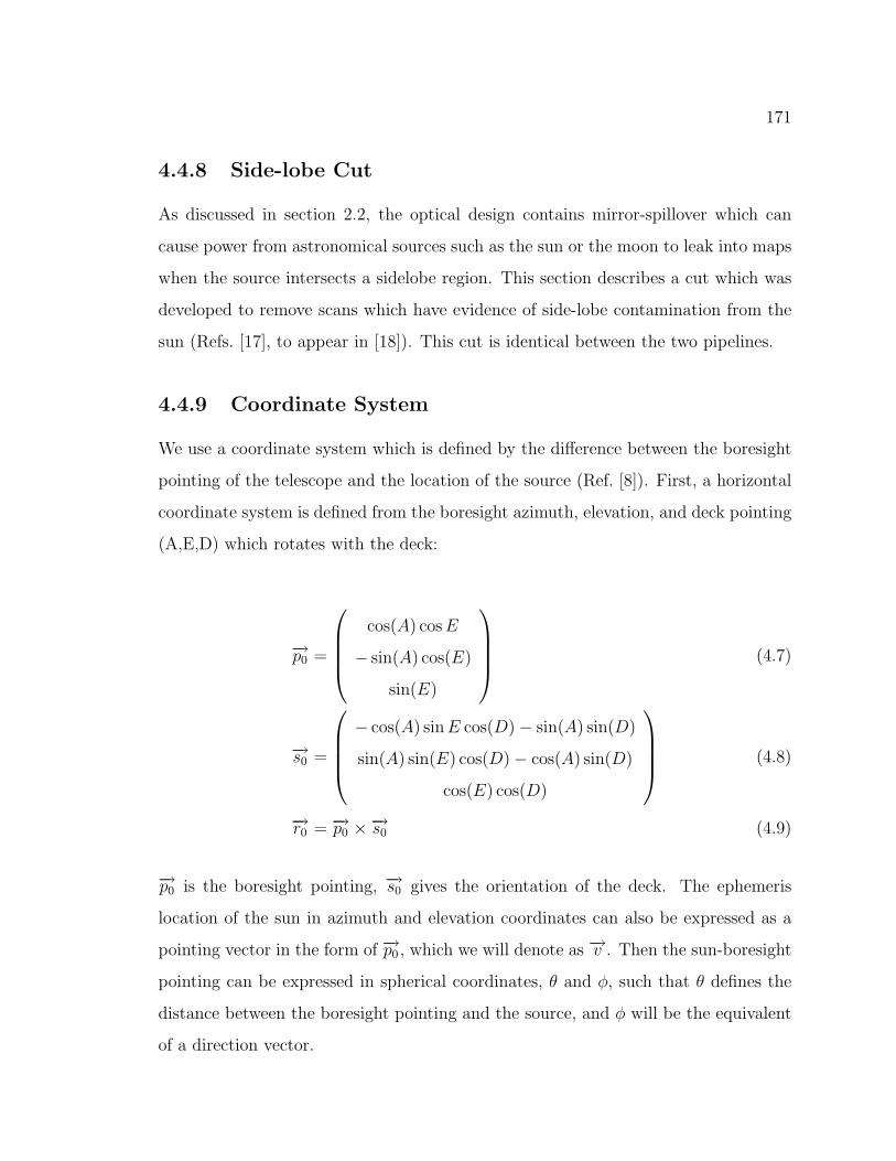
171
4.4.8 Side-lobe Cut
As discussed in section 2.2, the optical design contains mirror-spillover which can
cause power from astronomical sources such as the sun or the moon to leak into maps
when the source intersects a sidelobe region. This section describes a cut which was
developed to remove scans which have evidence of side-lobe contamination from the
sun (Refs. [17], to appear in [18]). This cut is identical between the two pipelines.
4.4.9 Coordinate System
We use a coordinate system which is defined by the difference between the boresight
pointing of the telescope and the location of the source (Ref. [8]). First, a horizontal
coordinate system is defined from the boresight azimuth, elevation, and deck pointing
(A,E,D) which rotates with the deck:
−→p0 =
cos(A) cos E
− sin(A) cos(E)
sin(E)
(4.7)
−→s0 =
− cos(A) sin E cos(D)− sin(A) sin(D)
sin(A) sin(E) cos(D)− cos(A) sin(D)
cos(E) cos(D)
(4.8)
−→r0 = −→
p0 ×−→s0 (4.9)
−→p0 is the boresight pointing, −→s0 gives the orientation of the deck. The ephemeris
location of the sun in azimuth and elevation coordinates can also be expressed as a
pointing vector in the form of −→p0 , which we will denote as −→v . Then the sun-boresight
pointing can be expressed in spherical coordinates, θ and φ, such that θ defines the
distance between the boresight pointing and the source, and φ will be the equivalent
of a direction vector.
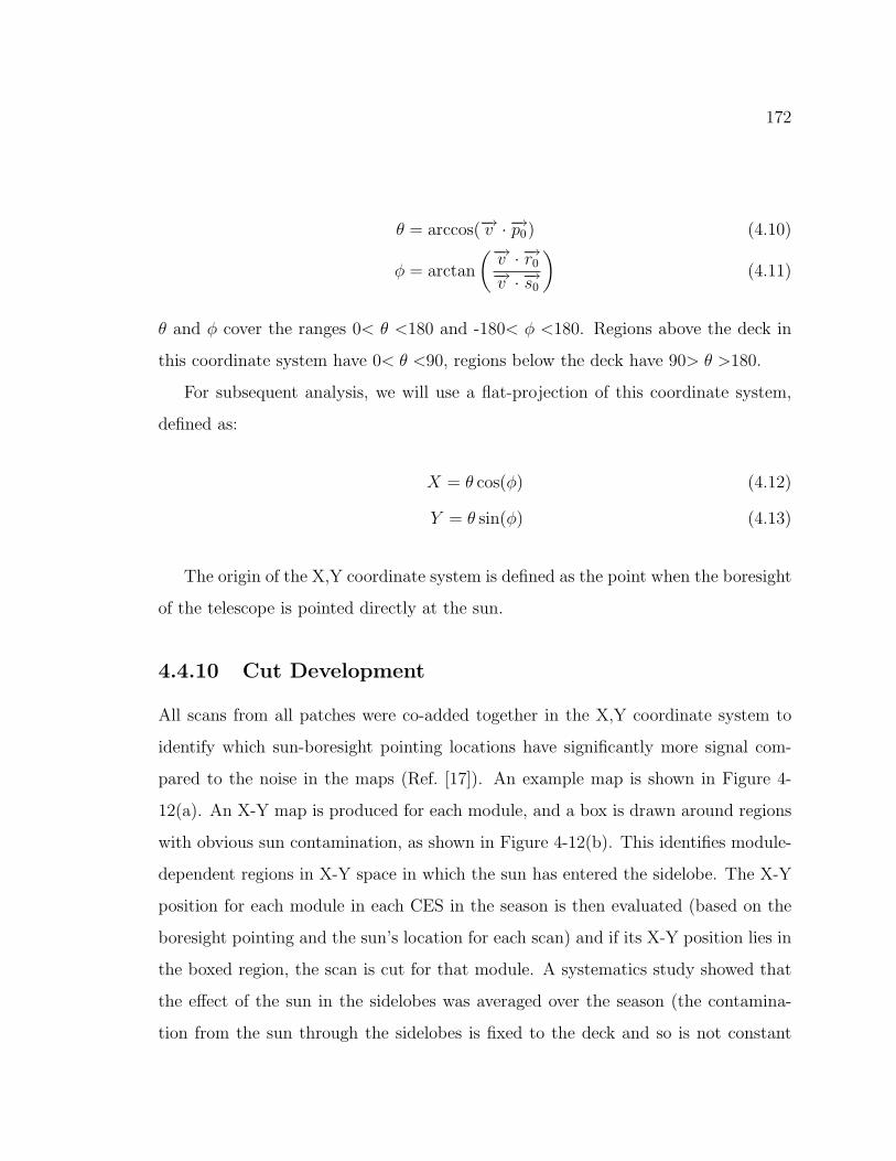
172
θ = arccos(−→v ·−→p0) (4.10)
φ = arctan
−→v ·−→r0
−→v ·−→s0
(4.11)
θ and φ cover the ranges 0< θ <180 and -180< φ <180. Regions above the deck in
this coordinate system have 0< θ <90, regions below the deck have 90> θ >180.
For subsequent analysis, we will use a flat-projection of this coordinate system,
defined as:
X = θ cos(φ) (4.12)
Y = θ sin(φ) (4.13)
The origin of the X,Y coordinate system is defined as the point when the boresight
of the telescope is pointed directly at the sun.
4.4.10 Cut Development
All scans from all patches were co-added together in the X,Y coordinate system to
identify which sun-boresight pointing locations have significantly more signal com-
pared to the noise in the maps (Ref. [17]). An example map is shown in Figure 4-
12(a). An X-Y map is produced for each module, and a box is drawn around regions
with obvious sun contamination, as shown in Figure 4-12(b). This identifies module-
dependent regions in X-Y space in which the sun has entered the sidelobe. The X-Y
position for each module in each CES in the season is then evaluated (based on the
boresight pointing and the sun’s location for each scan) and if its X-Y position lies in
the boxed region, the scan is cut for that module. A systematics study showed that
the effect of the sun in the sidelobes was averaged over the season (the contamina-
tion from the sun through the sidelobes is fixed to the deck and so is not constant
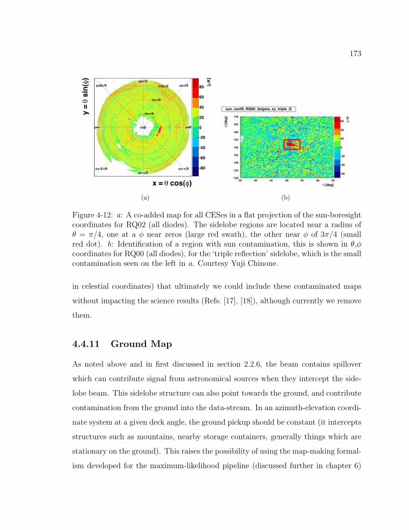
173
(a) (b)
Figure 4-12: a: A co-added map for all CESes in a flat projection of the sun-boresightcoordinates for RQ02 (all diodes). The sidelobe regions are located near a radius ofθ = π/4, one at a φ near zeros (large red swath), the other near φ of 3π/4 (smallred dot). b: Identification of a region with sun contamination, this is shown in θ,φcoordinates for RQ00 (all diodes), for the ‘triple reflection’ sidelobe, which is the smallcontamination seen on the left in a. Courtesy Yuji Chinone.
in celestial coordinates) that ultimately we could include these contaminated maps
without impacting the science results (Refs. [17], [18]), although currently we remove
them.
4.4.11 Ground Map
As noted above and in first discussed in section 2.2.6, the beam contains spillover
which can contribute signal from astronomical sources when they intercept the side-
lobe beam. This sidelobe structure can also point towards the ground, and contribute
contamination from the ground into the data-stream. In an azimuth-elevation coordi-
nate system at a given deck angle, the ground pickup should be constant (it intercepts
structures such as mountains, nearby storage containers, generally things which are
stationary on the ground). This raises the possibility of using the map-making formal-
ism developed for the maximum-likelihood pipeline (discussed further in chapter 6)
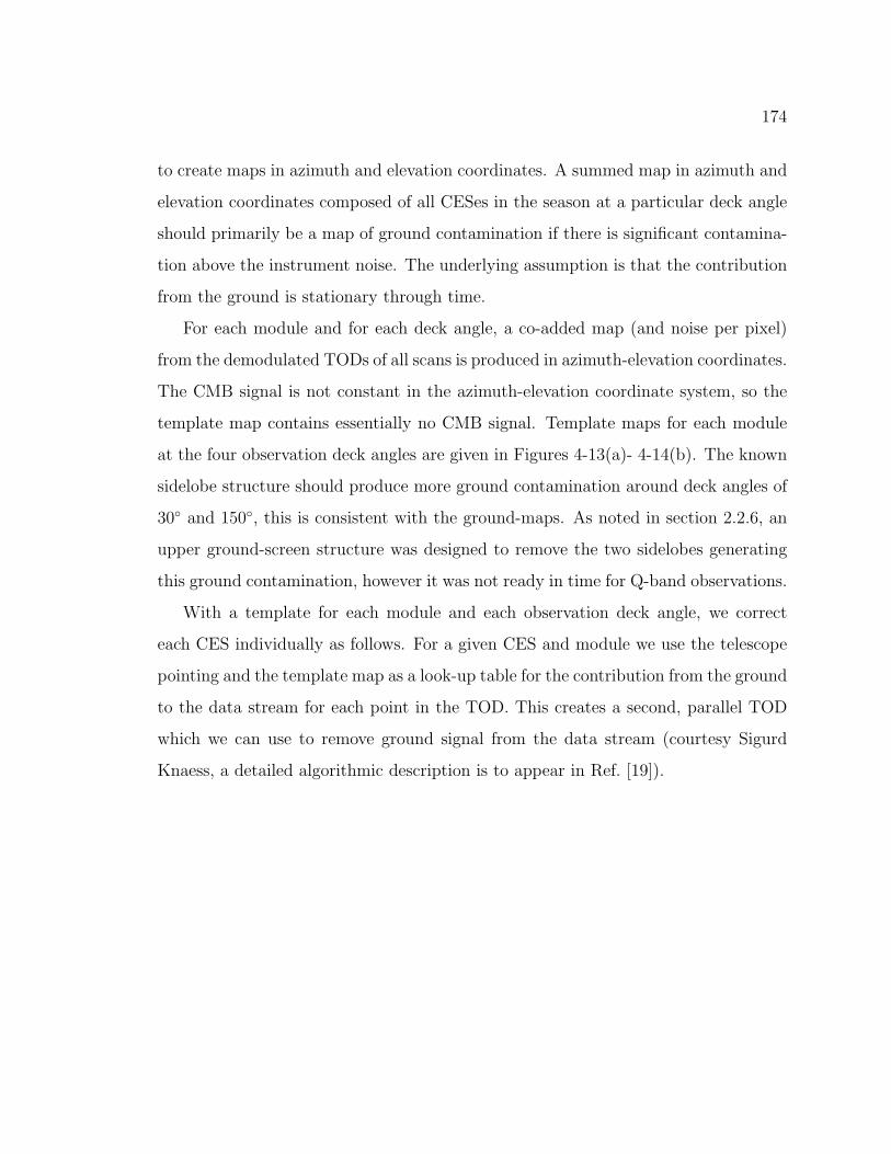
174
to create maps in azimuth and elevation coordinates. A summed map in azimuth and
elevation coordinates composed of all CESes in the season at a particular deck angle
should primarily be a map of ground contamination if there is significant contamina-
tion above the instrument noise. The underlying assumption is that the contribution
from the ground is stationary through time.
For each module and for each deck angle, a co-added map (and noise per pixel)
from the demodulated TODs of all scans is produced in azimuth-elevation coordinates.
The CMB signal is not constant in the azimuth-elevation coordinate system, so the
template map contains essentially no CMB signal. Template maps for each module
at the four observation deck angles are given in Figures 4-13(a)- 4-14(b). The known
sidelobe structure should produce more ground contamination around deck angles of
30 and 150, this is consistent with the ground-maps. As noted in section 2.2.6, an
upper ground-screen structure was designed to remove the two sidelobes generating
this ground contamination, however it was not ready in time for Q-band observations.
With a template for each module and each observation deck angle, we correct
each CES individually as follows. For a given CES and module we use the telescope
pointing and the template map as a look-up table for the contribution from the ground
to the data stream for each point in the TOD. This creates a second, parallel TOD
which we can use to remove ground signal from the data stream (courtesy Sigurd
Knaess, a detailed algorithmic description is to appear in Ref. [19]).
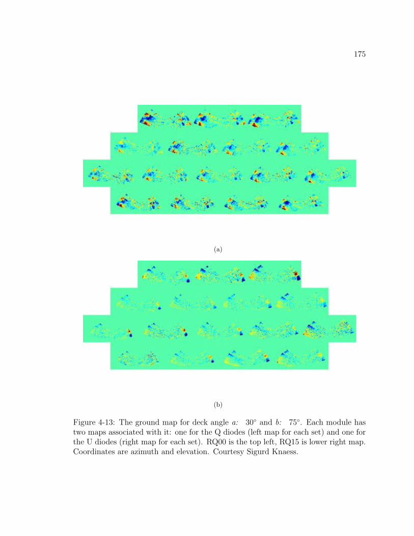
175
(a)
(b)
Figure 4-13: The ground map for deck angle a: 30 and b: 75. Each module hastwo maps associated with it: one for the Q diodes (left map for each set) and one forthe U diodes (right map for each set). RQ00 is the top left, RQ15 is lower right map.Coordinates are azimuth and elevation. Courtesy Sigurd Knaess.
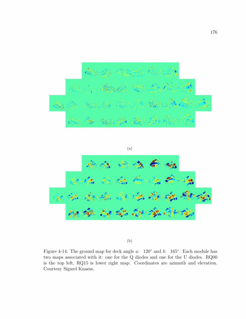
176
(a)
(b)
Figure 4-14: The ground map for deck angle a: 120 and b: 165. Each module hastwo maps associated with it: one for the Q diodes and one for the U diodes. RQ00is the top left, RQ15 is lower right map. Coordinates are azimuth and elevation.Courtesy Sigurd Knaess.
177
Figure 4-15: Spike in the demodulated stream for scan 1219, segment 3 for moduleRQ00. This was rejected with an outlier statistic of 41, 33, 30, 41 σ, for the Q1, U1,U2, and Q2 diodes respectively.
4.4.12 Max-Min Removal
We compute an outlier statistic to identify spikes in the time-ordered data stream.
For each CES and each diode, the average and the root-mean-square of the data
stream for the CES TOD is computed. The deviation from the mean is computed
for each point in the TOD, and divided by the RMS to obtain an outlier statistic
(equation 4.14, [19]). If the absolute value of the maximum outlier is greater than
7.0, the CES is removed from the scan for that diode. A TOD from one scan and
module removed by this statistic is shown in Figure 4-15.
Outlier = |MAX(X −X
XRMS)| (4.14)
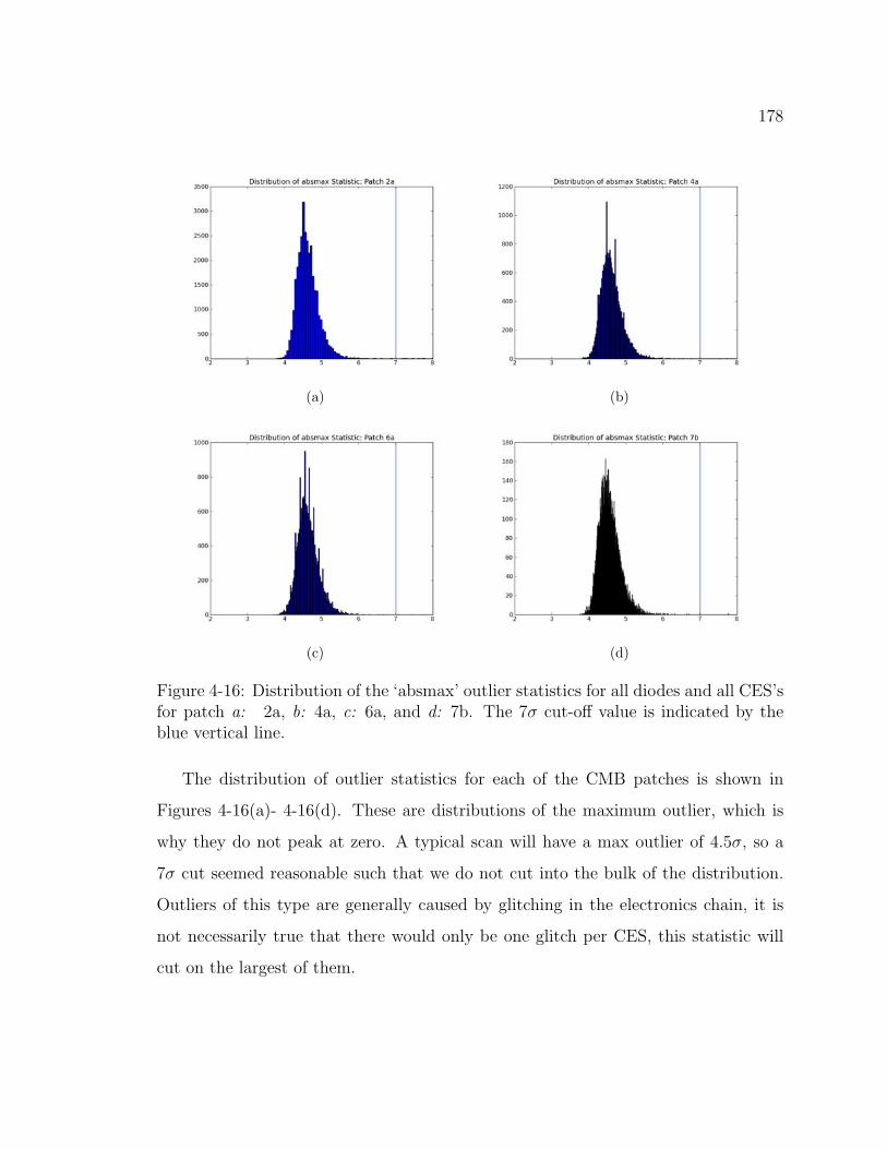
178
(a) (b)
(c) (d)
Figure 4-16: Distribution of the ‘absmax’ outlier statistics for all diodes and all CES’sfor patch a: 2a, b: 4a, c: 6a, and d: 7b. The 7σ cut-off value is indicated by theblue vertical line.
The distribution of outlier statistics for each of the CMB patches is shown in
Figures 4-16(a)- 4-16(d). These are distributions of the maximum outlier, which is
why they do not peak at zero. A typical scan will have a max outlier of 4.5σ, so a
7σ cut seemed reasonable such that we do not cut into the bulk of the distribution.
Outliers of this type are generally caused by glitching in the electronics chain, it is
not necessarily true that there would only be one glitch per CES, this statistic will
cut on the largest of them.
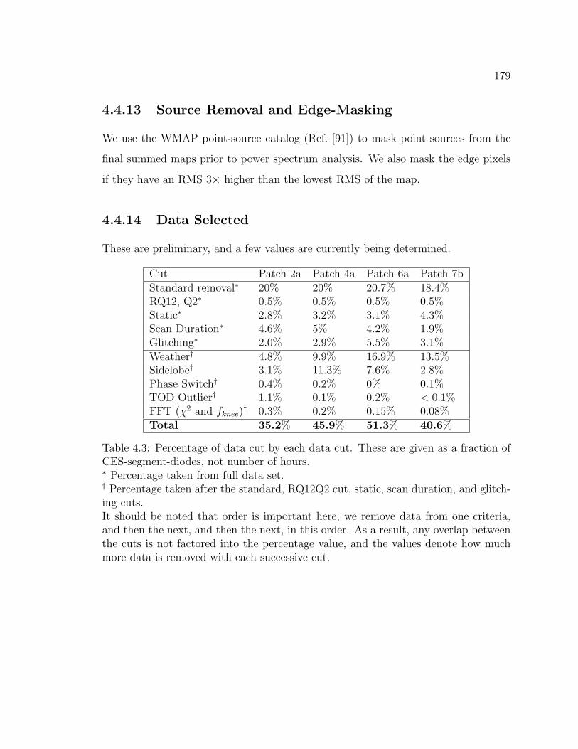
179
4.4.13 Source Removal and Edge-Masking
We use the WMAP point-source catalog (Ref. [91]) to mask point sources from the
final summed maps prior to power spectrum analysis. We also mask the edge pixels
if they have an RMS 3× higher than the lowest RMS of the map.
4.4.14 Data Selected
These are preliminary, and a few values are currently being determined.
Cut Patch 2a Patch 4a Patch 6a Patch 7bStandard removal∗ 20% 20% 20.7% 18.4%RQ12, Q2∗ 0.5% 0.5% 0.5% 0.5%Static∗ 2.8% 3.2% 3.1% 4.3%Scan Duration∗ 4.6% 5% 4.2% 1.9%Glitching∗ 2.0% 2.9% 5.5% 3.1%Weather† 4.8% 9.9% 16.9% 13.5%Sidelobe† 3.1% 11.3% 7.6% 2.8%Phase Switch† 0.4% 0.2% 0% 0.1%TOD Outlier† 1.1% 0.1% 0.2% < 0.1%FFT (χ2 and fknee)† 0.3% 0.2% 0.15% 0.08%Total 35.2% 45.9% 51.3% 40.6%
Table 4.3: Percentage of data cut by each data cut. These are given as a fraction ofCES-segment-diodes, not number of hours.∗ Percentage taken from full data set.† Percentage taken after the standard, RQ12Q2 cut, static, scan duration, and glitch-ing cuts.It should be noted that order is important here, we remove data from one criteria,and then the next, and then the next, in this order. As a result, any overlap betweenthe cuts is not factored into the percentage value, and the values denote how muchmore data is removed with each successive cut.
Chapter 5
Instrument Calibration and
Characterization
5.1 Introduction
We dedicate 10% of the QUIET observing season to instrument calibration ob-
servations. This chapter summarizes calibration procedures, products, uncertain-
ties, and the resulting systematic errors from measurements of pointing, responsivity,
polarimeter angle definitions, leakage, receiver bandpasses, beams, and correlated
noise. QUIET has two independent data analysis pipelines (Maximum Likelihood
and Pseudo-C), I will describe the calibration for the Maximum Likelihood pipeline
but they are similar. Instrument calibration analysis was performed by many collab-
orators, this is meant as a summary with final results to appear in Ref. [18].
5.1.1 Nomenclature
• Polarization modules - the 16 modules which are attached to the OMTs, these
modules will measure the Q and U Stokes parameters in the differenced stream.
• hybrid-Tee modules - the two modules attached to the hybrid-Tee assembly,
180
181
these measure differential temperature between their two feedhorns.
• Drift Scan - A repetitive azimuth scan that uses the sky rotation to allow the
source to drift through the beam. These allow us to scan through a constant
column density of atmosphere.
• Raster Scan - A scan performed in which an we slew in azimuth twice and
re-track the source, generally changing the elevation of the telescope. Raster
scans of calibration sources will typically need additional processing to remove
the effects of changing atmospheric depth during the course of the scan.
• Constant Elevation Scan (CES) - this was described in Chapter 4.
5.2 Calibration Overview
5.2.1 Calibration Sources
Calibration sources are described below and the Q-band calibration scheme is sum-
marized in Table 5.1.
• Tau A, or the Crab Nebula, is a supernova remnant with a polarized flux at Q-
band known to an accuracy of ±2.7% from WMAP measurements (Ref. [90]).
We perform measurements of Tau A with the central polarimeter every two
nights, and with all other polarimeters at least once during the observing season.
The maximum angle that Tau A rises above the horizon is usually within 5
of the lower elevation limit of the telescope, which is too low to use a drift
scan for the central polarimeter. Instead, we employ a raster scan, observing
at four deck angles 30,75,120,165 such that we can use these measurements
for polarization angle calibration. The polarized brightness of Tau A is 22.1 Jy
(Ref [90]).
182
• The Moon We employ either a drift scan or a raster scan to observe the moon
with each polarimeter during a single moon calibration measurement; this is
performed once each week. A model of the moon (Ref. [8]) gives an expected
polarization of 1K. We use a raster scan when the moon does not rise to a
high enough elevation to drift through the entire beam.
• Mini Sky-dips We perform ”mini sky-dips” once for each constant elevation
scan (once per 1.5 hours). Each mini sky-dip consists of nodding the telescope
in elevation by a few degrees (4 at the beginning of the season and 6.2 at the
end, we changed the elevation range to increase signal-to-noise) causing the
instrument to observe through different air masses. To use this as a calibrator
we will need to use an atmospheric model to quantify the change in temperature
during the dip, this will be discussed below in section 5.3.1. The total-power
channels of the polarimeters and the demodulated channels of the hybrid-Tee
modules will measure the resulting change in atmospheric temperature.
• Sky-dips Similar to a mini sky-dip, but refers to an elevation scan between an
elevation of 43-87. We performed this during final calibration measurements
at the end of the season.
• Wire grid polarizer At the end of the Q-band season, we performed one
measurement with a wire-grid polarizer. We placed the polarizer on the front
face of the cryostat and rotated the grid around the boresight. The modulated
polarized signal (on order of a few Kelvin) is then measured by the polarimeters.
• Jupiter, RCW38, and Venus are used as calibrators for the hybrid-Tee
channels. We cannot use them as a polarization calibrators due to a combination
of its low polarization flux, our beam size, and our sensitivity.
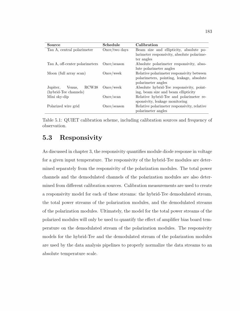
183
Source Schedule Calibration
Tau A, central polarimeter Once/two days Beam size and ellipticity, absolute po-larimeter responsivity, absolute polarime-ter angles
Tau A, off-center polarimeters Once/season Absolute polarimeter responsivity, abso-lute polarimeter angles
Moon (full array scan) Once/week Relative polarimeter responsivity betweenpolarimeters, pointing, leakage, absolutepolarimeter angles
Jupiter, Venus, RCW38(hybrid-Tee channels)
Once/week Absolute hybrid-Tee responsivity, point-ing, beam size and beam ellipticity
Mini sky-dip Once/scan Relative hybrid-Tee and polarimeter re-sponsivity, leakage monitoring
Polarized wire grid Once/season Relative polarimeter responsivity, relativepolarimeter angles
Table 5.1: QUIET calibration scheme, including calibration sources and frequency ofobservation.
5.3 Responsivity
As discussed in chapter 3, the responsivity quantifies module diode response in voltage
for a given input temperature. The responsivity of the hybrid-Tee modules are deter-
mined separately from the responsivity of the polarization modules. The total power
channels and the demodulated channels of the polarization modules are also deter-
mined from different calibration sources. Calibration measurements are used to create
a responsivity model for each of these streams: the hybrid-Tee demodulated stream,
the total power streams of the polarization modules, and the demodulated streams
of the polarization modules. Ultimately, the model for the total power streams of the
polarized modules will only be used to quantify the effect of amplifier bias board tem-
perature on the demodulated stream of the polarization modules. The responsivity
models for the hybrid-Tee and the demodulated stream of the polarization modules
are used by the data analysis pipelines to properly normalize the data streams to an
absolute temperature scale.
184
5.3.1 Total Power Responsivity
As described in section 2.5.4, the responsivity of all data streams (demodulated and
total power of the polarization and hybrid-Tee modules) depends on the amplifier
bias, which is strongly dependent on the temperature of the bias boards, such that
the dominant time-varying contribution to responsivity is the enclosure temperature.
The responsivity model must account for this dependence.
During the course of a mini sky-dip measurement, the modules will observe a
greater column density of atmosphere (and greater sky temperature) as the telescope
ranges from high to low elevation. With an atmospheric model (Ref. [72]) to determine
the sky temperature, the change in sky temperature during the mini sky-dip is used to
obtain total power responsivity. We perform mini sky-dips prior to each CES, yielding
a large statistical sample which can be used to probe the change in the responsivity
with enclosure temperature. We do not rely on knowing the sky temperature for our
absolute calibration.
We fit simultaneously for the zenith temperature from Jupiter measurements and
obtain coefficients of gain variation with enclosure temperature for each diode from
skydip measurements. The resulting model contains the fiducial responsivity value R0
for each diode, which represents the responsivity of the diode at the typical regulating
value of Tenc = 25C whose magnitude is calibrated to Jupiter, and the parameter
α which characterizes the dependence of the responsivity on enclosure temperature.
The average value of R0 for all diodes is 2.26 mV/K, typical uncertainties from the
fitting are 0.1mV/K. This is consistent with laboratory measurements of module
responsivity (section 3.4). The systematic error incurred from uncertainties in these
quantities will be discussed below.
185
5.3.2 Polarization Responsivity
The atmosphere is nearly linearly unpolarized ( 1%, Ref. [34]), such that the at-
mospheric temperature, PWV, and zenith temperature do not need to be considered
in the polarized gain model. In the case where the responsivitys in the two legs of
the module are equal, we expect that the responsivity, and also the dependence of
responsivity on Tenc (α), to be identical between the polarization and total power
streams. Because we bias the modules so that the responsivites in each leg balanced,
we can use the α values measured for the total power stream for the demodulated
stream as well. This approximation has also been confirmed from laboratory testing;
we monitored the response of the total power and demodulated streams while varying
the enclosure temperature and found the coefficients α were consistent between the
two streams.
The absolute responsivity values for the polarized data stream are obtained from
the polarized calibrator Tau A for the central polarimeter. We use the relative calibra-
tion measurements of all polarimeters of the Moon to obtain scaling factors between
the central polarimeter and all other polarimeters, and hence obtain absolute respon-
sivity values for the other polarimeters. This scaling factor was confirmed with the
wire-grid measurement performed once at the end of the season. The average values
of R0 (the responsivity for the demodulated stream at an enclosure temperature of
25C) for all diodes is 2.29 mV/K with similar fitting uncertainties as the total power
responsivity values for R0. The R0 values are consistent with the R0 values for the
total power stream for each diode.
5.3.3 Systematic Error Assessment
The primary science channel for QUIET is the demodulated stream, the total power
responsivity model functioned primarily to solve for the coefficients α, the change
in responsivity with respect to enclosure temperature. Thus systematic errors are
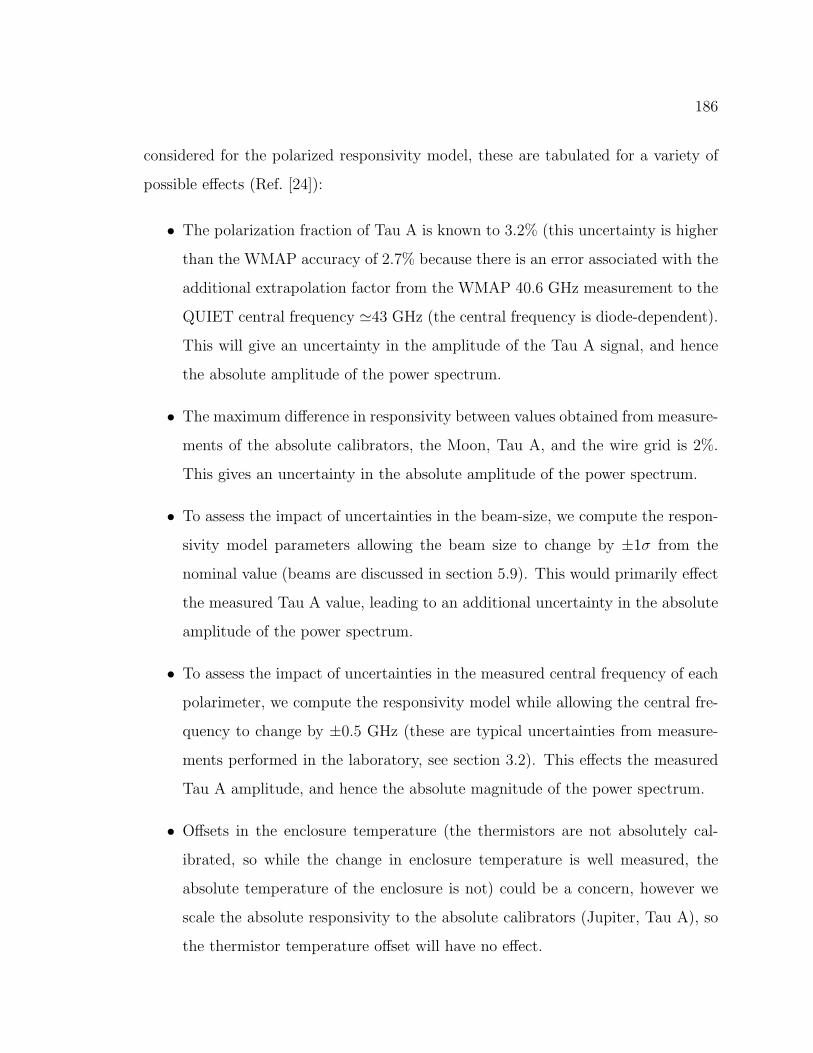
186
considered for the polarized responsivity model, these are tabulated for a variety of
possible effects (Ref. [24]):
• The polarization fraction of Tau A is known to 3.2% (this uncertainty is higher
than the WMAP accuracy of 2.7% because there is an error associated with the
additional extrapolation factor from the WMAP 40.6 GHz measurement to the
QUIET central frequency 43 GHz (the central frequency is diode-dependent).
This will give an uncertainty in the amplitude of the Tau A signal, and hence
the absolute amplitude of the power spectrum.
• The maximum difference in responsivity between values obtained from measure-
ments of the absolute calibrators, the Moon, Tau A, and the wire grid is 2%.
This gives an uncertainty in the absolute amplitude of the power spectrum.
• To assess the impact of uncertainties in the beam-size, we compute the respon-
sivity model parameters allowing the beam size to change by ±1σ from the
nominal value (beams are discussed in section 5.9). This would primarily effect
the measured Tau A value, leading to an additional uncertainty in the absolute
amplitude of the power spectrum.
• To assess the impact of uncertainties in the measured central frequency of each
polarimeter, we compute the responsivity model while allowing the central fre-
quency to change by ±0.5 GHz (these are typical uncertainties from measure-
ments performed in the laboratory, see section 3.2). This effects the measured
Tau A amplitude, and hence the absolute magnitude of the power spectrum.
• Offsets in the enclosure temperature (the thermistors are not absolutely cal-
ibrated, so while the change in enclosure temperature is well measured, the
absolute temperature of the enclosure is not) could be a concern, however we
scale the absolute responsivity to the absolute calibrators (Jupiter, Tau A), so
the thermistor temperature offset will have no effect.
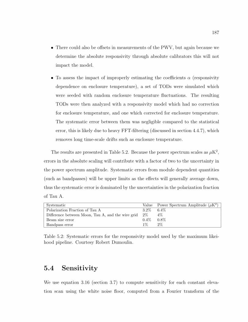
187
• There could also be offsets in measurements of the PWV, but again because we
determine the absolute responsivity through absolute calibrators this will not
impact the model.
• To assess the impact of improperly estimating the coefficients α (responsivity
dependence on enclosure temperature), a set of TODs were simulated which
were seeded with random enclosure temperature fluctuations. The resulting
TODs were then analyzed with a responsivity model which had no correction
for enclosure temperature, and one which corrected for enclosure temperature.
The systematic error between them was negligible compared to the statistical
error, this is likely due to heavy FFT-filtering (discussed in section 4.4.7), which
removes long time-scale drifts such as enclosure temperature.
The results are presented in Table 5.2. Because the power spectrum scales as µK2,
errors in the absolute scaling will contribute with a factor of two to the uncertainty in
the power spectrum amplitude. Systematic errors from module dependent quantities
(such as bandpasses) will be upper limits as the effects will generally average down,
thus the systematic error is dominated by the uncertainties in the polarization fraction
of Tau A.
Systematic Value Power Spectrum Amplitude (µK2)Polarization Fraction of Tau A 3.2% 6.4%Difference between Moon, Tau A, and the wire grid 2% 4%Beam size error 0.4% 0.8%Bandpass error 1% 2%
Table 5.2: Systematic errors for the responsivity model used by the maximum likei-hood pipeline. Courtesy Robert Dumoulin.
5.4 Sensitivity
We use equation 3.16 (section 3.7) to compute sensitivity for each constant eleva-
tion scan using the white noise floor, computed from a Fourier transform of the
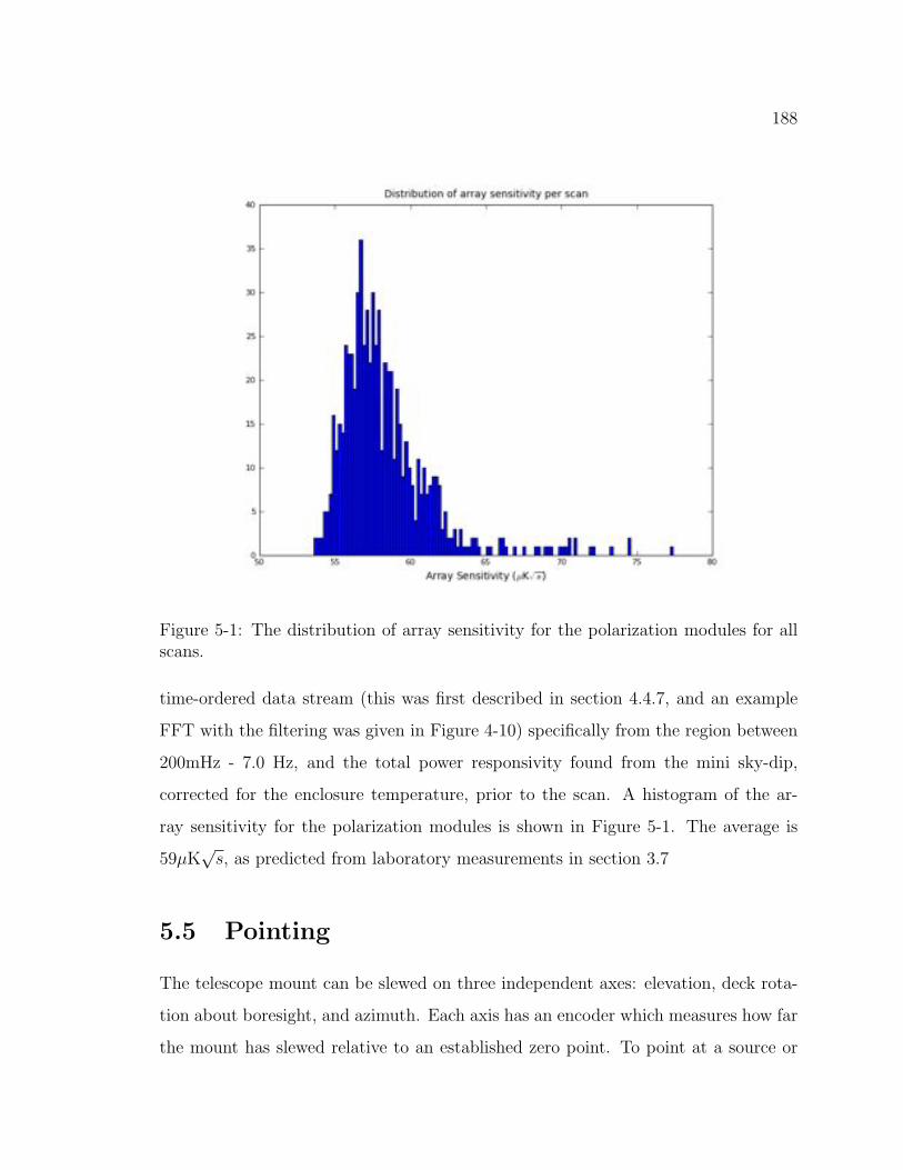
188
Figure 5-1: The distribution of array sensitivity for the polarization modules for allscans.
time-ordered data stream (this was first described in section 4.4.7, and an example
FFT with the filtering was given in Figure 4-10) specifically from the region between
200mHz - 7.0 Hz, and the total power responsivity found from the mini sky-dip,
corrected for the enclosure temperature, prior to the scan. A histogram of the ar-
ray sensitivity for the polarization modules is shown in Figure 5-1. The average is
59µK√
s, as predicted from laboratory measurements in section 3.7
5.5 Pointing
The telescope mount can be slewed on three independent axes: elevation, deck rota-
tion about boresight, and azimuth. Each axis has an encoder which measures how far
the mount has slewed relative to an established zero point. To point at a source or
189
scan a patch, we obtain the ephemeris position of a source in azimuth and elevation,
slew the telescope to that azimuth and elevation location, and the source should ap-
pear in the beam of the central polarimeter. Various non-idealities and offsets within
the mount require that we create a pointing mount model to account for these off-
sets. These include flexure and tilting (kf , ∆HA, ∆φA, ΘE); the offset between the
boresight pointing of the receiver and the rotation axis of the telescope (Θc and Φc);
and encoder offsets (E0, A0, and P0, ∆D) (Ref. [70]). These are described in more
detail below. We do not present the full mount model here (details can be found in
Ref. [8]), and just note that the mount model consists of a set of equations which
use the above parameters to allow us to accurately point the boresight of the receiver
beam at a target.
• kf - Constant of flexure (degree per cosine of elevation).
• ∆HA - The tilt of the azimuth axis in the direction of increasing hour angle.
• ∆φA - The tilt of the azimuth axis in the direction of increasing latitude.
• ΘE - The tilt of the elevation axis perpendicular to the azimuth tilt, measured
clockwise around the direction of the azimuth vector.
• Θc - The magnitude of the collimation error, defined as the distance between
the boresight of the telescope and the central polarimeter pointing.
• Φc - The deck angle at which the collimation error is directed radially outward.
• E0 - The elevation encoder count at zero azimuth.
• A0 - The azimuth encoder count at zero azimuth.
• P0 - The deck encoder count that aligns the reference edge of the triangular
platform to be horizontal. The reference edge should be chosen such that P0 is
close to zero.
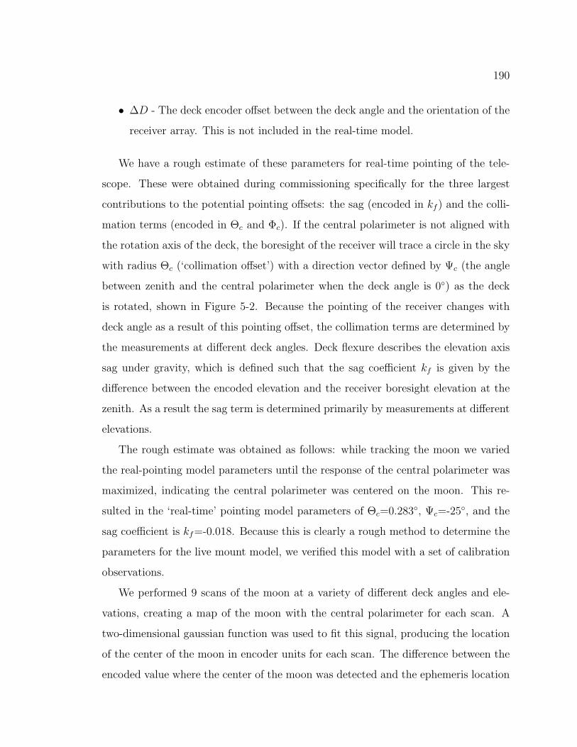
190
• ∆D - The deck encoder offset between the deck angle and the orientation of the
receiver array. This is not included in the real-time model.
We have a rough estimate of these parameters for real-time pointing of the tele-
scope. These were obtained during commissioning specifically for the three largest
contributions to the potential pointing offsets: the sag (encoded in kf ) and the colli-
mation terms (encoded in Θc and Φc). If the central polarimeter is not aligned with
the rotation axis of the deck, the boresight of the receiver will trace a circle in the sky
with radius Θc (‘collimation offset’) with a direction vector defined by Ψc (the angle
between zenith and the central polarimeter when the deck angle is 0) as the deck
is rotated, shown in Figure 5-2. Because the pointing of the receiver changes with
deck angle as a result of this pointing offset, the collimation terms are determined by
the measurements at different deck angles. Deck flexure describes the elevation axis
sag under gravity, which is defined such that the sag coefficient kf is given by the
difference between the encoded elevation and the receiver boresight elevation at the
zenith. As a result the sag term is determined primarily by measurements at different
elevations.
The rough estimate was obtained as follows: while tracking the moon we varied
the real-pointing model parameters until the response of the central polarimeter was
maximized, indicating the central polarimeter was centered on the moon. This re-
sulted in the ‘real-time’ pointing model parameters of Θc=0.283, Ψc=-25, and the
sag coefficient is kf=-0.018. Because this is clearly a rough method to determine the
parameters for the live mount model, we verified this model with a set of calibration
observations.
We performed 9 scans of the moon at a variety of different deck angles and ele-
vations, creating a map of the moon with the central polarimeter for each scan. A
two-dimensional gaussian function was used to fit this signal, producing the location
of the center of the moon in encoder units for each scan. The difference between the
encoded value where the center of the moon was detected and the ephemeris location
191
Figure 5-2: Illustration of the collimation offset parameters (Θc, Ψc). In this illustra-tion, the mount is at the center of the sphere, the azimuth axis is denoted by A and isparallel with the horizon. The elevation axis is perpendicular to this and is denotedby E. The telescope is pointed to A
and E at a deck angle given by γ. While the
telescope is pointed at A and E
, the source is observed by the receiver to be locatedat A and E. The collimation offset is then clearly seen to be the radial distance be-tween the telescope pointing and the location where the source was observed by thereceiver and the collimation angle is defined by the elevation axis. Courtesy MartinShepherd.
of the moon gives the pointing offset.
We simultaneously fit the three mount-model parameters with nine measurements
using a non-linear least squares fitting algorithm. The best-fit values are Θc=0.268
+/- 0.01, Ψc=-27.4 +/- 1.8, and kf=-1×10⁻³ +/- 5.8×10⁻⁴. The residuals between
the real-time-pointing mount model used by the telescope and the best-fit values for
the mount model parameters are 1.8 arcmin, less than 1/10 of our beamsize. The real-
time model was deemed sufficient for use by the telescope for science observations.
192
Because we had started science observations slightly before the mount was verified,
we kept using the mount model parameters from the rough fit, noting we incur an
acceptable pointing error from doing so.
We refine the mount model parameters for the purposes of map-making, which
will use the encoded values of azimuth, elevation, and deck to determine the pointing
on the sky of each polarimeter in the array. The Maximum Likelihood pipeline uses
Jupiter and Venus observations to fit for the mount model parameters throughout
the season (the scans were described in section 5.2.1). The Jupiter observations are
particularly useful for pointing because Jupiter is point-like at the Q-band beam
resolution, and because the hybrid-Tee polarimeters used for Jupiter observations are
located 4 away from the boresight, providing a larger lever arm for determining our
pointing accuracy in certain mount model parameters. The current working mount
model gives pointing residuals of 3.5 arcminutes, slightly larger than the pointing
accuracy goal but not enough to compromise the Q-band Phase-I science goals.
Deck Encoder Slip
The deck-angle encoder was loose from the start of observations until January 28, 2009
when the situation was discovered and the encoder bolts were tightened. This caused
the recorded deck position to vary such that there can be an error in the relationship
between the encoder value and the true deck orientation. We quantified the magnitude
of the encoder errors using moon measurements: because we scan over the moon with
all polarimeters during the course of one moon calibration observations, the difference
between the ephemeris position of the moon and the encoded position where each
polarimeter saw the moon results in an absolute pointing for each polarimeter, and
an absolute orientation of the array on the sky. This orientation can be compared to
the encoded value of the deck angle. A similar analysis can be performed with the two
hybrid-Tee modules using the calibration sources Venus, Jupiter, and RCW38. We
found the deck angle encoder value jumped occasionally by 2, as seen in Figure 5-
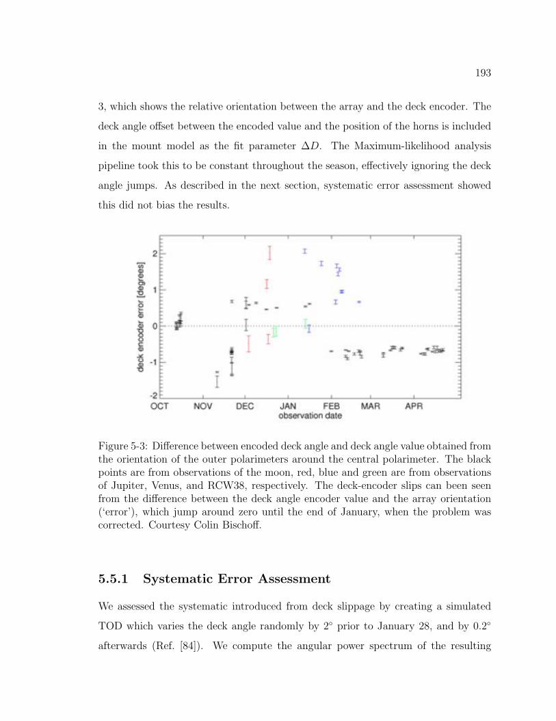
193
3, which shows the relative orientation between the array and the deck encoder. The
deck angle offset between the encoded value and the position of the horns is included
in the mount model as the fit parameter ∆D. The Maximum-likelihood analysis
pipeline took this to be constant throughout the season, effectively ignoring the deck
angle jumps. As described in the next section, systematic error assessment showed
this did not bias the results.
Figure 5-3: Difference between encoded deck angle and deck angle value obtained fromthe orientation of the outer polarimeters around the central polarimeter. The blackpoints are from observations of the moon, red, blue and green are from observationsof Jupiter, Venus, and RCW38, respectively. The deck-encoder slips can been seenfrom the difference between the deck angle encoder value and the array orientation(‘error’), which jump around zero until the end of January, when the problem wascorrected. Courtesy Colin Bischoff.
5.5.1 Systematic Error Assessment
We assessed the systematic introduced from deck slippage by creating a simulated
TOD which varies the deck angle randomly by 2 prior to January 28, and by 0.2
afterwards (Ref. [84]). We compute the angular power spectrum of the resulting

194
TODs, and compare it to a spectrum without these deck angle slips to quantify
the effect on the final CMB angular power spectrum from the deck slippage. The
QUIET noise level and scanning strategy are included in the simulated TODs. The
results are included in Table 5.5; the systematic errors are 66% of the statistical
errors. While this indicates the systematic is subdominant to the statistical error,
additional investigations are being considered to assess whether this is a possible
source of systematic bias.
5.6 Timing
The timing card in the receiver electronics enclosure obtains time-stamps from the
telescope, and time stamps in the receiver data. However, the time-stamps are not
necessarily aligned due to time lags from board processing. To measure the time lag
between the receiver and telescope pointing, we performed azimuth slews across the
moon: one a forward-going slew, the other a backward-going slew. We repeated these
measurements a different slewing speeds: 1.5, 2.8, and 6 /s; (6/s is the slewing speed
for CMB scans, the other two were chosen to be as different as possible because we
were not sure of the origin of the timing lags). The methodology for this measurement
is shown schematically in Figure 5-4, where ABoresight is the telescope azimuth encoder
position at a given time, and AMoon is the azimuth ephemeris position of the moon.
As the telescope performs a slew across the moon, the boresight pointing will
correspond to the ephemeris location of the moon at some time stamp t. If the receiver
time stamp is advanced from the telescope by ∆t, then the receiver will register the
moon at time stamp t+∆t. However, the telescope pointing ABoresight at time stamp
t + ∆t will have already passed the moon, giving ABoresight − AMoon > 0 when the
receiver registers the signal (this scenario is shown for a forward-going slew in the
upper panel of Figure 5-4). The opposite will be true for the backward-going slew,
shown in the lower panel of Figure 5-4. The difference in azimuth ABoresight −AMoon
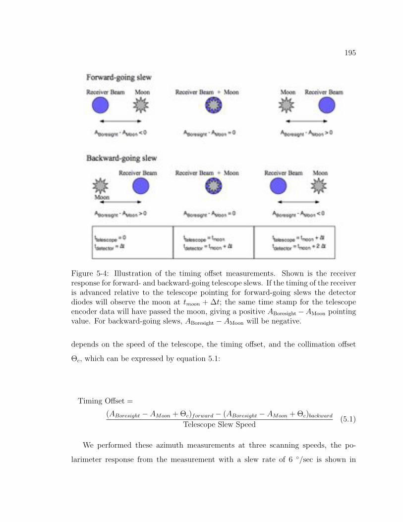
195
Figure 5-4: Illustration of the timing offset measurements. Shown is the receiverresponse for forward- and backward-going telescope slews. If the timing of the receiveris advanced relative to the telescope pointing for forward-going slews the detectordiodes will observe the moon at tmoon + ∆t; the same time stamp for the telescopeencoder data will have passed the moon, giving a positive ABoresight−AMoon pointingvalue. For backward-going slews, ABoresight − AMoon will be negative.
depends on the speed of the telescope, the timing offset, and the collimation offset
Θc, which can be expressed by equation 5.1:
Timing Offset =
(ABoresight − AMoon + Θc)forward − (ABoresight − AMoon + Θc)backward
Telescope Slew Speed(5.1)
We performed these azimuth measurements at three scanning speeds, the po-
larimeter response from the measurement with a slew rate of 6 /sec is shown in
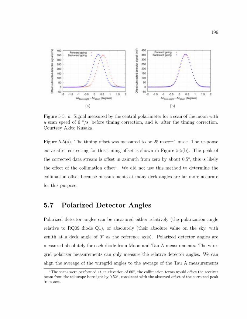
196
(a) (b)
Figure 5-5: a: Signal measured by the central polarimeter for a scan of the moon witha scan speed of 6 /s, before timing correction, and b: after the timing correction.Courtsey Akito Kusaka.
Figure 5-5(a). The timing offset was measured to be 25 msec±1 msec. The response
curve after correcting for this timing offset is shown in Figure 5-5(b). The peak of
the corrected data stream is offset in azimuth from zero by about 0.5, this is likely
the effect of the collimation offset1. We did not use this method to determine the
collimation offset because measurements at many deck angles are far more accurate
for this purpose.
5.7 Polarized Detector Angles
Polarized detector angles can be measured either relatively (the polarization angle
relative to RQ09 diode Q1), or absolutely (their absolute value on the sky, with
zenith at a deck angle of 0 as the reference axis). Polarized detector angles are
measured absolutely for each diode from Moon and Tau A measurements. The wire-
grid polarizer measurements can only measure the relative detector angles. We can
align the average of the wiregrid angles to the average of the Tau A measurements
1The scans were performed at an elevation of 60, the collimation terms would offset the receiverbeam from the telescope boresight by 0.52, consistent with the observed offset of the corrected peakfrom zero.
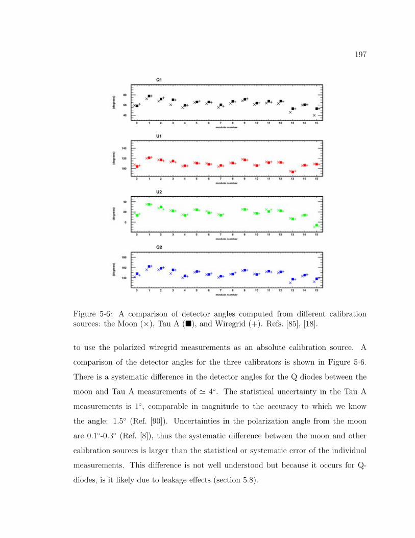
197
Figure 5-6: A comparison of detector angles computed from different calibrationsources: the Moon (×), Tau A (), and Wiregrid (+). Refs. [85], [18].
to use the polarized wiregrid measurements as an absolute calibration source. A
comparison of the detector angles for the three calibrators is shown in Figure 5-6.
There is a systematic difference in the detector angles for the Q diodes between the
moon and Tau A measurements of 4. The statistical uncertainty in the Tau A
measurements is 1, comparable in magnitude to the accuracy to which we know
the angle: 1.5 (Ref. [90]). Uncertainties in the polarization angle from the moon
are 0.1-0.3 (Ref. [8]), thus the systematic difference between the moon and other
calibration sources is larger than the statistical or systematic error of the individual
measurements. This difference is not well understood but because it occurs for Q-
diodes, is it likely due to leakage effects (section 5.8).
198
5.7.1 Systematic Error Assessment
Systematic errors were assessed between the different calibration sources by gener-
ating simulated TOD data using angles measured from Tau A and the wire grid
polarizer, and then analyzing the TOD samples using the angles measured by the
moon (Refs. [85], [18]). The QUIET noise level and scanning strategy are included
in the simulated TODs. The resulting estimate of the effect on the power spectrum
from the systematic differences in detector angles between calibration sources shows
systematic errors which are 10% of the statistical errors for the EE and BB spectra
at an of 300. This systematic will produce a minimum constraint QUIET can place
on the tensor-to-scalar ratio of r 0.1.
5.8 Leakage
As discussed in section 2.2, the OMT-module system has leakage from total power to
polarization; this will cause the CMB temperature signal to leak into the polarization
maps. This leakage is mitigated by observing at multiple deck angles as the leakage
signal will average down as the leakage map rotates with the deck. Leakage is mea-
sured for each diode with a variety of calibrators, and is expressed as a coefficient
representing the amount of polarized emission a detector diode would measure from
an unpolarized source.
• The moon We use a model developed within the collaboration (Ref. [8]) of
the moon, which provides both an intensity and polarization template. Any
polarization measured which is not predicted by the model is considered leakage,
and from this a leakage coefficient is obtained.
• Tau A We adopt the WMAP (Ref. [90]) polarization fraction, angles, and
the total power signal of Tau A; any additional measured polarized signal is
classified as leakage.
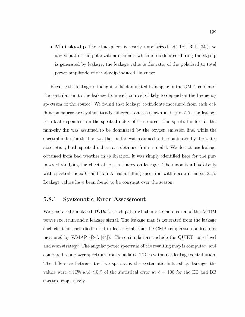
199
• Mini sky-dip The atmosphere is nearly unpolarized ( 1%, Ref. [34]), so
any signal in the polarization channels which is modulated during the skydip
is generated by leakage; the leakage value is the ratio of the polarized to total
power amplitude of the skydip induced sin curve.
Because the leakage is thought to be dominated by a spike in the OMT bandpass,
the contribution to the leakage from each source is likely to depend on the frequency
spectrum of the source. We found that leakage coefficients measured from each cal-
ibration source are systematically different, and as shown in Figure 5-7, the leakage
is in fact dependent on the spectral index of the source. The spectral index for the
mini-sky dip was assumed to be dominated by the oxygen emission line, while the
spectral index for the bad-weather period was assumed to be dominated by the water
absorption; both spectral indices are obtained from a model. We do not use leakage
obtained from bad weather in calibration, it was simply identified here for the pur-
poses of studying the effect of spectral index on leakage. The moon is a black-body
with spectral index 0, and Tau A has a falling spectrum with spectral index -2.35.
Leakage values have been found to be constant over the season.
5.8.1 Systematic Error Assessment
We generated simulated TODs for each patch which are a combination of the ΛCDM
power spectrum and a leakage signal. The leakage map is generated from the leakage
coefficient for each diode used to leak signal from the CMB temperature anisotropy
measured by WMAP (Ref. [44]). These simulations include the QUIET noise level
and scan strategy. The angular power spectrum of the resulting map is computed, and
compared to a power spectrum from simulated TODs without a leakage contribution.
The difference between the two spectra is the systematic induced by leakage, the
values were 10% and 5% of the statistical error at = 100 for the EE and BB
spectra, respectively.
200
Figure 5-7: The upper panel shows a comparison of leakage coefficients as measuredby a mini sky-dip (), a sky-dip (), bad weather (), the Moon (•), and Tau A(+),in order of spectral index for diode Q1. The other panels show the three diodes U1,U2, and Q2. The atmosphere has a spectral index which increases with frequency:β > 0. Bad weather will have a higher water vapor content, which has a gentler slopethan the atmosphere.Courtesy Osamu Tajima, Ref. [18].
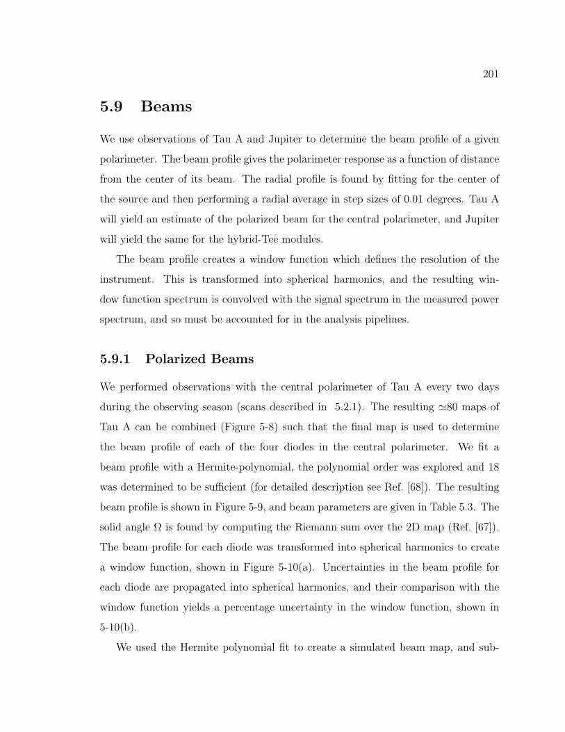
201
5.9 Beams
We use observations of Tau A and Jupiter to determine the beam profile of a given
polarimeter. The beam profile gives the polarimeter response as a function of distance
from the center of its beam. The radial profile is found by fitting for the center of
the source and then performing a radial average in step sizes of 0.01 degrees. Tau A
will yield an estimate of the polarized beam for the central polarimeter, and Jupiter
will yield the same for the hybrid-Tee modules.
The beam profile creates a window function which defines the resolution of the
instrument. This is transformed into spherical harmonics, and the resulting win-
dow function spectrum is convolved with the signal spectrum in the measured power
spectrum, and so must be accounted for in the analysis pipelines.
5.9.1 Polarized Beams
We performed observations with the central polarimeter of Tau A every two days
during the observing season (scans described in 5.2.1). The resulting 80 maps of
Tau A can be combined (Figure 5-8) such that the final map is used to determine
the beam profile of each of the four diodes in the central polarimeter. We fit a
beam profile with a Hermite-polynomial, the polynomial order was explored and 18
was determined to be sufficient (for detailed description see Ref. [68]). The resulting
beam profile is shown in Figure 5-9, and beam parameters are given in Table 5.3. The
solid angle Ω is found by computing the Riemann sum over the 2D map (Ref. [67]).
The beam profile for each diode was transformed into spherical harmonics to create
a window function, shown in Figure 5-10(a). Uncertainties in the beam profile for
each diode are propagated into spherical harmonics, and their comparison with the
window function yields a percentage uncertainty in the window function, shown in
5-10(b).
We used the Hermite polynomial fit to create a simulated beam map, and sub-
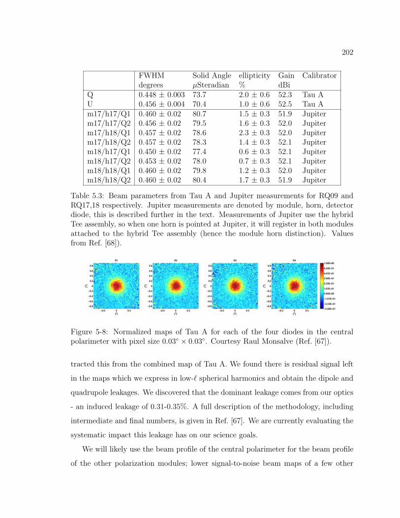
202
FWHM Solid Angle ellipticity Gain Calibratordegrees µSteradian % dBi
Q 0.448 ± 0.003 73.7 2.0 ± 0.6 52.3 Tau AU 0.456 ± 0.004 70.4 1.0 ± 0.6 52.5 Tau Am17/h17/Q1 0.460 ± 0.02 80.7 1.5 ± 0.3 51.9 Jupiterm17/h17/Q2 0.456 ± 0.02 79.5 1.6 ± 0.3 52.0 Jupiterm17/h18/Q1 0.457 ± 0.02 78.6 2.3 ± 0.3 52.0 Jupiterm17/h18/Q2 0.457 ± 0.02 78.3 1.4 ± 0.3 52.1 Jupiterm18/h17/Q1 0.450 ± 0.02 77.4 0.6 ± 0.3 52.1 Jupiterm18/h17/Q2 0.453 ± 0.02 78.0 0.7 ± 0.3 52.1 Jupiterm18/h18/Q1 0.460 ± 0.02 79.8 1.2 ± 0.3 52.0 Jupiterm18/h18/Q2 0.460 ± 0.02 80.4 1.7 ± 0.3 51.9 Jupiter
Table 5.3: Beam parameters from Tau A and Jupiter measurements for RQ09 andRQ17,18 respectively. Jupiter measurements are denoted by module, horn, detectordiode, this is described further in the text. Measurements of Jupiter use the hybridTee assembly, so when one horn is pointed at Jupiter, it will register in both modulesattached to the hybrid Tee assembly (hence the module horn distinction). Valuesfrom Ref. [68]).
Figure 5-8: Normalized maps of Tau A for each of the four diodes in the centralpolarimeter with pixel size 0.03 × 0.03. Courtesy Raul Monsalve (Ref. [67]).
tracted this from the combined map of Tau A. We found there is residual signal left
in the maps which we express in low- spherical harmonics and obtain the dipole and
quadrupole leakages. We discovered that the dominant leakage comes from our optics
- an induced leakage of 0.31-0.35%. A full description of the methodology, including
intermediate and final numbers, is given in Ref. [67]. We are currently evaluating the
systematic impact this leakage has on our science goals.
We will likely use the beam profile of the central polarimeter for the beam profile
of the other polarization modules; lower signal-to-noise beam maps of a few other
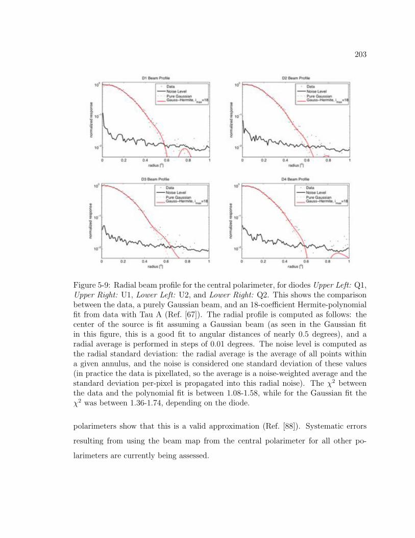
203
Figure 5-9: Radial beam profile for the central polarimeter, for diodes Upper Left: Q1,Upper Right: U1, Lower Left: U2, and Lower Right: Q2. This shows the comparisonbetween the data, a purely Gaussian beam, and an 18-coefficient Hermite-polynomialfit from data with Tau A (Ref. [67]). The radial profile is computed as follows: thecenter of the source is fit assuming a Gaussian beam (as seen in the Gaussian fitin this figure, this is a good fit to angular distances of nearly 0.5 degrees), and aradial average is performed in steps of 0.01 degrees. The noise level is computed asthe radial standard deviation: the radial average is the average of all points withina given annulus, and the noise is considered one standard deviation of these values(in practice the data is pixellated, so the average is a noise-weighted average and thestandard deviation per-pixel is propagated into this radial noise). The χ
2 betweenthe data and the polynomial fit is between 1.08-1.58, while for the Gaussian fit theχ
2 was between 1.36-1.74, depending on the diode.
polarimeters show that this is a valid approximation (Ref. [88]). Systematic errors
resulting from using the beam map from the central polarimeter for all other po-
larimeters are currently being assessed.
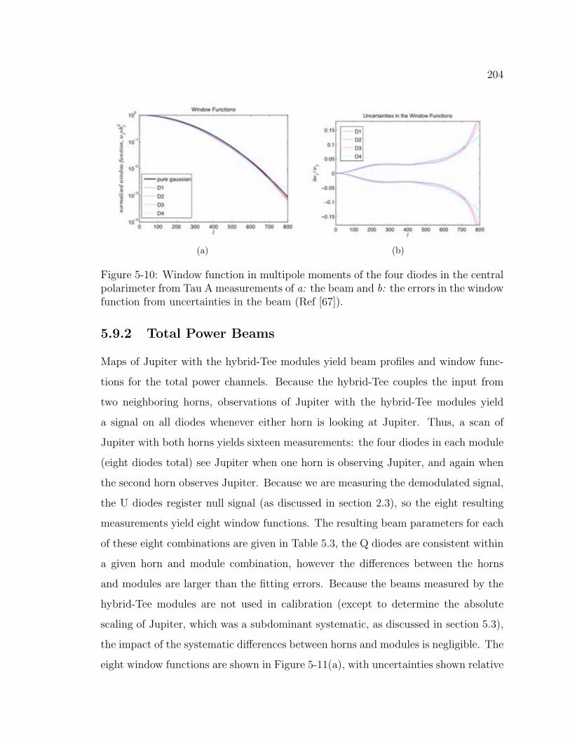
204
(a) (b)
Figure 5-10: Window function in multipole moments of the four diodes in the centralpolarimeter from Tau A measurements of a: the beam and b: the errors in the windowfunction from uncertainties in the beam (Ref [67]).
5.9.2 Total Power Beams
Maps of Jupiter with the hybrid-Tee modules yield beam profiles and window func-
tions for the total power channels. Because the hybrid-Tee couples the input from
two neighboring horns, observations of Jupiter with the hybrid-Tee modules yield
a signal on all diodes whenever either horn is looking at Jupiter. Thus, a scan of
Jupiter with both horns yields sixteen measurements: the four diodes in each module
(eight diodes total) see Jupiter when one horn is observing Jupiter, and again when
the second horn observes Jupiter. Because we are measuring the demodulated signal,
the U diodes register null signal (as discussed in section 2.3), so the eight resulting
measurements yield eight window functions. The resulting beam parameters for each
of these eight combinations are given in Table 5.3, the Q diodes are consistent within
a given horn and module combination, however the differences between the horns
and modules are larger than the fitting errors. Because the beams measured by the
hybrid-Tee modules are not used in calibration (except to determine the absolute
scaling of Jupiter, which was a subdominant systematic, as discussed in section 5.3),
the impact of the systematic differences between horns and modules is negligible. The
eight window functions are shown in Figure 5-11(a), with uncertainties shown relative
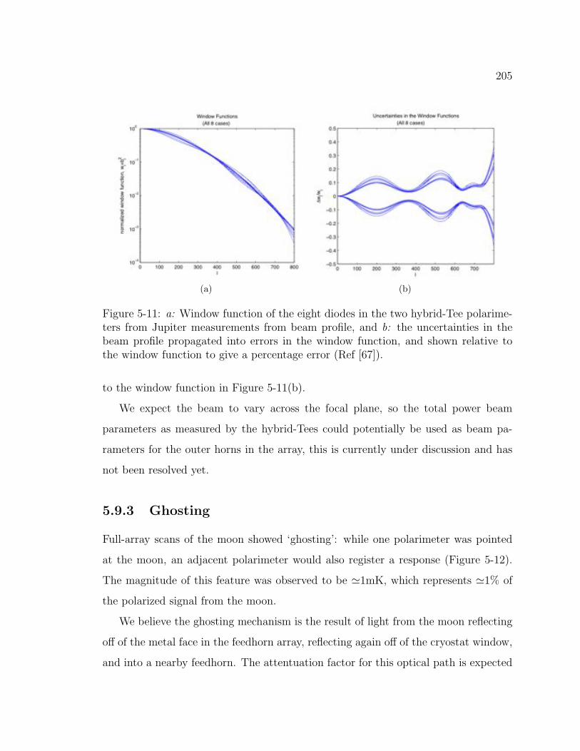
205
(a) (b)
Figure 5-11: a: Window function of the eight diodes in the two hybrid-Tee polarime-ters from Jupiter measurements from beam profile, and b: the uncertainties in thebeam profile propagated into errors in the window function, and shown relative tothe window function to give a percentage error (Ref [67]).
to the window function in Figure 5-11(b).
We expect the beam to vary across the focal plane, so the total power beam
parameters as measured by the hybrid-Tees could potentially be used as beam pa-
rameters for the outer horns in the array, this is currently under discussion and has
not been resolved yet.
5.9.3 Ghosting
Full-array scans of the moon showed ‘ghosting’: while one polarimeter was pointed
at the moon, an adjacent polarimeter would also register a response (Figure 5-12).
The magnitude of this feature was observed to be 1mK, which represents 1% of
the polarized signal from the moon.
We believe the ghosting mechanism is the result of light from the moon reflecting
off of the metal face in the feedhorn array, reflecting again off of the cryostat window,
and into a nearby feedhorn. The attentuation factor for this optical path is expected
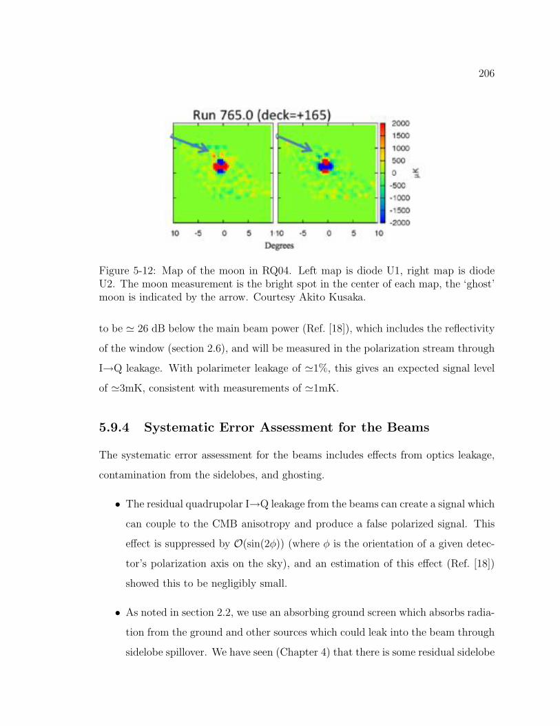
206
Figure 5-12: Map of the moon in RQ04. Left map is diode U1, right map is diodeU2. The moon measurement is the bright spot in the center of each map, the ‘ghost’moon is indicated by the arrow. Courtesy Akito Kusaka.
to be 26 dB below the main beam power (Ref. [18]), which includes the reflectivity
of the window (section 2.6), and will be measured in the polarization stream through
I→Q leakage. With polarimeter leakage of 1%, this gives an expected signal level
of 3mK, consistent with measurements of 1mK.
5.9.4 Systematic Error Assessment for the Beams
The systematic error assessment for the beams includes effects from optics leakage,
contamination from the sidelobes, and ghosting.
• The residual quadrupolar I→Q leakage from the beams can create a signal which
can couple to the CMB anisotropy and produce a false polarized signal. This
effect is suppressed by O(sin(2φ)) (where φ is the orientation of a given detec-
tor’s polarization axis on the sky), and an estimation of this effect (Ref. [18])
showed this to be negligibly small.
• As noted in section 2.2, we use an absorbing ground screen which absorbs radia-
tion from the ground and other sources which could leak into the beam through
sidelobe spillover. We have seen (Chapter 4) that there is some residual sidelobe
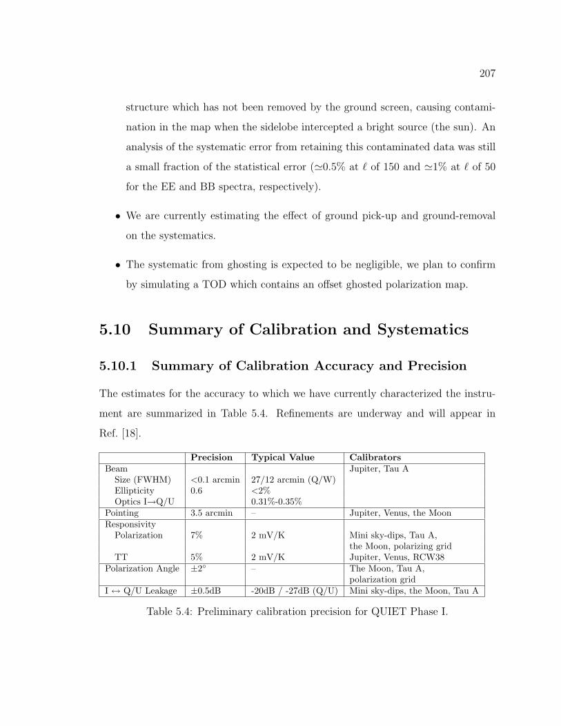
207
structure which has not been removed by the ground screen, causing contami-
nation in the map when the sidelobe intercepted a bright source (the sun). An
analysis of the systematic error from retaining this contaminated data was still
a small fraction of the statistical error (0.5% at of 150 and 1% at of 50
for the EE and BB spectra, respectively).
• We are currently estimating the effect of ground pick-up and ground-removal
on the systematics.
• The systematic from ghosting is expected to be negligible, we plan to confirm
by simulating a TOD which contains an offset ghosted polarization map.
5.10 Summary of Calibration and Systematics
5.10.1 Summary of Calibration Accuracy and Precision
The estimates for the accuracy to which we have currently characterized the instru-
ment are summarized in Table 5.4. Refinements are underway and will appear in
Ref. [18].
Precision Typical Value Calibrators
Beam Jupiter, Tau ASize (FWHM) <0.1 arcmin 27/12 arcmin (Q/W)Ellipticity 0.6 <2%Optics I→Q/U 0.31%-0.35%
Pointing 3.5 arcmin – Jupiter, Venus, the MoonResponsivity
Polarization 7% 2 mV/K Mini sky-dips, Tau A,the Moon, polarizing grid
TT 5% 2 mV/K Jupiter, Venus, RCW38Polarization Angle ±2 – The Moon, Tau A,
polarization gridI ↔ Q/U Leakage ±0.5dB -20dB / -27dB (Q/U) Mini sky-dips, the Moon, Tau A
Table 5.4: Preliminary calibration precision for QUIET Phase I.
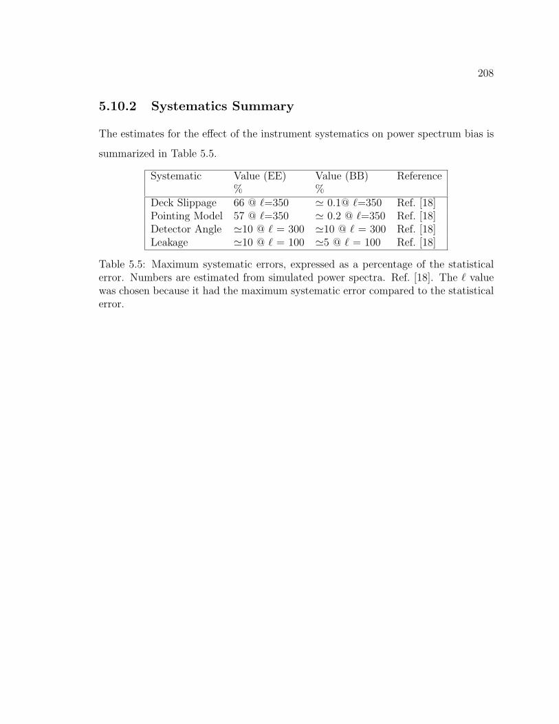
208
5.10.2 Systematics Summary
The estimates for the effect of the instrument systematics on power spectrum bias is
summarized in Table 5.5.
Systematic Value (EE) Value (BB) Reference% %
Deck Slippage 66 @ =350 0.1@ =350 Ref. [18]Pointing Model 57 @ =350 0.2 @ =350 Ref. [18]Detector Angle 10 @ = 300 10 @ = 300 Ref. [18]Leakage 10 @ = 100 5 @ = 100 Ref. [18]
Table 5.5: Maximum systematic errors, expressed as a percentage of the statisticalerror. Numbers are estimated from simulated power spectra. Ref. [18]. The valuewas chosen because it had the maximum systematic error compared to the statisticalerror.
Chapter 6
CMB Power Spectrum Analysis
and Results With a Maximum
Likelihood Pipeline
6.1 Introduction
We employ two independent analysis pipelines for CMB map-making and power spec-
trum estimation for the QUIET data set. This chapter addresses the Maximum-
likelihood data analysis pipeline methodology, applications, and some preliminary
results.
6.2 Maximum-Likelihood Method Background
The Maximum-likelihood method is a parameter-estimation algorithm based on Bayes
theorem, which describes the probability distribution of a set of parameters Θ and
assumptions I in a model given a data set D and an initial estimate for the likeliness
of the model and parameters. This is described by the posterior, given by one form
of Bayes’ Theorem (see e.g Ref. [80]):
209
210
P (Θ|D, I) ∝ P (D|Θ)P (Θ|I) (6.1)
Where P (Θ|D, I) is the posterior, P (D|Θ) is the ‘likelihood’, which describes the
probability of the data given a set of parameters (generally this is what one mea-
sures), and P (Θ|I) is the ‘prior’, which encodes what one already knows about the
parameters. If the prior as taken as uniform, then maximizing the likelihood will also
maximize the posterior, yielding a distribution for each Θ from which one can find
the most probable set of Θ to describe the data with the chosen model. The form of
the likelihood depends on the model one is testing.
We use the Maximum-likelihood formalism in the Maximum-likelihood pipeline
both for map-making and for power spectrum estimation.
6.3 Optimal Map Making
The Maximum-likelihood pipeline uses an “optimal” map-maker, defined by (Ref. [38]):
dp =P
†ptN
−1
tt Ptp
−1
P†ptN
−1
tt dt (6.2)
where dt is a data point at a given time t, dp is the map pixel which that data
point will map to, P is the pointing matrix, and N−1
tt is the inverse of the noise-
covariance matrix, which describes noise correlation between noise n at times t and
t: Ntt = n(t)n(t). Functionally we compute the pixel-pixel covariance matrix,
which is simply the first term in brackets: N−1
pp =P
†ptN
−1
tt Ptp
−1
. As was shown in
Ref. [86], the mapmaking formalism described by equation 6.2 minimizes the residuals
between the true map and the reconstructed map (known as minimum variance) and
the map itself is lossless and unbiased. It is also the Maximum-likelihood estimate if
211
the noise is approximately Gaussian.
The pointing matrix P maps a point in the sky to a time and includes the pointing
model, the polarimeter polarization angles for each detector diode, and the respon-
sivity model. The inverse noise covariance matrix is formed from the noise model,
discussed in section 4.4.7. It includes white noise diode-diode correlation coefficients
(discussed in section 2.3.5), which are computed for each CES via:
ρx,y =cov(x, y)
σxσy(6.3)
=< (x− x)(y − y) >
σxσy(6.4)
=< xy > − < x >< y >
σxσy(6.5)
where x and y are the diode TODs, such that there is one correlation coefficient
for each diode pair, per module, for each scan. The correlated noise between Q-
and U- diodes in a single polarimeter can be in excess of 30% of the theoretical
expectation. As long as this value is properly accounted for in the noise model this
excess correlation has no effect on the data. The correlations do not extend to low
frequencies in the 1/f portion of the noise power spectrum, so noise at frequencies
lower than the knee frequency is modeled as uncorrelated, while noise in the white-
noise regime is modeled as correlated. Implicit in the 1/f model is that the noise
is stationary throughout one constant elevation scan such that we use one value to
characterize the noise, we have found this to be a reasonable approximation in most
cases. In theory, the noise covariance matrix should retain elements for all pairs of
(t,t) over the entire observing season; in practice we use the noise power spectrum
to determine the time interval necessary to achieve a desired accuracy in the noise
matrix. We find that this is typically between 20–200 seconds.
Each CMB constant-elevation scan will produce two minimum variance maps and
noise covariance matrices, one for the Stokes Q and another for the Stokes U param-
eters. The CES maps which pass data selection (discussed in chapter 4) are then
212
averaged together separately for the Q and U diodes, pixel-by-pixel, and the contri-
bution to the final map is weighted by the noise per pixel of the submap. This yields
two final maps, one for Stokes Q and one for Stokes U parameters.
Given the patch size, we are not sensitive to modes below < 25. These modes
add correlated noise to higher multipoles, but no signal, decreasing the signal-to-noise,
so we remove them.
6.4 Maximum Likelihood Power Spectrum Esti-
mation
6.4.1 Overview
The resulting map and noise covariance matrix from Maximum-likelihood map-making
are used to estimate the angular power spectrum, itself using a Maximum-likelihood
estimator. For the measured CMB map d, we wish to solve for the true CMB signal s
and the signal power spectrum, encoded in a set of coefficients C. These coefficients
are defined in spherical harmonics (Ref. [89], [55], discussed in Chapter 1)1.
s =
m
amYm (6.6)
a ∈ aTm, a
Em, a
Bm (6.7)
1Following the notation from Chapter 1, the spin-2 nature of the polarization spherical harmonics±2Ym has been absorbed into the definition of the coefficients aE
m and aBm.
213
CmCm =< amam >= Cδ,δm,m (6.8)
C =
CTT C
TE C
TB
CET C
EE C
EB
CBT C
BE C
BB
(6.9)
To measure the true CMB signal map s and the power spectrum coefficients C,
we must find:
P (s,C|d) ∝ P (d|s,C)P (s|C)P (C) (6.10)
In this case the posterior is the first term and describes the distribution of s and
C given the map d, the likelihood is given by the second term and describes the
distribution of the data given the parameters for s and C. The third term encodes
the set of priors, which we take to be uniform for all parameters. The posterior takes
the form (Ref. [26]):
P (s,C|d) ∝ e− 1
2 (d−s)†N−1pp (d−s)
e− 2+1
2σC
C2+1
2
(6.11)
where N−1
pp are elements of the pixel-pixel noise covariance matrix, and σ is the CMB
signal in harmonic space:
σ ≡1
2 + 1
m=−
|am|2 (6.12)
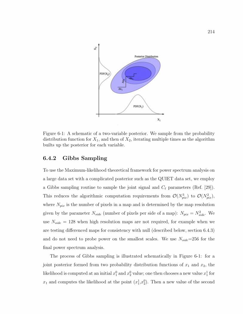
214
Figure 6-1: A schematic of a two-variable posterior. We sample from the probabilitydistribution function for X1, and then of X2, iterating multiple times as the algorithmbuilts up the posterior for each variable.
6.4.2 Gibbs Sampling
To use the Maximum-likelihood theoretical framework for power spectrum analysis on
a large data set with a complicated posterior such as the QUIET data set, we employ
a Gibbs sampling routine to sample the joint signal and C parameters (Ref. [29]).
This reduces the algorithmic computation requirements from O(N3
pix) to O(N2
pix),
where Npix is the number of pixels in a map and is determined by the map resolution
given by the parameter Nside (number of pixels per side of a map): Npix = N2
side. We
use Nside = 128 when high resolution maps are not required, for example when we
are testing differenced maps for consistency with null (described below, section 6.4.3)
and do not need to probe power on the smallest scales. We use Nside=256 for the
final power spectrum analysis.
The process of Gibbs sampling is illustrated schematically in Figure 6-1: for a
joint posterior formed from two probability distribution functions of x1 and x2, the
likelihood is computed at an initial x0
1and x
0
2value; one then chooses a new value x
1
1for
x1 and computes the likelihood at the point (x1
1,x0
2). Then a new value of the second
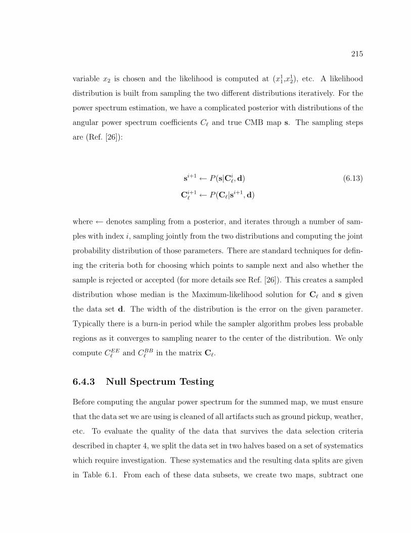
215
variable x2 is chosen and the likelihood is computed at (x1
1,x1
2), etc. A likelihood
distribution is built from sampling the two different distributions iteratively. For the
power spectrum estimation, we have a complicated posterior with distributions of the
angular power spectrum coefficients C and true CMB map s. The sampling steps
are (Ref. [26]):
si+1← P (s|Ci
,d) (6.13)
Ci+1
← P (C|si+1
,d)
where ← denotes sampling from a posterior, and iterates through a number of sam-
ples with index i, sampling jointly from the two distributions and computing the joint
probability distribution of those parameters. There are standard techniques for defin-
ing the criteria both for choosing which points to sample next and also whether the
sample is rejected or accepted (for more details see Ref. [26]). This creates a sampled
distribution whose median is the Maximum-likelihood solution for C and s given
the data set d. The width of the distribution is the error on the given parameter.
Typically there is a burn-in period while the sampler algorithm probes less probable
regions as it converges to sampling nearer to the center of the distribution. We only
compute CEE and C
BB in the matrix C.
6.4.3 Null Spectrum Testing
Before computing the angular power spectrum for the summed map, we must ensure
that the data set we are using is cleaned of all artifacts such as ground pickup, weather,
etc. To evaluate the quality of the data that survives the data selection criteria
described in chapter 4, we split the data set in two halves based on a set of systematics
which require investigation. These systematics and the resulting data splits are given
in Table 6.1. From each of these data subsets, we create two maps, subtract one
216
map from the other to produce a ‘difference map’, and compute the power spectrum
of the difference map using the same formalism used to create the angular power
spectrum of the data. For example, if we are concerned about ground contamination,
we can divide the data by the elevation of the sidelobe, as the maps with a low
sidelobe elevations would be expected to have greater ground contamination. The
signal should be removed in the difference map, leaving only noise, and the resulting
power spectrum should be consistent with null power. If there are coherent artifacts
which could bias the final result, they will appear as non-null bins in the power
spectrum, and indicate that the data selection criteria will need to be improved.
We run an extensive suite of null-tests, each designed to probe a different potential
systematic error, and we do not compute the data power spectrum until all null-tests
are consistent with null power.
The Maximum-likelihood power spectrum estimation algorithm is computation-
ally intensive, so we selected a suite of 22 null tests to test the most critical system-
atic effects. These tests are summarized in Table 6.1, and we evaluate them for six
angular-multipole bins: 25< <75, 75 < <125, 125 < <175, 175 < < 225,
225 < < 275, 275 < < 325 (with a higher Nside we will add an additional upper
bin).
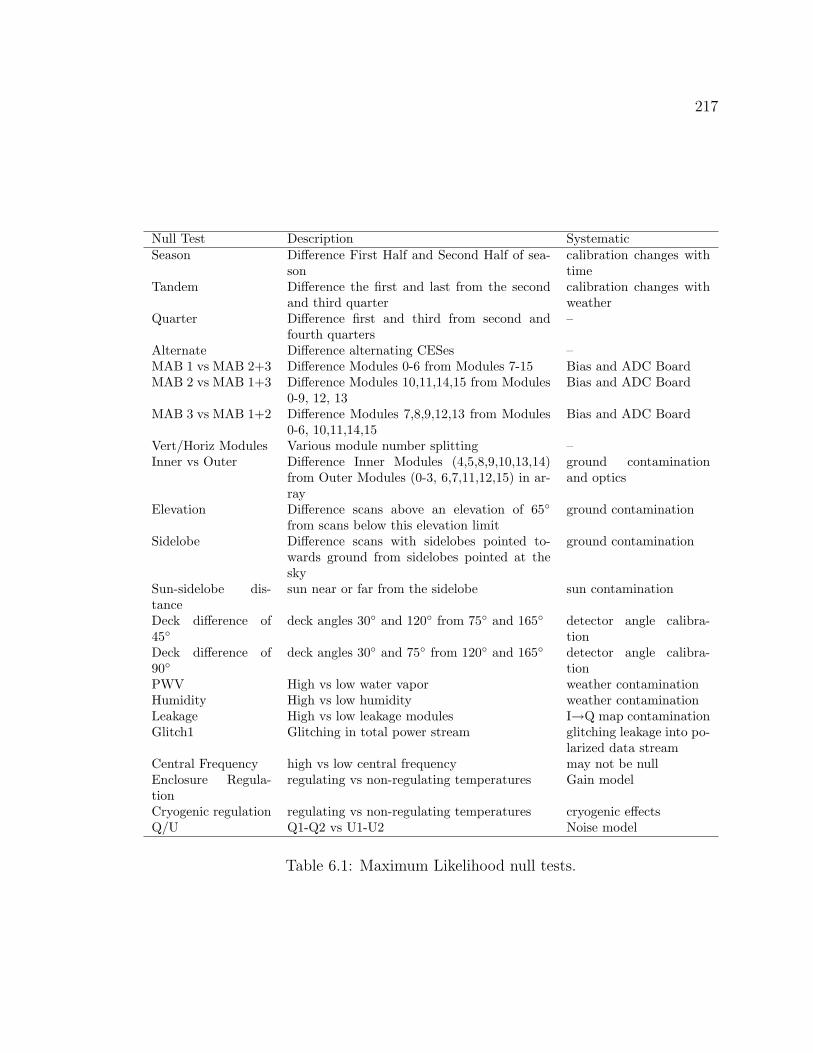
217
Null Test Description SystematicSeason Difference First Half and Second Half of sea-
soncalibration changes withtime
Tandem Difference the first and last from the secondand third quarter
calibration changes withweather
Quarter Difference first and third from second andfourth quarters
–
Alternate Difference alternating CESes –MAB 1 vs MAB 2+3 Difference Modules 0-6 from Modules 7-15 Bias and ADC BoardMAB 2 vs MAB 1+3 Difference Modules 10,11,14,15 from Modules
0-9, 12, 13Bias and ADC Board
MAB 3 vs MAB 1+2 Difference Modules 7,8,9,12,13 from Modules0-6, 10,11,14,15
Bias and ADC Board
Vert/Horiz Modules Various module number splitting –Inner vs Outer Difference Inner Modules (4,5,8,9,10,13,14)
from Outer Modules (0-3, 6,7,11,12,15) in ar-ray
ground contaminationand optics
Elevation Difference scans above an elevation of 65from scans below this elevation limit
ground contamination
Sidelobe Difference scans with sidelobes pointed to-wards ground from sidelobes pointed at thesky
ground contamination
Sun-sidelobe dis-tance
sun near or far from the sidelobe sun contamination
Deck difference of45
deck angles 30 and 120 from 75 and 165 detector angle calibra-tion
Deck difference of90
deck angles 30 and 75 from 120 and 165 detector angle calibra-tion
PWV High vs low water vapor weather contaminationHumidity High vs low humidity weather contaminationLeakage High vs low leakage modules I→Q map contaminationGlitch1 Glitching in total power stream glitching leakage into po-
larized data streamCentral Frequency high vs low central frequency may not be nullEnclosure Regula-tion
regulating vs non-regulating temperatures Gain model
Cryogenic regulation regulating vs non-regulating temperatures cryogenic effectsQ/U Q1-Q2 vs U1-U2 Noise model
Table 6.1: Maximum Likelihood null tests.
218
Prior to computing a null power spectrum, we can evaluate how likely a spectrum
is to be null based on the characteristics of the differenced map. We compute a
measure of our deviation from a signal-free, noise-dominated map as:
σmap =χ
2 − 1√
2N(6.14)
(6.15)
where
χ2 =
1
N
p
(dp −modelp)2
σ2p
(6.16)
and where dp is the value of the map at pixel p, N is the number of degrees of
freedom (Npix), and σp is the noise computed for the pth pixel from the noise model
(chapter 4). modelp gives a value for the pixel p from a data model; because we are
testing a null hypothesis, in this case modelp = 0. The χ2 is a reduced χ
2 such that
a value of 1 would indicate that the variance of the difference between the data and
the noise model consistent with the noise. We use the values of σmap as an internal
diagnostic to evaluate the properties of the differenced map, and hence how confident
we are to begin the computationally intensive step of computing the angular power
spectrum. Usually we choose a σmap within 3σ as acceptable to proceed to angular
power spectrum analysis.
Nullity Condition for the Power Spectrum
The Maximum-likelihood pipeline finds only non-negative solutions to the C spec-
trum. This will yield power spectra which are always positive, and yield a distribution
width which does not trivially show that a given C is consistent with zero. To quan-
tify the consistency with null power, we test the power spectrum against simulations
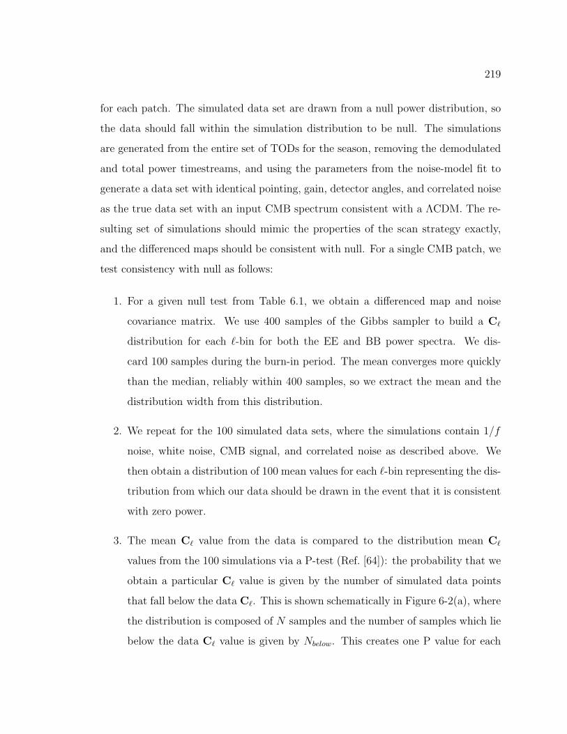
219
for each patch. The simulated data set are drawn from a null power distribution, so
the data should fall within the simulation distribution to be null. The simulations
are generated from the entire set of TODs for the season, removing the demodulated
and total power timestreams, and using the parameters from the noise-model fit to
generate a data set with identical pointing, gain, detector angles, and correlated noise
as the true data set with an input CMB spectrum consistent with a ΛCDM. The re-
sulting set of simulations should mimic the properties of the scan strategy exactly,
and the differenced maps should be consistent with null. For a single CMB patch, we
test consistency with null as follows:
1. For a given null test from Table 6.1, we obtain a differenced map and noise
covariance matrix. We use 400 samples of the Gibbs sampler to build a C
distribution for each -bin for both the EE and BB power spectra. We dis-
card 100 samples during the burn-in period. The mean converges more quickly
than the median, reliably within 400 samples, so we extract the mean and the
distribution width from this distribution.
2. We repeat for the 100 simulated data sets, where the simulations contain 1/f
noise, white noise, CMB signal, and correlated noise as described above. We
then obtain a distribution of 100 mean values for each -bin representing the dis-
tribution from which our data should be drawn in the event that it is consistent
with zero power.
3. The mean C value from the data is compared to the distribution mean C
values from the 100 simulations via a P-test (Ref. [64]): the probability that we
obtain a particular C value is given by the number of simulated data points
that fall below the data C. This is shown schematically in Figure 6-2(a), where
the distribution is composed of N samples and the number of samples which lie
below the data C value is given by Nbelow. This creates one P value for each
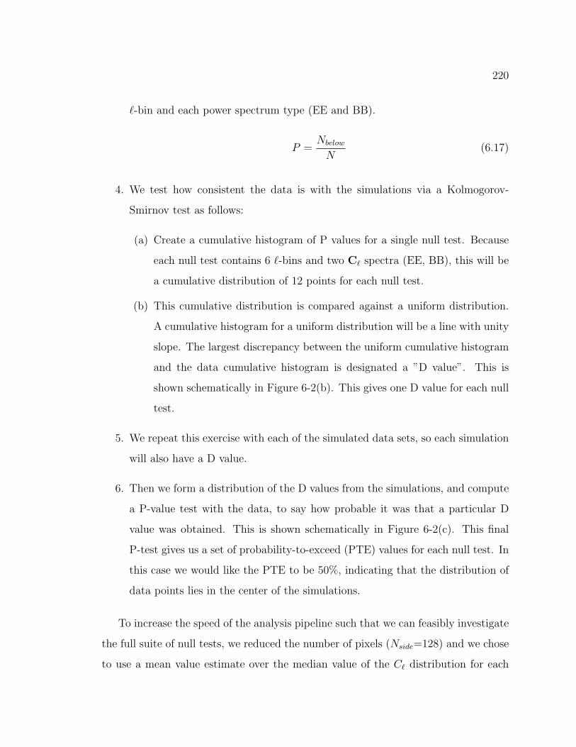
220
-bin and each power spectrum type (EE and BB).
P =Nbelow
N(6.17)
4. We test how consistent the data is with the simulations via a Kolmogorov-
Smirnov test as follows:
(a) Create a cumulative histogram of P values for a single null test. Because
each null test contains 6 -bins and two C spectra (EE, BB), this will be
a cumulative distribution of 12 points for each null test.
(b) This cumulative distribution is compared against a uniform distribution.
A cumulative histogram for a uniform distribution will be a line with unity
slope. The largest discrepancy between the uniform cumulative histogram
and the data cumulative histogram is designated a ”D value”. This is
shown schematically in Figure 6-2(b). This gives one D value for each null
test.
5. We repeat this exercise with each of the simulated data sets, so each simulation
will also have a D value.
6. Then we form a distribution of the D values from the simulations, and compute
a P-value test with the data, to say how probable it was that a particular D
value was obtained. This is shown schematically in Figure 6-2(c). This final
P-test gives us a set of probability-to-exceed (PTE) values for each null test. In
this case we would like the PTE to be 50%, indicating that the distribution of
data points lies in the center of the simulations.
To increase the speed of the analysis pipeline such that we can feasibly investigate
the full suite of null tests, we reduced the number of pixels (Nside=128) and we chose
to use a mean value estimate over the median value of the C distribution for each
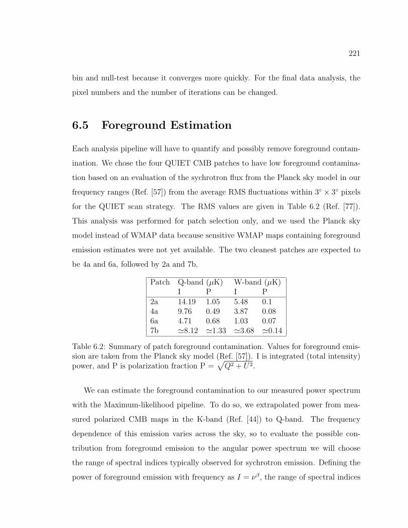
221
bin and null-test because it converges more quickly. For the final data analysis, the
pixel numbers and the number of iterations can be changed.
6.5 Foreground Estimation
Each analysis pipeline will have to quantify and possibly remove foreground contam-
ination. We chose the four QUIET CMB patches to have low foreground contamina-
tion based on an evaluation of the sychrotron flux from the Planck sky model in our
frequency ranges (Ref. [57]) from the average RMS fluctuations within 3 × 3 pixels
for the QUIET scan strategy. The RMS values are given in Table 6.2 (Ref. [77]).
This analysis was performed for patch selection only, and we used the Planck sky
model instead of WMAP data because sensitive WMAP maps containing foreground
emission estimates were not yet available. The two cleanest patches are expected to
be 4a and 6a, followed by 2a and 7b.
Patch Q-band (µK) W-band (µK)I P I P
2a 14.19 1.05 5.48 0.14a 9.76 0.49 3.87 0.086a 4.71 0.68 1.03 0.077b 8.12 1.33 3.68 0.14
Table 6.2: Summary of patch foreground contamination. Values for foreground emis-sion are taken from the Planck sky model (Ref. [57]). I is integrated (total intensity)power, and P is polarization fraction P =
Q2 + U2.
We can estimate the foreground contamination to our measured power spectrum
with the Maximum-likelihood pipeline. To do so, we extrapolated power from mea-
sured polarized CMB maps in the K-band (Ref. [44]) to Q-band. The frequency
dependence of this emission varies across the sky, so to evaluate the possible con-
tribution from foreground emission to the angular power spectrum we will choose
the range of spectral indices typically observed for sychrotron emission. Defining the
power of foreground emission with frequency as I = νβ, the range of spectral indices
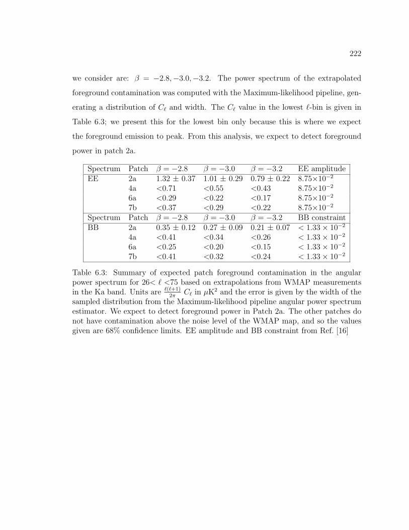
222
we consider are: β = −2.8,−3.0,−3.2. The power spectrum of the extrapolated
foreground contamination was computed with the Maximum-likelihood pipeline, gen-
erating a distribution of C and width. The C value in the lowest -bin is given in
Table 6.3; we present this for the lowest bin only because this is where we expect
the foreground emission to peak. From this analysis, we expect to detect foreground
power in patch 2a.
Spectrum Patch β = −2.8 β = −3.0 β = −3.2 EE amplitudeEE 2a 1.32 ± 0.37 1.01 ± 0.29 0.79 ± 0.22 8.75×10⁻²
4a <0.71 <0.55 <0.43 8.75×10⁻²
6a <0.29 <0.22 <0.17 8.75×10⁻²
7b <0.37 <0.29 <0.22 8.75×10⁻²
Spectrum Patch β = −2.8 β = −3.0 β = −3.2 BB constraintBB 2a 0.35 ± 0.12 0.27 ± 0.09 0.21 ± 0.07 < 1.33× 10⁻²
4a <0.41 <0.34 <0.26 < 1.33× 10⁻²
6a <0.25 <0.20 <0.15 < 1.33× 10⁻²
7b <0.41 <0.32 <0.24 < 1.33× 10⁻²
Table 6.3: Summary of expected patch foreground contamination in the angularpower spectrum for 26< <75 based on extrapolations from WMAP measurementsin the Ka band. Units are (+1)
2π C in µK2 and the error is given by the width of thesampled distribution from the Maximum-likelihood pipeline angular power spectrumestimator. We expect to detect foreground power in Patch 2a. The other patches donot have contamination above the noise level of the WMAP map, and so the valuesgiven are 68% confidence limits. EE amplitude and BB constraint from Ref. [16]
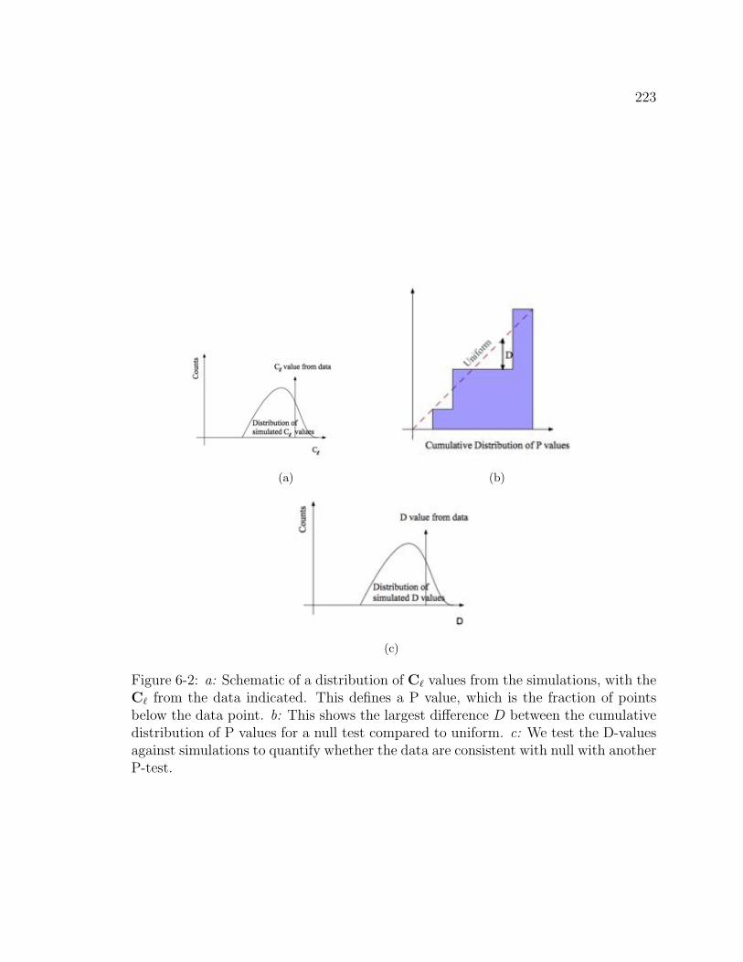
223
(a) (b)
(c)
Figure 6-2: a: Schematic of a distribution of C values from the simulations, with theC from the data indicated. This defines a P value, which is the fraction of pointsbelow the data point. b: This shows the largest difference D between the cumulativedistribution of P values for a null test compared to uniform. c: We test the D-valuesagainst simulations to quantify whether the data are consistent with null with anotherP-test.
224
6.6 Preliminary Results
6.6.1 Galactic Center
We compared polarization maps of the galactic center made from QUIET data with
maps made from WMAP data (Ref. [44]), shown in Figures 6-3(a) and 6-3(b). The
number of hours on the patch of sky is similar between the two maps, showing the
higher quality polarization data from QUIET.
6.6.2 Null Tests
We use the Maximum-Likelihood algorithm to compute the null-maps and null-power
spectra given in table 6.1. An example of a preliminary null map and power spectrum
for the ‘pointel’ null test (differencing data when the elevation of the sidelobes are
high from scans in which the sidelobes are at low elevations and possibly contami-
nated by emission from the ground) is given in Figures 6-4 and 6-5. As described in
section 6.4.3, the C value for each -bin (and for both the EE and BB spectra) is
tested against a distribution of simulations, and a P-value is obtained. A cumulative
histogram of these P-values for this null-test is given in Figure 6-6.
As discussed in section 6.4.3, each null-test will yield a probability to exceed. At
the time of this writing, these values are not yet computed with a reliable set of
simulations, we expect the results to appear in Ref. [18].
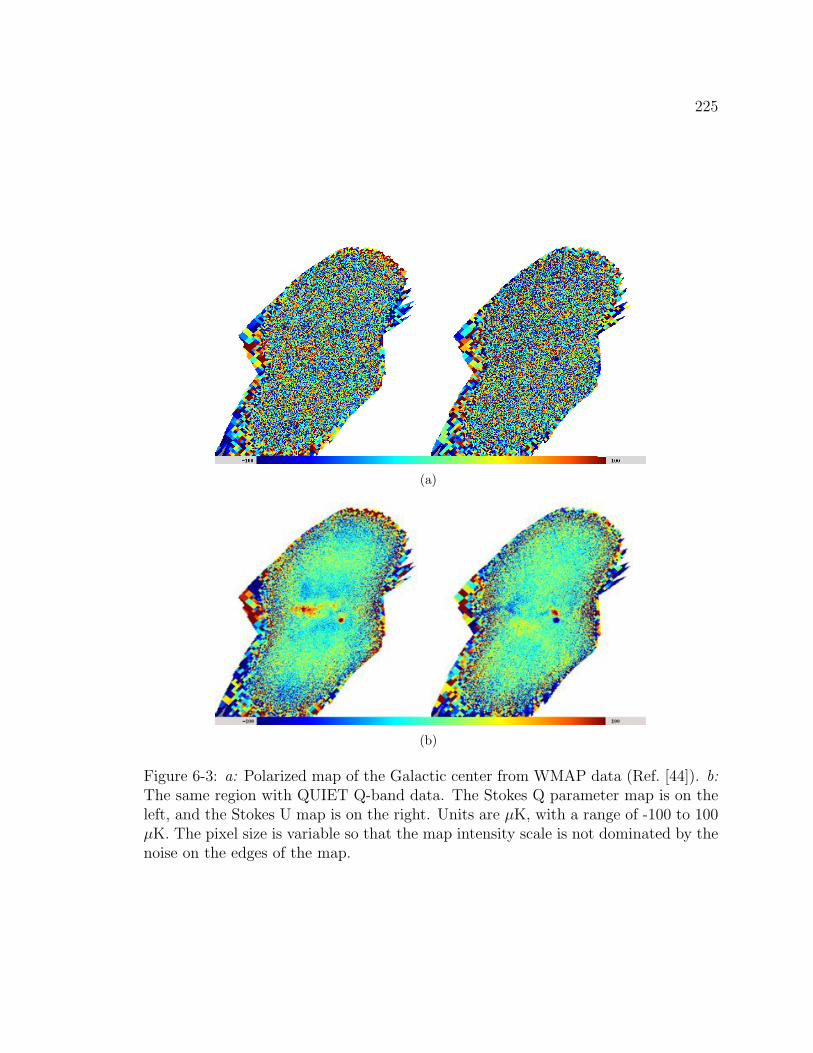
225
(a)
(b)
Figure 6-3: a: Polarized map of the Galactic center from WMAP data (Ref. [44]). b:
The same region with QUIET Q-band data. The Stokes Q parameter map is on theleft, and the Stokes U map is on the right. Units are µK, with a range of -100 to 100µK. The pixel size is variable so that the map intensity scale is not dominated by thenoise on the edges of the map.
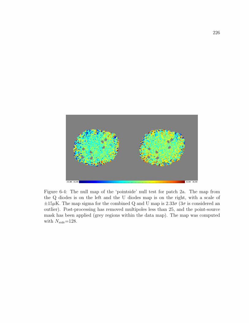
226
Figure 6-4: The null map of the ‘pointside’ null test for patch 2a. The map fromthe Q diodes is on the left and the U diodes map is on the right, with a scale of±15µK. The map sigma for the combined Q and U map is 2.33σ (3σ is considered anoutlier). Post-processing has removed multipoles less than 25, and the point-sourcemask has been applied (grey regions within the data map). The map was computedwith Nside=128.
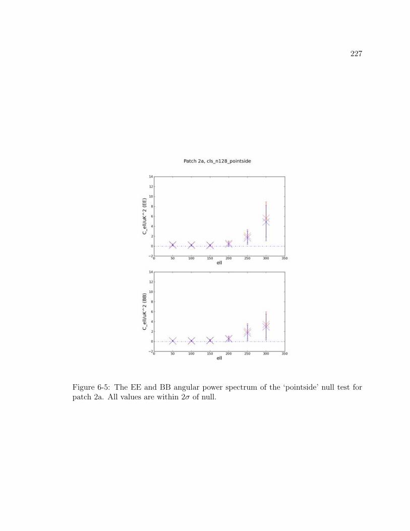
227
Figure 6-5: The EE and BB angular power spectrum of the ‘pointside’ null test forpatch 2a. All values are within 2σ of null.
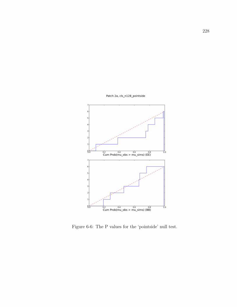
228
Figure 6-6: The P values for the ‘pointside’ null test.

Bibliography
[1] P. Bannister, G. Nixon, and S. Staggs. Final Preproduction Memo for QUIET
W-band OMTs. (internal memo), 2006.
[2] D. Barkats et al. CMB Polarimetry using Correlation Receivers with the PIQUE
and CAPMAP Experiments. 2005.
[3] D. Baumann and L. McAllister. A Microscopic Limit on Gravitational Waves
from D-brane Inflation. Phys. Rev. D, 75(12):123508–+, June 2007.
[4] Daniel Baumann et al. CMBPol Mission Concept Study: Probing Inflation with
CMB Polarization. AIP Conf. Proc., 1141:10–120, 2009.
[5] Dominic J. Benford, Michael C. Gaidis, and Jacob W. Kooi. Optical Properties
of Zitex in the Infrared to Submillimeter. Appl. Opt., 42(25):5118–5122, 2003.
[6] C. L. Bennett, R. S. Hill, G. Hinshaw, M. R. Nolta, N. Odegard, L. Page,
D. N. Spergel, J. L. Weiland, E. L. Wright, M. Halpern, N. Jarosik, A. Kogut,
M. Limon, S. S. Meyer, G. S. Tucker, and E. Wollack. First-Year Wilkinson Mi-
crowave Anisotropy Probe (WMAP) Observations: Foreground Emission. ApJS,
148:97–117, 2003.
[7] C. Bischoff, L. Hyatt, J. J. McMahon, G. W. Nixon, D. Samtleben, K. M. Smith,
K. Vanderlinde, D. Barkats, P. Farese, T. Gaier, J. O. Gundersen, M. M. Hed-
man, S. T. Staggs, and B. Winstein. New Measurements of Fine-Scale CMB
229
230
Polarization Power Spectra from CAPMAP at Both 40 and 90 GHz. ArXiv
e-prints, 802, February 2008.
[8] Colin Bischoff. Observing the Cosmic Microwave Background Polarization
Anisotropy at 40 GHz with QUIET. Ph.D. Thesis, August 2010.
[9] S. P. Boughn, D. M. Fram, and R. B. Partridge. Isotropy of the Microwave
Background at 8-millimeter Wavelength. ApJ, 165:439–+, May 1971.
[10] M. L. Brown, P. Ade, J. Bock, M. Bowden, G. Cahill, P. G. Castro, S. Church,
T. Culverhouse, R. B. Friedman, K. Ganga, W. K. Gear, S. Gupta, J. Hinderks,
J. Kovac, A. E. Lange, E. Leitch, S. J. Melhuish, Y. Memari, J. A. Murphy,
A. Orlando, C. O’Sullivan, L. Piccirillo, C. Pryke, N. Rajguru, B. Rusholme,
R. Schwarz, A. N. Taylor, K. L. Thompson, A. H. Turner, E. Y. S. Wu, M. Zem-
cov, and The QUa D collaboration. Improved Measurements of the Tempera-
ture and Polarization of the Cosmic Microwave Background from QUaD. ApJ,
705:978–999, November 2009.
[11] I. Buder. Type-B Glitch Correction. (internal memo), 2009.
[12] Immanuel Buder. Q/U Imaging Experiment (QUIET): a Ground-based Probe of
Cosmic Microwave Background Polarization. volume 7741, page 77411D. SPIE,
2010.
[13] S. Chang and Jr. Prata, A. A Design Procedure for Classical Offset Drago-
nian Antennas with Circular Apertures. In Antennas and Propagation Society
International Symposium, 1999. IEEE, volume 2, pages 1140 –1143 vol.2, aug
1999.
[14] Seunghyuk Chang and Jr. Prata, A. The Design of Classical Offset Dragonian
Reflector Antennas with Circular Apertures. Antennas and Propagation, IEEE
Transactions on, 52:12 – 19, 2004.
231
[15] Ming-Tang Chen, Yuh-Jing Hwang, West M. Ho, Homing Jiang, Tah-Hsuing
Chu, Li-Sien Wang, Sun-Nieng Hsieh, Johnson C. Han, and Malcolm M. Sin-
clair. Full-polarization W-band receiver for CMB detection. In Thomas G.
Phillips and Jonas Zmuidzinas, editors, Millimeter and Submillimeter Detectors
for Astronomy, volume 4855, pages 312–317. SPIE, 2003.
[16] H. C. Chiang, P. A. R. Ade, D. Barkats, J. O. Battle, E. M. Bierman, J. J.
Bock, C. D. Dowell, L. Duband, E. F. Hivon, W. L. Holzapfel, V. V. Hristov,
W. C. Jones, B. G. Keating, J. M. Kovac, C. L. Kuo, A. E. Lange, E. M.
Leitch, P. V. Mason, T. Matsumura, H. T. Nguyen, N. Ponthieu, C. Pryke,
S. Richter, G. Rocha, C. Sheehy, Y. D. Takahashi, J. E. Tolan, and K. W. Yoon.
Measurement of Cosmic Microwave Background Polarization Power Spectra from
Two Years of BICEP Data. ApJ, 711:1123–1140, March 2010.
[17] Yuji Chinone. Sun Side-lobe Cut. (internal memo), 2010.
[18] QUIET Collaboration. First Results from QUIET. (In preparation).
[19] QUIET Collaboration. First season QUIET results: Maximum Likelihood Anal-
ysis Methods. (In preparation).
[20] QUIET Collaboration. The QUIET Instrument. (In preparation).
[21] CTI-Cryogenics. Cryodyne Refrigeration System: Installation, Operation, and
Servicing Instructions. CTI Fridge manual, —.
[22] Clive Dickinson. Large Scale (1.4m) Beam Patterns. (internal memo), 2005.
[23] Scott Dodelson. Modern Cosmology. 2003. In press.
[24] Robert Dumoulin. (In preparation). Ph.D. Thesis, 2011.
[25] J. Dunkley, A. Amblard, C. Baccigalupi, M. Betoule, D. Chuss, A. Cooray, J. De-
labrouille, C. Dickinson, G. Dobler, J. Dotson, H. K. Eriksen, D. Finkbeiner,
232
D. Fixsen, P. Fosalba, A. Fraisse, C. Hirata, A. Kogut, J. Kristiansen,
C. Lawrence, A. M. Magalha˜Es, M. A. Miville-Deschenes, S. Meyer, A. Miller,
S. K. Naess, L. Page, H. V. Peiris, N. Phillips, E. Pierpaoli, G. Rocha, J. E.
Vaillancourt, and L. Verde. Prospects for polarized foreground removal. In
S. Dodelson, D. Baumann, A. Cooray, J. Dunkley, A. Fraisse, M. G. Jackson,
A. Kogut, L. Krauss, M. Zaldarriaga, & K. Smith , editor, American Institute of
Physics Conference Series, volume 1141 of American Institute of Physics Con-
ference Series, pages 222–264, June 2009.
[26] H. K. Eriksen, J. B. Jewell, C. Dickinson, A. J. Banday, K. M. Gorski, and C. R.
Lawrence. Joint Bayesian Component Separation and CMB Power Spectrum
Estimation. ArXiv e-prints, 709, September 2007.
[27] J. W. Fowler et al. THE Atacama Cosmology Telescope: A First Measurement of
the 600 < l < 8000 Cosmic Microwave Background Power Spectrum at 148GHz.
ArXiv e-prints, arXiv:1001.2934, January 2010.
[28] Todd Gaier. W-band Module Document. (internal memo).
[29] A. E. Gelfand and A. F. M. Smith. Jour. Amer. Statist. Assn, 85:398, 1990.
[30] B. Gold, N. Odegard, J. L. Weiland, R. S. Hill, A. Kogut, C. L. Bennett, G. Hin-
shaw, X. Chen, J. Dunkley, M. Halpern, N. Jarosik, E. Komatsu, D. Larson,
M. Limon, S. S. Meyer, M. R. Nolta, L. Page, K. M. Smith, D. N. Spergel,
G. S. Tucker, E. Wollack, and E. L. Wright. Seven-Year Wilkinson Microwave
Anisotropy Probe (WMAP) Observations: Galactic Foreground Emission. ArXiv
e-prints, January 2010.
[31] Paul. Goldsmith. Quasioptical Systems: Gaussian Beam Quasioptical Propataion
and Applications. IEEE Press, 1998.
[32] A. H. Guth. Inflationary universe: A Possible Solution to the Horizon and
Flatness Problems. Phys. Rev. D, 23:347, 1981.
233
[33] S. Hanany, P. Ade, A. Balbi, J. Bock, J. Borrill, A. Boscaleri, P. de Bernardis,
P. G. Ferreira, V. V. Hristov, A. H. Jaffe, A. E. Lange, A. T. Lee, P. D. Mauskopf,
C. B. Netterfield, S. Oh, E. Pascale, B. Rabii, P. L. Richards, G. F. Smoot,
R. Stompor, C. D. Winant, and J. H. P. Wu. MAXIMA-1: A Measurement of
the Cosmic Microwave Background Anisotropy on Angular Scales of 10’-5. ApJ,
545:L5–LL9, December 2000.
[34] Shaul Hanany and Philip Rosenkranz. Polarization of the Atmosphere as a
Foreground for Cosmic Microwave Background Polarization Experiments. New
Astronomy Reviews, 47(11-12):1159 – 1165, 2003. Proceedings of the Workshop
on The Cosmic Microwave Background Radiation and its Polarization.
[35] Eugene. Hecht. Optics, Fourth Edition. Addison-Wesley, 2002.
[36] G. Hinshaw, J. L. Weiland, R. S. Hill, N. Odegard, D. Larson, C. L. Ben-
nett, J. Dunkley, B. Gold, M. R. Greason, N. Jarosik, E. Komatsu, M. R.
Nolta, L. Page, D. N. Spergel, E. Wollack, M. Halpern, A. Kogut, M. Limon,
S. S. Meyer, G. S. Tucker, and E. L. Wright. Five-Year Wilkinson Microwave
Anisotropy Probe (WMAP) Observations: Data Processing, Sky Maps, and Ba-
sic Results. ApJS, 180:225–245, February 2009.
[37] C. M. Hirata, N. Padmanabhan, U. Seljak, D. Schlegel, and J. Brinkmann. Cross-
correlation of CMB with Large-Scale Structure: Weak Gravitational Lensing.
Phys. Rev. D, 70(10):103501–+, November 2004.
[38] E. Hivon, K. M. Gorski, C. B. Netterfield, B. P. Crill, S. Prunet, and F. Hansen.
MASTER of the Cosmic Microwave Background Anisotropy Power Spectrum: A
Fast Method for Statistical Analysis of Large and Complex Cosmic Microwave
Background Data Sets. ApJ, 567:2–17, March 2002.
[39] Christian Holler. Inner Ground Screen Simulations. (internal memo), 2007.
234
[40] Wayne Hu, Matthew M. Hedman, and Matias Zaldarriaga. Benchmark parame-
ters for CMB polarization experiments. Phys. Rev., D67:043004, 2003.
[41] Wayne Hu and Martin J. White. A CMB Polarization Primer. New Astron.,
2:323, 1997.
[42] W. Imbriale, C. Dickinson, and K. Thompson. QUIET: Large Scale (1.4m) W-
band Optical Design. (internal memo), 2005.
[43] John D. Jackson. Classical Electrodynamics. John Wiley and Son, Inc., 1999.
[44] N. Jarosik, C. L. Bennett, J. Dunkley, B. Gold, M. R. Greason, M. Halpern, R. S.
Hill, G. Hinshaw, A. Kogut, E. Komatsu, D. Larson, M. Limon, S. S. Meyer,
M. R. Nolta, N. Odegard, L. Page, K. M. Smith, D. N. Spergel, G. S. Tucker,
J. L. Weiland, E. Wollack, and E. L. Wright. Seven-Year Wilkinson Microwave
Anisotropy Probe (WMAP) Observations: Sky Maps, Systematic Errors, and
Basic Results. ArXiv e-prints, January 2010.
[45] N. Jarosik, C. L. Bennett, M. Halpern, G. Hinshaw, A. Kogut, M. Limon, S. S.
Meyer, L. Page, M. Pospieszalski, D. N. Spergel, G. S. Tucker, D. T. Wilkinson,
E. Wollack, E. L. Wright, and Z. Zhang. Design, Implementation, and Testing of
the Microwave Anisotropy Probe Radiometers. ApJS, 145:413–436, April 2003.
[46] W. C. Jones, P. A. R. Ade, J. J. Bock, J. R. Bond, J. Borrill, A. Boscaleri,
P. Cabella, C. R. Contaldi, B. P. Crill, P. de Bernardis, G. De Gasperis, A. de
Oliveira-Costa, G. De Troia, G. di Stefano, E. Hivon, A. H. Jaffe, T. S. Kisner,
A. E. Lange, C. J. MacTavish, S. Masi, P. D. Mauskopf, A. Melchiorri, T. E. Mon-
troy, P. Natoli, C. B. Netterfield, E. Pascale, F. Piacentini, D. Pogosyan, G. Po-
lenta, S. Prunet, S. Ricciardi, G. Romeo, J. E. Ruhl, P. Santini, M. Tegmark,
M. Veneziani, and N. Vittorio. A Measurement of the Angular Power Spectrum
of the CMB Temperature Anisotropy from the 2003 Flight of BOOMERANG.
ApJ, 647:823–832, August 2006.
235
[47] M. Kamionkowski, A. Kosowsky, and A. Stebbins. Statistics of Cosmic Mi-
crowave Background Polarization. Phys. Rev. D, 55:7368–7388, June 1997.
[48] P. Kangaslahti, T. Gaier, M. Seiffert, S. Weinreb, D. Harding, D. Dawson, M. So-
ria, C. Lawrence, B. Hooberman, and A. Miller. Planar Polarimetry Receivers
for Large Imaging Arrays at Q-band. In Microwave Symposium Digest, 2006.
IEEE MTT-S International, pages 89 –92, 11-16 2006.
[49] B Keating and E Wollack. Notes: Waveguide Hybrid Septum Polarizers. (internal
memo).
[50] Edward W. Kolb and Michael S. Turner. The Early Universe. Addison-Wesley,
New York, NY, 1990.
[51] E. Komatsu, K. M. Smith, J. Dunkley, C. L. Bennett, B. Gold, G. Hinshaw,
N. Jarosik, D. Larson, M. R. Nolta, L. Page, D. N. Spergel, M. Halpern, R. S.
Hill, A. Kogut, M. Limon, S. S. Meyer, N. Odegard, G. S. Tucker, J. L. Wei-
land, E. Wollack, and E. L. Wright. Seven-Year Wilkinson Microwave Anisotropy
Probe (WMAP) Observations: Cosmological Interpretation. ArXiv e-prints, Jan-
uary 2010.
[52] J. M. Kovac, E. M. Leitch, C. Pryke, J. E. Carlstrom, N. W. Halverson, and
W. L. Holzapfel. Detection of polarization in the cosmic microwave background
using DASI. Nature, 420:772–787, December 2002.
[53] John D. Kraus. Radio Astronomy. Cygnus-Quasar Books, 2004.
[54] J. Lamb. Miscellaneous Data on Material for Millimetre and Submillimetre Op-
tics. ALMA internal memo, —.
[55] D. L. Larson, H. K. Eriksen, B. D. Wandelt, K. M. Gorski, G. Huey, J. B. Jewell,
and I. J. O’Dwyer. Estimation of Polarized Power Spectra by Gibbs Sampling.
ApJ, 656:653–660, February 2007.
236
[56] C. R. Lawrence, T. C. Gaier, and M. Seiffert. Millimeter-wave MMIC cameras
and the QUIET experiment. In C. M. Bradford, P. A. R. Ade, J. E. Aguirre,
J. J. Bock, M. Dragovan, L. Duband, L. Earle, J. Glenn, H. Matsuhara, B. J. Nay-
lor, H. T. Nguyen, M. Yun, & J. Zmuidzinas, editor, Society of Photo-Optical
Instrumentation Engineers (SPIE) Conference Series, volume 5498 of Society of
Photo-Optical Instrumentation Engineers (SPIE) Conference Series, pages 220–
231, October 2004.
[57] S. M. Leach, J. . Cardoso, C. Baccigalupi, R. B. Barreiro, M. Betoule, J. Bobin,
A. Bonaldi, G. de Zotti, J. Delabrouille, C. Dickinson, H. K. Eriksen, J. Gonzalez-
Nuevo, F. K. Hansen, D. Herranz, M. LeJeune, M. Lopez-Caniego, E. Martinez-
Gonzalez, M. Massardi, J. . Melin, M. . Miville-Deschenes, G. Patanchon,
S. Prunet, S. Ricciardi, E. Salerno, J. L. Sanz, J. . Starck, F. Stivoli, V. Stol-
yarov, R. Stompor, and P. Vielva. Component Separation Methods for the Planck
Mission. ArXiv e-prints, May 2008.
[58] E. M. Leitch, J. M. Kovac, C. Pryke, J. E. Carlstrom, N. W. Halverson, W. L.
Holzapfel, M. Dragovan, B. Reddall, and E. S. Sandberg. Measurement of Po-
larization with the Degree Angular Scale Interferometer. Nature, 420:763–771,
December 2002.
[59] A. R. Liddle and D. H. Lyth. Cosmological Inflation and Large-Scale Structure.
Cambridge University Press, 2000.
[60] Andrew R. Liddle and David H. Lyth. COBE, Gravitational Waves, Inflation
and Extended Inflation. Phys. Lett., B291:391–398, 1992.
[61] Andrei D. Linde. A New Inflationary Universe Scenario: A Possible Solution of
the Horizon, Flatness, Homogeneity, Isotropy and Primordial Monopole Prob-
lems. Phys. Lett., B108:389–393, 1982.
237
[62] M. Lueker, C. L. Reichardt, K. K. Schaffer, O. Zahn, P. A. R. Ade, K. A. Aird,
B. A. Benson, L. E. Bleem, J. E. Carlstrom, C. L. Chang, H. M. Cho, T. M.
Crawford, A. T. Crites, T. de Haan, M. A. Dobbs, E. M. George, N. R. Hall,
N. W. Halverson, G. P. Holder, W. L. Holzapfel, J. D. Hrubes, M. Joy, R. Keisler,
L. Knox, A. T. Lee, E. M. Leitch, J. J. McMahon, J. Mehl, S. S. Meyer, J. J.
Mohr, T. E. Montroy, S. Padin, T. Plagge, C. Pryke, J. E. Ruhl, L. Shaw, E. Shi-
rokoff, H. G. Spieler, Z. Staniszewski, A. A. Stark, K. Vanderlinde, J. D. Vieira,
and R. Williamson. Measurements of Secondary Cosmic Microwave Background
Anisotropies with the South Pole Telescope. ArXiv e-prints, arXiv:0912.4317,
December 2009.
[63] Louis. Lyons. Statistics for Nuclear and Particle Physicists. Cambridge Univer-
sity Press, 1992.
[64] D. MacKay. Information Theory, Inference, and Learning Algorithms. Cam-
bridge University Press, 2003.
[65] J. C. Mather, E. S. Cheng, D. A. Cottingham, R. E. Eplee, D. J. Fixsen,
T. Hewagama, R. B. Isaacman, K. A. Jensen, S. S. Meyer, P. D. Noerdlinger,
S. M. Read, L. P. Rosen, R. A. Shafer, E. L. Wright, C. L. Bennett, N. W.
Boggess, M. G. Hauser, T. Kelsall, S. H. Moseley, R. F. Silverberg, G. F. Smoot,
R. Weiss, and D. T. Wilkinson. Measurement of the Cosmic Microwave Back-
ground Spectrum by the COBE FIRAS Instrument. ApJ, 420:439–444, January
1994.
[66] A. D. Miller et al. A Measurement of the Angular Power Spectrum of the CMB
from = 100 to 400. ApJ, 524:L1, 1999.
[67] Raul Monsalve. (In preparation). Ph.D. Thesis, 2012.
238
[68] Raul A. Monsalve. Beam characterization for the QUIET Q-Band Instrument us-
ing Polarized and Unpolarized Astronomical Sources. volume 7741, page 77412M.
SPIE, 2010.
[69] Glen Nixon. OMT Measurements. (internal memo), 2008.
[70] S. Padin, M. C. Shepherd, J. K. Cartwright, R. G. Keeney, B. S. Mason, T. J.
Pearson, A. C. S. Readhead, W. A. Schaal, J. Sievers, P. S. Udomprasert, J. K.
Yamasaki, W. L. Holzapfel, J. E. Carlstrom, M. Joy, S. T. Myers, and A. Otarola.
The Cosmic Background Imager. PASP, 114:83–97, January 2002.
[71] L. Page, C. Jackson, C. Barnes, C. Bennett, M. Halpern, G. Hinshaw, N. Jarosik,
A. Kogut, M. Limon, S. S. Meyer, D. N. Spergel, G. S. Tucker, D. T. Wilkinson,
E. Wollack, and E. L. Wright. The Optical Design and Characterization of the
Microwave Anisotropy Probe. ApJ, 585:566–586, March 2003.
[72] J. Pardo, J. Cernicharo, and E. Serabyn. Atmospheric Transmission at Mi-
crowaves (ATM): An Improved Model for Millimeter/Submillimeter Applica-
tions. In Transactions on Antennas and Propagation, 2001. IEEE, volume 49,
pages 1683–1694, dec 2001.
[73] David M.. Pozar. Microwave Engineering. Addison-Wesley Publishing Company,
Inc., 1993.
[74] C. Pryke, P. Ade, J. Bock, M. Bowden, M. L. Brown, G. Cahill, P. G. Castro,
S. Church, T. Culverhouse, R. Friedman, K. Ganga, W. K. Gear, S. Gupta,
J. Hinderks, J. Kovac, A. E. Lange, E. Leitch, S. J. Melhuish, Y. Memari, J. A.
Murphy, A. Orlando, R. Schwarz, C. O. Sullivan, L. Piccirillo, N. Rajguru,
B. Rusholme, A. N. Taylor, K. L. Thompson, A. H. Turner, E. Y. S. Wu, and
M. Zemcov. Second and Third Season QUaD Cosmic Microwave Background
Temperature and Polarization Power Spectra. ApJ, 692:1247–1270, February
2009.
239
[75] Britt Reichborn-Kjennerud. Building and Flying the E and B Experiment to
Measure the Polarization of the Cosmic Microwave Background. Ph.D. Thesis,
May 2010.
[76] J. Ruze. Antenna Tolerance Theory—A Review. Proc of the IEEE, 54:633–640,
1966.
[77] Dorothea Samtleben. Summary of Patch Selection. (internal memo), 2008.
[78] J. L. Sievers, C. Achermann, J. R. Bond, L. Bronfman, R. Bustos, C. R. Contaldi,
C. Dickinson, P. G. Ferreira, M. E. Jones, A. M. Lewis, B. S. Mason, J. May,
S. T. Myers, N. Oyarce, S. Padin, T. J. Pearson, M. Pospieszalski, A. C. S.
Readhead, R. Reeves, A. C. Taylor, and S. Torres. Implications of the Cosmic
Background Imager Polarization Data. ApJ, 660:976–987, May 2007.
[79] J. L. Sievers, B. S. Mason, L. Weintraub, C. Achermann, P. Altamirano, J. R.
Bond, L. Bronfman, R. Bustos, C. Contaldi, C. Dickinson, M. E. Jones, J. May,
S. T. Myers, N. Oyarce, S. Padin, T. J. Pearson, M. Pospieszalski, A. C. S.
Readhead, R. Reeves, M. C. Shepherd, A. C. Taylor, and S. Torres. Cosmolog-
ical Results from Five Years of 30 GHz CMB Intensity Measurements with the
Cosmic Background Imager. ArXiv e-prints, January 2009.
[80] D.S. Sivia. Data Analysis: A Bayesian Tutorial (2nd Ed.). Oxford University
Press, 2006.
[81] Kendrick M. Smith et al. CMBPol Mission Concept Study: Gravitational Lens-
ing. 2008.
[82] Kendrick M. Smith and Matias Zaldarriaga. A General Solution to the E-B
Mixing Problem. Phys. Rev., D76:043001, 2007.
[83] O. Tajima. Type-B Glitch Correction. (internal memo), 2009.
240
[84] Osamu Tajima. Systematic Error Estimation about Deck-Encoder Slip. (internal
memo), 2010.
[85] Osamu Tajima, Colin Bischoff, and Yuji Chinone. Q-band Detector Angle Sum-
mary and Systematic Error. (internal memo), 2010.
[86] M. Tegmark. How to Make Maps from Cosmic Microwave Background Data
Without Losing Information. ApJ, 480:87–90, May 1997.
[87] M. Tristram, G. Patanchon, J. F. Macıas-Perez, P. Ade, A. Amblard, R. Ansari,
E. Aubourg, A. Benoıt, J.-P. Bernard, A. Blanchard, J. J. Bock, F. R. Bouchet,
A. Bourrachot, P. Camus, J.-F. Cardoso, F. Couchot, P. de Bernardis, J. De-
labrouille, F.-X. Desert, M. Douspis, L. Dumoulin, P. Filliatre, P. Fosalba, M. Gi-
ard, Y. Giraud-Heraud, R. Gispert, L. Guglielmi, J.-C. Hamilton, S. Hanany,
S. Henrot-Versille, J. Kaplan, G. Lagache, J.-M. Lamarre, A. E. Lange, K. Madet,
B. Maffei, C. Magneville, S. Masi, F. Mayet, F. Nati, O. Perdereau, S. Plaszczyn-
ski, M. Piat, N. Ponthieu, S. Prunet, C. Renault, C. Rosset, D. Santos, D. Vibert,
and D. Yvon. The CMB Temperature Power Spectrum from an Improved Anal-
ysis of the Archeops Data. A&A, 436:785–797, June 2005.
[88] Department of Physics University of Miami. Q-Band Central Horn Beam Anal-
ysis using Tau A. (internal memo), 2010.
[89] B. D. Wandelt, D. L. Larson, and A. Lakshminarayanan. Global, Exact Cosmic
Microwave Background Data Analysis Using Gibbs Sampling. Phys. Rev. D,
70(8):083511–+, October 2004.
[90] J. L. Weiland, N. Odegard, R. S. Hill, E. Wollack, G. Hinshaw, M. R. Grea-
son, N. Jarosik, L. Page, C. L. Bennett, J. Dunkley, B. Gold, M. Halpern,
A. Kogut, E. Komatsu, D. Larson, M. Limon, S. S. Meyer, M. R. Nolta, K. M.
Smith, D. N. Spergel, G. S. Tucker, and E. L. Wright. Seven-Year Wilkinson
241
Microwave Anisotropy Probe (WMAP) Observations: Planets and Celestial Cal-
ibration Sources. ArXiv e-prints, January 2010.
[91] E. L. Wright, X. Chen, N. Odegard, C. L. Bennett, R. S. Hill, G. Hinshaw,
N. Jarosik, E. Komatsu, M. R. Nolta, L. Page, D. N. Spergel, J. L. Weiland,
E. Wollack, J. Dunkley, B. Gold, M. Halpern, A. Kogut, D. Larson, M. Limon,
S. S. Meyer, and G. S. Tucker. Five-Year Wilkinson Microwave Anisotropy Probe
(WMAP) Observations: Source Catalog. ApJS, 180:283–295, February 2009.
[92] M. Zaldarriaga and U. Seljak. All-sky Analysis of Polarization in the Microwave
Background. Phys. Rev. D, 55:1830–1840, February 1997.
[93] Matias Zaldarriaga and Uros Seljak. Gravitational Lensing Effect on Cosmic
Microwave Background Polarization. Phys. Rev., D58:023003, 1998.
Appendix A
Module Signal Processing
A.1 Phase Switch Transmission Imbalance
Here we consider the action of phase switching both legs, and include the possibility
that the transmission coefficient in one phase switch state is not identical to the
transmission coefficient in the other state. The results are presented in section 2.3.5,
the following is a derivation of those results. The phase switching Jones matrix we
consider will be:
eiφA 0
0 eiφB
→
+1
−βA0
0 +1
−βB
(A.1)
Before, we considered eiφA = 1 and e
iφB = ±1. With this new expression for the
phase switching matrix, we have added the following elements:
• We can phase-switch both legs, such that eiφA has two possible states, and
similarly for eiφB .
• The two phase switch states for each phase switch can have unequal transmission
coefficients. Here we assume the transmission is normalized such that in one
242
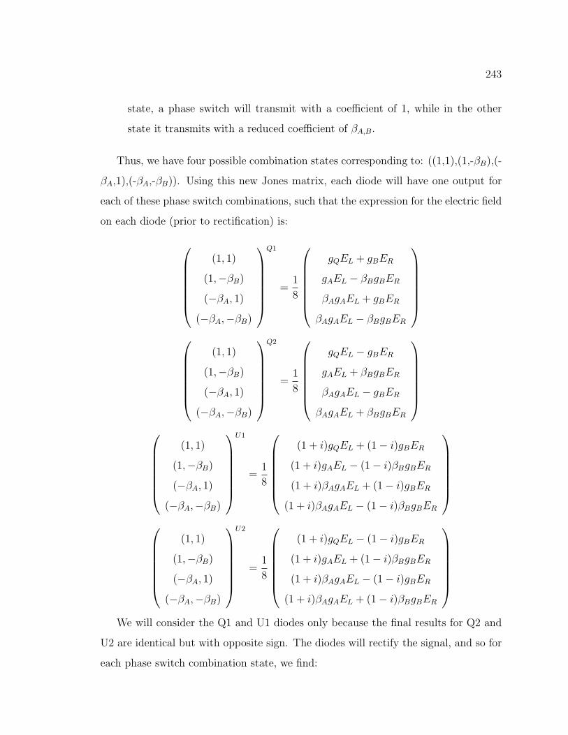
243
state, a phase switch will transmit with a coefficient of 1, while in the other
state it transmits with a reduced coefficient of βA,B.
Thus, we have four possible combination states corresponding to: ((1,1),(1,-βB),(-
βA,1),(-βA,-βB)). Using this new Jones matrix, each diode will have one output for
each of these phase switch combinations, such that the expression for the electric field
on each diode (prior to rectification) is:
(1, 1)
(1,−βB)
(−βA, 1)
(−βA,−βB)
Q1
=1
8
gQEL + gBER
gAEL − βBgBER
βAgAEL + gBER
βAgAEL − βBgBER
(1, 1)
(1,−βB)
(−βA, 1)
(−βA,−βB)
Q2
=1
8
gQEL − gBER
gAEL + βBgBER
βAgAEL − gBER
βAgAEL + βBgBER
(1, 1)
(1,−βB)
(−βA, 1)
(−βA,−βB)
U1
=1
8
(1 + i)gQEL + (1− i)gBER
(1 + i)gAEL − (1− i)βBgBER
(1 + i)βAgAEL + (1− i)gBER
(1 + i)βAgAEL − (1− i)βBgBER
(1, 1)
(1,−βB)
(−βA, 1)
(−βA,−βB)
U2
=1
8
(1 + i)gQEL − (1− i)gBER
(1 + i)gAEL + (1− i)βBgBER
(1 + i)βAgAEL − (1− i)gBER
(1 + i)βAgAEL + (1− i)βBgBER
We will consider the Q1 and U1 diodes only because the final results for Q2 and
U2 are identical but with opposite sign. The diodes will rectify the signal, and so for
each phase switch combination state, we find:
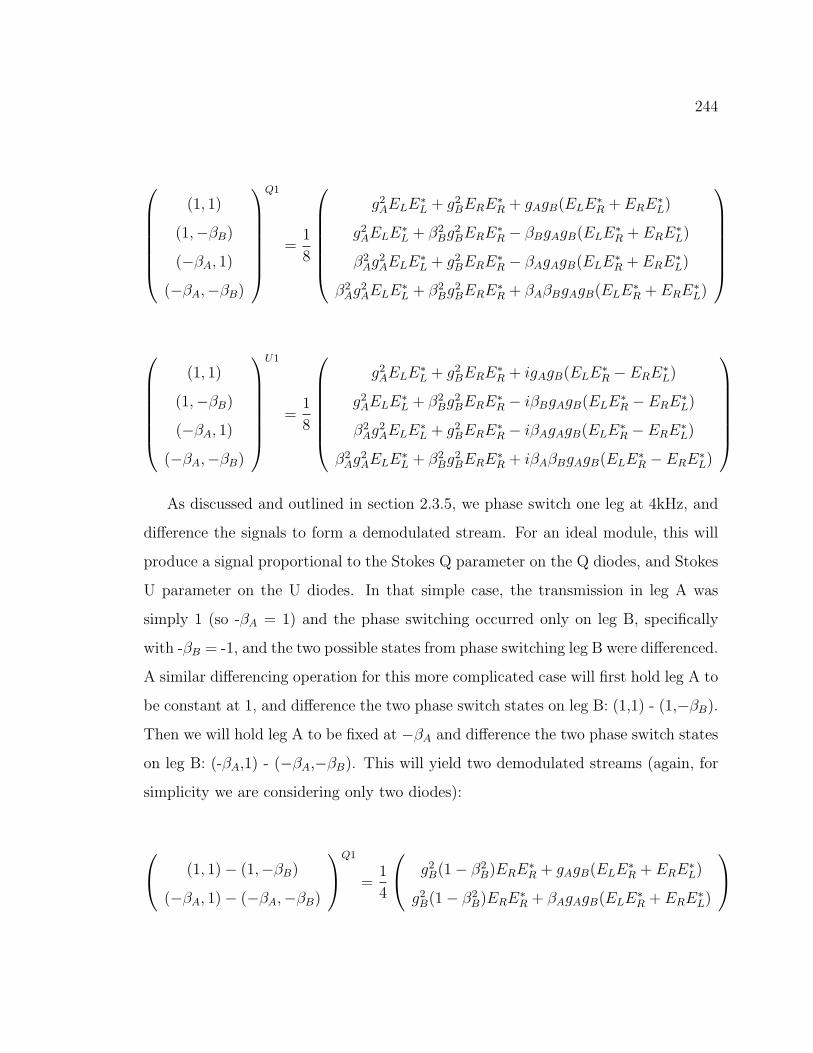
244
(1, 1)
(1,−βB)
(−βA, 1)
(−βA,−βB)
Q1
=1
8
g2
AELE∗L + g
2
BERE∗R + gAgB(ELE
∗R + ERE
∗L)
g2
AELE∗L + β
2
Bg2
BERE∗R − βBgAgB(ELE
∗R + ERE
∗L)
β2
Ag2
AELE∗L + g
2
BERE∗R − βAgAgB(ELE
∗R + ERE
∗L)
β2
Ag2
AELE∗L + β
2
Bg2
BERE∗R + βAβBgAgB(ELE
∗R + ERE
∗L)
(1, 1)
(1,−βB)
(−βA, 1)
(−βA,−βB)
U1
=1
8
g2
AELE∗L + g
2
BERE∗R + igAgB(ELE
∗R − ERE
∗L)
g2
AELE∗L + β
2
Bg2
BERE∗R − iβBgAgB(ELE
∗R − ERE
∗L)
β2
Ag2
AELE∗L + g
2
BERE∗R − iβAgAgB(ELE
∗R − ERE
∗L)
β2
Ag2
AELE∗L + β
2
Bg2
BERE∗R + iβAβBgAgB(ELE
∗R − ERE
∗L)
As discussed and outlined in section 2.3.5, we phase switch one leg at 4kHz, and
difference the signals to form a demodulated stream. For an ideal module, this will
produce a signal proportional to the Stokes Q parameter on the Q diodes, and Stokes
U parameter on the U diodes. In that simple case, the transmission in leg A was
simply 1 (so -βA = 1) and the phase switching occurred only on leg B, specifically
with -βB = -1, and the two possible states from phase switching leg B were differenced.
A similar differencing operation for this more complicated case will first hold leg A to
be constant at 1, and difference the two phase switch states on leg B: (1,1) - (1,−βB).
Then we will hold leg A to be fixed at −βA and difference the two phase switch states
on leg B: (-βA,1) - (−βA,−βB). This will yield two demodulated streams (again, for
simplicity we are considering only two diodes):
(1, 1)− (1,−βB)
(−βA, 1)− (−βA,−βB)
Q1
=1
4
g2
B(1− β2
B)ERE∗R + gAgB(ELE
∗R + ERE
∗L)
g2
B(1− β2
B)ERE∗R + βAgAgB(ELE
∗R + ERE
∗L)
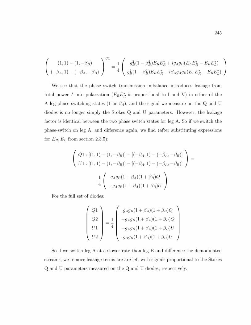
245
(1, 1)− (1,−βB)
(−βA, 1)− (−βA,−βB)
U1
=1
4
g2
B(1− β2
B)ERE∗R + igAgB(ELE
∗R − ERE
∗L)
g2
B(1− β2
B)ERE∗R − iβAgAgB(ELE
∗R − ERE
∗L)
We see that the phase switch transmission imbalance introduces leakage from
total power I into polarzation (ERE∗R is proportional to I and V) in either of the
A leg phase switching states (1 or βA), and the signal we measure on the Q and U
diodes is no longer simply the Stokes Q and U parameters. However, the leakage
factor is identical between the two phase switch states for leg A. So if we switch the
phase-switch on leg A, and difference again, we find (after substituting expressions
for ER, EL from section 2.3.5):
Q1 : [(1, 1)− (1,−βB)]− [(−βA, 1)− (−βA,−βB)]
U1 : [(1, 1)− (1,−βB)]− [(−βA, 1)− (−βA,−βB)]
=
1
4
gAgB(1 + βA)(1 + βB)Q
−gAgB(1 + βA)(1 + βB)U
For the full set of diodes:
Q1
Q2
U1
U2
=
1
4
gAgB(1 + βA)(1 + βB)Q
−gAgB(1 + βA)(1 + βB)Q
−gAgB(1 + βA)(1 + βB)U
gAgB(1 + βA)(1 + βB)U
So if we switch leg A at a slower rate than leg B and difference the demodulated
streams, we remove leakage terms are are left with signals proportional to the Stokes
Q and U parameters measured on the Q and U diodes, respectively.
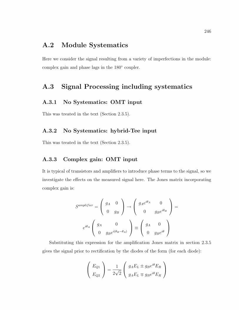
246
A.2 Module Systematics
Here we consider the signal resulting from a variety of imperfections in the module:
complex gain and phase lags in the 180 coupler.
A.3 Signal Processing including systematics
A.3.1 No Systematics: OMT input
This was treated in the text (Section 2.3.5).
A.3.2 No Systematics: hybrid-Tee input
This was treated in the text (Section 2.3.5).
A.3.3 Complex gain: OMT input
It is typical of transistors and amplifiers to introduce phase terms to the signal, so we
investigate the effects on the measured signal here. The Jones matrix incorporating
complex gain is:
Samplifier =
gA 0
0 gB
→
gAeiθA 0
0 gBeiθB
=
eiθA
gA 0
0 gBei(θB−θA)
≡
gA 0
0 gBeiθ
Substituting this expression for the amplification Jones matrix in section 2.3.5
gives the signal prior to rectification by the diodes of the form (for each diode):
EQ1
EQ2
=1
2√
2
gAEL ± gBeiθER
gAEL ∓ gBeiθER
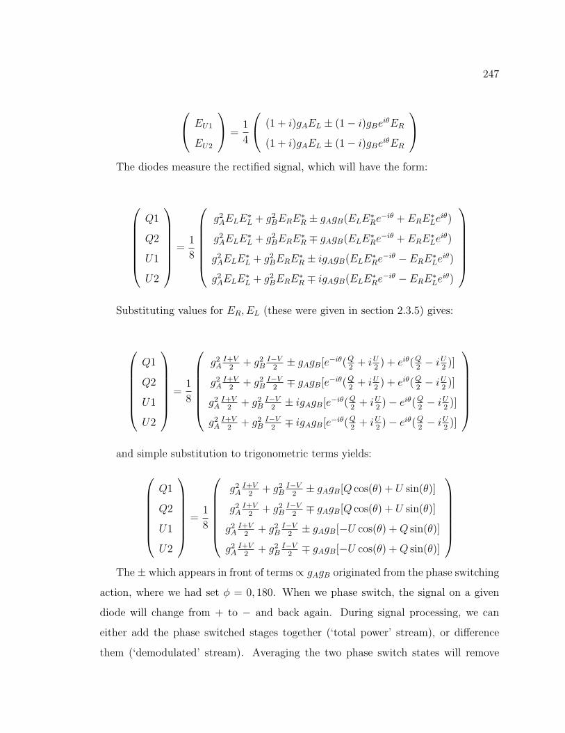
247
EU1
EU2
=1
4
(1 + i)gAEL ± (1− i)gBeiθER
(1 + i)gAEL ± (1− i)gBeiθER
The diodes measure the rectified signal, which will have the form:
Q1
Q2
U1
U2
=
1
8
g2
AELE∗L + g
2
BERE∗R ± gAgB(ELE
∗Re
−iθ + ERE∗Le
iθ)
g2
AELE∗L + g
2
BERE∗R ∓ gAgB(ELE
∗Re
−iθ + ERE∗Le
iθ)
g2
AELE∗L + g
2
BERE∗R ± igAgB(ELE
∗Re
−iθ − ERE∗Le
iθ)
g2
AELE∗L + g
2
BERE∗R ∓ igAgB(ELE
∗Re
−iθ − ERE∗Le
iθ)
Substituting values for ER, EL (these were given in section 2.3.5) gives:
Q1
Q2
U1
U2
=
1
8
g2
AI+V
2+ g
2
BI−V
2± gAgB[e−iθ(Q
2+ i
U2) + e
iθ(Q2− i
U2)]
g2
AI+V
2+ g
2
BI−V
2∓ gAgB[e−iθ(Q
2+ i
U2) + e
iθ(Q2− i
U2)]
g2
AI+V
2+ g
2
BI−V
2± igAgB[e−iθ(Q
2+ i
U2)− e
iθ(Q2− i
U2)]
g2
AI+V
2+ g
2
BI−V
2∓ igAgB[e−iθ(Q
2+ i
U2)− e
iθ(Q2− i
U2)]
and simple substitution to trigonometric terms yields:
Q1
Q2
U1
U2
=
1
8
g2
AI+V
2+ g
2
BI−V
2± gAgB[Q cos(θ) + U sin(θ)]
g2
AI+V
2+ g
2
BI−V
2∓ gAgB[Q cos(θ) + U sin(θ)]
g2
AI+V
2+ g
2
BI−V
2± gAgB[−U cos(θ) + Q sin(θ)]
g2
AI+V
2+ g
2
BI−V
2∓ gAgB[−U cos(θ) + Q sin(θ)]
The ± which appears in front of terms ∝ gAgB originated from the phase switching
action, where we had set φ = 0, 180. When we phase switch, the signal on a given
diode will change from + to − and back again. During signal processing, we can
either add the phase switched stages together (‘total power’ stream), or difference
them (‘demodulated’ stream). Averaging the two phase switch states will remove
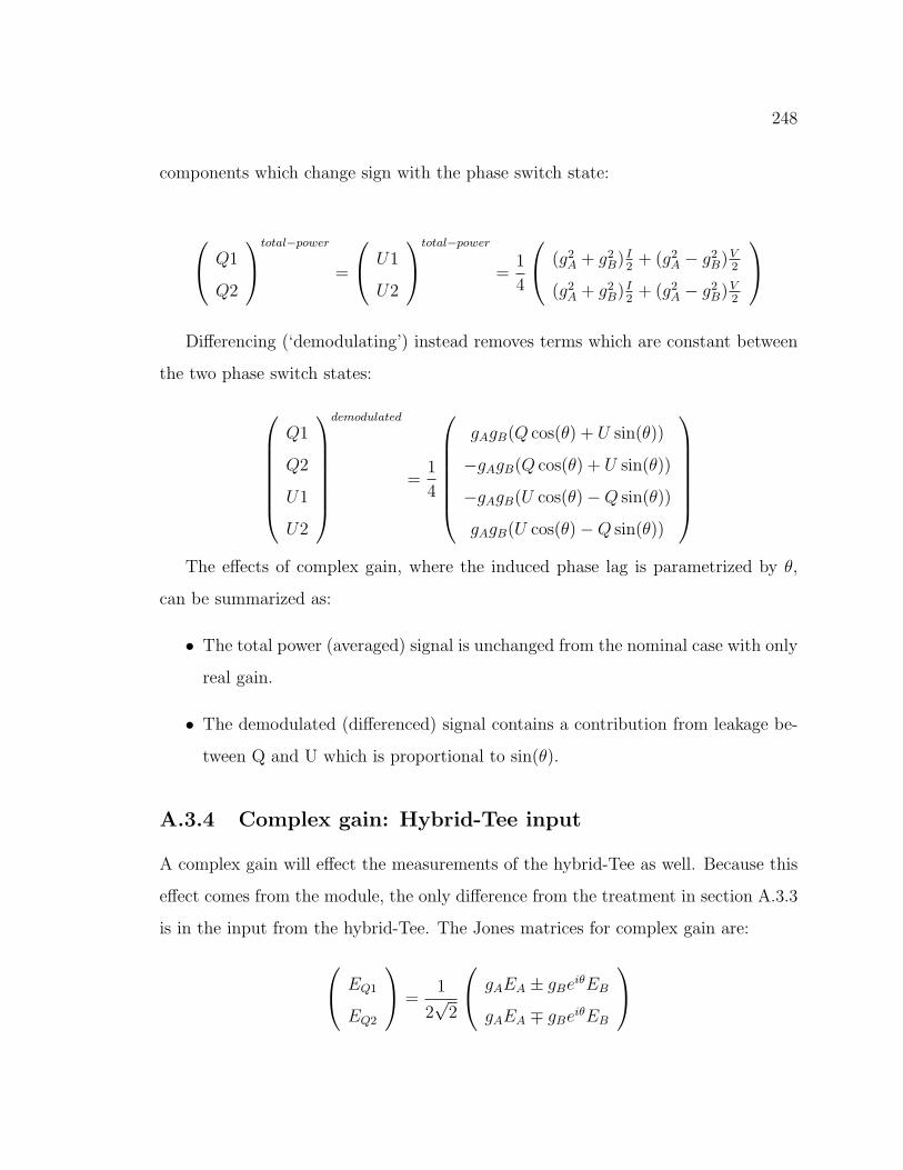
248
components which change sign with the phase switch state:
Q1
Q2
total−power
=
U1
U2
total−power
=1
4
(g2
A + g2
B) I2
+ (g2
A − g2
B)V2
(g2
A + g2
B) I2
+ (g2
A − g2
B)V2
Differencing (‘demodulating’) instead removes terms which are constant between
the two phase switch states:
Q1
Q2
U1
U2
demodulated
=1
4
gAgB(Q cos(θ) + U sin(θ))
−gAgB(Q cos(θ) + U sin(θ))
−gAgB(U cos(θ)−Q sin(θ))
gAgB(U cos(θ)−Q sin(θ))
The effects of complex gain, where the induced phase lag is parametrized by θ,
can be summarized as:
• The total power (averaged) signal is unchanged from the nominal case with only
real gain.
• The demodulated (differenced) signal contains a contribution from leakage be-
tween Q and U which is proportional to sin(θ).
A.3.4 Complex gain: Hybrid-Tee input
A complex gain will effect the measurements of the hybrid-Tee as well. Because this
effect comes from the module, the only difference from the treatment in section A.3.3
is in the input from the hybrid-Tee. The Jones matrices for complex gain are:
EQ1
EQ2
=1
2√
2
gAEA ± gBeiθEB
gAEA ∓ gBeiθEB
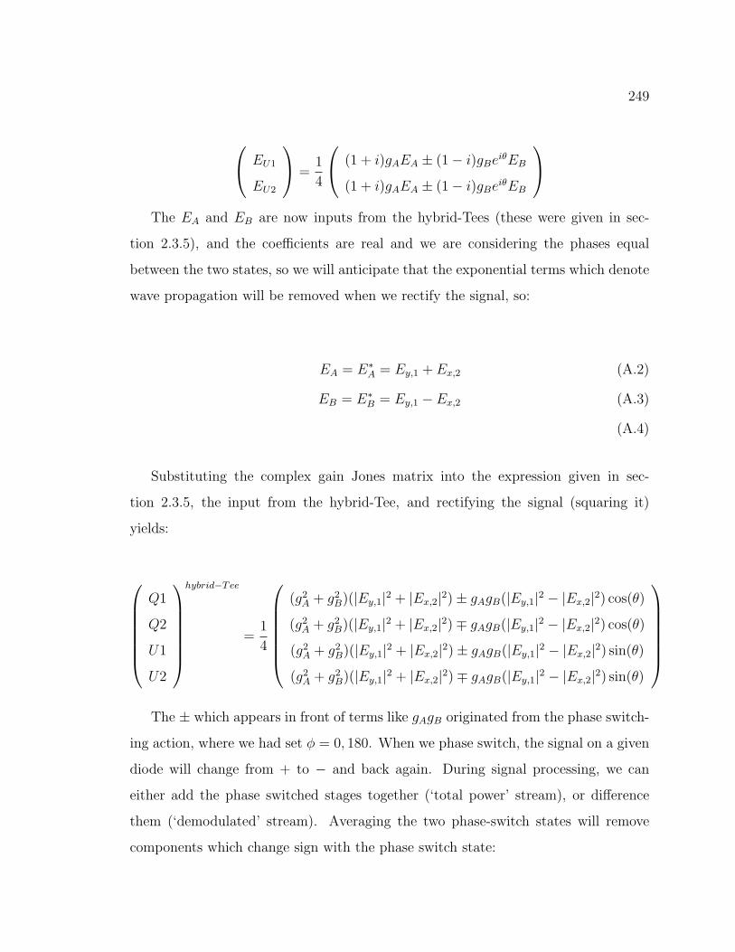
249
EU1
EU2
=1
4
(1 + i)gAEA ± (1− i)gBeiθEB
(1 + i)gAEA ± (1− i)gBeiθEB
The EA and EB are now inputs from the hybrid-Tees (these were given in sec-
tion 2.3.5), and the coefficients are real and we are considering the phases equal
between the two states, so we will anticipate that the exponential terms which denote
wave propagation will be removed when we rectify the signal, so:
EA = E∗A = Ey,1 + Ex,2 (A.2)
EB = E∗B = Ey,1 − Ex,2 (A.3)
(A.4)
Substituting the complex gain Jones matrix into the expression given in sec-
tion 2.3.5, the input from the hybrid-Tee, and rectifying the signal (squaring it)
yields:
Q1
Q2
U1
U2
hybrid−Tee
=1
4
(g2
A + g2
B)(|Ey,1|2 + |Ex,2|
2) ± gAgB(|Ey,1|2 − |Ex,2|
2) cos(θ)
(g2
A + g2
B)(|Ey,1|2 + |Ex,2|
2)∓ gAgB(|Ey,1|2 − |Ex,2|
2) cos(θ)
(g2
A + g2
B)(|Ey,1|2 + |Ex,2|
2) ± gAgB(|Ey,1|2 − |Ex,2|
2) sin(θ)
(g2
A + g2
B)(|Ey,1|2 + |Ex,2|
2)∓ gAgB(|Ey,1|2 − |Ex,2|
2) sin(θ)
The ± which appears in front of terms like gAgB originated from the phase switch-
ing action, where we had set φ = 0, 180. When we phase switch, the signal on a given
diode will change from + to − and back again. During signal processing, we can
either add the phase switched stages together (‘total power’ stream), or difference
them (‘demodulated’ stream). Averaging the two phase-switch states will remove
components which change sign with the phase switch state:
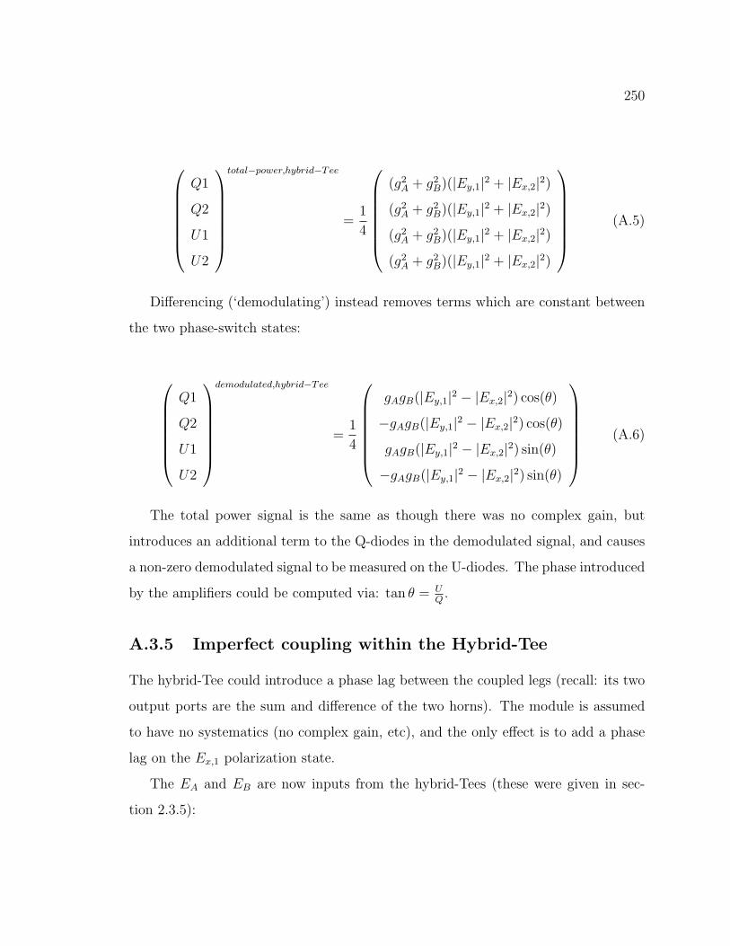
250
Q1
Q2
U1
U2
total−power,hybrid−Tee
=1
4
(g2
A + g2
B)(|Ey,1|2 + |Ex,2|
2)
(g2
A + g2
B)(|Ey,1|2 + |Ex,2|
2)
(g2
A + g2
B)(|Ey,1|2 + |Ex,2|
2)
(g2
A + g2
B)(|Ey,1|2 + |Ex,2|
2)
(A.5)
Differencing (‘demodulating’) instead removes terms which are constant between
the two phase-switch states:
Q1
Q2
U1
U2
demodulated,hybrid−Tee
=1
4
gAgB(|Ey,1|2 − |Ex,2|
2) cos(θ)
−gAgB(|Ey,1|2 − |Ex,2|
2) cos(θ)
gAgB(|Ey,1|2 − |Ex,2|
2) sin(θ)
−gAgB(|Ey,1|2 − |Ex,2|
2) sin(θ)
(A.6)
The total power signal is the same as though there was no complex gain, but
introduces an additional term to the Q-diodes in the demodulated signal, and causes
a non-zero demodulated signal to be measured on the U-diodes. The phase introduced
by the amplifiers could be computed via: tan θ = UQ .
A.3.5 Imperfect coupling within the Hybrid-Tee
The hybrid-Tee could introduce a phase lag between the coupled legs (recall: its two
output ports are the sum and difference of the two horns). The module is assumed
to have no systematics (no complex gain, etc), and the only effect is to add a phase
lag on the Ex,1 polarization state.
The EA and EB are now inputs from the hybrid-Tees (these were given in sec-
tion 2.3.5):
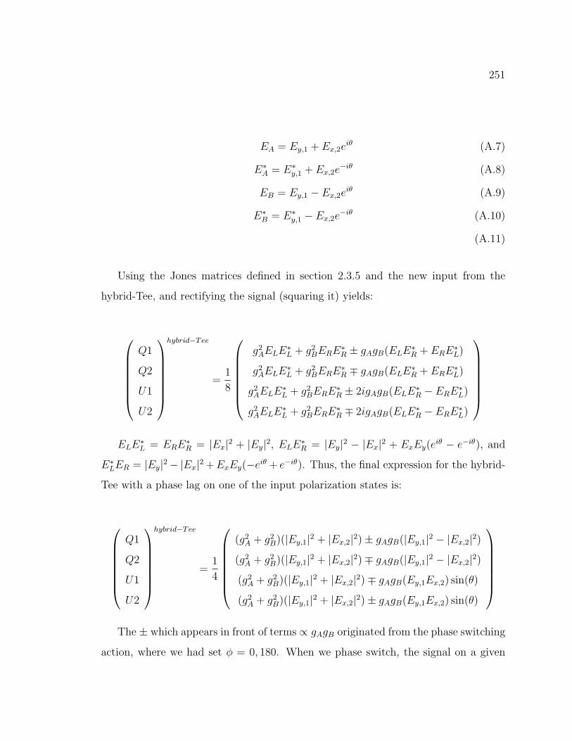
251
EA = Ey,1 + Ex,2eiθ (A.7)
E∗A = E
∗y,1 + Ex,2e
−iθ (A.8)
EB = Ey,1 − Ex,2eiθ (A.9)
E∗B = E
∗y,1 − Ex,2e
−iθ (A.10)
(A.11)
Using the Jones matrices defined in section 2.3.5 and the new input from the
hybrid-Tee, and rectifying the signal (squaring it) yields:
Q1
Q2
U1
U2
hybrid−Tee
=1
8
g2
AELE∗L + g
2
BERE∗R ± gAgB(ELE
∗R + ERE
∗L)
g2
AELE∗L + g
2
BERE∗R ∓ gAgB(ELE
∗R + ERE
∗L)
g2
AELE∗L + g
2
BERE∗R ± 2igAgB(ELE
∗R − ERE
∗L)
g2
AELE∗L + g
2
BERE∗R ∓ 2igAgB(ELE
∗R − ERE
∗L)
ELE∗L = ERE
∗R = |Ex|
2 + |Ey|2, ELE
∗R = |Ey|
2 − |Ex|2 + ExEy(eiθ − e
−iθ), and
E∗LER = |Ey|
2− |Ex|2 + ExEy(−e
iθ + e−iθ). Thus, the final expression for the hybrid-
Tee with a phase lag on one of the input polarization states is:
Q1
Q2
U1
U2
hybrid−Tee
=1
4
(g2
A + g2
B)(|Ey,1|2 + |Ex,2|
2) ± gAgB(|Ey,1|2 − |Ex,2|
2)
(g2
A + g2
B)(|Ey,1|2 + |Ex,2|
2)∓ gAgB(|Ey,1|2 − |Ex,2|
2)
(g2
A + g2
B)(|Ey,1|2 + |Ex,2|
2)∓ gAgB(Ey,1Ex,2) sin(θ)
(g2
A + g2
B)(|Ey,1|2 + |Ex,2|
2) ± gAgB(Ey,1Ex,2) sin(θ)
The ± which appears in front of terms ∝ gAgB originated from the phase switching
action, where we had set φ = 0, 180. When we phase switch, the signal on a given
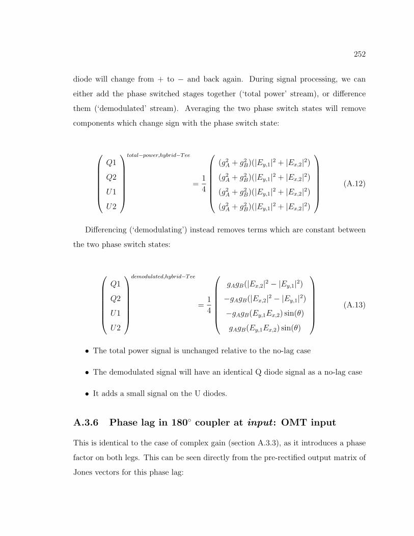
252
diode will change from + to − and back again. During signal processing, we can
either add the phase switched stages together (‘total power’ stream), or difference
them (‘demodulated’ stream). Averaging the two phase switch states will remove
components which change sign with the phase switch state:
Q1
Q2
U1
U2
total−power,hybrid−Tee
=1
4
(g2
A + g2
B)(|Ey,1|2 + |Ex,2|
2)
(g2
A + g2
B)(|Ey,1|2 + |Ex,2|
2)
(g2
A + g2
B)(|Ey,1|2 + |Ex,2|
2)
(g2
A + g2
B)(|Ey,1|2 + |Ex,2|
2)
(A.12)
Differencing (‘demodulating’) instead removes terms which are constant between
the two phase switch states:
Q1
Q2
U1
U2
demodulated,hybrid−Tee
=1
4
gAgB(|Ex,2|2 − |Ey,1|
2)
−gAgB(|Ex,2|2 − |Ey,1|
2)
−gAgB(Ey,1Ex,2) sin(θ)
gAgB(Ey,1Ex,2) sin(θ)
(A.13)
• The total power signal is unchanged relative to the no-lag case
• The demodulated signal will have an identical Q diode signal as a no-lag case
• It adds a small signal on the U diodes.
A.3.6 Phase lag in 180 coupler at input : OMT input
This is identical to the case of complex gain (section A.3.3), as it introduces a phase
factor on both legs. This can be seen directly from the pre-rectified output matrix of
Jones vectors for this phase lag:
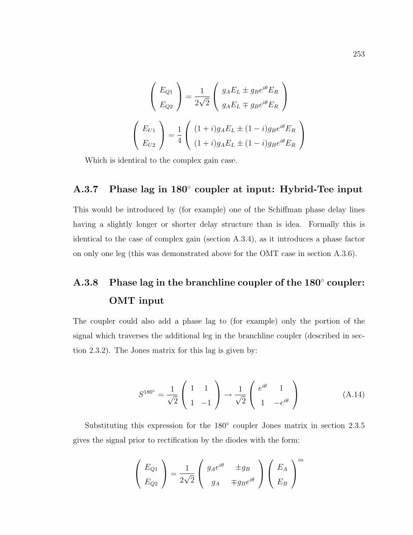
253
EQ1
EQ2
=1
2√
2
gAEL ± gBeiθER
gAEL ∓ gBeiθER
EU1
EU2
=1
4
(1 + i)gAEL ± (1− i)gBeiθER
(1 + i)gAEL ± (1− i)gBeiθER
Which is identical to the complex gain case.
A.3.7 Phase lag in 180 coupler at input: Hybrid-Tee input
This would be introduced by (for example) one of the Schiffman phase delay lines
having a slightly longer or shorter delay structure than is idea. Formally this is
identical to the case of complex gain (section A.3.4), as it introduces a phase factor
on only one leg (this was demonstrated above for the OMT case in section A.3.6).
A.3.8 Phase lag in the branchline coupler of the 180 coupler:
OMT input
The coupler could also add a phase lag to (for example) only the portion of the
signal which traverses the additional leg in the branchline coupler (described in sec-
tion 2.3.2). The Jones matrix for this lag is given by:
S180
=
1√
2
1 1
1 −1
→1√
2
eiθ 1
1 −eiθ
(A.14)
Substituting this expression for the 180 coupler Jones matrix in section 2.3.5
gives the signal prior to rectification by the diodes with the form:
EQ1
EQ2
=1
2√
2
gAeiθ ±gB
gA ∓gBeiθ
EA
EB
in
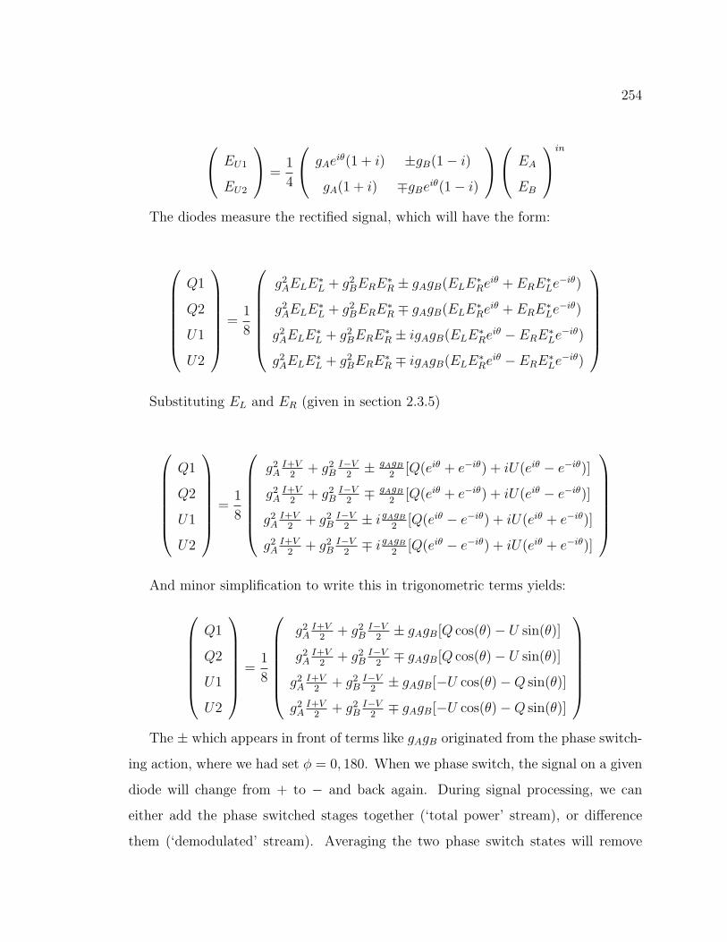
254
EU1
EU2
=1
4
gAeiθ(1 + i) ±gB(1− i)
gA(1 + i) ∓gBeiθ(1− i)
EA
EB
in
The diodes measure the rectified signal, which will have the form:
Q1
Q2
U1
U2
=
1
8
g2
AELE∗L + g
2
BERE∗R ± gAgB(ELE
∗Re
iθ + ERE∗Le
−iθ)
g2
AELE∗L + g
2
BERE∗R ∓ gAgB(ELE
∗Re
iθ + ERE∗Le
−iθ)
g2
AELE∗L + g
2
BERE∗R ± igAgB(ELE
∗Re
iθ − ERE∗Le
−iθ)
g2
AELE∗L + g
2
BERE∗R ∓ igAgB(ELE
∗Re
iθ − ERE∗Le
−iθ)
Substituting EL and ER (given in section 2.3.5)
Q1
Q2
U1
U2
=
1
8
g2
AI+V
2+ g
2
BI−V
2±
gAgB
2[Q(eiθ + e
−iθ) + iU(eiθ − e−iθ)]
g2
AI+V
2+ g
2
BI−V
2∓
gAgB
2[Q(eiθ + e
−iθ) + iU(eiθ − e−iθ)]
g2
AI+V
2+ g
2
BI−V
2± i
gAgB
2[Q(eiθ − e
−iθ) + iU(eiθ + e−iθ)]
g2
AI+V
2+ g
2
BI−V
2∓ i
gAgB
2[Q(eiθ − e
−iθ) + iU(eiθ + e−iθ)]
And minor simplification to write this in trigonometric terms yields:
Q1
Q2
U1
U2
=
1
8
g2
AI+V
2+ g
2
BI−V
2± gAgB[Q cos(θ)− U sin(θ)]
g2
AI+V
2+ g
2
BI−V
2∓ gAgB[Q cos(θ)− U sin(θ)]
g2
AI+V
2+ g
2
BI−V
2± gAgB[−U cos(θ)−Q sin(θ)]
g2
AI+V
2+ g
2
BI−V
2∓ gAgB[−U cos(θ)−Q sin(θ)]
The ± which appears in front of terms like gAgB originated from the phase switch-
ing action, where we had set φ = 0, 180. When we phase switch, the signal on a given
diode will change from + to − and back again. During signal processing, we can
either add the phase switched stages together (‘total power’ stream), or difference
them (‘demodulated’ stream). Averaging the two phase switch states will remove
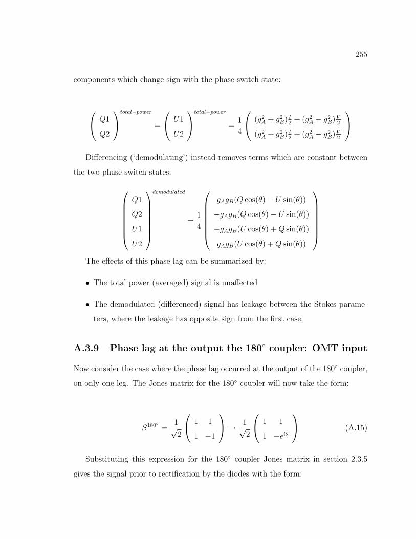
255
components which change sign with the phase switch state:
Q1
Q2
total−power
=
U1
U2
total−power
=1
4
(g2
A + g2
B) I2
+ (g2
A − g2
B)V2
(g2
A + g2
B) I2
+ (g2
A − g2
B)V2
Differencing (‘demodulating’) instead removes terms which are constant between
the two phase switch states:
Q1
Q2
U1
U2
demodulated
=1
4
gAgB(Q cos(θ)− U sin(θ))
−gAgB(Q cos(θ)− U sin(θ))
−gAgB(U cos(θ) + Q sin(θ))
gAgB(U cos(θ) + Q sin(θ))
The effects of this phase lag can be summarized by:
• The total power (averaged) signal is unaffected
• The demodulated (differenced) signal has leakage between the Stokes parame-
ters, where the leakage has opposite sign from the first case.
A.3.9 Phase lag at the output the 180 coupler: OMT input
Now consider the case where the phase lag occurred at the output of the 180 coupler,
on only one leg. The Jones matrix for the 180 coupler will now take the form:
S180
=
1√
2
1 1
1 −1
→1√
2
1 1
1 −eiθ
(A.15)
Substituting this expression for the 180 coupler Jones matrix in section 2.3.5
gives the signal prior to rectification by the diodes with the form:
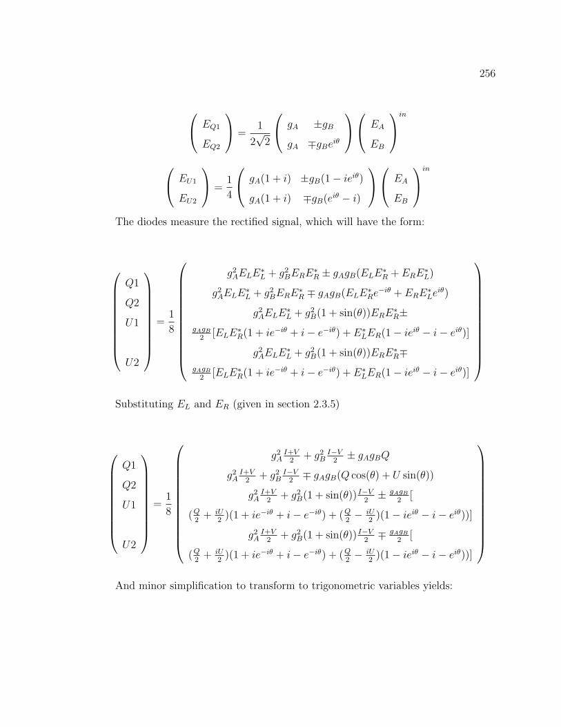
256
EQ1
EQ2
=1
2√
2
gA ±gB
gA ∓gBeiθ
EA
EB
in
EU1
EU2
=1
4
gA(1 + i) ±gB(1− ieiθ)
gA(1 + i) ∓gB(eiθ − i)
EA
EB
in
The diodes measure the rectified signal, which will have the form:
Q1
Q2
U1
U2
=1
8
g2
AELE∗L + g
2
BERE∗R ± gAgB(ELE
∗R + ERE
∗L)
g2
AELE∗L + g
2
BERE∗R ∓ gAgB(ELE
∗Re
−iθ + ERE∗Le
iθ)
g2
AELE∗L + g
2
B(1 + sin(θ))ERE∗R±
gAgB
2[ELE
∗R(1 + ie
−iθ + i− e−iθ) + E
∗LER(1− ie
iθ − i− eiθ)]
g2
AELE∗L + g
2
B(1 + sin(θ))ERE∗R∓
gAgB
2[ELE
∗R(1 + ie
−iθ + i− e−iθ) + E
∗LER(1− ie
iθ − i− eiθ)]
Substituting EL and ER (given in section 2.3.5)
Q1
Q2
U1
U2
=1
8
g2
AI+V
2+ g
2
BI−V
2± gAgBQ
g2
AI+V
2+ g
2
BI−V
2∓ gAgB(Q cos(θ) + U sin(θ))
g2
AI+V
2+ g
2
B(1 + sin(θ)) I−V2
±gAgB
2[
(Q2
+ iU2
)(1 + ie−iθ + i− e
−iθ) + (Q2−
iU2
)(1− ieiθ − i− e
iθ))]
g2
AI+V
2+ g
2
B(1 + sin(θ)) I−V2∓
gAgB
2[
(Q2
+ iU2
)(1 + ie−iθ + i− e
−iθ) + (Q2−
iU2
)(1− ieiθ − i− e
iθ))]
And minor simplification to transform to trigonometric variables yields:
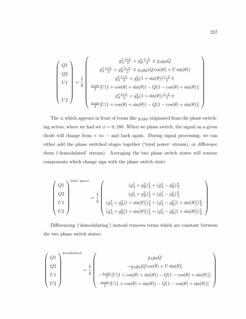
257
Q1
Q2
U1
U2
=1
8
g2
AI+V
2+ g
2
BI−V
2± gAgBQ
g2
AI+V
2+ g
2
BI−V
2∓ gAgB(Q cos(θ) + U sin(θ))
g2
AI+V
2+ g
2
B(1 + sin(θ)) I−V2∓
gAgB
2[U(1 + cos(θ) + sin(θ))−Q(1− cos(θ) + sin(θ))]
g2
AI+V
2+ g
2
B(1 + sin(θ)) I−V2±
gAgB
2[U(1 + cos(θ) + sin(θ))−Q(1− cos(θ) + sin(θ))]
The ± which appears in front of terms like gAgB originated from the phase switch-
ing action, where we had set φ = 0, 180. When we phase switch, the signal on a given
diode will change from + to − and back again. During signal processing, we can
either add the phase switched stages together (‘total power’ stream), or difference
them (‘demodulated’ stream). Averaging the two phase switch states will remove
components which change sign with the phase switch state:
Q1
Q2
U1
U2
total−power
=1
4
(g2
A + g2
B) I2
+ (g2
A − g2
B)V2
(g2
A + g2
B) I2
+ (g2
A − g2
B)V2
(g2
A + g2
B[1 + sin(θ)]) I2
+ (g2
A − g2
B[1 + sin(θ)])V2
(g2
A + g2
B[1 + sin(θ)]) I2
+ (g2
A − g2
B[1 + sin(θ)])V2
Differencing (‘demodulating’) instead removes terms which are constant between
the two phase switch states:
Q1
Q2
U1
U2
demodulated
=1
4
gAgBQ
−gAgB[Q cos(θ) + U sin(θ)]
−gAgB
2[U(1 + cos(θ) + sin(θ))−Q(1− cos(θ) + sin(θ))]
gAgB
2[U(1 + cos(θ) + sin(θ))−Q(1− cos(θ) + sin(θ))]
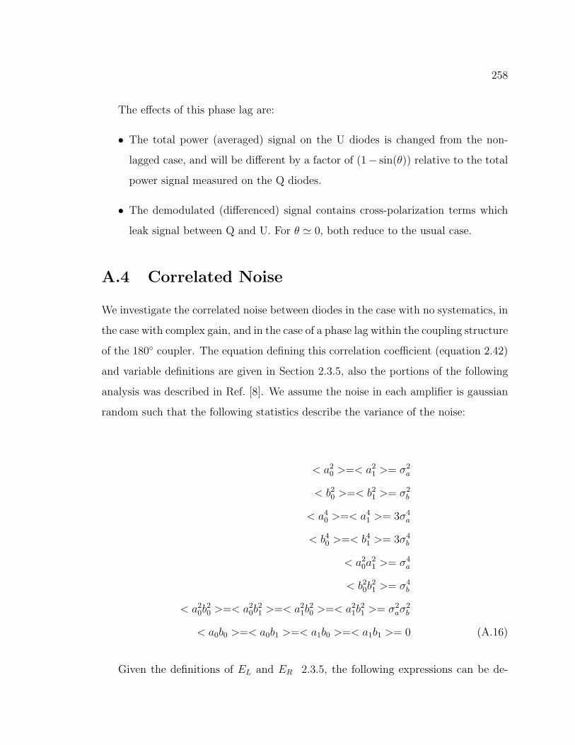
258
The effects of this phase lag are:
• The total power (averaged) signal on the U diodes is changed from the non-
lagged case, and will be different by a factor of (1− sin(θ)) relative to the total
power signal measured on the Q diodes.
• The demodulated (differenced) signal contains cross-polarization terms which
leak signal between Q and U. For θ 0, both reduce to the usual case.
A.4 Correlated Noise
We investigate the correlated noise between diodes in the case with no systematics, in
the case with complex gain, and in the case of a phase lag within the coupling structure
of the 180 coupler. The equation defining this correlation coefficient (equation 2.42)
and variable definitions are given in Section 2.3.5, also the portions of the following
analysis was described in Ref. [8]. We assume the noise in each amplifier is gaussian
random such that the following statistics describe the variance of the noise:
< a2
0>=< a
2
1>= σ
2
a
< b2
0>=< b
2
1>= σ
2
b
< a4
0>=< a
4
1>= 3σ4
a
< b4
0>=< b
4
1>= 3σ4
b
< a2
0a
2
1>= σ
4
a
< b2
0b2
1>= σ
4
b
< a2
0b2
0>=< a
2
0b2
1>=< a
2
1b2
0>=< a
2
1b2
1>= σ
2
aσ2
b
< a0b0 >=< a0b1 >=< a1b0 >=< a1b1 >= 0 (A.16)
Given the definitions of EL and ER 2.3.5, the following expressions can be de-
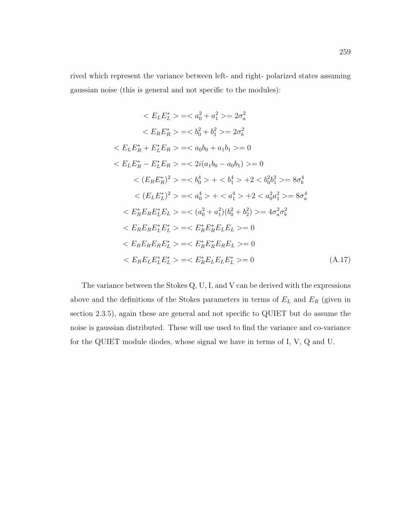
259
rived which represent the variance between left- and right- polarized states assuming
gaussian noise (this is general and not specific to the modules):
< ELE∗L > =< a
2
0+ a
2
1>= 2σ2
a
< ERE∗R > =< b
2
0+ b
2
1>= 2σ2
b
< ELE∗R + E
∗LER > =< a0b0 + a1b1 >= 0
< ELE∗R − E
∗LER > =< 2i(a1b0 − a0b1) >= 0
< (ERE∗R)2
> =< b4
0> + < b
4
1> +2 < b
2
0b2
1>= 8σ4
b
< (ELE∗L)2
> =< a4
0> + < a
4
1> +2 < a
2
0a
2
1>= 8σ4
a
< E∗RERE
∗LEL > =< (a2
0+ a
2
1)(b2
0+ b
2
2) >= 4σ2
aσ2
b
< ERERE∗LE
∗L > =< E
∗RE
∗RELEL >= 0
< ERERERE∗L > =< E
∗RE
∗REREL >= 0
< ERELE∗LE
∗L > =< E
∗RELELE
∗L >= 0 (A.17)
The variance between the Stokes Q, U, I, and V can be derived with the expressions
above and the definitions of the Stokes parameters in terms of EL and ER (given in
section 2.3.5), again these are general and not specific to QUIET but do assume the
noise is gaussian distributed. These will use used to find the variance and co-variance
for the QUIET module diodes, whose signal we have in terms of I, V, Q and U.
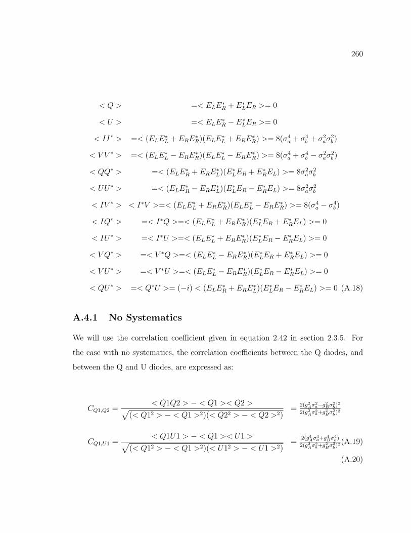
260
< Q > =< ELE∗R + E
∗LER >= 0
< U > =< ELE∗R − E
∗LER >= 0
< II∗
> =< (ELE∗L + ERE
∗R)(ELE
∗L + ERE
∗R) >= 8(σ4
a + σ4
b + σ2
aσ2
b )
< V V∗
> =< (ELE∗L − ERE
∗R)(ELE
∗L − ERE
∗R) >= 8(σ4
a + σ4
b − σ2
aσ2
b )
< QQ∗
> =< (ELE∗R + ERE
∗L)(E∗
LER + E∗REL) >= 8σ2
aσ2
b
< UU∗
> =< (ELE∗R − ERE
∗L)(E∗
LER − E∗REL) >= 8σ2
aσ2
b
< IV∗
> < I∗V >=< (ELE
∗L + ERE
∗R)(ELE
∗L − ERE
∗R) >= 8(σ4
a − σ4
b )
< IQ∗
> =< I∗Q >=< (ELE
∗L + ERE
∗R)(E∗
LER + E∗REL) >= 0
< IU∗
> =< I∗U >=< (ELE
∗L + ERE
∗R)(E∗
LER − E∗REL) >= 0
< V Q∗
> =< V∗Q >=< (ELE
∗L − ERE
∗R)(E∗
LER + E∗REL) >= 0
< V U∗
> =< V∗U >=< (ELE
∗L − ERE
∗R)(E∗
LER − E∗REL) >= 0
< QU∗
> =< Q∗U >= (−i) < (ELE
∗R + ERE
∗L)(E∗
LER − E∗REL) >= 0 (A.18)
A.4.1 No Systematics
We will use the correlation coefficient given in equation 2.42 in section 2.3.5. For
the case with no systematics, the correlation coefficients between the Q diodes, and
between the Q and U diodes, are expressed as:
CQ1,Q2 =< Q1Q2 > − < Q1 >< Q2 >
(< Q12 > − < Q1 >2)(< Q22 > − < Q2 >2)=
2(g2Aσ2
a−g2Bσ2
b )2
2(g2Aσ2
a+g2Bσ2
b )2
CQ1,U1 =< Q1U1 > − < Q1 >< U1 >
(< Q12 > − < Q1 >2)(< U12 > − < U1 >2)=
2(g4Aσ4
a+g4Bσ4
b )
2(g2Aσ2
a+g2Bσ2
b )2(A.19)
(A.20)
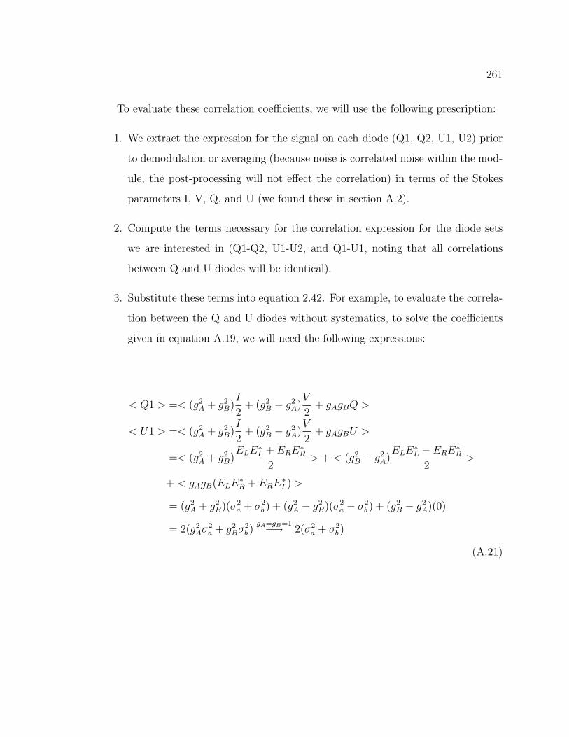
261
To evaluate these correlation coefficients, we will use the following prescription:
1. We extract the expression for the signal on each diode (Q1, Q2, U1, U2) prior
to demodulation or averaging (because noise is correlated noise within the mod-
ule, the post-processing will not effect the correlation) in terms of the Stokes
parameters I, V, Q, and U (we found these in section A.2).
2. Compute the terms necessary for the correlation expression for the diode sets
we are interested in (Q1-Q2, U1-U2, and Q1-U1, noting that all correlations
between Q and U diodes will be identical).
3. Substitute these terms into equation 2.42. For example, to evaluate the correla-
tion between the Q and U diodes without systematics, to solve the coefficients
given in equation A.19, we will need the following expressions:
< Q1 > =< (g2
A + g2
B)I
2+ (g2
B − g2
A)V
2+ gAgBQ >
< U1 > =< (g2
A + g2
B)I
2+ (g2
B − g2
A)V
2+ gAgBU >
=< (g2
A + g2
B)ELE
∗L + ERE
∗R
2> + < (g2
B − g2
A)ELE
∗L − ERE
∗R
2>
+ < gAgB(ELE∗R + ERE
∗L) >
= (g2
A + g2
B)(σ2
a + σ2
b ) + (g2
A − g2
B)(σ2
a − σ2
b ) + (g2
B − g2
A)(0)
= 2(g2
Aσ2
a + g2
Bσ2
b )gA=gB=1
−→ 2(σ2
a + σ2
b )
(A.21)
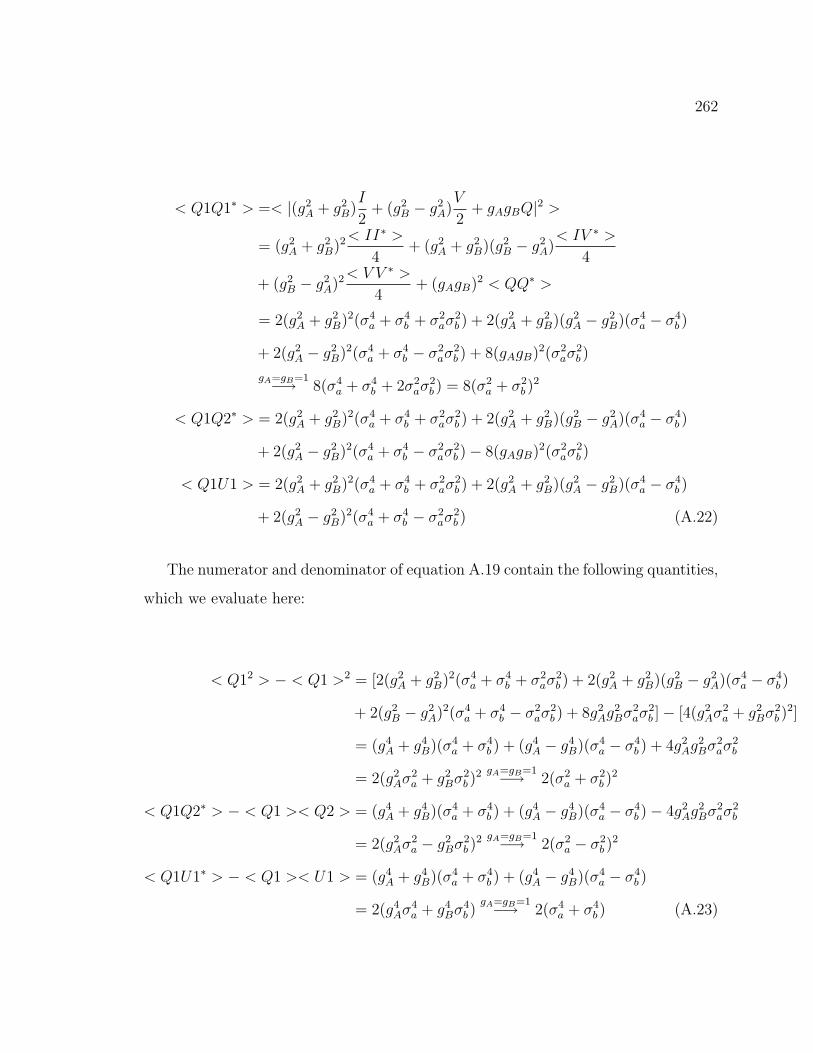
262
< Q1Q1∗ > =< |(g2
A + g2
B)I
2+ (g2
B − g2
A)V
2+ gAgBQ|
2>
= (g2
A + g2
B)2< II
∗>
4+ (g2
A + g2
B)(g2
B − g2
A)< IV
∗>
4
+ (g2
B − g2
A)2< V V
∗>
4+ (gAgB)2
< QQ∗
>
= 2(g2
A + g2
B)2(σ4
a + σ4
b + σ2
aσ2
b ) + 2(g2
A + g2
B)(g2
A − g2
B)(σ4
a − σ4
b )
+ 2(g2
A − g2
B)2(σ4
a + σ4
b − σ2
aσ2
b ) + 8(gAgB)2(σ2
aσ2
b )
gA=gB=1
−→ 8(σ4
a + σ4
b + 2σ2
aσ2
b ) = 8(σ2
a + σ2
b )2
< Q1Q2∗ > = 2(g2
A + g2
B)2(σ4
a + σ4
b + σ2
aσ2
b ) + 2(g2
A + g2
B)(g2
B − g2
A)(σ4
a − σ4
b )
+ 2(g2
A − g2
B)2(σ4
a + σ4
b − σ2
aσ2
b )− 8(gAgB)2(σ2
aσ2
b )
< Q1U1 > = 2(g2
A + g2
B)2(σ4
a + σ4
b + σ2
aσ2
b ) + 2(g2
A + g2
B)(g2
A − g2
B)(σ4
a − σ4
b )
+ 2(g2
A − g2
B)2(σ4
a + σ4
b − σ2
aσ2
b ) (A.22)
The numerator and denominator of equation A.19 contain the following quantities,
which we evaluate here:
< Q12> − < Q1 >
2 = [2(g2
A + g2
B)2(σ4
a + σ4
b + σ2
aσ2
b ) + 2(g2
A + g2
B)(g2
B − g2
A)(σ4
a − σ4
b )
+ 2(g2
B − g2
A)2(σ4
a + σ4
b − σ2
aσ2
b ) + 8g2
Ag2
Bσ2
aσ2
b ]− [4(g2
Aσ2
a + g2
Bσ2
b )2]
= (g4
A + g4
B)(σ4
a + σ4
b ) + (g4
A − g4
B)(σ4
a − σ4
b ) + 4g2
Ag2
Bσ2
aσ2
b
= 2(g2
Aσ2
a + g2
Bσ2
b )2 gA=gB=1
−→ 2(σ2
a + σ2
b )2
< Q1Q2∗ > − < Q1 >< Q2 > = (g4
A + g4
B)(σ4
a + σ4
b ) + (g4
A − g4
B)(σ4
a − σ4
b )− 4g2
Ag2
Bσ2
aσ2
b
= 2(g2
Aσ2
a − g2
Bσ2
b )2 gA=gB=1
−→ 2(σ2
a − σ2
b )2
< Q1U1∗ > − < Q1 >< U1 > = (g4
A + g4
B)(σ4
a + σ4
b ) + (g4
A − g4
B)(σ4
a − σ4
b )
= 2(g4
Aσ4
a + g4
Bσ4
b )gA=gB=1
−→ 2(σ4
a + σ4
b ) (A.23)
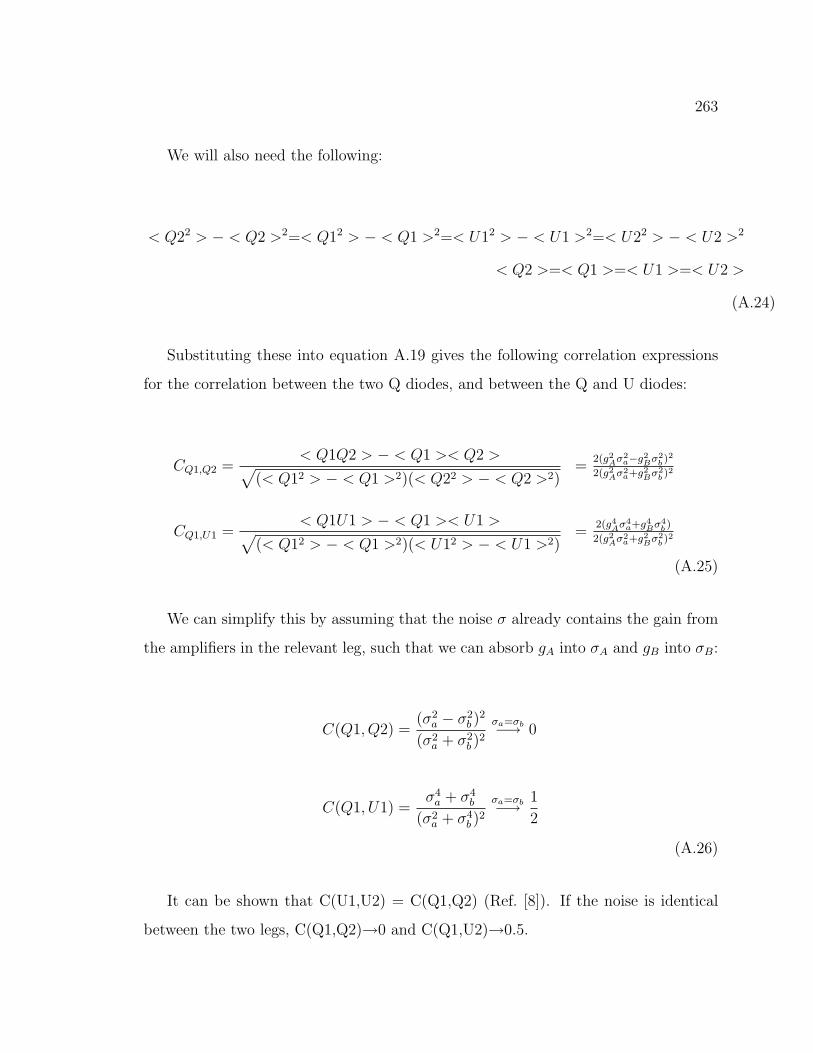
263
We will also need the following:
< Q22> − < Q2 >
2=< Q12> − < Q1 >
2=< U12> − < U1 >
2=< U22> − < U2 >
2
< Q2 >=< Q1 >=< U1 >=< U2 >
(A.24)
Substituting these into equation A.19 gives the following correlation expressions
for the correlation between the two Q diodes, and between the Q and U diodes:
CQ1,Q2 =< Q1Q2 > − < Q1 >< Q2 >
(< Q12 > − < Q1 >2)(< Q22 > − < Q2 >2)=
2(g2Aσ2
a−g2Bσ2
b )2
2(g2Aσ2
a+g2Bσ2
b )2
CQ1,U1 =< Q1U1 > − < Q1 >< U1 >
(< Q12 > − < Q1 >2)(< U12 > − < U1 >2)=
2(g4Aσ4
a+g4Bσ4
b )
2(g2Aσ2
a+g2Bσ2
b )2
(A.25)
We can simplify this by assuming that the noise σ already contains the gain from
the amplifiers in the relevant leg, such that we can absorb gA into σA and gB into σB:
C(Q1, Q2) =(σ2
a − σ2
b )2
(σ2a + σ
2
b )2
σa=σb−→ 0
C(Q1, U1) =σ
4
a + σ4
b
(σ2a + σ
4
b )2
σa=σb−→
1
2
(A.26)
It can be shown that C(U1,U2) = C(Q1,Q2) (Ref. [8]). If the noise is identical
between the two legs, C(Q1,Q2)→0 and C(Q1,U2)→0.5.
264
A.4.2 Complex Gain
We repeat the prescription outlined above in section A.4.1, however this time instead
of using the expressions for the diode measurement from a no-systematics case, we
will use the expression for the diode measurement derived assuming complex gain
(section A.3.3). In this case, the inputs to the correlation expression given by equa-
tion 2.42.
< Q1 >imperf =< (g2
A + g2
B)I
2+ (g2
A − g2
B)V
2+ gAgB(Q cos(θ) + U sin(θ) >=< Q1 >
< Q1Q2∗ >imperf =< [(g2
A + g2
B)I
2+ (g2
A − g2
B)V
2+ gAgB(Q cos(θ) + U sin(θ))]×
[(g2
A + g2
B)I
2+ (g2
A − g2
B)V
2− gAgB(Q cos(θ) + U sin(θ))]∗ >
= 2(g2
A + g2
B)2(σ4
a + σ4
b + σ2
aσ2
b ) + 2(g2
A + g2
B)(g2
A − g2
B)(σ4
a − σ4
b )
+ 2(g2
A − g2
B)2(σ4
a + σ4
b − σ2
aσ2
b )− 8(gAgB)2(σ2
aσ2
b )
< Q1U1∗ >imperf =< [(g2
A + g2
B)I
2+ (g2
A − g2
B)V
2+ gAgB(Q cos(θ) + U sin(θ))]×
[(g2
A + g2
B)I
2+ (g2
A − g2
B)V
2+ gAgB(U cos(θ)−Q sin(θ))]× >
= 2(g2
A + g2
B)2(σ4
a + σ4
b + σ2
aσ2
b ) + 2(g2
A + g2
B)(g2
A − g2
B)(σ4
a − σ4
b )
+ 2(g2
A − g2
B)2(σ4
a + σ4
b − σ2
aσ2
b ) (A.27)
These expressions are identical to the non-phase lagged version, hence complex
gain does not affect correlated noise.
A.4.3 Phase Lag at the Input to the 180 Coupler
As we noted in section A.3.6, the expression for the diode signal for this case is
identical to the complex gain diode signal, hence the correlation coefficient will also
be the same. Hence, this systematic also has no effect on correlated noise.
265
A.4.4 Phase Lag in the Branchline Coupler
We repeat the prescription outlined above in section A.4.1, however this time instead
of using the expressions for the diode measurement from a no-systematics case, we
will use the expression for the diode measurement derived assuming that the 180
coupler added a phase lag to the portion of the signal which was delayed by the extra
λ/4 section of the branchline coupler (section A.3.9). We find the expressions for
Q1, Q2, U1, and U2 in terms of Stokes Q, U, I, and V parameters from equations
presented in section A.3.8. We will use these to derive an expression for the terms
for equation 2.42 with the diode signal:
< Q1Q2∗ >imperf =< [(g2
A + g2
B)I
2+ (g2
A − g2
B)V
2+ gAgB(Q cos(θ)− U sin(θ))]×
[(g2
A + g2
B)I
2+ (g2
A − g2
B)V
2− gAgB(Q cos(θ)− U sin(θ))]∗ >
= 2(g2
A + g2
B)2(σ4
a + σ4
b + σ2
aσ2
b ) + 2(g2
A + g2
B)(g2
A − g2
B)(σ4
a − σ4
b )
+ 2(g2
A − g2
B)2(σ4
a + σ4
b − σ2
aσ2
b )− 8(gAgB)2(σ2
aσ2
b )
< Q1U1∗ >imperf =< [(g2
A + g2
B)I
2+ (g2
A − g2
B)V
2+ gAgB(Q cos(θ)− U sin(θ))]×
[(g2
A + g2
B)I
2+ (g2
A − g2
B)V
2+ gAgB(U cos(θ) + Q sin(θ))]× >
= 2(g2
A + g2
B)2(σ4
a + σ4
b + σ2
aσ2
b ) + 2(g2
A + g2
B)(g2
A − g2
B)(σ4
a − σ4
b )
+ 2(g2
A − g2
B)2(σ4
a + σ4
b − σ2
aσ2
b ) (A.28)
These terms are identical to those derived for no systematics (section A.4.1), so
although the diode signal has a slightly different expression from the cases considered
above, this case also does not change the correlated noise in the module.
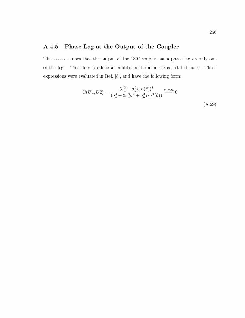
266
A.4.5 Phase Lag at the Output of the Coupler
This case assumes that the output of the 180 coupler has a phase lag on only one
of the legs. This does produce an additional term in the correlated noise. These
expressions were evaluated in Ref. [8], and have the following form:
C(U1, U2) =(σ2
a − σ2
b cos(θ))2
(σ4a + 2σ2
aσ2
b + σ4
b cos2(θ))σa=σb−→ 0
(A.29)

Appendix B
Bandpasses: Site measurements
B.1 Bandpasses from Site Measurements
During the course of bandpass measurements at the site, we took 35 separate bandsweeps
over two days. As mentioned in section 3.2.2, the U diodes were not well measured
by site data, so I present only data from the Q-diodes. Figures B-1- B-2 show the Q1
and Q2 diode bandpasses for all modules, where each bandpass has been normalized
by the area under the bandpass to bring them to a common scale. A bandsweep is
only included if the computed bandwidth is between 6-9 GHz and if there were no
drop-outs (portions where the signal drops dramatically due to interference between
metal components in the testing setup).
Figures B-3- B-4 show the averaged bandpasses for the Q1 and Q2 diodes for
all modules from the normalized bandpasses which passed the criteria given above.
The average is computed frequency point by frequency point, and the errors are
computed from the standard deviation, also per frequency point. The given error
bars are treated as statistical, although they contain the systematic error from the
differences between the two days. If a module had only one day of data which passed
the criteria, the errors quoted are 4×10⁻⁴, which is the mean of the error values for
modules which had valid sweeps taken on both days.
267
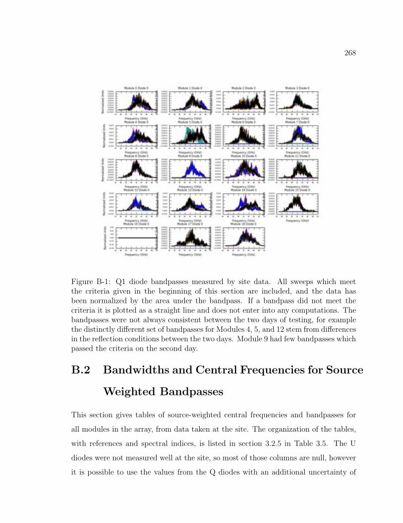
268
Figure B-1: Q1 diode bandpasses measured by site data. All sweeps which meetthe criteria given in the beginning of this section are included, and the data hasbeen normalized by the area under the bandpass. If a bandpass did not meet thecriteria it is plotted as a straight line and does not enter into any computations. Thebandpasses were not always consistent between the two days of testing, for examplethe distinctly different set of bandpasses for Modules 4, 5, and 12 stem from differencesin the reflection conditions between the two days. Module 9 had few bandpasses whichpassed the criteria on the second day.
B.2 Bandwidths and Central Frequencies for Source
Weighted Bandpasses
This section gives tables of source-weighted central frequencies and bandpasses for
all modules in the array, from data taken at the site. The organization of the tables,
with references and spectral indices, is listed in section 3.2.5 in Table 3.5. The U
diodes were not measured well at the site, so most of those columns are null, however
it is possible to use the values from the Q diodes with an additional uncertainty of
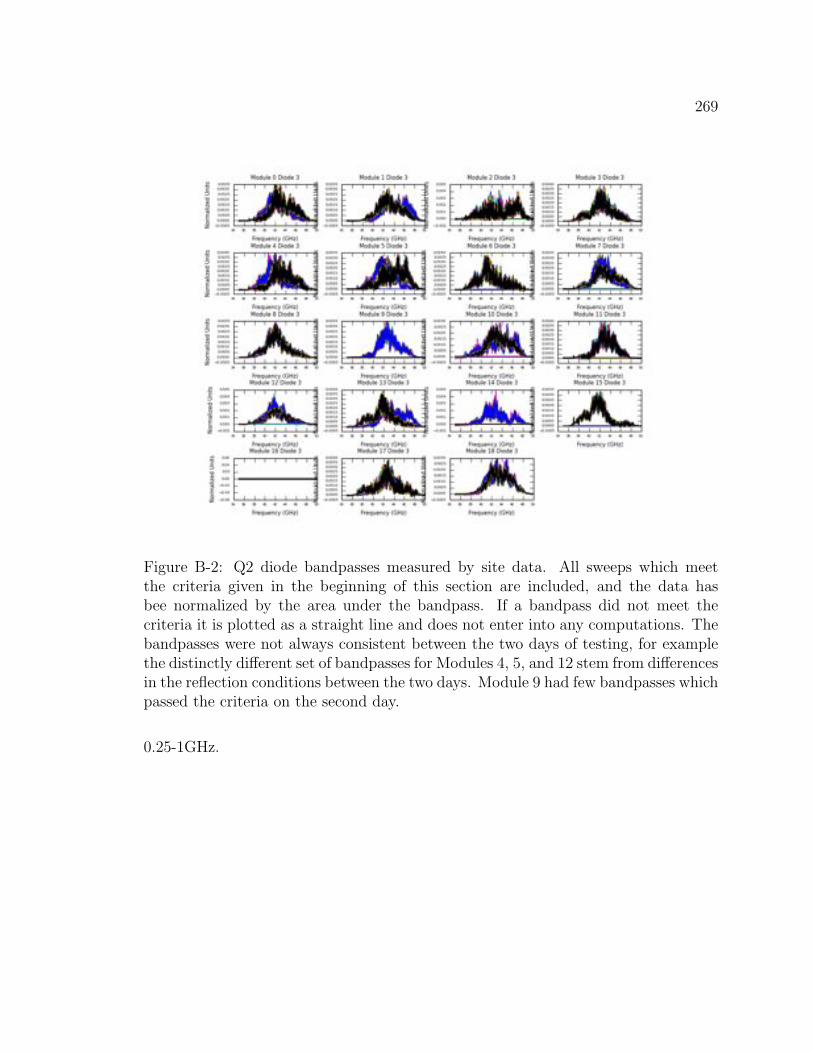
269
Figure B-2: Q2 diode bandpasses measured by site data. All sweeps which meetthe criteria given in the beginning of this section are included, and the data hasbee normalized by the area under the bandpass. If a bandpass did not meet thecriteria it is plotted as a straight line and does not enter into any computations. Thebandpasses were not always consistent between the two days of testing, for examplethe distinctly different set of bandpasses for Modules 4, 5, and 12 stem from differencesin the reflection conditions between the two days. Module 9 had few bandpasses whichpassed the criteria on the second day.
0.25-1GHz.
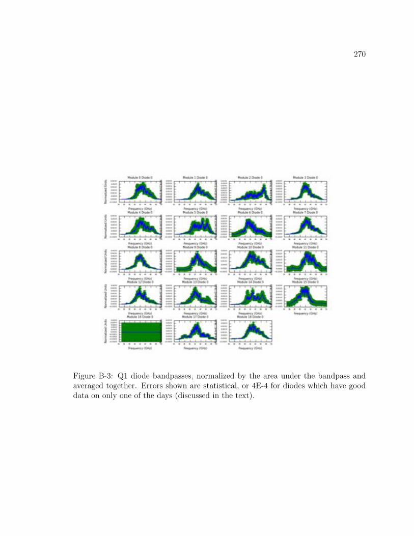
270
Figure B-3: Q1 diode bandpasses, normalized by the area under the bandpass andaveraged together. Errors shown are statistical, or 4E-4 for diodes which have gooddata on only one of the days (discussed in the text).
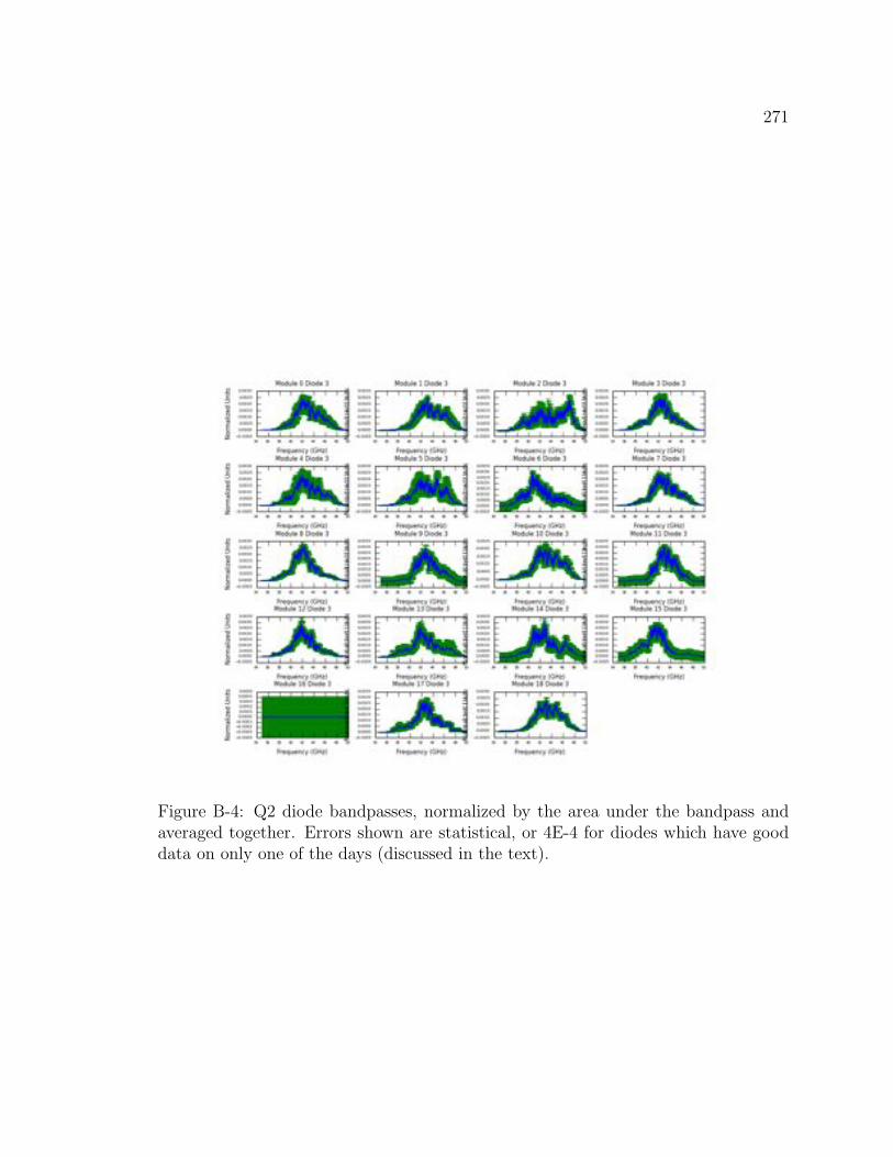
271
Figure B-4: Q2 diode bandpasses, normalized by the area under the bandpass andaveraged together. Errors shown are statistical, or 4E-4 for diodes which have gooddata on only one of the days (discussed in the text).
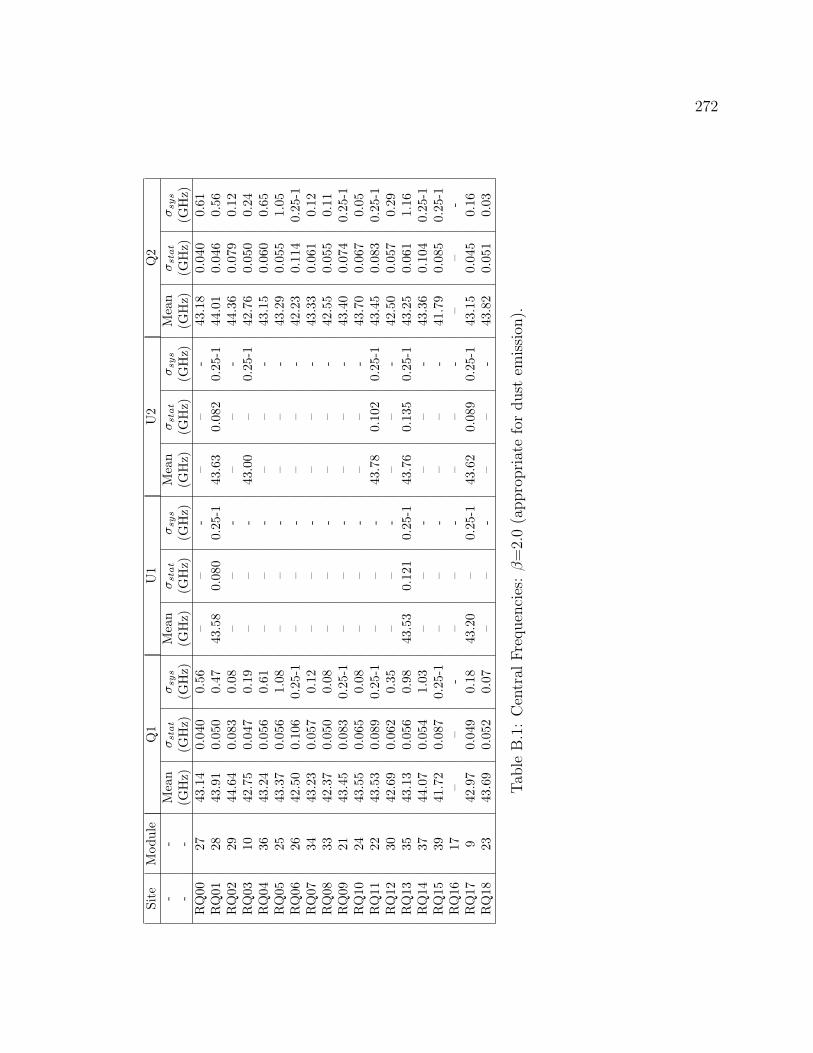
272
Site
Mod
ule
Q1
U1
U2
Q2
--
Mea
nσ
sta
tσ
sys
Mea
nσ
sta
tσ
sys
Mea
nσ
sta
tσ
sys
Mea
nσ
sta
tσ
sys
--
(GH
z)(G
Hz)
(GH
z)(G
Hz)
(GH
z)(G
Hz)
(GH
z)(G
Hz)
(GH
z)(G
Hz)
(GH
z)(G
Hz)
RQ
0027
43.1
40.
040
0.56
––
-–
–-
43.1
80.
040
0.61
RQ
0128
43.9
10.
050
0.47
43.5
80.
080
0.25
-143
.63
0.08
20.
25-1
44.0
10.
046
0.56
RQ
0229
44.6
40.
083
0.08
––
-–
–-
44.3
60.
079
0.12
RQ
0310
42.7
50.
047
0.19
––
-43
.00
–0.
25-1
42.7
60.
050
0.24
RQ
0436
43.2
40.
056
0.61
––
-–
–-
43.1
50.
060
0.65
RQ
0525
43.3
70.
056
1.08
––
-–
–-
43.2
90.
055
1.05
RQ
0626
42.5
00.
106
0.25
-1–
–-
––
-42
.23
0.11
40.
25-1
RQ
0734
43.2
30.
057
0.12
––
-–
–-
43.3
30.
061
0.12
RQ
0833
42.3
70.
050
0.08
––
-–
–-
42.5
50.
055
0.11
RQ
0921
43.4
50.
083
0.25
-1–
–-
––
-43
.40
0.07
40.
25-1
RQ
1024
43.5
50.
065
0.08
––
-–
–-
43.7
00.
067
0.05
RQ
1122
43.5
30.
089
0.25
-1–
–-
43.7
80.
102
0.25
-143
.45
0.08
30.
25-1
RQ
1230
42.6
90.
062
0.35
––
-–
–-
42.5
00.
057
0.29
RQ
1335
43.1
30.
056
0.98
43.5
30.
121
0.25
-143
.76
0.13
50.
25-1
43.2
50.
061
1.16
RQ
1437
44.0
70.
054
1.03
––
-–
–-
43.3
60.
104
0.25
-1R
Q15
3941
.72
0.08
70.
25-1
––
-–
–-
41.7
90.
085
0.25
-1R
Q16
17–
–-
––
-–
–-
––
-R
Q17
942
.97
0.04
90.
1843
.20
–0.
25-1
43.6
20.
089
0.25
-143
.15
0.04
50.
16R
Q18
2343
.69
0.05
20.
07–
–-
––
-43
.82
0.05
10.
03
Tab
leB
.1:
Cen
tral
Fre
quen
cies
:β=
2.0
(appro
pri
ate
for
dust
emis
sion
).
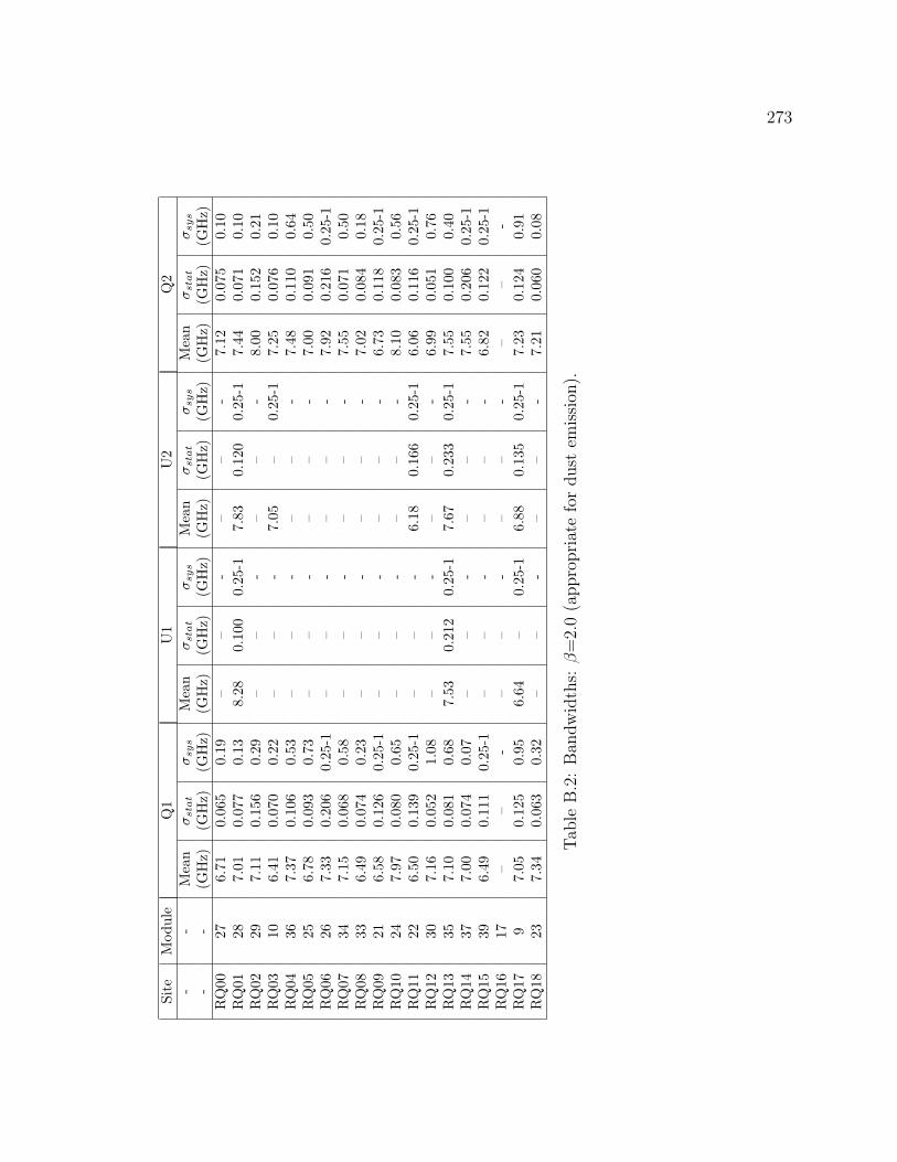
273
Site
Mod
ule
Q1
U1
U2
Q2
--
Mea
nσ
sta
tσ
sys
Mea
nσ
sta
tσ
sys
Mea
nσ
sta
tσ
sys
Mea
nσ
sta
tσ
sys
--
(GH
z)(G
Hz)
(GH
z)(G
Hz)
(GH
z)(G
Hz)
(GH
z)(G
Hz)
(GH
z)(G
Hz)
(GH
z)(G
Hz)
RQ
0027
6.71
0.06
50.
19–
–-
––
-7.
120.
075
0.10
RQ
0128
7.01
0.07
70.
138.
280.
100
0.25
-17.
830.
120
0.25
-17.
440.
071
0.10
RQ
0229
7.11
0.15
60.
29–
–-
––
-8.
000.
152
0.21
RQ
0310
6.41
0.07
00.
22–
–-
7.05
–0.
25-1
7.25
0.07
60.
10R
Q04
367.
370.
106
0.53
––
-–
–-
7.48
0.11
00.
64R
Q05
256.
780.
093
0.73
––
-–
–-
7.00
0.09
10.
50R
Q06
267.
330.
206
0.25
-1–
–-
––
-7.
920.
216
0.25
-1R
Q07
347.
150.
068
0.58
––
-–
–-
7.55
0.07
10.
50R
Q08
336.
490.
074
0.23
––
-–
–-
7.02
0.08
40.
18R
Q09
216.
580.
126
0.25
-1–
–-
––
-6.
730.
118
0.25
-1R
Q10
247.
970.
080
0.65
––
-–
–-
8.10
0.08
30.
56R
Q11
226.
500.
139
0.25
-1–
–-
6.18
0.16
60.
25-1
6.06
0.11
60.
25-1
RQ
1230
7.16
0.05
21.
08–
–-
––
-6.
990.
051
0.76
RQ
1335
7.10
0.08
10.
687.
530.
212
0.25
-17.
670.
233
0.25
-17.
550.
100
0.40
RQ
1437
7.00
0.07
40.
07–
–-
––
-7.
550.
206
0.25
-1R
Q15
396.
490.
111
0.25
-1–
–-
––
-6.
820.
122
0.25
-1R
Q16
17–
–-
––
-–
–-
––
-R
Q17
97.
050.
125
0.95
6.64
–0.
25-1
6.88
0.13
50.
25-1
7.23
0.12
40.
91R
Q18
237.
340.
063
0.32
––
-–
–-
7.21
0.06
00.
08
Tab
leB
.2:
Ban
dw
idth
s:β=
2.0
(appro
pri
ate
for
dust
emis
sion
).
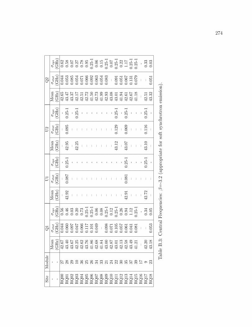
274
Site
Mod
ule
Q1
U1
U2
Q2
--
Mea
nσ
sta
tσ
sys
Mea
nσ
sta
tσ
sys
Mea
nσ
sta
tσ
sys
Mea
nσ
sta
tσ
sys
--
(GH
z)(G
Hz)
(GH
z)(G
Hz)
(GH
z)(G
Hz)
(GH
z)(G
Hz)
(GH
z)(G
Hz)
(GH
z)(G
Hz)
RQ
0027
42.6
70.
044
0.56
––
-–
–-
42.6
50.
044
0.62
RQ
0128
43.4
00.
060
0.46
42.9
20.
087
0.25
-142
.95
0.09
50.
25-1
43.4
70.
053
0.58
RQ
0229
43.6
70.
097
0.03
––
-–
–-
43.3
70.
085
0.07
RQ
0310
42.2
50.
047
0.20
––
-42
.25
–0.
25-1
42.1
70.
054
0.27
RQ
0436
42.6
20.
066
0.73
––
-–
–-
42.5
10.
071
0.78
RQ
0525
43.7
60.
117
0.25
-1–
–-
––
-42
.72
0.06
60.
95R
Q06
2641
.86
0.10
10.
25-1
––
-–
–-
41.5
00.
092
0.25
-1R
Q07
3442
.68
0.04
90.
06–
–-
––
-42
.73
0.06
30.
06R
Q08
3341
.84
–0.
08–
–-
––
-41
.99
0.05
40.
15R
Q09
2143
.00
0.09
80.
25-1
––
-–
–-
42.9
30.
083
0.25
-1R
Q10
2442
.87
0.07
10.
12–
–-
––
-43
.08
–0.
07R
Q11
2243
.01
0.10
50.
25-1
––
-43
.12
0.12
90.
25-1
43.0
10.
091
0.25
-1R
Q12
3042
.13
0.05
70.
26–
–-
––
-41
.94
0.05
10.
22R
Q13
3542
.58
0.06
10.
9442
.91
0.08
10.
25-1
43.0
70.
069
0.25
-142
.61
0.06
71.
17R
Q14
3743
.49
0.04
11.
12–
–-
––
-42
.67
0.13
10.
25-1
RQ
1539
41.2
10.
081
0.25
-1–
–-
––
-41
.18
0.07
90.
25-1
RQ
1617
––
-–
–-
––
-–
–-
RQ
179
42.2
0–
0.34
42.7
2–
0.25
-143
.10
0.11
60.
25-1
42.5
1–
0.33
RQ
1823
43.1
80.
053
0.05
––
-–
–-
43.3
20.
051
0.03
Tab
leB
.3:
Cen
tral
Fre
quen
cies
:β=
-3.2
(appro
pri
ate
for
soft
synch
rotr
onem
issi
on).
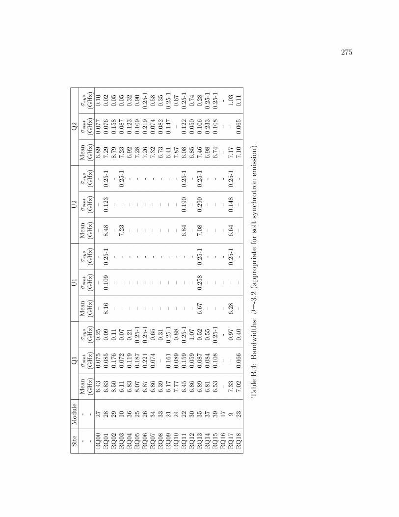
275
Site
Mod
ule
Q1
U1
U2
Q2
--
Mea
nσ
sta
tσ
sys
Mea
nσ
sta
tσ
sys
Mea
nσ
sta
tσ
sys
Mea
nσ
sta
tσ
sys
--
(GH
z)(G
Hz)
(GH
z)(G
Hz)
(GH
z)(G
Hz)
(GH
z)(G
Hz)
(GH
z)(G
Hz)
(GH
z)(G
Hz)
RQ
0027
6.43
0.07
50.
25–
–-
––
-6.
890.
077
0.10
RQ
0128
6.83
0.08
50.
098.
160.
109
0.25
-18.
480.
123
0.25
-17.
290.
076
0.02
RQ
0229
8.50
0.17
60.
11–
–-
––
-8.
790.
158
0.05
RQ
0310
6.11
0.07
20.
07–
–-
7.23
–0.
25-1
7.23
0.08
70.
05R
Q04
366.
830.
119
0.21
––
-–
–-
6.92
0.12
30.
32R
Q05
258.
070.
187
0.25
-1–
–-
––
-7.
280.
109
0.90
RQ
0626
6.87
0.22
10.
25-1
––
-–
–-
7.26
0.21
90.
25-1
RQ
0734
6.86
0.07
40.
65–
–-
––
-7.
320.
074
0.58
RQ
0833
6.39
–0.
31–
–-
––
-6.
730.
082
0.35
RQ
0921
6.17
0.16
10.
25-1
––
-–
–-
6.41
0.14
70.
25-1
RQ
1024
7.77
0.08
90.
88–
–-
––
-7.
87–
0.67
RQ
1122
6.45
0.15
90.
25-1
––
-6.
840.
190
0.25
-16.
080.
122
0.25
-1R
Q12
306.
860.
059
1.07
––
-–
–-
6.85
0.05
00.
74R
Q13
356.
890.
087
0.52
6.67
0.25
80.
25-1
7.08
0.29
00.
25-1
7.46
0.10
60.
28R
Q14
376.
810.
084
0.55
––
-–
–-
6.98
0.23
30.
25-1
RQ
1539
6.53
0.10
80.
25-1
––
-–
–-
6.74
0.10
80.
25-1
RQ
1617
––
-–
–-
––
-–
–-
RQ
179
7.33
–0.
976.
28–
0.25
-16.
640.
148
0.25
-17.
17–
1.03
RQ
1823
7.02
0.06
60.
40–
–-
––
-7.
100.
065
0.11
Tab
leB
.4:
Ban
dw
idth
s:β=
-3.2
(appro
pri
ate
for
soft
synch
rotr
onem
issi
on).
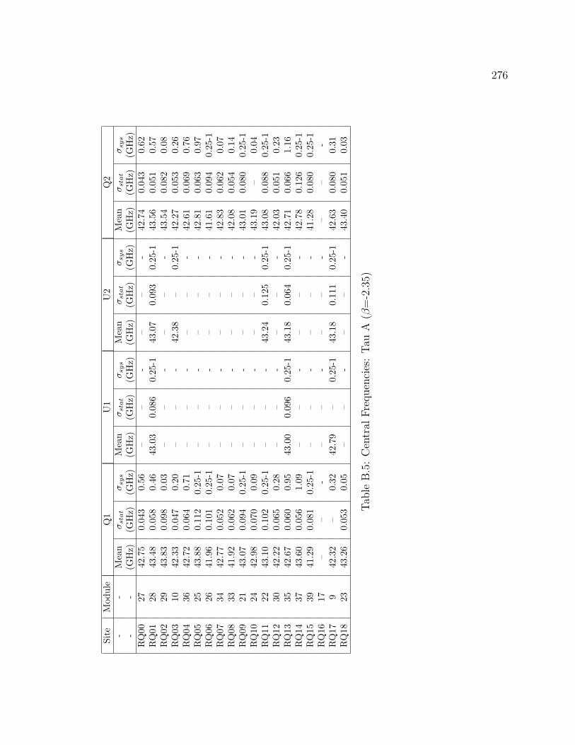
276
Site
Mod
ule
Q1
U1
U2
Q2
--
Mea
nσ
sta
tσ
sys
Mea
nσ
sta
tσ
sys
Mea
nσ
sta
tσ
sys
Mea
nσ
sta
tσ
sys
--
(GH
z)(G
Hz)
(GH
z)(G
Hz)
(GH
z)(G
Hz)
(GH
z)(G
Hz)
(GH
z)(G
Hz)
(GH
z)(G
Hz)
RQ
0027
42.7
50.
043
0.56
––
-–
–-
42.7
40.
043
0.62
RQ
0128
43.4
80.
058
0.46
43.0
30.
086
0.25
-143
.07
0.09
30.
25-1
43.5
60.
051
0.57
RQ
0229
43.8
30.
098
0.03
––
-–
–-
43.5
40.
082
0.08
RQ
0310
42.3
30.
047
0.20
––
-42
.38
–0.
25-1
42.2
70.
053
0.26
RQ
0436
42.7
20.
064
0.71
––
-–
–-
42.6
10.
069
0.76
RQ
0525
43.8
80.
112
0.25
-1–
–-
––
-42
.81
0.06
30.
97R
Q06
2641
.96
0.10
10.
25-1
––
-–
–-
41.6
10.
094
0.25
-1R
Q07
3442
.77
0.05
20.
07–
–-
––
-42
.83
0.06
20.
07R
Q08
3341
.92
0.06
20.
07–
–-
––
-42
.08
0.05
40.
14R
Q09
2143
.07
0.09
40.
25-1
––
-–
–-
43.0
10.
080
0.25
-1R
Q10
2442
.98
0.07
00.
09–
–-
––
-43
.19
–0.
04R
Q11
2243
.10
0.10
20.
25-1
––
-43
.24
0.12
50.
25-1
43.0
80.
088
0.25
-1R
Q12
3042
.22
0.06
50.
28–
–-
––
-42
.03
0.05
10.
23R
Q13
3542
.67
0.06
00.
9543
.00
0.09
60.
25-1
43.1
80.
064
0.25
-142
.71
0.06
61.
16R
Q14
3743
.60
0.05
61.
09–
–-
––
-42
.78
0.12
60.
25-1
RQ
1539
41.2
90.
081
0.25
-1–
–-
––
-41
.28
0.08
00.
25-1
RQ
1617
––
-–
–-
––
-–
–-
RQ
179
42.3
2–
0.32
42.7
9–
0.25
-143
.18
0.11
10.
25-1
42.6
30.
080
0.31
RQ
1823
43.2
60.
053
0.05
––
-–
–-
43.4
00.
051
0.03
Tab
leB
.5:
Cen
tral
Fre
quen
cies
:Tau
A(β
=-2
.35)
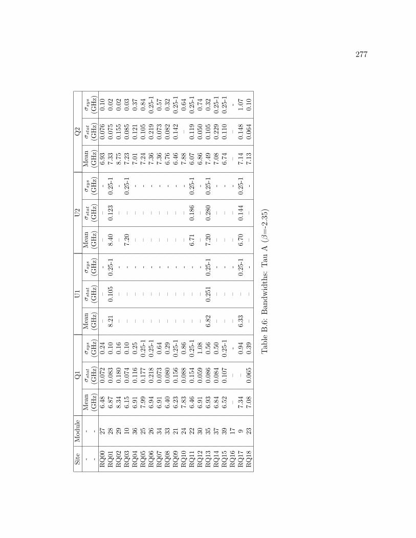
277
Site
Mod
ule
Q1
U1
U2
Q2
--
Mea
nσ
sta
tσ
sys
Mea
nσ
sta
tσ
sys
Mea
nσ
sta
tσ
sys
Mea
nσ
sta
tσ
sys
--
(GH
z)(G
Hz)
(GH
z)(G
Hz)
(GH
z)(G
Hz)
(GH
z)(G
Hz)
(GH
z)(G
Hz)
(GH
z)(G
Hz)
RQ
0027
6.48
0.07
20.
24–
–-
––
-6.
930.
076
0.10
RQ
0128
6.87
0.08
30.
108.
210.
105
0.25
-18.
400.
123
0.25
-17.
330.
075
0.02
RQ
0229
8.34
0.18
00.
16–
–-
––
-8.
750.
155
0.02
RQ
0310
6.15
0.07
40.
10–
–-
7.20
–0.
25-1
7.23
0.08
50.
03R
Q04
366.
910.
116
0.25
––
-–
–-
7.01
0.12
10.
37R
Q05
257.
990.
177
0.25
-1–
–-
––
-7.
240.
105
0.84
RQ
0626
6.94
0.21
80.
25-1
––
-–
–-
7.36
0.21
90.
25-1
RQ
0734
6.91
0.07
30.
64–
–-
––
-7.
360.
073
0.57
RQ
0833
6.40
0.08
00.
29–
–-
––
-6.
760.
082
0.32
RQ
0921
6.23
0.15
60.
25-1
––
-–
–-
6.46
0.14
20.
25-1
RQ
1024
7.83
0.08
80.
86–
–-
––
-7.
88–
0.64
RQ
1122
6.46
0.15
40.
25-1
––
-6.
710.
186
0.25
-16.
070.
119
0.25
-1R
Q12
306.
910.
059
1.08
––
-–
–-
6.86
0.05
00.
74R
Q13
356.
930.
086
0.56
6.82
0.25
10.
25-1
7.20
0.28
00.
25-1
7.49
0.10
50.
32R
Q14
376.
840.
084
0.50
––
-–
–-
7.08
0.22
90.
25-1
RQ
1539
6.52
0.10
70.
25-1
––
-–
–-
6.74
0.11
00.
25-1
RQ
1617
––
-–
–-
––
-–
–-
RQ
179
7.34
–0.
946.
33–
0.25
-16.
700.
144
0.25
-17.
140.
148
1.07
RQ
1823
7.08
0.06
50.
39–
–-
––
-7.
130.
064
0.10
Tab
leB
.6:
Ban
dw
idth
s:Tau
A(β
=-2
.35)
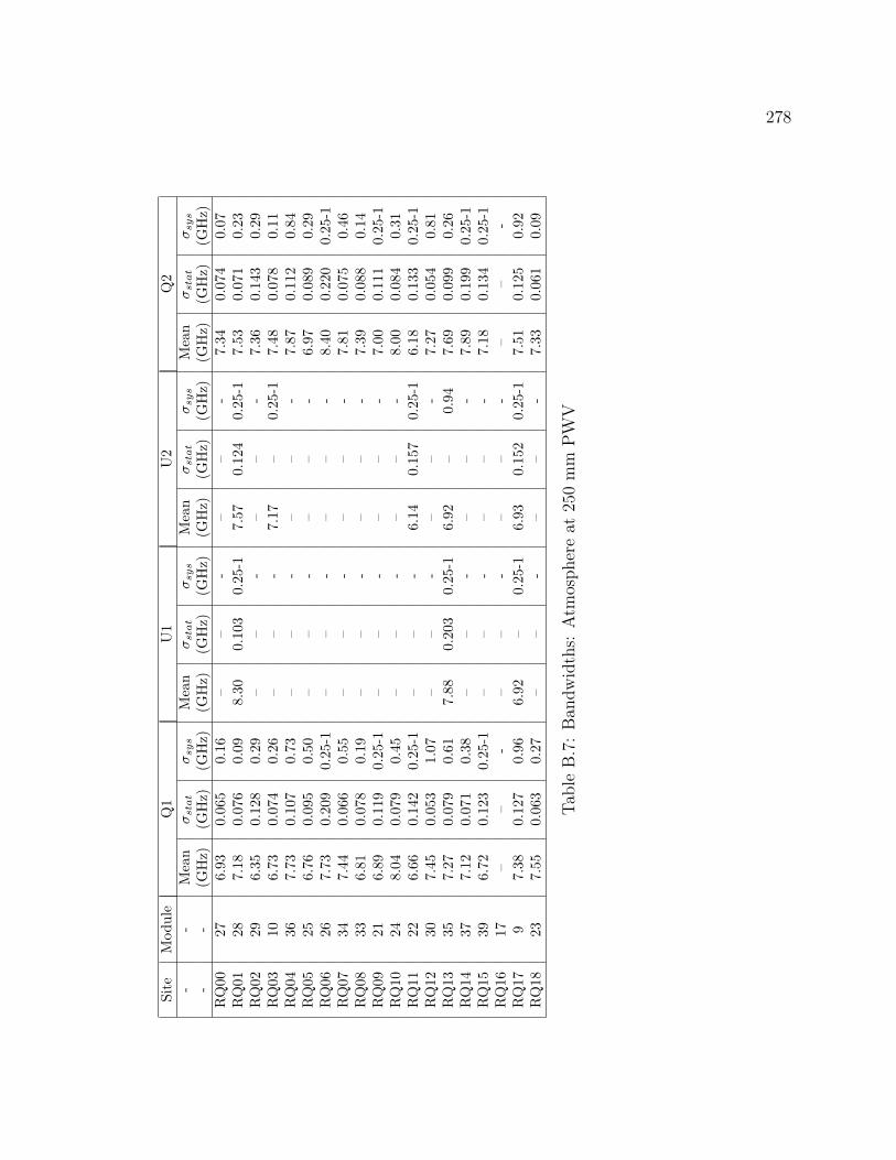
278
Site
Mod
ule
Q1
U1
U2
Q2
--
Mea
nσ
sta
tσ
sys
Mea
nσ
sta
tσ
sys
Mea
nσ
sta
tσ
sys
Mea
nσ
sta
tσ
sys
--
(GH
z)(G
Hz)
(GH
z)(G
Hz)
(GH
z)(G
Hz)
(GH
z)(G
Hz)
(GH
z)(G
Hz)
(GH
z)(G
Hz)
RQ
0027
6.93
0.06
50.
16–
–-
––
-7.
340.
074
0.07
RQ
0128
7.18
0.07
60.
098.
300.
103
0.25
-17.
570.
124
0.25
-17.
530.
071
0.23
RQ
0229
6.35
0.12
80.
29–
–-
––
-7.
360.
143
0.29
RQ
0310
6.73
0.07
40.
26–
–-
7.17
–0.
25-1
7.48
0.07
80.
11R
Q04
367.
730.
107
0.73
––
-–
–-
7.87
0.11
20.
84R
Q05
256.
760.
095
0.50
––
-–
–-
6.97
0.08
90.
29R
Q06
267.
730.
209
0.25
-1–
–-
––
-8.
400.
220
0.25
-1R
Q07
347.
440.
066
0.55
––
-–
–-
7.81
0.07
50.
46R
Q08
336.
810.
078
0.19
––
-–
–-
7.39
0.08
80.
14R
Q09
216.
890.
119
0.25
-1–
–-
––
-7.
000.
111
0.25
-1R
Q10
248.
040.
079
0.45
––
-–
–-
8.00
0.08
40.
31R
Q11
226.
660.
142
0.25
-1–
–-
6.14
0.15
70.
25-1
6.18
0.13
30.
25-1
RQ
1230
7.45
0.05
31.
07–
–-
––
-7.
270.
054
0.81
RQ
1335
7.27
0.07
90.
617.
880.
203
0.25
-16.
92–
0.94
7.69
0.09
90.
26R
Q14
377.
120.
071
0.38
––
-–
–-
7.89
0.19
90.
25-1
RQ
1539
6.72
0.12
30.
25-1
––
-–
–-
7.18
0.13
40.
25-1
RQ
1617
––
-–
–-
––
-–
–-
RQ
179
7.38
0.12
70.
966.
92–
0.25
-16.
930.
152
0.25
-17.
510.
125
0.92
RQ
1823
7.55
0.06
30.
27–
–-
––
-7.
330.
061
0.09
Tab
leB
.7:
Ban
dw
idth
s:A
tmos
pher
eat
250
mm
PW
V
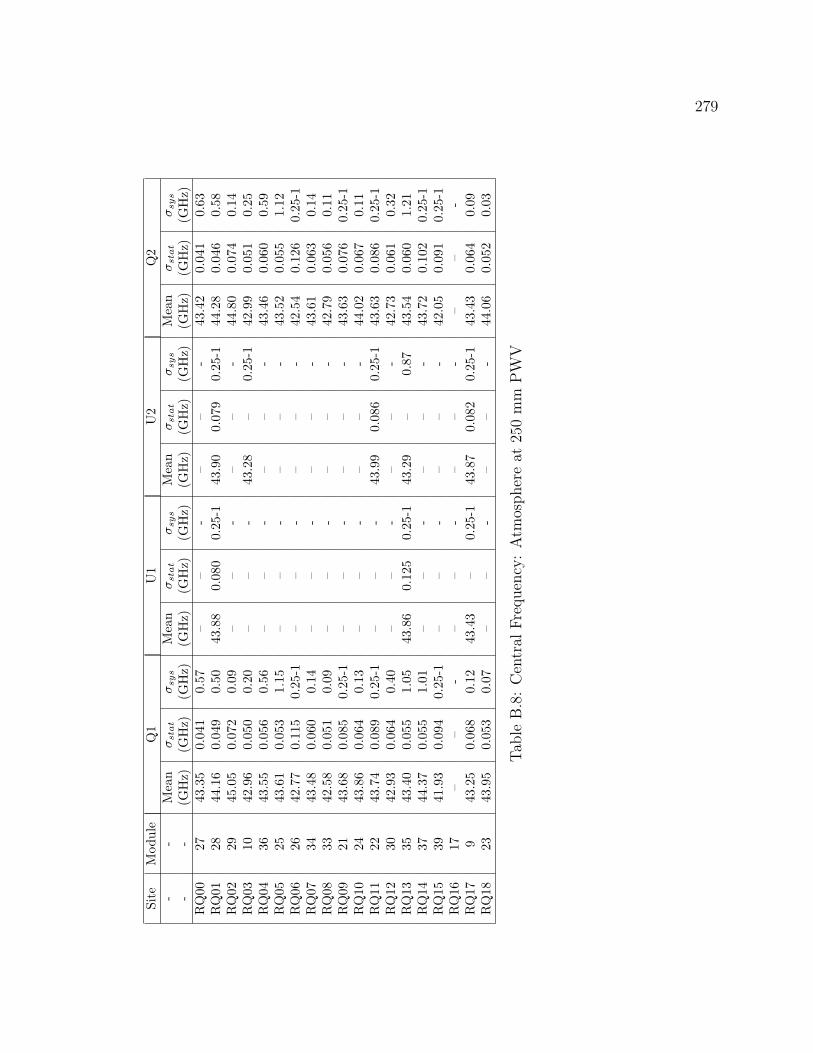
279
Site
Mod
ule
Q1
U1
U2
Q2
--
Mea
nσ
sta
tσ
sys
Mea
nσ
sta
tσ
sys
Mea
nσ
sta
tσ
sys
Mea
nσ
sta
tσ
sys
--
(GH
z)(G
Hz)
(GH
z)(G
Hz)
(GH
z)(G
Hz)
(GH
z)(G
Hz)
(GH
z)(G
Hz)
(GH
z)(G
Hz)
RQ
0027
43.3
50.
041
0.57
––
-–
–-
43.4
20.
041
0.63
RQ
0128
44.1
60.
049
0.50
43.8
80.
080
0.25
-143
.90
0.07
90.
25-1
44.2
80.
046
0.58
RQ
0229
45.0
50.
072
0.09
––
-–
–-
44.8
00.
074
0.14
RQ
0310
42.9
60.
050
0.20
––
-43
.28
–0.
25-1
42.9
90.
051
0.25
RQ
0436
43.5
50.
056
0.56
––
-–
–-
43.4
60.
060
0.59
RQ
0525
43.6
10.
053
1.15
––
-–
–-
43.5
20.
055
1.12
RQ
0626
42.7
70.
115
0.25
-1–
–-
––
-42
.54
0.12
60.
25-1
RQ
0734
43.4
80.
060
0.14
––
-–
–-
43.6
10.
063
0.14
RQ
0833
42.5
80.
051
0.09
––
-–
–-
42.7
90.
056
0.11
RQ
0921
43.6
80.
085
0.25
-1–
–-
––
-43
.63
0.07
60.
25-1
RQ
1024
43.8
60.
064
0.13
––
-–
–-
44.0
20.
067
0.11
RQ
1122
43.7
40.
089
0.25
-1–
–-
43.9
90.
086
0.25
-143
.63
0.08
60.
25-1
RQ
1230
42.9
30.
064
0.40
––
-–
–-
42.7
30.
061
0.32
RQ
1335
43.4
00.
055
1.05
43.8
60.
125
0.25
-143
.29
–0.
8743
.54
0.06
01.
21R
Q14
3744
.37
0.05
51.
01–
–-
––
-43
.72
0.10
20.
25-1
RQ
1539
41.9
30.
094
0.25
-1–
–-
––
-42
.05
0.09
10.
25-1
RQ
1617
––
-–
–-
––
-–
–-
RQ
179
43.2
50.
068
0.12
43.4
3–
0.25
-143
.87
0.08
20.
25-1
43.4
30.
064
0.09
RQ
1823
43.9
50.
053
0.07
––
-–
–-
44.0
60.
052
0.03
Tab
leB
.8:
Cen
tral
Fre
quen
cy:
Atm
ospher
eat
250
mm
PW
V
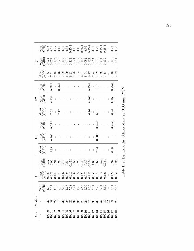
280
Site
Mod
ule
Q1
U1
U2
Q2
--
Mea
nσ
sta
tσ
sys
Mea
nσ
sta
tσ
sys
Mea
nσ
sta
tσ
sys
Mea
nσ
sta
tσ
sys
--
(GH
z)(G
Hz)
(GH
z)(G
Hz)
(GH
z)(G
Hz)
(GH
z)(G
Hz)
(GH
z)(G
Hz)
(GH
z)(G
Hz)
RQ
0027
6.90
0.06
50.
17–
–-
––
-7.
320.
074
0.08
RQ
0128
7.17
0.07
60.
098.
320.
102
0.25
-17.
630.
124
0.25
-17.
530.
071
0.21
RQ
0229
6.46
0.14
80.
31–
–-
––
-7.
480.
145
0.28
RQ
0310
6.68
0.07
30.
25–
–-
7.17
–0.
25-1
7.46
0.07
80.
11R
Q04
367.
690.
107
0.70
––
-–
–-
7.82
0.11
20.
81R
Q05
256.
780.
095
0.54
––
-–
–-
6.99
0.09
00.
33R
Q06
267.
680.
210
0.25
-1–
–-
––
-8.
330.
221
0.25
-1R
Q07
347.
410.
067
0.56
––
-–
–-
7.78
0.07
40.
47R
Q08
336.
760.
077
0.20
––
-–
–-
7.34
0.08
70.
15R
Q09
216.
850.
120
0.25
-1–
–-
––
-6.
970.
113
0.25
-1R
Q10
248.
050.
079
0.49
––
-–
–-
8.04
0.08
40.
36R
Q11
226.
650.
142
0.25
-1–
–-
6.16
0.16
60.
25-1
6.17
0.13
20.
25-1
RQ
1230
7.41
0.05
31.
08–
–-
––
-7.
240.
054
0.81
RQ
1335
7.26
0.07
90.
637.
840.
206
0.25
-16.
91–
0.96
7.69
0.09
90.
29R
Q14
377.
110.
072
0.32
––
-–
–-
7.86
0.20
10.
25-1
RQ
1539
6.69
0.12
10.
25-1
––
-–
–-
7.13
0.13
20.
25-1
RQ
1617
––
-–
–-
––
-–
–-
RQ
179
7.34
0.12
70.
976.
88–
0.25
-16.
940.
150
0.25
-17.
480.
126
0.93
RQ
1823
7.53
0.06
30.
28–
–-
––
-7.
320.
061
0.08
Tab
leB
.9:
Ban
dw
idth
s:A
tmos
pher
eat
5000
mm
PW
V
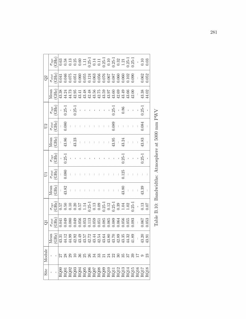
281
Site
Mod
ule
Q1
U1
U2
Q2
--
Mea
nσ
sta
tσ
sys
Mea
nσ
sta
tσ
sys
Mea
nσ
sta
tσ
sys
Mea
nσ
sta
tσ
sys
--
(GH
z)(G
Hz)
(GH
z)(G
Hz)
(GH
z)(G
Hz)
(GH
z)(G
Hz)
(GH
z)(G
Hz)
(GH
z)(G
Hz)
RQ
0027
43.3
10.
041
0.57
––
-–
–-
43.3
80.
041
0.63
RQ
0128
44.1
20.
049
0.50
43.8
20.
080
0.25
-143
.86
0.08
00.
25-1
44.2
40.
046
0.58
RQ
0229
44.9
90.
080
0.10
––
-–
–-
44.7
30.
075
0.13
RQ
0310
42.9
20.
049
0.20
––
-43
.23
–0.
25-1
42.9
50.
051
0.25
RQ
0436
43.4
90.
056
0.57
––
-–
–-
43.4
10.
060
0.60
RQ
0525
43.5
70.
053
1.14
––
-–
–-
43.4
80.
055
1.11
RQ
0626
42.7
20.
113
0.25
-1–
–-
––
-42
.48
0.12
40.
25-1
RQ
0734
43.4
40.
059
0.13
––
-–
–-
43.5
60.
063
0.14
RQ
0833
42.5
40.
051
0.09
––
-–
–-
42.7
50.
056
0.11
RQ
0921
43.6
40.
085
0.25
-1–
–-
––
-43
.59
0.07
60.
25-1
RQ
1024
43.8
00.
065
0.12
––
-–
–-
43.9
70.
067
0.10
RQ
1122
43.7
00.
089
0.25
-1–
–-
43.9
50.
089
0.25
-143
.60
0.08
70.
25-1
RQ
1230
42.8
90.
064
0.39
––
-–
–-
42.6
90.
060
0.32
RQ
1335
43.3
50.
056
1.04
43.8
00.
125
0.25
-143
.24
–0.
8643
.49
0.06
01.
21R
Q14
3744
.32
0.05
51.
02–
–-
––
-43
.66
0.10
20.
25-1
RQ
1539
41.8
90.
093
0.25
-1–
–-
––
-42
.00
0.09
00.
25-1
RQ
1617
––
-–
–-
––
-–
–-
RQ
179
43.2
00.
067
0.13
43.3
9–
0.25
-143
.83
0.08
40.
25-1
43.3
80.
062
0.10
RQ
1823
43.9
10.
053
0.07
––
-–
–-
44.0
20.
052
0.03
Tab
leB
.10:
Ban
dw
idth
s:A
tmos
pher
eat
5000
mm
PW
V
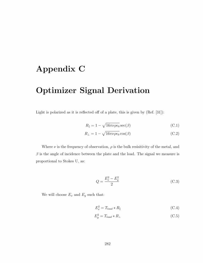
Appendix C
Optimizer Signal Derivation
Light is polarized as it is reflected off of a plate, this is given by (Ref. [31]):
R = 1−
16πνρ0 sec(β) (C.1)
R⊥ = 1−
16πνρ0 cos(β) (C.2)
Where ν is the frequency of observation, ρ is the bulk resisitivity of the metal, and
β is the angle of incidence between the plate and the load. The signal we measure is
proportional to Stokes U, as:
Q =E
2
x − E2
y
2(C.3)
We will choose Ex and Ey such that:
E2
x = Tload ∗R (C.4)
E2
y = Tload ∗R⊥ (C.5)
282
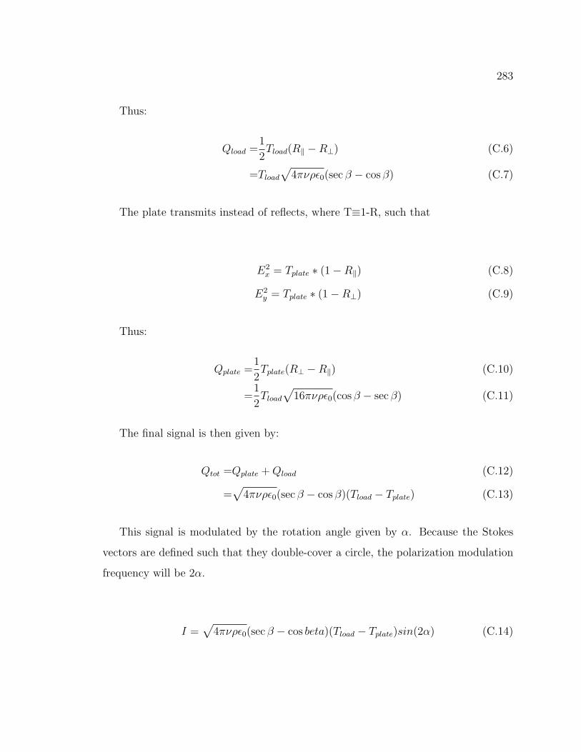
283
Thus:
Qload =1
2Tload(R −R⊥) (C.6)
=Tload
4πνρ0(sec β − cos β) (C.7)
The plate transmits instead of reflects, where T≡1-R, such that
E2
x = Tplate ∗ (1−R) (C.8)
E2
y = Tplate ∗ (1−R⊥) (C.9)
Thus:
Qplate =1
2Tplate(R⊥ −R) (C.10)
=1
2Tload
16πνρ0(cos β − sec β) (C.11)
The final signal is then given by:
Qtot =Qplate + Qload (C.12)
=
4πνρ0(sec β − cos β)(Tload − Tplate) (C.13)
This signal is modulated by the rotation angle given by α. Because the Stokes
vectors are defined such that they double-cover a circle, the polarization modulation
frequency will be 2α.
I =
4πνρ0(sec β − cos beta)(Tload − Tplate)sin(2α) (C.14)
Appendix D
Sensitivity Calculation
D.1 Array Sensitivity Computation
The RMS noise of a diode with intrinsic noise Trec, bandwidth ∆ν, integration time
τ , and target load temperature Tload is given by ([53]):
∆TRMS =Trec + Tload√
τ∆ν(D.1)
The sensitivity is given by:
S =Trec + Tload√
∆ν[
K√
Hz] (D.2)
This is also equivalent to the white noise floor σ (discussed in section 3.6) in units
of V/√
Hz) given the responsivity R (units of V/K):
S =σ
R[
K√
Hz] (D.3)
Typically these quantities are computed in units of seconds, the conversion is Hz/2
= 1/s.
284
285
D.1.1 Masking Factor
We mask the phase-switch transition region, masking 13% of the data. This results
in a masking factor of 0.87, which must be explicitly inserted into equation D.2 as a
factor which decreases τ . This factor is implicit in equation D.3 through the Fourier
transform of the noise (which is used to obtain the noise floor).
Typical values for diode sensitivity after including the masking factor are 1mK√
s.
D.1.2 Combining Diodes to Find Array Sensitivity
Sarray =
diode S
2
diode
N(D.4)
If all diodes have equal sensitivity, the sensitivity of the array will be Sarray =
Sdiode√N
. The array sensitivity while looking at a cryogenic load is 110µK√
s and
119µK√
s for equation D.2 and D.3, respectively.
D.1.3 Extrapolation for the Chilean Sky
We measure both Trec and σ while looking at a cryogenic load, however noise scales
with input load, so the noise measured while looking at the Chilean sky will be
larger than we would measure while looking at the Chilean sky. To extrapolate the
sensitivity values computed from cryogenic loads to the Chilean sky, we correct the
sensitivity by:
Trec + Tsky
Trec + Tcryogenic(D.5)
for both equation D.2 and D.3. We will assume a sky temperature of 11K with a
CMB temperature of 3K, giving a total sky temperature of 14K.
286
D.1.4 Rayleigh-Jeans Correction
The computation of noise (above) assumed that the power measured by the po-
larimeter is directly proportional to temperature. This approximation is valid at long
wavelengths, however it begins to break down when λ <1 cm.
The expression for the brightness of a thermal source is given by:
BPlanck(ν, T ) =2hν
3
c2
1
ehν/kT − 1(D.6)
where h is Planck’s constant, k is the Boltzmann constant, and c is the speed of
light. The linear approximation to this (hν kT ) is known as the Rayleigh-Jeans
law and has the form:
BRJ(ν, T ) =2ν3
kT
c3(D.7)
Such that the brightness temperature in the Rayleigh-Jeans approximation is given
by:
TB =BRJ(ν, T )c3
2ν3k(D.8)
Antenna noise temperature is defined in the Rayleigh-Jeans approximation. To ex-
press noise temperature in terms of thermodynamic units, we compare the brightness
BPlanck with BRJ , and make a distinction between the temperature in thermodynamic
units (Tθ) and in antenna noise temperature TA:
BPlanck = BRJ (D.9)
2hν3
c2
1
ehν/kTθ − 1=
2ν3kTA
c3(D.10)
TA =hν/k
ehν/kT − 1(D.11)
287
The correction from antenna noise temperature into thermodynamic units is then
given by:
Tθ
TA=
ehν/kTθ − 1
hν/kTθ(D.12)
This is noted in a variety of references, including Ref. [9]. The Q-band (40 GHz)
will have a correction factor of 1.45, the W-band (90 GHz) will have a correction
factor of 2.44 for a thermodynamic temperature Tθ = TCMB = 2.73K.
These corrections together give us an extrapolation for expected sensitivity to the
CMB given the Chilean sky temperature of 14K: 56µK√
s and 68µK√
s for equa-
tion D.2 and D.3, respectively.
Related Documents


