[17:36 2006/4/19 Chap-01.tex] MANIKTALA: Switching Power Supplies A to Z Page: 1 1–60 CHAPTER 1 The Principles of Switching Power Conversion

Welcome message from author
This document is posted to help you gain knowledge. Please leave a comment to let me know what you think about it! Share it to your friends and learn new things together.
Transcript
Typeset by: CEPHA Imaging Pvt. Ltd., INDIA
[17:36 2006/4/19 Chap-01.tex] MANIKTALA: Switching Power Supplies A to Z Page: 1 1–60
C H A P T E R
1
The Principles of SwitchingPower Conversion

Typeset by: CEPHA Imaging Pvt. Ltd., INDIA
[17:36 2006/4/19 Chap-01.tex] MANIKTALA: Switching Power Supplies A to Z Page: 2 1–60
Typeset by: CEPHA Imaging Pvt. Ltd., INDIA
[17:36 2006/4/19 Chap-01.tex] MANIKTALA: Switching Power Supplies A to Z Page: 3 1–60
C H A P T E R 1The Principles of Switching Power Conversion
IntroductionImagine we are at some busy “metro” terminus one evening at peak hour. Almost instantly,thousands of commuters swarm the station trying to make their way home. Of course there isno train big enough to carry all of them simultaneously. So, what do we do? Simple! Wesplit this sea of humanity into several trainloads — and move them out in rapid succession.Many of these outbound passengers will later transfer to alternative forms of transport. Sofor example, trainloads may turn into bus-loads or taxi-loads, and so on. But eventually, allthese “packets” will merge once again, and a throng will be seen, exiting at the destination.
Switching power conversion is remarkably similar to a mass transit system. The difference isthat instead of people, it is energy that gets transferred from one level to another. So wedraw energy continuously from an ‘input source’, chop this incoming stream into packets bymeans of a ‘switch’ (a transistor), and then transfer it with the help of components (inductorsand capacitors), that are able to accommodate these energy packets and exchange themamong themselves as required. Finally, we make all these packets merge again, and therebyget a smooth and steady flow of energy into the output.
So, in either of the cases above (energy or people), from the viewpoint of an observer, astream will be seen entering, and a similar one exiting. But at an intermediate stage, thetransference is accomplished by breaking up this stream into more manageable packets.
Looking more closely at the train station analogy, we also realize that to be able to transfer agiven number of passengers in a given time (note that in electrical engineering, energytransferred in unit time is ‘power’) — either we need bigger trains with departure timesspaced relatively far apart OR several smaller trains leaving in rapid succession. Therefore,it should come as no surprise, that in switching power conversion, we always try to switch athigh frequencies. The primary purpose for that is to reduce the size of the energy packets,and thereby also the size of the components required to store and transport them.
Power supplies that use this principle are called ‘switching power supplies’ or ‘switchingpower converters’.
‘Dc-dc converters’ are the basic building blocks of modern high-frequency switching powersupplies. As their name suggests, they ‘convert’ an available dc (direct current) input voltagerail ‘VIN’, to another more desirable or usable dc output voltage level ‘VO’. ‘Ac-dc
3
Typeset by: CEPHA Imaging Pvt. Ltd., INDIA
[17:36 2006/4/19 Chap-01.tex] MANIKTALA: Switching Power Supplies A to Z Page: 4 1–60
Chapter 1
Primary Side Secondary Side
isolation boundary
Prim
ary Side C
ontrol Board
Input EM
I Filter
Bridge R
ectifier
Input (Bulk) C
apacitor
Sw
itch (on Heatsink)
Transform
er
Secondary S
ide Diodes
Output C
hoke
Output C
apacitors
Secondary S
ide Control B
oard
Optocouplers
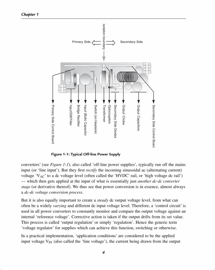
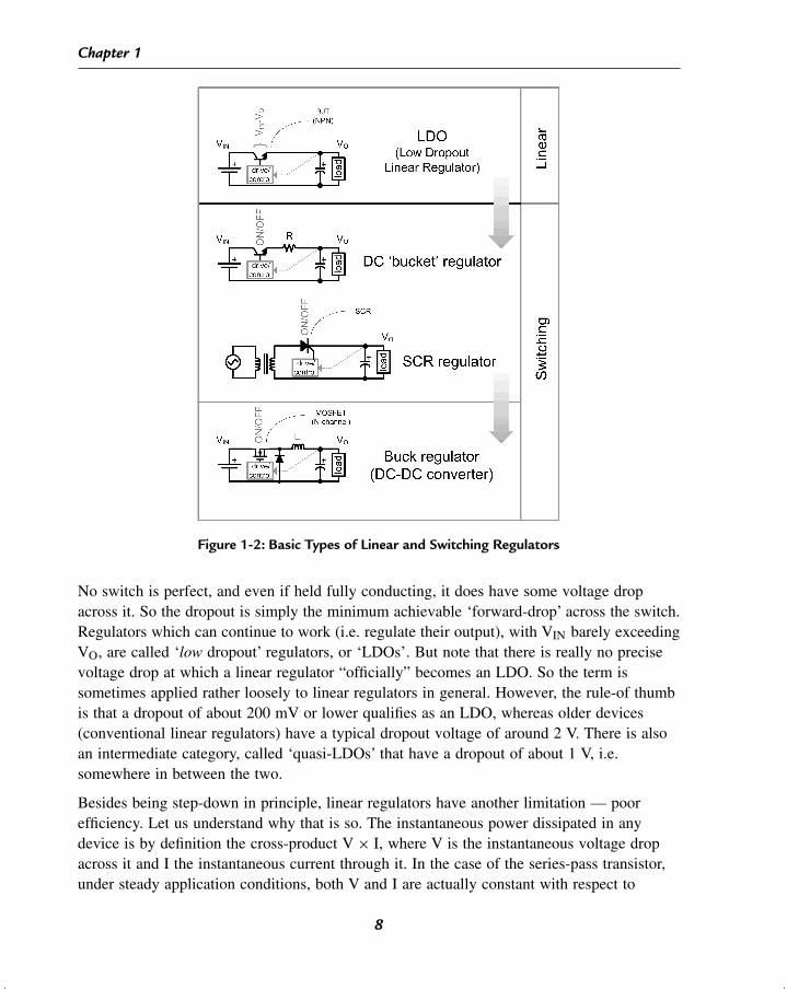
Figure 1-1: Typical Off-line Power Supply
converters’ (see Figure 1-1), also called ‘off-line power supplies’, typically run off the mainsinput (or ‘line input’). But they first rectify the incoming sinusoidal ac (alternating current)voltage ‘VAC’ to a dc voltage level (often called the ‘HVDC’ rail, or ‘high voltage dc rail’)— which then gets applied at the input of what is essentially just another dc-dc converterstage (or derivative thereof). We thus see that power conversion is in essence, almost alwaysa dc-dc voltage conversion process.
But it is also equally important to create a steady dc output voltage level, from what canoften be a widely varying and different dc input voltage level. Therefore, a ‘control circuit’ isused in all power converters to constantly monitor and compare the output voltage against aninternal ‘reference voltage’. Corrective action is taken if the output drifts from its set value.This process is called ‘output regulation’ or simply ‘regulation’. Hence the generic term‘voltage regulator’ for supplies which can achieve this function, switching or otherwise.
In a practical implementation, ‘application conditions’ are considered to be the appliedinput voltage VIN (also called the ‘line voltage’), the current being drawn from the output
4
Typeset by: CEPHA Imaging Pvt. Ltd., INDIA
[17:36 2006/4/19 Chap-01.tex] MANIKTALA: Switching Power Supplies A to Z Page: 5 1–60
The Principles of Switching Power Conversion
i.e. IO (the ‘load current’) and the set output voltage VO. Temperature is also an applicationcondition, but we will ignore it for now, since its effect on the system is usually not sodramatic. Therefore, for a given output voltage, there are two specific application conditionswhose variations can cause the output voltage to be immediately impacted (were it not forthe control circuit). Maintaining the output voltage steady when VIN varies over its statedoperating range VINMIN to VINMAX (minimum input to maximum input), is called ‘lineregulation’. Whereas maintaining regulation when IO varies over its operating range IOMIN toIOMAX (minimum to maximum load), is referred to as ‘load regulation’. Of course, nothingis ever “perfect”, so nor is the regulation. Therefore, despite the correction, there is a smallbut measurable change in the output voltage, which we call “∆VO” here. Note thatmathematically, line regulation is expressed as “∆VO/VO × 100% (implicitly implying itis over VINMIN to VINMAX)”. Load regulation is similarly “∆VO/VO × 100%” (from IOMIN
to IOMAX).
However, the rate at which the output can be corrected by the power supply (under suddenchanges in line and load) is also important — since no physical process is “instantaneous”either. So the property of any converter to provide quick regulation (correction) underexternal disturbances is referred to as its ‘loop response’. Clearly, the loop response is asbefore, a combination of its ‘step-load response’ and its ‘line transient response’.
As we move on, we will first introduce the reader to some of the most basic terminology ofpower conversion and its key concerns. Later, we will progress towards understanding thebehavior of the most vital component of power conversion — the inductor. It is thiscomponent that even some relatively experienced power designers still have trouble with!Clearly, real progress in any area cannot occur without a clear understanding of thecomponents and basic concepts involved. Therefore, only after understanding the inductorwell, will we go on to demonstrate that switching converters themselves are not all thatmysterious either — in fact they evolve quite naturally out of our newly acquiredunderstanding of the inductor.
Overview and Basic TerminologyEfficiency
Any regulator carries out the process of power conversion with an ‘efficiency’, defined as
η = PO
PIN
where PO is the ‘output power’, equal to
PO = VO × IO
5
Typeset by: CEPHA Imaging Pvt. Ltd., INDIA
[17:36 2006/4/19 Chap-01.tex] MANIKTALA: Switching Power Supplies A to Z Page: 6 1–60
Chapter 1
and PIN is the ‘input power’, equal to
PIN = VIN × IIN
Here, IIN is the average or dc current being drawn from the source.
Ideally we want η = 1, and that would represent a “perfect” conversion efficiency of 100%But in a real converter, i.e. with η < 1, the difference ‘PIN − PO’ is simply the wasted power“Ploss”, or ‘dissipation’ (occurring within the converter itself). By simple manipulation we get
Ploss = PIN − PO
Ploss = PO
η− PO
Ploss = PO ×(
1 − η
η
)
This is the loss expressed in terms of the output power. In terms of the input power wewould similarly get
Ploss = PIN × (1 − η
)
The loss manifests itself as heat in the converter, which in turn causes a certain measurable‘temperature rise’ ∆T over the surrounding ‘room temperature’ (or ‘ambient temperature’).Note that high temperatures affect the reliability of all systems — the rule-of-thumb beingthat every 10C rise causes the failure rate to double. Therefore, part of our skill as designersis to reduce this temperature rise, and thereby also achieve higher efficiencies.
Coming to the input current (drawn by the converter), for the hypothetical case of 100%efficiency, we get
IIN_ideal = IO ×(
VO
VIN
)
So, in a real converter, the input current increases from its “ideal” value by the factor 1/η.
IIN_measured = 1
η× IIN_ideal
Therefore, if we can achieve a high efficiency, the current drawn from the input (keepingapplication conditions unchanged) will decrease — but only up to a point. The inputcurrent clearly cannot fall below the “brickwall” that is “IIN_ideal”. Because this current is
6
Typeset by: CEPHA Imaging Pvt. Ltd., INDIA
[17:36 2006/4/19 Chap-01.tex] MANIKTALA: Switching Power Supplies A to Z Page: 7 1–60
The Principles of Switching Power Conversion
equal to PO/VIN — i.e. related only to the ‘useful power’ PO, delivered by the power supply,which we are assuming has not changed.
Further, since
VO × IO = VIN × IIN_ideal
by simple algebra, the dissipation in the power supply (energy lost per second as heat) canalso be written as
Ploss = VIN × (IIN_measured − IIN_ideal
)
This form of the dissipation equation indicates a little more explicitly how additional energy(more input current for a given input voltage) is pushed into the input terminals of the powersupply by the applied dc source — to compensate for the wasted energy inside the powersupply — even as the converter continues to provide the useful energy PO being constantlydemanded by the load.
A modern switching power supply’s efficiency can typically range from 65 to 95% — thatfigure being considered attractive enough to have taken switchers to the level of interest theyarouse today, and their consequent wide application. Traditional regulators (like the ‘linearregulator’) provide much poorer efficiencies — and that is the main reason why they areslowly but surely getting replaced by switching regulators.
Linear Regulators
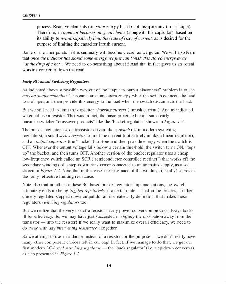
‘Linear regulators’, equivalently called ‘series-pass regulators’, or simply ‘series regulators’,also produce a regulated dc output rail from an input rail. But they do this by placing atransistor in series between the input and output. Further, this ‘series-pass transistor’(or ‘pass-transistor’) is operated in the linear region of its voltage-current characteristics —thus acting like a variable resistance of sorts. As shown in the uppermost schematic ofFigure 1-2, this transistor is made to literally “drop” (abandon) the unwanted or “excess”voltage across itself.
The excess voltage is clearly just the difference ‘VIN − VO’ — and this term is commonlycalled the ‘headroom’ of the linear regulator. We can see that the headroom needs to be apositive number always, thus implying VO < VIN. Therefore, linear regulators are inprinciple, always ‘step-down’ in nature — that being their most obvious limitation.
In some applications (e.g. battery powered portable electronic equipment), we may want theoutput rail to remain well-regulated even if the input voltage dips very low — say down towithin 0.6 V or less of the set output level VO. In such cases, the minimum possibleheadroom (or ‘dropout’) achievable by the linear regulator stage may become an issue.
7
Typeset by: CEPHA Imaging Pvt. Ltd., INDIA
[17:36 2006/4/19 Chap-01.tex] MANIKTALA: Switching Power Supplies A to Z Page: 8 1–60
Chapter 1
Figure 1-2: Basic Types of Linear and Switching Regulators
No switch is perfect, and even if held fully conducting, it does have some voltage dropacross it. So the dropout is simply the minimum achievable ‘forward-drop’ across the switch.Regulators which can continue to work (i.e. regulate their output), with VIN barely exceedingVO, are called ‘low dropout’ regulators, or ‘LDOs’. But note that there is really no precisevoltage drop at which a linear regulator “officially” becomes an LDO. So the term issometimes applied rather loosely to linear regulators in general. However, the rule-of thumbis that a dropout of about 200 mV or lower qualifies as an LDO, whereas older devices(conventional linear regulators) have a typical dropout voltage of around 2 V. There is alsoan intermediate category, called ‘quasi-LDOs’ that have a dropout of about 1 V, i.e.somewhere in between the two.
Besides being step-down in principle, linear regulators have another limitation — poorefficiency. Let us understand why that is so. The instantaneous power dissipated in anydevice is by definition the cross-product V × I, where V is the instantaneous voltage dropacross it and I the instantaneous current through it. In the case of the series-pass transistor,under steady application conditions, both V and I are actually constant with respect to
8
Typeset by: CEPHA Imaging Pvt. Ltd., INDIA
[17:36 2006/4/19 Chap-01.tex] MANIKTALA: Switching Power Supplies A to Z Page: 9 1–60
The Principles of Switching Power Conversion
time — V in this case being the headroom VIN − VO, and I the load current IO (since thetransistor is always in series with the load). So we see that the V × I dissipation term forlinear regulators can under certain conditions, become a significant proportion of the usefuloutput power PO. And that simply spells “poor efficiency”! Further, if we stare hard at theequations, we will realize there is also nothing we can do about it — how can we possiblyargue against something as basic as V × I? For example, if the input is 12 V, and the outputis 5 V, then at a load current of 100 mA, the dissipation in the regulator is necessarily∆V × IO = (12 − 5) V × 100 mA = 700 mW. The useful (output) power is howeverVO × IO = 5 V × 100 mA = 500 mW. Therefore, the efficiency is PO/PIN = 500/(700 +500) = 41.6%. What can we do about that?!
On the positive side, linear regulators are very “quiet” — exhibiting none of the noise andEMI (electromagnetic interference) that have unfortunately become a “signature” or“trademark” of modern switching regulators. Switching regulators need filters — usuallyboth at the input and the output, to quell some of this noise, which can interfere with othergadgets in the vicinity, possibly causing them to malfunction. Note that sometimes, the usualinput/output capacitors of the converter may themselves serve the purpose, especially whenwe are dealing with ‘low-power’ (and ‘low-voltage’) applications. But in general, we mayrequire filter stages containing both inductors and capacitors. Sometimes these stages mayneed to be cascaded to provide even greater noise attenuation.
Achieving High Efficiency through Switching
Why are switchers so much more efficient than “linears”?
As their name indicates, in a switching regulator, the series transistor is not held in aperpetual partially conducting (and therefore dissipative) mode — but is instead switchedrepetitively. So there are only two states possible — either the switch is held ‘ON’ (fullyconducting) or it is ‘OFF’ (fully non-conducting) — there is no “middle ground” (at least notin principle). When the transistor is ON, there is (ideally) zero voltage across it (V = 0), andwhen it is OFF we have zero current through it (I = 0). So it is clear that the cross-product‘V × I’ is also zero for either of the two states. And that simply implies zero ‘switchdissipation’ at all times. Of course this too represents an impractical or “ideal” case. Realswitches do dissipate. One reason for that they are never either fully ON nor fully OFF. Evenwhen they are supposedly ON, they have a small voltage drop across them, and when theyare supposedly “OFF”, a small current still flows through them. Further, no device switches“instantly” either — there is always definable period in which the device is transitingbetween states. During this interval too, V × I is not zero, and some additional dissipationoccurs.
We may have noticed that in most introductory texts on switching power conversion, theswitch is shown as a mechanical device — with contacts that simply open (“switch OFF”)
9
Typeset by: CEPHA Imaging Pvt. Ltd., INDIA
[17:36 2006/4/19 Chap-01.tex] MANIKTALA: Switching Power Supplies A to Z Page: 10 1–60
Chapter 1
or close (“switch ON”). So a mechanical device comes very close to our definition of a“perfect switch” — and that is the reason why it is often the vehicle of choice to present themost basic principles of power conversion. But one obvious problem with actually using amechanical switch in any practical converter is that such switches can wear out and fail overa relatively short period of time. So in practice, we always prefer to use a semiconductordevice (e.g. a transistor) as the switching element. As expected, that greatly enhances the lifeand reliability of the converter. But the most important advantage is that since asemiconductor switch has none of the mechanical “inertia” associated with a mechanicaldevice, it gives us the ability to switch repetitively between the ON and OFF states — anddo so very fast. We have already realized that that will lead to smaller components ingeneral.
We should be clear that the phrase “switching fast”, or “high switching speed”, has slightlyvarying connotations, even within the area of switching power conversion. When it isapplied to the overall circuit, it refers to the frequency at which we are repeatedly switching— ON OFF ON OFF and so on. This is the converter’s basic switching frequency ‘f’ (in Hz).But when the same term is applied specifically to the switching element or device, it refers tothe time spent transiting between its two states (i.e. from ON to OFF and OFF to ON), and istypically expressed in ‘ns’ (nanoseconds). Of course this transition interval is then ratherimplicitly and intuitively being compared to the total ‘time period’ T (where T = 1/f ), andtherefore to the switching frequency — though we should be clear there is no directrelationship between the transition time and the switching frequency.
We will learn shortly that the ability to crossover (i.e. transit) quickly between switchingstates is in fact rather crucial. Yes, up to a point, the switching speed is almost completelydetermined by how “strong” and effective we can make our external ‘drive circuit’. Butultimately, the speed becomes limited purely by the device and its technology — an “inertia”of sorts at an electrical level.
Basic Types of Semiconductor Switches
Historically, most power supplies used the ‘bjt’ (bipolar junction transistor) shown inFigure 1-2. It is admittedly a rather slow device by modern standards. But it is still relativelycheap! In fact its ‘npn’ version is even cheaper, and therefore more popular than its ‘pnp’version. Modern switching supplies prefer to use a ‘mosfet’ (metal oxide semiconductor fieldeffect transistor), often simply called a ‘fet’ (see Figure 1-2 again). This modern high-speedswitching device also comes in several “flavors” — the most commonly used ones being then-channel and p-channel types (both usually being the ‘enhancement mode’ variety). Then-channel mosfet happens to be the favorite in terms of cost-effectiveness and performance,for most applications. However, sometimes, p-channel devices may be preferred for variousreasons — mainly because they usually require simpler drive circuits.
10
Typeset by: CEPHA Imaging Pvt. Ltd., INDIA
[17:36 2006/4/19 Chap-01.tex] MANIKTALA: Switching Power Supplies A to Z Page: 11 1–60
The Principles of Switching Power Conversion
Despite the steady course of history in favor of mosfets in general, there still remain somearguments for continuing to prefer bjts in certain applications. Some points to consider anddebate here are:
a) It is often said that it is easier to drive a mosfet than a bjt. In a bjt we do need alarge drive current (injected into its ‘Base’ terminal) — to turn it ON. We also needto keep injecting Base current to keep it in that state. On the other hand, a mosfetis considered easier to drive. In theory, we just have to apply a certain voltage at its‘Gate’ terminal to turn it ON, and also keep it that way. Therefore, a mosfet is called a‘voltage-controlled’ device, whereas a bjt is considered a ‘current controlled’ device.However, in reality, a modern mosfet needs a certain amount of Gate current duringthe time it is in transit (ON to OFF and OFF to ON). Further, to make it change statefast, we may in fact need to push in (or pull) out a lot of current (typically 1 to 2 A).
b) The drive requirements of a bjt may actually turn out easier to implement in manycases. The reason for that is, to turn an npn bjt ON for example, its Gate has to betaken only about 0.8 V above its Emitter (and can even be tied directly to its Collectoron occasion). Whereas, in an n-channel mosfet, its Gate has to be taken several voltshigher than its Source. Therefore, in certain types of dc-dc converters, when using ann-channel mosfet, it can be shown that we need a ‘drive rail’ that is significantly higherthan the (available) input rail VIN. And how else can we hope to have such a railexcept by a circuit that can somehow manage to “push” or “pump” the input voltageto a higher level? When thus implemented, such a rail is called the ‘bootstrap’ rail.
Note: The most obvious implementation of a ‘bootstrap circuit’ may just consist of a smallcapacitor that gets charged by the input source (through a small signal diode) whenever the switchturns OFF. Thereafter, when the switch turns ON, we know that certain voltage nodes in the powersupply suddenly “flip” whenever the switch changes state. But since the ‘bootstrap capacitor’continues to hold on to its acquired voltage (and charge), it automatically pumps the bootstrap rail toa level higher than the input rail, as desired. This rail then helps drive the mosfet properly under allconditions.
c) The main advantage of bjts is that they are known to generate significantly less EMIand ‘noise and ripple’ than mosfets. That ironically is a positive outcome of theirslower switching speed!
d) Bjts are also often better suited for high-current applications — because their ‘forwarddrop’ (on-state voltage drop) is relatively constant, even for very high switch currents.This leads to significantly lower ‘switch dissipation’, more so when the switchingfrequencies are not too high. On the contrary, in a mosfet, the forward drop is almostproportional to the current passing through it — so its dissipation can becomesignificant at high loads. Luckily, since it also switches faster (lower transitiontimes), it usually more than makes up, and so in fact becomes much better in termsof the overall loss — more so when operated at very high switching frequencies.
11
Typeset by: CEPHA Imaging Pvt. Ltd., INDIA
[17:36 2006/4/19 Chap-01.tex] MANIKTALA: Switching Power Supplies A to Z Page: 12 1–60
Chapter 1
Note: In an effort to combine the “best of both worlds”, a “combo” device called the ‘IGBT’(insulated gate bipolar transistor) is also often used nowadays. It is driven like a mosfet(voltage-controlled), but behaves like a bjt in other ways (the forward drop and switchingspeed). It too is therefore suited mainly for low-frequency and high-current applications, but isconsidered easier to drive than a bjt.
Semiconductor Switches Are Not “Perfect”
We mentioned that all semiconductor switches suffer losses. Despite their advantages, theyare certainly not the perfect or ideal switches we may have imagined them to be at first sight.
So for example, unlike a mechanical switch, in the case of a semiconductor device, we mayhave to account for the small but measurable ‘leakage current’ flowing through it when it isconsidered “fully OFF” (i.e. non-conducting). This gives us a dissipation term called the‘leakage loss’. Though, this term is usually not very significant, and can be ignored.However, there is a small but significant voltage drop (‘forward drop’) across thesemiconductor when it is considered “fully ON” (i.e. conducting) — and that gives us asignificant ‘conduction loss’ term. In addition, there is also a brief moment as we transitionbetween the two switching states, when the current and voltage in the switch need to slew upor down almost simultaneously to their new respective levels. So, during this ‘transition time’or ‘crossover time’, we neither have V = 0 nor I = 0 instantaneously, and therefore nor isV × I = 0. This therefore leads to some additional dissipation, and is called the ‘crossoverloss’ (or sometimes just ‘switching loss’). Eventually, we need to learn to minimize all suchloss terms if we want to improve the efficiency of our power supply.
However, we must remember that power supply design, is by its very nature, full of designtradeoffs and subtle compromises. For example, if we look around for a transistor witha very low forward voltage drop, possibly with the intent of minimizing the conduction loss,we usually end up with a device that also happens to transition more slowly — thus leadingto a higher crossover loss. There is also an overriding concern for cost that needs to beconstantly looked into, particularly in the commercial power supply arena. So, we should notunderestimate the importance of having an astute and seasoned engineer at the helm of affairs,one who can really grapple with the finer details of power supply design. As a corollary,neither can we probably ever hope to replace him or her (at least not entirely), by some smartautomatic test system, nor by any “expert design software” that we may have been dreaming of.
Achieving High Efficiency through the use of Reactive Components
We have seen that one reason why switching regulators have such a high efficiency isbecause they use a switch (rather than a transistor that “thinks” it is a resistor, as in an LDO).Another root cause of the high efficiency of modern switching power supplies is theireffective use of both capacitors and inductors.
12
Typeset by: CEPHA Imaging Pvt. Ltd., INDIA
[17:36 2006/4/19 Chap-01.tex] MANIKTALA: Switching Power Supplies A to Z Page: 13 1–60
The Principles of Switching Power Conversion
Capacitors and inductors are categorized as ‘reactive’ components because they have theunique ability of being able to store energy. However, that is why they cannot ever be madeto dissipate any energy either (at least not within themselves) — they just store any energy“thrown at them”! On the other hand, we know that ‘resistive’ components dissipate energy,but unfortunately, can’t store any!
A capacitor’s stored energy is called electrostatic, equal to ½ × C × V2 where C is the‘capacitance’ (in Farads), and V the voltage across the capacitor. Whereas an inductor storesmagnetic energy, equal to ½ × L × I2, L being the ‘inductance’ (in Henries) and I the currentpassing through it (at any given moment).
But we may well ask — despite the obvious efficiency concerns, do we really need reactivecomponents in principle? For example, we may have realized we don’t really need an inputor output capacitor for implementing a linear regulator — because the series-pass element isall that is required to block any excess voltage. For switching regulators however, thereasoning is rather different. This leads us to the general “logic of switching powerconversion” summarized below.
A transistor is needed to establish control on the output voltage, and thereby bring itinto regulation. The reason we switch it is as follows — dissipation in this controlelement is related to the product of the voltage across the control device and thecurrent through it, i.e. V × I. So if we make either V or I zero (or very small), wewill get zero (or very small) dissipation. By switching constantly between ON andOFF states, we can keep the switch dissipation down, but at the same time, bycontrolling the ratio of the ON and OFF intervals, we can regulate the output, basedon average energy flow considerations.
But whenever we switch the transistor, we effectively disconnect the input from theoutput (during either the ON or OFF state). However, the output (load) alwaysdemands a continuous flow of energy. Therefore we need to introduce energy storageelements somewhere inside the converter. In particular, we use output capacitors to“hold” the voltage steady across the load during the above-mentioned input-to-output“disconnect” interval.
But as soon as we put in a capacitor, we now also need to limit the inrush currentinto it — all capacitors connected directly across a dc source, will exhibit thisuncontrolled inrush — and that can’t be good either for noise, EMI or for efficiency.Of course we could simply opt for a resistor to subdue this inrush, and that in factwas the approach behind the early “bucket regulators” (Figure 1-2).
But unfortunately a resistor always dissipates — so what we may have saved interms of switch dissipation, may ultimately end up in the resistor! To maximize theoverall efficiency, we therefore need to use only reactive elements in the conversion
13
Typeset by: CEPHA Imaging Pvt. Ltd., INDIA
[17:36 2006/4/19 Chap-01.tex] MANIKTALA: Switching Power Supplies A to Z Page: 14 1–60
Chapter 1
process. Reactive elements can store energy but do not dissipate any (in principle).Therefore, an inductor becomes our final choice (alongwith the capacitor), based onits ability to non-dissipatively limit the (rate of rise) of current, as is desired for thepurpose of limiting the capacitor inrush current.
Some of the finer points in this summary will become clearer as we go on. We will also learnthat once the inductor has stored some energy, we just can’t wish this stored energy away“at the drop of a hat”. We need to do something about it! And that in fact gives us an actualworking converter down the road.
Early RC-based Switching Regulators
As indicated above, a possible way out of the “input-to-output disconnect” problem is to useonly an output capacitor. This can store some extra energy when the switch connects the loadto the input, and then provide this energy to the load when the switch disconnects the load.
But we still need to limit the capacitor charging current (‘inrush current’). And as indicated,we could use a resistor. That was in fact, the basic principle behind some earlylinear-to-switcher “crossover products” like the ‘bucket regulator’ shown in Figure 1-2.
The bucket regulator uses a transistor driven like a switch (as in modern switchingregulators), a small series resistor to limit the current (not entirely unlike a linear regulator),and an output capacitor (the “bucket”) to store and then provide energy when the switch isOFF. Whenever the output voltage falls below a certain threshold, the switch turns ON, “topsup” the bucket, and then turns OFF. Another version of the bucket regulator uses a cheaplow-frequency switch called an SCR (‘semiconductor controlled rectifier’) that works off thesecondary windings of a step-down transformer connected to an ac mains supply, as alsoshown in Figure 1-2. Note that in this case, the resistance of the windings (usually) serves asthe (only) effective limiting resistance.
Note also that in either of these RC-based bucket regulator implementations, the switchultimately ends up being toggled repetitively at a certain rate — and in the process, a rathercrudely regulated stepped down output dc rail is created. By definition, that makes theseregulators switching regulators too!
But we realize that the very use of a resistor in any power conversion process always bodesill for efficiency. So, we may have just succeeded in shifting the dissipation away from thetransistor — into the resistor! If we really want to maximize overall efficiency, we need todo away with any intervening resistance altogether.
So we attempt to use an inductor instead of a resistor for the purpose — we don’t really havemany other component choices left in our bag! In fact, if we manage to do that, we get ourfirst modern LC-based switching regulator — the ‘buck regulator’ (i.e. step-down converter),as also presented in Figure 1-2.
14
Typeset by: CEPHA Imaging Pvt. Ltd., INDIA
[17:36 2006/4/19 Chap-01.tex] MANIKTALA: Switching Power Supplies A to Z Page: 15 1–60
The Principles of Switching Power Conversion
LC-based Switching Regulators
Though the detailed functioning of the modern buck regulator of Figure 1-2 will beexplained a little later, we note that besides the obvious replacement of R with an L, it looksvery similar to the bucket regulator — except for a “mysterious” diode. The basic principlesof power conversion will in fact become clear only when we realize the purpose of this diode.This component goes by several names — ‘catch diode’, ‘freewheeling diode’,‘commutation diode’ ‘output diode’ to name a few! But its basic purpose is always the same— a purpose we will soon learn is intricately related to the behavior of the inductor itself.
Aside from the buck regulator, there are two other ways to implement the basic goal ofswitching power conversion (using both inductors and capacitors). Each of these leads to adistinct ‘topology’. So besides the buck (step-down), we also have the ‘boost’ (step-up), andthe ‘buck-boost’ (step-up or step-down). We will see that though all these are based on thesame underlying principles, they are set up to look and behave quite differently. As aprospective power supply designer, we really do need to learn and master each of themalmost on an individual basis. We must also keep in mind that in the process, our mentalpicture will usually need a drastic change as we go from one topology to another.
Note: There are some other capacitor-based possibilities — in particular ‘charge pumps’ — also called‘inductor-less switching regulators’. These are usually restricted to rather low powers and produce outputrails that are rather crudely regulated multiples of the input rail. In this book, we are going to ignore thesetypes altogether.
Then there are also some other types of LC-based possibilities — in particular the ‘resonant topologies’.Like conventional dc-dc converters, these also use both types of reactive components (L and C) along with aswitch. However, their basic principle of operation is very different. Without getting into their actual details,we note that these topologies do not maintain a constant switching frequency, which is something we usuallyrather strongly desire. From a practical standpoint, any switching topology with a variable switchingfrequency, can lead to an unpredictable and varying EMI spectrum and noise signature. To mitigate theseeffects, we may require rather complicated filters. For such reasons, resonant topologies have not reallyfound widespread acceptance in commercial designs, and so we too will largely ignore them from thispoint on.
The Role of Parasitics
In using conventional LC-based switching regulators, we may have noticed that theirconstituent inductors and capacitors do get fairly hot in most applications. But if, as we said,these components are reactive, why at all are they getting hot? We need to know why,because any source of heat impacts the overall efficiency! And efficiency is what modernswitching regulators are all about!
The heat arising from real-world reactive components can invariably be traced back todissipation occurring within the small ‘parasitic’ resistive elements, which always accompanyany such (reactive) component.
15
Typeset by: CEPHA Imaging Pvt. Ltd., INDIA
[17:36 2006/4/19 Chap-01.tex] MANIKTALA: Switching Power Supplies A to Z Page: 16 1–60
Chapter 1
For example, a real inductor has the basic property of inductance L, but it also has a certainnon-zero dc resistance (‘DCR’) term, mainly associated with the copper windings used.Similarly, any real capacitor has a capacitance C, but it also has a small equivalent seriesresistance (‘ESR’). Each of these terms produces ‘ohmic’ losses — that can all add up andbecome fairly significant.
As indicated previously, a real-world semiconductor switch can also be considered as havinga parasitic resistance “strapped” across it. This parallel resistor in effect “models” theleakage current path, and thus the ‘leakage loss’ term. Similarly, the forward drop across thedevice can also, in a sense, be thought of as a series parasitic resistance — leading to aconduction loss term.
But any real-world component also comes along with various reactive parasitics. Forexample an inductor can have a significant parasitic capacitance across its terminals —associated with electrostatic effects between the layers of its windings. A capacitor can alsohave an equivalent series inductance (‘ESL’) — coming from the small inductancesassociated with its leads, foil and terminations. Similarly, a mosfet also has various parasitics— for example the “unseen” capacitances present between each of its terminals (within thepackage). In fact, these mosfet parasitics play a major part in determining the limits of itsswitching speed (transition times).
In terms of dissipation, we understand that reactive parasitics certainly cannot dissipate heat— at least not within the parasitic element itself. But more often than not, these reactiveparasitics do manage to “dump” their stored energy (at specific moments during the switchingcycle) into a nearby resistive element — thus increasing the overall losses indirectly.
Therefore we see that to improve efficiency, we generally need to go about minimizing allsuch parasitics — resistive or reactive. We should not forget they are the very reason we arenot getting 100% efficiency from our converter in the first place. Of course, we have to learnto be able to do this optimization to within reasonable and cost-effective bounds, as dictatedby market compulsions and similar constraints.
But we should also bear in mind that nothing is so straightforward in power! So theseparasitic elements should not be considered entirely “useless” either. In fact they do play arather helpful and stabilizing role on occasion.
For example, if we short the outputs of a dc-dc converter, we know it is unable toregulate, however hard it tries. In this ‘fault condition’ (‘open-loop’), the momentary‘overload current’ within the circuit can be “tamed” (or mitigated) a great deal by thevery presence of certain identifiably “friendly” parasitics.
We will also learn that the so-called ‘voltage-mode control’ switching regulatorsactually rely on the ESR of the output capacitor for ensuring ‘loop stability’ — evenunder normal operation. As indicated previously, loop stability refers to the ability of
16
Typeset by: CEPHA Imaging Pvt. Ltd., INDIA
[17:36 2006/4/19 Chap-01.tex] MANIKTALA: Switching Power Supplies A to Z Page: 17 1–60
The Principles of Switching Power Conversion
a power supply to regulate its output quickly, when faced with sudden changes inline and load, without undue oscillations or ringing,
Certain other parasitics however may just prove to be a nuisance and some others a sheerbane. But their actual roles too may keep shifting, depending upon the prevailing conditionsin the converter. For example
A certain parasitic inductance may be quite helpful during the turn-on transition ofthe switch — by acting to limit any current spike trying to pass through the switch.But it can be harmful due to the high voltage spike it creates across the switch atturn-off (as it tries to release its stored magnetic energy).
On the other hand, a parasitic capacitance present across the switch for example,can be helpful at turn-off — but unhelpful at turn-on, as it tries to dump its storedelectrostatic energy inside the switch.
Note: We will find that during turn-off, the parasitic capacitance mentioned above, helps limit or‘clamp’ any potentially destructive voltage spikes appearing across the switch, by absorbing theenergy residing in that spike. It also helps decrease the crossover loss by slowing down the risingramp of voltage, and thereby reducing the V-I “overlap” (between the transiting V and I waveformsof the switch). However at turn-on, the same parasitic capacitance now has to discharge whateverenergy it acquired during the preceding turn-off transition — and that leads to a current spikeinside the switch. Note that this spike is externally “invisible” — apparent only by thehigher-than-expected switch dissipation, and the resulting higher-than-expected temperature.
Therefore, generally speaking, all parasitics constitute a somewhat “double-edged sword”,one that we just can’t afford to overlook for very long in practical power supply design.However, as we too will do in our some of discussions that follow, sometimes we canconsciously and selectively decide to ignore some of these second-order influences initially,just to build up basic concepts in power first. Because the truth is if we don’t do that, we justrun the risk of feeling quite overwhelmed, too early in the game!
Switching at High Frequencies
In attempting to generally reduce parasitics and their associated losses, we may notice thatthese are often dependent on various external factors — temperature for one. Some lossesincrease with temperature — for example the conduction loss in a mosfet. And some maydecrease — for example the conduction loss in a bjt (when operated with low currents).Another example of the latter type is the ESR-related loss of a typical aluminum electrolyticcapacitor, which also decreases with temperature. On the other hand, some losses may haverather “strange” shapes. For example, we could have an inverted “bell-shaped” curve —representing an optimum operating point somewhere between the two extremes. This is whatthe ‘core loss’ term of many modern ‘ferrite’ materials (used for inductor cores) looks like —it is at its minimum at around 80 to 90C, increasing on either side.
17
Typeset by: CEPHA Imaging Pvt. Ltd., INDIA
[17:36 2006/4/19 Chap-01.tex] MANIKTALA: Switching Power Supplies A to Z Page: 18 1–60
Chapter 1
From an overall perspective, it is hard to predict how all these variations with respect totemperature add up — and how the efficiency of the power supply is thereby affected bychanges in temperature.
Coming to the dependency of parasitics and related loss terms on frequency, we do find asomewhat clearer trend. In fact it is rather rare that to find any loss term that decreases athigher frequencies (though a notable exception to this is the loss in an aluminum electrolyticcapacitor — because its ESR decreases with frequency). Some of the loss terms arevirtually independent of frequency (e.g. conduction loss). And the remaining losses actuallyincrease almost proportionally to the switching frequency — e.g. the crossover loss. So ingeneral, we realize that lowering, not increasing the switching frequency would almostinvariably help improve efficiency.
There are other frequency-related issues too, besides efficiency. For example, we know thatswitching power supplies are inherently noisy, and generate a lot of EMI. By going to higherswitching frequencies, we may just be making matters worse. We can mentally visualize thateven the small connecting wires and ‘printed circuit board’ (PCB) traces become veryeffective antennas at high frequencies, and will likely spew out radiated EMI in everydirection.
This therefore begs the question: why at all are we face to face with a modern trend ofever-increasing switching frequencies? Why should we not decrease the switchingfrequency?
The first motivation towards higher switching frequencies was to simply take “the action”beyond audible human hearing range. Reactive components are prone to creating soundpressure waves for various reasons. So, the early LC-based switching power suppliesswitched at around 15–20 kHz, and were therefore barely audible, if at all.
The next impetus towards even higher switching frequencies came with the realization thatthe bulkiest component of a power supply, i.e. the inductor, could be almost proportionatelyreduced in size if the switching frequency was increased (everybody does seem to wantsmaller products, after all!). Therefore, successive generations of power converters movedupwards in almost arbitrary steps, typically 20 kHz, 50 kHz, 70 kHz, 100 kHz, 150 kHz,250 kHz, 300 kHz, 500 kHz, 1 MHz, 2 MHz and often even higher today. This actuallyhelped simultaneously reduce the size of the conducted EMI and input/output filteringcomponents — including the capacitors! High switching frequencies can also almostproportionately enhance the loop response of a power supply.
Therefore, we realize that the only thing holding us back at any moment of time from goingto even higher frequencies are the “switching losses”. This term is in fact rather broad —-encompassing all the losses that occur at the moment when we actually switch the transistor(i.e. from ON to OFF and/or OFF to ON). Clearly, the crossover loss mentioned earlier is
18
Typeset by: CEPHA Imaging Pvt. Ltd., INDIA
[17:36 2006/4/19 Chap-01.tex] MANIKTALA: Switching Power Supplies A to Z Page: 19 1–60
The Principles of Switching Power Conversion
just one of several possible switching loss terms. Note that it is easy to visualize why suchlosses are (usually) exactly proportional to the switching frequency — since energy is lostonly whenever we actually switch — therefore, the greater the number of times we do that(in a second), more is the energy lost (dissipation).
Finally, we also do need to learn how to manage whatever dissipation is still remaining inthe power supply. This is called ‘thermal management’, and that is one of the most importantgoals in any good power supply design. Let us look at that now.
Reliability, Life and Thermal Management
Thermal management basically just means trying to get the heat out from the power supplyand into the surroundings — thereby lowering the local temperatures at various pointsinside it. The most basic and obvious reason for doing this is to keep all the components towithin their maximum rated operating temperatures. But in fact, that is rarely enough. Wealways strive to reduce the temperatures even further, and every couple of degree Celsius(C) may well be worth fighting for.
The reliability ‘R’ of a power supply at any given moment of time is defined as R(t) = e−λt .So at time t = 0 (start of operational life), the reliability is considered to be at its maximumvalue of 1. Thereafter it decreases exponentially as time elapses. ‘λ‘ is the failure rate of apower supply, i.e. the number of supplies failing over a specified period of time. Anothercommonly used term is ‘MTBF’, or mean time between failures. This is the reciprocal of theoverall failure rate, i.e. λ = 1/MTBF. A typical commercial power supply will have anMTBF of between 100,000 hours to 500,000 hours — assuming it is being operated at afairly typical and benign ‘ambient temperature’ of around 25C.
Looking now at the variation of failure rate with respect to temperature, we come across thewell-known rule-of-thumb — failure rate doubles every 10C rise in temperature. If we applythis admittedly loose rule-of-thumb to each and every component used in the power supply,we see it must also hold for the entire power supply too — since the overall failure rate ofthe power supply is simply the sum of the failure rates of each component comprising it(λ = λ1 + λ2 + λ3 + . . . .). All this clearly gives us a good reason to try and reducetemperatures of all the components even further.
But aside from failure rate, which clearly applies to every component used in a powersupply, there are also certain ‘lifetime’ considerations that apply to specific components. The‘life’ of a component is stated to be the duration it can work for continuously, withoutdegrading beyond certain specified limits. At the end of this ‘useful life’, it is considered tohave become a ‘wearout failure’ — or simply put — it is “worn-out”. Note that this need notimply the component has failed “catastrophically” — more often than not, it may be just“out of spec”. The latter phrase simply means the component no longer provides the
19
Typeset by: CEPHA Imaging Pvt. Ltd., INDIA
[17:36 2006/4/19 Chap-01.tex] MANIKTALA: Switching Power Supplies A to Z Page: 20 1–60
Chapter 1
expected performance — as specified by the limits published in the electrical tables of itsdatasheet.
Note: Of course a datasheet can always be “massaged” to make the part look good in one way oranother — and that is the origin of a rather shady but widespread industry practice called “specmanship”.A good designer will therefore keep in mind that not all vendors’ datasheets are equal — even for what mayseem to be the same or equivalent part number at first sight.
As designers, it is important that we not only do our best to extend the ‘useful life’ of anysuch component, but also account upfront for its slow degradation over time. In effect, thatimplies that the power supply may initially perform better than its minimum specifications.Ultimately however, the worn-out component, especially if it is present at a critical location,could cause the entire power supply to “go out of spec”, and even fail catastrophically.
Luckily, most of the components used in a power supply have no meaningful or definablelifetime — at least not within the usual 5 to 10 years of useful life expected from mostelectronic products. We therefore usually don’t for example, talk in terms of an inductor ortransistor “degrading” (over a period of time) — though of course either of thesecomponents can certainly fail at any given moment, even under normal operation, asevidenced by their non-zero failure rates.
Note: Lifetime issues related to the materials used in the construction of a component can affect the life ofthe component indirectly. For example, if a semiconductor device is operated well beyond its usual maximumrating of 150C, its plastic package can exhibit wearout or degradation — even though nothing happens tothe semiconductor itself up to a much higher temperature. Subsequently, over a period of time, this degradedpackage can cause the junction to get severely affected by environmental factors, causing the device to failcatastrophically — usually taking the power supply (and system) with it too! In a similar manner, inductorsmade of ‘powdered iron’ type of core material are also known to degrade under extended periods of hightemperatures — and this can produce not only a failed inductor, but a failed power supply too.
A common example of lifetime considerations in a commercial power supply design comesfrom its use of aluminum electrolytic capacitors. Despite their great affordability andrespectable performance in many applications, such capacitors are a victim of wearout due tothe steady evaporation of their enclosed electrolyte over time. Extensive calculations areneeded to predict their internal temperature (‘core temperature’) and thereby estimate thetrue rate of evaporation and thereby extend the capacitor’s useful life. The rulerecommended for doing this life calculation is — the useful life of an aluminum electrolyticcapacitor halves every 10C rise in temperature. We can see that this relatively hard-and-fastrule is uncannily similar to the rule-of-thumb of failure rate. But that again, is just acoincidence, since life and failure rate are really two different issues altogether.
In either case, we can now clearly see that the way to extend life and improve reliability isto lower the temperatures of all the components in a power supply and also the ambienttemperature inside the enclosure of the power supply. This may also call out for abetter-ventilated enclosure (more air vents), more exposed copper on the PCB (printed
20
Typeset by: CEPHA Imaging Pvt. Ltd., INDIA
[17:36 2006/4/19 Chap-01.tex] MANIKTALA: Switching Power Supplies A to Z Page: 21 1–60
The Principles of Switching Power Conversion
circuit board), or say, even a built-in fan to push the hot air out. Though in the latter case,we now have to start worrying about both the failure rate and life of the fan itself!
Stress Derating
Temperature can ultimately be viewed as a ‘thermal stress’ — one that causes an increase infailure rate (and life if applicable). But how severe a stress really is, must naturally bejudged relative to the ‘ratings’ of the device. For example, most semiconductors are rated fora ‘maximum junction temperature’ of 150C. Therefore, keeping the junction no higher than105C in a given application, represents a stress reduction factor, or alternately — a‘temperature derating’ factor equal to 105/150 = 70%.
In general, ‘stress derating’ is the established technique used by good designers to diminishinternal stresses and thereby reduce the failure rate. Besides temperature, the failure rate(and life) of any component can also depend on the applied electrical stresses — voltage andcurrent. For example, a typical ‘voltage derating’ of 80% as applied to semiconductorsmeans that the worst-case operating voltage across the component never exceeds 80% of themaximum specified voltage rating of the device. Similarly, we can usually apply a typical‘current derating’ of 70–80% to most semiconductors.
The practice of derating also implies that we need to select our components judiciouslyduring the design phase itself — with well-considered and built-in operating margins. Andthough, as we know, some loss terms decrease with temperature, contemplating raising thetemperatures just to achieve better efficiency or performance, is clearly not the preferreddirection, because of the obvious impact on system reliability.
A good designer eventually learns to weigh reliability and life concerns against cost,performance, size, and so on.
Advances in Technology
But despite the best efforts of many a good power supply designer, certain sought afterimprovements may still have remained merely on our annual Christmas wish list! Luckily,there have been significant accompanying advances in the technology of the componentsavailable, to help enact out our goals. For example, the burning desire to reduce resistivelosses and simultaneously make designs suitable for high frequency operation has ushered insignificant improvements in terms of a whole new generation of high-frequency, low-ESRceramic and other specialty capacitors. We also have diodes with very low forward voltagedrops and ‘ultra-fast recovery’, much faster switches like the mosfet, and several newlow-loss ferrite material types for making the transformers and inductors.
Note: ‘Recovery’ refers to the ability of a diode to quickly change from a conducting state to anon-conducting (i.e. ‘blocking’) state as soon as the voltage across it reverses. Diodes which do this well are
21
Typeset by: CEPHA Imaging Pvt. Ltd., INDIA
[17:36 2006/4/19 Chap-01.tex] MANIKTALA: Switching Power Supplies A to Z Page: 22 1–60
Chapter 1
called ‘ultrafast diodes’. Note that the ‘Schottky diode’ is preferred in certain applications, because of its lowforward drop (∼0.5 V). In principle, it is also supposed to have zero recovery time. But unfortunately, it alsohas a comparatively higher parasitic ‘body capacitance’ (across itself), that in some ways tends to mimicconventional recovery phenomena. Note that it also has a higher leakage current and is typically limited toblocking voltages of less than 100 V.
However we observe that the actual topologies used in power conversion have not reallychanged significantly over the years. We still have just three basic topologies: the buck, theboost and the buck-boost. Admittedly, there have been significant improvements like ‘ZVS’(zero voltage switching), ‘current-fed converters’ and ‘composite topologies’ like the ‘Cukconverter’ and the ‘SEPIC’ (single ended primary inductance converter), but all these areperhaps best viewed as icing on a three-layer cake. The basic building blocks (or topologies)of power conversion have themselves proven to be quite fundamental. And that is borne outby the fact that they have stood the test of time and remained virtually unchallengedto date.
So, finally, we can get on with the task of really getting to understand these topologies well.We will soon realize that the best way to do so is via the route that takes us past that ratherenigmatic component — the inductor. And that’s where we begin our journey now. . .
Understanding the InductorCapacitors/Inductors and Voltage/Current
In power conversion, we may have noticed that we always talk rather instinctively of voltagerails. That is why we also have dc-dc voltage converters forming the subject of this book.But why not current rails, or current converters for example?
We should realize that the world we live in, keenly interact with, and are thus comfortablewith, is ultimately one of voltage, not current. So for example, every electrical gadget orappliance we use, runs off a specified voltage source, the currents drawn from which beinglargely ours to determine. So for example, we may have 110 V-ac or 115 V-ac ‘mains input’available in many countries. Many other places may have 220 V-ac or 240 V-ac. So if forexample, an electric room heater is connected to the ‘mains outlet’, it would draw a verylarge current (∼10–20 amperes), but the line voltage itself would hardly change in theprocess. Similarly, a clock radio would typically draw only a few hundred milliamperes ofcurrent, the line voltage again remaining fixed. That is by definition, a voltage source. On theother hand, imagine for a moment that we had a 20 A current source outlet available in ourwall. By definition, this would try to push out 20 A out, come what may — even adjustingthe voltage if necessary to bring that about. So, even if don’t connect any appliance to it,it would still attempt to arc over, just to keep 20 A flowing. No wonder we hate currentsources!
22
Typeset by: CEPHA Imaging Pvt. Ltd., INDIA
[17:36 2006/4/19 Chap-01.tex] MANIKTALA: Switching Power Supplies A to Z Page: 23 1–60
The Principles of Switching Power Conversion
We may have also observed that capacitors have a rather more direct relationship withvoltage, rather than current. So C = Q/V, where C is the capacitance, Q is the charge oneither plate of the capacitor, and V is the voltage across it. This gives capacitors a somewhatimperceptible, but natural association with our more “comfortable” world of voltages.It’s perhaps no wonder we tend to understand their behavior so readily.
Unfortunately, capacitors are not the only power-handling component in a switching powersupply! Let us now take a closer look at the main circuit blocks and components of a typicaloff-line power supply as shown in Figure 1-1. Knowing what we now know about capacitorsand their natural relationship to voltage, we are not surprised to find there are capacitorspresent at both the input and output ends of the supply. But we also find an inductor (or‘choke’) — in fact a rather bulky one at that too! We will learn that this behaves like acurrent source, and therefore, quite naturally, we don’t relate too well to it! However, to gainmastery in the field of power conversion, we need to understand both the key componentsinvolved in the process: capacitors and inductors.
Coming in from a more seemingly natural world of voltages and capacitances, it may requirea certain degree of mental re-adjustment to understand inductors well enough. Sure, mostpower supply engineers, novice or experienced, are able to faithfully reproduce the buckconverter duty cycle equation for example (i.e. the relationship between input and outputvoltage). Perhaps they can even derive it too on a good day! But scratch the surface, and wecan surprisingly often, find a noticeable lack of “feel” for inductors. We would do well torecognize this early on and remedy. With that intention, we are going to start at the verybasics. . .
The Inductor and Capacitor Charging/Discharging Circuits
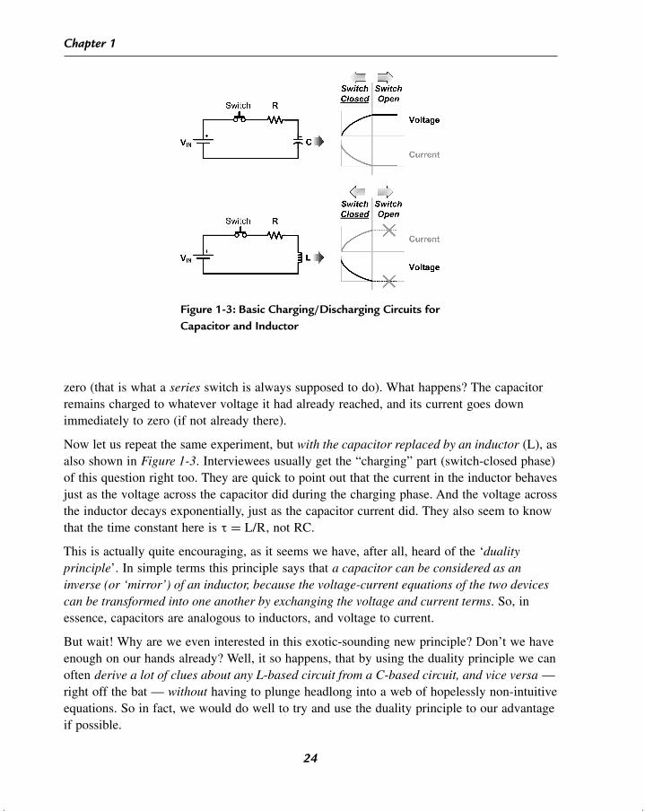
Let’s start by a simple question, one that is sometimes asked of a prospective power supplyhire (read “nervous interviewee”). This is shown in Figure 1-3.
Note that here we are using a mechanical switch for the sake of simplicity, thus alsoassuming it has none of the parasitics we talked about earlier. At time t = 0, we close theswitch (ON), and thus apply the dc voltage supply (VIN) across the capacitor (C) through thesmall series limiting resistor (R). What happens?
Most people get this right. The capacitor voltage increases according to the well-knownexponential curve VIN × (1 − e−t/τ), with a ‘time constant’ of τ = RC. The capacitor currenton the other hand, starts from a high initial value of VIN/R and then decays exponentiallyaccording to (VIN/R) × e−t/τ. Yes, if we wait “a very long time”, the capacitor would getcharged up almost fully to the applied voltage VIN, and the current would correspondinglyfall (almost) to zero. Let us now open the switch (OFF), though not necessarily havingwaited a very long time. In doing so we are essentially attempting to force the current to
23
Typeset by: CEPHA Imaging Pvt. Ltd., INDIA
[17:36 2006/4/19 Chap-01.tex] MANIKTALA: Switching Power Supplies A to Z Page: 24 1–60
Chapter 1
Figure 1-3: Basic Charging/Discharging Circuits forCapacitor and Inductor
zero (that is what a series switch is always supposed to do). What happens? The capacitorremains charged to whatever voltage it had already reached, and its current goes downimmediately to zero (if not already there).
Now let us repeat the same experiment, but with the capacitor replaced by an inductor (L), asalso shown in Figure 1-3. Interviewees usually get the “charging” part (switch-closed phase)of this question right too. They are quick to point out that the current in the inductor behavesjust as the voltage across the capacitor did during the charging phase. And the voltage acrossthe inductor decays exponentially, just as the capacitor current did. They also seem to knowthat the time constant here is τ = L/R, not RC.
This is actually quite encouraging, as it seems we have, after all, heard of the ‘dualityprinciple’. In simple terms this principle says that a capacitor can be considered as aninverse (or ‘mirror’) of an inductor, because the voltage-current equations of the two devicescan be transformed into one another by exchanging the voltage and current terms. So, inessence, capacitors are analogous to inductors, and voltage to current.
But wait! Why are we even interested in this exotic-sounding new principle? Don’t we haveenough on our hands already? Well, it so happens, that by using the duality principle we canoften derive a lot of clues about any L-based circuit from a C-based circuit, and vice versa —right off the bat — without having to plunge headlong into a web of hopelessly non-intuitiveequations. So in fact, we would do well to try and use the duality principle to our advantageif possible.
24

Typeset by: CEPHA Imaging Pvt. Ltd., INDIA
[17:36 2006/4/19 Chap-01.tex] MANIKTALA: Switching Power Supplies A to Z Page: 25 1–60
The Principles of Switching Power Conversion
With the duality principle in mind, let us attempt to open the switch in the inductor circuitand try to predict the outcome. What happens? No! Unfortunately, things don’t remainalmost “unchanged” as they did for a capacitor. In fact, the behavior of the inductor duringthe off-phase, is really no replica of the off-phase of the capacitor circuit.
So does that mean we need to jettison our precious duality principle altogether? Actually wedon’t. The problem here is that the two circuits in Figure 1-3, despite being deceptivelysimilar, are really not duals of each other. And for that reason, we really can’t use them toderive any clues either. A little later, we will construct proper dual circuits. But for now wemay have already started to suspect that we really don’t understand inductors as well as wethought, nor in fact the duality principle we were perhaps counting on to do so.
The Law of Conservation of Energy
If a nervous interviewee hazards the guess that the current in the inductor simply “goes tozero immediately” on opening the switch, a gentle reminder of what we all learnt in highschool is probably due. The stored energy in a capacitor is CV2/2, and so there is really noproblem opening the switch in the capacitor circuit — the capacitor just continues to hold itsstored energy (and voltage). But in an inductor, the stored energy is LI2/2. Therefore, if wespeculate that the current in the inductor circuit is at some finite value before the switch isopened and zero immediately afterwards, the question arises: where did all the storedinductor energy suddenly disappear? Hint: we have all heard of the law of conservation ofenergy — energy can change its form, but it just cannot be wished away!
Yes, sometimes a particularly intrepid interviewee will suggest that the inductor current“decays exponentially to zero” on opening the switch. So the question arises — where is thecurrent in the inductor flowing to and from? We always need a closed galvanic path forcurrent to flow (from Kirchhoff’s laws)!
But, wait! Do we even fully understand the charging phase of the inductor well enough?Now this is getting really troubling! Let’s find out for ourselves!
The Charging Phase and the Concept of Induced Voltage
From an intuitive viewpoint, most engineers are quite comfortable with the mental picturethey have acquired over time of a capacitor being charged — the accumulated charge keepstrying to repel any charge trying to climb aboard the capacitor plates, till finally a balance isreached and the incoming charge (current) gets reduced to near-zero. This picture is alsointuitively reassuring, because at the back of our minds, we realize it corresponds closelywith our understanding of real-life situations — like that of an over-crowded bus during rushhour, where the number of commuters that manage to get on board at a stop, depends on the
25
Typeset by: CEPHA Imaging Pvt. Ltd., INDIA
[17:36 2006/4/19 Chap-01.tex] MANIKTALA: Switching Power Supplies A to Z Page: 26 1–60
Chapter 1
capacity of the bus (double-decker or otherwise), and also on the sheer desperation of thecommuters (the applied voltage).
But coming to the inductor charging circuit (i.e. switch closed), we can’t seem to connectthis too readily to any of our immediate real-life experiences. Our basic question here is —why does the charging current in the inductor circuit actually increase with time. Orequivalently, what prevents the current from being high to start with? We know there is nomutually repelling “charge” here, as in the case of the capacitor. So why?
We can also ask an even more basic question — why is there any voltage even present acrossthe inductor? We always accept a voltage across a resistor without argument — because weknow Ohm’s law (V = I × R) all too well. But an inductor has (almost) no resistance — it isbasically just a length of solid conducting copper wire (wound on a certain core). So howdoes it manage to “hold-off” any voltage across it? In fact, we are comfortable about the factthat a capacitor can hold voltage across it. But for the inductor — we are not very clear!Further, if what we have learnt in school is true — that electric field by definition is thevoltage gradient dV/dx (“x” being the distance), we are now faced with having to explaina mysterious electric field somewhere inside the inductor! Where did that come from?
It turns out, that according to Lenz and/or Faraday, the current takes time to build up in aninductor only because of ‘induced voltage’. This voltage, by definition, opposes any externaleffort to change the existing flux (or current) in an inductor. So if the current is fixed, yes,there is no voltage present across the inductor — it then behaves just as a piece ofconducting wire. But the moment we try to change the current, we get an induced voltageacross it. By definition, the voltage measured across an inductor at any moment (whether theswitch is open or closed, as in Figure 1-3), is the ‘induced voltage’.
Note: We also observe that the analogy between a capacitor/inductor and voltage/current, as invoked by theduality principle, doesn’t stop right there! For example, it was considered equally puzzling at some point inhistory, how at all any current was apparently managing to flow through a capacitor — when the appliedvoltage across it was changed. Keeping in mind that a capacitor is basically two metal plates with aninterposing (non-conducting) insulator, it seemed contrary to the very understanding of what an “insulator”was supposed to be. This phenomenon was ultimately explained in terms of a ‘displacement current’, thatflows (or rather seems to flow) through the plates of the capacitor, when the voltage changes. In fact, thiscurrent is completely analogous to the concept of ‘induced voltage’ — introduced much later to explain thefact that a voltage was being observed across an inductor, when the current through it was changing.
So let us now try to figure out exactly how the induced voltage behaves when the switch isclosed. Looking at the inductor charging phase in Figure 1-3, the inductor current is initiallyzero. Thereafter, by closing the switch, we are attempting to cause a sudden change in thecurrent. The induced voltage now steps in to try to keep the current down to its initial value(zero). So we apply ‘Kirchhoff’s voltage law’ to the closed loop in question. Therefore,at the moment the switch closes, the induced voltage must be exactly equal to the appliedvoltage, since the voltage drop across the series resistance R is initially zero (by Ohm’s law).
26
Typeset by: CEPHA Imaging Pvt. Ltd., INDIA
[17:36 2006/4/19 Chap-01.tex] MANIKTALA: Switching Power Supplies A to Z Page: 27 1–60
The Principles of Switching Power Conversion
As time progresses, we can think intuitively in terms of the applied voltage “winning”. Thiscauses the current to rise up progressively. But that also causes the voltage drop across R toincrease, and so the induced voltage must fall by the same amount (to remain faithful toKirchhoff’s voltage law). That tells us exactly what the induced voltage (voltage acrossinductor) is during the entire switch-closed phase.
Why does the applied voltage “win”? For a moment, let’s suppose it didn’t. That would meanthe applied voltage and the induced voltage have managed to completely counter-balanceeach other — and the current would then remain at zero. However, that cannot be, becausezero rate of change in current implies no induced voltage either! In other words, the veryexistence of induced voltage depends on the fact that current changes, and it must change.
We also observe rather thankfully, that all the laws of nature bear each other out. There is nocontradiction whichever way we look at the situation. For example, even though the currentin the inductor is subsequently higher, its rate of change is less, and therefore, so is theinduced voltage (on the basis of Faraday’s/Lenz’s law). And this “allows” for the additionaldrop appearing across the resistor, as per Kirchhoff’s voltage law!
But we still don’t know how the induced voltage behaves when the switch turns OFF! Tounravel this part of the puzzle, we actually need some more analysis.
The Effect of the Series Resistance on the Time Constant
Let us ask — what are the final levels at the end of the charging phase in Figure 1-3 — i.e.of the current in the inductor, and the voltage across the capacitor. This requires us to focuson the exact role being played by R. Intuitively we expect that for the capacitor circuit,increasing the R will increase the charging time constant τ. This is borne out by the equationτ = RC too, and is what happens in reality too. But for the inductor charging circuit, we areagain up against another seemingly counter-intuitive behavior — increasing R actuallydecreases the charging time constant. That is in fact indicated by τ = L/R too.
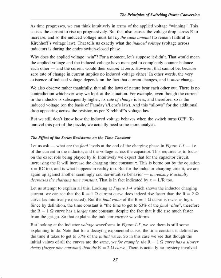
Let us attempt to explain all this. Looking at Figure 1-4 which shows the inductor chargingcurrent, we can see that the R = 1 Ω current curve does indeed rise faster than the R = 2 Ω
curve (as intuitively expected). But the final value of the R = 1 Ω curve is twice as high.Since by definition, the time constant is “the time to get to 63% of the final value”, thereforethe R = 1 Ω curve has a larger time constant, despite the fact that it did rise much fasterfrom the get-go. So that explains the inductor current waveforms.
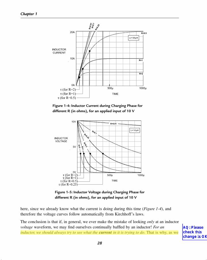
But looking at the inductor voltage waveforms in Figure 1-5, we see there is still someexplaining to do. Note that for a decaying exponential curve, the time constant is defined asthe time it takes to get to 37% of the initial value. So in this case we see that though theinitial values of all the curves are the same, yet for example, the R = 1 Ω curve has a slowerdecay (larger time constant) than the R = 2 Ω curve! There is actually no mystery involved
27
Typeset by: CEPHA Imaging Pvt. Ltd., INDIA
[17:36 2006/4/19 Chap-01.tex] MANIKTALA: Switching Power Supplies A to Z Page: 28 1–60
Chapter 1
Figure 1-4: Inductor Current during Charging Phase fordifferent R (in ohms), for an applied input of 10 V
Figure 1-5: Inductor Voltage during Charging Phase fordifferent R (in ohms), for an applied input of 10 V
here, since we already know what the current is doing during this time (Figure 1-4), andtherefore the voltage curves follow automatically from Kirchhoff’s laws.
The conclusion is that if, in general, we ever make the mistake of looking only at an inductorvoltage waveform, we may find ourselves continually baffled by an inductor! For aninductor, we should always try to see what the current in it is trying to do. That is why, as we
28
csekar
inductor, we should always try to see what the current in it is trying to do. That is why, as we
csekar
AQ: Please check this change is OK?
Typeset by: CEPHA Imaging Pvt. Ltd., INDIA
[17:36 2006/4/19 Chap-01.tex] MANIKTALA: Switching Power Supplies A to Z Page: 29 1–60
The Principles of Switching Power Conversion
just found out, the voltage during the off-time is determined entirely by the current. Thevoltage just follows the dictates of the current, not the other way around. In fact, inChapter 5, we will see how this particular behavioral aspect of an inductor determines theexact shape of the voltage and current waveforms during a switch transition, and therebydetermines the crossover (transition) loss too.
The Inductor Charging Circuit with R = 0, and the “Inductor Equation”
What happens if R is made to decrease to zero?
From Figure 1-5 we can correctly guess that the only reason that the voltage across theinductor during the on-time changes at all from its initial value VIN is the presence of R!So if R is 0, we can expect that the voltage across the inductor never changes during theon-time! The induced voltage must then be equal to the applied dc voltage. That is notstrange at all — if we look at it from the point of view of Kirchhoff’s voltage law, thereis no voltage drop present across the resistor — simply because there is no resistor! So inthis case, all the applied voltage appears across the inductor. And we know it can “hold-off”this applied voltage, provided the current in it is changing. Alternatively, if any voltage ispresent across an inductor, the current through it must be changing!
So now, as suggested by the low-R curves of Figure 1-4 and Figure 1-5, we expect that theinductor current will keep ramping up with a constant slope during the on-time. Eventually,it will reach an infinite value (in theory). In fact, this can be mathematically proven toourselves by differentiating the inductor charging current equation with respect to time, andthen putting R = 0 as follows
I(t) = VIN
R
(1 − e−tR/
L)
dI(t)
dt= VIN
R
(R
Le−tR/
L)
dI(t)
dt
∣∣∣∣R = 0
= VIN
L
So we see that when the inductor is connected directly across a voltage source VIN, the slopeof the line representing the inductor current is constant, and equal to VIN/L (the currentrising constantly).
Note that in the above derivation, the voltage across the inductor happened to be equal toVIN, because R was 0. But in general, if we call “V” the voltage actually present across theinductor (at any given moment), I being the current through it, we get the general
29
Typeset by: CEPHA Imaging Pvt. Ltd., INDIA
[17:36 2006/4/19 Chap-01.tex] MANIKTALA: Switching Power Supplies A to Z Page: 30 1–60
Chapter 1
“inductor equation”
dI
dt= V
L(inductor equation)
This equation applies to an ideal inductor (R = 0), in any circuit, under any condition.For example, it not only applies to the “charging” phase of the inductor, but also its“discharging” phase!
Note: When working with the inductor equation, for simplicity, we usually plug in only the magnitudes ofall the quantities involved (though we do mentally keep track of what is really happening — i.e. currentrising or falling).
The Duality Principle
We now know how the voltage and current (rather its rate of change), are mutually related inan inductor, during both the charging and discharging phases. Let us use this information,along with a more complete statement of the duality principle, to finally understand whatreally happens when we try to interrupt the current in an inductor.
“The principle of duality concerns the transformation between two apparently differentcircuits, which have similar properties when current and voltage are interchanged. Dualitytransformations are applicable to planar circuits only, and involve a topological conversion:capacitor and inductor interchange, resistance and conductance interchange, and voltagesource and current source interchange”.
We can thus spot our “mistakes” in Figure 1-3. First, we were using an input voltage sourceapplied to both circuits — whereas we should have used a current source for the “other”circuit. Second, we used a series switch in both the circuits. We note that the primaryfunction of a series switch is only to interrupt the flow of current — not to change thevoltage (though that may happen as a result). So if we really want to create proper mirror(dual) circuits, then forcing the current to zero in the inductor, is the dual of forcing thevoltage across the capacitor to zero. And to implement that, we obviously need to place aswitch in parallel to the capacitor (not in series with it). With these changes in mind,we have finally created true dual circuits as shown in Figure 1-6 (both are actually equallyimpractical in reality!).
The “Capacitor Equation”
To analyze what happens in Figure 1-6 we must first learn the “capacitor equation” —analogous to the “inductor equation” derived previously. If the duality principle is correct,
30
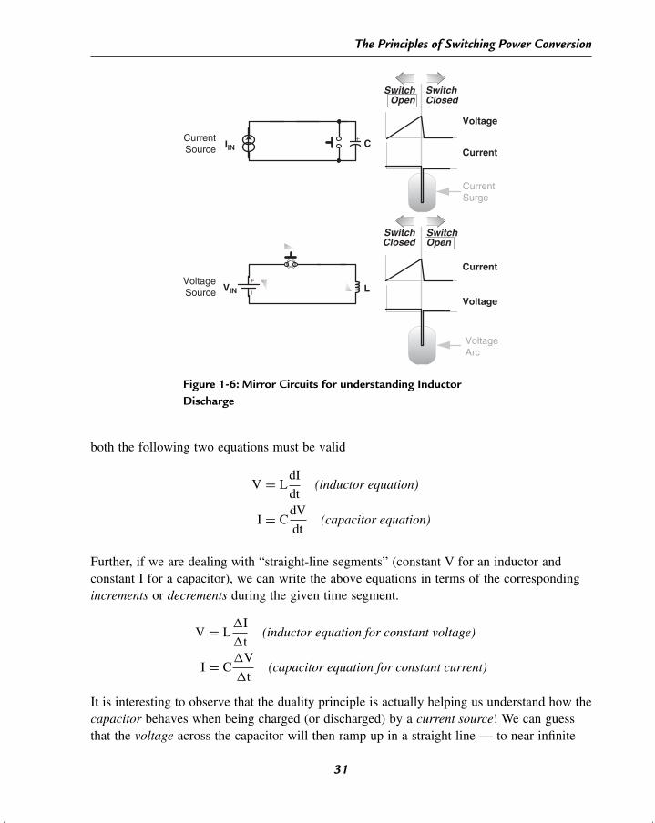
Typeset by: CEPHA Imaging Pvt. Ltd., INDIA
[17:36 2006/4/19 Chap-01.tex] MANIKTALA: Switching Power Supplies A to Z Page: 31 1–60
The Principles of Switching Power Conversion
CurrentSurge
+ CIIN
−+
LVIN
VoltageArc
CurrentSource
VoltageSource
SwitchClosed
SwitchOpen
SwitchClosed
SwitchOpen
Voltage
Current
Voltage
Current
Figure 1-6: Mirror Circuits for understanding InductorDischarge
both the following two equations must be valid
V = LdI
dt(inductor equation)
I = CdV
dt(capacitor equation)
Further, if we are dealing with “straight-line segments” (constant V for an inductor andconstant I for a capacitor), we can write the above equations in terms of the correspondingincrements or decrements during the given time segment.
V = L∆I
∆t(inductor equation for constant voltage)
I = C∆V
∆t(capacitor equation for constant current)
It is interesting to observe that the duality principle is actually helping us understand how thecapacitor behaves when being charged (or discharged) by a current source! We can guessthat the voltage across the capacitor will then ramp up in a straight line — to near infinite
31
Typeset by: CEPHA Imaging Pvt. Ltd., INDIA
[17:36 2006/4/19 Chap-01.tex] MANIKTALA: Switching Power Supplies A to Z Page: 32 1–60
Chapter 1
values — just as the inductor current does with an applied voltage source. And in both cases,the final values reached (of the voltage across the capacitor and the current through theinductor) are dictated only by various parasitics that we have not considered here — mainlythe ESR of the capacitor and the DCR of the inductor respectively.
The Inductor Discharge Phase
We now analyze the mirror circuits of Figure 1-6 in more detail.
We know intuitively (and also from the capacitor equation), what happens to a capacitorwhen we attempt to suddenly discharge it (by means of the parallel switch). Therefore, wecan now easily guess what happens when we suddenly try to “discharge” the inductor (i.e.force its current to zero by means of the series switch).
We know that if a “short” is applied across any capacitor terminals, we get an extremelyhigh current surge for a brief moment — during which time the capacitor discharges, and thevoltage across it ramps down steeply to zero. So we can correctly infer that if we try tointerrupt the current through an inductor, we will get a very high voltage across it — with thecurrent simultaneously ramping down steeply to zero. So the mystery of the inductor“discharge” phase is solved — with the help of the duality principle!
But we still don’t know exactly what the actual magnitude of the voltage spike appearingacross the switch/inductor is. That is simple — as we said previously, during the off-time,the voltage will take on any value to force current continuity. So a brief arc will appearacross the contacts as we try to pull them apart (see Figure 1-6). If the contacts are separatedby a greater distance, the voltage will increase automatically to maintain the spark. Andduring this time, the current will ramp down steeply. The arcing will last for as long as thereis any remaining inductor stored energy — i.e. till the current completely ramps down tozero. The rate of fall of current is simply V/L, from the inductor equation. So eventually, allthe stored energy in the inductor is completely dissipated in the resulting flash of heat andlight, and the current returns to zero simultaneously. At this moment, the induced voltagecollapses to zero too, its purpose complete. This is in fact the basic principle behind theautomotive spark plug, and the camera flash too (occurring in a more controlled fashion).
But wait — we have stated above that the rate of fall of current in the inductor circuit was“V/L”. What is V? V is the voltage across the inductor, not the voltage across the contacts.In the following sections, we will learn that the voltage across an inductor (almost always)reverses when we try to interrupt its current. If that is true, then by Kirchhoff’s voltage law,since the algebraic sum of all the voltage drops in any closed circuit must add up to zero, thevoltage across the contacts will be equal to the sum of the magnitudes of the induced voltageand the applied dc rail — however, the sign of the voltage across the contacts (i.e. itsdirection) will necessarily be opposite to the other voltages (see the gray triangles in the
32
Typeset by: CEPHA Imaging Pvt. Ltd., INDIA
[17:36 2006/4/19 Chap-01.tex] MANIKTALA: Switching Power Supplies A to Z Page: 33 1–60
The Principles of Switching Power Conversion
lower schematic of Figure 1-6 ). Therefore, we conclude that the magnitude of the voltagespike across the inductor is equal to the magnitude of the voltage across the contacts, minusthe magnitude of the input dc voltage.
Finally, we know everything about the puzzling inductor discharge phase!
Flyback Energy and Freewheeling Current
The energy that “must get out” of the inductor when we try to open the switch is called the‘flyback’ energy. The current that continues to force its way through, is called the‘freewheeling’ current. Note that this not only sounds, but in fact is, very similar to anotherreal-world situation — that of a mechanical spinning wheel, or a ‘flywheel’. In fact,understanding the flywheel can help greatly in gaining an intuitive insight into the behaviorof an inductor.
Just as the inductor has stored energy related to the current flowing through it, the flywheelstores energy related to its spinning action. And neither of these energy terms can be wishedaway in an instant. In the case of the flywheel, we can apply “brakes” to dissipate itsrotational energy (as heat in the brake linings) — and we know this will produce aprogressive reduction in the spinning. Further, if the brakes are applied more emphatically,the time that will elapse till the spinning stops entirely, gets proportionately decreased. Thatis very similar to an inductor — with the induced voltage (during the off-time) playing the partof the “brakes”, and the current being akin to the spinning. So, the induced voltage causes aprogressive reduction in the current. If we have a higher induced voltage, this will cause asteeper fall in the current. In fact, that is also indicated by the inductor equation V = LdI/dt!
However, we have also learned something more fundamental about the behavior of aninductor, as described next.
Current Must Be Continuous, Its Slope Need Not Be
The key word in the previous section was progressive. From a completelymathematical/geometrical point of view now, we should understand that any curverepresenting inductor current cannot be discontinuous (no sudden jumps allowed) — becausethat will in effect cause energy to be discontinuous, which we know is impossible. But wecan certainly cause the slope of the current (i.e. its dI/dt) to have “jumps”. So we can forexample, change the slope of current (dI/dt) in an instant — from one representing a risingramp (increasing stored energy), to one representing a falling ramp (opposite sign, i.e.decreasing energy). However, the current itself must always be continuous. This is shown inFigure 1-7, under the choices marked “possible”.
Note that there are two options in the figure that are “possible”. Both are so, simply becausethey do not violate any known physical laws. However, one of these choices is considered
33
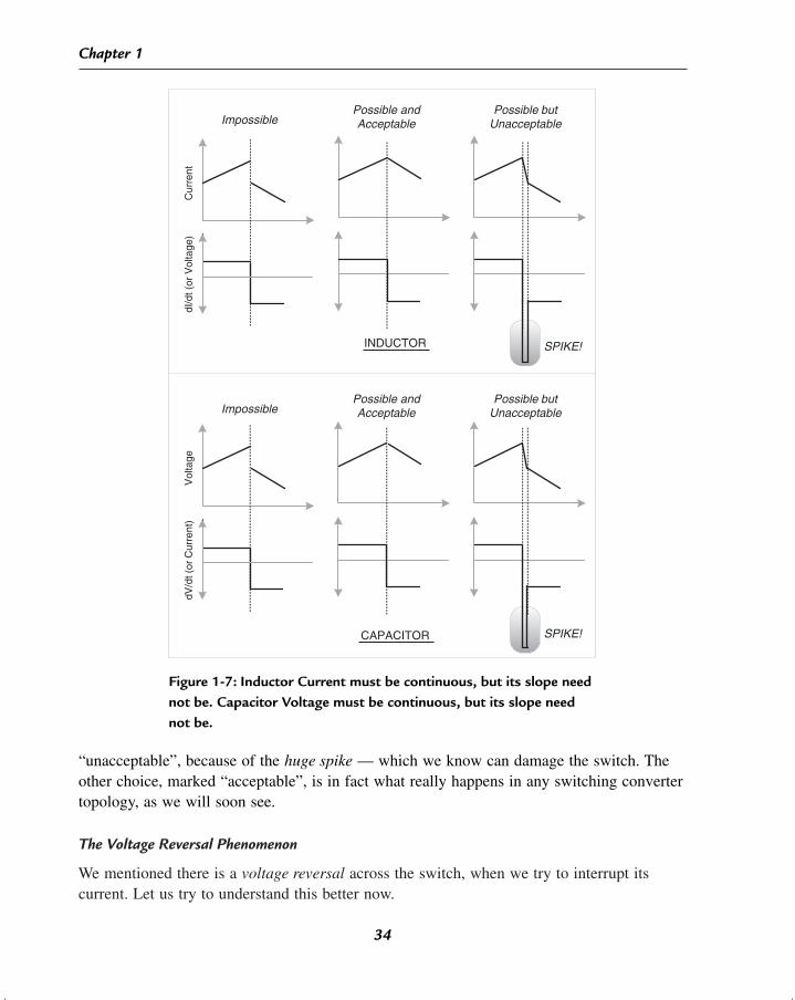
Typeset by: CEPHA Imaging Pvt. Ltd., INDIA
[17:36 2006/4/19 Chap-01.tex] MANIKTALA: Switching Power Supplies A to Z Page: 34 1–60
Chapter 1
SPIKE!
SPIKE!
Cur
rent
Vol
tage
dI/d
t (or
Vol
tage
)dV
/dt (
or C
urre
nt)
Possible andAcceptable
Possible butUnacceptableImpossible
Possible andAcceptable
Possible butUnacceptableImpossible
INDUCTOR
CAPACITOR
Figure 1-7: Inductor Current must be continuous, but its slope neednot be. Capacitor Voltage must be continuous, but its slope neednot be.
“unacceptable”, because of the huge spike — which we know can damage the switch. Theother choice, marked “acceptable”, is in fact what really happens in any switching convertertopology, as we will soon see.
The Voltage Reversal Phenomenon
We mentioned there is a voltage reversal across the switch, when we try to interrupt itscurrent. Let us try to understand this better now.
34
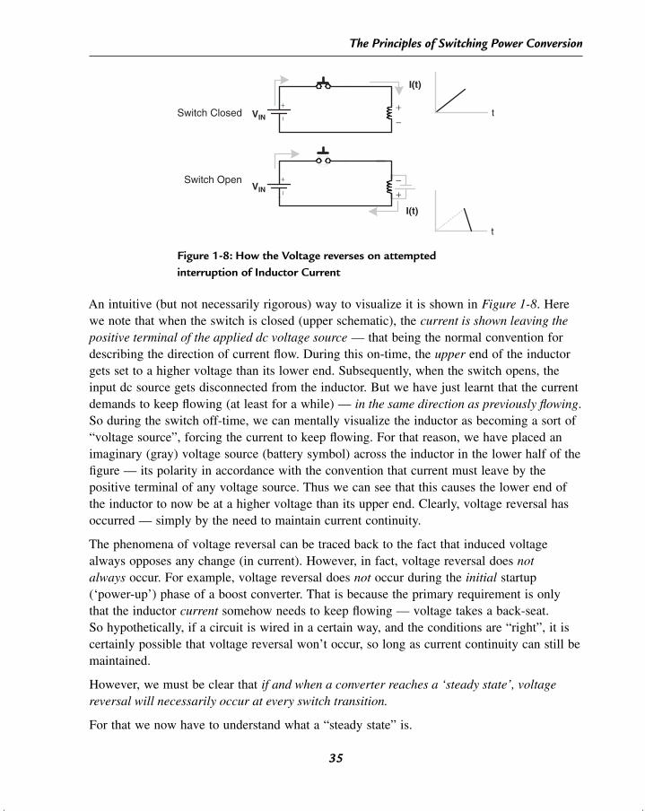
Typeset by: CEPHA Imaging Pvt. Ltd., INDIA
[17:36 2006/4/19 Chap-01.tex] MANIKTALA: Switching Power Supplies A to Z Page: 35 1–60
The Principles of Switching Power Conversion
−+
VIN
I(t)
I(t)
VIN −+
+−
+−
t
t
Switch Closed
Switch Open
Figure 1-8: How the Voltage reverses on attemptedinterruption of Inductor Current
An intuitive (but not necessarily rigorous) way to visualize it is shown in Figure 1-8. Herewe note that when the switch is closed (upper schematic), the current is shown leaving thepositive terminal of the applied dc voltage source — that being the normal convention fordescribing the direction of current flow. During this on-time, the upper end of the inductorgets set to a higher voltage than its lower end. Subsequently, when the switch opens, theinput dc source gets disconnected from the inductor. But we have just learnt that the currentdemands to keep flowing (at least for a while) — in the same direction as previously flowing.So during the switch off-time, we can mentally visualize the inductor as becoming a sort of“voltage source”, forcing the current to keep flowing. For that reason, we have placed animaginary (gray) voltage source (battery symbol) across the inductor in the lower half of thefigure — its polarity in accordance with the convention that current must leave by thepositive terminal of any voltage source. Thus we can see that this causes the lower end ofthe inductor to now be at a higher voltage than its upper end. Clearly, voltage reversal hasoccurred — simply by the need to maintain current continuity.
The phenomena of voltage reversal can be traced back to the fact that induced voltagealways opposes any change (in current). However, in fact, voltage reversal does notalways occur. For example, voltage reversal does not occur during the initial startup(‘power-up’) phase of a boost converter. That is because the primary requirement is onlythat the inductor current somehow needs to keep flowing — voltage takes a back-seat.So hypothetically, if a circuit is wired in a certain way, and the conditions are “right”, it iscertainly possible that voltage reversal won’t occur, so long as current continuity can still bemaintained.
However, we must be clear that if and when a converter reaches a ‘steady state’, voltagereversal will necessarily occur at every switch transition.
For that we now have to understand what a “steady state” is.
35
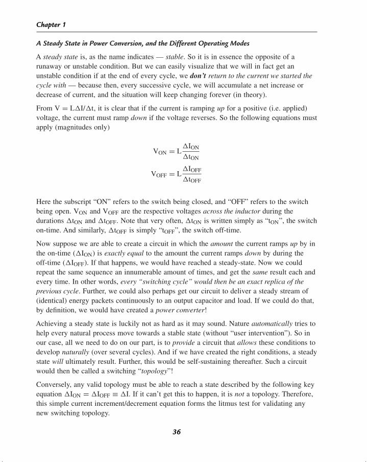
Typeset by: CEPHA Imaging Pvt. Ltd., INDIA
[17:36 2006/4/19 Chap-01.tex] MANIKTALA: Switching Power Supplies A to Z Page: 36 1–60
Chapter 1
A Steady State in Power Conversion, and the Different Operating Modes
A steady state is, as the name indicates — stable. So it is in essence the opposite of arunaway or unstable condition. But we can easily visualize that we will in fact get anunstable condition if at the end of every cycle, we don’t return to the current we started thecycle with — because then, every successive cycle, we will accumulate a net increase ordecrease of current, and the situation will keep changing forever (in theory).
From V = L∆I/∆t, it is clear that if the current is ramping up for a positive (i.e. applied)voltage, the current must ramp down if the voltage reverses. So the following equations mustapply (magnitudes only)
VON = L∆ION
∆tON
VOFF = L∆IOFF
∆tOFF
Here the subscript “ON” refers to the switch being closed, and “OFF” refers to the switchbeing open. VON and VOFF are the respective voltages across the inductor during thedurations ∆tON and ∆tOFF. Note that very often, ∆tON is written simply as “tON”, the switchon-time. And similarly, ∆tOFF is simply “tOFF”, the switch off-time.
Now suppose we are able to create a circuit in which the amount the current ramps up by inthe on-time (∆ION) is exactly equal to the amount the current ramps down by during theoff-time (∆IOFF). If that happens, we would have reached a steady-state. Now we couldrepeat the same sequence an innumerable amount of times, and get the same result each andevery time. In other words, every “switching cycle” would then be an exact replica of theprevious cycle. Further, we could also perhaps get our circuit to deliver a steady stream of(identical) energy packets continuously to an output capacitor and load. If we could do that,by definition, we would have created a power converter!
Achieving a steady state is luckily not as hard as it may sound. Nature automatically tries tohelp every natural process move towards a stable state (without “user intervention”). So inour case, all we need to do on our part, is to provide a circuit that allows these conditions todevelop naturally (over several cycles). And if we have created the right conditions, a steadystate will ultimately result. Further, this would be self-sustaining thereafter. Such a circuitwould then be called a switching “topology”!
Conversely, any valid topology must be able to reach a state described by the following keyequation ∆ION = ∆IOFF ≡ ∆I. If it can’t get this to happen, it is not a topology. Therefore,this simple current increment/decrement equation forms the litmus test for validating anynew switching topology.
36
Typeset by: CEPHA Imaging Pvt. Ltd., INDIA
[17:36 2006/4/19 Chap-01.tex] MANIKTALA: Switching Power Supplies A to Z Page: 37 1–60
The Principles of Switching Power Conversion
Note that the inductor equation, and thereby the definition of ‘steady state’, refers only to theincrease/decrease in current — it says nothing about the actual (absolute) value of thecurrent at the start (and end) of every cycle. So there are in fact several possibilities. Wecould have a steady state in which the current returns to zero every cycle, and this is calleda ‘discontinuous conduction mode’ (DCM). However, if the current stays pegged at somenon-zero value throughout, we will have ‘continuous conduction mode’ (CCM). The lattermode is the most common mode of operation encountered in power conversion. InFigure 1-9 we have graphically shown these operating modes (all in steady state). We alsohave some other modes that we will talk about very soon. Note that in the figure, the“square” waveform is the voltage across the inductor, and the slowly ramping waveform isthe inductor current. Let us make some related observations:
a) We see that the voltage across the inductor always reverses at every switching event(as expected in steady state).
b) We note that since the inductor equation relates voltage to the slope of the current,not to the actual current, therefore, for a given VON and VOFF, several currentwaveforms are possible (all having the same dI/dt for corresponding segments).Each of these possibilities has a name — CCM, DCM, BCM (boundary conductionmode, also called critical conduction mode), and so on. Which of these operatingmodes actually occurs, depends on the specific circuit (i.e. the topology), and alsothe application conditions (how much output power we are demanding, and what theinput and output voltages are).
c) The inductor voltages, VON and VOFF shown in the figure, are related to theapplication conditions VIN and/or VO. Their exact relationship will become known alittle later, and we will also learn that it depends on the specific topology.
d) A key question is — what is the exact relationship between the average inductorcurrent and the load current? We will soon see that that too depends on the specifictopology. However, in all cases, the average inductor current (“IAVG” or “IL”) isproportional to the load current (“IO”). So if for example IO is 2 A and IAVG is 10 A,then if IO is decreased to 1 A, IAVG will fall to 5 A. Therefore on decreasing theload current, we can get IAVG to decrease, as indicated in Figure 1-9.
e) Typically, we transit automatically from CCM to DCM, just by reducing the loadcurrent of the converter. But note that we will necessarily have to pass throughBCM along the way.
f) “BCM” is just that — a ‘boundary conduction mode’ — situated exactly betweenCCM and DCM. It is therefore a purely philosophical question to ask whether BCMshould be viewed as CCM or DCM (at their respective extremes) — it really doesn’tmatter.
37
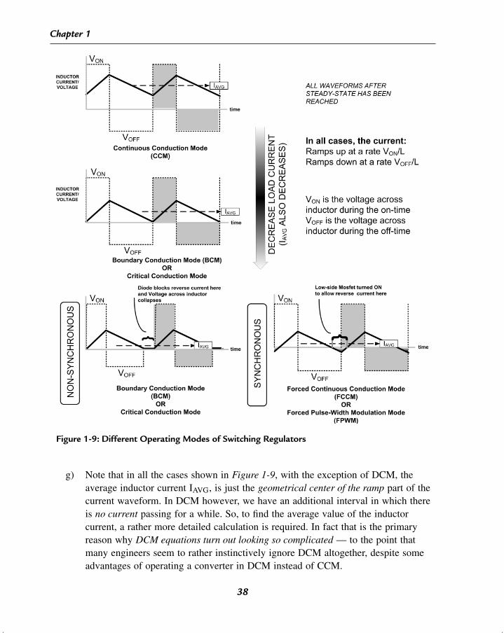
Typeset by: CEPHA Imaging Pvt. Ltd., INDIA
[17:36 2006/4/19 Chap-01.tex] MANIKTALA: Switching Power Supplies A to Z Page: 38 1–60
Chapter 1
Figure 1-9: Different Operating Modes of Switching Regulators
g) Note that in all the cases shown in Figure 1-9, with the exception of DCM, theaverage inductor current IAVG, is just the geometrical center of the ramp part of thecurrent waveform. In DCM however, we have an additional interval in which thereis no current passing for a while. So, to find the average value of the inductorcurrent, a rather more detailed calculation is required. In fact that is the primaryreason why DCM equations turn out looking so complicated — to the point thatmany engineers seem to rather instinctively ignore DCM altogether, despite someadvantages of operating a converter in DCM instead of CCM.
38
Typeset by: CEPHA Imaging Pvt. Ltd., INDIA
[17:36 2006/4/19 Chap-01.tex] MANIKTALA: Switching Power Supplies A to Z Page: 39 1–60
The Principles of Switching Power Conversion
Note: Expectedly, all DCM equations lead to exactly the same numerical results as the CCMequations — when the converter is in BCM. Practically speaking, we can freely pick and choosewhether to use the CCM equations, or the more formidable looking DCM equations, forevaluating a converter in BCM. Of course, there is no reason why we would ever want to strugglethrough complicated equations, when we can use much simpler equations to get the same results!
h) What really is the average inductor current “IAVG” as shown in Figure 1-9? A niceway to understand this parameter is through the “car analogy”. Suppose we pressthe gas pedal of a car. The car responds by increasing its speed. In an analogousfashion, when we apply a voltage across an inductor (the on-time voltage “VON”),the current ramps up. Subsequently, suppose we press on the brakes of the car. Thecar will then respond by decreasing its speed. Similarly, when the applied voltage isremoved from the inductor, voltage reversal occurs, and an induced voltage (the“brakes”) appears across the inductor, “VOFF”. Since it is in the opposite directionas VON, it causes the current to ramp down. So now, if we press the gas pedal(VON), followed by the brakes (VOFF), in quick succession, and with the righttiming, we could still make the car continue to move forward despite the constantlurching. It would then have a certain average speed — depending on the ratio ofthe gas pedal duration and the subsequent braking duration. In power conversion,this “lurching” is analogous to the ‘current ripple’ ∆I = ∆ION = ∆IOFF. And quitesimilarly, we have an ‘average inductor current’ IAVG too, as shown in Figure 1-9.However, we do understand that in a power converter, the output capacitoreventually absorbs (or smoothens) this “lurching”, and thus manages to deliver asteady dc current to the load as desired.
i) Some control ICs manage to maintain the converter in BCM mode under allapplication conditions. Examples of these are certain types of ‘hystereticcontrollers’, and self-oscillating types called ‘ringing choke converters’ (RCCs).However, we know that the current ramps down at a rate V/L. And since V dependson the input/output voltages, the time to get to zero current depends on the specificapplication conditions. Therefore, in any BCM implementation, we always lose theadvantage of fixed switching frequency operation.
j) Most conventional topologies are nowadays labeled ‘non-synchronous’ — todistinguish them from more recent ‘synchronous’ topologies. In the former, a diodeis always present (the catch diode), that prevents the inductor current from reversingdirection, any time during the switching cycle. That is why, on reducing outputpower and/or increasing input voltage, we automatically transit from CCM to DCM.However, in synchronous topologies, the catch diode is either supplanted orcompletely replaced by a ‘low-drop’ mosfet across it. So whenever the diode issupposed to conduct, we force this extra mosfet into conduction for that duration.Since the drop across this mosfet is much lower than across a diode, not only do we
39
Typeset by: CEPHA Imaging Pvt. Ltd., INDIA
[17:36 2006/4/19 Chap-01.tex] MANIKTALA: Switching Power Supplies A to Z Page: 40 1–60
Chapter 1
manage to significantly reduce the conduction loss in the freewheeling path, but wecan also now allow reverse inductor current — i.e. current moving instantaneouslyaway from the load. However note that the average inductor current could still bepositive — see Figure 1-9. Further, with negative currents now being “allowed”,we no longer get DCM on reducing output power, but rather enter FPWM/FCCMas described in the figure.
Note: It is fortunate that almost all the standard CCM design equations (for non-synchronoustopologies) apply equally to FCCM. So from the viewpoint of a harried designer, one of the“advantages” of using synchronous topologies is that the complicated DCM equations are a thingof the past! Though there are some new complications and nuances of synchronous topologies thatwe need to understand eventually.
The Voltseconds Law, Inductor Rest and Converter Duty Cycle
There is another way to describe a steady state, by bringing in the inductor equationV = L∆I/∆t.
We know that during a steady state ∆ION = ∆IOFF ≡ ∆I. So what we are also saying is that
“In steady state, the product of the voltage applied across the inductor, multiplied by theduration we apply it for (i.e. the on-time), must be equal to the voltage that appears across theinductor during the off-time, multiplied by the duration that lasts for”.
Therefore we get
VON × t ON = VOFF × t OFF
The product of the voltage, and the time for which it appears across the inductor, is calledthe ‘voltseconds’ across the inductor. So equivalently, what we are also saying is that
“If we have an inductor in a steady state, the voltseconds present across it during the on-time(i.e. current ramp-up phase), must be exactly equal in magnitude, though opposite in sign, tothe voltseconds present across it during the off-time (i.e. during the current ramp-down phase)”.
That also means that if we plot the inductor voltage versus time, the area under the voltagecurve during the on-time must be equal to the area under the voltage curve during the off-time.But we also know that voltage reversal always occurs in steady state. So clearly, these twoareas must have the opposite sign. See the vertically and horizontally hatched segments inFigure 1-9.
Therefore, we can also say that the net area under the voltage curve of an inductor must beequal to zero (in any switching cycle under steady state operation).
Note that since the typical times involved in modern switching power conversion are sosmall, “voltseconds” turns out to be a very small number. Therefore, to make numbers more
40
Typeset by: CEPHA Imaging Pvt. Ltd., INDIA
[17:36 2006/4/19 Chap-01.tex] MANIKTALA: Switching Power Supplies A to Z Page: 41 1–60
The Principles of Switching Power Conversion
manageable, we usually prefer to talk in terms of ‘Et’ or the ‘voltµseconds’. Et is clearly justthe voltage applied across the inductor multiplied by the time in microseconds (not seconds).Further, we know that typical inductance values used in power conversion are also betterexpressed in terms of “µH” (microhenries), not H. So from V = LdI/dt we can write
∆ION = VON × tON
L= VON × tON_µH
LµH= Et
LµH
or simply
∆I = Et
L(steady state, L in µH)
Note: If in any given equation, Et and L appear together, it should be generally assumed that L is in µH.Similarly, if we are using voltseconds, that would usually imply L is in H (unless otherwise indicated).
Another term often used in power, one that tells us that we have managed to return to thesame inductor current (and energy) that we started off with, is called inductor ‘reset’. Resetoccurs at the very moment when the equality ∆IOFF = ∆ION is established. Of course, wecould also have a non-repetitive (or ‘single-shot’) event, where the current starts at zero andthen returns to zero — and that too would be inductor “reset”.
The corollary is that in a repetitive switching scenario (steady state), an inductor must beable to reset every cycle. Reversing the argument — any circuit configuration that makesinductor reset an impossibility, is not a viable switching topology.
When we switch repetitively at a switching frequency “f”, the ‘time period’ (T) is equalto 1/f. We can also define the ‘duty cycle’ (D) of a power converter as the ratio of theon-time of the switch, to the time period. So
D = tON
T(duty cycle definition)
Note that we can also write this as
D = tON
tON + (T − tON)(duty cycle definition)
At this point we should be very clear how we are defining “tOFF” in particular. Whileapplying the voltseconds law, we had implicitly assumed that tOFF was the time for which theinduced voltage VOFF lasts, not necessarily the time for which the switch is OFF(i.e. T − tON). In DCM they are not the same (see Figure 1-9)! Only in CCM do we get
tOFF = T − tON (duty cycle in CCM)
41
Typeset by: CEPHA Imaging Pvt. Ltd., INDIA
[17:36 2006/4/19 Chap-01.tex] MANIKTALA: Switching Power Supplies A to Z Page: 42 1–60
Chapter 1
and therefore
D = tON
tON + tOFF(duty cycle in CCM)
If working in DCM, we should stick to the more general definition of duty cycle giveninitially.
Using and Protecting Semiconductor Switches
We realize that all topologies exist only because they can achieve a steady state. In an“experimental” topology in which we can’t make ∆ION = ∆IOFF happen, the inductor maysee a net increase of current every cycle, and this can eventually escalate to a very large,almost uncontrolled value of current in just a few cycles. The name given to this progressiveramping-up (or down) of current (or inductor energy), one that is ultimately limited only byparasitics like the ESR and DCR, is called ‘staircasing’. The switch will also turn ON intothe same current, and can thus be destroyed — that is if the induced voltage spike hasn’talready done so (which can happen, if the situation is anything similar to the “unacceptable”plots shown in Figure 1-7!).
Note: The very use of the inductor equation V = LdI/dt actually implies we are ignoring its parasiticresistance, DCR. The inductor equation is an idealization, applying only to a “perfect” inductor. That is whywe had to put R = 0 when we derived it previously.
In an actual power supply, the “mechanical switch” is replaced with a modern semiconductordevice (like the mosfet) — largely because then the switching action can be implementedreliably, and also at a very high repetition rate. But semiconductor devices have certainelectrical ratings that we need to be well aware of.
Every semiconductor device has an ‘absolute maximum voltage rating’ that, unlike anytypical mechanical relay, cannot be exceeded even momentarily — without possibly causingits immediate destruction. So most mosfets do not allow any “latitude” whatsoever, in termsof their voltage ratings.
Note: There are some ‘avalanche-rated’ mosfets available, which can internally ‘clamp’ the excess voltageappearing across them to some extent. In doing so, they are basically dissipating the excess energyassociated with the voltage spike, within their internal clamp. Therefore, they can survive a certain amountof excess voltage (and energy), but only for a short duration (since the device heats up quickly).
There is also a maximum semiconductor device ‘current rating’, but that is usually morelong-term in nature, dictated by the comparatively slower process of internal heat build-upinside the device. So hypothetically speaking, we could perhaps exceed the current ratingsomewhat, though only for a short time. Of course we don’t want to run a device constantlyin this excess-current condition. However, under ‘abnormal conditions’, like an “overload”on the output of the converter (or the extreme case of a shorted output), we may judiciously
42
Typeset by: CEPHA Imaging Pvt. Ltd., INDIA
[17:36 2006/4/19 Chap-01.tex] MANIKTALA: Switching Power Supplies A to Z Page: 43 1–60
The Principles of Switching Power Conversion
allow for a certain amount of “abuse” with regards to the current rating — but certainly notwith the voltage rating!
In a practical implementation, we have to design the converter, select the switch, and thenlay it all out on a printed circuit board (PCB) with great care — to ensure in particular thatthere is no voltage spike that can “kill” the switch (nor any other semiconductor devicespresent on the board). Occasionally, we may therefore need to add an external ‘snubber’ or‘clamp’ across the switch, so as to truncate any remnant spikes to within the voltage ratingsof the switch.
To protect the switch (and converter) from excess currents, a ‘current limit’ is usuallyrequired. In this case, the current in the inductor, or in the switch, is sensed, and thencompared against a set threshold. If and when that is momentarily exceeded, the controlcircuitry forces the switch to turn OFF immediately for the remainder of the switching cycle,so as to protect itself. In the next cycle, no “memory” is usually retained of what may havehappened in the preceding cycle. Therefore, every switching cycle is started “afresh”, withthe current being continuously monitored to ensure it is at a “safe” level. If not, protectiveaction is again initiated, and can go be repeated every cycle for several cycles if necessary,until the “overcurrent” condition ceases.
Note: One of the best-known examples of the perils of “previous-cycle memory” in implementingcurrent limit occurs in the popular “Simple Switcher®” family of parts (at www.national.com). In the“third generation” LM267x family, the control circuit rather surprisingly reduces the duty cycle to about45% for several cycles after any single current limit event. It then tries to progressively allow the dutycycle to increase over several successive cycles back to its required value. But this causes severe output‘foldback’ and consequent inability to regulate up to full rated load, particularly in applications that requirea duty cycle greater than 50%. This condition is further exacerbated with large output capacitances, becausethe higher currents required to charge the output capacitor after the removal of an abnormal condition(e.g. output short), can lead to another current limit event (and consequent foldback for several cyclesagain) — before the duty cycle has been able to return to its desired value. In effect the converter goesinto a continuous “motorboating” condition on removal of the output short, and so the output neverrecovers. This is rather obliquely “revealed” only deep within the product datasheets (liability cover?).
With the introduction to power conversion now complete, we turn our attention to howswitching topologies develop naturally out of the behavior of an inductor.
Evolution of Switching TopologiesControlling the Induced Voltage Spike by Diversion through a Diode
We realize that our “problem” with using an inductor is two-fold: either we are going to landup with a near-infinite induced voltage spikes, as shown in Figure 1-6 and Figure 1-7. Or ifwe do somehow manage to control the induced voltage to some finite level, the equationV = LdI/dt tells us we could very well end up with near-infinite currents (staircasing).
43
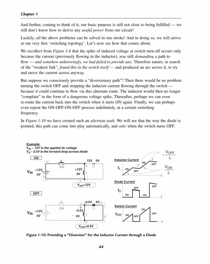
Typeset by: CEPHA Imaging Pvt. Ltd., INDIA
[17:36 2006/4/19 Chap-01.tex] MANIKTALA: Switching Power Supplies A to Z Page: 44 1–60
Chapter 1
And further, coming to think of it, our basic purpose is still not close to being fulfilled — westill don’t know how to derive any useful power from our circuit!
Luckily, all the above problems can be solved in one stroke! And in doing so, we will arriveat our very first ‘switching topology’. Let’s now see how that comes about.
We recollect from Figure 1-6 that the spike of induced voltage at switch turn-off occurs onlybecause the current (previously flowing in the inductor), was still demanding a path toflow — and somehow unknowingly, we had failed to provide any. Therefore nature, in searchof the “weakest link”, found this in the switch itself — and produced an arc across it, to tryand move the current across anyway.
But suppose we consciously provide a “diversionary path”? Then there would be no problemturning the switch OFF and stopping the inductor current flowing through the switch —because it could continue to flow via this alternate route. The inductor would then no longer“complain” in the form of a dangerous voltage spike. Thereafter, perhaps we can evenre-route the current back into the switch when it turns ON again. Finally, we can perhapseven repeat the ON-OFF-ON-OFF process indefinitely, at a certain switchingfrequency.
In Figure 1-10 we have created such an alternate path. We will see that the way the diode ispointed, this path can come into play automatically, and only when the switch turns OFF.
−+
−+
ON
OFF
0V
+12V
0V
+12V
0V
+12V
0V
−0.5V
Example:VIN = 12V is the applied dc voltageVD = 0.5V is the forward drop across diode
0V12V
0V−0.5V
L
VIN
IL
ID
ISWVIN
SW D
L
SW D
t
ON
tON
t
OFF
OFF
OFFOFF
OFFOFF
ON
ON
ON
ON
Diode Current
Switch Current
Inductor Current
VON=12V
VOFF=0.5V
L
VON
L
VOFF−
Figure 1-10: Providing a “Diversion” for the Inductor Current through a Diode
44
Typeset by: CEPHA Imaging Pvt. Ltd., INDIA
[17:36 2006/4/19 Chap-01.tex] MANIKTALA: Switching Power Supplies A to Z Page: 45 1–60
The Principles of Switching Power Conversion
Just to make things clearer, we have used some sample numbers in Figure 1-10. We havetaken the applied input voltage to be 12 V, and assumed a typical Schottky diode forwarddrop of 0.5 V. Note that we are assuming a “perfect” switch here (no forward drop), for thesake of simplicity. We make the following observations:
When the switch is ON (closed), the voltage at the upper end of the inductor L is at12 V and the lower end is at 0 V (‘ground’). So the diode is reverse-biased and doesnot conduct. Energy is then being built up in the inductor by the applied dc voltagesource.
The magnitude of the voltage applied across the inductor during the on-time of theswitch (i.e. ‘VON ’), is equal to 12 V.
When the switch turns OFF (open), an alternate path is available for the inductorcurrent to flow — through the diode. And we can be sure that “nature” (in our casethe “induced voltage”) will attempt to exploit this path — by forcing the diode toconduct. But for that, the diode must get ‘forward-biased’ i.e. its anode must get to avoltage 0.5 V higher than the cathode. But the anode is being held at ground (0 Vrail). Therefore, the cathode must fall to −0.5 V.
The magnitude of the voltage applied across the inductor during the off-time of theswitch (i.e. ‘VOFF’), is equal to 0.5 V.
Note that the induced voltage during the switch off-time, has had its polarityreversed.
The rate of rise of the current (in the inductor and switch) during the on-time is equalto VON/L. And during the off-time, the current ramps down (much more slowly), at arate of VOFF/L (in the inductor and diode).
Yes, if we wait long enough the inductor current will finally ramp down to zero(inductor ‘reset’). But if we don’t wait, and turn the switch back ON again, thecurrent will again start to ramp up (staircasing), as shown in Figure 1-10.
Note that both the switch and diode currents have a “choppy” waveform — sinceone takes over where the other left off. This is in fact always true for any switchingpower converter (or topology).
Summarizing: We see that having provided a diversionary path for the current, the inductorisn’t ‘complaining’ anymore, and there is no uncontrolled induced voltage spike anymore.But we certainly have now landed up with a possible problem of escalating currents. Andcoming to think of it, neither do we have a useful output rail yet, which is what we arebasically looking to do finally. In fact, all that we are accomplishing in Figure 1-10 isdissipating some of the stored energy built up in the inductor during the on-time, within thediode during the off-time.
45
Typeset by: CEPHA Imaging Pvt. Ltd., INDIA
[17:36 2006/4/19 Chap-01.tex] MANIKTALA: Switching Power Supplies A to Z Page: 46 1–60
Chapter 1
Achieving a Steady State and Deriving useful Energy
We realize, that to prevent staircasing, we need to somehow induce voltseconds balance. Yes,as mentioned, we could perhaps wait long enough before turning the switch ON again. Butthat still won’t give us a useful output rail.
To finally solve all our problems in one go, let us take a hint from our “natural world ofvoltages”. Since we realize we are looking for an output dc voltage rail, isn’t it natural to usea capacitor somewhere in the circuit of Figure 1-10? Let us therefore now interpose acapacitor in series with the diode, as shown in Figure 1-11. If we do that, the diode(freewheeling) current would charge the capacitor up — and hopefully the capacitor voltagewould eventually reach a steady level ‘VO’! Further, since that would increase the voltagedrop appearing across the inductor during the off-time (VOFF), it would increase the rate atwhich the inductor current can ramp down — which we recognize was the basic problemwith the circuit in Figure 1-10. So we are finally seeing light at the end of the tunnel — bymaking VOFF comparable to VON, we are hoping to achieve voltseconds balance expressedby VON × tON = VOFF × tOFF.
In Figure 1-11 the current escalates initially, but then after several cycles, automaticallylevels out, in what is clearly a steady state. That is because every cycle the capacitor chargesup, it progressively increases the slope of the down-ramp, eventually allowing the converterto settle down naturally in to the basic condition ∆ION = ∆IOFF ≡ ∆I. And once that isachieved, it is self-sustaining!
We also have a useful rail now — available across the output capacitor, from which we candraw some stored energy. So we have shown a dc current passing through to the load by thedashed arrows in Figure 1-11.
In fact, this is our very first switching topology — the buck-boost topology.
Note: Under the abnormal condition of an output short for example, Figure 1-11 effectively reduces toFigure 1-10! Therefore, to protect the converter under such conditions, a current limit is required.
The Buck-Boost Converter
To understand Figure 1-11 better, we are actually going to work backwards from here. So letus assume we have achieved a steady state — and therefore the output capacitor too hasreached a steady value of say, 5 V. Let us now find the conditions needed to make that areality.
In Figure 1-11 the slope of the rising ramp is unchanged every cycle, being equal to VIN/L.The slope of the falling ramp is initially VD/L, where “VD” is the drop across the diode. Sofrom the inductor equation, initially ∆ION > ∆IOFF. Thus the current starts to staircase. Butthe magnitude of the slope of the falling ramp, and therefore ∆IOFF, keeps getting larger and
46
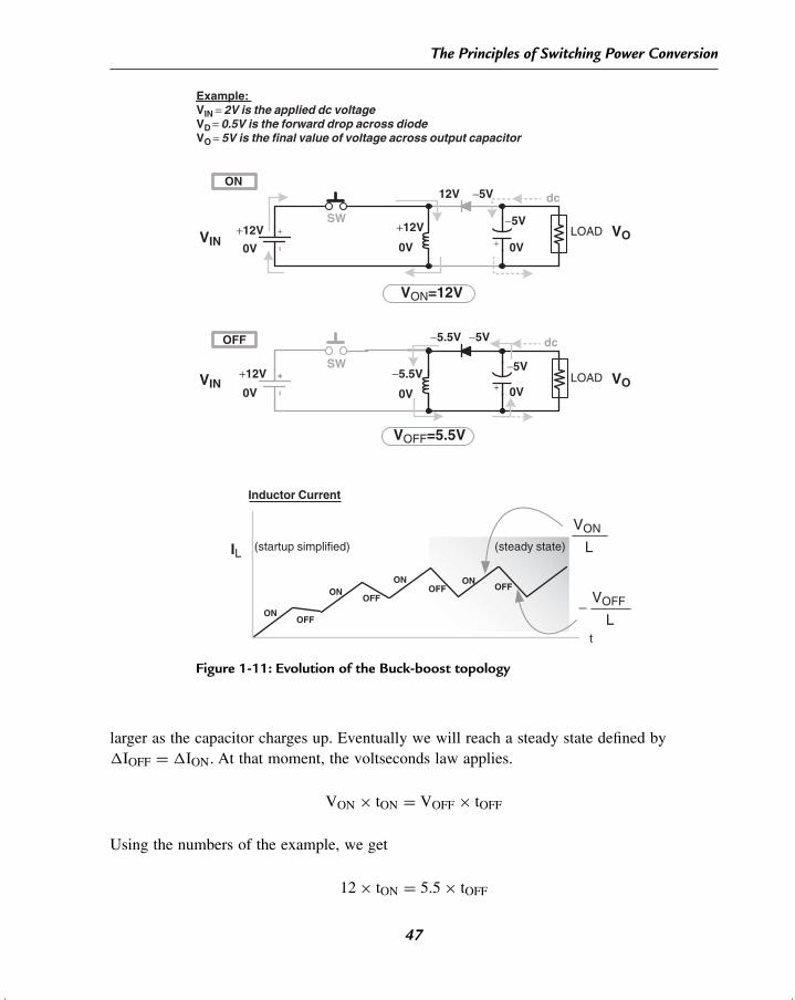
Typeset by: CEPHA Imaging Pvt. Ltd., INDIA
[17:36 2006/4/19 Chap-01.tex] MANIKTALA: Switching Power Supplies A to Z Page: 47 1–60
The Principles of Switching Power Conversion
−+
−+ +12V
0V
0V0V
+12V
+12V
0V
−5V
−5V
−5V−5.5V
−5.5V−5V
12V
VIN
VIN
IL
+
+
0V
0V
LOAD
LOAD VO
VO
ON
OFF
Example:VIN = 2V is the applied dc voltageVD = 0.5V is the forward drop across diodeVO = 5V is the final value of voltage across output capacitor
SW
SW
dc
dc
VON=12V
VOFF=5.5V
t
ON
ONON
OFFOFFOFF
OFF
ON
Inductor Current
(startup simplified) (steady state)
L
VOFF
L
VON
−
Figure 1-11: Evolution of the Buck-boost topology
larger as the capacitor charges up. Eventually we will reach a steady state defined by∆IOFF = ∆ION. At that moment, the voltseconds law applies.
VON × tON = VOFF × tOFF
Using the numbers of the example, we get
12 × tON = 5.5 × tOFF
47
Typeset by: CEPHA Imaging Pvt. Ltd., INDIA
[17:36 2006/4/19 Chap-01.tex] MANIKTALA: Switching Power Supplies A to Z Page: 48 1–60
Chapter 1
We see that a 5 V output is possible only if we have been switching with a constant ratiobetween the switch ON and switch OFF time, as given by
tOFF
tON= 12
5.5= 2.18
So to get the voltseconds to balance out for this case (5 V output and a 12 V input), we haveto make the off-time 2.18 times larger than the on-time. Why so? Simply because the voltageduring the on-time (across the inductor) is larger by exactly the same proportion: 12 V duringthe on-time as compared to 5.5 V during the off-time. Check: 12/5.5 = 2.18.
The duty cycle (assuming CCM) is therefore equal to
D = tON
tON + tOFF= 1
1 + tOFFtON
= 1
1 + 2.18= 0.314
Now, had we taken a semiconductor switch instead of a mechanical one, we would have hada non-zero forward voltage drop, of say “VSW”. This forward drop effectively just subtractsfrom the applied dc input during the on-time. So, had we done the above calculationssymbolically, we would get
VON = VIN − VSW (Buck-boost)
and
VOFF = VO + VD (Buck-boost)
Then, from the voltseconds law
tOFF
tON= VIN − VSW
VO + VD(Buck-boost)
We thus get the duty cycle
D = VO + VD
VIN − VSW + VO + VD(Buck-boost)
If the switch and diode drops are small as compared to the input and output rails, we cansimply write
D ≈ VO
VIN + VO(Buck-boost)
48
Typeset by: CEPHA Imaging Pvt. Ltd., INDIA
[17:36 2006/4/19 Chap-01.tex] MANIKTALA: Switching Power Supplies A to Z Page: 49 1–60
The Principles of Switching Power Conversion
We can also write the relationship between the input and output as follows
VO = VIN × D
1 − D(Buck-boost)
Note that some other easily derivable, and convenient relationships to remember are
tON
tOFF= D
1 − D(any topology)
tON = D
f(any topology)
tOFF = 1 − D
f≡ D′
f(any topology)
where we have defined D′ = 1 − D as the ‘duty cycle of the diode’, since the diode isconducting for the remainder of the switching cycle duration (in CCM).
Ground-Referencing Our Circuits
We need to clearly establish what is referred to as the ‘ground’ rail in any dc-dc switchingtopology. We know that there are two rails by which we apply the dc input voltage (currentgoes in from one and returns from the other). Similarly, there are also two output rails. Butall practical topologies generally have one rail that is common to both the input and theoutput. It is this common rail, that by convention, is called the system ‘ground’ in dc-dcconverter applications.
However, there is yet another convention in place — the ground is also considered to be“0 V” (zero volts).
The Buck-Boost Configurations
In Figure 1-12 the common (ground) rails have been highlighted in bold gray background.
We now realize that the buck-boost we presented in Figure 1-11 is actually a ‘positive(input) to negative (output)’ buck-boost. There is another possibility, as shown in the lowerhalf of Figure 1-12. We have re-labeled its ground in accordance with the normalconvention. Therefore this is a ‘negative to positive buck-boost’.
For either configuration, we see that whatever polarity is present at the input, it gets reversedat the output. Therefore, the buck-boost is often simply called an ‘inverting’ topology (thoughwe should keep in mind that that allows for two different configurations).
49
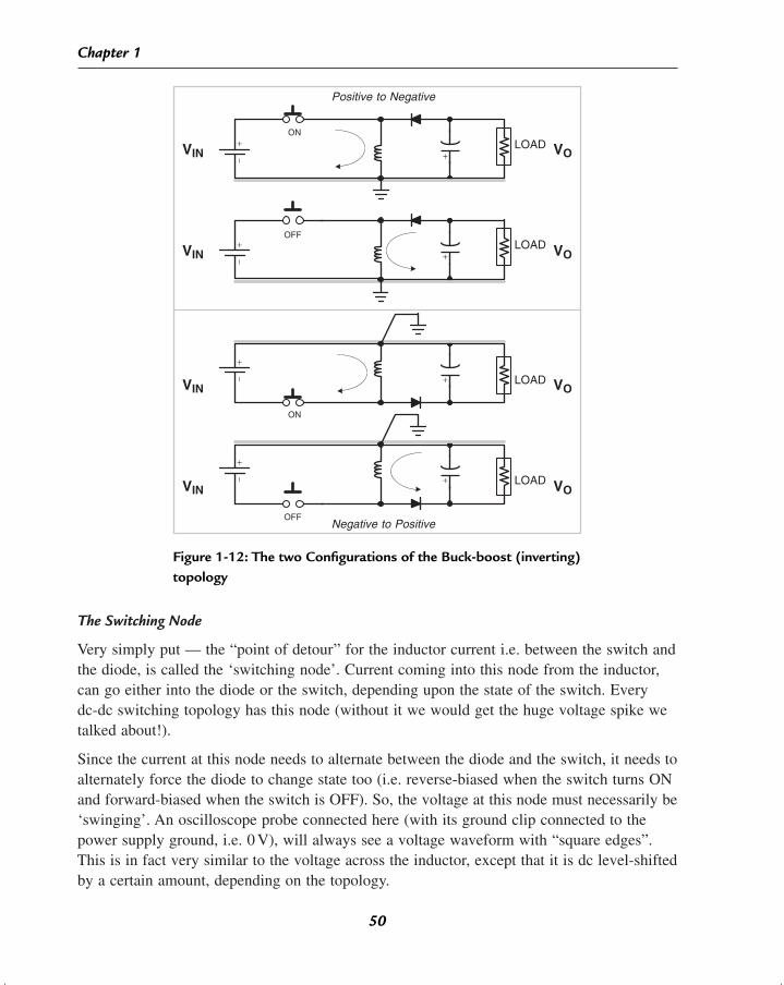
Typeset by: CEPHA Imaging Pvt. Ltd., INDIA
[17:36 2006/4/19 Chap-01.tex] MANIKTALA: Switching Power Supplies A to Z Page: 50 1–60
Chapter 1
−+
VIN +
LOAD VO
−+
VIN +
LOAD VO
VINLOAD VO
VINLOAD VO
−+
+
−+
+
ON
OFF
ON
OFF
Positive to Negative
Negative to Positive
Figure 1-12: The two Configurations of the Buck-boost (inverting)topology
The Switching Node
Very simply put — the “point of detour” for the inductor current i.e. between the switch andthe diode, is called the ‘switching node’. Current coming into this node from the inductor,can go either into the diode or the switch, depending upon the state of the switch. Everydc-dc switching topology has this node (without it we would get the huge voltage spike wetalked about!).
Since the current at this node needs to alternate between the diode and the switch, it needs toalternately force the diode to change state too (i.e. reverse-biased when the switch turns ONand forward-biased when the switch is OFF). So, the voltage at this node must necessarily be‘swinging’. An oscilloscope probe connected here (with its ground clip connected to thepower supply ground, i.e. 0 V), will always see a voltage waveform with “square edges”.This is in fact very similar to the voltage across the inductor, except that it is dc level-shiftedby a certain amount, depending on the topology.
50
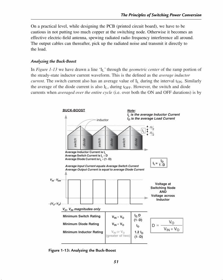
Typeset by: CEPHA Imaging Pvt. Ltd., INDIA
[17:36 2006/4/19 Chap-01.tex] MANIKTALA: Switching Power Supplies A to Z Page: 51 1–60
The Principles of Switching Power Conversion
On a practical level, while designing the PCB (printed circuit board), we have to becautious in not putting too much copper at the switching node. Otherwise it becomes aneffective electric-field antenna, spewing radiated radio frequency interference all around.The output cables can thereafter, pick up the radiated noise and transmit it directly tothe load.
Analyzing the Buck-Boost
In Figure 1-13 we have drawn a line ‘IL’ through the geometric center of the ramp portion ofthe steady-state inductor current waveform. This is the defined as the average inductorcurrent. The switch current also has an average value of IL during the interval tON. Similarlythe average of the diode current is also IL, during tOFF. However, the switch and diodecurrents when averaged over the entire cycle (i.e. over both the ON and OFF durations) is by
inductor
switc
h
diod
e
switc
h
diod
e
switc
h
diod
e
2∆I
2∆I
IL
−(VO+VD)
VIN −VSW
Voltage atSwitching Node
ANDVoltage across
Inductor
Average Inductor Current is ILAverage Switch Current is IL × DAverage Diode Current is IL × (1−D)
Average Input Current equals Average Switch CurrentAverage Output Current is equal to average Diode Current
IL=IO
1−D
Note:IL is the average Inductor CurrentIO is the average Load Current
BUCK-BOOST
Minimum Switch Rating
Minimum Diode Rating
Minimum Inductor Rating
VIN + VO
VIN + VO
IO D
IO
1.2 IO
(1−D)
(1−D)
VIN or VO(greater of two)
VIN + VO
VOD =
VO, VIN magnitudes only
Figure 1-13: Analyzing the Buck-Boost
51
Typeset by: CEPHA Imaging Pvt. Ltd., INDIA
[17:36 2006/4/19 Chap-01.tex] MANIKTALA: Switching Power Supplies A to Z Page: 52 1–60
Chapter 1
simple mathematics their respective weighted averages.
ISW_AVG = IL × tON
T= IL × D (Buck-boost)
ID_AVG = IL × tOFF
T= IL × D′ = IL × (
1 − D)
(Buck-boost)
where D′ is the duty cycle of the diode, i.e. 1 − D. It is also easy to visualize that for thisparticular topology, the average input current is equal to the average switch current. Further,as we will see below, the average diode current is equal to the load current. This is whatmakes the buck-boost topology quite different from the buck topology.
Properties of the Buck-Boost
We now make some observations based on Figure 1-11, Figure 1-12 and Figure 1-13
For example, a “positive to negative” buck-boost can convert 12 V to −5 V (stepdown) or 12 V to −15 V (step up). A “negative to positive” buck-boost can convertsay −12 V to 5 V or 5 V to 15 V, and so on. The magnitude of the output voltagecan thus be either smaller or larger (or equal to) the magnitude of the input voltage.
When the switch is ON, energy is delivered only into the inductor by the input dcsource (via the switch), and none of it passes through to the output.
When the switch is OFF, only the stored energy of the inductor is pushed into theoutput (through the diode), and none comes directly from the input dc source.
The above two observations make the buck-boost topology the only “pure flyback”topology around, in the sense that all the energy transferred from the input to theoutput, must have been previously stored in the inductor. No other topology sharesthis unique property.
The current coming from the input capacitor (dc source) is “choppy” i.e. pulsating.That is because, this current, combined with the steady dc current (IIN) coming infrom the dc source, basically forms the switch current waveform (which we know isalways choppy for any topology) (see Figure 1-9).
Similarly, the current into the output capacitor is also choppy, because combinedwith the steady dc current into the load (IOUT), it forms the diode current (which weknow is always choppy for any topology) (see Figure 1-9).
We know that heat dissipation is proportional to the square of the RMS current. Andsince choppy waveforms have high RMS values, the efficiency of a buck-boost is notvery good. Also, there is generally a relatively high level of noise and ripple across
52
Typeset by: CEPHA Imaging Pvt. Ltd., INDIA
[17:36 2006/4/19 Chap-01.tex] MANIKTALA: Switching Power Supplies A to Z Page: 53 1–60
The Principles of Switching Power Conversion
the board. Therefore, the buck-boost may also demand much better filtering at itsinput, and often at its output too.
Though current enters the output capacitor to charge it up when the switch turns ON,and leaves it to go into the load when the switch is OFF, the average capacitorcurrent is always zero. In fact, any capacitor in ‘steady-state’, must, by definition,have zero average current passing through it — otherwise it would keep charging ordischarging until it too reaches a steady state, just like the inductor current.
Since the average current from the output capacitor is zero, therefore, for thebuck-boost, the average diode current must be equal to the load current (where elsecan the current come from?). Therefore
ID_AVG = IO = IL × (1 − D
)
So,
IL = IO
1 − D(Buck-boost)
This is the relationship between the average inductor current and the load current. Notethat in Figure 1-13, in the embedded table, we have asked for an inductor rated for1.2 × IO/(1 − D). The factor “1.2” comes from the fact, that by typical design criteria, thepeak of the inductor current waveform is about 20% higher than its average. So we need tolook for an inductor rated at least for a current of 1.2 × IL.
Why Three Basic Topologies Only?
There are certainly several ways to set up circuits using an inductor, which provide a“freewheeling path” too, for the inductor current. But some of these are usually disqualifiedsimply because the input and output do not share a common rail, and thus there is no properground reference available for the converter and the rest of the system. Two examples ofsuch “working-but-unacceptable” converters are the buck-boost configurations shown inFigure 1-14. Compare these with Figure 1-12 to see what the problem is! However, note thatif these were “front-end converters”, the system ground could be established starting at theoutput of this converter itself, and may thus be acceptable.
Of the remaining ways, several are just “configurations” of a basic topology (like the twoconfigurations in Figure 1-12). Among the basic topologies, we actually have just three —the buck, the boost, and the buck-boost. Why only three? That is because of the way theinductor is connected. Note that with proper ground-referencing in place, there are only threedistinct rails possible — the input, the output, and the (common) ground. So if one end ofthe inductor is connected to the ground, it becomes a buck-boost! On the other hand, if it is
53
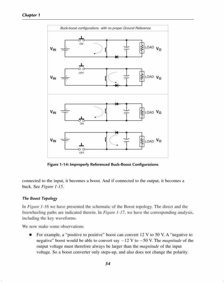
Typeset by: CEPHA Imaging Pvt. Ltd., INDIA
[17:36 2006/4/19 Chap-01.tex] MANIKTALA: Switching Power Supplies A to Z Page: 54 1–60
Chapter 1
−+
VIN +
LOAD
LOAD
LOAD
LOAD
VO
VIN VO
VIN VO
VIN VO
−+
+
−+
+
−+
+
ON
OFF
ON
OFF
Buck-boost configurations with no proper Ground Reference
Figure 1-14: Improperly Referenced Buck-Boost Configurations
connected to the input, it becomes a boost. And if connected to the output, it becomes abuck. See Figure 1-15.
The Boost Topology
In Figure 1-16 we have presented the schematic of the Boost topology. The direct and thefreewheeling paths are indicated therein. In Figure 1-17, we have the corresponding analysis,including the key waveforms.
We now make some observations
For example, a “positive to positive” boost can convert 12 V to 50 V. A “negative tonegative” boost would be able to convert say −12 V to −50 V. The magnitude of theoutput voltage must therefore always be larger than the magnitude of the inputvoltage. So a boost converter only steps-up, and also does not change the polarity.
54
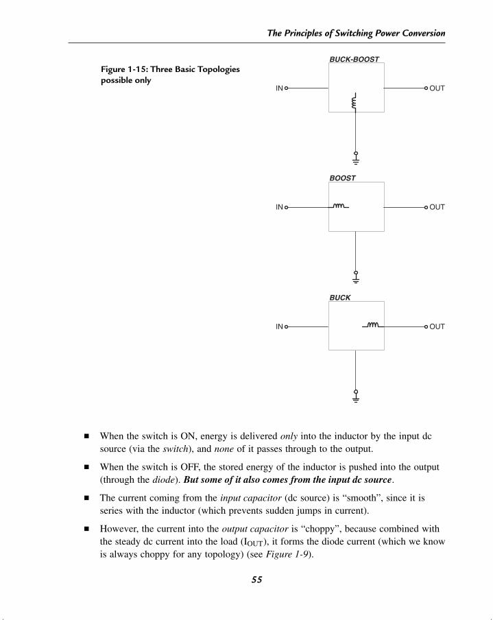
Typeset by: CEPHA Imaging Pvt. Ltd., INDIA
[17:36 2006/4/19 Chap-01.tex] MANIKTALA: Switching Power Supplies A to Z Page: 55 1–60
The Principles of Switching Power Conversion
Figure 1-15: Three Basic Topologiespossible only
IN OUT
OUT
OUT
BUCK-BOOST
IN
BOOST
IN
BUCK
When the switch is ON, energy is delivered only into the inductor by the input dcsource (via the switch), and none of it passes through to the output.
When the switch is OFF, the stored energy of the inductor is pushed into the output(through the diode). But some of it also comes from the input dc source.
The current coming from the input capacitor (dc source) is “smooth”, since it isseries with the inductor (which prevents sudden jumps in current).
However, the current into the output capacitor is “choppy”, because combined withthe steady dc current into the load (IOUT), it forms the diode current (which we knowis always choppy for any topology) (see Figure 1-9).
55
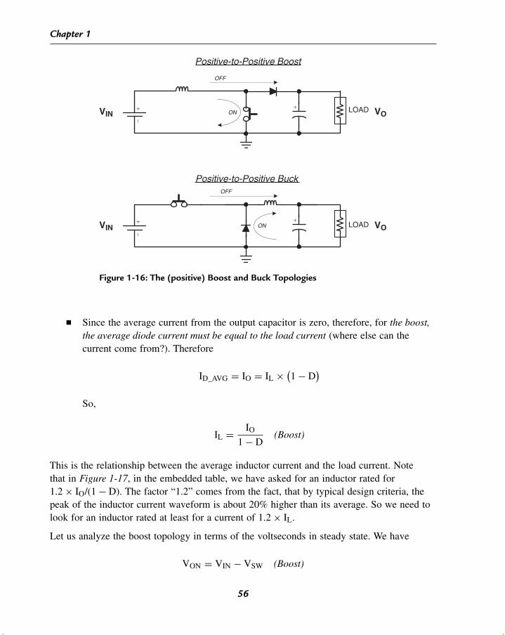
Typeset by: CEPHA Imaging Pvt. Ltd., INDIA
[17:36 2006/4/19 Chap-01.tex] MANIKTALA: Switching Power Supplies A to Z Page: 56 1–60
Chapter 1
−+ +
LOAD
LOAD
VO
VO
VIN
VIN −+ +
Positive-to-Positive Boost
OFF
OFF
Positive-to-Positive Buck
ON
ON
Figure 1-16: The (positive) Boost and Buck Topologies
Since the average current from the output capacitor is zero, therefore, for the boost,the average diode current must be equal to the load current (where else can thecurrent come from?). Therefore
ID_AVG = IO = IL × (1 − D
)
So,
IL = IO
1 − D(Boost)
This is the relationship between the average inductor current and the load current. Notethat in Figure 1-17, in the embedded table, we have asked for an inductor rated for1.2 × IO/(1 − D). The factor “1.2” comes from the fact, that by typical design criteria, thepeak of the inductor current waveform is about 20% higher than its average. So we need tolook for an inductor rated at least for a current of 1.2 × IL.
Let us analyze the boost topology in terms of the voltseconds in steady state. We have
VON = VIN − VSW (Boost)
56
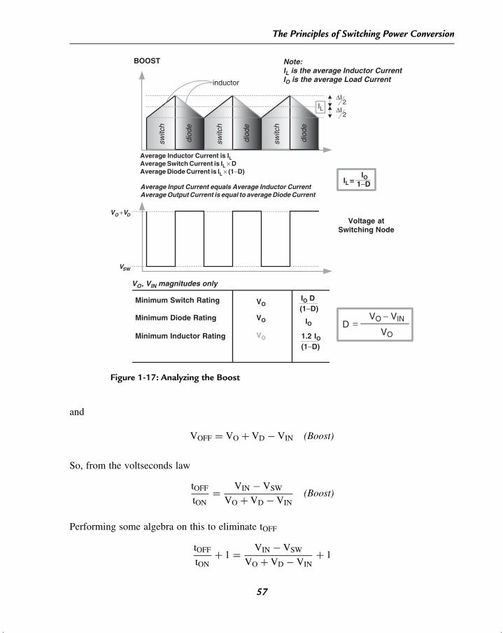
Typeset by: CEPHA Imaging Pvt. Ltd., INDIA
[17:36 2006/4/19 Chap-01.tex] MANIKTALA: Switching Power Supplies A to Z Page: 57 1–60
The Principles of Switching Power Conversion
inductor
Voltage atSwitching Node
Average Input Current equals Average Inductor CurrentAverage Output Current is equal to average Diode Current
BOOST
Minimum Switch Rating
Minimum Diode Rating
Minimum Inductor Rating
VO
VO
VO
switc
h
diod
e
switc
h
diod
e
switc
h
diod
e
2∆I
2∆IIL
IL=IO
1−D
IO D
IO
1.2 IO
(1−D)
(1−D)
VO, VIN magnitudes only
Average Inductor Current is ILAverage Switch Current is IL × DAverage Diode Current is IL × (1−D)
Note:IL is the average Inductor CurrentIO is the average Load Current
VO +VD
VSW
VO
VO − VIND =
Figure 1-17: Analyzing the Boost
and
VOFF = VO + VD − VIN (Boost)
So, from the voltseconds law
tOFF
tON= VIN − VSW
VO + VD − VIN(Boost)
Performing some algebra on this to eliminate tOFF
tOFF
tON+ 1 = VIN − VSW
VO + VD − VIN+ 1
57
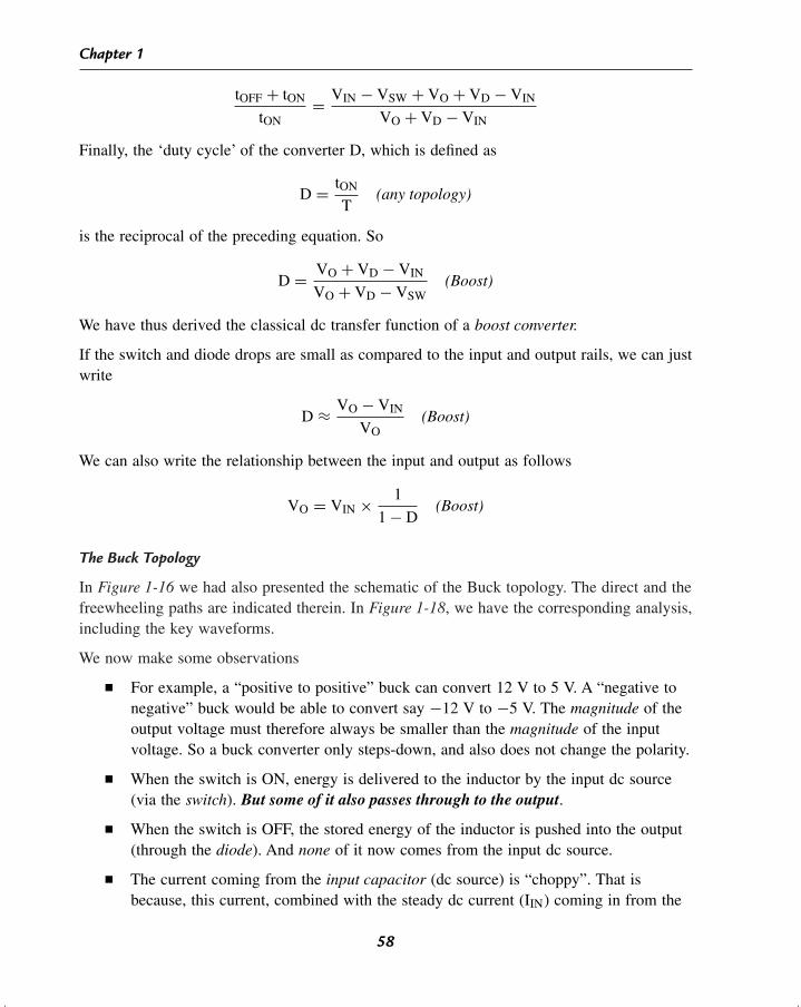
Typeset by: CEPHA Imaging Pvt. Ltd., INDIA
[17:36 2006/4/19 Chap-01.tex] MANIKTALA: Switching Power Supplies A to Z Page: 58 1–60
Chapter 1
tOFF + tON
tON= VIN − VSW + VO + VD − VIN
VO + VD − VIN
Finally, the ‘duty cycle’ of the converter D, which is defined as
D = tON
T(any topology)
is the reciprocal of the preceding equation. So
D = VO + VD − VIN
VO + VD − VSW(Boost)
We have thus derived the classical dc transfer function of a boost converter.
If the switch and diode drops are small as compared to the input and output rails, we can justwrite
D ≈ VO − VIN
VO(Boost)
We can also write the relationship between the input and output as follows
VO = VIN × 1
1 − D(Boost)
The Buck Topology
In Figure 1-16 we had also presented the schematic of the Buck topology. The direct and thefreewheeling paths are indicated therein. In Figure 1-18, we have the corresponding analysis,including the key waveforms.
We now make some observations
For example, a “positive to positive” buck can convert 12 V to 5 V. A “negative tonegative” buck would be able to convert say −12 V to −5 V. The magnitude of theoutput voltage must therefore always be smaller than the magnitude of the inputvoltage. So a buck converter only steps-down, and also does not change the polarity.
When the switch is ON, energy is delivered to the inductor by the input dc source(via the switch). But some of it also passes through to the output.
When the switch is OFF, the stored energy of the inductor is pushed into the output(through the diode). And none of it now comes from the input dc source.
The current coming from the input capacitor (dc source) is “choppy”. That isbecause, this current, combined with the steady dc current (IIN) coming in from the
58
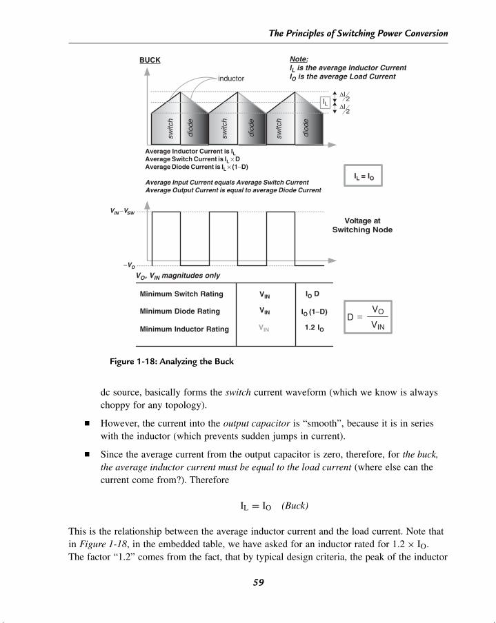
Typeset by: CEPHA Imaging Pvt. Ltd., INDIA
[17:36 2006/4/19 Chap-01.tex] MANIKTALA: Switching Power Supplies A to Z Page: 59 1–60
The Principles of Switching Power Conversion
Voltage atSwitching Node
BUCK
inductor
switc
h
diod
e
switc
h
diod
e
switc
h
diod
e
2∆I
2∆I
IL
−VD
VIN −VSW
Average Inductor Current is ILAverage Switch Current is IL × DAverage Diode Current is IL × (1−D)
Average Input Current equals Average Switch CurrentAverage Output Current is equal to average Diode Current
IL = IO
Note:IL is the average Inductor CurrentIO is the average Load Current
Minimum Switch Rating
Minimum Diode Rating
Minimum Inductor Rating
VIN
VIN
IO D
IO (1−D)
1.2 IOVIN VIN
VOD =
VO, VIN magnitudes only
Figure 1-18: Analyzing the Buck
dc source, basically forms the switch current waveform (which we know is alwayschoppy for any topology).
However, the current into the output capacitor is “smooth”, because it is in serieswith the inductor (which prevents sudden jumps in current).
Since the average current from the output capacitor is zero, therefore, for the buck,the average inductor current must be equal to the load current (where else can thecurrent come from?). Therefore
IL = IO (Buck)
This is the relationship between the average inductor current and the load current. Note thatin Figure 1-18, in the embedded table, we have asked for an inductor rated for 1.2 × IO.The factor “1.2” comes from the fact, that by typical design criteria, the peak of the inductor
59
Typeset by: CEPHA Imaging Pvt. Ltd., INDIA
[17:36 2006/4/19 Chap-01.tex] MANIKTALA: Switching Power Supplies A to Z Page: 60 1–60
Chapter 1
current waveform is about 20% higher than its average. So we need to look for an inductorrated at least for a current of 1.2 × IL.
Let us analyze the buck topology in terms of the voltseconds in steady state. We have
VON = VIN − VSW − VO (Buck)
and
VOFF = VO − (−VD) = VO + VD (Buck)
As before, using the voltseconds law and simplifying, we get the ‘duty cycle’ of the converter
D = VO + VD
VIN + VD − VSW(Buck)
We have thus derived the classical dc transfer function of a buck converter. If the switch anddiode drops are small as compared to the input and output rails, we can just write
D ≈ VO
VIN(Buck)
We can also write the relationship between the input and output as follows
VO = VIN × D (Buck)
Advanced Converter Design
This should serve as an introduction to understanding and designing switching powerconverters. More details and worked examples can be found in the next Chapter (titled“DC-DC Converter Design and Magnetics”). The reader can also at this point briefly scanChapter 4 for some finer nuances of design. A full design table is also available inAppendix 2 for future reference.
60
Related Documents


![[Ravazi]Principles of Data Conversion System Design](https://static.cupdf.com/doc/110x72/577c7dd11a28abe0549ff5d4/ravaziprinciples-of-data-conversion-system-design.jpg)