Abstract The Light at the End of the Tunnel Junction - Improving the Energy Resolution of UV Single-Photon Spectrometers using Diffusion Engineering Veronica Andreea Savu Yale University 2007 We present experimental results which test whether diffusion engineering can increase the energy resolution of a single-photon superconducting tunnel-junction spectrometer. When a UV photon is absorbed in superconducting Al, it creates an excess number of quasiparticles. If the superconducting absorber is the electrode of a tunnel junction, the quasiparticles tunnel across the voltage-biased junction. The collected charge is propor- tional to the number of excess quasiparticles. For small energy photons, the initially- created charge can be amplified by backtunnelling. The quasiparticles confined around the junction can backtunnel as holes after tunnelling, doubling the output charge, and then tunnel again. The charge multiplication is proportional to the confinement time. When the counterelectrode is terminated with a long, narrow lead, the quasiparticles diffuse out on a time scale set by the dimensions of the leads and of the electrodes, and the diffusion con- stant of the material. We show how the charge created by the photon varies with the purity of the Al film and with different lead geometries. The experimental results are compared to theoretical predictions of our model. We achieve an energy resolving power of 3 for a photon energy of 3.68 eV. Further investigation of losses in our materials should improve the energy resolution of our diffusion-engineered devices.

Welcome message from author
This document is posted to help you gain knowledge. Please leave a comment to let me know what you think about it! Share it to your friends and learn new things together.
Transcript
Abstract
The Light at the End of the Tunnel Junction - Improving the Energy
Resolution of UV Single-Photon Spectrometers using Diffusion
Engineering
Veronica Andreea Savu
Yale University
2007
We present experimental results which test whether diffusion engineering can increase
the energy resolution of a single-photon superconducting tunnel-junction spectrometer.
When a UV photon is absorbed in superconducting Al, it creates an excess number of
quasiparticles. If the superconducting absorber is the electrode of a tunnel junction, the
quasiparticles tunnel across the voltage-biased junction. The collected charge is propor-
tional to the number of excess quasiparticles. For small energy photons, the initially-
created charge can be amplified by backtunnelling. The quasiparticles confined around
the junction can backtunnel as holes after tunnelling, doubling the output charge, and then
tunnel again. The charge multiplication is proportional to the confinement time. When the
counterelectrode is terminated with a long, narrow lead, the quasiparticles diffuse out on a
time scale set by the dimensions of the leads and of the electrodes, and the diffusion con-
stant of the material. We show how the charge created by the photon varies with the purity
of the Al film and with different lead geometries. The experimental results are compared
to theoretical predictions of our model. We achieve an energy resolving power of 3 for a
photon energy of 3.68 eV. Further investigation of losses in our materials should improve
the energy resolution of our diffusion-engineered devices.

2

The Light at the End of the Tunnel Junction - Improving theEnergy Resolution of UV Single-Photon Spectrometers using
Diffusion Engineering
A Dissertation
Presented to the Faculty of the Graduate School
of
Yale University
in Candidacy for the Degree of
Doctor of Philosophy
by
Veronica Andreea Savu
Dissertation Director: Professor Daniel E. Prober
May 2007

Table of Contents
1 Introduction 1
1.1 Overview . . . . . . . . . . . . . . . . . . . . . . . . . . . . . . . . . . 1
1.2 Operating Principle of the Detector . . . . . . . . . . . . . . . . . . . . . 2
1.3 Previous Group Research and Concurrent Work . . . . . . . . . . . . . . 8
1.4 Thesis Organization . . . . . . . . . . . . . . . . . . . . . . . . . . . . . 10
2 Theory 12
2.1 Intrinsic Quasiparticle Non-equilibrium Processes . . . . . . . . . . . . . 12
2.1.1 Quasiparticle Generation . . . . . . . . . . . . . . . . . . . . . . 12
2.1.2 Quasiparticle Tunnelling . . . . . . . . . . . . . . . . . . . . . . 15
2.1.3 Quasiparticle Recombination . . . . . . . . . . . . . . . . . . . . 18
2.2 Diffusion Engineering . . . . . . . . . . . . . . . . . . . . . . . . . . . . 21
2.2.1 Diffusion . . . . . . . . . . . . . . . . . . . . . . . . . . . . . . 22
2.2.2 Simple Analytical Model . . . . . . . . . . . . . . . . . . . . . . 24
2.2.3 Electrical Equivalent . . . . . . . . . . . . . . . . . . . . . . . . 26
2.2.4 Diffusion Simulation . . . . . . . . . . . . . . . . . . . . . . . . 26
2.3 Diffusion Engineering Flowchart . . . . . . . . . . . . . . . . . . . . . . 31
3 Experimental Setup 35
3.1 Overview . . . . . . . . . . . . . . . . . . . . . . . . . . . . . . . . . . 35
3.2 Cryogenics . . . . . . . . . . . . . . . . . . . . . . . . . . . . . . . . . 36
3.3 Electronics . . . . . . . . . . . . . . . . . . . . . . . . . . . . . . . . . 37
i

3.3.1 Electrical Contacts . . . . . . . . . . . . . . . . . . . . . . . . . 37
3.3.2 DC Electronics . . . . . . . . . . . . . . . . . . . . . . . . . . . 39
3.3.3 AC Electronics . . . . . . . . . . . . . . . . . . . . . . . . . . . 40
3.3.4 Magnetic Field . . . . . . . . . . . . . . . . . . . . . . . . . . . 41
3.4 Shielding . . . . . . . . . . . . . . . . . . . . . . . . . . . . . . . . . . 42
3.5 Optics . . . . . . . . . . . . . . . . . . . . . . . . . . . . . . . . . . . . 43
3.6 Data Acquisition . . . . . . . . . . . . . . . . . . . . . . . . . . . . . . 44
4 Fabrication 45
4.1 Overview . . . . . . . . . . . . . . . . . . . . . . . . . . . . . . . . . . 45
4.2 Ta Deposition . . . . . . . . . . . . . . . . . . . . . . . . . . . . . . . . 48
4.3 Ta Ion-Milling . . . . . . . . . . . . . . . . . . . . . . . . . . . . . . . . 48
4.4 Au Deposition . . . . . . . . . . . . . . . . . . . . . . . . . . . . . . . . 48
4.5 Junction Fabrication . . . . . . . . . . . . . . . . . . . . . . . . . . . . . 49
4.6 Device Layout . . . . . . . . . . . . . . . . . . . . . . . . . . . . . . . . 52
4.6.1 Design Files . . . . . . . . . . . . . . . . . . . . . . . . . . . . 52
4.6.2 Device Imaging . . . . . . . . . . . . . . . . . . . . . . . . . . . 55
5 Experimental Results 57
5.1 Research Path . . . . . . . . . . . . . . . . . . . . . . . . . . . . . . . . 57
5.1.1 Ta-absorber Devices . . . . . . . . . . . . . . . . . . . . . . . . 58
5.1.2 Al-absorber Devices . . . . . . . . . . . . . . . . . . . . . . . . 59
5.2 Dilution Refrigerator Measurements . . . . . . . . . . . . . . . . . . . . 60
5.3 Device Response to UV Photons . . . . . . . . . . . . . . . . . . . . . . 65
5.3.1 Ideal Poisson Distribution of Photons . . . . . . . . . . . . . . . 65
5.3.2 Diffusion in Al . . . . . . . . . . . . . . . . . . . . . . . . . . . 67
5.3.3 Aluminum Devices with ∆ = 170 µeV (Chip1) . . . . . . . . . . 69
5.3.4 Aluminum Devices with ∆ = 225 µeV (Chip2) . . . . . . . . . . 71
ii

5.3.5 Aluminum Devices with ∆ = 235 µeV (Chip3) . . . . . . . . . . 74
5.3.6 Charge Multiplication . . . . . . . . . . . . . . . . . . . . . . . 75
5.4 Summary . . . . . . . . . . . . . . . . . . . . . . . . . . . . . . . . . . 76
6 Conclusions 82
6.1 Diffusion Engineering Review . . . . . . . . . . . . . . . . . . . . . . . 82
6.2 Device Performance . . . . . . . . . . . . . . . . . . . . . . . . . . . . . 83
6.3 Alternative Future Approaches . . . . . . . . . . . . . . . . . . . . . . . 83
Appendices 85
A Film Properties 85
B Device Parameters 87
Bibliography 88
iii

List of Figures
1.1 Simulated current vs. voltage characteristic (using the BCS theory) of an
STJ with unsuppressed Cooper pair current. . . . . . . . . . . . . . . . . 3
1.2 Current vs. voltage characteristic of an STJ with suppressed Cooper pair
current. . . . . . . . . . . . . . . . . . . . . . . . . . . . . . . . . . . . 3
1.3 An absorbed photon in one electrode of an STJ creates excess quasiparti-
cles that tunnel across the voltage-biased junction, recorded as a current
pulse. . . . . . . . . . . . . . . . . . . . . . . . . . . . . . . . . . . . . 4
1.4 Energy band diagram of a junction in a modified excitation representation. 7
1.5 Energy band diagram of a junction with a higher-gap material plug on the
left side, in the modified excitation representation. . . . . . . . . . . . . . 8
2.1 Quasiparticle energy Ek and ξk as a function of the free electron energy
relative to the Fermi energy. . . . . . . . . . . . . . . . . . . . . . . . . 14
2.2 Different tunnelling processes shown in the modified excitation represen-
tation. . . . . . . . . . . . . . . . . . . . . . . . . . . . . . . . . . . . . 16
2.3 Quasiparticle density as a function of temperature for materials with dif-
ferent energy gaps. . . . . . . . . . . . . . . . . . . . . . . . . . . . . . 19
2.4 Recombination time as a function of temperature for different values of
the energy gap ∆. . . . . . . . . . . . . . . . . . . . . . . . . . . . . . . 20
2.5 Energy diagram for devices employing different intrinsic charge multipli-
cation techniques. . . . . . . . . . . . . . . . . . . . . . . . . . . . . . . 22
iv

2.6 Time evolution of a Gaussian function subject to diffusion and center of
mass motion. . . . . . . . . . . . . . . . . . . . . . . . . . . . . . . . . 23
2.7 Geometry of the counter-electrode and out-diffusion lead in our detectors. 24
2.8 Linear quasiparticle concentration profile in the wire. . . . . . . . . . . . 25
2.9 Electrical circuit model for a diffusion-engineered device. . . . . . . . . . 27
2.10 Dirichlet and Neumann boundary conditions set on our domain. . . . . . 27
2.11 Evolution in time of the quasiparticle concentration in the counter-electrode
and lead. . . . . . . . . . . . . . . . . . . . . . . . . . . . . . . . . . . . 29
2.12 Variation of the time for the concentration profile in the wire to become
linear with diffusion constant. . . . . . . . . . . . . . . . . . . . . . . . 30
2.13 Fit with a slope of 1 for times up to 20 µs of the simulation time versus the
time calculated with the linear regime analytical formula. . . . . . . . . . 31
2.14 Diffusion engineering flowchart reflecting the different connections be-
tween device parameters. . . . . . . . . . . . . . . . . . . . . . . . . . . 32
3.1 Experimental setup. . . . . . . . . . . . . . . . . . . . . . . . . . . . . . 36
3.2 Circuit board with Cu traces and wire-bonded devices on a chip, along
with the quasi-Helmzoltz coils used to produce a parallel magnetic field. . 38
3.3 Active voltage biasing electronics, with the cross indicating our device. . 42
4.1 The Dolan-bridge patterning technique [not to scale]. . . . . . . . . . . . 50
4.2 Cross-sectional view of the Dolan-bridge double-angle evaporation tech-
nique [not to scale]. . . . . . . . . . . . . . . . . . . . . . . . . . . . . . 51
4.3 Layout of resist pattern for the Ta layer. . . . . . . . . . . . . . . . . . . 54
4.4 Layout of resist pattern for the Au and Al layers. . . . . . . . . . . . . . 55
4.5 Optical micrograph of Chip2 excluding part of the leads at a magnification
of 500. . . . . . . . . . . . . . . . . . . . . . . . . . . . . . . . . . . . 56
4.6 SEM pictures of devices. . . . . . . . . . . . . . . . . . . . . . . . . . . 56
v

5.1 Sketches of different device generation design [not to scale]. The scale is
set by all the junctions being 1×5 µm2. . . . . . . . . . . . . . . . . . . 60
5.2 Consecutive device geometry generations. . . . . . . . . . . . . . . . . . 61
5.3 Optical micrograph of sample B−C2−T F . . . . . . . . . . . . . . . . . 62
5.4 Measured I(V) curve at different magnetic field values, at 46 mK. . . . . 62
5.5 The energy gap measured as a function of magnetic field at 46 mK. . . . . 63
5.6 Measured critical current versus applied parallel magnetic field at 46 mK. 63
5.7 Measured subgap current and the associated theoretical BCS curves for
different temperatures. . . . . . . . . . . . . . . . . . . . . . . . . . . . 64
5.8 Measured subgap current versus temperature. . . . . . . . . . . . . . . . 64
5.9 Ideal Poisson distribution of photons with an average number of photons
of 0.5. . . . . . . . . . . . . . . . . . . . . . . . . . . . . . . . . . . . . 65
5.10 Non-ideal detection of an ideal Poisson distribution of photons with an
average number of photons of 0.5. . . . . . . . . . . . . . . . . . . . . . 67
5.11 Diffusion constant D and resistivity ρ as a function of oxygen flow during
Al deposition. . . . . . . . . . . . . . . . . . . . . . . . . . . . . . . . . 68
5.12 Current vs. voltage characteristic of the ∆ = 170 µeV devices. . . . . . . . 70
5.13 Pulse histograms for the clean Al, long diffusion-engineered device, tested
at different light intensities, each corresponding to a different average pho-
ton number of the Poisson distribution. . . . . . . . . . . . . . . . . . . . 71
5.14 FWHM of the energy distribution for the ∆ = 170 µeV devices. . . . . . . 72
5.15 Charge offset vs. average number of photons for the ∆ = 170 µeV devices. 73
5.16 Current vs. voltage characteristic of the ∆ = 225 µeV devices. . . . . . . . 73
5.17 Microscope slide with Au deposited on it (Au mirror). . . . . . . . . . . . 74
5.18 Pulse histograms from three different devices under laser testing. . . . . . 77
5.19 Charge offset Q0 vs. average number of photons N for the ∆ = 225 µeV
devices. . . . . . . . . . . . . . . . . . . . . . . . . . . . . . . . . . . . 78
vi

5.20 FWHM of the energy distribution for the ∆ = 225 µeV devices. . . . . . . 78
5.21 Violet photon single pulse and UV photons average pulse. . . . . . . . . 79
5.22 Current vs. voltage characteristic of the ∆ = 235 µeV devices. . . . . . . . 79
5.23 Charge offset vs. average number of photons for the ∆ = 235 µeV devices. 80
5.24 FWHM of the energy distribution for the ∆ = 235 µeV devices. . . . . . . 80
5.25 Results. . . . . . . . . . . . . . . . . . . . . . . . . . . . . . . . . . . . 81
vii

List of Tables
2.1 Tunnelling Processes . . . . . . . . . . . . . . . . . . . . . . . . . . . . 16
4.1 Resist process parameters for Ta . . . . . . . . . . . . . . . . . . . . . . 49
4.2 Parameters for Au deposition in the Plassys. . . . . . . . . . . . . . . . . 49
4.3 Resist process parameters for Al junctions. . . . . . . . . . . . . . . . . . 50
4.4 Parameters for Al deposition for junctions fabricated in the Plassys . . . 52
4.5 Parameters for Al film deposition and junction oxidation. . . . . . . . . . 52
5.1 Al film parameters as a function of the O2 concentration during evaporation. 68
5.2 Diffusion constants, effective temperature, and predicted outdiffusion times
for different devices. . . . . . . . . . . . . . . . . . . . . . . . . . . . . 75
A.1 Properties of Ta and Al films. . . . . . . . . . . . . . . . . . . . . . . . . 86
B.1 Device Parameters - the normal resistance was measured at voltages > 2∆
and at a temperature T << TC. . . . . . . . . . . . . . . . . . . . . . . . 87
B.2 Important Runs and Selected Results . . . . . . . . . . . . . . . . . . . . 87
viii

List of Symbols
∆ superconducting energy gap
∆E total energy resolution (measured at FWHM)
∆Eelec energy resolution due to electronic noise extrinsic to the device
∆Eelectrical energy resolution due to electrical noise
∆E f lux energy resolution due to photons absorbed outside the absober
∆EFano energy resolution due to F
∆Etunn energy resolution due to G
ε mean energy to produce a quasiparticle
Γ rate constant
Ω phonon energy
ΩD Debye phonon energy
σ conductivity
τ time constant
τout outdiffusion time
τtunn tunnelling time
A j junction area
c constant of proportionality
C capacitance
d Al thickness
ix

dox thickness of the junction oxide
dr1 thickness of the first resist layer
D diffusion constant
Dqp quasiparticle diffusion constant
e electron’s charge
e base of natural logarithm
eV electron volt
Ephoton photon energy
f(E) Fermi distribution function
E quasiparticle energy
Ek energy of quasiparticle with momentum ~k
F Fano factor
G factor representing the variation in the number of tunnellings for a quasiparticle
~ Planck’s constant divided by 2π
3He isotope of helium with atomic mass of 3
4He isotope of helium with atomic mass of 4
in current noise
Idc dc STJ quiescent current
IC critical current of the junction
jC junction critical current density
k wave vector
kB Boltzmann’s constant
kF Fermi wave vector
l outdiffusion lead length
L electrode length
m electron mass
M tunneling matrix element
x

n quasiparticle density
N quasiparticle number
p charge multiplication factor
Qi initial charge created by photon
Q0 offset charge
Rn resistance of STJ in normal state
R recombination constant
T temperature
TC critical temperature
w outdiffusion lead width
W electrode width
Vb bias voltage
Vol volume
xi

Acknowledgements
This dissertation was only possible with the help of many people. I would first like to thank
my advisor, Daniel E. Prober, for his support throughout my years of graduate school. His
teaching, experimental skills and intuition as a physicist provide a model I hope some
day to achieve. Luigi Frunzio has also provided extraordinary help and counsel since the
beginning of this project.
The other members of the Prober lab have contributed invaluably to my research. Chris
Wilson immersed me in the subtleties of the experiment, and set an excellent example for
me to follow. I am also indebted to Liqun Li for having patiently taught me the physics
of the project. I benefited from many technical discussions with Matt Reese and enjoyed
our countless hours together. Bertrand Reulet, the excellent physicist with whom I shared
lab space, brought warmth and wisdom. Daniel Santavicca and Anthony Annunziata were
fantastic colleagues who contributed to a stimulating intellectual atmosphere in Becton
405. Aviad Frydman and Misha Reznikov were great friends and mentors during their
year as members of the group. Stephan Friedrich and Ken Segall offered their insights and
experience at important moments during the project. Thanks also to the junior member of
our group, Joel Chudow, and to the two undergraduate students who assisted me during
summer research, Ivan Borzenets and Jonah Waissman.
I thank my dissertation committee members, Karyn Le Hur, Simon Mochrie, Robert
Schoelkopf, and Andrew Szymkowiak for their careful reading and insightful comments,
which have greatly strengthened the final version of the thesis. Caroline Kilbourne at God-
dard Space Flight Center, who served as the outside reader, gave me excellent feedback on
xii

a very tight schedule.
Many other members of the Yale faculty have contributed to my rich experience as
a graduate student. I received much useful advice regarding optics from Bob Grober. I
learned a lot from Kurt Gibble during the year I spent in his lab before he moved on to a
tenured position at Penn State. I learned how to be a better teacher from my interactions
with Michel Devoret, Peter Kindlmann, Ramamurti Shankar, Meg Urry, and Alex Zeller.
My professors at Caltech and Irina Calomfirescu, my Physics teacher at Mihai Viteazul
high-school in Bucharest, also contributed to my growth as a scientist.
The fourth floor of Becton was enlivened by many graduate students and postdocs,
from whom I have received help in innumerable ways, small and large: Aric Sanders,
Minghao Shen, Julie Love, John Teufel, Ben Turek, Vijay (a.k.a. Rajamani Vijayaragha-
van), Irfan Siddiqi, Mike Metcalfe, Hannes Majer, Andreas Walraff, Etienne Boaknin,
David Schuster, Lafe Spietz, Chad Rigetti, and Vladimir Manucharyan. I owe special
gratitude to the administrative staff for years of help and warm friendship: Maria Gubitosi,
Theresa Evangeliste, Jo-Ann Bonnett, and Jayne Miller.
I particularly enjoyed the friendship and support of the small group of exceptional
women with whom I started my studies in the Yale Physics Department in September
2000: Betty Bezverkhny Abelev, Sarah Bickman, Grace Chern, and Sevil Salur. Betty and
Veronica became so close that we have been immortalized in the popular culture with our
own comic strip and t-shirts. Sam Bench, one of the few other women on the fourth floor
of Becton, has been a friend since undergraduate days at Caltech. I am grateful for the
friendship of Stefania Marin, which added joy to my life in New Haven. The Romanian
community in New Haven has also been a constant source of support and comradery.
My mother and father, Maria Andreea and Nicusor Savu, gave all of themselves to
raising me. Though it has meant great distance from their only child for a decade, they
encouraged and supported me to pursue an independent career in the United States. My
husband, Martin Benjamin, who I met and married during my time at Yale, offered me a
xiii

tremendous amount of moral support and love. He put his linguistic experience to good
use by proofreading the first version of my dissertation. I dedicate this thesis to him and
to my parents.
xiv

Chapter 1
Introduction
1.1 Overview
Superconducting tunnel junctions (STJs) have been used for over a decade as single
photon spectrometers. The gap energy in superconductors is on the order of 1 meV, three
orders of magnitude smaller than in semiconductors. Thus, for the same energy photon
absorbed, there are many more excitations created in a superconductor than in a semicon-
ductor. This offers the potential for better energy resolution using superconductors instead
of the conventional semiconductors. A further advantage of superconductors is that their
typical Debye energies (tens of meV), which are a measure of the maximum phonon en-
ergy, are much larger than their energy gaps. Thus, the phonons generated by an absorbed
photon participate in the creation of excess excitations. These advantages led to a sus-
tained effort in the photon detector community. The detectors were initially developed for
X-ray photons. Most of the experiments used the Mn Kα and Kβ lines of a 55Fe source,
with an energy of 5.89 keV and 6.49 keV. In 1986 Twerenbold and colleagues achieved
an energy resolution of 65 eV at 6 keV with Sn tunnel junctions [Twerenbold1986]. As
the energy resolution for X-rays improved, the STJ-based detectors have been developed
for lower-energy photons, all the way from soft X-rays down into the near infrared (NIR)
range.
Astronomy has already benefitted from the use of STJ-based single photon spectrome-
1

ters [Bruijne2002]. The photon’s energy (color) as well as its arrival time can be recorded,
at a relatively high counting rate. Thus, transient weak signals from distant sources can be
explored, such as visible light from pulsars and variable stars. The change in brightness
of several spectral channels can be recorded in parallel, on millisecond to microsecond
timescales [Rando2000].
In biology, measurement of fluorescent spectra at the single-photon level is a chal-
lenging issue [Nagl2005]. For imaging low intensity fluorescent specimens, avalanche
photodiodes (APDs) are usually used. For obtaining spectral information, an APD has to
be used with a set of narrow-band filters. Every time the band filter is changed, one can
record data at a specific wavelength. For studying multiple chromophores, the sample has
to be scanned multiple times, increasing its probability of photobleaching. On the other
hand, dispersive gratings have as many as 32 energy channels [LSM510], but they are read
sequentially with only one photomultiplier tube (PMT). Simultaneous read-out of all the
channels would require a high level of experimental complexity.
The development of ultra-sensitive, fast spectrometers for single UV and optical pho-
tons would benefit many applications from a wide range of research fields. In addition
to this practical goal, improving the modelling of the physical processes inside the STJ-
based detectors should deepen our understanding of the basic physics of non-equilibrium
quasiparticle processes in superconductors.
1.2 Operating Principle of the Detector
Our detectors have two main functional parts: a superconducting absorber and a super-
conducting tunnel junction. For the work presented in this thesis, the role of the absorber
is played by the Al electrodes of an Al/Al-oxide/Al junction. In a Josephson junction
there is a maximum Cooper pair tunneling current, called the supercurrent or the critical
current IC. For larger currents a voltage develops across the junction. Figure 1.1 shows
2

the current vs. voltage characteristic of a Josephson tunnel junction with the Cooper pair
current. In our experiments, the Cooper pair tunnel current must be suppressed in order
to enable stable voltage biasing of the junction [Friedrich97IEEE]. We suppress the pair
tunnel current by applying a magnetic field parallel to the plane of the junction. We apply
a bias voltage and monitor the current due to the thermally excited quasiparticles tunneling
across the junction. This quiescent current decreases exponentially with the inverse of the
temperature. Figure 1.2 shows the simulated thermal current in a device for two different
bath temperatures, after the critical current has been totally suppressed, a zoom-in around
the origin of Figure 1.1 without the critical current branch.
I
V2∆/e
IC
Figure 1.1: Simulated current vs. voltage characteristic (using the BCS theory) of an STJwith unsuppressed Cooper pair current.
-5
0
5
I [n
A]
-150 -100 -50 0 50 100 150V [µV]
T = 300 mK T = 360 mK
Figure 1.2: Current vs. voltage characteristic of an STJ with suppressed Cooper paircurrent.
3
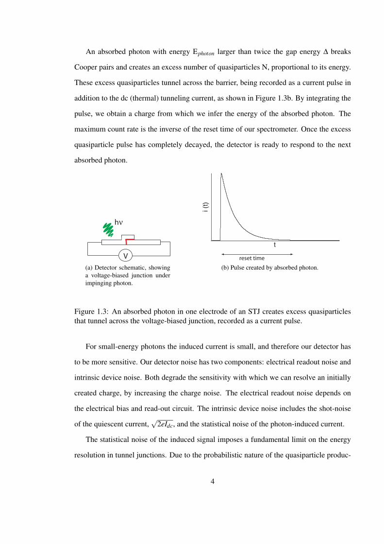
An absorbed photon with energy Ephoton larger than twice the gap energy ∆ breaks
Cooper pairs and creates an excess number of quasiparticles N, proportional to its energy.
These excess quasiparticles tunnel across the barrier, being recorded as a current pulse in
addition to the dc (thermal) tunneling current, as shown in Figure 1.3b. By integrating the
pulse, we obtain a charge from which we infer the energy of the absorbed photon. The
maximum count rate is the inverse of the reset time of our spectrometer. Once the excess
quasiparticle pulse has completely decayed, the detector is ready to respond to the next
absorbed photon.
V
hν
(a) Detector schematic, showinga voltage-biased junction underimpinging photon.
i (t
)
t
reset time
(b) Pulse created by absorbed photon.
Figure 1.3: An absorbed photon in one electrode of an STJ creates excess quasiparticlesthat tunnel across the voltage-biased junction, recorded as a current pulse.
For small-energy photons the induced current is small, and therefore our detector has
to be more sensitive. Our detector noise has two components: electrical readout noise and
intrinsic device noise. Both degrade the sensitivity with which we can resolve an initially
created charge, by increasing the charge noise. The electrical readout noise depends on
the electrical bias and read-out circuit. The intrinsic device noise includes the shot-noise
of the quiescent current,√
2eIdc, and the statistical noise of the photon-induced current.
The statistical noise of the induced signal imposes a fundamental limit on the energy
resolution in tunnel junctions. Due to the probabilistic nature of the quasiparticle produc-
4
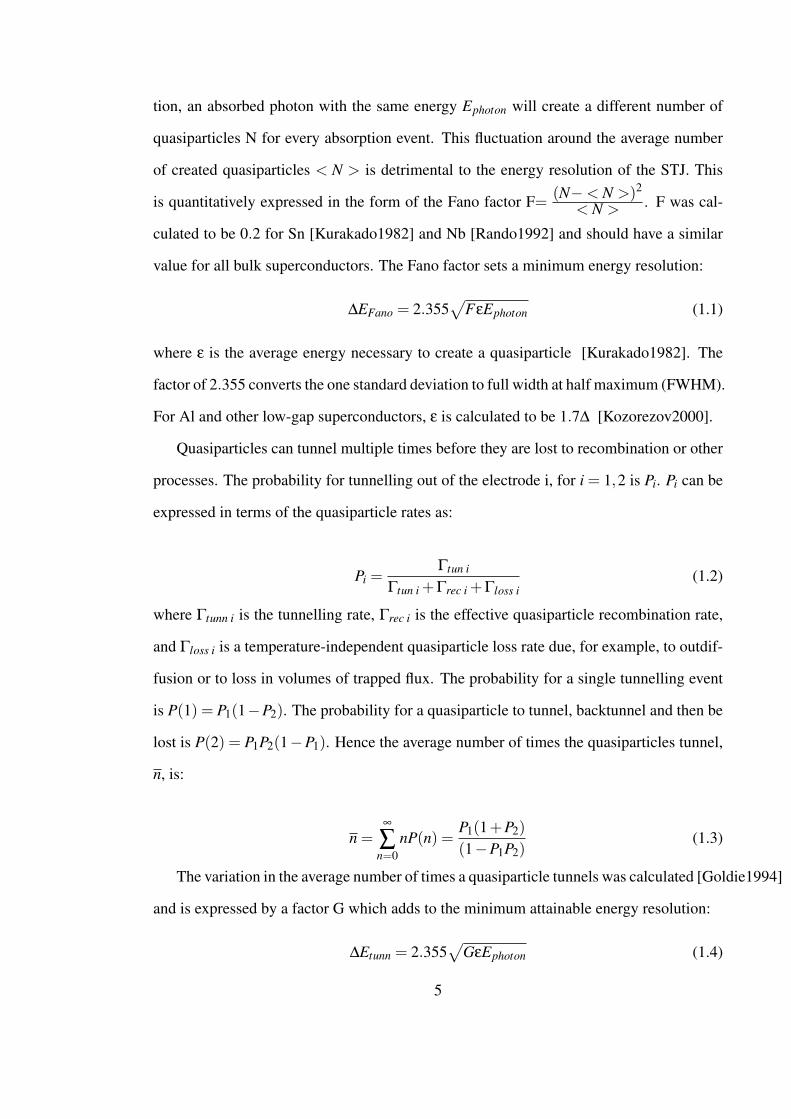
tion, an absorbed photon with the same energy Ephoton will create a different number of
quasiparticles N for every absorption event. This fluctuation around the average number
of created quasiparticles < N > is detrimental to the energy resolution of the STJ. This
is quantitatively expressed in the form of the Fano factor F= (N−< N >)2
< N > . F was cal-
culated to be 0.2 for Sn [Kurakado1982] and Nb [Rando1992] and should have a similar
value for all bulk superconductors. The Fano factor sets a minimum energy resolution:
∆EFano = 2.355√
FεEphoton (1.1)
where ε is the average energy necessary to create a quasiparticle [Kurakado1982]. The
factor of 2.355 converts the one standard deviation to full width at half maximum (FWHM).
For Al and other low-gap superconductors, ε is calculated to be 1.7∆ [Kozorezov2000].
Quasiparticles can tunnel multiple times before they are lost to recombination or other
processes. The probability for tunnelling out of the electrode i, for i = 1,2 is Pi. Pi can be
expressed in terms of the quasiparticle rates as:
Pi =Γtun i
Γtun i +Γrec i +Γloss i(1.2)
where Γtunn i is the tunnelling rate, Γrec i is the effective quasiparticle recombination rate,
and Γloss i is a temperature-independent quasiparticle loss rate due, for example, to outdif-
fusion or to loss in volumes of trapped flux. The probability for a single tunnelling event
is P(1) = P1(1−P2). The probability for a quasiparticle to tunnel, backtunnel and then be
lost is P(2) = P1P2(1−P1). Hence the average number of times the quasiparticles tunnel,
n, is:
n =∞
∑n=0
nP(n) =P1(1+P2)(1−P1P2)
(1.3)
The variation in the average number of times a quasiparticle tunnels was calculated [Goldie1994]
and is expressed by a factor G which adds to the minimum attainable energy resolution:
∆Etunn = 2.355√
GεEphoton (1.4)
5

For our devices, G is computed to be of order unity.
The total energy resolution due to the quasiparticle statistical processes adds in quadra-
ture with the energy resolution imposed by other electrical noise sources ∆Eelectrical:
∆Etot =√
∆E2Fano +∆E2
tunn +∆E2electrical (1.5)
Both F and G represent statistical noise sources which set a limit on detecting low-
energy photons with good energy resolving power (Ephoton/∆E). However, in an STJ there
is a remarkable process which allows intrinsic charge multiplication, effectively increasing
the signal created by a photon. A quasiparticle is a linear superposition of an electron and
a hole. As shown in Figure 1.4, it can tunnel as an electron from electrode 1 to electrode
2, and it can backtunnel as a hole from electrode 2 to electrode 1, in both cases gaining
energy eVb from the bias voltage Vb. This one quasiparticle transfers two negative charges
from left to right, such that the measured number of electrons exceeds the initial excess
quasiparticle number Qi/e. This is the ‘Gray effect’ [Gray1978], also known as backtun-
nelling. The same quasiparticle can continue tunnelling and backtunnelling, increasing the
detected charge, pQi, until it either recombines or diffuses away from the junction area.
The charge multiplication factor p is the ratio of the residence time of the quasiparticles in
the electrodes to the tunnelling time.
Previous research in our group studied devices with a large multiplication factor, p
≈ 50. This was achieved by confining the quasiparticles with higher-gap materials on
each side of the electrodes. This ‘gap-engineering’ approach introduced Joule heating in
our junctions. In a single-tunnelling junction, once the quasiparticles tunnel, they quickly
diffuse away from the junction into wide leads. In the gap-engineered devices, the quasi-
particles keep tunnelling and backtunnelling, until they are lost through recombination.
Upon tunnelling they gain energy from the bias voltage. They scatter inelastically by
emitting phonons, thus relaxing down in energy. The scattering time decreases with the
cube of the initial energy, such that quasiparticles of energy 4∆ take several nanoseconds
6

12
electrode 1 electrode 2
eV b
∆
Figure 1.4: Energy band diagram of a junction in a modified excitation representation.The arrows illustrate quasiparticle tunnelling events. The quasiparticles tunnel as electronsfrom left to right, gaining the bias energy | eVb |, as showed by the darker arrow in process1. They backtunnel as holes from right to left, gaining the bias energy | eVb |, as showedby the grey arrow in process 2.
to emit a phonon [Segall2004]. Not all of them relax down to the energy gap level be-
fore they backtunnel. After multiple tunnellings, some of the quasiparticles have energies
larger than 3∆. These can generate excess quasiparticles by emission of 2∆ or larger
phonons. These phonons break pairs and cause an increase in the dc current, like heating.
This effect was seen in our gap-engineered devices, increasing the shot current noise in
our measurement.
In the case of STJ-based spectrometers which use larger-gap leads on each side of the
junction to promote backtunnelling, there is an additional noise source which limits the
energy resolution [Wilson2001]. This is the thermal generation-recombination noise, due
to the thermodynamic fluctuations of the quiescent quasiparticle number in the electrodes.
Implementing a moderate charge multiplication factor could reach an optimum signal-
to-noise ratio. The signal would increase according to the charge multiplication factor,
without too much heating. The present research tested this hypothesis by using diffusion-
engineered devices. The quasiparticles are confined in the left electrode by the higher-gap
material, tantalum (Ta), which acts like a plug, in the same way as in the gap-engineered
devices, as seen in Figure 1.5. The right electrode is continued with a long, narrow lead,
made from the same material as the electrodes. We expect the energy resolution of this
7

device type to be limited only by the statistical noise sources. The quasiparticle residence
time here is dictated by the time it takes them to diffuse out the narrow lead, called the
out-diffusion time. The out-diffusion time is a function of the material diffusion constant,
the lead dimensions, and its relative size compared to the electrode size. By changing the
wire geometry, we can control the out-diffusion time. This allows us to test regimes with
different charge multiplication factors by implementing different lead designs.
12
electrode 1 electrode 2
eV b
∆plug
∆‘
Figure 1.5: Energy band diagram of a junction with a higher-gap material plug on the leftside, in the modified excitation representation.
1.3 Previous Group Research and Concurrent Work
Michael Gaidis [Gaidis1994] started the work on STJ detectors at Yale. He developed
the initial design, fabrication process, electrical characterization and testing of high quality
STJ detectors for X-ray photons. Using a charge pulse amplifier, he obtained an energy
resolution of 190 eV for 6 keV X-rays.
Stephan Friedrich [Friedrich1997] tested double-junction devices for X-rays, achiev-
ing spatial resolution for the absorbed photon in the absorber. He constructed a lower-
noise, more stable electronic circuit. When combined with the imaging detectors, the
energy resolution reached 54 eV at 6 keV. The new current pulse amplifier allowed for
extraction of relevant quasiparticle time scales.
Kenneth Segall [Segall2000] further improved the electronics and experimental setup,
while developing a detailed microscopic model for the detectors. An energy resolution of
8

26 eV at 6 keV was achieved. Quantifying all the device noise sources and developing the
microscopic model were an important step towards developing a better detector.
Liqun Li [Li2002] continued testing of X-ray imaging devices, using improved designs
and lowering the electronic noise even more. From device physics studies, the diffusion
constant and quaisparticle lifetime in the Ta absorber were extracted. It was her work that
triggered the idea of implementing controlled outdiffusion for increasing backtunnelling
in our devices: X-ray data showed a slower than expected pulse decay time for a device
connected through a narrow lead to the wiring pads. The best energy resolution was 13 eV
at 6 keV.
Christopher Wilson [Wilson2002] tested both imaging and single-junction optical de-
tectors. He developed a detailed model that relates the thermodynamic fluctuations in the
junction electrodes to the device excess current noise. From thorough modelling and anal-
ysis of the backtunnelling device data, his conclusion was that having less backtunnelling
could alleviate the self-heating effect present in the strong backtunnelling devices. The
strong backtunnelling, double-junction detector exhibited a very good energy resolution
of 1.5 eV at 4.89 eV over the whole 10×100 µm2 Ta absorber, when tested with photons
from a Hg lamp. For the non-backtunnelling devices tested with laser pulses, the electronic
noise ∆Eelectrical was 2.14 eV. The total noise ∆E was fit by adding the electronic noise
in quadrature with ∆E f lux extra noise due to the photon flux, ∆E =√
(∆E2elec + N∆E2
f lux).
The extra noise ∆E f lux was found to be 1.3 eV per absorbed photon. The laser photons
had an energy of 3.68 eV.
The European Space Agency (ESA) developed a 12× 10 pixel array of STJs, called
S-Cam 3, for ground-based astronomy, deployed at the 4.2 m William Herschel telescope
in La Palma, Spain. The devices use a stack geometry with Ta/Al electrodes. The photon
is absorbed in the Ta layer. The excess created quasiparticles diffuse into the Al electrode,
where they are trapped by energy relaxation. They tunnel and backtunnelling multiple
times across the Al/Al-oxide/Al junction, increasing the collected charge. They are con-
9
fined around the junction area because of the higher-gap Ta ‘plugs’. The measured resolv-
ing power averaged over all the channels was 10 at 2.48 eV [Verhoeve2006] for a pulse
time of 20 µs.
1.4 Thesis Organization
In this thesis we present the work done on developing high energy resolution single
UV photon detectors based on Al/Al-oxide/Al STJs using diffusion engineering.
Chapter 2 introduces the basic device physics. The concept of diffusion engineering
is explained. We start with a simple, intuitive analytical model and describe its electrical
equivalent. A more complex simulation of the diffusion process is presented and we com-
pare it to the simpler model. Using a diffusion engineering flowchart, we comment on the
requirements necessary for maximizing our device signal-to-noise ratio, which leads to
competing trends for certain parameters. We show how we optimized the values for these
parameters.
Chapter 3 describes the experimental setup, including cryogenics, electronics, electro-
magnetic shielding, optics and data acquisition procedures.
Chapter 4 explains in detail the fabrication techniques and parameters used for making
the devices tested in this thesis. The main 3-layer processing is presented in an easy to
understand, non-chronological order: first the resist processes for each layer, followed by
the metal deposition steps for each layer. The device layout is explained and optical and
electron-beam pictures of relevant devices are included.
Chapter 5 presents the research path followed in this work. The present research started
with the development of a new STJ fabrication technique, necessary for reaching the re-
quirements for this project. The different device generations and the reasoning behind
the changes in their design and fabrication are reviewed. Results from the most relevant
devices are presented and analyzed.
In Chapter 6 we discuss the performance of our devices and the main obstacles en-
10

countered. We suggest alternative approaches for future work on detector development.
The Appendices provide additional information regarding experimental film proper-
ties, device parameters, and a summary of the experimental results.
11

Chapter 2
Theory
2.1 Intrinsic Quasiparticle Non-equilibrium Processes
2.1.1 Quasiparticle Generation
Radiation detectors consist of an absorber and a readout. The energy deposited in the
absorber is converted into excitations. These are registered by the readout which outputs
a signal proportional to the amount of deposited energy. In the energy range for which the
detector is designed, the absorber must be efficient in absorbing radiation and transferring
the resulting excitations to the readout. In our STJ spectrometer, the main absorbers are
the superconducting Al electrodes and the readout is the superconducting tunnel junction.
The impinging photon deposits its energy in the absorber, where it is converted into excess
phonons and quasiparticles. The excess quasiparticles tunnel across the voltage-biased
junction, creating a pulse of current. We integrate the pulse and obtain the total charge
that tunnelled. By calibrating the detector with photons of known energy, we determine
the transfer function between the incident energy and the output charge. We can then use
the transfer function for doing spectrometry on photons of unknown energy within the
calibrated range.
The choice of the absorber material depends on the energy range of the photons. We
want the material to be mainly absorbing, instead of being reflective or transparent, in
that energy range. In this work we are developing spectrometers for detecting photons in
12

the optical / UV range. A very good choice in this range is Ta, which has a reflectivity
around 40% in the 2−12 eV range for a thick sample [Weaver1974] (to avoid transmission
of photons through the material). This means that approximately 60% of the incoming
photons are absorbed, the rest being reflected.
The absorber is in its superconducting state. In a superconducting metal, electrons
with opposite wave vectors (k, -k) and opposite spins (↑, ↓) are bound into pairs known
as Cooper pairs. The Cooper pairs form a condensate which is the BCS superconducting
ground state [BCS1957]. Excitations of the superconducting ground state, called quasipar-
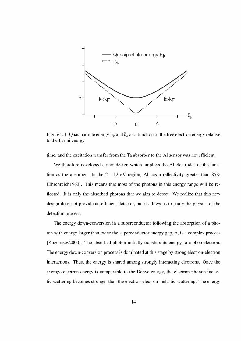
ticles, were calculated in 1958 by Bogoliubov and Valatin. The energy Ek of a quasipar-
ticle with momentum ~k is Ek =√
ξ2k +∆2. Here ξk is the energy of a free electron with
momentum ~k relative to the Fermi energy EF , thus ξk = ~2k2
2m −EF . Figure 2.1 shows
the quasiparticle energy as a function of free electron energy. There are two quasiparti-
cle branches: the hole-like quasiparticles (k< kF ) and the electron-like quasiparticles (k>
kF ). Each excitation is a superposition of a hole-like and electron-like quasiparticle. When
a photon of energy larger than twice the energy gap, 2∆, is absorbed in a superconductor,
it breaks Cooper pairs and creates quasiparticle excitations.
The absorber must transfer the excitations to the tunnel junction quickly and efficiently
(without losses). Previous work in our group showed this is possible with a clean Ta / Al
interface [Gaidis1994]. The quasiparticles created in the Ta absorber then get ‘trapped’ in
the lower-energy gap Al, and they tunnel across the junction. The trapping time is due to
inelastic scattering of quasiparticles with phonon emission. For energies E that are large
compared to the energy gap ∆, the scattering rate is proportional to(
E∆
)3. Quasiparticles
with energies higher than 3∆Al scatter down to lower energies in several tens of nanosec-
onds [Segall2000]. As long as the size of the Al trap is large enough that the diffusion
time inside it is greater than the inelastic scattering time, the quasiparticles will not diffuse
back to the Ta. Due to the different fabrication technique of our devices, the diffusion time
from the Ta absorber into the Al trap in our first designs was comparable to the trapping
13
∆−∆ 0
∆
Quasiparticle energy |ξk|
ξk
Ek
k>kFk<kF
Figure 2.1: Quasiparticle energy Ek and ξk as a function of the free electron energy relativeto the Fermi energy.
time, and the excitation transfer from the Ta absorber to the Al sensor was not efficient.
We therefore developed a new design which employs the Al electrodes of the junc-
tion as the absorber. In the 2− 12 eV region, Al has a reflectivity greater than 85%
[Ehrenreich1963]. This means that most of the photons in this energy range will be re-
flected. It is only the absorbed photons that we aim to detect. We realize that this new
design does not provide an efficient detector, but it allows us to study the physics of the
detection process.
The energy down-conversion in a superconductor following the absorption of a pho-
ton with energy larger than twice the superconductor energy gap, ∆, is a complex process
[Kozorezov2000]. The absorbed photon initially transfers its energy to a photoelectron.
The energy down-conversion process is dominated at this stage by strong electron-electron
interactions. Thus, the energy is shared among strongly interacting electrons. Once the
average electron energy is comparable to the Debye energy, the electron-phonon inelas-
tic scattering becomes stronger than the electron-electron inelastic scattering. The energy
14

down-conversion process releases a large number of phonons, which in turn excite more
quasiparticles. A phonon of energy Ω > 2∆ breaks one Cooper pair and creates two quasi-
particles. A quasiparticle of energy E > 3∆ can emit phonons of energy Ω > 2∆. Phonons
of energy Ω < 2∆ cannot break a Cooper pair, and quasiparticles with energy E < 3∆ can-
not emit phonons with energies Ω > 2∆, so neither contribute to the increase of the number
of excess quasiparticles.
The mean energy ε needed to produce an excess quasiparticle [Kurakado1982] in Al
is ε = 1.7∆ [Kozorezov2000], for an incident radiation with energy larger than several eV.
This means that 60% of the absorbed photon energy goes into the quasiparticle system,
while the remaining goes into phonons with energies below 2∆. In a superconductor the
gap energy ∆ (of order meV) is much smaller than the Debye energy ~ωD (tens of meV).
The high characteristic energy of the phonons relative to the energy gap 2∆ plays an im-
portant role in the efficient transfer of energy from an absorbed photon to quasiparticle
excitations. The phonons have enough energy to break Cooper pairs and generate excess
quasiparticles, so that ε is not much larger than ∆. This is unlike in semiconductors, where
the photon creates a single electron-hole excitation.
2.1.2 Quasiparticle Tunnelling
If we bias the junction with a bias voltage Vb, the quasiparticles will either tunnel
directly, with an energy gain eVb, or will reverse tunnel, losing eVb of energy. The di-
rect tunnelling processes allow quasiparticles to tunnel as electrons from left to right, or
as holes from right to left (backtunnelling), as depicted in Figure 2.2. The reverse tun-
nelling processes allow quasiparticles to tunnel as holes from left to right, or as electrons
from right to left. Table 2.1 shows the charge transfer for all the four processes. Refer-
ence [Tinkham1972] provides a clear description in terms of the BCS theory.
We can compute the tunnelling current and tunnelling rates associated with each of
these processes [Golubov1994] using a simplifying approximation. We assume that the
15
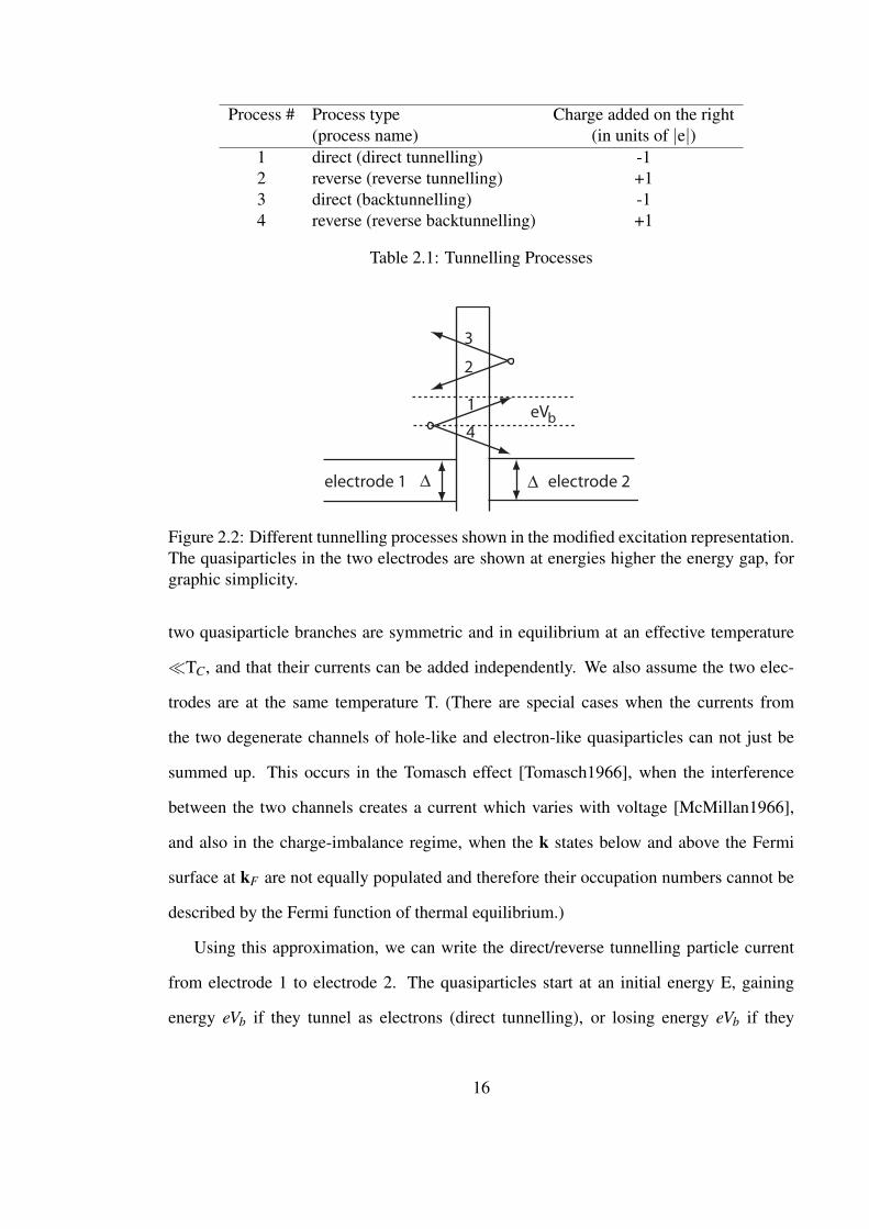
Process # Process type Charge added on the right(process name) (in units of |e|)
1 direct (direct tunnelling) -12 reverse (reverse tunnelling) +13 direct (backtunnelling) -14 reverse (reverse backtunnelling) +1
Table 2.1: Tunnelling Processes
1
2
3
4
electrode 1 electrode 2
eV b
∆∆
Figure 2.2: Different tunnelling processes shown in the modified excitation representation.The quasiparticles in the two electrodes are shown at energies higher the energy gap, forgraphic simplicity.
two quasiparticle branches are symmetric and in equilibrium at an effective temperature
¿TC, and that their currents can be added independently. We also assume the two elec-
trodes are at the same temperature T. (There are special cases when the currents from
the two degenerate channels of hole-like and electron-like quasiparticles can not just be
summed up. This occurs in the Tomasch effect [Tomasch1966], when the interference
between the two channels creates a current which varies with voltage [McMillan1966],
and also in the charge-imbalance regime, when the k states below and above the Fermi
surface at kF are not equally populated and therefore their occupation numbers cannot be
described by the Fermi function of thermal equilibrium.)
Using this approximation, we can write the direct/reverse tunnelling particle current
from electrode 1 to electrode 2. The quasiparticles start at an initial energy E, gaining
energy eVb if they tunnel as electrons (direct tunnelling), or losing energy eVb if they
16

tunnel as holes (reverse backtunnelling):
I1→2(E → E± eVb) =2π~|M | 2N1(E) f1(E)N2(E± eVb)[1− f2(E± eVb)] (2.1)
where M is the tunnelling matrix element between the two states, N(E) is the superconduct-
ing density of states, and f(E) is the Fermi function. The number of occupied initial quasi-
particle states in electrode 1 is N1(E) f1. The quasiparticles can only tunnel into the empty
states at the respective energies from the second electrode, N2(E± eVb)[1− f2(E± eVb)].
The tunnelling times can be computed from the tunnelling current:
τ−1tunn1→2(E → E± eVb) =
I1→2(E → E± eVb)N1(E) f1(E)
(2.2)
where N1(E) f1(E) is the number of quasiparticles available to tunnel from the first elec-
trode.
To compute the total tunnelling current, one has to integrate (2.1) over the available
energy range of E. We assume that the density of states in a normal metal is constant within
millielectronvolts (meV) of the Fermi energy, which is on the order of a few electronvolts
(eV). The superconducting density of states then is:
N1,2(E) =
Nn(0)E√E2−∆2
E > ∆
0 E < ∆(2.3)
where Nn(0) is the normal metal density of states at the Fermi level and ∆ is the supercon-
ducting energy gap.
The total electrical tunnelling current is computed as the sum of all the tunnelling
processes in the junction, considering the sign of the charge transferred (Table 2.1). The
direct tunnelling and the backtunelling processes contribute positive currents, while the
reverse tunnelling and the reverse backtunnelling contribute negative currents. Promoting
direct backtunnelling is a technique first used by N. E. Booth [Booth1987] to increase the
effective charge created by a photon.
Ielectricaldc = Idirect
1→2 − Ireverse1→2 + Ibacktunnel
2→1 − Irevbacktunnel2→1 (2.4)
17

In the low temperature limit kBT ¿ ∆ and in the subgap biasing region eV < 2∆, the
subgap current is estimated to be [VanDuzer1981]:
Ielectricaldc =
2(eV +∆)Rn
e−∆/kBT
√2∆
eV +2∆sinh
(eV
2kBT
)K0
(eV
2kBT
)(2.5)
where Rn is the normal state resistance of the junction, and K0 is the zeroth-order modified
Bessel Function.
The quasiparticle tunnelling times for direct/reverse processes taking them from an
energy E in the first electrode to an energy E± eV in the second electrode are:
τtunn1→2 = 2e2Nn(0)RnVol1
√(E± eV )2−∆2
E± eV(2.6)
where Vol1 is the volume of the electrode the quasiparticles are tunnelling from.
For the normal state, the times corresponding to an electron tunnelling from electrode
1 to 2 is:
τtunn1→2 = e2Nn(0)RnVol1 (2.7)
2.1.3 Quasiparticle Recombination
If quasiparticles get lost before tunnelling, they do not contribute to the signal and
the detector energy resolution is degraded. An important loss mechanism is quasiparticle
recombination. The number of ways N quasiparticles can be paired up is 12N(N − 1),
which in the case of a large N can be approximated by N2
2 .
We define R to be the recombination rate per unit density of quasiparticles. Since each
recombination event removes 2 quasiparticles, the recombination rate τrec, not taking into
account any quasiparticle generation, can be computed from:
∂N∂t
=−N(N−1)R
Vol≈−N2 R
Vol(2.8)
∂N∂t
=− Nτrec
,with Γrec =1
τrec=
NRVol
(2.9)
18
The intrinsic recombination lifetime of low energy quasiparticles in superconductors
nearly in thermal equilibrium has been calculated by [Kaplan1976]. The leading low-
temperature behavior is:
τ−1rec,eq =
1τ0
π12
(2∆
kBTC
)5/2 (TTC
)1/2
e−∆/kBT (2.10)
where τ0 is a constant dependent on the material that reflects the strength of the electron-
phonon interaction. For Al τ0 was found to be 0.438 µs [Kaplan1976].
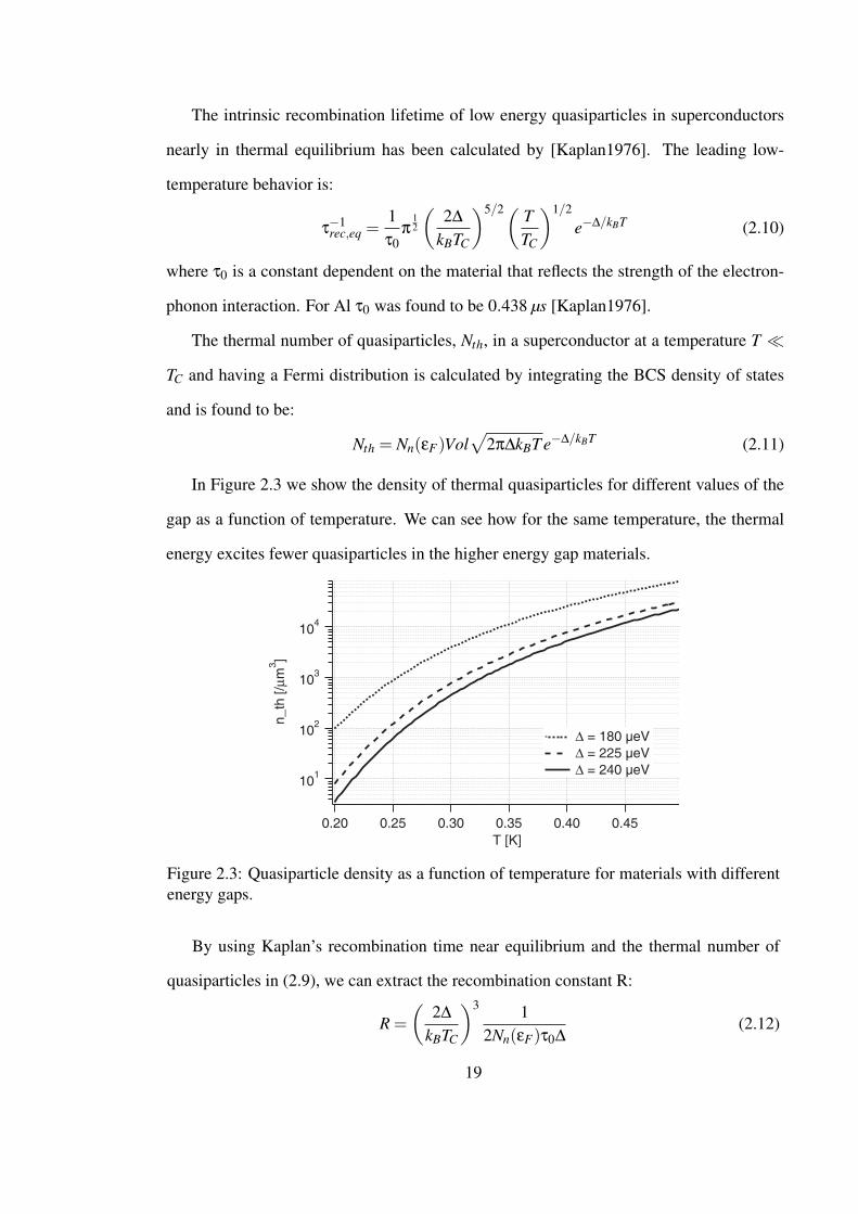
The thermal number of quasiparticles, Nth, in a superconductor at a temperature T ¿TC and having a Fermi distribution is calculated by integrating the BCS density of states
and is found to be:
Nth = Nn(εF)Vol√
2π∆kBT e−∆/kBT (2.11)
In Figure 2.3 we show the density of thermal quasiparticles for different values of the
gap as a function of temperature. We can see how for the same temperature, the thermal
energy excites fewer quasiparticles in the higher energy gap materials.
101
102
103
104
n_
th [
/µm
3]
0.450.400.350.300.250.20
T [K]
∆ = 180 µeV
∆ = 225 µeV
∆ = 240 µeV
Figure 2.3: Quasiparticle density as a function of temperature for materials with differentenergy gaps.
By using Kaplan’s recombination time near equilibrium and the thermal number of
quasiparticles in (2.9), we can extract the recombination constant R:
R =(
2∆kBTC
)3 12Nn(εF)τ0∆
(2.12)
19

For clean aluminum (with ∆ = 180 µeV, TC = 1.2 K), with Nn = 1.5×1047 J−1 m−3 [Kittel]
and τ0 from [Kaplan1976], R has the value of 11.1 µm3/s.
The recombination rate depends on temperature via the thermal background. In Fig-
ure 2.4 the recombination time Γ−1rec when there are no excess quasiparticles is plotted
versus temperature for different values of the energy gap.
10-6
10-5
10-4
10-3
10-2
τre
c [s]
0.80.70.60.50.40.30.2
T [K]
∆ = 180 µV
∆ = 225 µV
∆ = 240 µV
Figure 2.4: Recombination time as a function of temperature for different values of theenergy gap ∆.
After a photon has been absorbed, there are Nexcess excess quasiparticles. By apply-
ing (2.8) and (2.9) to the recombination of excess quasiparticles, we obtain:
∂Nexcess
∂t=−(N2
excess +2NexcessNth)R
Vol(2.13)
The term containing the square of the thermal number of quasiparticles, which is not
shown in (2.13), is cancelled by thermal generation. The first factor in equation (2.13) is
due to the self-recombination of the excess quasiparticles, while the second one is due to
the recombination of the excess quasiparticles with the thermal ones.
We have to remember that during the relaxation in energy of the initially created high-
energy quasiparticles, a hot-spot will be created in the absorber where the effective tem-
perature is much higher than the bath temperature. We should even be careful about de-
20

scribing the system in terms of an effective temperature. In the hot-spot volume the faster
recombination rate would create a loss mechanism for the initial quasiparticles.
Extracting the intrinsic quasiparticle lifetime is complicated in most experiments by
the phonon-trapping effect [Rothwarf1967]. Due to the acoustic mismatch between the
superconducting film and the substrate, a certain fraction of the phonons with energies
larger than 2∆ will be reflected back into the film, continuing to break pairs and to create
excess quasiparticles, thus prolonging the effective recombination lifetime.
2.2 Diffusion Engineering
There are different approaches for achieving intrinsic charge multiplication from the
excess quasiparticles in an STJ, such as gap-engineering and diffusion-engineering. Gap-
engineering involves having the two superconducting electrodes make electrical contact
on each side of the junction to higher-gap superconductors, as in Figure 2.5b. Figure 2.5a
shows the energy band diagram for a gap-engineered device. In this case the charge mul-
tiplication factor depends on the ratio of the two energy gaps, the tunnelling and backtun-
nelling times, the energy relaxation rate in the electrodes, and the quasiparticles’ lifetime.
Diffusion-engineering uses a higher-gap material on only one side of the junction. The
confinement of the quasiparticles on the other side of the junction is controlled by a long
and narrow wire termination, as seen in Figure 2.5d. The energy band diagram in this case
is shown in Figure 2.5c. The wire acts as a constriction that slows down the diffusion of
the excess quasiparticles. If the dwell time around the junction in the counterelectrode is
longer than the backtunnelling time, the quasiparticles will backtunnel, effectively increas-
ing the current in the same direction as the direct tunnelling current. If the quasiparticles
relax in energy before they tunnel, the reverse tunnelling and the reverse backtunnelling
processes are avoided.
21

∆'
∆ ∆
∆'
(a) Gap-engineering energy diagram (b) Gap-engineering top view
∆'
∆∆
(c) Diffusion-engineering energy diagram (d) Diffusion-engineering top viewHigher-gap material
Lower-gap material
Figure 2.5: Energy diagram for devices employing different intrinsic charge multiplicationtechniques. The tunnel junction is between the two lower-gap electrodes.
2.2.1 Diffusion
In our simulations we will only consider a two-dimensional diffusion process. This is
a very good approximation for two reasons:
1. The thickness of our films (0.120 µm) is much smaller than the lateral sizes of our
detector (5×10 µm2 per electrode).
2. The diffusion time over the thickness of each electrode of the junction is much
smaller than the other time scales relevant to our system. For D = 8 cm2/s we obtain a
diffusion time of 18 ps over the 120 nm thickness, while the tunnelling times are on the
order of 5 µs.
The 2D diffusion equation describes the statistical movement of randomly moving
particles in two dimensions. Each particle obeys Brownian motion, as described by a
random walk. The diffusion equation captures the temporal and spatial evolution of the
probability distribution n(x,y,t) of having at time t an average particle density n at point
(x,y). The two-dimensional diffusion equation with no loss is:
22

∇2n− 1D
∂n∂t
= 0 (2.14)
where D is called the diffusion coefficient. Solving this linear partial differential equation
for an infinite plane, in Cartesian coordinates, one obtains:
n(x,y, t) =1
4πDte−(x2 + y2)
4Dt (2.15)
which in polar coordinates is:
n(x,y, t) =1
4πDte−(r2)4Dt (2.16)
This is just a normalized Gaussian function that spreads out in time with a speed that
depends on the diffusion constant.
Figure 2.6: Time evolution of a Gaussian function subject to diffusion and center of massmotion.
Solving the equation becomes more complicated when one introduces boundary con-
ditions and an additional term describing the quasiparticle lifetime. Two types of boundary
conditions describe our system:
1. Dirichlet boundary conditions, specifying the value of the distribution function on a
line, and
23
2. Neumann boundary conditions, specifying the normal derivative of the distribution
function on a line.
2.2.2 Simple Analytical Model
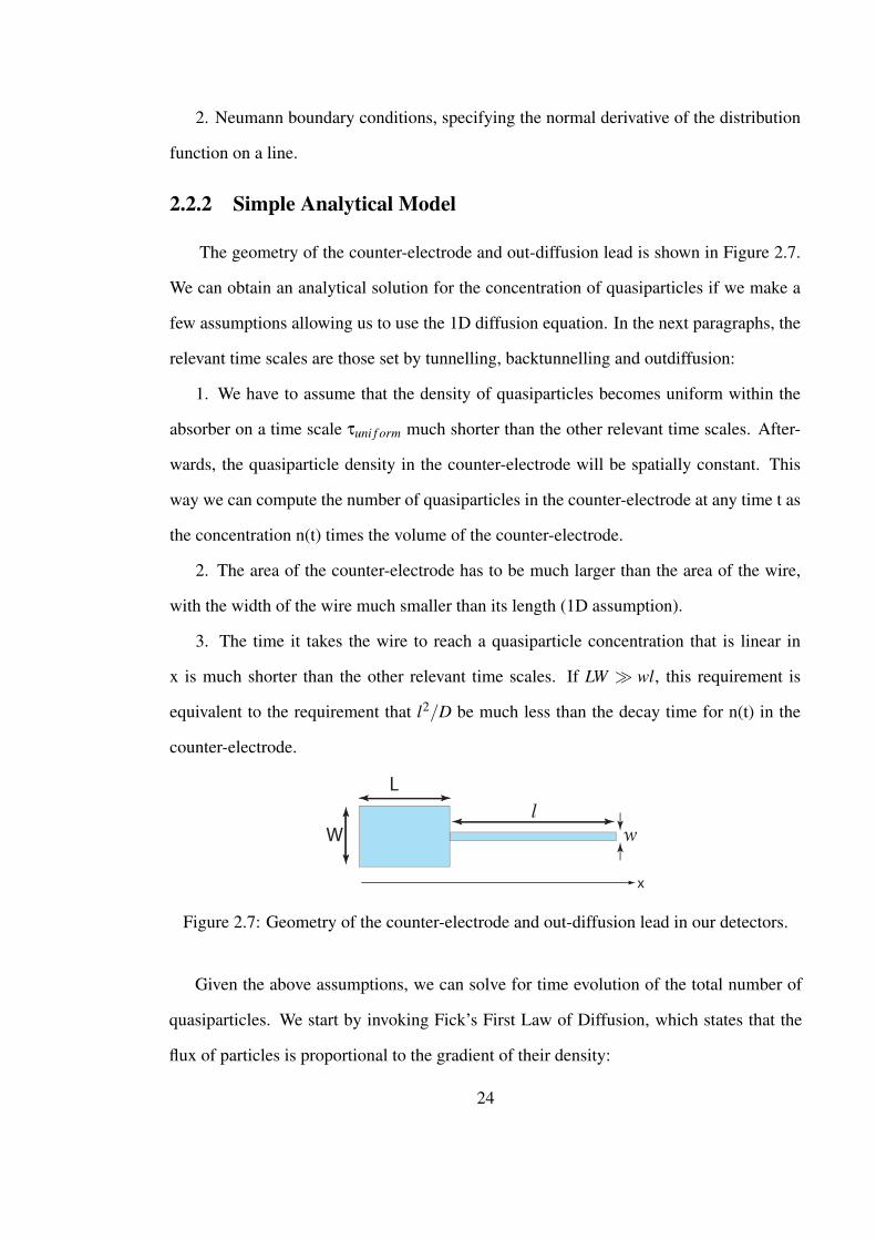
The geometry of the counter-electrode and out-diffusion lead is shown in Figure 2.7.
We can obtain an analytical solution for the concentration of quasiparticles if we make a
few assumptions allowing us to use the 1D diffusion equation. In the next paragraphs, the
relevant time scales are those set by tunnelling, backtunnelling and outdiffusion:
1. We have to assume that the density of quasiparticles becomes uniform within the
absorber on a time scale τuni f orm much shorter than the other relevant time scales. After-
wards, the quasiparticle density in the counter-electrode will be spatially constant. This
way we can compute the number of quasiparticles in the counter-electrode at any time t as
the concentration n(t) times the volume of the counter-electrode.
2. The area of the counter-electrode has to be much larger than the area of the wire,
with the width of the wire much smaller than its length (1D assumption).
3. The time it takes the wire to reach a quasiparticle concentration that is linear in
x is much shorter than the other relevant time scales. If LW À wl, this requirement is
equivalent to the requirement that l2/D be much less than the decay time for n(t) in the
counter-electrode.
L
W
l
w
x
Figure 2.7: Geometry of the counter-electrode and out-diffusion lead in our detectors.
Given the above assumptions, we can solve for time evolution of the total number of
quasiparticles. We start by invoking Fick’s First Law of Diffusion, which states that the
flux of particles is proportional to the gradient of their density:
24

f lux = (−D)dn(x)
dx(2.17)
From the continuity equation, we know that summing up the particle flux flowing out
of the volume gives us the time rate of decrease of the total number of quasiparticles Ntot .
Assuming a uniform flux of quasiparticles along the width w of the lead, we obtain:
f lux×w×d =dNtot
dt(2.18)
By combining (2.17) and (2.18) we can write:
dNtot
dt= (−D)
dn(x)dx
wd (2.19)
In the narrow wire the concentration profile is linear, extending from the spatially con-
stant concentration in the counter-electrode down to zero, at the superconductor / normal
metal interface. From Figure 2.8 we can write down:
n(x+dx)−n(x)dx
=n(L)
l= secθ (2.20a)
dn(x)dx
=n(L)
l(2.20b)
n(x+dx)
n(x)
x x+dxx
lL
n(x)
n(L)
θ
Figure 2.8: Linear quasiparticle concentration profile in the wire.
25

The total number of quasiparticles can be written as Ntot = n(L)×d× (LW + 0.5lw),
due to the linear profile in the lead. Combining (2.20b) and (2.19) we get:
dNtot
dt=− DwNtot
l(LW +0.5lw)(2.21)
The solution to the equation (2.21) has the form Ntot(t) = N0× exp(t/τ), with τ given
by:
τ =1D
lw
(LW +0.5lw) (2.22)
2.2.3 Electrical Equivalent
We can think of the one-dimensional problem in terms of an electrical circuit model.
The counter-electrode acts as a reservoir of quasiparticles, which are discharged through
the out-diffusion lead. Therefore we can model the counter-electrode as a capacitor whose
capacitance is proportional to its total area, CCE ∝ LW . If the tunnelling time is much
shorter than the recombination time in the counter-electrode, CCE = LW . The lead acts as
a two-dimensional resistor where the diffusion coefficient D replaces the conductivity σ.
The three-dimensional formula for resistance R = lσA , with A the transverse area of the
resistor, thus becomes Rlead = lDw . Besides playing the role of a resistor, the lead also
has some associated capacitance, similar to stray capacitance in a circuit. We can think
about the capacitance in terms of the charge (quasiparticles) stored in the lead, yielding
Clead = 0.5lw.
Figure 2.9 shows the RC electrical model. The time constant τ = RC for this circuit
comes out to be equation (2.22). We have not included quasiparticle losses due to quasi-
particle recombination so far in this discussion.
2.2.4 Diffusion Simulation
26

R
C
CCE
lead
lead
Figure 2.9: Electrical circuit model for a diffusion-engineered device.
Although the simple analytical model presented above provides a good first approxi-
mation to be used in our device design, it does not contain the full picture of the diffusion
process. To get a better understanding of the diffusion process, we use Matlab’s Partial
Differential Equation (PDE) Toolbox to solve the parabolic diffusion equation in two di-
mensions:
d∂n∂t−∇(D∇n)+an = f (2.23)
with n being the quasiparticle density. In our case d = 1, D is the diffusion constant, a is a
loss term modelled as τ−1rec, and f is a drive term that is zero.
We use two different types of boundary conditions (b.c.), as seen in Figure 2.10. We
have Neumann boundary conditions on all sides except the end side of the wire. The
Neumann b.c. sets the normal component of the quasiparticle flux. In our case this is zero
since the quasiparticles cannot leave the boundaries except through the end of the wire. At
the end of the wire there is contact to a normal metal or a very large area superconductor,
where there are no excess quasiparticles. For this boundary we have Dirichlet type b.c.,
setting the distribution function to zero.
∆
n=0.
n=0
Figure 2.10: Dirichlet and Neumann boundary conditions set on our domain.
27

No other loss mechanism is taken into account in our simulation. The two-dimensionality
of our problem is valid as long as the thickness of our layers is much smaller than the small-
est geometrical feature in our design, the wire width. In practice, the total layer thickness
is 0.12 µm, while the wires are as narrow as 0.25 µm. We can still use the results with the
caveat that the quasiparticles will take shorter than the simulated time to out-diffuse down
the wire. Effectively, the third dimension (thickness) can be folded into a larger second
dimension (width).
The input simulation parameters are:
• the diffusion constant D [cm2/s],
• the electrode and wire dimensions W, L, w, l [µm],
• the quasiparticle initial spike position and the total number of quasiparticles in the
spike,
• the loss time,
• the time range for which the simulation should be run [µs] and the time resolution
[ns/frame], and
• the percentage of quasiparticles left.
We monitor three regimes, recording the time at which each starts. In chronological
order, we have:
• uniformity - the time after which the density of quasiparticles reaches uniformity in
the electrode,
• linearity - the time after which the quasiparticle density profile becomes linear in the
lead (this is also the steady state solution for our system),
• percentage reached - the time after which the desired percentage of quasiparticles is
left in our system.
After the system reaches linearity, the total number of quasiparticles in the system at
each point in time can be calculated easily. Since in the electrode the concentration is
spatially constant n(L) and in the wire it is linear from its value in the electrode down to
28

0
20
40
60
80
0
1
2
3
4
5
0
10
20
30
40
50
60
70
80
n(x,y)
xy
(a) Quasiparticle concentration in the counter-electrode becomes uniform.
0
10
20
30
40
50
60
70
0
1
2
3
4
5
0
10
20
30
40
50
60
70
n(x,y)
yx
(b) Quasiparticle concentration in the lead be-comes linear.
0
10
20
30
40
50
60
70
0
1
2
3
4
5
0
10
20
30
40
50
60
70
n(x,y)
y x
(c) 33% of quasiparticles have diffused out thelead
Figure 2.11: Evolution in time of the quasiparticle concentration in the counter-electrodeand lead. The initial number of excess quasiparticles is 4000, the electrode area is 5×10 µm2, and that of the wire is 0.25×62 µm2.
zero, the total number is Ntot = n(L)× (LW + 0.5lw). This is the regime for which our
simple 1D model was valid, but now we have the 2D version of it.
The simulations have been done with the same initial number of 4000 quasiparticles
and a time resolution of 100 ns unless otherwise stated.
Uniformity
With a diffusion constant of 8 cm2/s, it takes under 10 ns for the initial hot spot of
quasiparticles to spread out uniformly within the 5×10 µm2 area of our electrode. For as
slow a diffusion as 2 cm2/s, an area of 5× 10 µm2 becomes uniformly filled in less than
200 ns. So for any practical cases , the uniformity time scale is very short compared to the
microsecond timescales of the other relevant processes.
29

Linearity
The time τlinear simulation to reach the linear regime in the lead depends on many pa-
rameters. In Figure 2.12 we show the variation with the diffusion constant. As expected,
this time increases as the quasiparticles diffuse more slowly. We can vary the value of the
Al diffusion constant from 1− 60cm2/s, depending on the impurity concentration incor-
porated in the film.
4
3
2
1
τlin
ea
r_sim
ula
tio
n [
µs]
605040302010
D [cm2/s]
CE: 5 X 10 µm2
Wire: 0.25 X 62 µm2
Figure 2.12: Variation of the time for the concentration profile in the wire to become linearwith diffusion constant.
Out−diffusion
In Figure 2.13 we compare the time obtained from the simulation to the time obtained
from using the linear regime formula. The simulation time was computed as the time after
which 36% of the initial number of quasiparticles are left in the electrode and wire. As
input parameters we used diffusion constants from 2 cm2/s up to 60 cm2/s, a counter-
electrode of 5×10 µm2, a lead of 0.25×62 µm2, and a loss time of 150 µs.
We notice the deviation from the linear regime formula as the out-diffusion time gets
longer. The linear regime formula τout f ormula overestimates the out-diffusion time ob-
tained from the simulation, τout simulation. This effect becomes more relevant for the slower
diffusion cases, i.e. for the smaller diffusion coefficients, reaching a discrepancy of about
30%. This is due to quasiparticle recombination losses, which become more significant at
longer times.
30

70
60
50
40
30
20
10
τou
t_sim
ula
tio
n [
µs]
70605040302010
τout_formula [µs]
Data
Fit
Figure 2.13: Fit with a slope of 1 for times up to 20 µs of the simulation time versus thetime calculated with the linear regime analytical formula.
2.3 Diffusion Engineering Flowchart
In this section we examine the constraints we encounter in designing the diffusion-
engineered devices and the relation between different parameters. This is presented schemat-
ically in Figure 2.14. We will investigate each parameter on the last rows of the chart and
see how we can solve some of the associated conflicting requirements.
Our aim is to maximize the signal-to-noise ratio, S/N, in our detector. The signal is the
collected charge, which is proportional to the charge multiplication factor p and the initial
excess number of quasiparticles N0 created by the absorbed photon. N0 is a function of the
energy gap of the absorber and the photon energy. The charge multiplication factor is the
ratio of the out-diffusion time to the tunnelling time. In a single-tunnelling device p = 1,
while in a diffusion-engineered device we want to be able to maximize p. The flowchart
in Figure 2.14 has dashed lines going to the parameters that need to be minimized, and
continuous lines going to the parameters that need to be maximized. We notice how some
parameters need to follow opposite directions (be at the same time minimized and maxi-
mized) dictated by optimization of different parameters. For these cases an optimum value
has to be achieved. In certain situations the direction of change for some parameters will
not be the one indicated in the chart due to other constraints. I will explain each case.
31

p = τout
τtunn
τtunn
~ R Vol E - 2 l 1
w D τ = (LW+0.5lw)
out
R n
n
Vol D L W w l
d Aj W Lox d
Wd r1
2
i n ~ e
R
1 - / k T
T n
Rn
2
S/N
minimize
maximize
B
Figure 2.14: Diffusion engineering flowchart reflecting the different connections betweendevice parameters.
Lowering the intrinsic device noise contribution also increases the signal-to-noise ratio
of our measurements. The device intrinsic current noise is in ∼√
Idc. From equation (2.5)
we see that both a lower working temperature and a higher normal resistance would have
the desired effect. The higher normal resistance is achieved by making the junction area A j
smaller and by lowering the junction current density jC; jC is proportional to the junction’s
conductance and depends on the oxide barrier thickness dox. In practice there is a limit to
the oxidation achievable without introducing an unacceptable amount of impurities. The
lower limit is set by how uniformly one can achieve the thinnest oxide layer. In practice,
for the Al junctions fabricated in our facilities, the critical current density jC of the junction
is limited to a range of 10−175 A/cm2. If we want even smaller device current noise, we
need to fabricate smaller junctions.
Previously we used an optical lithography tri-layer junction process followed by wet
etch patterning, which limited our junction sizes to tens of squared microns, with no size
32
smaller than 7 µm. In practice, the lowest subgap current at 0.24 K was on the order of
1.5 nA. By switching to the Dolan bridge double-angle fabrication technique (as explained
later in the fabrication chapter) we were able to fabricate junctions as small as 1×5 µm2.
These smaller junctions have a much smaller current noise than larger junctions, if op-
erated at the same temperature. Although smaller-size junctions would have even less
current noise, their tunnel time would be much longer, possibly longer than the loss time
in the device. One way to decrease the tunnel time while keeping the junction size small is
to make the junction more transparent, i.e. with a higher jC. However, high-transparency
oxide barriers tend to develop superconducting shorts, where the non-uniformity of the
oxide allows the two electrode layers to touch. This translates into a critical current that
cannot be suppressed, making voltage-biasing the junction difficult and increasing the sub-
gap current of the device. All our designs have 1×5 µm2 junctions. This allows us to go
to a sub-gap current as low as 0.1 to 0.2 nA, a factor of 10 better than with the previous
tri-layer process.
The tunnelling time has to be longer than both the quasiparticle energy relaxation time
and the fastest time we can detect, which is set by our electronics bandwidth, and is on
the order of a couple of microseconds. If we want a large charge multiplication factor,
the diffusion time should be longer, limiting the detector’s speed. So we decided that the
mid-ground between these two conditions is a tunnel time of 5 µs.
With the tunnelling time decided from the above considerations and the maximum
junction area set by the nature of the fabrication process, we had to adjust the oxidation
time accordingly.
While for minimizing the tunnelling time we would want small electrode dimensions
L and W, for maximizing the out-diffusion time these have to be made large. So we have
to optimize the geometry using these constraints.
The width of the out-diffusion lead, w, has to be small. Its size is determined by
how narrow we can reproducibly fabricate a uniform and long line. Non-uniformities can
33

influence the local energy gap value, possibly introducing undesired trap-centers in regions
with lower gap. At the same time, the out-diffusion lead should be as long as possible.
The energy gap ∆ can be increased by using a higher-gap material, achieved by using
‘dirty’ aluminum. We decided to continue using Al for our junctions, given the high
yield and reliability of the fabrication process. What we refer to as ‘dirty’ aluminum is
aluminum with an enhanced energy gap, achieved by deposition in an oxygen background.
The ‘dirtier’ the aluminum, the higher the gap, meaning smaller grains that slow down the
quasiparticle diffusion. So having higher gap aluminum was a requirement consistent with
having a smaller diffusion constant D.
34

Chapter 3
Experimental Setup
3.1 Overview
In this chapter we present the setup used for our experiments. Much of the experimental
apparatus was constructed by previous researchers at Yale, and it is described in detail
in previous theses [Gaidis1994], [Friedrich1997], [Segall2000], [Li2002], [Wilson2002].
We shall emphasize those aspects that are new or modified. The experimental setup is
schematically presented in Figure 3.1. The devices are mounted inside a cryostat with the
base temperature of 0.24 K. A custom-made battery-powered electronics box is used to dc-
bias the junction in the sub-gap region and to amplify the ac-current signal from the device.
The cryostat and the electronics box are located in a bigger shielding box, which prevents
electromagnetic interference. The pumping lines for the cryostat fit through a hole into
the shielding box. The ac signal is further amplified and filtered outside of the shielding
box before it is recorded on an oscilloscope. The data are downloaded via GPIB1 to a
computer, where they are later analyzed. The optical testing is done using an attenuated
beam from an ultra-violet pulsed laser. The light is coupled from the laser to the device via
optical fibers. An optically-synchronized electrical signal from the laser is used to trigger
the data recording.
1General Purpose Interface Bus is an interface system that connects programmable instruments to theircomputers
35
Figure 3.1: Experimental setup.
3.2 Cryogenics
For testing our devices at cryogenic temperatures we use a custom-made, two-stage, pumped
3He dewar, known as Tiny Tim. It has a liquid N2 stage, a liquid 4He stage and two closed-
cycle 3He pots. The stages are nested into each other, and all the pumping lines and con-
tacts for the second 3He pot are pre-cooled through the first one. Inside the 4He stage there
are two charcoal absorption pumps for the two pots. The copper cold finger is connected
to the second pot, allowing the base temperature to reach 0.24 K.
We start the cool-down procedure by pumping out the dewar with a turbo pump, out-
side the shielding box. We wait for the pressure to drop down to 10−4 Torr, which takes
about 7 hours. While still pumping, we pre-cool both the N2 and the 4He tanks with liquid
N2. It takes a minimum of 3 hours for the temperature to come down to 77 K, but we usu-
ally leave the liquid N2 in overnight. We remove the liquid nitrogen from the helium tank
with pressurized helium gas, making sure no liquid is left in the tank. We stop pumping
36

on the dewar just before transferring liquid 4He into the 4He tank. The 4He stage reaches
4 K in about half an hour, after which we top it off with more helium. The dewar is then
transferred into the shielding box and we start pumping on the liquid 4He. In about 20
minutes the base temperature reaches 1.5 K, which is low enough to start condensing the
3He. We open valves from the pressurized room temperature 3He cylinder attached to the
side of the dewar, allowing the 3He to condense into the two pots. Full condensation is
attained in one hour. The condensed 3He pots are thermally disconnected from the 4He
stage and the charcoal absorption pumps are instead thermally connected to it. The cold
charcoal starts absorbing the vapors on top of the condensed 3He, lowering the pressure
and therefore its temperature. The base temperature is reached in about 2 hours and lasts
for the next 6 hours. The first stage is cooled to about 0.3 K. The second stage is cooled
to 0.24 K through a pumping line cooled through the first stage.
Half an hour before taking data we start pumping with a turbo pump on the liquid N2
tank. Lowering the temperature makes the nitrogen slushy, preventing it from ‘bubbling’.
Without this precaution, there were mechanical vibrations from the nitrogen bubbles which
used to be picked up as electrical noise by the wiring leading to our samples. Freezing the
nitrogen in this fashion solved the problem.
At the end of the experiment we stop pumping on both the nitrogen and the helium, we
thermally reconnect the 3He pots to the 4He bath, and we open the valves that allow the
3He to evaporate into the 3He room temperature cylinder. To prevent water condensation
inside the cryostat, we do not open the dewar for at least 12 hours.
3.3 Electronics
3.3.1 Electrical Contacts
In early experiments the contact from the device’s contact pads to the 0.2 K stage wires
was done using Pogo pins from Emulation Technology, Inc. After 08/18/2004, we decided
to change the contact technique for two reasons: first, the new devices are fabricated using
37

only e-beam lithography, so macroscopic 1×5 mm contact pads for the pogo pins would
take a long time to pattern; second, the pogo pins had a limited and relatively short lifetime
if thermally-cycled many times, the main failure mode being becoming open only at low
temperatures. The new contact technique uses wire-bonding. The bonding is easily done
with Al wire from patterned 150× 400 µm Au pads onto 0.75 cm wide Cu traces. The
traces, deposited on top of a circuit board piece, connect to a 20-wire ribbon cable. Since
the cryostat has only 12 wires available, the 8 unused wires from the ribbon cable were
cut short and left unconnected. The chip with the device is glued down with GE varnish2
to a Cu pad located roughly in the middle of the circuit board piece. The Cu pad insures
a better thermal contact to the 0.2 K cold finger. The circuit board piece is placed in good
thermal contact with the cold finger via a thin layer of Apiezon N thermal grease.
circuit board with Cu traces
quasi-Helmholtz coils
chip with devices
Figure 3.2: Circuit board with Cu traces and wire-bonded devices on a chip, along withthe quasi-Helmzoltz coils used to produce a parallel magnetic field.
2GE varnish 7031 is an adhesive and electrical insulator, usually used when good thermal contact isdesired.
38

3.3.2 DC Electronics
The 12 wires are tightly wrapped around the several cold stages before being connected
via a hermetic military connector outside the dewar to an electronics box. The electronics
box supports two dc lines, for monitoring the devices’ dc bias point (voltage and current),
and one ac line, for recording the device’s ac current response. The dc-bias circuitry and
the first stage of the ac amplification chain are located on a printed circuit board (PCB), in
a 18×12×8 cm3 metal box. In order to minimize the 60 Hz interference from the power
lines, the amplifiers and voltage regulators on the PCB are powered solely by 9 V and 6
V batteries, located inside the same box. The box has two BNC coaxial outputs for the
dc lines and one triaxial output that carries the ac signal. The schematic of the electrical
circuit in the box is shown in figure 3.3.
Due to the non-linear I(V) characteristics of a tunnel junction, we have to choose care-
fully the dc biasing scheme for the device. If the load line of our biasing circuit intersects
the I(V) characteristic of the device more than once, the biasing can be unstable and in-
troduce noise in our measurements. When the critical current is not suppressed, we would
need a load line stiffer than 50Ω to be able to voltage bias at 100 µV without intersecting
the critical current branch, on the order of 2 µA for our devices. To avoid this problem,
we start the experiment by current biasing our device, switching to voltage bias once the
critical current is suppressed below 50 nA.
After cooldown we first current-bias the junction through a 2 kΩ resistor. The critical
current of a tunnel junction has a periodic behavior with the applied parallel magnetic
field. Every time the flux Φ penetrating the junction is an integer of the flux quantum
Φ0 = 2.07×10⁻¹⁵ Wb, the zero-voltage current averages out to zero. We next adjust the
magnetic field to correspond to one of the zeroes in the critical current. Usually the best
suppression is achieved at the third zero, which requires a magnetic field of about 60 G.
Once the critical current is suppressed by a factor of 10−2, below 100 nA, we change to
a more sensitive current scale by switching out the 2 kΩ resistor and connecting a 1 MΩ
39
resistor. We then suppress the critical current down to about 10 nA.
Given the good suppression of the critical current, we adjust the current-bias to zero
and then switch to voltage-bias. We fine-tune the external parallel magnetic field for op-
timum critical current suppression. For voltage-biasing we use a loop in parallel with the
input of a low-noise, large-bandwidth Amptek A250 amplifier, whose input needs to be
kept at 3 V. The loop consists of two amplifiers: an OP97 that monitors the voltage across
the device, and an OP77 voltage comparator. The OP77 compares the device voltage to
a reference voltage and compensates the source-drain current of a FET connected at the
input of the A250. This keeps the input voltage of the A250 at 3V. The junction is voltage-
biased in the flattest region on the subgap I(V) curve, around 110 µV.
For both biasing schemes, the dc voltage is measured directly across the sample by
an INA110 amplifier with a gain of 500. When current-biasing, the device dc current
is inferred by measuring the voltage across the bias resistor. When voltage-biasing, the
device dc current is inferred from the A250 output voltage. In both cases, the measured
voltage is amplified with unity gain using an INA110 amplifier. Both dc signals go into
ISO100 optical isolation amplifiers. These amplifiers prevent noise from coupling back to
the device.
Outside the electronics box, the dc lines are sent through BNC cables outside of the
shielding box. At the exit from the shielding box, the signals are filtered using custom-
made T-filters [Wilson2002].
3.3.3 AC Electronics
The ac signal is amplified using the same A250 used for voltage-biasing, now in a trans-
impedance configuration. The A250 is coupled to the device through a discrete input
FET [Friedrich1997], making it a very good composite amplifier. The transistor that best
matches our detector characteristics is the Toshiba 2SK146 FET. The composite amplifier
draws current from the device on the feedback resistor, converting the input current into
40
an output voltage. The gain is set by the feedback resistor, which is 1 MΩ. The feedback
resistor is anchored at the 1.5 K stage so that its Johnson current noise SI =√
4kBT/R is
reduced to 9 fA/√
Hz. The signal is further amplified by a factor of 10 with an INA110
amplifier.
The ac signal outside of the shielding box is carried by a short triaxial cable to a
12× 9× 6 cm3 box. There it is amplified by a factor of 10 using an INA110 amplifier.
Amplifying the signal at this stage decreases the effect of pickup noise along the cables
outside the shielding box. This box output feeds into a Princeton Applied Research (PAR)
113 amplifier, which is battery-powered during the experiment. The PAR is usually set
to have a gain of 10 and to band-pass filter the signal in the 0.3− 100 kHz range. The
lower frequency limit eliminates the 1/f noise. The higher frequency limit is on the or-
der of the signal frequency and well within the A250 300 kHz bandwidth. This rejects
higher frequency noise. The PAR output goes into the digital oscilloscope, where data are
recorded.
3.3.4 Magnetic Field
In order to accurately measure the quasiparticle subgap current, we have to suppress the
Cooper pair current. This is done by applying a magnetic field parallel to the junction
plane. The magnetic field required for critical current suppression is produced by a pair
of quasi-Helmholtz3 superconducting coils made of NbTi wire. The field is adjusted
by changing the current flowing through the coils, which is provided by a custom-built,
battery-powered, high-current source located in a metal box inside the shielding box. The
circuit board with the device is located in the center of the two coils, where the field is
uniform and maximum.3Helmholtz coils are a pair of circular coils on a common axis with equal currents flowing in the same
sense. For a given coil radius, the separation needed to give the most uniform central field is equal to theradius of the coils. Our quasi-Helmholtz coils are separated by 7.75 cm, larger than the coils’ 4.5 cm radiusto allow a larger usable area on the cold finger.
41

Figure 3.3: Active voltage biasing electronics, with the cross indicating our device.
3.4 Shielding
The experiments take place in a shielding box made by Lindgren RF-Enclosures, Inc..
The box is 1.6×1.6×1.6 m3, with 5 cm thick walls, providing electromagnetic shielding
from 150 kHz to 10 GHz. Each 5 cm thick wall is made by 6 mm steel plates separated
by plywood. The dewar is 64 cm tall and has a 36 cm outer diameter. A 3 mm thick
mu-metal cylindrical shield, 50 cm tall and 47 cm in diameter, surrounds the lower half of
the cryostat, where the cold finger is located. The mu-metal shield screens the static and
low-frequency magnetic fields that would otherwise interfere with the device.
42
3.5 Optics
A detailed description of our optical setup can be found in [Wilson2002]. We test our
devices with photons coming from either a Hg lamp which emits at different wavelengths,
or from an ultraviolet (UV) pulsed VSL-337ND-S nitrogen laser, manufactured by Laser
Science, Inc., whose output is at 337 nm. The light is guided through an optical fiber
from either source to an optical bench. There it is filtered: we use color filters for single
wavelength selection of the light coming from the lamp and neutral density filters for
adjusting the intensity once we have monochromatic light. After the filters the light is
collected into another optical fiber which feeds into the shielding box. From there another
fiber is connected to a vacuum-tight feedthrough which goes into the dewar. Inside the
dewar we have an Al-coated fiber, that wraps around the different cold stages. The fused
silica fiber has a high OH content, the impurities absorbing the infrared radiation from
room temperature and different cold stages. Thus we effectively filter the black-body
radiation coming down the fiber from the cold stages. All fibers are terminated with SMA
connectors except the fiber end that is aligned to the sample. We use multimode fibers
that have a core diameter of 300 µm, a numerical aperture N.A.= 0.22, and operate at
wavelengths between 250−800 nm. The fiber is manually aligned to the devices. Usually
it is located 1 mm away from the substrate. The light cone spreads over an area of 0.5
mm2 on the substrate, four orders of magnitude larger than our device area. Using a
singlemode fiber (with a much smaller core diameter) would decrease the area over which
the photons are spread, but would make the light coupling into the fiber more difficult.
We tried focusing the light onto the device, but the smallest spread area was still large,
0.03 µm2.
The maximum internal pulse repetition rate of the laser is 30 Hz and the pulse width
(FWHM) is less than 4 ns. The ‘OptoSync’ laser output provides an optically-derived TTL
signal to allow synchronization of the external experiment with individual laser pulses. It
has a very low temporal jitter relative to the laser pulse (< 1 ns), so we use it as a trigger
43

signal in our data acquisition system. The laser wavelength of 337 nm corresponds to an
energy of 3.68 eV.
3.6 Data Acquisition
We use a 20 MHz digital oscilloscope, Nicolet Integra 40, for recording the pulses and
noise traces. When the laser is used to test our devices, we use the TTL laser output
signal ‘OptoSync’ as a trigger signal for recording the pulses. When the Hg lamp is our
light source, the trigger level is set manually. Different data sets are acquired for different
trigger levels. The levels are set around the value for which a significant change in the
pulse detection rate is noticed.
Each pulse is digitized into 2000 points, with the first 500 points being the pre-trigger
signal. Every 100 pulses the oscilloscope sends the data via a GPIB cable to the computer.
A set of data is called a ‘run’ and it usually contains 4000 pulses. More pulses would
provide better statistics, but the acquisition time for 4000 pulses is 20 minutes. The ex-
perimental time of 6 hours at the base temperature sets a hard limit on the time we have to
allocate for exploring the large parameter space (such as different voltage biases and dif-
ferent light intensities) of our different device generations. Taking relevant data for at least
a single-tunnel and a diffusion-engineered device during one cool down was paramount
for extracting information that would determine our next generation designs. For noise
measurements, we acquire long noise traces that are sent to the computer, where they are
fast Fourier transformed. Typically 100 resulting noise spectra are averaged and the aver-
aged spectrum is saved. The data are analyzed using existing and user-created procedures
in IgorPro, a scientific graphing and data analysis software developed by WaveMetrics.
We use the average pulse shape to optimally filter the pulses (the power spectrum of the
noise is approximately constant in our measurement bandwidth). We obtain the charge by
digitally integrating the current pulses.
44

Chapter 4
Fabrication
4.1 Overview
Our devices are fabricated using several steps of lithography. The chronological order of
the steps involved is:
• Wafer oxidation
• Ta deposition on the whole wafer
• Resist spin and pattern - Ta ion-milling of individual chips
• Resist spin and pattern - Au deposition
• Resist spin and pattern - Al deposition
In this section I will explain the process of Si wafer oxidation, present the general
principle of e-beam patterning, and introduce the microfabrication machines used. In the
following sections, each fabrication step will be discussed individually in detail.
As device carriers we use 300 µm thick, 2” in diameter oxidized silicon wafers. Oxida-
tion of Si refers to the process of growing a layer of silicon dioxide on the wafer surface.
The silicon dioxide layer acts as an insulator between the different metallic structures to
be fabricated and the substrate. The wafers are placed in a furnace for 60 minutes at a
temperature of 1000 C. We use wet oxidation, which involves having a stream of water
45

vapors flowing across the wafers while in the furnace. We measure an oxide thickness of
225 nm using an interferometer.
The lithography is done with the field-emission high-resolution scanning electron mi-
croscope(SEM) FEI XL30 Sirion which has been converted into an electron beam (e-
beam) writing system. We pattern the resist with an e-beam accelerated by 30 kV and
having the sample at a working distance of 10 mm from the e-beam gun. For viewing
the samples we use a 10 keV e-beam at a working distance of 5 mm. Using e-beam is
necessary for gaining access to all sub-micron features, providing also a dynamic platform
for design changes.
In transferring the desired patterns onto the oxidized wafer we use chemical substances
sensitive to electrons, known as e-beam resists. For each metal layer step, we spin resist on
a spinner located in a class 1000 cleanroom. The resist thickness is set by the resist type,
the speed of the spinner vacuum chuck (usually several thousand rpm) and the spinning
time (usually 60 seconds); for a thinner resist layer, we want a lower-viscosity resist spun
fast and for a long time. After spin coating the wafer, we write our pattern with the e-beam
into the resist. There are two types of e-beam resists: positive and negative. For positive
resists, the resist is exposed with a beam of electrons wherever we want it to be removed.
In these resists, exposure to the e-beam changes the chemical structure of the resist so
that it becomes more soluble in the developer. The exposed resist is then washed away by
the developer solution, leaving windows of the bare underlying material. Negative resists
behave the opposite way, the developing solution removing only the unexposed areas. For
all our processes, we use positive resists. The sample is developed for 48 seconds in a
mixture of 1:3 methyl isobutyl ketone (MIBK) and isopropanol (IPA). The MIBK is the
active solvent, while the IPA dilutes the MIBK, thus controlling the developing speed. The
developing process is stopped by immersing the sample for 10 seconds in IPA. Nitrogen
gas is used for blow-drying the sample.
46

For each patterning step we use different resist types and different process parame-
ters. We use PMMA (polymethyl methacrylate) positive resist in anisole and MMA-MAA
(copolymer) resist in ethyl lactate from MicroChem Corp. All the PMMA resist types
used in our processes have a 950,000 molecular weight and come in different concentra-
tions in the anisole solvent. For example, 950PMMA A6 has 6% PMMA in anisole sol-
vent. The copolymer is a mixture of PMMA and methacrylic acid in ethyl lactate solvent.
MMA(8.5)MAA EL13 has 13% PMMA with 8.5% methacrylic acid in ethyl lactate. The
copolymer offers a higher sensitivity to e-beam than PMMA, with a tradeoff in contrast.
It is used as a bottom layer in bi-layers with PMMA, to produce undercut profiles.
The metal layers are deposited in the high-vacuum (HV) Lesker Sputtering System and
in the Plassys electron beam evaporator system. The techniques used are dc-sputtering
and thermal evaporation in the Lesker, and electron-beam evaporation in the Plassys. The
Lesker system has a 3 cm Kaufman argon ion gun used for milling Ta and for ion-beam
cleaning the samples before metal depositions. The Plassys system has an Anatech ion
gun used for cleaning the samples before metal deposition steps.
After metal deposition on a patterned substrate, the resist with metal on top is removed
using the lift-off technique. The sample is soaked in 75 C acetone for at least 20 minutes,
followed by 1 minute of ultrasonic agitation. The metal on top of the resist lifts off as the
resists dissolves in the acetone. The sample is rinsed with methanol before the acetone
evaporates. The methanol is blow-dried with dry nitrogen gas.
For all the measured samples the Ta has been deposited in the Lesker system and the
Au in the Plassys. The Al on Chip1 was deposited in the Lesker via thermal evaporation,
while for Chip2 and Chip3 were deposited in the Plassys e-beam evaporator. In the next
sections I will describe in chronological order the device fabrication steps on the oxidized
wafer.
47
4.2 Ta Deposition
We start by dc-sputtering tantalum in a Lesker thermal evaporator/dc-sputtering system.
We let the wafer bake at 350 C for 12 hours in the vacuum chamber until the pressure
goes down to 2×10⁻⁸ Torr. We then clean it with an ion-beam for 2 minutes just before
the deposition. The Ta is heated up to at 750 C and then sputtered at a rate of 10 nm/s
over the whole wafer. We let the wafer cool for 3 hours without breaking vacuum. All the
measured samples were fabricated using the same 70 nm Ta wafer.
4.3 Ta Ion-Milling
We spin a 2500 nm double layer of MMA(8.5)MAA EL15/950PMMA A8 (positive re-
sists) on the whole wafer covered with sputtered Ta. The parameters for the resist process
are listed in table 4.1. We then cut the wafer into several chips using a diamond tip scriber
and continue the next steps on each individual chip. The writing ‘unit cell’ consists of 4
devices that will share the same Ta alignment marks. Each set of 4 devices covers a chip
area of about 4×6 mm2. The e-beam patterning is done such that there is no resist where
we want the Ta to be removed.
We use the Lesker ion-gun to ion-mill the Ta which is not covered by resist. The
ion-beam current is 4.7 mA and the beam voltage 500 V. Etching away 70 nm Ta takes
about 9 minutes. The thick double resist layer is used to protect the Ta under it during the
milling process. The left-over resist is removed in an ultra-sound bath while soaking in
hot acetone. The only features on the chip are now one Ta plug per device and a set of 4
alignment marks for each set of 4 devices.
4.4 Au Deposition
Gold electrodes form the second layer. We spin 950 PMMA A6 at 2000 rpm for 1 min
and bake it at 170 C for 30 min. The resist thickness is 600 nm. We pattern it such that
48

Resist MMA(8.5)MAA EL15 950 PMMA A8Spinning speed [rpm] 1500 3500Spinning time [min] 1 1Baking temperature [C] 170 170Baking Time [min] 1 25Cooling time [min] 1 1Resist thickness [nm] 1750 750
Table 4.1: Resist process parameters for Ta
the regions we want Au deposited on are not covered by resist. We use the Ta alignment
marks to align our e-beam writing to the previous existing structures.
The parameters used for the Au deposition are summarized in Table 4.2. We first clean
the sample with an ion beam for 2 minutes. A thin 3 nm layer of Ti is first deposited at a
0.2 nm/s rate. It is used to enhance the Au adhesion to the SiO2 surface. The 100 nm thick
Au layer is deposited at a 0.5 nm/s rate. This is a thickness for which the wire-bonding to
the Au pads quality is consistently good.
Pressure [Torr] Before Chip1 and Chip2 [Chamber/Load Lock] Chip3 [Chamber/Load Lock]Ion Beam Cleaning 1.7×10⁻⁷ / 1.7×10⁻⁶ 1.0×10⁻⁷ / 6.5×10⁻⁷
Ti Deposition 1.8×10⁻⁷ / 1.1×10⁻⁶ 7.6×10⁻⁸ / 4.9×10⁻⁷
Au Deposition 3.1×10⁻⁸ / 3.3×10⁻⁷ 8.0×10⁻⁹ / 2.0×10⁻⁷
Table 4.2: Parameters for Au deposition in the Plassys.
4.5 Junction Fabrication
The tunnel junctions are fabricated using the Dolan-bridge technique [Dolan1977]. A
double-layer of MMA/PMMA resist is spun on the chip, with the parameters found in
Table 4.3.
Two openings which later will become the junction electrodes are patterned 1 µm apart
in the resist. Due to the faster solubility of the exposed copolymer than that of the exposed
PMMA in the developer, we create an undercut in the lower resist layer. The space be-
49

Resist MMA(8.5)MAA EL15 950 PMMA A6Spinning speed [rpm] 2000 2000Spinning time [min] 1 1Baking temperature [ C] 170 170Baking Time [min] 1 30Cooling time [min] 1 1Resist thickness [nm] 1450 550
Table 4.3: Resist process parameters for Al junctions.
tween openings being comparable to the undercut size, a hanging resist bridge (made of
the second resist layer) is created after the developing process. Figure 4.2 sketches this
technique.
(a) Start with a double layer of resist (b) Expose 2 rectangles which are apart a dis-tance on the order of the undercut.
(c) Develop the resist and obtain a resistbridge from the second resist layer.
Figure 4.1: The Dolan-bridge patterning technique [not to scale].
Before the Al deposition, the sample is ion-beam cleaned for 2 minutes. The first Al
layer has an effective thickness of 50 nm and is deposited at an angle of 40 from the
normal to the sample. We let the sample cool down for 2 minutes and then oxidize it to
form the junction. By varying the amount of time and the dry O2 pressure during oxidation
we can change the junction transparency, i.e. the super-current density. We then pump out
the O2 and deposit the second layer of 70 nm Al perpendicular to the sample.
50

(a) Resist bridge over the substrate
1st Al layer
(b) First layer deposition at an angle.
2nd Al layer
(c) Second layer deposition perpendicular tothe sample.
Spurious big junction
Spurious big junction
Desired junction
(d) Resist ready for lift-off
Figure 4.2: Cross-sectional view of the Dolan-bridge double-angle evaporation technique[not to scale].
The Al on Chip1 is deposited in the Lesker. The system is pumped down to 3×10⁻⁸
Torr before the ion-beam cleaning. The junction is formed by oxidation at 1 Torr for 20
minutes. We then pump out the oxygen, reaching a 2×10⁻⁶ Torr pressure and deposit the
second Al layer. The Al deposition rate was for both electrodes 0.3 nm/s.
The Al on Chip2 and Chip3 is deposited in the Plassys. We begin by evaporating
titanium at a rate of 0.1 nm/s for 50 seconds with the shutter covering our sample. The
Ti deposition helps to lower the pressure in the vacuum chamber, without being deposited
on our samples. The aluminum is deposited at a 1 nm/s rate for both electrodes. The
oxidation is done in a mixture of Ar/O2, with 15% partial pressure of O2 in Ar. Table 4.4
has the process parameters.
The Al in the three samples has been deposited in the presence of different oxygen
levels. This affects the purity of the Al, changing its superconducting energy gap and
its diffusion constant. The oxidation process parameters, the oxygen flow during the de-
position and the transparency of the junctions for the three samples are summarized in
table 4.5.
51

Pressure [Torr] Before Chip2 [Chamber/Load Lock] Chip3 [Chamber/Load Lock]Ion Beam Cleaning 3.3×10⁻⁸ / 5.4×10⁻⁷ 9.6×10⁻⁸ / 2.8×10⁻⁷
Ti flow 1.1×10⁻⁷ / 5.0×10⁻⁷ 1.0×10⁻⁷ / 2.8×10⁻⁷
1st Al Deposition 2.0×10⁻⁸ / 1.5×10⁻⁷ 6.7×10⁻⁹ / 1.2×10⁻⁸
Oxidation 6.2×10⁻⁸ / 7.0×10⁻⁷ 6.2×10⁻⁸ / 1.9×10⁻⁷
2nd Al Deposition 1.9×10⁻⁷ / 5.0×10⁻⁷ 1.6×10⁻⁷ / 8.2×10⁻⁷
Table 4.4: Parameters for Al deposition for junctions fabricated in the Plassys
Sample System O2 flow Oxidation time [min] Oxidation pressure [Torr] jC[A/cm2]Chip1 Lesker 0 20 1 39Chip2 Plassys 0.4 sccm 10 3 78Chip3 Plassys 0.5 sccm 18 1 148
Table 4.5: Parameters for Al film deposition and junction oxidation.
After the sample is taken out of the evaporator, the resist is removed by the usual
ultrasound bathing in hot acetone. During this step the acetone temperature is only 65 C
to prevent junction degradation that would occur at higher temperatures.
4.6 Device Layout
4.6.1 Design Files
The devices are designed using the DesignCAD software. The different layer designs for
a particular device can be present in the same *.CAD file.
The Run File Editor is used to record the exposure conditions for the different draw-
ing elements of a CAD file. The *.run files embed the DesignCAD files into the Nabity
Nanometer Pattern Generation System (NPGS) program that controls the SEM. One can
easily change doses in a *.run file without changing the pattern design.
The correct dose for a pattern is not determined only by the resist sensitivity. The
dose we set in our *.run files only describes the primary electrons, coming down the mi-
croscope column. The secondary electrons created by the primary beam also contribute
to the effective dose. A higher beam energy will cause deeper penetration into the sub-
52

strate and consequently fewer backscattered electrons will reach the surface. A larger dose
will be required and finer lines can be obtained when compared to lower energy beams.
We write with the highest beam energy of 30 keV and the area doses used are in the
300−350 µC/cm2 range.
The magnitude of the beam current affects the spot size. In every electron microscope,
the size of the beam hitting the sample, i.e. the spot size, will be the smallest at the highest
possible accelerating voltage and the lowest beam current. These are the conditions for
writing the finest structures. When writing larger structures, it is desirable to use a high
beam current (larger spot size) so that the writing time can be minimized. The downside
is being limited to a much larger minimum feature size.
When the beam current or the magnification is changed, there can be unwanted offsets
between different layers of a single pattern or between different sets of alignment windows.
We check beforehand for the offset between different magnifications and we correct for it
in our run file. The shift on one axis between the small writing field of 187×187 µm2 at a
magnification of 1000 in spot 1 and the larger field of 1870×1870 µm2 at a magnification
of 100 in spot 7 can be as large as 7 µm on each axis.
We can align different layers by using the align feature in the NPGS software. Patterns
may be aligned to existing alignment marks without exposing the writing area, by using an
alignment program. Our alignment file has 2 sets of alignment windows: a large, coarse
one, followed by a smaller, fine one. Each set has 4 windows defined within the field of
view of the microscope. Within each window there is an overlay pattern that has to be
aligned to a real alignment mark on the sample. The overlaying patterns and the sample
area within the windows are simultaneously displayed on the PC screen. Each window can
be individually manually aligned. The program then calculates a general transformation
matrix that corrects for the sample rotation and offset. The matrix is used by the pattern
generator when writing patterns to give accurate registration between lithography levels.
The design for the Ta layer is presented in Figure 4.3. The resist in the written regions
53

will be developed in an IPA/MIBK solution. We want to expose the areas that we want the
Ta to be removed from and not to expose the areas we want it to stay. In the DesignCAD
layout from Figure 4.3, the different colors represent patterns written with different spot
sizes. Due to shifting offsets, we have to give a margin of error in the alignment of struc-
tures written with different magnifications in different spot sizes. We do this by creating a
small overlap between these structures.
Spot 1, magnification 1000
Spot 4, magnification 500
10 µm
Figure 4.3: Layout of resist pattern for the Ta layer.
The layout of the Au and Al layers is shown in Figure 4.4, without displaying the Ta
plugs and alignment marks.
54

Al layer
Au layer
125 µm
Figure 4.4: Layout of resist pattern for the Au and Al layers.
4.6.2 Device Imaging
We image our devices using an optical microscope that has a maximum magnification of
1500. To see details of features smaller than 1 µm we use SEM imaging.
The optical micrograph of the central part of Chip2 is shown in Figure 4.5 at a mag-
nification of 500. Zooming in with the SEM, we see in Figure 4.6 a single-tunnel and
a diffusion-engineered junction (with the out-diffusion wire partially truncated) from the
same chip.
55
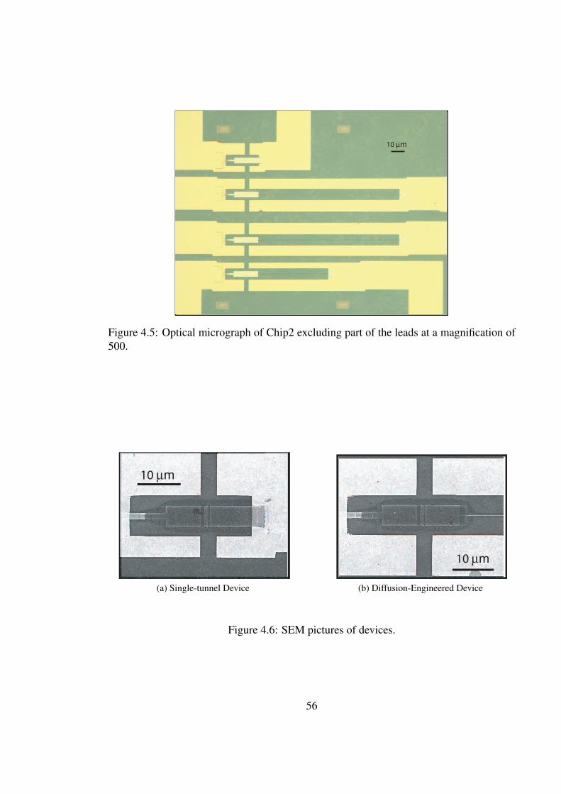
10 µm
Figure 4.5: Optical micrograph of Chip2 excluding part of the leads at a magnification of500.
10 µm
(a) Single-tunnel Device
10 µm
(b) Diffusion-Engineered Device
Figure 4.6: SEM pictures of devices.
56

Chapter 5
Experimental Results
This chapter presents experimental results from single-tunnel and diffusion-engineered de-
vices. The charge signal created by an absorbed photon in a diffusion-engineered device is
increased (via backtunnelling), compared to the charge signal created in a single-tunnelling
device by the same photon. Thus, using diffusion-engineering, single-photon resolution is
improved for photons in the UV and visible spectrum.
First I will describe how we developed the design for single UV-photon sensitive de-
vices, followed by data from an early design device tested at 50 mK. The expected re-
sponse of our devices to laser pulses will then be explained in detail. Before the presen-
tation of single UV photon measurements, I will explain how we control the Al diffusion
constant, which allows us to control the charge increase in the diffusion-engineered de-
vices (as explained in the theory chapter). I will then summarize the results and discuss
the improvement in the energy resolution attained with the diffusion-engineered devices.
5.1 Research Path
The implementation of the new diffusion-engineering approach for backtunnelling devices
benefitted from the availability of a reliable and high-resolution e-beam writer. The STJs
for previous research [Wilson2002] were fabricated using an optical lithography tri-layer
junction process, followed by wet etch patterning. The device geometries were set by the
pre-made optical masks, lacking the design dynamism associated with e-beam writing,
57

where one can adjust the device design with every patterning. In addition, optical lithogra-
phy and wet etching limited the minimum size of the junction to about 7 µm. As explained
at the end of the theory chapter, smaller area junctions have a smaller quiescent current
Idc, and therefore a smaller current noise in. Consequently, we used completely different
fabrication techniques then before, the most important ones being: e-beam lithography
instead of photolithography, and Dolan bridge double-angle deposition instead of tri-layer
tunnel junction technique. All junctions were designed to be 1× 5 µm2. The different
device generations are schematically illustrated in Figure 5.1 and optical micrographs of
real devices are shown in Figure 5.2.
We started the diffusion-engineering project by researching the reliability in the fab-
rication parameter space (described in the fabrication chapter by the junction fabrication
parameters) of e-beam Al junctions. We wanted to have a solid, reproducible junction
fabrication process for double-angle evaporation using e-beam lithography. We improved
our process by testing the devices cold, and analyzing their I(V) characteristics. In these
all-Al devices a good energy resolution was not expected.
Later, an absorber was defined by depositing Nb on top of one of the Al electrodes. Nb
had been found to have a high density of quasiparticle trapping centers, not being ideal as
a photon absorber. Our choice was forced by the fact that Ta sputtering gun in the Lesker
deposition system was broken at the time. None of these devices provided good enough
energy resolution for single UV photon detection.
5.1.1 Ta-absorber Devices
Once the Ta gun was fixed, we deposited Ta on a new wafer and started incorporating it into
our detectors’ design. We started with devices whose geometry is depicted in Figure 5.1a
having:
1. Ta absorber
2. Al junction overlapping Ta absorber
58

3. Ta absorber connected through a narrow Ta wire to the Al left pad
There was no photon-number resolution from the two tested single-tunnelling devices.
We thought the responsivity was too low due to quasiparticles escaping down the narrow
Ta wire and being trapped into the Al left pad.
Next generation (E04 Diff Ta6) of devices, shown in Figure 5.2a, included:
1. Ta absorber
2. Al junction overlapping Ta absorber
3. Nb contact from the Ta absorber to the Al left pad.
This design didn’t provide a better response of our junctions to UV photons. We real-
ized that the small Al trap volume necessary for a fast tunnelling time were not allowing
the quasiparticles to be trapped efficiently from the Ta absorber. Not having enough time to
relax down to the Al energy gap in the trap, the quasiparticles would diffuse back into the
Ta, and not tunnel across the junction. In the absorber, the quasiparticles would eventually
recombine and be lost.
Making the trap volume bigger to facilitate faster trapping would have increased the
tunnel time unless we made the junction larger, which would give a lower normal state
resistance. Having a larger junction would thus give a larger subgap current, and therefore
an associated larger current noise. One solution was to have the trap itself be the absorber.
5.1.2 Al-absorber Devices
The next design, shown schematically in Figure 5.1b had:
1. Al absorber (the two junction electrodes)
2. Ta ‘plug’ connected to Al wiring on the left and through a narrow Al wire to the left
electrode
After not having discriminated single photons, we decided to mask the whole device
except for the electrodes. We deposited a 200 nm SiO insulator and 100 nm Au on top, as
a reflector. The device (Aljct 1 R), with the Au mask on top, is shown in Figure 5.2b. We
59

were not able to bias the device due to electromagnetic cavity resonances we had created
by adding the mask. These resonances appeared as structure in the subgap I(V) curve.
Next we decided to have the wiring pads made out of Au, to better reflect photons
from areas outside the absorber. From the previous generation we also had proof of fast
device ageing (device gradually increasing its resistance within a week, until becoming
open). We thought this was due to a slowly degrading small-area interface. Since the
ageing process was common to all geometries, we reasoned the culprit must have been the
1×3 µm2 interface between the Ta plug and the Au pads. The geometry for these devices
is shown in Figure 5.1c, and Figure 5.2c shows a device picture.Thus we increased this
area by a factor of 15, as shown schematically in Figure 5.1d and in an optical micrograph
of a device in Figure 5.2d. This is the design we used for all the devices that had photon-
number resolution.
(a) Ta absorber with Al junction (b) Al absorber connected to Ta plug vianarrow Al wire
(c) Al absorber, small overlap between Taplug and Au pad
(d) Al absorber, larger overlap between Taplug and Au pad
Al Al junctionTa Au pads
Figure 5.1: Sketches of different device generation design [not to scale]. The scale is setby all the junctions being 1×5 µm2.
5.2 Dilution Refrigerator Measurements
Sample B−C2−T F from chip OPS−E03− ST J4B is an aluminum-only device, with
a normal resistance Rn = 93 Ω and an energy gap ∆ = 170 µeV at T = 50 mK. The two
60

Nb contact Ta absorber Junction
(a) E04 Diff Ta6 12 X150
Al electrodesAl wireTa plug
(b) Aljct 1 R Jct56 X150
(c) Aljct Aumirror Diff2 X150 (d) AP05 Diff1 3 1st X150
Figure 5.2: Consecutive device geometry generations.
5× 26 µm2 electrodes are terminated on one side by a 0.4× 360 µm2 narrow lead, and
on the other by a 5× 370 µm2 wider lead, as seen in Figure 5.3. It was the only device
measured in our Oxford dilution refrigerator, at a base temperature of 46 mK.
Only 2-wire dc measurements were performed. We investigated the variation of the
gap and of the critical current with an externally applied magnetic field parallel to the
junction barrier, and that of the subgap current with temperature.
A magnetic field parallel to the junction area should suppress the energy gap of a
superconductor. According to the Ginzburg-Landau theory of superconductivity, the gap
should decrease with magnetic field as in equation 5.1, disappearing when the field reaches
a critical value HC:
∆(H)∆(0)
=
√1−
(HHC
)2
(5.1)
61

Figure 5.3: Optical micrograph of sample B−C2−T F .
The measured the I(V) curves for different magnetic field values are shown in Fig-
ure 5.4.
-4
-2
0
2
4
I [µA
]
0.60.40.20.0-0.2-0.4 V [mV]
B = 700 G
B = 600 G
B = 500 G
B = 450 G
B = 400 G
B = 350 G
B =300 G
B = 250 G
B =200 G
B =100 G
B = 0 G
Figure 5.4: Measured I(V) curve at different magnetic field values, at 46 mK.
The fit of the data to equation 5.1 is shown in Figure 5.1. We obtain a critical field
HC = 510 G.
The first zero in the critical current occurred at a field B = 62 G, but the best suppres-
sion was achieved at the third zero B = 164 G, as seen in Figure 5.6.
The subgap current was recorded at different temperatures, as seen in Figure 5.7. This
was the first time the junctions fabricated in our group were measured at temperatures be-
low 215 mK. The critical current was nearly suppressed at the base temperature of 46 mK
62
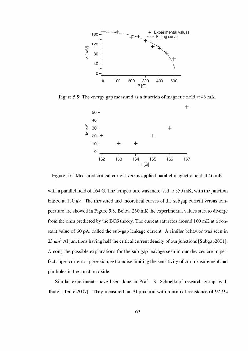
160
120
80
40
0
∆ [
µeV
]
5004003002001000
B [G]
Experimental values Fitting curve
Figure 5.5: The energy gap measured as a function of magnetic field at 46 mK.
50
40
30
20
10
0
Ic [
nA
]
167166165164163162
H [G]
Figure 5.6: Measured critical current versus applied parallel magnetic field at 46 mK.
with a parallel field of 164 G. The temperature was increased to 350 mK, with the junction
biased at 110 µV . The measured and theoretical curves of the subgap current versus tem-
perature are showed in Figure 5.8. Below 230 mK the experimental values start to diverge
from the ones predicted by the BCS theory. The current saturates around 160 mK at a con-
stant value of 60 pA, called the sub-gap leakage current. A similar behavior was seen in
23 µm2 Al junctions having half the critical current density of our junctions [Subgap2001].
Among the possible explanations for the sub-gap leakage seen in our devices are imper-
fect super-current suppression, extra noise limiting the sensitivity of our measurement and
pin-holes in the junction oxide.
Similar experiments have been done in Prof. R. Schoelkopf research group by J.
Teufel [Teufel2007]. They measured an Al junction with a normal resistance of 92 kΩ
63

6
4
2
0
-2
-4
I [n
A]
-200 -100 0 100 200
V [µV]
Data 46 mK
Data 255 mK
Data 294 mK
Data 336 mK
BCS 336mK BCS 294mK BCS 255mK BCS 46mK
Figure 5.7: Measured subgap current and the associated theoretical BCS curves for differ-ent temperatures.
and a gap of 225 µeV . The junction followed the BCS predictions down to about 170
mK [Prober2006].
0.001
0.01
0.1
1
10
I [n
A]
0.300.250.200.150.100.05
T [K]
Experimental data BCS current BCS current + 60 pA
Figure 5.8: Measured subgap current versus temperature. The junction has a normal resis-tance Rn = 93 Ω and the electrodes are terminated by a narrow lead on one side and by awider lead on the other. The fit includes an extra 60 pA of current added to the theoreticalBCS curve, an empirical procedure.
64
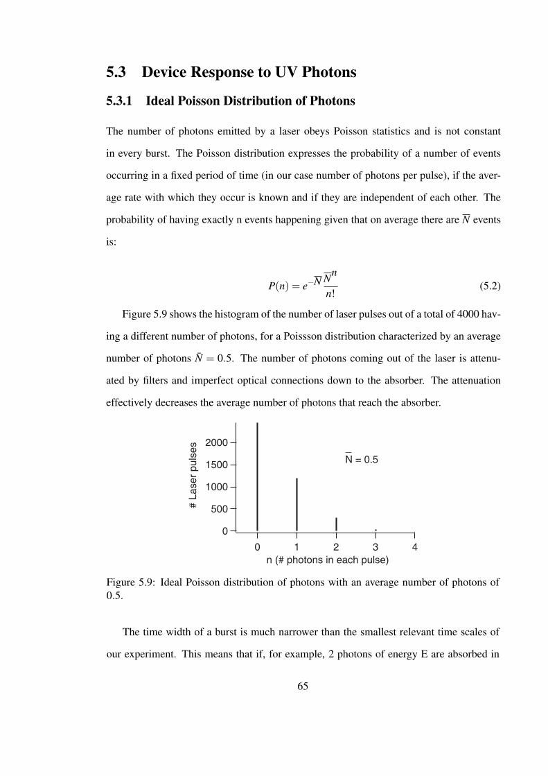
5.3 Device Response to UV Photons
5.3.1 Ideal Poisson Distribution of Photons
The number of photons emitted by a laser obeys Poisson statistics and is not constant
in every burst. The Poisson distribution expresses the probability of a number of events
occurring in a fixed period of time (in our case number of photons per pulse), if the aver-
age rate with which they occur is known and if they are independent of each other. The
probability of having exactly n events happening given that on average there are N events
is:
P(n) = e−N Nn
n!(5.2)
Figure 5.9 shows the histogram of the number of laser pulses out of a total of 4000 hav-
ing a different number of photons, for a Poissson distribution characterized by an average
number of photons N = 0.5. The number of photons coming out of the laser is attenu-
ated by filters and imperfect optical connections down to the absorber. The attenuation
effectively decreases the average number of photons that reach the absorber.
2000
1500
1000
500
0
# L
ase
r puls
es
43210
n (# photons in each pulse)
_ N = 0.5
Figure 5.9: Ideal Poisson distribution of photons with an average number of photons of0.5.
The time width of a burst is much narrower than the smallest relevant time scales of
our experiment. This means that if, for example, 2 photons of energy E are absorbed in
65

one pulse, the device will respond as if it had absorbed one photon of double the energy.
Assume the distribution of the number of pulses as a function of the number of photons in
each pulse that are absorbed in our devices is described by the average number N = 0.5.
Then the distribution of the number of pulses as a function of the charge in each pulse
will be characterized by the same average number N = 0.5. Thus the Poisson distribution
is mapped from the optical to the charge domain. This gives us in principle the possibil-
ity of testing our devices at any energy multiple of 3.68 eV. This is not true unless we
have a device whose absorber is the only photon-sensitive area. Increasing the number of
photons that land on the absorber also increases the number of photons that land on the
device’s wiring and on the substrate, which covers a much larger area than the absorber.
For each photon landing on the absorber, we have about 104 photons landing outside of
it, as explained in the setup chapter. These photons absorbed outside create substrate
phonons which couple to the detector and break an undetermined additional number of
Cooper pairs, creating excess noise. Thus for every laser pulse for which zero photons are
absorbed in our absorber, there is a non-zero number of photons landing close enough to
the junction to give a strong phonon signal. We read out this signal as a spurious pulse
with a finite charge, which we call the offset charge. Our devices lose their single-photon
resolution at an average number of around 5 absorbed photons.
For every detected charge Q, the noise in our detection system adds an uncertainty ∆Q
to it. The charge histogram of many pulses generated by the same number of photons will
have a Gaussian distribution. The full width half maximum (FWHM) of this distribution
determines the energy resolution of our measurement.
We exemplify the difference between the ideal Poisson distribution and our devices’
response to it in Figure 5.10. Each charge response has an associated width to it due mainly
to the noise in our system, amplifier noise and noise from photons absorbed outside the
absorber. The zero peak (n = 0) is shifted by an offset charge which is also due to photons
absorbed outside the absorber.
66

2000
1500
1000
500
0
# C
urr
en
t p
uls
es
100500
Pulse Charge [kilo electrons]
n=0
n=2
n=1
n=3
Charge offset
FWHM N=0.5
Figure 5.10: Non-ideal detection of an ideal Poisson distribution of photons with an aver-age number of photons of 0.5.
The charge histogram obtained from each run is fitted to a distribution formed of mul-
tiple Gaussians evenly spaced in charge:
P(Q) =∞
∑n=0
(e−N Nn
n!
)1√
2πσ2exp
(− 1
2σ2 (Q− (R×nEphoton +Q0)2))
(5.3)
There are several fit parameters in the distribution. The responsivity R measures how
many charge excitations were read out per unit energy of the incoming photon; the average
number of absorbed photons N; the standard deviation of the charge σ, which is translated
into an energy resolution via the responsivity; and the charge offset Q0, which is the av-
erage charge of the pulses recorded when there was no photon absorbed in our devices,
measured as the average charge of the peak n = 0 in the charge histogram.
5.3.2 Diffusion in Al
Having a material with a smaller diffusion constant lets us test devices with long outdif-
fusion times without increasing the number of squares in the outdiffusion lead. We can
achieve a smaller diffusion constant by increasing the oxygen impurities in the Al. This is
done by having a constant flow of oxygen in the deposition chamber during the Al evap-
67

oration. Table 5.1 presents results obtained by evaporating 50 nm of Al with different
oxygen concentrations in a 0.15× 30 µm2 trench. Assuming a rectangular cross-section,
the conductivity σ of the wire is σ = LRwt , where L, w and t are the wire’s length, width
and thickness, respectively. R is the normal state resistance measured just before the su-
perconducting transition. We use Einstein’s relation, σ = Nn(εF)e2D, to find the diffusion
constant D. Nn(εF) is the density of states per unit energy at the Fermi level in the metal1.
The conductivity of the sample can also be expressed as the inverse of the resistivity ρ.
For the first and last sample the transition temperature was not recorded.
Oxygen flow Pressure during evaporation ρ Dn TC[sccm] [T]×10−5 [µΩ cm] [cm2/s] [K]
0.4 1.5 20 9.0 −0.5 2 72 2.5 1.960.6 2.2 155 1.2 2.11
0.75 2.5 266 0.7 2.190.8 4.1 386 0.47 −
Table 5.1: Al film parameters as a function of the O2 concentration during evaporation.
8
6
4
2
Diffu
sio
n c
on
sta
nt
[cm
2/s
]
0.80.70.60.50.4
Oxygen flow [sccm]
350
300
250
200
150
100
50
Resis
tivity
[µΩ
cm
]
Diffusion constant Resisitivty
Figure 5.11: Diffusion constant D and resistivity ρ as a function of oxygen flow during Aldeposition. Devices fabricated and measured by F. Pierre, C. Rigetti, and C. M. Wilson atYale University.
1We are using here the density of states at the Fermi level as found in [Anthore2003], N(εF) = 2.15×1047
states/(Jm3).
68
In the superconducting state, the quasiparticle diffusion constant is reduced compared
to its normal state value. This is due to the quasiparticle dispersion relation exhibiting a
minimum at the Fermi energy, where the density of states diverges. This approach of the
quasiparticle group velocity to zero dictates a smaller superconducting diffusion constant,
which for thermal equilibrium has been computed by [Narayanamurti1978] to be:
Dqp = Dn
√2kBTπ∆
(5.4)
5.3.3 Aluminum Devices with ∆ = 170 µeV (Chip1)
Our ‘clean’ Al devices had the Al electrodes deposited in high-vacuum, in the absence of
oxygen. The parameters for these devices are shown in Appendix B. The junctions had an
energy gap ∆ = 170 µeV and a normal state resistance Rn = 133 Ω. The types of devices
tested were: single tunnel device (Chip1 st), ‘short diffusion-engineered’ device with a
0.25× 62 µm2 outdiffusion lead (Chip1 sd), and ‘long diffusion-engineered’ device with
a 0.25×125 µm2 outdiffusion lead (Chip1 ld).
The optical testing of the single tunnel device was done using a room temperature, 1
MΩ feedback resistor, which added extra Johnson current noise to the measurements. A
1 MΩ cold resistor was used for the feedback, but the electrical connections to it were
unstable during that measurement. This in conjunction with temporary and unusual elec-
trical interference from the laser significantly decreased the sensitivity of the device. The
pulses from the laser photons had a characteristic decay time of 4.9 µs, and an estimated
responsivity of 1200 electrons/eV.
The other two types of devices were measured with a cold feedback resistor and no
electrical interference from the laser. Figure 5.12 shows the current vs. voltage character-
istics of Chip1 sd and Chip1 ld after the critical current was optimally suppressed in each
device. The deviation from the BCS shape for Chip1 sd is probably due to imperfect sup-
pression of the critical current, which can be due to non-uniformities in the oxide barrier.
69

Chip1 ld shows a deviation from the BCS shape in the opposite direction. This can be an
averaging effect of the voltage bias, if there is noise below 1 nA.
4
3
2
1
0
I [n
A]
200150100500
V [µV]
Chip1_sd Chip1_ld Chip1_sd_BCS T = 0.31 K Chip1_ld_BCS T = 0.30 K
Figure 5.12: Current vs. voltage characteristic of the ∆ = 170 µeV devices.
We biased both devices around 110 µV and recorded 4000 pulses for several light in-
tensities (i.e. different average photon numbers). Figure 5.13 shows the histogram of the
integrated pulse charge for 3 different intensities. The no-photon case, when the laser
optical shutter is closed, tests how much of the energy distribution is due to the noise in-
dependent of the photon flux. The average pulse from Chip1 sd has a characteristic decay
time of 10.7 µs and a responsivity of 2330 electrons/eV. The long-diffusion engineered
device, Chip1 ld, had a lower responsivity of 1840 electrons/eV, associated with a shorter
pulse decay time of 9.6 µs.
The best energy resolution ∆E = 1.65 eV was obtained with Chip1 ld. The energy
distribution for both devices tested with the cold feedback resistor widened as the light
intensity increases, as shown in Figure 5.14.
The charge offset represents the average integrated charge of the pulses recorded when
no photons landed on the absorber. This variable is proportional to the light intensity, just
like the energy distribution width. Figure 5.15 displays the measured charge offset for
different light intensities, for both diffusion-engineered devices.
70

140
120
100
80
60
40
20
0
# C
ou
nts
/ b
in
60x10-3
40200
Charge [kilo electrons]
Experimental data - no photons
Experimental data N = 0.6
Experimental data for N = 2.2
Fits to data
Long diffusion-engineered device
(Chip1_ld)
Figure 5.13: Pulse histograms for the clean Al, long diffusion-engineered device, tested atdifferent light intensities, each corresponding to a different average photon number of thePoisson distribution.
5.3.4 Aluminum Devices with ∆ = 225 µeV (Chip2)
In order to obtain a smaller diffusion constant, we fabricated devices where the Al was de-
posited in the presence of oxygen. This Al is what we refer to as ‘dirty’ Al. The parameters
for these devices are shown in Appendix B. The devices had a gap energy ∆ = 225 µeV
and a normal state resistance Rn = 90 Ω. We tested three types of devices: single tunnel
device (Chip2 st), ‘short diffusion-engineered’ device with a 0.25× 62 µm2 outdiffusion
lead (Chip2 sd), and ‘long diffusion-engineered’ device with a 0.25× 125 µm2 outdiffu-
sion lead (Chip2 ld).
The current vs. voltage characteristics of all three devices after the critical current has
been optimally suppressed are shown in Figure 5.16. We notice the imperfect suppression
of the critical current in all three devices.
The long diffusion-engineered device was tested in a slightly different setup, shown
in Figure 5.17. We fabricated a mechanical mask by depositing 100 nm Au with a 3
71

16
14
12
10
8
6
4
2
EF
WH
M2 [eV
2]
543210
Average number of photons
Short diffusion-engineered device
Long diffusion-engineered device
∆
Figure 5.14: FWHM of the energy distribution for the ∆ = 170 µeV devices.
nm seed layer of Ti on a glass slide. The Au covered a 0.4× 1.6 µm2 area, except for
a central 61× 130 µm2 rectangle which remained transparent. The glass slide was diced
into a 0.6×1.6 mm2 rectangle. Two small pieces of the same glass slide were glued with
GE-varnish on the top and bottom of the device chip, but far away from the detectors. The
diced Au mask was placed on top of the two glued pieces, preventing the scratching of the
device. It was then manually aligned such that the central transparent rectangle would sit
on top of the detectors.
Laser pulses were recorded and analyzed for all three devices. Chip2 st had a respon-
sivity of 1500 electrons/eV (5500 electrons/photon). The average pulse had a character-
istic decay time τ = 4.3 µs. Chip2 sd showed a larger responsivity, 3500 electrons/eV,
as well as a longer decay time τ = 9.1 µs. The device with the outdifussion lead twice
as long as the one of Chip2 sd, Chip2 ld, had an intermediate value of its average pulse
characteristic decay time, between that of the single-tunnel and that of the short-diffusion
engineered devices, τ = 6.8 µs. Its responsivity was 2330 electrons/eV. Histograms from
all three devices are shown in Figure 5.18, for the same number of average photons.
The offset charge Q0 increased linearly with the tested flux of incoming photons. The
72

60x103
50
40
30
20
10
0
Offse
t ch
arg
e [
ele
ctr
on
s]
543210
Average number of photons
Short diffusion-engineered device
Long diffusion-engineered device
Figure 5.15: Charge offset vs. average number of photons for the ∆ = 170 µeV devices.
8
6
4
2
0
I [n
A]
200150100500
V [µV]
Chip2_st Chip2_sd Chip2_ld
Figure 5.16: Current vs. voltage characteristic of the ∆ = 225 µeV devices.
three devices show different slopes, seen in figure 5.19.
The best energy resolution was obtained for Chip2 sd, ∆E = 1.23 eV. Chip2 ld had
∆E = 1.72 eV, followed by Chip2 st with ∆E = 1.8 eV. The FWHM of the energy distri-
bution increased with N for all devices.
Chip2 ld is the only device tested with photons from the Hg lamp. A violet filter
allowed only photons of 2.85 eV of energy to be absorbed by the device. The signal
trigger was set at a voltage equivalent to a 0.3 nA current. Most recorded pulses do not
peak above 0.3 nA. This means that the average charge of the acquired pulses sets an
73
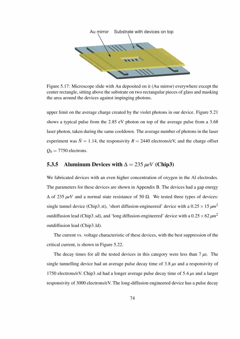
Au mirror Substrate with devices on top
Figure 5.17: Microscope slide with Au deposited on it (Au mirror) everywhere except thecenter rectangle, sitting above the substrate on two rectangular pieces of glass and maskingthe area around the devices against impinging photons.
upper limit on the average charge created by the violet photons in our device. Figure 5.21
shows a typical pulse from the 2.85 eV photon on top of the average pulse from a 3.68
laser photon, taken during the same cooldown. The average number of photons in the laser
experiment was N = 1.14, the responsivity R = 2440 electrons/eV, and the charge offset
Q0 = 7750 electrons.
5.3.5 Aluminum Devices with ∆ = 235 µeV (Chip3)
We fabricated devices with an even higher concentration of oxygen in the Al electrodes.
The parameters for these devices are shown in Appendix B. The devices had a gap energy
∆ of 235 µeV and a normal state resistance of 50 Ω. We tested three types of devices:
single tunnel device (Chip3 st), ‘short diffusion-engineered’ device with a 0.25×15 µm2
outdiffusion lead (Chip3 sd), and ‘long diffusion-engineered’ device with a 0.25×62 µm2
outdiffusion lead (Chip3 ld).
The current vs. voltage characteristic of these devices, with the best suppression of the
critical current, is shown in Figure 5.22.
The decay times for all the tested devices in this category were less than 7 µs. The
single tunnelling device had an average pulse decay time of 3.8 µs and a responsivity of
1750 electrons/eV. Chip3 sd had a longer average pulse decay time of 5.4 µs and a larger
responsivity of 3000 electrons/eV. The long-diffusion engineered device has a pulse decay
74
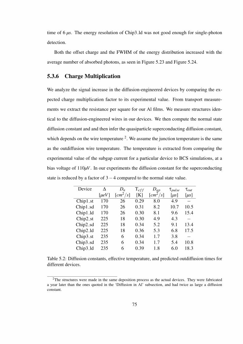
time of 6 µs. The energy resolution of Chip3 ld was not good enough for single-photon
detection.
Both the offset charge and the FWHM of the energy distribution increased with the
average number of absorbed photons, as seen in Figure 5.23 and Figure 5.24.
5.3.6 Charge Multiplication
We analyze the signal increase in the diffusion-engineered devices by comparing the ex-
pected charge multiplication factor to its experimental value. From transport measure-
ments we extract the resistance per square for our Al films. We measure structures iden-
tical to the diffusion-engineered wires in our devices. We then compute the normal state
diffusion constant and and then infer the quasiparticle superconducting diffusion constant,
which depends on the wire temperature 2. We assume the junction temperature is the same
as the outdiffusion wire temperature. The temperature is extracted from comparing the
experimental value of the subgap current for a particular device to BCS simulations, at a
bias voltage of 110µV . In our experiments the diffusion constant for the superconducting
state is reduced by a factor of 3−4 compared to the normal state value.
Device ∆ Dn Te f f Dqp τpulse τout[µeV ] [cm2/s] [K] [cm2/s] [µs] [µs]
Chip1 st 170 26 0.29 8.0 4.9 −Chip1 sd 170 26 0.31 8.2 10.7 10.5Chip1 ld 170 26 0.30 8.1 9.6 15.4Chip2 st 225 18 0.30 4.9 4.3 −Chip2 sd 225 18 0.34 5.2 9.1 13.4Chip2 ld 225 18 0.36 5.3 6.8 17.5Chip3 st 235 6 0.34 1.7 3.8 −Chip3 sd 235 6 0.34 1.7 5.4 10.8Chip3 ld 235 6 0.39 1.8 6.0 18.3
Table 5.2: Diffusion constants, effective temperature, and predicted outdiffusion times fordifferent devices.
2The structures were made in the same deposition process as the actual devices. They were fabricateda year later than the ones quoted in the ‘Diffusion in Al’ subsection, and had twice as large a diffusionconstant.
75

We use the geometrical dimensions of our devices and the superconducting diffusion
constant into the 2D diffusion simulation to extract the outdiffusion time τout . The out-
diffusion time is computed as the time it takes 67% of the quasiparticles to leave the
electrodes and wire area, including a certain loss (recombination) time. Table 5.2 shows
the above parameters for our devices, including a loss time of 20 µs in the simulation for
the outdiffusion time and the measured decay time of the pulses τpulse.
We see that a recombination time of 20 µs is compatible with the results from Chip1 sd
device, while a shorter loss time would be consistent with the times obtained for Chip2
and Chip3 devices. Even within the same material type devices (such as devices on Chip1,
Chip2, or Chip3) assuming the same loss time does not provide consistent results among
the diffusion-engineered samples. This implies the possibility of a loss time related to the
length of the outdiffusion lead. This could be the case if there were depressed-gap regions
along the lead, which would facilitate quasiparticle trapping.
In Figure 5.25 we summarize our results. The simulated charge multiplication factor,
psim, is computed as the ratio of the simulated outdiffusion time to the experimental tun-
nelling time. The ratio of the experimental pulse decay time for the diffusion-engineered
devices to the tunnelling time is presented, along with the experimental charge gain fac-
tor (Q/Qi). The two experimental ratios agree well with each other, as expected, but the
number of times the quasiparticles tunnel does not exceed 2 in any of the devices. This
discrepancy from the expected behavior is indicative of strong losses in our materials.
5.4 Summary
We succesfully tested single-tunnelling and diffusion-engineered devices with single UV
photon resolution. The diffusion-engineered samples provided charge gain upon absorp-
tion of photons due to backtunnelling, compared to the single-tunnelling samples. The
charge multiplication technique could not be tested to factors larger than 2.3 due to a rela-
tively short loss time in our devices, on the order of 20 µs.
76

120
80
40
0
# C
ou
nts
/ b
in
50x10-3
403020100
Charge [kilo electrons]
R = 5500 electrons/photon
Experimental data
Fit to data
Single tunneling device
(Chip2_st)
160
120
80
40
0# C
ou
nts
/ b
in
50x10-3
403020100
Charge [kilo electrons]
R = 13000 electrons/photon
Experimental data
Fit to data
Short diffusion-engineered device
(Chip2_sd)
120
80
40
0
# C
ou
nts
/ b
in
50x10-3
403020100Charge [kilo electrons]
R = 8600 electrons/photon
Experimental data
Fit to data
Long diffusion-engineered device
(Chip2_ld)
Figure 5.18: Pulse histograms from three different devices under laser testing. The averagenumber of photons per pulse was around 0.5 for all.
77

50x103
40
30
20
10
0
Offse
t ch
arg
e [
ele
ctr
on
s]
3.02.52.01.51.00.50.0
Average number of photons
Single tunnel deviceShort diffusion-engineered device Long diffusion-engineered device
Figure 5.19: Charge offset Q0 vs. average number of photons N for the ∆ = 225 µeVdevices.
16
14
12
10
8
6
4
2
EF
WH
M2 [
eV
2]
3.02.52.01.51.00.50.0
Average number of photons
Single tunnelling device Short diffusion-engineered device Long diffusion-engineered device
∆
Figure 5.20: FWHM of the energy distribution for the ∆ = 225 µeV devices.
78

500
400
300
200
100
0
-100
Cu
rre
nt
[pA
]
100x10-6
806040200
Time [s]
Violet photon pulse
UV photon average pulse (N = 1.14)
Figure 5.21: Violet photon single pulse and UV photons average pulse.
35
30
25
20
15
10
5
0
I [
nA
]
200150100500
V [µV]
Chip3_st Chip3_sd
Figure 5.22: Current vs. voltage characteristic of the ∆ = 235 µeV devices.
79

20x103
16
12
8
4
Offse
t ch
arg
e [
ele
ctr
on
s]
0.50.40.30.2
Average number of photons
Single tunneling device
Short diffusion-engineered device
Figure 5.23: Charge offset vs. average number of photons for the ∆ = 235 µeV devices.
16
14
12
10
8
6
4
2
EF
WH
M2 [
eV
2]
0.50.40.30.2
Average number of photons
Single tunnelling device
Short diffusion-engineered device
∆
Figure 5.24: FWHM of the energy distribution for the ∆ = 235 µeV devices.
80

Figure 5.25: Results.
81

Chapter 6
Conclusions
6.1 Diffusion Engineering Review
We have developed an STJ-based spectrometer with single photon resolution in the UV
spectrum. Previous work in our group used gap engineering to intrinsically amplify the
signal created by an absorbed photon, using backtunnelling. The performance of those
devices was limited by the generation-recombination noise [Wilson2001] of the quasipar-
ticles confined in the Al electrodes by higher-gap Ta plugs.
We implemented a new approach, called diffusion engineering. In this approach the
junction electrode terminates with a long and narrow lead that prevents quasiparticles from
quickly diffusing away. The quasiparticles tunnel and backtunnel across the voltage-biased
junction before they slowly diffuse out the lead or get lost through recombination or other
loss mechanisms.
We designed, fabricated and tested single-tunnelling devices and devices with different
outdiffusion lead lengths. We used 1× 5 µm2 Al/AlOx/Al junctions, with 5× 10 µm2 Al
electrodes, which also functioned as the absorber. We fabricated Al films of different
qualities, thus changing the diffusion constant in the outdiffusion lead, and therefore the
outdiffsion time.
82
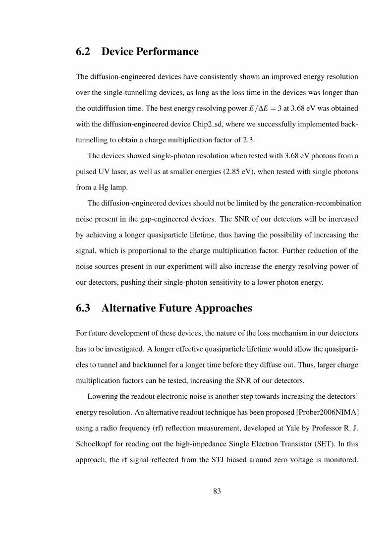
6.2 Device Performance
The diffusion-engineered devices have consistently shown an improved energy resolution
over the single-tunnelling devices, as long as the loss time in the devices was longer than
the outdiffusion time. The best energy resolving power E/∆E = 3 at 3.68 eV was obtained
with the diffusion-engineered device Chip2 sd, where we successfully implemented back-
tunnelling to obtain a charge multiplication factor of 2.3.
The devices showed single-photon resolution when tested with 3.68 eV photons from a
pulsed UV laser, as well as at smaller energies (2.85 eV), when tested with single photons
from a Hg lamp.
The diffusion-engineered devices should not be limited by the generation-recombination
noise present in the gap-engineered devices. The SNR of our detectors will be increased
by achieving a longer quasiparticle lifetime, thus having the possibility of increasing the
signal, which is proportional to the charge multiplication factor. Further reduction of the
noise sources present in our experiment will also increase the energy resolving power of
our detectors, pushing their single-photon sensitivity to a lower photon energy.
6.3 Alternative Future Approaches
For future development of these devices, the nature of the loss mechanism in our detectors
has to be investigated. A longer effective quasiparticle lifetime would allow the quasiparti-
cles to tunnel and backtunnel for a longer time before they diffuse out. Thus, larger charge
multiplication factors can be tested, increasing the SNR of our detectors.
Lowering the readout electronic noise is another step towards increasing the detectors’
energy resolution. An alternative readout technique has been proposed [Prober2006NIMA]
using a radio frequency (rf) reflection measurement, developed at Yale by Professor R. J.
Schoelkopf for reading out the high-impedance Single Electron Transistor (SET). In this
approach, the rf signal reflected from the STJ biased around zero voltage is monitored.
83

The reflected signal depends on the STJ impedance around zero bias, which provides a
very sensitive measure of the number of excess quasiparticles. A resonant readout is used,
opening the possibility of frequency multiplexing several STJs in an efficient fashion.
Testing devices at lower temperatures than those tested in this work would also be ben-
eficial for achieving a higher energy resolving power, by decreasing the Johnson current
noise of the STJ. Once the detector resolution is limited by statistical noise, lower-gap ma-
terials should be used as the absorber. This would increase the SNR as the square root of
∆−1, although the relaxation time for quasiparticles becomes longer, which is detrimental
to the photon counting rate and increases the importance of any loss in the materials.
84

Appendix A
Film Properties
The Ta thicknesses on wafers E04 and AP05 are 85 nm and 70 nm respectively. The
aluminum films on Al1 and Al2 was deposited in the Plassys in the presence of 0.4 sccm
of oxygen. Both films had a first 50 nm layer deposited (thickness perpendicular to the
substrate) at a 40 angle from the normal; this was oxidized at the parameters listed below;
then a second 70 nm layer was deposited normal to the surface. The oxidation parameters
for the two films are: 20 Torr for 12 min for Al1; 3 Torr for 10 minutes for Al2. The
resistance for the Al films was measured for both films, with the total thickness of 120 nm,
and the oxide layer in between.
85

Film type Dimensions [µm2] Resistance @ 300 K [Ω] RRR R/square [Ω]1×20 61.6 7.3 3
Ta [wafer E04] 1×30 82.4 7.0 3TC = 4.4 K 2×20 38.4 7.1 3d = 85 nm 2×40 59 7 3
0.15×4.5 103 4.12 3Ta [wafer E04] 0.3×6 62.5 6.25 3
TC = 4.4 K 0.3×9 115 4.6 3d = 85 nm 0.3×12 136 5.4 3
2.3×140 309.2 4.12 1.64Ta [wafer AP05] 2.4×100 231.2 6.25 1.87
TC = 4.05 K 2.3×140 323.5 4.6 1.73d = 70 nm 2.3×170 390.6 5.4 1.71
Al 1 2.2×160 62.3 0.86 120 Torr×12 min 2.2×120 52.9 0.95 1
Al 2 0.25×60 248 1.3 0.853 Torr×10 min 0.25×120 529 1.3 0.85
Table A.1: Properties of Ta and Al films.
86
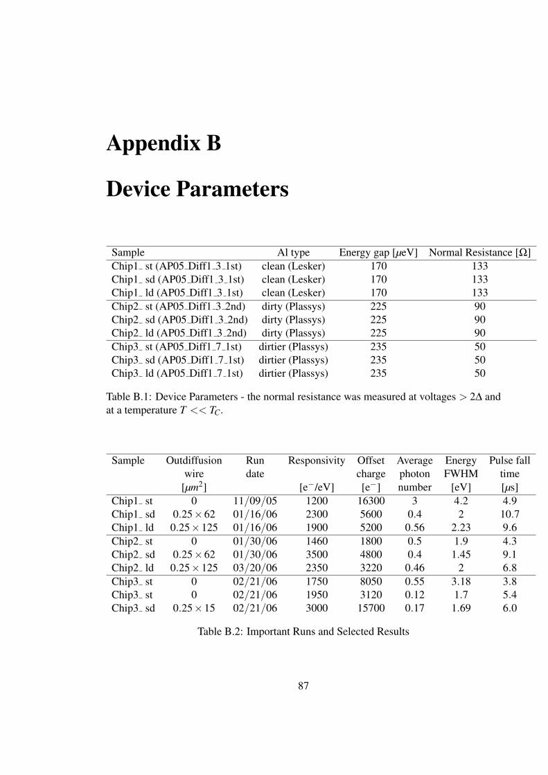
Appendix B
Device Parameters
Sample Al type Energy gap [µeV] Normal Resistance [Ω]Chip1 st (AP05 Diff1 3 1st) clean (Lesker) 170 133Chip1 sd (AP05 Diff1 3 1st) clean (Lesker) 170 133Chip1 ld (AP05 Diff1 3 1st) clean (Lesker) 170 133Chip2 st (AP05 Diff1 3 2nd) dirty (Plassys) 225 90Chip2 sd (AP05 Diff1 3 2nd) dirty (Plassys) 225 90Chip2 ld (AP05 Diff1 3 2nd) dirty (Plassys) 225 90Chip3 st (AP05 Diff1 7 1st) dirtier (Plassys) 235 50Chip3 sd (AP05 Diff1 7 1st) dirtier (Plassys) 235 50Chip3 ld (AP05 Diff1 7 1st) dirtier (Plassys) 235 50
Table B.1: Device Parameters - the normal resistance was measured at voltages > 2∆ andat a temperature T << TC.
Sample Outdiffusion Run Responsivity Offset Average Energy Pulse fallwire date charge photon FWHM time
[µm2] [e−/eV] [e−] number [eV] [µs]Chip1 st 0 11/09/05 1200 16300 3 4.2 4.9Chip1 sd 0.25×62 01/16/06 2300 5600 0.4 2 10.7Chip1 ld 0.25×125 01/16/06 1900 5200 0.56 2.23 9.6Chip2 st 0 01/30/06 1460 1800 0.5 1.9 4.3Chip2 sd 0.25×62 01/30/06 3500 4800 0.4 1.45 9.1Chip2 ld 0.25×125 03/20/06 2350 3220 0.46 2 6.8Chip3 st 0 02/21/06 1750 8050 0.55 3.18 3.8Chip3 st 0 02/21/06 1950 3120 0.12 1.7 5.4Chip3 sd 0.25×15 02/21/06 3000 15700 0.17 1.69 6.0
Table B.2: Important Runs and Selected Results
87

Bibliography
[Anthore2003] A. Anthore, H. Pothier, and D. Esteve. Density of states in a
superconductor carrying a supercurrent. Physical Review Letters,
90(12):127001, 2003.
[BCS1957] J. Bardeen, L. N. Cooper, and J. R. Schrieffer. Theory of superconduc-
tivity. Physical Review, 108(5).
[Booth1987] N. E. Booth. Quasiparticle trapping and the quasiparticle multiplier.
Applied Physics Letters, 50:293, 1987.
[Bruijne2002] J. H. J. de Bruijne, A. P. Reynolds, M. A. C. Perryman, A. Peacock,
F. favata, N. Rando, D. Martin, P. Verhoeve, and N. Christlieb. Direct
determination of quasar redshifts. Astronomy and Astrophysics, 381,
2002.
[Dolan1977] G. J. Dolan. Offset masks for lift-off photoprocessing. Applied Physics
Letters, 31(5):337, 1977.
[Ehrenreich1963] H. Ehrenreich, H. R. Philipp, and B. Segall. Optical properties of alu-
minum. Physical Review, 132(5):1918, 1963.
[Friedrich1997] Stephan Friedrich. Superconducting single photon imaging X-ray spec-
trometers. PhD thesis, Yale University, 1997.
[Friedrich97IEEE] S. Friedrich, K. Segall, M. C. Gaidis, C. M. Wilson, D. E. Prober,
P. J. Kindlemann, A. E. Szymkowiak, and S. H. Moseley. Single pho-
88

ton imaging X-ray spectrometers using low noise current preamplifiers
with dc voltage bias. IEEE Transactions on Applied Superconductivity,
7(2):3383, 1997.
[Gaidis1994] Michael Gaidis. Superconducting tunnel junctions as single photon X-
ray detectors. PhD thesis, Yale University, 1994.
[Goldie1994] D. J. Goldie, P. L. Brink, C. Patel, N. E. Booth, and G. L. Salmon.
Statistical noise due to tunneling in superconducting tunnel junctions.
Applied Physics Letters, 64:3169, 1994.
[Golubov1994] A. A. Golubov, E. P. Houwman, J. G. Gijsbertsen, J. Flokstra,
and H. Rogalla. Quasiparticle lifetimes and tunneling times in a
superconductor-insulator-superconductor tunnel junction with spatially
inhomogeneous electrodes. Phsical Review B, 49(18):12953, 1994.
[Gray1978] K. E. Gray. A superconducting transistor. Applied Physics Letters,
32:392, 1978.
[Kaplan1976] S. B. Kaplan, C. C. Chi, and D. N. Langenberg. Quasiparticle and
phonon lifetimes in superconductors. Physical Review B, 14(11):4854,
1976.
[Kittel] C. Kittel. Introduction to Solid State Physics. John Wiley and Sons,
Inc.
[Kozorezov2000] A. G. Kozorezov, A. F. Volkov, J. K. Wigmore, A. Peacock, A. Poelaert,
and R. den Hartog. Quasiparticle-phonon downconversion in nonequi-
librium superconductors. Physical Review B, 61(17):807, 2000.
89
[Kurakado1982] M. Kurakado. Possibility of high resolution detectors using supercon-
ducting tunnel junctions. Nuclear Instruments and Methods, 196:275,
1982.
[LSM510] Carl Zeiss, Inc. Meta laser scanning microscope 510 data sheet.
[Li2002] Liqun Li. X-ray Single Photon Imaging Detectors using Superconduct-
ing Tunnel Junctions. PhD thesis, Yale University, 2002.
[McMillan1966] W. L. McMillan and P. W. Anderson. Theory of geometrical resonances
in the tunneling charcateristics of thick films in superconductors. Phys-
ical Review Letters, 16(3):85, 1966.
[Nagl2005] S. Nagl, M. Schaeferling, and O. S. Wolfbeis. Fluorescence analisys in
microarray technology. Microchimica Acta, 151:1, 2005.
[Narayanamurti1978] V. Narayanamurti, R. C. Dynes, P. Hu, H. Smith, and W. F.
Brinkman. Quasiparticle and phonon propagation in bulk, supercon-
ducting lead. Physical Review B, 18(11).
[Prober2006] Invited Talk by Daniel Prober at the Applied Superconductivity Confer-
ence in Seattle. Ultra-sensitive quantum-limited far-infrared stj detec-
tors, http://www.yale.edu/proberlab/stj.html. 2006.
[Prober2006NIMA] D. E. Prober, J. D. Teufel, L. Frunzio, C. M. Wilson, and R. J.
Schoelkopf. Quasiparticle dynamics and a new, high-resolution read-
out of stj photon detectors. Nuclear Intruments and Methods in Physics
Research A, 559:676, 2006.
[Rando1992] N. Rando, A. Peacock, A. van Dordrecht, C. Foden, R. Engelhardt,
B. G. Taylor, P. Gare, J. Lumley, and C. Pereira. The properties of nio-
bium superconducting tunneling junctions as X-ray detectors. Nuclear
90

Instruments and Methods in Physics Research Section A: Accelerators,
Spectrometers, Detectors and Associated Instruments, 313:173, 1992.
[Rando2000] N. Rando, S. Andersson, B. Collaudin, F. Favata, P. Gondoin, A. Pea-
cock, M. Perryman, J. Verveer, P. Verhoeve, and D. J. Goldie. First
astronomical results from S-Cam. Nuclear Instruments and Methods
in Physics Research Section A: Accelerators, Spectrometers, Detectors
and Associated Instruments, 444(1):441, 2000.
[Rothwarf1967] A. Rothwarf and B. N. Taylor. Measurement of recombination lifetimes
in superconductors. Physical Review Letters, 19(1):27, 1967.
[Segall2000] Kenneth Segall. Noise and Quasiparticle Dynamics in Single Photon,
Superconducting Tunnel Junctions Detectors. PhD thesis, Yale Univer-
sity, 2000.
[Segall2004] K. Segall, C. Wilson, L. Li, S. Friedrich, M. C. Gaidis, and D. E. Prober.
Dynamics and energy distribution of nonequilibrium quasiparticles in
superconducting tunnel junctions. Physical Review B, 70:214520, 2004.
[Subgap2001] M. A. Gubrud, M. Ejrnaes, A. J. Berkley, R. C. Ramos Jr., I. Jin, J. R.
Anderson, A. J. Dragt, C. J. Lobb, and F. C. Wellstood. Sub-gap leakage
in nb/alox/nb and al/alox/al josephson junctions. IEEE Transaction on
Applied superconductivity, 11(1):1002, 2001.
[Teufel2007] John Teufel. Superconducting Tunnel Junctions as Direct Detectors for
Submillimeter Astronomy. PhD thesis, Yale University, 2007.
[Tinkham1972] Michael Tinkham. Tunneling generation, relaxation, and tunneling de-
tection of hole-electron imbalance in superconductors. Physical Review
B, 6:1747, 1972.
91
[Tomasch1966] W. J. Tomasch. Geometrical resonance and boundary effects in tunnel-
ing from superconducting In. Physical Review Letters, 16(1):16, 1966.
[Twerenbold1986] D. Twerenbold. Nonequilibrium model of the superconducting tunnel-
ing junction X-ray detector. Physical Review B, 34(11):7748, 1986.
[VanDuzer1981] T. Van Duzer and C. W. Turner. Principles of superconductive devices
and circuits. Elsevier, 1981.
[Verhoeve2006] P. Verhoeve, D. Martin, R. A. Hijmering, J. Verveer, A. van Dordrecht,
G. Sirbi, T. Oosterbroek, and A. Peacock. S-Cam 3: Optical astronomy
with a STJ-based imaging spectrophotometer. Nuclear Instruments and
Methods in Physics Research A, 559:598, 2006.
[Weaver1974] J. H. Weaver, D. W. Lynch, and C. G. Olson. Optical properties of V,
Ta, and Mo from 0.1 to 35 eV. Physical Review B, 10(2):501, 1974.
[Wilson2001] C. M. Wilson, L. Frunzio, and D. E. Prober. Time-resolved measure-
ments of thermodynamic fluctuations of the particle number in a non-
degenerate fermi gas. Physical Review Letters, 87(6):067004, 2001.
[Wilson2002] Christopher M. Wilson. Optical/UV single-photon spectrometers using
superconducting tunnel junctions. PhD thesis, Yale University, 2002.
92
Related Documents