Thin Solid Films, 112 (1984)51- 59 PREPARATION AND CHARACTERIZATION 51 THE INFLUENCE OF DEPOSITION PARAMETERS ON THE PROPERTIES OF AMORPHOUS SILICON THIN FILMS PRODUCED BY THE MAGNETRON SPUTTERING METHOD A. K. BATABYAL, P. CHAUDHURI, SWATI RAY AND A. K. BARUA Indian Association for the Cultivation of Science, Calcutta 700032 (India) (Received June 15, 1983; accepted October 14, 1983) The influence of various deposition parameters on the properties of amorphous silicon (a-Si) thin films produced by r.f. magnetron sputtering was studied. The following parameters were varied: the incident r.f. power, the argon pressure in the sputtering chamber and the substrate temperature. The films were characterized by studying the dark conductivity and optical absorption from which the values of the band gaps were obtained. The most interesting result was that a-Si films prepared at high argon pressures showed significant photoconductivity. The results show that the magnetron sputtering method has good potential for producing high quality a-Si films. 1. INTRODUCTION Hydrogenated amorphous silicon (a-Si:H) thin films produced by the r.f.-d.c. glow discharge of silane gas have proved to be very promising materials for the fabrication of solar cells and other devices 1. An alternative method of preparing a-Si:H films which has been successfully applied to device fabrication2 is the r.f. sputtering technique in which silicon is sputtered using a mixture of argon and hydrogen gases. The fact that the sputtering method has been comparatively less successful than the glow discharge method is believed to be a result of damage to the a-Si:H film during sputtering resulting in a higher defect density. However, efforts are being made to improve the quality of the sputtered a-Si: H films. A number of investigations of the properties of a-Si films prepared by r.f. diode sputtering have been reported 3-11. Most of the detailed studies have concentrated on a-Si:H films. However, investigations of the influence of various deposition parameters on the properties of unhydrogenated a-Si films have been reported by Pawlewicz 4, Shimizu and coworkers 9' ~ 0 and Imura et al. 1 x In a conventional diode sputtering system the secondary electrons from the target, which are accelerated across the cathode dark space and hit the substrate, constitute a major source of radiation damage. In the magnetron sputtering method the secondary electrons are trapped in the tunnel magnetic field near the target and hence the damage to the film is likely to be less. In view of this advantage we have undertaken a programme for the preparation and characterization of magnetronzsputtered a-Si:H films. In this paper we report the results of investigations of the dependence of the properties of 0040-6090/84/$3.00 © Elsevier Sequoia/Printed in The Netherlands

Welcome message from author
This document is posted to help you gain knowledge. Please leave a comment to let me know what you think about it! Share it to your friends and learn new things together.
Transcript
Thin Solid Films, 112 (1984)51- 59
PREPARATION AND CHARACTERIZATION 51
THE INFLUENCE OF DEPOSITION PARAMETERS ON THE PROPERTIES OF AMORPHOUS SILICON THIN FILMS PRODUCED BY THE MAGNETRON SPUTTERING METHOD
A. K. BATABYAL, P. CHAUDHURI, SWATI RAY AND A. K. BARUA
Indian Association for the Cultivation of Science, Calcutta 700032 (India)
(Received June 15, 1983; accepted October 14, 1983)
The influence of various deposition parameters on the properties of amorphous silicon (a-Si) thin films produced by r.f. magnetron sputtering was studied. The following parameters were varied: the incident r.f. power, the argon pressure in the sputtering chamber and the substrate temperature. The films were characterized by studying the dark conductivity and optical absorption from which the values of the band gaps were obtained. The most interesting result was that a-Si films prepared at high argon pressures showed significant photoconductivity. The results show that the magnetron sputtering method has good potential for producing high quality a-Si films.
1. INTRODUCTION
Hydrogenated amorphous silicon (a-Si:H) thin films produced by the r.f.-d.c. glow discharge of silane gas have proved to be very promising materials for the fabrication of solar cells and other devices 1. An alternative method of preparing a-Si:H films which has been successfully applied to device fabrication 2 is the r.f. sputtering technique in which silicon is sputtered using a mixture of argon and hydrogen gases. The fact that the sputtering method has been comparatively less successful than the glow discharge method is believed to be a result of damage to the a-Si:H film during sputtering resulting in a higher defect density. However, efforts are being made to improve the quality of the sputtered a-Si: H films.
A number of investigations of the properties of a-Si films prepared by r.f. diode sputtering have been reported 3-11. Most of the detailed studies have concentrated on a-Si:H films. However, investigations of the influence of various deposition parameters on the properties of unhydrogenated a-Si films have been reported by Pawlewicz 4, Shimizu and coworkers 9' ~ 0 and Imura e t al . 1 x In a conventional diode sputtering system the secondary electrons from the target, which are accelerated across the cathode dark space and hit the substrate, constitute a major source of radiation damage. In the magnetron sputtering method the secondary electrons are trapped in the tunnel magnetic field near the target and hence the damage to the film is likely to be less. In view of this advantage we have undertaken a programme for the preparation and characterization of magnetronzsputtered a-Si:H films. In this paper we report the results of investigations of the dependence of the properties of
0040-6090/84/$3.00 © Elsevier Sequoia/Printed in The Netherlands
52 A . K . BATABYAL ~'t (1[.
unhydrogenated a-Si films on the deposition parameters. The results are compared with those reported for films prepared by the r.f. diode sputtering method.
2. EXPERIMENTAL I)ETAIIS
The films were deposited in an r.f. magnetron sputtering system (CVC Inc., U.S.A.) in which the target and substrate holder were in a plane parallel configuration. The sputtering target was a hot-pressed disc of electronic grade silicon (Materials Research Corporation, U.S.A.) which was bonded to a water- cooled copper backing plate using silver-epoxy. The disc was 20.3 cm in diameter. The films were deposited on Corning 7059 glass substrates in a stainless steel substrate holder which was earthed for both r.f. and d.c. The substrate holder was heated by quartz-halogen lamps and the temperature was monitored using a copper-constantan thermocouple. The assembly was housed in a Pyrex glass bell-jar 45.70 cm in diameter which served as the sputtering chamber. The argon sputtering gas (Indian Oxygen Ltd.; purity, 99.999'3o) was introduced at the desired rate through a mass flow controller (Matheson, U.S.A.). The gas pressure was monitored using a precision Pirani gauge which was calibrated for argon by the manufacturer. The r.f. power (13.56 MHz) was connected to the target through a matching network with provision for monitoring both transmitted and reflected power.
Before each run the system was evacuated to 10 7 Tort at a baking temperature of 400"C using an oil diffusion pump system with a liquid nitrogen trap and was then backfilled with argon gas to the desired pressure. The target was presputter etched with the shutters closed for at least 15 rain to remove any surface contamination. Films were then deposited at various values of the r.f. power, gas pressure, substrate temperature and target substrate separation. The film thick- nesses were determined using a stylus-type apparatus (Planer Products, Gt. Britain) and the deposition rates were calculated from the time of deposition. The deposition rates varied from approximately 0.25 to 9/~ s ~ depending on the conditions. IR absorption studies of a-Si films deposited on silicon wafers were performed to determine whether there was any oxygen or hydrogen contamination.
3. RESULTS AND DISCUSSION
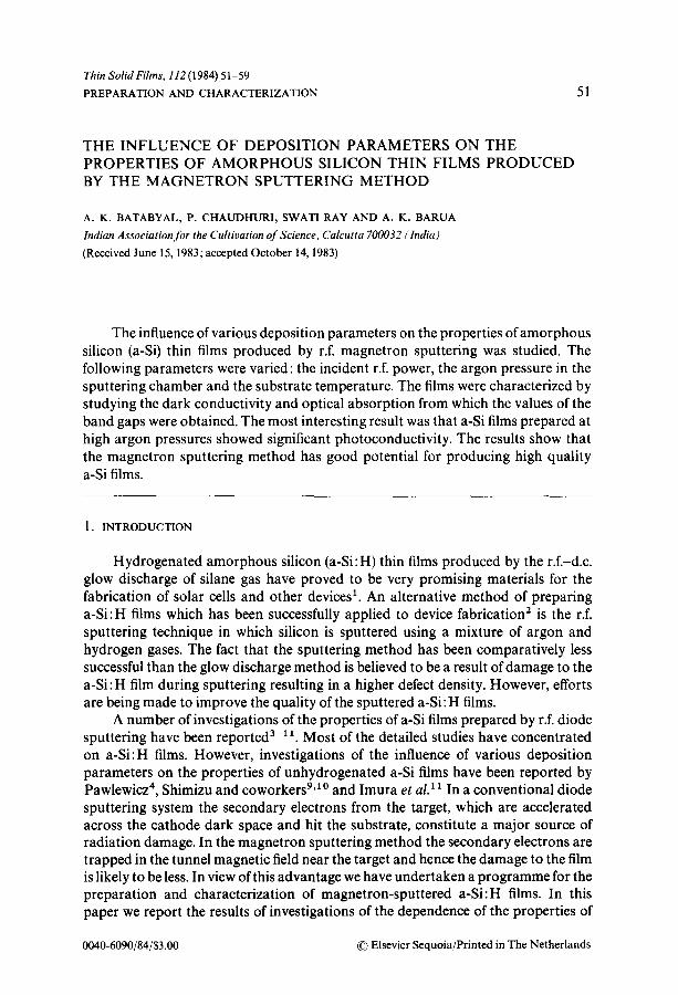
3.1. Electrical properties The effect of varying the r.f. power on the dark conductivity ~rO of a-Si films is
shown in Fig. 1. The films were deposited at 230 'C and an argon pressure of 3 x 10- 3 Torr. As the r.f. power increases from 140 to 675 W, aO decreases from 1.2! to 1.28 x 10 5 f~ i cm- 1 The conductivity increases slightly with increasing r.f. power in the higher power range. In this range there is considerable scatter in the plot of In ao versus r.f. power. The initial decrease in ao with increasing r.f. power may be due to the fact that at higher power the silicon atoms arrive at the substrate with higher kinetic energy. As a consequence increased migration of the atoms along the substrate surface is possible, resulting in an improved amorphous network and a lower concentration of microvoids which reduce the density of dangling bonds. However, as the power continues to increase the damage produced by bombard-
EFFECT OF DEPOSITION PARAMETERS ON PROPERTIES OF a-Si FILMS 53
ment with Ar ÷ ions and neutral atoms of increasing energy begins to predominate. Therefore after attaining a minimum value a D shows a gradual increase with increasing r.f. power. As the r.f. power increases from 150 W to 1 kW the amplitude of the applied r.f. voltage, which determines the energy of the ionic species in the plasma, increases from approximately 250 V to 1.2 kV.
101
10 0
o 10-2
lO-:J
I°-4 o 10- I l I I
0 200 400 600 800 1000
POWER (WATTS)
Fig. 1. D a r k conduct iv i ty cr D at 27 °C of sput tered a-Si films (prepared at a t empera tu re of 230 °C and an a rgon pressure of 3 x 10- 3 Torr) as a function of r.f. power.
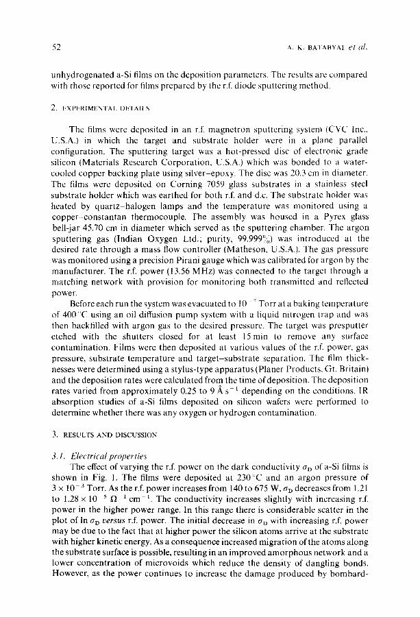
As shown in Fig. 2, In o D for the films deposited at low r.f. power (up to 480 W) is directly proportional to T-1/4. This shows that the predominant conduction mechanism for these films is hopping conduction near the Fermi level. In this case the conductivity can be written as
a D = A e x p -- (1)
The significance of the term B has been described by Mott and Davis 12. B is inversely proportional to {N(EF)} 1/4, where N(EF) is the density of states near the Fermi level. The values of B, which were obtained from the slopes of the plots of In aD versus T - 1/4, increase from 8.4 to 26.5 as the power is increased from 140 to 480 W. Thus we can infer that the density of localized states near the Fermi level decreases with increasing r.f. power within a limited range.
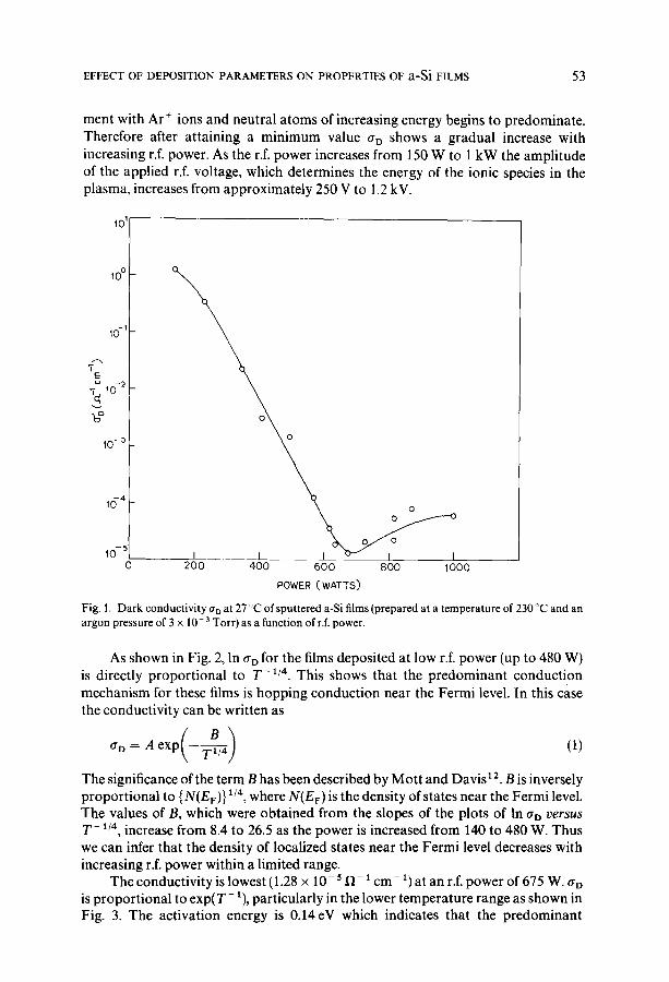
The conductivity is lowest (1.28 x 10- s f~- 1 c m - 1) at an r.f. power of 675 W. trD is proportional to exp (T- 1), particularly in the lower temperature range as shown in Fig. 3. The activation energy is 0.14eV which indicates that the predominant
54
lO 1
A. K. BATABYAL e l aL
10 c
10 - I I E o 'a
~ lo-2 o ~ _ _ 10 .3
I I tC~2.2 2.14 2.6 2.B 3.0
IO/T 4f.K-~)
Fig. 2. D a r k conduc t iv i ty an vs. IO/T ~'4 plots for a-Si films deposi ted at 230 'C and var ious r.t\ powers and a rgon pressures: curve 1, 140W, 3 x 10 -3 Torr ; curve 2, 2 3 0 W , 3 x 10 ,3 Torr ; curve 3, 340W,
3 x 10 -3 Torr ; curve 4, 480 W, 3 x 10 3 Torr ; curve 5, 235 W, 8 x 10 -3 Torr ; curve 6, 235 W, 1.5 x l0 2
Torr.
16 5
_.--,
'E Q
I0 - 7
,5 s
15 9 , , 3 4 3 ~ 1 5 6
Fig. 3. P lo ts of da rk conduc t iv i ty o" D ( ) and pho toconduc t iv i t y aeh (- - -) vs. IO3/T for a-Si films deposi ted at 230 °C and var ious r.f. powers and a rgon pressures: curve 1,675 W, 3 × 10- 3 Torr ; curves 2, 3, 230 W, 3 x 10⁻² Torr ; curves 4, 5, 230 W, 4 × 10- 2 Torr.
EFFECT OF DEPOSITION PARAMETERS ON PROPERTIES OF a-Si FILMS 55
conduction mechanism may be activated hopping near the conduction band edge. The In aD versus T - 1 plots for films deposited at high r.f. power have almost the same slope (about 0.14 eV).
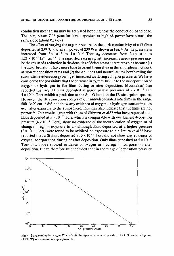
The effect of varying the argon pressure on the dark conductivity of a-Si films deposited at 230 °C and an r.f. power of 230 W is shown in Fig. 4. As the pressure is increased from 3 x 10 -3 to 4 x 10 -2 Torr o D decreases from 3.4x 10 -1 to 1.21 x 10- 7 f~- 1 c m - 1. The rapid decrease in a D with increasing argon pressure may be the result of a reduction in the densities of defect states and microvoids because (1) the adsorbed atoms have more time to orient themselves in the amorphous network at slower deposition rates and (2) the Ar ÷ ions and neutral atoms bombarding the substrate have less energy owing to increased scattering at higher pressures. We have considered the possibility that the decrease in as may be due to the incorporation of oxygen or hydrogen in the films during or after deposition. Moustakas 5 has reported that a-Si:H films deposited at argon partial pressures of 2 x 10 -2 and 4 x 10- 2 Torr exhibit a peak due to the S i - -O bond in the IR absorption spectra. However, the IR absorption spectra of our unhydrogenated a-Si films in the range 600-3400 c m - 1 did not show any evidence of oxygen or hydrogen contamination even after exposure to the atmosphere. This may also indicate that the films are not porous 13. Our results agree with those of Shimizu et al. 1° who have reported that films deposited at 5 x 10⁻² Torr, which is comparable with our highest deposition pressure (4 x 10⁻² Torr), show no evidence of the incorporation of oxygen or of changes in aD on exposure to air although films deposited at a higher pressure (2 x 10 -1 Torr) were found to be oxidized on exposure to air. Imura et al. 11 have reported that a-Si films deposited at 3 x 10 -2 Torr did not show any evidence of oxygen incorporation during or after deposition. Only films deposited at 5 x 10⁻² Torr and above showed evidence of oxygen or hydrogen incorporation after deposition. It can therefore be concluded that in the range of deposition pressure
10 - I
i ( ) 2
io -3
-y
~ 16 4
1C~ s
1() 6
10-: 10 15 20 25 30 35 40 Ar pressure (retort)
Fig. 4. Dark conductivity a o at 27 °C of a-Si films (prepared at a temperature of 230 °C and an r.f. power
of 230 W) as a function of argon pressure.
5 6 A . K . BATABYAL e[ a/.
investigated here (3 x 10 3 - 4 x 10 2 Torr) the decrease in ~-D with increasing pressure is due to the lower density of dangling bonds at higher pressures. A similar conclusion was drawn by Shimizu et al.10
It is interesting to compare the values of ao for the a-Si films investigated here with those reported by other workers for diode-sputtered films. Anderson and Paul ~ obtained ao ~ 10 -3 ~ 1 c m - 1 at an argon pressure of 5 x 10 3 T o m whereas the magne t ron sputtering method yields 6 a - - 10 2 ~ ~ cm 1 at the corresponding pressure (Fig. 4). Pawlewicz 4 obtained aD values of 10 3 ~ ~ cm 1 and 3 x l0 ~
l c m - ~ a t 2 . 5 x l 0 2 T o r r a n d l . 5 x l 0 ~Torrrespectively. The % values in this work are 2 × 1 0 5 Q ~cm I and 1 .5×10 " f~ ~cm ~ at argon pressures of 2.5 x 10 _2 Torr and 4 x 10 2 Torr respectively. Shimizu et al. 1° obtained a 60 value o f 3 . 1 6 x l 0 3 ~ ~cm l at an argon pressure of 5 x l0 2Torr . it can thus be seen that, except at low argon pressures (5 x 10 3 Torr or less), the OD values of the magnetron-sput tered films are lower than those obtained for the r.f. diode-sputtered films. The dark conductivi ty at pressures higher than 4 x 10 2 Tor t could not be investigated owing to excessive heating of the target at high plasma densities and diffusion of the plasma beyond the target area.
The In aa versus T - ~/'~ plots of a-Si films prepared at various argon pressures with conductivities of 1.3 x 10- 3 ~ - 1 cm 1 and above (Fig. 2) are linear and exhibit a gradual increase in the slope with pressure. The B values obtained from these plots increase from 26.5 to 53.4 as the pressure increases from 3 x 10 3 to 1.5 × 10 2 Torr, confirming that the density of localized states decreases with increasing pressure. It is very interesting to note that a-Si films deposited at pressures of 3 x 10 2 and 4 x 10- 2 Tor t exhibit significant photoconduct iv i ty which implies that the density of the localized recombinat ion centres is low. A photoconduct ive gain oph/r~ o of about 10 was observed under white light radiation of intensity 20 m W cm 2. The dark conductivi ty aa and the photoconduct iv i ty ap, of these two films are plotted as a function of 1 / T in Fig. 3. The plot for the film prepared at 3 x I 0 2 Torr shows two distinct linear portions. The low temperature port ion has a slope of0.13 eV while the high temperature port ion has a slope of 0.56 eV. These results suggest that hopping-
10-2!
o
~ I 0 -4
i0 -5
f ~
\ ,6o 260 2%o 3oo' - -
T s ('C)
Fig. 5. D a r k c o n d u c t i v i t y a o at 27 ~C o f a - S i films as a func t ion of the subs t r a t e l empe ra tu r e ,
EFFECT OF DEPOSITION PARAMETERS ON PROPERTIES OF a-Si FILMS 57
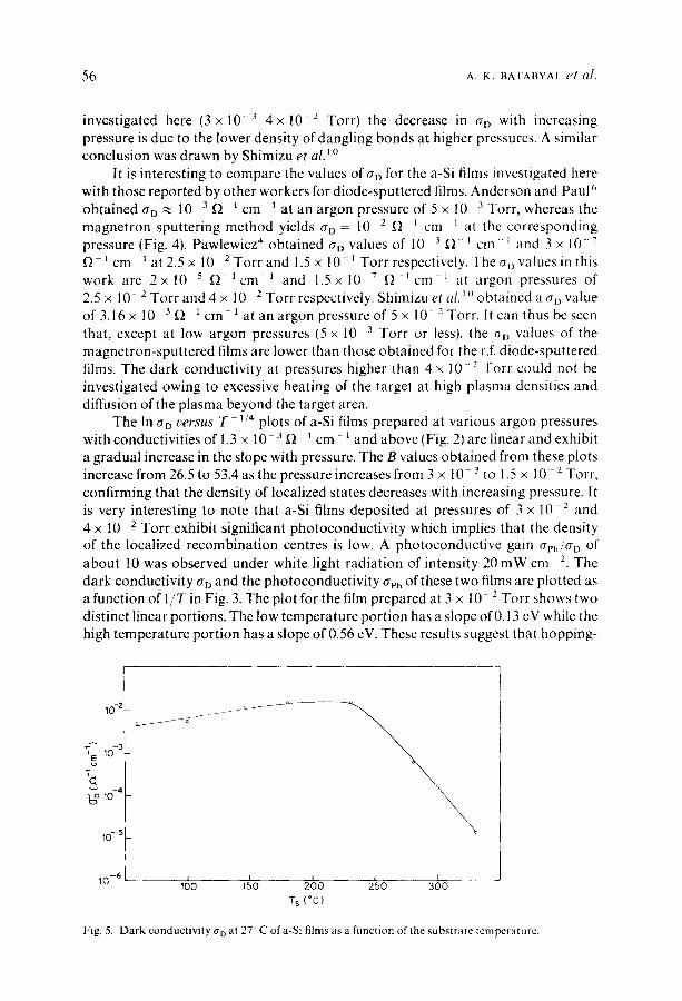
type conduction is predominant in the low temperature region and that extended state conduction is predominant in the high temperature region. The conductivity of the sample deposited at 4 x 10- 2 Torr is lowest at 27 °C (1.21 x 10- 7 f~- ~ cm- x) and yields a straight line with a single slope of 0.62 eV when plotted as In aD against T - ~. This result implies extended state conduction. Shimizu e t al. 9 also reported a gradual increase in the activation energy with increasing pressure for films deposited in the pressure range 5 × 10- 2-3 × 10- ~ Torr with a value of about 0.9 eV for the highest pressure.
The variation in ao with the substrate temperature was also studied and the results are shown in Fig. 5. In the lower substrate temperature range up to 240 °C the conductivity is almost independent of temperature. However, at higher tempera- tures the conductivity decreases rapidly with increasing substrate temperature. This may be due to the formation of an improved amorphous network as a result of high mobility or increased migration of atoms on the surface at higher temperatures. There may also be some annealing of the microvoids. All these factors result in a decrease in the density of the dangling bonds ~4.
to 6
,J r---I
10 4
1 0 2 /
I'0 I I 1
1'5 2"0 2"5
A ~' (e v)
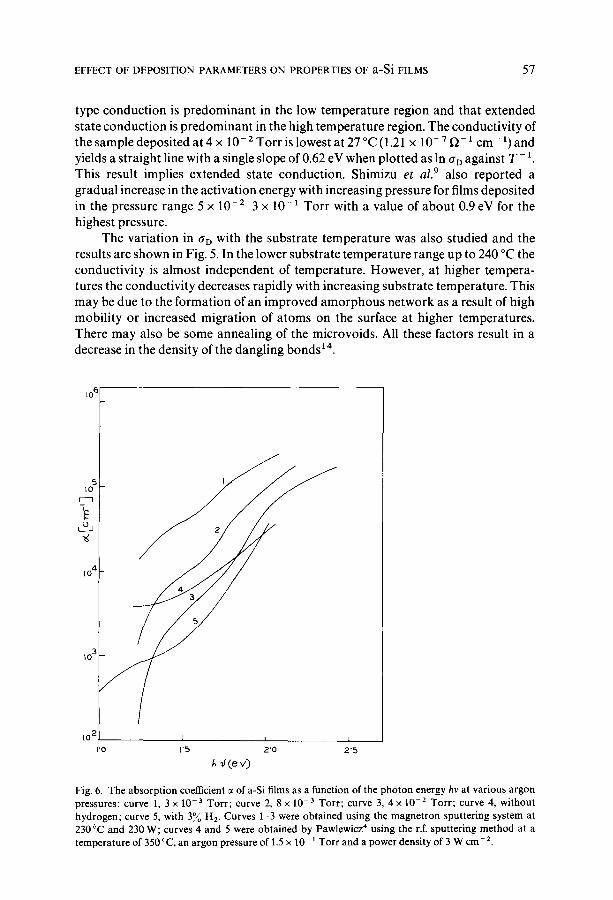
Fig. 6. The absorption coefficient ~ of a-Si films as a function of the photon energy hv at various argon pressures: curve 1, 3 x 10 -3 Torr; curve 2, 8 × 10 -3 Torr; curve 3, 4 x 10 -2 Torr; curve 4, without
hydrogen; curve 5, with 3~ H 2. Curves 1-3 were obtained using the magnetron sputtering system at 230 'C and 230 W; curves 4 and 5 were obtained by Pawlewicz 4 using the r.f. sputtering method at a temperature of 350 °C, an argon pressure of 1.5 x 10⁻¹ Torr and a power density of 3 W cm- 2.
58 A .K . BATABYAL el al.
10001
5OO
.~ 400
30C
/ / /
,/ /
,/ 2
/ / / ./ i /
//
i/I ii /
J 100 z j, / //
/¢ // // ,;
.0. 15 2.0 2.5 ha? (eV)
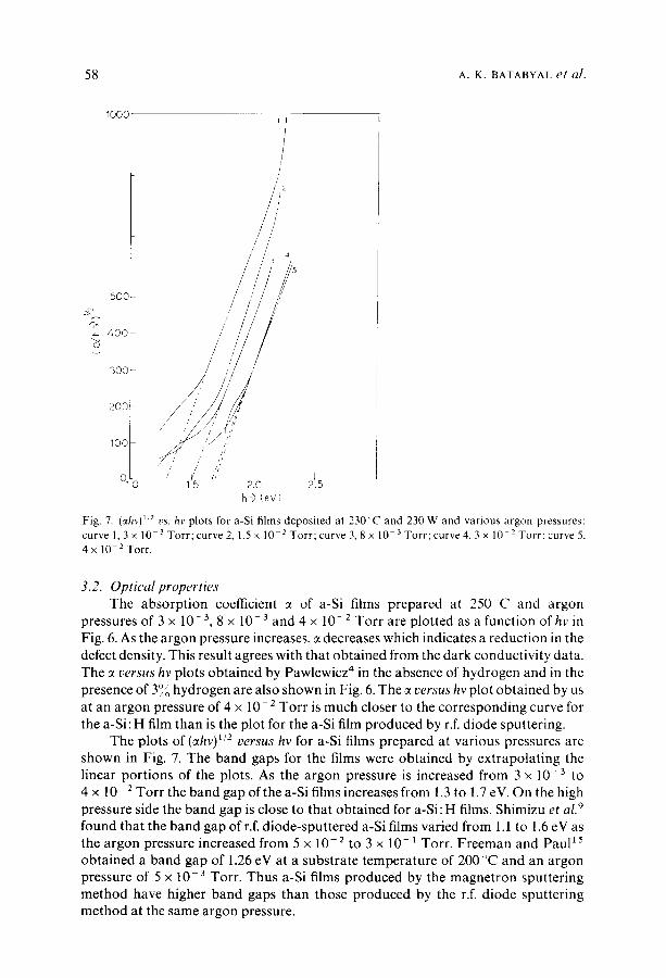
]Fig. 7. (~hv) 1¢2 vs. hv plots for a-Si films deposited at 230'C and 230 W and various argon pressures: curvel, 3 x l 0 3Torr ;curve2,1.5x l0 2Tor r ;curve3,8x l0 3Tor r ;curve4,3x l0 2Tort:curve5. 4 x 10- 2 Tort.
3.2. Opt ical propert ies
The absorpt ion coefficient :t of a-Si films prepared at 2 5 0 C and argon pressures of 3 x 10- 3, 8 x 10- 3 and 4 x 10- z Torr are plotted as a function of hv in Fig. 6. As the argon pressure increases, ~ decreases which indicates a reduction in the defect density. This result agrees with that obtained from the dark conductivi ty data. The ct versus hv plots obtained by Pawlewicz 4 in the absence of hydrogen and in the presence of 3% hydrogen are also shown in Fig. 6. The ~ versus hv plot obtained by us at an argon pressure of 4 x 10- 2 Tor t is much closer to the corresponding curve for the a-Si: H film than is the plot for the a-Si film produced by r.f. diode sputtering.
The plots of (o~hv) 1/2 versus hv for a-Si films prepared at various pressures are shown in Fig. 7. The band gaps for the films were obtained by extrapolat ing the linear port ions of the plots. As the argon pressure is increased from 3 x 10- 3 to 4 x 10 2 Torr the band gap of the a-Si films increases from 1.3 to 1.7 eV. On the high pressure side the band gap is close to that obtained for a -Si :H films. Shimizu et al. 9
found that the band gap of r.f. diode-sputtered a-Si films varied from !.1 to 1.6 eV as the argon pressure increased from 5 x 10 2 to 3 x 10 t Torr. Freeman and Paul is obtained a band gap of 1.26 eV at a substrate temperature of 200 °C and an argon pressure of 5 x 10⁻³ Torr. Thus a-Si films produced by the magne t ron sputtering method have higher band gaps than those produced by the r.f. diode sputtering method at the same argon pressure.
EFFECT OF DEPOSITION PARAMETERS ON PROPERTIES OF a-Si FILMS 59
4. CONCLUSIONS
Studies of the influence of various deposi t ion parameters on a-Si films prepared by the magne t ron sputter ing technique show the potential of this technique for producing good quali ty a-Si films. Fur ther studies, part icularly of a -Si :H films prepared by this technique, are therefore necessary.
ACKNOWLEDGMENT
The authors are grateful to the Depar tment of Science and Technology,
G o v e r n m e n t of India, for funding the project.
REFERENCES
1 D. Carlson, Sol. Energy Mater., 3 (1980) 106. 2 T.D. Moustakas and R. Friedman, Appl. Phys. Lett., 40 (1982) 515. 3 W. Paul and D. A. Anderson, Sol. Energy Mater., 5 (1981) 229. 4 W.T. Pawlewicz, J. Appl. Phys., 49 (1978) 5595. 5 T.D. Moustakas, Sol. Energy Mater., 8 (1982) 187. 6 D.A. Anderson and W. Paul, Philos. Mag., 44 (1981) 187. 7 T.D. Moustakas, D. A. Anderson and W. Paul, SolidState Commun., 23 (1977) 155. 8 M.H. Brodsky, R. S. Title, K. Weiser and G. D. Pettit, Phys. Rev. B, 1 (1970) 2632. 9 T. Shimizu, M. Kumeda, J. Watanabe and K. Kamono, Jpn. J. Appl. Phys., 18 (1979) 1923.
10 T. Shimizu, N. Kumeda, I. Watanabe and Y. Kiriyama, Jpn. J. Appl. Phys., 19 (1980) L235. 11 T. Imura, K. Ushita and A. Hiraki, Jpn. J. Appl. Phys., 19 (1980) L65. 12 N.F. Mott and E. A. Davis, Electronic Processes in Non-crystalline Materials, Clarendon, Oxford,
1979, p. 34. 13 D.K. Biegelsen, R. A. Street, C. C. Tsai and J. C. Knights, Phys. Rev. B, 20 (1979) 4839. 14 W. Paul, G. A. N. Connell and R. J. Temkin, Adv. Phys., 22 (1973) 529. 15 E.C. Freeman and W. Paul, Phys. Rev. B, 20 (1979) 716.

Related Documents


![[PPT]Home-Made DC Magnetron Sputtering System - …faculty.kfupm.edu.sa/.../research_files/magnetron.ppt · Web viewHome-Made DC Magnetron Sputtering System Chamber and Gas supply](https://static.cupdf.com/doc/110x72/5aa9b1b37f8b9a90188d2f45/ppthome-made-dc-magnetron-sputtering-system-viewhome-made-dc-magnetron-sputtering.jpg)


