Elsevier Science 1 1 1 The IceCube Data Acquisition System: Signal Capture, 2 Digitization, and Timestamping 3 R. Abbasi t , M. Ackermann af , J. Adams k , M. Ahlers y , J. Ahrens u , K. Andeen t , J. Auffenberg ae , X. Bai w , M. 4 Baker t , S. W. Barwick p , R. Bay e , J. L. Bazo Alba af , K. Beattie f , T. Becka u , J. K. Becker m , K.-H. Becker ae , P. 5 Berghaus t , D. Berley l , E. Bernardini af , D. Bertrand h , D. Z. Besson r , B. Bingham f , E. Blaufuss l , D. J. 6 Boersma t , C. Bohm z , J. Bolmont af , S. Böser af , O. Botner ac , J. Braun t , D. Breeder ae , T. Burgess z , W. Carithers 7 f , T. Castermans v , H. Chen f , D. Chirkin t , B. Christy l , J. Clem w , D. F. Cowen ab,aa , M. V. D'Agostino e , M. 8 Danninger k , A. Davour ac , C. T. Day f , O. Depaepe i , C. De Clercq i , L. Demirörs q , F. Descamps n , P. Desiati t , G. 9 de Vries-Uiterweerd n , T. DeYoung ab , J. C. Diaz-Velez t , J. Dreyer m , J. P. Dumm t , M. R. Duvoort ad , W. R. 10 Edwards f , R. Ehrlich l , J. Eisch t , R. W. Ellsworth l , O. Engdegård ac , S. Euler a , P. A. Evenson w , O. Fadiran c , A. 11 R. Fazely d , T. Feusels n , K. Filimonov e , C. Finley t , M. M. Foerster ab , B. D. Fox ab , A. Franckowiak g , R. Franke 12 af , T. K. Gaisser w , J. Gallagher s , R. Ganugapati t , L. Gerhardt f , L. Gladstone t , D. Glowacki t , A. Goldschmidt f , 13 J. A. Goodman l , R. Gozzini u , D. Grant ab , T. Griesel u , A. Groß o,k , S. Grullon t , R. M. Gunasingha d , M. Gurtner 14 ae , C. Ha ab , A. Hallgren ac , F. Halzen t , K. Han k , K. Hanson t , R. Hardtke y , Y. Hasegawa j , J. Haugen t , D. Hays f , 15 J. Heise ad , K. Helbing ae , M. Hellwig u , P. Herquet v , S. Hickford k , G. C. Hill t , J. Hodges t , K. D. Hoffman l , K. 16 Hoshina t , D. Hubert i , W. Huelsnitz l , B. Hughey t , J.-P. Hülß a , P. O. Hulth z , K. Hultqvist z , S. Hussain w , R. L. 17 Imlay d , M. Inaba j , A. Ishihara j , J. Jacobsen t , G. S. Japaridze c , H. Johansson z , A. Jones f , J. M. Joseph f , K.-H. 18 Kampert ae , A. Kappes t,1 , T. Karg ae , A. Karle t , H. Kawai j , J. L. Kelley t , J. Kiryluk f,e , F. Kislat af , S. R. Klein f,e , 19 S. Kleinfelder f , S. Klepser af , G. Kohnen v , H. Kolanoski g , L. Köpke u , M. Kowalski g , T. Kowarik u , M. 20 Krasberg t , K. Kuehn p , E. Kujawski f , T. Kuwabara w , M. Labare h , K. Laihem a , H. Landsman t , R. Lauer af , A. 21 Laundrie t , H. Leich af , D. Leier m , C. Lewis t , A. Lucke g , J. Ludvig f , J. Lundberg ac , J. Lünemann m , J. Madsen y , 22 R. Maruyama t , K. Mase j , H. S. Matis f,2 , C. P. McParland f , K. Meagher l , A. Meli m , M. Merck t , T. Messarius m , 23 P. Mészáros ab,aa , R. H. Minor f , H. Miyamoto j , A. Mohr g , A. Mokhtarani f , T. Montaruli t,3 , R. Morse t , S. M. 24 1 On leave of absence from Universität Erlangen-Nürnberg, Physikalisches Institut, D-91058, Erlangen, Germany. 2 Corresponding author. Tel.: +1-510-486-5031; fax: +1-510-486-4818; e-mail: [email protected]. 3 On leave of absence from Università di Bari and INFN, Dipartimento di Fisica, I-70126, Bari, Italy. Manuscript

Welcome message from author
This document is posted to help you gain knowledge. Please leave a comment to let me know what you think about it! Share it to your friends and learn new things together.
Transcript
Elsevier Science 1
1
1
The IceCube Data Acquisition System: Signal Capture, 2
Digitization, and Timestamping3
R. Abbasi t, M. Ackermann af, J. Adams k, M. Ahlers y, J. Ahrens u, K. Andeen t, J. Auffenberg ae, X. Bai w, M. 4
Baker t, S. W. Barwick p, R. Bay e, J. L. Bazo Alba af, K. Beattie f, T. Becka u, J. K. Becker m, K.-H. Becker ae, P. 5
Berghaus t, D. Berley l, E. Bernardini af, D. Bertrand h, D. Z. Besson r, B. Bingham f, E. Blaufuss l, D. J. 6
Boersma t, C. Bohm z, J. Bolmont af, S. Böser af, O. Botner ac, J. Braun t, D. Breeder ae, T. Burgess z, W. Carithers 7f, T. Castermans v, H. Chen f, D. Chirkin t, B. Christy l, J. Clem w, D. F. Cowen ab,aa, M. V. D'Agostino e, M. 8
Danninger k, A. Davour ac, C. T. Day f, O. Depaepe i, C. De Clercq i, L. Demirörs q, F. Descamps n, P. Desiati t, G. 9
de Vries-Uiterweerd n, T. DeYoung ab, J. C. Diaz-Velez t, J. Dreyer m, J. P. Dumm t, M. R. Duvoort ad, W. R. 10
Edwards f, R. Ehrlich l, J. Eisch t, R. W. Ellsworth l, O. Engdegård ac, S. Euler a, P. A. Evenson w, O. Fadiran c, A. 11
R. Fazely d, T. Feusels n, K. Filimonov e, C. Finley t, M. M. Foerster ab, B. D. Fox ab, A. Franckowiak g, R. Franke 12af, T. K. Gaisser w, J. Gallagher s, R. Ganugapati t, L. Gerhardt f, L. Gladstone t, D. Glowacki t, A. Goldschmidt f, 13
J. A. Goodman l, R. Gozzini u, D. Grant ab, T. Griesel u, A. Groß o,k, S. Grullon t, R. M. Gunasingha d, M. Gurtner 14ae, C. Ha ab, A. Hallgren ac, F. Halzen t, K. Han k, K. Hanson t, R. Hardtke y, Y. Hasegawa j, J. Haugen t, D. Hays f, 15
J. Heise ad, K. Helbing ae, M. Hellwig u, P. Herquet v, S. Hickford k, G. C. Hill t, J. Hodges t, K. D. Hoffman l, K. 16
Hoshina t, D. Hubert i, W. Huelsnitz l, B. Hughey t, J.-P. Hülß a, P. O. Hulth z, K. Hultqvist z, S. Hussain w, R. L. 17
Imlay d, M. Inaba j, A. Ishihara j, J. Jacobsen t, G. S. Japaridze c, H. Johansson z, A. Jones f, J. M. Joseph f, K.-H. 18
Kampert ae, A. Kappes t,1, T. Karg ae, A. Karle t, H. Kawai j, J. L. Kelley t, J. Kiryluk f,e, F. Kislat af, S. R. Klein f,e, 19
S. Kleinfelder f, S. Klepser af, G. Kohnen v, H. Kolanoski g, L. Köpke u, M. Kowalski g, T. Kowarik u, M. 20
Krasberg t, K. Kuehn p, E. Kujawski f, T. Kuwabara w, M. Labare h, K. Laihem a, H. Landsman t, R. Lauer af, A. 21
Laundrie t, H. Leich af, D. Leier m, C. Lewis t, A. Lucke g, J. Ludvig f, J. Lundberg ac, J. Lünemann m, J. Madsen y, 22
R. Maruyama t, K. Mase j, H. S. Matis f,2, C. P. McParland f, K. Meagher l, A. Meli m, M. Merck t, T. Messarius m, 23
P. Mészáros ab,aa, R. H. Minor f, H. Miyamoto j , A. Mohr g, A. Mokhtarani f , T. Montaruli t,3, R. Morse t, S. M. 24
1 On leave of absence from Universität Erlangen-Nürnberg, Physikalisches Institut, D-91058, Erlangen, Germany.2
Corresponding author. Tel.: +1-510-486-5031; fax: +1-510-486-4818; e-mail: [email protected] On leave of absence from Università di Bari and INFN, Dipartimento di Fisica, I-70126, Bari, Italy.
Manuscript
Elsevier Science2
2
Movit aa, K. Münich m, A. Muratas f, R. Nahnhauer af, J. W. Nam p, P. Nießen w, D. R. Nygren f, S. Odrowski o, A. 25
Olivas l, M. Olivo ac, M. Ono j, S. Panknin g, S. Patton f, C. Pérez de los Heros ac, J. Petrovic h, A. Piegsa u, D. 26
Pieloth af, A. C. Pohl ac,4, R. Porrata e, N. Potthoff ae, J. Pretz l, P. B. Price e, G. T. Przybylski f, K. Rawlins b, S. 27
Razzaque ab,aa, P. Redl l, E. Resconi o, W. Rhode m, M. Ribordy q, A. Rizzo i, W. J. Robbins ab, J. P. Rodrigues t, 28
P. Roth l, F. Rothmaier u, C. Rott ab,5, C. Roucelle f.e, D. Rutledge ab, D. Ryckbosch n, H.-G. Sander u, S. Sarkar x, 29
K. Satalecka af, P. Sandstrom t, S. Schlenstedt af, T. Schmidt l, D. Schneider t, O. Schulz o, D. Seckel w, B. 30
Semburg ae, S. H. Seo z, Y. Sestayo o, S. Seunarine k, A. Silvestri p, A. J. Smith l, C. Song t, J. E. Sopher f, G. M. 31
Spiczak y, C. Spiering af, T. Stanev w, T. Stezelberger f, R. G. Stokstad f, M. C. Stoufer f, S. Stoyanov w, E. A. 32
Strahler t, T. Straszheim l, K.-H. Sulanke af, G. W. Sullivan l, Q. Swillens h, I. Taboada e,6, O. Tarasova af, A. Tepe 33ae, S. Ter-Antonyan d, S. Tilav w, M. Tluczykont af, P. A. Toale ab, D. Tosi af, D. Turčan l, N. van Eijndhoven ad, J. 34
Vandenbroucke e, A. Van Overloop n, V. Viscomi ab, C. Vogt a, B. Voigt af, C. Q. Vu f, D. Wahl t, C. Walck z, T. 35
Waldenmaier w, H. Waldmann af, M. Walter af, C. Wendt t, S. Westerhof t, N. Whitehorn t, D. Wharton t, C. H. 36
Wiebusch a, C. Wiedemann z, G. Wikström z, D. R. Williams ab,7, R. Wischnewski af, H. Wissing a, K. Woschnagg 37e, X. W. Xu d, G. Yodh p, S. Yoshida j38
(The IceCube Collaboration)39
aIII Physikalisches Institut, RWTH Aachen University, D-52056 Aachen, Germany40
bDept. of Physics and Astronomy, University of Alaska Anchorage, 3211 Providence Dr., Anchorage, AK 99508, USA41
cCTSPS, Clark-Atlanta University, Atlanta, GA 30314, USA42
dDept. of Physics, Southern University, Baton Rouge, LA 70813, USA43
eDept. of Physics, University of California, Berkeley, CA 94720, USA44
fLawrence Berkeley National Laboratory, Berkeley, CA 94720, USA45
g Institut für Physik, Humboldt-Universität zu Berlin, D-12489 Berlin, Germany46
hUniversité Libre de Bruxelles, Science Faculty CP230, B-1050 Brussels, Belgium47
iVrije Universiteit Brussel, Dienst ELEM, B-1050 Brussels, Belgium48j
Dept. of Physics, Chiba University, Chiba 263-8522, Japan49k
Dept. of Physics and Astronomy, University of Canterbury, Private Bag 4800, Christchurch, New Zealand50l
Dept. of Physics, University of Maryland, College Park, MD 20742, USA51m
Dept. of Physics, Universität Dortmund, D-44221 Dortmund, Germany52 4 Affiliated with School of Pure and Applied Natural Sciences, Kalmar University, S-39182 Kalmar, Sweden.5 Currently at Dept. of Physics and Center for Cosmology and Astro-Particle Physics, The Ohio State University, Columbus, OH 43210,
USA.6
Currently at the School of Physics and Center for Relativistic Astrophysics, Georgia Institute of Technology, Atlanta, GA 30332, USA.7
Currently at the Dept. of Physics and Astronomy, University of Alabama, Tuscaloosa, AL 35487, USA.
Elsevier Science 3
3
n
Dept. of Subatomic and Radiation Physics, University of Gent, B-9000 Gent, Belgium53o
Max-Planck-Institut für Kernphysik, D-69177 Heidelberg, Germany54p
Dept. of Physics and Astronomy, University of California, Irvine, CA 92697, USA55qLaboratory for High Energy Physics, École Polytechnique Fédérale, CH-1015 Lausanne, Switzerland56
r
Dept. of Physics and Astronomy, University of Kansas, Lawrence, KS 66045, USA57s
Dept. of Astronomy, University of Wisconsin, Madison, WI 53706, USA58t
Dept. of Physics, University of Wisconsin, Madison, WI 53706, USA59u
Institute of Physics, University of Mainz, Staudinger Weg 7, D-55099 Mainz, Germany60v
University of Mons-Hainaut, 7000 Mons, Belgium61w
Bartol Research Institute, University of Delaware, Newark, DE 19716, USA62x
Dept. of Physics, University of Oxford, 1 Keble Road, Oxford OX1 3NP, UK63y
Dept. of Physics, University of Wisconsin, River Falls, WI 54022, USA64z
Dept. of Physics, Stockholm University, SE-10691 Stockholm, Sweden65aa
Dept. of Astronomy and Astrophysics, Pennsylvania State University, University Park, PA 16802, USA66ab
Dept. of Physics, Pennsylvania State University, University Park, PA 16802, USA67ac
Division of High Energy Physics, Uppsala University, S-75121 Uppsala, Sweden68ad
Dept. of Physics and Astronomy, Utrecht University/SRON, NL-3584 CC Utrecht, The Netherlands69ae
Dept. of Physics, University of Wuppertal, D-42119 Wuppertal, Germany70af
DESY, D-15735 Zeuthen, Germany71
Elsevier use only: Received date here; revised date here; accepted date here72
Abstract73
IceCube is a km-scale neutrino observatory under construction at the South Pole with sensors both in the deep ice 74(InIce) and on the surface (IceTop). The sensors, called Digital Optical Modules (DOMs), detect, digitize and 75timestamp the signals from optical Cherenkov-radiation photons. The DOM Main Board (MB) data acquisition 76subsystem is connected to the central DAQ in the IceCube Laboratory (ICL) by a single twisted copper wire-pair 77and transmits packetized data on demand. Time calibration is maintained throughout the array by regular 78transmission to the DOMs of precisely timed analog signals, synchronized to a central GPS-disciplined clock. 79The design goals and consequent features, functional capabilities, and initial performance of the DOM MB, and 80the operation of a combined array of DOMs as a system, are described here. Experience with the first InIce 81strings and the IceTop stations indicates that the system design and performance goals have been achieved.82

Elsevier Science4
4
PACS: 95.55.Vj; 95.85.Ry, 29.40.Ka, 29.40.Gx84
Keywords: Neutrino Telescope, IceCube, signal digitization. AMANDA85
Elsevier Science 5
5
1. IceCube Overview86
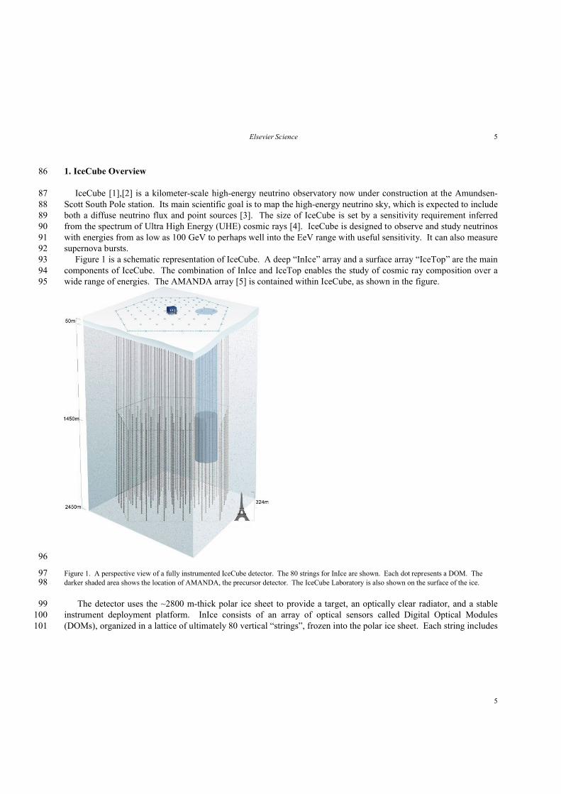
IceCube [1],[2] is a kilometer-scale high-energy neutrino observatory now under construction at the Amundsen-87Scott South Pole station. Its main scientific goal is to map the high-energy neutrino sky, which is expected to include 88both a diffuse neutrino flux and point sources [3]. The size of IceCube is set by a sensitivity requirement inferred 89from the spectrum of Ultra High Energy (UHE) cosmic rays [4]. IceCube is designed to observe and study neutrinos 90with energies from as low as 100 GeV to perhaps well into the EeV range with useful sensitivity. It can also measure 91supernova bursts.92
Figure 1 is a schematic representation of IceCube. A deep “InIce” array and a surface array “IceTop” are the main 93components of IceCube. The combination of InIce and IceTop enables the study of cosmic ray composition over a 94wide range of energies. The AMANDA array [5] is contained within IceCube, as shown in the figure.95
96
Figure 1. A perspective view of a fully instrumented IceCube detector. The 80 strings for InIce are shown. Each dot represents a DOM. The 97darker shaded area shows the location of AMANDA, the precursor detector. The IceCube Laboratory is also shown on the surface of the ice.98
The detector uses the ~2800 m-thick polar ice sheet to provide a target, an optically clear radiator, and a stable 99instrument deployment platform. InIce consists of an array of optical sensors called Digital Optical Modules 100(DOMs), organized in a lattice of ultimately 80 vertical “strings”, frozen into the polar ice sheet. Each string includes 101
Elsevier Science6
6
60 DOMs, spaced uniformly from a depth of 1450 to 2450 m. There are plans to create a densely instrumented deep 102core in the center of IceCube by adding six special strings with more closely spaced optical modules concentrated in 103the clearest ice toward the bottom [6].104
A string is deployed into a water-filled hole, which has been bored with a hot-water jet. Once the water refreezes, 105the DOMs become permanently inaccessible. Heat flow from within the earth introduces a vertical thermal gradient 106in the ice, leading to a variation in the internal operating temperature of the DOMs from -9C at the lowest elevation 107DOM to -32C at the uppermost DOM.108
The IceTop surface air shower array consists of pairs of tanks placed about 25 meters from the top of each down-109hole cable and separated from each other by 10 meters. Each tank is instrumented with two DOMs frozen into the 110top of the ice in the tanks. The DOMs capture Cherenkov light generated by charged particles passing through the 111tanks. Typical signals are much bigger than signals in the deep ice. For example, a single muon typically generates a 112signal with a total charge equivalent to 130 photoelectrons, and a large air shower often produces a signal equivalent 113to tens or hundreds of muons. Operating temperatures for IceTop stations vary seasonally from -40C to -20C. The 114ice temperature is about 10C lower than the board temperature.115
A DOM contains a photomultiplier tube (PMT), which detects the blue and near-UV Cherenkov light produced by 116relativistic charged particles passing through the ice. Photons travel long distances due to the large absorption length 117of well above 100 m on average. Scattering in the ice disperses photon arrival times and directions for distances that 118are large compared to the effective scattering length of ~24 m. The signal shape depends on both the distance from 119the source and its linear extent. The width in time generally increases with the track’s distance from the DOM. In 120addition, the reconstruction of InIce cascades and IceTop air showers places further requirements on the DAQ 121architecture. The very wide range of possible energy depositions leads to a demanding requirement on dynamic 122range in the detectors. Digital information from the ensemble of DOMs allows reconstruction of event topology and 123energy, from which the nature of the event may be determined. 124
In this paper, we concentrate on system aspects of hardware and software elements of IceCube that capture and 125process the primary signal information. We discuss hardware design and implementation, and demonstrate 126functionality. The clock distribution scheme used by IceCube is novel, and so we early on focused on our ability to 127do time calibration. Results from that effort are included. Our ability to calibrate the trigger efficiency and the 128waveform digitizers for charge and feature extraction will be presented in a later paper.129
Sections 2-4 provide conceptual overviews, performance goals, and basic technical aspects. Section 5 describes 130manufacturing and testing procedures, while Section 6 summarizes the performance and reliability up to August 1312008.132
2. DAQ - Technical Design133
In the broadest sense, the primary goal for the IceCube DAQ is to capture and timestamp with high accuracy, the 134complex, widely varying optical signals over the maximum dynamic range provided by the PMT. To meet this goal, 135the IceCube DAQ architecture is decentralized. The digitization is done individually inside each DOM, and then 136collected in the counting house in the IceCube Laboratory (ICL), which is located on the surface of the ice. 137
Operationally, the DOMs in IceCube resemble an ensemble of satellites, with interconnects and communication 138via copper wire-pairs. The data collection process is centrally managed over this digital communications and time 139signal distribution network. Power is also distributed over this network. This decentralized approach places complex 140
Elsevier Science 7
7
electronic subsystems beyond any possibility of access for maintenance. Hence, reliability and programmability 141considerations were drivers in the engineering process.142
The goal of this architecture is to obtain very high information quality with minimal on-site personnel needed at 143the South Pole during both detector commissioning and operation. The IceCube DAQ design relies upon the 144collaboration’s understanding of how to build a digital system after studying from the behavior 41 prototype DOMs 145[8] deployed in AMANDA.146
2.1. The “Hit” – The Fundamental IceCube Datum147
The primary function of the DOM is to produce a digital output record, called a “Hit” whenever one or more 148photons are detected. The basic elements of a Hit are a timestamp generated locally within the DOM and waveform 149information. A Hit can range in size from a minimum of 12 bytes to several hundred bytes depending on the 150waveform's complexity and trigger conditions. A Hit always contains at least a timestamp, a coarse measure of 151charge, and several bits defining Hit origin.152
Waveform information is collected for a programmable interval – presently chosen to be 6.4 s, which is more 153than the maximum time interval over which the most energetic events are expected to contribute detectable light to 154any one DOM. 155
Hardware trigger signals exchanged between neighboring channels may be utilized by the DOM trigger logic to 156limit data flow by either minimizing the level of waveform detail within a Hit, or by rejecting Hits that are isolated –157i.e., with no nearby Hits in time or space, and hence much more likely to be PMT noise than real physics events. 158
2.2. DAQ Elements Involved in Generating Hits159
The real-time IceCube DAQ includes those functional blocks of IceCube that contribute to time-calibrated Hits:1601. The Digital Optical Module, deployed in both InIce and IceTop.1612. The DOMHub, located in the ICL, and based on an industrial PC.1623. The Cable Network, which connects DOMs to the DOMHub and adjacent DOMs to each other.1634. The Master Clock, which distributes time calibration (RAPcal) signals derived from a GPS receiver to the 164
DOMHubs.1655. The Stringhub, a software element that, among other tasks, maps Hits from DOM clock units to the clock 166
domain of the ICL and time-orders the Hit stream for an entire string.167Together, these elements capture the PMT anode pulses above a configurable threshold with a minimum set value 168
of ~0.25 single photoelectron (SPE) pulse height, and transform the information to an ensemble of timestamped, 169time-calibrated, and time-ordered digital data blocks.170
2.3. The Digital Optical Module – Overview 171
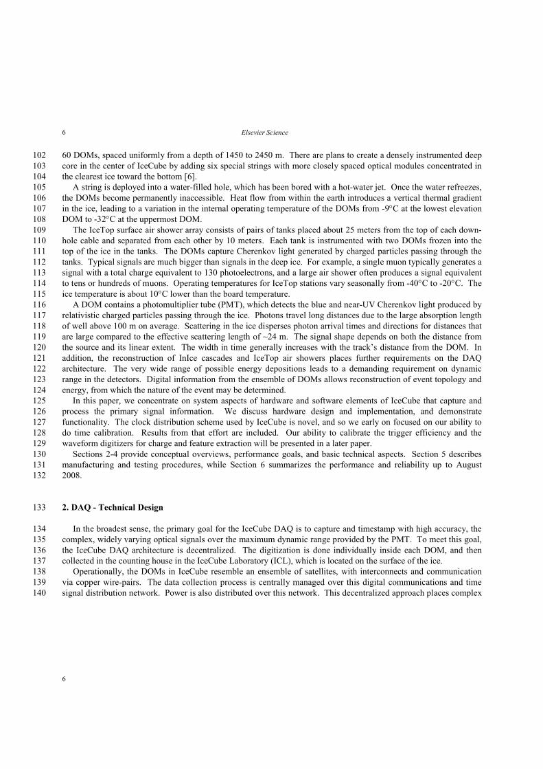
The DOM’s main elements are a 25 cm diameter PMT (Hamamatsu R7081-02), a modular 2 KV high voltage 172(HV) power supply for the PMT, a separate passive base for PMT operation, the DOM Main Board (MB), a stripline 173signal delay board, and a 13 mm thick glass sphere to withstand the pressure of its deep deployment. A flexible gel 174provides support and optical coupling from the glass sphere to the PMT’s face. Figure 2 is an illustration of a DOM 175with its components.176
The assembled DOM is filled with dry nitrogen to a pressure of approximately ½ atmosphere. This maintains a 177strong compressive force on the sphere, assuring mechanical integrity of the circumferential seal during handling, 178
Elsevier Science8
8
storage, and deployment. The DOM provides built-in electronic sensing of the gas pressure within the assembled 179DOM, enabling the detection of a fault either in the seal or failure of the PMT vacuum.180
181
Figure 2. A schematic illustration of a DOM. The DOM contains a HV generator with divides the voltage to the photomultiplier. The DOM 182Mainboard or DOM MB digitizes the signals from the phototube, actives the LEDs on the LED flasher board, and communicates with the surface. 183A mu-metal grid shields the phototube against the Earth’s magnetic field. The phototube is optically coupled to the exterior Glass Pressure 184Housing by RTV gel. The penetrator provides a path where the wires from the surface can pass through the Glass Pressure shield.185
The PMT is operated with the photocathode grounded. The anode signal formation hence occurs at positive HV. 186This analog signal is presented to the DOM MB signal path, DC-coupled from the input to a digitizer. At the input, 187the signal is split to a high-bandwidth PMT discriminator path and to a 75 ns high quality delay line, which provides 188enough time for the downstream electronics to receive a trigger from the discriminator. 189
The DOM MB (Figure 3), the “central processor” of the DOM, receives the PMT signals. After digitization, the 190DOM MB formats the data to create a Hit. High-bandwidth waveform capture is accomplished by an application191specific integrated circuit (ASIC), the Analog Transient Waveform Digitizer (ATWD) [9]. Data is buffered until the 192DOM MB receives a request to transfer data to the ICL.193
In addition to the signal capture/digitization scheme, the use of free-running high-stability oscillators in the DOMs 194is an innovation that permits the precise time calibration of data without actual synchronization, and at the same time 195creates negligible impact on network bandwidth. Timestamping of data is realized by a Reciprocal Active Pulsing 196(RAPcal) [10] procedure, which is described in Section 4.7. 197
Elsevier Science 9
9
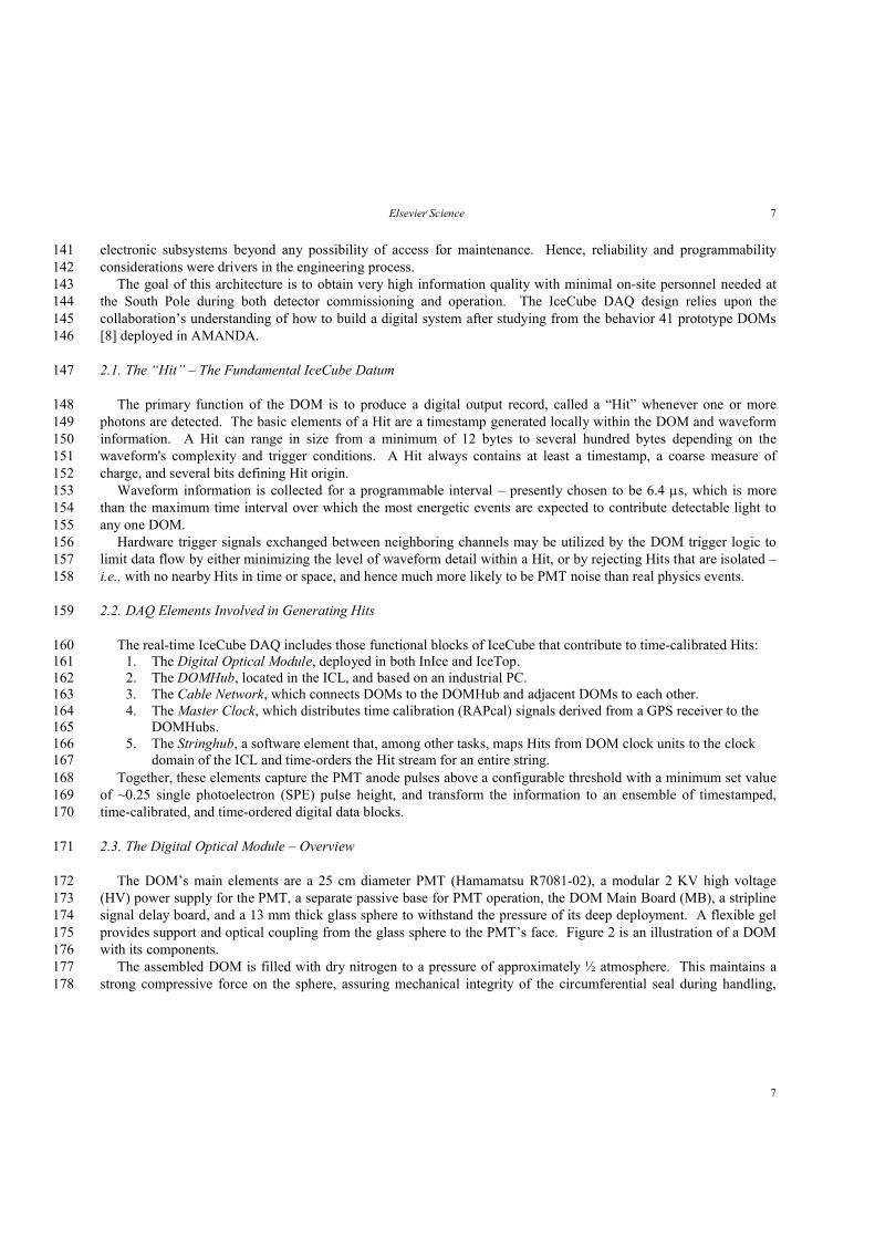
198Figure 3. A photograph of the DOM MB. The diameter of the circuit board is 274 mm. This circular circuit board communicates with the surface 199and provides power and drives the other electronics board inside the DOM. This photograph shows the location of the components, which are 200described in the text.201
The DOM includes a “flasher” board hosting 12 LEDs that can be actuated to produce bright UV optical pulses 202detectable by other DOMs. Flasher board LEDs can be pulsed either individually or in combinations at 203programmable output levels and pulse lengths. They are used to stimulate and calibrate distant DOMs, simulate 204physical events, and to investigate optical properties of the ice. In addition, the DOM MB is equipped with an “on-205board LED”, which delivers precisely timed, but weak signals for calibration of single photoelectron pulses and PMT 206transit times. A complete description of the DOM MB, including its other functions, can be found in the next section.207
2.4. DOM MB Technical Design208
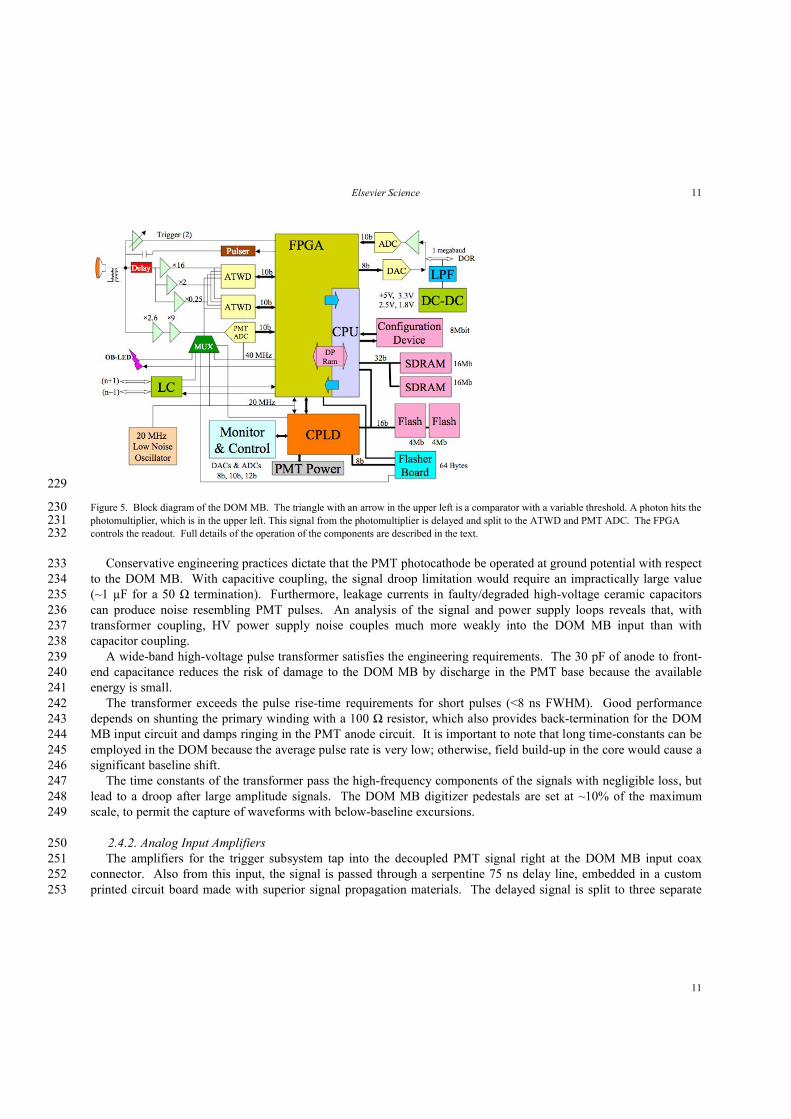
The DOM MB’s primary components are identified in Figure 4, while the functional blocks are shown in Figure 5. 209The top of Figure 5 shows that the analog signal from the PMT is split into three paths at the input to the DOM MB. 210The top path is for the trigger. Below it is the main signal path which goes through a 75 ns delay line and is then split 211and presented to three channels of the two ATWDs after different levels of amplification. Finally, a part of the PMT 212signal is sent to an ADC designed for handling longer signals and a lower sampling speed than the ATWDs. These 213signal paths, the electronics needed to digitize them and send the Hits to the surface, and some additional circuitry are 214described in the following subsections.215
Elsevier Science10
10
216
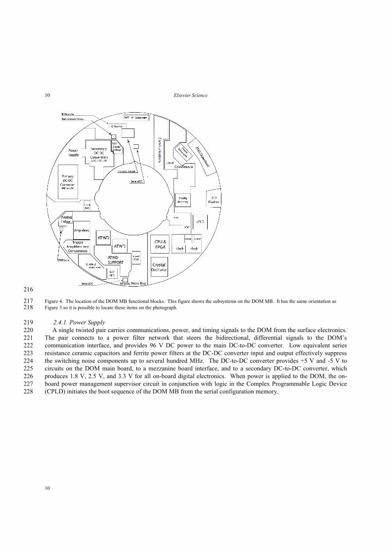
Figure 4. The location of the DOM MB functional blocks. This figure shows the subsystems on the DOM MB. It has the same orientation as 217Figure 3 so it is possible to locate these items on the photograph.218
2.4.1. Power Supply219A single twisted pair carries communications, power, and timing signals to the DOM from the surface electronics. 220
The pair connects to a power filter network that steers the bidirectional, differential signals to the DOM’s 221communication interface, and provides 96 V DC power to the main DC-to-DC converter. Low equivalent series 222resistance ceramic capacitors and ferrite power filters at the DC-DC converter input and output effectively suppress 223the switching noise components up to several hundred MHz. The DC-to-DC converter provides +5 V and -5 V to 224circuits on the DOM main board, to a mezzanine board interface, and to a secondary DC-to-DC converter, which 225produces 1.8 V, 2.5 V, and 3.3 V for all on-board digital electronics. When power is applied to the DOM, the on-226board power management supervisor circuit in conjunction with logic in the Complex Programmable Logic Device 227(CPLD) initiates the boot sequence of the DOM MB from the serial configuration memory. 228
Elsevier Science 11
11
229
Figure 5. Block diagram of the DOM MB. The triangle with an arrow in the upper left is a comparator with a variable threshold. A photon hits the 230photomultiplier, which is in the upper left. This signal from the photomultiplier is delayed and split to the ATWD and PMT ADC. The FPGA 231controls the readout. Full details of the operation of the components are described in the text.232
Conservative engineering practices dictate that the PMT photocathode be operated at ground potential with respect 233to the DOM MB. With capacitive coupling, the signal droop limitation would require an impractically large value 234(~1 µF for a 50 Ω termination). Furthermore, leakage currents in faulty/degraded high-voltage ceramic capacitors 235can produce noise resembling PMT pulses. An analysis of the signal and power supply loops reveals that, with 236transformer coupling, HV power supply noise couples much more weakly into the DOM MB input than with 237capacitor coupling.238
A wide-band high-voltage pulse transformer satisfies the engineering requirements. The 30 pF of anode to front-239end capacitance reduces the risk of damage to the DOM MB by discharge in the PMT base because the available 240energy is small.241
The transformer exceeds the pulse rise-time requirements for short pulses (<8 ns FWHM). Good performance 242depends on shunting the primary winding with a 100 Ω resistor, which also provides back-termination for the DOM 243MB input circuit and damps ringing in the PMT anode circuit. It is important to note that long time-constants can be 244employed in the DOM because the average pulse rate is very low; otherwise, field build-up in the core would cause a 245significant baseline shift.246
The time constants of the transformer pass the high-frequency components of the signals with negligible loss, but 247lead to a droop after large amplitude signals. The DOM MB digitizer pedestals are set at ~10% of the maximum 248scale, to permit the capture of waveforms with below-baseline excursions.249
2.4.2. Analog Input Amplifiers250The amplifiers for the trigger subsystem tap into the decoupled PMT signal right at the DOM MB input coax 251
connector. Also from this input, the signal is passed through a serpentine 75 ns delay line, embedded in a custom 252printed circuit board made with superior signal propagation materials. The delayed signal is split to three separate 253
Elsevier Science12
12
wide-band amplifiers (16, 2, and 0.25), which preserve the PMT analog waveform with only minor bandwidth 254losses. Each amplifier sends its output to separate inputs of the ATWD. The amplifiers have a 100 MHz bandwidth, 255which is roughly matched to the 300 MSPS ATWD sampling rate256
The circuitry confines the ATWD input signal within a 0 to 3 V range. If the input voltage were below –0.5 V, 257then the ATWD could be driven into latch-up; an input signal above 3.3 V would drive the ATWD into an operating 258condition from which it would recover slowly. Resistor-diode networks protect the inputs of the amplifiers from 259spikes, which might be produced by the PMT, or from static discharge.260
2.4.3. ATWD261The ATWD, which is a custom designed ASIC, is the waveform digitizer for four analog inputs. Its analog 262
memory stores 128 samples for each input until it digitized or discarded. Three amplified PMT signals provide the 263input to the first three ATWD channels. In addition, two 4-channel analog multiplexer chips, which can be 264individually selected, are the fourth input channel. The ATWD is normally quiescent, dissipating little power, and 265awaits a trigger signal before it converts the data to a digital signal266
A transition of the PMT discriminator initiates the waveform capture sequence by triggering an ATWD capture. 267The actual ATWD launch is resynchronized to a clock edge to eliminate ambiguity in timestamps. Capture results in 268128 analog samples in each of the four channels. After capture is complete, digital conversion is optional, and may 269be initiated by the FPGA’s (see Section 2.4.8) ATWD readout engine only if other logical conditions are met, as 270determined by the local coincidence settings and operating mode of the array (see Section 4.4). If the subsequent 271trigger-to-conversion conditions are not met, firmware in the FPGA resets ATWD sampling circuitry in two counts of 272the 40 MHz clock.273
If trigger conditions lead to ATWD digitization, 128 Wilkinson 10-bit common-ramp analog to digital converters 274(ADCs) internal to the ATWD digitize the analog signals stored on a selected set of 128 sampling capacitors. The 275digital data are stored in a 128-word deep internal shift register. 276
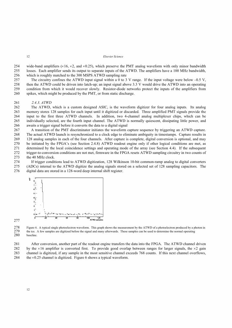
277
Figure 6. A typical single photoelectron waveform. This graph shows the measurement by the ATWD of a photoelectron produced by a photon in 278the ice. A few samples are digitized before the signal and many afterwards. These samples can be used to determine the normal operating 279baseline.280
After conversion, another part of the readout engine transfers the data into the FPGA. The ATWD channel driven 281by the 16 amplifier is converted first. To provide good overlap between ranges for larger signals, the 2 gain 282channel is digitized, if any sample in the most sensitive channel exceeds 768 counts. If this next channel overflows, 283the 0.25 channel is digitized. Figure 6 shows a typical waveform.284
Elsevier Science 13
13
Including the analog to digital conversion, transfer to the ATWD, and incidental overhead, the ATWD takes 29 s 285to digitize a waveform after capture. These parallel signal paths have the dynamic range of a 14-bit 300 MSPS ADC 286while consuming only ~150 mW of power without any high-speed clock or digital memory requirement. To 287minimize dead time, the DOM is equipped with two ATWDs such that while one is processing input signals, the 288other is available for signal capture.289
2.4.4. High-speed Monitoring With the ATWD Multiplexer290The fourth ATWD channel is driven by either of two 4-channel analog multiplexers, permitting measurement from 291
eight signal sources on the DOM MB. Multiplexer channel 0 carries the 20 MHz signal from the internal clock 292oscillator, as a sine wave. Channel 1 carries the frequency-doubled output of the internal FPGA phase-locked loop 293(PLL). These signals allow the ATWD capture sampling rate calibration, the verification of the phase of ATWD 294capture, and the clock phase for PMT waveform capture by the PMT ADC (see Section 2.4.5).295
Signals from the on-board and the off-board LED flasher switch circuits, multiplexer channels 2 and 3, make 296possible the measurement of PMT transit time, and the timestamping of flasher signals targeted at neighboring DOMs 297in the array. 298
Signals from the local coincidence transceivers (see Section 4.4) appear on channels 4 and 5. These signals 299provide diagnostic waveforms for assessing possible fault conditions with the local coincidence subsystem.300
The communications transceiver signal on channel 6 allows calibration of the Hit timestamp with respect to the 301precisely timed RAPcal calibration pulses transmitted to the DOM from the ICL.302
Channel 7 monitors the output of an arbitrary waveform generator, driven by FPGA code. 303Bits written to registers in the DOM MB CPLD separately enable each multiplexer, and select the appropriate 304
channel to be digitized. To save power, the multiplexers are shut down when not in use.305
2.4.5. PMT ADC306Some physics signals last longer than can be captured by the ATWD. To obtain this information, there is a fourth 307
PMT signal path. This path consists of a three-stage waveform-shaping amplifier with a 180 ns shaping time. This 308path drives a low power, high-speed, 10-bit wide, parallel output, and pipelined “PMT ADC”. The PMT ADC 309continuously samples the bandwidth-limited PMT output signal at 40 MSPS.310
DOM MB electronics downstream can record an arbitrarily long PMT ADC record in response to a trigger, but the 311length of the raw PMT ADC record is chosen to be 6.4 s. The DOM MB is capable of triggering two clock cycles 312after digitizing a previous event.313
An SPE signal from the PMT produces approximately a 13-count value above the ADC’s baseline, sufficient to 314detect its presence. This relatively low gain allows the PMT ADC to offer reasonable dynamic range.315
2.4.6. PMT Trigger Discriminator316The DOM MB can trigger on signals from the PMT. To do this, it uses a signal from the PMT, which drives the 317
amplifier stages preceding two low power, high-speed comparators (discriminators). Each comparator has a different 318sensitivity. The high-resolution comparator, with a nominal 0.0024 PE/DAC count, has a narrow operating range, 319and is intended to sense SPE pulses. The low-resolution “multi-PE” comparator has a resolution that is coarser by a 320factor of 10 and therefore has a wider operating range.321
At the nominal InIce PMT gain of 1 107, the low system noise and low device noise allow the PMT trigger level 322to be set as low as 1/6 SPE. At this threshold, there is no significant increase in trigger rate due to electronic noise.323
Elsevier Science14
14
Also, these two comparators enable the implementation of multi-level event recognition. For example, the IceTop 324high gain DOMs (5 106) utilize the multi-PE discriminator for triggering, with its threshold set to an amplitude 325corresponding to a pulse of 10 PEs. In addition, these two comparators are used in self-local coincidence mode, 326which is described in Section 4.4.3.327
2.4.7. Local Coincidence Trigger Circuit328When a trigger comparator fires, two state machines are activated to send local-coincidence digital signals to 329
adjacent DOMs (above and below) through bidirectional, fully duplex transceivers connected to a dedicated network 330of twisted wire pairs.331
Local coincidence receivers on each DOM deliver signals into the trigger system of the FPGA and into a relaying 332state machine. This local coincidence relaying engine, if enabled, forwards a message beyond the nearest neighbor 333DOM. The scheme makes possible coincidence between nearest neighbors, next-nearest neighbors, and so on. If a 334DOM originates and transmits a local coincidence (LC) signal, it will not relay the redundant LC signals from its 335neighbors. 336
2.4.8. FPGA and ARM CPU337The Altera EPXA-4 FPGA handles signal and communications processing. The CPU handles data transport, 338
system testing and monitoring. The CPU initiates FPGA reconfiguration, in real-time, as dictated by the 339requirements of data acquisition and system testing. This highly integrated system on a programmable chip (SOPC) 340architecture confines high speed, high data bandwidth signals to a single die on the DOM MB, which reduces noise 341and saves power.342
The Hit processing portion of the FPGA contains trigger logic, an ATWD readout engine for each ATWD, a Hit 343record building engine, a data compression engine, and a direct memory access (DMA) controller. A DMA engine 344transfers Hit records into main memory for subsequent transmission to the ICL. It also implements on-board and off-345board flasher control logic, PMT ADC data handling, communications protocol state machines, communications 346ADC, and DAC data handling.347
The communications processing portion of the FPGA contains a half-duplex signaling protocol engine and 348modulation and demodulation function blocks, which drive a communications digital to analog converter (DAC) and 349monitor a communications ADC respectively.350
The Altera chip also provides IceCube with a supernova (SN) search capability. A SN event, if yielding a 351sufficiently intense flux of MeV neutrinos at earth, will cause a global increase in the ambient light deep in the ice. A 352rate increase, seen by all DOMs, provides an unambiguous signal for such an event. The chip records the rate of Hits 353- binning Hit times at the few ms level.354
2.4.9. Memory (SDRAM, Flash, Flash Files)355The EPXA-4 architecture supports SDRAM (synchronous dynamic random access memory) for main memory, an 356
SRAM (static random access memory) interface for low-performance memory, memory-mapped peripherals, and 357flash memory. The DOM MB includes two 16 MB SDRAM memory chips, two 4 MB flash (non-volatile) 358memories, and a 4 Mb configuration memory.359
When the DOM is powered up, the serial configuration memory uploads a configuration into the EPXA4's FPGA 360and program code into the EPXA4's CPU's memory. The configuration memory can only be programmed before the 361DOM is sealed and cannot be reprogrammed after deployment. Its contents include a base-band communications 362package for the FPGA, a utility program for the CPU so that the flash memory chips are loaded, and a command 363
Elsevier Science 15
15
interpreter for rebooting to the boot-block in either flash memory. This is analogous to a desktop computer booting 364to block 0 of its hard disk. 365
The two 4 MB boot-block flash memories are organized as a log structured flash memory file system. The file 366system stores CPU programs, FPGA configuration files, and interpreter scripts. Various files support production 367testing, integration after deployment, and Hit data acquisition. Any and all files may be updated after the DOM is 368deployed into the ice. Each flash memory also contains a 64-bit serial number, from which we derive a unique 48-bit 369DOM ID. The DOM ID maps to the geometrical position of each DOM. Furthermore, unique DOM parameters can 370be loaded by DAQ control from a database indexed by the DOM ID.371
After reboot, the CPU executes program code copied into SDRAM. Approximately half of the SDRAM is 372allocated as a circular buffer for DMA Hit record transfers from the FPGA. The CPU accesses registers in the CPLD 373and Flasher Board interface through the Expansion Bus Interface (EBI). Flash memory also resides on the EBI.374
2.4.10. DOM Local Oscillator375The DOM’s 20 MHz temperature-compensated crystal oscillator has a certified stability of roughly 1 × 10-11 for a 376
sample interval of 5 seconds.8 In practice, the crystal frequency and phase drifts become significant typically only 377after several minutes. The 20 MHz oscillator output drives the clock inputs of the FPGA, the communications ADC, 378the communications DAC, and the reference clock signal port of the flasher board interface. A phase locked loop 379(PLL) in the FPGA doubles the frequency to 40 MHz. This 40 MHz signal drives a 48-bit local clock within the 380FPGA, the DOM local clock; it rolls over every 81.4 days. The DOM local clock is used to timestamp Hits recorded 381by the DOM and the RAPcal timing calibration packets exchanged between the DOM and the DOMHub. The 40 382MHz reference also drives the clock input of the PMT ADC. 383
2.4.11. Communication With Surface384As communication and power must share the same wire pair, it is necessary to separate them at the DOM MB. 385
Balanced L sections at the power filter input confine the communications signals to the communications front-end 386receiver. A section filters the power and isolates the DOM communications interface from switching noise.387
Ceramic capacitors couple communications signals between the twisted pair and the communications transformer.388The grounded center tap of the transformer accommodates the topology required by the 8-bit current-mode 389communications DAC clocked at 20 MHz. The choice of current mode DAC allows two DOMs to share the InIce 390end of the main cable pair. The end-most DOM on the pair must be terminated in the characteristic impedance of the 391twisted pair. The unterminated DOM typically bridges onto the twisted pair 17 meters upstream from the terminated 392DOM; the additional stub introduces a small, systematic time error. The modulator produces differential signals with 393amplitudes of approximately 2 V (depending on communications parameter settings) onto the twisted pair.394
The center-tapped secondary of the transformer also drives a 5 differential amplifier stage characterized by high 395common mode rejection ratio (CMRR). The high CMRR reduces the susceptibility of the DOM line receiver to 396interfering signals such as electromagnetic interference (EMI) or radio frequency interference (RFI). The amplifier 397drives a 10-bit, 2 V input-span, ADC that samples the communications waveform at 20 MSPS. The parallel output 398stream of ADC data drives the inputs of the communications receiver firmware in the FPGA. 399
8
Vectron International manufactures the model C2560A-0009 TCXO module specifically for IceCube. Since the oscillator is crucial to DOM performance, the brand and model were selected based on Allen variance performance and power consumption. The procurement specification required 100% Allen variance testing.
Elsevier Science16
16
The topology resembles that of the commonly used T-1 communications links. So, the natural choice was 400Amplitude Shift Keying9 (ASK) with a transmission rate of 1 Mb/s, which includes encoding bits. Since we have 401selected ASK modulation, and multiple DOMs share wire pairs, it is necessary to utilize half-duplex. The 402communications master resides in the communications card within the DOMHub in the ICL. That master alternately 403sends commands to and requests data from the two DOMs sharing the InIce end of the wire pair.404
The distribution rate of RAPcal signals from the ICL to all DOMs must accommodate any oscillators with 405marginal short-term stability. The stability requirement for the DOM local oscillator is that RAPcal signals be 406distributed to all DOMs in the array at least as often as every 5 seconds. However, the complete DOMHub-to-DOM-407to-DOMHub exchange of RAPcal signals consumes less than 1.5 ms, so the sacrifice of system communications 408bandwidth to time calibration is negligible.409
2.4.12. CPLD410The DOM depends upon certain higher-level logic functions and state machines that cannot be implemented in the 411
FPGA because the FPGA does not retain its logic configuration through power cycling. Those logic functions are 412implemented in a CPLD.413
The CPLD code contains a state machine that controls the booting of the EPXA4, initiated by the rising edge of 414the not-power-on-reset (nPOR) signal of the power supervisor chip. The logic in the CPLD assures that all power 415supplies are at voltage and stable, and that internal initialization of other complex components of the DOM has been 416completed before the configuration memory uploads its contents into the EPXA4’s CPU and FPGA configuration.417
The CPLD code also contains an interface between the EBI memory bus and the high-speed interface connector 418used by the external LED Flasher Board. The bus interface prevents possible catastrophic failure of the flasher or a 419generic daughter card from disrupting the memory bus the CPU relies upon for booting to its normal running–mode 420configuration which is read from flash memory. 421
The applications programmer interface (API) of the CPLD appears to the CPU as read-only and write-only 422memory in EBI address space. Control register bits enable or disable the high voltage power interface for the PMT, 423the voltage source for the on-board LED flasher, the Flasher Board interface, and the pressure sensor. 424
The CPLD firmware controls the reading of 24 channels of the slow (serial) ADC used for monitoring and 425diagnostic purposes. It also sets the 16 slow (serial) DAC outputs used to control ATWD operating parameters, 426trigger comparator levels, and ADC reference levels. A separate serial interface supports the control and read-out of 427PMT high voltage module. 428
The CPU may control whether it reboots from the serial configuration memory (boot to Configboot), or to flash 429memory (boot to Iceboot), by executing a CPLD function. Another CPLD function actually initiates reboot. 430
The CPU may boot from either of the two flash memory chips. The Configboot program supports a CPLD 431function, which virtually exchanges flash-0 for flash-1, allowing the recovery from failure of the flash-0 boot block 432subsequent to deployment.433
Several registers contain read-write scratch-pad bits. Scratch-pad data are retained through reboot, allowing a 434limited amount of crucial context information that can be retained through reboot.435
9 The communications interface design is compatible with phase modulation schemes, which offer higher data rate, superior noise immunity and timing precision, as well as full duplex communications.
Elsevier Science 17
17
2.4.13. On-board Electrical Pulser436Many DOM calibration programs depend upon a built-in signal source that produces waveforms similar to SPE 437
PMT pulses. The pulser injects charge that is stored on a capacitor into the analog input of the DOM MB, at the 438PMT cable connector. A serial DAC, controls the pulser amplitude up to roughly 40 PE, in 0.04 PE steps. 439
The shape design was based upon previous measurements. Care was taken to minimize noise into the DOM MB 440when the pulser was activated. Recent results show that the pulser shape is slightly wider than an actual PMT shape. 441
2.4.14. On-board LED pulser442Each DOM MB includes a pulse forming circuit driving an ultraviolet LED that has a wavelength of 374 nm. The 443
function of the on-board LED pulse is to stimulate the local PMT, whereas the function of the Flasher Board is to 444stimulate neighboring DOMs. 445
A state machine in the DOM initiates a trigger, and simultaneously sends a trigger pulse to the LED flasher circuit. 446The flasher circuit dumps a current pulse into the LED via a "shunt" which produces a voltage pulse across it. The 447pulse propagates from the pulser circuit to the MUX connected to ATWD channel number 4. The LED flash 448produces light, which bounces over to the PMT. The ATWD simultaneously captures PMT input and the current 449shunt input. The time difference between the current pulse and the PMT pulse is the transit time of the PMT, delay 450line, other circuit components.451
The LED flash brightness can be adjusted to produce zero to a few tens of photoelectrons at the photocathode of 452the PMT. The brightness range of the on-board LED is sufficient to measure the transit time over several orders of 453magnitude of PMT gain around the typical operating point. Controlled weak flashes (optimally around 1% 454occupancy) makes possible the assessment of the SPE behavior of the PMT. 455
2.4.15. Interface to PMT Power Supply Daughter-card456The DOM MB controls and powers the PMT HV subsystem, which resides on a mezzanine card atop the Flasher 457
Board. The control signals, the serial bus signals, system ground, and raw power are delivered to the HV module 458through a ribbon cable. 459
The CPLD of the DOM MB contains a control register with one bit allocated to enable the high voltage control 460board, and another bit allocated to enable the high voltage output of the high voltage module on the HV control 461board. The HV control board contains two synchronous serial (SPI protocol) devices, a serial DAC for high voltage 462control, and a serial ADC for monitoring the HV module output voltage. 463
The serial bus clock, control, and data lines of the HV subsystem interface use CPLD pins and firmware that is 464independent of the on-board monitoring serial bus, which is also supported by the CPLD and firmware. This feature 465prevents a failure causing disruption of the on-board serial bus from interfering with the operation of the high voltage 466subsystem, and vice-versa. The CPLD firmware also contains code to read the serial number chip built into the HV 467interface card.468
2.4.16. Interface to the Flasher Board; a Generalized High-speed Interface469The DOM MB includes a 48 pin, high-speed, memory mapped interface to the Flasher Board. The connector 470
delivers power, an extension of the EBI memory bus, and control lines from the DOM MB FPGA to the daughter 471card. The connector also delivers system clock and trigger control signals directly from the FPGAs.472
This interface delivers a power-enable line to the daughter card. When this line goes high, the daughter- card is 473permitted to draw power and connect to the memory bus interface. Likewise, an enable is transferred to the bus 474
Elsevier Science18
18
extension enable firmware in the CPLD. This feature allows a 30% saving of power, since the calibration capability 475provided by the high intensity flashers is rarely needed.476
When the power-enable line goes low, the daughter card powers off all electronics, and disconnects from the bus 477extension. If the DOM power supervisor should detect an event that causes nPOR to be asserted, then the power-478enable line is set to the default (low state) and the memory bus repeater built into the CPLD breaks connection with 479the EBI memory bus. This buffering feature protects the primary data-taking capability of the DOM MB from being 480compromised should there be a catastrophic failure of the flasher card.481
The interface has 8 bidirectional data lines, a read line, a write line, and 6 address lines to the daughter card. This 482is sufficient to control a wide variety of states in the daughter card, as well as permitting the transfer of arbitrarily 483large data sets in either direction. The data requirements of the Flasher Board are, however, modest.484
Control lines from the FPGA of the DOM MB notify the Flasher Board when to initiate a flash. The Flasher 485Board produces an output pulse whose voltage is proportional to the flash amplitude. That signal is sent through a 486coax cable to a multiplexer input of the ATWD for timing calibration purposes.487
The interface includes a low-voltage differential signal (LVDS) 20 MHz clock pair derived from the DOM MB 488system clock. This feature is useful for synchronizing it with the DOM MB activity. It also contains a set of control 489and I/O lines configured as a JTAG10 programming interface. The interface allows firmware to be updated in the 490flasher board after the DOM has been deployed in the ice.491
2.4.17. Monitoring with the Slow ADCs 492Two serial ADCs (I2C protocol) monitor a total of 24 voltages in the DOM. The ADC readouts are particularly 493
useful in the test stage of newly manufactured DOM MBs. They also provide some diagnostic information should 494the DOM suffer a partial failure after deployment. 495
Channels 0, 1, 9, 10, and 11 monitor power supply voltages. Channel 2 monitors the (DOM) pressure sensor on 496the DOM MB. The voltage measurement on Channel 0 is necessary to calibrate the pressure measurement.497
Channels 3, 4, 5, 6, and 7 monitor the current delivered by all major power supplies on the DOM MB. Channels 8 498and 12 monitor control voltages of the front-end discriminator thresholds. Channel 13 monitors the reference voltage 499of the high speed ADC. Channel 14 monitors the voltage delivered to the on-board LED pulser. Channels 15-22 500monitor control voltages produced by serial DACs, which control ATWD behavior. Finally, channel 23 monitors the 501voltage of the front-end test-pulse control.502
2.5. The Cable Network 503
The cable network carries power and signals between the DOMs and the DOMHub. The cable is of sufficient 504quality that the amplitude-shift modulation scheme reliably yields data rates up to ~900 kb/s for the most remote 505DOMs in the array. By sharing two DOMs on one pair, only one cable is needed for a string, substantially reducing 506costs. This cable size, roughly 3 cm in diameter, approaches the practical limits for transportation volume and weight, 507flexibility, and strength during deployment.508
The down-hole cable consists of 20 quads. Fifteen quads are used for signals to the DOMS while one is for LC. 509Each quad contains two pairs of wires. The DOM Quad services four DOMs. Three twisted pairs from the cable 510enter the DOM in the location identified as the Cable Penetrator Assembly seen in Figure 2. Two of these pairs are 511the LC links to adjacent DOMs; the third pair connects the DOM to the DOMHub.512
10 Joint Test Action Group IEEE Standard 1149.1-1990.
Elsevier Science 19
19
A surface cable from ICL connects to a surface junction box located near the top of each hole. The surface cable 513contains extra wire quads in an inner, shielded core to service the two IceTop tanks associated with each hole. Data 514rates for IceTop DOMs are higher than for InIce DOMs, so only one IceTop DOM is connected to its corresponding 515DOR card input. However, to maintain commonality throughout IceCube, the control and communications protocol 516and baud rate are the same as for cable pairs. IceTop DOMs also exploit an LC communication link between the two 517tanks at each station.518
519
Figure 7. A block diagram of the DOMHub. The left hand side depicts the data from a string of DOMs. The label 2 in the left circles refers to the 520fact that two DOMS are on each wire pair. The number 4 refers to the fact that each DOR card digitizes four DOM pairs. The DOM Hub contains 521a power supply, a CPU Card and the DSB card for timing. The DOR cards communicate over the backplane. A DOMHub communicates with the 522trigger and event builder over Ethernet.523
2.6. The DOMHub 524
The DOMHub is a computer in the ICL that communicates with all of a string’s DOM MBs. Its block diagram 525can be seen in Figure 7. Its components are housed in a standard 24” deep industrial PC chassis. The PCI bus 526backplane accommodates 8 DOR cards, one DOMHub Service Board (DSB), and one low power single board 527computer (SBC).528
Each DOR card can communicate with eight DOMs, so the DOMHub can host 64 DOMs. In practice, a 529DOMHub hosts an entire string of 60 DOMs for InIce, or 32 DOMs for IceTop (8 stations). 530
2.6.1. The DOM Readout (DOR) Card531The DOR card is a full-size full-custom PCI card, shown in Figure 8. Each DOR card handles communications 532
with the DOMs connected to its four wire-pair inputs and the DOR Driver, the lowest level software element of the 533DAQ chain in the ICL. The block diagram in Figure 9 shows the media access interfaces, and power control 534functions of the DOR card.535
Elsevier Science20
20
536Figure 8. A photograph of a fully functional DOR card.537
The DOR card controls power to the DOMs, establishes that boot-up has occurred properly, selects which code the 538DOM is to run (or downloads new code), establishes a conversation that may include calibration tasks or block data 539transfer, senses fault conditions, manages time calibration sequences, controls the DOM state, or initiates any of the 540numerous and diverse DOM actions.541
A utility function loads the FPGA configuration files into flash memory. Other functions cause the 542communications FPGA to be reloaded from flash memory, select the clock source, initiate RAPcal, signal exchanges 543with DOMs, and other features described in the next section.544
545
Figure 9. This figure shows the functional blocks of a DOR Card. On the left shows the signals from the DOMs. The COM ADC/DAQ digitizes 546the signals from the DOMs and sends signals to the DOM over the wire pairs on the quad cable. The Communication FPGA drives these ADCs. 547Memory is shown as well as the exterior communications and power to the DOR card.548
2.6.2. PCI Block549The firmware of the PCI bus interface FPGA includes a commercial VHDL PCI core adapted to suit the 550
requirements of the DOR card hardware and DOR driver. The 32-bit core supports master/slave control logic, and 33 551MHz bus speed. The PCI core is compliant with “PCI Local Bus Specification revision 2.2”.552
Elsevier Science 21
21
The PCI FPGA executes bi-directional programmed (single bus cycle) 32-bit transfer to thirty-two control and 553status registers. The firmware also contains code for 32-bit quad-word aligned DMA (Direct memory access) writes 554of data to main memory on the CPU board in the PC chassis. 555
2.6.3. DOM Power Management556The DOR driver can cause the ±48 V power for any of the 4 wire pairs to be switched on or off. Both wires of a 557
pair are switched for symmetry and safety. Also, for safety, power is applied only when a cable connection is sensed. 558The switches have built-in slew-rate limiting to reduce component stresses, and suppress power on/off transient 559noise.560
The DOR card has ADC’s for monitoring wire pair current and voltage. A “proc file” interface of the DOR driver 561allows the voltage and current values to be read by user programs, or from the command line. Furthermore, a 562firmware component detects pair over- current or under-current conditions and then removes power to the pair.563
2.6.4. DSB Card564The DSB card is a very simple electronics board. Its primary function is to distribute the system timing and 565
reference signals to each of the eight DOR cards in a DOMHub. The inputs to this board include the 10 MHz system 566clock, 1 Hz, and Global Position System (GPS) reference signal (see Section 2.7). These signals originate in a GPS 567receiver in the ICL and are distributed isochronously to all DOMHubs.568
2.6.5. Time Calibration569The DOR card receives the clock signals from the DSB Board. A PLL on the DOR card produces the 20 MHz 570
global clock, which drives the 56-bit clock counter in the communication FPGA of each DOR card. The 1 Hz signal 571triggers a snapshot of the 56-bit counter value every second. The DOR clock counter rolls over every 114.24 years, 572and is never explicitly reset. The counter snapshots together with the corresponding encoded time of day provide a 573cross reference between the DOR card’s local clock value and the UTC time.574
Software may initiate a time calibration. The DOR firmware completely manages the time calibration process. 575The cycle produces a RAPcal data packet containing DOR and DOM timestamps and digitized RAPcal received 576pulse waveforms.577
2.6.6. DOR card Flash Memory and FPGA Configuration578The communications controller FPGA configuration image resides in page 0, 1, or 2 of a 2 MB Flash memory. 579
The PCI bus interface FPGA image resides in page 3. Loading the communications image into flash depends on the 580integrity of the PCI image. Consequently, the PCI image is protected.581
The two FPGAs and the CPLD share a JTAG chain. At time of DOR card manufacture, first, the CPLD must be 582programmed via JTAG, and then the PCI FPGA must be loaded via the JTAG. Power must be kept on until flash is 583loaded. UNIX utility programs write configuration files to flash memory pages through the DOR Driver’s Linux file 584system proc file interface. Validity checking in the DOR Driver prevents invalid images from being loaded into 585DOR card flash. The JTAG chain provides a means for loading test firmware into either FPGA.586
Once flash is loaded, the application of power, or a PCI bus reset, causes a CPLD on the DOR card to read 587configuration data from flash memory, serialize it, and transfers it to an in-circuit programming interfaces of each 588FPGA. The communications FPGA may be reloaded at any time by issuing a command to the DOR Driver; the PCI 589FPGA may be reloaded on the fly, but this is risky in case the new image contains a bug.590
Elsevier Science22
22
Each DOR card, after final assembly and test, has a unique ID, as well as a final test summary, written into the 591uppermost 64 K byte sector of the flash memory. The code contains the card revision number, the production run 592number, and the card serial number, which matches the card’s label. The production information may be read from 593the DOR driver proc file interface.594
2.7. The Master Clock and Array Timing595
The two central components of the IceCube timing system are the Master Clock, providing each DOMHub with a 596high precision internal “clock” synchronized to UTC [11] and the calibration process RAPcal described in Section 5974.7. Together, these manage the time calibration as a “background” process, identically for InIce and IceTop.598
The Master Clock makes use of the Global Positioning System (GPS) satellite radio-navigation system, which 599disseminates precision time from the UTC master clock at the US Naval Observatory to our GPS receiver in the ICL. 600Algorithms in the GPS receiver clock circuit make small, but abrupt, changes to crystal oscillator operating 601parameters according to a schedule optimized for GPS satellite tracking. The abrupt parameter changes, and phase 602error accumulation intervals result in deviations from UTC of typically 40 ns RMS over time scales of hours, but not 603exceeding 150 ns.604
The GPS reference time for IceCube is the phase of the 10 MHz local oven-stabilized crystal reference oscillator 605in the GPS receiver. This oscillator is optimized for excellent Allen variance performance. Altogether, the system 606delivers an accuracy of about ±10 ns averaged over 24 hours.607
The fan-out subsystem distributes the 10 MHz, the 1 Hz (as a phase modulated 10 MHz carrier), and encoded 608time-of-day data from the GPS receiver to DOMHubs through an active fan-out. The encoded GPS time data, 609contains second, minute, and hour of the day, day of the year, and a time quality status character. 610
The principal engineering requirements for the fan-out are low jitter, high noise immunity, simplicity, and 611robustness. The 10 MHz and 1 Hz modulated 10 MHz signals pass through common mode inductors at the 612transmitter and receiver end to improve noise immunity and effectively break ground loops between apparatus widely 613dispersed in the ICL. For the encoded time of day information, RS-485 was chosen for its noise immunity. Each 614distribution port of the fan-out has its own line drivers to insure that any particular failure has minimal impact on 615neighboring distribution ports.616
The Master Clock Distribution System and interconnecting cables delay the arrival of time reference signals 617traveling from the GPS receiver to the DOMHub. All signal paths between the GPS receiver’s 10 MHz output, via 618fan-outs to the DSB, and to each DOR card are matched within 0.7 ns RMS. Thus, the DOR cards “mirror” the 619Master Clock with an accuracy of less than 1 ns.620
A static offset must be applied to the experimental data to map IceCube Time (ICT) to UTC. ICT differs from 621UTC by the master clock distribution cable delay plus the GPS to UTC offset.622
The DSB card in each DOMHub distributes the three signals to each of the eight DOR cards. The DOR card 623doubles the GPS frequency to 20 MHz and drives a clock counter. When the 10 MHz clock signal goes high 624immediately after the 1 Hz GPS signal goes high, logic in the DOR card’s FPGA latches the clock counter value and 625the time of day data from the GPS receiver from the previous second to form a time sample record. This time 626sampling engine stores its output in a 10-reading deep first-in first-out (FIFO) memory. Data acquisition software 627running in a DOMHub’s CPU reads these records from a Linux file system proc file and forwards them to a data-628logging computer where they become part of the physics data set.629
Elsevier Science 23
23
In operation, the clock counter value in each DOR card increments exactly 2 107 counts every second. A 630module in the DOR card firmware confirms that 2 107 additional counts are registered each second to verify clock 631integrity, and firmware correctness, and freedom from injected noise. 632
3. Firmware and Software633
In the universe of computers, the DOM resembles a hand held device since it does not have a mass storage device 634like a disk drive. The DOM does not need “processes” in the sense of UNIX, nor “task scheduling.” However, 635interrupt handlers are used for communications and data collection. Therefore, an open source collection of standard 636UNIX-like single threaded functions called "newlib" [12] was chosen instead of more sophisticated embedded 637operating systems like Windows CE, embedded LINUX, or NetBSD. Newlib functions streamline common tasks 638such as memory allocation and string operations. Communications on the DOM side, including a custom 639communications protocol, are largely implemented in FPGA firmware. 640
3.1. DOM Software641
At power on, firmware embedded in the Altera EPXA4 chip (called the logic master) copies a simple, robust 642bootstrap program named Configboot from a read-only serial configuration memory into internal SRAM, configures 643the FPGA, and initiates the execution of program code at the start of SRAM. The Configboot program interprets a 644very small set of terse commands that allow the DOM to reboot to the image in the boot block of the primary flash 645memory, boot from other locations in either flash memory, or boot from a dedicated serial port. A Configboot646command allows reprogramming flash memories via the communications interface to allow the users to easily 647upgrade a DOM with new operating software and firmware. Furthermore, if flash chip 0 were to fail, Configboot can 648be configured to boot the DOM’s CPU from flash chip 1.649
Each DOM uses a reliable, journaling flash file system spanning the pair of flash memories into which a release 650image is loaded. The release image consists of data files, software programs for test and data acquisition, and FPGA 651configurations that suit the requirements of the software programs. The release file is built on a server computer from 652components of a software development archive. 653
Booting from flash block 0 causes the DOM’s CPU to copy a fully featured program, called Iceboot, into 654SDRAM, and start executing it. The program Iceboot is built of layers: low-level bootstrap code; Newlib code; a 655Hardware Access Layer (HAL) used to encapsulate all hardware functions provided by the CPLD; the application 656program/server; and the FPGA, including the communications interface. The Iceboot program presents a Forth 657language interpreter to the user. From the interpreter’s prompt, one can invoke HAL routines directly, write data to, 658and read data from memory addresses, reconfigure the FPGA, and invoke other applications programs like the DOM 659Application (Domapp) used for data acquisition.660
The Domapp program implements a simple binary-format messaging layer on top of the DOR to DOM error-661correcting communications protocol. Messages are sent to particular "services" within the Domapp (e.g. "Slow 662Control", "Data Access"). Each message targets a particular function (e.g., "Slow Control - set high voltage" or 663"Data Access - fetch latest Hit data"). Every message to the DOM generates a single response, and no DOM sends 664data unless queried. Messages are provided for configuring the hardware and for collecting and formatting the 665physics data from buffers in main memory. Other messages provide for buffering and retrieving of periodic 666
Elsevier Science24
24
monitoring data describing the DOMs internal state and any exceptional conditions that may occur. The message can 667be logged or acted upon by the DAQ components in the ICL.668
Typically, between runs, the DOM is rebooted into Iceboot to guarantee its state at the beginning of each run. 669Should the DOM become unresponsive, a low-level communications message sent directly to the communications 670firmware in the FPGA will force the DOM to reboot to Iceboot. Power cycling of the DOM is seldom necessary to 671reinitialize the DOM, and is avoided to minimize electrical stress.672
3.2. DOM Firmware673
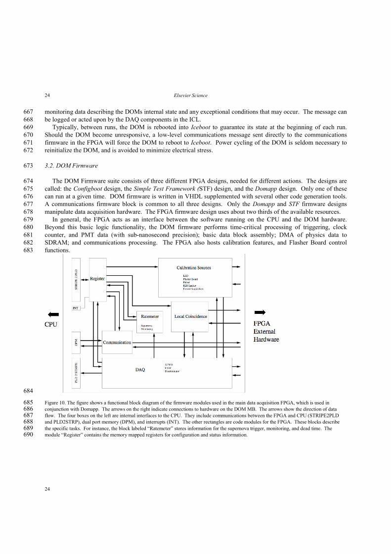
The DOM Firmware suite consists of three different FPGA designs, needed for different actions. The designs are 674called: the Configboot design, the Simple Test Framework (STF) design, and the Domapp design. Only one of these 675can run at a given time. DOM firmware is written in VHDL supplemented with several other code generation tools. 676A communications firmware block is common to all three designs. Only the Domapp and STF firmware designs 677manipulate data acquisition hardware. The FPGA firmware design uses about two thirds of the available resources.678
In general, the FPGA acts as an interface between the software running on the CPU and the DOM hardware. 679Beyond this basic logic functionality, the DOM firmware performs time-critical processing of triggering, clock 680counter, and PMT data (with sub-nanosecond precision); basic data block assembly; DMA of physics data to 681SDRAM; and communications processing. The FPGA also hosts calibration features, and Flasher Board control 682functions.683
684
Figure 10. The figure shows a functional block diagram of the firmware modules used in the main data acquisition FPGA, which is used in 685conjunction with Domapp. The arrows on the right indicate connections to hardware on the DOM MB. The arrows show the direction of data 686flow. The four boxes on the left are internal interfaces to the CPU. They include communications between the FPGA and CPU (STRIPE2PLD 687and PLD2STRP), dual port memory (DPM), and interrupts (INT). The other rectangles are code modules for the FPGA. These blocks describe 688the specific tasks. For instance, the block labeled “Ratemeter” stores information for the supernova trigger, monitoring, and dead time. The 689module “Register” contains the memory mapped registers for configuration and status information.690
Elsevier Science 25
25
The Configboot FPGA design contains only minimal required functionality to provide communications to the 691DOR card. Implementation of a simple, reliable, and robust design was a firm requirement because Configboot692cannot be upgraded once a DOM has been deployed into the ice.693
The STF design is used primarily for DOM hardware testing. Software uses the STF program to manipulate, test 694and verify the functionality of each hardware subsystem.695
The Domapp design, shown schematically in Figure 10, provides for data acquisition. Based on the settings of bits 696in memory mapped control registers according to applications programmer interface (API) documentation, the FPGA 697autonomously collects waveforms from the ATWD and the PMT ADC. It processes the waveforms, builds the hit 698record according to a hard-coded template, and transfers the data through DMA to a block of the CPU’s memory. 699Parallel to data acquisition, the firmware supplies PMT count-rate meters, which are read from data registers in the 700API; count-rate metering facilitates the supernovae detection science goal. In addition, the firmware modules control 701the on-board calibration sources and the Flasher Board.702
3.3. DOMHub Software703
Software on the DOMHub builds on the rich set of DOR hardware and firmware functionality. DOMHub 704software consists of a C-language kernel level device driver ("DOR-driver") for the DOR cards and a user-level Java 705application called Stringhub on a Linux server operating system. Stringhub's task is facilitating the higher-level 706configuration control and communications functions to the rest of the IceCube Surface DAQ.707
Specific requirements for DOR-driver include the following:708 support for a few dozen control functions specific to the DOR cards, 709 a clean interface between the hardware and user applications, and 710 concurrent and error-free communications to all attached DOMs at or close to the maximum throughput 711
supported by the hardware.712The first two items are addressed by implementing a tree of control points via the Linux proc file system, a 713
hierarchy of virtual files used for accessing kernel functions without requiring native system calls. This somewhat 714unusual approach allows the Java-based Stringhub to be written without unwieldy native interface modules. This 715simplifies the DOMHub software architecture and provides the added advantage of making it very easy to operate 716DOMs interactively or through a wide variety of test software.717
The utilization of cyclic redundancy codes (CRCs) in the DOM-to-DOR communications stream ensures that 718corrupt data is identified. Acknowledge/retransmit functions similar to TCP/IP in both the DOM software and in 719DOR-driver insure that no communications packets are lost. Packet assembly/disassembly, transmit, acknowledge, 720and retransmit are carried out on all DOMs in parallel, with periodic time calibration operations seamlessly 721interspersed. The asynchronous activity of 8 DOR cards, 60 DOMs, multiple user applications, and many control 722functions create substantial risk of race conditions that are identified and eliminated.723
Extensive testing is crucial for a large device driver such as this one operating on custom hardware (in lines of 724code, DOR-driver is comparable to a Linux Ethernet driver). The first phase of testing addresses long-term stability 725under normal operating conditions with maximum throughput; the second phase of testing emphasizes "torture tests" 726designed to expose unexpected races and edge conditions in the driver and firmware. Every driver-release candidate 727must pass the verification test suite prior to deployment into production DOMHubs.728
Elsevier Science26
26
3.3.1. Communications with the DOM729The FPGA firmware on the DOR card contains eight instances of the communications protocol. The PCI-bus-730
interface FPGA relays data between the communications FPGA and the PCI bus. The half-duplex communications 731protocol transmits ASCII character encoded data. Transformer and capacitor coupling of the signal dictate a DC-732balanced modulation. A 1 µs wide bipolar pulse represents logic 1; absence of modulation represents logic 0. Simple 733threshold detection delivers satisfactory bit-error rates 734
The communications protocol includes the following commands:735 Data Read Request: This provides automatic data fetching from the DOMs in a round robin arbitration 736
schema.737 Buffer Status: DOM/DOR data buffer synchronization, i.e. the DOM blocks DOR transmission when the 738
receive data buffer is full. Similarly, the DOR defers data fetches from the DOM if its receive buffer is full. 739(When operating normally, deferred data fetches rarely result in loss of physics data as the DOM’s circular 740data buffer can store many seconds of data.)741
Communication Reset: This is used to initialize the communication.742 DOM Reboot: This is initiated by a higher-level software command. It causes the reloading of the DOM 743
FPGA, which results in a temporary loss and reestablishment of communication.744 RAPcal Request: A higher-level software command initiates a RAPcal sequence, causing the exchange of 745
timing waveforms between DOR and DOM (about 1.5 ms duration), producing a time calibration data 746packet.747
Idle: If no data need to be transmitted to a DOM, a simple read request is transmitted. If the DOM has no 748data to transmit, it reports an empty queue. Absence of an expected packet constitutes a communications 749breakdown or an interruption, which may trigger logging or intervention.750
CRC Error handling: Data packets with CRC errors are not written into the receive buffer. The transport 751layer software is responsible for data packets retransmit. Control packets with CRC errors are ignored.752
Hardware Timeout: Interruption of either the data transfer or the idle packet stream for more than 4 seconds 753constitutes a hardware timeout. If this happens, the full system bandwidth will be utilized for 754communication with the remaining DOM on the pair. This feature is typically exercised when power is 755cycled, allowing pairs with one connected DOM to utilize the full data carrying capacity.756
3.3.2. Stringhub757The Linux operating system, the top-level software element of the DOMHub, provides a computing environment 758
for programs such as the Stringhub, which converts the flow of DOM Hits into physics-ready Hits that are suitable at 759both trigger and event-building stages of the surface DAQ. In principle, the Stringhub program can reside in a 760computing platform different from the DOMHub, but the DOMHub CPU is sufficient to accommodate, with 761adequate margin, the transformed Hit data flow rate for a string of 60 InIce DOMs or 32 IceTop DOMs. 762
The program Stringhub applies a time transformation to the coarse timestamp accompanying a Hit. These 763transformations bring all DOM data into a single, ICT-based time domain. Application of appropriate offsets then 764converts the Hit from ICT to UTC. The Stringhub then time orders DOM hits from multiple DOMs on a string, and 765can apply string-wide trigger filters.766
The RAPcal algorithm uses data in the periodic time calibration event stream to time correct the Hit data stream. 767The API for time calibration has been designed to allow easy substitution of calibration algorithms as the 768understanding of systematic errors improves. These algorithms must achieve the correct balance between execution, 769speed, and accuracy. Since the converted times are only used for triggering and ordering operations, and since re-770calibration of Hit times can be performed offline, algorithm performance optimizations are possible at this level. 771
Elsevier Science 27
27
Time calibration algorithms are designed to produce times with the same format and absolute reference. Each 772transformed timestamp represents UTC time in tenths of nanoseconds since 00:00 January 1 of the year in which data 773were acquired.774
The Stringhub caches the full Hit data for later retrieval. It then creates a minimal version of each hit and sends it 775onto the multi-string trigger handlers. When the final trigger request is sent back to a Stringhub, it responds with a 776list of all hits matching the criteria and flushes all cached Hits, which occurred before the end of the time window 777from the most recent request.778
4. DOM Operations779
4.1. Hit Creation and Data Compression780
Hits always include a 12-byte header with three distinct 4-byte components: the four-byte coarse timestamp 781(lowest 32 bits)11, the four-byte coarse charge stamp, and four bytes of trigger and housekeeping information. These 782four bytes hold 1 bit to mark a compressed hit, 13 bits of trigger information, 4 bits to indicate the included 783waveforms, if any, 1 bit to identify which of the two ATWDs is used for the hit, and 11 bits that show the hit size in 784bytes. In the baseline soft local coincidence (SLC) operating mode, if a Hit has no LC tags, then no other information 785is included.786
When the LC condition is satisfied, the entire waveform information is transmitted. In this case, to reduce the data 787flow, a “delta compression” algorithm is used, which exploits the fact that waveform changes from one sample to the 788next are typically small. The delta compressor works by subtracting each sample from the preceding sample, 789producing mostly small numbers. The differences are then encoded using 2, 3, 6, or 11 bits, with special codes used 790to change the number of bits. For typical IceCube data, this typically compresses the waveform data by a factor of 7913.8 without any loss of information.792
11 The 16 most significant bits of the timestamp change infrequently, and are hence sent once per data block to the surface DAQ, where they are
reconnected to Hits. This tactic reduces the data load on the cables significantly.
Elsevier Science28
28
4.2. “Slow” Waveform Capture793
794
Figure 11. Waveforms from the three ATWD channels and the PMT ADC channel. The data were produced by light from a DOM flasher board 795in the ice. The horizontal scale is in nanoseconds. Since all four channels sample the same waveform, then structures in one are reflected in the 796others. The time behavior seen in this figure arises because the light from the flashers has different optical paths due to scattering in the ice. The 797different amplitudes of these structures can be explained by photon statistics.798
Figure 11 shows the signals from all four channels from a sample Hit; the horizontal scales are in nanoseconds. 799Pulsing the flasher board created this Hit. The ATWD gain is highest in the top-left, medium in the top-right, and 800lowest in the bottom-left, while the PMT ADC signal (note the different time scale) is in the lower right. The 801pedestal (the value of the ATWD with no signal) has been removed from each panel. The figure shows that, when 802one channel saturates, more information can be recovered from a lower gain channel. The PMT ADC channel shows 803distortion that is the effect of a droop caused by the PMT coupling transformer. The transformer produces both an 804undershoot and a slow-rising waveform. This effect can be eliminated in software unless the signal drops below 0 805ADC counts. The short time-constant transformer used in early DOM production was later replaced with one that 806produces less distortion and clipping.807
4.3. Synchronous Triggering: “Coarse” and “Fine” Timestamps808
A high-speed comparator detects the threshold crossing of a pulse from an amplified copy of the DOM MB input. 809The comparator/discriminator transition time is resynchronized in the FPGA to the next well-defined edge of the 810DOM’s 40 MHz clock. The resynchronized, or synchronous, trigger signal launches ATWD capture, and 811simultaneously latches the DOM’s clock counter value (“Hit time”) on the next clock edge. Synchronous triggering 812eliminates the possibility of 1 count timestamp errors when trigger transitions occur near a clock edge. The latched 813
Elsevier Science 29
29
value of the DOM’s 48-bit local clock counter constitutes the coarse timestamp for that Hit. As the DOM local clock 814runs at 40 MHz, the leading edge of the PMT signal can appear anywhere within a fixed 25 ns window within the 815ATWD record. The coarse timestamp thus measures Hit time with about 7 ns RMS resolution, which is more than 816adequate for trigger formation and time ordering of data. 817
For physics analysis purposes, better time resolution is desired for Hits with waveform data. The determination, 818ex post facto, of the position of the leading edge of the PMT waveform within the ATWD record provides a “fine 819timestamp”, with a resolution better than the 3.3 ns ATWD sample rate, and well within the 4 ns RMS system 820requirement.821
4.4. Local Coincidence Modes822
The Local Coincidence (LC) capability is realized by connecting each DOM to its nearest neighbor with a 823dedicated bidirectional, duplex links (transceivers) over copper-wire twisted-pairs. The LC feature permits DOMs to 824transmit and receive LC “tag” messages to and from DOMs above or below. A DOM that receives an LC tag can 825modify and propagate the message further, thereby establishing an LC coincidence length (maximum distance 826between DOMs contributing to a LC tag).827
The local coincidence hardware consists of a pulse generator coupled to a power splitter. The center port of the 828power splitter connects to the transmission line matching circuit for the off-board twisted pair. The power splitter 829topology makes possible simultaneous transmission and reception of LC signaling at each DOM. The transceivers 830support data rates in excess of 10 Mbps, transmitting an LC packet in 350 ns over links ranging from 21 m to 55 m.831
When a Hit occurs, a DOM opens a receptive time window, which is typically not more than one s. If during this 832window, a tag signal is received from a neighbor DOM, then the local coincidence requirement will be satisfied. 833Conversely, if a quiescent DOM, i.e., one that is not currently processing a Hit, receives a tag signal from a neighbor, 834then it will also establish an identical receptive time window to accommodate the possibility that it may also receive a 835Hit. The processing of LC signals by the DOMs is thus time symmetric, so that LC tag creation does not bias against 836the time order of Hits. Conversely, FPGA firmware can adjust the window offsets to allow either upward-going or 837downward-going muons to be favored; neither option is exploited.838
Hit information includes the presence or absence of tag signals from neighboring DOMs. Tagged Hits occur at a 839few percent of the total PMT rate (depending on the coherence length), and are much more likely to have been 840created by a particle than by PMT noise. An LC tag thus provides an immediate and efficient data selection criterion.841
Beyond various testing and commissioning modes of operation, there are only two basic modes of array operation 842that employ local coincidence signals: “Soft” (SLC) and “Hard” Local Coincidence (HLC). There is a third trigger 843condition, Self-Local Coincidence (self-LC) that only relies upon a single DOM. 844
4.4.1. Soft Local Coincidence845In SLC, the baseline-operating mode of IceCube, only those Hits with an LC tag will contain PMT ADC and 846
ATWD waveform data; untagged (isolated) hits contain no ATWD waveform data. In SLC operation, the LC tag rate 847is typically ~10 Hz, depending strongly on depth of a DOM from the surface, and on the chosen coherence length. 848The DOM thus digitizes ATWD signals much slower than the ~700 Hz PMT SPE rate. 849
The justification for SLC is that isolated Hits are about two orders of magnitude more likely to be PMT noise 850pulses than physics event signals. Thus, the SLC mode significantly reduces both the dead time, and the recorded 851data flow from noise Hits, while sacrificing only a small fraction of real Hit waveforms.852
Elsevier Science30
30
4.4.2. Hard Local Coincidence853HLC requires every Hit to have an LC tag. This allows a high level of background rejection and reduction in data 854
flow by discarding all PMT triggers without LC tags. In HLC, isolated Hits are lost. In addition, DOMs on either 855end of the string and DOMs with non-functioning neighbors suffer reduced trigger efficiency. This operating mode is 856used during commissioning and initial science operations.857
4.4.3. Self-Local Coincidence858Self-LC provides for a DOM to include ATWD waveform information in the Hit when the PMT pulse is 859
significantly larger than a characteristic single pe pulse in that DOM, even in the absence of received LC tags. The 860two PMT discriminators have thresholds that can be set independently. While one discriminator’s threshold is 861always set to a fraction of a PE, the second discriminator’s trigger threshold can be set to trigger on substantially 862larger pulses, which occur rarely. Triggering of the second discriminator initiates self-LC hit processing, without 863adding excessively to the data flow. This mode of operation can coexist with SLC or HLC.864
Self-LC could also be built into the ATWD readout engine. Resources in the FPGA can be configured to 865recognize signatures that are more complex.866
4.5. Coarse Charge Stamp867
Monte Carlo simulations show that events do cause isolated hits, and therefore, some extra information about 868charge (i.e., about the number of photoelectrons collected in a time window) is useful in global trigger formation or in 869event categorization/reconstruction down stream from the Stringhub. To provide this extra information, but with 870minimum impact on data flow, an FPGA firmware module constructs a coarse charge stamp from a snippet of the 871PMT ADC record. Every Hit includes a coarse charge stamp, regardless of LC tag. 872
The 32 bits allocated for this purpose are arranged to include the highest ADC sample within the first 16 samples 873(400 ns) plus the immediately prior sample and subsequent sample. Only nine bits of the three ADC samples are 874selected. Another bit specifies the range. Depending on signal amplitude, either the most significant or least 875significant nine bits are chosen. The four remaining bits specify the index of the highest ADC sample with respect to 876the beginning of the record.877
4.6. DOM Dead time878
In the baseline SLC mode of operation, dead time is expected only within individual DOMs. No dead time is 879anticipated to occur due to data transfers from DOMs or due to any messaging activity. Due to the autonomous880nature of DOM operation, dead time is distributed throughout the array with negligible inter-DOM correlations.881
No dead time is incurred while a DOM is capturing waveform information. However, if ATWD digitization is 882initiated once the capture phase is over, dead time may occur, depending on the instantaneous circumstances. 883Because Hits are always created during such occurrences, the dead time intervals are known and can be taken into 884account during reconstruction of the candidate events. The DOM mitigates dead time in two ways:8851. Use of Local Coincidence: Both SLC and the more restrictive HLC permit ATWD digitization only for those 886
Hits with LC tags. The LC tag rate for Hits with a coincidence length of two is in the range of 2 to 15 Hz, a 887factor of ~ 100 less than for a mode requiring no tags for digitization. This reduces ATWD dead time 888substantially. Note that every trigger initiates ATWD waveform acquisition. However, processing by the Hit 889readout engine in the FPGA is aborted at the end of the LC window when no neighbor LC tag is received. 890
Elsevier Science 31
31
Afterwards, the DOM is ready for the next trigger in 50 ns. The rate variation tracks the optical properties of the891ice, as the rate is highest where the ice is most transparent.892
2. Use of two ATWDs: Analog to digital conversion by the ATWD requires 29 µs per channel. As each DOM 893contains 2 ATWDs, should a DOM retrigger after 6.4 µs while one ATWD is digitizing, the other ATWD is 894available to start another Hit capture sequence. In SLC mode, a dead time of 50 ns (2 clock cycles) occurs at the 895end of the local coincidence window during the state transition to the alternate ATWD. Furthermore, a dead time 896of up to 22.5 µs is accrued if the second ATWD is launched before the first is read out completely. The latter 897case occurs at roughly 1 Hz. Thus for a random 500 Hz trigger rate, the dead time is ~1 10-5. However, the 898dominant sources of PMT noise pulses in the DOMs are scintillations in the glass pressure sphere and the PMT 899glass, due to 40K and U-Th decays. These produce a correlated fluorescent emission as much as ~1 ms later. 900Dead time is hence increased relative to a random flux. We estimate that the total dead time fraction does not 901exceed ~1 × 10⁻⁴. A firmware module in the FPGA counts clock cycles whenever the DOM is neither acquiring 902data nor ready for a trigger. Thus, the in situ dead time can be precisely measured, but this task has not yet been 903done.904
4.7. Reciprocal Active Pulsing (RAPcal)905
The RAPcal method coordinates an ensemble of over 5000 free running clocks with respect to a GPS disciplined 906reference to establish a common time-base for all Hit data. It has a sequence of six distinct steps that determine the 907instantaneous frequency and phase (or offset) of the DOM’s local clock relative to the Master Clock on the surface. 908The steps are as follows:9091. The DOR card commands the DOM to enable the RAPcal time-calibration sub-process; the DOM acknowledges 910
receipt of command and enters a quiescent receptive state. However, PMT signals continue to be captured, 911digitized, and buffered. 912
2. After the DOM acknowledges readiness, the DOR sends to the DOM a precisely timed bi-polar pulse, the 913RAPcal signal. At the source, the transition edge rise- and fall-time is 5 ns and is synchronized with the system 914clock to better than 100 ps. The DOR card firmware latches the value of the 56-bit clock counter exactly when 915the RAPcal signal begins. The pulse amplitude and width are chosen to produce a robust received signal after 916attenuation and dispersion in the cable.917
3. The DOM’s firmware senses the arrival of the dispersed, attenuated pulse as a digital threshold crossing in the 918communication ADC data stream. The DOM records the entire pulse waveform, plus a few samples of baseline 919prehistory. The DOM clock-counter value associated with the last pulse waveform sample becomes the coarse 920time stamp of this portion of the RAPcal record.921
4. To insure a quiet condition on the cable, the DOM’s RAPcal firmware initiates a short, fixed length idle period 922“” before proceeding.923
5. The DOM’s firmware then generates its response to the DOR, a pulse identical in shape to the initial DOR pulse. 924The DOR’s firmware senses and timestamps the pulse’s arrival as the DOM did in (3) above. (This near-identity 925of received time-calibration pulse shapes, within natural variations due to components, is termed reciprocal 926symmetry.)927
6. The DOR then requests the pulse waveform and time stamped data from the DOM. The two transmit times, the 928two received waveforms, and the two received times constitute the complete RAPcal record.929
The data from the above steps enable a linear transformation from DOM local time to ICT for all Hits. Identical 930fiducial points are set for each received waveform, e.g., a leading edge or the crossover point of a bipolar pulse, as in 931Figure 12. These points define the time a pulse is received - a local time if received by a DOM, an ICT time if 932received at the DOR. The ratio of time intervals TDOR between successive pulses transmitted by the DOR and the 933
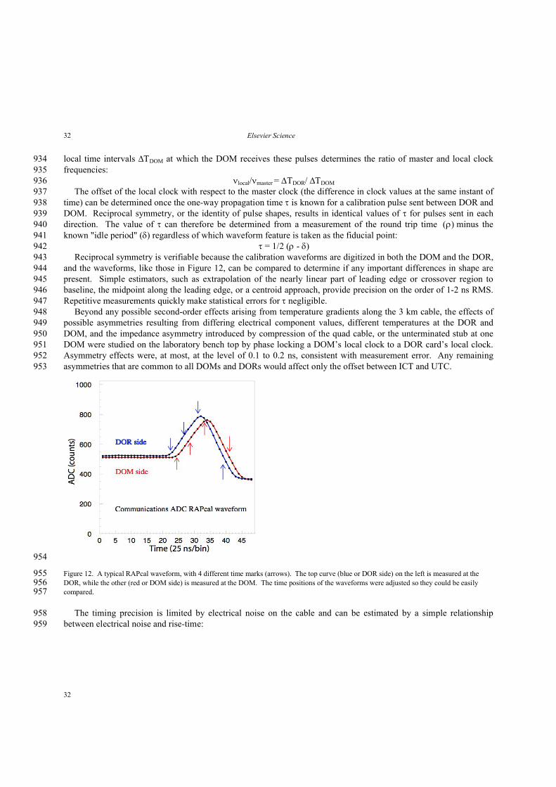
Elsevier Science32
32
local time intervals DOM at which the DOM receives these pulses determines the ratio of master and local clock 934frequencies: 935
local/master = TDOR/DOM936The offset of the local clock with respect to the master clock (the difference in clock values at the same instant of 937
time) can be determined once the one-way propagation time is known for a calibration pulse sent between DOR and 938DOM. Reciprocal symmetry, or the identity of pulse shapes, results in identical values of for pulses sent in each 939direction. The value of can therefore be determined from a measurement of the round trip time minus the 940known "idle period" () regardless of which waveform feature is taken as the fiducial point:941
= 1/2 (- 942Reciprocal symmetry is verifiable because the calibration waveforms are digitized in both the DOM and the DOR, 943
and the waveforms, like those in Figure 12, can be compared to determine if any important differences in shape are 944present. Simple estimators, such as extrapolation of the nearly linear part of leading edge or crossover region to 945baseline, the midpoint along the leading edge, or a centroid approach, provide precision on the order of 1-2 ns RMS. 946Repetitive measurements quickly make statistical errors for negligible.947
Beyond any possible second-order effects arising from temperature gradients along the 3 km cable, the effects of 948possible asymmetries resulting from differing electrical component values, different temperatures at the DOR and 949DOM, and the impedance asymmetry introduced by compression of the quad cable, or the unterminated stub at one 950DOM were studied on the laboratory bench top by phase locking a DOM’s local clock to a DOR card’s local clock. 951Asymmetry effects were, at most, at the level of 0.1 to 0.2 ns, consistent with measurement error. Any remaining 952asymmetries that are common to all DOMs and DORs would affect only the offset between ICT and UTC. 953
954
Figure 12. A typical RAPcal waveform, with 4 different time marks (arrows). The top curve (blue or DOR side) on the left is measured at the 955DOR, while the other (red or DOM side) is measured at the DOM. The time positions of the waveforms were adjusted so they could be easily 956compared. 957
The timing precision is limited by electrical noise on the cable and can be estimated by a simple relationship 958between electrical noise and rise-time: 959
Elsevier Science 33
33
t ~ V/(dV/dt),960where V is the RMS noise/error voltage, and dV/dt is the received pulse rise time, ~ 160 mV/ 0.6 s. From the 961observed timing precision and pulse rise-time, the inferred noise voltage is ~ 0.7 mV, which is slightly higher then 962the communications ADC quantization error of 0.4 mV. Because RAPcal is intrinsically sensitive to high frequency 963electrical noise, care was taken in the design of circuitry, cables, and operation to minimize induced noise. Since the 964time calibration procedure is repeated at regular intervals, individual calibrations that have been substantially affected 965by noise are easily recognized and discarded. In that case, the previous calibration is used for an additional 966calibration interval.967
The RAPcal interrogation rate needed to track the oscillator drift in each DOM depends on the actual stability, 968which is expected to vary somewhat for each oscillator. Typically, the measured DOM oscillator drift under stable 969temperature conditions is remarkably good, with f/f < 3 10-11. This permits interrogation intervals of a minute, or 970perhaps more, before drift has accumulated to a magnitude that would affect off-line event reconstruction. However, 971intrinsic oscillator frequency drifts and phase fluctuations display occasional, minute, abrupt discontinuities. In 972current practice, the time calibration sequence takes less than ~1.4 ms, and is set to occur once per second. The time 973spent in time calibration is hence invisible to the main task of data flow. 974
The coarse timestamp (cf. Section 4.3) is useful for triggering purposes, and is corrected by extrapolation, i.e., by 975using the two previous RAPcal events. In subsequent data analysis, it is possible to use the events just before and just 976after the photon's arrival, i.e., by interpolation. At this time, this correction is not needed as the current method 977provides sufficient precision.978
The ice surrounding the DOMs constitutes a massive, stable heat sink for their crystal oscillators. However, on 979power-up after an extended off period, the oscillators are subject to a ~10C temperature rise due to heating from the 9803.5W dissipated by DOM MB electronics and the PMT HV power supply module within the glass sphere enclosure. 981Once in steady-state operation, the ensemble of all oscillators in IceCube constitutes a very stable virtual clock, 982whose stability is expected to exceed by a wide margin the short- and medium-term stability of the GPS receiver, 983which is affected by algorithmic discontinuities and an evolving mix of satellite signals.984
RAPcal requires distribution to the DOMHubs of GPS-derived signals with sub-nanosecond synchronization, and 985highly coordinated actions in both DOM and DOMHub. The real-time nature of the RAPcal process dictates that 986code is implemented in firmware, rather than software. The RAPcal data set, acquired repetitively, is sufficient to 987establish a rolling time transformation of DOM time to ICT.988
5. DOM MB Manufacturing and Testing Procedures989
Because a deployed DOM cannot be repaired, stringent manufacturing and testing procedures were obligatory to 990minimize failure of a DOM MB during deployment and after it becomes frozen in the ice. The design goal is that not 991more than 5% of the DOMs shall fail within 10 years of operation, where failure is defined as complete loss of 992physics-useful data. A quality control program was developed to support the achievement of this goal. The design 993strategy centered on understanding how, where and why failures occur in boards and associated components when 994exposed to the operational conditions encountered in IceCube. A flow chart describing the production of the DOM 995MB can be seen in Figure 13.996
The design and fabrication philosophy addressed failure propagation, supplier selection, manufacturing quality 997level, material restrictions, design control, and configuration control. The power and communications input circuit 998on the DOM MB is designed to maximize the probability of an open circuit (rather than a short or low-impedance 999circuit) in the event of a catastrophic board failure. This enables the neighboring DOM on the same wire pair to 1000
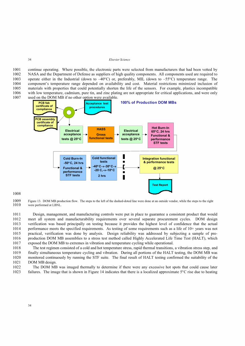
Elsevier Science34
34
continue operating. Where possible, the electronic parts were selected from manufacturers that had been vetted by 1001NASA and the Department of Defense as suppliers of high quality components. All components used are required to1002operate either in the Industrial (down to –40C) or, preferably, MIL (down to –55C) temperature range. The 1003component’s temperature range depended on availability and cost. Material restrictions minimized inclusion of 1004materials with properties that could potentially shorten the life of the sensors. For example, plastics incompatible 1005with low temperature, cadmium, pure tin, and zinc plating are not appropriate for critical applications, and were only 1006used on the DOM MB if no other option were available.1007
100% of Production DOM MBs
Hot Burn-In65C, 24 hrsFunctional &performance
STF tests
Integration functional & performance tests
@ 25C
PCB fabcertificate ofcompliance
PCB assemblycertificate ofcompliance
Cold Burn-In
-50C, 24 hrs
Acceptance testprocedures
HASS
Grossfunctional tests
Electrical acceptance
tests @ 25C
Test Report
Electrical acceptance
tests @ 25C
Cold functional tests
2 hrs
-40C-30C-20 C, -10C
Functional &performance
STF tests
1008
Figure 13. DOM MB production flow. The steps to the left of the dashed-doted line were done at an outside vendor, while the steps to the right 1009were performed at LBNL.1010
Design, management, and manufacturing controls were put in place to guarantee a consistent product that would 1011meet all system and manufacturability requirements over several separate procurement cycles. DOM design 1012verification was based principally on testing because it provides the highest level of confidence that the actual 1013performance meets the specified requirements. As testing of some requirements such as a life of 10+ years was not 1014practical, verification was done by analysis. Design reliability was addressed by subjecting a sample of pre-1015production DOM MB assemblies to a stress test method called Highly Accelerated Life Time Test (HALT), which 1016exposed the DOM MB to extremes in vibration and temperature cycling while operational.1017
The test regimen consisted of a cold and hot temperature stress, rapid thermal transitions, a vibration stress step, and 1018finally simultaneous temperature cycling and vibration. During all portions of the HALT testing, the DOM MB was 1019monitored continuously by running the STF suite. The final result of HALT testing confirmed the suitability of the 1020DOM MB design. 1021
The DOM MB was imaged thermally to determine if there were any excessive hot spots that could cause later 1022failures. The image that is shown in Figure 14 indicates that there is a localized approximate 5C rise due to heating 1023
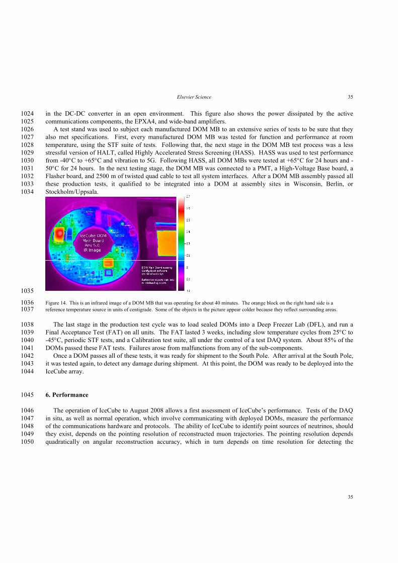
Elsevier Science 35
35
in the DC-DC converter in an open environment. This figure also shows the power dissipated by the active 1024communications components, the EPXA4, and wide-band amplifiers.1025
A test stand was used to subject each manufactured DOM MB to an extensive series of tests to be sure that they 1026also met specifications. First, every manufactured DOM MB was tested for function and performance at room 1027temperature, using the STF suite of tests. Following that, the next stage in the DOM MB test process was a less 1028stressful version of HALT, called Highly Accelerated Stress Screening (HASS). HASS was used to test performance 1029from -40C to +65C and vibration to 5G. Following HASS, all DOM MBs were tested at +65C for 24 hours and -103050C for 24 hours. In the next testing stage, the DOM MB was connected to a PMT, a High-Voltage Base board, a 1031Flasher board, and 2500 m of twisted quad cable to test all system interfaces. After a DOM MB assembly passed all 1032these production tests, it qualified to be integrated into a DOM at assembly sites in Wisconsin, Berlin, or 1033Stockholm/Uppsala.1034
1035
Figure 14. This is an infrared image of a DOM MB that was operating for about 40 minutes. The orange block on the right hand side is a 1036reference temperature source in units of centigrade. Some of the objects in the picture appear colder because they reflect surrounding areas.1037
The last stage in the production test cycle was to load sealed DOMs into a Deep Freezer Lab (DFL), and run a 1038Final Acceptance Test (FAT) on all units. The FAT lasted 3 weeks, including slow temperature cycles from 25C to 1039-45C, periodic STF tests, and a Calibration test suite, all under the control of a test DAQ system. About 85% of the 1040DOMs passed these FAT tests. Failures arose from malfunctions from any of the sub-components.1041
Once a DOM passes all of these tests, it was ready for shipment to the South Pole. After arrival at the South Pole, 1042it was tested again, to detect any damage during shipment. At this point, the DOM was ready to be deployed into the 1043IceCube array.1044
6. Performance1045
The operation of IceCube to August 2008 allows a first assessment of IceCube’s performance. Tests of the DAQ 1046in situ, as well as normal operation, which involve communicating with deployed DOMs, measure the performance 1047of the communications hardware and protocols. The ability of IceCube to identify point sources of neutrinos, should 1048they exist, depends on the pointing resolution of reconstructed muon trajectories. The pointing resolution depends 1049quadratically on angular reconstruction accuracy, which in turn depends on time resolution for detecting the 1050
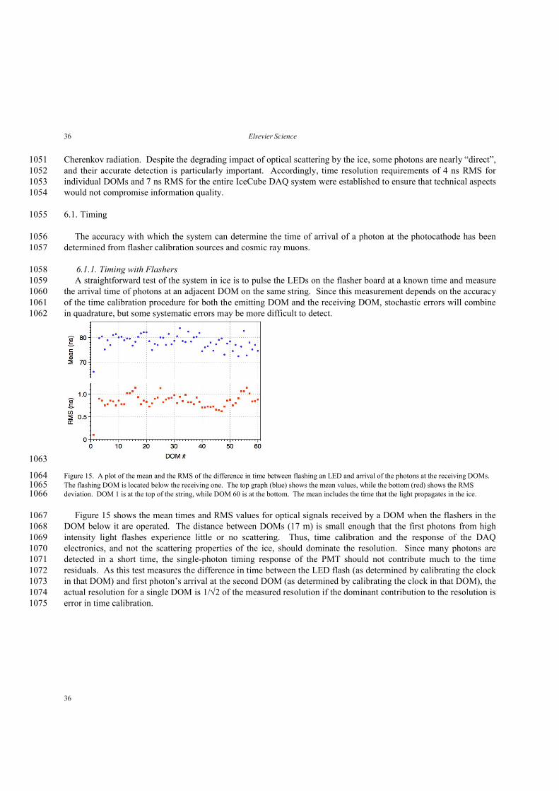
Elsevier Science36
36
Cherenkov radiation. Despite the degrading impact of optical scattering by the ice, some photons are nearly “direct”, 1051and their accurate detection is particularly important. Accordingly, time resolution requirements of 4 ns RMS for 1052individual DOMs and 7 ns RMS for the entire IceCube DAQ system were established to ensure that technical aspects 1053would not compromise information quality. 1054
6.1. Timing1055
The accuracy with which the system can determine the time of arrival of a photon at the photocathode has been 1056determined from flasher calibration sources and cosmic ray muons. 1057
6.1.1. Timing with Flashers1058A straightforward test of the system in ice is to pulse the LEDs on the flasher board at a known time and measure 1059
the arrival time of photons at an adjacent DOM on the same string. Since this measurement depends on the accuracy 1060of the time calibration procedure for both the emitting DOM and the receiving DOM, stochastic errors will combine 1061in quadrature, but some systematic errors may be more difficult to detect.1062
1063
Figure 15. A plot of the mean and the RMS of the difference in time between flashing an LED and arrival of the photons at the receiving DOMs. 1064The flashing DOM is located below the receiving one. The top graph (blue) shows the mean values, while the bottom (red) shows the RMS 1065deviation. DOM 1 is at the top of the string, while DOM 60 is at the bottom. The mean includes the time that the light propagates in the ice.1066
Figure 15 shows the mean times and RMS values for optical signals received by a DOM when the flashers in the 1067DOM below it are operated. The distance between DOMs (17 m) is small enough that the first photons from high 1068intensity light flashes experience little or no scattering. Thus, time calibration and the response of the DAQ 1069electronics, and not the scattering properties of the ice, should dominate the resolution. Since many photons are 1070detected in a short time, the single-photon timing response of the PMT should not contribute much to the time 1071residuals. As this test measures the difference in time between the LED flash (as determined by calibrating the clock 1072in that DOM) and first photon’s arrival at the second DOM (as determined by calibrating the clock in that DOM), the 1073actual resolution for a single DOM is 1/2 of the measured resolution if the dominant contribution to the resolution is 1074error in time calibration.1075
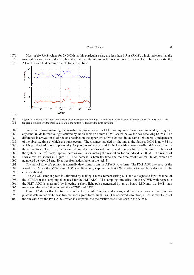
Elsevier Science 37
37
Most of the RMS values for 59 DOMs in this particular string are less than 1.5 ns (RMS), which indicates that the 1076time calibration error and any other stochastic contributions to the resolution are 1 ns or less. In these tests, the 1077ATWD is used to determine the photon arrival time.1078
1079
Figure 16. The RMS and mean time difference between photons arriving at two adjacent DOMs located just above a third, flashing DOM. The 1080top graph (blue) shows the mean values, while the bottom (red) shows the RMS deviation.1081
Systematic errors in timing that involve the properties of the LED flashing system can be eliminated by using two 1082adjacent DOMs to receive light emitted by the flashers on a third DOM located below the two receiving DOMs. The 1083difference in arrival times of photons received in the upper two DOMs emitted in the same light burst is independent 1084of the absolute time at which the burst occurs. The distance traveled by photons to the farthest DOM is now 34 m, 1085which provides additional opportunity for photons to be scattered in the ice with a corresponding delay and jitter in 1086the arrival time. Therefore, the measured time distributions will correspond to upper limits on the time resolution of 1087the system. A 1/√2 factor applies here as well in estimating the resolution for an individual DOM. The results of 1088such a test are shown in Figure 16. The increase in both the time and the time resolution for DOMs, which are 1089numbered between 33 and 40, arises from a dust layer in the ice[13].1090
The arrival time of a photon is normally determined from the ATWD waveform. The PMT ADC also records the 1091waveform. Since the ATWD and ADC simultaneously capture the first 420 ns after a trigger, both devices can be 1092cross calibrated.1093
The ATWD sampling rate is calibrated by making a measurement (using STF and a diagnostic input channel of 1094the ATWD) of the sampling clock used for the PMT ADC. The sampling time offset for the ATWD with respect to 1095the PMT ADC is measured by injecting a short light pulse generated by an on-board LED into the PMT, then 1096measuring the arrival time in both the ATWD and ADC.1097
Figure 17 shows that the time resolution for the ADC is just under 5 ns, and that the average arrival time for 1098photons determined with these two methods agrees to within 0.6 ns. The observed resolution, 4.7 ns, is about 20% of 1099the bin width for the PMT ADC, which is comparable to the relative resolution seen in the ATWD. 1100
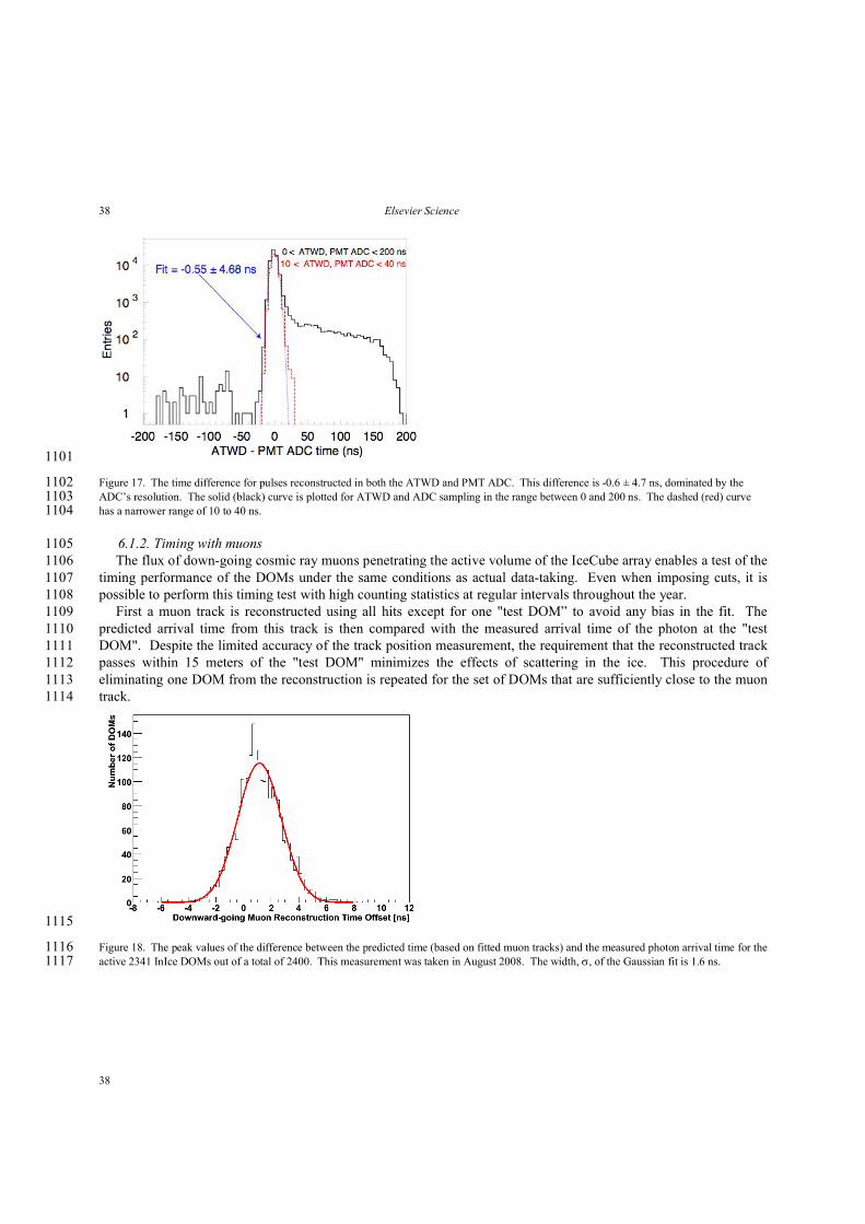
Elsevier Science38
38
1101
Figure 17. The time difference for pulses reconstructed in both the ATWD and PMT ADC. This difference is -0.6 ± 4.7 ns, dominated by the 1102ADC’s resolution. The solid (black) curve is plotted for ATWD and ADC sampling in the range between 0 and 200 ns. The dashed (red) curve 1103has a narrower range of 10 to 40 ns.1104
6.1.2. Timing with muons1105The flux of down-going cosmic ray muons penetrating the active volume of the IceCube array enables a test of the 1106
timing performance of the DOMs under the same conditions as actual data-taking. Even when imposing cuts, it is 1107possible to perform this timing test with high counting statistics at regular intervals throughout the year.1108
First a muon track is reconstructed using all hits except for one "test DOM” to avoid any bias in the fit. The 1109predicted arrival time from this track is then compared with the measured arrival time of the photon at the "test 1110DOM". Despite the limited accuracy of the track position measurement, the requirement that the reconstructed track 1111passes within 15 meters of the "test DOM" minimizes the effects of scattering in the ice. This procedure of 1112eliminating one DOM from the reconstruction is repeated for the set of DOMs that are sufficiently close to the muon 1113track.1114
1115
Figure 18. The peak values of the difference between the predicted time (based on fitted muon tracks) and the measured photon arrival time for the 1116active 2341 InIce DOMs out of a total of 2400. This measurement was taken in August 2008. The width, , of the Gaussian fit is 1.6 ns. 1117
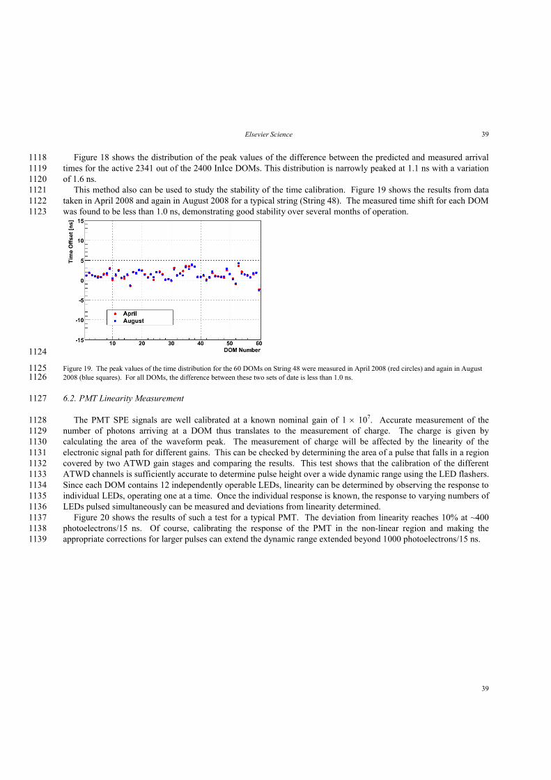
Elsevier Science 39
39
Figure 18 shows the distribution of the peak values of the difference between the predicted and measured arrival 1118times for the active 2341 out of the 2400 InIce DOMs. This distribution is narrowly peaked at 1.1 ns with a variation 1119of 1.6 ns.1120
This method also can be used to study the stability of the time calibration. Figure 19 shows the results from data 1121taken in April 2008 and again in August 2008 for a typical string (String 48). The measured time shift for each DOM 1122was found to be less than 1.0 ns, demonstrating good stability over several months of operation.1123
1124
Figure 19. The peak values of the time distribution for the 60 DOMs on String 48 were measured in April 2008 (red circles) and again in August 11252008 (blue squares). For all DOMs, the difference between these two sets of date is less than 1.0 ns.1126
6.2. PMT Linearity Measurement1127
The PMT SPE signals are well calibrated at a known nominal gain of 1 107. Accurate measurement of the 1128number of photons arriving at a DOM thus translates to the measurement of charge. The charge is given by 1129calculating the area of the waveform peak. The measurement of charge will be affected by the linearity of the 1130electronic signal path for different gains. This can be checked by determining the area of a pulse that falls in a region 1131covered by two ATWD gain stages and comparing the results. This test shows that the calibration of the different 1132ATWD channels is sufficiently accurate to determine pulse height over a wide dynamic range using the LED flashers. 1133Since each DOM contains 12 independently operable LEDs, linearity can be determined by observing the response to 1134individual LEDs, operating one at a time. Once the individual response is known, the response to varying numbers of 1135LEDs pulsed simultaneously can be measured and deviations from linearity determined.1136
Figure 20 shows the results of such a test for a typical PMT. The deviation from linearity reaches 10% at ~400 1137photoelectrons/15 ns. Of course, calibrating the response of the PMT in the non-linear region and making the 1138appropriate corrections for larger pulses can extend the dynamic range extended beyond 1000 photoelectrons/15 ns.1139
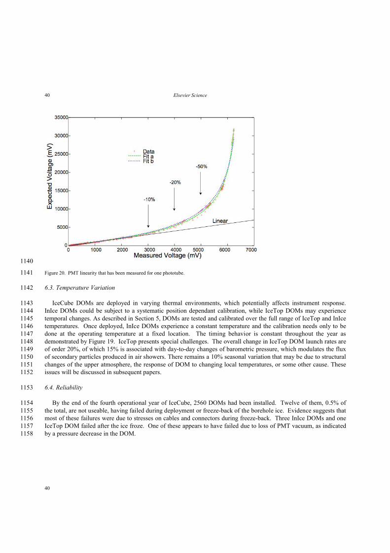
Elsevier Science40
40
1140
Figure 20. PMT linearity that has been measured for one phototube.1141
6.3. Temperature Variation1142
IceCube DOMs are deployed in varying thermal environments, which potentially affects instrument response. 1143InIce DOMs could be subject to a systematic position dependant calibration, while IceTop DOMs may experience 1144temporal changes. As described in Section 5, DOMs are tested and calibrated over the full range of IceTop and InIce 1145temperatures. Once deployed, InIce DOMs experience a constant temperature and the calibration needs only to be 1146done at the operating temperature at a fixed location. The timing behavior is constant throughout the year as 1147demonstrated by Figure 19. IceTop presents special challenges. The overall change in IceTop DOM launch rates are 1148of order 20%, of which 15% is associated with day-to-day changes of barometric pressure, which modulates the flux 1149of secondary particles produced in air showers. There remains a 10% seasonal variation that may be due to structural 1150changes of the upper atmosphere, the response of DOM to changing local temperatures, or some other cause. These 1151issues will be discussed in subsequent papers.1152
6.4. Reliability1153
By the end of the fourth operational year of IceCube, 2560 DOMs had been installed. Twelve of them, 0.5% of 1154the total, are not useable, having failed during deployment or freeze-back of the borehole ice. Evidence suggests that 1155most of these failures were due to stresses on cables and connectors during freeze-back. Three InIce DOMs and one 1156IceTop DOM failed after the ice froze. One of these appears to have failed due to loss of PMT vacuum, as indicated 1157by a pressure decrease in the DOM.1158
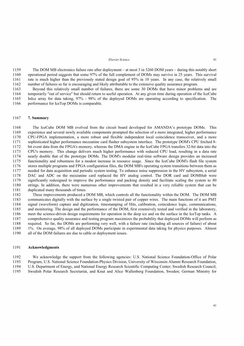
Elsevier Science 41
41
The DOM MB electronics failure rate after deployment – at most 3 in 3260 DOM years – during this notably short 1159operational period suggests that some 97% of the full complement of DOMs may survive in 25 years. This survival 1160rate is much higher than the previously stated design goal of 95% in 10 years. In any case, the relatively small 1161number of failures so far is encouraging and likely attributable to the extensive quality assurance program.1162
Beyond this relatively small number of failures, there are some 30 DOMs that have minor problems and are 1163temporarily "out of service" but should return to useful operation. At any given time during operation of the IceCube 1164InIce array for data taking, 97% - 98% of the deployed DOMs are operating according to specification. The 1165performance for IceTop DOMs is comparable.1166
7. Summary1167
The IceCube DOM MB evolved from the circuit board developed for AMANDA’s prototype DOMs. This 1168experience and several newly available components prompted the selection of a more integrated, higher performance 1169CPU-FPGA implementation, a more robust and flexible independent local coincidence transceiver, and a more 1170sophisticated higher performance mezzanine card flasher subsystem interface. The prototype DOM's CPU fetched 8-1171bit event data from the FPGA's memory, whereas the DMA engine in the IceCube FPGA transfers 32-bit data into the 1172CPU's memory. This change delivers much higher performance with reduced CPU load, resulting in a data rate 1173nearly double that of the prototype DOMs. The DOM's modular real-time software design provides an increased 1174functionality and robustness for a modest increase in resource usage. Since the IceCube DOM's flash file system 1175stores multiple programs and FPGA configuration files, the DOM MB's operating system transitions between them as 1176needed for data acquisition and periodic system testing. To enhance noise suppression in the HV subsystem, a serial 1177DAC and ADC on the mezzanine card replaced the HV analog control. The DOR card and DOMHub were 1178significantly redesigned to improve the performance and packing density and facilitate scaling the system to 80 1179strings. In addition, there were numerous other improvements that resulted in a very reliable system that can be 1180duplicated many thousands of times.1181
These improvements produced a DOM MB, which controls all the functionality within the DOM. The DOM MB 1182communicates digitally with the surface by a single twisted pair of copper wires. The main functions of it are PMT 1183signal (waveform) capture and digitization, timestamping of Hits, calibration, coincidence logic, communications, 1184and monitoring. The design and the performance of the DOM, first extensively tested and verified in the laboratory, 1185meet the science-driven design requirements for operation in the deep ice and on the surface in the IceTop tanks. A 1186comprehensive quality assurance and testing program maximizes the probability that deployed DOMs will perform as 1187required. So far, the DOMs are performing very well, with a failure rate (including all sources of failure) of about 11881%. On average, 98% of all deployed DOMs participate in experimental data taking for physics purposes. Almost 1189all of the DOM failures are due to cable or deployment issues.1190
Acknowledgments1191
We acknowledge the support from the following agencies: U.S. National Science Foundation-Office of Polar 1192Program, U.S. National Science Foundation-Physics Division, University of Wisconsin Alumni Research Foundation, 1193U.S. Department of Energy, and National Energy Research Scientific Computing Center; Swedish Research Council, 1194Swedish Polar Research Secretariat, and Knut and Alice Wallenberg Foundation, Sweden; German Ministry for 1195
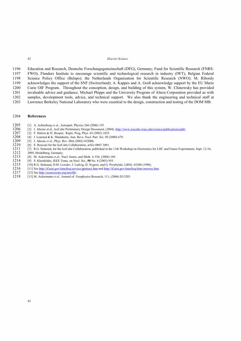
Elsevier Science42
42
Education and Research, Deutsche Forschungsgemeinschaft (DFG), Germany; Fund for Scientific Research (FNRS-1196FWO), Flanders Institute to encourage scientific and technological research in industry (IWT), Belgian Federal 1197Science Policy Office (Belspo); the Netherlands Organisation for Scientific Research (NWO); M. Ribordy 1198acknowledges the support of the SNF (Switzerland); A. Kappes and A. Groß acknowledge support by the EU Marie 1199Curie OIF Program. Throughout the conception, design, and building of this system, W. Chinowsky has provided 1200invaluable advice and guidance. Michael Phipps and the University Program of Altera Corporation provided us with 1201samples, development tools, advice, and technical support. We also thank the engineering and technical staff at 1202Lawrence Berkeley National Laboratory who were essential to the design, construction and testing of the DOM MB.1203
References1204
[1] A. Achterberg et al., Astropart. Physics 266 (2006) 155.1205[2] J. Ahrens et al., IceCube Preliminary Design Document, (2004). http://www.icecube.wisc.edu/science/publications/pdd/.1206[3] F. Halzen & D. Hooper, Repts. Prog, Phys. 65 (2002) 1025.1207[4] J. Learned & K. Mannheim, Ann. Revs. Nucl. Part. Sci. 50 (2000) 679.1208[5] J. Ahrens et al., Phys. Rev. D66 (2002) 032006.1209[6] E. Resconi for the IceCube Collaboration, arXiv:0807.3891.1210[7] R.G. Stokstad, for the IceCube Collaboration, published in the 11th Workshop on Electronics for LHC and Future Experiments, Sept. 12-16, 12112005, Heidelberg, Germany.1212[8] M. Ackermann et al., Nucl. Instru. and Meth. A 556, (2006) 169.1213[9] S. Kleinfelder, IEEE Trans. on Nucl. Sci., 50 No. 4 (2003) 955.1214[10] R.G. Stokstad, D.M. Lowder, J. Ludvig, D. Nygren, and G. Przybylski, LBNL-43200 (1998).1215[11] See http://tf.nist.gov/timefreq/service/gpstrace.htm and http://tf.nist.gov/timefreq/time/oneway.htm.1216[12] See http://sourceware.org/newlib/.1217[13] M. Ackermann et al., Journal of Geophysics Research, 111, (2006) D13203. 1218
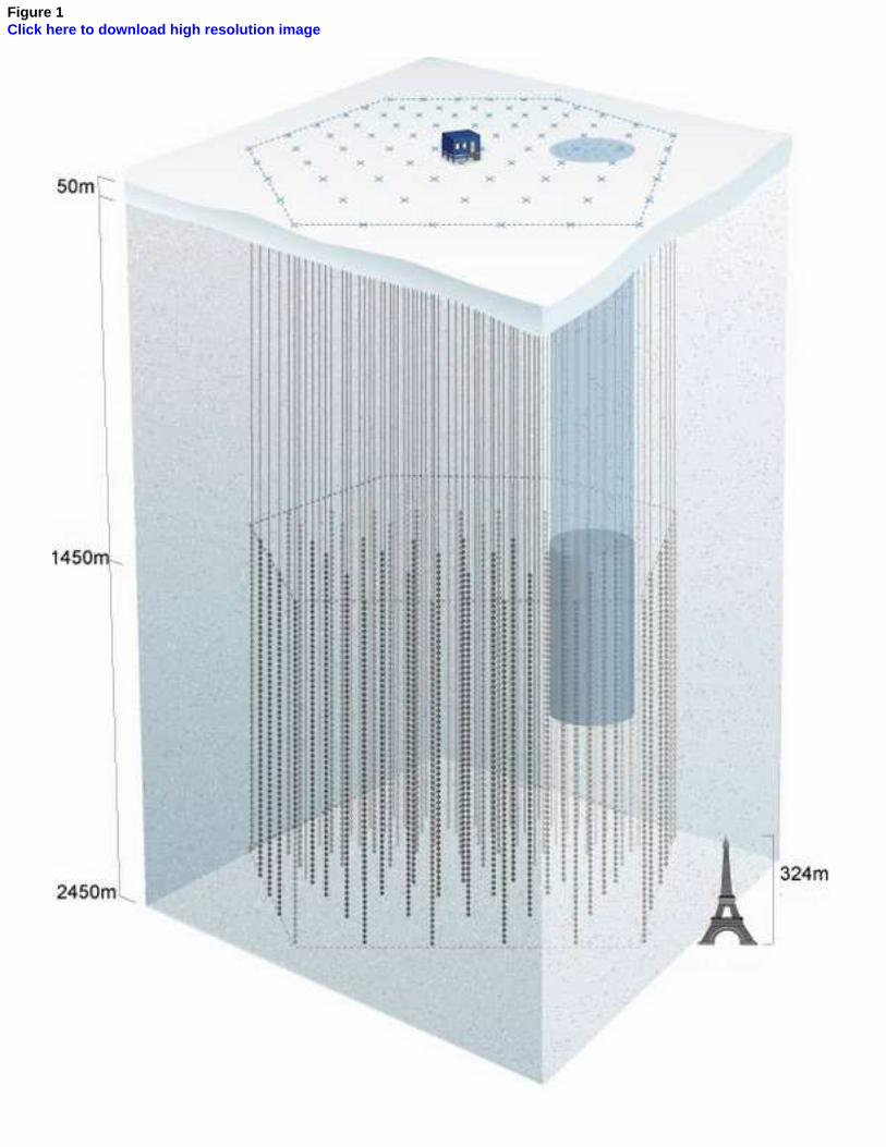
Figure 1Click here to download high resolution image
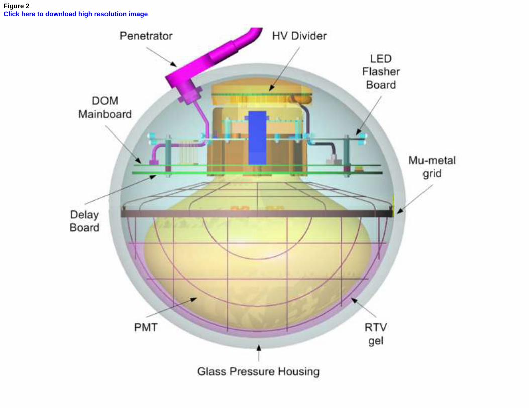
Figure 2Click here to download high resolution image
Figure 3Click here to download high resolution image
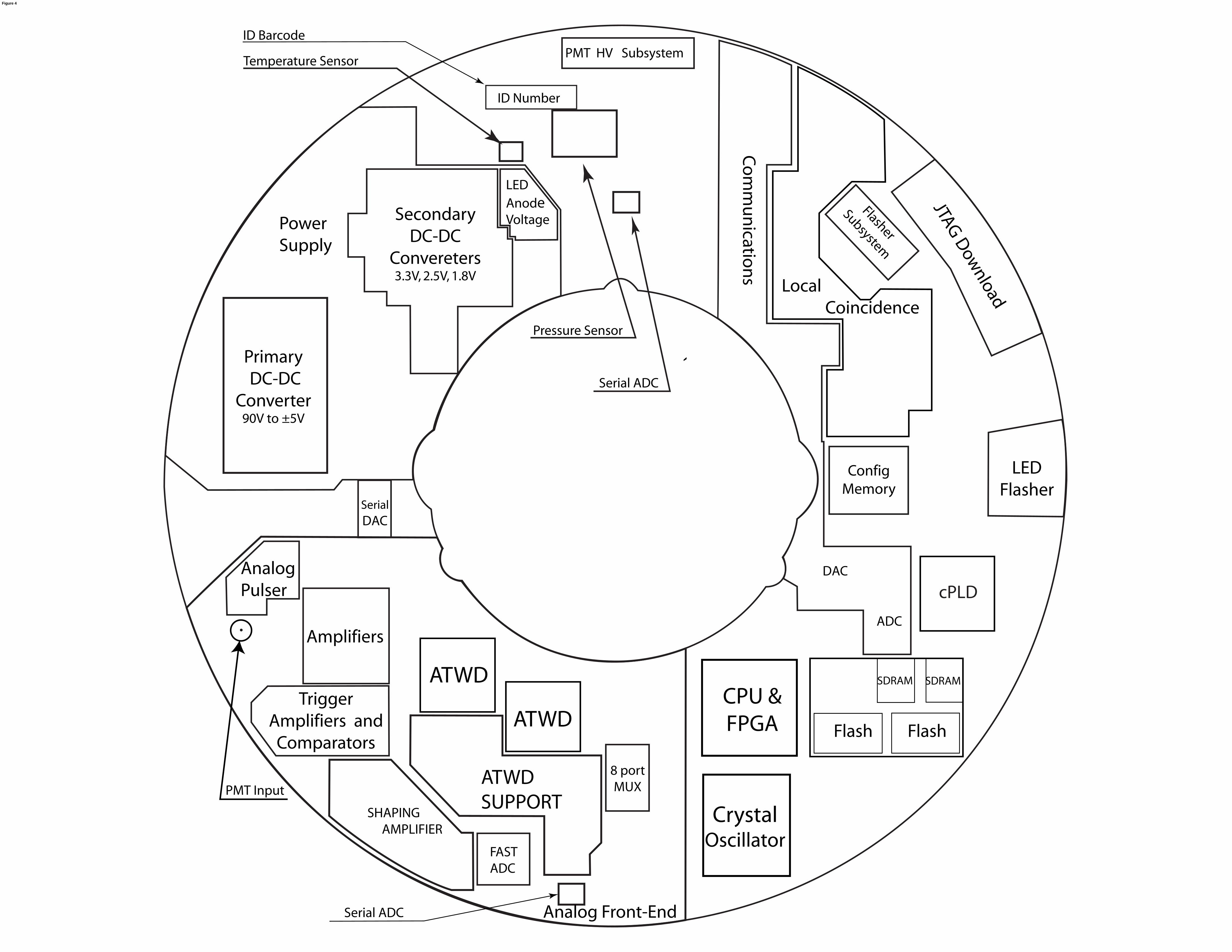
ID Barcode
SecondaryDC-DC
Convereters3.3V, 2.5V, 1.8V
CPU &FPGA
CrystalOscillator
SDRAM
Primary DC-DC
Converter90V to ±5V
cPLD
ATWD
ATWD
Amplifiers
AnalogPulser
TriggerAmplifiers and
Comparators
SHAPING AMPLIFIER
ATWDSUPPORT
FASTADC
8 portMUX
Flash Flash
Local Coincidence
Comm
unications
JTAG Dow
nload
LEDFlasher
ConfigMemory
PMT HV Subsystem
Flasher
Subsystem
ADC
DAC
Pressure Sensor
Analog Front-End
PowerSupply
LEDAnodeVoltage
SerialDAC
ID Number
PMT Input
SDRAM
`
Temperature Sensor
Serial ADC
Serial ADC
Figure 4
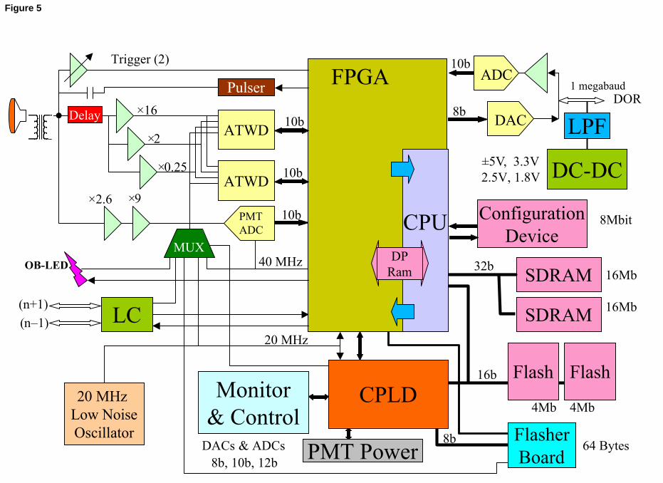
FPGA
CPU
CPLDFlash Flash
PMT Power
SDRAM
SDRAM
ATWD
ATWD
DAC
Monitor& Control
LPF
LC
×16
×2
×0.25
FlasherBoard
Pulser
DACs & ADCs
4Mb 4Mb
16Mb
16Mb
3.3V 2.5V, 1.8V
64 Bytes
Trigger (2)ADC
20 MHz Low NoiseOscillator
20 MHz
40 MHzMUX
(n+1)(n–1)
DOR
OB-LED
×2.6 ×9
10b
10b
10b
10b
8b
32b
16b
8b
8b, 10b, 12b
DPRam
1 megabaud
DC-DC
ConfigurationDevice
8Mbit
Delay
±5V,
PMTADC
Figure 5
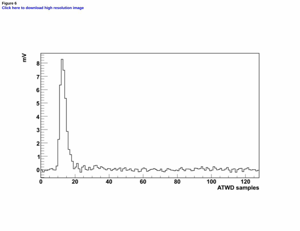
Figure 6Click here to download high resolution image
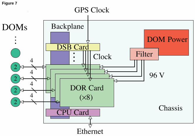
FilterDSB Card
2
2
2
2
…DOMs
DOM Power
DOR Cards
Backplane
96 VDOR Card
(×8)
… Clock
Chassis
GPS Clock
CPU Card
Ethernet
4
4
4
4
Figure 7
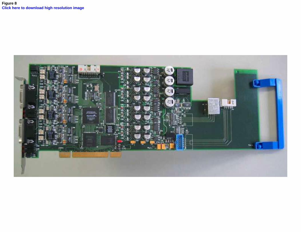
Figure 8Click here to download high resolution image
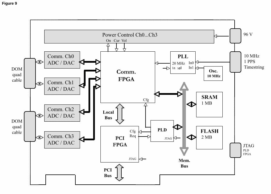
Comm. Ch0ADC / DAC
FLASH2 MB
PLD
Comm.FPGA
PCIBus
96 V
SRAM1 MB
PCIFPGA
LocalBus
Mem.Bus
CfgReq
Cfg
Comm. Ch1ADC / DAC
Comm. Ch2ADC / DAC
Comm. Ch3ADC / DAC
10 MHz1 PPSTimestring
JTAGPLDFPGA
PLLIn0In1
Osc.10 MHz
20 MHz
Power Control Ch0...Ch3On Cur Vol
DOMquadcable
DOMquadcable
JTAG
JTAG
Figure 9
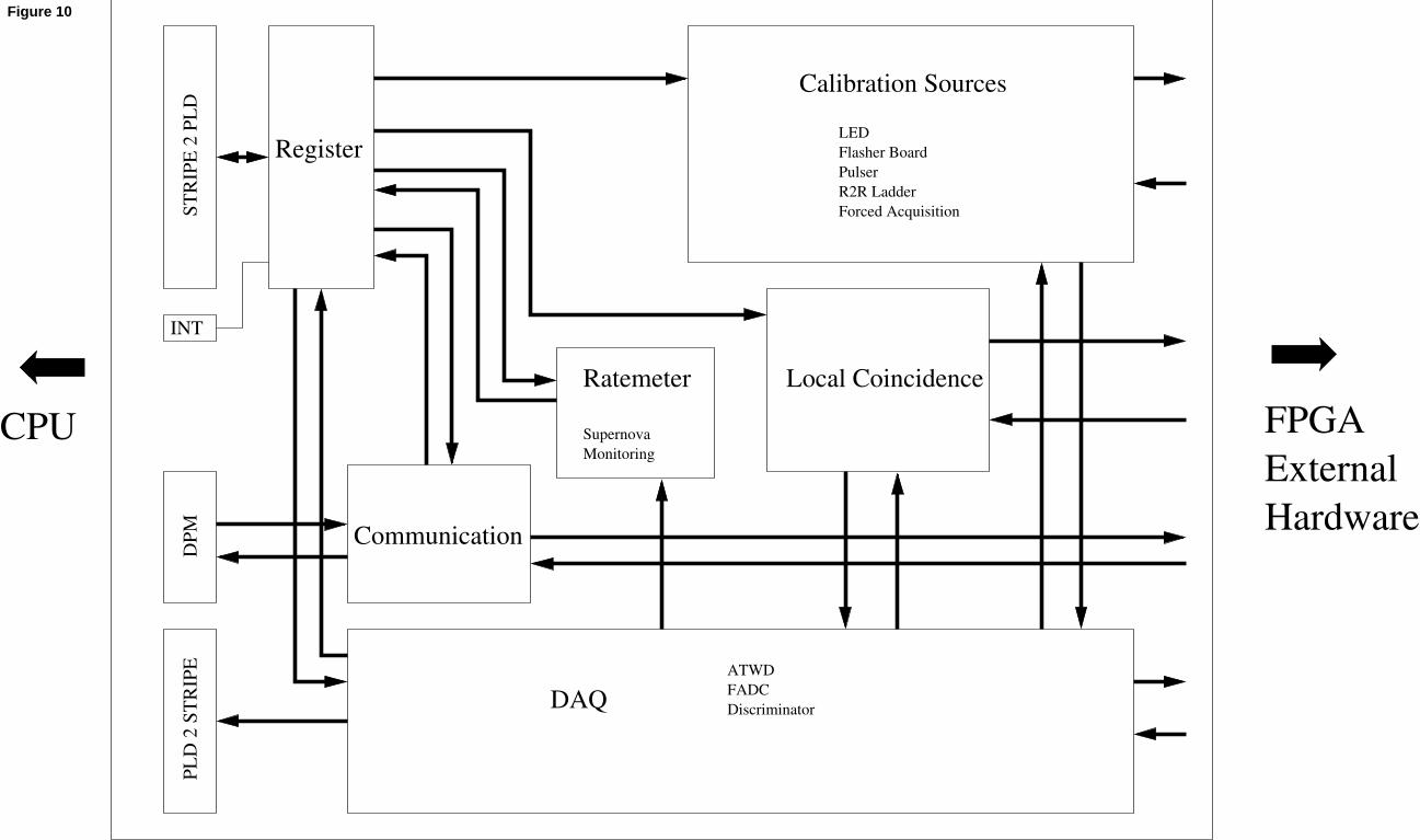
ATWDFADCDiscriminator
LEDFlasher BoardPulserR2R LadderForced Acquisition
ExternalHardware
FPGA
Register
Communication
Local Coincidence
PLD
2 S
TR
IPE
DPM
INT
STR
IPE
2 P
LD
SupernovaMonitoring
Ratemeter
Calibration Sources
DAQ
CPU
Figure 10
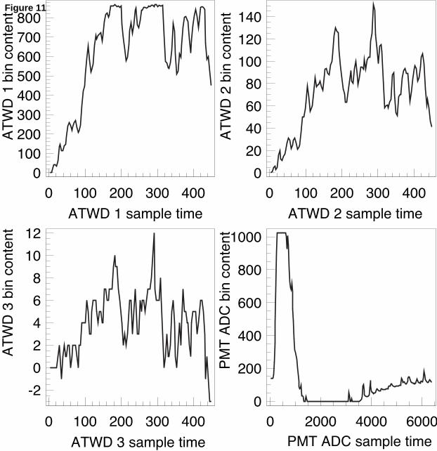
ATWD 1 sample time
ATW
D1
bin
cont
ent
ATWD 2 sample timeAT
WD
2 b
in c
onte
nt
ATWD 3 sample time
ATW
D3
bin
cont
ent
PMT ADC sample time
PMT
ADC
bin
con
tent
0100200300400500600700800
0 100 200 300 4000
20406080
100120140
0 100 200 300 400
-202468
1012
0 100 200 300 4000
200
400
600
800
1000
0 2000 4000 6000
Figure 11
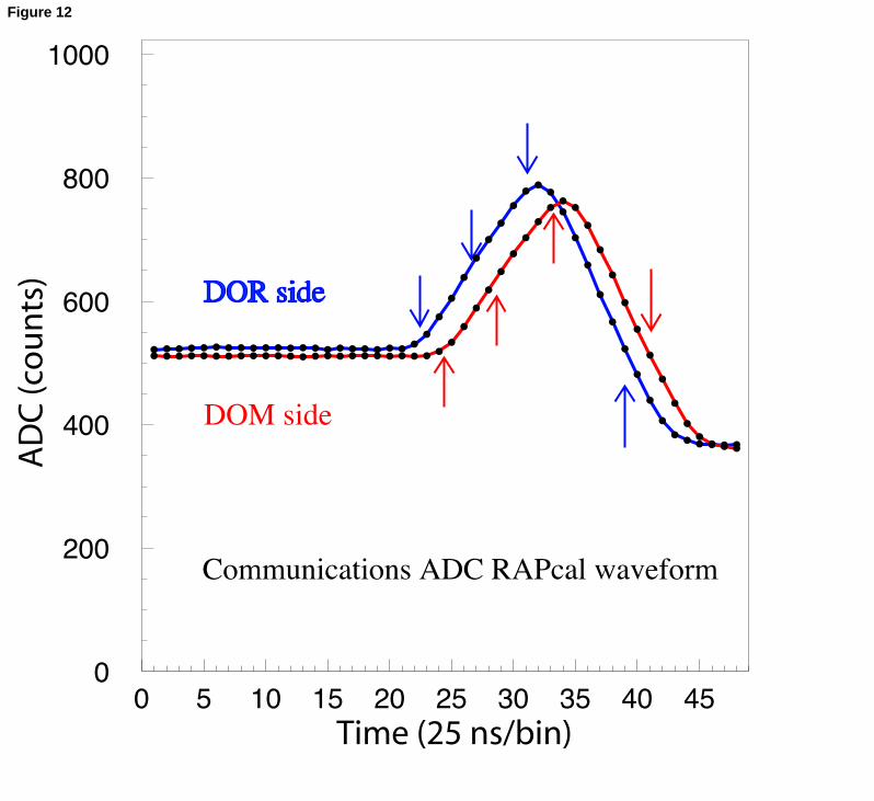
DOR side
DOM side
Communications ADC RAPcal waveform
0
200
400
600
800
1000
0 5 10 15 20 25 30 35 40 45Time (25 ns/bin)
AD
C (c
ou
nts
)Figure 12
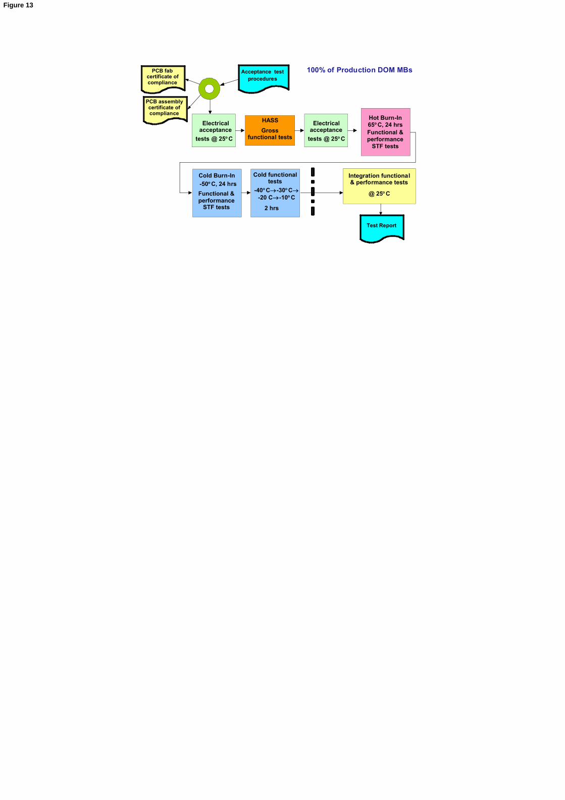
100% of Production DOM MBs
Hot Burn-In65C, 24 hrsFunctional &performance
STF tests
Integration functional & performance tests
@ 25C
PCB fabcertificate ofcompliance
PCB assemblycertificate ofcompliance
Cold Burn-In
-50C, 24 hrs
Acceptance testprocedures
HASS
Grossfunctional tests
Electrical acceptance
tests @ 25C
Test Report
Electrical acceptance
tests @ 25C
Cold functional tests
2 hrs
-40C-30C-20 C-10C
Functional &performance
STF tests
Figure 13
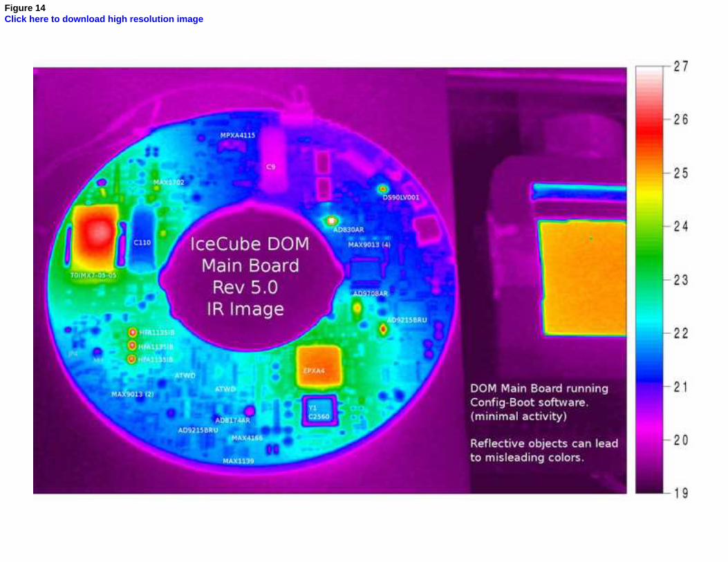
Figure 14Click here to download high resolution image
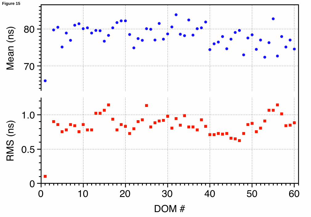
RMS
(ns)
0
0.5
1.0
Mea
n (n
s)
70
80
DOM #0 10 20 30 40 50 60
Figure 15
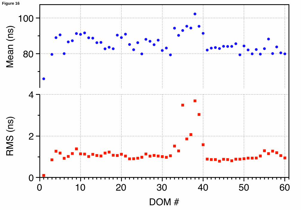
RMS
(ns)
0
2
4
Mea
n (n
s)
80
100
DOM #0 10 20 30 40 50 60
Figure 16
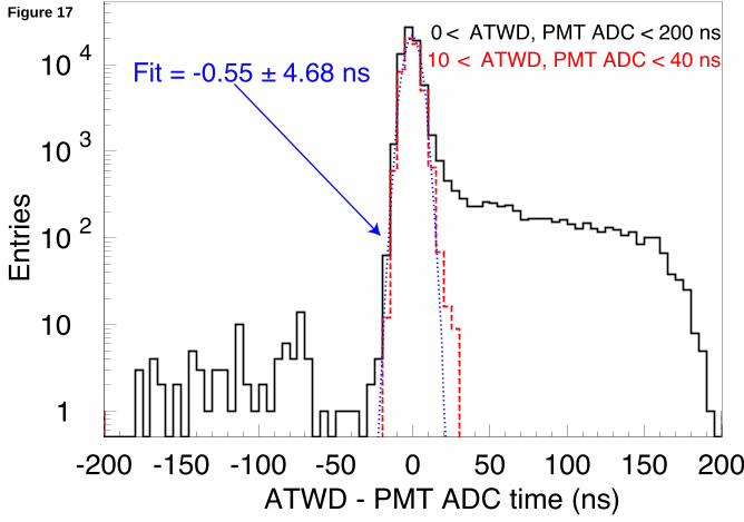
Fit = -0.55 ± 4.68 ns 0 < ATWD, PMT ADC < 200 ns10 < ATWD, PMT ADC < 40 ns
ATWD - PMT ADC time (ns)
Entri
es
1
10
10 2
10 3
10 4
-200 -150 -100 -50 0 50 100 150 200
Figure 17
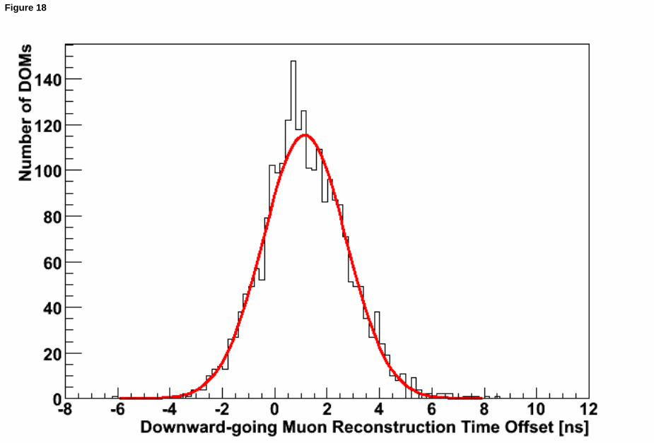
Figure 18
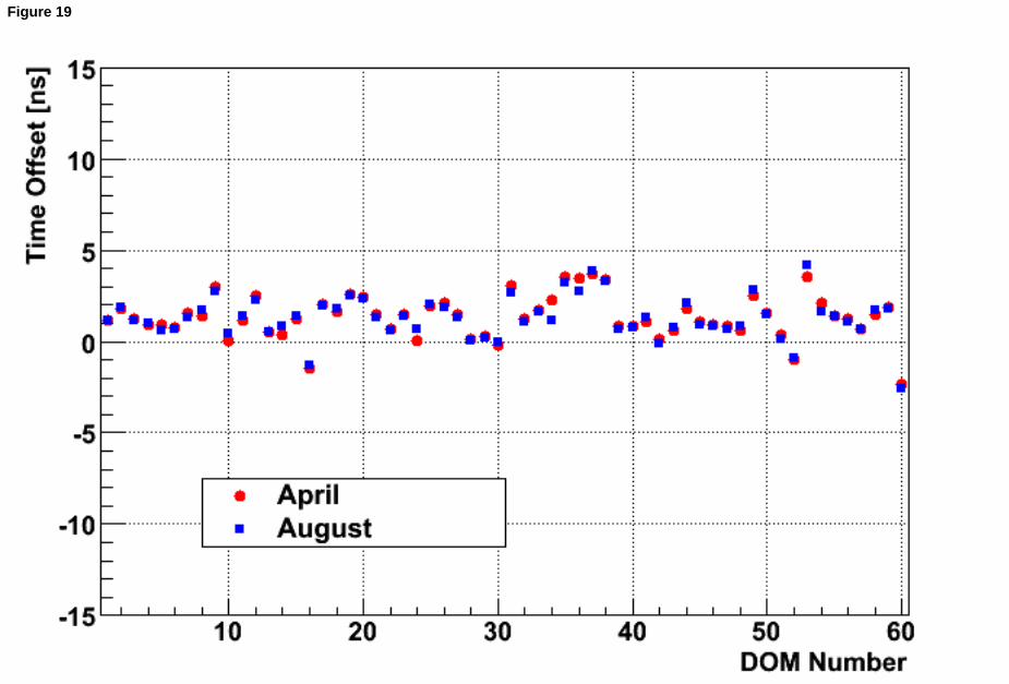
Figure 19
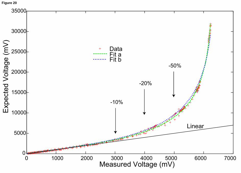
0
5000
10000
15000
20000
25000
30000
35000
0 1000 2000 3000 4000 5000 6000 7000
Exp
ecte
d V
olta
ge (m
V)
Measured Voltage (mV)
DataFit a Fit b
-10%
-20%
-50%
Linear
Figure 20
Related Documents