NANO EXPRESS Open Access The function of a 60-nm-thick AlN buffer layer in n-ZnO/AlN/p-Si(111) Wei Wang, Chao Chen, Guozhen Zhang, Ti Wang, Hao Wu * , Yong Liu and Chang Liu * Abstract ZnO films were prepared on p-Si (111) substrates by using atomic layer deposition. High-resolution x-ray diffraction (XRD), scanning electron microscopy (SEM), x-ray photoelectron spectroscopy (XPS), photoluminescence (PL), and I-V measurements were carried out to characterize structural, electrical, and optical properties. After introducing a 60-nm-thick AlN buffer layer, the growth direction of the ZnO films was changed from [10] to [0002]. Meanwhile, the ZnO crystalline quality was significantly improved as verified by both XRD and PL analyses. It has been demonstrated that the reverse leakage current was greatly reduced with the AlN buffer layer. The valence band offsets have been determined to be 3.06, 2.95, and 0.83 eV for ZnO/Si, ZnO/AlN, and AlN/Si heterojunctions, respectively, and the band alignment of ZnO/Si heterojunction was modified to be 0.72 eV after introducing the AlN buffer layer. Our work offered a potential way to fabricate Si-based ultraviolet light-emitting diodes and improve the device performances. Keywords: AlN buffer layer; Heterojunction; ALD; Band alignment Background Si is the most useful substrate due to its low cost and easy integration [1,2]. P-type Si has the prominent merits to make driving voltage of light-emitting diode (LED) lower and the cost of device less expensive [3]. Therefore, the Si-based LEDs possess great competitive- ness. Zinc oxide (ZnO) is of interest as a result of its po- tential applications in ultraviolet (UV) optoelectronic devices due to its wide band gap of approximately 3.4 eV at room temperature and high exciton binding energy of approximately 60 meV [4]. Moreover, ZnO is thermally and chemically stable in ambient air, highly transparent in the visible region (>85%) [5], resistant to be oxidized, easy to fabricate, and relatively cheap compared to other optoelectronic materials [6]. So far, a variety of tech- niques have been utilized to grow ZnO thin films, such as, sputtering [7], molecular beam epitaxy (MBE) [8], pulsed laser deposition [9], and chemical vapor depos- ition [10]. As a chemical vapor processing with accurate surface control and self-limiting, atomic layer deposition (ALD) can prepare thin films with high uniformities and low defect densities. Because of the large mismatches of the lattice con- stants (15.4%) and thermal expansion coefficients (60%) between ZnO and Si [11] and the oxidation of Si surface, direct growth of ZnO on Si substrates resulted in amorphous or polycrystalline films [12]. Attempts have been made to solve this problem by inserting different buffer layers between ZnO and substrates, such as GaN [13] and Al 2 O 3 [14,15]. It is well know that in the system of n-ZnO/p-Si, electron and hole recombination takes place mainly in Si rather than in ZnO, leading to a diffi- cult application for lighting since Si has a narrow and in- direct band gap. Owing to the difference in band gaps between ZnO and Si that provides an effective electron injection from ZnO to p-Si and blocks the flow of holes from p-Si to ZnO [16], it is necessary to understand the physical properties of the ZnO/Si heterojunction, espe- cially the energy band alignment and interfacial micro- structure. Some researchers employed different dielectric buffer layers to study the band alignment of the ZnO/ p-Si heterojunction [16-18]. However, few reports men- tioned AlN buffer layers between ZnO and Si. AlN has the widest direct band gap (6.2 eV) among all III-nitride * Correspondence: [email protected]; [email protected] Key Laboratory of Artificial Micro- and Nano-structures of Ministry of Education, and School of Physics and Technology, Wuhan University, Wuhan 430072, People’s Republic of China © 2015 Wang et al.; licensee Springer. This is an Open Access article distributed under the terms of the Creative Commons Attribution License (http://creativecommons.org/licenses/by/4.0), which permits unrestricted use, distribution, and reproduction in any medium, provided the original work is properly credited. Wang et al. Nanoscale Research Letters (2015) 10:91 DOI 10.1186/s11671-015-0809-3

Welcome message from author
This document is posted to help you gain knowledge. Please leave a comment to let me know what you think about it! Share it to your friends and learn new things together.
Transcript
Wang et al. Nanoscale Research Letters (2015) 10:91 DOI 10.1186/s11671-015-0809-3
NANO EXPRESS Open Access
The function of a 60-nm-thick AlN buffer layer inn-ZnO/AlN/p-Si(111)Wei Wang, Chao Chen, Guozhen Zhang, Ti Wang, Hao Wu*, Yong Liu and Chang Liu*
Abstract
ZnO films were prepared on p-Si (111) substrates by using atomic layer deposition. High-resolution x-ray diffraction(XRD), scanning electron microscopy (SEM), x-ray photoelectron spectroscopy (XPS), photoluminescence (PL), andI-V measurements were carried out to characterize structural, electrical, and optical properties. After introducing a60-nm-thick AlN buffer layer, the growth direction of the ZnO films was changed from [10] to [0002]. Meanwhile, theZnO crystalline quality was significantly improved as verified by both XRD and PL analyses. It has been demonstratedthat the reverse leakage current was greatly reduced with the AlN buffer layer. The valence band offsets have beendetermined to be 3.06, 2.95, and 0.83 eV for ZnO/Si, ZnO/AlN, and AlN/Si heterojunctions, respectively, and the bandalignment of ZnO/Si heterojunction was modified to be 0.72 eV after introducing the AlN buffer layer. Our work offereda potential way to fabricate Si-based ultraviolet light-emitting diodes and improve the device performances.
Keywords: AlN buffer layer; Heterojunction; ALD; Band alignment
BackgroundSi is the most useful substrate due to its low cost andeasy integration [1,2]. P-type Si has the prominentmerits to make driving voltage of light-emitting diode(LED) lower and the cost of device less expensive [3].Therefore, the Si-based LEDs possess great competitive-ness. Zinc oxide (ZnO) is of interest as a result of its po-tential applications in ultraviolet (UV) optoelectronicdevices due to its wide band gap of approximately 3.4 eVat room temperature and high exciton binding energy ofapproximately 60 meV [4]. Moreover, ZnO is thermallyand chemically stable in ambient air, highly transparentin the visible region (>85%) [5], resistant to be oxidized,easy to fabricate, and relatively cheap compared to otheroptoelectronic materials [6]. So far, a variety of tech-niques have been utilized to grow ZnO thin films, suchas, sputtering [7], molecular beam epitaxy (MBE) [8],pulsed laser deposition [9], and chemical vapor depos-ition [10]. As a chemical vapor processing with accuratesurface control and self-limiting, atomic layer deposition(ALD) can prepare thin films with high uniformities andlow defect densities.
* Correspondence: [email protected]; [email protected] Laboratory of Artificial Micro- and Nano-structures of Ministry ofEducation, and School of Physics and Technology, Wuhan University, Wuhan430072, People’s Republic of China
© 2015 Wang et al.; licensee Springer. This is aAttribution License (http://creativecommons.orin any medium, provided the original work is p
Because of the large mismatches of the lattice con-stants (15.4%) and thermal expansion coefficients (60%)between ZnO and Si [11] and the oxidation of Si surface,direct growth of ZnO on Si substrates resulted inamorphous or polycrystalline films [12]. Attempts havebeen made to solve this problem by inserting differentbuffer layers between ZnO and substrates, such as GaN[13] and Al2O3 [14,15]. It is well know that in the systemof n-ZnO/p-Si, electron and hole recombination takesplace mainly in Si rather than in ZnO, leading to a diffi-cult application for lighting since Si has a narrow and in-direct band gap. Owing to the difference in band gapsbetween ZnO and Si that provides an effective electroninjection from ZnO to p-Si and blocks the flow of holesfrom p-Si to ZnO [16], it is necessary to understand thephysical properties of the ZnO/Si heterojunction, espe-cially the energy band alignment and interfacial micro-structure. Some researchers employed different dielectricbuffer layers to study the band alignment of the ZnO/p-Si heterojunction [16-18]. However, few reports men-tioned AlN buffer layers between ZnO and Si. AlN hasthe widest direct band gap (6.2 eV) among all III-nitride
n Open Access article distributed under the terms of the Creative Commonsg/licenses/by/4.0), which permits unrestricted use, distribution, and reproductionroperly credited.
Figure 1 The Omega-2theta scans of XRD spectra of sample a(without AlN) and sample b (with AlN).
Wang et al. Nanoscale Research Letters (2015) 10:91 Page 2 of 7
semiconductors [19] and is used as buffer layer to growGaN due to its outstanding physical and chemical prop-erties including high insulating resistance, high stabilityin severe conditions, and high thermal conductivity [20].In this work, AlN buffer layer was introduced and the
valence band offset (VBO) of ZnO/Si heterojunction wasmodified from 3.06 to 3.78 eV while the VBO betweenAlN and Si substrate was 2.95 eV. It was reported thatthe presence of SiOx made the VBO between SiOx andSi to be 3.15 eV [17], and those of Al2O3 and HfO2 be-tween ZnO and Si substrate made the VBOs to be 3.24and 2.87 eV, respectively [16].Comparing with (100)-ZnO, (002)-ZnO exhibits better
thermal stability. Therefore, control of the growth direc-tion of ZnO is crucial. Pung et al. [21] have proved thatthe deposition temperature played an important role inpreferential growth of ZnO films, but changing thegrowth direction of ZnO films by inserting different buf-fer layers was rarely studied. In the early work of ourgroup, we have prepared n-type (100)-ZnO deposited onSi (111) substrates with and without an Al2O3 bufferlayer by ALD [14]. Under the same growth conditions,the growth direction of ZnO films has changed from[100] to [002] after introducing AlN as the buffer. Thecrystallization of the ZnO films was clearly improved,and the leakage current was significantly reduced.
MethodsThe p-Si (111) substrates used in this work were alldipped for 60 s in a dilute aqueous hydrofluoric acid so-lution (2% HF) for the removal of the native oxide. Thewafers were then ultrasonically cleaned in acetone for10 min to remove organic grease and rinsed withethanol.The AlN buffer layer was grown by MBE (SVTA 35 V-
2). The growth temperature and Al source temperaturewere set at 800°C and 1260°C, respectively. Prior to thegrowth, the Si substrate was thermally cleaned at 850°Cfor 10 min. Subsequent nitridation was performed at850°C for 10 min in a nitrogen atmosphere with a flowrate of 2.65 sccm under 500 W RF-plasma power. Thegrowth time for AlN was 5 min.ZnO films were then deposited on AlN buffer layer by
ALD (Beneq TFS-200) at a temperature of 200°C. Di-ethyl zinc (DEZn) and deionized water (H2O) were usedas the sources of zinc and oxygen, respectively. Duringthe deposition, DEZn and H2O were alternately fed intothe chamber by using nitrogen as the carrier gas. Apurge process using nitrogen was also introduced toclean the redundant former precursor. Four thousandcycles were performed and the ZnO films were 600 nmthick as measured by ellipsometer (Alpha-SE, J.A.Woollam, Lincoln, USA). A comparison between twosamples named as A (without AlN buffer layer) and B
(with an AlN buffer layer about 60 nm) was performedto assess the function of the buffer layerHigh-resolution x-ray diffraction (HRXRD, Bede D1,
Bede Scientific Instruments, Durham, England, UK) andscanning electron microscope (SEM, Hitachi S-4800,Hitachi, Tokyo, Japan) were used to study the crystalliza-tion and interfacial properties. Photoluminescence (PL,BITPE miniPL-5.5, Photon Systems, Covina, CA, USA)measurements were carried out to analyze the near-band-edge (NBE) and deep emissions of the ZnO filmswith or without the AlN buffer layer. The electrical mea-surements were carried out to compare the effects of thebuffer layer. The energy band alignments of ZnO/Si het-erojunction with or without the AlN buffer layer weremeasured by x-ray photoelectron spectroscopy (XPS;Thermo Scientific ESCLAB 250Xi, Thermo Fisher Scien-tific, Waltham, MA, USA).For the XPS experiments, seven samples were pre-
pared, namely, (1) a clean Si substrate; (2) a 5 nm ZnOfilm on Si substrate; (3) a 600-nm-thick ZnO film grownon Si substrate; (4) a 5-nm-thick AlN film grown on Sisubstrate; (5) a 60-nm-thick AlN film grown on Si sub-strate; (6) a ZnO (5 nm)/AlN (60 nm) heterostructuregrown on Si substrate; (7) a ZnO (600 nm)/AlN (60 nm)heterostructure grown on Si substrate. The 5-nm-thickAlN layer was grown by MBE with the same conditionsmentioned above but the growth period was 30 s.
Results and discussionFigure 1 shows the XRD spectra of ZnO thin filmsgrown by ALD without (sample A) and with the AlNbuffer layer (sample B). For both samples, the diffractionpeaks were all matched with the standard diffractionpattern of ZnO and AlN. As depicted in Figure 1, it wasclearly seen that the thin AlN buffer layer played an
Wang et al. Nanoscale Research Letters (2015) 10:91 Page 3 of 7
important role in determining the crystalline orientationof the ZnO thin films.For sample A, the growth direction of ZnO film was
[100], indicating the nonpolar nature of the ZnO films[14]. During the growth at 200°C, DEZn may dissociateinto ethyl group fragments such as CH3 and these an-ions might adhere to the positively charged Zn-(002)polar surface [21,22]. Therefore, the growth direction ofZnO films was [100] on Si. On the other side, the latticemismatch between AlN and ZnO was only 3.8% (calcu-lated from the powder diffraction file card 89–0510 and89–3446 for ZnO and AlN, respectively), which was muchless than that between ZnO and Si substrate. Thus, whenthe AlN buffer layer was introduced, the growth directionof ZnO films was kept along [002]. This is quite similar towhat happened when InGaN buffer layer was introducedbetween ZnO and Si substrate [23].Meanwhile, the intensity of ZnO (002) peak for sample
B was much stronger than that of ZnO (100) peak forsample A. Considering that the ZnO films were depos-ited and tested under the identical conditions, it demon-strated that the AlN buffer layer forced ZnO films togrow along the c-axis.
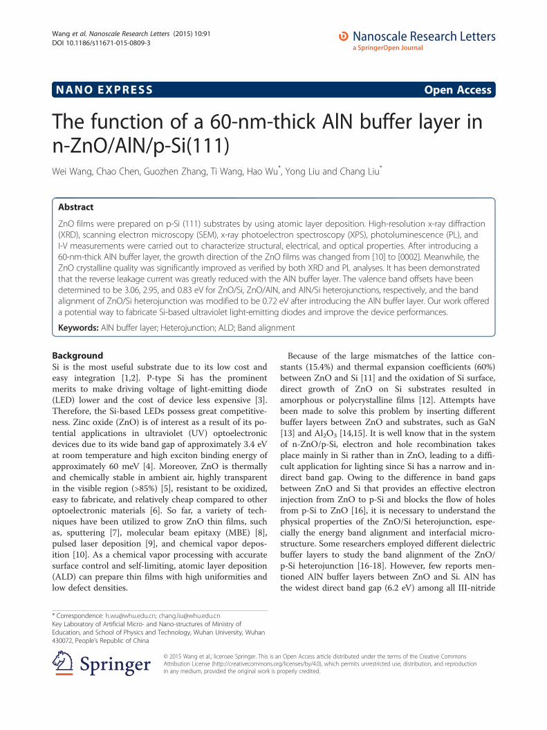
Figure 2 Cross-sectional SEM images of sample a and b.
The cross-sectional SEM images of samples A and Bare shown in Figure 2. The irregular cross profile ofsample A revealed a polycrystalline nature of the ZnOfilm grown without any buffer layer on Si. Figure 2bshows that the AlN buffer layer was introduced be-tween the ZnO film and Si substrate, and the thicknessof AlN buffer layer was measured to be 60 nm. It is ob-vious that the ZnO films in Figure 2b was regularly ori-ented while it was rambled in Figure 2a. The number ofstacking faults and edge dislocations of sample B wereobviously less than that of sample A. It can be con-cluded that with the AlN buffer layer, the crystallinequality of ZnO films was significantly improved.The room temperature PL spectra of ZnO thin films
with and without the AlN buffer layer are shown inFigure 3. The main PL peaks at about 380 nm were dueto the free excitation emission in ZnO, and a low en-ergy shoulder (at wavelength of 395 nm) was attribut-able to the emission related to point defects [24].Usually, the ratio of band-edge transition (BET) to deeplevel emissions (DLEs) could evaluate the quality ofZnO films. It has been shown that the quality of ZnOfilms has been significantly improved after inserting theAlN buffer layer, because the ratio of BET to DLE ofsample B (59.8) was larger than that of sample A (43.4).The DLE around 500 nm was caused by different in-trinsic defects in ZnO films such as oxygen vacanciesand zinc interstitials [14]. The very weak DLEs of sam-ples A and B suggest that few zinc interstitials and fewoxygen vacancies exist in the ZnO films, which can beattributed to the growth mechanism of ALD. Theself-limiting aspect of ALD leads to a conformal depos-ition, because the precursors can adsorb and subse-quently desorb from the surface where the reaction hasreached completion, and then proceed to react with
Figure 3 The room temperature PL spectra of samples a(without AlN) and b (with AlN). The inset shows the logarithmicintensity spectra.
Wang et al. Nanoscale Research Letters (2015) 10:91 Page 4 of 7
other unreacted surface areas, while the redundantformer precursor should be cleaned by the purge process.In this way, the two reactions (ZnOH* and Zn(CH2CH3)in this work) proceeded in a sequential fashion to deposita thin film with atomic level control [25].This can be further understood through the growth
procedures of ALD as shown in the following reac-tions [21]:
ZnOH� þ Zn CH2CH3ð Þ2→ZnOZn CH2CH3ð Þ� þ C2H6
Zn CH2CH3ð Þ� þ H2O→ZnOH� þ C2H6
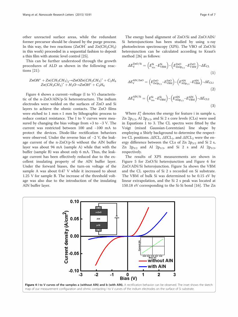
Figure 4 shows a current–voltage (I to V) characteris-tic of the n-ZnO/AlN/p-Si heterostructure. The indiumelectrodes were welded on the surfaces of ZnO and Silayers to achieve the ohmic contacts. The ZnO filmswere etched to 1 mm × 1 mm by lithographic process toreduce contact resistance. The I to V curves were mea-sured by changing the bias voltage from +3 to −3 V. Thecurrent was restricted between 100 and −100 mA toprotect the devices. Diode-like rectification behaviorswere observed. Under the reverse bias of −2 V, the leak-age current of the n-ZnO/p-Si without the AlN bufferlayer was about 94 mA (sample A) while that with thebuffer (sample B) was about only 6 mA. Thus, the leak-age current has been effectively reduced due to the ex-cellent insulating property of the AlN buffer layer.Under the forward biases, the turn-on voltage of thesample A was about 0.47 V while it increased to about1.25 V for sample B. The increase of the threshold volt-age was also due to the introduction of the insulatingAlN buffer layer.
Figure 4 I to V curves of the samples a (without AlN) and b (with AlNmap of our measurement configuration and ohmic contacting I to V curve
The energy band alignment of ZnO/Si and ZnO/AlN/Si heterojunctions has been studied by using x-rayphotoelectron spectroscopy (XPS). The VBO of ZnO/Siheterojunction can be calculated according to Kraut’smethod [26] as follows:
ΔEZnO=SiV ¼ ESi
Si2s−ESi
VBM
� �− EZnO
Zn2p3=2−EZnO
VBM
� �−ΔECL
ð1Þ
ΔEAlN=ZnOV ¼ EZnO
Zn2p3=2−EZnO
VBM
� �− EAlN
Al2p3=2−EAlN
VBM
� �−ΔECL1
ð2Þ
ΔEAlN=SiV ¼ ESi
Si2s−ESi
VBM
� �− EAlN
Al2p3=2−EAlN
VBM
� �−ΔECL2
ð3ÞWhere Es
i denotes the energy for feature i in sample s,Zn 2p3/2, Al 2p3/2, and Si 2 s core levels (CLs) were usedin Equations 1 to 3. The CL spectra were fitted by theVoigt (mixed Gaussian-Lorentzian) line shape byemploying a Shirly background to determine the respect-ive CL positions. ΔECL, ΔECL1, and ΔECL2 were the en-ergy difference between the CLs of Zn 2p3/2 and Si 2 s,Zn 2p3/2 and Al 2p3/2, and Si 2 s and Al 2p3/2,respectively.The results of XPS measurements are shown in
Figure 5 for ZnO/Si heterojunction and Figure 6 forZnO/AlN/Si heterojunction. Figure 5a shows the VBMand the CL spectra of Si 2 s recorded on Si substrate.The VBM of bulk Si was determined to be 0.15 eV bylinear extrapolation, and the Si 2 s peak was located at150.18 eV corresponding to the Si-Si bond [16]. The Zn
). A rectification behavior can be observed. The inset shows the sketchs of the indium electrodes on the surface of Si substrate.
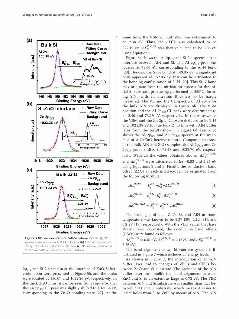
Figure 5 XPS narrow scans of ZnO/Si heterojunction. (a) XPSnarrow scans of Si 2 s and VBM of bulk Si; (b) XPS narrow scans ofZn 2p3/2 and Si 2 s at ZnO/Si interface; (c) XPS narrow scans of Zn2p3/2 and VBM of bulk ZnO on a Si substrate.
Wang et al. Nanoscale Research Letters (2015) 10:91 Page 5 of 7
2p3/2 and Si 2 s spectra at the interface of ZnO/Si het-erojunction were presented in Figure 5b, and the peakswere located at 150.07 and 1022.26 eV, respectively. Inthe thick ZnO films, it can be seen from Figure 5c thatthe Zn 2p3/2 CL peak was slightly shifted to 1021.54 eV,corresponding to the Zn-O bonding state [27]. At the
same time, the VBM of bulk ZnO was determined tobe 2.38 eV. Thus, the ΔECL was calculated to be
872.19 eV. ΔEZnO=SiV was then calculated to be 3.06 eV
using Equation 1.Figure 6a shows the Al 2p3/2 and Si 2 s spectra at the
interface between AlN and Si. The Al 2p3/2 peak waslocated at 73.66 eV, corresponding to the Al-N bond[28]. Besides, the Si-Si bond at 149.95 eV, a significantpeak appeared at 152.05 eV that can be attributed tothe bonding configuration of Si-N [29]. This Si-N bondmay originate from the nitridation process for the ini-tial Si substrate processing performed at 850°C, form-ing SiNx with an ultrathin thickness to be hardlymeasured. The VB and the CL spectra of Al 2p3/2 forthe bulk AlN are displayed in Figure 6b. The VBMposition and the Al 2p3/2 CL peak were determined tobe 2.40 and 73.19 eV, respectively. In the meanwhile,the VBM and the Zn 2p3/2 CL were deduced to be 2.14and 1021.38 eV for the bulk ZnO film with AlN bufferlayer from the results shown in Figure 6d. Figure 6cshows the Al 2p3/2 and Zn 2p3/2 spectra at the inter-face of AlN/ZnO heterostructure. Compared to thoseof the bulk AlN and ZnO samples, the Al 2p3/2 and Zn2p3/2 peaks shifted to 73.48 and 1022.76 eV, respect-
ively. With all the values obtained above, ΔEAlN=ZnOV
and ΔEAlN=SiV were calculated to be −0.83 and 2.95 eV
using Equations 2 and 3. Finally, the conduction bandoffset (ΔEC) at each interface can be estimated fromthe following formula:
ΔEZnO=SiC ¼ EZnO
g−ESi
g −ΔEZnO=SiV ð4Þ
ΔEAlN=SiC ¼ EAlN
g−ESi
g −ΔEAlN=SiV ð5Þ
ΔEAlN=ZnOC ¼ EAlN
g−EZnO
g −ΔEAlN=SiV ð6Þ
The band gap of bulk ZnO, Si, and AlN at roomtemperature was known to be 3.37 [30], 1.12 [31], and6.2 eV [19], respectively. With the VBO values that havealready been calculated, the conduction band offsets(CBOs) were found as follows:
ΔEZnO=SiC ¼ 0:81 eV, ΔEAlN=Si
C ¼ 2:13 eV, and ΔEAlN=ZnOC ¼
3:66 eV.The band alignment of two bi-interface systems is il-
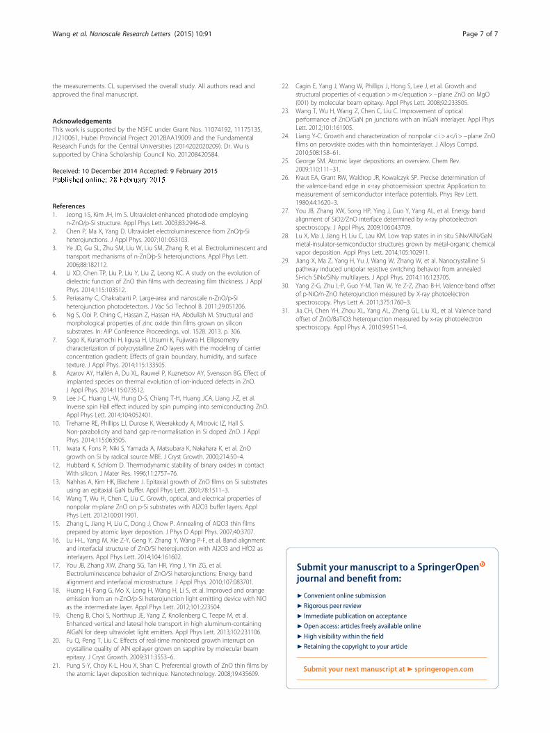
lustrated in Figure 7 which includes all energy levels.As shown in Figure 7, the introduction of an AlN
buffer layer lead to changes of VBOs and CBOs be-tween ZnO and Si substrate. The presence of the AlNbuffer layer can modify the band alignment betweenZnO and Si to an extent as large as 0.72 eV. The VBObetween AlN and Si substrate was smaller than that be-tween ZnO and Si substrate, which makes it easier toinject holes from Si to ZnO by means of AlN. The AlN
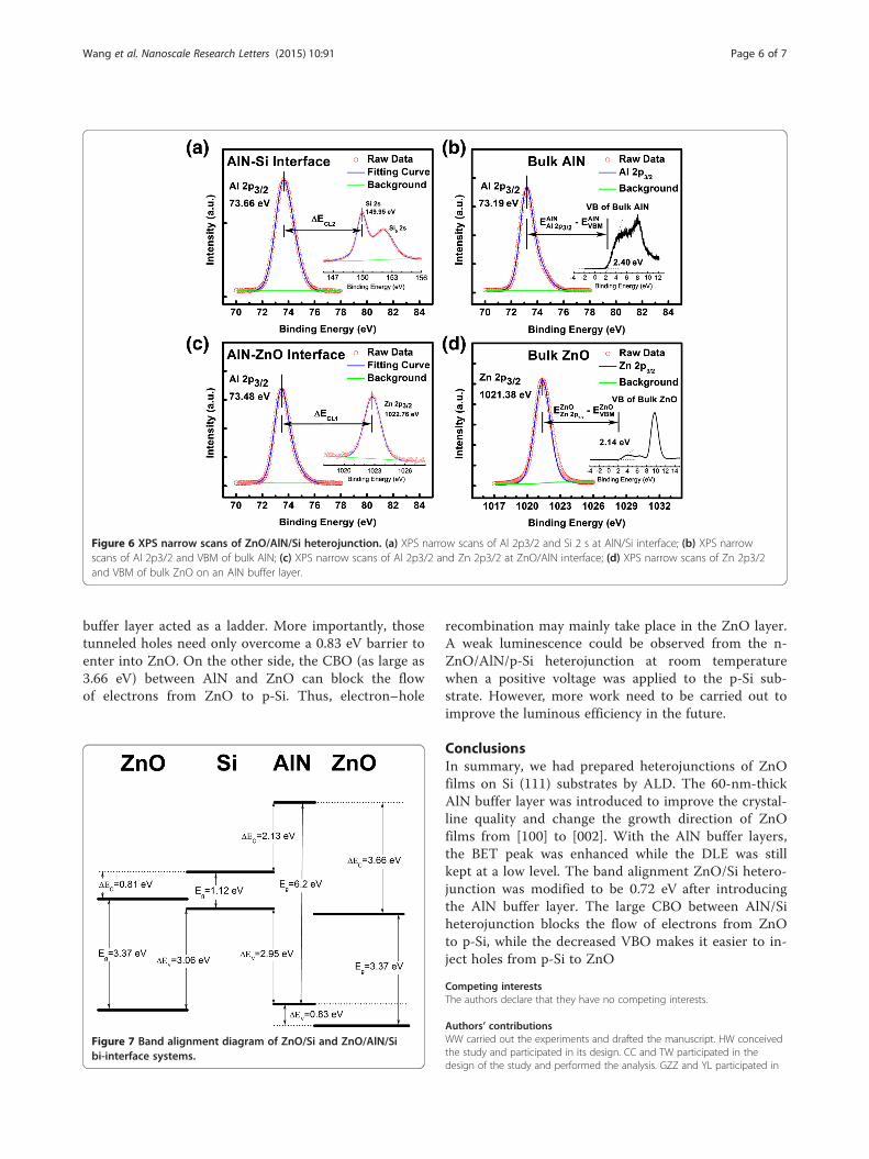
Figure 6 XPS narrow scans of ZnO/AlN/Si heterojunction. (a) XPS narrow scans of Al 2p3/2 and Si 2 s at AlN/Si interface; (b) XPS narrowscans of Al 2p3/2 and VBM of bulk AlN; (c) XPS narrow scans of Al 2p3/2 and Zn 2p3/2 at ZnO/AlN interface; (d) XPS narrow scans of Zn 2p3/2and VBM of bulk ZnO on an AlN buffer layer.
Wang et al. Nanoscale Research Letters (2015) 10:91 Page 6 of 7
buffer layer acted as a ladder. More importantly, thosetunneled holes need only overcome a 0.83 eV barrier toenter into ZnO. On the other side, the CBO (as large as3.66 eV) between AlN and ZnO can block the flowof electrons from ZnO to p-Si. Thus, electron–hole
Figure 7 Band alignment diagram of ZnO/Si and ZnO/AlN/Sibi-interface systems.
recombination may mainly take place in the ZnO layer.A weak luminescence could be observed from the n-ZnO/AlN/p-Si heterojunction at room temperaturewhen a positive voltage was applied to the p-Si sub-strate. However, more work need to be carried out toimprove the luminous efficiency in the future.
ConclusionsIn summary, we had prepared heterojunctions of ZnOfilms on Si (111) substrates by ALD. The 60-nm-thickAlN buffer layer was introduced to improve the crystal-line quality and change the growth direction of ZnOfilms from [100] to [002]. With the AlN buffer layers,the BET peak was enhanced while the DLE was stillkept at a low level. The band alignment ZnO/Si hetero-junction was modified to be 0.72 eV after introducingthe AlN buffer layer. The large CBO between AlN/Siheterojunction blocks the flow of electrons from ZnOto p-Si, while the decreased VBO makes it easier to in-ject holes from p-Si to ZnO
Competing interestsThe authors declare that they have no competing interests.
Authors’ contributionsWW carried out the experiments and drafted the manuscript. HW conceivedthe study and participated in its design. CC and TW participated in thedesign of the study and performed the analysis. GZZ and YL participated in
Wang et al. Nanoscale Research Letters (2015) 10:91 Page 7 of 7
the measurements. CL supervised the overall study. All authors read andapproved the final manuscript.
AcknowledgementsThis work is supported by the NSFC under Grant Nos. 11074192, 11175135,J1210061, Hubei Provincial Project 2012BAA19009 and the FundamentalResearch Funds for the Central Universities (2014202020209). Dr. Wu issupported by China Scholarship Council No. 201208420584.
Received: 10 December 2014 Accepted: 9 February 2015
References1. Jeong I-S, Kim JH, Im S. Ultraviolet-enhanced photodiode employing
n-ZnO/p-Si structure. Appl Phys Lett. 2003;83:2946–8.2. Chen P, Ma X, Yang D. Ultraviolet electroluminescence from ZnO∕p‐Si
heterojunctions. J Appl Phys. 2007;101:053103.3. Ye JD, Gu SL, Zhu SM, Liu W, Liu SM, Zhang R, et al. Electroluminescent and
transport mechanisms of n-ZnO∕p-Si heterojunctions. Appl Phys Lett.2006;88:182112.
4. Li XD, Chen TP, Liu P, Liu Y, Liu Z, Leong KC. A study on the evolution ofdielectric function of ZnO thin films with decreasing film thickness. J ApplPhys. 2014;115:103512.
5. Periasamy C, Chakrabarti P. Large-area and nanoscale n-ZnO/p-Siheterojunction photodetectors. J Vac Sci Technol B. 2011;29:051206.
6. Ng S, Ooi P, Ching C, Hassan Z, Hassan HA, Abdullah M. Structural andmorphological properties of zinc oxide thin films grown on siliconsubstrates. In: AIP Conference Proceedings, vol. 1528. 2013. p. 306.
7. Sago K, Kuramochi H, Iigusa H, Utsumi K, Fujiwara H. Ellipsometrycharacterization of polycrystalline ZnO layers with the modeling of carrierconcentration gradient: Effects of grain boundary, humidity, and surfacetexture. J Appl Phys. 2014;115:133505.
8. Azarov AY, Hallén A, Du XL, Rauwel P, Kuznetsov AY, Svensson BG. Effect ofimplanted species on thermal evolution of ion-induced defects in ZnO.J Appl Phys. 2014;115:073512.
9. Lee J-C, Huang L-W, Hung D-S, Chiang T-H, Huang JCA, Liang J-Z, et al.Inverse spin Hall effect induced by spin pumping into semiconducting ZnO.Appl Phys Lett. 2014;104:052401.
10. Treharne RE, Phillips LJ, Durose K, Weerakkody A, Mitrovic IZ, Hall S.Non-parabolicity and band gap re-normalisation in Si doped ZnO. J ApplPhys. 2014;115:063505.
11. Iwata K, Fons P, Niki S, Yamada A, Matsubara K, Nakahara K, et al. ZnOgrowth on Si by radical source MBE. J Cryst Growth. 2000;214:50–4.
12. Hubbard K, Schlom D. Thermodynamic stability of binary oxides in contactWith silicon. J Mater Res. 1996;11:2757–76.
13. Nahhas A, Kim HK, Blachere J. Epitaxial growth of ZnO films on Si substratesusing an epitaxial GaN buffer. Appl Phys Lett. 2001;78:1511–3.
14. Wang T, Wu H, Chen C, Liu C. Growth, optical, and electrical properties ofnonpolar m-plane ZnO on p-Si substrates with Al2O3 buffer layers. ApplPhys Lett. 2012;100:011901.
15. Zhang L, Jiang H, Liu C, Dong J, Chow P. Annealing of Al2O3 thin filmsprepared by atomic layer deposition. J Phys D Appl Phys. 2007;40:3707.
16. Lu H-L, Yang M, Xie Z-Y, Geng Y, Zhang Y, Wang P-F, et al. Band alignmentand interfacial structure of ZnO/Si heterojunction with Al2O3 and HfO2 asinterlayers. Appl Phys Lett. 2014;104:161602.
17. You JB, Zhang XW, Zhang SG, Tan HR, Ying J, Yin ZG, et al.Electroluminescence behavior of ZnO/Si heterojunctions: Energy bandalignment and interfacial microstructure. J Appl Phys. 2010;107:083701.
18. Huang H, Fang G, Mo X, Long H, Wang H, Li S, et al. Improved and orangeemission from an n-ZnO/p-Si heterojunction light emitting device with NiOas the intermediate layer. Appl Phys Lett. 2012;101:223504.
19. Cheng B, Choi S, Northrup JE, Yang Z, Knollenberg C, Teepe M, et al.Enhanced vertical and lateral hole transport in high aluminum-containingAlGaN for deep ultraviolet light emitters. Appl Phys Lett. 2013;102:231106.
20. Fu Q, Peng T, Liu C. Effects of real-time monitored growth interrupt oncrystalline quality of AlN epilayer grown on sapphire by molecular beamepitaxy. J Cryst Growth. 2009;311:3553–6.
21. Pung S-Y, Choy K-L, Hou X, Shan C. Preferential growth of ZnO thin films bythe atomic layer deposition technique. Nanotechnology. 2008;19:435609.
22. Cagin E, Yang J, Wang W, Phillips J, Hong S, Lee J, et al. Growth andstructural properties of < equation >m</equation > −plane ZnO on MgO(001) by molecular beam epitaxy. Appl Phys Lett. 2008;92:233505.
23. Wang T, Wu H, Wang Z, Chen C, Liu C. Improvement of opticalperformance of ZnO/GaN pn junctions with an InGaN interlayer. Appl PhysLett. 2012;101:161905.
24. Liang Y-C. Growth and characterization of nonpolar < i > a</i > −plane ZnOfilms on perovskite oxides with thin homointerlayer. J Alloys Compd.2010;508:158–61.
25. George SM. Atomic layer depositions: an overview. Chem Rev.2009;110:111–31.
26. Kraut EA, Grant RW, Waldrop JR, Kowalczyk SP. Precise determination ofthe valence-band edge in x-ray photoemission spectra: Application tomeasurement of semiconductor interface potentials. Phys Rev Lett.1980;44:1620–3.
27. You JB, Zhang XW, Song HP, Ying J, Guo Y, Yang AL, et al. Energy bandalignment of SiO2/ZnO interface determined by x-ray photoelectronspectroscopy. J Appl Phys. 2009;106:043709.
28. Lu X, Ma J, Jiang H, Liu C, Lau KM. Low trap states in in situ SiNx/AlN/GaNmetal-insulator-semiconductor structures grown by metal-organic chemicalvapor deposition. Appl Phys Lett. 2014;105:102911.
29. Jiang X, Ma Z, Yang H, Yu J, Wang W, Zhang W, et al. Nanocrystalline Sipathway induced unipolar resistive switching behavior from annealedSi-rich SiNx/SiNy multilayers. J Appl Phys. 2014;116:123705.
30. Yang Z-G, Zhu L-P, Guo Y-M, Tian W, Ye Z-Z, Zhao B-H. Valence-band offsetof p-NiO/n-ZnO heterojunction measured by X-ray photoelectronspectroscopy. Phys Lett A. 2011;375:1760–3.
31. Jia CH, Chen YH, Zhou XL, Yang AL, Zheng GL, Liu XL, et al. Valence bandoffset of ZnO/BaTiO3 heterojunction measured by x-ray photoelectronspectroscopy. Appl Phys A. 2010;99:511–4.
Submit your manuscript to a journal and benefi t from:
7 Convenient online submission
7 Rigorous peer review
7 Immediate publication on acceptance
7 Open access: articles freely available online
7 High visibility within the fi eld
7 Retaining the copyright to your article
Submit your next manuscript at 7 springeropen.com
Related Documents