The Fabrication and Characterisation of Piezoelectric Actuators for Active X-ray Optics Dou Zhang a* , Daniel Rodriguez Sanmartin a , Tim W Button a , Carl Meggs a , Carolyn Atkins b , ter Doel b , David Brooks b , Charlotte Feldman c , Richard Willingale c , Alan Michette d , Slawk Pfauntsch d , Shahin Sahraei d , Ady James e , Camelia Dunare f , Tom Stevenson f , William Parkes f , Andrew Smith g , Hongchang Wang h Pe a a School of Metallurgy and Materials, University of Birmingham, Edgbaston, Birmingham, B15 2TT, UK b Department of Physics and Astronomy, University College London, Gower Street, London, WC1E 6BT, UK c Department of Physics and Astronomy, University of Leicester, Leicester, LE1 7RH, UK d Department of Physics, King’s College London, Strand, London WC2R 2LS, UK e Mullard Space Science Laboratory, University College London, Holmbury St. Mary, Dorking, Surrey, RH5 6NT, UK f Scottish Microelectronics Centre, School of Engineering and Electronics, University of Edinburgh, West Mains Road, Edinburgh, EH9 3JF, UK g STFC - Daresbury Laboratory, Keckwick Lane, Warrington, Cheshire, WA4 4AD, UK h Diamond Light Source Ltd, Harwell Science and Innovation Campus, Didcot, Oxfordshire, OX11 0DE, UK ABSTRACT Piezoelectric actuators are widely employed in adaptive optics to enable an actively controlled mirror surface and improve the optical resolution and sensitivity. Currently two new prototype adaptive X-ray optical systems are under development through the Smart X-ray Optics project in a UK based consortium. One proposed technology is micro- structured optical arrays (MOAs) which uses aligned micro-channels structures obtained by deep silicon etching using both dry and wet techniques and bonded piezoelectric actuators to produce a micro-focused X-ray source for biological applications. The other technology is large scale optics which uses a thin shell mirror segment with 20-40 bonded piezo- actuators for the next generation of X-ray telescopes with an aim to achieve a resolution greater than that currently available by Chandra (0.5”). The Functional Materials Group of Birmingham University has the capability of fabricating a wide range of piezo- actuators including, for example, unimorph, bimorph and active fibre composites (AFC) by using a viscous plastic processing technique. This offers flexibility in customising the shapes (from planar to 3-D helix) and feature sizes (>20 μm) of the actuators, as well as achieving good piezoelectric properties. PZT unimorph actuators are being developed in this programme according to the design and implementation of the proposed mirror and array structures. Precise controls on the dimension, thickness, surface finishing and the curvature have been achieved for delivering satisfactory actuators. Results are presented regarding the fabrication and characterisation of such piezo-actuators, as well as the progress on the large optic and MOAs prototypes employing the piezo-actuators. Keywords: Piezoelectric actuators, PZT, active X-ray Optics, X-ray telescopes, micro-structured optical arrays * Further author information: email: [email protected] Advances in X-Ray/EUV Optics and Components IV, edited by Ali M. Khounsary, Christian Morawe, Shunji Goto, Proc. of SPIE Vol. 7448, 744807 · © 2009 SPIE · CCC code: 0277-786X/09/$18 · doi: 10.1117/12.826018 Proc. of SPIE Vol. 7448 744807-1

Welcome message from author
This document is posted to help you gain knowledge. Please leave a comment to let me know what you think about it! Share it to your friends and learn new things together.
Transcript
The Fabrication and Characterisation of Piezoelectric Actuators for
Active X-ray Optics
Dou Zhang a *, Daniel Rodriguez Sanmartin a, Tim W Button a, Carl Meggs a, Carolyn Atkins b,ter Doel b, David Brooks b, Charlotte Feldman c, Richard Willingale c, Alan Michette d, Slawk
Pfauntsch d, Shahin Sahraei d, Ady James e, Camelia Dunare f, Tom Stevenson f, William Parkes f,Andrew Smith g, Hongchang Wang h
Pe a
a School of Metallurgy and Materials, University of Birmingham, Edgbaston, Birmingham, B15 2TT, UK
b Department of Physics and Astronomy, University College London, Gower Street, London, WC1E 6BT, UK
c Department of Physics and Astronomy, University of Leicester, Leicester, LE1 7RH, UK d Department of Physics, King’s College London, Strand, London WC2R 2LS, UK
e Mullard Space Science Laboratory, University College London, Holmbury St. Mary, Dorking, Surrey, RH5 6NT, UK
f Scottish Microelectronics Centre, School of Engineering and Electronics, University of Edinburgh, West Mains Road, Edinburgh, EH9 3JF, UK
g STFC - Daresbury Laboratory, Keckwick Lane, Warrington, Cheshire, WA4 4AD, UK h Diamond Light Source Ltd, Harwell Science and Innovation Campus, Didcot, Oxfordshire,
OX11 0DE, UK
ABSTRACT Piezoelectric actuators are widely employed in adaptive optics to enable an actively controlled mirror surface and improve the optical resolution and sensitivity. Currently two new prototype adaptive X-ray optical systems are under development through the Smart X-ray Optics project in a UK based consortium. One proposed technology is micro-structured optical arrays (MOAs) which uses aligned micro-channels structures obtained by deep silicon etching using both dry and wet techniques and bonded piezoelectric actuators to produce a micro-focused X-ray source for biological applications. The other technology is large scale optics which uses a thin shell mirror segment with 20-40 bonded piezo-actuators for the next generation of X-ray telescopes with an aim to achieve a resolution greater than that currently available by Chandra (0.5”).
The Functional Materials Group of Birmingham University has the capability of fabricating a wide range of piezo-actuators including, for example, unimorph, bimorph and active fibre composites (AFC) by using a viscous plastic processing technique. This offers flexibility in customising the shapes (from planar to 3-D helix) and feature sizes (>20 μm) of the actuators, as well as achieving good piezoelectric properties. PZT unimorph actuators are being developed in this programme according to the design and implementation of the proposed mirror and array structures. Precise controls on the dimension, thickness, surface finishing and the curvature have been achieved for delivering satisfactory actuators. Results are presented regarding the fabrication and characterisation of such piezo-actuators, as well as the progress on the large optic and MOAs prototypes employing the piezo-actuators.
Keywords: Piezoelectric actuators, PZT, active X-ray Optics, X-ray telescopes, micro-structured optical arrays
* Further author information: email: [email protected]
Advances in X-Ray/EUV Optics and Components IV, edited by Ali M. Khounsary, Christian Morawe, Shunji Goto,Proc. of SPIE Vol. 7448, 744807 · © 2009 SPIE · CCC code: 0277-786X/09/$18 · doi: 10.1117/12.826018
Proc. of SPIE Vol. 7448 744807-1
1. INTRODUCTIONTwo new prototype adaptive X-ray optic systems are under development in a UK consortium “Smart X-ray Optics” (SXO) with the aim of approaching the fundamental diffraction limit. One proposed technology is microstructured optical arrays (MOAs) 1 involving two or four piezoelectric strips bonded to a 10 mm×20 mm silicon wafer to produce a micro-focused X-ray source for biological applications, and which uses grazing incidence reflection through consecutive aligned arrays of channels obtained using deep silicon etching.2 The other interest is actively deformable mirrors in large scale optics for the next generation of X-ray telescopes with an aim to achieve a spatial resolution greater than that currently available by Chandra (0.5”) whilst having a high throughput.3 Thin nickel shells fabricated by an electroforming method are employed in this application.4 An X-ray reflective coating is applied on one side of the nickel shell, while a series of piezoelectric actuators are bonded on the other side to provide the active control.5 Detailed reports on the first prototype large optic system are presented elsewhere at this conference by Feldman et al. 6 and Atkins et al. 7.
Lead zirconate titanate (PZT) membranes with controlled surface finish, thickness and curvature have been developed for the SXO project using a viscous plastic process (VPP) technique.8 VPP process generally provides improved material properties compared to conventional dry powder pressing and slip casting due to its capability of breaking down the agglomerates even in high solids loading paste systems. Good plasticity in the green state facilitates complex shaping processes and the control of membrane thickness, i.e. 50-200 μm in this study, with density and piezoelectric properties similar to the bulk values, offers the flexibility of curving the membrane to the required radius of curvature.
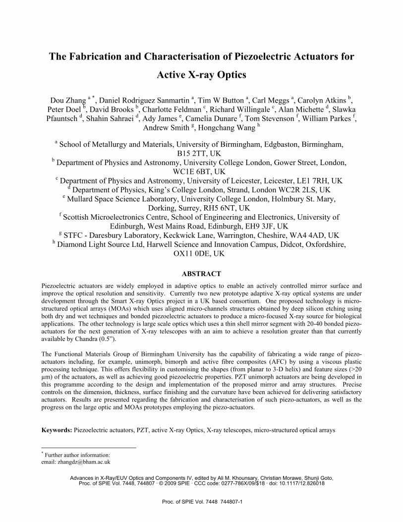
2. GENERAL VISCOUS PLASTIC PROCESS Viscous plastic processing (VPP) has been utilised for the fabrication of a wide range of net shape ceramic structures, as shown in Figure 1. 9 Ceramic powders were incorporated with either aqueous or non-aqueous polymer binder systems, and suitable additives using a high shear twin-roll milling technique. Aqueous binder systems are normally based on polyvinyl alcohol (PVA) and water whereas the non-aqueous systems comprise polyvinyl butyral (PVB) and cyclohexanone, the choice depending on the actual processing and forming routes being used. The ceramic dough or paste obtained after twin-roll milling has a shear viscosity of approximately 105 Pa s at a shear rate of 5-10 s-1. Net shape ceramic components and devices such as rods, tubes and domes can be fabricated via extrusion, calendering or pressing of the dough. This technique is capable of producing complex structures via a conventional plastic processing route. For example, 3-D bimorph structures can be obtained by using calendered tapes which are screen printed with platinum thick film ink to form the internal and external electrodes, laminated, cut to the required length and width, and then wound into the required shape.
Twin-Roll Milling
Ceramic Paste or Dough
ExtrusionCalenderingLaminating
Pressing
Press Forming
Pressing/Lost mould
Rods/fibresTubesSheetsSpringsDomes Bimorphs New Devices
Ceramic Powder
(e.g. PZT-5A or PZT-4D)
Polymer Binder (PVA
or PVB) /Solvent
Thick Films
Fine-scale Structures Processing
Additives
Figure 1 A general flow chart for the fabrication of net shape piezoelectric devices and structures using viscous plastic processing
Proc. of SPIE Vol. 7448 744807-2
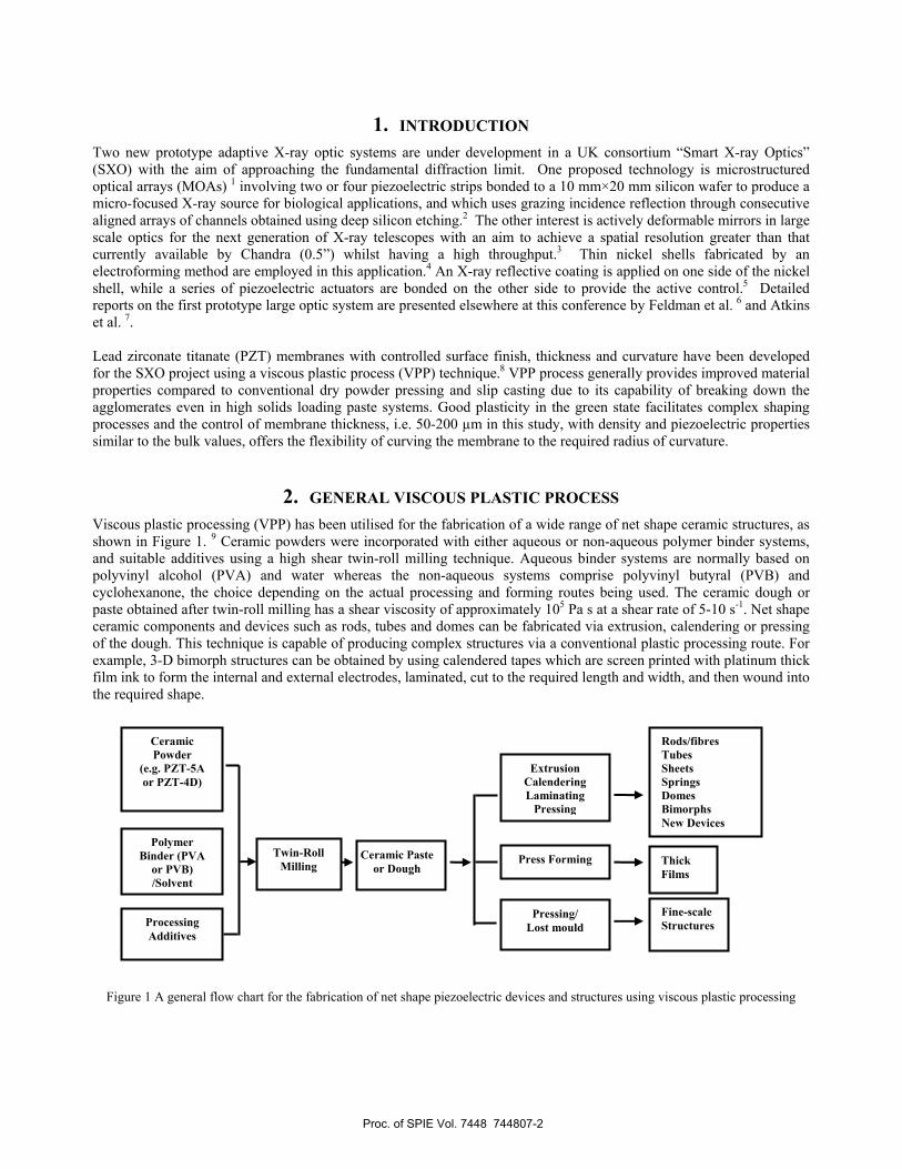
Figure 2 shows a range of net shape piezoelectric bimorph device structures based on the concept of incorporating bimorph tapes into various spiral and helical structures.10 A PZT bimorph spiral is shown in Figure 2(a). The device comprised two PZT layers each of thickness 0.27 mm, wound into a spiral of overall diameter 9.8 mm. A wide range of helical bimorph structures have been produced with primary diameters ranging from 2.5 to 20mm, and various tape widths and pitches, as shown in Figure 2(b). Helical bimorphs with a primary diameter which have been wound into a secondary helix are termed super helices or ‘Helimorphs’†, as shown in Figure 2(c), resulting in an actuation mode such that linear actuation is achieved along the axis of the secondary helix. These devices have potential application as transducers and actuators in active control systems.
d
RI
(b)(a)
(c)
Figure 2 Three typical types of net shape PZT bimorph device structures. (a) spiral bimorph. d = 0.540 mm, R1 = 1.337 mm. (b) PZT bimorph helices. (c) PZT Helimorphs.
† Helimorph® is the trademark of 1 Limited, Cambridge, UK.
Proc. of SPIE Vol. 7448 744807-3
3. PRODUCTION METHODS In this study TRS610C PZT powders (TRS Technologies, Inc., USA) were mixed with polyvinyl butyral (PVB), solvent and plasticisers and twin-roll milled to obtain the dough. The VPP ceramic dough was shaped into membranes with controlled thickness using a calendering and laminating process. Typical thickness of the green tape ranged from 50 μm to 200 μm. The green membranes were then subjected to drying, binder removal, and sintering processes. The sintering was carried out at 1200°C on zirconia formers in a controlled PbO-rich atmosphere for 1 hr. The electrodes were applied by sputtering Cr and Au for 2 min and 4 min, respectively.
3.1. Precision control Accurate prediction of the shrinkages during various stages of the ceramic process is generally desired necessitating excellent homogeneity and good repeatability from batch to batch. Table 1 shows typical data of linear shrinkages for a PZT tape material in stages of drying and sintering, respectively. The main discrepancy exists in the stage of drying while 50-100% more shrinkage happens in the shearing direction (i.e. direction of calendering) than in other directions.
Table 1. Typical linear shrinkages associated with drying and sintering for a typical PZT calendered tape.
Direction relative to shearing
Linear shrinkage wet – dry
(%)
Linear shrinkage green – sintered
(%)-45° 4.4 14.2
0° 6.4 14.3
45° 4.0 14.1
90° 3.0 14.1
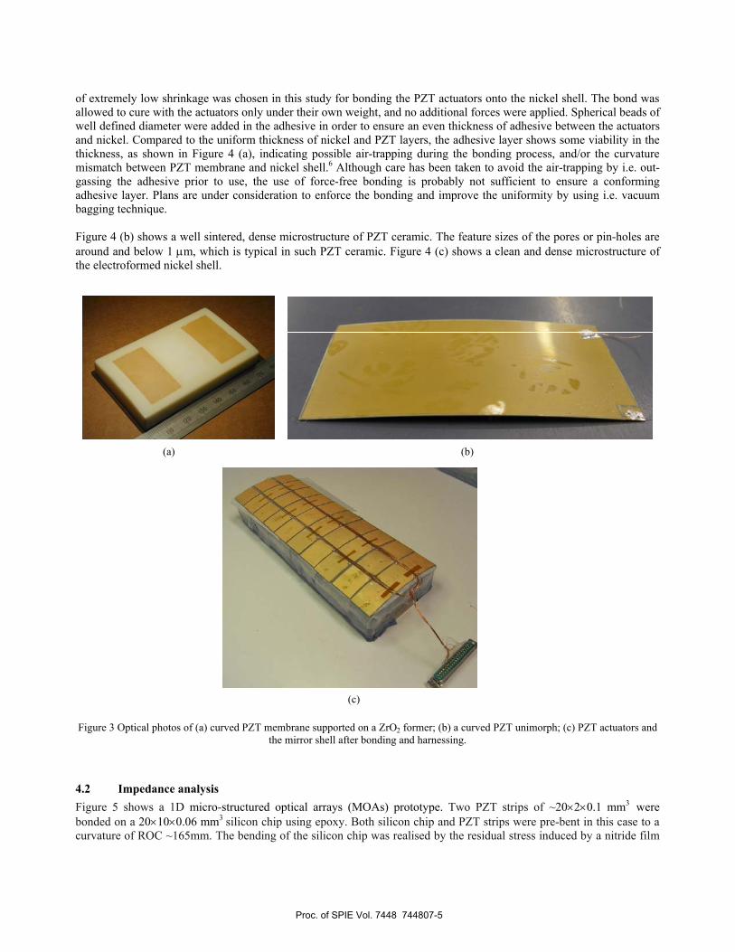
3.2. Curving and harnessing PZT actuators In order to match the curvature of the mirror shell in the large optic applications and reduce the bonding stress and possible mirror distortion, a curving technique was developed to shape PZT membranes into an appropriate curvature. Figure 3 (a) shows a ZrO2 former whose top surface has the required curvature, with two pieces of PZT membranes resting on top after the sintering process. The curvature of the PZT membrane was obtained via a softening effect during the heat treatment process. The ZrO2 formers can withstand much higher temperature than those required for sintering the PZT. Two routes have been utilised here for curving the membrane. One is the direct curving process by using the green PZT tape. Both sintering and curving can be obtained from a single cycle of sintering. The other route is to sinter the membrane in a conventional process. After obtaining the sintered membrane in a flat form, a further precision control on the thickness and the surface finish can be performed by a precision lapping machine (Logitech PM5, Glasgow, UK). Finally the membranes can be reshaped to a controlled curvature by heating on the former. Route 1 is more cost-effective but lacks of the control on the thickness and surface finishing, and therefore requires accurate knowledge of the drying and sintering shrinkages to enable a satisfactory delivery of the final products. Figure 3 (b) shows a close-up photograph of a PZT unimorph, with Cr/Au electrodes and two leads to access both electrode areas.
In the first ellipsoidal prototype, 30 pieces of curved PZT unimorph were bonded to a nickel optic shell. 60 wires were harnessed using vacuum compatible acrylic adhesive tape. Figure 3 (c) shows such a completed large scale optic prototype.
4. PIEZOELECTRIC ACTUATORS
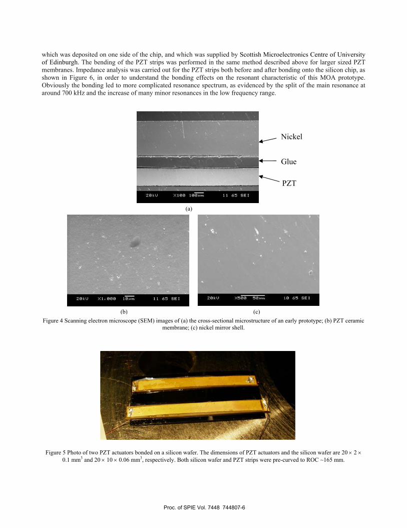
4.1 Microstructural analysis A cross section of PZT actuator/bond/Ni shell structure was examined by using scanning electron microscopy, as shown in Figure 4, revealing Ni, PZT and adhesive layers of 0.4 mm, 0.2 mm and 0.1 mm thickness, respectively. An adhesive
Proc. of SPIE Vol. 7448 744807-4
of extremely low shrinkage was chosen in this study for bonding the PZT actuators onto the nickel shell. The bond was allowed to cure with the actuators only under their own weight, and no additional forces were applied. Spherical beads of well defined diameter were added in the adhesive in order to ensure an even thickness of adhesive between the actuators and nickel. Compared to the uniform thickness of nickel and PZT layers, the adhesive layer shows some viability in the thickness, as shown in Figure 4 (a), indicating possible air-trapping during the bonding process, and/or the curvature mismatch between PZT membrane and nickel shell.6 Although care has been taken to avoid the air-trapping by i.e. out-gassing the adhesive prior to use, the use of force-free bonding is probably not sufficient to ensure a conforming adhesive layer. Plans are under consideration to enforce the bonding and improve the uniformity by using i.e. vacuum bagging technique.
Figure 4 (b) shows a well sintered, dense microstructure of PZT ceramic. The feature sizes of the pores or pin-holes are around and below 1 m, which is typical in such PZT ceramic. Figure 4 (c) shows a clean and dense microstructure of the electroformed nickel shell.
(a) (b)
(c)
Figure 3 Optical photos of (a) curved PZT membrane supported on a ZrO2 former; (b) a curved PZT unimorph; (c) PZT actuators and the mirror shell after bonding and harnessing.
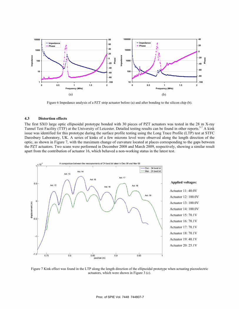
4.2 Impedance analysis Figure 5 shows a 1D micro-structured optical arrays (MOAs) prototype. Two PZT strips of ~20 2 0.1 mm3 were bonded on a 20 10 0.06 mm3 silicon chip using epoxy. Both silicon chip and PZT strips were pre-bent in this case to a curvature of ROC ~165mm. The bending of the silicon chip was realised by the residual stress induced by a nitride film
Proc. of SPIE Vol. 7448 744807-5
(nu :iiti.
20kV )(500 øw.n 10 65 SE!
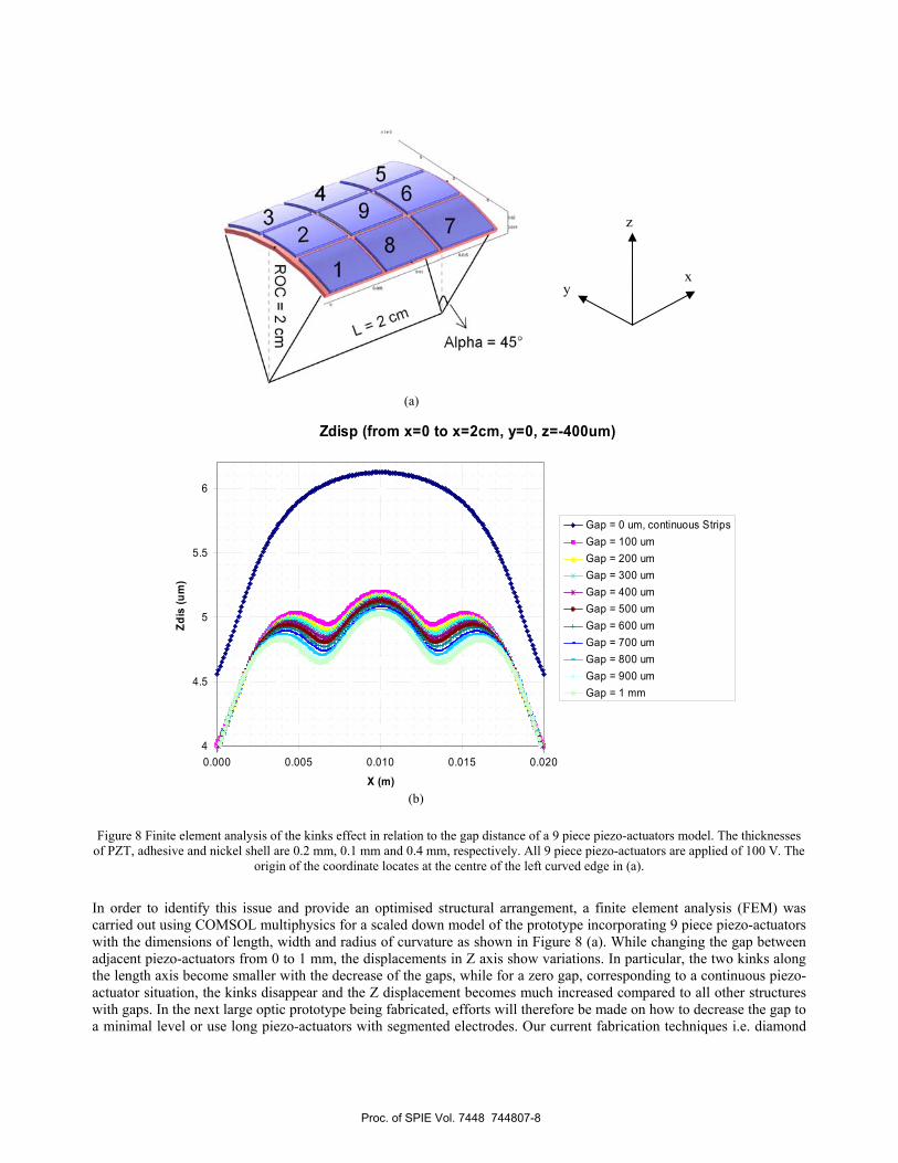
which was deposited on one side of the chip, and which was supplied by Scottish Microelectronics Centre of University of Edinburgh. The bending of the PZT strips was performed in the same method described above for larger sized PZT membranes. Impedance analysis was carried out for the PZT strips both before and after bonding onto the silicon chip, as shown in Figure 6, in order to understand the bonding effects on the resonant characteristic of this MOA prototype. Obviously the bonding led to more complicated resonance spectrum, as evidenced by the split of the main resonance at around 700 kHz and the increase of many minor resonances in the low frequency range.
Figure 4 Scanning electron microscope (SEM) images of (a) the cross-sectional microstructure of an early prototype; (b) PZT ceramic membrane; (c) nickel mirror shell.
Glue
Nickel
(a)
(b) (c)
PZT
Figure 5 Photo of two PZT actuators bonded on a silicon wafer. The dimensions of PZT actuators and the silicon wafer are 20 2 0.1 mm3 and 20 10 0.06 mm3, respectively. Both silicon wafer and PZT strips were pre-curved to ROC ~165 mm.
Proc. of SPIE Vol. 7448 744807-6
1
10
100
1000
10000
0 0.5 1 1.5 2Frequency (MHz)
Impe
danc
e
-100
-80
-60
-40
-20
0
20
40
60
80
Phas
e
10
100
1000
10000
100000
0 0.5 1 1.5 2Frequency (MHz)
Impe
danc
e
-100
-80
-60
-40
-20
0
20
40
Phas
e
ImpedanceImpedancePhasePhase
(a) (b)
Figure 6 Impedance analysis of a PZT strip actuator before (a) and after bonding to the silicon chip (b).
4.3 Distortion effects The first SXO large optic ellipsoidal prototype bonded with 30 pieces of PZT actuators was tested in the 28 m X-ray Tunnel Test Facility (TTF) at the University of Leicester. Detailed testing results can be found in other reports.5-7 A kink issue was identified for this prototype during the surface profile testing using the Long Trace Profile (LTP) test at STFC Daresbury Laboratory, UK. A series of kinks of a few microns level were observed along the length direction of the optic, as shown in Figure 7, with the maximum change of curvature located at places corresponding to the gaps between the PZT actuators. Two scans were performed in December 2008 and March 2009, respectively, showing a similar result apart from the contribution of actuator 16, which behaved a non-working status in the latest test.
Applied voltages:
Actuator 11: 40.0V
Actuator 12: 100.0V
Actuator 13: 100.0V
Actuator 14: 100.0V
Actuator 15: 70.1V
Actuator 16: 70.1V
Actuator 17: 70.1V
Actuator 18: 70.1V
Actuator 19: 40.1V
Actuator 20: 25.1V
Figure 7 Kink effect was found in the LTP along the length direction of the ellipsoidal prototype when actuating piezoelectric actuators, which were shown in Figure 3 (c).
Proc. of SPIE Vol. 7448 744807-7
z
xy
(a)
Zdisp (from x=0 to x=2cm, y=0, z=-400um)
4
4.5
5
5.5
6
0.000 0.005 0.010 0.015 0.020
X (m)
Zdis
(um
)
Gap = 0 um, continuous StripsGap = 100 umGap = 200 umGap = 300 umGap = 400 umGap = 500 umGap = 600 umGap = 700 umGap = 800 umGap = 900 umGap = 1 mm
(b)
Figure 8 Finite element analysis of the kinks effect in relation to the gap distance of a 9 piece piezo-actuators model. The thicknesses of PZT, adhesive and nickel shell are 0.2 mm, 0.1 mm and 0.4 mm, respectively. All 9 piece piezo-actuators are applied of 100 V. The
origin of the coordinate locates at the centre of the left curved edge in (a).
In order to identify this issue and provide an optimised structural arrangement, a finite element analysis (FEM) was carried out using COMSOL multiphysics for a scaled down model of the prototype incorporating 9 piece piezo-actuators with the dimensions of length, width and radius of curvature as shown in Figure 8 (a). While changing the gap between adjacent piezo-actuators from 0 to 1 mm, the displacements in Z axis show variations. In particular, the two kinks along the length axis become smaller with the decrease of the gaps, while for a zero gap, corresponding to a continuous piezo-actuator situation, the kinks disappear and the Z displacement becomes much increased compared to all other structures with gaps. In the next large optic prototype being fabricated, efforts will therefore be made on how to decrease the gap to a minimal level or use long piezo-actuators with segmented electrodes. Our current fabrication techniques i.e. diamond
Proc. of SPIE Vol. 7448 744807-8
saw cutting and lapping after sintering, are difficult to deliver smooth and ideal parallel edges in order to realise the gap level down to a few hundreds micron. Laser micromachining is an ideal tool for trimming the edges in this application for high level precision control, and will be explored for piezo-actuators in the following-on prototypes.
5. SUMMARY AND FUTURE WORK Piezoelectric actuators have been chosen as the active controlling component in smart X-ray optic applications, including cylindrical and ellipsoidal shaped large optics and microstructured optical arrays. Customized piezoelectric membranes have been developed using a viscous plastic processing technique, which shows advantages in the fabrication of net shape components with complex shape. Precise controls of the thickness, surface finishing and the curvature of the PZT actuators have been realised according to the design and implementation of the proposed mirror and array structures. Both LTP test and FEM simulation indicated a distortion effect due to the existence of gaps between the piezo-actuators bonded on the back surface of nickel shell. In new prototypes, Laser micromachining will be employed in order to deliver actuators with parallel edges thus minimising the gap between adjacent piezo-actuators on the nickel shell. Techniques are under development for the fabrication of longer piezo-actuators, i.e. 70-100 mm, while maintaining the required curvature and integrity.
ACKNOWLEDGMENTS This work is supported by a Basic technologies Grant from the UK Engineering and Physical Sciences Research Council (EPSRC). The authors would like to thank the help and advice offered by fellow members of the SXO consortium.
REFERENCES [1] Michette, A., Button, T., Dunare, C., Feldman, C., Folkard, M., Hart, D., McFaul, C., Morrison, G. R., Parkes, W.,
Pfauntsch, S., Powell, A. K., Rodriguez-Sanmartin, D., Sahraei, S., Stevenson, T., Vojnovic, B., Willingaled, R., and Zhang, D., "Active micro-structured arrays for X-ray optics," Proc. of SPIE 6705, 670502 (2007).
[2] Dunare, C., Parkes, W., Stevenson, T., Michette, A., Pfauntsch, S., Sahraei, S., Shand, M., Zhang, D., Rodriguez Sanmartin, D., Button, T., Feldman, C., Willingale, R., Doel, P., Wang, H., and James, A., "Microstructured optical arrays for smart x-ray optics," Proc. of SPIE 7360, 736015 (2009).
[3] Doel, P., Atkins, C., Thompson, S., Brooks, D., Yao, J., Feldman, C., Willingale, R., Button, T., Zhang, D., and James, A., "Large thin adaptive X-ray mirrors," Proc. of SPIE 6705, 67050M (2007).
[4] Atkins, C., Wang, H., Doel, P., Brooks, D., Thompson, S., Feldman, C., Willingale, R., Button, T., Sanmartin, D. R., Zhang, D., James, A., and Theobald, C., "Future high-resolution x-ray telescope technologies: prototype fabrication methods and finite element analysis," Proc. of SPIE 7011, 70110X (2008).
[5] Atkins, C., Wang, H., Doel, P., Brooks, D., Thompson, S., Feldman, C., Willingale, R., Button, T., Rodriguez Sanmartin, D., Zhang, D., James, A., Theobald, C., Willis, G., and Smith, A., "Active x-ray optics for the next generation of x-ray telescopes," Proc. of SPIE 7360, 736008 (2009).
[6] Feldman, C., Willingale, R., Atkins, C., Wang, H., Doel, P., Brooks, D., Thompson, S., Button, T., Zhang, D., Rodriguez Sanmartin, D., James, A., and Theobald, C., "First results from the testing of the thin shell adaptive optic prototype for high angular resolution X-ray telescopes," Proc. of SPIE 7437 (2009).
[7] Atkins, C., Doel, P., Brooks, D., Thompson, S., Feldman, C., Willingale, R., Button, T., Rodriguez Sanmartin, D., Zhang, D., James, A., Theobald, C., Smith, A., and Wang, H., "Advances in active X-ray telescope technologies," Proc. of SPIE 7437 (2009).
[8] Zhang, D., Rodriguez-Sanmartin, D., Button, T. W., Atkins, C., Brooks, D., Doel, P., Dunare, C., Feldman, C., James, A., Michette, A., Parkes, W., Pfauntsch, S., Sahraei, S., Stevenson, T., Wang, H., and Willingale, R., "Development of piezoelectric actuators for active X-ray optics," J. Electroceramics, DOI - 10.1007/s10832-10009-19566-y (2009).
[9] Su, B., Pearce, D. H., and Button, T. W., "Routes to net shape electroceramic devices and thick films," J. Europ. Ceram. Soc. 21 (10-11), 2005-2009 (2001).
[10] Pearce, D. H., Seffen, K. A., and Button, T. W., "Net shape formed spiral and helical piezoelectric actuators," J. Mater. Sci. 37 (15), 3117-3122 (2002).
Proc. of SPIE Vol. 7448 744807-9
Related Documents