866 IEEE TRANSACTIONS ON ELECTRON DEVICES, VOL. ED-13, NO. 12, DECEMBER 1966 Miiller [4]. For fast surface states uniformly distributed in energy where D,, is the density of fast surface states (#/em2 eV), and E, is the energy gap of the semiconductor. The agreement between the present theory, which neglects this contribution, and the experimental measurements is close; in fact the largest discrepancy in dVr/dT is O.O013V/”C. This suggests that D,, _< 5 x 10” cm-’ eV-‘. This is in agreement with values deduced from non- equilibrium MOB measurements performed on similar devices [GI. CONCLUSION The temperature dependence of MOS transitor char- acteristicsinthe region below saturation was studied. It was shown that the device behavior can be predicted in good agreement with experiments on the basis of known physical properties. The variation of channel conductance with temperature was found to be due to the variation of 1) the threshold voltage, and 2) the effective inversion layer mobility. The role of fast surface states indetermin- ing the temperature dependence was shown to be negli- REFERENCES [l] B. J. Barranger, “FET chopper samples microvolt signals,” [2] L. Vadasz, “The use of MOS structure for the design of high EDN, vol. 10, pp. 38-41, November 1965. value resistors in monolithic integrated circuits,” IEEE Trans. on Electron Devices, vol. ED-13, pp. 459-465, May 1966. [3] M. Borkan and P. K. Weimer, “An analysis of the character- istics of insulated-gate thin-film transistors,” RCA Rev., vol. 24, pp. 153-165, June 1963. field-effect transistor,” Proc. IEEE. vol. 51. DD. 1190-1202. 8. R. Hofstein and F. P. Heiman, “The silicon insulated-gate September 1963. ’ K. J. Ihantola and J. L. Moll, “Design theory of a surface field-effect transistor,” Solid State Electronics, vol. 7, pp. 423-430, 1964. I .. transistors,” IEEE Trans. on Electron Devices, vol. ED-11, C. T. Sah, “Characteristics of the metal-oxide-semiconductor [4] F. P. Heiman and N. S. Miiller, “Temperature dependence of n-type MOS transistors,” IEEE Trans. on Electron Devices, vol. ED-12, pp. 142-148, March 1965. [5] R. S. C. Cobbold, “Temperature effects on MOS transistors,” Electronics Lett., vol. 2, pp. 190-191, June 1966. [6] A. S. Grove and D. J. Fitzgerald, “Surface effects on p-n junc- non-eauilibrium conditions.” Solid State Electronics. vol. 9. WD. tions: Characteristics of surface space-charge regions under pp. 324-345, July 1964. 783-806, August 1966. ‘ [7] A. S. Grove, B. E. Deal, E. H. Snow, and C. T. Sah, “Investiga- tion of thermally oxidized silicon surfaces using metal-oxide- semiconductor structures,” Solid State Electronics, vo1.8, pp. 145- 163. Februarv 1965. I .LA [SI F. -J.-.Morin and J. P. Maita:, “Electrical properties of silicon contalnmg arsenic and boron, Phys. Rev., vol. 96, pp. 28-35, [9] 0. Leistiko, Jr., A. S. Grove, and C. T. Sah, “Electron and October 1954. hole mobilities in inversion layers on thermally oxidized silicon surfaces,” IEEE Trans. on Electron Devices, vol. ED-12, pp. 248- 254, May 1965. -I ~~ ~~- - gible. The Electrostrictor-A New Type of Electromechanical Semiconductor -Oscillator Abstract--An investigation is carried out of unexpected electrical oscillations generatedacrossgermaniumcrystals which are sub- jected to strong electric fields; the latter are obtained by the applica- tion of a current pulse through a small area metallic electrode. The oscillations are found to be of electromechanical nature; Le., it is shown thatthe electrical oscillations are accompanied with mechanical oscillations of the same frequency and, furthermore, that the latter have a definite phase relation with the former. The fre- quency of oscillation is identified as the mechanical natural fre- quency of vibration of the crystal-electrode combination. The electromechanical coupling in germanium is found to be due to a large electrostrictive property of this crystal. The electro- mechanical regenerative path responsible for the generation of oscillation is postulated to be due to the elastroresistance effect in Manuscript received February 15, 1966. This work was performed at the Moore School of Elect,rical Engineering, University of Penn- sylvania, Philadelphia, Pa., where the author was the holder of a university Fellowship: ‘ McGill University, Montreal, Quebec, Canada. The author is with the Department of Electrical Engineering, germanium. Finally an electromechanical equivalent circuit for this novel device, called henceforth the electrostricfor, is derived pre- dicting most of its experimentally observed characteristics. I. INTRODUCTION T HAS BEEN OBSERVED [1]-[4], thatan oscil- latory voltage develops across germanium and silicon slabs subjected to high electric fields with the latter applied to the semiconductor through a small area metallic contact. This phenomenon, which was left basically unexplained, has been studied by investigating similar oscillations in both p- and n-typegermanium slabs. Fundamental results are obtained showing that the electrical oscillations are intimately related to simultaneous “electrostrictive” me- chanical oscillations of the crystal at the natural frequency of the crystal-holder system; based on this, a tentative

Welcome message from author
This document is posted to help you gain knowledge. Please leave a comment to let me know what you think about it! Share it to your friends and learn new things together.
Transcript
866 IEEE TRANSACTIONS ON ELECTRON DEVICES, VOL. ED-13, NO. 12, DECEMBER 1966
Miiller [4]. For fast surface states uniformly distributed in energy
where D,, is the density of fast surface states (#/em2 eV), and E , is the energy gap of the semiconductor. The agreement between the present theory, which neglects this contribution, and the experimental measurements is close; in fact the largest discrepancy in dVr/dT is O.O013V/”C. This suggests that D,, _< 5 x 10” cm-’ eV-‘. This is in agreement with values deduced from non- equilibrium MOB measurements performed on similar devices [GI.
CONCLUSION The temperature dependence of MOS transitor char-
acteristics in the region below saturation was studied. It was shown that the device behavior can be predicted in good agreement with experiments on the basis of known physical properties. The variation of channel conductance with temperature was found to be due to the variation of 1) the threshold voltage, and 2) the effective inversion layer mobility. The role of fast surface states in determin- ing the temperature dependence was shown to be negli-
REFERENCES [l] B. J. Barranger, “FET chopper samples microvolt signals,”
[2] L. Vadasz, “The use of MOS structure for the design of high EDN, vol. 10, pp. 38-41, November 1965.
value resistors in monolithic integrated circuits,” I E E E Trans. on Electron Devices, vol. ED-13, pp. 459-465, May 1966.
[3] M. Borkan and P. K. Weimer, “An analysis of the character- istics of insulated-gate thin-film transistors,” RCA Rev., vol. 24, pp. 153-165, June 1963.
field-effect transistor,” Proc. IEEE. vol. 51. DD. 1190-1202. 8. R. Hofstein and F. P. Heiman, “The silicon insulated-gate
September 1963. ’
K. J. Ihantola and J. L. Moll, “Design theory of a surface field-effect transistor,” Solid State Electronics, vol. 7, pp. 423-430, 1964.
I ..
transistors,” IEEE Trans. on Electron Devices, vol. ED-11, C. T. Sah, “Characteristics of the metal-oxide-semiconductor
[4] F. P. Heiman and N. S. Miiller, “Temperature dependence of n-type MOS transistors,” IEEE Trans. on Electron Devices, vol. ED-12, pp. 142-148, March 1965.
[5] R. S. C. Cobbold, “Temperature effects on MOS transistors,” Electronics Lett., vol. 2, pp. 190-191, June 1966.
[6] A. S. Grove and D. J. Fitzgerald, “Surface effects on p-n junc-
non-eauilibrium conditions.” Solid State Electronics. vol. 9. WD. tions: Characteristics of surface space-charge regions under
pp. 324-345, July 1964.
783-806, August 1966. ‘ [7] A. S. Grove, B. E. Deal, E. H. Snow, and C. T. Sah, “Investiga-
tion of thermally oxidized silicon surfaces using metal-oxide- semiconductor structures,” Solid State Electronics, vo1.8, pp. 145- 163. Februarv 1965.
I . L A
[SI F . -J.-.Morin and J. P. Maita:, “Electrical properties of silicon contalnmg arsenic and boron, Phys. Rev., vol. 96, pp. 28-35,
[9] 0. Leistiko, Jr., A. S. Grove, and C. T. Sah, “Electron and October 1954.
hole mobilities in inversion layers on thermally oxidized silicon surfaces,” IEEE Trans. on Electron Devices, vol. ED-12, pp. 248- 254, May 1965.
-I ~~ ~~-
- gible.
The Electrostrictor-A New Type of Electromechanical Semiconductor -Oscillator
Abstract--An investigation is carried out of unexpected electrical oscillations generated across germanium crystals which are sub- jected to strong electric fields; the latter are obtained by the applica- tion of a current pulse through a small area metallic electrode.
The oscillations are found to be of electromechanical nature; Le., it is shown that the electrical oscillations are accompanied with mechanical oscillations of the same frequency and, furthermore, that the latter have a definite phase relation with the former. The fre- quency of oscillation is identified as the mechanical natural fre- quency of vibration of the crystal-electrode combination.
The electromechanical coupling in germanium is found to be due to a large electrostrictive property of this crystal. The electro- mechanical regenerative path responsible for the generation of oscillation is postulated t o be due to the elastroresistance effect in
Manuscript received February 15, 1966. This work was performed at the Moore School of Elect,rical Engineering, University of Penn- sylvania, Philadelphia, Pa., where the author was the holder of a university Fellowship: ‘
McGill University, Montreal, Quebec, Canada. The author is with the Department of Electrical Engineering,
germanium. Finally an electromechanical equivalent circuit for this novel device, called henceforth the electrostricfor, is derived pre- dicting most of its experimentally observed characteristics.
I. INTRODUCTION
T HAS BEEN OBSERVED [1]-[4], that an oscil- latory voltage develops across germanium and silicon slabs subjected to high electric fields with the latter
applied to the semiconductor through a small area metallic contact.
This phenomenon, which was left basically unexplained, has been studied by investigating similar oscillations in both p- and n-type germanium slabs. Fundamental results are obtained showing that the electrical oscillations are intimately related to simultaneous “electrostrictive” me- chanical oscillations of the crystal at the natural frequency of the crystal-holder system; based on this, a tentative
1966 GUNDJIAN : THE VOLTAGE SIGNAL
0 -10 Kn
SMALL AREA
GENERATOR CONTACT
CURRENT SIGNAL
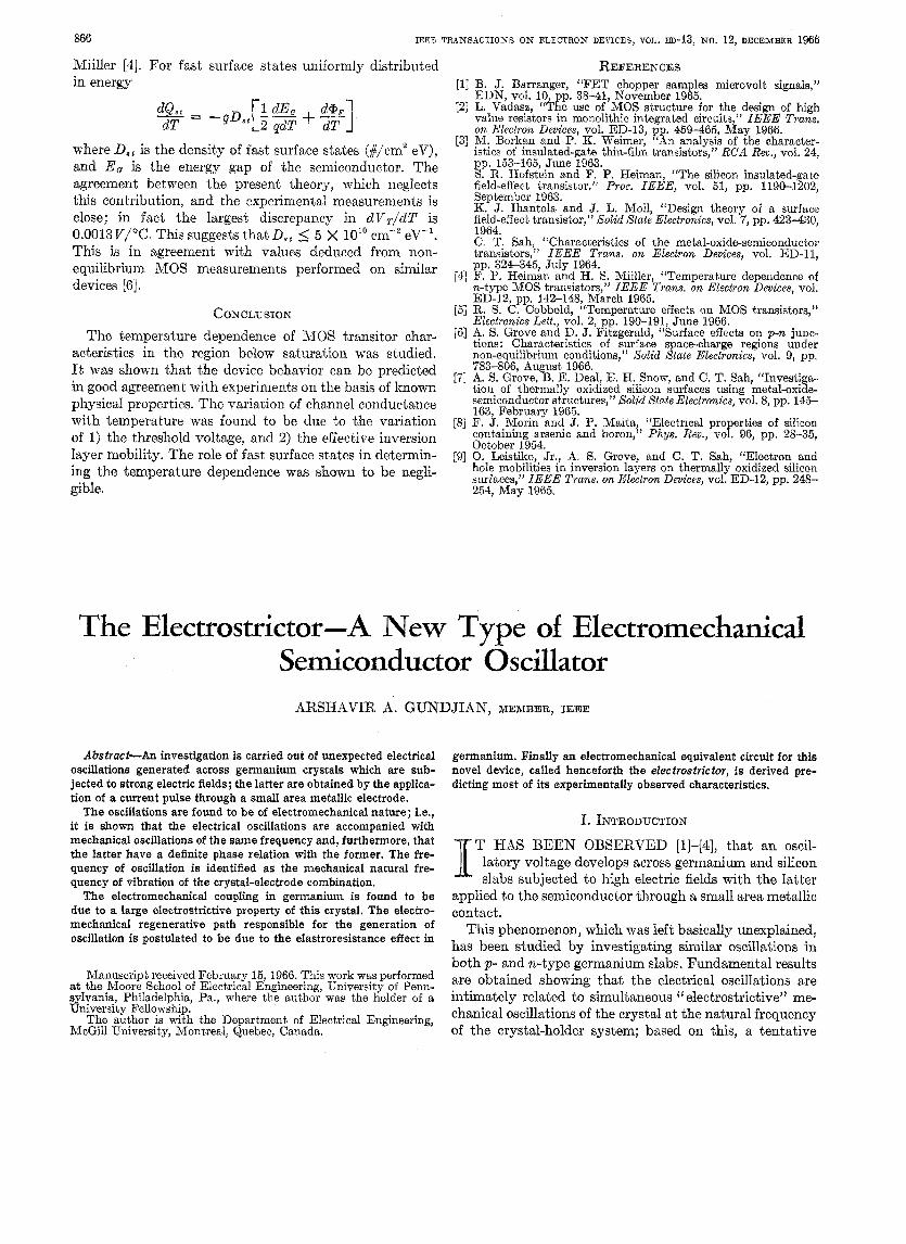
Fig. 1. Connection diagram of the electrostrictor.
regeneration process is described which is believed to provide the explanation for t,he electrical instability causing the oscillations. This novel electromechanical device will be called the electrostrictor.
11. BASIC ELECTROSTRICTOR The electrostrictor consists basically of a rectangular
germanium sample (typically 1 X 2 X 2 mms) subjected to a pulsed electric field (in order t'o avoid overheating) through a small area nonrectifying metallic contact on one side and a large area plated ohmic contact on the other side as shown in Fig. 1. An adjustable impedance 2 shunts the crystal and consists typically of a resistance of a few kilohms in parallel with a capacitance of a fraction of a microfarad. When the conditions of the experiment are satisfactory, sinusoidal oscillations will appear superposed on the normally expected rectangular voltage pulse across the germanium crystal.
111. FUNDAMENTAL CHARACTERISTICS OF THE ELECTROSTRICTOR
A) The frequencies of the oscillations fall in two bands. A lower band of tens of kilocycles and a higher band of several megacycles. The present investigation is, however, concerned with the low frequency oscillations only.
B) The frequency of oscillation is altered very little by large changes in the reactive part of the external impedance 2. However, the amplitude of oscillations is strongly affected when for example, C is increased from 0 to a few microfarads. I n particular, the proper adjust- ment of 2 may change damped oscillations into undamped and even building up oscillations; clearly the dc operating point is kept fixed while 2 is varied.
The percentage modulation of the applied voltage pulse is typically about 10 percent, however, larger depths of modulation of up to 30 percent have been observed.
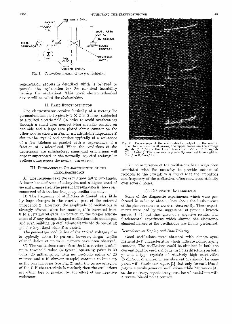
C) The oscillations start when the bias reaches a mini- mum threshold value (a typical operating point is 30 volts, 20 milliamperes, with an electrode radius of 20 microns and a 10 ohm-em sample) continue to build up as the bias increases (see Fig. 2 ) until the turnover region of the I-V characteristic is reached; then the oscillations are either lost or masked by the effect of the negative resistance.
ELECTROSTRICTOR 867
Fig. 2. Dependence of the electrostrictor output on the electric bias. In the three oscillograms, the upper traces are the voltage signals (5 V/div.) the lower traces are the current signals (10 mA/div.). The time axis is positively oriented from right to left ( t = 0 . 5 ms/div.).
D) The occurrence of the oscillations has always been associated with the necessity to provide mechanical freedom t o the crystal; it is found that the amplitude and frequency of t'he oscillations often show good stability over several hours.
IV. DIAGNOSTIC EXPERIMENTS Some of the diagnostic experiments which were per-
formed in order t'o obtain clues about the basic nature of the phenomenon are now described briefly. These experi- ments were lead by the suggestions of previous investi- gators [1]-[4] but they gave only negative results. The fundamental experiment which showed the electrome- chanical nature of the oscillations was finally performed.
Dependence on Doping and Bias Polarity Good oscillations were obtained with almost sym-
metrical I-V characteristics which indicate nonrectifying contacts. The oscillat'ions could be obtained in both the conventional forward and backward bias directions on both p- and n-type crystals of relatively high resistivities (8 ohm-em or more). These observations should be com- pared with Cardona's report [l] that only forward bimed p-type crystals generate oscillations while Muravskii [4], on the contrary, reports the generahion of oscillations with a reverse biased point contact.
868 IEEE TRAKSACTIONS ON ELECTRON DEVICES DECEMBER
> C.R.O. CHANNEL B
- INSULATING BEAD -
PIEZOELECTRIC /TRANSDUCER
*/ C. R.O.
TO ELECTRICAL
CHANNEL A e 4 G e L
CIRCUIT 4-1 CRYSTAL
/ BRASS ELECTRODE
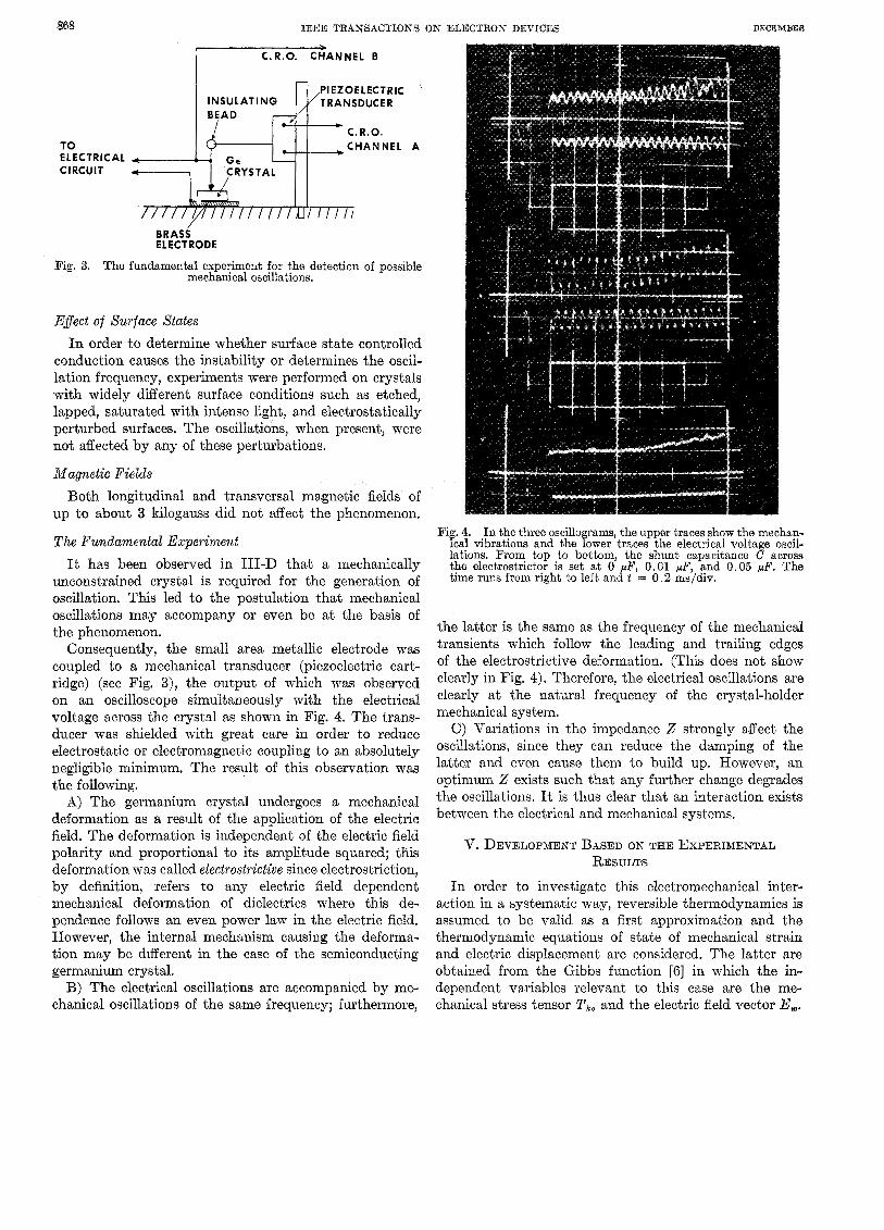
Fig. 3. The fundamental experiment for the detection of possible mechanical oscillations.
Eflect of Xurface Xtates I n order to determine whether surface state controlled
conduction causes the instability or determines the oscil- lation frequency, experiments were performed on crystals with widely different surface conditions such as etched, lapped, saturated with intense light, and electrostatically perturbed surfaces. The oscillations, when present, were not affected by any of these perturbations.
Magnetic Fields Bot>h longitudinal and transversal magnetic fields of
up to about 3 kilogauss did not affect the phenomenon.
The Fundamental Experiment It has been observed in 111-D that a mechanically
unconstrained crystal is required for the generation of oscillation. This led to the postulation that mechanical oscillations may accompany or even be at the basis of the phenomenon.
Consequently, the small area metallic electrode was coupled to a mechanical transducer (piezoelectric cart- ridge) (see Fig. 3), the output of which was observed on an oscilloscope simultaneously with the electrical voltage across the crystal as shown in Fig. 4. The trans- ducer was shielded with great care in order to reduce electrostatic or electromagnetic coupling to an absolutely negligible minimum. The result of this observation was the following.
A) The germanium crystal undergoes a mechanical deformation as a result of the application of the electric field. The deformation is independent of the electric field polarity and proportional t o its amplitude squared; this deformation was called electrostrictive since electrostriction, by definition, refers t o any electric field dependent mechanical deformation of dielectrics where this de- pendence follows an even power law in the electric field. However, the internal mechanism causing the deforma- tion may be different in the case of the semiconducting germanium crystal.
B) The electrical oscillations are accompanied by me- chanical oscillations of the same frequency; furthermore,
Fig. 4. In the three oscillograms, the upper traces show the mechan- ical vibrations and the lower traces the electrical voltage oscil- lations. From top to bottom, the shunt capacitance C across the electrostrictor is set a t 0 pF, 0.01 p F , and 0.05 pF. The time runs from right to left and t = 0 . 2 ms/dlv.
the latter is the same as the frequency of the mechanical transients which follow the leading and trailing edges of the electrostrictive deformation. (This does not show clearly in Fig. 4). Therefore, the electrical oscillations are clearly at the natural frequency of the crystal-holder mechanical system.
C) Variations in the impedance Z strongly affect the oscillations, since they can reduce the damping of the latter and even cause them to build up. However, an optimum 2 exists such that any further change degrades the oscillations. It is thus clear that an interaction exists between the electrical and mechanical systems.
V. DEVELOPMEKT BASED ON THE EXPERIMENTAL RESULTS
In order to investigate this electromechanical inter- action in a systematic way, reversible thermodynamics is a,ssumed to be valid as a first approximation and the thermodynamic equations of state of mechanical strain and electric displacement are considered. The latter are obtained from the Gibbs function [B] in which the in- dependent variables relevant to this case are the me- chanical stress tensor Tks and the electric field vector E,,,.
1966 GUXDJIAN : THE ELECTROSTRICTOR 869
The strain tensor Sij, and electric displacement vector D, are then given by
= SijkeTke 4- T i i m n E r n E n (1 a>
Dn = E n m E m f 2yiimnTiiEm (1b)
where Xiiks are the compliance tensor elements, yiirnn the electrostriction tensor elements, and enm the dielectric tensor elements.
Measurement of Electrostriction in Germanium A major experimental result was the observation of a
large “electrostrictive” deformation (see IV 4-A) in germanium. This being the first such observation, it has been necessary to measure the ma.gnitude of the fourth rank tensor elements describing electrostriction in ger- manium [5], [6]; for a p-type, p = 10 ohm-em crystal, the matrix representation of y with contracted indices is
- 0.33 0.12 0.12 6 0 0
0.12 0.33 0.12 0 0 0
0.12 0.12 0.33 0 0 0
0 ’ 0 0 0.72 0 0
0 0 0 0 0.72 0
0 0 0 0 0 0.72-
X 1o-l’ cm2/volt2. (2)
It is interesting to compare this order of magnitude with that of electrostriction in dielectrics, such as glass, where y is of the order of cm2/volt2.
A sensible dependence of the magnitude of y on the free carrier concentration was detected 161.
Electromechanical Interaction Now, going back to (la), it may be noted that strains
of the order of can be produced, thanks to the y term, by electric fields of the order of few thousands volt/cm; such fields can easily exist in the vicinity of the small area contact of the electrostrictor.
It is clear that a large tensor y explains through (la) the fact that, as the electric field E is applied in the form of a pulse, it genemtes a mechanical strain transient a t both the leading and trailing edges of the mechanical electrostrictive displacement pulse as experimentally ob- served before. However, the nature of the electrome- chanical interaction which would explain the generation of corresponding electrical oscillations is yet to be deter- mined. Equations (la) and (lb) suggest two possibilities.
A. In (lb), the tensor product 2yii,,Em E aii, implies the existence of an equivalent piezoelectric effect (see Reference 161) in the biased (E, # 0) homopolar ger- manium which otherwise has an identically null natural piezoelectricity. Such piezoelectricity suggests a possible interaction between electrons drifting at the speed of sound and the mechanical, electrostrictively generated,
strain waves. However, since the dimensions of the crystals are very small fractions of a mechanical wavelength a t the oscillation frequencies (= X/ lOO at X0 kilocycles), this mechanism is discarded.
B. On the other hand, (la) shows that the crystal is subjected to large strains by the electric field E. It is well known that semiconductors are strongly elasto- resistive [7], [8]; i.e., the resistivity of a semiconductor changes appreciably as it is subjected to a strain. This property is described by a fourth rank tensor M such that the second rank tensor of relative change of resistivity is given by
- ‘e = m : S . P
(3)
Since the electric field E a t a point in a semiconductor is determined by the local resistivity e and the current density J
E = p : J . (4) It is clea’r that an int’eraction exists between the electric field a t a point and the electrostrictive strain at that point through the elastoresistive modulation of the local resistivity. It is important to note that when the electric field E is actually the sum of a constant component E and a small ac component e sin ut , .the ac component of the longitudinal strains are obtained from (la); for longi- tudinal stresses and electric fields (i = j = m = n = k = e = l), and using the contracted indices notation, this becomes
SI = S,,T, + 2yllEoe sin c d ( 3
where the term in e2 is neglected with respect to the E,e term. It is thus clear from ( 5 ) that although electro- striction is a square law effect, .the strains due to in- cremental electric fields and consequently the correspond- ing changes of resistivity are linearly related to the latter. Therefore, feedback can take place at the fundamental operation frequency.
Electromechanical Equivalent Circuit of the .Electrostrictor The electromechanical performance of the germanium
crystal can be described by considering the latter as a two-port network (Fig. 5 ) . The inputs t o the first port are the incremental current i and voltage v at the terminals of the crystal, while the variables at the second port are the incremental mechanical force F and velocity of de- formation of the crystal.
The Z parameters of this electromechanical two-port network are defined by
v = Z,,i + Z12y ( 6 4
F = Z,,i + Z,,y where Zll = ( u / i ) / y = 0 is the electrical input impedance when the mechanical system is clamped. It can be easily shown that, for the configuration of Fig. 6, this cor- responds to the spreading resistance
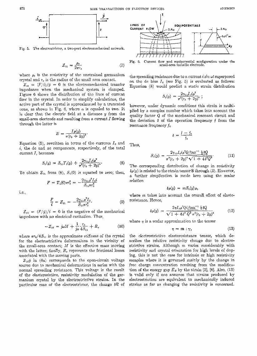
870 IEEE TRANSACTIONS ON ELECTRON DEVICES DECEMEEP.
IPOTENTIALS
Fig. 6. Current flow and equipotential configuration under the small-area metallic electrode.
- Fig. 5. The electrostrictor, a two-port electromechanical network.
z,, = _I 2w0 Po
where po is the resistivity of the unstrained germanium crystal and r o is the radius of the small area contact.
Z,, = ( t ' / i ) / g = 0 is the electromechanical transfer impedance when the mechanical system is clamped. Figure 6 shows the distribution of the lines of current flow in the crystal. In order to simplify calculations, the active part of the crystal is approximated by a truncated cone, as shown in Fig. 6, where a is equaled to two. It is clear that the electric field at a distance y from the small-area electrode and resulting from a current I flowing through the latter is
Equation (9, rewritten in terms of the currents Io and i , the dc and ac components, respectively, of the total current 6, becomes
To obtain Z,, from (8), S,(O) is equated to zero; then,
m.,
ZZz = ( F / y ) / i = 0 is the negative of the mechanical impedance with no electrical excitation. Thus,
where rrro/4X11 is the approximate stiffness of the crystal for the electrostrictive deformations in the vicinity of the sndl-area contact; M is the effective mass moving with the latter; finally, Re represents the frictional losses associated with the moving pa,rts.
Zlzy in (sa) corresponds to the open-circuit voltage source due to mechanical deformations in series with the normal spreading resistance. This voltage is the result of the elastoresistive, resistivity modulation of the ger- manium crystal by the electrostrictive strains. In the particular case of the electrostrictor, the change 6R of
the spreading resistance due to a current i sin w t superposed on the dc bias I , (see Fig. 5 ) is evaluated as follows: Equation (8) would predict a static strain distribution
however, under dynamic conditions this strain is multi- plied by a complex number which takes into account the quality factor Q of the mechanical resonant circuit and the deviation 6 of the operation frequency f from the resonance frequency f o
8 = k h f o
Thus,
The corresponding distribution of change in resistivity 6p(y) is related to the strain tensor S through (3). However, a further simplication is made here using the scalar relation
MY) = mXl(Y)P0 where m takes into account the overall effect of elasto- resistance. Hence,
where q is a scalar approximation to the tensor
7 = m :y, (13)
the electrostrictive elastoresistance tensor, which de- scribes the relative resistivity change due to electro- strictive strains. A.lthough m varies considerably with resistivity and crystal orientation for high levels of dop- ing, this is not the case for intrinsic or high resistivity samples where it is governed mainly by the change in free charge concentration resulting from the modifica- tion of the energy gap E , by the strain [5] , [SI. Also, (13) is valid only if one assumes that strains produced by electrostriction are equivalent to mechanically induced strains as far as changing the resistivity is concerned.
1966 GUNDJIAN THE ELECTROSTRICTOR 871
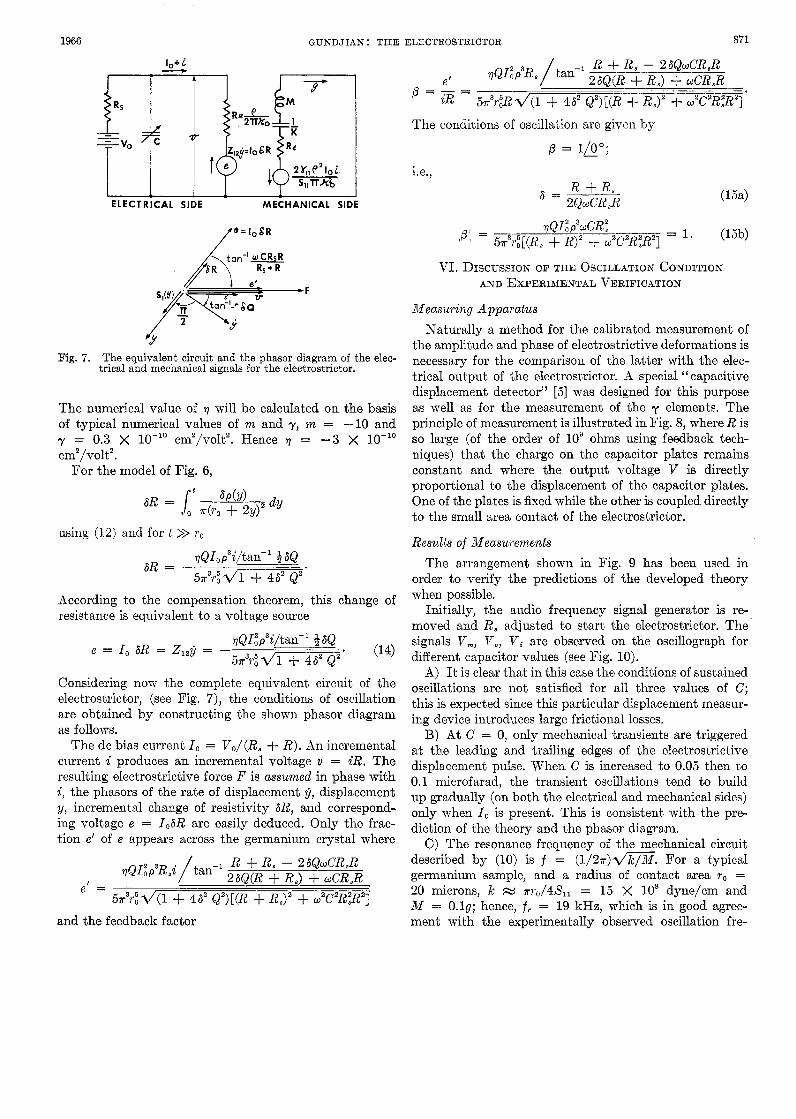
Io+ i -----c
ELECTRICAL SIDE MECHANICAL SIDE
Fig. 7 . The equivalent circuit and the phasor diagram of the elec- trical and mechanical signals for the electrostrictor.
The numerical value of 9 will be calculated on the basis of typical numerical values of m and y, m = -10 and y = 0.3 X lo-'' cm'/volt'. Hence 9 = -3 X lo-'' cm2/voItZ.
For the model of Fig. 6,
using (12) and for t >> yo
pQIop3i/tan-' +SQ 5r3r; c+ 46' Q z
6R = --e
According to the compensation theorem, this change of resistance is equivalent to a voltage source
q&Iip3i/tan-' 8 6Q
57r3ri dl + 46' Q2 e = I, 6R = Z,,y = - * (14)
Considering now the complete equivalent circuit of the electrostrictor, (see Fig. 7), the conditions of oscillation are obtained by constructing the shown phasor diagram as follows.
The dc bias current I, = V,/(R, + R). An incremental current i produces an incremental voltage v = iR. The resulting electrostrictive force F is assumed in phase with i, the phasors of the rate of displacement y , displacement y, incremental change of resistivity 6R, and correspond- ing voltage e = I06R are easily deduced. Only the frac- tion e' of e appears across the germanium crystal where
qQI:p3R.i/tan-' R + R, - 26&wCR,R
5 r 3 r i d ( 1 + 46' Qz)[(R + R,)' + u2CzRiR2] I 26Q(R 4- R,) 4- wCR,R e = -
and the feedback factor
rQlgp3R, /tan-' R + R, - 26&wCR,R e' 268iR i- B e ) i- wCR,R p = - = iR 5n3r;R2/(1 + 46' Q2)[(R+R,)Z + u2CzR?R2]
-~ . "I .
The conditions of oscillat'ion are given by
R + R , 6 = 2QwCR,R
VI. DISCUSSIOK OF THE OSCILLATIOK CONDITION AND EXPERIMENTAL VERIFICA.TION
Measuring Apparatus Naturally a method for the calibrated measurement of
the amplitude and phase of electrostrictive deformations is necessary for the comparison of the latter with the elec- trical output of the electrostrictor. A special "capacitive displacement detector'' [5] was designed for this purpose as well as for the measurement of the y elements. The principle of measurement is illustrated in Fig. 8, where R is so large (of the order of lo9 ohms using feedback tech- niques) that the charge on the capacitor plates remains constant and where the output voltage V is directly proportional to the displacement of the capacitor plates. One of the plates is fixed while the other is coupled directly to the small area contact of the electrostrictor.
Results of Measurements The arrangement shown in Fig. 9 has been used in
order to verify the predictions of the developed theory when possible.
Initially, the audio frequency signal generator is re- moved and R, adjusted to start the electrostrictor. The signals V,, V , , V i are observed on the oscillograph for different capacitor values (see Fig. lo).
A) It is clear that in this case the conditions of sustained oscillations are not satisfied for all three values of C; this is expected since this particular displacement measur- ing device introduces large frictional losses.
B) At C = 0, only mechanical transients are triggered at the leading and trailing edges of the electrostrictive displacement pulse. When C is increased to 0.05 then to 0.1 microfarad, the transient oscillations tend to build up gradually (on both the electrical and mechanical sides) only when I, is present. This is consistent with the pre- diction of the theory and the phasor diagram.
C) The resonance frequency of the mechanical circuit described by (10) is f = ( 1 / 2 7 r ) m . For a typical germanium sample, and a radius of contact area T , = 20 microns, IC M rr0/4SI1 = 15 X 10' dyne/cm and M = 0. lg; hence, f ? = 19 kHz, which is in good agree- ment with the experimentally observed oscillation fre-
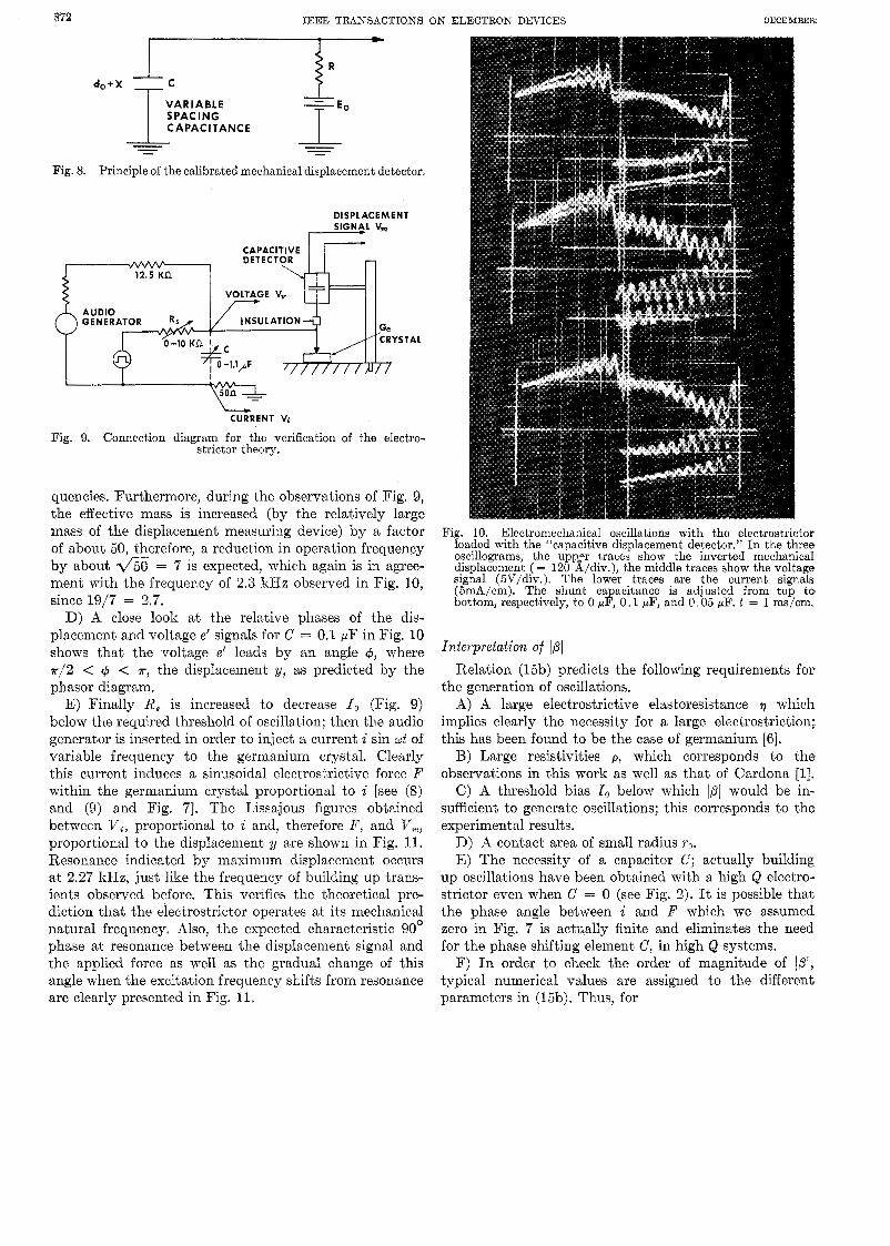
IEEE TRANSACTIONS ON ELECTRON DEVICES DECEMBER.
VARIABLE SPACING CAPACITANCE
Fig. 8. Principle of the calibrated mechanical displacement detector.
DISPLACEMEN1 SIGNAL V, -
CAPACITIVE 1 7 -. . . . . -. . . .
1 12.5 Kn D E T E C T O W n 5 I VOLTAGE V,
F
I I
CURRENT Vi
Fig. 9. Connection diagram for the verification of the electro- strictor theory.
quencies. Furthermore, during the observations of Fig. 9, the effective mass is increased (by the relatively large mass of the displacement measuring device) by a factor of about 50, therefore, a reduction in operation frequency by about 450 = 7 is expected, which again is in agree- ment with the frequency of 2.3 kHz observed in Fig. 10, since 19/7 = 2.7.
D) A close look at the relative phases of the dis- placement and voltage e’ signals for C = 0.1 pF in Fig. 10 shows that the voltage e’ leads by an angle 4, where n / 2 < 4 < T, the displacement y, as predicted by the phasor diagram.
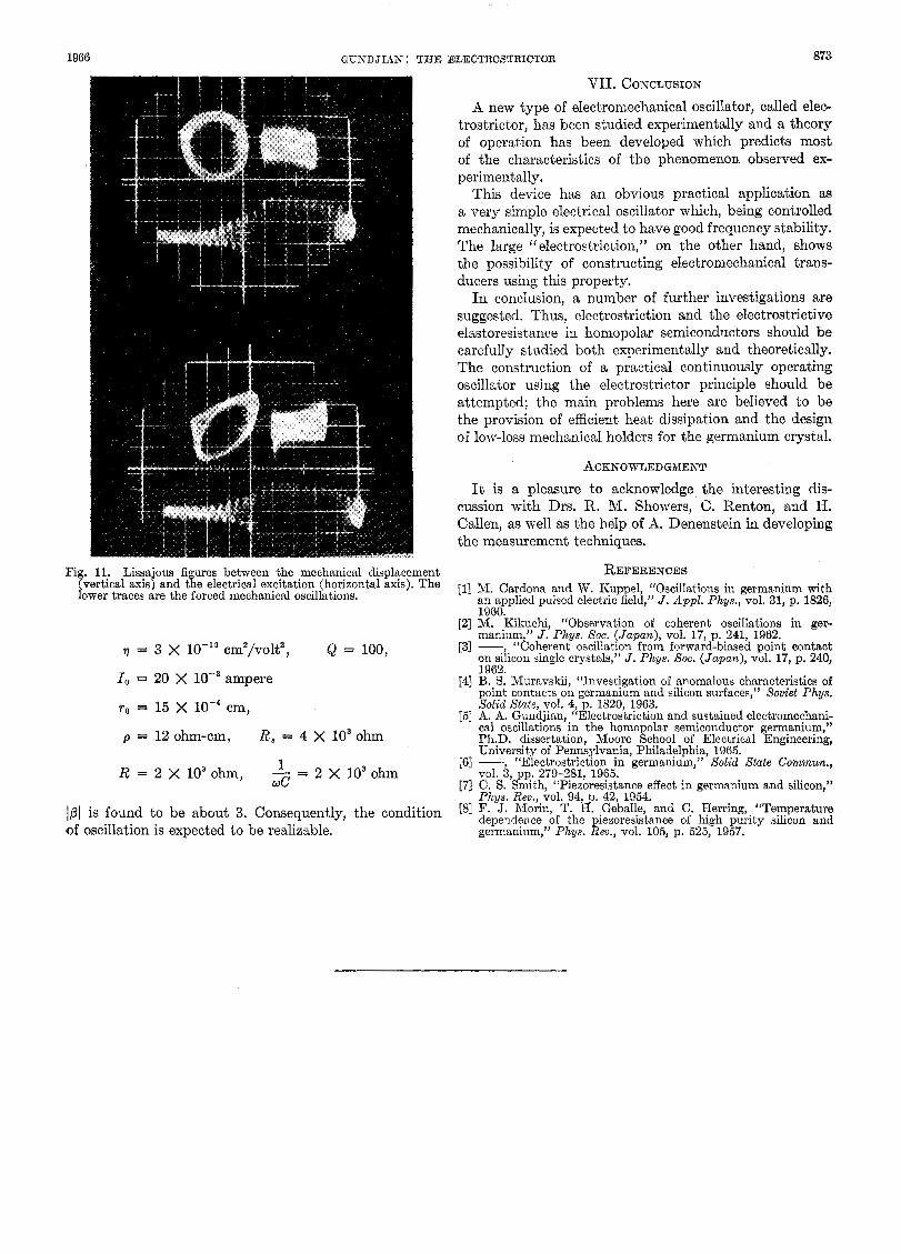
E) Finally R, is increased to decrease I , (Fig. 9) below the required threshold of oscillation; then the audio generator is inserted in order to inject a current i sin at of variable frequency to the germanium crystal. Clearly this current induces a sinusoidal electrostrictive force F within the germanium crystal proportional to i [see (8) and (9) and Fig. 71. The Lissajous figures obtained between Vi, proportional to i and, therefore F , and V,, proportional to the displacement y are shown in Fig. 11. Resonance indicated by maximum displacement occurs at 2.27 kHz, just like the frequency of building up trans- ients observed before. This verifies the theoretical pre- diction that the electrostrictor operates at its mechanical natural frequency. Also, t’he expected characteristic 90Q phase at resonance between the displacement signal and the applied force as well as the gradual change of this angle when the excitation frequency shifts from resonance are clearlv rsresented in Fig. 11.
Fig. 10. Electromechanical oscillations with the electrostrictor loaded with the “capacitive displacement detector.” In the three oscillograms, the uppsr traces show the inverted mechanical
signal. (5Vldiv.). The lower traces are the current signals displacement ( = 120 l/div.), the middle traces show the voltage
(5mA/cm). The shunt capacitance is adjusted from top to bottom, respectively, to 0 pF, 0.1 pF, and 0.05 pF. t = 1 ms/cm.
Interpretation of 101 Relation (15b) predicts the following requirements for
the generation of oscillations. A) A large electrostrictive elastoresistance 7 which
implies clearly the necessity for a large electrostriction; this has been found to be the case of germanium [SI.
€3) Large resistivities p, which corresponds to the observations in this work as well as that of Cardona [l].
C) A threshold bias I , below which I @ ] would be in- sufficient to generate oscillations; this corresponds to the experimental results.
D) A contact area of small radius ro. E) The necessity of a capacitor C; actually building
up oscillations have been obtained with a high Q electro- strictor even when C = 0 (see Fig. 2 ) . It is possible that, the phase angle between i and F which we assumed zero in Fig. 7 is actually finite and eliminates the need for the phase shifting element C, in high Q systems.
F) I n order to check the order of magnitude of [P I , typical numerical values are assigned to the different parameters in (15b). Thus, for
1966 GUNDJIAN : THE ELECTROSTRICTOR 873
Fig. 11. Lissajous figures between the mechanical displacement
lower traces are the forced mechanical oscillations. (vertical axis) and the electrical excitation (horizontal axis). The
11 = 3 X lo-’’ cm2/volt2, Q = 100,
I, = 20 X io-3 ampere
yo = 15 X los4 cm,
p = 12 ohm-cm, R, = 4 X lo3 ohm
R = 2 X IO3 ohm, - = 2 X lo3 ohm 1 w c
1/31 is found to be about 3. Consequently, the condition of oscillation is expected to be realizable.
VII. CONCLUSION A new type of electromechanical oscillator, called elec-
trostrictor, has been studied experimentally and a theory of operation has been developed which predicts most of the characteristics of the phenomenon. observed ex- perimentally.
This device has an obvious practical application as a very simple electrical oscillator which, being controlled mechanically, is expected to have good frequency stability. The large “electrostriction,” on the other hand, shows the possibility of constructing electromechanical trans- ducers using this property.
In conclusion, a number of further investigations are suggested. Thus, electrostriction and the electrostrictive elastoresistance in homopolar semiconductors should be carefully studied both experimentally and theoretically. The construction of a practical continuously operating oscillator using the electrostrictor principle should be attempted; the main problems here are believed to be the provision of efficient heat dissipation and the design of low-loss mechanical holders for the germanium crystal.
ACKNOWLEDGMENT It is a pleasure to acknowledge the interesting dis-
cussion with Drs. R. M. Showers, C. Renton, and H. Callen, as well as the help of A. Denenstein in developing the measurement techniques.
REFERENCES [I] M. Cardona and W. Kuppel, “Oscillations in germaninm with
an applied pulsed electric field,” J . Appl . Phys., vol. 31, p. 1826,
[2] M. .Kiky;hi, “Observation of coherent oscillations in ger- 1960.
[3] -,. “Coherent osclllation from forward-biased point contact manlum, J . Phys. SOC. (Japan), vol. 17, p. 241, 1962.
on slllcon single crystals,” J. Phys. SOC. (Japan), vol. 17, p. 240, 1962.
[4] B. S. Muravskii, “Investigation of anomalous characteristics of point contacts on germanium and silicon surfaces,’’ Soviet Phys.
[5] A. A. Gundjian, ‘LElectrostriction and sustained electromechani- Solid State, vol. 4, p. 1820, 1963.
Ph.D. dissertation, Moore gchool of Electrical Engineering, cal oscillations in the homo olar semiconductor germanium,”
[6] -, “Electrostriction in germanium,” Solid State Commun., University of Pennsylvania, Philadelphia, 1965.
[7] C. S. Smlth, L‘Piezoresistance effect in germanium and silicon,”
[8] F. J. Morin, T. H. Geballe, and C. Herring, “Temperature Phys. Rev., vol. 94, p. 42, 1954.
dependence,pf the piexoresistance of high purity silicon and germanlum, Phys. Rev., vol. 105, p. 525, 1957.
v01. 3, pp: 279-281, 1965.
Related Documents


![Mechanics of Advanced Composite Structures€¦ · a nonlinear oscillator equation in a double-sided clamped micro-beam-based electromechanical reso-nator. Moreover, Fu et al. [22]](https://static.cupdf.com/doc/110x72/5f8f7407fd3f721c8c7e7b45/mechanics-of-advanced-composite-structures-a-nonlinear-oscillator-equation-in-a.jpg)

