THE DESIGN OF SINGLE-EVENT HARDENED BIAS CIRCUITS By Raymond W. Blaine Thesis Submitted to the Faculty of the Graduate School of Vanderbilt University in partial fulfillment of the requirements for the degree of MASTER OF SCIENCE in Electrical Engineering May, 2011 Nashville, Tennessee Approved: W. Timothy Holman Lloyd W. Massengill

Welcome message from author
This document is posted to help you gain knowledge. Please leave a comment to let me know what you think about it! Share it to your friends and learn new things together.
Transcript
THE DESIGN OF SINGLE-EVENT HARDENED BIAS CIRCUITS
By
Raymond W. Blaine
Thesis
Submitted to the Faculty of the
Graduate School of Vanderbilt University
in partial fulfillment of the requirements
for the degree of
MASTER OF SCIENCE
in
Electrical Engineering
May, 2011
Nashville, Tennessee
Approved:
W. Timothy Holman
Lloyd W. Massengill

ACKNOWLEDGEMENTS
I would like to thank The United States Army and The Defense Threat Reduction
Agency for funding this research. This work would not have been possible without the
opportunity, guidance, and support, of my advisor Dr. Tim Holman. Dr Holman’s
endless supply of outstanding ideas and patience are truly amazing.
I would also like to that Dr. Lloyd Massengill and Jeff Kauppila for their support
and help on this project. The other professors that are members of the RER research
group and ISDE at Vanderbilt University have also been a tremendous asset and deserve
my gratitude, thank you.
Brian Olson, Sarah Armstrong, and all the other students involved in research of
single-event effects have been a tremendous resource. In particular, thanks to Brian and
Sarah for helping an Army guy get acclimated and up to speed in a very new and foreign
environment.
Finally, I would like to thank my beautiful wife who already had that hardest job
in the world as an Army spouse. Little did she know that their actually was a job a little
more difficult, an Army graduate student spouse. Her support and encouragement have
been unflappable and it reminds me everyday how lucky I am.

ii
TABLE OF CONTENTS
Page
ACKNOWLEDGMENTS ................................................................................... i
LIST OF FIGURES............................................................................................ iv
Chapter
I. INTRODUCTION ................................................................................... 1
II. RADIATION ENVIRONMENTS AND SINGLE-EVENT
PHENOMENA........................................................................................ 4 4
Introduction ............................................................................................. 4
Radiation Environment and Single-Event-Inducing Particles ................... 6
Galactic Cosmic Rays ........................................................................ 6
Solar Flares and Coronal Mass Ejections............................................ 6
The Trapped Radiation Environment.................................................. 8
Single-Event Mechanisms...................................................................... 12
Charge Generation ........................................................................... 12
Charge Collection ............................................................................ 13
Single-Event Effects .............................................................................. 19
Conclusions ........................................................................................... 20
III. BIAS CIRCUITS................................................................................... 21
Introduction ........................................................................................... 21
Bias Circuit Design................................................................................ 21
A Basic Bias Circuit......................................................................... 22
Bootstrap Current Source ................................................................. 23
Bias Circuit Single-Event Sensitivity ..................................................... 26
Conclusions ........................................................................................... 28
IV. SENSITIVE NODE ACTIVE CHARGE CANCELLATION ................ 29
Introduction ........................................................................................... 29
Circuit Design........................................................................................ 30
Simulation ............................................................................................. 33
Bias-Dependent Single-Event Model................................................ 34
Results ............................................................................................. 35
Conclusions ........................................................................................... 41
V. A RHBD BIAS CIRCUIT UTILIZING SNACC.................................... 44
Introduction ........................................................................................... 44
Circuit Design........................................................................................ 44
iii
Simulation Results ................................................................................. 49
Circuit Design with SNACC.................................................................. 54
Conclusions ........................................................................................... 63
VI. CONCLUSIONS ................................................................................... 66
REFERENCES............................................................................................................. 68
iv
LIST OF FIGURES
Figure Page
II-1. Distribution of spacecraft anomaly versus anomaly type...........................5
II-2. Breakdown of SEU and radiation anomaly records ...................................5
II-3. Galactic cosmic ray particle spectrum as a function of atomic mass ......... 7
II-4. Cosmic rays cascading into a shower of secondary particles
following interaction with earth’s atmosphere...........................................7
II-5. The largest solar flare ever recorded, captured by SOHO satellite .............9
II-6. The motion of particles trapped in the Earth’s magnetosphere...................9
II-7 Diagram of the Van Allen belts...............................................................10
II-8. Particles of the Van Allen belts as a function of Earth radii.....................11
II-9. Contour plot of proton fluxes greater than 10 MeV at a 500 km
altitude during a solar maximum...........................................................11
II-10. Depletion region drift collection from an ion strike.................................15
II-11. The funnel effect; from left to right, (a) a plasma track of free
carriers formed, (b) movement of electrons towards positive bias,
(c) potential drop along the track and redistribution of
equipotential lines down the track...........................................................15
II-12. Illustration of an ion strike on a reversed biased n-p junction..................16
II-13. Illustration of the parasitic bipolar structure............................................17
II-14. Relative size of an electron-hole cloud following a SE strike for a
1µm device vs. a 90 nm device (a) shows that the cloud only
effects a small portion of the drain (b) shows that at a 90 nm
technology node that same SE strike radius structure encompasses
all four terminals of the device................................................................17

v
Figure Page
II-15. Depiction of the results of a 63 MeV proton nuclear event, the
proton interacts with a Silicon nucleus creating energetic
secondary particles, to include a 14 MeV Oxygen ion, proton,
gamma rays, and alpha particles. The oxygen ion traverses six
sensitive volumes and deposits between 30 and 40 fC of charge
in each....................................................................................................18
III-1. A very basic bias circuit consisting of a diode-connected PMOS
transistor and a resistor. ..........................................................................22
III-2. Bootstrap current source schematic with start-up circuit shaded in
gray and mirrored current through a load RLOAD .....................................24
III-3. Establishing a stable operating point in the bootstrap current
reference.................................................................................................26
IV-1. Three different representations of a bias circuit are depicted, (a) is
the depiction for the baseline comparison a simple diode and
resistor, (b) a traditional hardening technique that places a
capacitance on the drain of the diode to mitigate SEE, (c) the
SNACC approach the uses multi-node charge collection and
current mirrors to cancel charge deposited by a SE .................................32
IV-2. (a) Layout design for the SNACC hardened circuit. PMOS
transistors M2 and M3 are interleaved with transistor M4 in
separate wells (dashed lines). The other devices separate the two
wells. M5 and M6 are also interleaved. The layout view is shown
in (b) ......................................................................................................32
IV-3. Block diagram of 6-level metal capacitor. (a) cross-section (b) top-
view, where the area can be specified as parameters (L,W).....................36
IV-4. Fig. IV-3. Drain current of the NMOS device of an inverter
following a 30 MeV-cm2/mg strike. (a) mixed-mode TCAD vs.
traditional double exponential current source. Note the difference
in the “shelf” region. For (b) mixed-mode TCAD vs. bias-
dependent model, note the much better replication of the pulse
shape. .....................................................................................................36
IV-5. The magnitude of the bias voltage point perturbation simulation
results for normal incidence and 60-degree angle strikes for all
three circuits from the unperturbed 600 mV bias point. In both
cases, the voltage excursion improves with SNACC. Note that the
improvement is greater in the angled-strike results..................................36

vi
Figure Page
IV-6. Durations of voltage excursions exceeding 30 mV as a function of
LET for nominal and 60 degree angled strikes on the diode
connected transistor shared with transistor M4 compared with
hardening of a capacitor of equal area and the unhardened circuit.
Again, the figures show an improvement in the SNACC results
over the unhardened and capacitor-hardened circuits with a greater
improvement with angled strikes ............................................................38
IV-7. The magnitude of the bias voltage point perturbation simulation
results for 60-degree angle strikes (left) and the duration of
excursions exceeding 30 mV (left) for 60-degree strikes for
varying LET ...........................................................................................38
IV-8. The magnitude of the bias voltage point perturbation simulation
results for normal incidence and 60-degree angle strikes for all
three circuits from the unperturbed 600 mV bias point. In both
cases, the voltage excursion improves with SNACC. Note that the
improvement is greater in the angled-strike results. The SNACC
device size optimization made it much more favorable than a
capacitor of equal area ............................................................................40
IV-9. Durations of voltage excursions exceeding 30 mV as a function of
LET for nominal and 60 degree angled strikes on the diode
connected transistor shared with transistor M4 compared with
hardening of a capacitor of equal area and the unhardened circuit.
Again, the figures show an improvement in the SNACC results
over the unhardened and capacitor-hardened circuits with a greater
improvement with angled strikes. It is important to note that the
smaller capacitor improves the duration performance of capacitive
hardening................................................................................................40
IV-10. Perturbation amplitude nodal analysis of the SNACC devices
compared to the unhardened circuit. On the left is normal
incidence and the right 60 degree for LETs varying from 10-40
MeV-cm2/mg..........................................................................................42
IV-11. Durations of perturbations exceeding 30 mV for the SNACC
devices compared to the unhardened circuit. On the left is normal
incidence and the right is 60 degree strikes. ............................................43

vii
Figure Page
V-1. (a) Circuit diagram of the bootstrap current source. The startup
circuitry is highlighted gray and has minimal impact during normal
circuit operation. (b) The SNACC hardening technique applied to
the node shared between M2 and M4 with the relative W/L ratios
labeled....................................................................................................45
V-2. (a) SE perturbation amplitudes from a nodal analysis of circuit
from fig. V-1 for normal incidence (left) and 60-degree (right)
strikes. (b) SE perturbation durations outside 10% of bias point for
normal incidence (left) and 60-degree (right) strikes for varying
LET........................................................................................................46
V-3. (a) The amplitude and duration of perturbations seen on a mirrored
node following 60-degree SE strikes to device M4 for vary (W/L)
ratios of M8 and M9. (b) The amplitude and duration of
perturbations seen on a mirrored node following 60-degree strikes
on the drain of M2 for different size (W/L) devices. M10 and M11
with varying LET ...................................................................................48
V-4. A comparison of five circuits, baseline (fig. V-1(a)), baseline
hardened with a capacitor of equal area, devices M4 and M3
interleaved, devices M4 and M3 interleaved with a capacitor of
equal area, and SNACC for both normal incidence (left) and 60-
degree (right) SE strikes to device M4 with varying LET. (a)
Perturbation amplitude (b) Perturbation duration ....................................51
V-5. A comparison of five circuits, baseline (fig. V-1(a)), baseline
hardened with a capacitor of equal area, devices M2 and M1
interleaved, devices M2 and M1 interleaved with a capacitor of
equal area, and SNACC for both normal incidence (left) and 60-
degree (right) SE strikes to device M2 with varying LET. (a)
Perturbation amplitude (b) Perturbation duration ....................................53
V-6. A nodal analysis of the bootstrap bias circuit. Shown in gray are
the values for perturbation amplitude (left) and duration (right)
following 60-degree strikes for varying LET. These are the same
values from Fig. V-2. Those gray lines are now represented in the
same colors as Fig. V-2 with SNACC applied. The M3 drain is
now the most sensitive junction, with a reduction of approximately
400 mV and 16 ns at an LET of 40 MeV-cm2/mg compared to the
unhardened circuit. .................................................................................55

viii
Figure Page
V-7. Percent mismatch of current (y-axis) between devices M3 and M4
in the bootstrap design as a function of channel length (x-axis).
The circuit has almost no degradation in matching down to 0.5 µm
channel length ........................................................................................55
V-8. Nodal analysis of the bootstrap current source with .5 µm channel
lengths depicting the perturbation amplitudes (a) and durations
exceeding a 10% bias threshold (b) as a function of LET........................57
V-9. SE Perturbation amplitudes (left) and durations exceeding a 10%
threshold (right) following 60-degree strikes to device M4 for
different size (W/L) devices M8 and M9 with varying LET ....................59
V-10. SE Perturbation amplitudes (left) and durations exceeding a 10%
threshold (right) following 60-degree strikes to device M2 for
different size (W/L) devices M10 and M11 with varying LET ................59
V-11 Layout view of SNACC applied to the bootstrap current source.
The SNACC devices are shown in red (PMOS) and yellow
(NMOS), while the current source devices are blue (PMOS) and
gray (NMOS) .........................................................................................60
V-12. Waveform for a 40 MeV-cm2/mg strike to M2. The three
circuits depicted are the baseline (brown), baseline hardened
with a capacitor (red) and the baseline hardened by SNACC
(blue)......................................................................................................60
V-13. Perturbation amplitudes following normal incidence (left) and 60-
degree angled (right) SE strike to device M4. There are three
circuits being compared the baseline, the baseline hardened with a
capacitor of equal area to the SNACC circuit, and the SNACC
circuit for varying LET...........................................................................61
V-14. Perturbation durations exceeding a 10% bias threshold following
normal incidence (left) and 60-degree angled (right) SE strike to
device M4. There are three circuits being compared the baseline,
the baseline hardened with a capacitor of equal area to the SNACC
circuit, and the SNACC circuit for varying LET .....................................61

ix
Figure Page
V-15. Perturbation amplitudes following normal incidence (left) and
60-degree angled (right) SE strike to device M2. There are
three circuits being compared the baseline, the baseline
hardened with a capacitor of equal area to the SNACC circuit,
and the SNACC circuit for varying LET.................................................63
V-16. Perturbation durations exceeding a 10% bias threshold following
normal incidence (left) and 60-degree angled (right) SE strike to
device M2. There are three circuits being compared the baseline,
the baseline hardened with a capacitor of equal area to the SNACC
circuit, and the SNACC circuit for varying LET .....................................63
V-17. A nodal analysis of the bootstrap circuit with SNACC applied. On
the left are perturbation amplitudes and on the right the durations
for 60-degree strikes. The original values for the drains of M4 and
M2 are left in gray for comparison..........................................................65

1
CHAPTER I
INTRODUCTION
A growing concern in the microelectronic industry is the effect of ionizing
radiation. Ionizing particles exist not only in the space environment, but also in the
ground-level terrestrial environment, generating free carriers through their interactions
with semiconductor devices. These free carriers then can be collected via various
mechanisms at different device nodes in an integrated circuit (IC), resulting in
undesirable circuit response depending on the circuit, the amount of charge deposited,
and how much of the subsequent charge is collected. An ionizing particle interacting
with a semiconductor in this manner is called a single-event (SE). The results of these
SEs are typically called single-event effects (SEE), and an effect of particular concern for
this work is a single-event transient (SET). A SET is an asynchronous signal that can
propagate through a circuit causing a variety of undesirable responses. In digital circuits,
an SET can propagate to a latch. If it meets certain set-up and hold times, then the
erroneous signal can be latched and become a single-event upset (SEU). In analog and
mixed-signal applications, on the other hand, the definition of a SEU is more complicated
and depends on the circuit topology
Bias circuits (e.g. current sources) provide essential global signals in analog and
mixed-signal design. Ideally, a bias circuit should be invariant over operating conditions
such as temperature, output load, and supply voltage. Given the effort and cost required
to implement a high-performance precision bias current source, current mirrors are

2
typically used to replicate a single stable current throughout an entire integrated circuit.
Consequently, a single-event (SE) strike to a critical bias circuit node can have wide-
ranging global effects throughout the IC. A hardened precision bias current source is
essential to prevent multiple errors from disrupting the operation of an entire integrated
system.
The effect of an SE strike to a bias circuit will be discussed in this work through
three examples. These examples will show that a SE to a bias circuit can manifest itself
in three very different ways: micro-second long transient pulses in an analog-to-digital
converter operating at gigahertz frequencies, millisecond-long transients on the output of
a LM6144 operational amplifier, and a near doubling in operation frequency in the output
of a voltage-controlled oscillator [1, 2, 3].
This thesis presents a novel radiation-hardened-by-design (RHBD) technique that
takes advantage of the multi-node charge collection mechanism and employs it through a
balancing and mirroring circuit topology to mitigate the effects of a single-event strike.
This technique, called sensitive node active charge cancellation (SNACC), can be
applied to harden critical nodes in analog and mixed-signal circuits. In this work, the
SNACC technique is applied to a bias current source topology typical of the designs used
throughout industry.
The SNACC technique and the proposed bias circuit are transportable across
technology nodes and can be implemented by any standard foundry. The hardened bias
circuit is compared with a traditional capacitive hardening technique to quantify its
usefulness and performance. The SNACC hardening technique is verified using
simulations in a 90-nm CMOS process. The performance of these bias circuits will be

3
characterized by the magnitude and duration of the SET following a SE strike. It will be
shown that sensitive-node active charge cancellation can reduce both metrics by nearly
75% when compared to capacitive hardening alone.

4
CHAPTER II
RADIATION ENVIRONMENTS AND SINGLE-EVENT PHENOMENA
Introduction
The types of ionizing particles, their energies, and particle abundance in an
environment must all be considered when designing a microelectronic system. The
characteristics of a particle and how it interacts with the semiconductor material can
cause many different effects, including displacement damage (DD), total ionizing dose
(TID), prompt dose (dose rate), and single-event effects (SEE). The continued push by
the commercial industry for reduced core voltages, lower current devices, smaller feature
sizes, and higher packing densities makes devices and circuits more susceptible to upset
from single event (SE) charge, and makes SEE mitigation more important for space and
terrestrial applications [4]. Fig. II-1 shows that SEE accounts for 28% of all spacecraft
anomalies, which include electrostatic discharge (ESD), non-SEE radiation damage,
plasma and micrometeoroid impacts, and uncategorized solar energy particle effects [5,
6]. Fig. II-2 shows that of all radiation effects observed, 84% are attributed to single-
event upsets (SEU) [5, 6]. Single-event effects will be the focus of this work, but
references for displacement damage [7], dose rate [8], and TID [9] are provided for the
interested reader.

5
Fig. II-1. Distribution of spacecraft anomaly versus anomaly type [5, 6].
Fig. II-2. Breakdown of SEU and radiation anomaly records [5, 6].

6
Radiation Environment and Single-Event Inducing Particles
The primary contributors to the space radiation environment are galactic cosmic
rays (GCR), solar flares, and trapped particles. These different influences can interact
with semiconductor devices and cause undesirable effects.
Galactic Cosmic Rays
The origin of GCRs is unknown and a current area of research, but it is believed
that they originate outside our solar system and are the remnants from nova and
supernova explosions. Ions that compose these GCRs are almost all known and are
depicted in Fig. II-3 [10]. As Fig. II-3 shows, the major players are H+ and ! (He
2+)
particles representing 83% and 13% of those rays respectively. Of the GCR spectra, 3%
are composed of high-energy electrons and 1% of heavy ions (z > 2). While heavy ions
make up only a small portion of the GCR spectra, they play an important role in SEE
because they can penetrate shielding.
There are two other subsets of cosmic rays that are of interest to SE response of
circuits: solar cosmic rays (SCR) and terrestrial cosmic rays (TCR). SCRs originate from
tremendous explosions on the sun and consist mostly of protons, but also contain helium
and other heavier elements. TCRs originate within the Earth’s atmosphere and are the
byproduct of these other rays with the atmosphere itself. Fig. II-4 illustrates that TCRs
are composed off mostly of protons, neutrons, pions, muons, electrons, and photons [11].
Solar Flares and Coronal Mass Ejections
Solar flares and coronal mass ejections are sudden, frequent, and intense
emissions of gas and plasma emitted from the sun’s atmosphere. The sun has an average

7
Fig. II-3. Galactic cosmic ray particle spectrum as a function of atomic mass [10].
Fig. II-4. Cosmic rays cascading into a shower of secondary particles following
interaction with earth’s atmosphere [11].

8
solar cycle of 11 years with 7 years of high activity.
Normally the most energetic and frequent flares occur during this 7-year period.
There are two primary types of flares: gradual eruptions and rapid intense bursts.
Gradual eruptions can last several days and are characterized as being rich in protons
ranging in energies from 30 to 100 MeV. Intense bursts, on the other hand, tend to only
last for hours, but are characterized by energies on the order of 100 GeV.
Radiation from solar flares can encompass almost the entire electromagnetic
spectrum, to include radio waves, x-rays, and gamma rays, and can increase the flux of
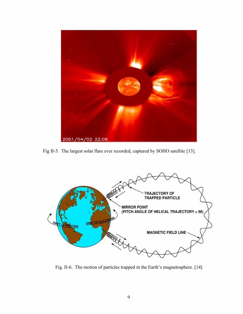
cosmic rays that penetrate the earth’s magnetosphere [12]. The largest solar flare ever
recorded, depicted in Fig. II-5, was captured by the Solar and Heliosphere Observatory
(SOHO) satellite on April 2, 2001 as a CME [13]. This CME sent particles into space at
approximately 7.2 million kilometers per hour and caused radio blackouts on the sunlit
side of the earth.
The Trapped Radiation Environment
A large concern for electronics destined to orbit the earth is the trapped radiation
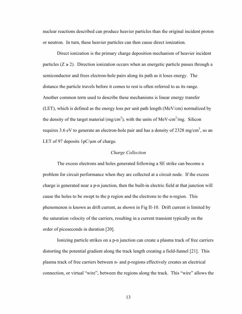
environment. Geomagnetic field lines can trap particles near the Earth’s atmosphere.
Particles trapped by these field lines move in a spiral fashion around the lines tightening
towards the poles, fig II-6 [14]. The Van Allen belts are a result of particles being
trapped along these field lines [15]. The two primary zones within the Van Allen belts
are commonly referred to as the inner and outer belt, as shown in Fig. II-7. The inner belt
is at approximately 2.5 Earth radii (1 radii = 6380 km) and the outer belt is at
approximately 6 Earth radii.
The composition of the particles in these belts is also quite different. The outer
9
Fig II-5. The largest solar flare ever recorded, captured by SOHO satellite [13].
Fig. II-6. The motion of particles trapped in the Earth’s magnetosphere. [14]

10
Fig. II-7. Diagram of the Van Allen belts [15].
belt is composed mostly comprised of electrons with some protons from solar flare
events. The inner belt, on the other hand, is composed mostly protons with some
electrons [16, 14]. Fig II-8 shows a breakdown of the particle composition of the belts as
a function of earth radii [14]. Other belts may appear during intense solar activity, but
they are temporary in nature.
The high fluxes of protons in the lower belt make them the main concern for
SEEs of spacecraft in near-Earth (1.5-3.5 radii) and polar orbits. The protons in this
range can have energies that range anywhere from keV to MeV. The inner belt also
contains a phenomenon referred to as the South Atlantic Anomaly (SAA), located off the
coast of South America. Within the SAA, proton fluxes greatly increase at an altitude of
less than 1000 km. The South Atlantic Anomaly is a result of the tilt and shift of the
Earth’s geomagnetic and rotational axis relative to each other. This relationship causes a

11
Fig. II-8. Particles of the Van Allen belts as a function of Earth radii [14].
Fig. II-9. Contour plot of proton fluxes greater than 10 MeV at a 500 km altitude during
a solar maximum [14].

12
displacement of the magnetic field from the center (off the coast of Argentina), as
depicted in Fig II-9.
Single-Event Mechanisms
Heavy ions, alpha particles, and trapped protons from the environments
previously discussed can all cause damage to semiconductor devices. The basic
mechanism for this is that an ionizing particle loses energy in the semiconductor material
via Coulombic interactions, creating a dense cloud of electron-hole pairs in its wake. The
electron-hole pairs are collected at circuit nodes and can cause undesirable circuit
behavior.
Charge Generation
Ionizing radiation generates charge in a semiconductor via two primary
mechanisms: indirect and direct ionization. Indirect ionization is the result of nuclear
interactions between an energetic particle and the struck material, resulting in ionization
by secondary particles. The incident particle in this case is a low mass particle such as a
proton or neutron. The proton or neutron strike can cause some very significant upset
rates due to inelastic collisions with a target nucleus [17, 18].
Lighter particles striking silicon can create nuclear reactions such as inelastic
collisions producing a silicon recoil or alpha/gamma particle emission and recoil of the
daughter nucleus. An example of the latter is when silicon emits an alpha particle and a
recoiling daughter magnesium nucleus. Another type of nuclear reaction is a spallation
reaction where the target nucleus is broken into two fragments. An example of this is
silicon breaking into carbon and oxygen ions, both of which can recoil [19]. Any of the
13
nuclear reactions described can produce heavier particles than the original incident proton
or neutron. In turn, these heavier particles can then cause direct ionization.
Direct ionization is the primary charge deposition mechanism of heavier incident
particles (Z " 2). Direction ionization occurs when an energetic particle passes through a
semiconductor and frees electron-hole pairs along its path as it loses energy. The
distance the particle travels before it comes to rest is often referred to as its range.
Another common term used to describe these mechanisms is linear energy transfer
(LET), which is defined as the energy loss per unit path length (MeV/cm) normalized by
the density of the target material (mg/cm3), with the units of MeV-cm
2/mg. Silicon
requires 3.6 eV to generate an electron-hole pair and has a density of 2328 mg/cm3, so an
LET of 97 deposits 1pC/µm of charge.
Charge Collection
The excess electrons and holes generated following a SE strike can become a
problem for circuit performance when they are collected at a circuit node. If the excess
charge is generated near a p-n junction, then the built-in electric field at that junction will
cause the holes to be swept to the p region and the electrons to the n-region. This
phenomenon is known as drift current, as shown in Fig II-10. Drift current is limited by
the saturation velocity of the carriers, resulting in a current transient typically on the
order of picoseconds in duration [20].
Ionizing particle strikes on a p-n junction can create a plasma track of free carriers
distorting the potential gradient along the track length creating a field-funnel [21]. This
plasma track of free carriers between n- and p-regions effectively creates an electrical
connection, or virtual “wire”, between the regions along the track. This “wire” allows the
14
electrons to move towards and the holes away from positively charged n-regions. The
spreading resistance along the length of the “wire” results in a voltage drop and a
collapse in the junction’s electric field. This effect takes the potential (initially isolated
across the depletion region) and spreads it down the plasma track, exposing carriers
initially outside the depletion region to its electric field [20]. This effect increase the
amount of charge collected via drift, as depicted in Fig II-11. As devices scale further
below 100 nm, this process becomes more complex because the plasma wire length is on
the order of device size [22, 23].
Charge that is not collected via drift may still be collected through diffusion.
Diffusion occurs when charge is generated from an ionizing particle within a diffusion
length of a junction. A struck node, a neighboring node, or multiple nodes within that
length can therefore collect charge. Diffusion collection takes longer than drift collection
and can be on the order of hundreds of picoseconds to nanoseconds. The fact that this
collection takes longer makes the free carriers more susceptible to recombination
mechanisms, therefore reducing the total amount of charge that is collected [24]. Fig. II-
12 depicts charge collection and recombination in a reversed biased n-p junction [25],
with the initial prompt collection through drift and then subsequent collection from
diffusion.

15
Fig. II-10. Depletion region drift collection from an ion strike [20].
Fig. II-11. The funnel effect; from left to right, (a) a plasma track of free carriers formed,
(b) movement of electrons towards positive bias, (c) potential drop along the track and
redistribution of equipotential lines down the track [20].

16
Two other very important mechanisms that play a role in charge collection are ion
shunt effects and parasitic bipolar effects. The ion shunt effect occurs when an ion
strikes through two proximal junctions creates a dense carrier plasma between them. If
these two junctions are of the same type, this path can conduct current and increase the
total amount of charge collected at the node.
The parasitic bipolar effect occurs primarily after SE strikes to PMOS devices in
n-wells. The collection of SE deposited electrons in the n-well reduces its potential. This
potential collapse with extra carriers in the substrate turns on the parasitic PNP bipolar
device between the drain (collector), body (base), and source (emitter). This effect
(depicted in Fig. II-13) can greatly increase the amount of total charge collected
following a SE strike.
Fig. II-12. Illustration of an ion strike on a reversed biased n-p junction [25].

17
Fig. II-13. Illustration of the parasitic bipolar structure [25].
Fig. II-14. Relative size of an electron-hole cloud following a SE strike for a 1µm device
vs. a 90 nm device (a) shows that the cloud only effects a small portion of the drain (b)
shows that at a 90 nm technology node that same SE strike radius structure encompasses
all four terminals of the device [22].

18
Charge sharing is another charge collection effect that is becoming more
important as devices scale further below 90 nm. The driving mechanism behind charge
sharing or multi-node charge collection is depicted in Fig. II-14 [22]. As devices sizes
decrease and packing densities increase, more devices become susceptible to the electron-
hole cloud created following a SE strike. The width of the electron-hole cloud is
independent of the technology node, so a cloud that previously only encompassed a
single drain may now cover several devices. This charge sharing effect can have many
ramifications, including potential modulation of multiple junctions and current transients
at multiple junctions. Another mechanisms leading to charge sharing is depicted in Fig
II-15 [26].
Fig. II-15 Depiction of the results of a 63 MeV proton nuclear event, the proton interacts
with a Silicon nucleus creating energetic secondary particles, to include a 14 MeV
Oxygen ion, proton, gamma rays, and alpha particles. The oxygen ion traverses six
sensitive volumes and deposits between 30 and 40 fC of charge in each [26].

19
In this work it was demonstrated that nuclear reactions from an incident 63 MeV
proton and a silicon nucleus could create secondary particles like a 14 MeV oxygen ion,
proton, gamma rays, and alpha particles. The simulations showed that the oxygen ion
would traverse six sensitive volumes of silicon and deposit between 30 and 40 fC in each
volume [26]. Charge sharing across multiple junctions from a single ion strike can create
multiple-bit-upsets (MBUs), which are expected to become increasingly critical to future
device and circuit single-event characterizations.
Single-Event Effects
Charge collection at circuit nodes can result in a variety of effects. Some SEEs
can create catastrophic system failures, referred to as hard errors. Examples include
single-event burnout (SEB), single-event gate rupture (SEGR), and single-event latchup.
While important, hard errors are not the focus of this research, and interested readers can
find additional detail in the provided references [19, 27, 28, 29].
Single-event strikes in CMOS devices also create temporary glitches or errors and
are referred to as soft errors. One type of soft error of particular interest for analog and
mixed-signal applications is the single-event transient (SET), an unwanted asynchronous
electrical pulse that can propagate through the signal path causing unintended circuit
behavior.
In a digital circuit, a SET can become a single-event upset (SEU) if the transient
alters a latched logic state (i.e. a “0” becomes a “1”, or a “1” becomes a “0”). The
perturbation of multiple nodes leading to multiple mislatched bits is referred to as a

20
multiple-bit upset (MBU). SEUs and MBUs can lead to a circuit error if the incorrectly
latched bit or bits reach an output node, or corrupt an internal state machine or program.
Characterization of SE induced errors in analog and mixed-signal design can be
more difficult than errors in digital circuits, as no standard error metric exists for analog
and mixed-signal circuits. The effect of the strike and transient are dependent on the
circuit topology, type, and mode of operation.
Conclusions
This chapter presents an overview of the space radiation environment and its
effects on microelectronic circuits. Particular detail was paid to charge generation and
collection mechanisms in silicon based devices. The overall impact of these mechanisms
leading to SEEs and SEUs was discussed. The remainder of this thesis will focus on the
mitigation of those effects in analog and mixed-signal design, with a focus on the
hardening of bias circuitry.

21
CHAPTER III
BIAS CIRCUITS
Introduction
This chapter provides a background on current mirrors, current sources, and
current sinks, with the goal of facilitating their design and analysis for radiation
environment applications. Particular detail will be paid to the bootstrap current sources
that are the basis of this research.
Bias Circuit Design
Bias circuits (e.g. voltage sources and current sources) are fundamental building
blocks used extensively in analog and mixed-signal ICs. Bias circuits typically combine
diodes, resistors, BJTs, and/or MOSFETs to generate stable voltages and/or currents for
other subcircuits on an IC. For example, an operational amplifier uses current sources as
active loads for amplification stages, and to force the amplifier to operate at a quiescent
DC point inside its active linear range. Properly designed current sources should be
relatively independent of supply voltage, temperature, load resistance, and load voltage.
A high-performance current source will provide good precision, good repeatability, high
temperature stability, low long-term drift, high output impedance, high bandwidth, and a
large dynamic output range.
The use of current sources as bias circuits is not a new concept by any means, as
the concept predates the modern IC by several decades with the design of vacuum tube
electronics. The design of high-performance bias circuits for monolithic analog ICs was

22
an active area of research from the mid-1960s to the mid-1980s, and to a lesser extent
continues to this day. The early pioneers and innovators in this area of analog circuit
design worked for companies such as Philbrick, Texas Instruments, Fairchild
Semiconductor, National Semiconductor, GE, Analog Devices, RCA, Motorola, and
many others.
Bias circuits based on current sources can be classified into two types. A current
source usually refers to a circuit connected between a positive supply rail and a load. A
current sink typically refers to a circuit connected between the load and a negative
voltage or ground. A current mirror provides multiple current sources/sink outputs that
mirror a reference current source or sink with predefined output ratios.
A Basic Bias Circuit
One of the most basic topologies for a bias circuit is a current source composed of
a diode-connected MOSFET connected to a drain resistor, as shown in Fig. III-1. This
circuit has a single sensitive node to SE strikes, making it a useful starting point for the
analysis in chapter IV.
Fig. III-1. A very basic bias circuit consisting of a diode-connected PMOS transistor and
a resistor.
VG VS
VD
ID

23
The reference current (i.e. the drain current) provided by the circuit in Fig, III-1
can be derived using the PMOS saturation current equation (III-1), neglecting short
channel effects. The gate and the drain of the MOSFET are tied together, forcing the
device to operate in saturation mode.
!
ID
=1
2k(W
L)(V
SG" V
T)2
ID
=1
2k(W
L)(V
DD" I
DR " V
T)2
In equation III-2, VS is replaced with VDD and VG is replaced with VD = IDR. This
equation shows that the reference (drain) current has a square law dependence on both the
power supply voltage VDD and the resistance R.
A standard technique for modern IC design is to mirror the current from a single
reference circuit into multiple outputs as needed at other subcircuits on the IC. However,
the simple diode-resistor current source is a poor choice for the reference circuit, due to
the significant dependencies of the supply voltage and drain resistance value on the
reference current value. Furthermore, the PMOS threshold voltage and the resistance
value R are temperature dependent, resulting in a temperature-dependent drain current as
given in equation III-2. All of these dependencies would be reflected in the mirrored
current throughout the IC. Consequently, the reference current must be generated using a
high-performance circuit that reduces the effects of these dependencies.
Bootstrap Current Source
A current source that is independent of loading, temperature, and fluctuations in
supply voltage is the ultimate goal. One method to minimize or eliminate the supply
voltage dependence is to use a current through a transistor to create a voltage that in turn
(III-1)
(III-2)

24
sets the current in the transistor. The self-generated current and voltage would then be
independent of the supply voltage. Fig. III-2 is an example of this technique [30]. This
circuit is sometimes called a VT-referenced current source, but more commonly is
referred to as a bootstrap current source. In this schematic, the mirroring of transistors
M3 and M4 force currents I1 and I2 to be equal. Since I1 is also the drain current of M1, it
generates the voltage drop VGS1. I2 is also the drain current of M2 and flows through
RBIAS, creating the voltage I2RBIAS. The gate of M1 is connected to the source of M2, so
VGS1 is set equal to I2RBIAS.
Fig. III-2. Bootstrap current source schematic with start-up circuit shaded in gray and
mirrored current through a load RLOAD [30].

25
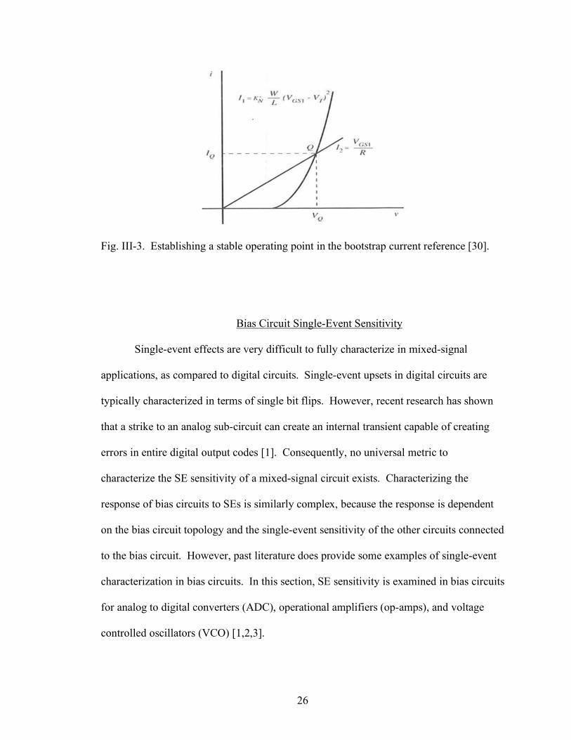
Neglecting channel-length modulation effects, the MOSFET square law equation
can be used to substitute for VGS1, resulting in equation III-3. Substituting # for K’(W/L)
and rearranging terms results in the expression for the quiescent bias current IQ as shown
in equation III-4 [30].
!
I 2R =VT1 + (2I1L1KN' W1
)
1
2
I Q = I 2 =V
T1
R+
1
"1R2
+1
R(2V
T1
"1R+
1
"12R2)
1
2
These equations make it apparent that (to the first order) I1 and I2 are independent of
power supply voltage VDD. However, plotting Equation III-4 in Fig. III-3 shows that a
second operating point exists where I1 and I2 equal zero. A startup circuit is necessary to
keep this circuit operating at the non-zero equilibrium point. The circuitry in the gray
shaded box of Fig. III-2 serves as a startup circuit. If the circuit is at the wrong
equilibrium point then I1 and I2 are equal to zero, and the source voltage of M6 will be
zero. In this case transistor M6 will provide a current to M1, generating voltage VGS1 and
forcing the bootstrap circuit to turn on. As the circuit approaches the desired equilibrium
point, the source voltage of M6 will increase, decreasing its drain current. At the desired
bias point, transistor M6 will be turned off and no longer affect the bootstrap circuit’s
operation.
III-3
III-4
26
Fig. III-3. Establishing a stable operating point in the bootstrap current reference [30].
Bias Circuit Single-Event Sensitivity
Single-event effects are very difficult to fully characterize in mixed-signal
applications, as compared to digital circuits. Single-event upsets in digital circuits are
typically characterized in terms of single bit flips. However, recent research has shown
that a strike to an analog sub-circuit can create an internal transient capable of creating
errors in entire digital output codes [1]. Consequently, no universal metric to
characterize the SE sensitivity of a mixed-signal circuit exists. Characterizing the
response of bias circuits to SEs is similarly complex, because the response is dependent
on the bias circuit topology and the single-event sensitivity of the other circuits connected
to the bias circuit. However, past literature does provide some examples of single-event
characterization in bias circuits. In this section, SE sensitivity is examined in bias circuits
for analog to digital converters (ADC), operational amplifiers (op-amps), and voltage
controlled oscillators (VCO) [1,2,3].

27
In 2007, Kruckmeyer, et al., published a paper that presented a new analysis
technique for determining the SEU sensitivity of high frequency ADCs [1]. The ADCs
were exposed to a 4.5 MeV/nucleon ion beam with a spectrum of different ions and
associated energies. Unusually long single-event transients on the order of 1.7 µs were
observed during this testing. Because the ADC was operating at 1.2 gigasamples per
second (GS/s), an observed 1.7 µs transient correlated to over 2000 missed samples.
Extensive bench testing was conducted to determine the reason for these long transients,
with the cause traced back to the bias circuitry. However, no hardening solution to these
long SETs was presented.
Boulghassoul, et al., published a paper in 2004 aimed at characterizing the SE
response of the LM6144 op amp [2]. In this work, tests with LETs ranging from 50-93
MeV-cm2/mg were conducted at Texas A&M’s cyclotron, resulting in analog SETs on
the order of 1.5 ms. The cause of these long SETs was determined to be two n-p-n
bipolar transistors in the op amp bias circuit. Strikes to these devices created a second
metastable operating point that persisted long after the deposited charge had dissipated.
The solution to this problem was to connect capacitors to the two transistors, thereby
implementing two low pass filters in the bias circuit, and preventing it from entering the
metastable condition.. Since 500 fF capacitors were required, hardening of the bias
circuit would require a significant area penalty for modern IC processes.
The final example of bias circuitry sensitivity was presented by Loveless, et al., in
2007 [3]. In this work, VCOs were analyzed as the dominant source of SET sensitivity of
phase-locked loops (PLLs). Simulations showed that SE strikes in the input bias stage
altered the PMOS and NMOS bias currents, resulting in stronger current drives to a
28
current-starved ring oscillator stage. This change in drive current changed the operating
frequency of the VCO from 1.6 GHz to 3 GHz. The proposed solution to this problem
was to implement a means of analog redundancy, with the bias circuit replicated M times
and averaged through additional identical resistors, thereby reducing the voltage
perturbation to $V/M. This technique, while effective, clearly comes with a significant
area penalty.
Conclusions
In this chapter, the basic concept of a bias circuit was introduced with the
discussion of the simple diode and resistor circuit. The shortcomings of supply voltage
dependence were examined. These shortcomings have led to the use of a first-order VDD-
independent bootstrap reference for many modern applications. The bootstrap
reference’s current is established through a balancing point dictated by the VGS of one
transistor and the drain current of another multiplied by a resistance. However, this
circuit has a second stable operating point at zero and therefore requires a start-up circuit.
In the second half of this chapter the SE sensitivity of bias circuits was discussed
through three case studies. While the circuit topologies and devices used were different
in these three cases, the end result was the same: single-event strikes to the bias circuit
caused extreme circuit response. Of the three cases, two presented solutions to mitigate
single-event effects. However, the solutions of capacitive hardening and circuit
redundancy come with severe area penalties and can be considered “brute force”
techniques. With this in mind, a more elegant hardening technique with reduced error
penalty is introduced in the next chapter.

29
CHAPTER IV
SENSITIVE NODE ACTIVE CHARGE CANCELLATION (SNACC)
Introduction
Single event effects (SEEs) were originally considered a localized effect and
studied on isolated junctions or devices [4]. While this may have been true on earlier
technology nodes, recent work has shown that even devices and circuits thought to be
single event upset (SEU) immune, such as the dual interlocked cell (DICE) latch, are
susceptible to upset at 130 nm and smaller feature sizes due to charge collection at
multiple nodes from a single ion strike [31].
The phenomena of single ion strikes and their subsequently deposited charge
being collected at multiple nodes will continue to increase soft error rates (SER) for the
foreseeable future, as technologies continue to scale. In particular, the continued push by
the commercial industry for reduced core voltages, lower current devices, smaller feature
sizes, and higher packing densities makes devices and circuits more susceptible to upset
from single event (SE) charge collected on multiple nodes [32]. Recent work has
confirmed this trend, showing that technology scaling significantly enhances the charge
collected on devices surrounding a struck device [31].
As discussed in Chapter III, previous work has demonstrated that bias circuitry
can be particularly sensitive to single event effects, and these phenomena can produce
extreme circuit behaviors. This behavior manifested itself in three ways: microsecond-
long transients in an ADC, millisecond-long transients on the output of an LM6144

30
operational amplifier, and a near-doubling in operating frequency of a voltage-controlled
oscillator [1,2,3].
This chapter presents a radiation-hardened-by-design (RHBD) technique for
analog and mixed-signal design that takes advantage of the multi-node charge collection
mechanism and employs it through a balancing and mirroring circuit topology to mitigate
the effects of a single event strike to reduce voltage transients. This technique can be
applied to harden critical nodes in analog and mixed-signal circuits; in this case, it is used
to harden a bootstrap current source bias circuit. Furthermore, the trend of increased
multi-node charge collection with scaling technology indicates that this mitigation
strategy will become even more effective in the future.
Circuit Design
In digital circuits, typical RHBD techniques focus on minimizing charge
collection. In contrast, some RHBD analog and mixed-signal techniques can take
advantage of multi-node charge collection to mitigate errors. The common analog layout
technique of interleaving matched unit-cell transistors connected in parallel can be used
to increase the amount of common charge collected at different circuit nodes. This
technique has been applied to mitigate SEs in differential analog circuits by promoting
multi-node charge collection to take advantage of common-mode rejection across a
differential path [33,34]. To quantify, simulations of this technique showed that in a 130-
nm IBM process, a reduction of approximately 30% in differential charge could be
achieved on nominal strikes for varying linear energy transfers (LETs) [33]. The multi-

31
node charge collection mechanism typically increases with angled strikes and with the
scaling of technology [31, 32]
In this paper, the charge-sharing phenomenon is extended to a novel, non-
differential, hardening technique through an interleaved matched transistor scheme,
called SNACC (sensitive node active charge cancellation). Fig. IV-1(c) shows a
schematic of the proposed hardening technique with relative transistor sizes indicated.
The SNACC technique is demonstrated using a simple bias circuit, i.e. a diode-connected
transistor and a resistor as depicted in Fig. IV-1(a). The simplicity of the circuit and the
presence of a single sensitive node make it an attractive option for this proof-of-concept
study. Traditionally, the placement of a capacitor between the diode-connected
transistor’s drain and ground, as depicted in Fig. IV-1(b), would be used to harden this
circuit. The use of capacitors as a hardening technique requires a large area penalty that
becomes more costly as technology scales. It is essential for any new hardening technique
to perform at least as well as this “brute force” capacitive approach; therefore it is useful
for comparison to any new technique. The SNACC technique used in Fig. IV-1(c)
employs the placement of matched interleaved transistors around the diode as a hardening
technique in an attempt to mitigate SEEs as well as minimize the overall area penalty.
The proposed bias circuit of Fig. IV-1(c) begins with the original bias circuit of
Fig. IV-1(a) and then adds mirroring circuitry that is inactive during normal operation.
The additional circuitry does not change the original circuit’s DC operation or add any
significant excess current drain or power consumption. The key to successful
implementation of this design involves a layout design in which transistor M4 is
composed of two sets of parallel unit-cell transistors in separate wells.

32
Fig. IV-1. Three different representations of a bias circuit are depicted, (a) is the
depiction for the baseline comparison a simple diode and resistor, (b) a traditional
hardening technique that places a capacitance on the drain of the diode to mitigate SEE,
(c) the SNACC approach the uses multi-node charge collection and current mirrors to
cancel charge deposited by a SE.
Fig IV-2. (a) Layout design for the SNACC hardened circuit. PMOS transistors M2 and
M3 are interleaved with transistor M4 in separate wells (dashed lines). The other devices
separate the two wells. M5 and M6 are also interleaved. The layout view is shown in (b).
(a)
(b)

33
One set of these unit cell transistors is interleaved with device M2 and the other
set with device M3. In this configuration, a SE strike on the devices in the M2/M4 well or
the M3/M4 well provides the maximum common charge collection opportunity. The two
wells are separated by PMOS transistor M1 and NMOS transistors M5, M6, and M7 to
prevent multi-node charge collection between devices M2 and M3. NMOS devices M5
and M6 are interleaved in the same fashion as the PMOS devices. A diagram of this
layout is depicted in Fig. IV-2.
In the event of a single event strike, a voltage transient can occur if device M3
sources current due to collected charge. If device M4 also collects charge during the same
event, an equal current will ideally be sunk through the current mirror of M6 and M7,
resulting in no net change at the bias node, thus mitigating the transient.
The same mitigation mechanism is present for PMOS devices M2 and M4, as
well as for NMOS devices M5 and M6. For example, if a strike occurs on the drain of
M6, the charge will be shared with device M5, due to the interleaved layout. Devices M1
and M2 will ideally source an equal current to that sunk by M6, mitigating the transient.
There is no impact on the circuit if a SE strike occurs on devices M1 or M7.
Simulation
The circuits of Fig. IV-1 were designed and laid out in Cadence using the IBM
90-nm process design kit (PDK). The circuit from Fig. IV-1(a) establishes a baseline bias
circuit without hardening. The circuit in Fig. IV-1(b) provides a point of comparison for
traditional capacitive hardening. For these simulations, the capacitor of Fig. IV-1(b) was
designed to fit the same footprint area as the peripheral transistors of the proposed
technique. This six-level metal capacitor (depicted in Fig. IV-3) has a capacitance value

34
of 875 fF for the bias configuration and transistor sizing presented to this point.
Relatively large devices are used in this study. The PMOS transistors have an effective
size of 60 µm x 1 µm and the NMOS transistors are sized at 20 µm x 1 µm. The use of
large devices ensures stable devices without short channel effects, and biases the circuit
to provide the maximum output voltage swing. The sizing provides a convenient unit-
size transistor of 10 µm x 1 µm. An argument can be made that this method would prove
even more effective for smaller devices with lower current drive, and therefore less
inherent SE hardness and overall smaller area, meaning that the capacitor on the
comparison circuit would have a much smaller value. We will return to this point in the
results section.
Bias-Dependent Single-Event Model
A Cadence Spectre circuit model was recently developed for the IBM 90-nm PDK
that captures the dynamic charge collection interactions represented in a 3-D technology
computer aided design (TCAD) [35]. This model was inserted into a BSIM4 transistor
model and integrated with the IBM 90-nm process design kit (PDK).
The development of this new model was based on the fact that the charge
collection process dynamically interacts with the circuit response. TCAD simulations
show that for deep sub-micron technologies, the use of double exponential current
sources alone (the traditional simulation methodology) is not sufficiently accurate.
However, double exponential current sources still provide a reasonable first-order
estimate for as a base function model. Fig IV-4 illustrates this point. The traditional
double exponential current source connected between the drain and NMOS body has a
direct tie to ground, and provides an ideal current sink. Therefore, the injected current

35
can pull the drain voltage below ground until the substrate diode turns on, and its current
compensates the independent source current. This simulation result is inconsistent with
TCAD results because the TCAD current is the result of charge generation within the
device. Fig. IV-4(a) shows the significant difference between the shapes of the drain
current of an NMOS following a SE strike for a double-exponential current source
simulation versus a TCAD simulation.
Fig. IV-4 also illustrates the elongated “plateau” effect in the drain current that
TCAD simulates for deep sub-micron technologies. Previous work showed that the
width of that plateau directly controls the width of the propagating SET [22]. The plateau
itself is a function of the devices bias condition and its surrounding circuitry. Fig. IV-4
also illustrates that the bias-dependent model used in this work does a much better job of
replicating this plateau effect as compared to a double exponential current source. The
interested reader is directed to [35] for more detail.
Results
To determine the effectiveness of SNACC as at hardening technique, the three
circuits in Fig. IV-1 were simulated using the bias-dependent model. An SE strike was
simulated on every transistor diffusion in the RHBD circuit while varying the strike’s
linear energy transfer (LET) from 10 - 40 MeV-cm2/mg in increments of 10 MeV-
cm2/mg, for both normal incidence and 60 degree strikes. The comparison between
normal-incidence and 60-degree angled strikes is illustrated in Fig. IV-5. These graphs
provide a visual comparison of the voltage excursions from the unperturbed voltage bias
point, i.e. the drain voltage of M3.

36
Fig. IV-3. Block diagram of 6-level metal capacitor. (a) cross-section (b) top-view,
where the area can be specified as parameters (L,W).
Fig. IV-4. Drain current of the NMOS device of an inverter following a 30 MeV-cm2/mg
strike. (a) mixed-mode TCAD vs. traditional double exponential current source. Note the
difference in the “shelf” region. For (b) mixed-mode TCAD vs. bias-dependent model,
note the much better replication of the pulse shape.
Fig. IV-5. The magnitude of the bias voltage point perturbation simulation results for
normal incidence and 60-degree angle strikes for all three circuits from the unperturbed
600 mV bias point. In both cases, the voltage excursion improves with SNACC. Note
that the improvement is greater in the angled-strike results.
(b) (a)

37
As shown in Fig. IV-5, the proposed SNACC technique provides significantly
better performance for angled strikes, particularly at higher LETs. This result is
consistent with previous research showing that multi-node charge collection can be
significantly greater for these cases even with shorter track lengths [36].
This data shows that for a 40 MeV-cm2 /mg LET strike at a 60 degree angle, a
capacitor of equal area to the SNACC circuit reduces the peak voltage excursion of the
unhardened circuit from 510 mV to 159 mV, while SNACC reduces this voltage
excursion to 127 mV. A capacitor larger than 1 pF would be required to reduce the
capacitor hardened circuit to a level comparable with the SNACC technique. An on-chip
capacitor of that magnitude is unlikely to be used because of the prohibitive amount of
area.
Another advantage of the SNACC circuit is that it does not prolong the duration
of the perturbation. Depending on the requirements of the circuit application, this may be
of greater importance than the maximum voltage excursion value. Fig. IV-6 shows the
time that the bias voltage exceeds a threshold voltage excursion of 30 mV. The
traditional capacitive technique mitigates the maximum voltage perturbation (Fig. IV-5),
but it generally extends the duration of the excursion, due to the inherent RC time
constant associated with adding a capacitor to a circuit (Fig. IV-6). The SNACC
technique provides improved hardening on both figures of merit.
The angled strike data in Fig. IV-6 for the SNACC approach shows a saturation
trend at higher LETs. This saturation effect occurs because multi-node charge collection
increases with LET, and SNACC performs better with increased charge sharing. Given
the previous work showing that multi-node charge collection increases with technology

38
Fig. IV-6. Durations of voltage excursions exceeding 30 mV as a function of LET for
nominal and 60 degree angled strikes on the diode connected transistor shared with
transistor M4 compared with hardening of a capacitor of equal area and the unhardened
circuit. Again, the figures show an improvement in the SNACC results over the
unhardened and capacitor-hardened circuits with a greater improvement with angled
strikes.
Fig. IV-7. The magnitude of the bias voltage point perturbation simulation results for 60-
degree angle strikes (left) and the duration of excursions exceeding 30 mV (left) for 60-
degree strikes for varying LET.

39
scaling [31, 32], a reasonable conclusion is that SNACC will perform even better as
technology nodes scale below 90 nm.
It should be noted that the initial perturbation amplitude mitigation for SNACC
(Fig. IV-5) does not demonstrate a significant advantage over the capacitor of equal area
(875 fF). This is largely because the SNACC devices were initially designed to be the
same size as the diode-connected MOSFET M3. However, there is no particular reason
why the SNACC devices must be so large. In fact, Fig. IV-7 shows that smaller SNACC
devices perform better due to reduced capacitive loading on the node. Fig. IV-7 shows
the perturbation pulse amplitudes (left) and durations (right) for different widths of
devices M6 and M7 (Fig. IV-1) following strikes of varying LET values on M3. Since
these are 1 µm channel length devices, these widths are equal to the width-to-length
ratios (W/L). Fig. IV-7 shows that smaller devices do a better job of pulse amplitude and
duration mitigation, to a point. The time data shows that 10 µm wide devices appear to
be the smallest effective device size. This is another point of circuit optimization that the
designer must consider when employing this technique.
The same argument for device optimization can be made for devices M1 and M2.
If these are all optimized to 10 µm x 1 µm then M4 and M5 can also be adjusted in size.
The capacitive value of equal area to this optimized circuit then becomes 309 fF. Figs.
IV-8 and IV-9 show the perturbation amplitude and duration comparisons of the three
circuits with the optimizations. This optimized circuit compares much more favorably
with a capacitor of equal area for amplitude and duration mitigation at normal incidence
and for angled strikes. In this case, SNACC reduces the perturbation following a 60
40
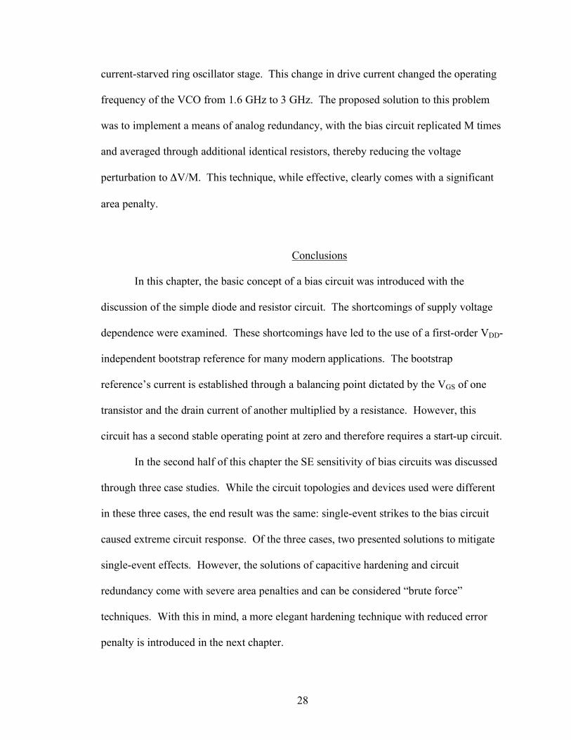
Fig. IV-8. The magnitude of the bias voltage point perturbation simulation results for
normal incidence and 60-degree angle strikes for all three circuits from the unperturbed
600 mV bias point. In both cases, the voltage excursion improves with SNACC. Note that
the improvement is greater in the angled-strike results. The SNACC device size
optimization made it much more favorable than a capacitor of equal area.
Fig. IV-9. Durations of voltage excursions exceeding 30 mV as a function of LET for
nominal and 60 degree angled strikes on the diode connected transistor shared with
transistor M4 compared with hardening of a capacitor of equal area and the unhardened
circuit. Again, the figures show an improvement in the SNACC results over the
unhardened and capacitor-hardened circuits with a greater improvement with angled
strikes. It is important to note that the smaller capacitor improves the duration
performance of capacitive hardening.

41
degree 40 MeV-cm2/mg strike to just one third of the unhardened circuit, and shaves
more than 400 ps off the duration.
One potential concern with the SNACC technique is that the area of sensitive
volume increases due to the additional devices, and therefore the probability of a strike
also increases. The responses of the introduced sensitive areas of the SNACC balancing
circuitry were simulated in the same way as the primary node. Note that, of the six added
transistors, only four are potentially vulnerable to SEs. A single-event strike to device
M1 or M7 will produce no noticeable perturbation to the bias point because those devices
are only active during a SE strike to the primary circuitry.
Simulations of strikes on the SNACC transistors showed that no single strike /
multi-node collection event combination to the added transistors caused a voltage
excursion larger than the maximum voltage excursions seen on the unhardened circuit for
a 40 MeV-cm2/mg 60 degree angled strike. These results are depicted in Fig. IV-10 for
perturbation amplitudes, and in Fig. IV-11 for durations of perturbations exceeding 30
mV. Consequently, the added vulnerable area does not significantly contribute to the
overall single-event vulnerability of the SNACC-hardened circuit.
Conclusions
The simulations in this work have shown that a reduction in single-event voltage
perturbation and transient duration at a critical node can be achieved in any standard
CMOS process through the use of balancing complementary circuitry combined with
careful layout techniques to encourage multi-node charge collection. The SNACC
technique is more area-efficient than the traditional capacitance hardening method, and
provides improved performance over the comparison circuits examined for both normal

42
and angled strikes. The greatest benefit of the SNACC technique was found to be in the
reduction of the effects of angled strikes, which have higher probability than strikes of
normal incidence. The greatest drawback to SNACC is that it introduces additional
sensitive area and raises the overall probability of a strike. However, strikes to this
additional sensitive area and the original diode connected transistor still show much
lower peak voltage excursions and time duration from the original bias circuit. This
point, coupled with the fact that this circuit technique will only become more effective as
devices scale further below 90 nm, makes it an attractive design option for RHBD
circuits.
Fig. IV-10. Perturbation amplitude analysis of the SNACC devices compared to the
unhardened circuit. On the left is normal incidence and the right 60 degree strikes for
LETs varying from 10-40 MeV-cm2/mg.

43
Fig. IV-11. Durations of perturbations exceeding 30 mV for the SNACC devices
compared to the unhardened circuit. On the left is normal incidence and the right is 60
degree strikes.
44
CHAPTER V
A RHBD BIAS CIRCUIT UTILIZING SNACC
Introduction
In the previous chapter, a new radiation-hardened-by-design (RHBD) technique
for analog circuits was presented. This technique, called sensitive node active charge
cancellation (SNACC), utilizes the phenomenon of multi-node charge collection to
reduce single-event voltage transients at sensitive nodes. SNACC was shown to be much
more effective than capacitive hardening when applied to a basic bias circuit consisting
of a diode-connected transistor and resistor. In this chapter, the SNACC technique will
be applied to a bootstrap current source circuit to demonstrate its effectiveness on a more
advanced bias circuit design.
Circuit Design
Fig. V-1(a) shows the bootstrap current source previously described in chapter III.
The circuit was designed using the IBM 90-nm process design kit (PDK) with 150 x 1
µm PMOS and 60 x 1 µm NMOS devices to provide a reference current of 26 µA. Fig.
V-2 shows a SE nodal analysis of this circuit using the bias-dependent model presented in
the previous chapter. Fig. V-2(a) shows the amplitude of the bias perturbation seen on a
mirrored/biased node, and Fig. V-2(b) shows the time that the node voltage was outside a
10% bias threshold for both normal incidence and 60 degree SE strikes. As Fig. V-2
shows, the node connecting the drains of device M2 and device M4 is by far the most
sensitive to SE strikes. In chapter IV, SNACC’s initial development focused primarily

45
on protecting a node with a single sensitive junction. However, the critical node in the
bootstrap circuit has two sensitive junctions, so SNACC must be extended to protect
them both.
Fig. V-1(b) shows a schematic of the SNACC-hardened bootstrap bias circuit
with the relative transistor sizes labeled. The main difference from the SNACC circuit
presented in chapter IV is that device M7 now is composed of two sets of parallel
devices. This modification extends the SNACC technique to protect both junctions at the
sensitive node. The additional circuitry in Fig. 1b does not change the overall DC
operation of the original circuit in any significant way. As previously shown, during
normal operation all the added devices are biased “off” and draw negligible additional
power.
Fig V-1. (a) Circuit diagram of the bootstrap current source. The startup circuitry is
highlighted gray and has minimal impact during normal circuit operation. (b) The
SNACC hardening technique applied to the node shared between M2 and M4 with the
relative W/L ratios labeled.

46
Fig. V-2. (a) SE perturbation amplitudes from a nodal analysis of circuit from fig. V-1
for normal incidence (left) and 60-degree (right) strikes. (b) SE perturbation durations
outside 10% of bias point for normal incidence (left) and 60-degree (right) strikes for
varying LET.
(a)
(b)

47
The successful implementation of the SNACC-hardened circuit requires that
transistors M12 and M7 are laid out as two sets of transistors in parallel. One set of
M12’s unit-cell transistors are interleaved with device M11 and the other set with device
M4, thus allowing maximum common charge collection of a SE strike on devices M11
and M12, or on devices M4 and M12. The two sets of interleaved PMOS devices are
placed in separate wells and separated by the NMOS devices to prevent multi-node
charge collection occurring between devices M11 and M4. NMOS devices M2 and M8
are interleaved in the same fashion with transistor M7.
A voltage transient can occur if transistor M4 sources (or M2 sinks) current from
a SE strike. If device M12 or M7 also collects charge, an equal current will ideally be
sourced or sunk through the current mirror of M8 and M9 (or M10 and M11), resulting in
no net change at the output node, thus mitigating the transient. The same mitigation
mechanism is present for PMOS devices M11 and M12, and also for NMOS devices M7
and M8. There is no impact on the circuit if a SE strike occurs on devices M10 or M9.
As previously discussed in chapter IV, the sizes of the SNACC current mirrors
M8-M9 and M10-M11 have an effect on the overall circuit’s area penalty as well as its
performance. The impact on performance is due to capacitive loading, and can be
replicated by placing an equivalent capacitor on the node instead. The size of these
devices can be optimized. Fig. V-3 shows the SE strike perturbation amplitudes and
durations following a 60-degree angled strike. Fig. V-3(a) shows strike amplitude and
duration versus the widths of M8 and M9 following a strike on M4. Fig. V-3(b) shows
strike amplitude and duration versus the widths of M10 and M11. Since L equals 1 !m,
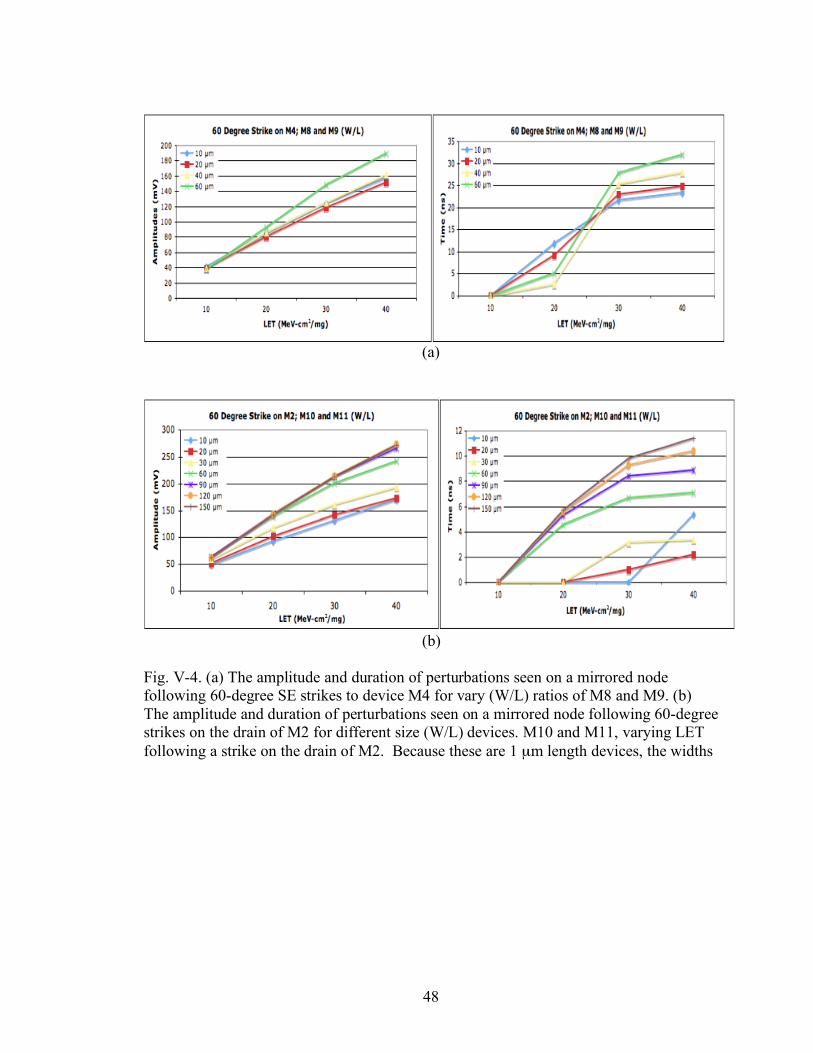
48
Fig. V-4. (a) The amplitude and duration of perturbations seen on a mirrored node
following 60-degree SE strikes to device M4 for vary (W/L) ratios of M8 and M9. (b)
The amplitude and duration of perturbations seen on a mirrored node following 60-degree
strikes on the drain of M2 for different size (W/L) devices. M10 and M11, varying LET
following a strike on the drain of M2. Because these are 1 µm length devices, the widths
(a)
(b)

49
the given widths are therefore equal to the (W/L) ratios.
In these simulations, the sizes of the SNACC devices were initially the same sizes
as the transistors in the baseline circuit and varied down to 10 x 1 µm devices. Overall
the 10 x 1 µm devices provided the best compromise between improved hardening and
reduced circuit area, and consequently 10 x 1 µm were used for the remainder of this
analysis.
Simulation Results
The circuits from Fig. V-1 (a and b) were simulated using the recently developed
transistor model [35] that captures the dynamic multi-node charge collection interactions
between devices, as discussed in chapter IV. Single-event strikes were simulated on
every transistor in the SNACC circuit by varying the strike’s linear energy transfer (LET)
from 10 to 40 MeV-cm2/mg in increments of 10 MeV-cm
2/mg, for both normal incidence
and 60 degree angled strikes.
Overall, five different circuits were simulated in this analysis. The first circuit
was the unhardened baseline circuit as depicted in Fig. V-1(a). The second circuit was
the baseline circuit hardened by adding a 413 fF capacitor to the critical node, where the
413 fF capacitor has an area equal to the SNACC devices. In the third circuit, devices
M3 and M4 were interleaved in the baseline circuit. The third circuit was then hardened
with a 413 fF capacitor to create the fourth circuit. The fifth circuit was the SNACC-
hardened circuit of Fig. V-1(b). Note that circuits three and four were simulated to
determine if interleaving M3 and M4 provided any intrinsic hardening benefit even if
SNACC was not used.

50
The response of these five circuits to SE strikes was measured for both
perturbation amplitude and durations exceeding a 10% threshold of the bias point. Fig.
V-4 shows the results for strikes to M4, (a) for amplitude and (b) duration. It is
interesting to note that interleaving M4 and M3 provides a significant increase to overall
hardness following strikes to the drain of M4. However, this improvement occurs
because the M3 drain node is a relatively insensitive node as seen from Fig. V-2(a). A
designer would want to avoid this interleaved M3-M4 layout because it also subjects
device M3 to the SE “softness” of device M4, therefore degrading the circuit’s overall
single-event response.
Fig. V-4 clearly shows the merit of the SNACC approach for hardening the drain
junction of device M4 in the bootstrap bias circuit. SNACC improves the circuit’s SE
immunity for normal incidence and 60-degree strikes for both perturbation amplitude and
duration. For a 60-degree angled strike with LET of 40 MeV-cm2/mg, SNACC reduces
the perturbation amplitude and durations to less than one-third of capacitive hardening
alone.
SNACC was quite successful at hardening the sensitive drain junction of device
M4 on the critical node, but still had to be evaluated for strikes to the drain of device M2.
This case was simulated in the same manner as before with the same five circuits, except
that M2 and M1 were interleaved in circuits three and four, rather than transistors M3 and
M4. These circuits were evaluated for both perturbation amplitude and duration
exceeding a 10% bias threshold for varying LET at normal incidence and 60 degrees.
The results are shown in Fig. V-5 (a) and (b).
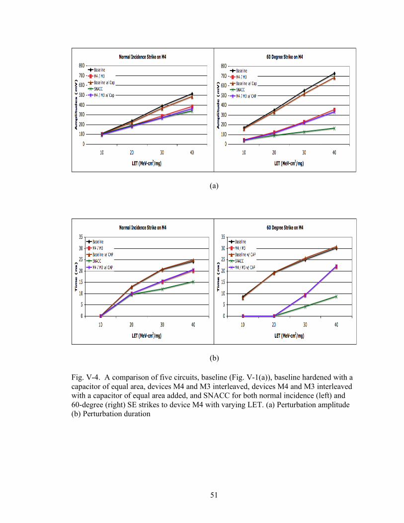
51
Fig. V-4. A comparison of five circuits, baseline (Fig. V-1(a)), baseline hardened with a
capacitor of equal area, devices M4 and M3 interleaved, devices M4 and M3 interleaved
with a capacitor of equal area added, and SNACC for both normal incidence (left) and
60-degree (right) SE strikes to device M4 with varying LET. (a) Perturbation amplitude
(b) Perturbation duration
(a)
(b)

52
The results in Fig. V-5 show that interleaving M2 with M1 provides significant
hardness to the overall circuit after a strike to the drain of M2. However, as with the M3-
M4 interleaving, a designer would avoid such a layout because of the effect of strikes on
the drain of M1. In fact, interleaving these devices causes a 56% increase in perturbation
amplitude following strikes to M1 alone for angled 40 MeV-cm2/mg strikes. Overall,
SNACC provides a significant hardening advantage over other methods, and reduces 60-
degree 40 MeV-cm2/mg strike perturbations to roughly one-third of capacitive hardening
alone.
The overall effectiveness of SNACC is still somewhat difficult to picture, because
of the separate analysis of strikes to the drains of M4 and M2. A relatively simple way to
get a “single shot” comparison of the effectiveness of SNACC is to examine the nodal
analysis from Fig. V-2 with and without SNACC applied. In Fig. V-2, the most sensitive
node containing the drains of M4 and M2 were represented in red and black respectively.
Fig. V-6 shows the same analysis for 60-degree angled strikes with the original values for
M4 and M2 in gray for reference. The values of M4 and M2 with SNACC applied are
now represented in red and black, respectively. Notice the difference in the sensitivity of
those nodes. The M3 drain node, not the node connecting M4 and M2, is now the most
sensitive node. The addition of SNACC has reduced the peak perturbation amplitude for
a 60-degree 40 MeV-cm2/mg strike by approximately 400 mV, and reduced the duration
by approximately 16 ns.

53
Fig. V-5. A comparison of five circuits, baseline (Fig. V-1(a)), baseline hardened with a
capacitor of equal area, devices M2 and M1 interleaved, devices M2 and M1 interleaved
with a capacitor of equal area, and SNACC for both normal incidence (left) and 60-
degree (right) SE strikes to device M2 with varying LET. (a) Perturbation amplitude (b)
Perturbation duration
(a)
(b)
54
Circuit Design with SNACC
Up to this point, the focus of this work has been on demonstrating a new
hardening technique for bias circuits, and applying that technique to a useful bias circuit
design, respectively. This section will focus on optimizing the bootstrap design and then
working through an example from start to finish on the implemention of a hardened
current source utilizing SNACC. The circuit topology for this section will remain the
same as before, with a designed bias current of 26 µA.
As previously discussed in chapter III, designers typically spend much time and
effort in developing a high-quality current source. The output of that single current
source is then typically mirrored off to other subcircuits in the IC. There are many
factors that go into a precision analog design , but matching usually plays a very large
role.
In analog design, long channel devices are commonly used to mitigate the effects
of channel length modulation and improve matching. Consequently, 1 µm length
MOSFETs were chosen for just that reason in the previous chapters. However, achieving
good matching is certainly possible with shorter device channel lengths. In Fig. V-7, the
percent mismatch of the drain current of devices M3 and M4 from Fig. V-1 is plotted as a
function of channel length. Almost negligible mismatch is observed for a 0.5 µm channel
length. In order to construct a precision current source possible with the minimum area,
the bootstrap current source was redesigned with all transistors at L = 0.5 !m.

55
Fig. V-6. A nodal analysis of the bootstrap bias circuit. Shown in gray are the values for
perturbation amplitude (left) and duration (right) following 60-degree strikes for varying
LET. These are the same values from Fig. V-2. Those gray lines are now represented in
the same colors as Fig. V-2 with SNACC applied. The M3 drain is now the most
sensitive junction, with a reduction of approximately 400 mV and 16 ns at an LET of 40
MeV-cm2/mg compared to the unhardened circuit.
Fig. V-7. Percent mismatch of current (y-axis) between devices M3 and M4 in the
bootstrap design as a function of channel length (x-axis). The circuit has almost no
degradation in matching down to 0.5 µm channel length.

56
After redesigning the circuit, the next step in the design process was to analyze
the SE response of the circuit, node by node. Fig. V-8 shows the amplitude (a) and the
duration (b) of the perturbations per node as a function of LET for 60-degree strikes. As
expected, the node shared between the drains of device M4 and M2 was still the most
sensitive. It is interesting to note that at the smaller channel lengths the sensitivity of
drain M4 dominates, and the M2 drain remains the next most sensitive junction, but is
closer to the average sensitivity of the other junctions.
The next step in the design process was to apply SNACC to the sensitive junction
and optimize it for device size. Changing the channel length of the devices did not
change the most sensitive junction, so the SNACC-hardened circuit has the same
topology as the circuit in Fig. V-1 (b). In order to optimize the SNACC design, strikes
to M4 were simulated for different W/L values for devices M8 and M9. Strikes to M2
were also simulated for different W/L values for devices M10 and M11. The intent was
to maximize performance (SE mitigation) and minimize area penalty (device size).
In Fig. V-9 the results of this analysis are depicted for 60-degree strikes on M4.
On the left are shown the perturbation amplitudes and on the right are shown the
durations exceeding a 10% bias threshold. It is interesting to note that reducing the
device size had little effect on amplitude following strikes to M4, but the smaller devices
tended to make a difference in duration mitigations, particularly at higher LETs. The best
compromise between improved performance and reduced area penalty occurred with the
choice of 5 x 0.5 µm devices (i.e. W/L ratio = 10).

57
(a)
(b)
Fig. V-8. Nodal analysis of the bootstrap current source with .5 µm channel lengths
depicting the perturbation amplitudes (a) and durations exceeding a 10% bias threshold
(b) as a function of LET.

58
In Fig. V-10, the results of a similar analysis are shown for 60-degree strikes to
M2. Again, on the left are shown are the perturbation amplitudes and on the right are
shown are the durations exceeding a 10% bias threshold for varying LET and device size
(W/L ratio). The choice here is clearer that for the previous case. The 5 x 0.5 µm
devices (W/L ratio = 10) provide the best performance and least area penalty. The
overall layout of this circuit with the optimized device sizes is depicted in Fig. V-11.
Once the entire SNACC-hardened circuit design was completed, the next stage
was to analyze the results. The bias-dependent model previously described was used to
simulate normal incidence and 60-degree angled strikes to every node in the circuit for
LETs ranging from 10 to 40 Mev-cm2/mg. Three circuits were compared in this analysis;
the unhardened baseline circuit, the baseline circuit hardened by a 6-level metal 136 fF
capacitor equal in area to the SNACC circuitry, and the SNACC-hardened bias circuit.
Fig, V-12 shows a sample waveform, typical of the response seen throughout this section,
which compares the response of the three circuits following a 40 MeV-cm2/mg strike to
device M2.
In Fig. V-13, the results for perturbation amplitude for normal incidence (left) and
60-degree strike (right) are shown following strikes to M4. SNACC provides an even
more dramatic reduction in perturbation amplitudes for the smaller device lengths.
SNACC reduces the perturbation amplitude of a 60-degree angled strike with a LET of
40 MeV-cm2/mg to just one-third that of capacitive hardening alone.
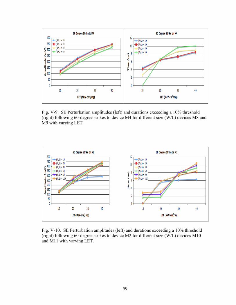
59
Fig. V-9. SE Perturbation amplitudes (left) and durations exceeding a 10% threshold
(right) following 60-degree strikes to device M4 for different size (W/L) devices M8 and
M9 with varying LET.
Fig. V-10. SE Perturbation amplitudes (left) and durations exceeding a 10% threshold
(right) following 60-degree strikes to device M2 for different size (W/L) devices M10
and M11 with varying LET.

60
Fig. V-11. Fig. V-3. Layout view of SNACC applied to the bootstrap current source. The
SNACC devices are shown in red (PMOS) and yellow (NMOS), while the current source
devices are blue (PMOS) and gray (NMOS)
Fig. V-12. Waveform for a 40 MeV-cm
2/mg strike to M2. The three circuits depicted
are the baseline (brown), baseline hardened with a capacitor (red), and the baseline
hardened by SNACC (blue).

61
Fig. V-13. Perturbation amplitudes following normal incidence (left) and 60-degree
angled (right) SE strike to device M4. There are three circuits being compared the
baseline, the baseline hardened with a capacitor of equal area to the SNACC circuit, and
the SNACC circuit for varying LET.
Fig. V-14. Perturbation durations exceeding a 10% bias threshold following normal
incidence (left) and 60-degree angled (right) SE strike to device M4. There are three
circuits being compared the baseline, the baseline hardened with a capacitor of equal area
to the SNACC circuit, and the SNACC circuit for varying LET.

62
As previously observed, SNACC clearly outperforms capacitive hardening for
perturbation amplitude mitigation. Previous work also showed that SNACC reduced
perturbation durations compared to capacitive hardening. This result is confirmed in Fig.
V-14. SNACC reduces the perturbation duration of a 40 MeV-cm2/mg 60-degree strike
to M4 to just a little over one-third of capacitive hardening. These results are promising
because the nodal analysis of Fig. V-8 shown that the response of M4 to SE strikes was
by far the worst case.
SNACC clearly improved the SE response of the drain of M4, the most sensitive
junction on the critical node. The next step in the analysis was to evaluate the response
of the drain of M2, other vulnerable node junction. Fig. V-15 shows the perturbation
amplitudes following normal incidence (left) and 60-degree angled (right) strikes to
device M2. In this case, SNACC does not provide as much benefit for normal incidence
strikes (which are much less common than angled strikes), but does provide a significant
improvement in amplitude reduction for 60 degree strikes. As previously discussed, the
charge sharing improves for angled strikes, and therefore the SNACC concept works
even better in such cases. SNACC reduced the perturbation amplitude following a 60-
degree 40 MeV-cm2/mg strike to M2 to almost half of just capacitive hardening alone.
Fig. V-16 shows the perturbation duration data following strikes of normal
incidence (left) and 60-degree incidence (right) to the drain of M2. While not as dramatic
as the results for M4, they are still quite convincing. SNACC reduced the perturbation
duration following a 60-degree 40 MeV-cm2/mg strike to approximately two-thirds of
capacitive hardening alone.

63
Fig. V-15. Perturbation amplitudes following normal incidence (left) and 60-degree
angled (right) SE strike to device M2. There are three circuits being compared the
baseline, the baseline hardened with a capacitor of equal area to the SNACC circuit, and
the SNACC circuit for varying LET.
Fig. V-16. Perturbation durations exceeding a 10% bias threshold following normal
incidence (left) and 60-degree angled (right) SE strike to device M2. There are three
circuits being compared the baseline, the baseline hardened with a capacitor of equal area
to the SNACC circuit, and the SNACC circuit for varying LET.

64
The final step in the analysis was to compare the original nodal analysis from Fig.
V-8 to the hardened circuit with SNACC applied. The drain junctions of M4 and M2
without SNACC are shaded gray for comparison, and the junctions with SNACC applied
are shown in red and purple respectively. This analysis is depicted in Fig. V-17. The
perturbation amplitude of the most sensitive junction dropped roughly 740 mV for 60-
degree strikes with an LET of 40 MeV-cm2/mg. Furthermore, the most sensitive junction
is now the source of M2, rather than the node connecting the M2 and M4 drains. The
duration data is equally convincing, showing that the strike duration at the most sensitive
junction for the same case was reduced approximately 11 ns.
Conclusions
These simulations have shown that the use of SNACC can dramatically reduce the
effects of a SE on a critical analog node in terms of amplitude and duration. The SNACC
technique was applied to the same bias circuit with two different channel lengths and
provided favorable results for both. The performance of SNACC improved for the
smaller channel lengths over capacitive hardening, partly because the capacitance that
could be achieved with equal area to the SNACC circuitry was also reduced. Finally, a
nodal analysis with and without SNACC showed the amplitude and duration of
perturbations to the most sensitive junctions following a 60-degree 40 MeV-cm2/mg
strike could be reduced by 740 mV and 11 ns, respectively.

65
Fig. V-17. A nodal analysis of the bootstrap circuit with SNACC applied. On the left are
perturbation amplitudes and on the right the durations for 60-degree strikes. The original
values for the drains of M4 and M2 are left in gray for comparison.

66
CHAPTER VI
CONCLUSIONS
The sensitivity of many bias circuits to single-event effects combined with the
difficulty of applying standard RHBD techniques to analog and mixed-signal circuits has
led to the development of SNACC, a novel hardening technique that can be applied to
any sensitive/critical circuit node. This technique was initially developed and applied to
a simple bias circuit with just a single vulnerable junction.
The drawbacks of this basic single node circuit as a bias circuit were explored
with emphasis on supply voltage dependence. A bootstrap current source was introduced
as a better option. Through derivation of its equilibrium equations, its first-order supply
voltage independence was illustrated. The common issue of multiple stable operating
points in bootstrap current sources was discussed and solved via a start-up circuit. The
SE nodal analysis of this circuit revealed that the critical node of the circuit had two
vulnerable junctions. Consequently, the SNACC circuit’s symmetry was modified to
protect multiple junctions at the same node. The circuit was simulated and the results
showed that the most sensitive junction could be reduced by 400 mV and 16 ns for
perturbation amplitude and duration respectively at a 60-degree 40 MeV-cm2/mg strike.
The effects of channel length modulation were explored to determine optimal
device sizing. Simulations showed that a high precision of matching could be maintained
down to a 0.5 µm channel length. The bootstrap circuit was optimized with this channel
length, providing a step-by-step process for a designer to follow. The circuit was
simulated again for perturbation amplitudes and durations. A nodal analysis of the

67
hardened circuit showed that not only was it much more effective than capacitive
hardening, but SNACC could reduce perturbation amplitudes and durations for a 60-
degree 40 MeV-cm2/mg strike by 740 mV and 11 ns respectively.
The SNACC technique has two potential drawbacks of note: increased layout
complexity and increased number of vulnerable junctions. The layout complexity is not a
significant concern, as interleaving of devices to promote matching is already a common
practice in analog and mixed-signal design. Furthermore, simulations show that the
additional junctions introduced by SNACC tend to be self-compensating, and are much
less sensitive then the junctions of the original unhardened circuit. Through optimization
and careful design, SEE perturbation amplitudes and durations can be reduced to just
25% those of an unhardened circuit in certain cases.
These results show that SNACC can be a very effective tool for analog and
mixed-signal RHBD applications, and should remain so as device sizes are scaled to
smaller dimensions. Future research will focus on hardware verification of this
technique, and its extension to other precision analog and mixed-signal subcircuits.

68
REFERENCES
[1] K. Kruckmeyer, R. L. Rennie, and V. Ramachandran, “Use of Code Error and
Beat Frequency Test Method to Identify Single Event Upset Sensitive Circuits in
a 1 GHz Analog to Digital Converter”, IEEE Trans. Nucl. Sci., pp. 1-5, Dec.
2007.
[2] Y. Boulghassoul, S. Buchner, D. McMorrow, V. Pouget, L. W. Massengill, P.
Fouillat, W. T. Holman, C. Poivey, J. W. Howard, M. Savage, and M. C. Maher,
“Investigation of Millisecond-Log Analog Single-Event Transients in the
LM6144 Op Amp”, IEEE Trans. Nucl. Sci., vol. 51, no 6, pp 3529-3536, Dec.
2004.
[3] T. D. Loveless, L. W. Massengill, W. T. Holman, and B. L. Bhuva, “Modeling
and Mitigating Single-Events Transients in Voltage-Controlled Oscillators” IEEE
Trans. Nucl. Sci., vol. 54, no. 6, pp. 2561-2567, Dec. 2007.
[4] L. W. Massengill, O. A. Amusan, S. Dasgupta, A. L. Sternberg, J. D. Black, A. F.
Witulski, B. L. Bhuva, M. L. Alles, “Soft-Error Charge-Sharing Mechanisms at
Sub-100nm Technology Nodes” IEEE Conference on Integrated Circuit Design
and Technology ICICDT, pp. 1-4, 2007.
[5] H. C. Koons, J. E. Mazur, R. S. Selesnick, J. B. Blake, J. F. Fennell, J. L. Roeder,
and P. C. Anderson, “The Impact of the Space Environment on Space Systems,”
Aerospace Technical Report, no. TR-99(1670)-1, July, 1999.
[6] J. Mazur, “The Radiation Environment Outside and Inside a Spacecraft,” in IEEE
NSREC Short Course, 2002, pp. II-1 – II-69.
[7] J. R. Srour, C. J. Marshall, and P. W. Marshall, “Review of Displacement
Damage Effects in Silicon Devices,” IEEE Trans. Nucl. Sci., vol. 50, no. 3, pp.
653-670, June 2003.
[8] D. R. Alexander, “Transient Ionizing Radiation Effects in Devices and Circuits,”
IEEE Trans. Nucl. Sci., vol. 50, no. 3, pp. 565-582, June 2003.
[9] T. R. Oldham and F. B. McLean, “Total Ionizing Dose Effects in MOS Oxides
and Devices,” IEEE Trans. Nucl. Sci., vol. 50, no. 3, pp. 483-499, June 2003.
[10] P. Meyer, R. Ramaty, and W. R. Webber, “Cosmic Rays: Astronomy with
energetic particles,” Physics Today 27, 1974

69
[11] J. F. Ziegler, H. W. Curtis, H. P. Muhlfeld, C. J. Montrose, B. Chin, M. Nicewicz,
C. A. Russell, W. Y. Wang, L. B. Freeman, P. Hosier, L. E. LaFave, J. L. Walsh,
J. M. Orro, G. J. Unger, J. M. Ross, T. J. O’Gorman, B. Messina, T. D. Sullivan,
A. J. Sykes, H. Yourke, T. A. Enger, V. Tolat, T. S. Scott, A. H. Taber, R. J.
Sussman, W. A. Klein, and C. W. Wahaus, “IBM Experiments in Soft Fails in
Computer Electronics (1978-1994),” IBM J. Res. Develop., vol. 40, no. 1, 1998.
[12] G. Holman and S. Benedict, “Solar Flare Theory Educational Web Pages,”
Heliophysics Science Division, NASA/Goddard Space Flight Center, Solar
Physics Laboratory, [Online]. Available:
http://hesperia.gsfc.nasa.gov/sftheory/flare.htm, Aug. 2007.
[13] National Aeronautics and Space Administration’s Goddard Space Flight Center,
Solar & Heliospheric Observatory (SOHO) Project. [Online]. Available:
http://visibleearth.nasa.gov/view_rec.php?id=1675.
[14] E. G. Stassinopoulos and J. P. Raymond, “The Space Radiation Environment for
Electronics,” Proc. Of the IEEE, vol. 76, pp. 1423-1442, Nov. 1988.
[15] J. A. Van Allen, C. E. McIlwain, and G. H. Ludwig, “Radiation Observations
with Satellite 1958 EX,” J. Geophys. Res., vol. 64, no. 3, pp. 271-286, 1959.
[16] J. L. Barth, C. S. Dyer, and E. G. Stassinopoulos, “Space, Atmospheric, and
Terrestrial Radiation Environments,” IEEE Trans. Nucl. Sci., vol. 50, no. 3, pp.
466-482, June 2003.
[17] E. Petersen, “Soft Errors Due to Protons in the Radiation Belt,” IEEE Trans. Nucl.
Sci., vol. 28, pp. 3981-3986, Dec. 1981.
[18] F. Wrobel, J. M. Palau, M. C. Calvet, O. Bersillon, and H. Duarte, “Incidence of
Multi-Particle Events on Soft Error Rates Caused by n-Si Nuclear Reactions,”
IEEE Trans. Nucl. Sci., vol. 47, pp. 2580-2585, Dec. 2000.
[19] P. E. Dodd, “Basic Mechanisms for Single-Event Effects,” in IEEE NSREC Short
Course, 1999, pp. II-1 – II-85.
[20] L. W. Massengill, “SEU Modeling and Prediction Techniques,” in IEEE NSREC
Short Course, 1993, pp. III-1 – III-93.
[21] C. M. Hsieh, P. C. Murley, and R. R. O’Brien, “A Field-Funneling Effect on the
Collection of Alpha-Particle-Generated Carriers in Silicon Devices,” IEEE
Electron Device Letters, vol. 2, no. 4, pp. 103-105, Apr. 1981.

70
[22] S. DasGupta, A. F. Witulski, B. L. Bhuva, M. L. Alles, R. A. Reed, O. A.
Amusan, J. R. Ahlbin, R. D. Schrimpf, and L. W. Massengill, “Effects of Well
and Substrate Potential Modulation on Single Event Pulse Shape in Deep
Submicron CMOS,” IEEE Trans. Nucl. Sci., vol. 54, no. 6, pp. 2407-2412, Dec.
2007.
[23] S. DasGupta, “Trends in Single Event Pulse Widths and Pulse Shapes in Deep-
Submicron CMOS,” M.S. Thesis, Dec. 2007.
[24] R. S. Muller, T. I. Kamins, and M. Chan, “Device Electronics for Integrated
Circuits,” Third Ed. John Wiley & Sons, Inc., 2003.
[25] R. Baumann, “Single-Event Effects in Advanced CMOS,” in IEEE NSREC Short
Course, 2005, pp. II-1 – II-59.
[26] A. D. Tipton, J. A. Pellish, R. A. Reed, R. D. Schrimpf, R. A. Weller, M. H.
Mendenhall, B. Sierawski, A. K. Sutton, R. M. Diestelhorst, G. Espinel, J. D.
Cressler, P. W. Marshall, and G. Vizkelethy, “Multi-Bit Upset in 130 nm CMOS
Technology,” IEEE Trans. Nucl. Sci., vol. 53, no. 6, pp. 3259-3264.
[27] K. F. Galloway and G. H. Johnson, “Catastrophic Single Event Effects in the
Natural Environment,” in IEEE NSREC Short Course, 1996, pp. IV-1 – IV-72.
[28] A. H. Johnston, “The Influence of VLSI Technology evolution on Radiation-
Induced Latchup in Space Systems,” IEEE Trans. Nucl. Sci., vol. 43, n. 2, pp.
505-521, Apr. 1996.
[29] A. W. Waskiewicz, J. W. Groniger, V. H. Strahan, and D. M. Long, “Burnout of
Power MOS Transistors with Heavy Ins of Californium-252,” IEEE Trans. Nucl.
Sci., vol. 33, no. 6, pp. 1710-1713, Dec. 1986.
[30] P. E. Allen and D. R. Holberg, “CMOS Analog Circuit Design,” Second Ed.
Oxford university Press, 2002.
[31] O. A. Amusan, L. W. Massengill, M. P. Baze, A. L. Sternberg, A. F. Witulski, B.
L. Bhuva, and J. D. Black, “Single Event Upsets in Deep-Submicrometer
Technologies Due to Charge Sharing” IEEE Trans. Nucl. Sci. vol. 8 no. 3, pp.
582-589, Dec. 2008.
[32] O. A. Amusan, A. F. Witulski, L. W. Massengill, B. L. Bhuva, P. R. Fleming, M.
L. Alles, A. L. Sternberg, J. D. Black, and R. D. Shrimpf, “Charge Collection and
Charge Sharing in a 130 nm CMOS Technology” IEEE Trans. Nucl. Sci. vol. 53
no.6, pp. 3253-3258, Dec. 2006.

71
[33] A. T. Kelly, P. R. Fleming, W. T. Holman, A. F. Witulski, B. L. Bhuva, and L. W.
Massengill, “Differential Analog Layout for Improved ASET Tolerance” IEEE
Trans. Nucl. Sci. vol. 54 no. 6, pp. 2053-2059, Dec. 2007.
[34] S. E. Armstrong, et al, “Demonstration of a Differential Layout Solution for
Improved ASET Tolerance in CMOS A/MS Circuits,”
Accepted for presentation
at the 2010 Nuclear and Space Radiation Effects Conference, Denver, Co, July,
2010
[35] Jeffrey S. Kauppila, A. L. Sternberg, M. L. Alles, A. M. Francis, J. Holmes, O. A.
Amusan, and L. W. Massengill, “A Bias-Dependent Single-Event Compact
Model Implemented Into BSIM4 and a 90 nm CMOS Process Design Kit” IEEE
Trans. Nucl. Sci. vol. 56 no. 6, pp. 3152-3157, Dec. 2009.
[36] O. A Amusan, L. W. Massengill, M. P. Baze, B. L. Bhuva, A. F. Witulski, S.
DasGupta, A. L. Sternberg, P. R. Fleming, C. C. Heath, M. L. Alles, “Directional
Sensitivity of Single Event Upsets in 90 nm CMOS Due to Charge Sharing” IEEE
Trans. Nucl. Sci. vol 54 no. 6, pp. 2584-2589, Dec. 2007.
Related Documents