The Design of Asynchronous Memory Management Unit Chris Myers Alain Martin Computer System Lab. CS Dept. Stanford University Cal. Tech

The Design of Asynchronous Memory Management Unit Chris Myers Alain Martin Computer System Lab. CS Dept. Stanford University Cal. Tech.
Dec 17, 2015
Welcome message from author
This document is posted to help you gain knowledge. Please leave a comment to let me know what you think about it! Share it to your friends and learn new things together.
Transcript

The Design of Asynchronous Memory Management Unit
Chris Myers Alain Martin Computer System Lab. CS Dept. Stanford University Cal. Tech

Asynchronous Memory Management Unit• What is a MMU? 16 bit virtual address ==> a 24 bit physical address. ma (memory address) ra (real address)

Memory Management Unit
16 bit virtual address + 8-bit segmentation register ==> a 24 bit physical address. sr: Segementation Read register (FFFF) sw: Segementation Write register (FFFE)
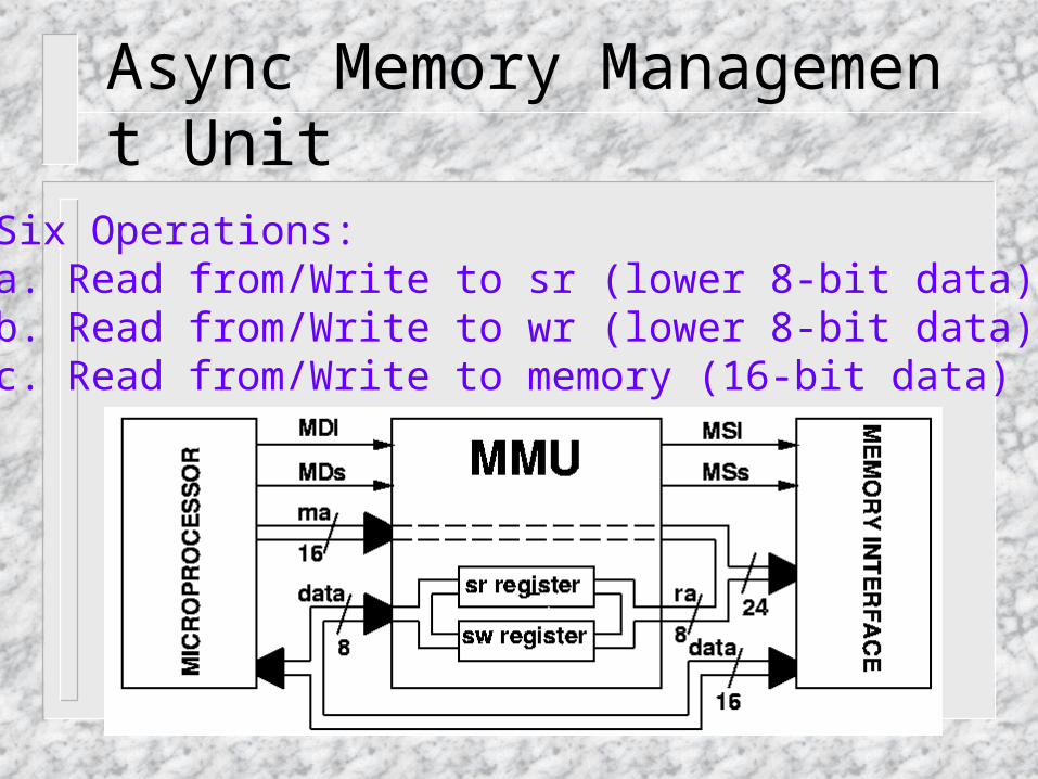
Async Memory Management Unit• Six Operations: a. Read from/Write to sr (lower 8-bit data) b. Read from/Write to wr (lower 8-bit data) c. Read from/Write to memory (16-bit data)

Async Memory Management Unit
• 4 control signals: a. MDl: memory data load (mem or Seg Reg==>CPU) b. MDs: memory data store (CPU==>mem or Seg Reg) c. MSl: memory storage load. d. MSs: memory storage store.

Memory Load
• Wait for communication on MDl port • Do memory address comparison ma=FFFEh (load from wr) ma=FFFFh (load from sr) otherwise load from memory.• Put sr on real address bus (ra=sr) • Request memory load from Memory Interface (initiate a communication on MSl)• Wait until load is acknowledged then complete communication on MDl port

Store Seg. Read Register
• Wait for communication on MDs port • Do memory address comparison check ma=FFFFh • Put value from data bus into the sr register • Complete communication on MDs port

Design Flow
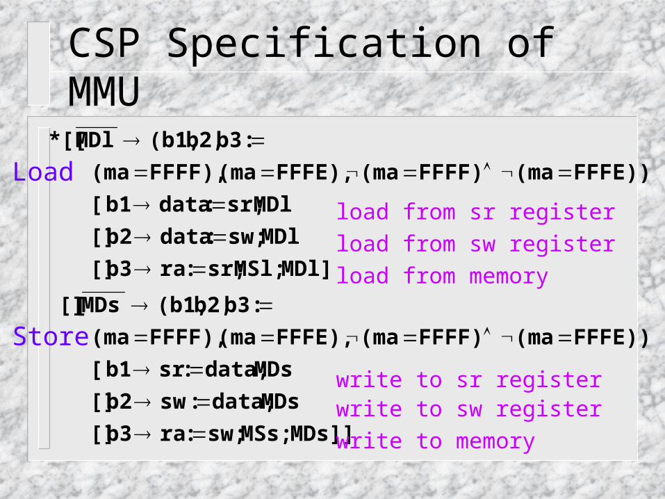
CSP Specification of MMU
MDs]]MSs;sw;:rab3 []
MDsdata;:swb2 []
MDsdata;:srb1 [
FFFE));(maFFFF)(maFFFE),(maFFFF),(ma
:b3b2,(b1,MDs[ []
MDl]MSl;sr;:rab3 []
MDlsw;:datab2 []
MDlsr;:datab1 [
FFFE));(maFFFF)(maFFFE),(maFFFF),(ma
:b3b2,(b1,MDl[[*
Load
Store
load from sr register
load from sw register
load from memory
write to sr registerwrite to sw register
write to memory

Optimizing CSP Specification
• Logic:
• Time:ma0b3b2
ma0b3b1
FFFE)(maFFFF)(mab3
FFFE)(maFFFF)(mab3
)τMax(ττ
)τMax(ττ
ττ
τττ
rama,reg
rama,mem
mareg
ramamem

Optimizing CSP Specification
MDs]]MSs;b3 []
MDsdata;:swb2 []
MDsdata;:srb1 [
ma0));b3ma0,b3b2b1,
FFFE);(maFFFF)(ma:(b3||sw):((raMDs[ []
MDl]MSl;b3 []
MDlsw;:datab2 []
MDlsr;:datab1 [
ma0));b3ma0,b3b2b1,
FFFE);(maFFFF)(ma:(b3||sr):((raMDl[[*

Process Decomposition
• Control path:

Process Decomposition
• Datapath: A. comparator:
B. Registers:

Memory Data Load Cycle

Handshaking Expansion

Handshaking Expansion

Handshaking Expansion

Handshaking Expansion

Handshaking Expansion
• Reshuffling

Production Rule Expansion
• Load data from sr register:
Guard Strengthening: Make the order of transitions confirmwith CSP specification.

PR Implementation

Handshaking Expansion:datapath
• Datapath:
• Reshuffling:
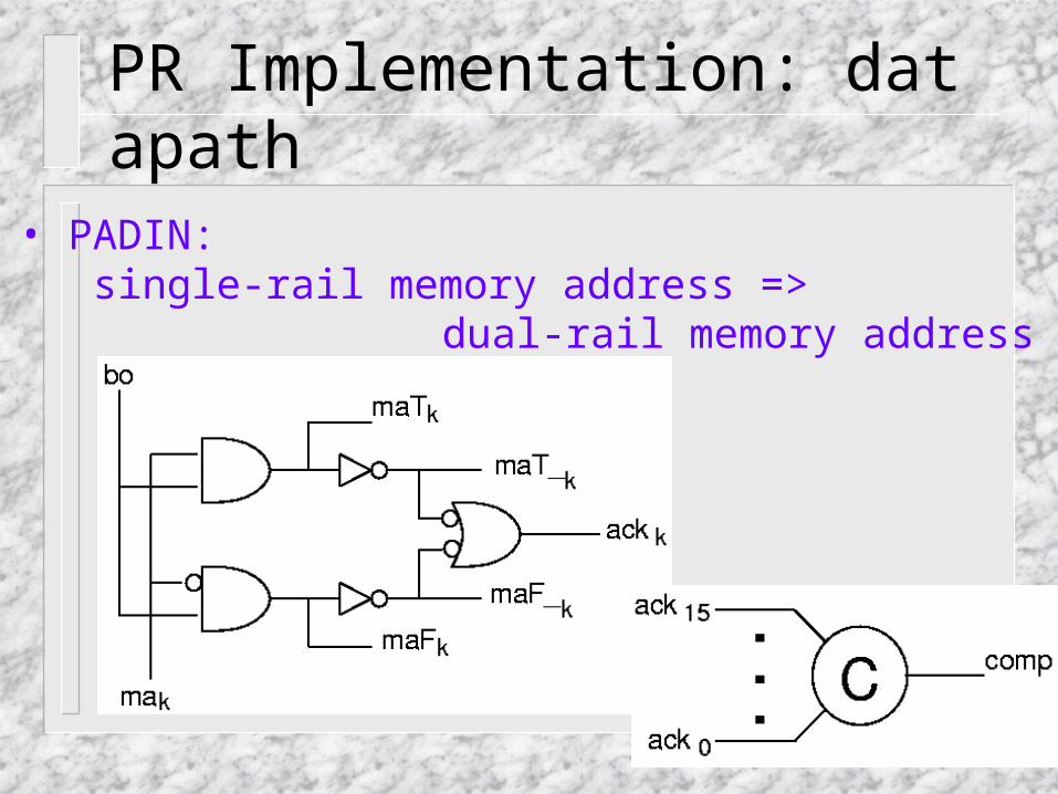
PR Implementation: datapath
• PADIN: single-rail memory address =>
dual-rail memory address

PR Implementation: datapath
• determines if bits ma15-ma1 are all high.

PR Implementation: datapath
• determines if bits ma15-ma1 are all high.
Related Documents