Research Article Chaochao Jian, Xiangchao Ma*, Jianqi Zhang and Jiali Jiang The anisotropic broadband surface plasmon polariton and hot carrier properties of borophene monolayer https://doi.org/10.1515/nanoph-2021-0599 Received October 18, 2021; accepted December 24, 2021; published online January 11, 2022 Abstract: Borophene monolayer with its intrinsic metallic and anisotropic band structures exhibits extraordinary electronic, optical, and transport properties. Especially, the high density of Dirac electrons enables promising applications for building low-loss broadband SPP devices. However, a systematic characterization of the surface plasmon polariton (SPP) properties and hot carriers generated from the inevitable SPP decay in borophene has not been reported so far. Most importantly, the mechanism for SPP losses remains obscurely quantified. In this work, from a fully first-principles perspective, we explicitly evaluate the main loss effects of SPP in borophene, including the Drude resistance, phonon-assisted intraband and direct interband electronic transitions. With this knowledge, we further calculate the frequency- and polarization-dependent SPP response of borophene, and evaluate some typical application-dependent figure of merits of SPP. On the other hand, we evaluate the gener- ation and transport properties of plasmon-driven hot car- riers in borophene, involving energy- and momentum- dependent carrier lifetimes and mean free paths, which provide deeper insight toward the transport of hot carriers at the nanoscale. These results indicate that borophene has promising applications in next-generation low-loss opto- electronic devices and photocatalytic reactors. Keywords: borophene monolayer; first-principles; hot carriers; surface plasmon polariton. 1 Introduction Surface plasmon polariton (SPP) [1] is the collective oscil- lation of free electrons at metal/dielectric interfaces induced by incident light with a specific frequency, which has been attracting great attention in the realm of nano- photonics and optoelectronics. In these systems, the elec- tromagnetic field of SPP is evanescently confined in the normal direction of the interface, thus breaking the optical diffraction limit [2]. These unique properties enable the miniaturization of optoelectronic devices and nanoscale regulation of light field, and therefore have broad appli- cations, such as integrated nanophotonics [3], photo- catalysis [4], and sensing detection [5]. Practically, it is required that SPP exhibits low damp- ing and wide visible plasmonic response, which is one of the current research hotspots in exploring the SPP prop- erties of new materials [6, 7]. In the limit of extreme quantum confinement and low dimensionality, excellent SPP is expected to appear in emerging new materials. For example, Nao Zhang et al. indicated that the SPP propa- gation length of Ag nanowire is prominently increased to about 7 μm [8]. Meanwhile, two-dimensional (2D) materials are widely studied, especially the well-known graphene [9] and noble metal films (Au and Ag) [10]. However, the fre- quencies of plasmonic response in these materials are mostly limited to the infrared region, where the develop- ment of optoelectronic detectors or light sources is rela- tively slow compared with the visible light range. Although the frequencies of plasmonic response can usually be extended into the visible region by increasing the carrier concentration, it also adversely results in high loss due to the increase of phase space for electron–phonon scat- tering. Therefore, it is urgent to find a plasmonic material with low losses and broadband response for further development applications in optoelectronics, nano- photonics, and photocatalysis. Recently, some theoretical studies have predicted that borophene, a single atomic-layer of boron, shows unique electronic, optical, and transport properties, which is *Corresponding author: Xiangchao Ma, School of Physics and Optoelectronic Engineering, Xidian University, Xi’an 710071, China, E-mail: [email protected]. https://orcid.org/0000-0002-0579- 0190 Chaochao Jian, Jianqi Zhang and Jiali Jiang, School of Physics and Optoelectronic Engineering, Xidian University, Xi’an 710071, China, E-mail: [email protected] (C. Jian), [email protected] (J. Zhang), [email protected] (J. Jiang) Nanophotonics 2022; 11(3): 531–541 Open Access. © 2022 Chaochao Jian et al., published by De Gruyter. This work is licensed under the Creative Commons Attribution 4.0 International License.

Welcome message from author
This document is posted to help you gain knowledge. Please leave a comment to let me know what you think about it! Share it to your friends and learn new things together.
Transcript
Research Article
Chaochao Jian, Xiangchao Ma*, Jianqi Zhang and Jiali Jiang
The anisotropic broadband surface plasmonpolariton and hot carrier properties of borophenemonolayerhttps://doi.org/10.1515/nanoph-2021-0599Received October 18, 2021; accepted December 24, 2021;published online January 11, 2022
Abstract: Borophene monolayer with its intrinsic metallicand anisotropic band structures exhibits extraordinaryelectronic, optical, and transport properties. Especially,the high density of Dirac electrons enables promisingapplications for building low-loss broadband SPP devices.However, a systematic characterization of the surfaceplasmon polariton (SPP) properties and hot carriersgenerated from the inevitable SPP decay in borophene hasnot been reported so far. Most importantly, the mechanismfor SPP losses remains obscurely quantified. In this work,from a fully first-principles perspective, we explicitlyevaluate the main loss effects of SPP in borophene,including theDrude resistance, phonon-assisted intrabandand direct interband electronic transitions. With thisknowledge, we further calculate the frequency- andpolarization-dependent SPP response of borophene, andevaluate some typical application-dependent figure ofmerits of SPP. On the other hand, we evaluate the gener-ation and transport properties of plasmon-driven hot car-riers in borophene, involving energy- and momentum-dependent carrier lifetimes and mean free paths, whichprovide deeper insight toward the transport of hot carriersat the nanoscale. These results indicate that borophene haspromising applications in next-generation low-loss opto-electronic devices and photocatalytic reactors.
Keywords: borophene monolayer; first-principles; hotcarriers; surface plasmon polariton.
1 Introduction
Surface plasmon polariton (SPP) [1] is the collective oscil-lation of free electrons at metal/dielectric interfaces
induced by incident light with a specific frequency, which
has been attracting great attention in the realm of nano-
photonics and optoelectronics. In these systems, the elec-
tromagnetic field of SPP is evanescently confined in the
normal direction of the interface, thus breaking the optical
diffraction limit [2]. These unique properties enable the
miniaturization of optoelectronic devices and nanoscale
regulation of light field, and therefore have broad appli-
cations, such as integrated nanophotonics [3], photo-
catalysis [4], and sensing detection [5].Practically, it is required that SPP exhibits low damp-
ing and wide visible plasmonic response, which is one ofthe current research hotspots in exploring the SPP prop-erties of new materials [6, 7]. In the limit of extremequantum confinement and low dimensionality, excellentSPP is expected to appear in emerging new materials. Forexample, Nao Zhang et al. indicated that the SPP propa-gation length of Ag nanowire is prominently increased toabout 7 μm [8]. Meanwhile, two-dimensional (2D)materialsare widely studied, especially the well-known graphene [9]and noble metal films (Au and Ag) [10]. However, the fre-quencies of plasmonic response in these materials aremostly limited to the infrared region, where the develop-ment of optoelectronic detectors or light sources is rela-tively slow comparedwith the visible light range. Althoughthe frequencies of plasmonic response can usually beextended into the visible region by increasing the carrierconcentration, it also adversely results in high loss due tothe increase of phase space for electron–phonon scat-tering. Therefore, it is urgent to find a plasmonic materialwith low losses and broadband response for furtherdevelopment applications in optoelectronics, nano-photonics, and photocatalysis.
Recently, some theoretical studies have predicted thatborophene, a single atomic-layer of boron, shows uniqueelectronic, optical, and transport properties, which is
*Corresponding author: Xiangchao Ma, School of Physics andOptoelectronic Engineering, Xidian University, Xi’an 710071, China,E-mail: [email protected]. https://orcid.org/0000-0002-0579-0190Chaochao Jian, Jianqi Zhang and Jiali Jiang, School of Physics andOptoelectronic Engineering, Xidian University, Xi’an 710071, China,E-mail: [email protected] (C. Jian), [email protected](J. Zhang), [email protected] (J. Jiang)
Nanophotonics 2022; 11(3): 531–541
Open Access. © 2022 Chaochao Jian et al., published by De Gruyter. This work is licensed under the Creative Commons Attribution 4.0International License.
related to the anisotropy of the crystal structure. Forinstance, Yuefei Huang et al. predicted that the plasmonfrequency of borophene reaches the near-infrared and evenvisible regions, notably with no necessity of doping [11].Moreover, Chao Lian et al. indicated that collective exci-tations in borophene exhibit two major plasmon modeswith low damping rates extending to the ultraviolet region[12]. Although there is growing interest in understandingand characterizing the excellent SPP properties of bor-ophene monolayer, the important scattering effects thatdetermine the losses of SPP in the previous theoreticalcalculations remain obscurely quantified. For example, thevalue of momentum relaxation times characterizing theelectron scattering effects is generally replaced by anempirical parameter or extrapolated values [13, 14], whichgreatly limits the accuracy of results.
In this paper, based on the first-principles calculationswithout any empirical parameters, we explicitly calculatethe Drude momentum relaxation times and frequency-dependent momentum relaxation times of phonon-assisted intraband electronic transitions, respectively.Based on these estimatedmomentum relaxation times, ourcalculated optical responses of bulk Ag are in goodagreement with experimental results, indicating the reli-ability of our theoretical calculations. Furthermore, wesystematically investigate frequency- and polarization-dependent SPP responses of borophene monolayer, andevaluate the figure of merits of SPP for typical plasmonicapplications. On the other hand, the inevitable decay ofSPP through Landau damping generally results in hotcarriers, which have been proven to exhibit applicationpotential in energy conversion [15], photocatalysis [16], andphotodetection [17], is also a recent research hotspot.Therefore, we also investigate the distributions in the en-ergy and momentum spaces, and transport properties ofthe plasmon-driven hot carriers in borophene monolayer.
Overall, this work shows that borophene monolayerexhibits excellent surface plasmon polariton (SPP) andnovel plasmon-driven hot carrier properties. Specifically,we find that borophene monolayer shows very distinctconducting properties along the two lattice directions. As aresult, the SPP of borophene monolayer is very sensitive tothe polarization of incident light. In particular, very lowlosses of SPP are obtained along with both lattice di-rections, and the low-loss SPP along one of the two latticedirections extends well into the visible region. In addition,it is mainly high-energy hot holes that are generated fromthe decay of SPP.Meanwhile, the hot carriers exhibit highlyanisotropic distributions in momentum space. The trans-port results show that the lifetime andmean free path of hotcarriers reach 10 fs and 3 nm, respectively, which is
comparable with that of Au–Al intermetallic compounds.These results provide crucial guidelines for designing high-efficiency optoelectronic devices based on borophenemonolayer.
2 Methods
Computational details: Firstly, the electronic structure, phononspectrum, and electron–phonon matrix elements are calculated fromfirst principles using density functional theory (DFT) as implementedby the open-source code JDFTx software [18]. We use full-relativisticnorm-conserving pseudopotentials, the generalized gradient approx-imation functional of Perdew, Burke, and Ernzerh for describing theexchange-correlation energy and truncated Coulomb interactions toisolate periodic images for the 2D systems [19]. The plane-wave cutoffenergy is 25 Hartrees, and Fermi–Dirac smearing is 0.01 Hartrees. A14× 8× 1 k-pointmesh in the Brillouin zone of borophenemonolayer isused during structural and electronic properties calculations, and adense 42 × 24 × 1 k-point mesh is used for the accurate density of statescalculations. Phonon calculations employ a 7 × 4 × 1 supercell forborophene monolayer. All the parameters above have been tested togive well-converged results. Next, all electron, phonon, and electron–phonon matrix elements obtained through DFT are respectively con-verted to maximally-localized Wannier function (MLWF) basis repre-sentation [20, 21] and then interpolated to extremely fine electronwave-vector k and phononwave-vector qmeshes. Specifically, we use46 Wannier bands for borophene monolayer to exactly reproduce theorbital energies, phonon energies, and electron–phonon matrixelements up to at least 30 eV above the Fermi level, which is sufficientfor fully converging the sum over states in the second-order pertur-bation theory. Finally, we systematically evaluate the optical responseand transport properties of borophene monolayer by Monte CarloBrillouin-zone integration.
Optical responses: Fundamentally, it is mainly the interbandand phonon-assisted intraband electronic transitions, and Druderesistance that determine the optical response of a metallic material[22]. In this work, we express the optical response of borophenemonolayer by the frequency-dependent complex conductivity σ(ω),of which the real part is calculated by [23, 24]:
Reσ(ω) = σ0τ−1D0 ⋅ τ−1D (ω)[τ−1D (ω)]2 + ω2
+ Reσinter(ω) (1)
where the first term accounts for the effects of phonon-assistedintraband electronic transitions and Drude resistance, and the secondterm represents the effect of direct interband electronic transitions.
For the effect of phonon-assisted intraband electronic transitionsin the first term, we calculate the frequency-dependent momentum
relaxation rates τ−1D from the Eliashberg spectral function [25, 26]. Notethat the general extrapolationmethods in calculating the contributionof phonon-assisted electronic transitions to optical response sufferfrom the defects of singularity [27, 28].
τ−1D (ω) =2π
ℏg(ϵF)bT(ℏω)∑α ∫BZdq
(2π)dGpqαbT(ℏω − ℏωqα) (2)
where bT(ϵ) ≡ ϵ
1−e−ϵ
kBTand the dimensionless Gp
qα is defined as:
532 C. Jian et al.: The anisotropic broadband surface plasmon polariton
Gpqα ≡ ∑
nn′∫BZ
gsΩdk(2π)d
gqα(k+q)n′ ,kn
2(1 − vkn ⋅ v(k+q)n′|vkn|
v(k+q)n′
)× δ(ϵkn − ϵF)δ(ϵ(k+q)n′ − ϵF)
where ϵkn is the energy of electron with wave-vector k in band n, andℏωqα is the energy of phonon with wave-vector q in mode α; ϵF is theFermi energy and g(ϵF) is the density of electronic states near theFermi level; gqα(k+q)n′ ,kn is the electron–phonon matrix element withelectronic states labeled bywave-vector k, q, and band indices n, n′;Ωis the unit cell volume; vkn is the band velocity with wave-vector k andband n; kB is Boltzmann constant, and T represents the standardtemperature (T = 298 K); gs = 2 is the spin-degeneracy factor, and d isthe dimension, which is 2 for 2D materials.
For the Drude resistance effect in the first term, the ratio of DCconductivity to the average Drude momentum relaxation time iscalculated by: [23]
σ0
τD0= ∫
BZ
e2gsdk
(2π)d ∑n δ(ϵkn − ϵF)(vkn ⊗ vkn) (3)
For the second term, the real part of conductivity due to directinterband transitions is calculated by [29]:
Reσinter(ω) = ϵ0 ⋅ ω ⋅ (πe2ω2
∫BZ
gsdk(2π)d∑nn′(fkn − fkn′ )
δ(ϵkn′ − ϵkn − ℏω)(v∗knn′ ⊗ vknn′ )) (4)
where fkn is Fermi occupation (with kBT ∼ 0.00094 Hartrees) of elec-trons with wave-vector k in band n; vknn′ is the matrix-elements of thevelocity operator; ϵ0 is the vacuum dielectric constant. Finally, theBrillouin-zone integration is carried out using Monte Carlo samplingwith ∼106 k points, with all terms in the integrand calculated effi-ciently using the Wannier representation as discussed above.
Transport properties. Considering the effects of electron–elec-tron and electron–phonon scattering, we discuss the transport prop-erties of hot carriers generated by the inevitable decay of SPP inborophene monolayer. For the electron–electron scattering contribu-tion, the imaginary part of the quasiparticle self-energy is calculatedby [22]:
Im∑e−ekn = ∫
BZ
dk′
(2π)d∑n′∑GG′
ρknk′n′(G)ρ∗knk′n′(G′)
× 4πe2
|k′ − k + G|2 Im[ϵ−1GG′(k′ − k, ϵkn − ϵk′n′ )] (5)
where ρknk′n′(G) are density matrices expressed in the plane-wavebasis, and ϵ−1
GG′ is the RPAdielectricmatrix for reciprocal lattice vectorsG and G′.
For the electron–phonon scattering contribution, the imaginarypart of the lowest order electron–phonon self-energy is calculated by[30, 31]:
Im∑e−phkn = ∑
n′α∫BZ
dk′
(2π)dgqα(k+q)n′ ,kn
2Im[ nq, α + 1 − fkn′
ϵkn − ϵk′n′ − ℏωq, α − iη
+ nq, α + fkn′ϵkn − ϵk′n′ + ℏωq, α − iη
] (6)
where η is a small Lorentzian broadening considering the effect ofthermal oscillation (η = 25meV); nq, α is the Bose occupation of phononstate with wave vector q (q = k′ − k) and polarization index α, and theother terms are the same as that in Eq. (2). Correspondingly, the
relaxation lifetime including electron–electron scattering and elec-tron–phonon scattering is calculated by τkn = ℏ
2( Im∑e−phkn +Im∑e−e
kn ), and themean free path is calculated by λkn = νkn ⋅ τkn, where τkn and νkn arelifetime and group velocity of the carrier in the electronic state kn,respectively.
3 Results and discussion
3.1 Structure and stability
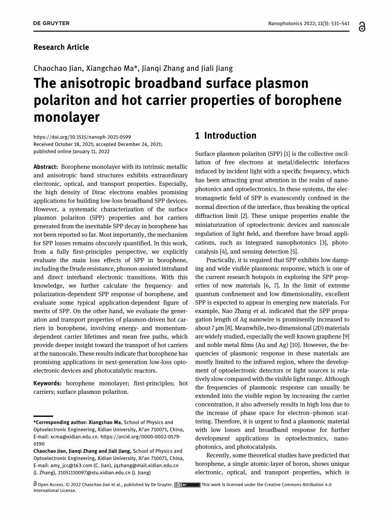
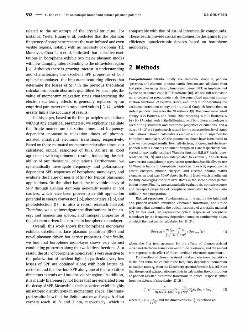
The optimized lattice structure of borophenemonolayer β12is shown in Figure 1(a). Structurally, the unit cell of bor-ophene is rectangular consisting of five atoms. Borophenehas a 47-Pmmm space group with lattices constants ofa = 2.92 Å and b = 5.06 Å, respectively, which are in goodagreement with the reported experimental values [32].Experimentally, the most stable β12 borophene has beensynthesized onAg substrate [33, 34]. Moreover, the phonondispersion of borophenemonolayer in Figure 2(a) shows 15phonon branches (3 acoustic, 12 optical) with a quite highoptical phonon cut-off frequency (∼148 meV), which iscomparable with the value of 200 meV in graphene. Thisindicates that the bonding among boron atoms in bor-ophene monolayer is almost as strong as carbon–carbonbonds in graphene. Most importantly, the eigenvaluesshow that all the phonon modes have no imaginary fre-quencies, evidencing the dynamic stability of borophenemonolayer.
Figure 2(b) shows the DFT calculated band structure inthe first Brillouin zone, which is in excellent agreementwith previous calculations [35]. Interestingly, along the Γ-Xdirection, the energy band crosses the Fermi level, indi-cating metallic properties of borophene. However, alongthe Γ-Y direction, there is a direct band gap of about 2 eV.As a result, borophene monolayer is a highly anisotropic
Figure 1: Optimized lattice structures of borophene monolayer.(a) Top and side views of the optimized lattice structures ofborophene monolayer. The area enclosed by a black rectanglecorresponds to a unit cell of borophene. (b) The first Brillouin zone ofborophene monolayer, the irreducible k-point path Γ-X-M-Y-Γ-M isused for calculating its band structure and phonon spectrum.
C. Jian et al.: The anisotropic broadband surface plasmon polariton 533
metal, which has a great impact on its optical and carriertransport properties, which will be discussed in detail inthe following sections. Examining the density of states(DOS) of borophene, graphene, and Ag(111) monolayers inFigure 2(c), we find that there is a relatively large DOS nearthe Fermi level in borophene monolayer, indicating highintrinsic carrier density, which is comparable with that ofAg(111) monolayers. Naturally, 2D materials with highintrinsic carrier density may sustain plasmon in the visiblerange that is particularly desirable for optical devices.
3.2 Surface plasmon polariton (SPP)properties
The optical response of plasmonic metallic materialsacross a broad frequency range, especially in the visiblelight region, is of great interest in many fields. Here, wefocus on the SPP properties of borophene monolayer. ForSPP, the decay channels include Landau damping andresistive dissipation. Generally, the Landau damping canbe further divided into direct interband and phonon-assisted intraband electronic excitations. Physically, therelevant losses of SPP can be expressed by the imaginarypart of the dielectric function, which is related to the realpart of conductivity as
Imϵ(ω) = Reσ(ω)ϵ0ω
(7)
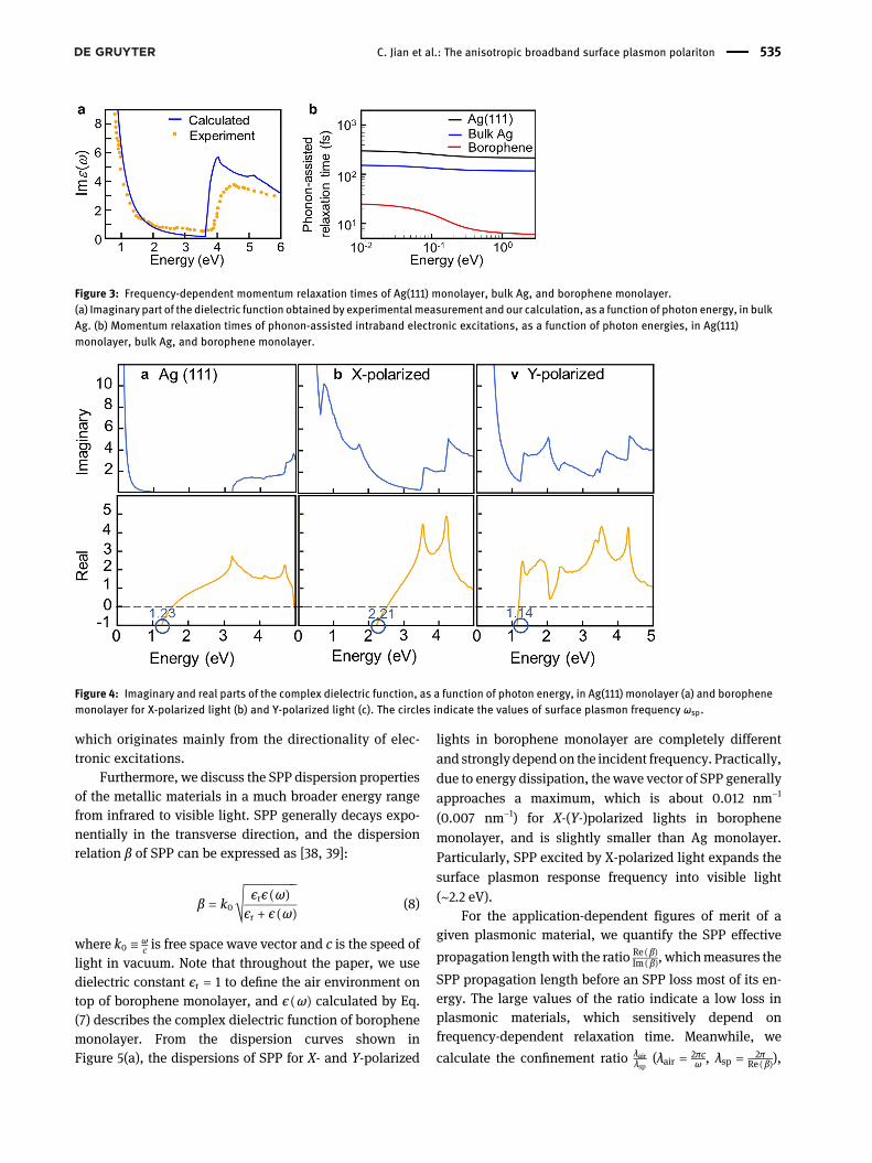
where Reσ(ω) is the real part of frequency-dependentcomplex conductivity (Eq. (1)). Then we calculate thecorresponding real part of the dielectric function usingthe Kramers–Kronig relation [36]. Firstly, to verify theaccuracy of our theoretical methods, we calculate theimaginary part of the dielectric function of bulk Ag. Asshown in Figure 3(a), our calculated results are very closeto the experimental values [37], indicating that our
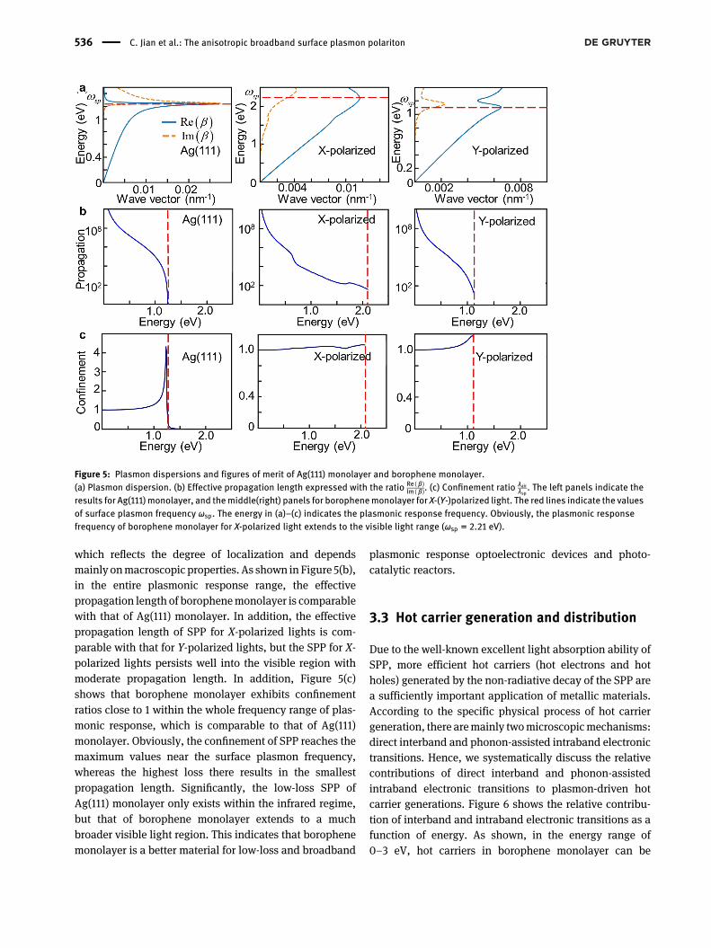
theoretical methods can provide accurate descriptions ofthe microscopic decay mechanism of SPP for metallicmaterials. Note that a slight mismatch appears withincreasing energy, which is caused by the inaccuracy ofthe PBE exchange-correlation approximation. Generally,the calculated band structures based on PBE exchange-correlation approximation tends to underestimate theinterband excitation of a material. This explains therelatively small theoretical values of the imaginary part ofdielectric function at about 3.7 eV with respect to theexperimental values. On the other hand, the PBE func-tional also slightly underestimates the dispersion of bandstructures, which increases the electronic density ofstates and thus slightly increases the theoretical values ofthe imaginary part of the dielectric function relative to theexperimental values. We plot in Figure 4 the calculatedfrequency-dependent optical dielectric function ofAg(111) and borophene monolayers across the entireinfrared–ultraviolet range. Obviously, the plasmonicdecay of borophene monolayer is higher than that of Agmonolayer in the energy range below 1 eV, where theplasmonic decay ismainly caused by the phonon-assistedintraband electronic excitations. Specifically, as shown inFigure 3(b), the phonon-assisted momentum relaxationtime of borophene monolayer is much lower than that ofAg monolayer and drops dramatically over the 0.1–0.3 eVfrequency range, originating from the existence of opticalphonon with a maximum energy ∼0.15 eV in borophenemonolayer. This indicates the larger plasmonic decay ofborophene monolayer in the low-frequency range isrelated to the relatively strong scattering with optical-phonon. Moreover, the anisotropy of plasmonic decay inborophene monolayer is very apparent in comparing Imϵfor the polarization of incoming light (Figure 4(b) versusFigure 4(c)). The results indicate that at energies less than1.6 eV, the plasmonic decay is higher for X-polarized lightthan for Y-polarized light and it is opposite above 1.6 eV,
Figure 2: Phonon dispersions and band structures of borophene monolayer.(a) Phonon dispersion and (b) band structure of borophene monolayer. The black scatters represent band structures calculated by DFTcalculations, and the red lines are obtained through interpolation of MLWFs. The green double arrow in (b) indicates the direct band gap ofabout 2 eV at Γ point. (c) Density of states (DOS) of borophene, graphene, andAg(111)monolayers (with a thickness of t2D≈ 2.36 Å) with the unitof states/eV/atom. The Fermi levels in (b) and (c) are set to 0 eV.
534 C. Jian et al.: The anisotropic broadband surface plasmon polariton
which originates mainly from the directionality of elec-tronic excitations.
Furthermore, we discuss the SPP dispersion propertiesof the metallic materials in a much broader energy rangefrom infrared to visible light. SPP generally decays expo-nentially in the transverse direction, and the dispersionrelation β of SPP can be expressed as [38, 39]:
β = k0
ϵrϵ(ω)
ϵr + ϵ(ω)
√(8)
where k0 ≡ ωc is free space wave vector and c is the speed of
light in vacuum. Note that throughout the paper, we usedielectric constant ϵr = 1 to define the air environment ontop of borophene monolayer, and ϵ(ω) calculated by Eq.(7) describes the complex dielectric function of borophenemonolayer. From the dispersion curves shown inFigure 5(a), the dispersions of SPP for X- and Y-polarized
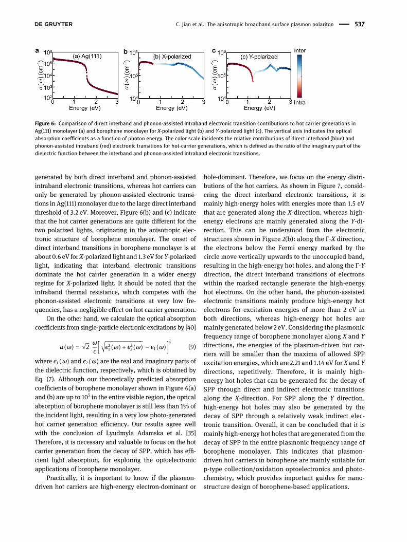
lights in borophene monolayer are completely differentand strongly depend on the incident frequency. Practically,due to energy dissipation, the wave vector of SPP generallyapproaches a maximum, which is about 0.012 nm−1
(0.007 nm−1) for X-(Y-)polarized lights in borophenemonolayer, and is slightly smaller than Ag monolayer.Particularly, SPP excited by X-polarized light expands thesurface plasmon response frequency into visible light(∼2.2 eV).
For the application-dependent figures of merit of agiven plasmonic material, we quantify the SPP effective
propagation lengthwith the ratio Re(β)Im(β), whichmeasures the
SPP propagation length before an SPP loss most of its en-ergy. The large values of the ratio indicate a low loss inplasmonic materials, which sensitively depend onfrequency-dependent relaxation time. Meanwhile, we
calculate the confinement ratio λairλsp (λair = 2πc
ω , λsp = 2πRe(β)),
Figure 3: Frequency-dependent momentum relaxation times of Ag(111) monolayer, bulk Ag, and borophene monolayer.(a) Imaginary part of the dielectric function obtained by experimentalmeasurement and our calculation, as a function of photon energy, in bulkAg. (b) Momentum relaxation times of phonon-assisted intraband electronic excitations, as a function of photon energies, in Ag(111)monolayer, bulk Ag, and borophene monolayer.
Figure 4: Imaginary and real parts of the complex dielectric function, as a function of photon energy, in Ag(111) monolayer (a) and borophenemonolayer for X-polarized light (b) and Y-polarized light (c). The circles indicate the values of surface plasmon frequency ωsp.
C. Jian et al.: The anisotropic broadband surface plasmon polariton 535
which reflects the degree of localization and dependsmainly onmacroscopic properties. As shown in Figure 5(b),in the entire plasmonic response range, the effectivepropagation length of borophenemonolayer is comparablewith that of Ag(111) monolayer. In addition, the effectivepropagation length of SPP for X-polarized lights is com-parable with that for Y-polarized lights, but the SPP for X-polarized lights persists well into the visible region withmoderate propagation length. In addition, Figure 5(c)shows that borophene monolayer exhibits confinementratios close to 1 within the whole frequency range of plas-monic response, which is comparable to that of Ag(111)monolayer. Obviously, the confinement of SPP reaches themaximum values near the surface plasmon frequency,whereas the highest loss there results in the smallestpropagation length. Significantly, the low-loss SPP ofAg(111) monolayer only exists within the infrared regime,but that of borophene monolayer extends to a muchbroader visible light region. This indicates that borophenemonolayer is a better material for low-loss and broadband
plasmonic response optoelectronic devices and photo-catalytic reactors.
3.3 Hot carrier generation and distribution
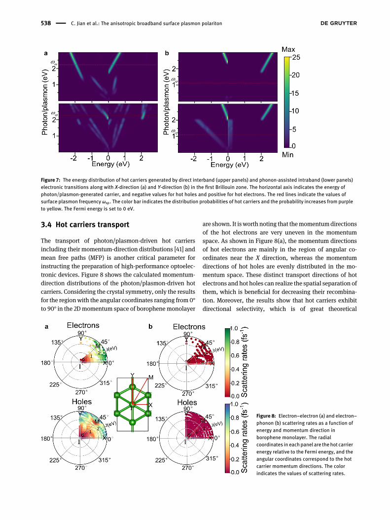
Due to the well-known excellent light absorption ability ofSPP, more efficient hot carriers (hot electrons and hotholes) generated by the non-radiative decay of the SPP area sufficiently important application of metallic materials.According to the specific physical process of hot carriergeneration, there aremainly twomicroscopicmechanisms:direct interband and phonon-assisted intraband electronictransitions. Hence, we systematically discuss the relativecontributions of direct interband and phonon-assistedintraband electronic transitions to plasmon-driven hotcarrier generations. Figure 6 shows the relative contribu-tion of interband and intraband electronic transitions as afunction of energy. As shown, in the energy range of0–3 eV, hot carriers in borophene monolayer can be
Figure 5: Plasmon dispersions and figures of merit of Ag(111) monolayer and borophene monolayer.(a) Plasmon dispersion. (b) Effective propagation length expressed with the ratio Re(β)
Im(β). (c) Confinement ratio λairλsp . The left panels indicate the
results for Ag(111) monolayer, and themiddle(right) panels for borophenemonolayer for X-(Y-)polarized light. The red lines indicate the valuesof surface plasmon frequency ωsp. The energy in (a)–(c) indicates the plasmonic response frequency. Obviously, the plasmonic responsefrequency of borophene monolayer for X-polarized light extends to the visible light range (ωsp = 2.21 eV).
536 C. Jian et al.: The anisotropic broadband surface plasmon polariton
generated by both direct interband and phonon-assistedintraband electronic transitions, whereas hot carriers canonly be generated by phonon-assisted electronic transi-tions in Ag(111) monolayer due to the large direct interbandthreshold of 3.2 eV. Moreover, Figure 6(b) and (c) indicatethat the hot carrier generations are quite different for thetwo polarized lights, originating in the anisotropic elec-tronic structure of borophene monolayer. The onset ofdirect interband transitions in borophene monolayer is atabout 0.6 eV forX-polarized light and 1.3 eV for Y-polarizedlight, indicating that interband electronic transitionsdominate the hot carrier generation in a wider energyregime for X-polarized light. It should be noted that theintraband thermal resistance, which competes with thephonon-assisted electronic transitions at very low fre-quencies, has a negligible effect on hot carrier generation.
On the other hand, we calculate the optical absorptioncoefficients from single-particle electronic excitations by [40]
α(ω) = 2√ ω
c[
ϵ21(ω) + ϵ22(ω)√
− ϵ1(ω)]12
(9)
where ϵ1(ω) and ϵ2(ω) are the real and imaginary parts ofthe dielectric function, respectively, which is obtained byEq. (7). Although our theoretically predicted absorptioncoefficients of borophene monolayer shown in Figure 6(a)and (b) are up to 105 in the entire visible region, the opticalabsorption of borophene monolayer is still less than 1% ofthe incident light, resulting in a very low photo-generatedhot carrier generation efficiency. Our results agree wellwith the conclusion of Lyudmyla Adamska et al. [35]Therefore, it is necessary and valuable to focus on the hotcarrier generation from the decay of SPP, which has effi-cient light absorption, for exploring the optoelectronicapplications of borophene monolayer.
Practically, it is important to know if the plasmon-driven hot carriers are high-energy electron-dominant or
hole-dominant. Therefore, we focus on the energy distri-butions of the hot carriers. As shown in Figure 7, consid-ering the direct interband electronic transitions, it ismainly high-energy holes with energies more than 1.5 eVthat are generated along the X-direction, whereas high-energy electrons are mainly generated along the Y-di-rection. This can be understood from the electronicstructures shown in Figure 2(b): along the Γ-X direction,the electrons below the Fermi energy marked by thecircle move vertically upwards to the unoccupied band,resulting in the high-energy hot holes, and along the Γ-Ydirection, the direct interband transitions of electronswithin the marked rectangle generate the high-energyhot electrons. On the other hand, the phonon-assistedelectronic transitions mainly produce high-energy hotelectrons for excitation energies of more than 2 eV inboth directions, whereas high-energy hot holes aremainly generated below 2 eV. Considering the plasmonicfrequency range of borophene monolayer along X and Ydirections, the energies of the plasmon-driven hot car-riers will be smaller than the maxima of allowed SPPexcitation energies, which are 2.21 and 1.14 eV for X and Ydirections, repetitively. Therefore, it is mainly high-energy hot holes that can be generated for the decay ofSPP through direct and indirect electronic transitionsalong the X-direction. For SPP along the Y direction,high-energy hot holes may also be generated by thedecay of SPP through a relatively weak indirect elec-tronic transition. Overall, it can be concluded that it ismainly high-energy hot holes that are generated from thedecay of SPP in the entire plasmonic frequency range ofborophene monolayer. This indicates that plasmon-driven hot carriers in borophene are mainly suitable forp-type collection/oxidation optoelectronics and photo-chemistry, which provides important guides for nano-structure design of borophene-based applications.
Figure 6: Comparison of direct interband and phonon-assisted intraband electronic transition contributions to hot carrier generations inAg(111) monolayer (a) and borophene monolayer for X-polarized light (b) and Y-polarized light (c). The vertical axis indicates the opticalabsorption coefficients as a function of photon energy. The color scale incidents the relative contributions of direct interband (blue) andphonon-assisted intraband (red) electronic transitions for hot-carrier generations, which is defined as the ratio of the imaginary part of thedielectric function between the interband and phonon-assisted intraband electronic transitions.
C. Jian et al.: The anisotropic broadband surface plasmon polariton 537
3.4 Hot carriers transport
The transport of photon/plasmon-driven hot carriersincluding their momentum-direction distributions [41] andmean free paths (MFP) is another critical parameter forinstructing the preparation of high-performance optoelec-tronic devices. Figure 8 shows the calculated momentum-direction distributions of the photon/plasmon-driven hotcarriers. Considering the crystal symmetry, only the resultsfor the regionwith the angular coordinates ranging from 0°to 90° in the 2Dmomentum space of borophene monolayer
are shown. It is worth noting that themomentumdirectionsof the hot electrons are very uneven in the momentumspace. As shown in Figure 8(a), the momentum directionsof hot electrons are mainly in the region of angular co-ordinates near the X direction, whereas the momentumdirections of hot holes are evenly distributed in the mo-mentum space. These distinct transport directions of hotelectrons and hot holes can realize the spatial separation ofthem, which is beneficial for decreasing their recombina-tion. Moreover, the results show that hot carriers exhibitdirectional selectivity, which is of great theoretical
Figure 8: Electron–electron (a) and electron–phonon (b) scattering rates as a function ofenergy and momentum direction inborophene monolayer. The radialcoordinates in eachpanel are thehot carrierenergy relative to the Fermi energy, and theangular coordinates correspond to the hotcarrier momentum directions. The colorindicates the values of scattering rates.
Figure 7: The energy distribution of hot carriers generated by direct interband (upper panels) and phonon-assisted intraband (lower panels)electronic transitions along with X-direction (a) and Y-direction (b) in the first Brillouin zone. The horizontal axis indicates the energy ofphoton/plasmon-generated carrier, and negative values for hot holes and positive for hot electrons. The red lines indicate the values ofsurface plasmon frequency ωsp. The color bar indicates the distribution probabilities of hot carriers and the probability increases from purpleto yellow. The Fermi energy is set to 0 eV.
538 C. Jian et al.: The anisotropic broadband surface plasmon polariton
guidance for hot carrier-based applications, such as directphotoelectric conversion on the surface of borophenemonolayer or hot carrier injection into the contactsemiconductor.
The lifetimes and mean free paths of hot carriers arecalculated by fully considering both electron–electron andelectron–phonon scattering processes. As expected for ametallic material conforming to Fermi-liquid theory [42],the electron–electron scattering rates shown in Figure 8(a)dominate far away from the Fermi energy due to amuch larger phase space for such scattering events [43].Meanwhile, electron–phonon scattering rates shown inFigure 8(b) play amajor role near the Fermi energy, and thecalculated values agree well with the results of LyudmylaAdamska et al. [35] Moreover, the values of electron–phonon scattering rates in borophene monolayer, whichare mainly distributed within about 0.5 fs−1, have the sameorder-of-magnitude as the electron–electron scatteringrates. This indicates that electron–phonon scattering issufficiently important compared with electron–electronscattering. Therefore, the effects of electron–phononscattering on the hot carrier transport properties cannot beignored, which is different from the general assumptionthat electron–phonon scattering occurs on a very slow timescale [42].
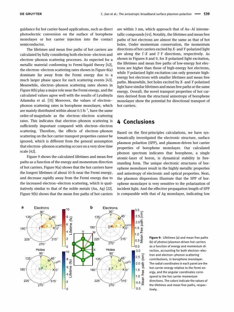
Figure 9 shows the calculated lifetimes and mean freepaths as a function of the energy and momentum direction
of hot carriers. Figure 9(a) shows that the hot carriers havethe longest lifetimes of about 10 fs near the Fermi energy,and decrease rapidly away from the Fermi energy due tothe increased electron–electron scattering, which is qual-
itatively similar to that of the noble metals (Au, Ag) [22].Figure 9(b) shows that the mean free paths of hot carriers
are within 3 nm, which approach that of Au–Al interme-tallic compounds [44]. Notably, the lifetimes andmean freepaths of hot electrons are almost the same as that of hotholes. Under momentum conservation, the momentumdirections of hot carriers excited byX- andY-polarized lightare along the Γ-X and Γ-Y directions, respectively. Asshown in Figures 8 and 9, for X-polarized light excitation,the lifetimes and mean free paths of low-energy hot elec-trons are higher than those of high-energy hot electrons,while Y-polarized light excitation can only generate high-energy hot electrons with smaller lifetimes and mean freepaths. Meanwhile, hot holes excited by X- and Y-polarizedlight have similar lifetimes andmean free paths at the sameenergy. Overall, the novel transport properties of hot car-riers derived from the structural anisotropy of borophenemonolayer show the potential for directional transport ofhot carriers.
4 Conclusions
Based on the first-principles calculations, we have sys-tematically investigated the electronic structure, surfaceplasmon polariton (SPP), and plasmon-driven hot carrierproperties of borophene monolayer. Our calculatedphonon spectrum indicates that borophene, a singleatomic-layer of boron, is dynamical stability in free-standing form. The unique electronic structures of bor-ophene monolayer result in the highly metallic propertiesand anisotropy of electronic and optical properties. Next,the plasmon dispersions illustrate that the SPP of bor-ophene monolayer is very sensitive to the polarization ofincident light. And the effective propagation length of SPPis comparable with that of Ag monolayer, indicating low
Figure 9: Lifetimes (a) and mean free paths(b) of photon/plasmon-driven hot carriersas a function of energy and momentum di-rection, accounting for both electron–elec-tron and electron–phonon scatteringcontributions, in borophene monolayer.The radial coordinates in each panel are thehot carrier energy relative to the Fermi en-ergy, and the angular coordinates corre-spond to the hot carrier momentumdirections. The colors indicate the values ofthe lifetimes and mean free paths, respec-tively.
C. Jian et al.: The anisotropic broadband surface plasmon polariton 539
losses of SPP in borophene monolayer. In particular,the low losses SPP of borophene monolayer under theX-polarized incident light extendswell into the visible lightregime. This result informs a material selection for lowlosses and broadband plasmonic response optoelectronicdevices and photocatalytic reactors. Finally, the plasmon-driven hot carriers exhibit high anisotropy in momentumspaces, and it is mainly high-energy hot holes that aregenerated from the decay of SPP, which are instructionalfor designing applications that require carriers of specificmomentum and energy and efficiently collecting hot holesin borophene monolayer. Moreover, the lifetime and meanfree path of hot carriers reach 10 fs and 3 nm, respectively,which approach that of Au and Al compounds. As a result,we expect that the reported results will motivate furtherefforts to achieve low-loss broadband optical response anddirectional carrier transport in next-generation plasmonicoptoelectronic devices and photocatalytic reactors.
Author contributions: All the authors have acceptedresponsibility for the entire content of this submittedmanuscript and approved submission.Research funding: This work is supported by theNational Natural Science Foundation of China (11704298,61904138), the China Postdoctoral Science Foundation(2019M653549), the 2018 Postdoctoral Innovation TalentSupport Program of China (BX20180233), and the 111Project of China (B17035). The authors thank Prof.Ravishankar Sundararaman (Rensselaer PolytechnicInstitute) for fruitful discussions on the calculation offrequency-dependent momentum relaxation times ofphonon-assisted intraband electronic excitations on 2Dplasmonic materials and the details using JDFTx software.Conflict of interest statement: The authors declare noconflicts of interest regarding this article.
References
[1] R. W. Heeres, L. P. Kouwenhoven, and V. Zwiller, “Quantuminterference in plasmonic circuits,” Nat. Nanotechnol., vol. 8,no. 10, pp. 719–722, 2013.
[2] W. J. Zhang, L. Gao, H. Wei, and H. X. Xu, “Modulation ofpropagating surface plasmons,” Acta Phys. Sin., vol. 68, no. 14,p. 147302, 2019.
[3] J. A. Schuller, E. S. Barnard, W. Cai, Y. C. Jun, J. S. White, andM. L. Brongersma, “Erratum: plasmonics for extreme lightconcentration and manipulation,” Nat. Mater., vol. 9, no. 4,2010, p. 368.
[4] C. Clavero, “Plasmon-induced hot-electron generation atnanoparticle/metal-oxide interfaces for photovoltaic andphotocatalytic devices,” Nat. Photonics, vol. 8, no. 2,pp. 95–103, 2014.
[5] J. Jiang, X. Wang, S. Li, et al., “Plasmonic nano-arrays forultrasensitive bio-sensing,” Nanophotonics, vol. 7, no. 9,pp. 1517–1531, 2018.
[6] H. Su, S. Wu, Y. Yang, et al., “Surface plasmon polariton-enhanced photoluminescence of monolayer MoS2 onsuspended periodic metallic structures,” Nanophotonics,vol. 10, no. 2, pp. 975–982, 2020.
[7] M. Gao, Y. He, Y. Chen, et al., “Tunable surface plasmonpolaritons and ultrafast dynamics in 2D nanohole arrays,”Nanoscale, vol. 11, no. 35, pp. 16428–16436, 2019.
[8] N. Zhang, T. Fu, H. Xu, and W. Wang, “Reduced loss of plasmonpropagation in a Ag nanowire on Si substrate,” Nano Energy,vol. 68, p. 104322, 2020.
[9] T. J. Echtermeyer, S. Milana, U. Sassi, et al., “Surface plasmonpolariton graphene photodetectors,” Nano Lett., vol. 16, no. 1,pp. 8–20, 2016.
[10] X. Xue, Y. Fan, E. Segal, et al., “Periodical concentration ofsurface plasmon polaritons by wave interference in metallic filmwith nanocavity array,” Mater. Today, vol. 46, pp. 54–61, 2021.
[11] Y. Huang, S. N. Shirodkar, and B. I. Yakobson, “Two-dimensionalboron polymorphs for visible range plasmonics: a first-principles exploration,” J. Am. Chem. Soc., vol. 139, no. 47,pp. 17181–17185, 2017.
[12] C. Lian, S. Q. Hu, J. Zhang, et al., “Integrated plasmonics:broadband Dirac plasmons in borophene,” Phys. Rev. Lett.,vol. 125, no. 11, p. 116802, 2020.
[13] T. Zhou, P. Zheng, S. C. Pandey, R. Sundararaman, and D. Gall,“The electrical resistivity of rough thin films: a model based onelectron reflection at discrete step edges,” J. Appl. Phys.,vol. 123, no. 15, p. 155107, 2018.
[14] R. A. Maniyara, D. Rodrigo, R. Yu, et al., “Tunable plasmons inultrathin metal films,” Nat. Photonics, vol. 13, no. 5,pp. 328–333, 2019.
[15] R. Sundararaman, P. Narang, A. S. Jermyn, W. A. Goddard 3rd,and H. A. Atwater, “Theoretical predictions for hot-carriergeneration from surface plasmon decay,” Nat. Commun., vol. 5,p. 5788, 2014.
[16] J. U. Salmón-Gamboa, M. Romero-Gómez, D. J. Roth, et al.,“Rational design of bimetallic photocatalysts based onplasmonically-derived hot carriers,” Nanoscale Adv., vol. 3,no. 3, pp. 767–780, 2021.
[17] N. S. Sitaraman, M. M. Kelley, R. D. Porter, et al., “Effect of thedensity of states at the Fermi level on defect free energies andsuperconductivity: a case study of Nb3Sn,”Phys. Rev. B, vol. 103,no. 11, p. 115106, 2021.
[18] R. Sundararaman, K. Letchworth-Weaver, K. A. Schwarz,D. Gunceler, Y. Ozhabes, and T. A. Arias, “JDFTx: software for jointdensity-functional theory,” Software, vol. 6, pp. 278–284, 2017.
[19] R. Sundararaman and T. A. Arias, “Regularization of the Coulombsingularity in exact exchange by wigner-seitz truncatedinteractions: towards chemical accuracy in nontrivial systems,”Phys. Rev. B, vol. 87, no. 16, p. 165122, 2013.
[20] I. Souza, N. Marzari, and D. Vanderbilt, “Maximally localizedwannier functions for entangled energy bands,” Phys. Rev. B,vol. 65, no. 3, 2001, Art no. 035109.
[21] F. Giustino, M. L. Cohen, and S. G. Louie, “Electron-phononinteraction using wannier functions,” Phys. Rev. B, vol. 76,no. 16, p. 165108, 2007.
[22] A. M. Brown, R. Sundararaman, P. Narang, W. A. Goddard 3rd,and H. A. Atwater, “Nonradiative plasmon decay and hot carrier
540 C. Jian et al.: The anisotropic broadband surface plasmon polariton
dynamics: effects of phonons, surfaces, and geometry,” ACSNano, vol. 10, no. 1, pp. 957–966, 2016.
[23] R. Sundararaman, T. Christensen, Y. Ping, et al., “Plasmonics inargentene,” Phys. Rev. Mat., vol. 4, no. 7, 2020, Art no. 074011.
[24] A. Vakil and N. Engheta, “Transformation optics usinggraphene,” Science, vol. 332, no. 6035, pp. 1291–1294, 2011.
[25] D. Haberer, L. Petaccia, A. V. Fedorov, et al., “AnisotropicEliashberg function and electron-phonon coupling in dopedgraphene,” Phys. Rev. B, vol. 88, no. 8, 2013, Art no. 081401(R).
[26] P. B. Allen, “Electron-phonon effects in the infrared properties ofmetals,” Phys. Rev. B, vol. 3, no. 2, pp. 305–320, 1971.
[27] C. A. C. Garcia, J. Coulter, and P. Narang, “Optoelectronicresponse of the type-I weyl semimetals TaAs and NbAsfrom first principles,” Phys. Rev. Res., vol. 2, no. 1, 2020,Art no. 013073.
[28] A. Habib, F. Florio, and R. Sundararaman, “Hot carrier dynamicsin plasmonic transition metal nitrides,” J. Opt., vol. 20, no. 6,p. 105130, 2018.
[29] P. Narang, R. Sundararaman, A. S. Jermyn, W. A. Goddard, andH. A. Atwater, “Cubic nonlinearity driven up-conversion in high-field plasmonic hot carrier systems,” J. Phys. Chem. C, vol. 120,no. 37, pp. 21056–21062, 2016.
[30] M. Bernardi, D. Vigil-Fowler, C. S. Ong, J. B. Neaton, andS. G. Louie, “Ab initio study of hot electrons in GaAs,” Proc. Natl.Acad. Sci. Unit. States Am., vol. 112, no. 17, pp. 5291–5296, 2015.
[31] C. Jian, X. Ma, J. Zhang, and X. Yong, “Strained MoSi2N4monolayers with excellent solar energy absorption and carriertransport properties,” J. Phys. Chem. C, vol. 125, no. 28,pp. 15185–15193, 2021.
[32] B. Feng, J. Zhang, Q. Zhong, et al., “Experimental realization oftwo-dimensional boron sheets,” Nat. Chem., vol. 8, no. 6,pp. 563–568, 2016.
[33] Y. Tian, Z. Guo, T. Zhang, et al., “Inorganic boron-basednanostructures: synthesis, optoelectronic properties, andprospective applications,” Nanomaterials, vol. 9, no. 4, p. 538,2019.
[34] P. Ranjan, T. K. Sahu, R. Bhushan, et al., “Freestandingborophene and its hybrids,” Adv. Mater., vol. 31, no. 27, 2019,Art no. e1900353.
[35] L. Adamska, S. Sadasivam, J. J. Foley, P. Darancet, andS. Sharifzadeh, “First-principles investigation of borophene as amonolayer transparent conductor,” J. Phys. Chem. C, vol. 122,no. 7, pp. 4037–4045, 2018.
[36] K. S. B. De Silva, A. Gentle, M. Arnold, V. J. Keast, andM. B. Cortie, “Dielectric function and its predicted effect onlocalized plasmon resonances of equiatomic Au–Cu,” J. Phys. DAppl. Phys., vol. 48, no. 21, p. 215304, 2015.
[37] M. Xu, J. Y. Yang, S. Zhang, and L. Liu, “Role of electron-phononcoupling in finite-temperature dielectric functions of Au, Ag, andCu,” Phys. Rev. B, vol. 96, no. 11, p. 115154, 2017.
[38] M. Jablan, M. Soljacic, and H. Buljan, “Plasmons in graphene:fundamental properties and potential applications,” Proc. IEEE,vol. 101, no. 7, pp. 1689–1704, 2013.
[39] Z. Y. Zhang, H. Y. Wang, J. L. Du, et al., “Surface plasmon-modulated fluorescence on 2D metallic silver gratings,” IEEEPhoton. Technol. Lett., vol. 27, no. 8, pp. 821–823, 2015.
[40] C. c. Jian, J. Zhang, and X. Ma, “Cu-Ag alloy for engineeringproperties and applications based on the LSPR of metalnanoparticles,” RSC Adv., vol. 10, no. 22, pp. 13277–13285, 2020.
[41] J. B. Khurgin, “Hot carriers generated by plasmons: where arethey generated and where do they go from there?” FaradayDiscuss., vol. 214, pp. 35–58, 2019.
[42] P. M. Echenique, J. M. Pitarke, E. V. Chulkov, and A. Rubio,“Theory of inelastic lifetimes of low-energy electrons in metals,”Chem. Phys., vol. 251, pp. 1–35, 2000.
[43] F. Ladstädter, U.Hohenester, P. Puschnig, andC. Ambrosch-Draxl,“First-principles calculation of hot-electron scattering in metals,”Phys. Rev. B, vol. 70, no. 23, p. 235125, 2004.
[44] C. Jian, J. Zhang, W. He, and X. Ma, “Au-Al intermetalliccompounds: a series of more efficient LSPR materials for hotcarriers-based applications than noble metal Au,” Nano Energy,vol. 82, p. 105763, 2021.
C. Jian et al.: The anisotropic broadband surface plasmon polariton 541
Related Documents