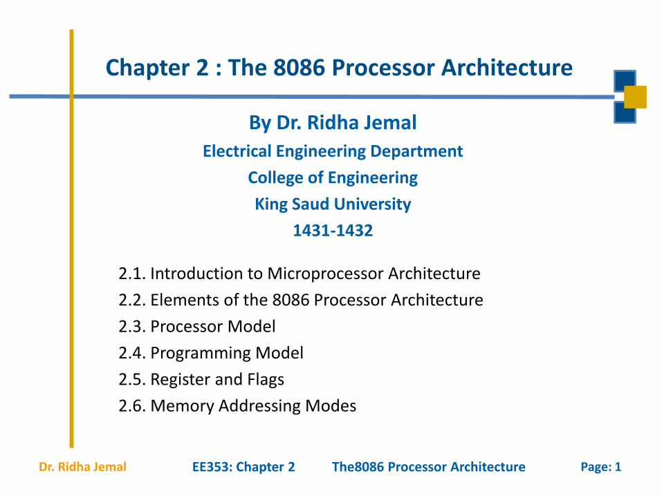
Page: 1 Dr. Ridha Jemal Chapter 2 : The 8086 Processor Architecture 2.1. Introduction to Microprocessor Architecture 2.2. Elements of the 8086 Processor Architecture 2.3. Processor Model 2.4. Programming Model 2.5. Register and Flags 2.6. Memory Addressing Modes By Dr. Ridha Jemal Electrical Engineering Department College of Engineering King Saud University 1431-1432 EE353: Chapter 2 The8086 Processor Architecture

The 8086 Micro Processor Architecture By Dr. RidhaJemal
Jul 15, 2015
Welcome message from author
This document is posted to help you gain knowledge. Please leave a comment to let me know what you think about it! Share it to your friends and learn new things together.
Transcript
Page: 1Dr. Ridha Jemal
Chapter 2 : The 8086 Processor Architecture
2.1. Introduction to Microprocessor Architecture
2.2. Elements of the 8086 Processor Architecture
2.3. Processor Model
2.4. Programming Model
2.5. Register and Flags
2.6. Memory Addressing Modes
By Dr. Ridha JemalElectrical Engineering Department
College of Engineering
King Saud University
1431-1432
EE353: Chapter 2 The8086 Processor Architecture

Page: 2Dr. Ridha Jemal
A computer whose entire CPU is contained on one integrated circuits.The important characteristics of a microprocessor are the widths of itsinternal and external address bus and data bus (and instruction), its clockrate and its instruction set.
CPU : The part of a computer which controls all the other parts. The CPUfetches instructions from memory, decodes and executes them. This maycause it to transfer data to or from memory or to activate peripherals toperform input or output.
Microprocessor:
The connections between the CPU and memory input/output whichcarry the address from/to which the CPU wishes to read or write. Thenumber of bits of address bus determines the maximum size of memorywhich the processor can access.
Address Bus:
Introduction to Microprocessor Architecture
EE353: Chapter 2 The8086 Processor Architecture

Page: 3Dr. Ridha Jemal
One of a small number of high-speed memory locations in acomputer's CPU.
Register:
A data storage device for which the order of access to differentlocations does not affect the speed of access. The term "RAM" hasgained the additional meaning of read-write. Most kinds ofsemiconductor read-only memory (ROM) are actually "random access"in the above sense but are never referred to as RAM. Furthermore,memory referred to as RAM can usually be read and written equallyquickly (approximately), in contrast to the various kinds ofprogrammable read-only memory. Finally, RAM is usually volatile
Random Access Memory (RAM):
Introduction to Microprocessor Architecture
EE353: Chapter 2 The8086 Processor Architecture
Page: 4Dr. Ridha Jemal
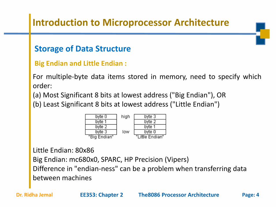
Storage of Data Structure
For multiple-byte data items stored in memory, need to specify whichorder:(a) Most Significant 8 bits at lowest address ("Big Endian"), OR (b) Least Significant 8 bits at lowest address ("Little Endian")
Little Endian: 80x86 Big Endian: mc680x0, SPARC, HP Precision (Vipers) Difference in "endian-ness" can be a problem when transferring data between machines
Big Endian and Little Endian :
Introduction to Microprocessor Architecture
EE353: Chapter 2 The8086 Processor Architecture

Page: 5Dr. Ridha Jemal
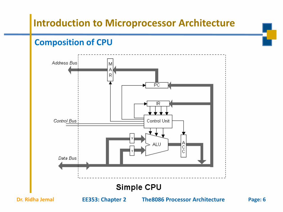
Composition of CPU
REGISTERSInstruction Pointer Counter : Holds address of instruction being executed
Instruction Register: Holds instruction while it's decoded/executed
Stack Pointer: Address of top of stack
Accumulator: Result of ALU operations
General-Purpose Registers : Hold temporary results or addresses during execution of instructions Write results to memory
Introduction to Microprocessor Architecture
EE353: Chapter 2 The8086 Processor Architecture
CONTROL UNIT Generates control/timing signals Controls decoding/execution of instructions
ALUUsed during execution of instructions Mathematical operations: * / + - etc. Logical operations: shift, rotate
Page: 6Dr. Ridha Jemal
Composition of CPU
Introduction to Microprocessor Architecture
EE353: Chapter 2 The8086 Processor Architecture

Page: 7Dr. Ridha Jemal
Instruction Execution
Introduction to Microprocessor Architecture
performs Fetch/Decode/Execute cycle • Fetch instruction from primary memory • Increment Program Counter • Decode • Fetch operands from memory • Execute instruction • Write results to memory
Fetch Time depends on • Access time of primary memory • Activity on System Bus
Decode/Execute Time taken depends on • System Clock speed (frequency) • Type of instruction
EE353: Chapter 2 The8086 Processor Architecture
Page: 8Dr. Ridha Jemal
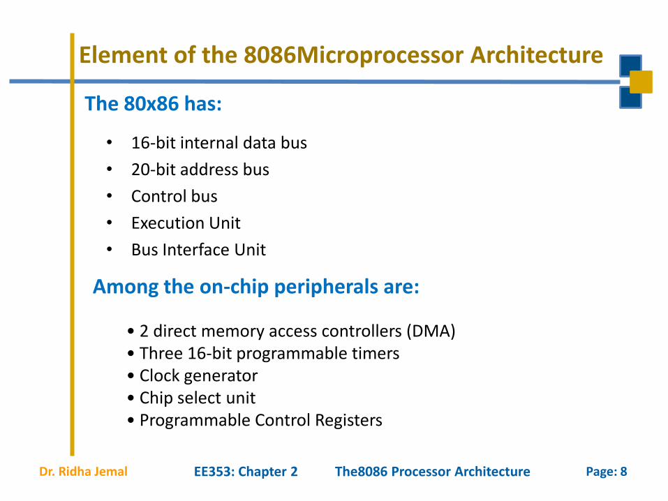
Element of the 8086Microprocessor Architecture
The 80x86 has:
• 16-bit internal data bus
• 20-bit address bus
• Control bus
• Execution Unit
• Bus Interface Unit
Among the on-chip peripherals are:
• 2 direct memory access controllers (DMA)• Three 16-bit programmable timers• Clock generator• Chip select unit• Programmable Control Registers
EE353: Chapter 2 The8086 Processor Architecture

Page: 9Dr. Ridha Jemal
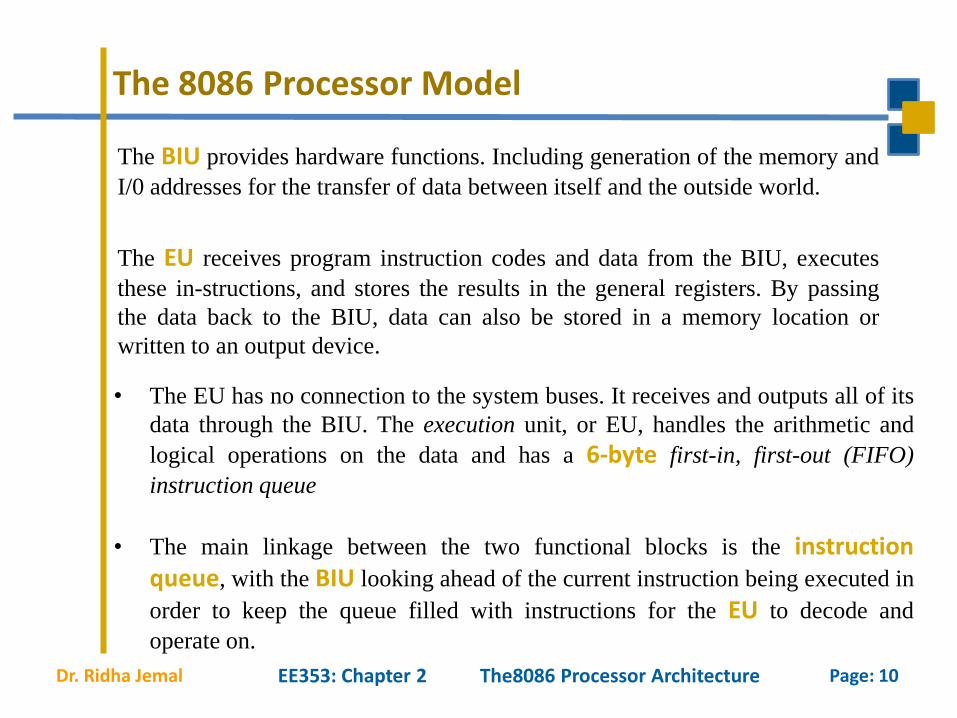
The 8086 Processor Model
BIUEU
Block Diagram ArchitectureThe simplified block diagram of the 80x86 processor model is organizedas two separate processors :
Bus Interface Unit (BIU)
Execution Unit (EU).
EE353: Chapter 2 The8086 Processor Architecture
Page: 10Dr. Ridha Jemal
The BIU provides hardware functions. Including generation of the memory and
I/0 addresses for the transfer of data between itself and the outside world.
The EU receives program instruction codes and data from the BIU, executes
these instructions, and stores the results in the general registers. By passing
the data back to the BIU, data can also be stored in a memory location or
written to an output device.
• The main linkage between the two functional blocks is the instructionqueue, with the BIU looking ahead of the current instruction being executed in
order to keep the queue filled with instructions for the EU to decode and
operate on.
• The EU has no connection to the system buses. It receives and outputs all of its
data through the BIU. The execution unit, or EU, handles the arithmetic and
logical operations on the data and has a 6-byte first-in, first-out (FIFO)
instruction queue
EE353: Chapter 2 The8086 Processor Architecture
The 8086 Processor Model

Page: 11Dr. Ridha Jemal
The organization of the processor into a separate BIU and EU allows the fetch and
execute cycles to overlap. To see this, consider what happens when the 8086 is
first started. in Figure 3.2.
The Fetch and Execute Cycle
1. The BIU outputs the contents of the instruction pointer register (IP) onto the
address bus, causing the selected byte or word in memory to be read into the BIU.
2. Register IP is incremented by one to prepare for the next instruction fetch.
3. Once inside the BIU, the instruction is passed to the queue: a first-in/first-out
storage register sometimes likened to a pipeline.
4. Assuming that the queue is initially empty, the EU immediately draws this
instruction from the queue and begins execution.
5. While the EU is executing this instruction, the BIU proceeds to fetch a new
instruction. Depending on the execution time of the first instruction, the BIU may
fill the queue with several new instructions before the EU is ready to draw its next
instruction.
6. The cycle continues, with the BIU filling the queue with instructions and the EU
fetching and executing these instructions.
EE353: Chapter 2 The8086 Processor Architecture
The 8086 Processor Model

Page: 12Dr. Ridha Jemal
The Fetch and Execute Cycle (contd.)
EE353: Chapter 2 The8086 Processor Architecture
The BIU is programmed to fetch a new instruction whenever the queue has room
for two additional bytes. The advantage to this pipelined architecture is that the
EU can execute instructions (almost) continually instead of having to wait for the
BIU to fetch a new instruction. This is shown schematically in the following
Figure.
The 8086 Processor Model
Page: 13Dr. Ridha Jemal
The “Wait” mode
EE353: Chapter 2 The8086 Processor Architecture
There are three conditions that will cause the EU to enter a "wait" mode.
• When an instruction requires access to a memory location. The BIU must
suspend fetching instructions and output the address of this memory
location. After waiting for the memory access, the EU can resume executing
instruction codes from the queue, and the BIU can resume filling the queue.
• When the instruction to be executed is a jump instruction. In this case,
control is to be transferred to a new address. The EU must wait while the
instruction at the jump address is fetched. Any bytes presently in the queue
must be discarded (they are overwritten).
• During the execution of slow-executing instructions.
The 8086 Processor Model
Page: 14Dr. Ridha Jemal
1978: The 8086 was one of the earliest 16-bit processors.
The 80286 is also a 16-bit microprocessor
Motorola 68000 is also a 16-bit microprocessor
Mid 1980’s : 32-bit microprocessors
Intel 80386, 80486 , Motorola 68030
EE353: Chapter 2 The8086 Processor Architecture
Microprocessors Timeline:
1997: The Pentium II is superscalar, supports multiprocessing, and includes
special instructions for multimedia applications.
2002:The Pentium 4 runs at insane clock rates (3.06 GHz), implements
extended multimedia instructions and has a large on-chip cache.
Internal Architecture may be different from size of Data Bus Intel 8088: internally 16-bit, 8-bit data bus
Intel 386sx: internally 32-bit, 16-bit data bus
Can build computer using cheaper external parts (eg. I/O interfaces)
The 8086 Processor Model

Page: 15Dr. Ridha Jemal
Instruction Set: operations, addressing modes
Registers: size, number
Address bus : size (number of bits)
Data bus: size
Control bus: functions
Permissible clock speeds
EE353: Chapter 2 The8086 Processor Architecture
Microprocessors Difference:
What About the 8088?
The only significant difference between the 8088 microprocessor and the
8086 microprocessor is the BIU. In the 8088, the BIU data bus path is 8 bits
wide Where the 8086 BIU data bus is l6-bit. Another difference is that the
8088 instruction queue is four bytes long instead of six.
In practice, however, the 8088 is found to only be about 30 percent slower
than an 8086.
The 8086 Processor Model
Page: 16Dr. Ridha Jemal
The 8086 Programming Model
EE353: Chapter 2 The8086 Processor Architecture
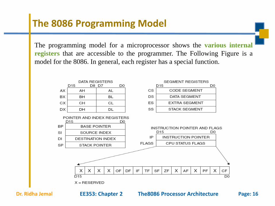
The programming model for a microprocessor shows the various internal
registers that are accessible to the programmer. The Following Figure is a
model for the 8086. In general, each register has a special function.

Page: 17Dr. Ridha Jemal EE353: Chapter 2 The8086 Processor Architecture
The eight, 16-bit general purpose registers are used for arithmetic and logical
operations.
Data Registers
Examples
MOV AL,6D -- Place the immediate hexadecimal value 6D into register AL
MOV DH,25 -- Place the immediate hexadecimal value 25 into register DH
MUL DH -- Multiply AL by DH and store the result into AX.
The four data registers labeled AX, BX, CX and DX may be further subdivided for
8-bit operations into a high-byte or low-byte register, depending where the byte is
to be stored in the register. Thus, for byte operations, the registers may be
individually addressed. So, each of these is 16 bits wide but can be accessed as a
byte or a word.
AX : known as an accumulator is used in arithmetic and logical operations
BX : refers to refers to the 16-bit base register
CX : is used as a counter
DX : may
The 8086 Programming Model
Page: 18Dr. Ridha Jemal EE353: Chapter 2 The8086 Processor Architecture
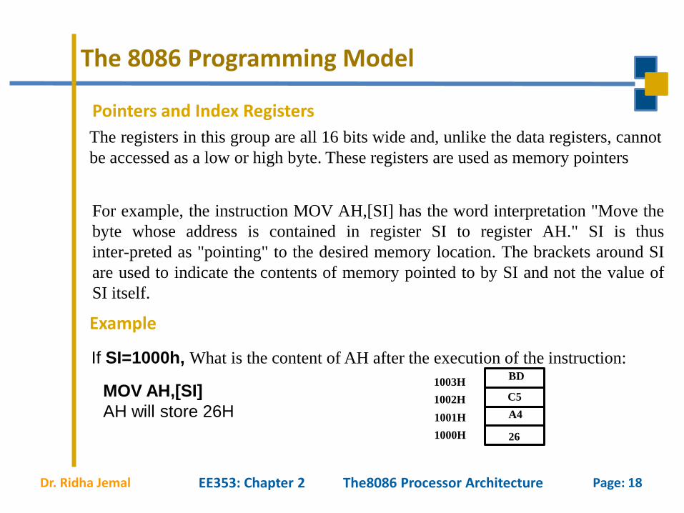
Example
If SI=1000h, What is the content of AH after the execution of the instruction:
The registers in this group are all 16 bits wide and, unlike the data registers, cannot
be accessed as a low or high byte. These registers are used as memory pointers
Pointers and Index Registers
For example, the instruction MOV AH,[SI] has the word interpretation "Move the
byte whose address is contained in register SI to register AH." SI is thus
interpreted as "pointing" to the desired memory location. The brackets around SI
are used to indicate the contents of memory pointed to by SI and not the value of
SI itself.
MOV AH,[SI]
AH will store 26H
1000H
1001H
1002H
1003H
26
A4
C5
BD
The 8086 Programming Model

Page: 19Dr. Ridha Jemal EE353: Chapter 2 The8086 Processor Architecture
The following Figure shows the bit definitions for the 16-bit flag register.
• Six of the flags are status indicators reflecting properties of the result of the last
arithmetic or logical instruction
• 8086 flag word. DF, IF, and TF can be set or reset to control the operation of
the processor
• The remaining flags are status indicators. Bits marked X are undefined.
;7FH + 1 = 80H
;there is no carry out of bit 7
;S0H has an odd number of logic ones
;there is a carry out of bit 3 into bit 4
;the result is not 0
;bit seven is 1
;the sign bit has changed
AL=80H
CF=0
PF=0
AF=l
ZF=0
SF=l
OF=l
Example
The 8086 Programming Model

Page: 20Dr. Ridha Jemal EE353: Chapter 2 The8086 Processor Architecture
Bit
PositionName Function
0 CFCarry flag: Set on high-order bit carry or borrow; cleared otherwise
2 PFParity flag: Set if low-order 8 bits of result contain an even number of 1 bits; cleared
otherwise
4 AFSet on carry from or borrow to the low-order 4 bits of the result; cleared otherwise
6 ZFZero flag: Set if result is zero; cleared otherwise
7 SFSign flag: Set equal to high-order bit of result
(0 is positive, I is negative)
8 TF
Single-step flag: Once set, a single-step interrupt
occurs after the next instruction executes; TF
is cleared by the single-step interrupt
9 IF
Interrupt-enable flag: When set, maskable
interrupts will cause the CPU to transfer control
to an interrupt vector-specified location
10 DF
Direction flag: Causes string instructions to autodecrement the appropriate index
register when set; clearing DF causes auto-increment
11 OF
Overflow flag: Set if the signed result cannot be expressed within the number of bits
in the destination operand; cleared otherwise
Status and Control Flags
The 8086 Programming Model

Page: 21Dr. Ridha Jemal EE353: Chapter 2 The8086 Processor Architecture
Central Processing Unit:
CS:IP DS:SI OR DS:DI OR DS:BX SS:SP OR SS:BP
The 8086 Programming Model

Page: 22Dr. Ridha Jemal EE353: Chapter 2 The8086 Processor Architecture
Pointers and Index Registers:
In 8086-based System, we can access 220= 1M memory locations at most
µproc
8086
20 bits (A0-A19)
16 bits (D0- D15)
Address Bus
Data Bus
Control Bus
Proc
8086
The 8086 Programming Model

Page: 23Dr. Ridha Jemal EE353: Chapter 2 The8086 Processor Architecture
IP Register:
The Instruction Pointer register (IP)
contains the offset address of the next
sequential instruction to be executed.
Thus, the IP register cannot be directly
modified.
These register descriptions have slowly
been introducing us to a new way of
addressing memory, called:
segment-offset addressing.
The segment register is used to point to
the beginning of any one of the 64K
sixteen-byte boundaries
00000H
FFFFFH
7000HSegment address
0000H
FFFFH
….
Physical Address
64 K
The 8086 Programming Model
Page: 24Dr. Ridha Jemal
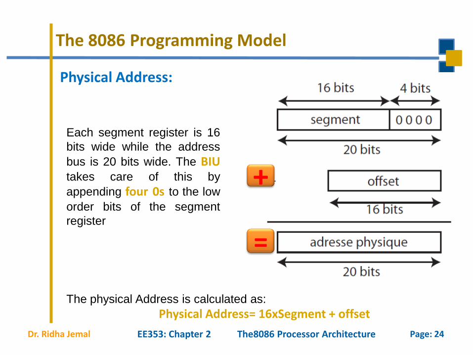
Physical Address:
EE353: Chapter 2 The8086 Processor Architecture
Each segment register is 16
bits wide while the address
bus is 20 bits wide. The BIUtakes care of this by
appending four 0s to the low
order bits of the segment
register
The physical Address is calculated as:
Physical Address= 16xSegment + offset
+
=
The 8086 Programming Model
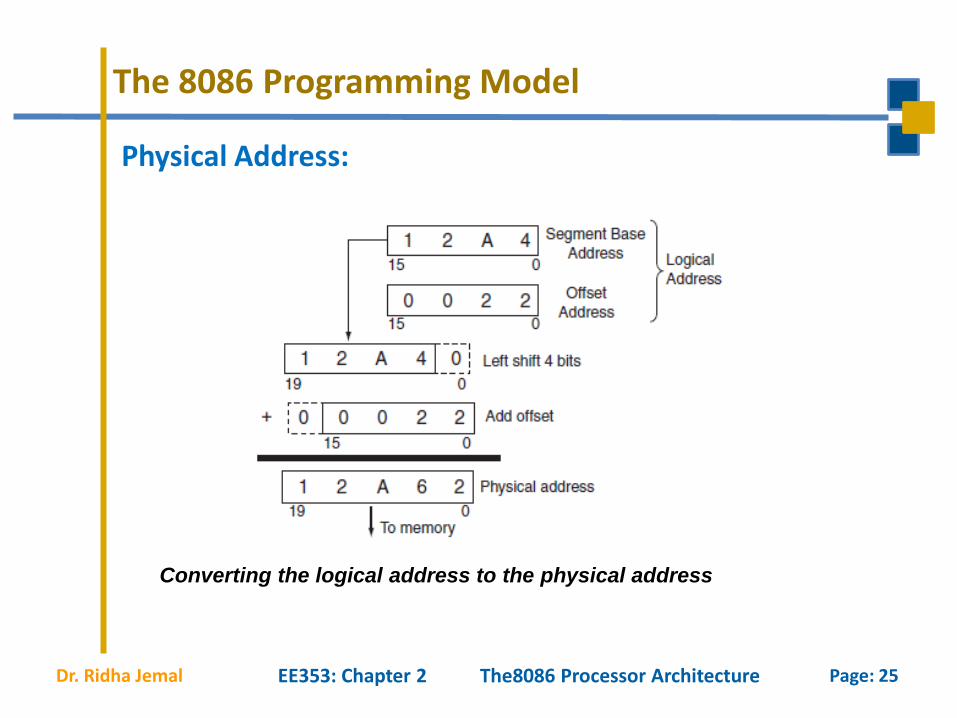
Page: 25Dr. Ridha Jemal EE353: Chapter 2 The8086 Processor Architecture
Physical Address:
Converting the logical address to the physical address
The 8086 Programming Model
Page: 26Dr. Ridha Jemal EE353: Chapter 2 The8086 Processor Architecture
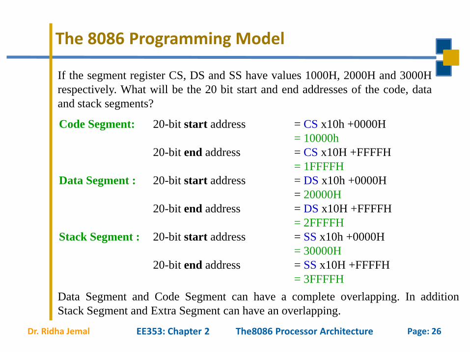
If the segment register CS, DS and SS have values 1000H, 2000H and 3000H
respectively. What will be the 20 bit start and end addresses of the code, data
and stack segments?
Code Segment: 20-bit start address = CS x10h +0000H
= 10000h
20-bit end address = CS x10H +FFFFH
= 1FFFFH
Data Segment : 20-bit start address = DS x10h +0000H
= 20000H
20-bit end address = DS x10H +FFFFH
= 2FFFFH
Stack Segment : 20-bit start address = SS x10h +0000H
= 30000H
20-bit end address = SS x10H +FFFFH
= 3FFFFH
Data Segment and Code Segment can have a complete overlapping. In addition
Stack Segment and Extra Segment can have an overlapping.
The 8086 Programming Model
Page: 27Dr. Ridha Jemal EE353: Chapter 2 The8086 Processor Architecture
The 8086 Programming Model
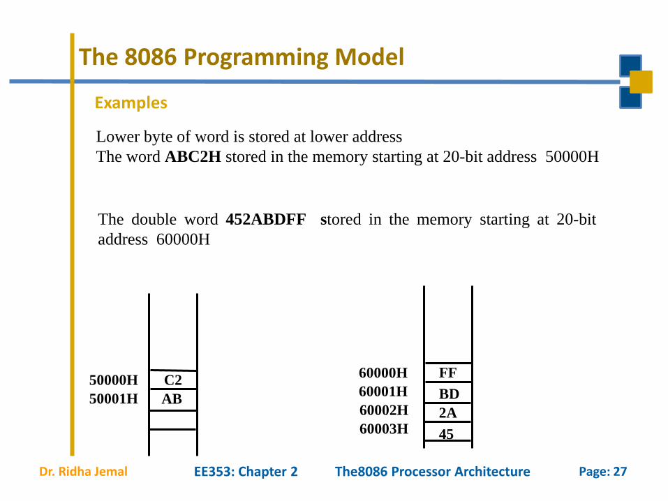
Examples
Lower byte of word is stored at lower address
The word ABC2H stored in the memory starting at 20-bit address 50000H
The double word 452ABDFF stored in the memory starting at 20-bit
address 60000H
C2
AB
50000H
50001H BD
FF
45
2A
60000H
60001H
60002H
60003H
Page: 28Dr. Ridha Jemal
Memory Addressing Mode:
EE353: Chapter 2 The8086 Processor Architecture
The 8086 Programming Model
Related Documents


![and...Draw and explain functional block diagram of the 8086 micro- processor. [8] Explain with a neat diagram of memory segmentation in the 8086 microprocessor. Or [81 Draw and explain](https://static.cupdf.com/doc/110x72/5e4eb30fd39dde0cf8262f40/and-draw-and-explain-functional-block-diagram-of-the-8086-micro-processor-8.jpg)