TFA9843J 2-channel audio amplifier (SE: 1 W to 20 W or BTL: 4 W to 40 W) Rev. 02 — 19 January 2004 Preliminary data 1. General description The TFA9843J contains two identical audio power amplifiers. The TFA9843J can be used as two Single-Ended (SE) channels with a fixed gain of 26 dB or one Bridge-Tied Load (BTL) channel with a fixed gain of 32 dB. The TFA9843J comes in a 9-pin DIL-bent-SIL (DBS7P) power package. The TFA9843J is pin compatible with the TFA9842J and TFA9841J. The TFA9843J contains a unique protection circuit that is solely based on multiple temperature measurements inside the chip. This gives maximum output power for all supply voltages and load conditions with no unnecessary audio holes. Almost any supply voltage and load impedance combination can be made as long as thermal boundary conditions (number of channels used, external heatsink and ambient temperature) allow it. 2. Features ■ SE: 1 W to 20 W; BTL: 4 W to 40 W operation possibility ■ Soft clipping ■ Standby and mute mode ■ No on/off switching plops ■ Low standby current ■ High supply voltage ripple rejection ■ Outputs short-circuit protected to ground, supply and across the load ■ Thermally protected ■ Pin compatible with the TFA9842J and TFA9841J. 3. Applications ■ Television ■ PC speakers ■ Boom box ■ Mini and micro audio receivers.

Welcome message from author
This document is posted to help you gain knowledge. Please leave a comment to let me know what you think about it! Share it to your friends and learn new things together.
Transcript
TFA9843J2-channel audio amplifier (SE: 1 W to 20 W or BTL: 4 W to40 W)Rev. 02 — 19 January 2004 Preliminary data
1. General description
The TFA9843J contains two identical audio power amplifiers. The TFA9843J can beused as two Single-Ended (SE) channels with a fixed gain of 26 dB or oneBridge-Tied Load (BTL) channel with a fixed gain of 32 dB.
The TFA9843J comes in a 9-pin DIL-bent-SIL (DBS7P) power package. TheTFA9843J is pin compatible with the TFA9842J and TFA9841J.
The TFA9843J contains a unique protection circuit that is solely based on multipletemperature measurements inside the chip. This gives maximum output power for allsupply voltages and load conditions with no unnecessary audio holes. Almost anysupply voltage and load impedance combination can be made as long as thermalboundary conditions (number of channels used, external heatsink and ambienttemperature) allow it.
2. Features
SE: 1 W to 20 W; BTL: 4 W to 40 W operation possibility
Soft clipping
Standby and mute mode
No on/off switching plops
Low standby current
High supply voltage ripple rejection
Outputs short-circuit protected to ground, supply and across the load
Thermally protected
Pin compatible with the TFA9842J and TFA9841J.
3. Applications
Television
PC speakers
Boom box
Mini and micro audio receivers.
Philips Semiconductors TFA9843J2-channel audio amplifier (2 x SE or 1 x BTL)
Preliminary data Rev. 02 — 19 January 2004 2 of 21
9397 750 12587 © Koninklijke Philips Electronics N.V. 2004. All rights reserved.
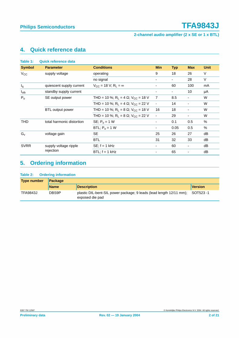
4. Quick reference data
5. Ordering information
Table 1: Quick reference data
Symbol Parameter Conditions Min Typ Max Unit
VCC supply voltage operating 9 18 26 V
no signal - - 28 V
Iq quiescent supply current VCC = 18 V; RL = ∞ - 60 100 mA
Istb standby supply current - - 10 µA
Po SE output power THD = 10 %; RL = 4 Ω; VCC = 18 V 7 8.5 - W
THD = 10 %; RL = 4 Ω; VCC = 22 V - 14 - W
BTL output power THD = 10 %; RL = 8 Ω; VCC = 18 V 16 18 - W
THD = 10 %; RL = 8 Ω; VCC = 22 V - 29 - W
THD total harmonic distortion SE; Po = 1 W - 0.1 0.5 %
BTL; Po = 1 W - 0.05 0.5 %
Gv voltage gain SE 25 26 27 dB
BTL 31 32 33 dB
SVRR supply voltage ripplerejection
SE; f = 1 kHz - 60 - dB
BTL; f = 1 kHz - 65 - dB
Table 2: Ordering information
Type number Package
Name Description Version
TFA9843J DBS9P plastic DIL-bent-SIL power package; 9 leads (lead length 12/11 mm);exposed die pad
SOT523 -1
Philips Semiconductors TFA9843J2-channel audio amplifier (2 x SE or 1 x BTL)
Preliminary data Rev. 02 — 19 January 2004 3 of 21
9397 750 12587 © Koninklijke Philips Electronics N.V. 2004. All rights reserved.
6. Block diagram
7. Pinning information
7.1 Pinning
Fig 1. Block diagram.
MDB023
60 kΩ
60 kΩ
STANDBYMUTE
ON
SHORT-CIRCUITAND
TEMPERATUREPROTECTION
VREF
0.5VCC
VCC
VCC
9
4IN1+
IN2+
OUT1+
OUT2−
SVR
CIV
MODE
1
3
7
8
2
6
5
GND
TFA9843J
Fig 2. Pin configuration.
TFA9843J
MDB024
IN2+
OUT2−
CIV
IN1+
GND
SVR
MODE
OUT1+VCC
2
1
3
4
5
6
7
8
9
Philips Semiconductors TFA9843J2-channel audio amplifier (2 x SE or 1 x BTL)
Preliminary data Rev. 02 — 19 January 2004 4 of 21
9397 750 12587 © Koninklijke Philips Electronics N.V. 2004. All rights reserved.
7.2 Pin description
8. Functional description
8.1 Input configurationThe input cut-off frequency is:
(1)
Single-ended application: Ri = 60 kΩ and Ci = 220 nF:
(2)
Bridge-tied load application: Ri = 30 kΩ and Ci = 470 nF:
(3)
As shown in Equation 2 and Equation 3, large capacitor values for the inputs are notnecessary; so the switch-on delay during charging of the input capacitors can beminimized. This results in a good low frequency response and good switch-onbehavior.
8.2 Power amplifierThe power amplifier is a Bridge-Tied Load (BTL) or Single-Ended (SE) amplifier withan all-NPN output stage, capable of delivering a peak output current of 4 A.
Using the TFA9843J as a BTL amplifier offers the following advantages:
• Lower peak value of the supply current
• Ripple frequency on the supply voltage is twice the signal frequency
Table 3: Pin description
Symbol Pin Description
IN2+ 1 input 2
OUT2− 2 inverted loudspeaker terminal 2
CIV 3 common input voltage decoupling
IN1+ 4 input 1
GND 5 ground
SVR 6 half supply voltage decoupling (ripple rejection)
MODE 7 mode selection input (standby, mute and operating)
OUT1+ 8 non inverted loudspeaker terminal 1
VCC 9 supply voltage
f i cut off–( )1
2π Ri Ci×( )-----------------------------=
f i cut off–( )1
2π 60 103× 220× 10
9–×( )----------------------------------------------------------------- 12 Hz= =
f i cut off–( )1
2π 30 103× 470× 10
9–×( )----------------------------------------------------------------- 11 Hz= =
Philips Semiconductors TFA9843J2-channel audio amplifier (2 x SE or 1 x BTL)
Preliminary data Rev. 02 — 19 January 2004 5 of 21
9397 750 12587 © Koninklijke Philips Electronics N.V. 2004. All rights reserved.
• No expensive DC-blocking capacitor
• Good low frequency performance.
8.2.1 Output power measurement
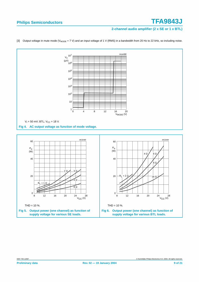
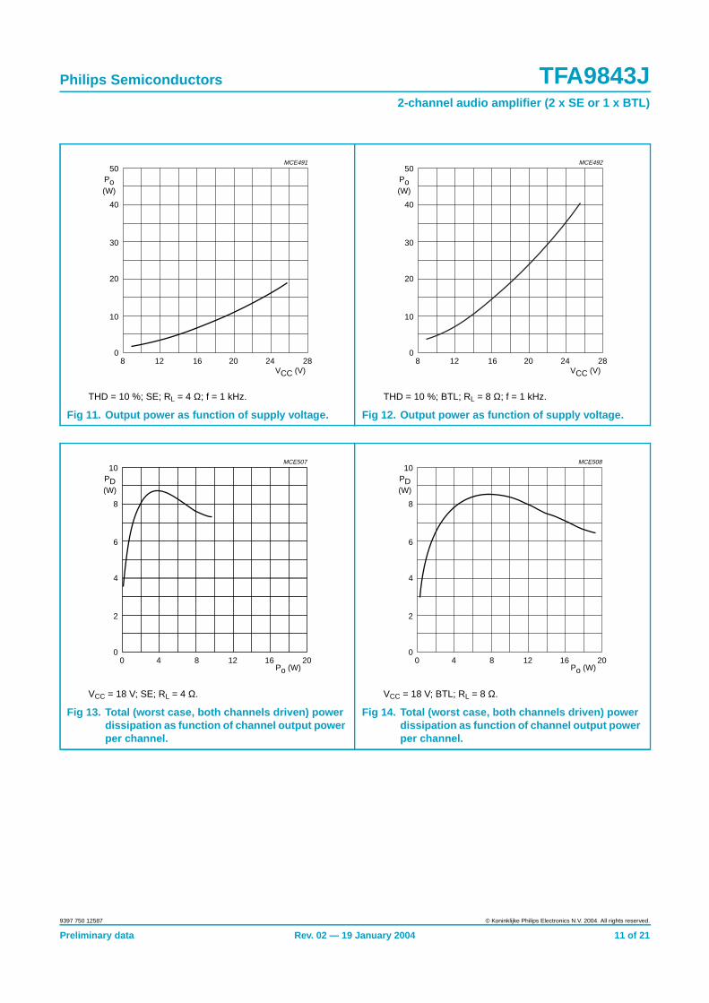
The output power as a function of the supply voltage is measured on the output pinsat THD = 10 %; see Figure 11. The maximum output power is limited by the supplyvoltage of 26 V and the maximum available output current is 4 A repetitive peakcurrent. A minimum load (SE) of 3 Ω is required for supply voltages > 22 V; seeFigure 5. A minimum load (BTL) of 6 Ω is required for supply voltages > 22 V; seeFigure 6.
8.2.2 Headroom
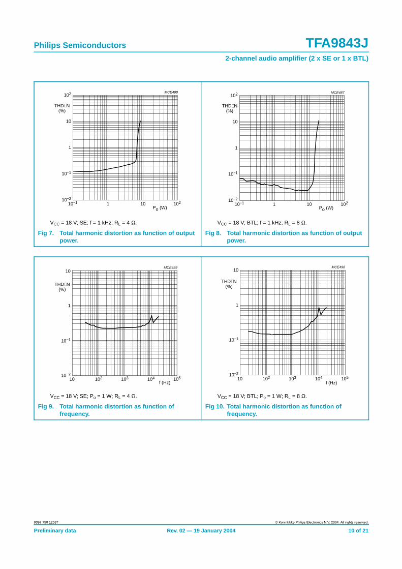
Typical CD music requires at least 12 dB (factor 15.85) dynamic headroom,compared to the average power output, for transferring the loudest parts withoutdistortion. At VCC = 18 V and Po = 5 W (SE with RL = 4 Ω) or Po = 10 W (BTL withRL = 8 Ω) at THD = 0.2 % (see Figure 7), the Average Listening Level (ALL) musicpower without any distortion yields:
(4)
(5)
The power dissipation can be derived from Figure 13 (SE) or Figure 14 (BTL) for 0 dBrespectively 12 dB headroom (see Table 4).
For the average listening level a power dissipation of 4.2 W can be used for aheatsink calculation.
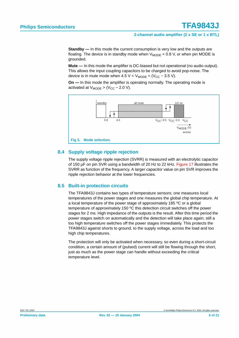
8.3 Mode selectionThe TFA9843J has three functional modes, which can be selected by applying theproper DC voltage to pin MODE (see Table 5 and Figure 3).
Table 4: Power rating as function of headroom
Headroom Power output (THD = 0.2 %) Power dissipation (P D);both channels drivenSE BTL
0 dB Po = 5 W Po = 10 W 8.4 W
12 dB Po(ALL) = 315 mW Po(ALL) = 630 mW 4.2 W
Po ALL SE,( )5 10
3×15.85
----------------- 315 mW= =
Po ALL BTL,( )10 10
3×15.85
-------------------- 630 mW= =
Table 5: Mode selection
VMODE Amplifiers 1 and 2
0 to 0.8 V standby
4.5 V to (VCC − 3.5 V) mute
(VCC − 2.0 V) to VCC on
Philips Semiconductors TFA9843J2-channel audio amplifier (2 x SE or 1 x BTL)
Preliminary data Rev. 02 — 19 January 2004 6 of 21
9397 750 12587 © Koninklijke Philips Electronics N.V. 2004. All rights reserved.
Standby — In this mode the current consumption is very low and the outputs arefloating. The device is in standby mode when VMODE < 0.8 V, or when pin MODE isgrounded.
Mute — In this mode the amplifier is DC-biased but not operational (no audio output).This allows the input coupling capacitors to be charged to avoid pop-noise. Thedevice is in mute mode when 4.5 V < VMODE < (VCC − 3.5 V).
On — In this mode the amplifier is operating normally. The operating mode isactivated at VMODE > (VCC − 2.0 V).
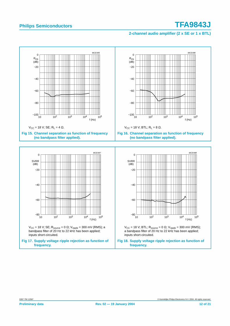
8.4 Supply voltage ripple rejectionThe supply voltage ripple rejection (SVRR) is measured with an electrolytic capacitorof 150 µF on pin SVR using a bandwidth of 20 Hz to 22 kHz. Figure 17 illustrates theSVRR as function of the frequency. A larger capacitor value on pin SVR improves theripple rejection behavior at the lower frequencies.
8.5 Built-in protection circuitsThe TFA9843J contains two types of temperature sensors; one measures localtemperatures of the power stages and one measures the global chip temperature. Ata local temperature of the power stage of approximately 185 oC or a globaltemperature of approximately 150 oC this detection circuit switches off the powerstages for 2 ms. High impedance of the outputs is the result. After this time period thepower stages switch on automatically and the detection will take place again; still atoo high temperature switches off the power stages immediately. This protects theTFA9843J against shorts to ground, to the supply voltage, across the load and toohigh chip temperatures.
The protection will only be activated when necessary, so even during a short-circuitcondition, a certain amount of (pulsed) current will still be flowing through the short,just as much as the power stage can handle without exceeding the criticaltemperature level.
Fig 3. Mode selection.
MCE502
standby all mute 1/2 on
0.8 4.5 VCC−3.5 VCC
VMODE (V)
VCC−2.0
Philips Semiconductors TFA9843J2-channel audio amplifier (2 x SE or 1 x BTL)
Preliminary data Rev. 02 — 19 January 2004 7 of 21
9397 750 12587 © Koninklijke Philips Electronics N.V. 2004. All rights reserved.
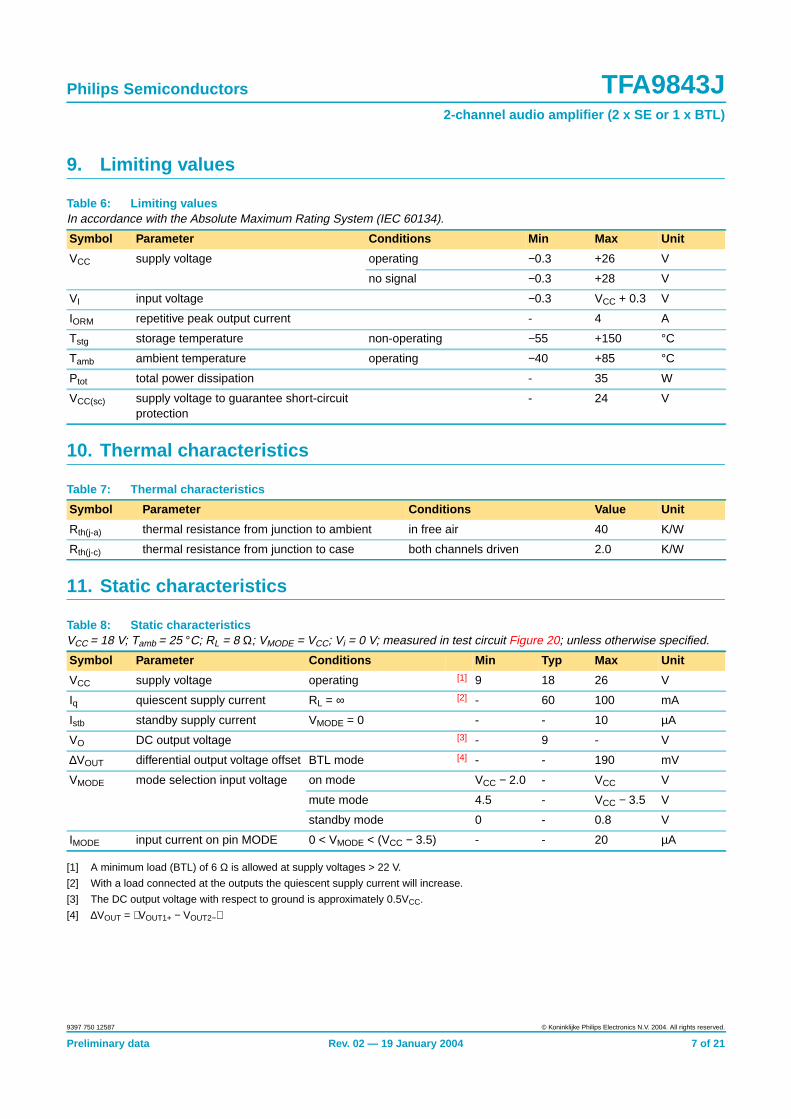
9. Limiting values
10. Thermal characteristics
11. Static characteristics
[1] A minimum load (BTL) of 6 Ω is allowed at supply voltages > 22 V.
[2] With a load connected at the outputs the quiescent supply current will increase.
[3] The DC output voltage with respect to ground is approximately 0.5VCC.
[4] ∆VOUT = VOUT1+ − VOUT2−
Table 6: Limiting valuesIn accordance with the Absolute Maximum Rating System (IEC 60134).
Symbol Parameter Conditions Min Max Unit
VCC supply voltage operating −0.3 +26 V
no signal −0.3 +28 V
VI input voltage −0.3 VCC + 0.3 V
IORM repetitive peak output current - 4 A
Tstg storage temperature non-operating −55 +150 °C
Tamb ambient temperature operating −40 +85 °C
Ptot total power dissipation - 35 W
VCC(sc) supply voltage to guarantee short-circuitprotection
- 24 V
Table 7: Thermal characteristics
Symbol Parameter Conditions Value Unit
Rth(j-a) thermal resistance from junction to ambient in free air 40 K/W
Rth(j-c) thermal resistance from junction to case both channels driven 2.0 K/W
Table 8: Static characteristicsVCC = 18 V; Tamb = 25 °C; RL = 8 Ω; VMODE = VCC; Vi = 0 V; measured in test circuit Figure 20; unless otherwise specified.
Symbol Parameter Conditions Min Typ Max Unit
VCC supply voltage operating [1] 9 18 26 V
Iq quiescent supply current RL = ∞ [2] - 60 100 mA
Istb standby supply current VMODE = 0 - - 10 µA
VO DC output voltage [3] - 9 - V
∆VOUT differential output voltage offset BTL mode [4] - - 190 mV
VMODE mode selection input voltage on mode VCC − 2.0 - VCC V
mute mode 4.5 - VCC − 3.5 V
standby mode 0 - 0.8 V
IMODE input current on pin MODE 0 < VMODE < (VCC − 3.5) - - 20 µA
Philips Semiconductors TFA9843J2-channel audio amplifier (2 x SE or 1 x BTL)
Preliminary data Rev. 02 — 19 January 2004 8 of 21
9397 750 12587 © Koninklijke Philips Electronics N.V. 2004. All rights reserved.
12. Dynamic characteristics
[1] The noise output voltage is measured at the output in a frequency range from 20 Hz to 22 kHz (unweighted), with a source impedanceRsource = 0 Ω at the input.
[2] Supply voltage ripple rejection is measured at the output, with a source impedance Rsource = 0 Ω at the input and with a frequency rangefrom 20 Hz to 22 kHz (unweighted). The ripple voltage is a sine wave with a frequency fripple and an amplitude of 300 mV (RMS), whichis applied to the positive supply rail.
[3] Output voltage in mute mode (VMODE = 7 V) and an input voltage of 1 V (RMS) in a bandwidth from 20 Hz to 22 kHz, so including noise.
[1] The noise output voltage is measured at the output in a frequency range from 20 Hz to 22 kHz (unweighted), with a source impedanceRsource = 0 Ω at the input.
[2] Supply voltage ripple rejection is measured at the output, with a source impedance Rsource = 0 Ω at the input and with a frequency rangefrom 20 Hz to 22 kHz (unweighted). The ripple voltage is a sine wave with a frequency fripple and an amplitude of 300 mV (RMS), whichis applied to the positive supply rail.
Table 9: Dynamic characteristics SEVCC = 18 V; Tamb = 25 °C; RL = 4 Ω; f = 1 kHz; VMODE = VCC; measured in test circuit Figure 19; unless otherwise specified.
Symbol Parameter Conditions Min Typ Max Unit
Po output power THD = 10 %; RL = 4 Ω 7 8.5 - W
THD = 0.5 % RL = 4 Ω - 6.5 - W
VCC = 22 V;THD = 10 %; RL = 4 Ω
- 14 - W
THD total harmonic distortion Po = 1 W - 0.1 0.5 %
Gv SE voltage gain 25 26 27 dB
Zi input impedance 40 60 - kΩ
Vn(o) noise output voltage [1] - 150 - µV
SVRR supply voltage ripplerejection
fripple = 1 kHz [2] - 60 - dB
fripple = 100 Hz to 20 kHz [2] - 60 - dB
Vo(mute) output voltage in mute mode [3] - - 150 µV
αcs channel separation Rsource = 0 Ω 50 60 - dB
|Gv| channel unbalance - - 1 dB
Table 10: Dynamic characteristics BTLVCC = 18 V; Tamb = 25 °C; RL = 8 Ω; f = 1 kHz; VMODE = VCC; measured in test circuit Figure 20; unless otherwise specified.
Symbol Parameter Conditions Min Typ Max Unit
Po output power THD = 10 %; RL = 8 Ω 16 18 - W
THD = 0.5 %; RL = 8 Ω - 14 W
VCC = 22 V;THD = 10 %; RL = 8 Ω
- 29 - W
THD total harmonic distortion Po = 1 W - 0.05 0.5 %
Gv BTL voltage gain 31 32 33 dB
Zi input impedance 20 30 - kΩ
Vn(o) noise output voltage [1] - 200 - µV
SVRR supply voltage ripplerejection
fripple = 1 kHz [2] - 65 - dB
fripple = 100 Hz to 20 kHz [2] - 65 - dB
Vo(mute) output voltage in mute mode [3] - - 250 µV
αcs channel separation Rsource = 0 Ω 50 65 - dB
|Gv| channel unbalance - - 1 dB
Philips Semiconductors TFA9843J2-channel audio amplifier (2 x SE or 1 x BTL)
Preliminary data Rev. 02 — 19 January 2004 9 of 21
9397 750 12587 © Koninklijke Philips Electronics N.V. 2004. All rights reserved.
[3] Output voltage in mute mode (VMODE = 7 V) and an input voltage of 1 V (RMS) in a bandwidth from 20 Hz to 22 kHz, so including noise.
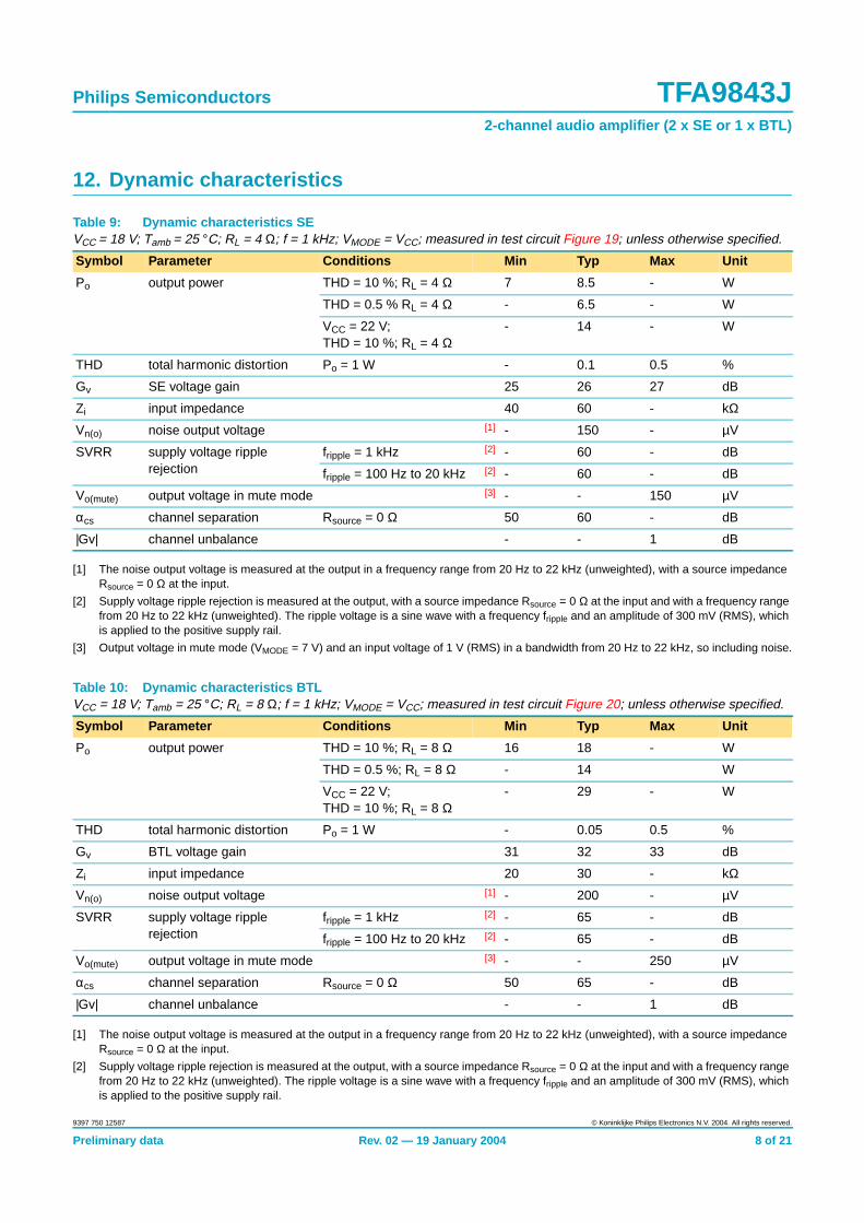
Vi = 50 mV; BTL; VCC = 18 V.
Fig 4. AC output voltage as function of mode voltage.
20VMODE (V)
0 4 8 12
Vo(µV)
16
107
106
105
104
103
102
10
1
mce486
THD = 10 %. THD = 10 %.
Fig 5. Output power (one channel) as function ofsupply voltage for various SE loads.
Fig 6. Output power (one channel) as function ofsupply voltage for various BTL loads.
8
40
60
20
012 28
VCC (V)16 20
Po(W)
24
MCE485
RL = 1 Ω
8 Ω
4 Ω
3 Ω2 Ω
8
60
40
20
012 28
VCC (V)16 20
Po(W)
24
MCE484
RL = 2 Ω 16 Ω
8 Ω
6 Ω4 Ω
Philips Semiconductors TFA9843J2-channel audio amplifier (2 x SE or 1 x BTL)
Preliminary data Rev. 02 — 19 January 2004 10 of 21
9397 750 12587 © Koninklijke Philips Electronics N.V. 2004. All rights reserved.
VCC = 18 V; SE; f = 1 kHz; RL = 4 Ω. VCC = 18 V; BTL; f = 1 kHz; RL = 8 Ω.
Fig 7. Total harmonic distortion as function of outputpower.
Fig 8. Total harmonic distortion as function of outputpower.
102
10
1
10−1
10−2
MCE488
10−1 1021 10Po (W)
THD+N(%)
102
10
1
10−1
10−2
MCE487
10−1 1
THD+N(%)
10Po (W)
102
VCC = 18 V; SE; Po = 1 W; RL = 4 Ω. VCC = 18 V; BTL; Po = 1 W; RL = 8 Ω.
Fig 9. Total harmonic distortion as function offrequency.
Fig 10. Total harmonic distortion as function offrequency.
10
1
10−1
10−2
MCE489
10
THD+N(%)
f (Hz)102 103 104 105
10
1
10−1
10−2
MCE490
10
THD+N(%)
f (Hz)102 103 104 105
Philips Semiconductors TFA9843J2-channel audio amplifier (2 x SE or 1 x BTL)
Preliminary data Rev. 02 — 19 January 2004 11 of 21
9397 750 12587 © Koninklijke Philips Electronics N.V. 2004. All rights reserved.
THD = 10 %; SE; RL = 4 Ω; f = 1 kHz. THD = 10 %; BTL; RL = 8 Ω; f = 1 kHz.
Fig 11. Output power as function of supply voltage. Fig 12. Output power as function of supply voltage.
8 28
50
0
10
20
30
40
12
Po(W)
16 20 24VCC (V)
MCE491
8 28
50
0
10
20
30
40
12
Po(W)
16 20 24VCC (V)
MCE492
VCC = 18 V; SE; RL = 4 Ω. VCC = 18 V; BTL; RL = 8 Ω.
Fig 13. Total (worst case, both channels driven) powerdissipation as function of channel output powerper channel.
Fig 14. Total (worst case, both channels driven) powerdissipation as function of channel output powerper channel.
0 20Po (W)
10
0
2
4
6
8
4
PD(W)
8 12 16
MCE507
0 20Po (W)
10
0
2
4
6
8
4
PD(W)
8 12 16
MCE508
Philips Semiconductors TFA9843J2-channel audio amplifier (2 x SE or 1 x BTL)
Preliminary data Rev. 02 — 19 January 2004 12 of 21
9397 750 12587 © Koninklijke Philips Electronics N.V. 2004. All rights reserved.
VCC = 18 V; SE; RL = 4 Ω. VCC = 18 V; BTL; RL = 8 Ω.
Fig 15. Channel separation as function of frequency(no bandpass filter applied).
Fig 16. Channel separation as function of frequency(no bandpass filter applied).
−100
0
−80
−60
−40
−20
MCE495
10
αcs(dB)
f (Hz)102 103 104 105
−100
0
−80
−60
−40
−20
MCE496
10
αcs(dB)
f (Hz)102 103 104 105
VCC = 18 V; SE; Rsource = 0 Ω; Vripple = 300 mV (RMS); abandpass filter of 20 Hz to 22 kHz has been applied;inputs short-circuited.
VCC = 18 V; BTL; Rsource = 0 Ω; Vripple = 300 mV (RMS);a bandpass filter of 20 Hz to 22 kHz has been applied;inputs short-circuited.
Fig 17. Supply voltage ripple rejection as function offrequency.
Fig 18. Supply voltage ripple rejection as function offrequency.
−80
−60
−40
−20
0MCE497
10
SVRR(dB)
f (Hz)102 103 104 105
−80
−60
−40
−20
0MCE498
10
SVRR(dB)
f (Hz)102 103 104 105
Philips Semiconductors TFA9843J2-channel audio amplifier (2 x SE or 1 x BTL)
Preliminary data Rev. 02 — 19 January 2004 13 of 21
9397 750 12587 © Koninklijke Philips Electronics N.V. 2004. All rights reserved.
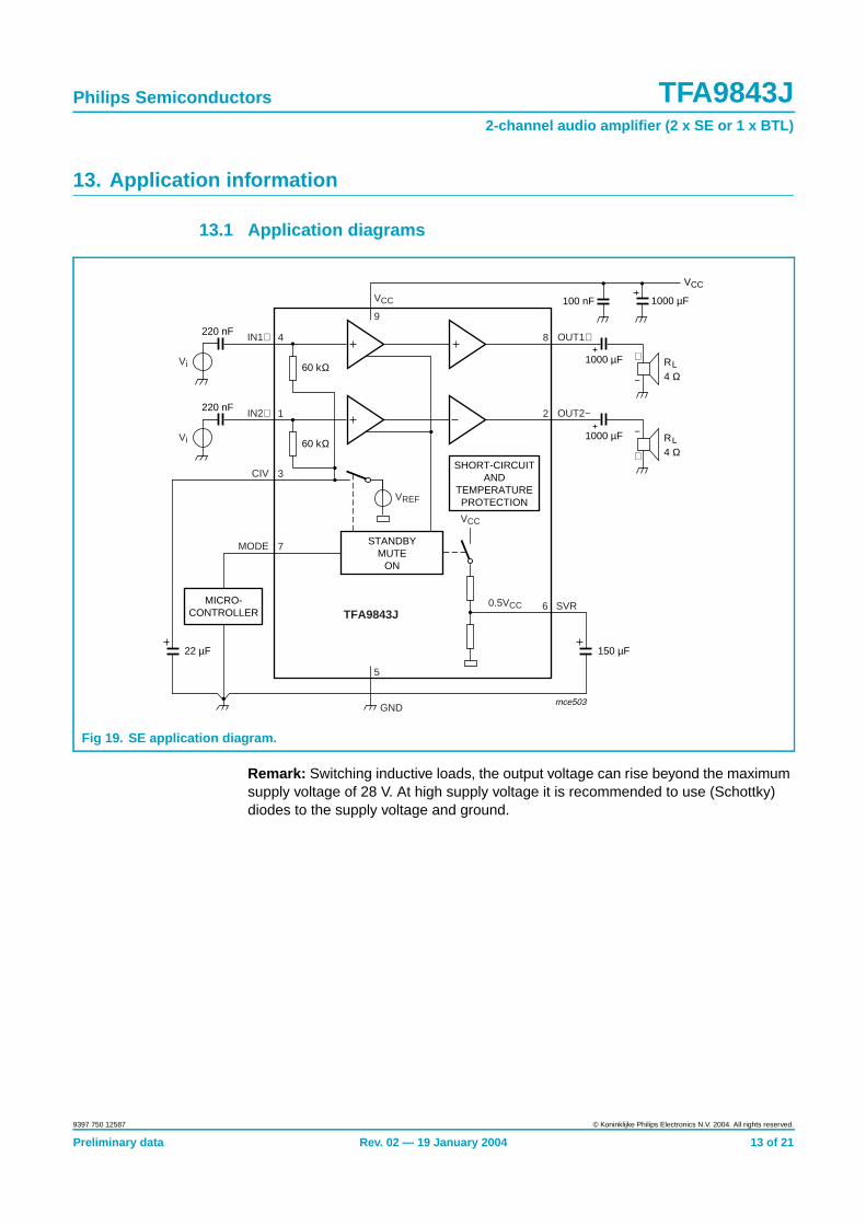
13. Application information
13.1 Application diagrams
Remark: Switching inductive loads, the output voltage can rise beyond the maximumsupply voltage of 28 V. At high supply voltage it is recommended to use (Schottky)diodes to the supply voltage and ground.
Fig 19. SE application diagram.
MICRO-CONTROLLER
mce503
60 kΩ
60 kΩ
22 µF
220 nF
150 µF
STANDBYMUTE
ON
SHORT-CIRCUITAND
TEMPERATUREPROTECTIONVREF
0.5VCC
VCC
VCC
9
4IN1+
IN2+
OUT1+
OUT2−
SVR
CIV
MODE
1
3
7
8
2
6
5
GND
TFA9843J
Vi
220 nF
Vi
VCC
1000 µF
1000 µF
1000 µF
100 nF
+
−
RL4 Ω
RL4 Ω
+
−
Philips Semiconductors TFA9843J2-channel audio amplifier (2 x SE or 1 x BTL)
Preliminary data Rev. 02 — 19 January 2004 14 of 21
9397 750 12587 © Koninklijke Philips Electronics N.V. 2004. All rights reserved.
Remark: Switching inductive loads, the output voltage can rise beyond the maximumsupply voltage of 28 V. At high supply voltage it is recommended to use (Schottky)diodes to the supply voltage and ground.
13.2 Printed-circuit board
13.2.1 Layout and grounding
To obtain a high-level system performance, certain grounding techniques areessential. The input reference grounds have to be tied with their respective sourcegrounds and must have separate tracks from the power ground tracks; this willprevent the large (output) signal currents from interfering with the small AC inputsignals. The small-signal ground tracks should be physically located as far aspossible from the power ground tracks. Supply and output tracks should be as wideas possible for delivering maximum output power.
Fig 20. BTL application diagram.
MICRO-CONTROLLER
MDB026
60 kΩ
60 kΩ
22 µF
470 nF
150 µF
STANDBYMUTE
ON
SHORT-CIRCUITAND
TEMPERATUREPROTECTIONVREF
0.5VCC
VCC
VCC
9
4IN1+
IN2+
OUT1+
OUT2−
SVR
CIV
MODE
1
3
7
8
2
6
5
GND
TFA9843J
Vi
VCC
1000 µF100 nF
RL8 Ω
+
−
Philips Semiconductors TFA9843J2-channel audio amplifier (2 x SE or 1 x BTL)
Preliminary data Rev. 02 — 19 January 2004 15 of 21
9397 750 12587 © Koninklijke Philips Electronics N.V. 2004. All rights reserved.
13.2.2 Power supply decoupling
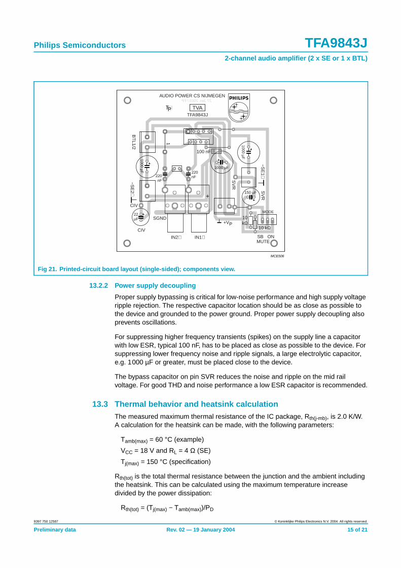
Proper supply bypassing is critical for low-noise performance and high supply voltageripple rejection. The respective capacitor location should be as close as possible tothe device and grounded to the power ground. Proper power supply decoupling alsoprevents oscillations.
For suppressing higher frequency transients (spikes) on the supply line a capacitorwith low ESR, typical 100 nF, has to be placed as close as possible to the device. Forsuppressing lower frequency noise and ripple signals, a large electrolytic capacitor,e.g. 1000 µF or greater, must be placed close to the device.
The bypass capacitor on pin SVR reduces the noise and ripple on the mid railvoltage. For good THD and noise performance a low ESR capacitor is recommended.
13.3 Thermal behavior and heatsink calculationThe measured maximum thermal resistance of the IC package, Rth(j-mb), is 2.0 K/W.A calculation for the heatsink can be made, with the following parameters:
Tamb(max) = 60 °C (example)
VCC = 18 V and RL = 4 Ω (SE)
Tj(max) = 150 °C (specification)
Rth(tot) is the total thermal resistance between the junction and the ambient includingthe heatsink. This can be calculated using the maximum temperature increasedivided by the power dissipation:
Rth(tot) = (Tj(max) − Tamb(max))/PD
Fig 21. Printed-circuit board layout (single-sided); components view.
AUDIO POWER CS NIJMEGEN27 Jan. 2003 / FP
IN2+ IN1+MUTESB ON
TVATFA9843J
−SE
2+
−SE
1+
+VP
1000 µF1000 µF 1000 µF
BT
L1/2
1
22µF
10 kΩ
10kΩ
MCE506
100 nF
150 µF
220nF220
nF
MODE
SGND
SV
R
SV
R
CIV
CIV
Philips Semiconductors TFA9843J2-channel audio amplifier (2 x SE or 1 x BTL)
Preliminary data Rev. 02 — 19 January 2004 16 of 21
9397 750 12587 © Koninklijke Philips Electronics N.V. 2004. All rights reserved.
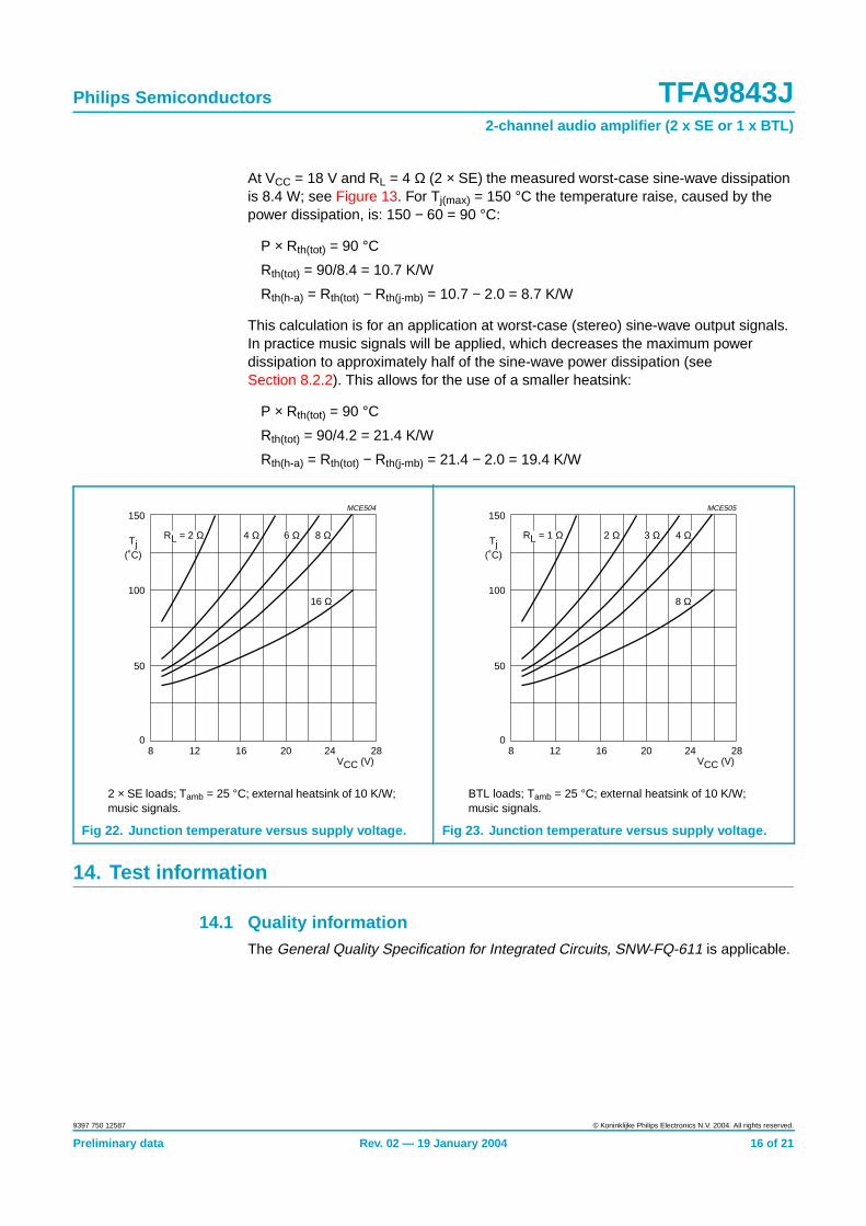
At VCC = 18 V and RL = 4 Ω (2 × SE) the measured worst-case sine-wave dissipationis 8.4 W; see Figure 13. For Tj(max) = 150 °C the temperature raise, caused by thepower dissipation, is: 150 − 60 = 90 °C:
P × Rth(tot) = 90 °C
Rth(tot) = 90/8.4 = 10.7 K/W
Rth(h-a) = Rth(tot) − Rth(j-mb) = 10.7 − 2.0 = 8.7 K/W
This calculation is for an application at worst-case (stereo) sine-wave output signals.In practice music signals will be applied, which decreases the maximum powerdissipation to approximately half of the sine-wave power dissipation (seeSection 8.2.2). This allows for the use of a smaller heatsink:
P × Rth(tot) = 90 °C
Rth(tot) = 90/4.2 = 21.4 K/W
Rth(h-a) = Rth(tot) − Rth(j-mb) = 21.4 − 2.0 = 19.4 K/W
14. Test information
14.1 Quality informationThe General Quality Specification for Integrated Circuits, SNW-FQ-611 is applicable.
2 × SE loads; Tamb = 25 °C; external heatsink of 10 K/W;music signals.
BTL loads; Tamb = 25 °C; external heatsink of 10 K/W;music signals.
Fig 22. Junction temperature versus supply voltage. Fig 23. Junction temperature versus supply voltage.
8
150
100
50
012 28
VCC (V)16 20 24
MCE504
Tj(˚C)
RL = 2 Ω 4 Ω 6 Ω 8 Ω
16 Ω
8
150
100
50
012 28
VCC (V)16 20 24
MCE505
Tj(˚C)
2 Ω 3 Ω 4 Ω
8 Ω
RL = 1 Ω
Philips Semiconductors TFA9843J2-channel audio amplifier (2 x SE or 1 x BTL)
Preliminary data Rev. 02 — 19 January 2004 17 of 21
9397 750 12587 © Koninklijke Philips Electronics N.V. 2004. All rights reserved.
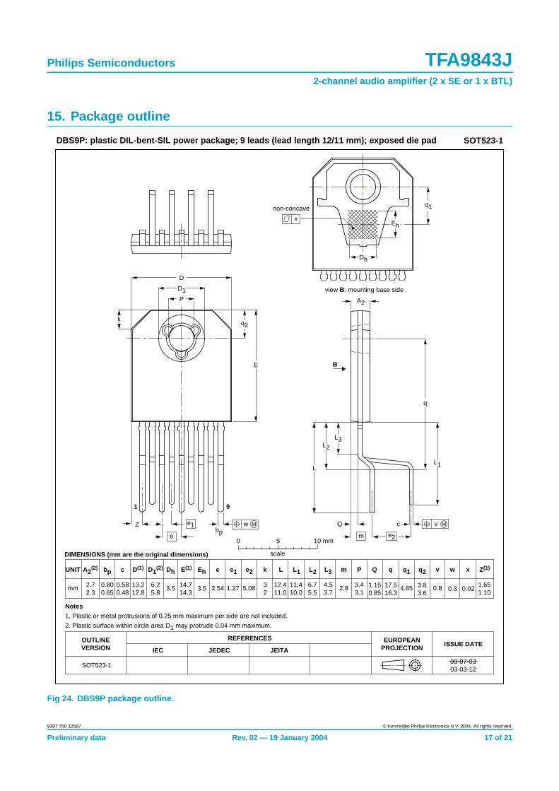
15. Package outline
Fig 24. DBS9P package outline.
REFERENCESOUTLINEVERSION
EUROPEANPROJECTION ISSUE DATE
IEC JEDEC JEITA
DIMENSIONS (mm are the original dimensions)
Notes
1. Plastic or metal protrusions of 0.25 mm maximum per side are not included.
2. Plastic surface within circle area D1 may protrude 0.04 mm maximum.
SOT523-1
0 10 mm5
scale
w Mbp
Dh
q1
Z
1 9
e
e1
m e2
x
A2
non-concave
D1
D
P
kq2
L3L2
L
Q c
E
00-07-0303-03-12
DBS9P: plastic DIL-bent-SIL power package; 9 leads (lead length 12/11 mm); exposed die pad SOT523-1
view B: mounting base side
B
UNIT bp L1c D(1) Dh L q2
mm 2.72.3
A2(2)
0.800.65
0.580.48
13.212.8
D1(2)
6.25.8
3.5
Eh
3.5
e
2.54
e1
1.27
e2
5.08 4.85
QE(1)
14.714.3
Z(1)
1.651.10
11.410.0
L2
6.75.5
L3
4.53.7
3.43.1
1.150.85
q
17.516.3
q1
2.8
m
0.8
v
3.83.6
32
12.411.0
Pk
0.02
x
0.3
w
Eh
L1
q
v M
Philips Semiconductors TFA9843J2-channel audio amplifier (2 x SE or 1 x BTL)
Preliminary data Rev. 02 — 19 January 2004 18 of 21
9397 750 12587 © Koninklijke Philips Electronics N.V. 2004. All rights reserved.
16. Soldering
16.1 Introduction to soldering through-hole mount packagesThis text gives a brief insight to wave, dip and manual soldering. A more in-depthaccount of soldering ICs can be found in our Data Handbook IC26; Integrated CircuitPackages (document order number 9398 652 90011).
Wave soldering is the preferred method for mounting of through-hole mount ICpackages on a printed-circuit board.
16.2 Soldering by dipping or by solder waveDriven by legislation and environmental forces the worldwide use of lead-free solderpastes is increasing. Typical dwell time of the leads in the wave ranges from3 to 4 seconds at 250 °C or 265 °C, depending on solder material applied, SnPb orPb-free respectively.
The total contact time of successive solder waves must not exceed 5 seconds.
The device may be mounted up to the seating plane, but the temperature of theplastic body must not exceed the specified maximum storage temperature (Tstg(max)).If the printed-circuit board has been pre-heated, forced cooling may be necessaryimmediately after soldering to keep the temperature within the permissible limit.
16.3 Manual solderingApply the soldering iron (24 V or less) to the lead(s) of the package, either below theseating plane or not more than 2 mm above it. If the temperature of the soldering ironbit is less than 300 °C it may remain in contact for up to 10 seconds. If the bittemperature is between 300 and 400 °C, contact may be up to 5 seconds.
16.4 Package related soldering information
[1] For SDIP packages, the longitudinal axis must be parallel to the transport direction of theprinted-circuit board.
[2] For PMFP packages hot bar soldering or manual soldering is suitable.
Table 11: Suitability of through-hole mount IC packages for dipping and wavesoldering methods
Package Soldering method
Dipping Wave
DBS, DIP, HDIP, RDBS, SDIP, SIL suitable suitable[1]
PMFP[2] − not suitable
Philips Semiconductors TFA9843J2-channel audio amplifier (2 x SE or 1 x BTL)
Preliminary data Rev. 02 — 19 January 2004 19 of 21
9397 750 12587 © Koninklijke Philips Electronics N.V. 2004. All rights reserved.
17. Revision history
Table 12: Revision history
Rev Date CPCN Description
02 20040119 - Preliminary data (9397 750 12587)
Modifications:
• Minor editorial changes.
01 20030915 - Preliminary data (9397 750 10777)
9397 750 12587
Philips Semiconductors TFA9843J2-channel audio amplifier (2 x SE or 1 x BTL)
© Koninklijke Philips Electronics N.V. 2004. All rights reserved.
Preliminary data Rev. 02 — 19 January 2004 20 of 21
Contact informationFor additional information, please visit http://www.semiconductors.philips.com .For sales office addresses, send e-mail to: [email protected] . Fax: +31 40 27 24825
18. Data sheet status
[1] Please consult the most recently issued data sheet before initiating or completing a design.
[2] The product status of the device(s) described in this data sheet may have changed since this data sheet was published. The latest information is available on the Internet atURL http://www.semiconductors.philips.com.
[3] For data sheets describing multiple type numbers, the highest-level product status determines the data sheet status.
19. Definitions
Short-form specification — The data in a short-form specification isextracted from a full data sheet with the same type number and title. Fordetailed information see the relevant data sheet or data handbook.
Limiting values definition — Limiting values given are in accordance withthe Absolute Maximum Rating System (IEC 60134). Stress above one ormore of the limiting values may cause permanent damage to the device.These are stress ratings only and operation of the device at these or at anyother conditions above those given in the Characteristics sections of thespecification is not implied. Exposure to limiting values for extended periodsmay affect device reliability.
Application information — Applications that are described herein for anyof these products are for illustrative purposes only. Philips Semiconductorsmake no representation or warranty that such applications will be suitable forthe specified use without further testing or modification.
20. Disclaimers
Life support — These products are not designed for use in life supportappliances, devices, or systems where malfunction of these products canreasonably be expected to result in personal injury. Philips Semiconductorscustomers using or selling these products for use in such applications do soat their own risk and agree to fully indemnify Philips Semiconductors for anydamages resulting from such application.
Right to make changes — Philips Semiconductors reserves the right tomake changes in the products - including circuits, standard cells, and/orsoftware - described or contained herein in order to improve design and/orperformance. When the product is in full production (status ‘Production’),relevant changes will be communicated via a Customer Product/ProcessChange Notification (CPCN). Philips Semiconductors assumes noresponsibility or liability for the use of any of these products, conveys nolicence or title under any patent, copyright, or mask work right to theseproducts, and makes no representations or warranties that these products arefree from patent, copyright, or mask work right infringement, unless otherwisespecified.
Level Data sheet status [1] Product status [2][3] Definition
I Objective data Development This data sheet contains data from the objective specification for product development. PhilipsSemiconductors reserves the right to change the specification in any manner without notice.
II Preliminary data Qualification This data sheet contains data from the preliminary specification. Supplementary data will be publishedat a later date. Philips Semiconductors reserves the right to change the specification without notice, inorder to improve the design and supply the best possible product.
III Product data Production This data sheet contains data from the product specification. Philips Semiconductors reserves theright to make changes at any time in order to improve the design, manufacturing and supply. Relevantchanges will be communicated via a Customer Product/Process Change Notification (CPCN).
© Koninklijke Philips Electronics N.V. 2004.Printed in The Netherlands
All rights are reserved. Reproduction in whole or in part is prohibited without the priorwritten consent of the copyright owner.
The information presented in this document does not form part of any quotation orcontract, is believed to be accurate and reliable and may be changed without notice. Noliability will be accepted by the publisher for any consequence of its use. Publicationthereof does not convey nor imply any license under patent- or other industrial orintellectual property rights.
Date of release: 19 January 2004 Document order number: 9397 750 12587
Contents
Philips Semiconductors TFA9843J2-channel audio amplifier (2 x SE or 1 x BTL)
1 General description . . . . . . . . . . . . . . . . . . . . . . 12 Features . . . . . . . . . . . . . . . . . . . . . . . . . . . . . . . 13 Applications . . . . . . . . . . . . . . . . . . . . . . . . . . . . 14 Quick reference data . . . . . . . . . . . . . . . . . . . . . 25 Ordering information . . . . . . . . . . . . . . . . . . . . . 26 Block diagram . . . . . . . . . . . . . . . . . . . . . . . . . . 37 Pinning information . . . . . . . . . . . . . . . . . . . . . . 37.1 Pinning . . . . . . . . . . . . . . . . . . . . . . . . . . . . . . . 37.2 Pin description . . . . . . . . . . . . . . . . . . . . . . . . . 48 Functional description . . . . . . . . . . . . . . . . . . . 48.1 Input configuration . . . . . . . . . . . . . . . . . . . . . . 48.2 Power amplifier . . . . . . . . . . . . . . . . . . . . . . . . . 48.2.1 Output power measurement . . . . . . . . . . . . . . . 58.2.2 Headroom. . . . . . . . . . . . . . . . . . . . . . . . . . . . . 58.3 Mode selection . . . . . . . . . . . . . . . . . . . . . . . . . 58.4 Supply voltage ripple rejection . . . . . . . . . . . . . 68.5 Built-in protection circuits . . . . . . . . . . . . . . . . . 69 Limiting values. . . . . . . . . . . . . . . . . . . . . . . . . . 710 Thermal characteristics. . . . . . . . . . . . . . . . . . . 711 Static characteristics. . . . . . . . . . . . . . . . . . . . . 712 Dynamic characteristics . . . . . . . . . . . . . . . . . . 813 Application information. . . . . . . . . . . . . . . . . . 1313.1 Application diagrams . . . . . . . . . . . . . . . . . . . 1313.2 Printed-circuit board . . . . . . . . . . . . . . . . . . . . 1413.2.1 Layout and grounding . . . . . . . . . . . . . . . . . . . 1413.2.2 Power supply decoupling . . . . . . . . . . . . . . . . 1513.3 Thermal behavior and heatsink calculation . . 1514 Test information . . . . . . . . . . . . . . . . . . . . . . . . 1614.1 Quality information . . . . . . . . . . . . . . . . . . . . . 1615 Package outline . . . . . . . . . . . . . . . . . . . . . . . . 1716 Soldering . . . . . . . . . . . . . . . . . . . . . . . . . . . . . 1816.1 Introduction to soldering through-hole
mount packages . . . . . . . . . . . . . . . . . . . . . . 1816.2 Soldering by dipping or by solder wave . . . . . 1816.3 Manual soldering . . . . . . . . . . . . . . . . . . . . . . 1816.4 Package related soldering information . . . . . . 1817 Revision history . . . . . . . . . . . . . . . . . . . . . . . . 1918 Data sheet status . . . . . . . . . . . . . . . . . . . . . . . 2019 Definitions . . . . . . . . . . . . . . . . . . . . . . . . . . . . 2020 Disclaimers. . . . . . . . . . . . . . . . . . . . . . . . . . . . 20

Mouser Electronics
Authorized Distributor
Click to View Pricing, Inventory, Delivery & Lifecycle Information: NXP:
TFA9843J/N1,112
Related Documents