Louisiana State University Louisiana State University LSU Digital Commons LSU Digital Commons LSU Master's Theses Graduate School 2002 Ternary and quaternary logic to binary bit conversion CMOS Ternary and quaternary logic to binary bit conversion CMOS integrated circuit design using multiple input floating gate integrated circuit design using multiple input floating gate MOSFETs MOSFETs Harish N. Venkata Louisiana State University and Agricultural and Mechanical College Follow this and additional works at: https://digitalcommons.lsu.edu/gradschool_theses Part of the Electrical and Computer Engineering Commons Recommended Citation Recommended Citation Venkata, Harish N., "Ternary and quaternary logic to binary bit conversion CMOS integrated circuit design using multiple input floating gate MOSFETs" (2002). LSU Master's Theses. 2548. https://digitalcommons.lsu.edu/gradschool_theses/2548 This Thesis is brought to you for free and open access by the Graduate School at LSU Digital Commons. It has been accepted for inclusion in LSU Master's Theses by an authorized graduate school editor of LSU Digital Commons. For more information, please contact [email protected].

Welcome message from author
This document is posted to help you gain knowledge. Please leave a comment to let me know what you think about it! Share it to your friends and learn new things together.
Transcript
Louisiana State University Louisiana State University
LSU Digital Commons LSU Digital Commons
LSU Master's Theses Graduate School
2002
Ternary and quaternary logic to binary bit conversion CMOS Ternary and quaternary logic to binary bit conversion CMOS
integrated circuit design using multiple input floating gate integrated circuit design using multiple input floating gate
MOSFETs MOSFETs
Harish N. Venkata Louisiana State University and Agricultural and Mechanical College
Follow this and additional works at: https://digitalcommons.lsu.edu/gradschool_theses
Part of the Electrical and Computer Engineering Commons
Recommended Citation Recommended Citation Venkata, Harish N., "Ternary and quaternary logic to binary bit conversion CMOS integrated circuit design using multiple input floating gate MOSFETs" (2002). LSU Master's Theses. 2548. https://digitalcommons.lsu.edu/gradschool_theses/2548
This Thesis is brought to you for free and open access by the Graduate School at LSU Digital Commons. It has been accepted for inclusion in LSU Master's Theses by an authorized graduate school editor of LSU Digital Commons. For more information, please contact [email protected].
TERNARY AND QUATERNARY LOGIC TO BINARY BIT CONVERSION CMOS
INTEGRATED CIRCUIT DESIGN USING MULTIPLE INPUT FLOATING GATE MOSFETS
A Thesis
Submitted to the Graduate Faculty of the Louisiana State University and
Agricultural and Mechanical College in partial fulfillment of the
requirements for the degree of Master of Science in Electrical Engineering
in
The Department of Electrical and Computer Engineering
by Harish N. Venkata
Bachelor of Technology, Sri Venkateswara University, Tirupati, India, 1999 December, 2002

ii
Acknowledgements
I would like to dedicate my work to my parents, Mr. and Mrs. G. Garataiah
and my sister Prashanthi, for their constant prayers and encouragement throughout
my life.
I am very grateful to my advisor Dr. A. Srivastava for his guidance, patience
and understanding throughout this work. His suggestions, discussions and constant
encouragement have helped me to get a deep insight in the field of VLSI design.
I would like to thank Dr. P. K. Ajmera for his valuable guidance in the
courses I took with him and for being a part of my committee. I would also like to
thank Dr. Martin Feldman for being a part of my committee.
I am very thankful to Electrical Engineering Department, Dr. Linda Hooper
and Mr. Joshua Kent for supporting me financially during my stay at LSU.
I take this opportunity to thank my friends Ravi, Vishu, Aluri, Chandra,
Arun, Kamesh, Lakky and Anand for their help and encouragement at times I
needed them. I would also like to thank all my friends here who made my stay at
LSU an enjoyable and a memorable one.
Last of all I thank GOD for keeping me in good health and spirits throughout
my stay at LSU.
iii
Table of Contents ACKNOWLEDGEMENTS .................................................................................... ii LIST OF TABLES .................................................................................................. v LIST OF FIGURES ............................................................................................... vii ABSTRACT.......................................................................................................... xii CHAPTER 1. INTRODUCTION............................................................................ 1
1.1 Literature Review............................................................................ 6 1.2 Chapter Organization..................................................................... 13
CHAPTER 2. MULTIPLE-INPUT FLOATING GATE MOSFET (MIFG MOSFET)........................................................................................... 14
2.1 Introduction ................................................................................... 14 2.2 Basic Structure and Operation....................................................... 14 2.3 I-V Characteristics of MIFG Transistors....................................... 18 2.4 MIFG CMOS Inverter ................................................................... 23 2.5 Variable Threshold Voltage .......................................................... 33 2.6 Implementation of MIFG CMOS Transistor ................................. 33 2.7 Unit Capacitance ........................................................................... 40 2.8 Design Issues ................................................................................. 42
CHAPTER 3. CONVERSION FROM TERNARY LOGIC TO BINARY LOGIC ................................................................................................. 44
3.1 Overview ....................................................................................... 44 3.2 Circuit Design for Sign Bit ............................................................ 46 3.3 Circuit Design for MSB................................................................. 52
3.3.1 Circuit Design for #2 Stage .................................................. 60 3.4 Circuit Design for SSB.................................................................. 64
3.4.1 Circuit Design for #4 Stage .................................................. 70 3.4.2 Circuit Design for #5 Stage .................................................. 71
3.5 Circuit Design for LSB.................................................................. 71 3.5.1 Circuit Design for #7 Stage .................................................. 76 3.5.2 Circuit Design for #8 Stage .................................................. 79 3.5.3 Circuit Design for #9 Stage .................................................. 79 3.5.4 Circuit Design for #10 Stage ................................................ 80
3.6 Simulation Results ......................................................................... 80 3.7 Experimental Results ..................................................................... 87
CHAPTER 4. CONVERSION FROM QUATERNARY LOGIC TO BINARY
LOGIC ................................................................................................. 95
iv
4.1 Overview ....................................................................................... 95 4.2 Circuit Design for MSB................................................................. 95 4.3 Circuit Design for LSB................................................................ 101
4.3.1 Circuit Design for #3 Stage ................................................ 107 4.4 Simulation Results ....................................................................... 109 4.5 Experimental Results ................................................................... 121
CHAPTER 5. CONCLUSION AND FUTURE WORK..................................... 140 5.1 Future Work................................................................................. 141
BIBILIOGRAPHY.............................................................................................. 142 APPENDIX A: INPUT CIRCUIT FILES ........................................................... 147 APPENDIX B: DESIGN MOSFET MODEL PARAMETERS ......................... 152 APPENDIX C: SIMULATING FLOATING GATE MOS DEVICE................. 154 APPENDIX D: MOSFET MODEL PARAMETERS OF THE FABRICATED
CHIP .................................................................................................. 158 VITA.................................................................................................................... 160
v
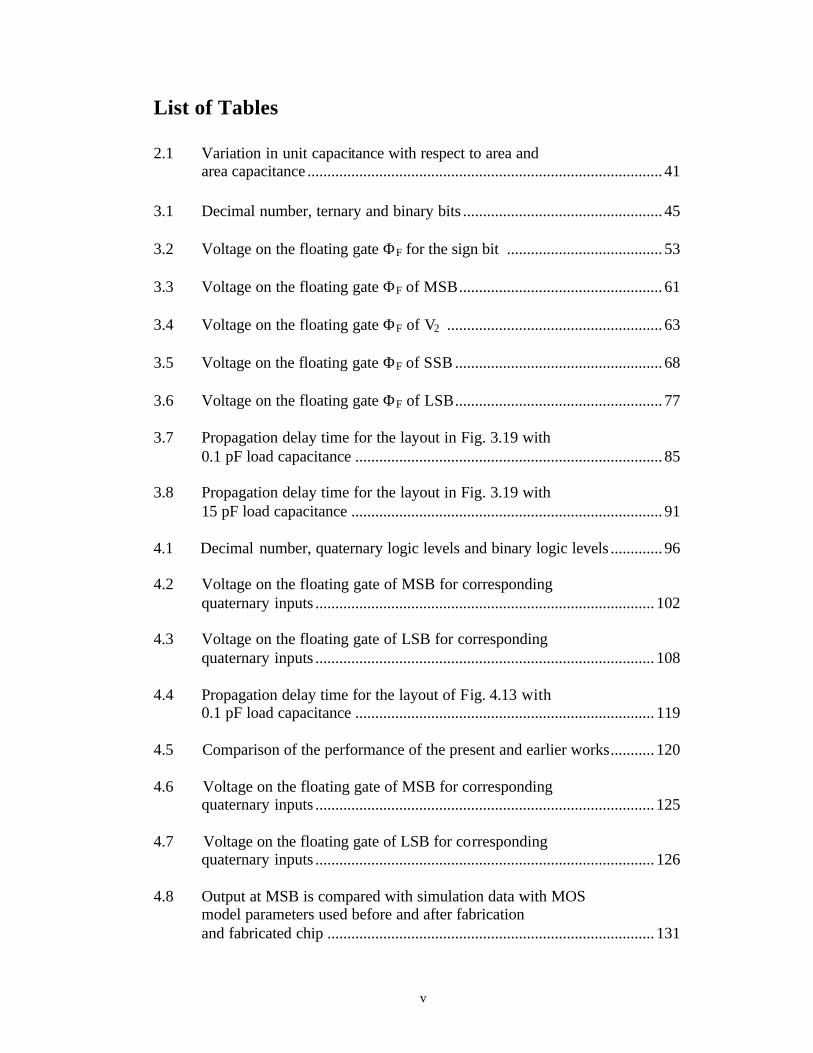
List of Tables
2.1 Variation in unit capacitance with respect to area and area capacitance ......................................................................................... 41
3.1 Decimal number, ternary and binary bits .................................................. 45 3.2 Voltage on the floating gate ΦF for the sign bit ....................................... 53 3.3 Voltage on the floating gate ΦF of MSB................................................... 61
3.4 Voltage on the floating gate ΦF of V2 ...................................................... 63 3.5 Voltage on the floating gate ΦF of SSB .................................................... 68 3.6 Voltage on the floating gate ΦF of LSB.................................................... 77 3.7 Propagation delay time for the layout in Fig. 3.19 with
0.1 pF load capacitance ............................................................................. 85 3.8 Propagation delay time for the layout in Fig. 3.19 with
15 pF load capacitance .............................................................................. 91 4.1 Decimal number, quaternary logic levels and binary logic levels ............. 96 4.2 Voltage on the floating gate of MSB for corresponding
quaternary inputs ..................................................................................... 102
4.3 Voltage on the floating gate of LSB for corresponding quaternary inputs ..................................................................................... 108
4.4 Propagation delay time for the layout of Fig. 4.13 with
0.1 pF load capacitance ........................................................................... 119
4.5 Comparison of the performance of the present and earlier works........... 120 4.6 Voltage on the floating gate of MSB for corresponding
quaternary inputs ..................................................................................... 125 4.7 Voltage on the floating gate of LSB for corresponding
quaternary inputs ..................................................................................... 126 4.8 Output at MSB is compared with simulation data with MOS
model parameters used before and after fabrication and fabricated chip .................................................................................. 131
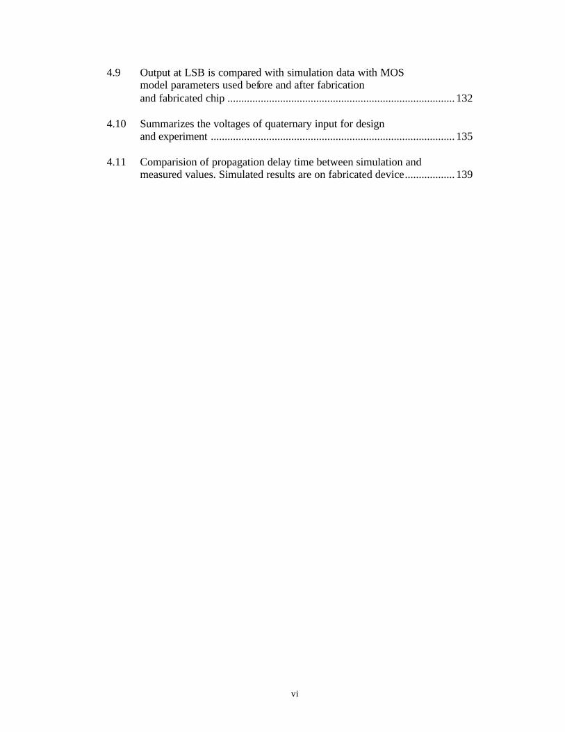
vi
4.9 Output at LSB is compared with simulation data with MOS model parameters used before and after fabrication and fabricated chip .................................................................................. 132
4.10 Summarizes the voltages of quaternary input for design and experiment ........................................................................................ 135 4.11 Comparision of propagation delay time between simulation and
measured values. Simulated results are on fabricated device.................. 139

vii
List of Figures
1.1 Logic levels used for a ternary logic ............................................................ 2
1.2 Logic levels used for a quaternary logic ....................................................... 3
1.3 The block diagram for radix converting read only memory (RCROM)....... 7 1.4 Block diagram for the conversion from multivalued to binary logic
using switched capacitor array technique .................................................... 9
1.5 Block diagram for conversion from eight bit binary number to six bit ternary number using Josephson junction technology............................... 11
1.6 Schematic diagram of cell shown in Fig. 1.5 ............................................ 12 2.1 Basic structure of a multiple- input floating gate MOSFET ...................... 15 2.2 Relationship among terminal voltages and coupling capacitances
of a multiple- input floating gate MOSFET............................................... 16
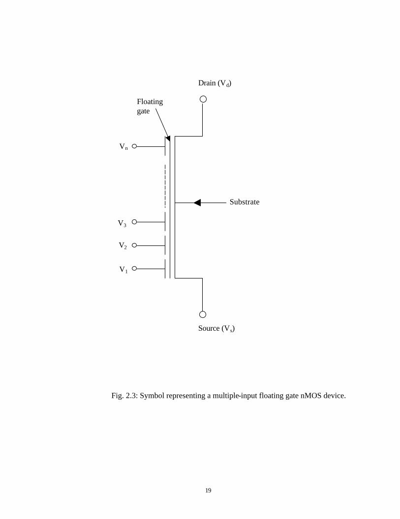
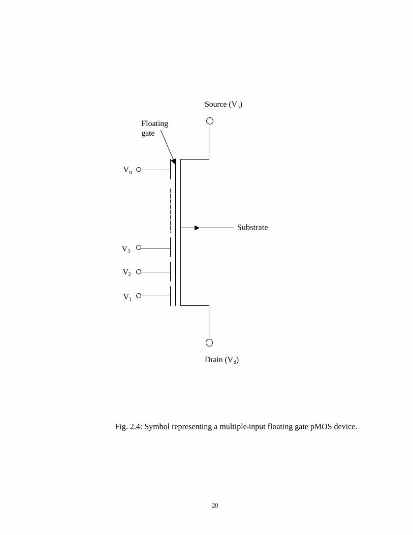
2.3 Symbol representing a multiple- input floating gate nMOS device........... 19 2.4 Symbol representing a multiple- input floating gate pMOS device........... 20 2.5 Circuit diagram to obtain I-V characteristics of a floating gate
nMOS transistor......................................................................................... 21
2.6 Circuit diagram to obtain I-V characteristics of a floating gate pMOS transistor......................................................................................... 22
2.7 I-V characteristics of a floating gate nMOS transistor .............................. 24 2.8 I-V characteristics of a floating gate pMOS transistor .............................. 25 2.9 Transfer curve for floating gate nMOS transistor (Ids Vs Vgs) .................. 26 2.10 Transfer curve for floating gate pMOS transistor (Ids Vs Vgs) .................. 27 2.11 CMOS inverter using MIFG MOSFETs ................................................... 28 2.12 Voltage transfer characteristics of a CMOS inverter with
W/L = 8 µm/1.6 µm (Φg0 = 0.68 V and Φs1 = 2.22 V)............................. 30
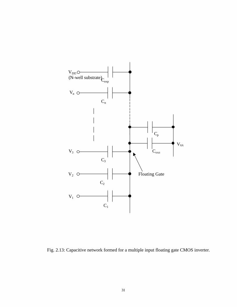
2.13 Capacitive network formed for a multiple input floating gate CMOS inverter....................................................................................................... 31
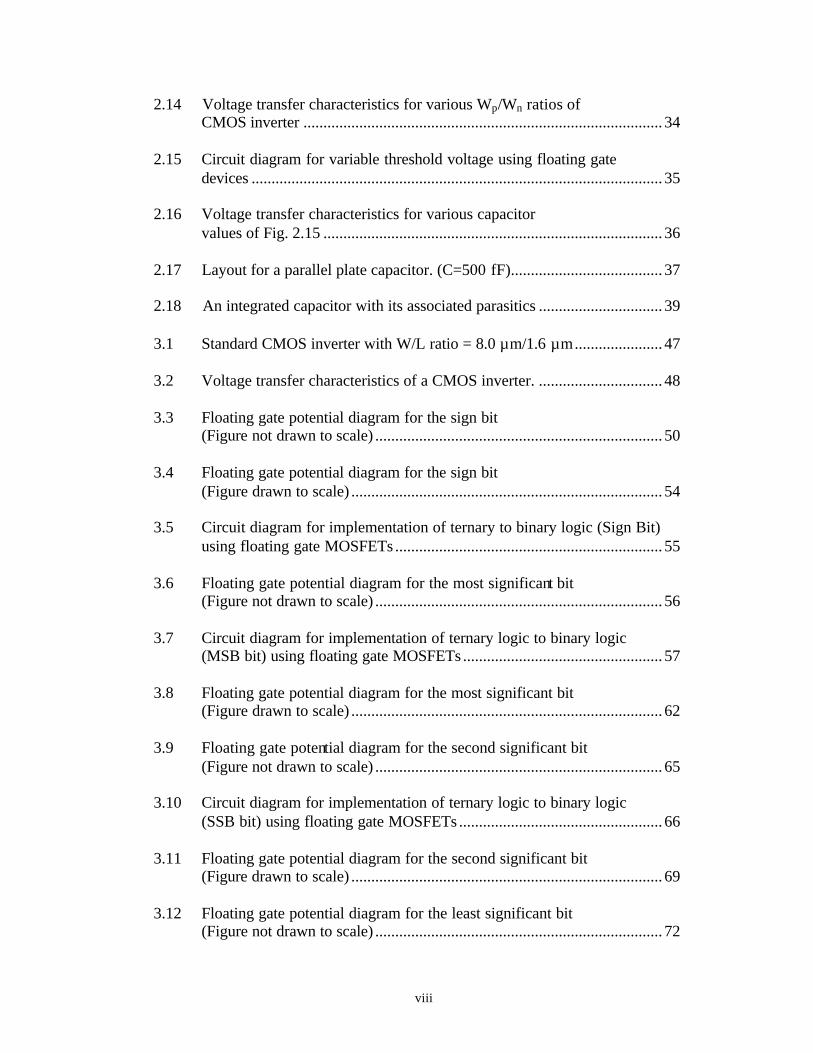
viii
2.14 Voltage transfer characteristics for various Wp/Wn ratios of CMOS inverter .......................................................................................... 34
2.15 Circuit diagram for variable threshold voltage using floating gate
devices ....................................................................................................... 35
2.16 Voltage transfer characteristics for various capacitor values of Fig. 2.15 ..................................................................................... 36 2.17 Layout for a parallel plate capacitor. (C=500 fF)...................................... 37 2.18 An integrated capacitor with its associated parasitics ............................... 39 3.1 Standard CMOS inverter with W/L ratio = 8.0 µm/1.6 µm...................... 47 3.2 Voltage transfer characteristics of a CMOS inverter. ............................... 48 3.3 Floating gate potential diagram for the sign bit
(Figure not drawn to scale) ........................................................................ 50 3.4 Floating gate potential diagram for the sign bit
(Figure drawn to scale) .............................................................................. 54 3.5 Circuit diagram for implementation of ternary to binary logic (Sign Bit)
using floating gate MOSFETs ................................................................... 55
3.6 Floating gate potential diagram for the most significant bit (Figure not drawn to scale) ........................................................................ 56
3.7 Circuit diagram for implementation of ternary logic to binary logic
(MSB bit) using floating gate MOSFETs .................................................. 57
3.8 Floating gate potential diagram for the most significant bit (Figure drawn to scale) .............................................................................. 62
3.9 Floating gate potential diagram for the second significant bit (Figure not drawn to scale) ........................................................................ 65
3.10 Circuit diagram for implementation of ternary logic to binary logic (SSB bit) using floating gate MOSFETs ................................................... 66
3.11 Floating gate potential diagram for the second significant bit (Figure drawn to scale) .............................................................................. 69
3.12 Floating gate potential diagram for the least significant bit (Figure not drawn to scale) ........................................................................ 72
ix
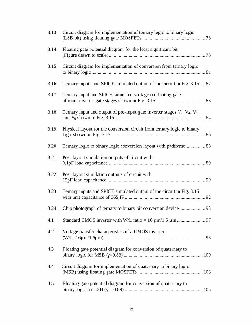
3.13 Circuit diagram for implementation of ternary logic to binary logic (LSB bit) using floating gate MOSFETs ................................................... 73
3.14 Floating gate potential diagram for the least significant bit (Figure drawn to scale) .............................................................................. 78
3.15 Circuit diagram for implementation of conversion from ternary logic to binary logic ............................................................................................ 81
3.16 Ternary inputs and SPICE simulated output of the circuit in Fig. 3.15 .... 82
3.17 Ternary input and SPICE simulated vo ltage on floating gate
of main inverter gate stages shown in Fig. 3.15 ........................................ 83
3.18 Ternary input and output of pre- input gate inverter stages V2, V4, V7 and V9 shown in Fig. 3.15 ......................................................................... 84
3.19 Physical layout for the conversion circuit from ternary logic to binary logic shown in Fig. 3.15 ............................................................................ 86
3.20 Ternary logic to binary logic conversion layout with padframe ............... 88 3.21 Post-layout simulation outputs of circuit with
0.1pF load capacitance .............................................................................. 89 3.22 Post-layout simulation outputs of circuit with
15pF load capacitance ............................................................................... 90 3.23 Ternary inputs and SPICE simulated output of the circuit in Fig. 3.15
with unit capacitance of 365 fF ................................................................. 92 3.24 Chip photograph of ternary to binary bit conversion device ..................... 93 4.1 Standard CMOS inverter with W/L ratio = 16 µm/1.6 µm....................... 97 4.2 Voltage transfer characteristics of a CMOS inverter
(W/L=16µm/1.6µm).................................................................................. 98
4.3 Floating gate potential diagram for conversion of quaternary to binary logic for MSB (γ=0.83) ................................................................ 100
4.4 Circuit diagram for implementation of quaternary to binary logic (MSB) using floating gate MOSFETs..................................................... 103
4.5 Floating gate potential diagram for conversion of quaternary to binary logic for LSB (γ = 0.89) ............................................................... 105
x
4.6 Circuit diagram for implementation of quaternary logic to binary logic (LSB) using floating gate MOSFETs ............................................. 106
4.7 Circuit diagram for implementing conversion of quaternary logic to binary logic using floating gate MOSFETs ......................................... 110
4.8 Quaternary input and SPICE simulated output (MSB) for the circuit in Fig. 4.4 ..................................................................................... 112
4.9 Quaternary input and SPICE simulated output (LSB) for the circuit in Fig. 4.6 ..................................................................................... 113
4.10 Voltage on floating gate of MSB in Fig. 4.4 from SPICE simulations ... 114 4.11 Voltage on floating gate of LSB in Fig. 4.6 from SPICE simulations .... 115 4.12 Pre-layout SPICE simulated output of circuit in Fig. 4.7 for all possible
combinations of quaternary input ............................................................ 116
4.13 Physical design of the conversion circuit from quaternary logic to binary logic shown in Fig. 4.7. (layout area = 181 × 128 µm2).......................... 117
4.14 Quaternary input and post layout outputs with 0.1pF load capacitance ... 118 4.15 SPICE simulated output of circuit in Fig. 4.7 for all possible
combinations of Quaternary input (unit capacitance =365 fF)................ 121 4.16 Photomicrograph of chip fabricated by MOSIS in standard double
polysilicon CMOS process...................................................................... 123 4.17 Voltage transfer characteristics of a CMOS inverter with
W/L=16 µm/1.6 µm with MOS model parameters of a fabricated design124 4.18 Quaternary input and SPICE simulated output (MSB) for the circuit shown
in Fig.4.7 with MOS model parameters of the fabricated design............ 127 4.19 Quaternary input and SPICE simulated output (LSB) for the circuit shown
in Fig.4.7 with MOS model parameters of the fabricated design............ 128 4.20 Decoder circuit transfer characteristics ................................................... 130 4.21 Output MSB is compared with simulated output with MOS model
parameters used for (a) design (b) fabricated (c) measured .................... 133 4.22 Output LSB is compared with simulated output with MOS model
parameters used for (a) design (b) fabricated (c) measured .................... 134

xi
4.23 SPICE simulated output of circuit in Fig. 4.7 for all possible combinations of quaternary input with 0.1 pF load capacitance............. 136
4.24 Quaternary input and post-layout outputs with
0.1 pF load capacitance ........................................................................... 137 4.25 Post-layout simulation output with 15 pF load capacitance .................... 138
C.1 Equivalent circuit of a multiple- input floating gate inverter
for electrical simulations ......................................................................... 155 C.2 Resistor is added to equivalent circuit for simulation purpose ................ 156
xii
Abstract
Multiple- input floating gate MOSFETs and floating gate potential diagrams
have been used for conversion of ternary-valued input and quaternary-valued input
into corresponding binary-valued output in CMOS integrated circuit design
environment. The method is demonstrated through the design of a circuit for
conversion of ternary inputs 00 to -1-1 (decimal 0 to -4) and 00 to 11 (decimal 0 to
+4) into the corresponding binary bits and for conversion of quaternary inputs
(decimal 0 to 3) into the corresponding binary bits (binary 00 to 11) in a standard
1.5 µm digital CMOS technology. The physical design of the circuits is simulated
and tested with SPICE using MOSIS BSIM3 model parameters. The conversion
method is simple and compatible with the present CMOS process. The circuits
could be embedded in digital CMOS VLSI design architectures.
The conversion circuit for ternary inputs into corresponding binary outputs
has maximum propagation delay of 8 ns with 0.1 pF simulated capacitive load. The
physical layout design occupies an area of 432×908 µm2.
The conversion circuit for quaternary inputs to corresponding binary outputs
has maximum propagation delay of 6 ns with 0.1 pF simulated capacitive load. The
physical layout design occupies an area of 130×175 µm2. The conversion circuit
achieved significant improvement in the number of devices. A reduction of more
than 75% in transistor count was obtained over the previous designs. Measurements
of the fabricated devices for the conversion of quaternary input into binary output
agree with simulated values.
1
Chapter 1
Introduction
The performance of two level binary logic is limited due to interconnects
which occupy a large area on a VLSI chip. In a VLSI circuit, approximately 70
percent of the area is devoted to interconnection, 20 percent to insulation, and 10
percent to device [1]. One can achieve a more cost-effective way of utilizing
interconnections by using a larger set of signals over the same area in multiple-
valued logic (MVL) devices [2,3], allowing easy implementation of circuits. In
MVL devices, the noise advantage of binary logic is retained. The higher radix in
use is the ternary (radix-3) and the quaternary (radix-4). Two logic systems are
available in ternary logic, balanced ternary logic -1, 0 and 1 and simple ternary logic
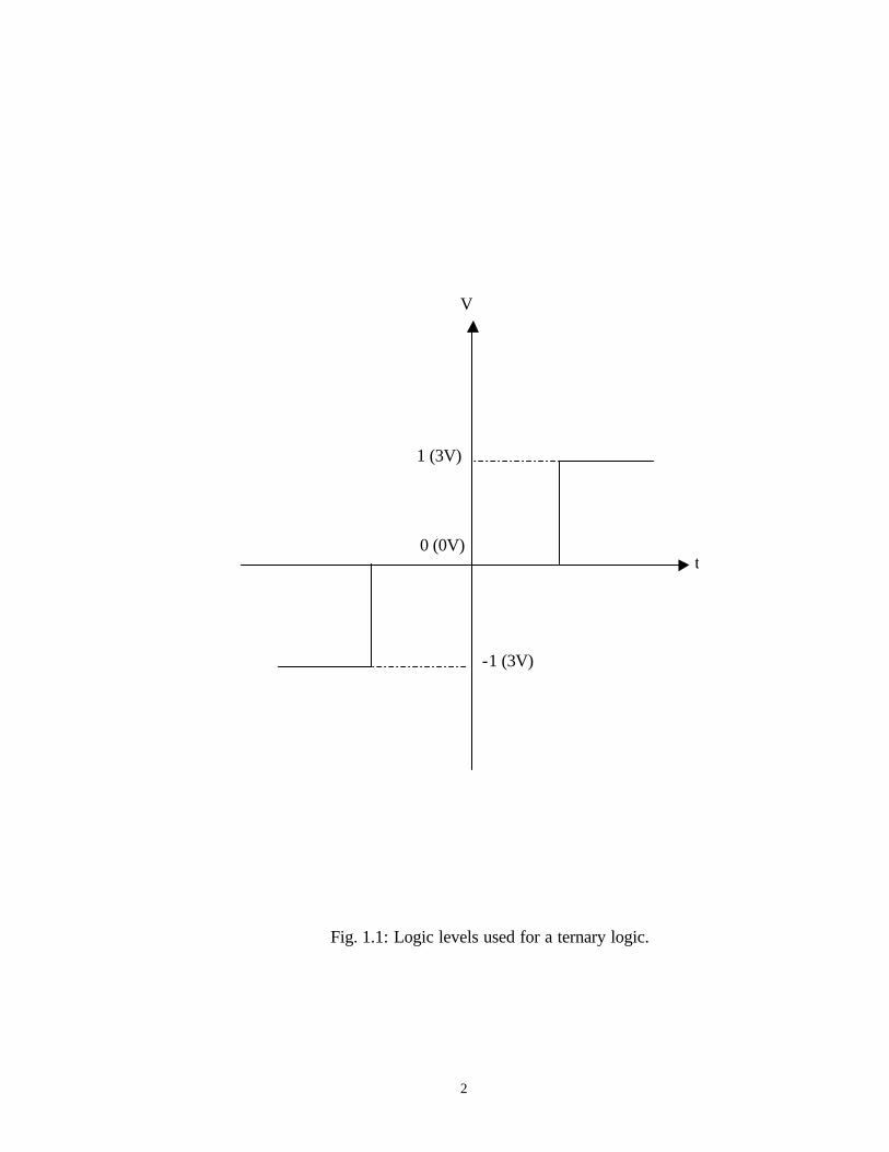
0, 1 and 2. The quaternary logic uses 0, 1, 2 and 3 logic levels. Figure 1.1 shows
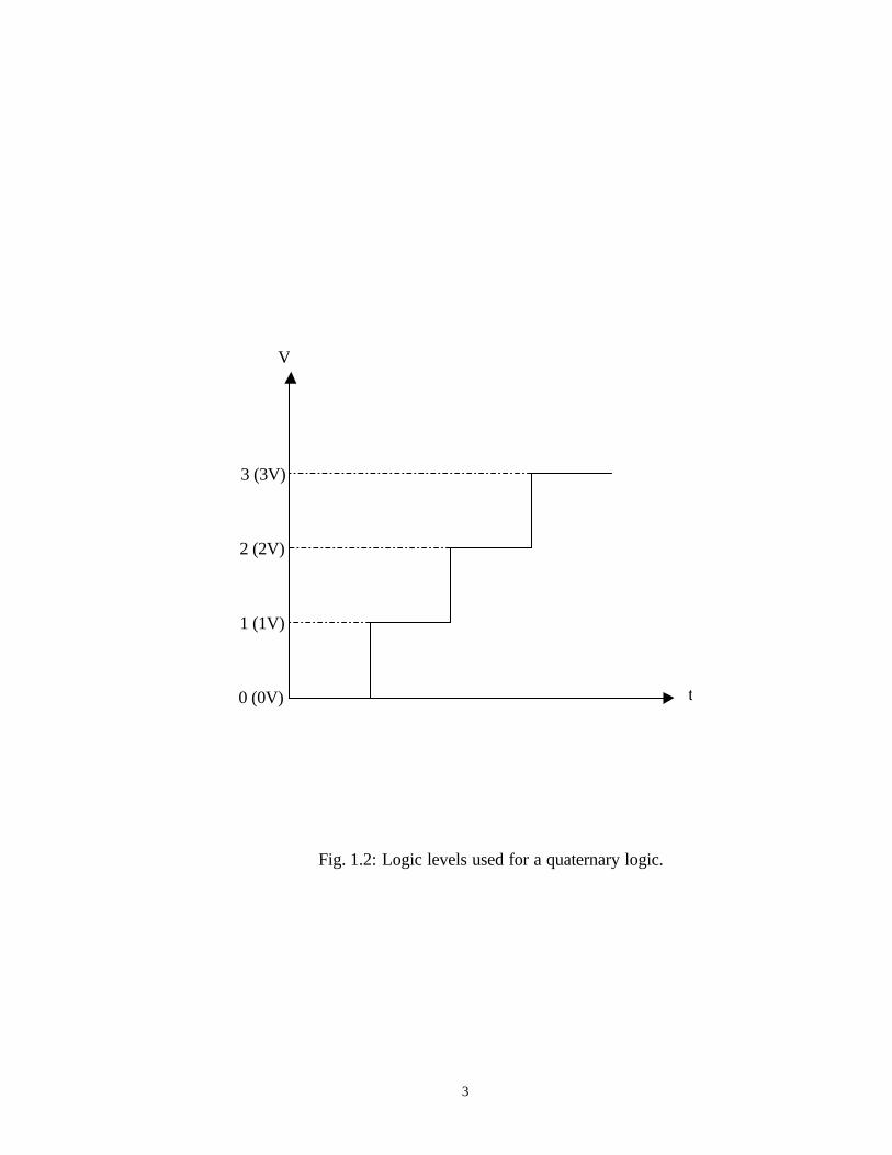
ternary logic with a 3 V supply voltage. Figure 1.2 shows quaternary logic levels.
In any numerical system, the smaller the radix the larger the number of digits
required to present a given quantity. The number necessary to express a range N is
given by N = Rd where R is the radix and d is the necessary number of digits,
rounded up to the next highest integer. The cost and complexity C of system
hardware is proportional to the digit capacity R×d [3], then
=×=
RN
RkdRkCloglog
)( (1.1)
where k is constant. Differentiating with respect to R will show that for minimum
cost C, R should be equal to e = 2.718. Since in practice R must be an integer, this
suggests that R = 3 (ternary) would be more economical than R = 2 (binary) [3].
2
Fig. 1.1: Logic levels used for a ternary logic.
0 (0V)
-1 (3V)
1 (3V)
t
V
3
Fig. 1.2: Logic levels used for a quaternary logic.
0 (0V)
1 (1V)
2 (2V)
3 (3V)
t
V
4
If it is assumed that circuit cost and complexity C for processing one signal line
remains constant irrespective of radix, then total system cost C is merely
proportional to d. In this case
==
RN
kkdCloglog
(1.2)
which is a gradually decreasing cost with increasing radix R.
The ternary logic system is represented in two different logic levels; simple
(or “unsigned”) ternary logic levels 0, 1 and 2 and balanced (or “signed”) ternary
logic levels –1, 0 and +1. The balanced ternary logic level system has added
mathematical advantages in numerical representation and in arithmetic operations
over the simple ternary logic system [3,4]. It can represent both positive and
negative numbers without using an unary minus. The negative of a number is
obtained by interchanging +1 and –1. Addition and multiplication are almost as
simple as for the binary, cases with no digits larger than 1 in the tables. It follows
that addition and subtraction may be performed with the same hardware in balanced
ternary system by sign changes of the addend or subtractend, respectively as
required. Simple algorithms are available for division. The operation of rounding to
the nearest integer is identical to truncation (i.e., deleting everything to the right of
the radix point). Ternary arithmetic with both unsigned and balanced (signed)
encoding is found in [5]. It is shown that the balanced ternary provides a significant
reduction in the gate count in comparison to binary and unsigned ternary systems,
but at the expense of an increased logic delay.
5
In a standard CMOS process with supply voltage of 3 V, the logic level -1, 0
and 1 is defined as -3 V, 0 V and 3 V, respectively. The advantage of an odd valued
radix in a complex number multiplier suitable for applications such as discrete
Fourier transform has been demonstrated [6]. Wu [7] has listed the advantages and
disadvantages of using multi-valued logic implemented with in integrated circuits.
He discussed the reasons for focusing on the ternary logic over quaternary logic in
terms of cost and complexity, characteristics and additional hardware required. The
ternary logic has better noise margin and noise immunity when compared to
quaternary logic because of the use of two different voltage sources. The power
dissipation is higher in ternary logic circuits, as the peak-to-peak voltage of ternary
logic is twice that of binary logic circuits. Srivastava and Venkatapathy [8] have
demonstrated that ternary logic circuits could be implemented in standard CMOS
process with voltage supply as low as 1 V.
In order to make use of the advantages of multi-valued logic, the structure of
mixed radix system using multi-valued and binary logic is more appropriate than
use of only multi-valued logic [9,10]. Therefore, it will be necessary to provide
encoding and decoding circuitry to perform the required conversion between multi-
valued logic signaling on the bus and the binary logic processing circuits. The usage
of multi-valued circuits over binary circuits deals with the circuit complexity of
encoder and decoder and other circuits for the same case. Lack of simple encoder
and decoder schemes for the multi-valued system reduces the effective usage of
MVL circuits in VLSI circuits. In the present work, floating gate MOSFETs are
used to simplify the design of conversion circuits.
6
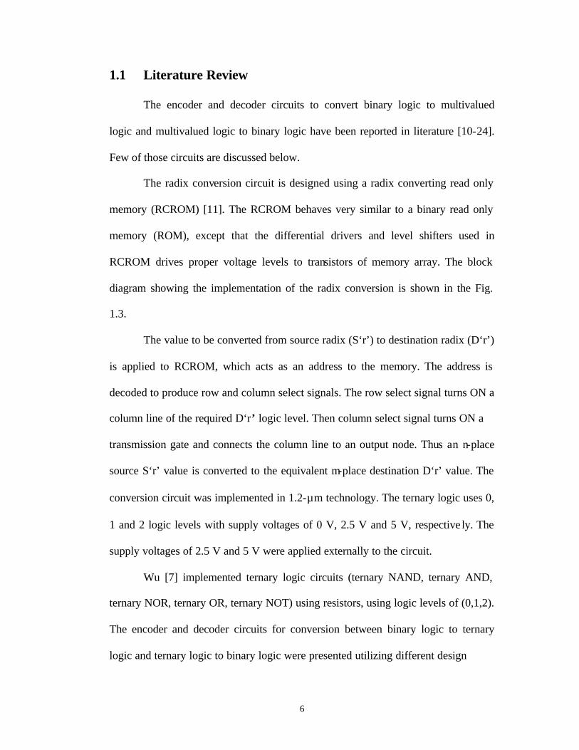
1.1 Literature Review
The encoder and decoder circuits to convert binary logic to multivalued
logic and multivalued logic to binary logic have been reported in literature [10-24].
Few of those circuits are discussed below.
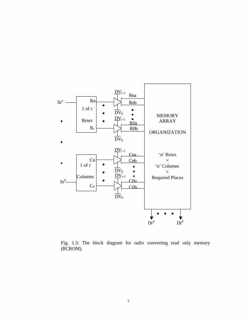
The radix conversion circuit is designed using a radix converting read only
memory (RCROM) [11]. The RCROM behaves very similar to a binary read only
memory (ROM), except that the differential drivers and level shifters used in
RCROM drives proper voltage levels to transistors of memory array. The block
diagram showing the implementation of the radix conversion is shown in the Fig.
1.3.
The value to be converted from source radix (S‘r’) to destination radix (D‘r’)
is applied to RCROM, which acts as an address to the memory. The address is
decoded to produce row and column select signals. The row select signal turns ON a
column line of the required D‘r’ logic level. Then column select signal turns ON a
transmission gate and connects the column line to an output node. Thus an n-place
source S‘r’ value is converted to the equivalent m-place destination D‘r’ value. The
conversion circuit was implemented in 1.2-µm technology. The ternary logic uses 0,
1 and 2 logic levels with supply voltages of 0 V, 2.5 V and 5 V, respective ly. The
supply voltages of 2.5 V and 5 V were applied externally to the circuit.
Wu [7] implemented ternary logic circuits (ternary NAND, ternary AND,
ternary NOR, ternary OR, ternary NOT) using resistors, using logic levels of (0,1,2).
The encoder and decoder circuits for conversion between binary logic to ternary
logic and ternary logic to binary logic were presented utilizing different design
7
Fig. 1.3: The block diagram for radix converting read only memory (RCROM).
1 of n Rows
Rn
R0
C0
Cn 1 of n
Columns
DVr-1
DV0 DVr-1
DV0
DVr-1
DV0 DVr-1
DV0
Srn
Sr0
Rnb Rna
R0a R0b
Cna Cnb
C0aC0b
MEMORY ARRAY
ORGANIZATION
‘n’ Rows ×
‘n’ Columns ×
Required Places
Dr0Drn
8
techniques. The decoder circuits were designed by i) altering the width to length
ratio of CMOS transistors, by ii) using pad MOS transistors and by iii) using multi-
threshold CMOS transistors. In i), the width to length ratio is adjusted such that the
threshold voltage of inverter is set to obtain the binary outputs. In ii), stacking an
nMOS transistor at ground or pMOS transistor at power supply changes the
threshold voltage, which gives the binary output. In iii), MOSFETs with different
threshold voltages are designed.
Wu and Huang [12] presented a parallel-pipelined multiplier using dynamic
ternary logic circuits. The multiplier is reported to have lesser device count,
increased operating frequency, lesser latency, power dissipation and chip area. The
basic design of multiplier uses a block, which converts radix-2 redundant positive
digit number (0,1,2) to binary (0,1). The converter is implemented using dynamic
logic with clock Φ, and by adjusting the threshold voltages such that binary output
is produced at clock edges.
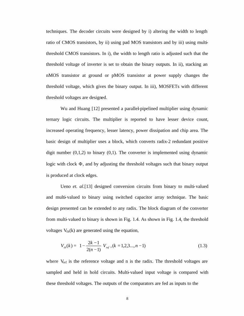
Ueno et. al.[13] designed conversion circuits from binary to multi-valued
and multi-valued to binary using switched capacitor array technique. The basic
design presented can be extended to any radix. The block diagram of the converter
from multi-valued to binary is shown in Fig. 1.4. As shown in Fig. 1.4, the threshold
voltages Vth(k) are generated using the equation,
)1...,3,2,1(,)1(2
121)( −=
−−
−= nkVnk
kV refth (1.3)
where Vref is the reference voltage and n is the radix. The threshold voltages are
sampled and held in hold circuits. Multi-valued input voltage is compared with
these threshold voltages. The outputs of the comparators are fed as inputs to the
9
Fig. 1.4: Block diagram for the conversion from multivalued to binary logic using switched capacitor array technique.
Radix n Multivalued input
Threshold Voltage Generator
Hold Circuits
Comparator
Decoder
Binary Output
Vth(1) Vth(2) Vth(n)
10
decoding circuit, which generates binary output. The accuracy of the decoder
depends on the generation of threshold voltages. The circuit configuration uses
capacitors to generate the threshold voltage, which allows the design to be extended
for large radices without loosing accuracy.
The above design is applied for the conversion from ternary logic (n=3) to
binary logic (n=2). Using equation (1.3), the threshold voltages to be generated are
Vth(1) = 3/4Vref and Vth(2) = 1/4Vref. The ternary input 0 (0V), 1 (1/2Vref) or 2 (Vref)
when applied to the circuit are compared with the thresholds 1/4Vref and 3/4Vref and
decoded to give binary output.
Li et. al. [14] proposed conversion technique from binary to balanced
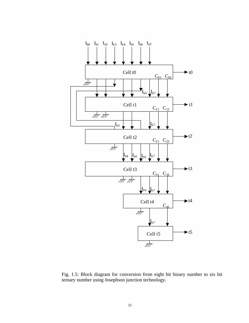
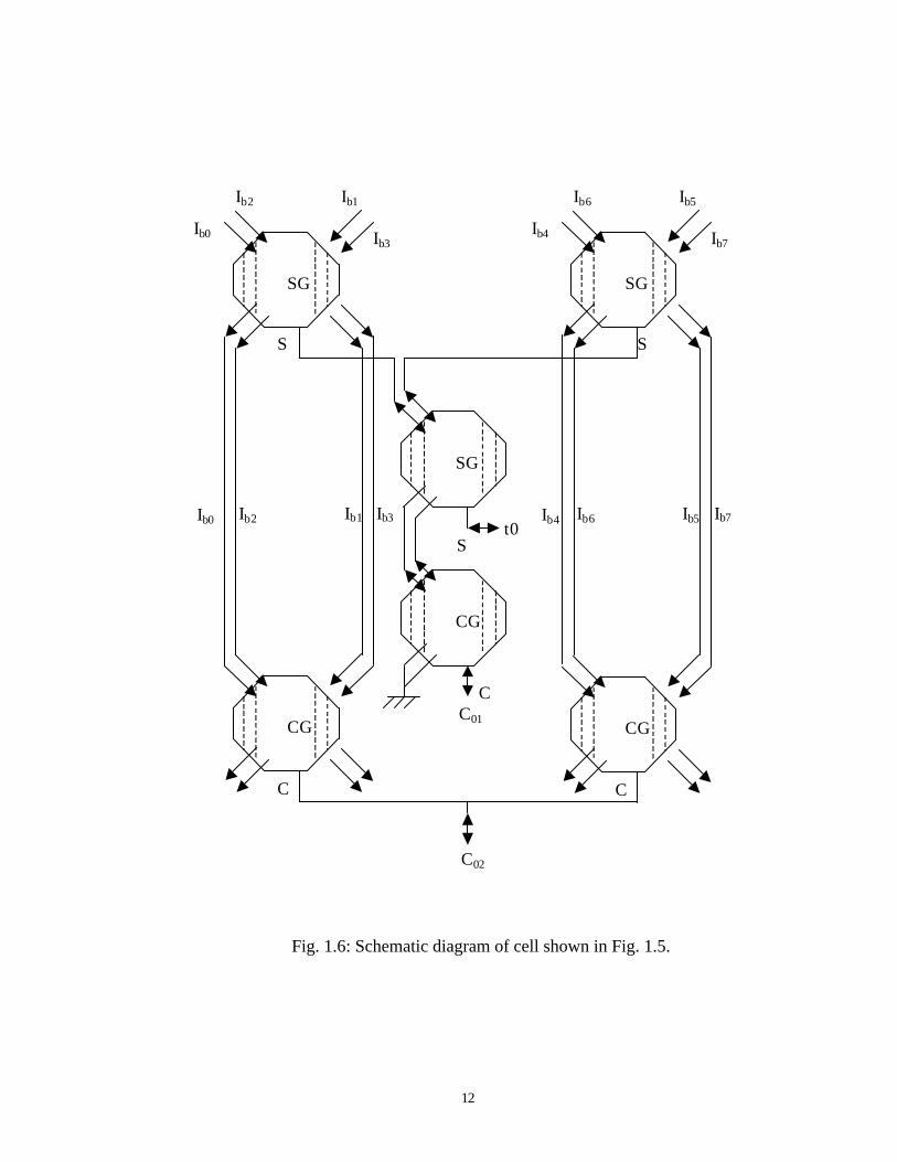
ternary logic (-1,0,1) based on Josephson technology. They converted an eight bit
binary number to six bit ternary number. The schematic diagram of binary to ternary
converter for 8-bit binary number constructed using six cells is shown in Fig. 1.5.
The basic structure of the cell used in Fig. 1.5 is shown in Fig. 1.6, where (Ib0, …,
Ib7) is 8 bit binary input. The symbol SG is sum circuit to produce ternary output ‘t’
and CG is carry circuit to produce C01 or C02. The SG and CG circuits are
constructed with Josephson complementary ternary logic (JCTL), which exhibits
symmetrical I-V characteristics. In summary, the decoder circuits found in literature
converted ternary logic (0, 1, 2) to binary logic (0, 1). Few encoder and decoder
[8,13-21] circuits for conversion from binary to quaternary (0, 1, 2, 3) and
quaternary to binary are found in literature. The present work focuses on conversion
from balanced ternary logic (-1, 0, 1) to binary logic using floating gate MOSFETs.
11
Fig. 1.5: Block diagram for conversion from eight bit binary number to six bit ternary number using Josephson junction technology.
Cell t0
Cell t1
Cell t2
Cell t3
Cell t4
Cell t5
t0
t1
t2
t3
t4
t5
Ib0 Ib1 Ib2 Ib3 Ib4 Ib5 Ib6 Ib7
Ib6 Ib7
C01 C02
C11 C12
C21 C22
C31 C32
C41
Ib7 Ib3
Ib4 Ib5 Ib6 Ib7
Ib7 Ib6
Ib7
12
Fig. 1.6: Schematic diagram of cell shown in Fig. 1.5.
SG
CG
Ib0
Ib2 Ib1
Ib3
SG
Ib4
Ib6 Ib5
Ib7
SG
S S
S t0
CG
C
CG
C
Ib0 Ib2 Ib1 Ib3 Ib4 Ib6 Ib5 Ib7
C
C02
C01
13
1.2 Chapter Organization
The basic structure and operation of floating gate devices is discussed in
Chapter 2. The design flow with simulation results obtained from SPICE, for
conversion from balanced ternary to binary logic is presented in Chapter 3. In
Chapter4, a scheme to convert quaternary to binary bit is presented. Chapter 5
concludes the present work. The circuit files used for simulations to obtain the I-V
characteristic curves of floating gate MOSFETs are listed in Appendix A. The MOS
model parameters used for design is presented in Appendix B. The MOS model
parameters of the fabricated chip are presented in Appendix D. Techniques used to
simulate floating gate devices in SPICE is presented in Appendix C.
14
Chapter 2
Multiple-Input Floating Gate MOSFET (MIFG MOSFET)
2.1 Introduction
The multiple- input floating gate devices are well known for EPROMs,
EEPROMs, and flash memories [24,25,26]. The primary principle is that the
polysilicon floating gate of MOS transistor, is insulated with silicon dioxide, and
hence, maintains stored charge for a long time. The floating gate devices are
implemented in a standard analog CMOS process. The floating gate MOSFETs are
used not just in digital memories but also in capacitive based circuits, in adaptive
circuit elements and in analog memory elements as well [27,28,29]. The floating
gate devices occupy a small layout area, have a high reliability for data computation
and have low power dissipation of the logic functions [30,31].
2.2 Basic Structure and Operation
The basic structure of the multiple- input floating gate MOSFET [32,33] is
shown in the Fig. 2.1. It consists of n-channel MOS transistor having a gate
electrode, which is electrically floating. The floating gate in the MOSFET extends
over the channel and the field oxide. Array of control gates, which are inputs to the
transistor, are formed over the floating gate using the second polysilicon layer. Fig.
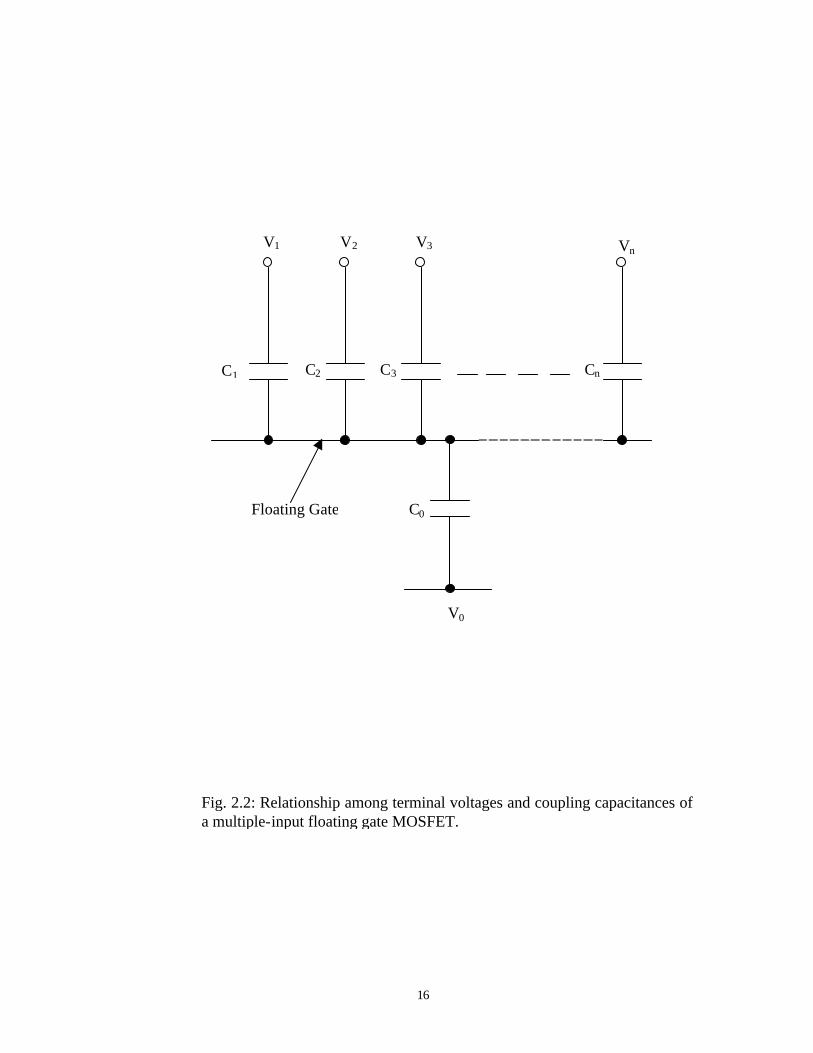
2.2 shows the capacitive coupling between the multiple input gates and the floating
gate and the channel. In Fig. 2.2, C1, C2, C3,…,Cn are the coupling capacitors
between the floating gate and the input corresponding to terminal voltages V1, V2,
V3,…,Vn, respectively. C0 is the capacitance between floating gate and substrate.
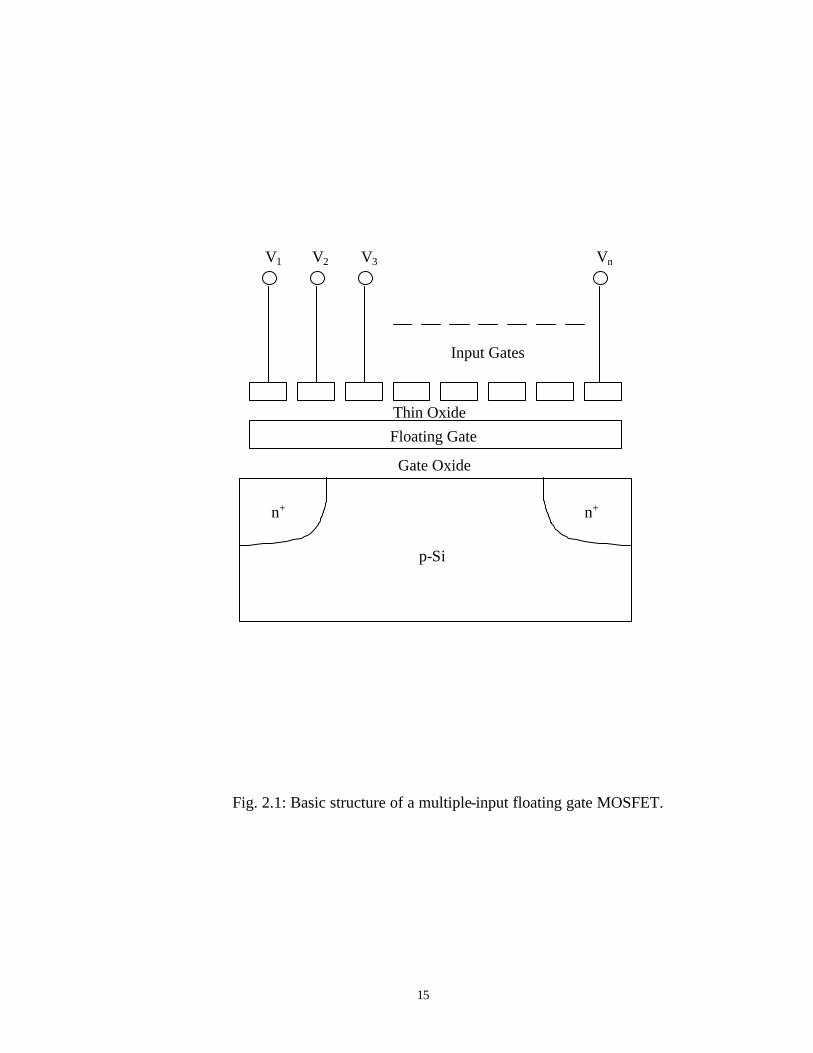
15
Fig. 2.1: Basic structure of a multiple-input floating gate MOSFET.
V1 V2 V3 Vn
Floating Gate
Input Gates
Thin Oxide
p-Si
n+ n+
Gate Oxide
16
Fig. 2.2: Relationship among terminal voltages and coupling capacitances of a multiple-input floating gate MOSFET.
V1 V2 V3 Vn
C1 C2 C3 Cn
C0
V0
Floating Gate
17
Q1, Q2, Q3,...Qn are the charges stored in corresponding capacitors C1, C2, C3,…,Cn,
respectively. At any given time ‘t’, the net charge on the floating gate QF(t) is given
by [33],
∑∑==
−Φ=−+=n
iiFi
n
iiF tVtCtQQtQ
010 ))()(())(()( (2.1)
or ∑∑==
−Φ=n
iii
n
iiFF tVCCttQ
00
)()()( (2.2)
where n is the number of inputs, Q0 is the initial charge present on the floating gate,
Qi(t) is the charge present in the capacitor Ci at time ‘t’ and ΦF(t) is the potential at
the input of the floating gate. The law of conservation of charge states that the net
charge of an isolated system remains constant. Set V0 = 0 V and assuming that area
of capacitance is constant with time, applying conservation of charge at floating
gate, equation (2.2) can be expressed as follows,
∑∑∑∑====
−Φ=−Φn
iii
n
iiF
n
iii
n
iiF tVCCtVCC
1010
)()()0()0( (2.3)
or ∑∑∑∑====
−=Φ−Φn
iii
n
iii
n
iiF
n
iiF VCtVCCCt
1100
)0()()0()( (2.4)
or .)0()(
)0()(
0
11
∑
∑∑
=
==
−+Φ=Φ
n
ii
n
iii
n
iii
FF
C
VCtVCt (2.5)
Assuming zero initial charge on the floating gate, at equilibrium equation
(2.5) reduces to
.)(
)(
0
1
∑
∑
=
==Φn
ii
n
iii
F
C
tVCt (2.6)
18
The nMOS transistor is switched ON or OFF depending on whether ΦF(t) is
greater than or less than threshold voltage of the transistor. The symbol of nMOS
and pMOS floating gate transistors are shown in Figs. 2.3 and 2.4, respectively. The
voltage on the floating gate of the transistor is given by the equation (2.6). If Vs is
the voltage on the source of pMOS transistor then, the transistor is ON if
thpsF VV <−Φ )(
and the transistor is OFF if
thpsF VV >−Φ )(
where Vthp is threshold voltage of pMOSFET.
If Vs is the voltage on the source of nMOS transistor then, the transistor is ON if
thnsF VV >−Φ )(
and the transistor is OFF if
thnsF VV <−Φ )(
where Vthn is threshold voltage of nMOSFET.
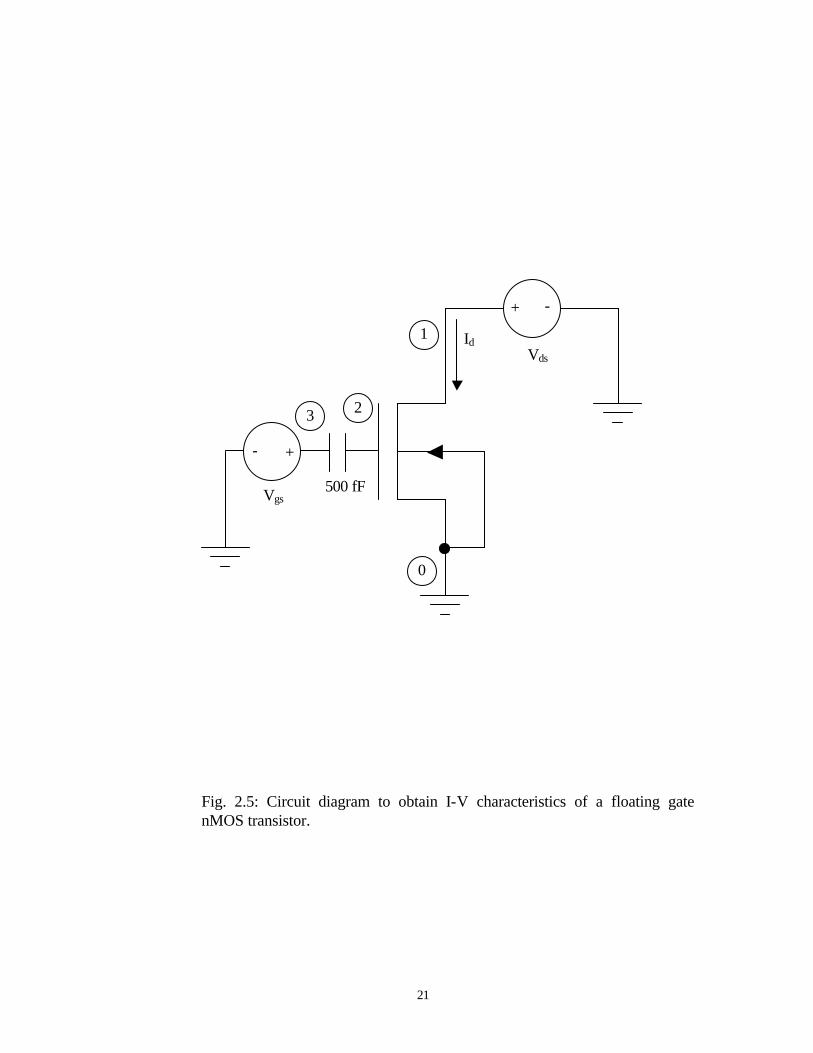
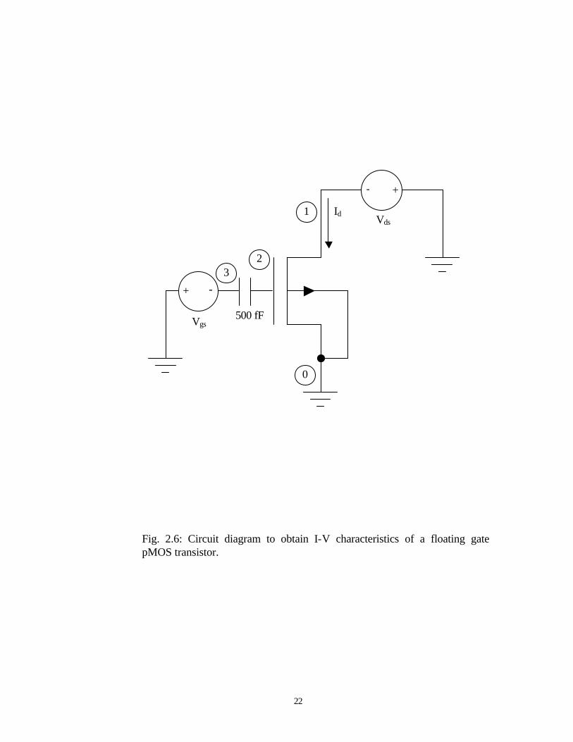
2.3 I–V Characteristics of MIFG Transistors
The circuits used for obtaining the I–V characteristic s of floating gate MOS
transistors are shown in Fig. 2.5 and Fig. 2.6, respectively. The circuits shown in
Figs. 2.5 and 2.6 have capacitors of 500 fF at the gate of the transistor. The
capacitor value 500 fF is the unit capacitance used in circuits here to plot the
characteristics of the floating gate transistors. While performing a DC analysis,
SPICE open circuits the capacitor, resulting in no input applied to the gate of the
transistor for a given value of Vgs. Hence, instead of performing DC analysis;
transient analysis is performed to obtain the characteristics.
19
Fig. 2.3: Symbol representing a multiple-input floating gate nMOS device.
V1
V2
V3
Source (Vs)
Vn
Drain (Vd)
Floating gate
Substrate
20
Fig. 2.4: Symbol representing a multiple-input floating gate pMOS device.
V1
V2
V3
Source (Vs)
Vn
Drain (Vd)
Floating gate
Substrate
21
Fig. 2.5: Circuit diagram to obtain I-V characteristics of a floating gate nMOS transistor.
+ -
- +
Vgs
Vds Id
500 fF
1
23
0
22
Fig. 2.6: Circuit diagram to obtain I-V characteristics of a floating gate pMOS transistor.
+-
-+
Vgs
Vds Id
500 fF
2
1
0
3
23
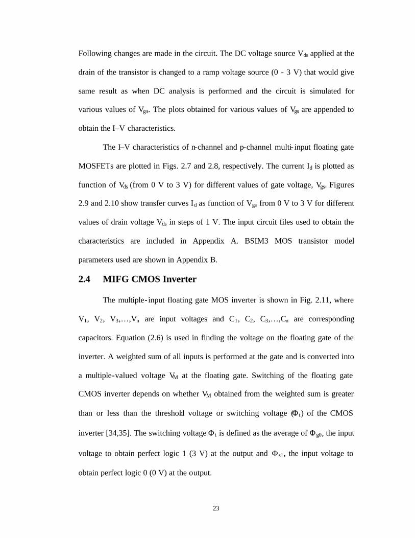
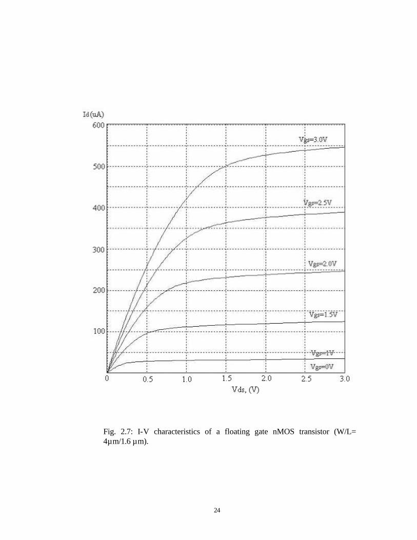
Following changes are made in the circuit. The DC voltage source Vds applied at the
drain of the transistor is changed to a ramp voltage source (0 - 3 V) that would give
same result as when DC analysis is performed and the circuit is simulated for
various values of Vgs. The plots obtained for various values of Vgs are appended to
obtain the I–V characteristics.
The I–V characteristics of n-channel and p-channel multi- input floating gate
MOSFETs are plotted in Figs. 2.7 and 2.8, respectively. The current Id is plotted as
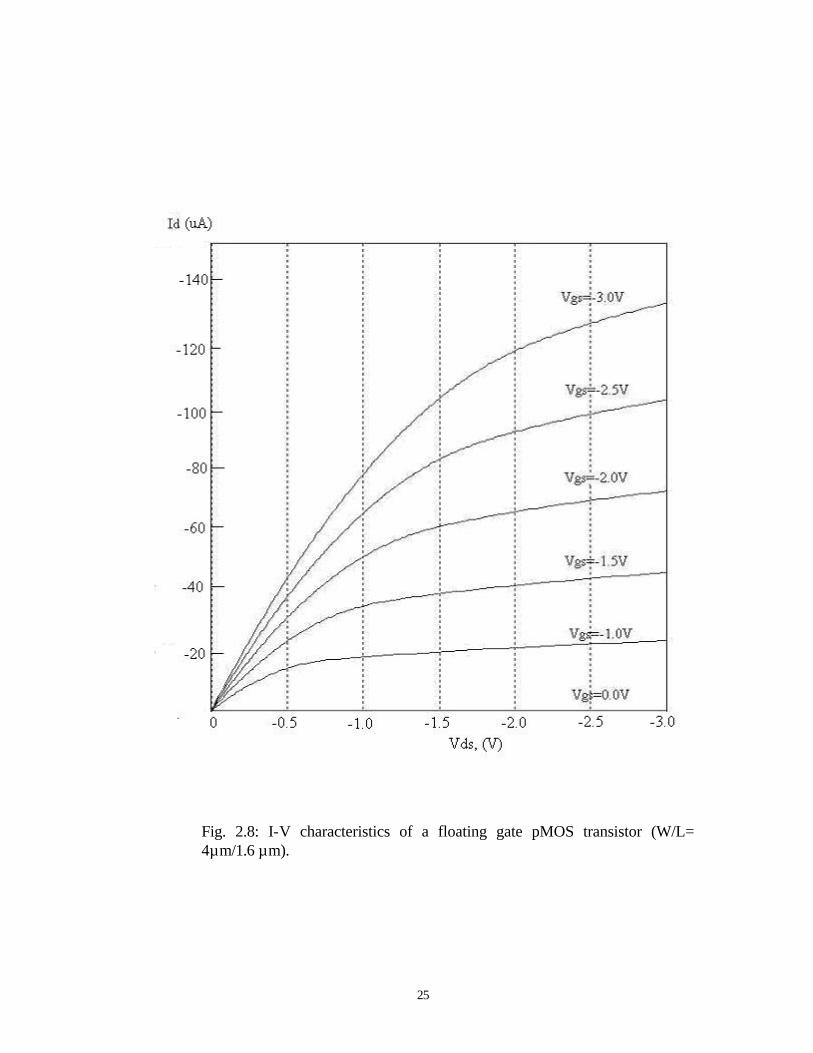
function of Vds (from 0 V to 3 V) for different values of gate voltage, Vgs. Figures
2.9 and 2.10 show transfer curves Id as function of Vgs from 0 V to 3 V for different
values of drain voltage Vds in steps of 1 V. The input circuit files used to obtain the
characteristics are included in Appendix A. BSIM3 MOS transistor model
parameters used are shown in Appendix B.
2.4 MIFG CMOS Inverter
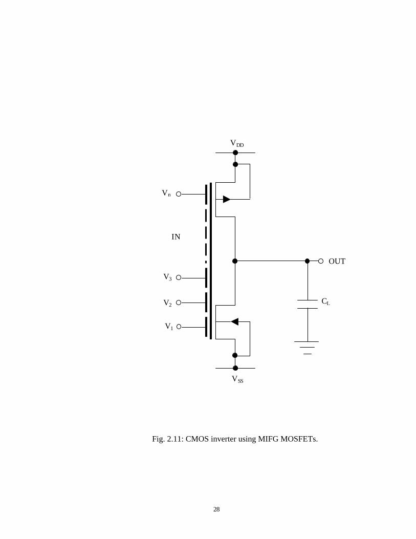
The multiple- input floating gate MOS inverter is shown in Fig. 2.11, where
V1, V2, V3,…,Vn are input voltages and C1, C2, C3,…,Cn are corresponding
capacitors. Equation (2.6) is used in finding the voltage on the floating gate of the
inverter. A weighted sum of all inputs is performed at the gate and is converted into
a multiple-valued voltage VM at the floating gate. Switching of the floating gate
CMOS inverter depends on whether VM obtained from the weighted sum is greater
than or less than the threshold voltage or switching voltage (Φt) of the CMOS
inverter [34,35]. The switching voltage Φt is defined as the average of Φg0, the input
voltage to obtain perfect logic 1 (3 V) at the output and Φs1, the input voltage to
obtain perfect logic 0 (0 V) at the output.
24
Fig. 2.7: I-V characteristics of a floating gate nMOS transistor (W/L= 4µm/1.6 µm).
25
Fig. 2.8: I-V characteristics of a floating gate pMOS transistor (W/L= 4µm/1.6 µm).
26
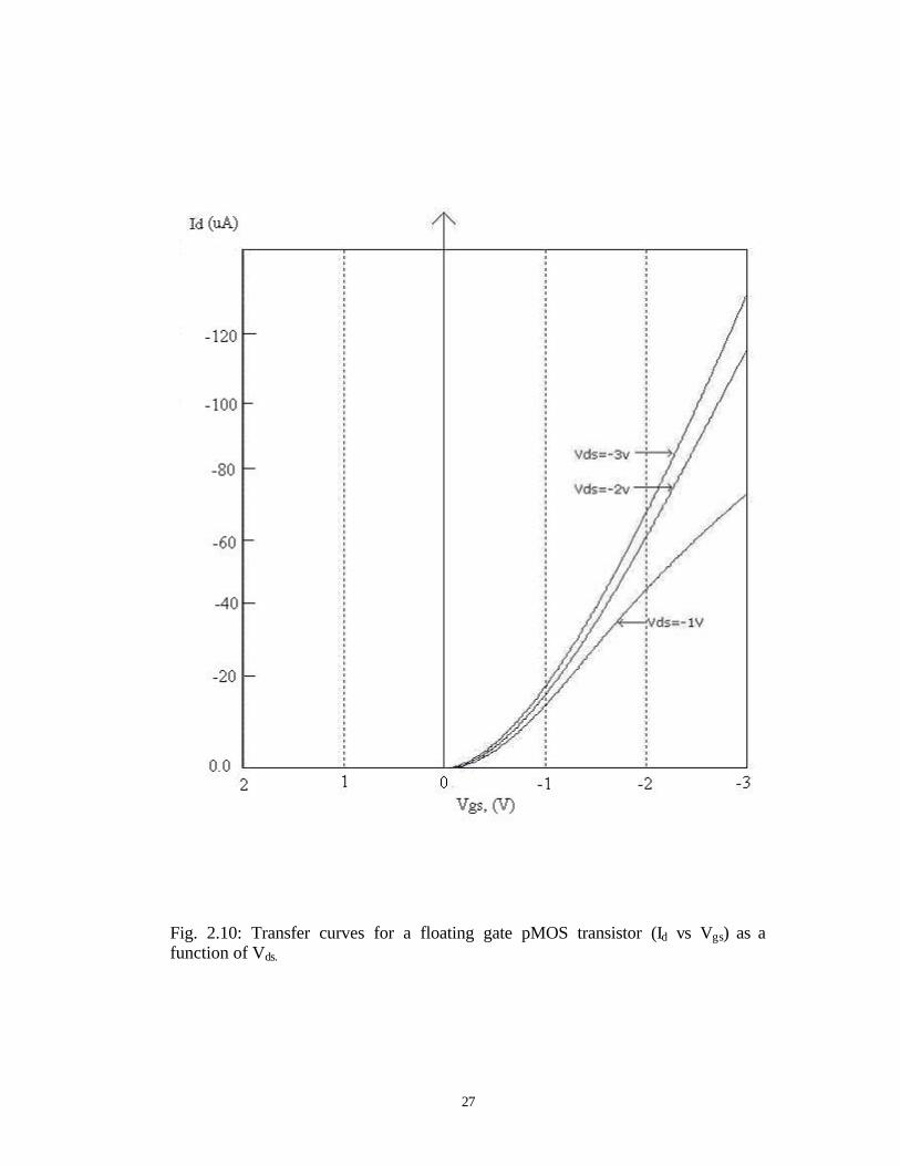
Fig. 2.9: Transfer curves for floating gate nMOS transistor (Id vs Vgs) as a function of Vds.
27
Fig. 2.10: Transfer curves for a floating gate pMOS transistor (Id vs Vgs) as a function of Vds.
28
Fig. 2.11: CMOS inverter using MIFG MOSFETs.
V3
OUT
CL
VDD
VSS
Vn
V1
V2
IN
29
( )
.2
10 sgt
Φ+Φ=Φ (2.7)
Hence, the output (Vout) of floating gate CMOS inverter is given by,
Vout = HIGH (3 V) if ΦF < Φt
= LOW (0 V) if ΦF > Φt (2.8)
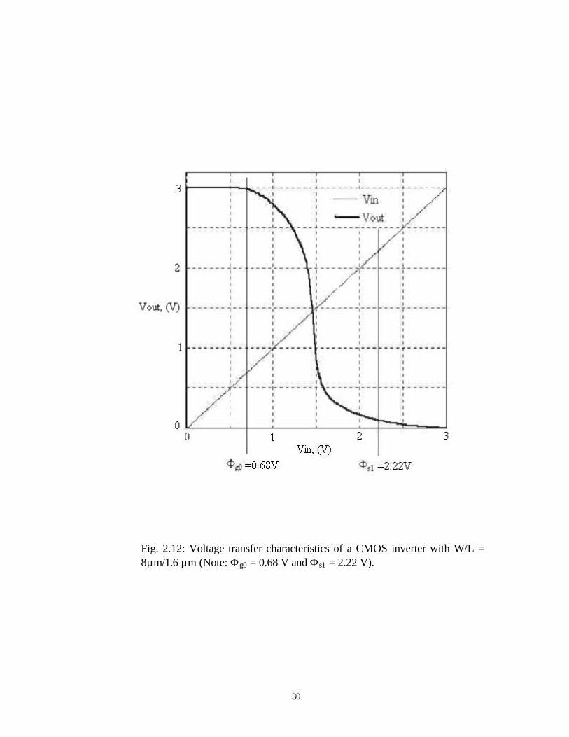
Φg0 and Φs1 are obtained from voltage transfer characteristic of a CMOS inverter.
The latter is shown in Fig. 2.12 for W/L=8.0 µm/1.6 µm. The values of Φg0 and Φs1
are also shown in the Fig 2.12. Φg0 and Φs1 are the input voltages at which the
output Vout is VDD-0.1V and 0.1 V, respectively.
The capacitor network formed for the n- input floating gate inverter is shown
in Fig. 2.13. The gate oxide capacitance of pMOS transistor Coxp is between the
floating gate and N-well, which is connected to VDD and Coxn is between the floating
gate and substrate, which is connected to VSS. The capacitance Cp is the parasitic
capacitance formed between polysilicon floating gate, which is on field oxide and
substrate, which is connected to VSS. From Fig 2.13, the voltage on the floating gate
is given by,
....
)(...
321
332211
poxpoxnn
oxnpSSoxpDDnnF CCCCCCC
CCVCVCVCVCVCV
+++++++
+×+×+×++×+×+×=Φ
Set VSS = 0 V, voltage on floating gate is given by,
....
...
321
332211
poxpoxnn
oxpDDnnF CCCCCCC
CVCVCVCVCV
+++++++
×+×++×+×+×=Φ (2.9)
In order to facilitate a logic design procedure employing floating gate
transistors, a graphical technique called floating gate potential diagram (FPD) has
been developed [36,37]. In FPD, ΦF is plotted as a function of multi- input voltage,
30
Fig. 2.12: Voltage transfer characteristics of a CMOS inverter with W/L = 8µm/1.6 µm (Note: Φg0 = 0.68 V and Φs1 = 2.22 V).
31
Fig. 2.13: Capacitive network formed for a multiple input floating gate CMOS inverter.
V1
V2
V3
Vn
C1
C2
C3
Cn
Coxn
VSS
Floating Gate
Coxp
VDD
Cp
(N-well substrate)
32
Vp. In reference [33], the switching threshold of MIFG inverter is set to γVDD/2,
which they considered it to be a standard value, where γ is defined as floating gate
gain and given by,
∑
∑
=
==n
ii
n
ii
C
C
0
1γ (2.10)
where n is the number of inputs to the floating gate CMOS inverter and C0 is the
capacitance from floating gate to substrate and is sum of Coxn, Coxp and Cp. The
switching voltage of a floating gate inverter is independent of the value of
capacitors at the input. Hence, dependence of switching voltage of the inverter on γ
as explained in [33] is not appropriate. Instead the appropriate value of inversion
threshold of floating gate inverter is Φt calculated from equation (2.7).
Following example would explain the above discussion. Consider two MIFG
inverters with W/L = 8.0 µm/1.6 µm for pMOS and nMOS transistors with a supply
voltage of 3 V. The first MIFG inverter has one input capacitor of 100fF and second
MIFG inverter has four input capacitors of 100 fF each. Calculating the value of γ
using equation (2.10), we get γ = 0.77 and γVDD/2 = 1.15 V for first MIFG CMOS
inverter and γ = 0.93 and γVDD/2 = 1.39 V for the second MIFG CMOS inverter.
The value of C0 is approximated to be 30 fF for this case. That is for this inverter,
the switching threshold voltage varies when γVDD/2 is considered the switching
voltage. But the voltage transfer characteristics for the MIFG inverters do not
change with the values of input capacitors as shown in Fig. 2.12. Hence Φt is
considered more appropriate value for the switching threshold voltage.
33
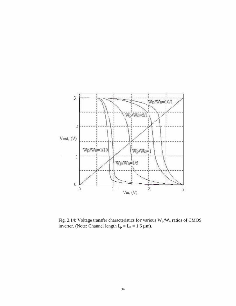
2.5 Variable Threshold Voltage
In general, logic circuits need different switching voltage values for Φt for
better performance. This is obtained by varying the W/L ratio of either the nMOS or
the pMOS transistor [38]. The voltage transfer characteristics of MIFG CMOS
inverter with varying Wp/Wn ratios and a constant L are shown in Fig. 2.14. When
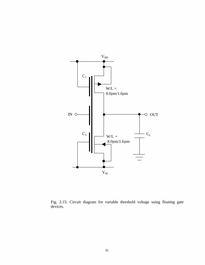
the switching point needs to be shifted by more than 0.6 V, circuits can be designed
easily as shown in Fig. 2.15. Input to capacitor C1 is logic HIGH (3 V) and input to
capacitor C3 is logic LOW (0 V). The values of capacitors C1 or C3 are calculated
depending on the shift required for the switching point. Either the capacitor C1 or C3
is designed as per the requirement. The voltage transfer characteristics for the circuit
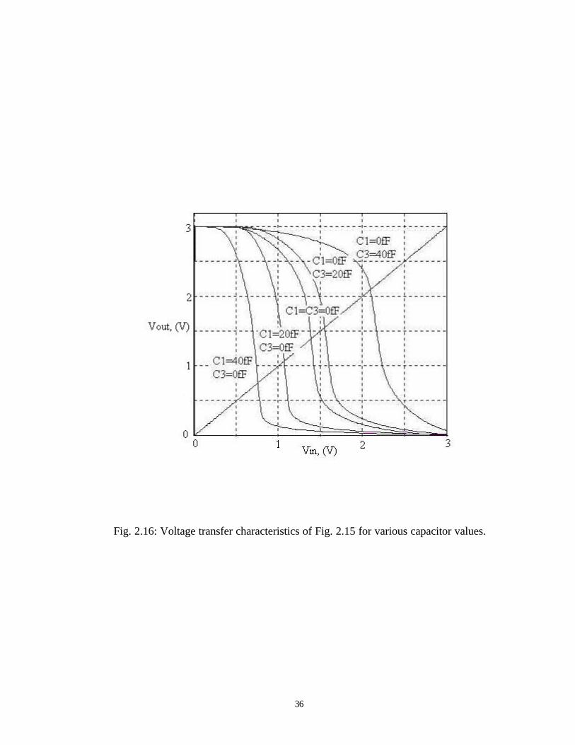
shown in Fig. 2.15 are plotted in Fig. 2.16 with various values of C1 and C3. The
voltage transfer characteristics of MIFG CMOS inverter can be obtained using
SPICE by performing DC analysis. As explained in section 2.3, DC analysis would
open circuit all capacitors and short-circuit all inductors. Such a situation is
overcome by performing transient analysis instead, by using ramp input voltage
source (0 V to 3 V) instead of a DC voltage source at the input of the MIFG
inverter.
2.6 Implementation of MIFG CMOS Transistor
The multiple input floating gate transistors could be implemented in standard
analog CMOS process [39,40]. The following section presents the implementation
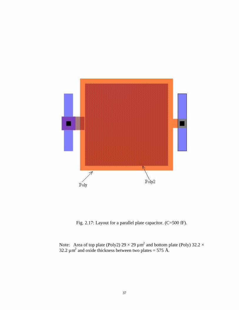
of capacitors for the floating gate MOSFETs. A top view of parallel plate capacitor
is shown in Fig. 2.17. The value of capacitance excluding parasitic capacitances is
given by,
34
Fig. 2.14: Voltage transfer characteristics fo r various Wp/Wn ratios of CMOS inverter. (Note: Channel length Lp = Ln = 1.6 µm).
35
Fig. 2.15: Circuit diagram for variable threshold voltage using floating gate devices.
OUT
CL
VDD
VSS
IN
C3
C1
W/L = 8.0µm/1.6µm
W/L = 8.0µm/1.6µm
36
Fig. 2.16: Voltage transfer characteristics of Fig. 2.15 for various capacitor values.
37
Fig. 2.17: Layout for a parallel plate capacitor. (C=500 fF). Note: Area of top plate (Poly2) 29 × 29 µm2 and bottom plate (Poly) 32.2 × 32.2 µm2 and oxide thickness between two plates = 575 Å.
38
CAC ′= (2.10)
where A is the total area of top plate and C′ is capacitance per unit area. The
insulator between the parallel plates of the capacitor in standard CMOS process is
usually thicker than transistor gate oxide. For a typical 1.5 µm technology CMOS
process, the gate oxide thickness is 300 Å and the oxide thickness between parallel
poly Si plates it is 575 Å. To obtain a capacitor of 500 fF, the area of top plate 29 ×
29 µm2 and that of bottom plate of 32.2 × 32.2 µm2 is used.
There are several ways in which capacitors can be implemented [41]. A
popular one uses double-polysilicon technology in which two poly levels are
available. The top plate and the bottom plate of the capacitor are made of
polysilicon. In a single polysilicon technology, the top plate of the capacitor is made
of metal. A high quality thin oxide is formed as insulator before the top plate is
formed.
Two parasitic capacitances are associated with the main capacitor as shown
in Fig. 2.18. The main one Cp1 is between the bottom plate and the substrate. It
contributes most to the parasitic capacitance. The capacitance due to wiring of the
bottom plate augments this capacitance. The metal wiring used to contact the top
plate results in second small parasitic capacitance Cp2. Another parasitic shown in
Fig. 2.18 by a broken line is resistance Rp of the polysilicon plate. This parasitic is
ignored except at high frequencies. The capacitor of Fig. 2.17 is susceptible to
interference. Any noise signal on substrate can be coupled to the capacitor through
the parasitic capacitances. Also, any voltage variation on the bottom plate of the
capacitor can be coupled to the substrate and through that to other components on
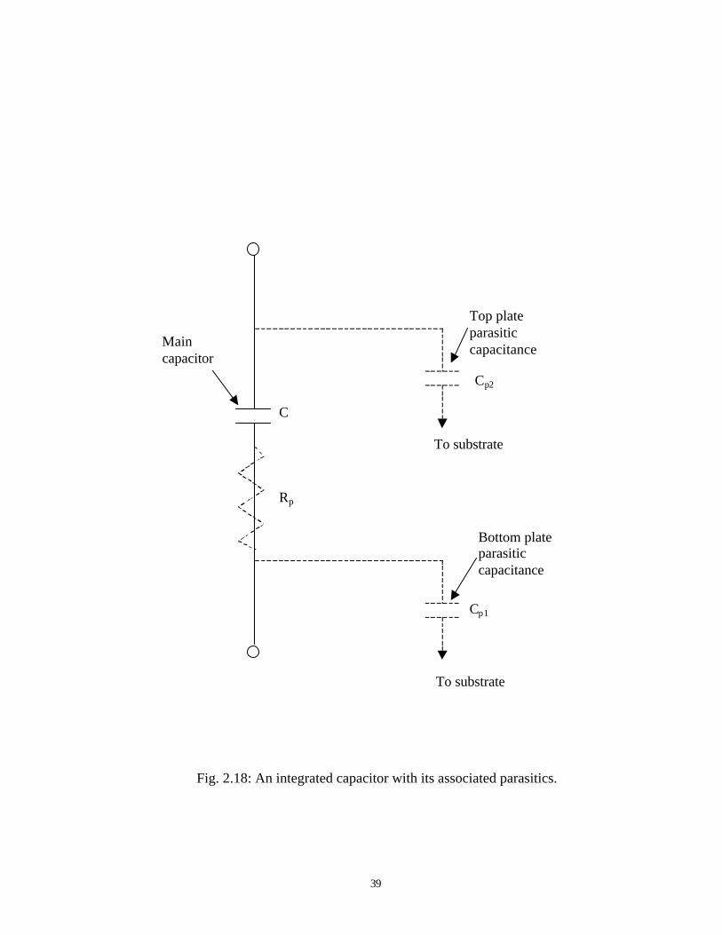
39
Fig. 2.18: An integrated capacitor with its associated parasitics.
Main capacitor
To substrate
Top plate parasitic capacitance
Bottom plate parasitic capacitance
To substrate
C
Cp2
Cp1
Rp
40
the chip. Hence if the capacitor is too large, then it should be shielded from the
substrate by an n-well under it, which is connected to a DC potential (VDD).
2.7 Unit Capacitance
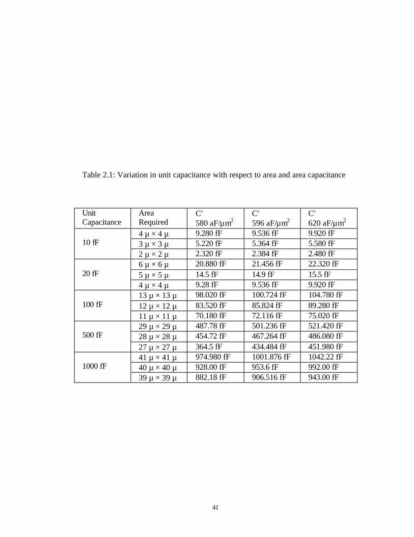
Due to shortcomings in fabrication process, the edges of capacitor plates are
shorter than intended. To maintain constant capacitor ratio, unit size capacitors are
used as explained in reference [41]. An important step in designing floating gate
circuits is setting the value of unit capacitance. As stated earlier, the shorter edges
and variation in thickness of oxide between the plates would change the value of the
capacitance. The MOSIS provides the area capacitance C′ values between the poly
and poly2 layer, which varies from 580 aF/µm2 to 620 aF/µm2 for different runs. An
average value of 596 aF/µm2, which was observed in most of the runs, is used in the
present work. Table 2.1 shows required area for different values of unit capacitance.
The table provides minimum and maximum capacitance values obtained for
variation in area capacitance C′. The table also includes the value of the capacitance
with edges shorted by 0.5 µm and 1.0 µm on each side. The percentage change from
the desired capacitance to worst-case variation in the capacitance is calculated.
For 10 fF %76100536.9
32.2536.9% =×
−=change
For 20 fF %57100456.21
28.9456.21% =×
−=change
For 100 fF %30100724.100
18.70724.100% =×
−=change
For 500 fF %27100236.501
5.364236.501% =×
−=change
41
Table 2.1: Variation in unit capacitance with respect to area and area capacitance Unit Capacitance
Area Required
C′ 580 aF/µm2
C′ 596 aF/µm2
C′ 620 aF/µm2
4 µ × 4 µ 9.280 fF 9.536 fF 9.920 fF 3 µ × 3 µ 5.220 fF 5.364 fF 5.580 fF
10 fF
2 µ × 2 µ 2.320 fF 2.384 fF 2.480 fF 6 µ × 6 µ 20.880 fF 21.456 fF 22.320 fF 5 µ × 5 µ 14.5 fF 14.9 fF 15.5 fF
20 fF
4 µ × 4 µ 9.28 fF 9.536 fF 9.920 fF 13 µ × 13 µ 98.020 fF 100.724 fF 104.780 fF 12 µ × 12 µ 83.520 fF 85.824 fF 89.280 fF
100 fF
11 µ × 11 µ 70.180 fF 72.116 fF 75.020 fF 29 µ × 29 µ 487.78 fF 501.236 fF 521.420 fF 28 µ × 28 µ 454.72 fF 467.264 fF 486.080 fF
500 fF
27 µ × 27 µ 364.5 fF 434.484 fF 451.980 fF 41 µ × 41 µ 974.980 fF 1001.876 fF 1042.22 fF 40 µ × 40 µ 928.00 fF 953.6 fF 992.00 fF
1000 fF
39 µ × 39 µ 882.18 fF 906.516 fF 943.00 fF
42
For 1000 fF %12100876.1001
18.882876.1001% =×
−=change
Since designing floating circuits is based on capacitor ratios, variation in
capacitor values does not affect the functionality of the circuit, so long as the unit
capacitance is large compared to the gate oxide capacitance. Hence unit capacitance
of 500 fF is used in the present work. The circuits should be re-simulated with
worst-case value of unit capacitance to ensure that variation in the value wouldn’t
affect the functionality of the circuit. The parasitic capacitance Cp1 associated with
unit capacitor of 500 fF, explained in previous section is found to be 40 fF. If ‘C’ is
the unit capacitance and input capacitors are multiples of ‘C’ then the value of Cp
used in the equation (2.9) is given by,
1pp CkC ×= (2.11)
where k is given by
....321
CCCCC
k n++++= (2.12)
2.8 Design Issues
Floating gate CMOS inverter, on the other hand has degraded output for a
particular set of inputs, when the calculated sum of input voltages on the floating
gates lies between Φg0 and Φs1. Hence the need for generation of output signal using
a CMOS inverter at the end of the circuit. Consider an MIFG inverter with W/L =
8.0 µm/1.6 µm with supply voltage of 3 V and three input capacitors of 500 fF each.
When inputs to the three capacitors are logic LOW (0 V) and logic HIGH (3 V), the
voltage on floating gate using equation (2.9) is 0 V and 2.75 V, respectively for
value of C0 approximated at 30 fF. A full output swing of 3 V and 0 V is expected at
43
the output. When one of the three inputs is logic HIGH or two of the three inputs are
logic HIGH then the voltage on floating gate given by equation (2.9) is 0.94 V and
1.85 V, respectively. In these cases, a full swing of the output is not expected.
Hence the output needs to be buffered to generate full logic voltage swing.
Initial charge present on the floating gate due to reasons like fabrication may
shift the threshold condition and would result in logical error of the circuit. The
initial charge on the floating gate is to be erased by UV radiation or by using
additional devices for resetting the charge. An nMOS transistor is connected
between the floating gate and ground, to eliminate the charge present on the floating
gate in reset phase. Kotani et.al. [42] proposed a new technique to balance the
charge on the floating gate by connecting the floating ga te to the inverter output.
Simulation of floating gate devices with standard CMOS models provided
by the manufacturer requires, new simulation techniques. The major problem of
simulating floating-gate devices is the inability of the simulator to converge floating
nodes. To avoid the problem of floating nodes at the gate of a transistor, different
approaches have been reported in reference [43-46]. These techniques include use of
additional networks like resistors and voltage controlled voltage sources (VCVS) for
establishing initial floating-gate voltage value. These simulation techniques are
explained in Appendix C.
44
Chapter 3
Conversion from Ternary Logic to Binary Logic
3.1 Overview
The balanced ternary logic is expressed as (-1,0,1). In a standard 3 V CMOS
process, the logic -1, 0, 1 is defined as -3 V, 0 V, 3 V, respectively. The benefits of
using ternary logic system are explained in Chapter 1. In spite of these benefits
ternary logic system has not gained importance in the area of integrated circuit
design. This is due to lack of efficient interfacing circuits with binary logic. Hence
an attempt to design an interface circuit from ternary logic to binary logic has been
made. The circuits are designed using multiple- input floating gate MOS transistors.
The basic structure and operation of floating gate MOSFETs is explained in Chapter
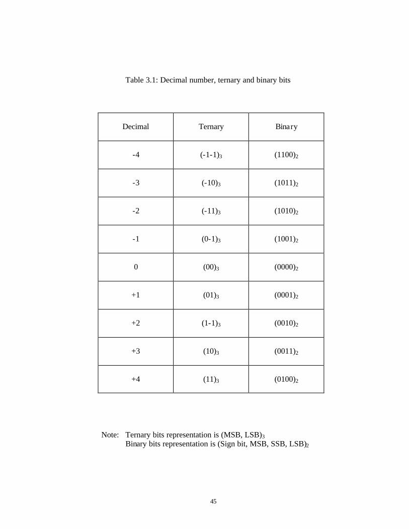
2. Table 3.1 provides ternary logic with corresponding binary bits. The
corresponding decimal number is also included in the table. The representation of
ternary and binary bits for corresponding decimal number is explained using an
example.
Consider a decimal number “-2”, for which the corresponding binary bits are
(1010)2. The left most bit is the sign bit, which is “1” represents the number is
negative and next three bits “010” represents “2”. For decimal number “-2”, the
corresponding ternary bits are (-1,1)3. The conversion from ternary logic to decimal
number is given by,
(-1×31) + (1×30) = (-3) + (1) = -2.
The remaining ternary and binary bit representing corresponding decimal
number is obtained.
45
Table 3.1: Decimal number, ternary and binary bits
Decimal
Ternary
Binary
-4
(-1-1)3
(1100)2
-3
(-10)3
(1011)2
-2
(-11)3
(1010)2
-1
(0-1)3
(1001)2
0
(00)3
(0000)2
+1
(01)3
(0001)2
+2
(1-1)3
(0010)2
+3
(10)3
(0011)2
+4
(11)3
(0100)2
Note: Ternary bits representation is (MSB, LSB)3 Binary bits representation is (Sign bit, MSB, SSB, LSB)2
46
The chapter explains design for the conversion circuits from ternary logic to
binary logic. The circuit block has two ternary logic inputs, a MSB and a LSB and
four binary logic outputs, a sign bit (SB), a most significant bit (MSB), a second
significant bit (SSB) and a least significant bit (LSB). The design of SB, MSB, SSB
and LSB are explained in separate sections. The design of pre- input gate inverter
stages needed to control the main inverter stage is explained in respective
subsections.
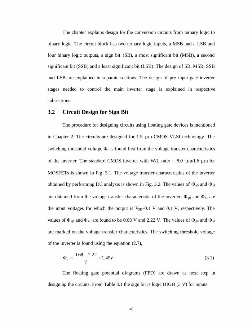
3.2 Circuit Design for Sign Bit
The procedure for designing circuits using floating gate devices is mentioned
in Chapter 2. The circuits are designed for 1.5 µm CMOS VLSI technology. The
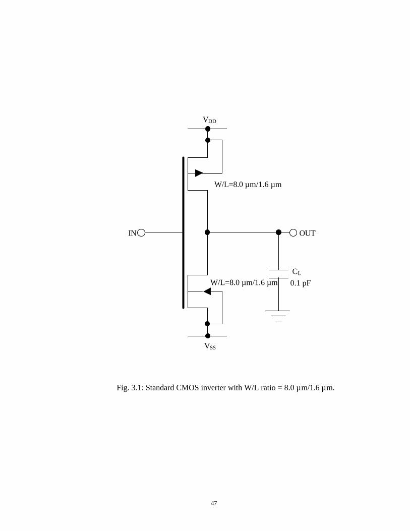
switching threshold voltage Φt is found first from the voltage transfer characteristics
of the inverter. The standard CMOS inverter with W/L ratio = 8.0 µm/1.6 µm for
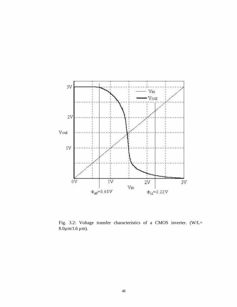
MOSFETs is shown in Fig. 3.1. The voltage transfer characteristics of the inverter
obtained by performing DC analysis is shown in Fig. 3.2. The values of Φg0 and Φs1
are obtained from the voltage transfer characteristic of the inverter. Φg0 and Φs1 are
the input voltages for which the output is VDD-0.1 V and 0.1 V, respectively. The
values of Φg0 and Φs1 are found to be 0.68 V and 2.22 V. The values of Φg0 and Φs1
are marked on the voltage transfer characteristics. The switching threshold voltage
of the inverter is found using the equation (2.7),
.45.12
22.268.0Vt =
+=Φ (3.1)
The floating gate potential diagrams (FPD) are drawn as next step in
designing the circuits. From Table 3.1 the sign bit is logic HIGH (3 V) for inputs
47
Fig. 3.1: Standard CMOS inverter with W/L ratio = 8.0 µm/1.6 µm.
IN OUT
CL
0.1 pF
VDD
VSS
W/L=8.0 µm/1.6 µm
W/L=8.0 µm/1.6 µm
48
Fig. 3.2: Voltage transfer characteristics of a CMOS inverter. (W/L= 8.0µm/1.6 µm).
49
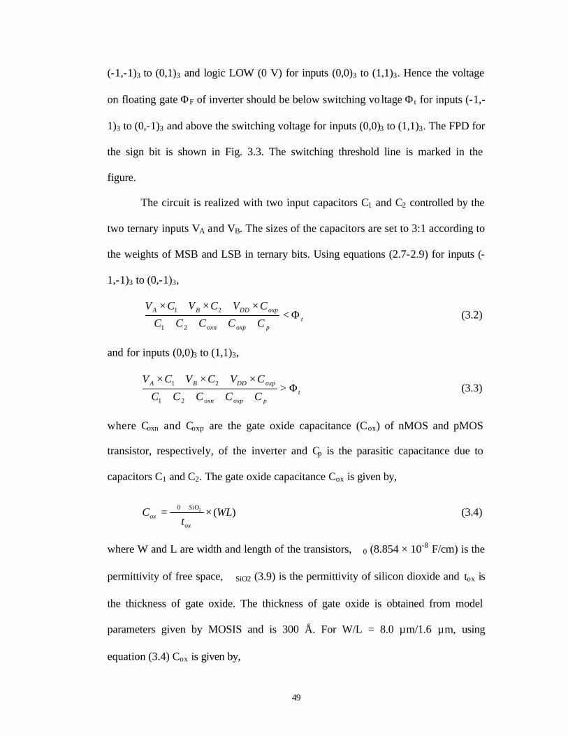
(-1,-1)3 to (0,1)3 and logic LOW (0 V) for inputs (0,0)3 to (1,1)3. Hence the voltage
on floating gate ΦF of inverter should be below switching vo ltage Φt for inputs (-1,-
1)3 to (0,-1)3 and above the switching voltage for inputs (0,0)3 to (1,1)3. The FPD for
the sign bit is shown in Fig. 3.3. The switching threshold line is marked in the
figure.
The circuit is realized with two input capacitors C1 and C2 controlled by the
two ternary inputs VA and VB. The sizes of the capacitors are set to 3:1 according to
the weights of MSB and LSB in ternary bits. Using equations (2.7-2.9) for inputs (-
1,-1)3 to (0,-1)3,
tpoxpoxn
oxpDDBA
CCCCC
CVCVCVΦ<
++++
×+×+×
21
21 (3.2)
and for inputs (0,0)3 to (1,1)3,
tpoxpoxn
oxpDDBA
CCCCC
CVCVCVΦ>
++++
×+×+×
21
21 (3.3)
where Coxn and Coxp are the gate oxide capacitance (Cox) of nMOS and pMOS
transistor, respectively, of the inverter and Cp is the parasitic capacitance due to
capacitors C1 and C2. The gate oxide capacitance Cox is given by,
)(20 WLt
Cox
SiOox ×
∈∈= (3.4)
where W and L are width and length of the transistors, ∈0 (8.854 × 10⁻⁸ F/cm) is the
permittivity of free space, ∈SiO2 (3.9) is the permittivity of silicon dioxide and tox is
the thickness of gate oxide. The thickness of gate oxide is obtained from model
parameters given by MOSIS and is 300 Å. For W/L = 8.0 µm/1.6 µm, using
equation (3.4) Cox is given by,
50
Fig. 3.3: Floating gate potential diagram for the sign bit. (Note: Figure is not drawn to scale).
Principal-Gate Input (Vp)
(1-1)3 (10)3 (11)3 (01)3 (00)3 (0-1)3 (-11)3 (-10)3 (-1-1)3
ΦF, V
Φt
γVDD
51
.1510300
/854.89.36.10.88
fFcm
cmFmmCox ≈
××××
=−
µµ (3.5)
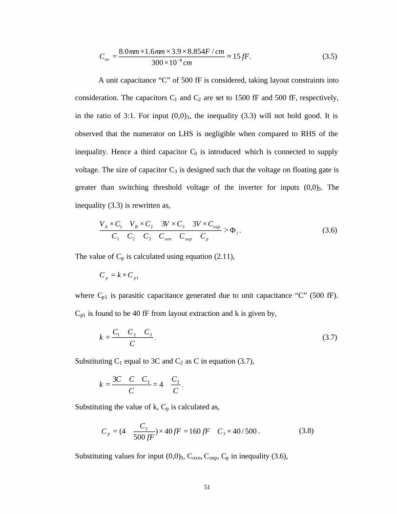
A unit capacitance “C” of 500 fF is considered, taking layout constraints into
consideration. The capacitors C1 and C2 are set to 1500 fF and 500 fF, respectively,
in the ratio of 3:1. For input (0,0)3, the inequality (3.3) will not hold good. It is
observed that the numerator on LHS is negligible when compared to RHS of the
inequality. Hence a third capacitor C3 is introduced which is connected to supply
voltage. The size of capacitor C3 is designed such that the voltage on floating gate is
greater than switching threshold voltage of the inverter for inputs (0,0)3. The
inequality (3.3) is rewritten as,
.33
321
321t
poxpoxn
oxpBA
CCCCCC
CVCVCVCVΦ>
+++++
×+×+×+× (3.6)
The value of Cp is calculated using equation (2.11),
1pp CkC ×=
where Cp1 is parasitic capacitance generated due to unit capacitance “C” (500 fF).
Cp1 is found to be 40 fF from layout extraction and k is given by,
C
CCCk 321 ++
= . (3.7)
Substituting C1 equal to 3C and C2 as C in equation (3.7),
CC
CCCC
k 33 43
+=++
= .
Substituting the value of k, Cp is calculated as,
500/4016040)500
4( 33 ×+=×+= CfFfFfF
CC p . (3.8)
Substituting values for input (0,0)3, Coxn, Coxp, Cp in inequality (3.6),
52
).45.1()500/40160(15155001500
)15(33)500(0)1500(0
33
3 VCfFfFfFCfFfF
fFVCVfFVfFVt
CP
Φ>×++++++
×+×+×+×
4444 34444 21 (3.9)
The smallest value of C3 that satisfies the inequality (3.9) is found to be
3000 fF, which is a multiple of 500 fF (unit capacitance). Substituting the value of
C3 in equation (3.8) value of Cp is found to be 400 fF.
To verify the design, the capacitor values are substituted for input (0,-1)3,
).45.1()240160(151530005001500)15(330003)500()3()1500(0
VfFfFfFfFfFfFfFfFVfFVfFVfFV
tΦ<++++++
+×+×−+× (3.10)
The voltage on floating gate ΦF for ternary inputs is calculated and tabulated
in Table 3.2. The voltage on floating gate ΦF from table is found to be less than
switching threshold voltage for inputs (-1,-1)3 to (0,-1)3 and greater than switching
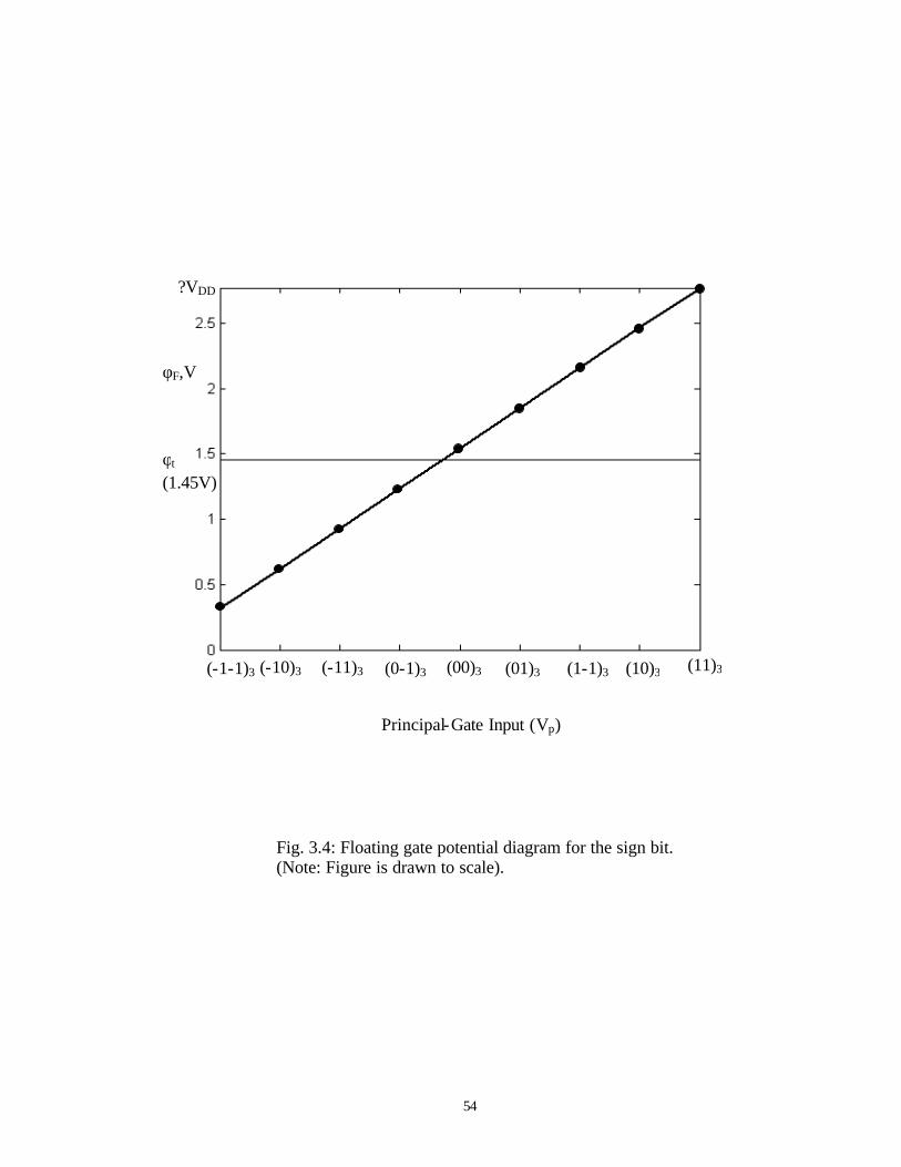
threshold voltage for inputs (0,0)3 to (1,1)3. The FPD for the SB to scale is shown in
Fig. 3.4. The circuit diagram for sign bit is shown in Fig. 3.5.
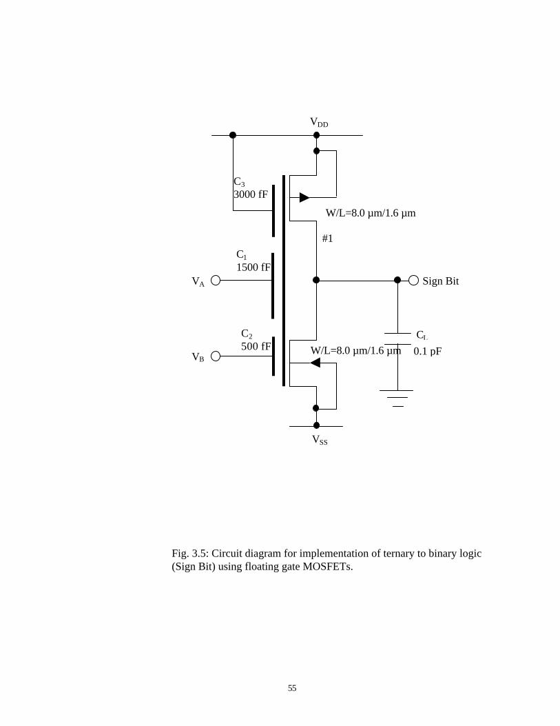
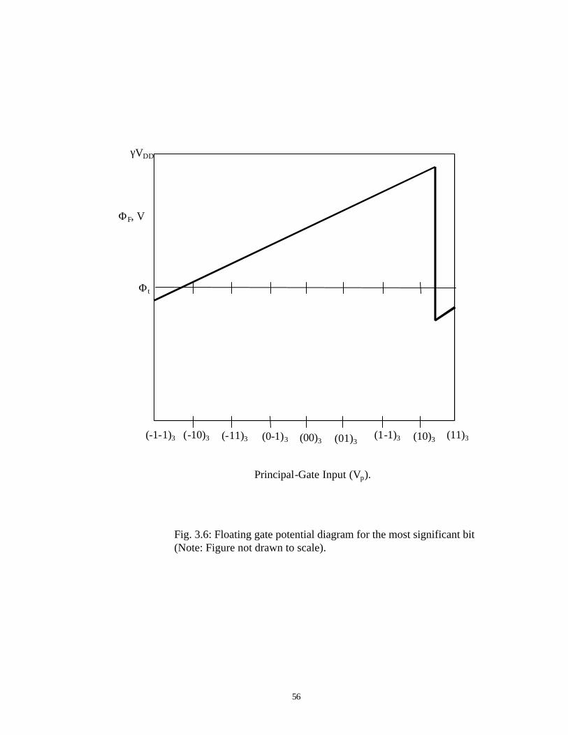
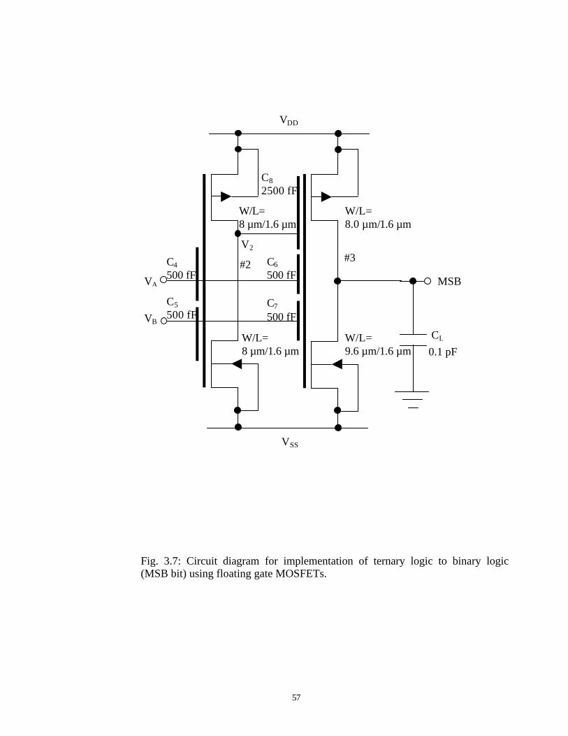
3.3 Circuit Design for MSB
The most significant bit is found to be logic HIGH (3V) for inputs (-1,-1)3
and (1,1)3 and logic LOW (0 V) for rest of inputs from Table 3.1. The FPD for the
MSB is shown in Fig. 3.6. The potential on floating gate is below switching
threshold voltage Φt for inputs (-1,-1)3, (1,1)3 and above switching threshold voltage
for inputs (-1,0)3 to (1,0)3. Voltage on floating gate falls below switching threshold
voltage once, hence one pre-input gate inverter stage is required to control voltage
on floating gate. Figure 3.7 shows circuit level implementation for MSB. In Fig. 3.7,
the main inverter stage (#3) has three input capacitors C6, C7 and C8. The capacitors
C6 and C7 are controlled by ternary inputs VA and VB, respectively and capacitor C8
53
Table 3.2: Voltage on the floating gate ΦF for the sign bit for corresponding ternary inputs (Φt for the MIFG inverter is 1.45 V)
Ternary Inputs
Voltage on Floating
Gate ΦF
(-1-1)3
0.316
ΦF < Φt
(-10)3
0.623
ΦF < Φt
(-11)3
0.929
ΦF < Φt
(0-1)3
1.236
ΦF < Φt
(00)3
1.543
ΦF > Φt
(01)3
1.849
ΦF > Φt
(1-1)3
2.156
ΦF > Φt
(10)3
2.463
ΦF > Φt
(11)3
2.769
ΦF > Φt
54
Fig. 3.4: Floating gate potential diagram for the sign bit. (Note: Figure is drawn to scale).
φF,V
(-1-1)3 (-10)3 (-11)3 (0-1)3 (00)3 (01)3 (1-1)3 (10)3 (11)3
φt (1.45V)
?VDD
Principal-Gate Input (Vp)
55
Fig. 3.5: Circuit diagram for implementation of ternary to binary logic (Sign Bit) using floating gate MOSFETs.
VA Sign Bit
CL
0.1 pF
VDD
VSS
W/L=8.0 µm/1.6 µm
W/L=8.0 µm/1.6 µm
C1 1500 fF
#1
C2 500 fF
C3 3000 fF
VB
56
Fig. 3.6: Floating gate potential diagram for the most significant bit (Note: Figure not drawn to scale).
Principal-Gate Input (Vp).
(1-1)3 (10)3 (11)3 (01)3 (00)3 (0-1)3 (-11)3 (-10)3 (-1-1)3
ΦF, V
Φt
γVDD
57
Fig. 3.7: Circuit diagram for implementation of ternary logic to binary logic (MSB bit) using floating gate MOSFETs.
VA MSB
CL
0.1 pF
VDD
VSS
W/L= 8 µm/1.6 µm
W/L= 8 µm/1.6 µm
C4 500 fF
#2
W/L= 8.0 µm/1.6 µm
W/L= 9.6 µm/1.6 µm
#3C6 500 fF
C8 2500 fF
C7 500 fF VB
C5 500 fF
V2
58
is controlled by the output V2 of pre- input gate inverter stage (#2). Using equations
(2.7-2.9), the inequalities for the MSB can be written as follows. For input (-1,-1)3,
)45.1(3)3()3(
876
8276 VCCCCCC
CVCVCVCVt
poxpoxn
oxp Φ<+++++
×+×+×−+×− (3.11)
and for (1,1)3,
)45.1(3)3()3(
876
8276 VCCCCCC
CVCVCVCVt
poxpoxn
oxp Φ<+++++
×+×+×+×. (3.12)
The inequality (3.10) can be satisfied only if V2 is LOW (0 V) for input
(1,1)3. Hence the output of pre-input inverter stage (#2) is LOW (0 V) for input
(1,1)3 and HIGH (3 V) for rest of the inputs. For inputs (-1,0)3 to (1,0)3, voltage on
floating gate should be greater than switching threshold voltage. Considering the
extreme input (-1,0)3, the inequality is given by,
)45.1()3()3()0()3(
876
876 VCCCCCC
CVCVCVCVt
poxpoxn
oxp Φ>+++++
×+×+×+×−. (3.13)
The sizes of capacitors C6 and C7 is set to 3:1 in the ratio of MSB and LSB
as in ternary bits. The minimum size of the capacitance of C6 and C7 is 1500 fF and
500fF, respectively.
The value of Cp is obtained from equation (2.11), where Cp1 = 40 fF and k is
given by,
C
CCCk 876 ++
= . (3.14)
Substituting C6 equal to 3C, C7 equal to C in equation (3.14),
CC
CCCC
k 88 43
+=++
= .
Substituting the value of k, Cp is calculated as,
59
500/4016040)500
4( 88 ×+=×+= CfFfFfF
CC p .
Substituting the values for input (-1,0)3, Coxn, Coxp, Cp in inequality (3.13),
)45.1.()500/40160(15155001500
)15(33)500()0()1500()3(
88
8 VCfFfFfFCfFfF
fFVCVfFVfFVt
CP
Φ>×++++++×+×+×+×−
4444 34444 21 (3.15)
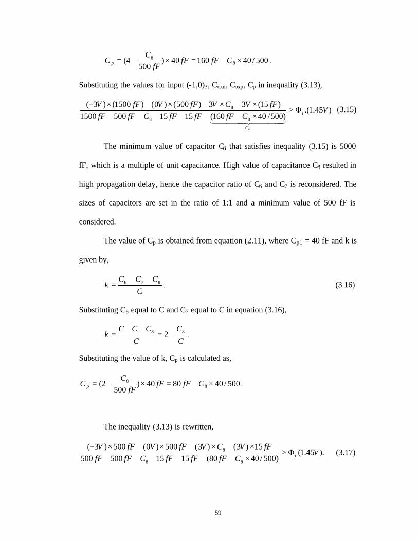
The minimum value of capacitor C8 that satisfies inequality (3.15) is 5000
fF, which is a multiple of unit capacitance. High value of capacitance C8 resulted in
high propagation delay, hence the capacitor ratio of C6 and C7 is reconsidered. The
sizes of capacitors are set in the ratio of 1:1 and a minimum value of 500 fF is
considered.
The value of Cp is obtained from equation (2.11), where Cp1 = 40 fF and k is
given by,
C
CCCk 876 ++
= . (3.16)
Substituting C6 equal to C and C7 equal to C in equation (3.16),
CC
CCCC
k 88 2 +=++
= .
Substituting the value of k, Cp is calculated as,
500/408040)500
2( 88 ×+=×+= CfFfFfF
CC p .
The inequality (3.13) is rewritten,
).45.1()500/4080(1515500500
15)3()3(500)0(500)3(
88
8 VCfFfFfFCfFfF
fFVCVfFVfFVtΦ>
×++++++×+×+×+×−
(3.17)
60
The minimum value of capacitor C8 that satisfies the inequality (3.17) is
2500 fF. Substituting the value of C8, the value of Cp is found to be 280 fF.
The voltage on floating gate ΦF of the main inverter stage (#3) of MSB, for
ternary inputs is calculated and tabulated in Table 3.3. The voltage on floating gate
ΦF is less than switching threshold voltage for inputs (-1,-1)3 and (1,1)3 and greater
than switching threshold voltage for inputs (-1,0)3 to (1,0)3 satisfying the conditions.
The FPD for the MSB to scale is shown in Fig. 3.8. The FPD shown in Fig. 3.8 is
different when compared to Fig. 3.6, as the capacitor ratio of C6 to C7 is set to 1:1,
instead of 3:1.
3.3.1 Circuit Design for #2 Stage
The output of stage #2 is LOW (0 V) for input (1,1)3 and HIGH(3V) for test
of the inputs. The circuit can be realized with two input capacitors C4 and C5. For
input (1,1)3, the inequality is written using equations (2.7-2.9),
)45.1()3()3()3(
54
54 VCCCCC
CVCVCVt
poxpoxn
oxp Φ>++++
×+×+×. (3.18)
The capacitors C4 and C5 are equal and minimum size unit capacitors (500
fF) satisfy the inequality (3.18). The voltage on the floating gate ΦF is calculated
and tabulated in Table 3.4. The output of stage (#2) is buffered which controls the
capacitor C8 of the main inverter stage. The transistor widths used in buffer are
Wp/Wn = 16 µm/16 µm and Wp/Wn = 40 µm/40 µm. The circuit diagram for most
significant bit is shown in Fig. 3.7. The non- inverting buffer at the output of #2
stage is not shown in the figure.
61
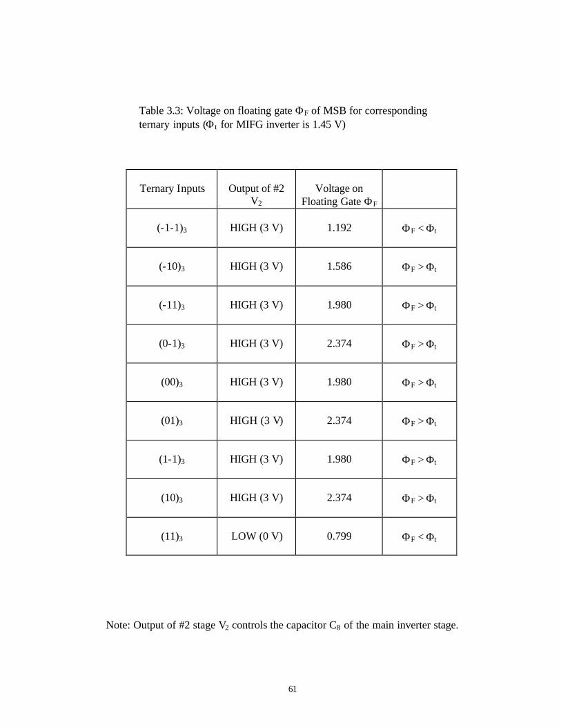
Table 3.3: Voltage on floating gate ΦF of MSB for corresponding ternary inputs (Φt for MIFG inverter is 1.45 V)
Ternary Inputs
Output of #2
V2
Voltage on
Floating Gate ΦF
(-1-1)3
HIGH (3 V)
1.192
ΦF < Φt
(-10)3
HIGH (3 V)
1.586
ΦF > Φt
(-11)3
HIGH (3 V)
1.980
ΦF > Φt
(0-1)3
HIGH (3 V)
2.374
ΦF > Φt
(00)3
HIGH (3 V)
1.980
ΦF > Φt
(01)3
HIGH (3 V)
2.374
ΦF > Φt
(1-1)3
HIGH (3 V)
1.980
ΦF > Φt
(10)3
HIGH (3 V)
2.374
ΦF > Φt
(11)3
LOW (0 V)
0.799
ΦF < Φt
Note: Output of #2 stage V2 controls the capacitor C8 of the main inverter stage.
62
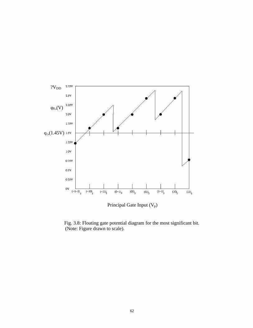
Fig. 3.8: Floating gate potential diagram for the most significant bit. (Note: Figure drawn to scale).
φF,(V)
φt,(1.45V)
?VDD
Principal Gate Input (Vp)
63
Table 3.4: Voltage on floating gate ΦF of V2 for corresponding ternary inputs (Φt for MIFG inverter is 1.45 V)
Ternary Inputs
Voltage on Floating
Gate ΦF
(-1-1)3
-2.662
ΦF < Φt
(-10)3
-1.310
ΦF < Φt
(-11)3
0.004
ΦF < Φt
(0-1)3
-1.310
ΦF < Φt
(00)3
0.004
ΦF < Φt
(01)3
0.490
ΦF < Φt
(1-1)3
0.004
ΦF < Φt
(10)3
0.490
ΦF < Φt
(11)3
2.743
ΦF > Φt
64
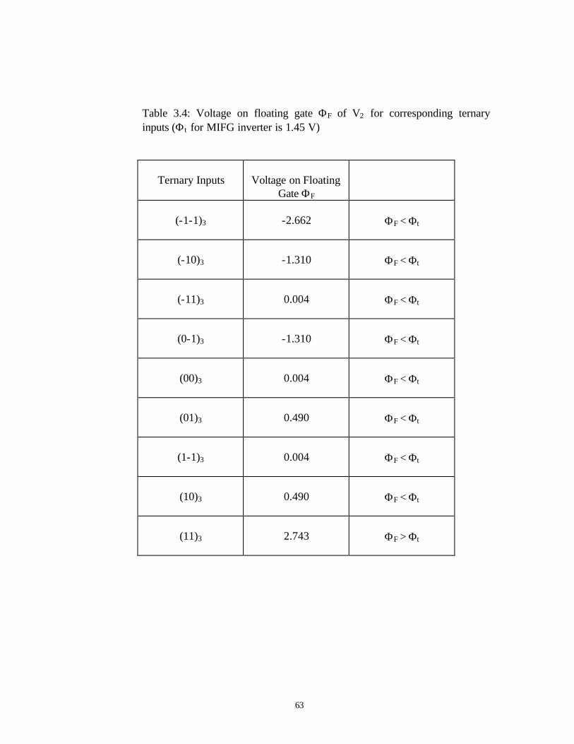
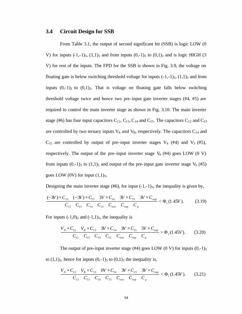
3.4 Circuit Design for SSB
From Table 3.1, the output of second significant bit (SSB) is logic LOW (0
V) for inputs (-1,-1)3, (1,1)3 and from inputs (0,-1)3 to (0,1)3 and is logic HIGH (3
V) for rest of the inputs. The FPD for the SSB is shown in Fig. 3.9, the voltage on
floating gate is below switching threshold voltage for inputs (-1,-1)3, (1,1)3 and from
inputs (0,-1)3 to (0,1)3. That is voltage on floating gate falls below switching
threshold voltage twice and hence two pre- input gate inverter stages (#4, #5) are
required to control the main inverter stage as shown in Fig. 3.10. The main inverter
stage (#6) has four input capacitors C12, C13, C14 and C15. The capacitors C12 and C13
are controlled by two ternary inputs VA and VB, respectively. The capacitors C14 and
C15 are controlled by output of pre- input inverter stages V4 (#4) and V5 (#5),
respectively. The output of the pre- input inverter stage V4 (#4) goes LOW (0 V)
from inputs (0,-1)3 to (1,1)3 and output of the pre- input gate inverter stage V5 (#5)
goes LOW (0V) for input (1,1)3.
Designing the main inverter stage (#6), for input (-1,-1)3, the inequality is given by,
).45.1(333)3()3(
15141312
15141312 VCCCCCCC
CVCVCVCVCVt
poxpoxn
oxp Φ<++++++
×+×+×+×−+×− (3.19)
For inputs (-1,0)3 and (-1,1)3, the inequality is
).45.1(333
15141312
15141312 VCCCCCCC
CVCVCVCVCVt
poxpoxn
oxpBA Φ>++++++
×+×+×+×+× (3.20)
The output of pre-input inverter stage (#4) goes LOW (0 V) for inputs (0,-1)3
to (1,1)3, hence for inputs (0,-1)3 to (0,1)3 the inequality is,
).45.1(330
15141312
15141312 VCCCCCCC
CVCVCVCVCVt
poxpoxn
oxpBA Φ<++++++
×+×+×+×+× (3.21)
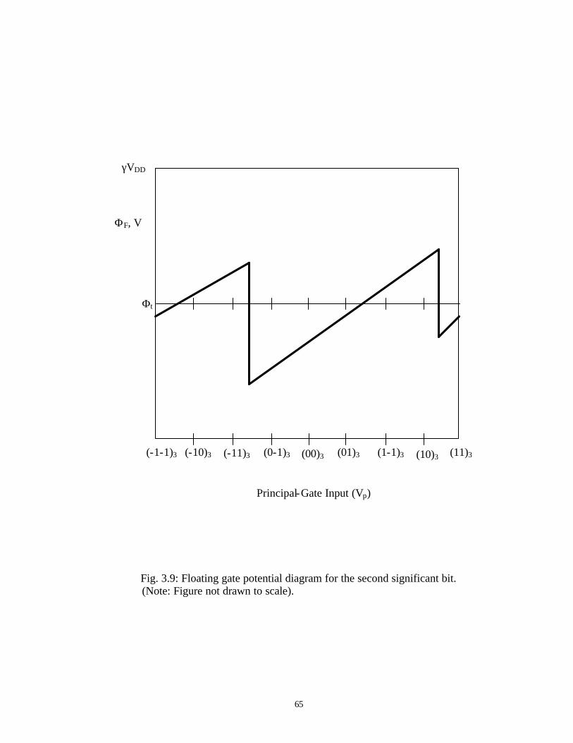
65
Fig. 3.9: Floating gate potential diagram for the second significant bit. (Note: Figure not drawn to scale).
(1-1)3 (10)3 (11)3 (01)3 (00)3 (0-1)3 (-11)3 (-10)3 (-1-1)3
ΦF, V
Φt
Principal-Gate Input (Vp)
γVDD
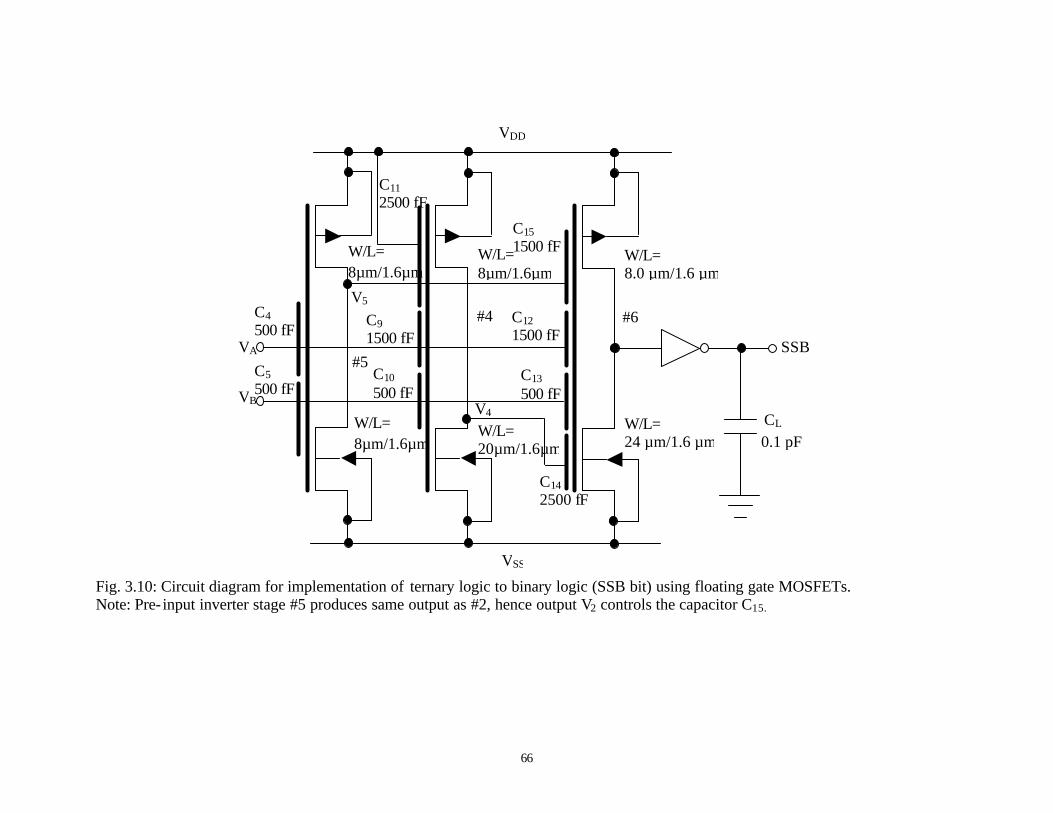
66
Fig. 3.10: Circuit diagram for implementation of ternary logic to binary logic (SSB bit) using floating gate MOSFETs. Note: Pre- input inverter stage #5 produces same output as #2, hence output V2 controls the capacitor C15.
VA SSB
CL 0.1 pF
VDD
VSS
W/L= 8µm/1.6µm
W/L= 8µm/1.6µm
C4 500 fF
#5
W/L= 8µm/1.6µm
W/L= 20µm/1.6µm
#4 C9 1500 fF
C11 2500 fF
C10 500 fF VB
C5 500 fF
W/L= 8.0 µm/1.6 µm
W/L= 24 µm/1.6 µm
#6 C12 1500 fF
C13 500 fF
C14 2500 fF
C15 1500 fF
V5
V4
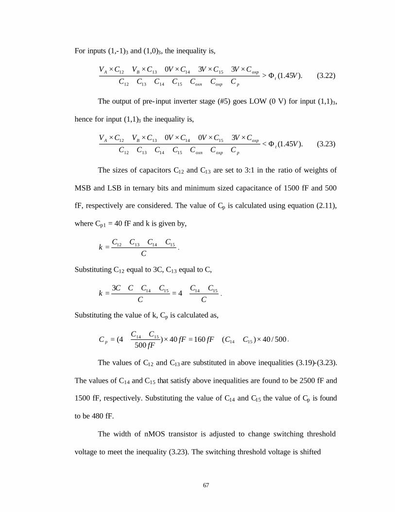
67
For inputs (1,-1)3 and (1,0)3, the inequality is,
).45.1(330
15141312
15141312 VCCCCCCC
CVCVCVCVCVt
poxpoxn
oxpBA Φ>++++++
×+×+×+×+× (3.22)
The output of pre- input inverter stage (#5) goes LOW (0 V) for input (1,1)3,
hence for input (1,1)3 the inequality is,
).45.1(300
15141312
15141312 VCCCCCCC
CVCVCVCVCVt
poxpoxn
oxpBA Φ<++++++
×+×+×+×+× (3.23)
The sizes of capacitors C12 and C13 are set to 3:1 in the ratio of weights of
MSB and LSB in ternary bits and minimum sized capacitance of 1500 fF and 500
fF, respectively are considered. The value of Cp is calculated using equation (2.11),
where Cp1 = 40 fF and k is given by,
C
CCCCk 15141312 +++
= .
Substituting C12 equal to 3C, C13 equal to C,
CCC
CCCCC
k 15141514 43 +
+=+++
= .
Substituting the value of k, Cp is calculated as,
500/40)(16040)500
4( 15141514 ×++=×
++= CCfFfF
fFCC
C p .
The values of C12 and C13 are substituted in above inequalities (3.19)-(3.23).
The values of C14 and C15 that satisfy above inequalities are found to be 2500 fF and
1500 fF, respectively. Substituting the value of C14 and C15 the value of Cp is found
to be 480 fF.
The width of nMOS transistor is adjusted to change switching threshold
voltage to meet the inequality (3.23). The switching threshold voltage is shifted
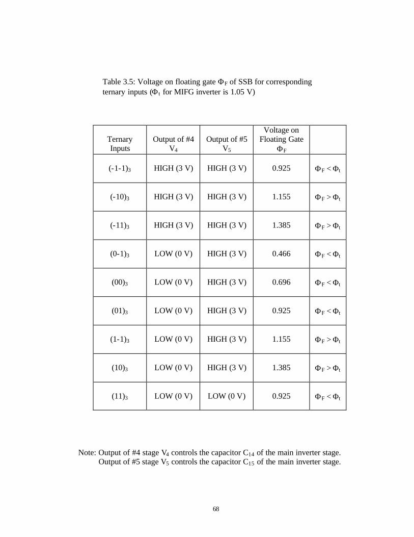
68
Table 3.5: Voltage on floating gate ΦF of SSB for corresponding ternary inputs (Φt for MIFG inverter is 1.05 V)
Ternary Inputs
Output of #4
V4
Output of #5
V5
Voltage on Floating Gate
ΦF
(-1-1)3
HIGH (3 V)
HIGH (3 V)
0.925
ΦF < Φt
(-10)3
HIGH (3 V)
HIGH (3 V)
1.155
ΦF > Φt
(-11)3
HIGH (3 V)
HIGH (3 V)
1.385
ΦF > Φt
(0-1)3
LOW (0 V)
HIGH (3 V)
0.466
ΦF < Φt
(00)3
LOW (0 V)
HIGH (3 V)
0.696
ΦF < Φt
(01)3
LOW (0 V)
HIGH (3 V)
0.925
ΦF < Φt
(1-1)3
LOW (0 V)
HIGH (3 V)
1.155
ΦF > Φt
(10)3
LOW (0 V)
HIGH (3 V)
1.385
ΦF > Φt
(11)3
LOW (0 V)
LOW (0 V)
0.925
ΦF < Φt
Note: Output of #4 stage V4 controls the capacitor C14 of the main inverter stage. Output of #5 stage V5 controls the capacitor C15 of the main inverter stage.
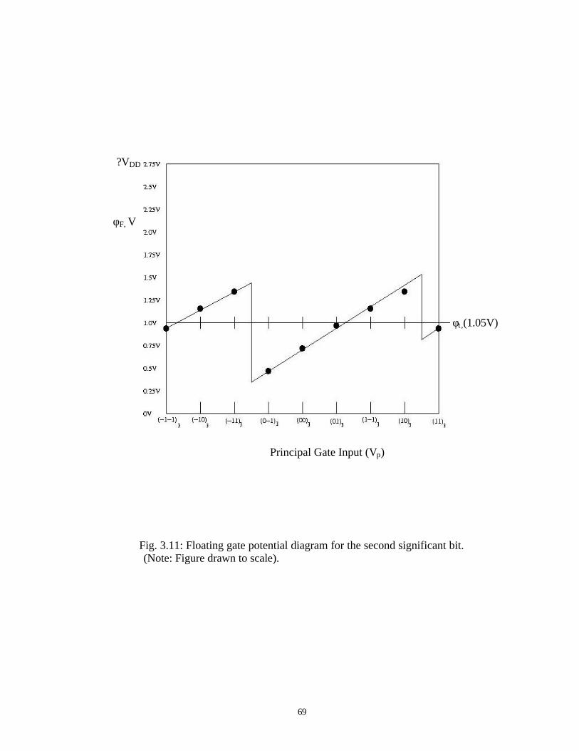
69
Fig. 3.11: Floating gate potential diagram for the second significant bit. (Note: Figure drawn to scale).
φF, V
φt ,(1.05V)
?VDD
Principal Gate Input (Vp)
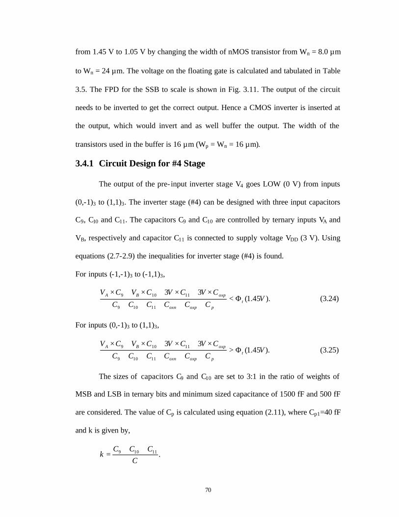
70
from 1.45 V to 1.05 V by changing the width of nMOS transistor from Wn = 8.0 µm
to Wn = 24 µm. The voltage on the floating gate is calculated and tabulated in Table
3.5. The FPD for the SSB to scale is shown in Fig. 3.11. The output of the circuit
needs to be inverted to get the correct output. Hence a CMOS inverter is inserted at
the output, which would invert and as well buffer the output. The width of the
transistors used in the buffer is 16 µm (Wp = Wn = 16 µm).
3.4.1 Circuit Design for #4 Stage
The output of the pre- input inverter stage V4 goes LOW (0 V) from inputs
(0,-1)3 to (1,1)3. The inverter stage (#4) can be designed with three input capacitors
C9, C10 and C11. The capacitors C9 and C10 are controlled by ternary inputs VA and
VB, respectively and capacitor C11 is connected to supply voltage VDD (3 V). Using
equations (2.7-2.9) the inequalities for inverter stage (#4) is found.
For inputs (-1,-1)3 to (-1,1)3,
).45.1(33
11109
11109 VCCCCCC
CVCVCVCVt
poxpoxn
oxpBA Φ<+++++
×+×+×+× (3.24)
For inputs (0,-1)3 to (1,1)3,
).45.1(33
11109
11109 VCCCCCC
CVCVCVCVt
poxpoxn
oxpBA Φ>+++++
×+×+×+× (3.25)
The sizes of capacitors C9 and C10 are set to 3:1 in the ratio of weights of
MSB and LSB in ternary bits and minimum sized capacitance of 1500 fF and 500 fF
are considered. The value of Cp is calculated using equation (2.11), where Cp1=40 fF
and k is given by,
.11109
CCCC
k++
=

71
Substituting C9 equal to 3C, C10 equal to C,
.43 1111
CC
CCCC
k +=++
=
Substituting the value of k, Cp is calculated as,
.500/40)(16040)500
4( 1111 ×+=×+= CfFfFfF
CC p
Substituting the value of C9, C10 and Cp in the inequalities (3.24,3.25) the
minimum value of C11 is 3500 fF, which is a multiple of 500 fF. For better timing
response, the value of C11 can be reduced and still meet the inequalities by
increasing the W/L ratio of nMOS transistor, in other words shifting switching
threshold voltage. The width of nMOS transistor Wn = 20 µm is used and value of
C11 reduces to 2500 fF and is shown in Fig. 3.10. Substituting the value of C9, C10
and C11, the value of Cp is found to be 360 fF.
3.4.2 Circuit Design for #5 Stage
The output of the pre- input gate inverter stage (#5) is same as the output of
pre-input gate inverter stage (#2). Hence the output V2 of (#2) is used to control the
capacitor C15.
3.5 Circuit Design for LSB
The least significant bit is designed on similar lines. The output of the LSB
bit is HIGH (3 V) for odd decimal numbers (-3, -1, 1, 3) and LOW (0 V) for even
decimal numbers (-4, -2, 0, 2, 4). From Table 3.1 the FPD for LSB is drawn and is
shown in Fig. 3.12. From FPD, the voltage on floating gate falls below switching
threshold voltage four times, hence four pre- input gate inverter stages are used to
control the voltage on floating gate as shown in Fig. 3.13. The main inverter stage
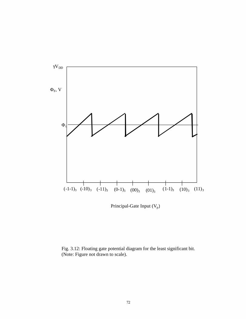
72
Fig. 3.12: Floating gate potential diagram for the least significant bit.
(Note: Figure not drawn to scale).
Principal-Gate Input (Vp)
(1-1)3 (10)3 (11)3(01)3(00)3(0-1)3(-11)3(-10)3(-1-1)3
ΦF, V
Φt
γVDD
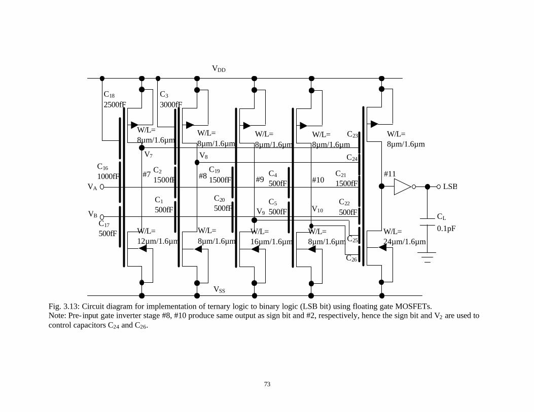
73
Fig. 3.13: Circuit diagram for implementation of ternary logic to binary logic (LSB bit) using floating gate MOSFETs. Note: Pre- input gate inverter stage #8, #10 produce same output as sign bit and #2, respectively, hence the sign bit and V2 are used to control capacitors C24 and C26.
VSS
LSB
CL 0.1pF W/L=
8µm/1.6µm
VA
VDD
W/L= 8µm/1.6µm
W/L= 12µm/1.6µm
C16 1000fF #7
W/L= 8µm/1.6µm
C2 1500fF
C3 3000fF
C1 500fF VB
C17 500fF
W/L= 8µm/1.6µm
W/L= 16µm/1.6µm
#9 C19 1500fF
C20 500fF
C18 2500fF
W/L= 8µm/1.6µm
W/L= 8µm/1.6µm
C4 500fF
C5 500fF
W/L= 8µm/1.6µm
W/L= 24µm/1.6µm
C21 1500fF
C22 500fF
#10
V7
#8
V8
V9 V10
C23
C24
C26
C25
#11
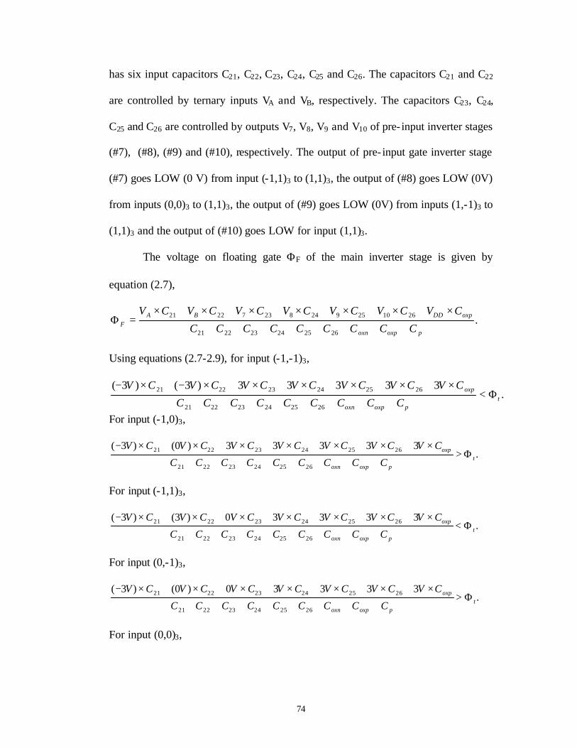
74
has six input capacitors C21, C22, C23, C24, C25 and C26. The capacitors C21 and C22
are controlled by ternary inputs VA and VB, respectively. The capacitors C23, C24,
C25 and C26 are controlled by outputs V7, V8, V9 and V10 of pre- input inverter stages
(#7), (#8), (#9) and (#10), respectively. The output of pre- input gate inverter stage
(#7) goes LOW (0 V) from input (-1,1)3 to (1,1)3, the output of (#8) goes LOW (0V)
from inputs (0,0)3 to (1,1)3, the output of (#9) goes LOW (0V) from inputs (1,-1)3 to
(1,1)3 and the output of (#10) goes LOW for input (1,1)3.
The voltage on floating gate ΦF of the main inverter stage is given by
equation (2.7),
.262524232221
26102592482372221
poxpoxn
oxpDDBAF CCCCCCCCC
CVCVCVCVCVCVCV
++++++++
×+×+×+×+×+×+×=Φ
Using equations (2.7-2.9), for input (-1,-1)3,
.33333)3()3(
262524232221
262524232221t
poxpoxn
oxp
CCCCCCCCC
CVCVCVCVCVCVCVΦ<
++++++++
×+×+×+×+×+×−+×−
For input (-1,0)3,
.33333)0()3(
262524232221
262524232221t
poxpoxn
oxp
CCCCCCCCC
CVCVCVCVCVCVCVΦ>
++++++++
×+×+×+×+×+×+×−
For input (-1,1)3,
.33330)3()3(
262524232221
262524232221t
poxpoxn
oxp
CCCCCCCCC
CVCVCVCVCVCVCVΦ<
++++++++
×+×+×+×+×+×+×−
For input (0,-1)3,
.33330)0()3(
262524232221
262524232221t
poxpoxn
oxp
CCCCCCCCC
CVCVCVCVCVCVCVΦ>
++++++++
×+×+×+×+×+×+×−
For input (0,0)3,
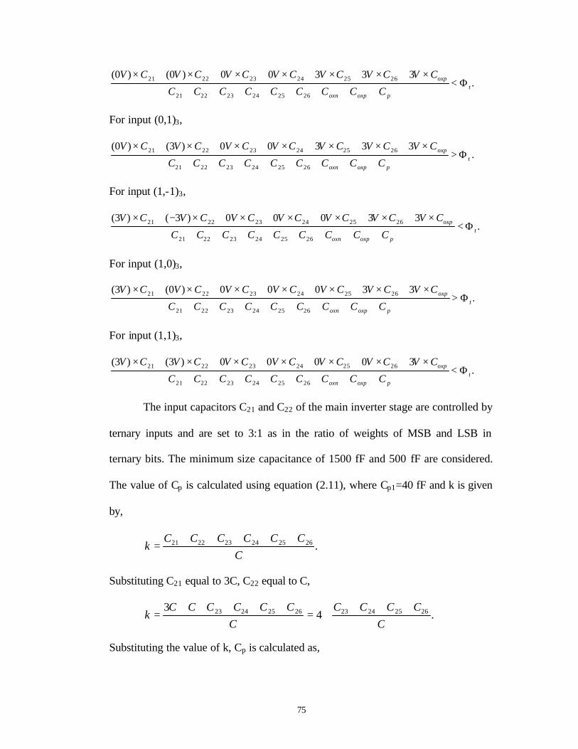
75
.33300)0()0(
262524232221
262524232221t
poxpoxn
oxp
CCCCCCCCC
CVCVCVCVCVCVCVΦ<
++++++++
×+×+×+×+×+×+×
For input (0,1)3,
.33300)3()0(
262524232221
262524232221t
poxpoxn
oxp
CCCCCCCCC
CVCVCVCVCVCVCVΦ>
++++++++
×+×+×+×+×+×+×
For input (1,-1)3,
.33000)3()3(
262524232221
262524232221t
poxpoxn
oxp
CCCCCCCCC
CVCVCVCVCVCVCVΦ<
++++++++
×+×+×+×+×+×−+×
For input (1,0)3,
.33000)0()3(
262524232221
262524232221t
poxpoxn
oxp
CCCCCCCCC
CVCVCVCVCVCVCVΦ>
++++++++
×+×+×+×+×+×+×
For input (1,1)3,
.30000)3()3(
262524232221
262524232221t
poxpoxn
oxp
CCCCCCCCC
CVCVCVCVCVCVCVΦ<
++++++++
×+×+×+×+×+×+×
The input capacitors C21 and C22 of the main inverter stage are controlled by
ternary inputs and are set to 3:1 as in the ratio of weights of MSB and LSB in
ternary bits. The minimum size capacitance of 1500 fF and 500 fF are considered.
The value of Cp is calculated using equation (2.11), where Cp1=40 fF and k is given
by,
.262524232221
CCCCCCC
k+++++
=
Substituting C21 equal to 3C, C22 equal to C,
.43 2625242326252423
CCCCC
CCCCCCC
k+++
+=+++++
=
Substituting the value of k, Cp is calculated as,
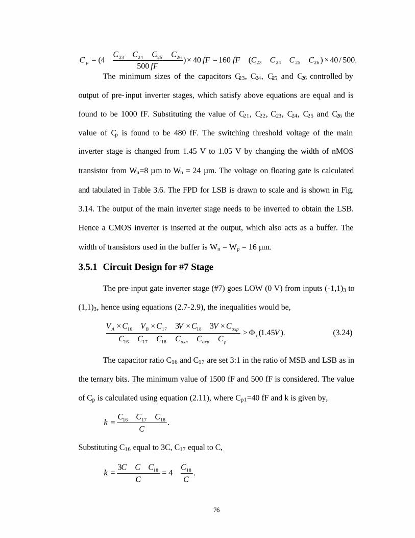
76
.500/40)(16040)500
4( 2625242326252423 ×++++=×
++++= CCCCfFfF
fFCCCC
C p
The minimum sizes of the capacitors C23, C24, C25 and C26 controlled by
output of pre- input inverter stages, which satisfy above equations are equal and is
found to be 1000 fF. Substituting the value of C21, C22, C23, C24, C25 and C26 the
value of Cp is found to be 480 fF. The switching threshold voltage of the main
inverter stage is changed from 1.45 V to 1.05 V by changing the width of nMOS
transistor from Wn=8 µm to Wn = 24 µm. The voltage on floating gate is calculated
and tabulated in Table 3.6. The FPD for LSB is drawn to scale and is shown in Fig.
3.14. The output of the main inverter stage needs to be inverted to obtain the LSB.
Hence a CMOS inverter is inserted at the output, which also acts as a buffer. The
width of transistors used in the buffer is Wn = Wp = 16 µm.
3.5.1 Circuit Design for #7 Stage
The pre-input gate inverter stage (#7) goes LOW (0 V) from inputs (-1,1)3 to
(1,1)3, hence using equations (2.7-2.9), the inequalities would be,
).45.1(33
181716
181716 VCCCCCC
CVCVCVCVt
poxpoxn
oxpBA Φ>+++++
×+×+×+× (3.24)
The capacitor ratio C16 and C17 are set 3:1 in the ratio of MSB and LSB as in
the ternary bits. The minimum value of 1500 fF and 500 fF is considered. The value
of Cp is calculated using equation (2.11), where Cp1=40 fF and k is given by,
.181716
CCCC
k++
=
Substituting C16 equal to 3C, C17 equal to C,
.43 1818
CC
CCCC
k +=++
=
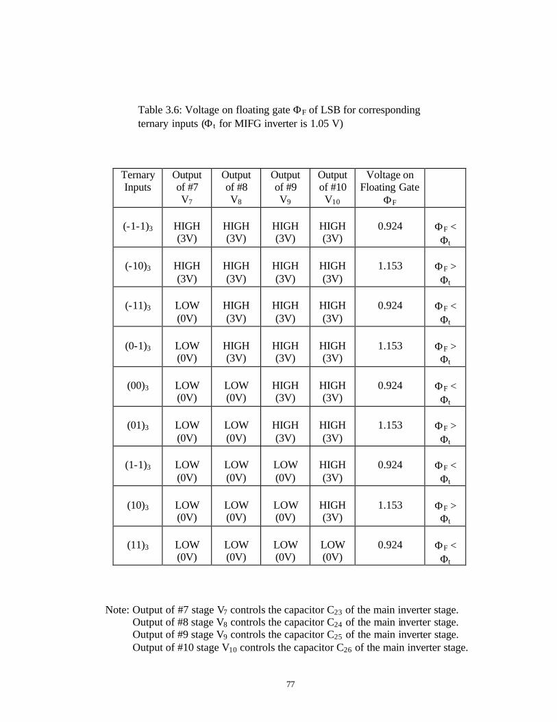
77
Table 3.6: Voltage on floating gate ΦF of LSB for corresponding ternary inputs (Φt for MIFG inverter is 1.05 V)
Ternary Inputs
Output of #7 V7
Output of #8 V8
Output of #9 V9
Output of #10 V10
Voltage on Floating Gate
ΦF
(-1-1)3
HIGH (3V)
HIGH (3V)
HIGH (3V)
HIGH (3V)
0.924
ΦF < Φt
(-10)3
HIGH (3V)
HIGH (3V)
HIGH (3V)
HIGH (3V)
1.153
ΦF > Φt
(-11)3
LOW (0V)
HIGH (3V)
HIGH (3V)
HIGH (3V)
0.924
ΦF < Φt
(0-1)3
LOW (0V)
HIGH (3V)
HIGH (3V)
HIGH (3V)
1.153
ΦF > Φt
(00)3
LOW (0V)
LOW (0V)
HIGH (3V)
HIGH (3V)
0.924
ΦF < Φt
(01)3
LOW (0V)
LOW (0V)
HIGH (3V)
HIGH (3V)
1.153
ΦF > Φt
(1-1)3
LOW (0V)
LOW (0V)
LOW (0V)
HIGH (3V)
0.924
ΦF < Φt
(10)3
LOW (0V)
LOW (0V)
LOW (0V)
HIGH (3V)
1.153
ΦF > Φt
(11)3
LOW (0V)
LOW (0V)
LOW (0V)
LOW (0V)
0.924
ΦF < Φt
Note: Output of #7 stage V7 controls the capacitor C23 of the main inverter stage. Output of #8 stage V8 controls the capacitor C24 of the main inverter stage. Output of #9 stage V9 controls the capacitor C25 of the main inverter stage. Output of #10 stage V10 controls the capacitor C26 of the main inverter stage.
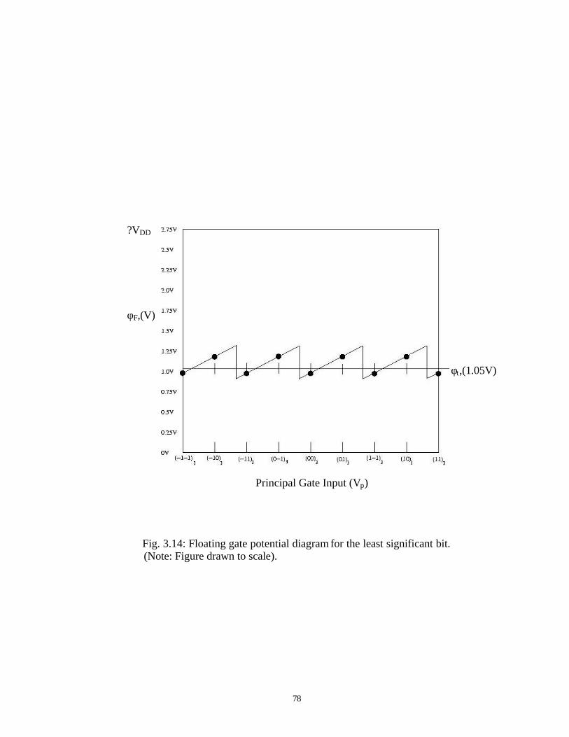
78
Fig. 3.14: Floating gate potential diagram for the least significant bit. (Note: Figure drawn to scale).
φF,(V)
φt,(1.05V)
?VDD
Principal Gate Input (Vp)
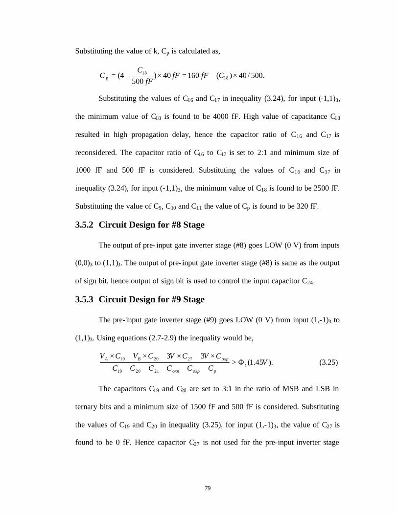
79
Substituting the value of k, Cp is calculated as,
.500/40)(16040)500
4( 1818 ×+=×+= CfFfFfF
CC p
Substituting the values of C16 and C17 in inequality (3.24), for input (-1,1)3,
the minimum value of C18 is found to be 4000 fF. High value of capacitance C18
resulted in high propagation delay, hence the capacitor ratio of C16 and C17 is
reconsidered. The capacitor ratio of C16 to C17 is set to 2:1 and minimum size of
1000 fF and 500 fF is considered. Substituting the values of C16 and C17 in
inequality (3.24), for input (-1,1)3, the minimum value of C18 is found to be 2500 fF.
Substituting the value of C9, C10 and C11 the value of Cp is found to be 320 fF.
3.5.2 Circuit Design for #8 Stage
The output of pre- input gate inverter stage (#8) goes LOW (0 V) from inputs
(0,0)3 to (1,1)3. The output of pre- input gate inverter stage (#8) is same as the output
of sign bit, hence output of sign bit is used to control the input capacitor C24.
3.5.3 Circuit Design for #9 Stage
The pre- input gate inverter stage (#9) goes LOW (0 V) from input (1,-1)3 to
(1,1)3. Using equations (2.7-2.9) the inequality would be,
).45.1(33
212019
272019 VCCCCCC
CVCVCVCVt
poxpoxn
oxpBA Φ>+++++
×+×+×+× (3.25)
The capacitors C19 and C20 are set to 3:1 in the ratio of MSB and LSB in
ternary bits and a minimum size of 1500 fF and 500 fF is considered. Substituting
the values of C19 and C20 in inequality (3.25), for input (1,-1)3, the value of C27 is
found to be 0 fF. Hence capacitor C27 is not used for the pre-input inverter stage
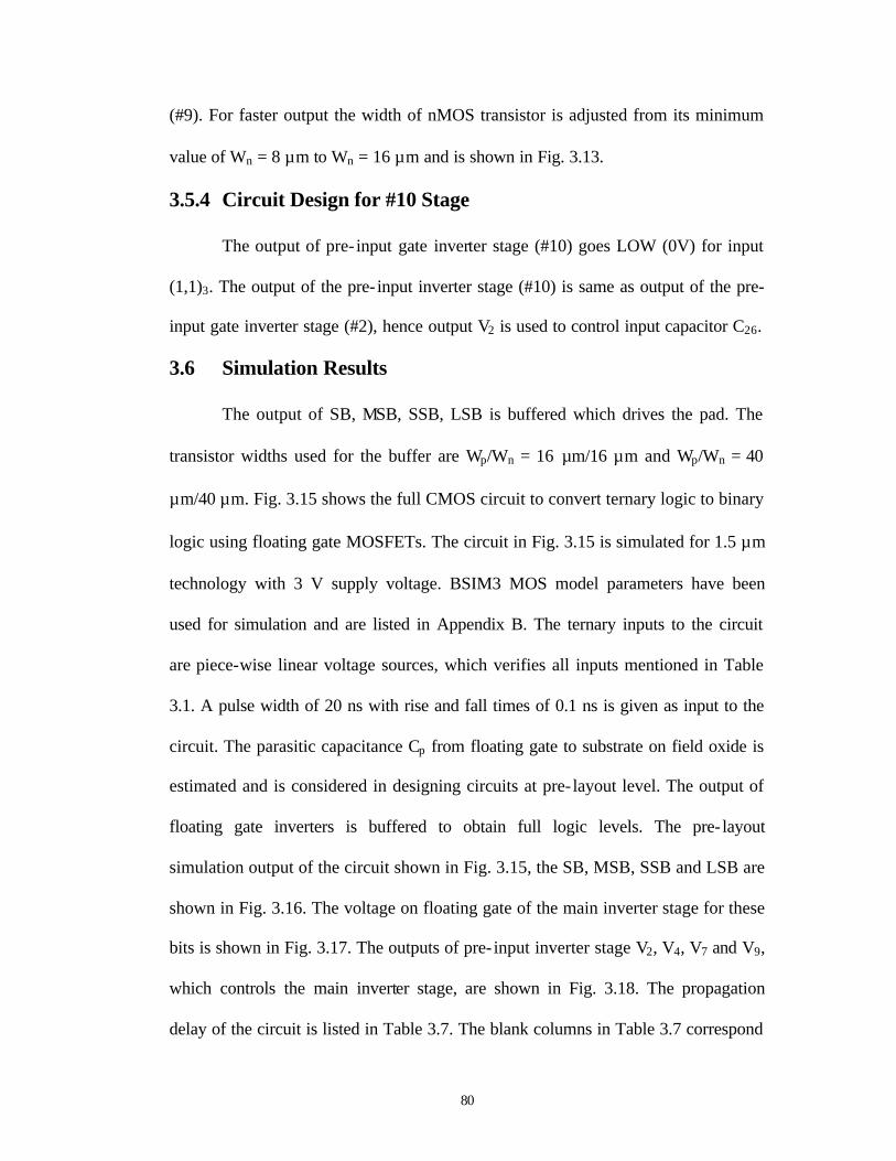
80
(#9). For faster output the width of nMOS transistor is adjusted from its minimum
value of Wn = 8 µm to Wn = 16 µm and is shown in Fig. 3.13.
3.5.4 Circuit Design for #10 Stage
The output of pre- input gate inverter stage (#10) goes LOW (0V) for input
(1,1)3. The output of the pre- input inverter stage (#10) is same as output of the pre-
input gate inverter stage (#2), hence output V2 is used to control input capacitor C26.
3.6 Simulation Results
The output of SB, MSB, SSB, LSB is buffered which drives the pad. The
transistor widths used for the buffer are Wp/Wn = 16 µm/16 µm and Wp/Wn = 40
µm/40 µm. Fig. 3.15 shows the full CMOS circuit to convert ternary logic to binary
logic using floating gate MOSFETs. The circuit in Fig. 3.15 is simulated for 1.5 µm
technology with 3 V supply voltage. BSIM3 MOS model parameters have been
used for simulation and are listed in Appendix B. The ternary inputs to the circuit
are piece-wise linear voltage sources, which verifies all inputs mentioned in Table
3.1. A pulse width of 20 ns with rise and fall times of 0.1 ns is given as input to the
circuit. The parasitic capacitance Cp from floating gate to substrate on field oxide is
estimated and is considered in designing circuits at pre- layout level. The output of
floating gate inverters is buffered to obtain full logic levels. The pre- layout
simulation output of the circuit shown in Fig. 3.15, the SB, MSB, SSB and LSB are
shown in Fig. 3.16. The voltage on floating gate of the main inverter stage for these
bits is shown in Fig. 3.17. The outputs of pre- input inverter stage V2, V4, V7 and V9,
which controls the main inverter stage, are shown in Fig. 3.18. The propagation
delay of the circuit is listed in Table 3.7. The blank columns in Table 3.7 correspond
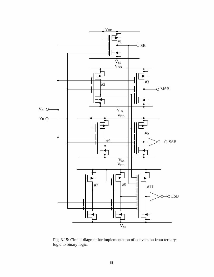
81
Fig. 3.15: Circuit diagram for implementation of conversion from ternary logic to binary logic.
VDD
VDD
VDD
VSS
VSS
VSS
SSB
LSB
#4
#6
#11#9 #7
#3 #2 MSB
VDD
VSS
SB #1
VA VB
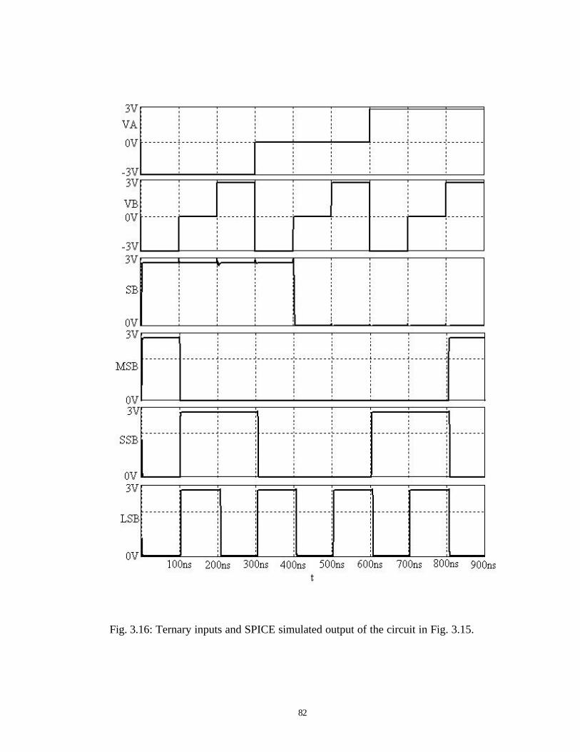
82
Fig. 3.16: Ternary inputs and SPICE simulated output of the circuit in Fig. 3.15.
83
Fig. 3.17: Ternary input and SPICE simulated voltage on floating gate of main inverter gate stages shown in Fig. 3.15.
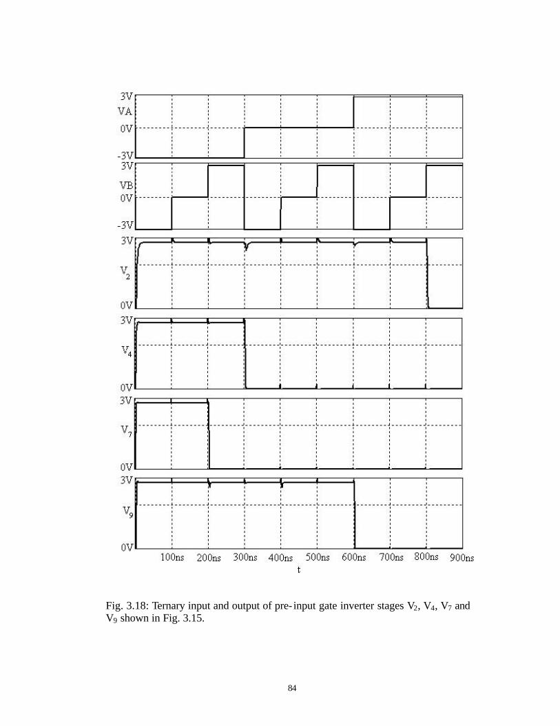
84
Fig. 3.18: Ternary input and output of pre- input gate inverter stages V2, V4, V7 and V9 shown in Fig. 3.15.
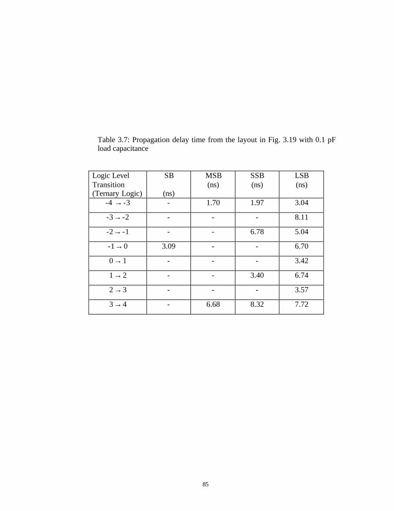
85
Table 3.7: Propagation delay time from the layout in Fig. 3.19 with 0.1 pF load capacitance
Logic Level Transition (Ternary Logic)
SB
(ns)
MSB (ns)
SSB (ns)
LSB (ns)
-4 → -3 - 1.70 1.97 3.04
-3→ -2 - - - 8.11
-2→ -1 - - 6.78 5.04
-1→0 3.09 - - 6.70
0→1 - - - 3.42
1→2 - - 3.40 6.74
2→3 - - - 3.57
3→4 - 6.68 8.32 7.72
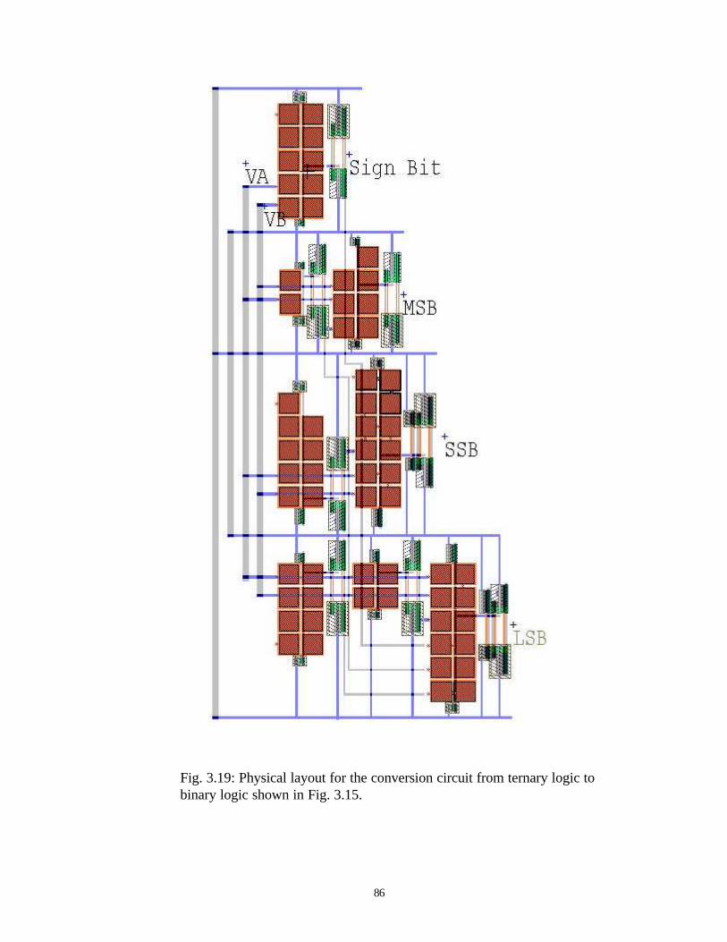
86
Fig. 3.19: Physical layout for the conversion circuit from ternary logic to binary logic shown in Fig. 3.15.
87
to no output change condition. The physical layout of the circuit in Fig. 3.15 is
drawn using Tanner Tools and is shown in Fig. 3.19. The layout occupies an area of
432 µm x 908 µm.
The layout for the circuit with padframe is shown in Fig. 3.20. The post-
layout simulation outputs of circuit with 0.1 pF load are shown in Figs. 3.21. At
testing level, capacitance offered by probes of oscilloscope and breadboard are
added to the pad pin, which is estimated to be 15 pF. Hence the circuit is also
simulated with 15 pF load and is shown in Fig. 3.22. The expected propagation
delay is presented in Table 3.8.
The worst-case variation in unit capacitance of 500 fF would be 365 fF from
Table. 2.1. The circuit is simulated using 365 fF as unit capacitance and outputs are
shown in Fig. 3.23.
3.7 Experimental Results
The conversion circuit is fabricated at MOSIS for 1.5 µm technology. The
MOS model parameters of the fabricated chip are listed in Appendix D. The
microphotograph of the fabricated design is shown in Fig. 3.24. The ternary inputs
VA and VB are connected to pin11 and pin12, respectively. The input/output pads
has protection devices from electro static discharge ESD, which are back-to-back
diodes connected to VDD and VSS. Whenever the input voltage is above VDD (3 V) or
below VSS (0 V), the respective diode is forward biased and input signal is pulled
towards VDD or VSS. In the present case, whenever logic -1 (-3 V) is given as input
to the circuit, diode connected to VSS is forward biased and is pulled towards
ground. Hence testing was limited and few transitions, which did not use logic -1 (-3
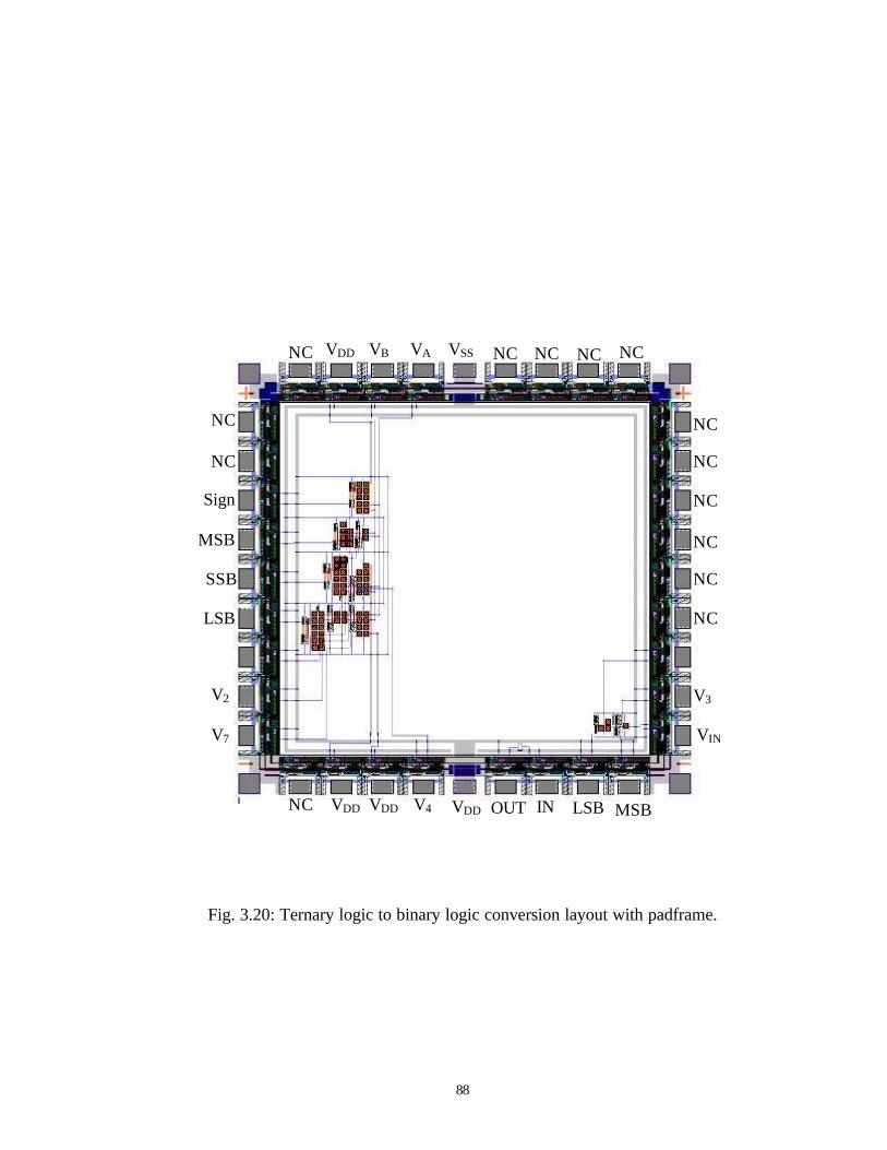
88
Fig. 3.20: Ternary logic to binary logic conversion layout with padframe.
VDD
VSS VAVB VDD
Sign
MSB
SSB
LSB
V2
V7
VDD VDD V4 OUT IN LSB MSB
VIN
V3
NC
NC
NC
NC
NC
NC
NC
NC
NC
NC
NCNCNCNC
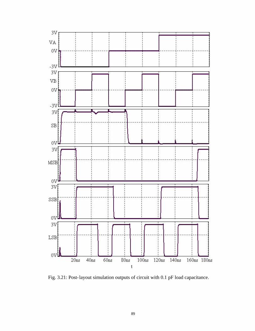
89
Fig. 3.21: Post- layout simulation outputs of circuit with 0.1 pF load capacitance.
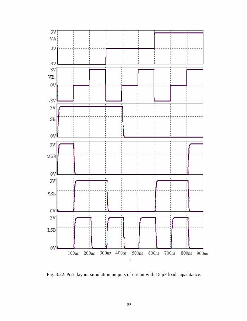
90
Fig. 3.22: Post- layout simulation outputs of circuit with 15 pF load capacitance.
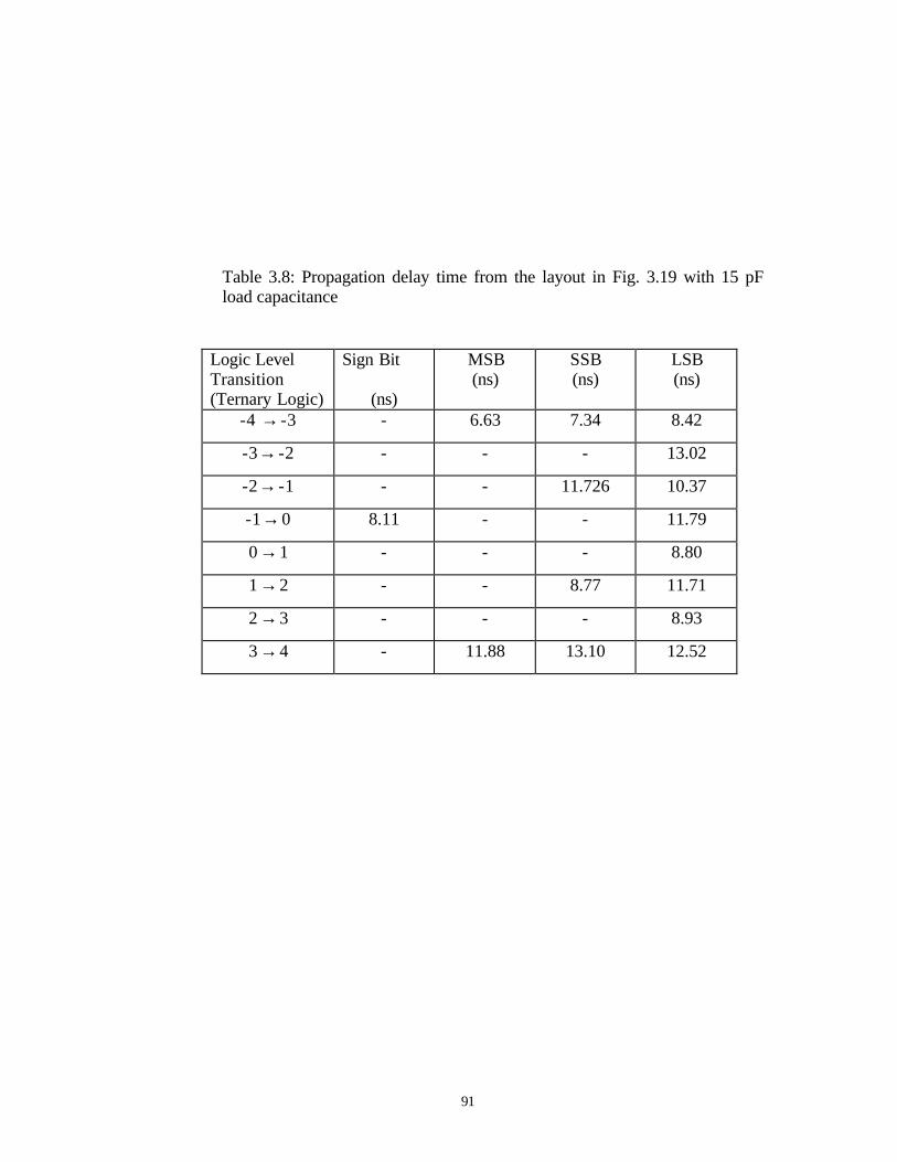
91
Table 3.8: Propagation delay time from the layout in Fig. 3.19 with 15 pF load capacitance
Logic Level Transition (Ternary Logic)
Sign Bit
(ns)
MSB (ns)
SSB (ns)
LSB (ns)
-4 → -3 - 6.63 7.34 8.42
-3→ -2 - - - 13.02
-2→ -1 - - 11.726 10.37
-1→0 8.11 - - 11.79
0→1 - - - 8.80
1→2 - - 8.77 11.71
2→3 - - - 8.93
3→4 - 11.88 13.10 12.52
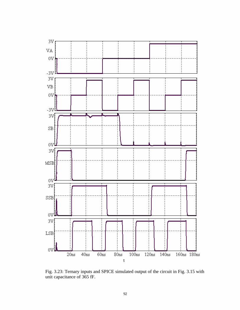
92
Fig. 3.23: Ternary inputs and SPICE simulated output of the circuit in Fig. 3.15 with unit capacitance of 365 fF.
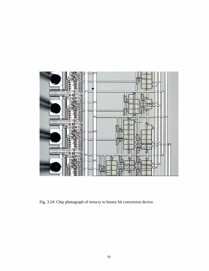
93
Fig. 3.24: Chip photograph of terna ry to binary bit conversion device.
94
V) could be tested on the fabricated device. The padframe design is being
investigated and revised for balanced ternary logic implementation and is left as
scope for future work.
The capacitors C3, C11 and C18 are used to adjust the threshold voltage for
sign bit, V4 and V7, respectively. The capacitors C3, C11 and C18 are connected to
VDD in the design. The inputs to these capacitors can be controlled at pin13, pin27
and pin28. The voltage at these pins is controlled using external voltage sources to
adjust threshold voltage of the MIFG inverters.
95
Chapter 4
Conversion from Quaternary Logic to Binary Logic
4.1 Overview
The quaternary logic system is expressed in the form of (0,1,2,3). In a
standard 3 V CMOS process, logic levels 0, 1, 2 and 3 are defined as 0 V, 1 V, 2 V
and 3 V, respectively. Table 4.1 shows quaternary logic levels and corresponding
binary bits. Corresponding decimal number is also included in Table 4.1. The
conversion circuits from quaternary logic to binary logic presented here uses MIFG
MOSFETs. The principle of transistor switching ON or OFF depending on the
calculated weighted sum of all inputs on floating gate greater than or less than
switching threshold voltage is utilized in designing the conversion circuits.
4.2 Circuit Design for MSB
The circuits are designed for 1.5 µm technology with a 3 V supply voltage.
The switching threshold voltage of a CMOS inverter is found from voltage transfer
characteristics. The standard CMOS inverter shown in Fig. 4.1 is simulated with
W/L=16.0 µm/1.6 µm for a 3 V supply voltage. The W/L ratio of the transistors is
taken more than the minimum values to obtain faster timing response. DC analysis
is performed to obtain voltage transfer characteristics (VTC). The VTC is shown in
Fig. 4.2, and Φg0 and Φs1 are marked. Φg0 and Φs1 are input voltages at which the
output of inverter is VDD-0.1 V and 0.1 V, respectively. Φg0 is 0.53 V and Φs1 is
2.37 V. The switching threshold voltage Φt is obtained using equation (2.7),
.45.12
37.253.0Vt =
+=Φ (4.1)
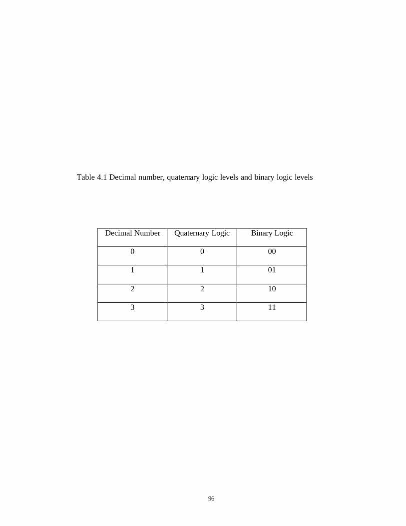
96
Table 4.1 Decimal number, quaternary logic levels and binary logic levels
Decimal Number Quaternary Logic Binary Logic
0 0 00
1 1 01
2 2 10
3 3 11
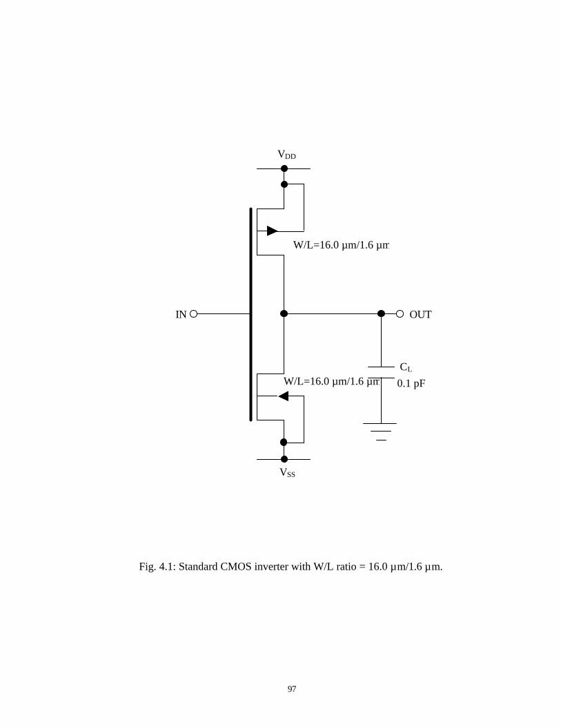
97
Fig. 4.1: Standard CMOS inverter with W/L ratio = 16.0 µm/1.6 µm.
IN OUT
CL
0.1 pF
VDD
VSS
W/L=16.0 µm/1.6 µm
W/L=16.0 µm/1.6 µm
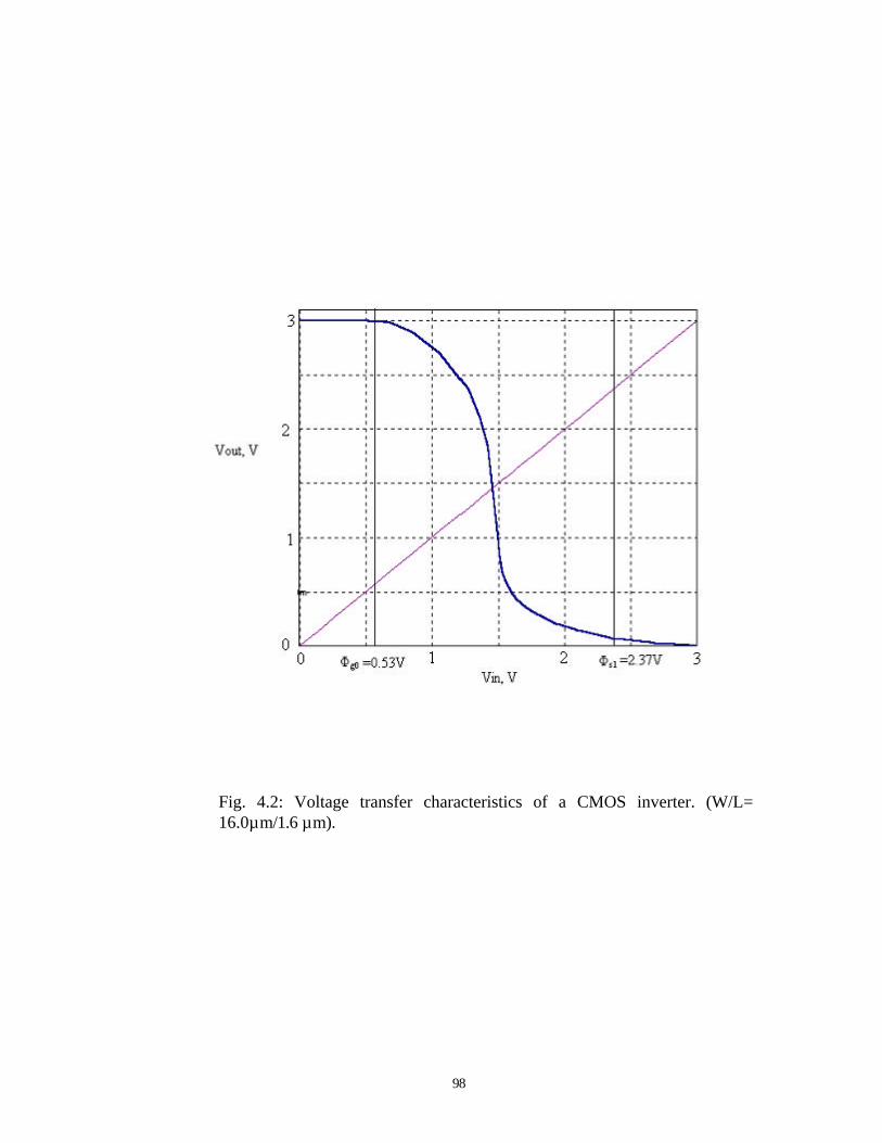
98
Fig. 4.2: Voltage transfer characteristics of a CMOS inverter. (W/L= 16.0µm/1.6 µm).
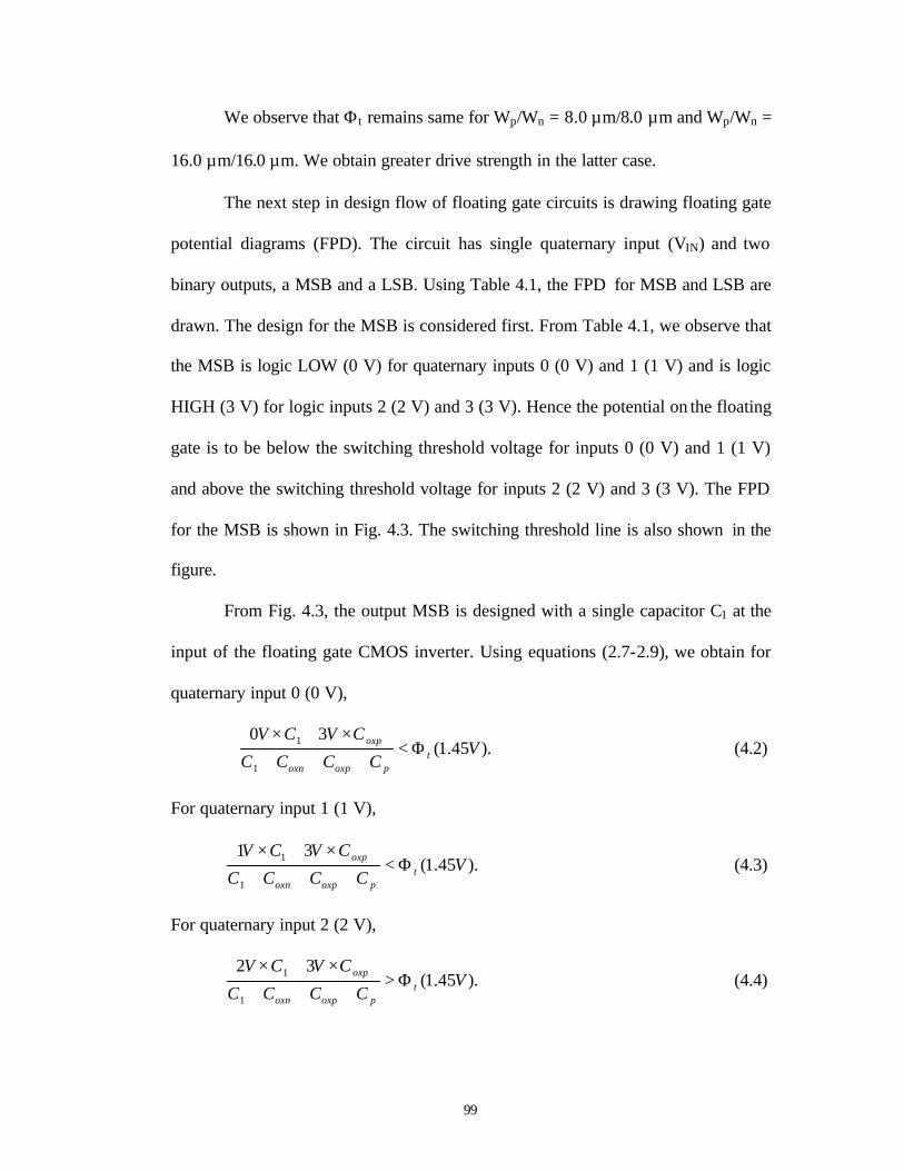
99
We observe that Φt remains same for Wp/Wn = 8.0 µm/8.0 µm and Wp/Wn =
16.0 µm/16.0 µm. We obtain greater drive strength in the latter case.
The next step in design flow of floating gate circuits is drawing floating gate
potential diagrams (FPD). The circuit has single quaternary input (VIN) and two
binary outputs, a MSB and a LSB. Using Table 4.1, the FPD for MSB and LSB are
drawn. The design for the MSB is considered first. From Table 4.1, we observe that
the MSB is logic LOW (0 V) for quaternary inputs 0 (0 V) and 1 (1 V) and is logic
HIGH (3 V) for logic inputs 2 (2 V) and 3 (3 V). Hence the potential on the floating
gate is to be below the switching threshold voltage for inputs 0 (0 V) and 1 (1 V)
and above the switching threshold voltage for inputs 2 (2 V) and 3 (3 V). The FPD
for the MSB is shown in Fig. 4.3. The switching threshold line is also shown in the
figure.
From Fig. 4.3, the output MSB is designed with a single capacitor C1 at the
input of the floating gate CMOS inverter. Using equations (2.7-2.9), we obtain for
quaternary input 0 (0 V),
).45.1(30
1
1 VCCCC
CVCVt
poxpoxn
oxp Φ<+++
×+× (4.2)
For quaternary input 1 (1 V),
).45.1(31
1
1 VCCCC
CVCVt
poxpoxn
oxp Φ<+++
×+× (4.3)
For quaternary input 2 (2 V),
).45.1(32
1
1 VCCCC
CVCVt
poxpoxn
oxp Φ>+++
×+× (4.4)
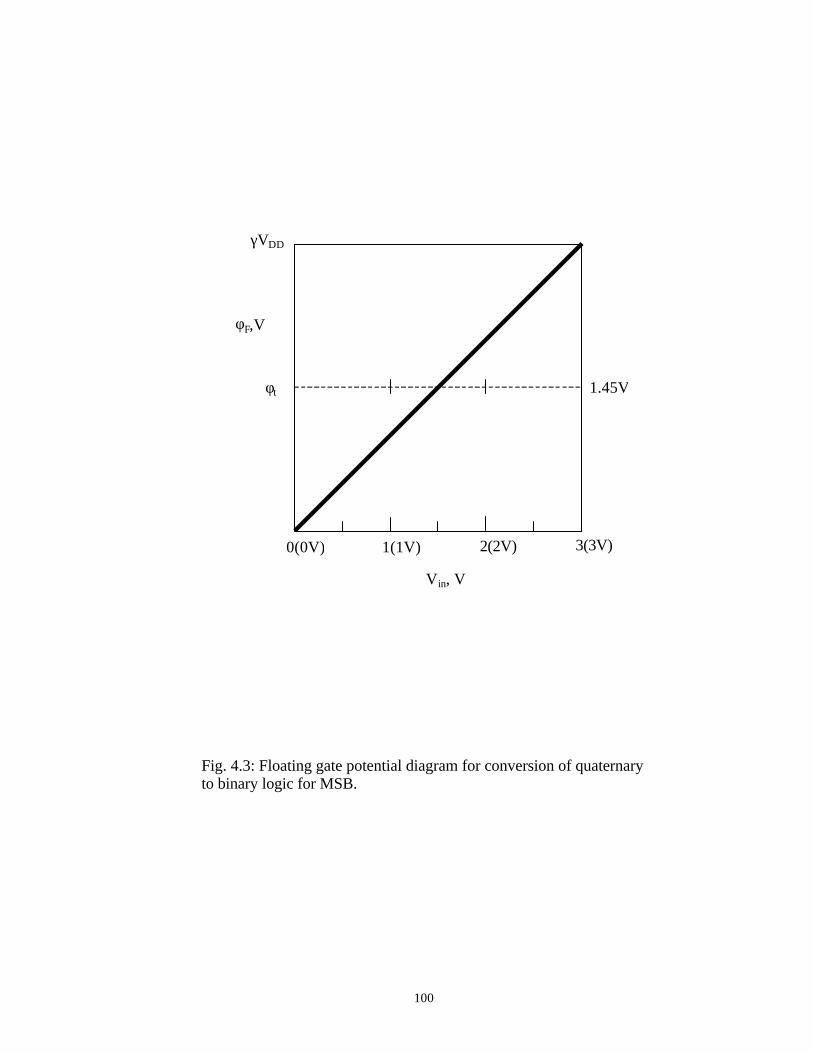
100
Fig. 4.3: Floating gate potential diagram for conversion of quaternary to binary logic for MSB.
γVDD
φF,V
Vin, V
0(0V) 1(1V) 2(2V) 3(3V)
φt 1.45V
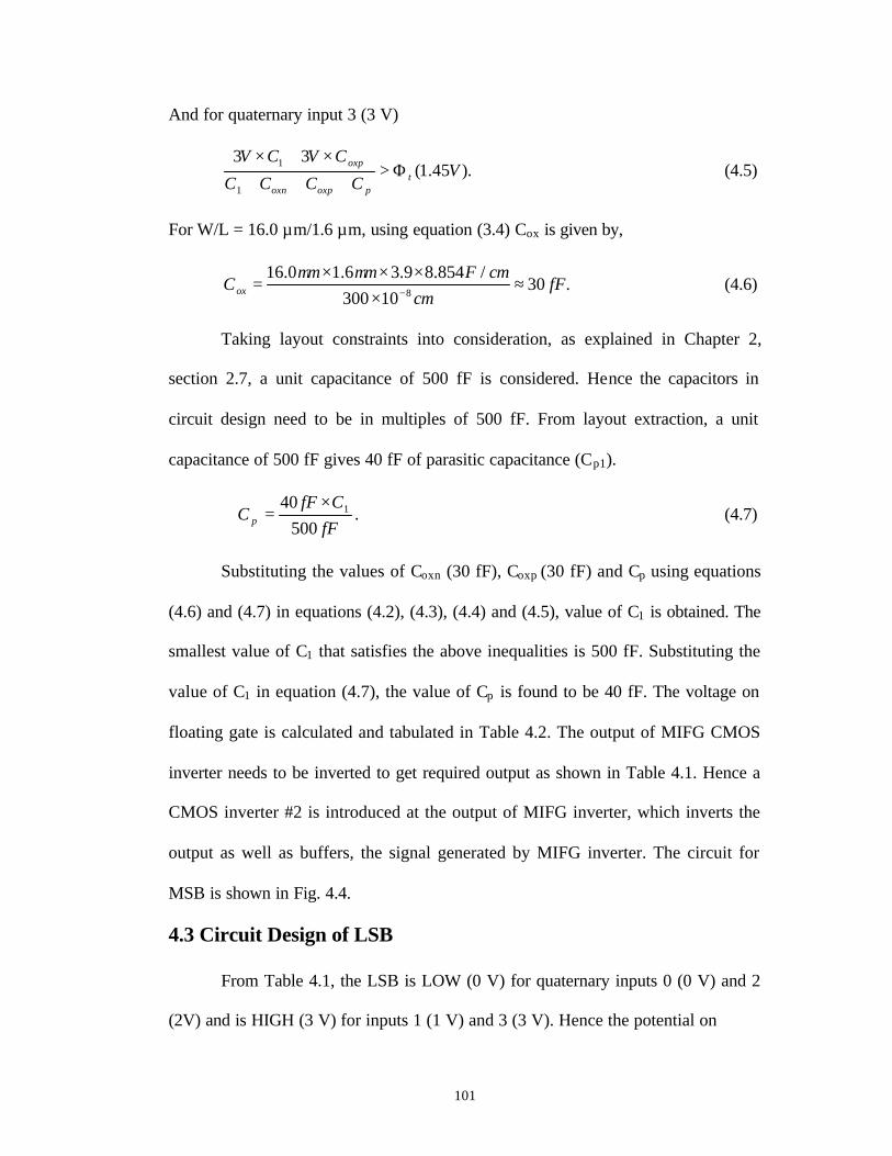
101
And for quaternary input 3 (3 V)
).45.1(33
1
1 VCCCC
CVCVt
poxpoxn
oxp Φ>+++
×+× (4.5)
For W/L = 16.0 µm/1.6 µm, using equation (3.4) Cox is given by,
.3010300
/854.89.36.10.168
fFcm
cmFmmCox ≈
××××
=−
µµ (4.6)
Taking layout constraints into consideration, as explained in Chapter 2,
section 2.7, a unit capacitance of 500 fF is considered. Hence the capacitors in
circuit design need to be in multiples of 500 fF. From layout extraction, a unit
capacitance of 500 fF gives 40 fF of parasitic capacitance (Cp1).
.500
40 1
fFCfF
C p
×=∴ (4.7)
Substituting the values of Coxn (30 fF), Coxp (30 fF) and Cp using equations
(4.6) and (4.7) in equations (4.2), (4.3), (4.4) and (4.5), value of C1 is obtained. The
smallest value of C1 that satisfies the above inequalities is 500 fF. Substituting the
value of C1 in equation (4.7), the value of Cp is found to be 40 fF. The voltage on
floating gate is calculated and tabulated in Table 4.2. The output of MIFG CMOS
inverter needs to be inverted to get required output as shown in Table 4.1. Hence a
CMOS inverter #2 is introduced at the output of MIFG inverter, which inverts the
output as well as buffers, the signal generated by MIFG inverter. The circuit for
MSB is shown in Fig. 4.4.
4.3 Circuit Design of LSB
From Table 4.1, the LSB is LOW (0 V) for quaternary inputs 0 (0 V) and 2
(2V) and is HIGH (3 V) for inputs 1 (1 V) and 3 (3 V). Hence the potential on
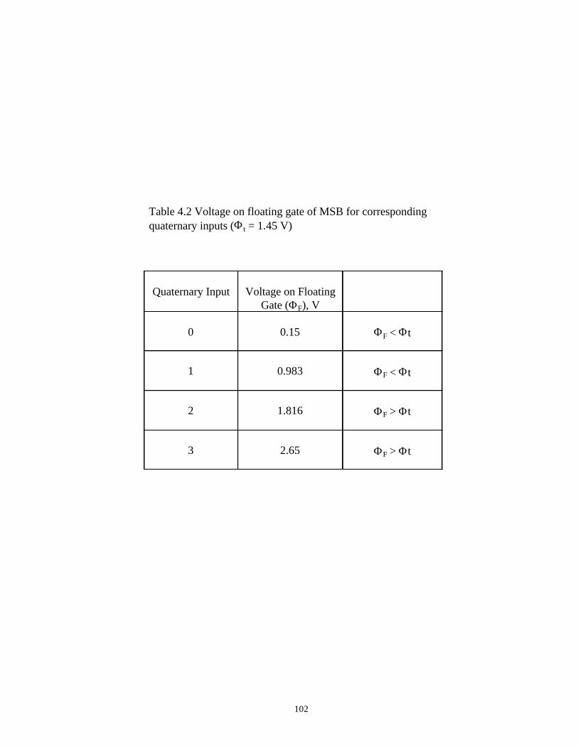
102
Table 4.2 Voltage on floating gate of MSB for corresponding quaternary inputs (Φt = 1.45 V)
Quaternary Input
Voltage on Floating
Gate (ΦF), V
0
0.15
ΦF < Φt
1
0.983
ΦF < Φt
2
1.816
ΦF > Φt
3
2.65
ΦF > Φt
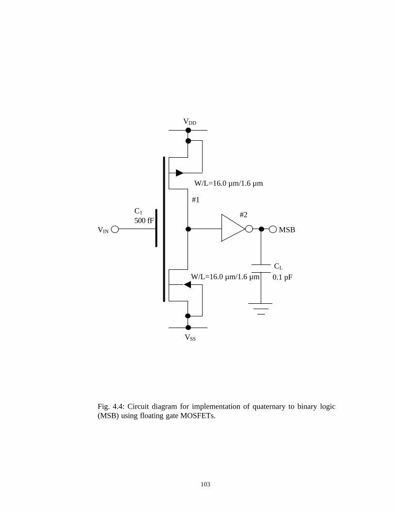
103
Fig. 4.4: Circuit diagram for implementation of quaternary to binary logic (MSB) using floating gate MOSFETs.
VIN MSB
CL 0.1 pF
VDD
VSS
W/L=16.0 µm/1.6 µm
W/L=16.0 µm/1.6 µm
C1 500 fF
#1
#2
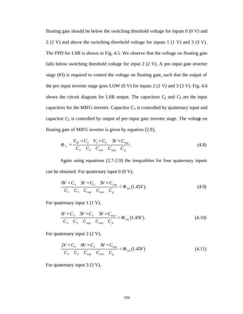
104
floating gate should be below the switching threshold voltage for inputs 0 (0 V) and
2 (2 V) and above the switching threshold voltage for inputs 1 (1 V) and 3 (3 V).
The FPD for LSB is shown in Fig. 4.5. We observe that the voltage on floating gate
falls below switching threshold voltage for input 2 (2 V). A pre- input gate inverter
stage (#3) is required to control the voltage on floating gate, such that the output of
the pre- input inverter stage goes LOW (0 V) for inputs 2 (2 V) and 3 (3 V). Fig. 4.6
shows the circuit diagram for LSB output. The capacitors C2 and C3 are the input
capacitors for the MIFG inverter. Capacitor C3 is controlled by quaternary input and
capacitor C2 is controlled by output of pre- input gate inverter stage. The voltage on
floating gate of MIFG inverter is given by equation (2.9),
.3
32
233
poxpoxn
oxpINF CCCCC
CVCVCV
++++
×+×+×=Φ (4.8)
Again using equations (2.7-2.9) the inequalities for four quaternary inputs
can be obtained. For quaternary input 0 (0 V),
).45.1(330
32
23 VCCCCC
CVCVCVinv
poxnoxp
oxp Φ<++++
×+×+× (4.9)
For quaternary input 1 (1 V),
).45.1(331
32
23 VCCCCC
CVCVCVinv
poxnoxp
oxp Φ>++++
×+×+× (4.10)
For quaternary input 2 (2 V),
)45.1(302
32
23 VCCCCC
CVCVCVinv
poxnoxp
oxp Φ<++++
×+×+× (4.11)
For quaternary input 3 (3 V),
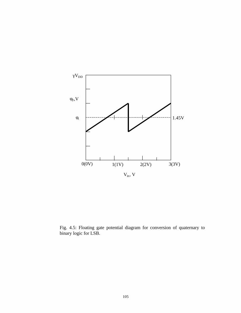
105
Fig. 4.5: Floating gate potential diagram for conversion of quaternary to binary logic for LSB.
γVDD
Vin, V
0(0V) 1(1V) 2(2V) 3(3V)
φF,V
φt 1.45V
106
Fig. 4.6: Circuit diagram for implementation of quaternary logic to binary logic (LSB) using floating gate MOSFETs.
VIN LSB
CL
0.1 pF
VDD
VSS
W/L= 16.0 µm/ 1.6 µm
W/L= 16.0 µm/1.6 µm
C4 500 fF
#3 #5
W/L= 16.0 µm/1.6 µm
W/L= 16.0 µm/1.6 µm
#4
C3 1000 fF
C2 500 fF
107
).45.1(303
32
23 VCCCCC
CVCVCVinv
poxnoxp
oxp Φ>++++
×+×+× (4.12)
Again 500 fF of unit capacitance gives 40 fF of parasitic capacitance (Cp1).
The value of Cp is given by,
.500
)(40 32
fFCCfF
C p
+×=∴ (4.13)
Substitute the value of Coxn (30 fF), Coxp (30 fF) and Cp using equations (4.6)
and (4.13) in equations (4.9), (4.10), (4.11) and (4.12) to obtain the values of C2 and
C3. For the above inequalities to satisfy, the value of capacitor C3 should be more
than the value of capacitor C2. Plug in the values for C2 and C3, which are multiples
of 500 fF. Capacitors C2 and C3 are found to be 500 fF and 1000 fF, which satisfy
the above inequalities. Substituting the va lue of C2 and C3 in equation (4.13), the
value of Cp is found to be 120 fF. The voltage on floating gate is calculated and
tabulated in Table 4.3. The output of MIFG CMOS inverter (#4) needs to be
inverted to get the required output as shown in the Table 4.1. Hence a CMOS
inverter #5 is introduced at the output of MIFG CMOS inverter.
4.3.1 Circuit Design for #3 Stage
The pre-input inverter stage (#3) in Fig. 4.6 controlling the capacitor C2 is to
be designed such that the output of the inverter stage is HIGH (3 V) for inputs 0 (0
V) and 1 (1 V) and is LOW (0 V) for inputs 2 (2 V) and 3 (3 V). Using equations
(2.7-2.9) the inequalities for (#3) inverter stage are obtained. For quaternary input 0
).45.1(30
4
4 VCCCC
CVCVinv
poxpoxn
oxp Φ<+++
×+× (4.14)
For quaternary input 1 (1 V),
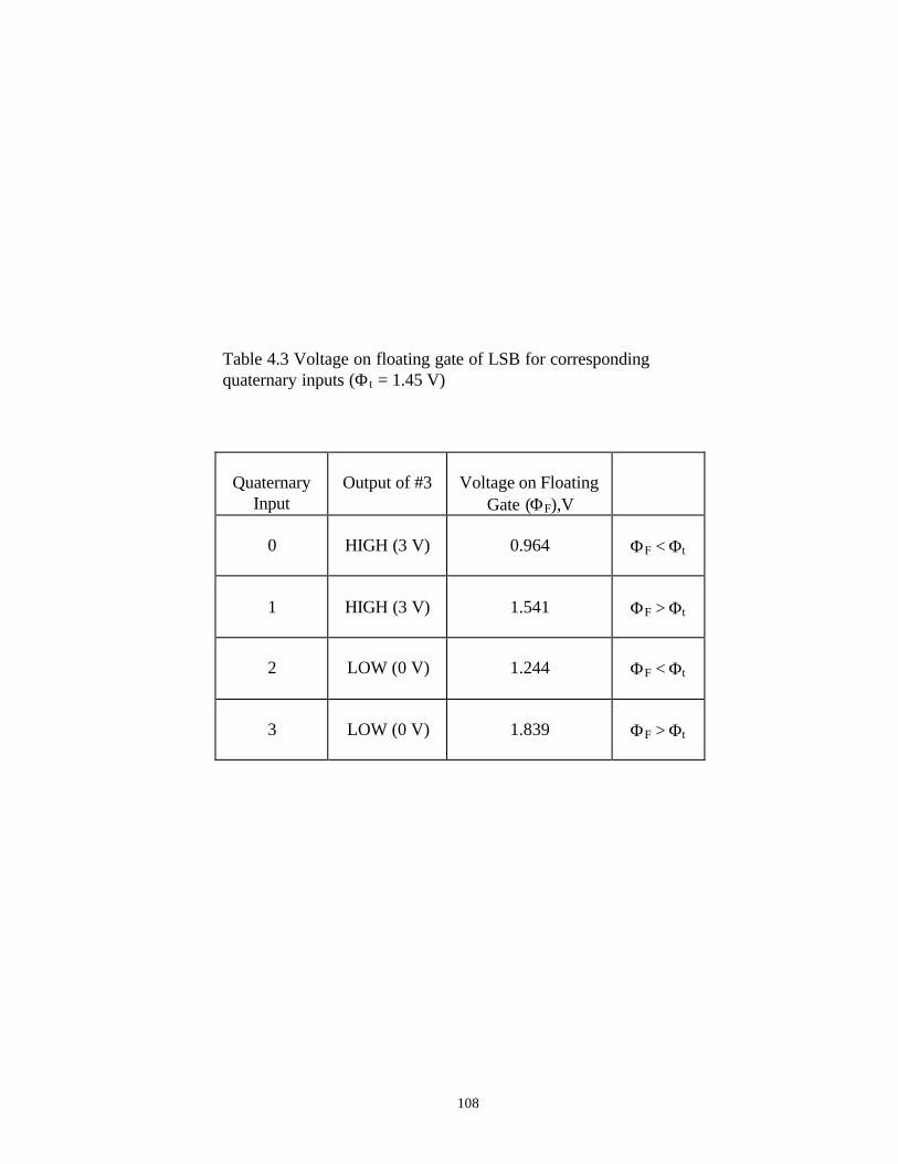
108
Table 4.3 Voltage on floating gate of LSB for corresponding quaternary inputs (Φt = 1.45 V)
Quaternary
Input
Output of #3
Voltage on Floating
Gate (ΦF),V
0
HIGH (3 V)
0.964
ΦF < Φt
1
HIGH (3 V)
1.541
ΦF > Φt
2
LOW (0 V)
1.244
ΦF < Φt
3
LOW (0 V)
1.839
ΦF > Φt
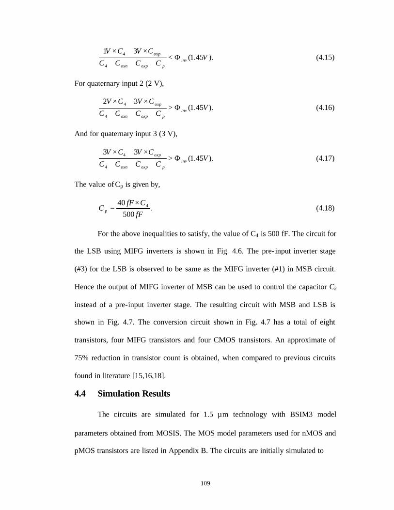
109
).45.1(31
4
4 VCCCC
CVCVinv
poxpoxn
oxp Φ<+++
×+× (4.15)
For quaternary input 2 (2 V),
).45.1(32
4
4 VCCCC
CVCVinv
poxpoxn
oxp Φ>+++
×+× (4.16)
And for quaternary input 3 (3 V),
).45.1(33
4
4 VCCCC
CVCVinv
poxpoxn
oxp Φ>+++
×+× (4.17)
The value of Cp is given by,
.500
40 4
fFCfF
C p
×= (4.18)
For the above inequalities to satisfy, the value of C4 is 500 fF. The circuit for
the LSB using MIFG inverters is shown in Fig. 4.6. The pre- input inverter stage
(#3) for the LSB is observed to be same as the MIFG inverter (#1) in MSB circuit.
Hence the output of MIFG inverter of MSB can be used to control the capacitor C2
instead of a pre-input inverter stage. The resulting circuit with MSB and LSB is
shown in Fig. 4.7. The conversion circuit shown in Fig. 4.7 has a total of eight
transistors, four MIFG transistors and four CMOS transistors. An approximate of
75% reduction in transistor count is obtained, when compared to previous circuits
found in literature [15,16,18].
4.4 Simulation Results
The circuits are simulated for 1.5 µm technology with BSIM3 model
parameters obtained from MOSIS. The MOS model parameters used for nMOS and
pMOS transistors are listed in Appendix B. The circuits are initially simulated to
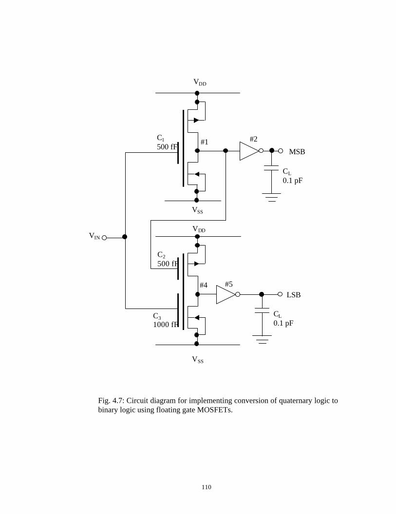
110
Fig. 4.7: Circuit diagram for implementing conversion of quaternary logic to binary logic using floating gate MOSFETs.
VIN
MSB
VDD
VSS
LSB
VDD
VSS
C1 500 fF
C2 500 fF
C3 1000 fF
#1 #2
#4 #5
CL 0.1 pF
CL 0.1 pF

111
verify proper functionality of the circuit. A ramp input from 0 V to 3 V is given as
input to the circuit. The output of MSB and LSB are shown in Figs. 4.8 and 4.9. The
voltage on floating gate of MSB and LSB are shown in Figs. 4.10 and 4.11. The
circuit is verified for all possible transitions of quaternary input [18]. A piece-wise-
linear voltage source with 0.1 ns rise and fall time with 40 ns pulse width is given at
input of the circuit. The output of MSB and LSB is shown in Fig. 4.12. The physical
design for the circuit in Fig. 4.7 is shown in Fig. 4.13. The layout occupies an area
of 130 × 175 µm2. The post- layout simulation includes the extracted parasitic
capacitances and a load capacitance of 0.1 pF is added at the output. The post- layout
simulation output is shown in Fig. 4.14. The propagation delay is measured from 50
percent point of input to 50 percent point of output. For example, when input
transits from logic 2 (2 V) to 3 (3 V), the delay is considered from 50 percent
between 2 (2 V) and 3 (3 V) i.e. 2.5V (2 V + 0.5×(3 V-2 V) = 2.5 V) to 50 percent
of output i.e. at 1.5 V. Table 4.4 provides the propagation delays. The worst-case
delay of tpLH ˜ 6 ns for input transitions 2(2 V) → 1(1 V) and tpHL ˜ 5 ns for input
transition of 1(1 V) → 2(2 V) are noted. Few columns in Table 4.4 are not filled;
this is accounts for no change in the output of circuit for the given change in input.
The present work is compared with previous works [15,16,18], to date and is
summarized in Table 4.5. The worst-case value of unit capacitance due to
discrepancies in the fabrication is 365 fF. The circuit was simulated with unit
capacitance of 365 fF and the outputs are shown in Fig. 4.15. The capacitance
formed between floating gate and substrate on field oxide was estimated and taken
into account in pre-layout simulations.
112
Fig. 4.8: Quaternary input and SPICE simulated output (MSB) for the circuit in Fig. 4.4.
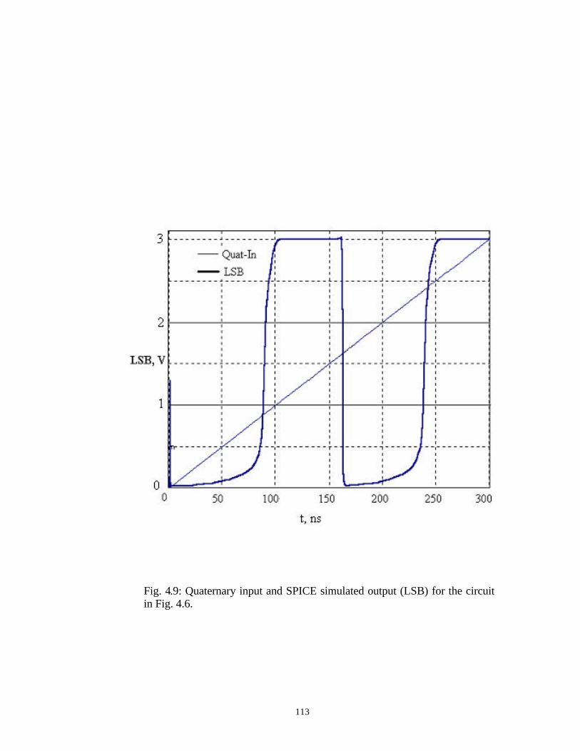
113
Fig. 4.9: Quaternary input and SPICE simulated output (LSB) for the circuit in Fig. 4.6.
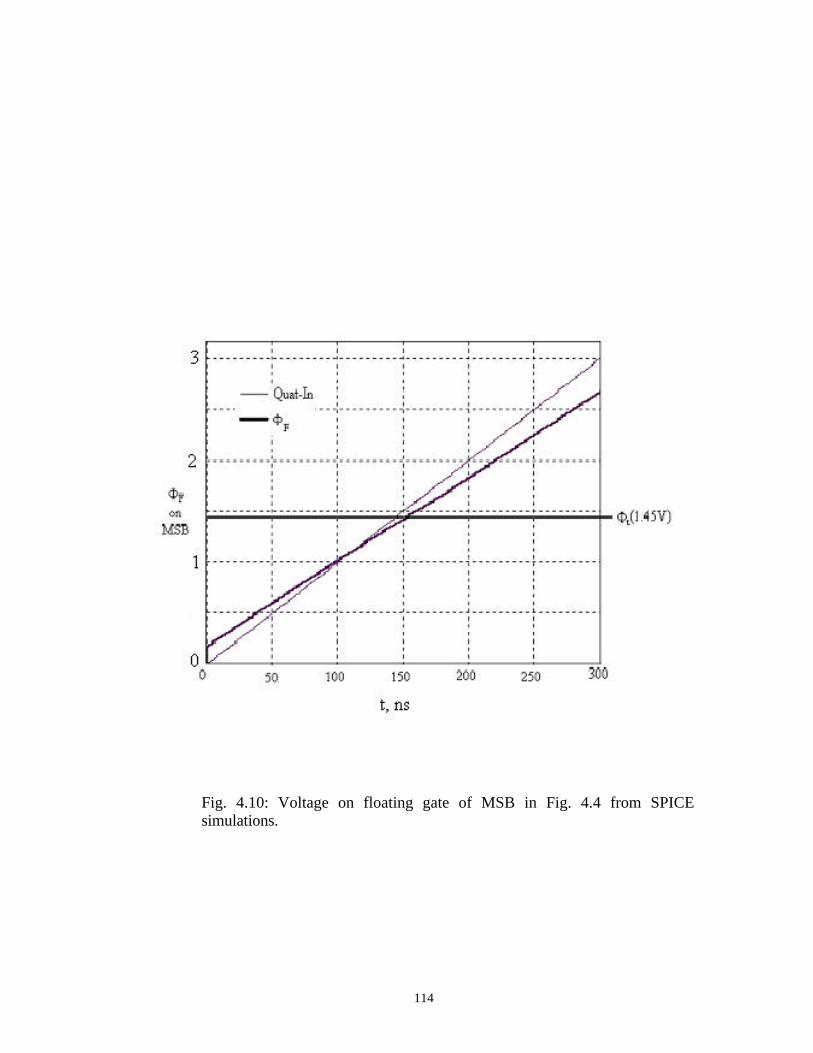
114
Fig. 4.10: Voltage on floating gate of MSB in Fig. 4.4 from SPICE simulations.
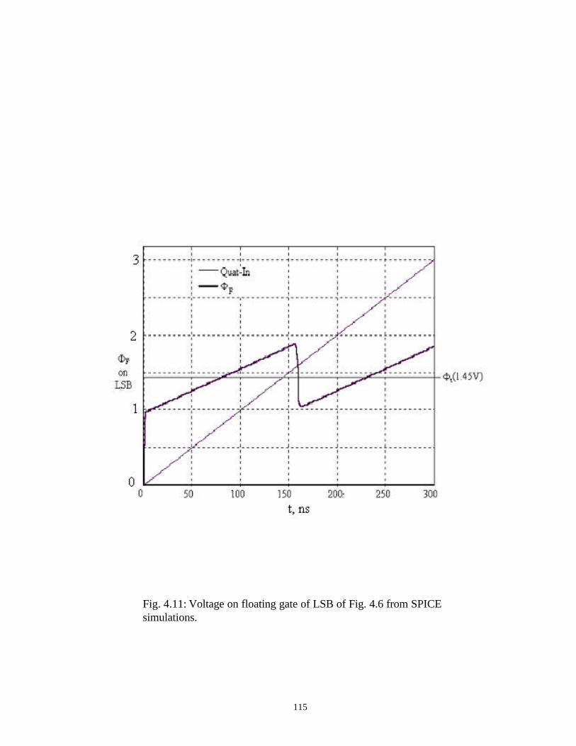
115
Fig. 4.11: Voltage on floating gate of LSB of Fig. 4.6 from SPICE simulations.
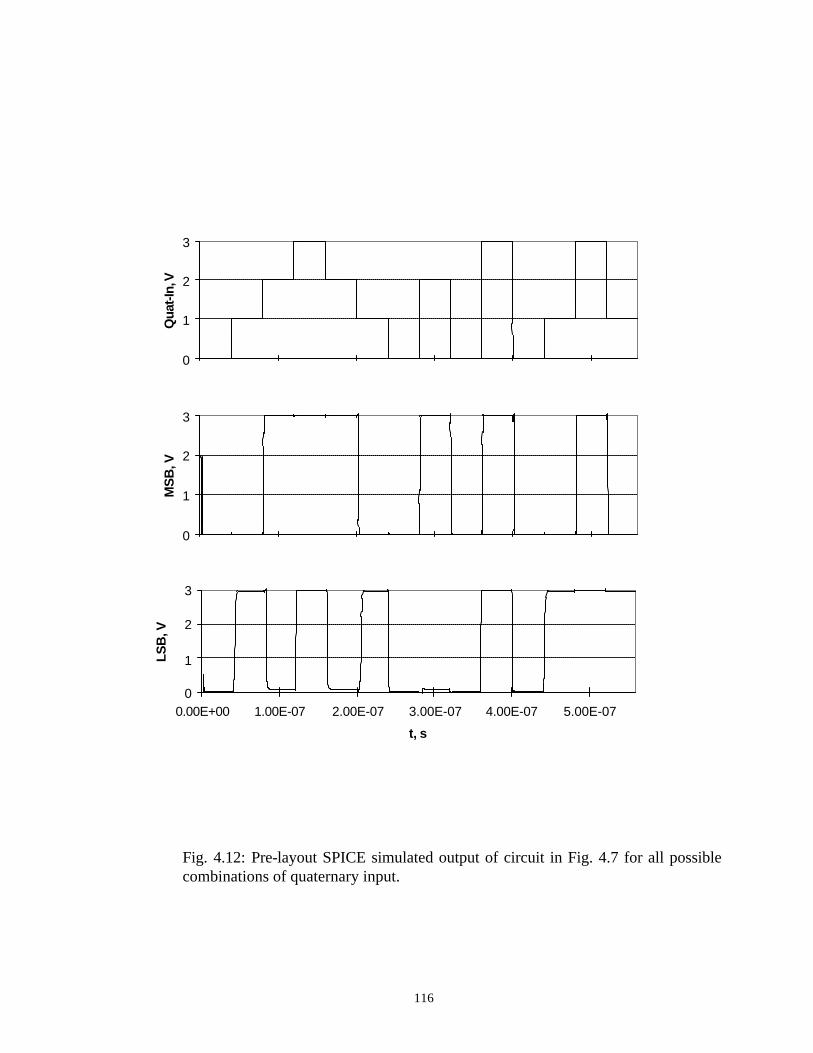
116
Fig. 4.12: Pre-layout SPICE simulated output of circuit in Fig. 4.7 for all possible combinations of quaternary input.
0
1
2
3
Qua
t-In,
V
0
1
2
3
MS
B, V
0
1
2
3
0.00E+00 1.00E-07 2.00E-07 3.00E-07 4.00E-07 5.00E-07
t, s
LSB
, V
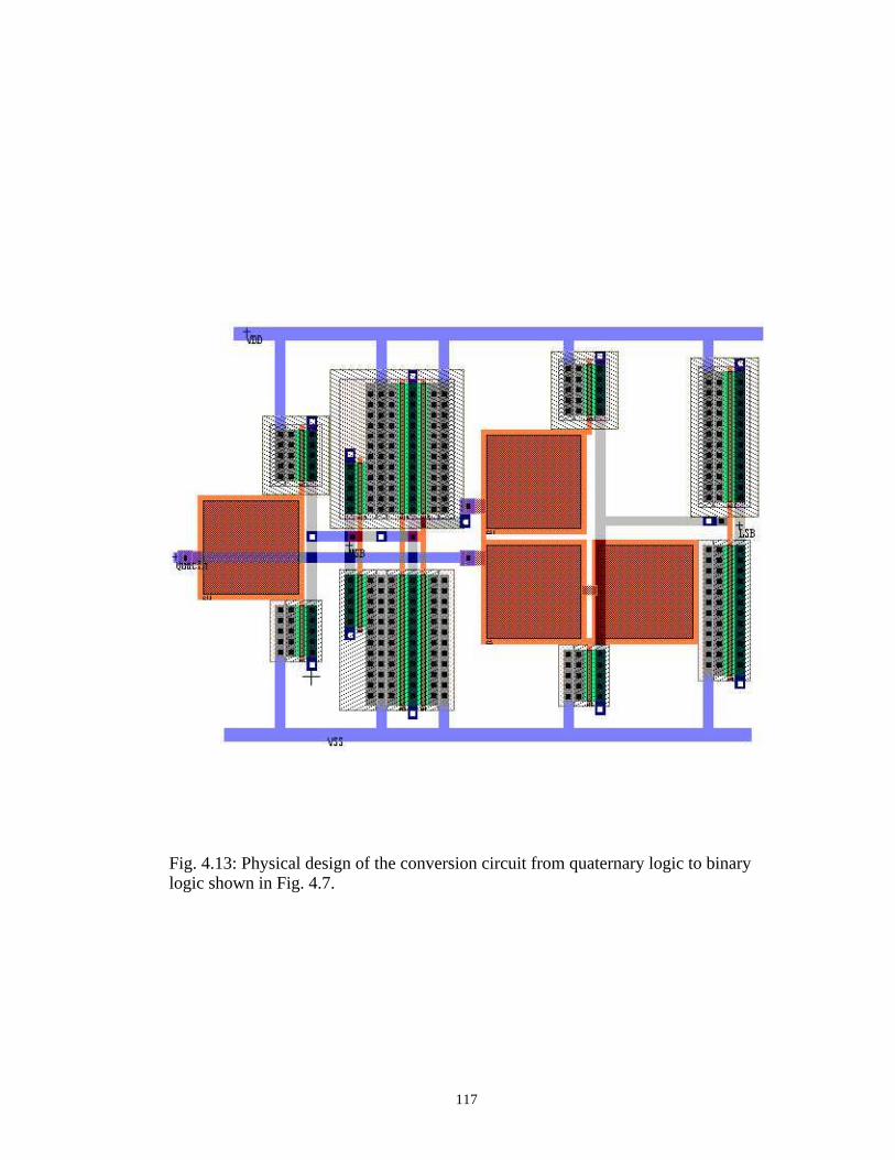
117
Fig. 4.13: Physical design of the conversion circuit from quaternary logic to binary logic shown in Fig. 4.7.
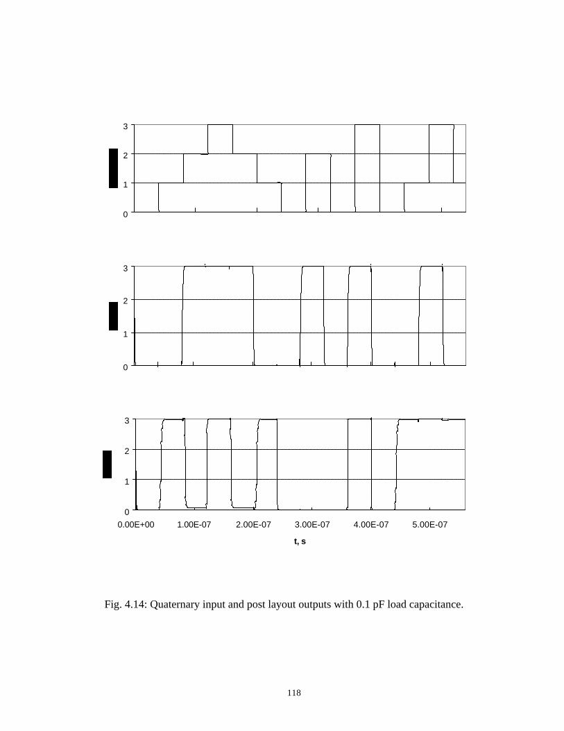
118
Fig. 4.14: Quaternary input and post layout outputs with 0.1 pF load capacitance.
0
1
2
3
0
1
2
3
0
1
2
3
0.00E+00 1.00E-07 2.00E-07 3.00E-07 4.00E-07 5.00E-07
t, s
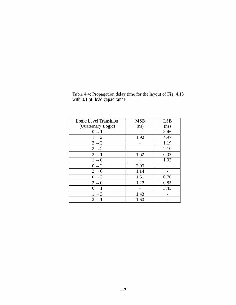
119
Table 4.4: Propagation delay time for the layout of Fig. 4.13 with 0.1 pF load capacitance
Logic Level Transition (Quaternary Logic)
MSB (ns)
LSB (ns)
0→1 - 3.46 1→2 1.92 4.97 2→3 - 1.19 3→2 - 2.10 2→1 1.52 6.02 1→0 - 1.02 0→2 2.03 - 2→0 1.14 - 0→3 1.51 0.70 3→0 1.22 0.85 0→1 - 3.45 1→3 1.43 - 3→1 1.63 -
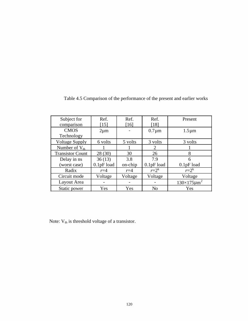
120
Table 4.5 Comparison of the performance of the present and earlier works
Subject for comparison
Ref. [15]
Ref. [16]
Ref. [18]
Present
CMOS Technology
2µm - 0.7µm 1.5µm
Voltage Supply 6 volts 5 volts 3 volts 3 volts Number of Vth 1 1 2 1
Transistor Count 28 (30) 30 26 8 Delay in ns (worst case)
36 (13) 0.1pF load
3.8 on-chip
7.9 0.1pF load
6 0.1pF load
Radix r=4 r=4 r=2k r=2k Circuit mode Voltage Voltage Voltage Voltage Layout Area - - - 130×175µm2 Static power Yes Yes No Yes
Note: Vth is threshold voltage of a transistor.
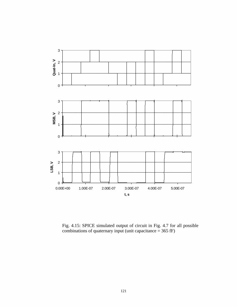
121
Fig. 4.15: SPICE simulated output of circuit in Fig. 4.7 for all possible combinations of quaternary input (unit capacitance = 365 fF)
0
1
2
3Q
uat-
In, V
0
1
2
3
MS
B, V
0
1
2
3
0.00E+00 1.00E-07 2.00E-07 3.00E-07 4.00E-07 5.00E-07
t, s
LSB
, V
122
4.5 Experimental Results
The design was fabricated in AMI 1.5 µm CMOS process. Fig. 4.16 shows a
photomicrograph of the chip. The MOS model parameters of the fabricated chip are
obtained from the MOSIS (T1AZ) and are listed in Appendix D. The voltage
transfer characteristic of CMOS inverter shown in Fig. 4.1 is simulated with
fabricated MOS model parameters and is shown in Fig. 4.17. The value of Φg0
(0.66V) and Φs1 (1.64 V) are obtained from voltage transfer characteristics. The
switching threshold voltage (Φt) of CMOS inverter is obtained using equation (2.7),
.15.12
64.166.0V
VVt =
+=Φ (4.19)
The simulation value of 1.15 V agrees with experimental value of 1.1 V. While the
switching threshold voltage with MOS model parameters used for the design is
1.45V (refer equation (4.1)). The voltage on floating gate (ΦF) of MSB and LSB
obtained using equations (4.2- 4.5) and (4.9-4.12) are compared with Φt (1.15 V)
and tabulated in Tables 4.6 and 4.7, respectively. It is found that for logic 2 (2 V)
input, the inequality in equation (4.11) does not satisfy. ΦF should be less than Φt
not greater than Φt. The extracted design from the layout with parasitic capacitances
is resimulated with BSIM3 MOS model parameters of the fabricated design. The
simulation output of MSB and LSB for a ramp input of 0 V to 3 V is shown in Fig.
4.18 and Fig. 4.19. The simulation output shows incorrect output at LSB for logic 2
(2 V), which should be LOW instead of HIGH. The fabricated chip is tested for
input ranging from 0 V to 3 V and measured values are tabulated.
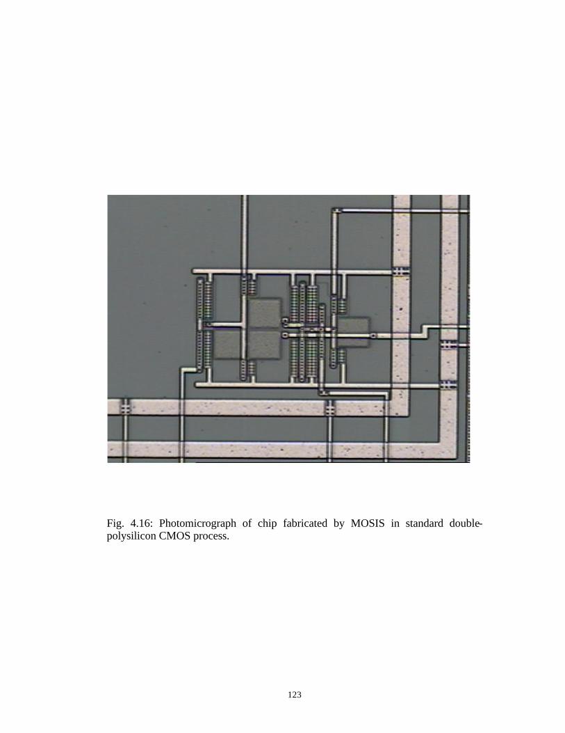
123
Fig. 4.16: Photomicrograph of chip fabricated by MOSIS in standard double-polysilicon CMOS process.
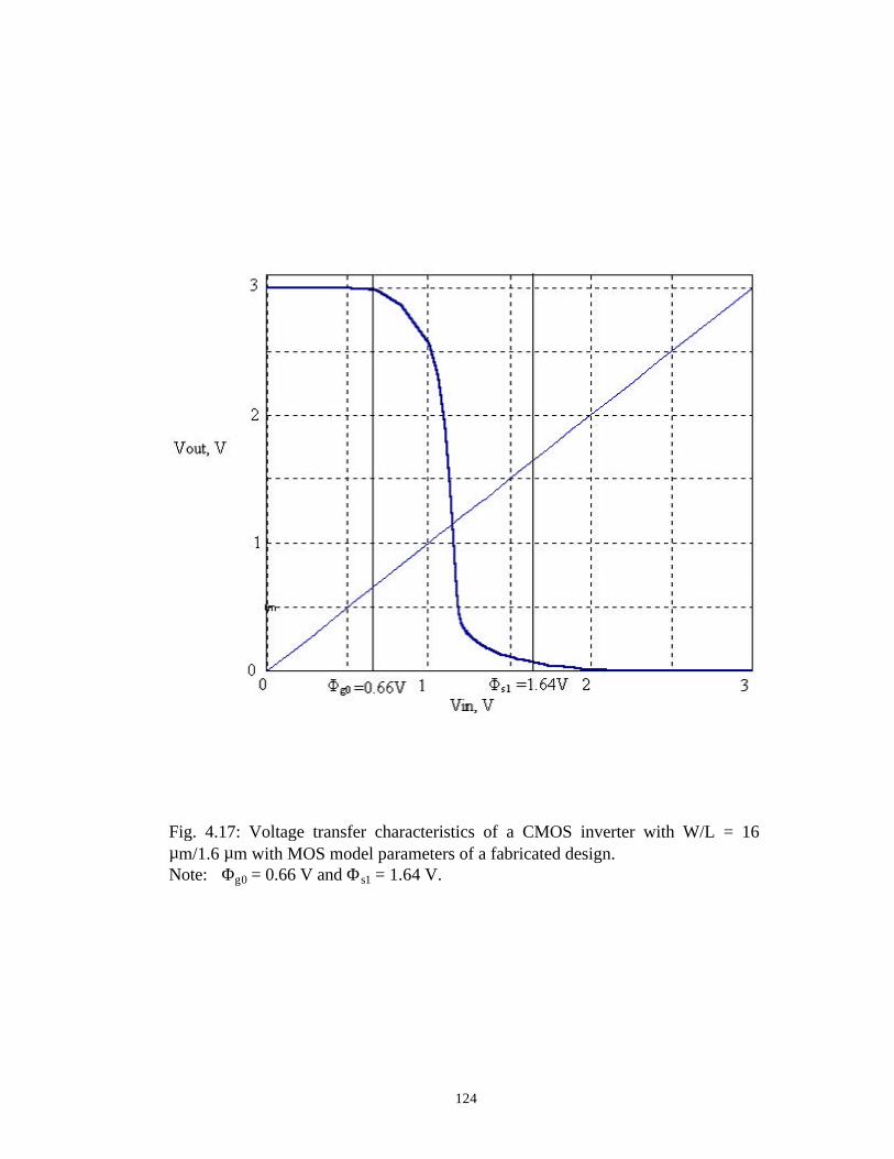
124
Fig. 4.17: Voltage transfer characteristics of a CMOS inverter with W/L = 16 µm/1.6 µm with MOS model parameters of a fabricated design. Note: Φg0 = 0.66 V and Φs1 = 1.64 V.
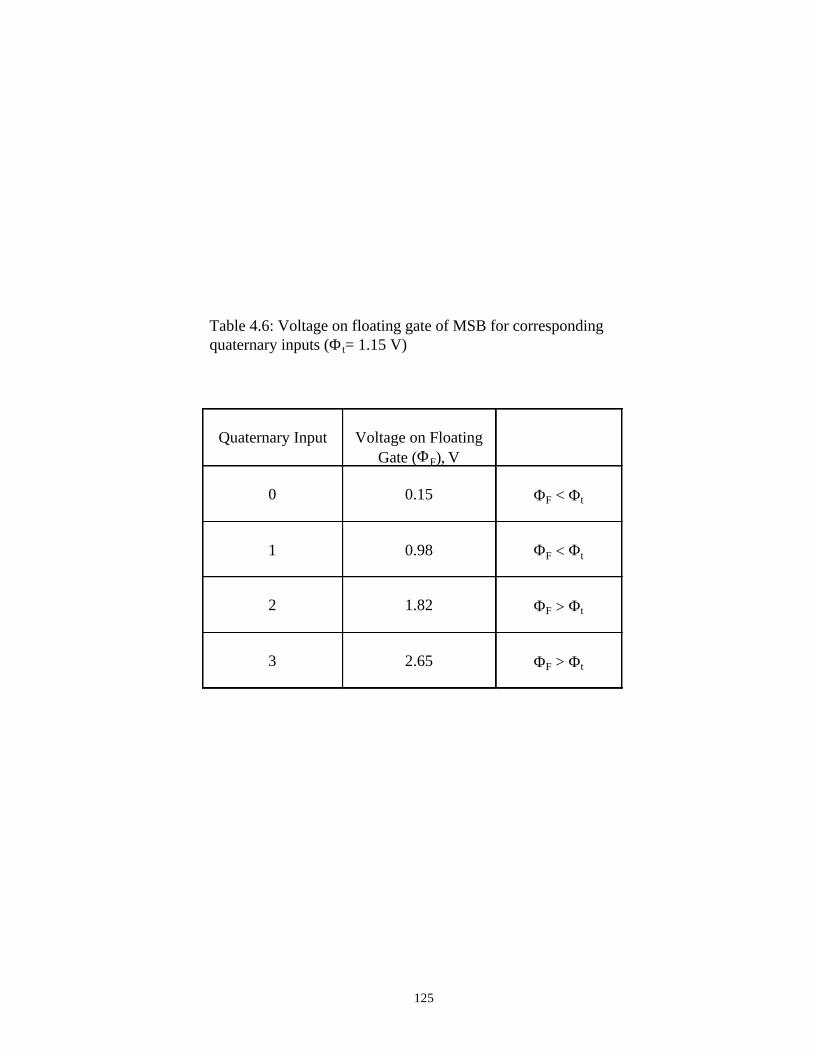
125
Table 4.6: Voltage on floating gate of MSB for corresponding quaternary inputs (Φt= 1.15 V)
Quaternary Input
Voltage on Floating
Gate (ΦF), V
0
0.15
ΦF < Φt
1
0.98
ΦF < Φt
2
1.82
ΦF > Φt
3
2.65
ΦF > Φt
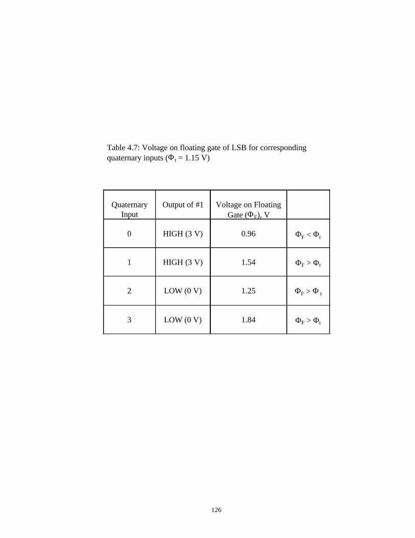
126
Table 4.7: Voltage on floating gate of LSB for corresponding quaternary inputs (Φt = 1.15 V)
Quaternary
Input
Output of #1
Voltage on Floating
Gate (ΦF), V
0
HIGH (3 V)
0.96
ΦF < Φt
1
HIGH (3 V)
1.54
ΦF > Φt
2
LOW (0 V)
1.25
ΦF > Φ t
3
LOW (0 V)
1.84
ΦF > Φt
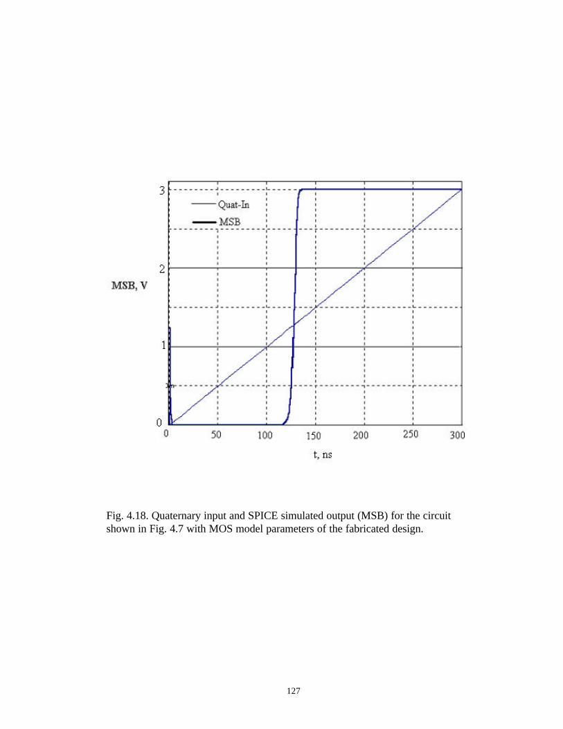
127
Fig. 4.18. Quaternary input and SPICE simulated output (MSB) for the circuit shown in Fig. 4.7 with MOS model parameters of the fabricated design.
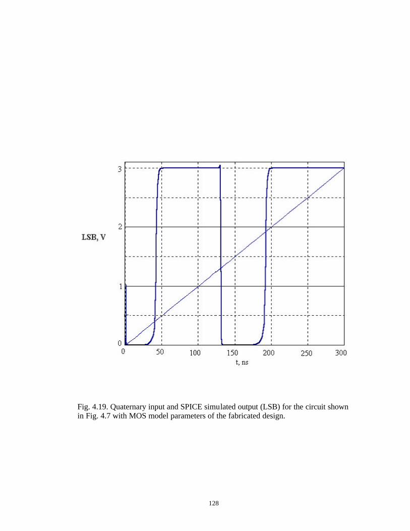
128
Fig. 4.19. Quaternary input and SPICE simulated output (LSB) for the circuit shown in Fig. 4.7 with MOS model parameters of the fabricated design.
129
Figure 4.20 shows the experimental results from oscilloscope. The measured
values are compared with simulated data with MOS model parameters used for
design, MOS model parameters of fabricated chip and are summarized in Tables 4.8
and 4.9, respectively. Figures 4.21 and 4.22 shows the corresponding plots. From
measured and simulated data we observe, the maximum voltage that has output
corresponding to logic 2 is (1.6 V). Table 4.10 summarizes the voltages of the
quaternary logic inputs that give appropriate binary output. With 1.6 V as logic 2,
the design is re-simulated with MOS model parameters of fabricated chip for all
possible transitions in input and is shown in Fig. 4.23 with 0.1 pF load capacitance.
The layout extract is also re-simulated with 1.6 V as logic 2 and is shown in Fig.
4.24. The layout extract is simulated with MOS model parameters of fabricated chip
for all possible transitions in input to compare simulated and measured propagation
delay. A piece wise linear input with 5 ns rise and fall time and 1 us pulse width is
given as input. A 15 pF load capacitance is added at the output as probe capacitance.
The output drivers driving the pads are considered for simulations to obtain accurate
results. The simulated output of MSB and LSB is shown in Fig. 4.25. The
propagation delay of the simulated results from Fig. 4.25 is compared with
measured values and is tabulated in Table 4.11.
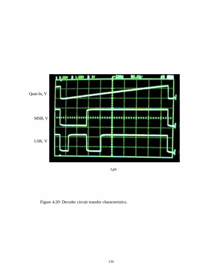
130
Figure 4.20: Decoder circuit transfer characteristics.
Quat-In, V
MSB, V
LSB, V
t,µs
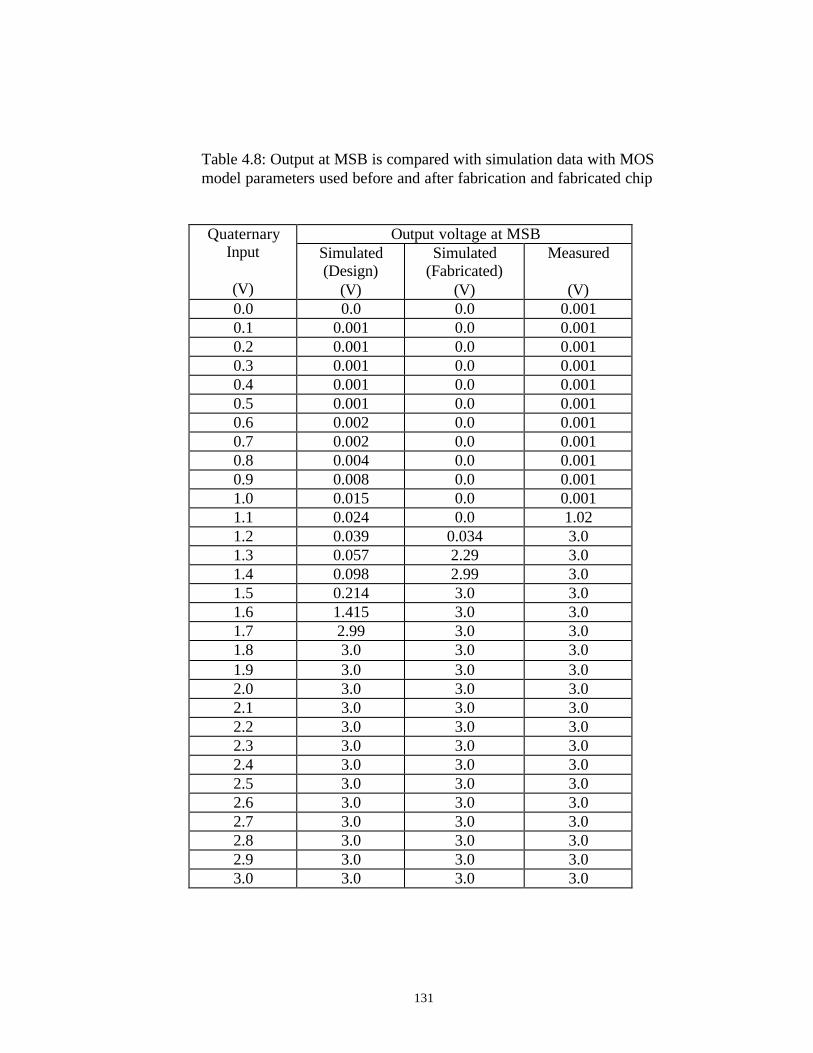
131
Table 4.8: Output at MSB is compared with simulation data with MOS model parameters used before and after fabrication and fabricated chip
Output voltage at MSB Quaternary Input
(V)
Simulated (Design)
(V)
Simulated (Fabricated)
(V)
Measured
(V) 0.0 0.0 0.0 0.001 0.1 0.001 0.0 0.001 0.2 0.001 0.0 0.001 0.3 0.001 0.0 0.001 0.4 0.001 0.0 0.001 0.5 0.001 0.0 0.001 0.6 0.002 0.0 0.001 0.7 0.002 0.0 0.001 0.8 0.004 0.0 0.001 0.9 0.008 0.0 0.001 1.0 0.015 0.0 0.001 1.1 0.024 0.0 1.02 1.2 0.039 0.034 3.0 1.3 0.057 2.29 3.0 1.4 0.098 2.99 3.0 1.5 0.214 3.0 3.0 1.6 1.415 3.0 3.0 1.7 2.99 3.0 3.0 1.8 3.0 3.0 3.0 1.9 3.0 3.0 3.0 2.0 3.0 3.0 3.0 2.1 3.0 3.0 3.0 2.2 3.0 3.0 3.0 2.3 3.0 3.0 3.0 2.4 3.0 3.0 3.0 2.5 3.0 3.0 3.0 2.6 3.0 3.0 3.0 2.7 3.0 3.0 3.0 2.8 3.0 3.0 3.0 2.9 3.0 3.0 3.0 3.0 3.0 3.0 3.0
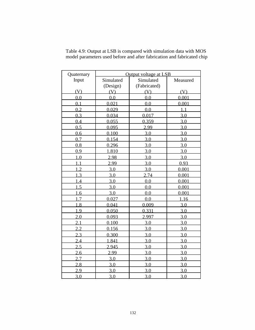
132
Table 4.9: Output at LSB is compared with simulation data with MOS model parameters used before and after fabrication and fabricated chip
Output voltage at LSB Quaternary Input
(V)
Simulated (Design)
(V)
Simulated (Fabricated)
(V)
Measured
(V) 0.0 0.0 0.0 0.001 0.1 0.021 0.0 0.001 0.2 0.029 0.0 1.1 0.3 0.034 0.017 3.0 0.4 0.055 0.359 3.0 0.5 0.095 2.99 3.0 0.6 0.100 3.0 3.0 0.7 0.154 3.0 3.0 0.8 0.296 3.0 3.0 0.9 1.810 3.0 3.0 1.0 2.98 3.0 3.0 1.1 2.99 3.0 0.93 1.2 3.0 3.0 0.001 1.3 3.0 2.74 0.001 1.4 3.0 0.0 0.001 1.5 3.0 0.0 0.001 1.6 3.0 0.0 0.001 1.7 0.027 0.0 1.16 1.8 0.041 0.009 3.0 1.9 0.050 0.331 3.0 2.0 0.093 2.997 3.0 2.1 0.100 3.0 3.0 2.2 0.156 3.0 3.0 2.3 0.300 3.0 3.0 2.4 1.841 3.0 3.0 2.5 2.945 3.0 3.0 2.6 2.99 3.0 3.0 2.7 3.0 3.0 3.0 2.8 3.0 3.0 3.0 2.9 3.0 3.0 3.0 3.0 3.0 3.0 3.0
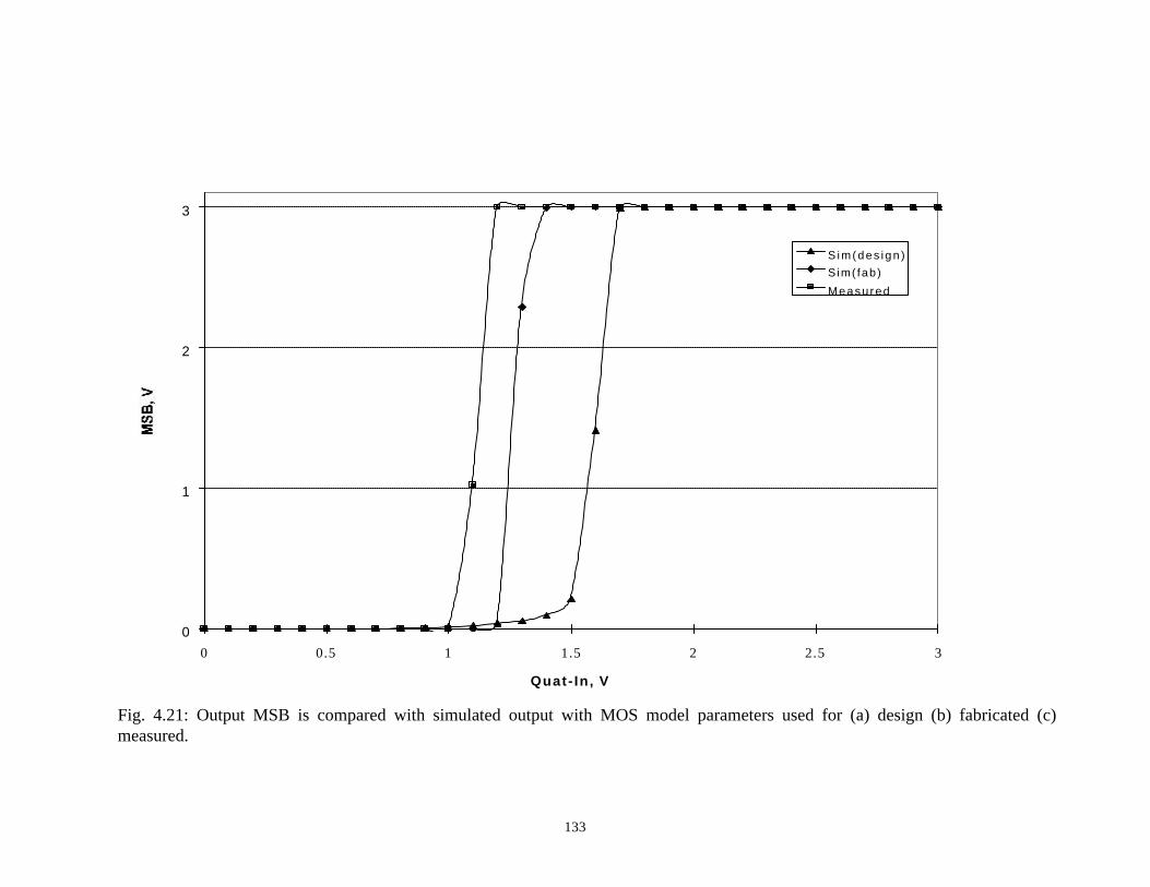
133
Fig. 4.21: Output MSB is compared with simulated output with MOS model parameters used for (a) design (b) fabricated (c) measured.
0
1
2
3
0 0.5 1 1.5 2 2.5 3
Quat- In, V
S im(des ign )
S im( fab)
Measu red
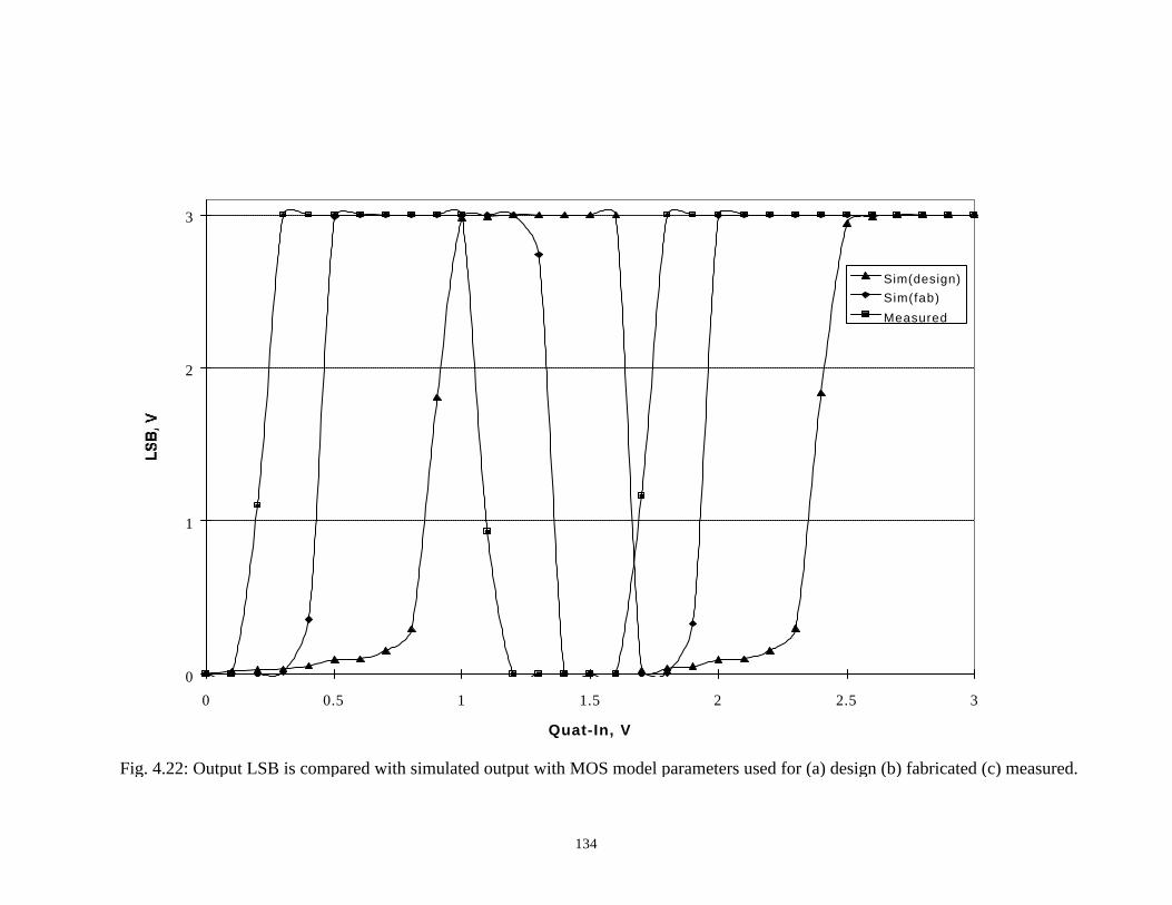
134
Fig. 4.22: Output LSB is compared with simulated output with MOS model parameters used for (a) design (b) fabricated (c) measured.
0
1
2
3
0 0.5 1 1.5 2 2.5 3
Quat-In, V
Sim(design)Sim(fab)
Measured
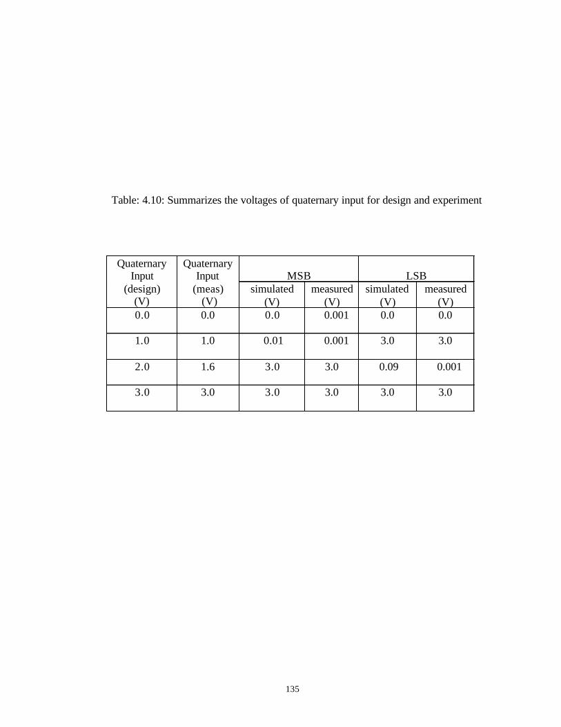
135
Table: 4.10: Summarizes the voltages of quaternary input for design and experiment
MSB
LSB
Quaternary Input
(design) (V)
Quaternary Input
(meas) (V)
simulated (V)
measured (V)
simulated (V)
measured (V)
0.0 0.0 0.0 0.001 0.0 0.0
1.0 1.0 0.01 0.001 3.0 3.0
2.0 1.6 3.0 3.0 0.09 0.001
3.0 3.0 3.0 3.0 3.0 3.0
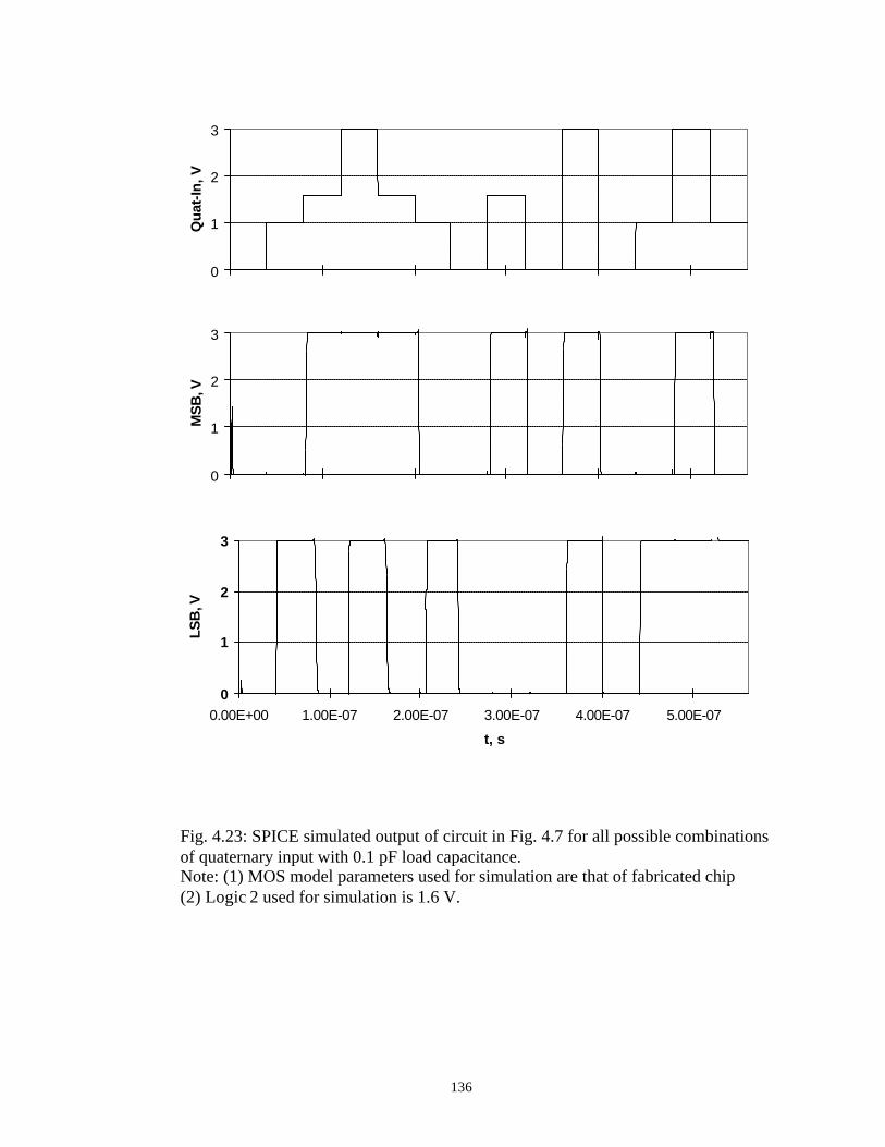
136
Fig. 4.23: SPICE simulated output of circuit in Fig. 4.7 for all possible combinations of quaternary input with 0.1 pF load capacitance. Note: (1) MOS model parameters used for simulation are that of fabricated chip (2) Logic 2 used for simulation is 1.6 V.
0
1
2
3
Qua
t-In
, V
0
1
2
3
MS
B, V
0
1
2
3
0.00E+00 1.00E-07 2.00E-07 3.00E-07 4.00E-07 5.00E-07
t, s
LSB
, V
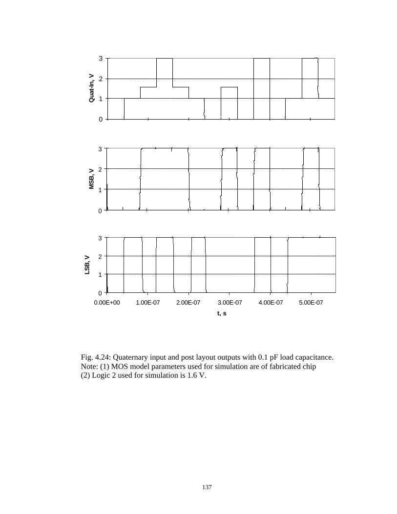
137
Fig. 4.24: Quaternary input and post layout outputs with 0.1 pF load capacitance. Note: (1) MOS model parameters used for simulation are of fabricated chip (2) Logic 2 used for simulation is 1.6 V.
0
1
2
3
Qua
t-In
, V
0
1
2
3
MS
B, V
0
1
2
3
0.00E+00 1.00E-07 2.00E-07 3.00E-07 4.00E-07 5.00E-07
t, s
LSB
, V
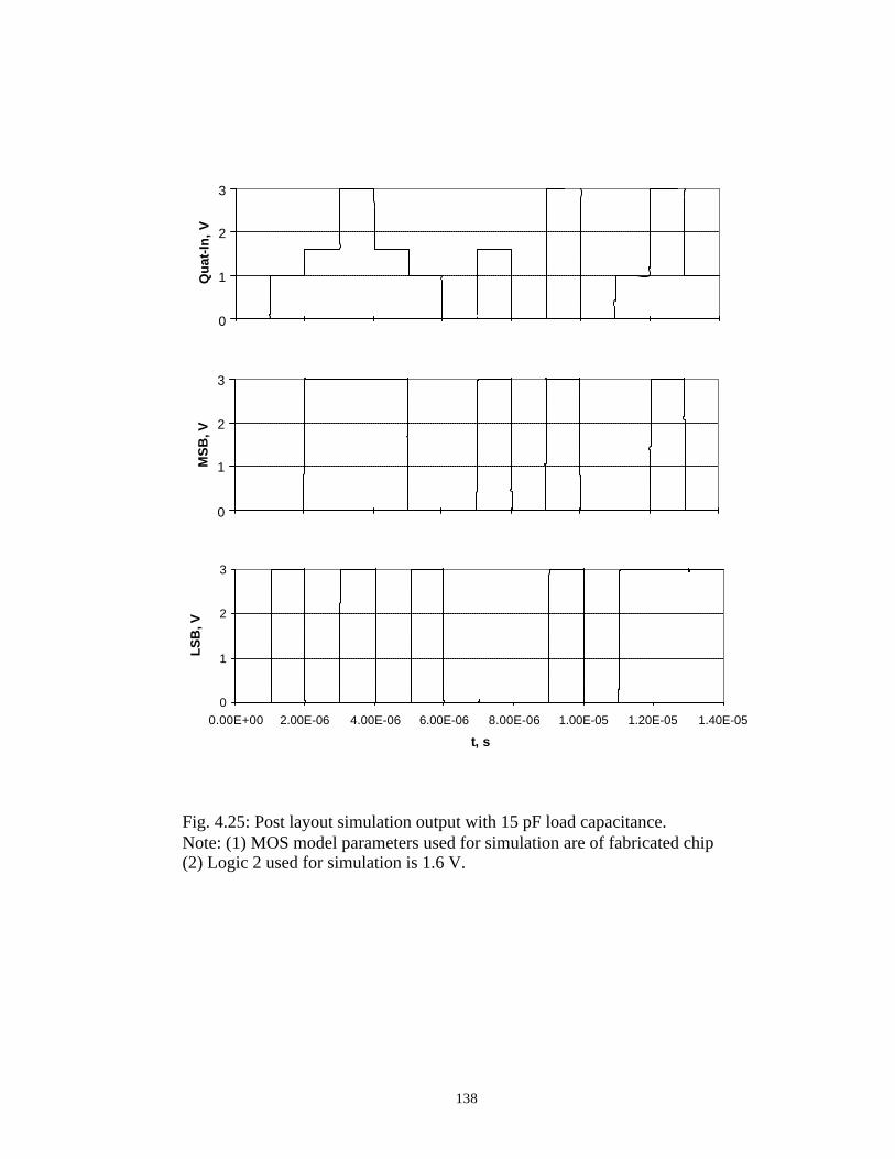
138
Fig. 4.25: Post layout simulation output with 15 pF load capacitance. Note: (1) MOS model parameters used for simulation are of fabricated chip (2) Logic 2 used for simulation is 1.6 V.
0
1
2
3Q
uat-
In, V
0
1
2
3
MS
B, V
0
1
2
3
0.00E+00 2.00E-06 4.00E-06 6.00E-06 8.00E-06 1.00E-05 1.20E-05 1.40E-05
t, s
LSB
, V
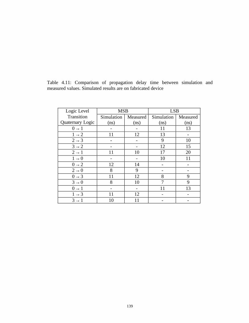
139
Table 4.11: Comparison of propagation delay time between simulation and measured values. Simulated results are on fabricated device
MSB LSB Logic Level Transition
Quaternary Logic Simulation
(ns) Measured
(ns) Simulation
(ns) Measured
(ns) 0→1 - - 11 13 1→2 11 12 13 - 2→3 - - 9 10 3→2 - - 12 15 2→1 11 10 17 20 1→0 - - 10 11 0→2 12 14 - - 2→0 8 9 - - 0→3 11 12 8 9 3→0 8 10 7 9 0→1 - - 11 13 1→3 11 12 - - 3→1 10 11 - -
140
Chapter 5
Conclusion and Future Work
An integrated circuit design is presented for the conversion of ternary bits
into binary bits using multiple- input floating gate MOSFETs. The floating potential
diagrams have been used to design different building blocks of the conversion
circuit. The principle of MIFG transistor, calculating weighted sum of all inputs at
gate level and switching transistor ON or OFF depending upon calculated voltage
greater than or less than switching threshold voltage is utilized. The full integrated
circuit is designed and simulated in standard 1.5 µm digital CMOS technology. The
circuits are simulated in SPICE with MOSIS BSIM3 model parameters. The
physical layout for the circuits is drawn using L-EDIT version 8.2. The post layout
simulations included interlayer and parasitic nodal capacitance to make the
simulation more realistic. The circuits are designed for balanced ternary logic (-1, 0,
+1) unlike previous circuit found in literature, which uses (0, 1, 2) ternary logic.
The output bit maximum propagation delay is 8 ns with 0.1 pF simulated
capacitive load. With 15 pF simulative capacitive load, the output bit maximum
propagation delay is 13 ns. The physical layout of the design occupies an area of
432×908 µm2.
A simple conversion scheme from quaternary to binary bit is also presented
in a standard CMOS process using multiple- input floating gate MOSFETS. The
designed circuit was fabricated in AMI 1.5 µm n-well CMOS process and was
tested for performance. All quaternary logic levels agree with the corresponding
binary bits except the logic 2 (2 V), which was measured at 1.6 V for logic 2 due to
141
possible process variations. The conversion circuit from quaternary logic to binary
logic achieved a great improvement in the number of devices. A reduction of more
than 75% in transistor count was obtained over the previous designs. The circuit can
be easily embedded in digital CMOS design architectures and used in a sensor
readout electronics for transmission of data with reduced bandwidth requirements
over a long distance [47]. The output bit maximum propagation delay is 6 ns with
0.1 pF simulated capacitive load and 17 ns with 15 pF load. The physical layout of
the design occupies an area of 130×175 µm2.
5.1 Future Work
The circuits were designed for conversion from multivalued (ternary and
quaternary) logic to binary logic. An attempt to convert binary logic to multivalued
logic using the multiple-input floating gate MOSFETs can be made. In future, the
work could be extended to convert multivalued logic (radix 8 = 23) to binary logic.
An important aspect of designing circuits using floating gate devices is determining
the value of unit capacitance “C”, which effects the layout area and performance of
the circuit. Thus efforts should be made to determine the optimum value of unit
capacitance that can be implemented.
The practical design aspect of simulating floating gate MOSFET in SPICE
using low-level models is still an issue. Manufactures do not provide models for
simulating floating gate MOSFETs, hence a special technique to simulate these
devices with standard MOS models is required.
142
Bibliography [1] J.T. Butler, Multiple-Valued logic in VLSI, IEEE Computer Society Press
Technology Series, Los Alamitos, CA, 1991. [2] K.C. Smith, “The prospects for multivalued logic: A technology and
applications view,” IEEE Transactions on Computers, vol. C-30, No. 9, September 1981, pp. 619-634.
[3] S.L. Hurst, “Multiple-valued logic – its status and its future,” IEEE
Transactions on Computers, vol. C-33, December 1984, pp. 1160-1179. [4] D.E. Knuth, “The Art of Computer Programming – Volume 2:
Seminumerical Algorithms”, pp.190-192. Addison-Wesley, 2nd ed., 1980. ISBN 0-201-03822-6.
[5] V.C. Hamacher and Z.G. Vranesic, “Multivalued logic in arithmetic units”
in “Computer Science and Multiple valued logic: Theory and Applications”, D.C. Rine Editor, Amsterdam, The Netherlands; North Holland 1977.
[6] T.T. Dao, M. Davio and C. Gossart, “Complex number arithmetic with odd-
valued logic,” IEEE Transactions on Computers, vol. C-26, July 1980, pp. 604-610.
[7] X. W. Wu, “CMOS ternary logic circuits,” IEE Proceedings on Circuits,
Devices and Systems, vol. 137, No. 1, February 1990, pp. 21-27. [8] A. Srivastava and K. Venkatapathy, “Design and implementation of a low
power ternary full adder,” VLSI Design, vol. 4, No. 1, 1996, pp. 75-81. [9] D. Etiemble and M. Israel, “Comparison of binary and multivalued ICs
according to VLSI criteria,” Computer, vol. 21, April 1988, pp. 28-42. [10] K. Wayne Current, “Current-mode CMOS multiple-valued logic circuits,”
IEEE Journal of Solid-State Circuits, vol. 29, No. 2, February 1994, pp. 95-107.
[11] D. Olson and K. W. Current, “Hardware implementation of supplementary
symmetrical logic circuit structure concepts,” Proceedings of 30th International Symposium of Multiple-Valued Logic, May 2000, pp. 371-376.
[12] C. Y. Wu and H. Y. Huang, “Design and application of pipelined dynamic
CMOS ternary logic and simple ternary differential logic,” IEEE Journal of Solid-State Circuits, vol. 28, No. 8, August 1993, pp. 895-906.
143
[13] F. Ueno, T. Inoue, K. Sugitani and Shinji Araki, “A programmable switched- capacitor circuit for multivalued-to-binary and binary-to-multivalued conversions,” Proceedings of International Symposium of Multiple-Valued Logic, 1989, pp. 195-201.
[14] F. Q. Li, M. Morisue and T. Ogata, “A proposal of Josephson binary-to-
ternary converter,” IEEE Transactions on Applied Superconductivity, vol. 5, No. 2, June 1995, pp. 2632-2635.
[15] J. L. Mangin and K. W. Current, “Characteristics of prototype CMOS
quaternary logic encoder-decoder circuits,” IEEE Transactions on Computers, vol. c-35, No. 2, February 1986, pp. 157-161.
[16] N. R. Shanbhag, D. Nagchoudhuri, R. E. Siferd, G. S. Vishweswaran,
“Quaternary logic circuits in 2-µm CMOS technology,” IEEE Journal of Solid-State Circuits, vol. 25, No. 3, June 1990, pp. 790-799.
[17] A. D. Singh, “Four valued buses for clocked CMOS VLSI systems,”
Proceedings of 17th International Symposium of Multiple-Valued Logic, 1987, pp. 128-133.
[18] I. M. Thoidis, D. Soudris, I. Karafyllidis and A. Thanailakis, “The design of
low power multiple-valued logic encoder and decoder circuits,” Proceedings of 6th IEEE International Conference on Electronics, Circuits & Systems, vol. III, September 1999, pp. 1623-1626.
[19] M. Brilman, D. Etiemble, J. L. Oursel and P. Tatareau, “A 4-Valued ECL
encoder and decoder circuit,” IEEE Transactions on Solid-State Circuits, vol. SC-17, No. 3, June 1982, pp. 547-552.
[20] H. G. Kerkhoff and M. L. Tervoert, “Multiple-valued logic charge-coupled
devices,” IEEE Transactions on computers, vol. C-30, No. 9, September 1981, pp. 644-652.
[21] M. H. Abd-El Barr and Z. G. Vranesic, “4-valued 2-attribute encoder/decoder circuits design,” Proceedings of International Symposium of Multiple-Valued Logic, 1985, pp. 323-330.
[22] Y. Guangyu, “High multi-valued digital circuit,” Proceedings of 14th International Symposium of Multiple-Valued Logic, 1984, pp. 173-179.
[23] D. Bhattacharya, “Binary to quaternary encoding in clocked CMOS circuits using weak buffers,” Proceedings of 20th International Symposium of Multiple-Valued Logic, 1990, pp. 174-180.
144
[24] D. M. Garner, L. Sabesan, G. A. J. Amartunga, A. Blackburn, J. Clark, S.S. Sekiariapuram and A. G. R. Evans, “ A novel flash EEPROM cell based on trench technology for integration within power integrated circuits,” IEEE Electron Device Letters, vol. 21, No. 5, May 2000, pp. 236-238.
[25] S. S. Chung, C. M. Yih, S. T. Liaw, Z. H. Ho, S.S. Wu, C. J. Lin, D. S. Kuo,
and M. S. Liang, “A novel high performance and reliability p-type floating gate N-channel flash EEPROM,” IEEE Symposium on VLSI Technology, June 1999, pp. 19-20.
[26] K. H. Wee, T. Nozawa, T. Yonezawa, Y. Yamashita, T. Shibata and T.
Ohmi, “High-precision analog EEPROM with real-time write monitoring,” IEEE International Symposium on Circuits and Systems, May 2001, pp. 105-108.
[27] J. Ramirez-Angulo and A. J. Lopez, “MITE circuits: the continous-time
counterpart to switched-capacitor circuits,” IEEE Transactions on Circuits and Systems-II: Analog and Digital Signal Processing, vol. 48, No. 1, January, 2001, pp. 45-55.
[28] P. Hasler, “Continuous-time feedback in floating-gate MOS circuits,” IEEE
Transactions on Circuits and Systems-II: Analog and Digital Signal Processing, vol. 48, No. 1, January, 2001, pp. 56-64.
[29] R. R. Harrison, J. A. Bragg, P. Hasler, B. A. Minch and S. P. Deweerth,” A
CMOS programmable analog memory-cell array using floating-gate circuits,” IEEE Transactions on Circuits and Systems-II: Analog and Digital Signal Processing, vol. 48, No. 1, January, 2001, pp. 4-11.
[30] K. Ogawa, T. Shibata, T. Ohmi, M. Takatsu and N. Yokoyama, “Multiple-
input neuron MOS operational amplifier for voltage-mode multivalued full adders,” IEEE Transactions on Circuits and Systems-II: Analog and Digital Signal Processing, vol. 45, No. 9, September, 1998, pp. 1307-1311.
[31] W. Weber, S. Prange, R. Thewes and E. Wohlrab, “A neuron MOS
transistor-based multiplier cell,” in IEDM Technical Digest, 1995, pp. 21.5.1-21.5.4.
[32] T. Shibata and T. Ohmi, “An intelligent MOS transistor featuring gate- level
weighted sum and threshold operations,” in IEDM Tech. Dig., 1991, pp. 919-922.
[33] T. Shibata and T. Ohmi, “A functional MOS transistor featuring gate- level
weighted sum and threshold operations,” IEEE Transactions on Electron devices, vol. 39, No. 6, June 1992, pp. 1444-1455.
145
[34] A. Luck, S. Jung, R. Brederlow, R. Thewes, K. Goser and W. Weber, “On the design robustness of threshold logic gates using multi- input floating gate MOS transistors,” IEEE Transactions on Electron Devices, vol. 47, No. 6, June 2000, pp. 1231-1239.
[35] W. Weber, S. J. Prange, R. Thewes, E. Wohlrab and A. Luck, “On the
application of the neuron MOS transistor principle for modern VLSI design,” IEEE Transactions on Electron Devices, vol. 43, No. 10, October 1996, pp. 1700-1708.
[36] T. Shibata and T. Ohmi, “Neuron MOS binary- logic integrated circuits part
I: design fundamentals and soft hardware-logic circuit implementation,” IEEE Transactions on Electron Devices, vol. 40, No. 3, March 1993, pp. 570-576.
[37] T. Shibata and T. Ohmi, “Neuron MOS binary- logic integrated circuits part
II: simplifying techniques of circuit configuration and their practical applications,” IEEE Transactions on Electron Devices, vol. 40, No. 5, May 1993, pp. 974-979.
[38] N. H. E. Weste and K. Eshragian, “Principle of CMOS VLSI Design, A
system perspective,” Addison-Wesley, CA 1993, ISBN:0201533766 . [39] A. Thomsen and M. A. Brooke, “A floating gate MOSFET with tunneling
injector fabricated using a standard double-polysilicon CMOS process,” IEEE Electron Device Letters, vol. 12, No. 3. March 1991, pp. 111-113.
[40] B. A. Minch and P. Hasler, “A floating-gate technology for digital CMOS
process,” Proceedings of International Symposium of Circuit and Systems, vol. II, 1999, pp. 400-403.
[41] Y. Tsividis, “Mixed Analog-Digital VLSI Devices and Technology: An
Introduction,” McGraw- Hill, New York, 1996, pp. 220-225, ISBN: 0070654026.
[42] K. Kotani, T. Shibata, M. Imai and T. Ohmi, “Clock-controlled Neuron-
MOS logic gates,” IEEE Transactions on Circuits and Systems-II: Analog and Digital Signal Processing, vol. 45, No. 4, April, 1998, pp. 518-522.
[43] M. Renovell, “Electrical analysis and modeling of floating-gate fault,” IEEE
Transactions on Computer-Aided Design, vol. 11, No. 11, November 1992, pp. 1450-1458.
[44] J. Ramirez-Angulo, G. Gonzalez-Altamirano and S.C. Choi, “Modeling
multiple- input floating gate transistors for analog signal processing,” IEEE International Symposium on Circuit and Systems, 1997, pp. 2020-2023.
146
[45] L.Yin, S.H.K. Embabi and E. Sanchez-Sinencio, “A floating gate MOSFET
D/A converter,” in IEEE International Symposium on Circuit and Systems, 1997, pp. 409-412.
[46] E. R. Villegas, G. Huertas, M. J. Avedillo, J. M. Quintana and A. Rueda, “A
practical floating-gate muller-C element using vMOS threshold gates,” IEEE Transactions on Circuits and Sytems-II: Analog and Digital Signal Processing, vol. 48, No. 1, January 2001, pp. 102-105.
[47] A. Srivastava, H. N. Venkata, P. K. Ajmera, “A novel scheme for a higher
bandwidth sensor readout,” Proceedings SPIE, vol. 4700, pp. 17-28.

147
Appendix A Input Circuit Files * Circuit file to obtain the I-V Characteristics of floating gate nMOS transistor. * B2 Spice default format (same as Berkeley Spice 3F format) M1 1 2 0 0 Bsim3_05_nmos l = 1.6u w = 4.0u C2 2 3 500ff * Drain to Source voltage (PWL) V3 1 0 DC 3V PWL (0ns 0v 300ns 3V) * Different Gate to Source voltages V4 3 0 DC 0 *V4 3 0 DC 1 *V4 3 0 DC 1.5 *V4 3 0 DC 2 *V4 3 0 DC 2.5 *V4 3 0 DC 3 .model Bsim3_05_nmos nmos (BSIM3 level parameters used shown in Appendix B) .OPTIONS gmin = 1E-12 reltol = 1E-4 itl1 = 500 itl4 = 500 + rshunt = 100G .TRAN 1ns 300ns 0 1ns uic .IC .END

148
* Circuit file used to obtain the I-V Characteristics of floating gate pMOS transistor * B2 Spice default format (same as Berkeley Spice 3F format) M1 1 2 0 0 Bsim3_05_pmos l = 1.6u w = 4.0u C2 2 3 500ff * Drain to Source voltage (PWL) V3 1 0 DC 3V PWL (0ns 0v 300ns -3V) * Different Gate to Source voltages V4 3 0 DC 0 *V4 3 0 DC -1 *V4 3 0 DC -1.5 *V4 3 0 DC -2 *V4 3 0 DC -2.5 *V4 3 0 DC -3 .model Bsim3_05_pmos pmos (BSIM3 level parameters used shown in Appendix B) .OPTIONS gmin = 1E-12 reltol = 1E-4 itl1 = 500 itl4 = 500 + rshunt = 100G .TRAN 1ns 300ns 0 1ns uic .IC .END

149
* Circuit file to obtain the Transfer Curve for the nMOS floating gate transistor * B2 Spice default format (same as Berkeley Spice 3F format) M3 1 2 0 0 Bsim3_05_nmos l = 1.6u w = 4.0u C3 2 3 500ff * Gate to Source voltage V5 3 0 DC 1 PWL ( 0ns –2v 500ns 3v) *Different Drain to Source voltage V6 1 0 DC 1V * V6 1 0 DC 2V *V6 1 0 DC 3V .model Bsim3_05_nmos nmos (BSIM3 level parameters used shown in Appendix B) .OPTIONS gmin = 1E-12 reltol = 1E-4 itl1 = 500 itl4 = 500 + rshunt = 100G .TRAN 1ns 500ns 0 1ns uic .IC .END
150
* Circuit file used to obtain the Transfer Curve of floating gate pMOS transistor * B2 Spice default format (same as Berkeley Spice 3F format) M1 1 2 0 1 Bsim3_pmos l = 1.6u w = 4.0u C2 2 3 500ff *Gate to Source Voltage V2 3 0 DC -1 PWL ( 0ns 2v 500ns -3v) * Different Drain to Source Voltage V3 1 0 DC -1V *V3 1 0 DC -2V *V3 1 0 DC -3V .model Bsim3_pmos pmos (BSIM3 level parameters used shown in Appendix B) .OPTIONS gmin = 1E-12 reltol = 1E-4 itl1 = 500 itl4 = 500 + rshunt = 100G .TRAN 1ns 500ns 0 1ns uic .IC .END

151
* Circuit file to obtain the voltage transfer characteristics of floating gate CMOS inverter * with various capacitors as shown in Fig. 2.14 * B2 Spice default format (same as Berkeley Spice 3F format) M1 5 4 0 0 Bsim3_05_nmos l = 1.6u w = 8.0u M2 5 4 22 22 Bsim3_pmos l = 1.6u w = 8.0u C1 6 4 500ff * Supply Voltage VDD V1 22 0 DC 3V * Gate voltage Vin V2 6 0 DC 3 PWL ( 0ns 0v 120ns 3v) *other capacitors used for obtaining the curves *C6 0 4 20ff *C7 0 4 40ff *C8 22 4 20ff *C9 22 4 40ff *output node : 5 .OPTIONS gmin = 1E-12 reltol = 1E-4 itl1 = 500 itl4 = 500 + rshunt = 100G .TRAN 1ns 120ns 0 1ns uic .IC .END

152
Appendix B
Design MOSFET Model Parameters
nMOS Model Parameters .MODEL NMOS NMOS ( LEVEL = 49 +VERSION = 3.1 TNOM = 27 TOX = 1.41E-8 +XJ = 1.5E-7 NCH = 1.7E17 VTH0 = 0.6783469 +K1 = 0.8198806 K2 = -0.0815723 K3 = 21.2872824 +K3B = -8.3769938 W0 = 1E-8 NLX = 1E-9 +DVT0W = 0 DVT1W = 0 DVT2W = 0 +DVT0 = 2.9769564 DVT1 = 0.4298091 DVT2 = -0.1314503 +U0 = 459.4465085 UA = 1E-13 UB = 1.566796E-18 +UC = 1.344E-11 VSAT = 1.676264E5 A0 = 0.5671021 +AGS = 0.1157472 B0 = 2.856769E-6 B1 = 5E-6 +KETA = -3.548797E-3 A1 = 5.378248E-4 A2 = 0.3584167 +RDSW = 1.421987E3 PRWG = 0.0206332 PRWB = 0.0174913 +WR = 1 WINT = 2.860502E-7 LINT = 3.762151E-8 +XL = 0 XW = 0 DWG = -1.572821E-8 +DWB = 3.973063E-8 VOFF = 0 NFACTOR = 0.9112552 +CIT = 0 CDSC = 2.4E-4 CDSCD = 0 +CDSCB = 0 ETA0 = 0.0428326 ETAB = -1.388924E-3 +DSUB = 0.317372 PCLM = 2.4796867 PDIBLC1 = -0.5457422 +PDIBLC2 = 2.946108E-3 PDIBLCB = -8.49120E-3 DROUT = 0.726107 +PSCBE1 = 5.402825E8 PSCBE2 = 3.692234E-5 PVAG = 9.248005E-3 +DELTA = 0.01 RSH = 83 MOBMOD = 1 +PRT = 0 UTE = -1.5 KT1 = -0.11 +KT1L = 0 KT2 = 0.022 UA1 = 4.31E-9 +UB1 = -7.61E-18 UC1 = -5.6E-11 AT = 3.3E4 +WL = 0 WLN = 1 WW = 0 +WWN = 1 WWL = -6.554e-20 LL = 0 +LLN = 1 LW = 0 LWN = 1 +LWL = -9.461E-20 CAPMOD = 2 XPART = 0.5 +CGDO = 2.2E-10 CGSO = 2.2E-10 CGBO = 1E-9 +CJ = 4.188753E-4 PB = 0.99 MJ = 0.4464981 +CJSW = 3.196259E-10 PBSW = 0.1 MJSW = 0.1128874 +CJSWG = 1.64E-10 PBSWG = 0.1 MJSWG = 0.1128874 +CF = 0 PVTH0 = -0.0848114 PRDSW = -400.6457406 +PK2 = -0.0250774 WKETA = -0.0208937 LKETA = 2.577922E-3 )

153
pMOS Model Parameters .MODEL PMOS PMOS ( LEVEL = 49 +VERSION = 3.1 TNOM = 27 TOX = 1.41E-8 +XJ = 1.5E-7 NCH = 1.7E17 VTH0 = -0.9341243 +K1 = 0.5370998 K2 = -0.0122252 K3 =3.7496262 +K3B = -0.9286477 W0 = 6.54045E-8 NLX = 1E-9 +DVT0W = 0 DVT1W = 0 DVT2W = 0 +DVT0 = 2.9562583 DVT1 = 0.5245313 DVT2 = -0.0997267 +U0 = 237.0052372 UA = 3.45997E-9 UB = 1E-21 +UC =-5.45512E-11 VSAT = 2E5 A0 = 0.8887791 +AGS = 0.1458591 B0 = 1.07758E-6 B1 = 5E-6 +KETA = -2.767583E-3 A1 = 0 A2 = 0.3 +RDSW = 2.565262E3 PRWG = -0.0526966 PRWB = -0.0674531 +WR = 1 WINT = 3.631054E-7 LINT = 3.573418E-8 +XL = 0 XW = 0 DWG = -3.251632E-8 +DWB = 1.114661E-8 VOFF = -0.046905 NFACTOR = 0.9565103 +CIT = 0 CDSC = 2.4E-4 CDSCD = 0 +CDSCB = 0 ETA0 = 3.183212E-4 ETAB = 2.302539E-5 +DSUB = 0.0150846 PCLM = 2.4099721 PDIBLC1 = -0.1320417 +PDIBLC2 = 2.588158E-3 PDIBLCB = -0.0999382 DROUT = 0.3140708 +PSCBE1 =7.275362E9 PSCBE2 = 7.138855E-10 PVAG = 0.5287847 +DELTA = 0.01 RSH = 105.1 MOBMOD = 1 +PRT = 0 UTE = -1.5 KT1 = -0.11 +KT1L = 0 KT2 = 0.022 UA1 = 4.31E-9 +UB1 = -7.61E-18 UC1 = -5.6E-11 AT = 3.3E4 +WL = 0 WLN = 1 WW = 0 +WWN = 1 WWL = -1.205E-20 LL = 0 +LLN = 1 LW = 0 LWN = 1 +LWL = 6.268E-21 CAPMOD = 2 XPART = 0.5 +CGDO = 2.36E-10 CGSO = 2.36E-10 CGBO = 1E-9 +CJ = 7.230164E-4 PB = 0.9520106 MJ = 0.4950624 +CJSW = 2.598254E-10 PBSW = 0.99 MJSW = 0.2998526 +CJSWG = 6.4E-11 PBSWG = 0.1 MJSWG = 0.1245165 +CF = 0 PVTH0 = 5.98016E-3 PRDSW = 14.8598424 +PK2 = 3.73981E-3 WKETA = 4.758951E-3 LKETA = -3.900197E-3 )
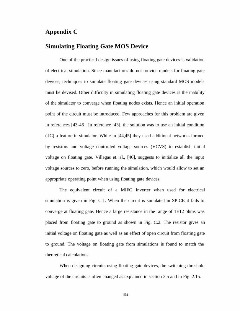
154
Appendix C
Simulating Floating Gate MOS Device
One of the practical design issues of using floating gate devices is validation
of electrical simulation. Since manufactures do not provide models for floating gate
devices, techniques to simulate floating gate devices using standard MOS models
must be devised. Other difficulty in simulating floating gate devices is the inability
of the simulator to converge when floating nodes exists. Hence an initial operation
point of the circuit must be introduced. Few approaches for this problem are given
in references [43-46]. In reference [43], the solution was to use an initial condition
(.IC) a feature in simulator. While in [44,45] they used additional networks formed
by resistors and voltage controlled voltage sources (VCVS) to establish initial
voltage on floating gate. Villegas et. al., [46], suggests to initialize all the input
voltage sources to zero, before running the simulation, which would allow to set an
appropriate operating point when using floating gate devices.
The equivalent circuit of a MIFG inverter when used for electrical
simulation is given in Fig. C.1. When the circuit is simulated in SPICE it fails to
converge at floating gate. Hence a large resistance in the range of 1E12 ohms was
placed from floating gate to ground as shown in Fig. C.2. The resistor gives an
initial voltage on floating gate as well as an effect of open circuit from floating gate
to ground. The voltage on floating gate from simulations is found to match the
theoretical calculations.
When designing circuits using floating gate devices, the switching threshold
voltage of the circuits is often changed as explained in section 2.5 and in Fig. 2.15.
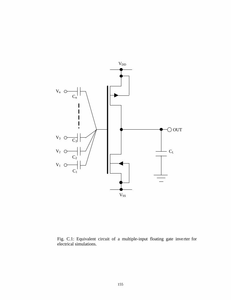
155
Fig. C.1: Equivalent circuit of a multiple-input floating gate inverter for electrical simulations.
Vn
OUT
CL
VDD
VSS
V3
V2
V1
C1
C2
C3
Cn
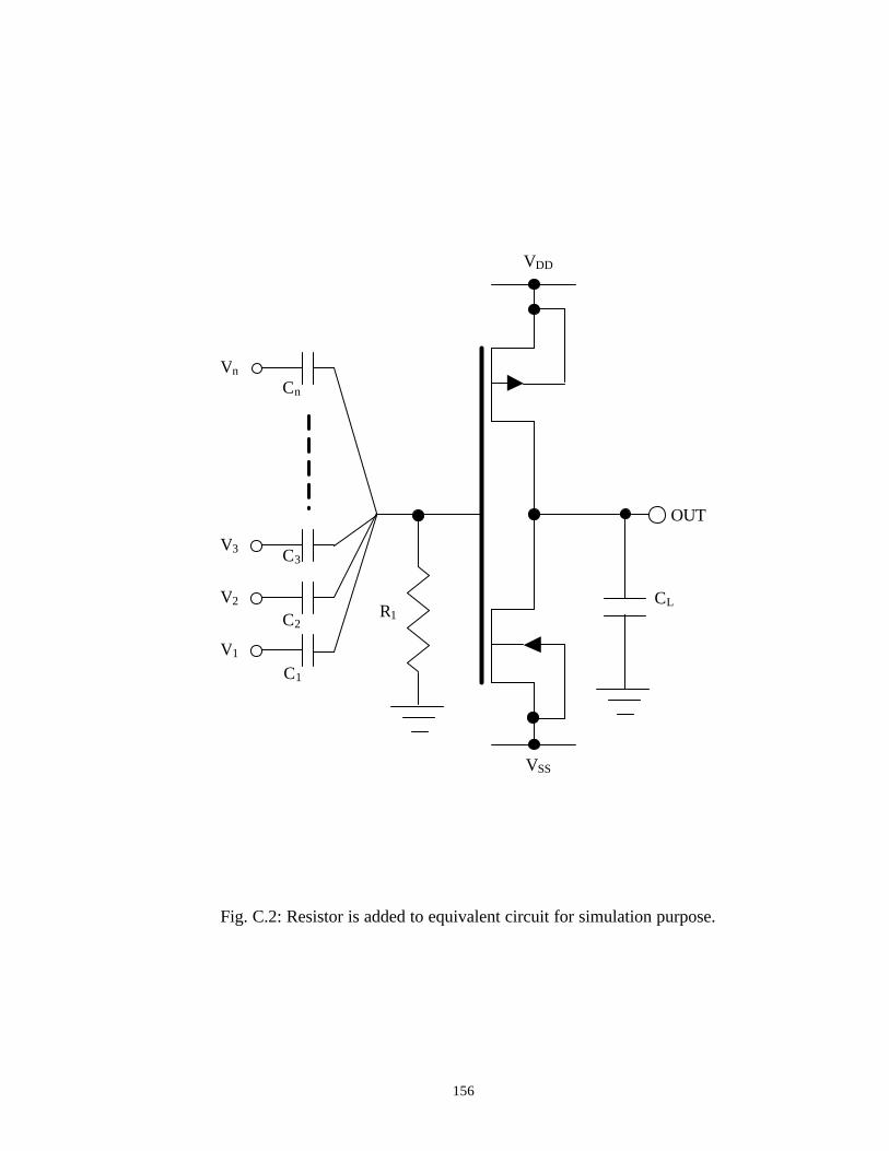
156
Fig. C.2: Resistor is added to equivalent circuit for simulation purpose.
Vn
OUT
CL
VDD
VSS
V3
V2
V1
C1
C2
C3
Cn
R1
157
When capacitor C1 is used with DC voltage source as input to the
capacitance, the simulator recognizes it as a DC storage capacitor, instead of a AC
coupling capacitance and blocks the voltage. The DC voltage source is replaced
with a piece-wise-linear voltage source by using which the simulator simulates the
capacitor as a coupling capacitance. Taken the above considerations for simulating
circuits having floating gate devices, the experimental results of circuits failed when
MIFG inverters were cascaded.
The circuits are simulated in B2 SPICE with MOSIS BSIM3 MOS model
parameters. The B2 SPICE uses an option RSHUNT = 100 G, which places a
resistor of 1E11 from every node in the circuit to ground. Thus giving an open
circuit effect and as well avoiding floating nodes in the circuit.
158
Appendix D
MOSFET Model Parameters of the Fabricated Chip
nMOS Model Parameters for 1.5-µm technology (T1AZ) .MODEL NMOS NMOS ( LEVEL = 8 +VERSION = 3.1 TNOM = 27 TOX = 3.07E-8 +XJ = 3E-7 NCH = 7.5E16 VTH0 = 0.5946428 +K1 = 0.9317355 K2 = -0.0642401 K3 = 8.1988053 +K3B = -1.6036239 W0 = 1E-7 NLX = 1E-8 +DVT0W = 0 DVT1W = 0 DVT2W = 0 +DVT0 = 0.6287112 DVT1 = 0.3396 DVT2 = -0.3380439 +U0 = 690.3302409 UA = 2.107409E-9 UB = 1.45864E-18 +UC = 5.597668E-11 VSAT = 1.101194E5 A0 = 0.6538174 +AGS = 0.1405777 B0 = 2.36604E-6 B1 = 5E-6 +KETA = -5.491058E-3 A1 = 0 A2 = 1 +RDSW = 3E3 PRWG =-0.0257109 PRWB = -0.0343409 +WR = 1 WINT = 7.640524E-7 LINT = 2.383339E-7 +XL = 0 XW = 0 DWG = -2.045861E-8 +DWB = 3.86526E-8 VOFF = -0.052426 NFACTOR = 0.7700134 +CIT = 0 CDSC = 0 CDSCD = 2.966891E-6 +CDSCB = 5.248867E-5 ETA0 = -1 ETAB = -0.4998094 +DSUB = 1 PCLM = 1.1865082 PDIBLC1 = 7.872555E-3 +PDIBLC2 = 1.779838E-3 PDIBLCB = -0.1 DROUT = 0.0559194 +PSCBE1 = 2.6186E9 PSCBE2 = 5.988929E-10 PVAG = 0.2015173 +DELTA = 0.01 RSH = 51.8 MOBMOD = 1 +PRT = 0 UTE = -1.5 KT1 = -0.11 +KT1L = 0 KT2 = 0.022 UA1 = 4.31E-9 +UB1 = -7.61E-18 UC1 = -5.6E-11 AT = 3.3E4 +WL = 0 WLN = 1 WW = 0 +WWN = 1 WWL = 0 LL = 0 +LLN = 1 LW = 0 LWN = 1 +LWL = 0 CAPMOD = 2 XPART = 0.5 +CGDO = 1.75E-10 CGSO = 1.75E-10 CGBO = 1E-9 +CJ = 2.922743E-4 PB = 0.9688488 MJ = 0.5144895 +CJSW = 1.31563E-10 PBSW = 0.99 MJSW = 0.1 +CJSWG = 6.4E-11 PBSWG=0.99 MJSWG=0.1 +CF = 0 )
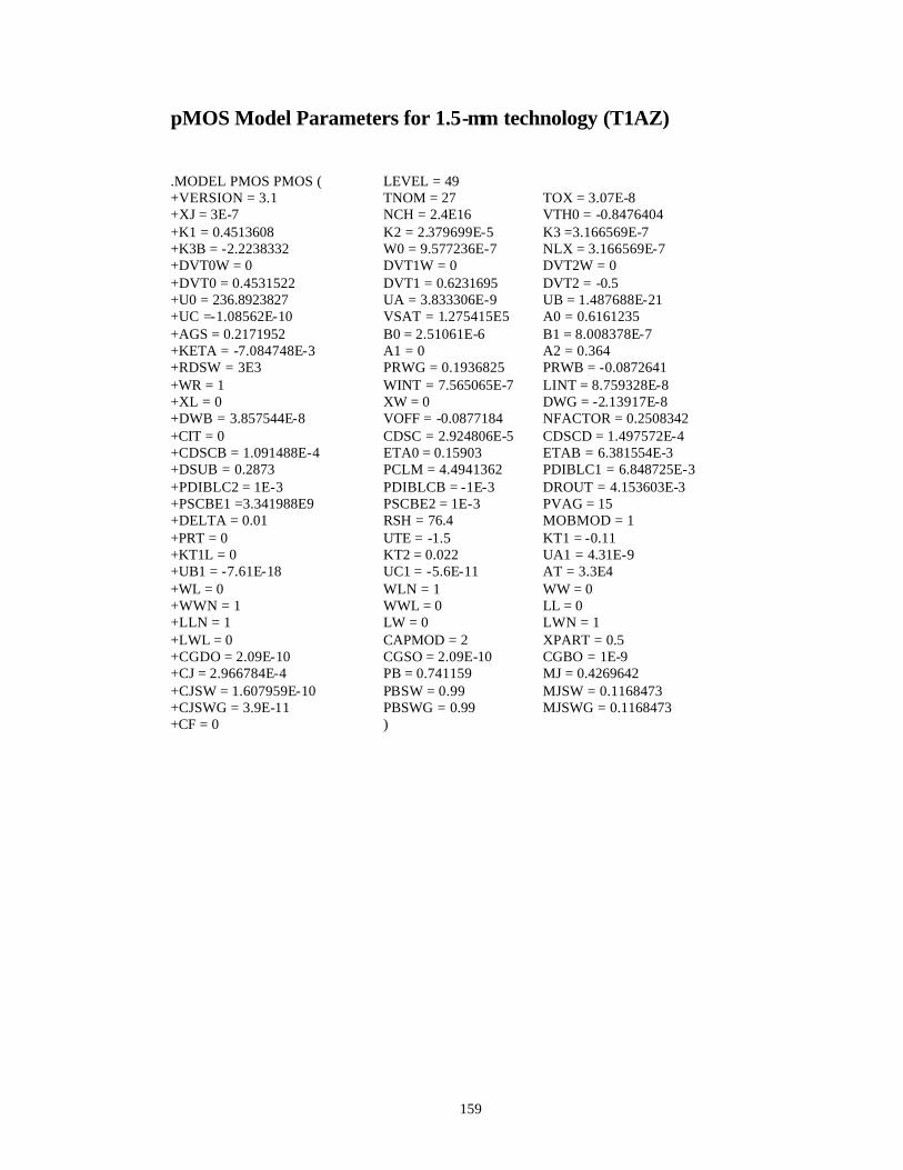
159
pMOS Model Parameters for 1.5-µm technology (T1AZ) .MODEL PMOS PMOS ( LEVEL = 49 +VERSION = 3.1 TNOM = 27 TOX = 3.07E-8 +XJ = 3E-7 NCH = 2.4E16 VTH0 = -0.8476404 +K1 = 0.4513608 K2 = 2.379699E-5 K3 =3.166569E-7 +K3B = -2.2238332 W0 = 9.577236E-7 NLX = 3.166569E-7 +DVT0W = 0 DVT1W = 0 DVT2W = 0 +DVT0 = 0.4531522 DVT1 = 0.6231695 DVT2 = -0.5 +U0 = 236.8923827 UA = 3.833306E-9 UB = 1.487688E-21 +UC =-1.08562E-10 VSAT = 1.275415E5 A0 = 0.6161235 +AGS = 0.2171952 B0 = 2.51061E-6 B1 = 8.008378E-7 +KETA = -7.084748E-3 A1 = 0 A2 = 0.364 +RDSW = 3E3 PRWG = 0.1936825 PRWB = -0.0872641 +WR = 1 WINT = 7.565065E-7 LINT = 8.759328E-8 +XL = 0 XW = 0 DWG = -2.13917E-8 +DWB = 3.857544E-8 VOFF = -0.0877184 NFACTOR = 0.2508342 +CIT = 0 CDSC = 2.924806E-5 CDSCD = 1.497572E-4 +CDSCB = 1.091488E-4 ETA0 = 0.15903 ETAB = 6.381554E-3 +DSUB = 0.2873 PCLM = 4.4941362 PDIBLC1 = 6.848725E-3 +PDIBLC2 = 1E-3 PDIBLCB = -1E-3 DROUT = 4.153603E-3 +PSCBE1 =3.341988E9 PSCBE2 = 1E-3 PVAG = 15 +DELTA = 0.01 RSH = 76.4 MOBMOD = 1 +PRT = 0 UTE = -1.5 KT1 = -0.11 +KT1L = 0 KT2 = 0.022 UA1 = 4.31E-9 +UB1 = -7.61E-18 UC1 = -5.6E-11 AT = 3.3E4 +WL = 0 WLN = 1 WW = 0 +WWN = 1 WWL = 0 LL = 0 +LLN = 1 LW = 0 LWN = 1 +LWL = 0 CAPMOD = 2 XPART = 0.5 +CGDO = 2.09E-10 CGSO = 2.09E-10 CGBO = 1E-9 +CJ = 2.966784E-4 PB = 0.741159 MJ = 0.4269642 +CJSW = 1.607959E-10 PBSW = 0.99 MJSW = 0.1168473 +CJSWG = 3.9E-11 PBSWG = 0.99 MJSWG = 0.1168473 +CF = 0 )
160
Vita
Harish Naga Venkata was born on November 30, 1977, in Hyderabad, India.
He received his Bachelor of Technology in Electronics and Communication
Engineering degree from Sri Venkateswara University, Tirupati, India, in May,
1999. He was enrolled in the Department of Electrical and Computer Engineering at
Louisiana State University, Baton Rouge, Louisiana, to attend graduate school. He
is presently working for Micron Technology Inc., Allen, Texas. His research
interests include multivalued logic, multiple input- floating gate MOSFETs,
capacitive based architectures.
Related Documents


![Ternary Logic Gates and Ternary SRAM Cell ….pdf · According to blueprint of Weste & Harris in [4] for design of a binary SRAM, a ternary SRAM is constructed similarly. A ternary](https://static.cupdf.com/doc/110x72/5a8290bb7f8b9aa24f8e2227/ternary-logic-gates-and-ternary-sram-cell-pdfaccording-to-blueprint-of-weste.jpg)