Temperature Evolution of Spin-Polarized Electron Tunneling in Silicon Nanowire–Permalloy Lateral Spin Valve System Jean Tarun 1;2 , Shaoyun Huang 1 , Yasuhiro Fukuma 1 , Hiroshi Idzuchi 1;5 , YoshiChika Otani 1;5 , Naoki Fukata 4 , Koji Ishibashi 1;3 , and Shunri Oda 2 1 Advanced Science Institute, RIKEN, Wako, Saitama 351-0198, Japan 2 Quantum Nanoelectronics Research Center and Department of Physical Electronics, Tokyo Institute of Technology, Meguro, Tokyo 152-8552, Japan 3 Interdisciplinary Graduate School of Science and Technology, Tokyo Institute of Technology, Yokohama 226-8503, Japan 4 International Center for Materials Nanoarchitectonics, National Institute for Materials Science, Tsukuba, Ibaraki 305-0044, Japan 5 Institute for Solid State Physics, University of Tokyo, Kashiwa, Chiba 277-8581, Japan Received January 30, 2012; accepted February 22, 2012; published online March 16, 2012 A huge nonlocal spin valve signal over 700 has been observed in silicon-nanowire-based lateral spin valve with permalloy electrodes. The magnitude of the observed huge spin signal was quantitatively explained using the conventional spin diffusion model in a one-dimensionally confined silicon channel. From the temperature dependence of the spin signal, the interface spin polarization was found to be strongly depolarized by raising the temperature. This special characteristic can be reasonably explained by considering an increase in the tunneling of thermally activated electrons through the Schottky barrier with an extremely thin depletion layer. # 2012 The Japan Society of Applied Physics T he combination of nanoelectronics and electron– spin degrees of freedom is a promising approach for overcoming the fundamental limit of downscaling in semiconductor devices. Numerous devices utilizing nonvolatile spin functionalities such as spin field-effect transistor (FET), 1) spin metal–oxide–semiconductor (MOS) FET, 2) and hot-electron spin transistors 3) have been pro- posed. In order to realize such semiconductor spin devices, efficient electrical spin injection and detection are key ingredients. Significant developments in spin injection into semiconductors have been achieved by employing a highly resistive tunnel barrier at the ferromagnetic metal (FM)/ semiconductor interface. 3–8) In their experiments, creation of the spin accumulation in a semiconductor channel has been verified by nonlocal spin valve 3–6) or Hanle 6–8) spin precession measurements. However, the device structures reported 3–9) so far consist of FM electrodes with large lateral dimensions over several m on bulk or thin-film silicon (Si) channels, which are far from the realistic dimensions in the practical nanoelectronic devices. For the semiconductor channel, we focus on a silicon nanowire (SiNW), which enables easy access to the miniaturization of a MOSFET. Moreover, the enhancement of the spin accumulation is expected in a SiNW because of the weak spin–orbit interac- tion, the elastic scattering at the side edge, and the quasi- one-dimensional confinement in the SiNW. 10) We previously reported on nonlocal spin injection into SiNWs using cobalt (Co) leads. 11) However, the large grain size and poor oxida- tion resistance of the Co electrode make it difficult to study the spin transport in SiNWs systematically. In the present work, permalloy (Py: Ni 80 Fe 20 ) was used for the ferromag- netic contact in view of its negligible magnetostriction and its relatively high stability against oxidation as compared with Co. 12) Here, we investigate the temperature dependence of the nonlocal spin signal in a SiNW-based lateral spin valve with secure Py/SiNW interfaces. The n-type h111i-oriented SiNWs with plausible carrier concentration 5{7 10 19 cm 3 were grown by the gold- nanocatalyst-mediated chemical vapor deposition method, and transferred on a Si substrate with a 200-nm-thick SiO 2 top layer. To make a multiterminal lateral spin valve structure based on SiNW, two-step electron-beam lithog- raphy and liftoff processes were carried out. Details of the device fabrication process have been described pre- viously. 11) Figure 1 shows a scanning electron micrograph of a representative lateral spin valve device consisting of nonmagnetic Ti/Au (5 nm/80 nm) electrodes (C1 and C4) and Py (80 nm) spin injector (C2) and detector (C3), which are connected via the 40-nm-diameter SiNW. The Py elec- trodes were covered by a 5-nm-thick MgO capping layer in order to prevent surface oxidation. The center-to-center separation (d) between the Py injector and detector was 1250 nm. Since the Py injector and detector have different edge shapes, their magnetization configuration can be controlled by simply adjusting the external magnetic field along the Py wires. 13) Spin transport properties in the SiNW were evaluated by the nonlocal spin valve measurement, where the charge-current-induced spurious effects can be eliminated. 14) Spin-polarized electrons were injected into the SiNW by biasing C2 and C1 with an ac excitation current of 3 nA, and the voltage difference between C3 and C4 was Fig. 1. Representative SEM image of the multiterminal SiNW lateral spin valve device. In the nonlocal measurement geometry (green labels), spin- polarized current injection uses C2 and C1 contacts, while the nonlocal voltage is measured across C3 and C4. The distance between C2 and C3 varies depending on the length of the SiNW. The additional artifacts (dust) seen on the SEM image are due to handling prior SEM, and not intrinsic to the device. E-mail address: [email protected] Applied Physics Express 5 (2012) 045001 045001-1 # 2012 The Japan Society of Applied Physics DOI: 10.1143/APEX.5.045001

Welcome message from author
This document is posted to help you gain knowledge. Please leave a comment to let me know what you think about it! Share it to your friends and learn new things together.
Transcript
Temperature Evolution of Spin-Polarized Electron Tunneling
in Silicon Nanowire–Permalloy Lateral Spin Valve System
Jean Tarun1;2, Shaoyun Huang1�, Yasuhiro Fukuma1, Hiroshi Idzuchi1;5,
YoshiChika Otani1;5, Naoki Fukata4, Koji Ishibashi1;3, and Shunri Oda2
1Advanced Science Institute, RIKEN, Wako, Saitama 351-0198, Japan2Quantum Nanoelectronics Research Center and Department of Physical Electronics, Tokyo Institute of Technology,
Meguro, Tokyo 152-8552, Japan3Interdisciplinary Graduate School of Science and Technology, Tokyo Institute of Technology, Yokohama 226-8503, Japan4International Center for Materials Nanoarchitectonics, National Institute for Materials Science, Tsukuba, Ibaraki 305-0044, Japan5Institute for Solid State Physics, University of Tokyo, Kashiwa, Chiba 277-8581, Japan
Received January 30, 2012; accepted February 22, 2012; published online March 16, 2012
A huge nonlocal spin valve signal over 700� has been observed in silicon-nanowire-based lateral spin valve with permalloy electrodes. The
magnitude of the observed huge spin signal was quantitatively explained using the conventional spin diffusion model in a one-dimensionally
confined silicon channel. From the temperature dependence of the spin signal, the interface spin polarization was found to be strongly depolarized
by raising the temperature. This special characteristic can be reasonably explained by considering an increase in the tunneling of thermally
activated electrons through the Schottky barrier with an extremely thin depletion layer. # 2012 The Japan Society of Applied Physics
The combination of nanoelectronics and electron–spin degrees of freedom is a promising approachfor overcoming the fundamental limit of downscaling
in semiconductor devices. Numerous devices utilizingnonvolatile spin functionalities such as spin field-effecttransistor (FET),1) spin metal–oxide–semiconductor (MOS)FET,2) and hot-electron spin transistors3) have been pro-posed. In order to realize such semiconductor spin devices,efficient electrical spin injection and detection are keyingredients. Significant developments in spin injection intosemiconductors have been achieved by employing a highlyresistive tunnel barrier at the ferromagnetic metal (FM)/semiconductor interface.3–8) In their experiments, creationof the spin accumulation in a semiconductor channel hasbeen verified by nonlocal spin valve3–6) or Hanle6–8) spinprecession measurements. However, the device structuresreported3–9) so far consist of FM electrodes with large lateraldimensions over several �m on bulk or thin-film silicon (Si)channels, which are far from the realistic dimensions inthe practical nanoelectronic devices. For the semiconductorchannel, we focus on a silicon nanowire (SiNW), whichenables easy access to the miniaturization of a MOSFET.Moreover, the enhancement of the spin accumulation isexpected in a SiNW because of the weak spin–orbit interac-tion, the elastic scattering at the side edge, and the quasi-one-dimensional confinement in the SiNW.10) We previouslyreported on nonlocal spin injection into SiNWs using cobalt(Co) leads.11) However, the large grain size and poor oxida-tion resistance of the Co electrode make it difficult to studythe spin transport in SiNWs systematically. In the presentwork, permalloy (Py: Ni80Fe20) was used for the ferromag-netic contact in view of its negligible magnetostriction andits relatively high stability against oxidation as comparedwith Co.12) Here, we investigate the temperature dependenceof the nonlocal spin signal in a SiNW-based lateral spinvalve with secure Py/SiNW interfaces.
The n-type h111i-oriented SiNWs with plausible carrierconcentration �5{7� 1019 cm�3 were grown by the gold-nanocatalyst-mediated chemical vapor deposition method,and transferred on a Si substrate with a 200-nm-thick SiO2
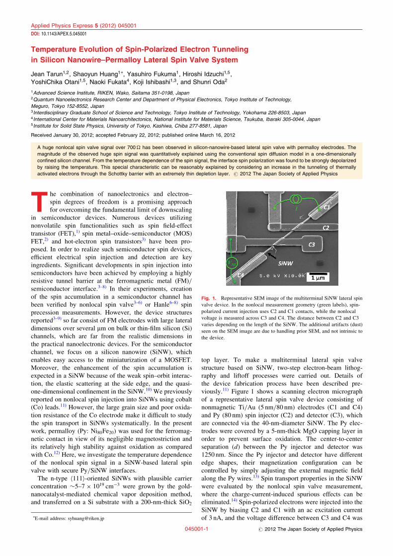
top layer. To make a multiterminal lateral spin valvestructure based on SiNW, two-step electron-beam lithog-raphy and liftoff processes were carried out. Details ofthe device fabrication process have been described pre-viously.11) Figure 1 shows a scanning electron micrographof a representative lateral spin valve device consisting ofnonmagnetic Ti/Au (5 nm/80 nm) electrodes (C1 and C4)and Py (80 nm) spin injector (C2) and detector (C3), whichare connected via the 40-nm-diameter SiNW. The Py elec-trodes were covered by a 5-nm-thick MgO capping layer inorder to prevent surface oxidation. The center-to-centerseparation (d) between the Py injector and detector was1250 nm. Since the Py injector and detector have differentedge shapes, their magnetization configuration can becontrolled by simply adjusting the external magnetic fieldalong the Py wires.13) Spin transport properties in the SiNWwere evaluated by the nonlocal spin valve measurement,where the charge-current-induced spurious effects can beeliminated.14) Spin-polarized electrons were injected into theSiNW by biasing C2 and C1 with an ac excitation currentof 3 nA, and the voltage difference between C3 and C4 was
Fig. 1. Representative SEM image of the multiterminal SiNW lateral spin
valve device. In the nonlocal measurement geometry (green labels), spin-
polarized current injection uses C2 and C1 contacts, while the nonlocal
voltage is measured across C3 and C4. The distance between C2 and C3
varies depending on the length of the SiNW. The additional artifacts (dust)
seen on the SEM image are due to handling prior SEM, and not intrinsic to
the device.
�E-mail address: [email protected]
Applied Physics Express 5 (2012) 045001
045001-1 # 2012 The Japan Society of Applied Physics
DOI: 10.1143/APEX.5.045001
measured via the ac lock-in technique at a frequency of17Hz. The in-plane magnetic field was swept from �50 to+50mT and vice versa.
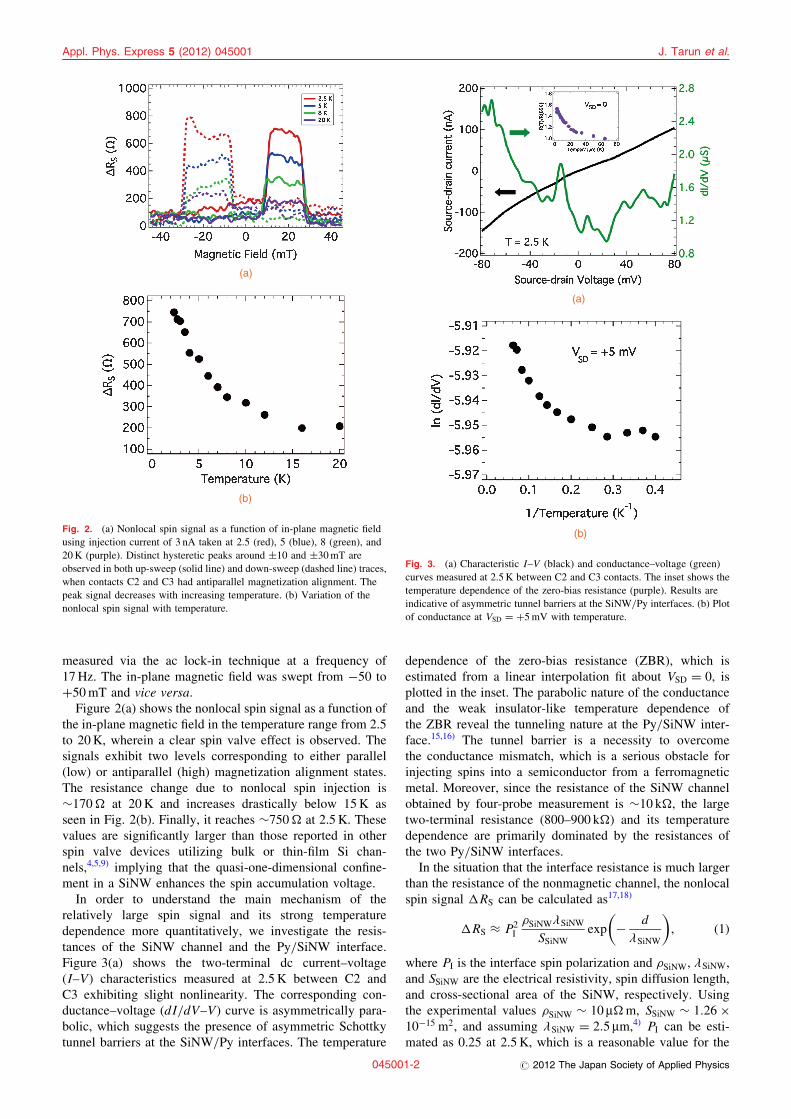
Figure 2(a) shows the nonlocal spin signal as a function ofthe in-plane magnetic field in the temperature range from 2.5to 20K, wherein a clear spin valve effect is observed. Thesignals exhibit two levels corresponding to either parallel(low) or antiparallel (high) magnetization alignment states.The resistance change due to nonlocal spin injection is�170� at 20K and increases drastically below 15K asseen in Fig. 2(b). Finally, it reaches �750� at 2.5K. Thesevalues are significantly larger than those reported in otherspin valve devices utilizing bulk or thin-film Si chan-nels,4,5,9) implying that the quasi-one-dimensional confine-ment in a SiNW enhances the spin accumulation voltage.
In order to understand the main mechanism of therelatively large spin signal and its strong temperaturedependence more quantitatively, we investigate the resis-tances of the SiNW channel and the Py/SiNW interface.Figure 3(a) shows the two-terminal dc current–voltage(I–V ) characteristics measured at 2.5 K between C2 andC3 exhibiting slight nonlinearity. The corresponding con-ductance–voltage (dI=dV–V ) curve is asymmetrically para-bolic, which suggests the presence of asymmetric Schottkytunnel barriers at the SiNW/Py interfaces. The temperature
dependence of the zero-bias resistance (ZBR), which isestimated from a linear interpolation fit about VSD ¼ 0, isplotted in the inset. The parabolic nature of the conductanceand the weak insulator-like temperature dependence ofthe ZBR reveal the tunneling nature at the Py/SiNW inter-face.15,16) The tunnel barrier is a necessity to overcomethe conductance mismatch, which is a serious obstacle forinjecting spins into a semiconductor from a ferromagneticmetal. Moreover, since the resistance of the SiNW channelobtained by four-probe measurement is �10 k�, the largetwo-terminal resistance (800–900 k�) and its temperaturedependence are primarily dominated by the resistances ofthe two Py/SiNW interfaces.
In the situation that the interface resistance is much largerthan the resistance of the nonmagnetic channel, the nonlocalspin signal �RS can be calculated as17,18)
�RS � P2I
�SiNW�SiNW
SSiNWexp � d
�SiNW
� �; ð1Þ
where PI is the interface spin polarization and �SiNW, �SiNW,and SSiNW are the electrical resistivity, spin diffusion length,and cross-sectional area of the SiNW, respectively. Usingthe experimental values �SiNW � 10 ��m, SSiNW � 1:26�10�15 m2, and assuming �SiNW ¼ 2:5 �m,4) PI can be esti-mated as 0.25 at 2.5K, which is a reasonable value for the
(a)
(b)
Fig. 2. (a) Nonlocal spin signal as a function of in-plane magnetic field
using injection current of 3 nA taken at 2.5 (red), 5 (blue), 8 (green), and
20K (purple). Distinct hysteretic peaks around �10 and �30mT are
observed in both up-sweep (solid line) and down-sweep (dashed line) traces,
when contacts C2 and C3 had antiparallel magnetization alignment. The
peak signal decreases with increasing temperature. (b) Variation of the
nonlocal spin signal with temperature.
(a)
(b)
Fig. 3. (a) Characteristic I–V (black) and conductance–voltage (green)
curves measured at 2.5K between C2 and C3 contacts. The inset shows the
temperature dependence of the zero-bias resistance (purple). Results are
indicative of asymmetric tunnel barriers at the SiNW/Py interfaces. (b) Plot
of conductance at VSD ¼ þ5mV with temperature.
J. Tarun et al.Appl. Phys. Express 5 (2012) 045001
045001-2 # 2012 The Japan Society of Applied Physics
Py electrode. This implies that the SiNW has comparablespin diffusion length as that of thin Si films even in thenanometer-sized cross section. This could be attributedto the elastic scattering events, which do not flip spins, atthe side edge of the SiNW.19) The SiNW therefore hasthe advantage over most nonmagnetic systems, which areknown to exhibit reduction in spin diffusion length withdecreasing cross-sectional area.20,21)
The nonlocal spin signal given by eq. (1) depends on threephysical parameters, �SiNW, �SiNW, and PI. As mentionedabove, the electrical resistivity of the SiNW, �SiNW, isalmost constant from 2.5 to 20K. This is because the freezeout effect can be negligible in highly doped degeneratedsemiconductors. We also expected that the spin diffusionlength of the SiNW, �SiNW, in this temperature range doesnot change significantly because phonon scattering eventsare suppressed. Therefore, the observed temperature changeof the spin signal is mainly caused by the change of theinterface spin polarization PI.
To elucidate the temperature dependence of the interfacespin polarization, we consider the influence of the thermalactivation during the tunneling process through the Py/SiNW Schottky barrier. Figure 3(b) shows the conductanceat VSD ¼ þ5mV (dI=dV jVSD¼þ5mV) as a function of tem-perature. The conductance becomes almost constant below4K, while it characteristically increases at higher tempera-tures. Assuming the activation behavior at the Py/SiNWinterface, the two-terminal conductance can be expressed as
dI
dV
����VSD¼þ5mV
ðT Þ ¼ G0 exp � Ea
kBT
� �; ð2Þ
where kB is the Boltzmann constant, G0 is a preexponentialfactor, and Ea is the activation energy. Fitting of theexperimental results yielded approximate values of 2.6mSand 0.5meV for G0 and Ea, respectively. The value of0.5meV is much smaller than the estimated Schottky barrierheight of �0:9 eV for the SiNW/Py contact.22,23) This maybe because the high donor concentration produces theextremely thin depletion layer width (5–10 nm). In such aSchottky barrier, the tunneling probability strongly dependson the energy level of the electron. That is, electrons athigher energy states have higher tunneling probability. Thismeans that the thermally activated electrons have highertunneling probability. Since the spin polarization of thethermally activated electrons is expected to be smallerthan that of the nonactivated electrons, the reduction of thenonlocal spin signal at higher temperatures can be explainedby the increase of the thermally activated electrons. Thus,the significant enhancement of the nonlocal spin signalbelow 10K can be understood by the suppression of thethermally activated electron tunneling events. This impliesthat the Schottky barrier in a highly doped semiconductor/
ferromagnetic metal interface is a crucial issue for theefficient spin injection at high temperatures.
In summary, nonlocal spin injection experimentswere carried out using a silicon nanowire-based lateral spinvalve with permalloy contacts. Because of the relativelysmall cross section of the SiNW, the obtained spin signalwas much larger than the values previously reportedin the devices composed of Si substrates and films. However,the spin signal was found strongly reduced by raisingthe temperature due to the depolarization of the tunnelingelectrons induced by the thermal activation. The suppres-sion of the tunneling of the thermally activated electronsmay be the key for the efficient spin injection at hightemperatures.
Acknowledgment We thank Professor Takashi Kimura of Kyushu
University for the fruitful discussions and careful reading of the manuscript.
1) S. Datta and B. Das: Appl. Phys. Lett. 56 (1990) 665.
2) S. Sugahara and M. Tanaka: Appl. Phys. Lett. 84 (2004) 2307.
3) I. Appelbaum, B. Huang, and D. J. Monsma: Nature (London) 447 (2007)
295.
4) T. Sasaki, T. Oikawa, T. Suzuki, M. Shiraishi, Y. Suzuki, and K. Noguchi:
Appl. Phys. Lett. 96 (2010) 122101.
5) O. M. J. van’t Erve, C. Awo-Affouda, A. T. Hanbiki, C. H. Li, P. E.
Thompson, and B. T. Jonker: IEEE Trans. Electron Devices 56 (2009)
2343.
6) B. T. Jonker, G. Kioseoglou, A. T. Hanbicki, C. H. Li, and P. E.
Thompson: Nat. Phys. 3 (2007) 542.
7) S. P. Dash, S. Sharma, R. S. Patel, M. P. Jong, and R. Jansen: Nature
(London) 462 (2009) 491.
8) R. Jansen, B. C. Min, S. P. Dash, S. Sharma, G. Kioseoglou, A. T.
Hanbicki, O. M. J. van’t Erve, P. E. Thompson, and B. T. Jonker: Phys.
Rev. B 82 (2010) 241305(R).
9) Y. Ando, K. Kasahara, K. Yamane, K. Hamaya, K. Sawano, T. Kimura,
and M. Miyao: Appl. Phys. Express 3 (2010) 093001.
10) I. Zutic, J. Fabian, and S. Das Sarma: Rev. Mod. Phys. 76 (2004) 323.
11) J. Tarun, S.-Y. Huang, Y. Fukuma, H. Idzuchi, Y. Otani, N. Fukata, K.
Ishibashi, and S. Oda: J. Appl. Phys. 109 (2011) 07C508.
12) D. Y. Petrovykh, K. N. Altmann, H. Hochst, M. Laubscher, S. Maat, G. J.
Mankey, and F. J. Himpsel: Appl. Phys. Lett. 73 (1988) 3459.
13) W. Y. Lee, Y. B. Xu, C. A. F. Vaz, A. Hirohata, H. T. Leung, C. C. Yao,
B.-C. Choi, J. A. C. Bland, F. Rousseaux, E. Cambril, and H. Launois:
IEEE Trans. Magn. 35 (1999) 3883.
14) S. Takahashi and S. Maekawa: Phys. Rev. B 67 (2003) 052409.
15) B. J. Johnsson- �Akermann, R. Escudero, C. Leighton, S. Kim, I. K.
Schuller, and D. A. Rabson: Appl. Phys. Lett. 77 (2000) 1870.
16) J. M. Rowell: in Tunneling Phenomena in Solids, ed. E. Burnstein and S.
Lundqvist (Plenum, New York, 1969).
17) M. Johnson and R. H. Silsbee: Phys. Rev. Lett. 55 (1985) 1790.
18) F. J. Jedema, H. B. Heersche, A. T. Filip, J. J. A. Baselmans, and B. J.
van Wees: Nature (London) 416 (2002) 713.
19) E. Ramayya, D. Vasileska, S. M. Goodnick, and I. Knezevic: J. Phys.:
Conf. Ser. 38 (2006) 126.
20) T. Kimura, T. Sato, and Y. Otani: Phys. Rev. Lett. 100 (2008) 066602.
21) A. Vogel, J. Wulfhorst, and G. Meier: Appl. Phys. Lett. 94 (2009) 122510.
22) B.-C. Min: Dr. Thesis, University of Twente, The Netherlands (2007).
23) S. M. Sze: Physics of Semiconductor Devices (Wiley, New York, 1981)
2nd ed., Chap. 3.
J. Tarun et al.Appl. Phys. Express 5 (2012) 045001
045001-3 # 2012 The Japan Society of Applied Physics
Related Documents