Jordi Mateu Research Associate April - 2005 Telecommunications Technological Center of Catalonia (CTTC)

Welcome message from author
This document is posted to help you gain knowledge. Please leave a comment to let me know what you think about it! Share it to your friends and learn new things together.
Transcript

Jordi MateuResearch Associate
April - 2005
TelecommunicationsTechnological Center of Catalonia
(CTTC)

2 / 14
WPR3: Design, Modeling and Characterization of RF and MicrowaveDevices and Subsystems ( 0.4 MM )
NEWCOMNEWCOM
Nonlinear ModelingDistributed nonlinear effects
• “Nonlinear Distortion in a 8-pole Quasi-elliptic bandpass HTS filter forCDMA systems” J Mateu, C. Collado, O. Menendez, J.M. O’Callaghan. IEEE Trans.On Applied Superconductivity To be published in June 2005.
Antenna designsUltra-wideBand Antennas
• “Bow-tie shaped UWB planar antenna using a double-sided impedancematching network” P. Miskovsky, J. Mateu, A. Mollfulleda, J. Romeu. Submittedto IEEE International Conference UltraWideBand, Zurich, October 2005.

3 / 14
Nonlinear Nonlinear ModelingModeling
Antenna
Cable
RF front-end, Trec
Bandpassfilter
LNA
NONLINEARITIES
might degrade the system performance
• The performance of wireless base-station can be considerably enhancedby incorporating LNAs with HTS filters.
Broadbandmodulated signals
strong
out-of band
weak in-band
??•Spectral regrowth•Intermixing products
Microwave Nonlinearities in Superconductors
Nonlinear System Performance
• Filter Selectivity
• Nonlinear effects
• Broadband signals

4 / 14
Nonlinear Nonlinear ModelingModeling ∆L(i), ∆R(i)
• The equivalent circuit of HTSline resonators is wellestablished.
Ro dz Lo dz ∆R(i)dz ∆L(i)dz
C dz G dz v v+dv
- dv + + d vl - + dvnl - i i+di
+
-
+
-
This is used to build an equivalent circuit to makerealistic predictions of nonlinear effects in a HTS filter.
Numerical Techniques
• Harmonic Balance (HB) has been proven usefulto simulate this equivalent circuit.
• HB is sufficiently fast to adjust circuit elementsto match simulations to IMD measurements.
dz
5 / 14
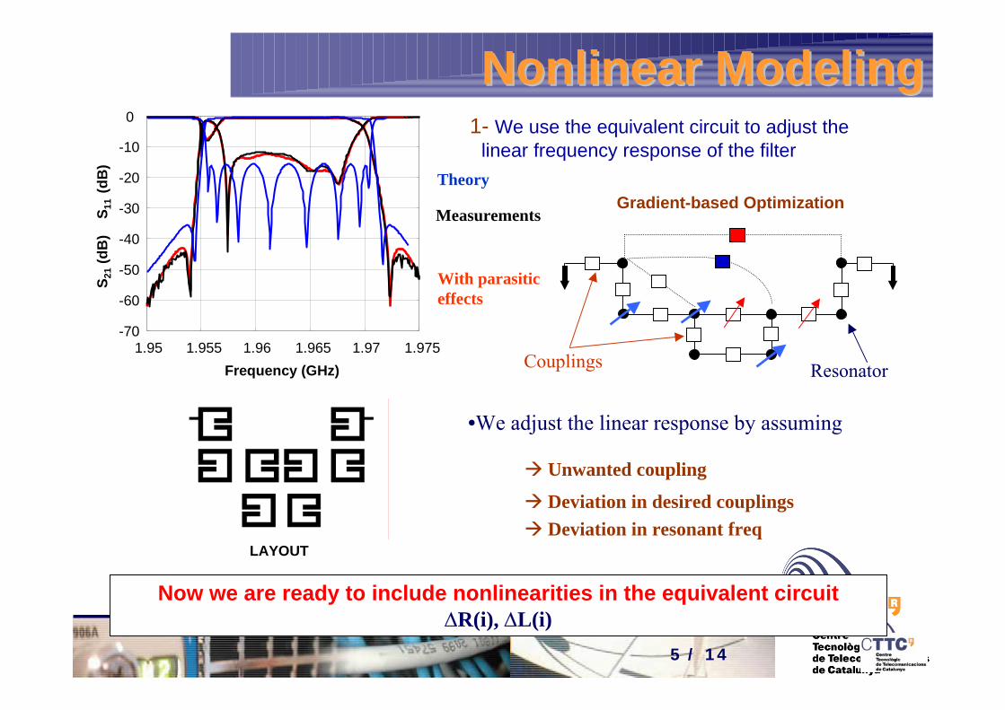
Nonlinear Nonlinear ModelingModeling
Measurements
1.95 1.955 1.96 1.965 1.97 1.975-70
-60
-50
-40
-30
-20
-10
0
Frequency (GHz)
S 21 (
dB)
S11
(dB
)
With parasiticeffects
Theory
•We adjust the linear response by assuming
Gradient-based Optimization
1- We use the equivalent circuit to adjust thelinear frequency response of the filter
ResonatorCouplings
LAYOUT
Unwanted coupling
Deviation in resonant freq
Now we are ready to include nonlinearities in the equivalent circuit∆R(i), ∆L(i)
Deviation in desired couplings

6 / 14
Nonlinear Nonlinear ModelingModelingBasic resonant structure
Equivalent circuit
The most important contribution inthe nonlinear effects takes placewhere the current density is largest
We model the whole filter as a halfwave straightHTS Nonlinear lines coupled each other
Narrow band filter Weak coupling between resonatorsWe assume the profile of the currentdistribution in the resonators is almost thesame that would be in an isolated structure
[3EG02]
7 / 14
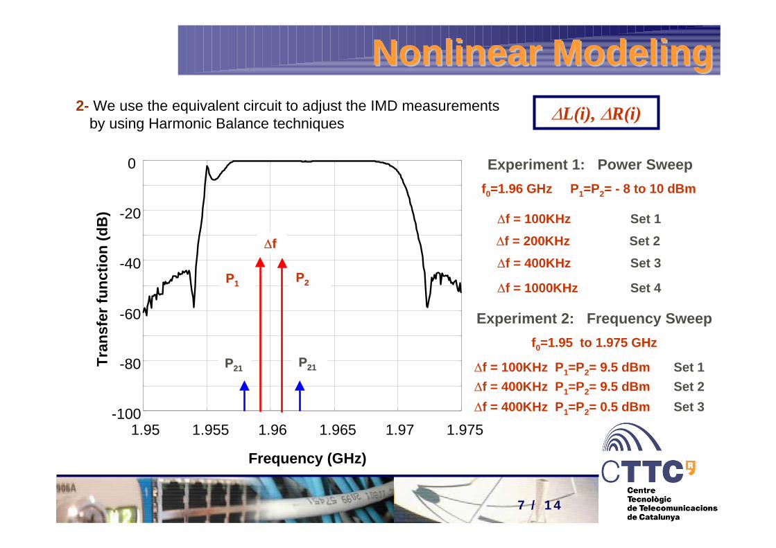
Nonlinear Nonlinear ModelingModeling2- We use the equivalent circuit to adjust the IMD measurements
by using Harmonic Balance techniques
1.95 1.955 1.96 1.965 1.97 1.975-100
-80
-60
-40
-20
0
Frequency (GHz)
Tran
sfer
func
tion
(dB
)
∆∆f f
PP22PP11
PP2121PP2121
Experiment 1: Power Sweepf0=1.96 GHz P1=P2= - 8 to 10 dBm
∆f = 100KHz Set 1∆f = 200KHz Set 2∆f = 400KHz Set 3
∆f = 1000KHz Set 4
Experiment 2: Frequency Sweepf0=1.95 to 1.975 GHz
∆f = 100KHz P1=P2= 9.5 dBm Set 1∆f = 400KHz P1=P2= 9.5 dBm Set 2∆f = 400KHz P1=P2= 0.5 dBm Set 3
∆L(i), ∆R(i)
8 / 14
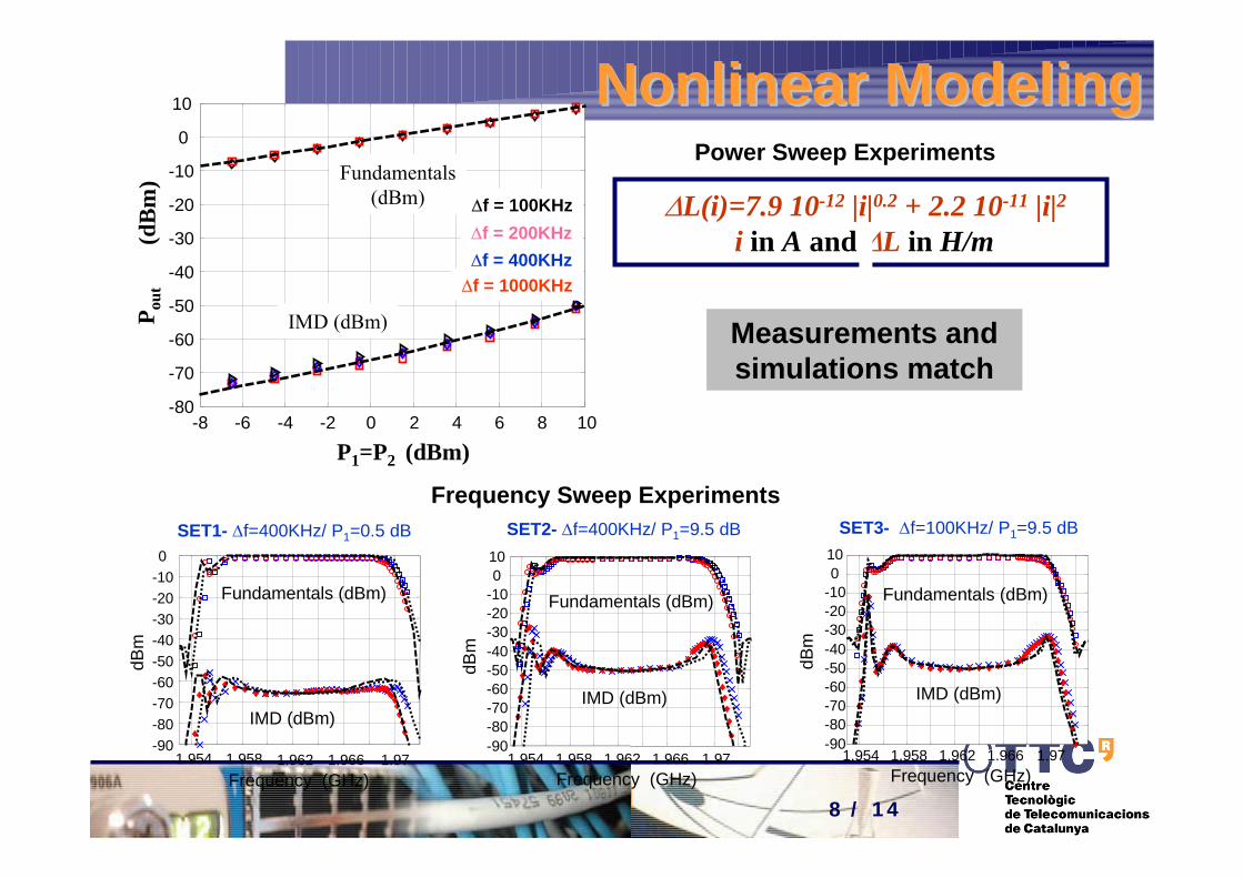
Nonlinear Nonlinear ModelingModeling
Frequency Sweep Experiments
1.954 1.958 1.962 1.966 1.97-90-80-70-60-50-40-30-20-100
Frequency (GHz)
IMD (dBm)
Fundamentals (dBm)
dBm
1.954 1.958 1.962 1.966 1.97-90-80-70-60-50-40-30-20-10010
Frequency (GHz)
IMD (dBm)
Fundamentals (dBm)
dBm
1.954 1.958 1.962 1.966 1.97-90-80-70-60-50-40-30-20-10010
Frequency (GHz)
IMD (dBm)
Fundamentals (dBm)
dBm
SET1- ∆f=400KHz/ P1=0.5 dB SET2- ∆f=400KHz/ P1=9.5 dB SET3- ∆f=100KHz/ P1=9.5 dB
Power Sweep Experiments
-8 -6 -4 -2 0 2 4 6 8 10-80
-70
-60
-50
-40
-30
-20
-10
0
10
Fundamentals(dBm)
IMD (dBm)
P1=P2 (dBm)
P out
(d
Bm
)
∆f = 100KHz∆f = 200KHz∆f = 400KHz∆f = 1000KHz
∆L(i)=7.9 10-12 |i|0.2 + 2.2 10-11 |i|2 i in A and ∆L in H/m
Measurements andsimulations match

9 / 14
Nonlinear Nonlinear ModelingModelingCo-sitting of TDD and FDD UMTS base-stations
TDD FDD (Uplink)T1 T2 T3 T4 F1 F2 F3 F4
A B C
TDD-FDD
1900 MHz 1920 MHz 1980 MHz
Co-sitting TDD-FDDCo-sitting TDD-FDD
• UMTS- FDD base station filtersubject to interference of anearby TDD emitter.
1.945 1.95 1.955 1.96 1.965 1.97 1.975-220
-200-180-160-140-120-100-80-60-40-20
0
• Nonlinearities cause spectralregrowth and might block thebase station.
-60
-40
-20
0
dBm
/Hz
dB
Frequency (GHz)
10 / 14
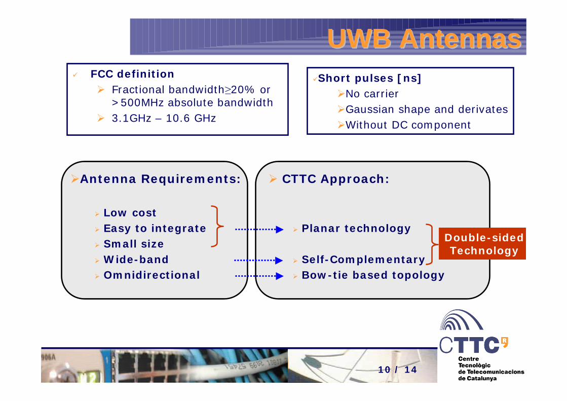
UWB AntennasUWB Antennas
Antenna Requirements:
Low cost Easy to integrate Small size Wide-band Omnidirectional
CTTC Approach:
Planar technology
Self-Complementary Bow-tie based topology
Double-sidedTechnology
FCC definitionFractional bandwidth≥20% or>500MHz absolute bandwidth3.1GHz – 10.6 GHz
Short pulses [ns]No carrierGaussian shape and derivatesWithout DC component

11 / 14
UWB AntennasUWB Antennas
Antenna Subsystem
Radiating UnitMatching/FilteringNetwork
MatchingTechnologies
Double-SidedBow-tie Shaped
Double-SidedMatching impedanceFiltering
Double-SidedTo
Microstrip

12 / 14
UWB AntennasUWB AntennasBow-tie shaped antenna
-Bow-tie shaped antenna with acircle tangent to a 90 deg triangle
- feedline width optimized
Radiating Unit

13 / 14
UWB AntennasUWB AntennasAntenna, matching network and technology transformer

14 / 14
UWB AntennasUWB Antennas
0 1 2 3 4 5 6 7 8 9 10 11 -30
-25
-20
-15
-10
-5
0
frequency [GHz]
S11
[dB
] simulatedmeasured
Gai
n (d
B)
Frequency (GHz) 3 4 5 6 7 8 9 10 11
-10
-8
-6
-4
-2
0
2
4
62 bow-tiesbow-tie and Ridge
-Antenna gain has been measuredfirst using the same antenna as aprobe, then using a ridge antenna asprobe
- Major gain oscillation is observedprobably due to reflections from amicrostrip ground plane
-100 -80 -60 -40 -20 0 20 40 60 80 100-45
-40
-35
-30
-25
-20
-15
-10
-5
0
5
copolar polarization
angle [deg]
3 GHz5 GHz7 GHz9 GHz
- radiation pattern at low frequencies presentsundesired variations probably due to a GNDplane of a microstrip section
- at high frequencies the sidelobes becamemore important
- in general the radiation pattern is not stablewithin whole FCC-UWB frequency range
Related Documents