Technical Manual MAG;PAK SERIAL MAGNETIC TAPE SYSTEM MODELS 9446/9448 SDS 900647B October 1965 Pri ce: $8. 00 This publication supersedes the following publications: SD S 900647 A dated January 1965 SDS 900829A dated 1 March 1965 SDS 900830A dated 1 March 1965 SD S 900842A dated March 1965 SCIENTIFIC DATA SYSTEMS. 1649 Seventeenth Street • Santa Monica, Calif. • (213) 871-0960 © 1965, Sci enti fi c Data Systems, Inc.

Welcome message from author
This document is posted to help you gain knowledge. Please leave a comment to let me know what you think about it! Share it to your friends and learn new things together.
Transcript

Technical Manual MAG;PAK
SERIAL MAGNETIC TAPE SYSTEM MODELS 9446/9448
SDS 900647B
October 1965
Pri ce: $8. 00
This publication supersedes the following publications:
SD S 900647 A dated January 1965 SDS 900829A dated 1 March 1965 SDS 900830A dated 1 March 1965 SD S 900842A dated March 1965
"I··I~ SCIENTIFIC DATA SYSTEMS. 1649 Seventeenth Street • Santa Monica, Calif. • (213) 871-0960
© 1965, Sci enti fi c Data Systems, Inc.
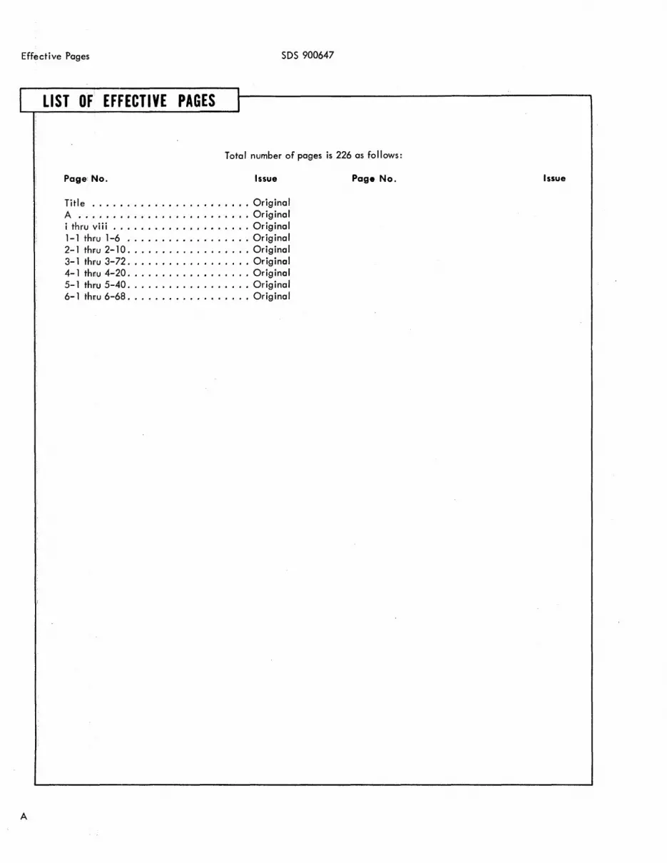
Effective Pages SDS 900647
I LIST OF EFFECTIVE PAGES I
r
Total number of pages is 226 as follows:
A
Page No. Issue
Title ..•.•..••..•...•.•.•... Original A ..........•........•..•.. Original i thru viii .....•.....•..•..... Original 1-1 thru 1-6 .................. Original 2-1 thru 2-10 .................. Original 3-1 thru 3-72 .................. Original 4-1 thru 4-20 .................. Original 5-1 thru 5-40 .................. Original 6-1 thru 6-68 .................. Original
Page No. Issue

SDS 900647 Contents
TABLE OF CONTENTS
Section Title Paqe
GENERAL DESCRIPTION 1 1
1- 1 Introduction. . . • • • • • . • • • • • • • • • • • • • • • • • • • • • • • • • • • • • • • • • • • • • • • • • • • • •• 1 Ccc 1 1-2 Scope of Manual •.•.••••••••.••••.•.•••••••...•..••..•..•.•.••.•• 1··,1 1-4 Purpose of Equipment. • • • • • • . • • • • • • • • • • • • • • • • • • • • • • . • . • • • • • . • • • • • • •• 1 1 1-6 Typical Applications. • • • • • • • • • • • • • . . • • . • • • • . • • • . . . . • . . • . • • • • • • • • . •. 1 1 1-8 Physical Description .•••.••.•••.••••••.••. ~ . • • . . . • • • . • • • . • • • • . • • . • • . •. 1 ·,1 1- 10 Model 9446 Tape Transport Unit . • • . • • • • • • . • • • . • • . . • . . . • . . . • . . . • • • . • . • •. 11 1-13 Model 9448 Tape Control Unit •...•••.. 0 • 0 ••• 0 0 0 0 0 •••••• 0 0 • 0 0 0 0 •• 0 0 0 •• 0 1- 1 1-15 Model 9401 Tape Cartridge •••• 0 •• 0 • 0 ••• 0 •• 0 •• 0 0 0 0 0 0 •••••••••• 0 •• 0 0 • •• 1 1 1-17 Specifications ..•... 0 ••• 0 •••••• 0 • 0 0 •••• 0 0 • 0 • 0 • 0 •••••••••• 0 •••••• 0 • 0 0 1 1 1-19 Functional Description •.. 0 • 0 0 0 • 0 ••• 0 • 0 • 0 • 0 ••••• 0 • 0 0 0 0 0 0 • 0 ••••••• 0 •••• 0 0 1 5
II OPERATION AND PROGRAMMING .. 0 0 •• 0 ••••••••••• 0 0 0 •• 0 0 0 • 0 •• 0 0 0 • 0 •••• 0 0 0 0 0 0 0 2-1
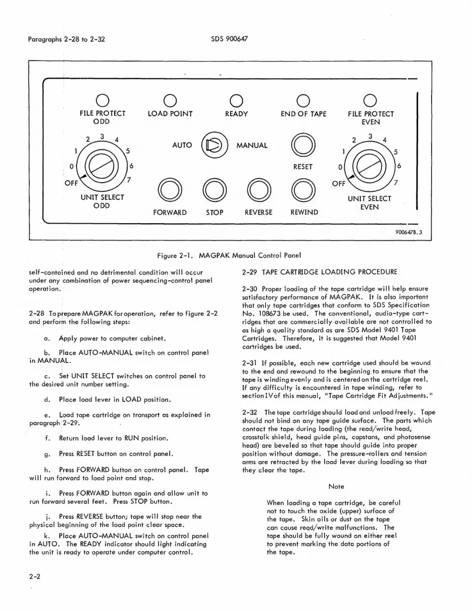
2- 1 Operating Instructions . 0 • 0 •• 0 ••• 0 0 0 •• 0 0 0 0 0 •• 0 • 0 • 0 0 •• 0 0 0 0 • 0 •• 0 0 • 0 0 •• 0 •• 0 2- 1 2-2 Controls and Indicators. 0 •• 0 0 0 0 • 0 • 0 ••• 0 • 0 •• 0 ••• 0 ••• 0 ••••• 0 •••••• 0 • 0 0 0 2- 1 2-4 Auto-Manual Switch ..... 0 •• 0 ••••••• 0 ••••••• 0 0 0 •• 0 0 ••••••• 0 •• 0 •• 2," 1 2-6 Un it Select Switches . 0 • 0 • 0 0 •••• 0 0 0 • 0 0 0 •• 0 0 0 0 0 •• 0 0 0 •••••• 0 • 0 0 0 • •• 2- 1 2-8 Forward Pushbutton .... 0 •• 0 •• 0 • 0 •• 0 0 • 0 • 0 0 ••• 0 0 ••••••••• 0 • 0 ••••• 0 2- 1 2-10 Reverse PLJshbutton .•. ' ..•. 0 ••••••• 0 • 0 ••• 0 •• 0 0 •••• 0 ••••••••• 0 0 • 0 o. 2- 1 2-12 Rewind Pushbutton. 0 0 ••••• 0 0 ••• 0 0 • 0 •• 0 • 0 • 0 0 • 0 0 0 • 0 •• 0 •• 0 •••••• 0 0 0 2- 1 2-14 Stop Pushbutton . 0 •• 0 • 0 0 •• 0 •• 0 •• 0 • 0 •• 0 ••• 0 0 0 •• 0 •••••••••••••• o. 2- I 2- 16 Reset Pushbutton .. 0 • 0 0 •••• 0 ••• 0 • 0 0 ••• 0 • 0 •• 0 0 0 •••• 0 0 0 • 0 0 ••• 0 0 0 •• 2- I 2- 18 Fi Ie Protect Indicators . 0 ••• 0 ••• 0 ••• 0 • 0 0 • 0 •• 0 0 0 •• 0 0 0 •••• 0 • 0 • 0 • 0 0 •• 2- 1 2-20 Load Point Indicator ....... 0 ••••• 0 ••• 0 •• 0 0 • 0 ••••• 0 •••• 0 • 0 ••••••• 0 2- I 2-22 End of Tape Indicator .. 0 0 •• 0 0 0 ••••••• 0 • 0 • 0 ••• 0 •• 0 0 ••••• 0 • 0 0 0 • 0 • •• 2- I 2-24 Ready Indicator . 0 ••• 0 0 0 • 0 •• 0 •• 0 • 0 0 0 0 0 • 0 • 0 0 • 0 •• 0 •• 0 •••• 0 •••• 0 • 0 2- CI
2-26 Turn On/Turn Off Procedures 0 0 0 •• 0 •• 0 0 •••• 0 ••• 0 •• 0 • 0 0 •• 0 • 0 •••••••• 0 • •• 2-1 2-29 Tape Cartridge Loading Procedure ........ 0 • 0 • 0 • 0 • 0 0 • 0 0 •••• 0 •• 0 •• 0 0 0 0 0 • o. 2-2 2-34 Tape Cartridge Unloading Procedure .. 0 • 0 0 • 0 ••••• 0 •• 0 •••• 0 ••• 0 ••• 0 0 •• 0 0 • 0 2-4 2-37 Placement of File Protect (Write) Plugs . 0 •••• 0 0 • 0 ••••• 0 ••••• 0 • 0 0 0 0 •••• 0 • 0 0 2-1 2-39 Placement of Load-Point Clear Space and End-Of- Tape Markers 0 •••• 0 •• 0 ••••• 0 • • •• 2-4 2-41 Programm ing o .... 0 •• 0 •••• 0 0 0 • 0 0 • 0 •• 0 0 0 0 0 0 0 • 0 0 0 •• 0 •••••• 0 0 ••• 0 0 ••• 0 0 2-4 2-42 Introduction ....... 0 •• 0 •••••• 0 0 0 0 ••••• 0 0 • 0 ••• 0 ••••• 0 •••••••••••• 0 2-4 2-44 Without-Leader EOM Instructions. 0 0 •••• 0 • 0 0 •• 0 0 0 ••••••••••••• 0 • • • • •• 2-1 2-46 Four-Character Mode . 0 • co 0 0 0 0 ••••• 0 0 • 0 0 ••• 0 0 0 0 • 0 •••••• 0 ••• 0 0 • 0 0 0 2-4 2-48 Timing Considerations ... 0 ••• 0 •••••• 0 • 0 ••• 0 0 ••••••••••••••••••• o. 2-4 2-50 Longitudinal Check Character .......... 0 • 0 0 ••• 0 •••••• 0 •• 0 ••••• 0 •• o. 2· 5 2-52 Buffer Ready Indication .... 0 0 •••••••• 0 •• 0 •••• 0 ••• 0 ••• 0 •••• 0 • 0 • • •• 2-5 2-55 Reading Beyond the Last Write . 0 0 • 0 • 0 0 0 •• 0 ••• 0 0 •••••• 0 0 ••••••• 0 • • •• 2- 5 2-57 Backspace or Rewind After a Write . 0 0 ••• 0 ••••••••••••••• 0 • • • • • • • • • • •• 2-5 2-59 Tape Transport Unit Status Signals. . . . . . . . . . . . . . . . . . . . . . . . . . . . . . . . . . . . . .. 2-5 2-61 Tape-Unit-Ready Test . . . . . . . . . . . . . . . . . . . . . . . . . . . . . . . . . . . . . . . . . .. 2-5 2-63 Fi le- Protect Test ..... 0 0 •••• 0 • 0 0 0 0 0 ••••• 0 •••••••••• 0 • • • • • • • • • • •• 2-5 2-65 Beginning·-of-cTape Test ....... 0 • • • • • • • • • • • • • • • • • • • • • • • • • • • • • • • • •• 2-6 2-67 End-of- Tape Test ......... 0 •••••••• 0 • 0 0 •••••• 0 •• 0 0 ••• 0 • 0 • • • • • • •• 2-6 2-69 Density Tests. 0 • 0 •••••• 0 0 •••••••• 0 ••••••••••••••• 0 • • • • • • • • • • •• 2-6 2-71 End-of-File Test ................. 0 •••• 0 •••• 0 0 • 0 • 0 •••••••• 0 • • •• 2-6 2-73 Gap Test. . . . . . . 0 • • • • • • • • • • • • • •• 0 0 0 •• 0 0 ••• 0 • • • • • • • • • 0 • • • • • • •• 2-6 2-76 Skip If Not MAGPAK .. 0 •••••••••••••••• 0 •• 0 •• 0 0 • 0 •••••••••••••• 0 2-6

Contents
Section
III
ii
2-78 2-79 2-82 2-87 2-89 2-91 2-93 2-95 2-96 2-98 2-101 2-103 2-104 2-106 2-108 2-110 2-112 2-113 2-115 2-117 2-119 2-122 2-124 2-126 2-128 2-129 2-131 2-133 2-135
TABLE OF CONTENTS (Cont.)
Title Page
Writing. . . . . . . . . . . . . . . . . . . . . . . . . . . . . . . • . . . . . . . . . . . . . . . . . . . . . . .. 2-6 Introduction ...........•..................................... 2-6 Write Errors. . . . . . . . . . . . . . . . . . . . . . • . . . . . . . . . . . . . . . . . . . . . . . . . .. 2-6 Writing From the Load Point Marker . . . . . . . . . . . . . . . . . . . . . . . . . . . . . . . . .. 2-7 Writing Near the End of Tape ... . . . . . . . . . . . . . . . . . . . . . . . . . . . . . . . . . .. 2-7 End-of-File Definition. . . . . . . . . . . . . . . . . . . . . . . . . . . . . . . . . . . . . . . . . .. 2-7 Writing the Tape Mark. . . . . . . . . . . . . . . . . . . . . . . . . . . . . . . . . . . . . . . . . .. 2-7
Erasing. . . . . . . . . . . . . . . . . . . . . . . . . . . . . . . . . . . . . . . . . . . . . . . . . . . . . . .. 2-7 Introduction ................................................. 2-7 Erasing a Record After a Write Error ............... . . . . . . . . . . . . . . . . . . . 2-7 Erasing a Given Length of Tape. . . . . . . . . . . . . . . . . . . . . . . . . . . . . . . . . . . .. 2-8
Reading. . . . . . . . . . . . . . . . . . . . . . . . . . . . . . . . . . . . . . . . . . . . . . . . . . . . . . .. 2-8 Introduction ................................................. 2-8 Long Records . . . . . . . . . . . . . . . . . . . . . . . . . . . . . . . . . . . . . . . . . . . . . . . .. 2-8 Reading an End-of-File. . . . . . . . . . . . . . . . . . . . . . . . . . . . . . . . . . . . . . . . . .. 2-8 Reading an the End of the Tape .......... . . . . . . . . . . . . . . . . . . . . . . . . . .. 2-8
Scann ing and Search ing . . . . . . . . . . . . . . . . . . . . . . . . . . . . . . . . . . . . . . . . . . . .. 2-8 Introduction ................................................. 2-8 Continued Scan ............................................... 2-8 Reverse Search ............................................... 2-8 Forward Search. . • . . . . . . . • . . . . . . . . . . • . . . . . . . . . . . . . . • • . • . • . . . . . . 2-9 Scann ing an End-of-Fi Ie Record. . . . . . . . . . • . . . • • . . . • . • . . . . . . • . • • • . • .. 2-9 Scanning Near the Beginning of Tape .......•..•••........•....•..••.. 2-9 Scanning Near the End of Tape ............••....•••..........•.•... 2-9
Spacing. . . . . . . . . • . . . • . . . • . . . . • . . • . . . . • . . • • . . . . . . . . . . . . . . • . . . . . . 2-9 Space Forward or Reverse, One Record. . . . . . . . • . • . . . . • . . . . . . . . . . . . . • . .. 2-9 Space More Than One Record. . . . . . . . . . . • . . . . . . . . . . . . . . . . . . . . • • • . . .. 2-9
Rewinding. . . . . . . . . . . . . . . . . . . . . . . . . . . . . . . . . . . . . . . . . . . . . . . . . . . . .. 2-9 Summary of Tape Operation Codes .. . . . . . . . . . . . . . . . . . . . . . . . . . . . . . . . . . . .. 2-9
THEORY OF OPERATION ................................................... . 3-1
3-1 3-1 3-1 3-2 3-3 3-3 3-3 3-3 3-3 3-3 3-3 3-4 3-4 3-8 3-8 3-8 3-8 3-9 3-9 3-9 3-9 3-9 3-9 3-9
3- 1 Introduction ...........•..................•....••.•..•..•........•. 3-3 MAGPAK Coding Sche;;e .............................................. . 3-8 Read Decoding Time Interva Is ..............••...•.......•.•.•..•...... 3-16 MAGPAK Record Format ..........•...•......••..•.•.•...••..•.•.•..... 3-24 Tape Transport Unit Electromechanical Description .•.•...•.•.•.•••••....•..••••. 3-26 Tape Drive System ........•.....•.....••.........•••..•••••..••..•. 3-27 Forward and Reverse ' ............•.....•...........•.•.......•.•. 3-29 Capstan Motor and Pulley Hub.. . ..................•............ 3-30 Drive Belt and Idler Pulley .................................... . 3-31 Capstans and Capstan Pull ies ....•............................... 3-32 Pressure Rollers and Solenoids .................................. . 3-34 Ree I Motor Brakes .......................... ............... . 3-35 Rewind ................................................. . 3-50 Tension Arm Lim it Switches .................................... . 3-52 File Protect Switches ........................................ . 3-54 Read Circuits ................................................... . 3-56 HX30 Gated Read Ampl ifier ................................... . 3-58 HX29 Data Ampl ifier ........................................ . 3-61 Filter ................................................. . 3-62 Differentiator ............................................. . 3-63 Linear Ampl ifier ........................................... . 3-64 Squaring Ampl ifier ......................................... . 3-65 Line Driver .............................................. . 3-66 Threshold Detector ......................................... .

Section
3-67 3-68 3-70 3-72 3-74 3-76 3-79 3-80 3-83 3-84 3-87 3-92 30-94 30-96 30-100 3,-102 3,-105 30-111 3,-115 3-118 3,-121 3-124 3-126 3·-128 3-130 3-133 3·-135 3·-137 3-141 3-143 3-148 3·-153 3-155 3·-157 3·-159 3-161 3·-163 3·-165 3·-167 3·-169 3·-171 3-172 3·-177 3·-178 3-181 3·-184 3-187 3--188 3-192 3--197 3--199 3--211 3--222 3--223 3--225 3--230
SDS 900647
TABLE OF CONTENTS (Cont.)
Title
Threshold Selector Tape Transport Unit Functional Description .....•.••.....••........•.......•.
Status/Select .........••.. " .•.•.•....••.....••..........•...... Motion Control .........•••••.•.•.•••....•..•.........•......... Data Transfer .......•......•.•.•...•.•......•..........•....... Typical Programmed Sequence ..•......•.•.•••••.•.••...........•....
Tape Transport Unit Logic Description ••.•.•.••••..•.•....•....•........••. Introduction ......••.•••.••.•••.••........••••..•..•....•..•.. Status/Select Logic ......•.••. " ••.•.••••.•.••.•......••..........
Unit Select Lines ....•..••••••••.•.•...•.....•....•.....•.•.. Ready ........•...•••.....••••.•.•...•.........•.•.....•.. End-of- Tape .......••••..•....••........................... Beg inn ing--of-Tape ........•..•..•.••...•.•....•.•...•.......... File Protect .....•.....•...•.•.••......••..........•........ Indicators ............•.•.•••..•••..•.••.••....••..........
Motion Control Logic .......••. , .. , ........• , •.......• , .••....... , Manual Control ...•...•............•.............•..........
Automatic Control .......•..•.•.•...••.............•.......... Data Transfer Logic .........•.....••....•.............•..........
Reading ......•......•......•.•..... , ..........•.......... Writing ....•......•.•.......•............................
Tape Control Unit Functional Description .......................•.......... Write Logic Section .........•........................••..........
Write Clock Generator ..•.•.................................... Write Synchronizer ......•....................................
Read Logic Section .........•......•....•.......•................ Read Signer! Standardizer ...................................... . Read Decoder. . . . . . . . . . • . . . . . . . . . . . . . . . . . . . . . . . . . . . . . . . . . . .. Read FI ip-Flop ........••.................................... Read Synchronizer .............•........•.....................
Harvey Register Section ....•.•....•...•.....•...... ' .............. . Control Logic Section ..•••••••••••••.•.•.•.••.••...•••.••••••.•••
Control Stote Counter ....•.....•...•.........•.•.............. External Clock Flip-Flop .........•.......•...•......•.....•.... Reverse Monitor Flip-Flop ......••••.•.••.••....•.•...•.•..••.... Erase Tape Flip-Flop .....•....•.. ' ....•..••..•...••••.•..••.... Enable ReCid Flip-Flop .. ' ..•...•..•.• , ....•.•....• , .• , ••.•..•... File Mark FI ip-Flop ....•...•.•.••.... ,., .......•.•.....•..... Continue FI ip-Flop ...••.......•.....••..•..•............... -Skip Remainder Flip-Flop ..........•.•.•.......•............•...
Tape Control Un it Logic Description ......••..••.•..•..•.•...••. , , ••...•.. Introduction ...•..........•.•.•• , • ' •.•••.....•.....•.•.•.•...... Write Logic Description ~ .....••...•.•...•...•.......•.............
Write Clock Generator Logic ........••..........•.•.•............ Write Synchron izer Logic ........••......•....•................ Write FI ip--Flop Logic ..........•....•............•............
Read Logic Discription ............•..•....•.....•..•.•............ Read Signa I Standardizer .....•.•.....•••.••...•..........•..... Read Decoder ....•......•.•..•••••.•...•...... •..•.•.••..•• Read FI ip-Flop ..............•.•.....................•.....•. Read Synchronizer .•.....••.....•.•••..•..•.......•..•.......
Harvey Register Logic Description .•..............•...•...•..•......•.. Control Logic Description .............•..............••...........•
Introduction ..................•...•......................•. Selection and Starting (CSO) .......••......................•..... Write or Erase Forward (CSO) ..............•......................
Contents
Page
3-9 3-9 3-9 3-9 3-9 3-9 3-10 3-10 3-13 3-13 3-13 3-13 3-13 3-14 3-14 3-14 3-14 3-15 3-15 3-15 3-16 3-16 3-16 3-16 3-16 3-16 3-19 3-19 3-19 3-19 3-19 3-20 3-20 3-22 3-22 3-22 3-22 3-22 3-22 3-22 3-23 3-23 3-23 3-23 3-24 3-25 3-25 3-26 3-29 3-29 3-34 3-35 3-35 3-35 3-36 3-36
iii
Contents
Section
IV
V
IV
iv
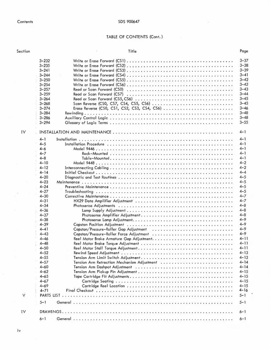
3-232 3-235 3-241 3-244 3-250 3-254 3-257 3-259 3-264 3-268 3-274 3-284 3-286 3-294
5D5900647
TABLE OF CONTENTS (Cont.)
Title
Write or Erase Forward (C51) ......•••••••..•..•.••...•...•.••••••• Write or Erase Forward (C52) ..•••....•..•..........•..........•... Write or Erase Forward (C53) ..................................... . Write or Erase Forward (C54) ...•..........•....................... Write or Erase Forward (C55) ..................................... . Write or Erase Forward (C56) .....................•............•... Read or Scan Forward (C50) ............•......................... Read or Scan Forward (C57) ..................................... . Read or Scan Forward (CS5, CS6) .................................. . Scan Reverse (CSO, CS7, CS4, CS5, CS6) ............................ . Erase Reverse (CSO, C51, C52, CS3, C54, C56) ........................ .
Rewinding .............................................•....... Auxi I iary Control Logic ........................................... . Glossary of Logic Terms ........................................... .
INSTALLATION AND MAINTENANCE ....................................•......
4-1 4-5 4-6 4-7 4-8 4-10 4-12 4-14 4-20 4-23 4-24 4-27 4-30 4-31 4-34 4-36 4-37 4-38 4-39 4-41 4-43 4-46 4-48 4-50 4-52 4-55 4-57 4-60 4-62 4-65 4-67 4-69 4-71
Installation ...........................................•....••..... Insta Ilation Procedure ..........................•...•..............
Model 9446 ................................•................ Rack-·Mounted ........................•................... Table-Mounted ...........................•.....•...•.•....
Model 9448 ...........................•.•................... Interconnecting Cabl ing ...................................•.•...... In itial Checkout ................................•................ D iagnosti c and Test Routines '.' ........................•............•.
Maintenance ..................................................... . Preventive Maintenance .......................................•..... Troubleshooting ................................................ . Corrective Maintenance .....................................•......
HX29 Data Amplifier Adjustment .................................. . Photosense Ad justments ........................................ .
Lamp Supply Ad justment ..................................... . Photosense Ampl ifier Ad justment ................................ . Photosense Lamp Adjustment .....................•..............
Capstan Position Ad justment ..................................... . Capstan/Pressure-Roller Gap Adjustment ............................ . Capstan/Pressure-Roller Force Adjustment ............................ . Reel Motor Brake Armature Gap Adjustment ............................ . Reel Motor Brake Torque Adjustment ...................•............. Reel Motor Stall Torque Adjustment ................................. . Rewind Speed Adjustment ....................................... . Tension Arm Limit Switch Adjustment ................................ . Tension Arm Retraction Meehan ism Ad justment ......................... . Tension Arm Dashpot Adjustment .................................. . Tension Arm Pickup Pin Adjustment ................................. . Tape Cartridge Fit Adjustments .................................... .
Cartridge Seating ......................................... . Cqrtridge Reel Location ............•........•................
Final Checkout ................................................ . PARTS LIST
5-1 General .................•.•............................••.......
DRAWINGS ............................................•................
6-1 General ........................................................ .
Page
3-37 3-38 3-39 3-41 3-42 3-42 3-43 3-44 3-45 3-45 3-46 3-48 3-48 3-55
4-1
4-1 4-1 4-1 4-1 4-1 4-2 4-2 4-4 4-5 4-5 4-5 4-5 4-7 4-7 4-8 4-8 4-8 4-9 4-9 4-9 4-9 4-11 4-11 4-11 4-13 4-13 4-14 4-14 4-15 4-15 4-15 4-15 4-16 5-1
5-1
6-1
6-1

Figure
1-1 1-2 2-1 2-2 2-3 3-1 3-2 3-3 3-4 3-5 3-6 3-7 3-8 3-9 3-10 3-11 3-12 3-13 3-14 3-15 3-16 3-17 3-18 3-19 3-20 3-21 3-22 3-23 3-24 3-25 3-26 3-27 3-28 3-29 3-30 3-31 3-32 3-33 3-34 3-35 4-1 4-2 4-3 4-4 4-5 4-6 4-7 4-8 4-9 4-10 4-11 4-12 4-13 4-14 4-15 5-1
SDS 900647 Illustrations
LIST OF ILLUSTRATIONS
Title
MAGPAK Tape Transport Unit ...•.•••.•..•••.•.•••.•.•.•.•....•.•...•....•••.•.•. MAGPAK System Components and Accessories ...•.....••.••.•.•.....•••...•.•.•....•... MAGPAK Manual Control Panel .....••••.•.•..••••••.••.•..•.•...•••.............. MAGPAK Tape Cartridge Loading Hardware ....•.••••••.•.........••.....••••.•••...•. Location of Load-Point Clear Space and End-of- Tape Marker ......••.•.............•••...... MAGPAK Coding Scheme ....•.•..•.••..••..•.•.••••••.•.•....••................ Read Decoding Time Intervals .........•..•....................................... MAGPAK Record Format ................•••••.................................. MAGPAK Tape Drive System ..............•...................................... Tape Transport Unit Power Interlock Circuits ..................•........................ Photosense Head, Beginning-of- Tape Sensing •...............•.•.........•..•........... Photosense Head, End-of- Tape Sensing .............•................................ HX29 Data Amplifier Block Diagram .........•......•..•...........•................ MAGPAK Functional Block Diagram ...•.....•...•.•.•..•..•........................ MAGPAK Simplified Logic Diagl"Om ...............•.•......................•....... Tape Control Unit Block Diagram ...............••••••............................. Write Logic Section Block Diagram ............•....•........•.......•......•....... Read Logic Section Block Diagram ................••....••......•................... Harvey Register Block Diagram ................•..•.•....•....•...•.......•..•••. Control Logic Block Diagram ...•.•......•...••........•••.....•...•.•.....•....•. Write Clock Generator Waveforms .......•....•........•.............•.......•...... Write Synchron izer Waveforms .•.....••.......•.•..•.•.•..••...•..••.......•...•.. Read Decoder State Diagram ...............•..•.........•.........•...........•.. Read Decoder Waveforms (Transport Operating at Rated Speed) ............•...•.............. Read Decoder Waveforms (Transport Operating at 25% Above Rated Speed) ....•...•.............. Read Decoder Waveforms (Transport Operating at 25% Below Rated Speed) ..........•............ Read Decoder Waveforms (Gap Detection) ...........••...............•.............. Read Synchron izer State Diagrarn .........•.........•.............................. Read Synchron ize Waveforms (Normal Postamble Detection and Parity Detection ................... . Read Synchron izer Waveforms (I'-Iormal Postamble Detection) .................•.............. Read Synchron izer - Detector WCJveforms (Premature Postamb Ie Detection) ......•................ Read Synchron izer - Detector Detai led Waveforms (Premature Gap) ........................... . Write Forward Control State Sequence ...............•.............................. Erase Forward Control State Sequence ...............•.............................. Norrrlal Wr ite Sequence ........................•...............•.............. Fi Ie Mark Write Sequence ...................................................... . Read/Scan Forward Control State Sequence ....•.......•.............................. Scan Reverse Control State Sequence ...........•.....•..............•............... Erase Reverse Control State Sequence .................................•.............. MAGPAK Control Logic State Diagram ...............•.............................. Model 9446 Tape Transport Unit Dimensions ....•.......••.........•.....•............. Model 9402 Dust Cover Housing Dimensions (Top View) ....••...••..............••.••...... Model 92360 Table Dimensions (Top View) .......•...•...........•......•...•..•...... MAGPAK Interconnecting Cabling ........•.........•...•.............•......•..... HX29 Module Card Layout .................................•.................... HX48 Module Card Layout ...............•.......••....•.•.....•..•............. Capstan/Pressure-Roller Assembly ....••....•••.••.•••••••••..•...••••.••••••.•••... Model 9446 Tape Transport Mechanism ..••.•.•••••••••••••••.•.••••.•••••••••••...••. Reel Motor Stall Torque Adjustment ..•.•..•.••.•••••••••••••••••.•.•.••••.••.•••••.• Tension Arm Limit Switch Adjustrnent ..............................•.•••...•......... Reel Motor Hub Location (Top View) ......................•.....................•... Read Signal Normal Wave Envelope ................•...•....•........••............ Read Signal Gap Noise .........................••..............•.............. Read Signal Uneven Wave Envelope ...............••..................•............. Satell ite Test Program Flow Chart ................................................. . Mode I 9446 Assemb Iy .........................••.......•...•........•.........
Page
1-2 1-3 2-2 2-3 2-5 3-1 3-2 3-3 3-4 3-:) 3-6 3-1 3-:3 3-10 3-11 3-17 3-17 3-18 3-20 3-21 3 ... 24 3-25 3-26 3-27 3-27 3-28 3-28 3-30 3-:31 3-31 3-32 3-32 3-37 3-37 3-39 3-40 3-43 3-46 3-47 3-49 4-2 4-3 4<l 4-4 4-7 4-8 4-10 4-12 4-13 4-14 4-16 4-16 4-17 4-17 4-17 5-il
v

I II ustrations
Figure
5-2 5-3 5-4 5-5 5-6 5-7 5-8 5-9 5-10 5-11 5-12 5-13 5-14 5-15 5-16 5-17 5-18 5-19 5-20 5-21 5-22 5-23 6-1 6-2 6-3 6-4 6-5 6-6 6-7 6-8 6-9 6-10 6-11 6-12 6-13 6-14 6-15 6-16 6-17 6-18 6-19 6-20 6-21 6-22 6-23 6-24 6-25 6-26 6-27 6-28 6-29 6-30
vi
SDS 900647
LIST OF ILLUSTRATIONS (Cont.)
Title
Cable Plug Module P82 Assembly .....................................•......... Cable Plug Module P83-P84 Assembly ........................................... . Model 9448 Assembly ......................................•........•....... Cable Plug Module P80-P81 Assembly ........ ; .................................. . Cable Driver AX14 Parts Location .......................•....••................. Crystal Clock Generator CX13 Parts Location ..................••......•.•.......... Counter FI ip-Flop FH 15 Parts Location ...............................•.....•...... OC Flip-Flop FH19 Parts Location ...........•..................•.....•.......... Gate Expander G H 1 0 Parts Location ............... ' •..........•..•.•......•...... Gate Expander GHll Parts Location ............................................ . Gate Expander GH14 Parts Location ............................................ . Diode Gate No. 1 G K51 Parts Location ............•.........•.................... Data Ampl ifier HX29 Parts Location ...........•.................................. Read Ampl ifier HX30 Parts Location .............................•................ Gate Write Ampl ifier HX31 Parts Location ........................................ . Photo Sense Ampl ifier HX48 Parts Location ........................................ . AND/OR Inverter IH 10 Parts Location ........................................... . OR Gate Inverter I H 11 Parts Location ........................................... . AND Inverter IH12 Parts Location .............................................. . Inverter Ampl ifier I K51 Parts Location ...........................................• Relay Driver RK53 Parts Location .............................................. . Digital-to-Staircase Converter SX58 Parts Location ................................... . Model 9446 Installation, Table-Mounted ..................................... ' .... . Model 9446 Installation, Rack-Mounted ......................................... . Model 9448 Installation .................................................... . Model 9446 Logic Diagram .................................................. . Model 9448 Logic Diagram .................................................. . Module Chassis Power Distribution (Models 9446 and 9488) .............................. . Model 9446 Schematic Diagram ............................................... . Cable Plug Module P80 Schematic Diagram ........................................ . Cable Plug Module P81 Schematic Diagram ........................................ . Cable Plug Module P83 Schematic Diagram ..................................•...... Cable Plug Module P84 Schematic Diagram ........................................ . Cable Driver AX14 Schematic Diagram ....................................•..... Crystal Clock Generator CX13 Schematic Diagram ................................... . Counter FI ip-Flop FH 15 Schematic Diagram ...................................•..... DC Flip-Flop FH19 Schematic Diagram .......................................... . Gate Expander GH10 Schematic Diagram ......................................•..• Gate Expander GHll Schematic Diagram ....................................•..... Gate Expander GH14 Schematic Diagram ......................................... . Diode Gate No. 1 GK51 Schematic Diagram ....................................... . Data Ampl ifier HX29 Schematic Diagram. ......................................... . Gated Read Ampl ifier HX30 Schematic Diagram .................................... . Gated Write Ampl ifier HX31 Schematic Diagram ................................... . Delayed Photosense Amplifier HX48 Schematic Diagram ............................... . AND/OR Inverter IH10 Schematic Diagram ....................................... . OR Gate Inverter IH 11 Schematic Diagram ....................................... . AND Gate Inverter IH12 Schematic Diagram ....................................... . Inverter Ampl ifier I K51 Schematic Diagram ....................................... . Relay Driver RK53 Schematic Diagram ........................................... . Digital-to-Staircase Converter SX58 Schematic Diagram ............................... . Termination Module ZX49 Schematic Diagram ...................................... .
Page
5-7 5-8 5-11 5-12 5-13 5-14 5-16 5-18 5-19 5-20 5-21 5-22 5-25 5-27 5-28 5-30 5-31 5-32 5-33 5-35 5-36 5-38 6-2 6-3 6-5 6-9 6-19 6-37 6-39 6-41 6-42 6-43 6-44 6-45 6-47 6-48 6-49 6-50 6-51 6-52 6-53 6-55 6-57 6-58 6-59 6-60 6-61 6-63 6-64 6-65 6-66 6-67
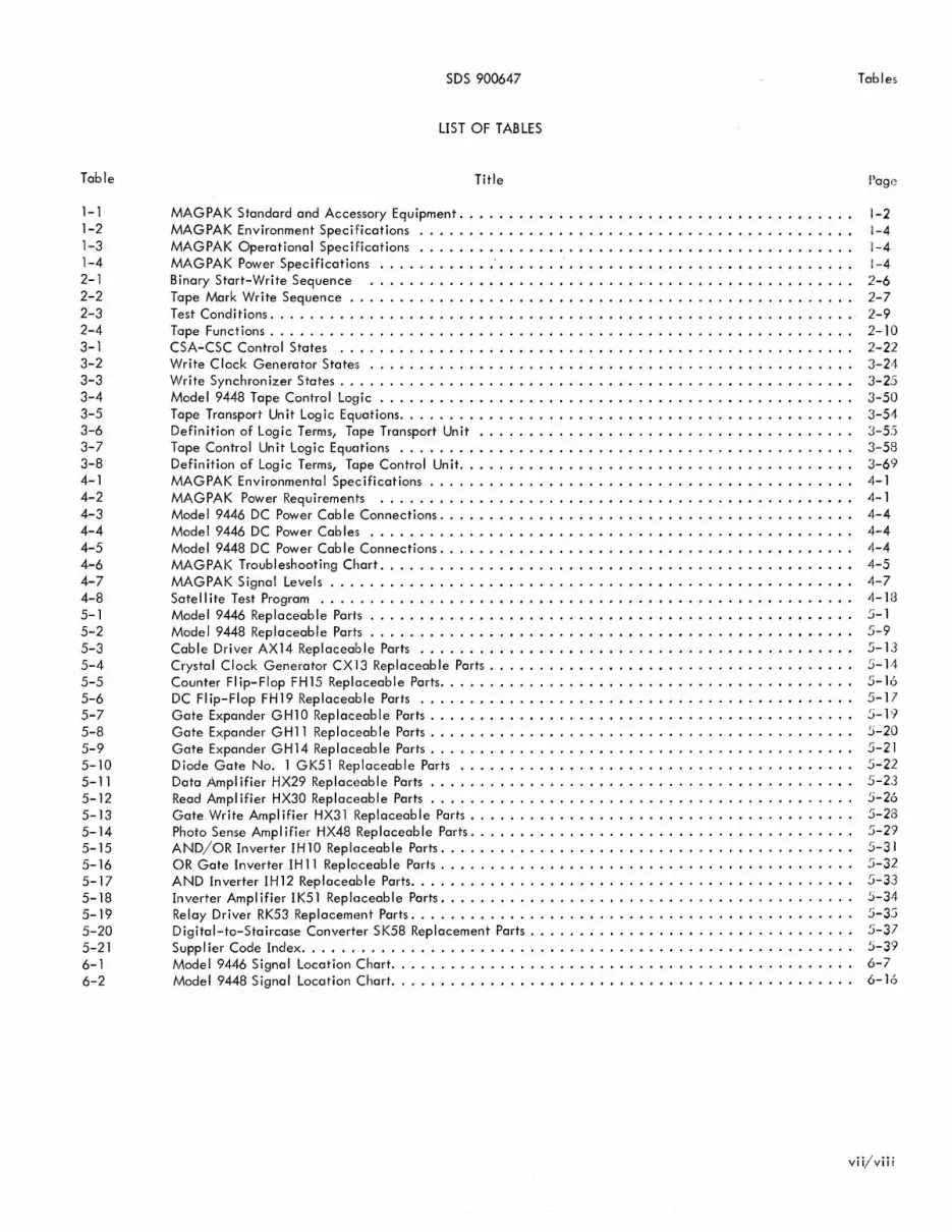
SDS 900647 Tables
LIST OF TABLES
Table Title Page
1-1 MAGPAK Standard and Accessory Equipment. . . . . . . . . . . . . . . . . . . . . . . . . . . . . . . . . . . . . . .. 1-2 1-2 MAGPAK Environment Specifications . . . . . . . . . . . . . . . . . . . . . . . . . . . . . . . . . . . . . . . . . . .. 1-4 1-3 MAGPAK Operational Specifications .............•...... . . . . . . . . . . . . . . . . . . . . . . .. 1-4 1-4 MAGPAK Power Specifications ................................................. ~-4 2-1 Binary Start-Write Sequence ...........•..................................... 2-6 2-2 Tape Mark Write Sequence . . . . . . . . . . . . . . . . . . . . . . . . . . . . . . . . . . . . . . . . . . . . . . . . . .. 2-7 2-3 Test Conditions. . . . . . . . . . . . . . . . . . . . . . . . . . . . . . . . . . . . . . . . . . . . . . . . . . . . . . . . . .. 2-9 2-4 Tape Functions. . . . . . . . . . . . . . . . . . . . . . . . . . . . . . . . . . . . . . . . . . . . . . . . . . . . . . . . . .. 2-10 3-1 CSA.;.CSC Control States .................................................... 2-22 3-2 Write Clock Generator States ............................. . . . . . . . . . . . . . . . . . . .. 3-24 3-3 Write Synchronizer States. . . . . . . . . . . . . . . . . . . . . . . . . . . . . . . . . . . . . . . . . . . . . . . . . . .. 3-25 3-4 Model 9448 Tape Control Logic . . . . . . . . . . . . . . . . . . . . . . . . . . . . . . . . . . . . . . . . . . . . . . .. 3-50 3-5 Tape Transport Unit Logic Equations. . . . . . . . . . . . . . . . . . . . . . . . . . . . . . . . . . . . . . . . . . . . .. 3-54 3-6 Definition of Logic Terms, TClpe Transport Unit . . . . . . . . . . . . . . . . . . . . . . . . . . . . . . . . . . . . .. 3-55 3-7 Tape Control Unit Logic Equations . . . . . . . . . . . . . . . . . . . . . . . . . . . . . . . . . . . . . . . . . . . . .. 3-58 3-8 Definition of Logic Terms, TClpe Control Unit. . . . . . . . . . . . . . . . . . . . . . . . . . . . . . . . . . . . . . .. 3-69 4-1 MAGPAK Environmental Specifications . . . . . . . . . . . . . . . . . . . . . . . . . . . . . . . . . . . . . . . . . .. 4-1 4-2 MAGPAK Power Requirements ................................................ 4-1 4-3 Model 9446 DC Power Cable Connections. . . . . . . . . . . . . . . . . . . . . . . . . . . . . . . . . . . . . . . . .. 4-4 4-4 Model 9446 DC Power Cables ....... . . . . . . . . . . . . . . . . . . . . . . • . . . . . . . . . . . . . . . . . .. 4-4 4-5 Model 9448 DC Power Cable Connections. . . . . . . . . . . . . . . • . . . . . . • . . . . . . . . . . . . . . . . . .. 4-4 4-6 MAGPAK Troubleshooting Chart. . . . . . . . . . . . . . . . . . . . . . . . . . . . . . . . . . . . . . . . • . . . . . .. 4-5 4-7 MAGPAK Signal Levels. . . . . . . . . . . . . . . . . . . . . . . . . . . . . . . . . • . . . . . . . . . . . . . . . . . •. 4-7 4-8 Satellite Test Program ...............•......•...................•........... 4-18 5-1 Model 9446 Replaceable Parf's . . . . . . . . . . . • . . . . . . . . . . . . • . • . . . . . . . . . . • . . . • . • . . . .. 5-1 5-2 Model 9448 Replaceable Parts. . . . . . . . . . . . . . • . . . . . . . . . . . . . . . . . . . . . . • . . . . . • . . . .. 5-9 5-3 Cable Driver AX14 Replaceable Parts ...............•.............. . . . . . . . . . . . . .. 5-13 5-4 Crystal Clock Generator CX'13 Replaceable Parts. . . . . . . . . . . . • . . . . . . . . . . . . . . . . . . . . . . .. 5-14 5-5 Counter FI ip-Flop FH 15 Replaceable Parts. . . . . . . . . . . . . . . . • . . . . . . . . . . . . . . . . . . . . . . . .. 5-16 5-6 DC Flip-Flop FH19 Replaceable Parts .. . . . . . . . . . . . . . . . . . . . . . . . . . . . . . . . . . . . . . . . . .. 5-17 5-7 Gate Expander GH10 Replaceable Parts. . . . . . . . . . . . . . . . . . . . . . . . . . . . . . . . . . . . . . . . . .. :)-19 5-8 Gate Expander GH11 Replaceable Parts. . . . . . . . . . . . . . . . . . . . . . . . . . . . . . . . . . . . . . . . . .. 5-20 5-9 Gate Expander GH14 Replaceable Parts. . . . .. . . . . . . . . . . . . . . . . . . . . . . . . . . . . . . . . . . . .. 5-21 5-10 Diode Gate No. 1 GK51 Replaceable Parts ............... . . . . . . . . . . . . . . . . . . . . . . . . .. 5-22 5-11 Data Amplifier HX29 Replaceable Parts. . . . . . . . . . . . . . . . . . . . . . . . . . . . . . . . . . . . . . . . . .. 5-23 5-12 Read Amplifier HX30 Replaceable Parts. . . . .. . . . . . . . . . . . . . . . . . . . . . . . . . . . . . . . . . . . .. 5-26 5-13 Gate. Write Ampl ifier HX31 Replaceable Parts. . . . . . . . . . . . . . . . . . . . . . . . . . . . . . . . . . . . . .. 5-28 5-14 Photo Sense Ampl ifier HX48 Replaceable Parts.. . . . . . . . . . . . . . . . . . . . . . . . . . . . . . . . . . . . .. 5-29 5-15 AND/OR Inverter IHlO Reploceable Parts. . . . . . . . . . . . . . . . . . . . . . . . . . . . . . . . . . . . . . . . .. 5-31 5-16 OR Gate Inverter IH 11 Replclceable Parts. . . . . . . . . . . . . . . . . . . . . . . . . . . . . . . . . . . . . . . . .. ':'>-32 5-17 AND Inverter IH12 Replaceable Parts. . . . . . . . . . . . . . . . . . . . . . . . . . . . . . . . . . . . . . . . . . . .. ':'>-33 5-18 Inverter Amplifier IK51 Reploceable Parts .......................................... ':'>-34 5-19 Relay Driver RK53 Replacement Parts. . . . .. . . . . . . . . . . . . . . . . . . . . . . . . . . . . . . . . . . . . . .. ':'>-3.3 5-20 Digital-to-Staircase Converter SK58 Replacement Parts. . . . . . . . . . . . . . . . . . . . . . . . . . . . . . . .. 5-37 5-21 Suppl ier Code Index. . . . . . . . . . . . . . . . . . . . . . . . . . . . . . . . . . . . . . . . . . . . . . . . . . . . . . .. 5-39 6-1 Model 9446 Signal Location Chart. .. . . . . . . . . . . . . . . . . . . . . . . . . . . . . . . . . . . . . . . . . . . .. 6-7 6-2 Model 9448 Signal Location Chart. . . . . . . . . . . . . . . . . . . . . . . . . . . . . . . . . . . . . . . . . . . . . .. 6-16
vii/viii


SDS 900647 P€lragraphs 1 -1 to 1 - 1 8
SECTION I
GENERAL DESCRIPTION
1-1 INTRODUCTION
1-2 SCOPE OF MANUAL
1-3 This manual describes the Model 9446/9448 MAGPAK Serial Magnetic Tape System, which is designed and manufacturedby Scientific Data Systems, Santa Monica, California. It includes equipment specifications, operating and programming instructions, theory of operation, installation cmd maintenance procedures j , and detai led drawings of the equipment.
1-4 PURPOSE OF EQUIPMENT
1-5 The MAGPAK Tape System is designed to provide a sequential-access memory device for use with small-tomedium general purpose digital computers. MAGPAK is compact, inexpensive, and simple to opl~rate and maintain. The use of tape cartridges helps el iminate the tape threading problems and sequencing problems inherent with standard magnetic tape, paper tape, and punched c9rd equipment.
1-6 TYPICAL APPLICATIONS
1-7 With MAGPAK, the user can operate a complete library of automatic compilers and assemblers with little manual intervention. Using these automatic programming systems, the four MAGPAK tape tracks are frequently organized as follows:
a. Program I ibrary storage (write protected)
b. Temporary storage
c. Object programs
d. Source programs and data or computational results
1-8 PHYSICAL DESCRIPTION
1-9 The MAGPAK Tape System consists of two basic units: the Model 9446 Tape Transport Unit (shown in figure 1-1), and the Model 9448 Tape Control Unit (shown in figure 1-2). From one to four tape transport units can be operated on-I ine with one tape control unit. Information is stored on two Model 9401 Tape Cartridges. Table 1-1 lists standard and accessory equipment for MAGPAK, (md figure 1-2 shows the main system components and accessories.
.1-10 MODEL 9446 TAPE TRANSPORT UNIT
1-11 Model 9446 consists of two separate tape stations mounted on a single panel, and an electronics chassis which is physically located behind the transports and is part of the transport unit assembly. The left tape station (viewed from the front) is usually designated tape station number 1; the right, tape station number 2. Each tape station is completely independent; that is, each contains its own motors, control panel, and electronics.
1-12 Each of the two tape stations has two independent data channels. Each data channel has its own tape track, fi Ie protect switch, and UNIT SELECT switch. The data channels are designated odd and even. The odd channel controls (i..e., UNIT SELECT and file protect) are on the left side of each transport; the even controls, on the right. The odd data channel on the tape is the one nearer the transport casti ngi the even data channel is the one nearer the operator.
1-13 MODEL 9448 TAPE CONTROL UNIT
1-14 Model 9448 consists of three MX60 Mounting Cases assembled as a unitand ready to mountin a standard 19-inch relay rack. Each MX60 holds up to 20 standard SDS circuit module cards. Each mounting case is hinged on its mounting bracket and swings out to provide access to the connectors.
1-15 MODEL 9401 TAPE CARTRIDGE
1 -16 The Mode I 9401 Tape Cartridge conta i ns 600 feet of 1/4-inch Mylar-base magnetic tape. Each tape has two independent information tracks with a capacityof 1.5 mill ion 7-bit characters per track (one character has 6 data bits plus 1 parity bit). Thus, the two tape cartridges on each MAGPAK provide four independent information channels with a total storage capacity of six mi \I ion characters. At a packing density of 200 characters per inch and a tape speed of 7.5 inches per second, the data transfer rate is 1500 characters per second.
1-17 SPECIFICATIONS
1-18 Environmental, operational, and power specifications for MAGPAK are given in tables 1-2, 1-3, and 1-4, respectively. Input/output specifications (signal levels, impedances, timing, etc.) for SDS 900 Series Computers are given in two brochures, SDS 910/920 Input/Output (publ ication number 64-02-098), and SDS 925/930/9300 Input/Output (publ ication number 64-03-14B).

t.£ ~-::T- - t) 00 {)4It/ ,/,,-, ;"S£,9"P CJ k.. LE".c-T- FUEAI - C!J k. SDS 900647
Table 1-1. MAGPAK Standard and Accessory Equipment
ifjI,lfl - (JOO
~#4r;JKjrF
1-2
Model No.
9292
9293
9401
9402
9403
9446
9448
92360
Description Part No.
Spare Parts Kit for 9448 (optional) 115658
Spare Parts Kit for 9446 (optional) 115660
Tape Cartridge (standard; 2 furnished 107565
per 9446)
Dust-Cover Housing (optional; for 108856
9446 when table-mounted
Tape Cartridge Six-Pack (optional; 114049
replaces six 9401 IS)
Tape Transport Unit (standard) 107636
Tape Control Unit (standard) 107550
Table (optional; for mounting up to 107543
two 9446 l s)
Figure 1-1. MAGPAK Tape Transport Unit
900647B.1

SDS 900647
Model 9448 Tape Control Unit
M~ust-Cover Housing
Model 9446 Tape Transport Un it
Model 92360 Table
Figure 1-2. MAGPAK System Components and Accessories
,I ,I
II II
,,' 'I
900641B.2
1 -3

1-4
Item
Ambient Temperature
Relative Humidity
Altitude
Shock and Vibration
Item
Tape Cartridge
Tape Speed (Read/Write)
Tape Speed (Rewind)
Tape Drive
Recording Method
Recording Format
Inter-Record Gap
Recording Density
Character Read/Write Rate
Tape
Read/Write Head
Beginning-of-Tape Sensing
End-.Qf-Tape Sensing
SDS 900647
Table 1-2. MAGPAK Environmental Specifications
Specification
Operating Environment Non-Operating Environment
100
to 400
C (500
to 1 040
F) _500
to +750 C (_580 to +167°F)
20 to 80% o to 98% (no condensation)
o to 12, 000 feet o to 40, 000 feet
Per commercial data pro- Per commercial van and air cessing installations freight shipments
Table 1-3. MAGPAK Operational Specifications
Specification
SDS Model 9401
7.5 ips
Less than 2 minutes to rewind 600 feet
Capstan/pressure-roller with mechanical storage
Saturation/frequency doubl i ng
Single channel serial; 6 bits plus parity; self-clocking; 2 channels addressable per tape station
3/4 inch
1400 bit per inch (200 characters per inch)
1500 characters per second
1/4-inch wide, 600-ft long, 1-mi I th ick, Mylar base
Two-channel, dual gap
Clear section of tape photosensing
Reflective marker photosensing
Table 1-4. MAGPAK Power Specifications
Item Specification
Model 9446 Model 9448
115 vac ± 10%, 60 ±3 cps 2.0 amp
+50 vdc 0.4 amp
+25 vdc 1. 0 amp 3.4 amps
+ 8 vdc 1.6 amps 1.6 amps
-25 vdc 0.2 amp 0.4 amp
SDS 900647 Paragraphs 1-19 to 1-21
1-19 FUNCTIONAL DESCRIPTION
1-20 MAGPAK performs all of the functions of high-speed, IBM-compatible, magnetic tape units, and uses the same instruction se1'. Programs written for MAGPAK and those written for standard magnetic tape units are identical. The basic difference between MAGPAK and a "big tape" unit is in the method of recording. The high-speed tape unit records seven tracks simultaneously in parallel; MAGPAK records one track at a time, serially.
1-21 A MAGPAK Tape System provides the following features which are also found on the standard high-speed tape systems: binary or BCD coding; recording formats of
one, two, three, or four characters per word; a readafter-write check performed on all writing operations; record keys examined without stopping the tape, searching for a given record and detecting end-of-file records in either forward or reverse; each data channel independently file protected.
1-5/1-6


SDS 900647 Paragraphs 2-1 to 2-27
SECTION II
OPERATION AND PROGRAMMING
2-1 OPERATING INSTRUCTIONS
2-2 CONTROLS AND INDICATORS
2-3 The MAGPAK manual control panel shown in figure 2-1 provides for mode selection, local control of tape motion, and indications of unit status. All tape transport unit controls are interlocked so that no sequencing of control panel switches or commands from the tape control unit will cause damage to the equipment. The indicators correspond to the tape unit status and indicate the tape unit response upon interrogation from the computer.
2-4 AUTO-MANUAL Switch
2-5 The AUTO-MANUAL switch is a twc::>-position toggle switch that is used to select either the automatic or manual mode of operation. In the AUTO position, tape unit functions are controlled by the computer. In the MANUAL position, they are controlled by pushbuttc::>ns on the manual control panel. The FORWARD, REVERSE, and REWIND pushbuttons are inoperative in the automatic mode.
2-6 UNIT SELECT Switches
2-7 The UNIT SELECT ODD and UNIT SELECT EVEN switches are nine-position rotary switches that permit the operator to designate numbers 0 through 7 as the unit numbers of the odd and even data channels used in the system. When the system is in the automatic modEl, a tape unit will respond on Iy to computer commands whose address bits correspond to its UNIT SELECT switch settings. An OFF position is provided to prevent selection of unwanted channels.
2-8 FORWARD Pushbutton
2-9 The FORWARD pushbutton operates in the manual mode to move tape forward (left to right) at 7.5 ips. Forward tape motion stops when load point is encountered, or when the end-of-tape marker is encountered in the manual mode.
2-10 REVERSE Pushbutton
2-11 The REVERSE pushbutton operates in the manual mode to move tape reverse (right to left) at 7.5 ips. Reverse tape motion stops when load point is encountered.
2-12 REWIND Pushbutton
2-13 The REWIND pushbutton operates in the manual mode to move tape in the reverse direction (right to left) at
rewind speed (less than two minutes are required to rewind 600 feet of tape). Rewind motion stops when load point is encountered.
2-14 STOP Pushbutton
2-15 The STOP pushbutton can be used in either the manual or automatic modes to stop tape motion. It directly resets the motion flip-flops.
2-16 RESET Pushbutton
2-17 The RESET pushbutton is used to clear a fault condition or to obtain a ready condition after loading a new tape cartridge. When a tape unit is in a non-ready condition, the capstans do not rotate and (if the unit is in automatic) the READY indicator is not lit. Pressing the RESET button wi II place the unit in operation.
2-18 FILE PROTECT Indicators
2-19 The FILE PROTECT ODD and FILE PROTECT EVEN indicators are I it when no writing is possible on the odd or even data channels of a particular transport. This means that information on a specified tape track cannot be erased inadvertently. There is a FILE PROTECT indicator for each data channel.
2-20 LOAD POINT Indicator
2-21 The LOAD POINT indicator is lit whenever the tape is positioned such that the beginning-of-tape clear space is being sensed.
2-22 END OF TAPE Indicator
2-23 The END OF TAPE indicator is lit whenever the tape is positioned on or past the end-of-tape reflective marker.
2-24 READY Indicator
2-25 The READY indicator is I it whenever a tape is in automatic and is avai lable for use under computer control. When a tape unit is in use, is in the manual mode, or a fault condition exists, the READY indicator is off.
2-26 TURN ON/TURN OFF PROCEDURES
2-27 Power for MAGPAK is turned on or turned off when the computer cabinet power supply is turned on or off. The MAGPAK tape system has no independent power supply; it uses standard computer power levels. Power sequencing is
2·1
Paragraphs 2-28 to 2-32 SDS 900647
0 0 0 0 0 FILE PROTECT LOAD POINT READY END OF TAPE FILE PRO TECT
ODD EVEN
3 @ 0 3 AUTO MANUAL
0 6 RESET 0 6
UNIT SELECT 0 0 0 0 UNIT SELECT ODD EVEN
FORWARD STOP REVERSE REWIND
900647B.3
Figure 2-1. MAGPAK Manual Control Panel
self-contained and no detrimental condition will occur under any combination of power sequencing-control panel operation.
2-28 To prepare MAGPAK for operation, refer to figure 2-2 and perform the following steps:
a. Apply power to computer cabinet.
b. Place AUTO-MANUAL switch on control panel in MANUAL.
c. Set UNIT SELECT switches on control panel to the desired unit number setting.
d. Place load lever in LOAD position.
e. Load tape cartridge on transport as explained in paragraph 2-29 .
f. Return load lever to RUN position.
g. Press RESET button on control panel.
h. Press FORWARD button on control panel. Tape wi II run forward to load point and stop.
i. Press FORWARD button again and allow unit to run forward severa I feet. Press STOP button.
i. Press REVE RSE button; tape will stop near the physical beginning of the load point clear space.
k. Place AUTO-MANUAL switch on control panel in AUTO. The READY indicator should light indicating the un i tis ready to operate under computer contro I.
2-2
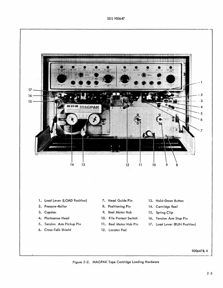
2-29 TAPE CARTRIDGE LOADING PROCEDURE
2-30 Proper loading of the tape cartridge wi II help ensure satisfactory performance of MAGPAK. It is also important that only tape cartridges that conform to SDS Specification No. 108673 be used. The conventional, audio-type cartridges that are commercially available are not controlled to as high a qual ity standard as are SDS Model 9401 Tape Cartridges. Therefore, it is suggested that Model 9401 cartridges be used.
2-31 If possible, each new cartridge used should be wound to the end and rewound to the beginning to ensure that the tape is winding evenly and is centered on the cartridge reel. If any difficulty is encountered in tape winding, refer to section IVof this manual, "Tape Cartridge Fit Ad iustments. II
2-32 The tape cartridge should load and unload freely. Tape should not bind on any tape guide surface. The parts which contact the tape during loading (the read/write head, crosstalk shield, head guide pins, capstans, and photosense head) are beveled so that tape should guide into proper position without damage. The pressure-rollers and tension arms are retracted by the load lever during loading so that they clear the tape.
Note
When loading a tape cartridge, be careful not to touch the oxide (upper) surface of the tape. Skin oils or dust on the tape can cause reqd/write malfunctions. The tape should be fully wound on either reel to prevent marking the data portions of the tape.
17
16
15
l.
2.
3.
4.
5.
6.
SDS 900647
14 13 12
Load Lever (LOAD Position) 7. Head Guide Pin
Pressure-Roller 8. Positioning Pin
Capstan 9. Reel Motor Hub
Photosense Head 10. File Protect Switch
Tension Arm Pickup Pin 11. Reel Motor Hub Pin
Cross-Talk Shield 12. Locator Pad
11 10
13.
14.
15.
16.
17.
9 8
Hold-Down Button
Cartridge Reel
Spring Clip
Tension Arm Stop Pin
3
4
5
6
7
Load Lever (RUN Position)
900647B.4
Figure 2-2. MAGPAK Tape Cartridge Loading Hardware
2-·3

Paragraphs 2-33 to 2-49 SDS 900647
2-33 See figure 2-2 for identification of transport hardware associated with loading and unloading. To load the tape cartridge, perform the following steps:
a. Move load lever clockwise to load detent (LOAD position) .
b. While holding cartridge in hand, rotate cartridge reels to tighten tape between reels.
c. Place notch in bottom of cartridge over nylon hold-down button shaft at bottom of transport; push cartridge down so that shaft slides into notch. Downward motion wi II stop when cartridge contacts the two positioning pins located on either side of the hold-down button.
d. Maintaining a downward pressure on cartridge to keep it against positioning pins, push the top forward between the spring cl ips until it snaps "home ll against locator pads. Cartridge must be seated firmly against locator pads.
e. Move load lever counterclockwise to RUN position.
f. Rotate cartridge reels by hand slightly so that reel motor hub pins engage cartridge reels. There are two pins per hub; both must be engaged or tape will not wind properly. The tape cartridge is now ready to operate.
2-34 TAPE CARTRIDGE UNLOADING PROCEDURE
2-35 It is very important that the tape be run to the physical beginning-of-tape before the cartridge is removed from the transport., Th is ensures that any tape damage that might have occurred during loading or unloading of a cartridge will be confined to the section of tape between the load point marker and the physical beginning-of-tape. This section of tape is not used for information storage.
2-36 See figure 2-2 for identification of transport hardware associated with loading and unloading. To remove a cartridge from the transport, perform the following steps:
a. Run tape to physical beginning-of-tape and stop.
b. Move load lever clockwise to LOAD position.
c. Pull top of cartridge away from transport and lift cartridge out of hold-down apparatus.
2-37 PLACEMENT OF FILE PROTECT (WRITE) PLUGS
2-38 If a data channel is to be file protected, then a write plug (SDS 108784) should not be inserted between the fi Ie protect switch lever and the bottom of the tape cartridge. Conversely, if a data channel is to be written on, then a write plug should be inserted in the cartridge corresponding to the channel to be written. To enable writing on the odd channel, insert a write plug in the bottom left cavity of the cartridge (viewed from the front); to enable writing on the even channel, insert a write plug in the bottom right cavity of the cartridge.
2-4
2-39 PLACEMENT OF LOAD-POINT CLEAR SPACE AND END-OF-TAPE MARKERS
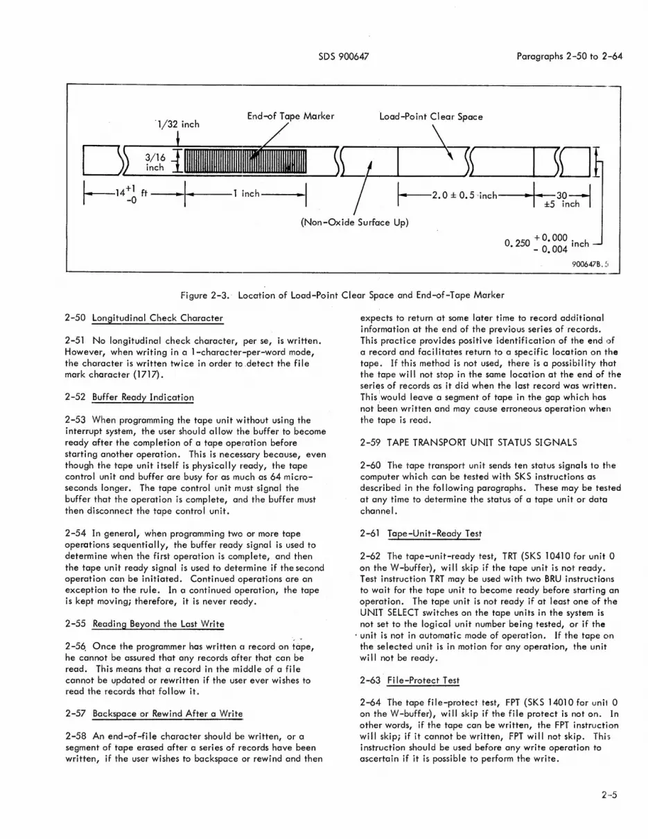
2-40 As shown in figure 2-3, a reflective marker strip is placed on the non-oxide surface of the tape approximately 14 feet from the end of the reel to indicate end-of-tape. IBM 352407 Reflective Tape, or equivalent, should be used for this marker. A clear section of tape (one with the oxide removed) is located approximately 30 inches from the beginning of the reel to indicate load-point.
2-41 PROGRAMMING
2-42 INTRODUCTION
2-43 The basic programming to write or read information on any magnetic tape device (including MAGPAK) is essentially the same as for any input/output device with or without interlace control. However, magnetic tape in general (and MAGPAK in particular) is also used as an external storage device rather than strictly an input or output device. Therefore, certain functions which are unique to programming for magnetic tape systems are presented in detail in this section. Note that all functions that can be performed on a standard high-speed tape unit (such as SDS Model 9248) can be performed on MAGPAK.
2-44 Without-Leader EOM Instructions
2-45 As a general rule, all EOM instructions to the tape units should specify start-without-Ieader. Since the tape unit generates gap on all write operations automatically, it is not necessary for the starting EOM to call for leader. A leader instruction should never be included in a magnetic tape program because the buffer wi II then attempt to generate leader, and an erroneous operation may occur.
2-46 Four-Character Mode
2-47 As a general rule, tape units should be programmed for four characters per word if possible. (The write-tapemark operation is an exception to this rule.) It is possible to write tape in a 1-, 2-, or 3-character-per-word mode provided the buffer can be kept suppl ied with characters at a sufficient rate. On reading, however, the tape unit uses the buffer character count to ascertain when it has read two characters and can look for gap. If a 1-character-per-word read were started, a single noise character would stop the tape. All scan operations must be in 3- or 4-characterper-word mode or the tape wi II not stop when it reaches gap.
2-48 Timing Considerations
2-49 The Tape Control Unit is designed such that there are no timing restrictions on programming the tape unit. The programmer need only concern himself with ascertaining that the unit is ready before he gives a start command.
SDS 900647 Paragraphs 2-50 to 2-64
End-of Tape Marker '1/32 inch II
i Load-Point Clear Space
(Non-Oxide Surface Up)
O 250 + o. 000. h • _ 0.004 inC
900647B. :'
Figure 2-3. Location of Load-Point Clear Space and End-of-Tape Marker
2-50 Longitudinal Check Character
2-51 No longitudinal check character, per se, is written. However, when writing in a l-character-per-word mode, the character is written twice in order to .detect the file mark character (1717).
2-52 Buffer Ready Indication
2-53 When programming the tape unit without using the interrupt system, the user should allow the buffer to become ready after the completion of a tape operation before starting another operation. This is necessary because, even though the tape unit itself is physically ready, the tape control unit and buffer are busy for as much as 64 microseconds longer. The tape control unit must signal the buffer that the operation is complete, and the buffer must then disconnect the tape control unit.
2-54 In general, when programming two or more tape operations sequentially, the buffer ready signal is used to determine when the first operation is complete, and then the tape unit ready signal is used to determine if the second operation can be initiated. Continued operations are an exception to the rule. In a continued operation, the tape is kept moving; therefore, it is never ready.
2-55 Reading Beyond the Last Write , ~
2-56. Once the programmer has written Cl record on tape, he cannot be assured that any records after that can be read. This means that a record in the middle of a file cannot be updated or rewritten if the user ever wishes to read the records that follow it.
2-57 Backspace or Rewind After a Write
2-58 An end-of-fi Ie character should bE~ written, or a segment of tape erased after a series of r,ecords have been written, if the user wishes to backspace or rewind and then
expects to return at some later time to record additional information at the end of the previous series of records. This practice provides positive identification of the end of a record and facil itates return to a specific location on the tape. If this method is not used, there is a possibility that the tape wi II not stop in the same location at the end of the series of records as it did when the last record was written. Thiswould leave a segment of tape in the gap which has not been written and may cause erroneous operation when the tape is read.
2-59 TAPE TRANSPORT UNIT STATUS SIGNALS
2-60 The tape transport unit sends ten status signals to the computer which can be tested with SKS instructions as described in the following paragraphs. These may be tested at any time to determine the status of a tape unit or data channel.
2-61 Tape-Unit-Ready Test
2-62 The tape-unit-ready test, TRT (SKS 10410 for unit 0 on the W-buffer), will skip if the tape unit is not ready. Test instruction TRT may be used with two BRU instructions to wait for the tape unit to become ready before starting an operation. The tape unit is not ready if at least one of the UNIT SELECT switches on the tape units in the system is not set to the logical unit number being tested, or if the
. unit is not in automatic mode of operation. If the tape on the selected unit is in motion for any operation, the unit will not be ready.
2-63 Fi Ie-Protect Test
2-64 The tape fi Ie-protect test, FPT (SKS 1401 0 for unit 0 on the W-buffer), will skip if the file protect is not on. In other words, if the tape can be written, the FPT instruction will skip; if it cannot be written, FPT will not skip. This instruction should be used before any write operation to ascertain if it is possible to perform the write.
2-5
Paragraphs 2-65 to 2-83 SDS 900647
2-65 Beginning-of-Tape Test
2-66 The beginning-of-tape {or load-point} test, BTT {SKS 12010 for unit 0 on the W-buffer}, will skip if the tape is not positioned at load point. This instruction can be used to determine when or if the tape is rewound.
2 -67 End -of -Tape Test
2-68 The end-of-tape test, ETT (SKS 11010 for unit 0 on the W-buffer), wi II skip if the tape is not at the end-oftape marker. It should be used after every write operation to determine when the end-of-tape is reached.
2-69 Density Tests
2-70 MAGPAK always responds 200 bpi to a density test interrogation. It will not skip on the 200 bpi-test, DT2 (SKS 16210 for unit 0 on the W-buffer). It wi II always
. skip on the high-density tests, DT5 (SKS 16610 for unit 0 on the W-buffer) and DT8 (SKS 17210 for unit 0 on the W-buffer).: "Big tape" units on the same channel will test in the normal manner.
2-71 End-of-File Test
2-72 Tape end-~f-file test, TFT (SKS 13610 for all tape units on the W-buffer), will not skip if the tape read or scan operation last completed did not encounter a tape mark. The Tape Control Unit wi II detect a recorded tape mark and signal end-of-file after any read or scan operation in either the forward or reverse direction. This signal should be tested until the completion of the operation because the end-of-fi Ie signal wi II be true unti I some character, other than the tape mark, is read. The end -of -fi I e test is a Tape Control Unit signal, rather than a Tape Transport Unit signal. Therefore, any unit address may be used to test the control unit.
2-73 Gap Test
2-74 The tape gap test, TGT (SKS 12610 for any tape on the W-buffer), will skip as long as the tape is not in motion in the gap following a record written or read. When the tape unit has detected the gap at the end of a record, it will generate the gap signal. This signal will remain true for approximately ten mill iseconds. During this time, the test instruction wi II not skip and the tape may be given a command to continue in the direction it is going. If so programmed, the tape wi II continue without stopping.
2-75 If the record encountered should be an end-of-fi Ie, the gap signal will not become true, and the tape will always stop. Like the end-of-fi Ie test, the gap test is a control unit test and any tape unit address may be used.
2-76 Skip If Not MAGPAK
2-77 The skip if not MAGPAK test MPT (SKS 1021 n) skips if the selected unit is not MAGPAK.
2-6
2-78 WRITING
2-79 Introduction
2-80 Writing on magnetic tape is essentially the same as outputting information to any other output device, with or without the interlace to control data transfer. The program should first determine that the desired logical unit is ready
and that the file protect is off. Interlace may be controlled, then set up, and the write-tape-binary 0NTBW or WTBY} is executed. The interlaced buffer then governs transfer of data to the tape. A typical binary start-write sequence, with tape unit No.6 connected to the W-buffer, is shown in table 2-1.
Table 2-1. Binary Start-Write Sequence
Memory Instruction Location Code Mnemonic Remarks
01000 00250000 EOM* START 10000 Alert the interlace
01001 00210000 EOM 10000 Set two high-order count bits
01002 01301040 POT CW Send con-trol word to interlace
01003 00203656 WTBW 6, 4 Start write
01040 20004000 OCT CW 20004000 Control word, 256 words starting at 4000
*The EOM in location 1001 is not needed to write a record of 256 words, but is there merely to illustrate the genera I case.
2-81 The buffer will automatically terminate its output when the interlace word count is reduced to zero. If the interrupt system is enabled, an 12 (33 or 32) interrupt will be generated when the tape is stopped.
2-82 Write Errors
2-83 If the read-after-write check finds a character parity error, the buffer error flip-flop is set and can be tested with a BET instruction (SKS 20010 for the W-buffer). If there was an error detected on writing, the program should erase backward over the record, then space backward over the

SDS 900647 Paragraphs 2-84 to 2-100
previous record. The previous record is spaced over in a forward direction (or read) and then a rewrite of the previous record may be attempted.
2-84 If the second attempt is also in error, an erase backward - space backward over previous record - space forward over previous record - erase bad section of tape -rewrite routine should be executed. The procedure is continued until the record is correctly written. An erase backward - attempt rewrite routine is !lQ.:t recommended.
2-85 Long-term speed variations can cause the write head to be mispositioned such that the block is not completely erased or the previous inter-record gap is shortened each cycle. Both conditions can cause a tape to be written such that subsequent reading cannot be accompl ished.
2-86 A space backward - attempt rewrite routine is not recommended since the write error may have been caused by gap-in-data. A spacing backward sequence could terminate from the gap-in-data location instead of the beginning of record. This may also have the result of not being able to read the information.
2-87 Writing From the Load Point MarkElr
2-88 It is desirable to erase approximately 3 to 3.5 inches of tape before writing the first record when the tape is situated at the load point. An erase operation for 150 words will clear the desired section. This procedure is particularly important if the previous recording history of the cartridge is unknown.
2-89 Writing Near the End of Tape
2-90 About '14 feet of tape is usually reserved between the end-of-tape marker and the physical end of tape. This space contains at least 12 feet of usable tape. When the end-of-tape marker is sensed, there is sufficient tape remaining to record 28,800 characters.
2-91 End-of-Fi Ie Definition
2-92 An end-of-fi Ie record is defined as a tape mark character 1717. The end-of-file is detected by reading the tape mark. An end-of-file is used to indicate the end of a group of related records or the end of recorded i nformation on a tape.
2-93 Writing the Tape Mark
2-94 The tape mark is a 1-character BCD record regardless of the parity of the previous information I:>n the tape. (Actually, MAGPAK always writes in binary, regardless of
the command given. The file mark is written in BCD in order to maintain program compatibil ity with standard magneti c tape systems. ) To start the wri te process, an EOM instruction for one character per word in BCD should be given. This is followed by an MIW instruction to load a word into the buffer wh ich contains 17XXXXXX (the 17 is the tape mark). The MIW is followed by a terminate output. As in any write operation, when the buffer is ready or when the 12 interrupt occurs, the operation is complete. For example, to write a tape mark on tape un it 3, the sequence in table 2-2 should be used
Table 2-2. Tape Mark Write Sequence
Memory Instruction Location Code
02000 00202053
02001 01202100
02002 00214000
02100 17000000
2-95 ERASING
2-96 Introduction
Mnemonic
WTDW START
MIW
TOPW
OCT TMC
"~
Remarks
"-3, 1 Write 1
character/ word, BCD
TMC Output tape mark constant
. Terminate output
.. -17000000 Tape mark
constant
2-97 The erase tape operation is essentially equivalent to writi ng information except that no data are recorded on tape. The erase is timed like a write operation in that the inter lace (or equivalent) is used to supply dummy characters to the buffer and allows the tape unit to clock the desired number of character times for the I ength of tape to be erased.
2-98 Erasing a Record After a Write Error
2-99 When a write erroroccurs, an erase in reverse should be used to back up to the beginning of the record. This is accompl ished by setting up the interlace (or equivalent) exactly as was done for the preceding write operation, and executi ng an erase tape reverse, ET RW or ET RY (EOM 07670for unit Oon theW-buffer). Terminationof the erase is the same as thatfor a write; when the operation is complet~ an 12 (33 or 32) interrupt occurs and the buffer is ready.
2-100 If a record cannot be rewritten, the user should erase it completely and try again on a new section of tape. This is accomplished by first erasing in reverse to the beginning of the record, and then erasing forward for the same number of words as was programmed for the original write or reverse erase. This is programmed the same as a reverse erase except that a normal erase tape instruction, ETW or ETY (EOM 06670 for unit 0 on the W-buffer) is used.
21

Paragrap~s 2-101 to 2-118 SDS 900647
2-101 Erasing a Given Length of Tape
2-102 To erase a fixed section of tape, it is only necessary to calculate the number of words that must be sent to the buffer to .clock the erase operation over the desired legnth of tape. An allowance of about 0.45 inch should be made for gap that will be written by the tape control unit automatically. A write or erase operation stops when the read head finds the gap at the end of a record. Since the read head is always reading the gap in an erase operation, the tape stops O. 3 inch shorter after forward erase than after a write operation of the same length.
2-103 READING
2-104 Introduction
2-105 Reading from magnetic tape is similar to reading from paper tape. When the tape is ready, a sequence like the one described for magnetic tape writing is executed, except with a read tape rather than a write tape EOM instruction~ The tape wi II start and the interlace (if used) wi II store information in memory.as the buffer fi lis. When the gap is encountered, the gap signal will come true; if another read tape command is given, the tape will continue without stopping. If no second EOM is given, the tape wi \I stop, the buffer wi II become ready, and an 12 (33 or 32) interrupt wi II be generated. The program may then inspect the error indicator in the buffer to determine if a parity error occurred. If an error did occur, then the program should backspace over the record and attempt to reread it. At least 9 reread attempts, for a total of 1 o read tries, should be made before the record is considered bad or unreadable. Usually one reread wi II suffice to read the record correctly.
2-106 Long Records
2-107 If the record is longer in number of words than the word count set in the interlace, the interlace will reach zero before the gap is detected. When the interlace goes to zero, it disengages its control of the buffer and allows normal program control to resume. When the buffer fills again, a'n 11 (31 or 30) interrupt will occur. The programmer:can choose several responses to this condition. Usual procedure would be to execute a skip-remainder-ofrecord EOM (SRRW, 02 13610), empty the buffer with a WIM, then clear the interrupt and return to the main program to await the end of record. If, however, the user wishes to continue to read the remainder of the record, he may reload the interlace and allow it to control the reading of the remaining information.
2-108 Reading an End-of-File
2-109 The tape control unit wi II not generate the gap signal or: an Il interrupt if the program starts the tape in a read operation and the next record is an end of file. The tape wi II stop, the buffer wi II become ready, an 12 i nterrupt is generated, and the end-of-file test wi II not skip
2-8
(TFTW, 40 13610). A BCD record which consists only of 17
8(001111) characters will be considered an end-of-file.
2-11 0 Reading at the End of the Tape
2-111 As in writing, when the end-of-tape marker is encountered, the end-of-tape test will not skip. The user w ill norma II y have an end -of -fil e record after the last recorded information, even if this occurs beyond the endof-tape marker. If preferred, however, it is possible to use the end-of-tape marker to indicate the end of information.
2-112 SCANNING AND SEARCHING
2-113 Introduction
2-114 The scan-tape operation is I ike a non-interlaced read operation except that only one 11 interrupt (buffer full condition) occurs for each record. This occurs when the gap is first encountered and while the tape is still moving. The buffer at that time will contain the last four characters of the record. When scanning forward, this means the last word of the record. When scanning reverse, this means the first word of the record which will be in reverse order by characters. For example, if the first word contained the eight octal digits 01 23 45 67, when this is loaded into the buffer in the reverse scan, it would appear as 67 45 23 01. The position of bits in the character is not modified, only the order of the characters is changed in the word.
2-115 Continued Scan
2-116 Since the 11 interrupt (31 or 30), or buffer full condition, occurs when the gap is reached (but while the tape is still moving), it is possible to give another scan instruction and have the tape continue wean the next record without stopping. The user has ~mi II iseconds from the time of the interrupt to give the continue command to keep the tape in operation. If no instructions are received by the tape control unit during this period, it will bring the tape to a stop in the middle of the gap and generate an 12 interrupt. The tape unit and buffer will then be in ready status.
2-117 Reverse Search
2-118 Searching for a given record that is identified by the first word is a simple application of the repeated scanreverse operation. First, the identifier word should be reversed by character. When the selected tape unit is ready, it is started in reverse scan, SRBW (EOM 07635 for tape un i t 5 on the W -buffer). The program may wa it for the 11 interrupt, or may be suspended on a WIM instruction until the gap is reached and the buffer is filled with the first word of the record. This word is then compared with the reversed identifier for which the search is being made. If they are not equal, the program gives another scanreverse EOM and waits to check the next record. If they are equal, the program does not give any further EOM instructions but merely waits for the 12 interrupt or for the

SDS 900647 Paragraphs 2-119 to 2-136
buffer to be ready. The program may then indicate a forward-read, if desired.
2-119 Forward Search
2-120 A search-forward operation could be executed in the same manner as the reverse search if the identifier. word was recorded at the end of a record, as well as at the beginning. Since this process is somewhat awkward, provision has been made to search forward on the first word of a record and read the information when the desired record is found. This can be easily implemented since the time between words is on the order of 320 cycles (for 8 fJsec cycle time computers).
2-121 The search is accomplished by starting the tape in a forward-read operation, and waiting for the first 11 interrupt (buffer full condition). When this occurs, the identifier word can be compared with the first word of tbe record. If they are not equal, an RTSW instruction (EOM 1400X for tape units on the W-buffer) is given to convert the read operation to scan. When the next 11 occurs, the tape is at the end of the record, and the program may give another read EOM to keep the tape moving and check the next record. If the identifier word and the first record word are equal, the program may go ahead and read the record, either under program control or by settin!~ the interlace.
2-122 Scanning an End-of-Fi Ie Record
2-123 As in the read mode, when an end-of-file record is encountered while scanning, the end-of~fi Ie test wi II not skip. In the scan mode, however, an Il interrupt will occur after the end-of-fi Ie record is encountered and before the tape stops.
2-124 Scanning Near the Beginning of T~
2-125 When scanning in reverse, the det4ection of the loadpoi nt marker wi II cause the tape to be stopped and an 12 (33 or 32) interrupt and buffer ready condition to occur. This is the only time in the scan mode of operation that an 12 interrupt occurs without prior occurrence of an 11 interrupt.
2 -126 Scann i ng N ear the End of Tape
2-127 The end-of-tape detection causes no special action other than the settingof theend-of-tapesignal. If the end of information is not indicated by an end-of-fi Ie record, the program should check the end-of-tape signal before scanning forward over the next record.
2-128 SPACING
2-129 Space Forward or Reverse, One Record
2-130 To space one record, the tape is started forward (or reverse, as desired) in a scan mode and the program waits for the buffer to be ready or for the 12 intefrupt. The 11 interrupt should be ignored by executing a WIM instruction to a dummy location, and then executing the BRU indirectly
to clear the interrupt channel. When the 12 interrupt occurs, or when the buffer is ready, the tape will have been stopped in the gap following the record over which the space was executed.
2-131 Space More Than One Record
2-132 To space more than one record, another scan EOM instruction should be executed when the 11 interrupt occurs indicating the detection of gap. This may be repeated until the desired number of records have been spaced over. The end of fi Ie, however, wi II require special consideration when spacing over a file of unknown length. The user may wish to program a che~k for end of fi Ie when spacing.
2-133 REWI NDI NG
2-134 A tape unit may be started in rewind at any time as long as the unit is ready. This operation does not use the buffer or the tape control unit. Anyor all tape unitsmaybe rewound whi Ie any input/output operation (on tape units or other devices) is in progress. The rewind instruction, REWW, is an EOM (02 14016 for tape unit 6 on the Wbuffer). Once started, the tape wi II continue in rewind until the beginning of tape is sensed. It will then stop.
2-135 SUMMARY OF TAPE OPERATION CODES
2-136 Tables 2-3 and 2-4 contain a summary of operation codes used with the MAGPAK tape system.
Table 2-3. Test Conditions
Mnemonic Description Buffer Coding
TRTW n Skip if tape unit n is W SKS 104111 TRTY n not ready Y SKS 1051 n
FPTW n Skip if tape unit n not W SKS 1041n FPTY n fi I e -protected Y SKS 1411n
BTTW n Skip if tape unit n not W SKS 1201n BTTY n at beginning of tape Y SKS 1211n
ETTW n Skip if tape unit n W SKS1101n ETTY n . not at end of tape Y SKSlllln
DT2W n Skip if tape unit n not W SKS 1621n DT2Y n at 200-bpi density Y SKS 1631 n
DT5W n Skip if tape unit not W SKS 1661n DT5Y n at 556-bpi density Y SKS 1671 n
DT8W n Skip if tape unit not W SKS1721n DT8Y n at 800-bpi density Y SKS 173111
TFTW Skip if not end of fi Ie W SKS 13610 TFTY Y SKS 13710
TGTW Skip if not gap W SKS 12610 TGTY Y SKS 12710
MPTW Skip if unit not W SKS1021n MPTY MAGPAK Y SKS 1031n
-
29
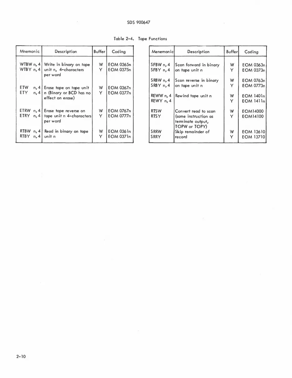
SDS 900647
Table 2-4. Tape Functions
Mnemonic Description Buffer Coding Menemonic Description Buffer Coding
WTBW n, 4 Write in binary on tape W EOM 0365n SFBW n, 4 Scan forward in binary W EOM 0363n WTBY n,4 un it n, 4-characters Y EOM 0375n SFBY n,4 on tape un it n Y EOM 0373n
per word SRBW n, 4 Scan reverse in binary W EOM 0763n
ETW n,4 Erase tape on tape un it W EOM 0367n SRBY n,4 on tape un it n Y EOM 0773n
ETY n,4 n (Binary or BCD has no Y EOM 0377n effect on erase) REWW n, 4 Rewind tape unit n W EOM 1401n
REWY n,4 Y EOM 1411n
ETRW n,4 Erase tape reverse on W EOM 0767n RTSW Con ve rt read to scan W EOM14000 ETRY n,4 tape un it n 4-characters Y EOM 0777n RTSY (same instruction as Y EOM14100
per word term inate output, TOPW or TOPY)
RTBW n,4 Read in binary on tape W EOM 0361n SRRW Skip remainder of W EOM 13610 RTBY n,4 unit n Y EOM 0371n SRRY record Y EOM 13710
2-10

SDS 900647 Paragraphs 3-1 to 3-14
SECTION III
THEORY OF OPERATION
3-1 INTRODUCTION
3-2 Contained in this section is a description of the electromechanical, functional, and logical theory of operation for MAGPAK. In general, the first part of this section deals with the 9446 Tape Transport Unit, and the second part with the 9448 Tape Control Unit. A list of logic equations and a glossary of logic terms for both units are included at the end of this section. Logic diagrams and other reference drawings are incl uded in section V of this manual.
3-3' MAGPAK CODING SCHEME
3-4 In MAGPAK,binary information is recorded serially using a self-clocking frequency-doubl ing scheme. A binary one is recorded as one flux revers4JI in a bit interval, and a binary zero is recorded as two fl ux reversals in a bit interval. Figure 3-1 illustrates a typical pattern.
Time----
1-- Bi t Interva I
o 0 o o
900647B.6
Figure 3-1. MAGPAK Coding Scheme
3-5 There is a flux reversal at the beginning of every bit interval which is used to sychronize the read decoder in playback. If a transition appears near the center of the bit interval, a zero is decoded. If no transition appears midway between synchronizing transitions, a one is decoded. Thus, all of the information is contained in the fl ux reversals. These reversals appear as peaks in the readback waveforms. The read electronics detect the peaks and reconstruct a square-wave signal for the read decoding logic.
3-6 At the beginning of a record, the read decoding logic must first establish synchronism with the recorded bits. A IIpreamable code, II containing a string of logical ones, provides 8 bit times for this action to be completed.
3-7 The read decoding logic must be tolerant of variations in the playback signal which may result from speed variations, magnetic coating variations, drift in the read amplifiers, and noise. Figure 3-2 summarizes the various ti~e
intervals that the read decoding logic appl i es to the interpretation of the read si gnal.
3-8 READ DECODING TIME INTERVALS
3-9 Starting with the first transition at the beginning of each bit time, the read decoding logic generates the timing intervals indicated in figure 3-2. The most important intervals are c and e. If a read signal transition occurs in intervals c, which ranges from 31. 8 I-' sec to 63.6 I-' sec after the first transition, the read decoder interprets the bit as a logical zero. If no transition occurs in interval c, the read decoder interprets the bit as a one.
3-10 Time interval e defines a period from 71.51-' sec to 127 jJsec after the first transition. A read signal transition that occurs during interval e confirms synchronization for the bit under consideration and restarts all timing at zero in preparation for decoding the next bit. If no transition occurs during interval e, the read decoder times into the zone indicated in figure 3-2 as interval f. Once this happens, an overdue transition has been detected and a gap signal is generated by the read decoder.
3-11 The gap signal is interpreted by the control logic in the light of whether a postambl e has occurred, and an error wi II be indicated if the gap appears prematurel y.
3-12 Under the true gap conditions, no signals are presented to the read ampl ifier, and noise may supply spurious transitions to the read decoder. Interval b is the time band from 7. 951-'sec to 31. 81-'sec after a first transition. If a transition in the read signal appears in interval b, the read decoder interprets it as spurious and indicates gap.
3-13 There are two time intervals, a and d, which result from the fact that the read decoder derives all of its timing from a precise reference clock operating at 12 times the nominal bit rate. Interval a is called the sync quantizing interval and defines the first 7.91-' sec after the first transition. If a transition occurs within interval a, it will either be ignored or interpreted as having occurred in interval b, producing an early transition gap signal.
3-14 Time interval d as indicated in figure 3-2 is the decode quantizing interval whi ch spans the 7.91-' sec between interval c and e. A transition that occurs during interval d can be produced only by a very marginal set of reading conditions. Even so, the read decoding logic interprets the transition conservatively. This can be shown by predicating all possible combinations of bit-pairs and clock phasing. From these circumstances only four cases are possible:
3~" 1

Paragraphs 3-15 to 3-20 SDS 900647
l 1 It 1 f t ~t 1 '!t 0 12t 3 '2t 3 4 3
I a I b I c I d I e I 0 7.9 31.8 63.6 71. 5 127
I. ~ec ~ec J.lSec fJSec fJSec
Nominal Bit Time (t) 95.3fJSec.
a. Sync Quantizing d. Decode Quantizing
b. Early Transition Gap Detect e. Sync Confirm
c. Zero Detect f. Overdue Transition Gap Detect
900647B.7
Fi gure 3-2. Read Decoding Time Intervals
a. Tf:Je bits are read correctly, synchronism is maintained, and no error is indicated.
b. The bits are read correctly and synchronism is maintained, but an error is indicated to the computer by the gap logic.
c. The bi ts are read i mproperl y an d an error is indi cated.
d. The read decoder is forced out of synchronism; that is, synchronism may be establ ished on the mi d-bit transitions in logical zeroes. In this case, however, the arrival of the first logi cal one wi II produce a gap error si gnal.
3-15 In summary, the read decoder can retrieve information correct I y and maintain synchronism on signals that have been degraded by'as much as -25% to +33% in time. Further degradation produces detectable errors even though the referen:ce clock for the read decoder is running at only 12 times the nominal bit rate.
3-16 MAGPAK RECORD FORMAT
3-17 Information is recorded on MAGPAK serially in records of consecutive 7-bit characters. The number of characters per word written into a record is variable under program control. The nominal separation or gap between records is 3/4 inch. Inter-record gap is dc-erased by the writing logic.
3-18 Figure 3-3 shows the complete MAGPAK record format. The preamble code, consisting of 8 ones followed by 1 zero, is recorded i ust prior to the first character of each record. An odd parity bit is recorded as the first bit of each character" Immediately following the last character
3-2
in the record, the postamble code is written as 1 zero followed by 8 ones.
3-19 The preamble and postamble codes are symmetrical with respect to the record so that they perform reciprocal functions as the tape is scanned in reverse. These functions may best be explained in the following summary of the reading sequence:
a. As the read head encounters the preamble, the read logic is brought into bit synchronization using the recorded ones as a reference. Only 6 of the bits are metered for validity.
b. The read logic is armed for the zero, after 7 bits are detected, the last of which must be a one. Upon receipt of the preamble zero bit, the read logic commences the character reading process.
c. The 7 bits of each character are read serial I y, checked for odd parity, and converted to character parallel for transmission to the computer.
d. After the last character has been read, the first 7 bits of the postamble code are detected but not transferred to the computer. The read logic is armed to confirm the validity of the postamble.
e. The read logic meters out the remaining two bits of the postamble and then detects gap normally within one bit time.
3-20 The parity test will indicate an error to the computer for all single-bit read errors and a large class of multiplebit errors. If the read logic is out of synchronism with the record format, an error condition will very likely be detected by the parity logic.

SDS 900647 Paragraphs 3-21 to 3-32
Direction of Tape . ..
Gap {II. • • 1 1 1 I 0 16 5 4 3 2 1 P 16
t -aones-l I last J 5 4 iiI P 16 5 4 3 2 1 P 10 11 1 . .. 1 II} Gap
L First I La onesj _ Postamble -'--- Chclracter
Code with Character -'--- Preamble wi~ Code
Odd Parity Odd Parity \
900647B.8
Figure 3-3. MAGPAK Record Format
3-21 It should be noted that of the 128 possible combinations of 7-bit patterns in each character position, 64 are passed as val i d characters and 63 produce parity errors. One combination (0111111) does not produce a parity error directly, inasmuch as it is used to detect the postamble code. A premature appearance of this code produces an error indication by way of the gap detection logic which is described below.
3-22 The recld logic indicates a gap condition whenever an absence of signal or spurious signals are read. If the gap condition is indicated before the postamble code has been detected, an error signal is transmitted to the computer and the control logic stops the tape motion.
3-23 Additional I y, if a read error causes 7 bits of the postamble code (0111111) to appear prematurely as a character, the parity logic will not indicate an error as noted above. The gap condition is examined by the read logic one character time after the postamble is detected; thus if a gap condition does not exist within 4 bit times following the pattern 0111111, the premature postamble is detected as an error.
3-24 TAPE TRANSPORT UNIT ELECTROMECHANICAL DESCRIPTION
3-25 Each Model 9446 Tape Transport Un it consists of two separate tape transports mounted on a single panel, and a transport el ectronics assembly. The tape transports move magnetic tape over the read/write heads; the electronics assembly contains circuitry necessary to control the transports.
3-26 TAPE DRN E SYSTEM
3-27 Forward and Reverse
3-28 Forward and reverse movement of tape is controlled by a conventional capstan-pressure roller system, consisting of a capstan motor, capstans, pressure rollers, and a
drive bel t. Forward and reverse movement is accompl ished as follows: Signals from the computer are sent through the Tape Control Unit to the transport electroni cs. These si g-' nals activate a pressure roller which brings the tape into contact with one of two counter-rotating capstans, clamping the tape between the capstan and pressure roller. Tape is then driven (in the direction determined by the computer command) until the pressure roller is disengaged and the tape stops.
3-29 Capstan Motor and Pulley Hub. Capstan motor M 1 is a 115-vac, 50/60-cps, single-phase, 4-pole, hysteresis synchronous motor which operates continually when relay K2 is cI osed. With 60-cps input, the motor rotates at 1800 rpm; at 50 cps, it rotates at 1500 rpm. As shown in figure 3-4, rotational force is transferred to the drive belt by a steel pulley hub attached to the motor shaft. A larger pull ey hub is used for 50-cps operation than for 60-cps so that an identical capstan speed of 456 rpm is maintained for both frequency inputs.
3-30 Drive Belt and Idler Pulley. Force is transmitted from the capstan motor to the capstan by a 1/4-inch, flat, seOmless belt which runs over the capstan motor pulley hub, pulley flywheels, and a steel idler pulley. The idler pulley, which keeps the drive belt taut, is mounted on an idler link, which, in turn, is mounted on the back-up support plate and connected to the idler spring. This spring maintains 2.7 in. Ib of tension on the idler link.
3-31 Capstans and Capstan Pull ies. The final step in the dri ve trai n is the transm i ttal of power to the capstan pull i es, whi ch are attached to the end of the capstan shafts. In addition to driving the capstans, these pullies also act as flywheels to minimize capstan speed changes. The capstan shafts rotate on two radial ball bearings. The opposite ends of the capstan shafts contain O. 31-inch-wide neoprene bands over which the magnetic tape passes.
3-32 Pressure Rollers and Solenoids. Each rubber pressure roller is mounted in a yoke and controlled by a solenoid.

Paragraphs 3-33 to 3-37 SDS 900647
Capstan Motor
Capstan Pulley Hub Capstan Pulley
Capstan
Capstan Shaft
Capstan Drive Belt
Idler Pulley 900647B.9
Figure 3-4. MAGPAK Tape Drive System
The pressure roller adjusting cam (eccentric) is adjusted so that a bellcrank positions the yoke with a O. 015-inch distance between the pressure roller and capstan. With relay K2 energized and K 1 de-energized, +50 volts is applied to both the forward and reverse solenoids. When a FWD or REV signal is received, the respective solenoid is actuated. Upon actuation of the solenoid, the respective pressure roller closes on the capstan shaft, engages the magnetic tape (within 3 to 6 milliseconds), and accelerates the tape to acceptable data transferring speed in less than 4 mi II iseconds, d total maximum of 10 mill iseconds after the FWD or REV signal is applied.
3-33 When the FWD or REV signal is removed from the respective solenoid, the pressure roller clears the capstan in less than 3 milliseconds. Once the pressure roller is disengaged, the tape is brought to a stop by action of the reel motor brakes and .the friction in the tape path.
3-34 Reel; Motor Brakes. As indicated in the equation BRK = FWD· REV . REW, the reel motor brakes are appl ied any time tape is not in motion. With a proper armature gap of 0.003 inch, the 28-volt brakes can develop at least 20 inch-ounces of torque within 7 milliseconds after application of voltage. In actual operation, the series resistor is adjusted so that brake torque is between 3.5
3-4
and 6 inch-ounces. With this adjustment, the time constant of the brake coil and its series resistor will cause torque to build up gradually until 4 to 6 milliseconds after the stop command, ensuri ng that the pressure roll ers are di sen gaged before the brakes are appl ied. Similarly, at the start command brake torque is removed within 3 mi II iseconds, ensuring that the brakes are disengaged before the pressure rollers are engaged.
3-35 Rewind
3-36 Tape is rewound by the reel motors, M2 and M3, which are 115-vac, 50/60-cps, si ngl e-phase, ac torque motors. During rewind, the torque on the left (feed) reel is increased while the torque on the right (take-up) reel is diminished such that tape rewinds in a reel-to-reel fashion without the intervention of either pressure roller. Excessive rewind speed is prevented by dynamic braking of the right reel.
3-37 Refer to figure 3-5 for the following discussion. Relay K 1 closes when the REW signal is sensed. The torque on the left reel motor, M3, is increased by shorting out resistor R4 with contacts A of K 1. The torque on the right reel motor, M2, is reduced by the removal of capacitor C2 from M2 when normally closed contacts B of Klare opened. The drive of the right motor is replaced by a constant tension,

w ~
" co c CD W I
In
-I o
"'0 CD
-I a :J -u g. C :J .... .." o ~ ~ S'" ~ o ()
A ()
o c .... '"
-0 o ~ ~ ."
o
AC Retum --.
1---1 I I
~H I : I I
I I I I I I I
R4
CR3
To File Protect Switches and Indicator Lamps
To AC Retum
.. I {VVV-"""J-G d : I ' roun I I +50Y From ~ r--t---9 [J L2 R Brake Br~ke
, .. "'''' R2 rvvv'\ Dnver
Ground From Rewind Driver
~
Grounds
rom FOlWard and
. Reverse Drivers
V'l 0 V'l
-0 0 0 0-~ ""-J
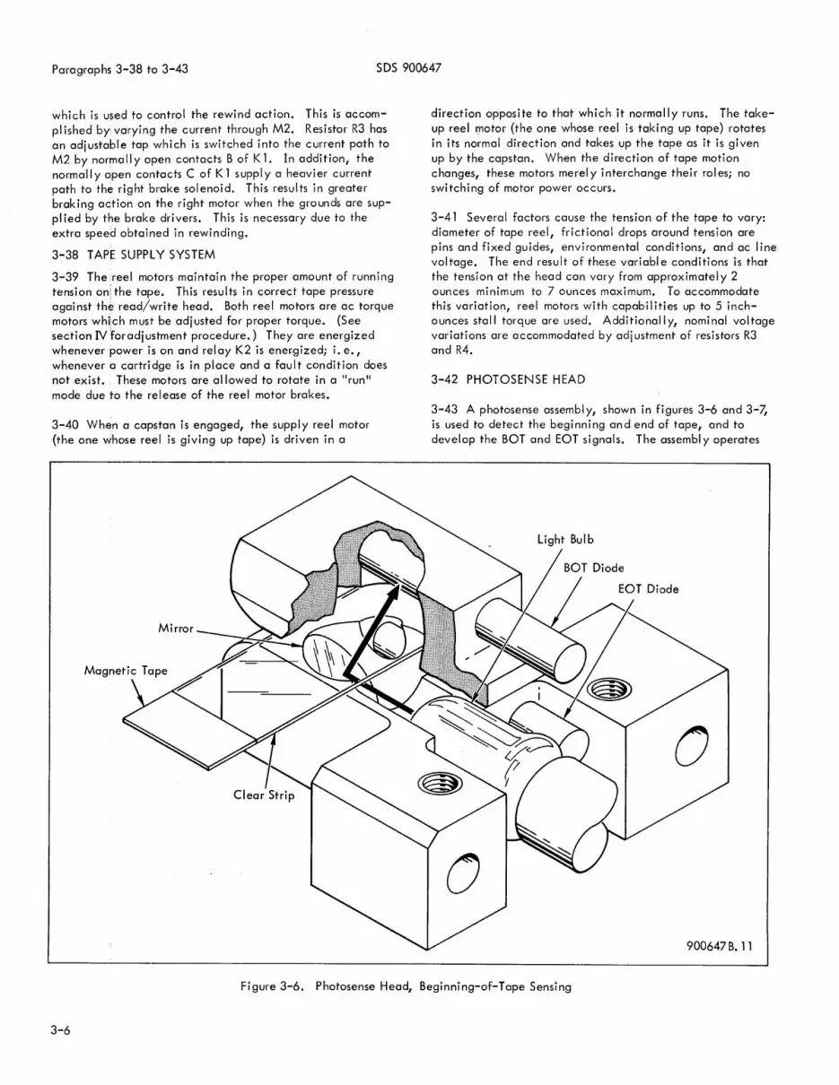
Paragraphs 3-38 to 3-43 SDS 900647
which is used to control the rewind action. This is accompi ished by varying the current through M2. Resistor R3 has an adjustable tap which is switched into the current path to M2 by normal I y open contacts B of K 1. In addition, the normally open contacts C of K 1 supply a heavier current path to the right brake solenoid. This results in greater braking action on the right motor when the grounds are suppi ied by the brake drivers. This is necessary d.ue to the extra speed obtained in rewinding.
3-38 TAPE SUPPLY SYSTEM
3-39 The reel motors maintain the proper amount of running tension on: the tape. This results in correct tape pressure against the read/write head. Both reel motors are ac torque motors which must be adjusted for proper torque. (See section IV foradjustment procedure.) They are energized whenever power is on and relay K2 is energizedi i. e., whenever a cartridge is in place and a fault condition does not exist. These motors are allowed to rotate in a "run" mode due to the release of the reel motor brakes.
3-40 When a capstan is engaged, the supply reel motor (the one whose reel is giving up tape) is driven in a
direction opposite to that which it normally runs. The takeup reel motor (the one whose reel is taking up tape) rotates in its normal direction and takes up the tape as it is given up by the capstan. When the direction of tape motion changes, these motors merel y interchange thei r rol eSi no switching of motor power occurs.
3-41 Several factors cause the tension of the tape to vary: diameter of tape reel, frictional drops around tension are pins and fixed guides, environmental conditions, and ac line voltage. The end result of these variable conditions is that the tension at the head can vary from approximately 2 ounces minimum to 7 ounces maximum. To accommodate this variation, reel motors with capabi I ities up to 5 inchounces stall torque are used. Additionally, nominal voltage variations are accommodated by adjustment of resistors R3 and R4.
3-42 PHOTOSENSE HEAD
3-43 A photosense assembly, shown in figures 3-6 and 3-7, is used to detect the beginning and end of tape, and to develop the BOT and EOT signals. The assembly operates
o
900647B.11
Figure 3-6. Photosense Head, Beginning-of-Tape Sensing
3-6

SDS 900647 Paragraphs 3-44 to 3-48
o
900647B.12
Figure 3-7. Photosense Head, End-of-Tape Sensing
by means of a light bulb (2.5-volt, 0.35-amp, TL 1-3/4, midget grooved base, C-2R filament), which provides a light source for two si I i con photoconductive diodes. The photosense assembl y is so constructed that I ight emitted from the bulb is refl ected by a mirror. When the light passes through a 1. 5-inch clear space of tape near the beginning of the reel, it projects on the upper photosense diode and develops the BOT si gnal. When the 1-inch endof-tape reflective marker passes through the photosense assembly, light is reflected back downward and projects on the lower photosense diode, developing the EaT signal. (Note that in figure 3-7 the reflective strip is shown in phantom. )
3-44 PROTECTNE CIRCUITS
3-45 Several circuits in MAGPAK help prevent damage to the equipment. These include a power interlock circuit, the tension arm limit switches, and the file protect switches.
3-46 Power Interlock Circuit
3-37 The power interlock circuit consists mainly of the Faul t Rei ay, K2, an d the Rewind Relay, K 1. These are shown in figure 3-5. All power, except the +50 volts to the brake solenoids, is routed through the normally open con" tacts of K2. Therefore, in order to operate the tape transports, the Fault Relay must be energized (i. e., no fault condition present).
3-48 Once rei ay K2 is energized, it suppl ies 117 volts Oc through contacts A directl y to the capstan motor, M 1, through R3 to the right reel motor, M2, and through R4 to the left reel motor, M3. K2 suppl ies +50 volts through its normally open contacts B to the normally closed contacts C of relay K 1. This +50 volts is fed through RC networks to the forward and reverse pressure roller solenoids, L4 and L3. K2 also supplies +25 volts via contacts C to the file protect switches and indicator lamps. This +25 volts is also supplied toone side of the rewind relay, Kl, enabiingK1 to be

Paragraphs 3-49 to 3-57 SDS 900647
energized when its driver suppl ies a ground (during rewind only).
3-49 The energizing path for K2 is through the BOR (beginning-of-reel) and EOR (end-of-reel) contacts and the RESET button. The onl y way to energize K2 is by depressing the RESET button. There is then a lock-up path through the normall y open contacts D of K2. Relay K2 cannot be energized if either the BOR or EOR contacts are open.
3-50 Tension Arm Limit Switches
3-51 The tension arm limit switches, S8 and S9, are spring action microswitches which are controlled by the tape tension arms and desi gnated BOR and EOR. The following conditions cause either one or both of these switches to open:
a. Tape reaches the beginning of the rf;lel
b. T ape reaches the end of the reel
c. A tape cartridge is being loaded (and the load handle is in the LOAD position)
d. Improper operation causes tape to bind or drag.
3-52 File Protect Switches
3-53 The file protect switches, SlO and Sl1, are snapaction, SPDT switches. When the contacts of these switches
Differentiator
Input 40
(LRD1+LRNl ) +LRD2+ LRN2
Threshold 20 Select (WRTS)
Low - Pass Filter
High Threshold
Threshold Selector
Low Threshold
-
are in the normal I y closed position (i. e., when no write plug is inserted between the switch lever and the bottom of a tape cartridge), the file protect signals, FPN and FPD, are true. When the contacts are in the normally open position (with a write plug inserted), +25 volts is supplied to the write amplifiers. Thus, the file protect switches prevent accidental writing on any tape channel which should be protected.
3-54 READ CIRCUITS
3-55 The read circuits are all contained on two circuit module cards, the HX30 Gated Read Amplifier and the HX29 Data Ampl ifier. Refer to section V of this manual for schematic diagrams of both circuits. Figure 3-8 is a block diagram of the HX29.
3-56 HX30 Gated Read Amplifier
3-57 The HX30 contains four gated differential amplifier circuits that amplify the read head signal approximately 50 times. This stage is a so-called "Iong-tailed pair, II an arrangement in whi ch the emitter resistor of the differential pair is replaced by a transistor biased to present a current source to the differential emitter terminals. This provides a high degree of common mode rejection, a very desirabl e characteristic for amplifiers receiving signals on long leads and in a high-noise environment. The outputs of the HX30 preamplifiers are gated into the HX29 Data Amplifier.
Linear Squaring Line Gain Amp Amp Driver
6 Output (RDAS)
Bias
12
Read Disable (DATA)
Threshold Detect
900647B. \3
Fi gure 3-8. HX29 Data Ampl ifier Block Diagram
3-8

SDS 900647 Paragraphs 3-58 to 3-77
3-58 HX29 Data Ampl ifier
3-59 The HX29 contains a tape signal reeld amplifier which performs peak detection and has adjustabl e threshol ds for noise rejection and ampl itude check. There are two selectable thresholds, so that one level of noise rejection can be used during a read operation and another level during a read-after-write operation. The peak detection circuit is designed to operate with a frequency modulated tape signal of 4 to 12 kc. Gain is adjustable, so thai" the amplifier will read signals from 15 millivolts to 1.0 volt.
3-60 The HX29 can be functionally divided into seven stages: filter, differentiator, linear amplifier, squaring amplifier, line driver, threshold detector, and threshold selector. Refer to figure 3-8 for the following discussion.
3-61 Filter. The read data signals from the ,HX30 pre-ampl ifiers are first input to a low-pass filter, which removes I ine noise. The input signal frequencies eire 5.5 kc and 11 kc, and the filter is designed to roll off ai' 25 kc. This rolloff point is as close to the uppermost signal frequency as possible without causing adverse signal attenuation.
3-62 Differentiator. The data si gnal output from the fi Iter is nearl y sinusoidal. The purpose of differentiating the data signal is to allow less circuitry to be used in the following stages. When the data signal is differentiated, its peaks (which correspond to flux reversals on the tape) are converted to zero crossings. It is simpler to detect and square zero crossings than an unbalanced sine wave. The output of the differentiator is a symmetri cal integrated waveform whose average dc level is zero volts.
3-63 linear Ampl ifier. The I inear amplifier is an integrated circuit differential amplifier. A gain control is provi ded to accommodate a wide range of read head signal amp I itudes. The linear ampl ifier also has a bias adjustment which can be used to balance initial dc offset and to set the output dc I evel. The output of the linear ampl ifier is fed to both the squaring ompl ifier and the threshold detector.
3-64 Squaring Ampl ifier. The squaring ampl ifier converts the data signal into square waves by ampl ifying and cI ipping. The circuit used is a differential ampl ifier with one input connected to the signal and the other input connected to the dc or quiescent lev~1 of the signal.
3-65 line Driver. The I ine driver is either cut off or driven to saturation. Its input depends upon three signals:
a. The square wave data signal from the squaring amplifier
b. The read disable signal (which is enabled when the tape unit is in motion and sel ected)
c. The output of the threshold detector.
A false signal from any of these inputs will produce a constant true output. Since the read circuits in the tape
controil unit are looking for a change in the data signal, a constant true (or false) signal is interpreted as no data or gap. Provided there are no fault conditions, the driver wi II simply follow the data input from the squaring amplifier.
3-66 Threshold Detector. The threshold detector full wave rectifies the data signals and compares the resulting dc level against a reference threshold. This dc level is an indication of the ampl itude of the read data. The threshol d detector disables the line driver if it detects a low threshold level. The reference voltage can be preset to one of two levels, which are selected by the threshold select stage.
3-67 Threshold Selector. The threshold select stage selects one of two possible threshold reference voltages. Selection is controlled by a single i,nput, WRTS. If the input is true, it selects one reference voltage; if the input is false, it sel ects the other. Both reference vol tages can be adj usted, thereby making it possible to adjust the point at which a read or write error is detected.
3-68 TAPE TRANSPORT UNIT FUNCTIONAL DESCRIPTION
3-69 The MAGPAK Tape Transport Unit performs three main functions: status/select encoding, motion control, and dato transfer. The direction of signal flow for these functions is shown in figure 3-9. Refer to this figure for the following discussion.
3-70 STATUS/SELECT
3-71 The status/select logic reports the status of a transport unit to the computer via the tape control un it. It does this in response to interrogations from the computer. The computer interrogation selects which tape unit the status is being requested upon.
3-72 MOTION CONTROL
3-73 The motion control logic stores motion commands received from the computer and transm its them to the sel ected tape transport. In the manual mode, pushbuttons on the transport control panel control the logic (and therefore the motion) of the tape transport.
3-74 DATA TRANSFER
3-75 The data transfer logic gates data from the selected tape transport to or from the computer. The direction of data flow depends on whether a read or write operation is in progress. Data is gated to the computer for reading and to the tape transport for writing.
3-76 TYPICAL PROGRAMMED SEQUENCE
3-77 In the AUTOMATIC mode, the computer program has compl ete control of tape unit operations. This is accomplished by use of magnetic tape EOM (ENERGIZE OUTPUT M) instructions. The computer monitors tape unit status
3-9

Paragraphs 3-78 to 3-82 SDS 900647
r--------------------I 9446 Tape Transport Unit
----,
rom SDS
To/F Any
900 S Com
eries puter ..... ....
9448 _ ... Tape ..
Control Unit
I I I I I I I I I I I - i .... I I I I I
""""'- : .... I I I I I
Motion ... Manual ..... Control .. Control ~
Logic
~~
" Status/Select --.. ..... Transport ... Logic ....
~~
" Data .. Transfer ...... ... ..... Logic
L _____________________ __ ...1 900647B.14
Figure 3-9. MAGPAK Functional Block Diagram
inputs for effective feedback control. A typical sequence of operations for magnetic tape is as follows: The computer alerts a buffer to select the desired tape unit; the computer then tests the status of the selected tape unit. Is it ready? Di d it receive the sel ect signal? Is it at the beginning or end of tape? Is the selected channel fi Ie protected? The comp uter can test any or a II of these status i ndi cators. Depending upon the results of the status tests, the computer then outputs an operation command. These operation commands, such as read, write, scan, etc., are converted to motion commands in the tape control unit. The tape transport unit then receives one of four motion commands:
a. Start Forward
b. Start Reverse
c. Rewind
d. Stop
3-78 After the motion control logic in the tape transport unit sets the mechanics of the tape unit into motion, data is channeled to or from the selected tape read or write head. This data is either presented to or taken from the tape control unit. In general, this operation continues until the
. computer transmits a different command. During rewind,
3-10
however, if the beginning of tape is reached, a stop signal !s generated by the logic in the tape unit itself.
3-79 TAPE TRANSPORT UNIT LOGIC DESCRIPTION
3-80 INTRODUCTIOt"
3-81 A basic knowledge of the logic used in SDS computers is essential to the understanding of logical functions performed by MAGPAK. For purposes of discussion and brevity, many logic equations in the following paragraphs show only part of their gate mechanizations. A compl ete I isting of tape transport unit logic equations and a glossary of logic terms are included at the end of this section. Logic diagrams, showing connector and pin locations of signals, are included in section V of this manual.
3-82 Figure 3-10 is a simpl ified logi c diagram showing the three main logical functions of the tape transport unit: status/select, motion control, and data transfer. It also shows the interface between the tape control un it, the tape transport unit electronics, and the transport/control panel assembly. The tape unit shown in figure 3-10 is transport No.1; the logic for transport No. 2 is the same except that signals are labeled differentl y. For example, TSAl refers to station No.1, and TSAl. refers to station No.2. Certain circuits such as the read ampl ifier and the CHSB flip-flop, however, are common to both transport units.

9448 TAPE CONTROL
UNIT
Status Signals
TfPS
!.Mit SeI8Ct{LLTO lines I
Dil'llCtlyto : Units I &2 LLT7
Start T12S Forward
Start SI2T Reverse
Rewind
Stop STOP
Write Data WDAS
WDAS
Write WRTS Contll)l
STATUS/SELECT LOGIC
LTDl
FPNI
LTNI
FPDI
9446 TAPE TRANSPORT UNIT (ELECTRONICS)
EOTl ----to St-----t
EOTl flip-Flop
1J---~
~ 0.1 msec
AUTl
MAN 1
BOT
BTl
BOT
EOT
Ell 1
Unit Select lines --------------.-,----------------------_._---------
TSBI
MOTION CONTROL LOGIC
TSAI
TS81
AUTI
TS81
TSAI
SELS
Read Data RDAS
DATA TRANSFER LOGIC
MAN 1 TS81
EOll
BOll REWM
RDYI
T12S
SI2T
ROYI
ROY 1
REWM
CHSB
CHSB
S 0
TSAI lip-Flop
R 1
R 0
TSBI Flip-Flop
S 1
DATA
WRTS
Amplifier
TSAI
TS81
TSBI
TSAI
Even 2 Odd 2
CHSB
SEll
Manual Control Buttons are Connected to TSA I and TSBI Outputs via Diode Logic
CHSB WRTS
SELl
CHSB
WRTS
CHSB ----.... ..,
FWDI
REVI
REWI
BRKI
{ ------t
-WENI
_WEDI
WEN!
Preamplifiers
{
SDS 900647
9446 TAPE TRANSPORT UNIT (MECHANISM/CONTROL PANEL)
MANUAL
ODD EVEN LLTO ~~ ~~
I ~ I I I I -0
LLT7 -o~ -o~
UNIT SELECT SWITCHES
Forward Pressure Roller
Reverse Pressure Roller
Rewind Relay K I
Brake Solenoids
Manual Pushbuttons
K2 SffiP If Fault
.....CI- Forward t----oo 0
I--------<l~ Reverse \ Grolnd
.. If In Manual --C- Rewind 7
I-----------~ 0
To AUT I line
C Write Head Even
C W rite Head Odd
File Protect Switches (Shown in Not PlI)tect Position)
C Read Head Even
C Read Head Odd
Figure 3-10 •. MAGPAK Simplified logic Diagram
900647B.15
3-11/3-12

SDS 900647 Paragraphs 3-83 to 3-95
3-83 STATUS/SELECT LOGIC
3-84 Unit Select Lines
3-85 Operation of a tape station is initiated when the proper address is selected on the incoming unit select lines (LLTO to LLT7). These lines are routed through Cable Plug Module P84 to all tape stations in the system. The unit select lines are connected to the UNIT SELECT switches on the transport control panel. An active unit select I ine will be grounded. The active I ine is determined by the setting of the UNIT S ELECT switch. The ground is sent back to the status/select ..!?gic as either LTDl or LTN 1 (fo~e station No.1). LTDl refers to the odd channel and LTN 1 to the even channel.
3-86 The first status signal that must be sent back to the tape control unit is the select acknowledge (AANS) signal. This signal is at ground when it represen·ts an acknowledge condition.
AANS = LTDl + LTN 1 + LTD2 + LTN2
The above e~tion is derived in the following manner. LTNl and LTDl are ANDled together ar:!~ut to an inverter. Therefore, if either L TN 1 or LT D 1 are at ground (indicating that the odd or even channel of tape station No. 1 has been selected), the output of this inverter will be true. This true output enables the common input of all the status inverters. Since the inverter used to develop AANS has a constant true input, the output will be pulled to ground when its common input swings true. An identical inverter for tape station No.2 is OR led into the AANS I ine. This inverter wi II produce a ground if either LTN2 or L T D2 is se I ected.
3-87 Ready
3-88 The tape station is ready provided it is in the automatic mode, no motion is in process, and no fault condition exists. A fault condition occurs when tape comes to the physical end or beginning, or a cartridge is unloaded. When the fault condition is cleared and the RESET pushbutton is depressed, the AUTO signal goes true and the unit is again ready.
RDY = (LTN + LTD) AUT FWD REV REW
where:
AUT = K2D AUTO SWITCH
sK2 = BOR EOR RESET BUTTON
3-89 Logic is also provided to assure that if the beginningof-tape point is being approached, the ready signal will be inhibited until tape motion has stopped. This is necessary to ensure thClt the load point is always sj'arted close to the
same point. The logic consists of the beginning-of-tape signal, BOT, and a delayed beginning-of-tape signal, BTS, ANDled together to drive an inverter. This inverter will inhibit the development of the ready signal when its output is false.
3-90 When a tape unit is not at the beginning-of-tape point, a capacitor on Cable Plug Module P84 discharges to ground and suppl ies a false input to an inverter; this, in turn, arms one I eg of an AN D gate. The other leg of this AN D gate is at ground because the BOT signal is false. This makes the output of an inverter fed by this AND gate true. Therefore, the ready signal is not inhibited at that time.
3-91 When a tape unit reaches the beginning-of-tape point, the BOT signal goes true and the capacitor on P84 starts to charge. For the duration of the charge time, the inverter it drives is still hel d true. During this time, the AN D gate has both inputs true and thus the inverter it drives is held false. This inhibits the ready signal until the capacitor charges to a level sufficient to switch the inverter it drives. The time required to charge the capacitor to this level is approximately 100 milliseconds, which is ample time for tape motion to come to a stop.
3-92 End-of-Tape
3-93 End-of-tape status is indicated by the end-of-tape flip-flop being set. This occurs when the tape unit has been going in a forward direction and the end-of-tape reflective marker has been encountered. The end-of-tape fl ip-flop is reset when tape is moving in the reverse direction and the end-of-tape marker is sensed. The end-of-tape fl ip-flop is also reset any time there is a fault condition.
sEOT (ETTl TSB 1) SBOTl
rEQT K2 + ETT 1 TSB 1 + - - -
where:
ETTl EOT
TSBl FWDl
TSBl REVl + REWl
SBOTl BOT
3-94 Beginning-of-Tape
3-95 The beginning-of-tape signal (BOT) is present when the tape station is positioned such that the beginning-oftape clear space is stationed at the photosense head. As shown in figure 3-10, BOTl is generated in the same manner as the ready inhibit circuitry. BOll is used in a reset function of the motion control logic. When BOT is approached, the true pulse caused by the delay of BOll wi" reset the TSA and TSB fl ip-flops.
3-13
Paragraphs 3-96 to 3-108 SDS 900647
3-96 File Protect
3-97 The file protect signal is true if there is no write plug inserted for the channel that is being tested. For example, if the write pi ug is missing on the odd channel of one of the tape stations, and that channel is interrogated for fi Ie protect, the response will be file protected. A similar response is involved when checking for the even channel.
TFPS = FPN1 LTDl + FPDl LTNl
+ FPN2 LTD2 + FPD2 LTN2
In the above equation, signals FPDl and FPN 1 are true when the file protect switches are closed for the odd and even channels {respectively} of tape station No. 1. Similarly, FPD2 and FPN2 are true when the odd or~n channels of tape station No.2 are file protected. LTD1, LTN 1, L TD2, and LTN2 are generated when the odd' or even tracks of either tape station have been selected.
3-98 If both the file protect switches for a particular transport are in the non-protect position, the output of the TFPS inverter is true. This is because both input AN D gates are disabled by false inputs on FPD and FPN. As in all status I ines, both transports have identical logic OR led into one line.
3-99 The file protect switches also create write enable signals, WED1, WEN 1, WED2, and WEN2. These signals are used to enable the write amplifiers for their respective tape channels. For example, WENl will supply an enabl ing voltage to the write ampl ifier for the even track of tape station No. 1 when the file protect switch for that track is not in the protect position.
3- 100 I ndi cators
3-101 The indicator lamps on the tape transport unit control panel are turned on by the following signals:
LOAD POINT {BRL}
READY (RDL)
EN D OF TAPE {ETL}
BOT
RDY
EOT
FILE PROTECT ODD FPD
FILE PROTECT EVEN FPN
These indicators are driven by an IK51 Inverter Ampl ifier. When a transport unit is in operation and the indicator is OFF, a small current is present in the indicator. This reduces the initial start current of the bulb to a level that can be handled by the driver. The bulbs are always prewarmed before use since all bulbs are in the OFF state during a power-on sequence.
3-102 MOTION CONTROL LOGIC
3-103 The basic motion of the tape transport unit is controlled by the TSA and TSB flip-flops. When both flip-flops
3-14
are reset, the transport is stopped. When TSA is set, the transport is going forward; with TSB set, the transport runs in reverse. With both TSA and TSB set, the unit is rewinding.
No Motion TSA TSB
FWD TSA TSB
REV TSA TSB
REW TSA TSB
3-104 The TSA and TSB flip-flops are set and reset by signals from either the tape control un it or push buttons on the transport control panel in conjunction with status signals {i. e., beginning-of-tape, end-of-tape, ready, etc.} from the transport. All operations are completely interlocked so that no sequenc ing of any control panel buttons or commands from the tape control unit wi II cause tape damage. The fault relay, K2, prevents erroneous tape operation during a power-on sequence. Also, K2 disconnects power from the unit if a fault occurs while the transport is operating; no further operations are possible until the operator intervenes.
3-105 Manual Control
3-106 The tape station can be run from the control panel with the AUTO-MANUAL switch in the MANUAL position, providing a tape cartridge is in place and the RESET pushbutton has been pressed. In order for the tape station to reset, the end-of-reel and beginning-of-reel switches must be closed.
----sK2 = BaR EaR RESET Button
If the beginning-of-reel or end-of-reel switches open after operation has commenced, the transport wi II become disabled after approximately 100 milliseconds.
rK2 = BaR + EaR
The time delay is inserted to prevent spurious signals from causing a fault condition {e. g., a tape tension arm momentarily opening the BaR or EaR switch}.
3-107 In the manual mode of operation, the tape station will not respond to any commands from the tape control unit. This is because the set input gates of the TSA and TSB fl ipflops are inhibited by the ready signal. RDY is held false by AUT, which is at ground when the unit is in the manual mode. The control panel pushbuttons directl y set or reset the appropriate flip-flops by directly grounding the true or false outputs.
3-108 A diode network located on Cable Plug Module P82 is used to select the true or false side of the TSA and TSB flip-flops. These diodes decode which flip-flops are to be set or reset from each control panel button. For example, if the FORWARD button is pushed, a ground is applied to the false output of TSA and the true output of TSB. TSA is

SDS 900647 Paragraphs 3-109 to 3-119
then forced to set and TSB to reset. This is decoded to produce an enable signal to the forward pressure roller. The decoding logic for the three motion functions can be expressed:
FWD1 = TSA 1 TSB 1
REV1 = TSA1 TSB1
REW1 = TSA 1 TSB 1
The brake solenoids are activated if nonE~ of the above equations are satisfied:
BRK 1 = FWDl REV 1 REWl
This decoding logi c is used in both manual and automatic modes.
3-109 The reset function of BOT is also common to both modes. BOT will reset both motion fl ip-flops when the beginning-oF-tape (load point) is approached:
rTSA 1 BOT 1 BOTl + - - -
rTSB 1 BOT 1 BOn + - - -
BOT 1 is true when beginning-of-tape is sensed; BOT 1 is true when the unit is not at the beginning-of-tape and when BOT 1 has i ust been sensed. This logi c sf'ops the transport at load point no matter what motion is in progress. In manual, any motion can be reinitiated from load point.
3-110 If the transport is in manual and moving forward, it wi II stop when the end-of-tape marker is encountered:
rTSAl = MAN1 (TSBl EOTl + - - -) + - - -
In this equation, TSB 1 is reset for forward motion and EOTl is the end-of-tape signal. After the end-of-tape marker is sensed in the forward direction, onl y reverse or rewind operation is possible because TSA is held reset by EOTL
3-111 Automatic Control
3-112 The basic operation of forward and reverse motion in automatic is the same as in manual; the only difference is in the method of setting and resetting the parti cular fl ipflops. In order for either TSA or TSB to be set, the tape station must be in the automatic mode, ctddressed, and there must be no rewind stop delay in process:
where:
sTSA 1 = RDYl (BOTl REWM + Tl2S) + - - -
sTSB 1 = BOn RDY1 (REWM + S 12T) + - - -
RDYl = AUT (LTNl + LTD1) BOn = Not in load point delay time S 12T = Start'reverse T 12S = Start forward REWM= Rewind
3-113 There are four commands from the tape control unit that are recogn ized by the tape station when it is addressed and in automati c. These commands are: start forward (T 12S), start reverse (S 12T), stop (STOP), and rewind (REWM). Forward, reverse, and rewind are the only commands that will set the motion fl ip-flops. The start forward command sets TSA; the start reverse command sets TSB. Rewind sets both TSA and TSB, and stop resets both TSA and TSB. The tape station wi II ignore rewind and reverse commands if it is ot load point. BOTl disabl es all input set gates except the forward gate:
sTSAl = RDY1 Tl2S + - - -
3-114 Both forward and reverse motions can be stopped at any time:
rTSA 1 = TSB 1 SEL 1 STOP (stop forward) + - - -
rTSB 1 = TSA 1 SEL 1 STOP (stop reverse) + - - -
where:
SEll AUTl (TSAl TSBl + TSAl TSB1) + - - -
A rewind operation, however, can not be stopped with the stop command. This is because in rewind both fl ip-flops are set; in order for ei ther fI ip-flop to reset, the opposite fl ipflop must already be in a reset condition.
3-115 DATA TRANSFER LOGIC
3-116 Data can be read or written on either the odd or even channel of any tape station. Selection of the odd or even channel for a particular tape station is accomplished at the time of command. If the ~ channel has been selected, the CHSB fl ip-flop wi II be set:
sCHSB = (LTN1 + LTN2) (Tl2S + S12T)
Selection of an odd channel resets CHSB:
rCHSB = (LTDl + LTD2) (T12S + S12T)
3-117 Selection takes place when the tope unit is in automatic and any motion is in process except rewinding:
SELl = AUTl(TSA1TSB1+TSA1TSB1)+---
The sel ect line (SELS) goes active back to the control unit to indi cote that data is, or should be, transferred to or from a transport unit. Once a unit is selected, de-selection does not take place unti I after the stop pulse goes false (approximately 10 msec after STOP goes true):
SEll = STOP AUTl SEll + - - -
3-118 Reading
3-119 A preamplifier/postampl ifier system is used to retrieve the digital data written. {The theory of operation of these
3-J5

Paragraphs 3-120 to 3-134 SDS 900647
circuits is covered under "Read Circuits. ") There are four preamp I ifiers on one HX30 Gated Read Ampl ifier circuit module. Each tape read head feeds one of these preampl ifiers. The particular preampl ifier to be activated is selected by the select signals and the output of the channel
. select flip-flop:
SEll C HSB + SEll C HSB + SEL2 CHSB + SEL2 CHSB
The select signals also activate the postamplifier:
DATA = SELl + SEL2
These seled si gnals allow the read ampl ifier to operate onl y when the transport is in motion:
SEll = AUT1(TSA1TSB1+TSA1TSB1)+---
The outputs of the HX30 preampl ifiers are OR led into the input of the HX29 postamplifier.
3-120 A write select signal (WRTS) from the tape control unit is used in the postamplifier to select the threshold. During normal read operations, WRTS is false, causing a low threshold in the amplifier. During write operations, a read-after-write check is performed. WRTS is then true and a high threshold is selected. This makes the read-afterwrite check more sensitive to the detection of write errors.
3-121 Writing
3-122 Write selection is similar to read selection, but is further qual ified. First, there must be a write pi ug in the tape cartridge corresponding to the channel to be written. Second, the write select line (WRTS) must be active from the tape control unit. For example, writing on the odd channel of tape station No. 1 is selected by:
SEL 1 CHSB WRTS WEDl
In this expression WEDl supplies collector voltage to the odd channel write amplifier provided the file protect odd switch is closed. WEN 1 performs the same function for the even channel write amplifier. Write selection also activates the associated read selection, thus allowing a readafter-write check at the tape control unit.
3-123 Writing is controlled by the tape control unit. Information is written on the tape in a saturation mode. The data that is placed on the tape is dependent upon the two write lines (WDAS and WDAS) from the tape control unit.
3-124 TAPE CONTROL UNIT FUNCTIONAL DESCRIPTION
3-125 The 9448 MAGPAK Tape Control Unit can be divided into four functional sections as indicated in figure 3-11. The heavy lines in figure 3-11 distinguish information flow from control signal paths. The control logic section interprets EOM commands and addresses. This
3-l6
section coordinates the tape motion command sequences with the information transfers into and out of the computer. The Harvey register section has as its primary functions the conversion of parallel computer output signals to serial for writing and serial playback signals to character parallel in reading. The Harvey register also operates in a counting mode to provide timing signals to the control logic. The write logic section encodes the serial signals into frequencydoubling bit format. The dc erase signals are also generated in the write logic. The read logic section decodes the frequency-doubling bit format, maintains bit synchronism on the playback signal, and detects gap. Additional I y, the read logic detects the preamble, checks character parity on the playback information, and signals the end of a record as the postamble is detected.
3-126 WRITE LOGIC SECTION
3-127 Figure 3-12 shows the write logic section separated into functional groupings of flip-flops. The reference clock, FC, is the precision source of timing pulses for writing. The FC signal runs at 12 times the bit transfer rate or 126 kc. This signal is used throughout the MAGPAK Tape Control Unit as a flip-flop clocking term.
3-128 Write Clock Generator
3-129 Under the control of gates generated in the control logic section, the write clock generator flip-flops (WCAWCD) divide the reference clock frequency by 12, producing two symmetrically out-of-phase write clocks, WCPO and WCPl. Information shifting in the Harvey register is strobed into the write flip-flop, WF, by WCPO causing the write signal, WDAS, to make a transition for each logical zero. The WCPl pulse always toggles WF to its opposite state, producing the synchronizing transition in each recorded bit.
3-130 Write Synchronizer
3-131 The write synchronizer (WSA-WSC) counts the WCPO pulses. Every seventh pulse, the write character gate, WGO 1, is generated. The control logic uses the WGO 1 gate to initiate the output of a character from the computer during writing operations.
3-132 The write logi c section is enabled by the control logic whenever the computer buffer is addressing MAGPAK. Thus, the WGOl pulses are available for timing certain MAGPAK operations. These pulses, which occur at a 1.5-kc rate, are counted in the Harvey register to provide delays and intervals in the starting and stopping sequences. Also, the control logic uses WGO 1 as a standard time for state changes.
3-133 READ LOGIC SECTION
3-134 Fi gure 3-13 shows the read logic section separated into functional groupings of flip-flops. The reference clock, FC, is the same precision source of timing pulses that is used for writing.

SDS 900647
I Control Strobes
I Address lines Motion Control I : Input Control Transport Address I
I Output Control Control I Logic Ready, File Protect, Select
I Ready, File Protect Section Read/Write Track Sel ect !. ! Error
I Write Control I : External Clock I
I t
I I FM encoded I I Timing Delay information to I 9446
COMPUTER I Gates Write head. Also I MAGPAK Write ERASE signal. Input/Ou tput I Logic Tape
Channel I· Transport
I Read/Write Section I Control
Unit
I l I I •• I I I I I
... 1 ... I -., 6 Bits + Parity
Harvey 6 Bits + Parity FM encoded I I Parallel Information
Register Serial Information information I
I Section - from Read I Synchron iz ing Gates Read Preamp I ifier
I Logic I
-- I
I Sh ift Control Gates Section I
I I L ________________________ J
900647B.16
Figure 3-11. Tape Control Unit Block Diagram
Harvey Register Output HROO
,f ~ tJ "\ f ~,,"l Reference Clock FC Write
\tiffJj ~ Flip-Flop
Write Clock Generator Write Clock WCP1 .. Write Signal WDAS ...
ntrol Co G ~
WCA
(6)
WCB WCC
(22) (21
)
- .... WF .. .... ....
WCD Write Clock WCPO
(2°) Write Synchronizer
Write Charact er
WSA WSB WSC Gate WGOl .. ... .... (22) (2
1 ) (2°)
.. 900647B.17
Figure 3-12. Write Logi c Section Block Diagram
3-17
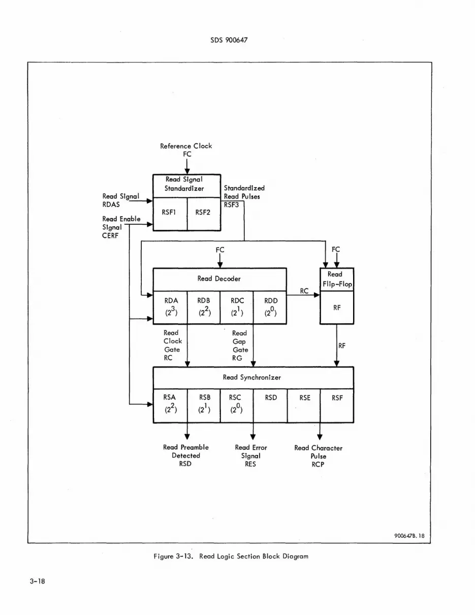
3-18
Read S RDAS
Read E Signal CERF
tgnal ... .. nable ... ..
4
... ...
... ..
SDS 900647
Reference Clock FC
~ Read Signal Standardlzer
RSFl RSF2
Standardized Read Pulses RSF3
r Read Decoder
RDA RDB
(23) (22)
Read Clock Gate RC
~r
RSA RSB
(22) (21 )
" Read Preamble
Detected RSD
RDC RDD
(21 ) (2°)
Read Gap Gate RG
~,
Read Synchronizer
RSC RSD
(2°)
~,
Read Error Signal
RES
~. Fl
Read Flip-Flop
RC ... .. RF
RF
~.
RSE RSF
" Read Character Pulse RCP
Figure 3-13. Read Logic Section Block Diagram
900647B.18

SDS 900647 Paragraphs 3-135 to 3-150
3-135 Read Signal Standardizer
3-136 In the read signal standardizer, Fe is used to clock the read signal, RDAS, into RSF 1 and then into RSF2. The outputs of these fl ip-flops are delayed versions of the RDAS square wave. By gating RSF 1 with RSF2, a set of read pulses, RSF3, are generated which provide a quantized representation of the zero-crossings in the RDAS.
3-137 Read Decoder
3-138 The read decoder, RDA-RDD, operates as a variable period binary counter clocked by FC and synchronized by RSF3 pulses. The counter is uncaged by an RSF3 pulse and starts counti ng upward from zero. The contents of the count~r defin'e the time intervals shown in figure 3-2. A gap condition wi II be recognized in the read decoder which stalls and waits for another zero-crossing. As preamble ones arrive, i'he counter receives only synchronizing transitions on RSF3 for 8 bit times.
3-139 Thus, the counter receives RSF3 pulses during the sync confirm time interval onl y. If a transition occurs within the zero detect time interval, the read decoder indicates the arrival of a zero but does not reset. Once the read decoder establishes synchronism,. only the RSF3 pulses that arrive within the sync confirm time interval will reset the counter.
3-140 As the read decoder cycles, the read clock, RC, is generated for each bit time. The read g(lP signal, RG, is suppl ied whenever a spurious transition is detected during the first third of a bit time, or when no transition is detected unti I after the read decoder has counted to a state representing 1-1/3t bit time.
3-141 Read Flip-Flop
3-142 The read fl ip-fl op, RF, is used to convert the frequency-modulated si gnal to binary. This conversion is accompl ished by arming RF at each read clock, RC , and resetting RF to zero on any RSF3 that occurs within the zero decode time interval as defined by the read decoder. The content of RF is strobed by RC in subsequent logi c.
3-143 Read Synchronizer
3-144 The Read Synchronizer, RSA-RSF I performs six functions:
a. The preamble code is detected. The arrival of the preamble zero establ ishes the read synchronozer in synchronism with the characters of the record.
b. Character synchronism is maintained within the read synchronizer by counting in 7-bit cycles through the record.
c. Serial odd-parity errors are detected.
d. If a read gap signal, RG, occurs during character processing, the read synchronizer indicates an error.
e. The first seven bits of the postable are detected and character processing is terminated.
f. The postable is confirmed when the read synchronizer is reset by a read gap signal, RG, prior to the arrival of another character.
3-145 The read synchronizer is clocked by the read clock, RC, and performs its functions by interpreting the read flipflop, RF, and read gap, RG. Once it is enabled by the control logi c, the read synchronizer functions autonomousl y during write as well,as read operations.
3-146 It is desirable to consider the read synchronizer flipflops to be divided according to function as follows: RSARSC act as a seven-state binary counter; RSD detects the preamble; RSE is the parity error detect flip-flop; and RSF detects the postabl e.
3-147 The primary outputs of the read synchronizer are the read character pulse, RCP, which indicates the arrival of the seventh bit in each character, the read error signal, RES, and the read preamble detect, RSD.
3-148 HARVEY REGISTER SECTION
3-149 Figure 3-14 shows the Harvey register flip-flops, HROO-HR06. This general-purpose register performs four functions:
a. Acting as a shift register, the Harvey register converts the character parall el signals from the computer buffer into serial for recording. Likewise, during reading, the serial information is converted to character parallel for inputting to the computer buffer. In order to accommodate reverse scan, the Harvey register is capable of reverse shifting.
b. The indicated parallel transfers described above are mechanized in the Harvey register section.
c. During reading or scanning, the file mark is detected within the Harvey register. Additionally, in order to maintain program compatibi I ity with conventional magnetic tape, it is necessary to record file marks as two characters even though the computer outputs only one. This function is performed in the Harvey register.
d. The timing of all starting, stopping, and continue sequence is performed by the H,arvey register. Inasmuch as no information-transfers take place when this function is required, the Harvey register is converted to a binary counter from which seven time intervals are decoded.
3-150 The read flip-flop signal, RF, is supplied to the Harvey register along with the read clock, RC, during reading and scanning operations. For read and scan forward, bits from RF shift into HR06 and then through the register, clocked by RC to HROO. The computer buffer is clocked by the control logic at the read character pulse (RCP) time,
3-19

Paragraphs 3-151 to 3-156 SDS 900647
Buffer Output Signals from Computer
A r R6 R5 R4 R3 R2 R1 '\
Serial Signal from Read logic RF
Harvey Register Serio I Signa I to t---...... Write logic HROO Read Clock RC
Write Clock WCPO HR06 HR05 HR04 HR03 HR02 HR01 HROO
Write Character WGOI (2
6) (25) (24) (2
3) (22) (2
1 ) (20) STGD
Control logic WTRD
Terms SPGD Delay
SPTD Signals
CUWD
Bu ffer Input Signa Is to Computer IHGD
CURD
900647B.19
Figure 3-14. Harvey Register Block Diagram
after which the HROO-HR06 contents are transferred in parallel. For scan reverse, the sequence is the same except the bits shift from RF into HROO first, and then backwards through the register to HR06.
3-151 During writing, the computer buffer is clocked by the control logic at the write character WGO 1 time after which the HROO-HR06 are loaded in parallel. Under the control of the write clock, WCPO, the Harvey register shifts forward from HR06 to HROO. The output of HROO is the serial ized character processed by the write fl ip-flop, WF. Since it m\Jy be necessary to repeat the character to duplicate the dual fi Ie mark, the Harvey register is arranged to recirculate its contents during shifting. If the output is on I y one character, therefore, it is recorded twi ce on the tape. This action is defeated if the output is more than one character in any record.
3-152 The Harvey register is used as a binary counter under conditions defined by the control logi c. The write character pulses, WGO 1, are used as a precise 1.5-kc clock for this function. The time intervals defined by recognition of Harvey register states may be summarized as follows:
STGD ~tarl Qap .Qelay (36.p ms)
WTRD ~rite 10 Eead Qelay (34. i~s)
SPGD ~tof gap [2elay (26.0 ms)
SPTD ~toe rape Qelay (30.7 ms)
CUWD ~ontin~e yY'rite Qelay (60.7 ms)
CURD ~ontin~e Jiead .Qelay (75.5 ms)
IHGD Intert!,ead Quard Qelay (50.7 ms)
3-20
3-153 CONTROL LOGIC SECTION
3-154 Figure 3-15 shows the control logic section partitioned according to functional groups of flip-flops and gating. In addition to the control elements listed below, the tape control unit has other control circuitry which performs the following functions:
a. Forwards computer commands and addresses to the tape transport un i t
b. Interprets computer EOM instructions
c. Responds to SKS instructions
d. Allows a conventional magneti c tape system (such as SDS Model 9248) to be pi ugged into the Model 9448 auxil iary connector so that it operates compatibly over the same computer buffer channel.
3-155 Control State Counter
3-156 The coordination of all control functions of the tape control unit is provided by the control state counter, CSA-CSC. Operating in conjunction with other control fl ip-flops and control I ines from the computer buffer (in particular, WO, W5, W6, W9, W10, W11), the control state counter decl ares what MAGPAK is doi ng at every instant in time. Table 3-1 summarizes the eight control states defined by the CSA-CSC fl ip-flops.

SDS 900647
External Reverse Monitor Clock Flip-Flop Flip-Flop
CECF C12M
(de)
d.
" " Skip Remainder Control State Counter Erase Tape
Flip-Flop Flip-Flop
CSRF +-
CSA CSB CSC r--+ CETF
(de) (22) (21 ) (2°) (de)
H a ~~
'r ,~ " Continue File Mark Enable Read Flip-Flop Flip-Flop Flip-Flop
CUFF CFMF CERF
(de) (de) (de)
900647B.20
Figure 3-15. Control Logic Block Diagram
3-21

Paragraphs 3-157 to 3-170 SDS 900647
Table 3-1. CSA-CSC Control States
Control State Defined As Name
----CSO CSA CSB CSC IDLE-START
--CS1 CSA CSB CSC PREAMBLE
- --CS2 CSA CSB CSC WRITE
--CS3 CSA CSB CSC POSTAMBLE
---CS4 CSA CSB CSC INTERHEAD
-CS5 CSA CSB CSC GAP
--CS6 CSA CSB CSC STOP-HALT
CS7 CSA CSB CSC READ
3-157 External Clock Flip-Flop
3-158 The external clock flip-flop, CECF, is named for its basic function of clocking the computer buffer during information transfers. It actuall y performs four functions:
a. CECF clocks the computer buffer during write (CS2) in response to WGO 1 and in read (CS7) in response to RCP.
b. During CSO, C ECF initiates Harvey register tim-ing operations in response to various MAGPAK commands.
c. During CS 1 and CS3, C ECF is used to time the writing of the preamble and postamble codes.
d. At the beginning of CS4, CS5, and CS6, CECF clears the Harvey register in preparation for binary counting.
3-159 Reverse Monitor Flip-Flop
3-160 The remaining six fI ip-flops in the control logi c section are all of the dc-type (FH19). The reverse monitor fl ip-flop, C 12M, simpl y remembers the direction in which the tape is commanded to move. It participates in determining the control state sequence.
3-161 Erase Tape Flip-Flop
3-162 The erase tape fl ip-fl op, C ElF, is turned on at the beginning of all write or erase operations in CSO. The dc erase signal is supplied by the write logic whenever CETF is on. In write operations, CETF is turned off to start the preamble in CS 1 and back on again in CS3 to terminate the postamble.
3-22
Basic Control Activities
Idle--Ready, Forwarrl start motion commands. Erase start gap. Gate out Read
Wri te Preamble
Write characters, output from Computer Buffer
Write Postamble
Erase gap. Wait for gap to be read
Erase gap. Indi cate gap to computer
Stop tape motion. Erase stop gap. Halt Buffer
Read characters, input to Computer Buffer
3-163 Enable Read Flip-Flop
3-164 The enable read flip-flop, CERF, controls the functioning of the read logic. It is turned on when writing begins in CS 1 and when reading is to occur in CS7. Reading is disabled by turning off CERF whenever a gap is detected after the preamble has been recognized.
3-165 File Mark Flip-Flop
3-166 The file mark flip-flop, CFMF, is set at the beginning of every read operation and is reset whenever the character in the Harvey register is not a file mark. Thus, if CFMF remains set after a read, a file mark is indicated to the computer. Furthermore, CFMF acts in conjunction with CUFF and CSRF to control the duplicate writing of file marks.
3-l67 Continue Flip-Flop
3-168 The continue fl ip-flop, CUFF, stores the information that a command to continue was given in CS5. This permits CUFF to alter the state sequence so that the tape is not halted. An additional function is performed by CUFF during CS2, the writing state, in that if more than one character is to be written in a record, CUFF detects this and prevents character dupl i cat ion.
3-169 Skip Remainder Flip-Flop
3-170 The skip remai nder fl ip-flop, CSRF, is used to store the programmed command to ignore remaining characters being read. CSRF then inhibits the clocking of the computer buffer. As mentioned above, CSRF parti cipates in the writing of a file mark in duplicate. A third function
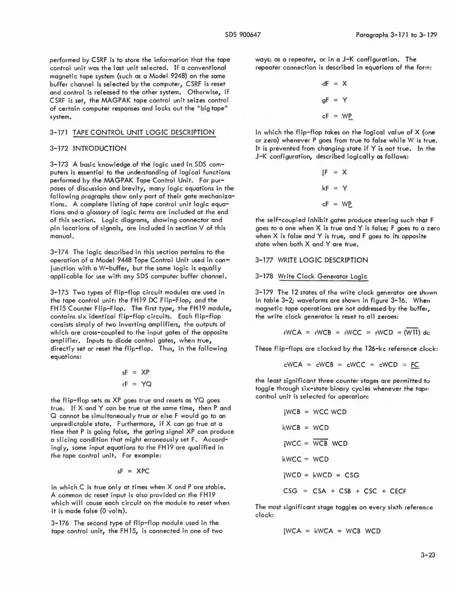
SDS 900647 Paragraphs 3-171 to 3- 179
performed by CSRF is to store the information that the tape control unit was the I ast unit sel ected. If a conventional magnetic tClpe system (such as a Model 9248) on the same buffer channel is selected by the computer, CSRF is reset and control is rei eased to the other system. Otherwise, if CSRF is setv the MAGPAK tape control unit seizes control of certain computer responses and locks out the "big tape II system.
3-171 TAPE CONTROL UNIT LOGIC DESCRIPTION
3-172 INTRODUCTION
3-173 A basic knowledge of the logic used in SDS computers is essential to the understanding of logi cal functions performed by the MAGPAK Tape Control Unit. For purposes of discussion and brevity, many logic equations in the following pragraphs show only part of their gate mechanizations. A complete I isting of tape control unit logic equations and a glossary of logic terms are incl uded at the end of this section. Logic diagrams, showing connector and pin locations of signals, are inc! uded in section V of this manual.
3-174 The logic described in this section pertains to the operation of a Model 9448 Tape Control Unit used in conjunction with a W-buffer, but the same logic is equally applicable for use with any SDS computer buffer channel.
3-175 Two types of flip-flop circuit modules are used in the tape control unit: the FH19 DC Flip-Flop, and the FH15 Counter Flip-Flop. The first type, the FH19 module, contains six identical fl ip-flop circuits. Each fl ip-flop cons ists simpl y of two inverting ampl ifiers, the outputs of which are cross-coupled to the input gates of the opposite ampl ifier. Inputs to diode control gates, when true, directl y set or reset the fl ip-flop. Thus, in the following equations:
sF XP
rF YQ
the fl ip-flop sets as XP goes true and resets as YQ goes true. If X and Y can be true at the same time, then P and Q cannot be simultaneously true or else F would go to an unpredictable state. Furthermore, if X can go true at a time that P is going false, the gating signal XP can produce a sl icing condition that might erroneousl y set F. Accordingl y, some input equations to the FH 19 are qual ified in the tape control unit. For example:
sF = XPC
in which C is true only at times when X and P are stable. A common dc reset input is also provided on the FH19 which will cause each circuit on the module to reset when it is made false (0 volts).
3-176 The second type of flip-flop module used in the tape control unit, the FH 15, is connected in one of two
ways: as a repeater, or in a J-K configuration. The repeater connection is described in equations of the form:
dF X
gF Y
cF WE.
in which the fl ip-flop takes on the logi cal val ue of X (one or zero) whenever P goes from true to false while W is true. It is prevented from changing state if Y is not true. In the J-K confi guration, described logi call y as follows:
jF X
kF Y
cF WE
the self-coupled inhibit gates produce steering such that F goes to a one when X is true and Y is false; F goes to a zero when X is false and Y is true, and F goes to its opposite state when both X and Yare true.
3-177 WRITE LOGIC DESCRIPTION
3-178 Write Clock Generator Logic
3-179 The 12 states of the write clock generator are shown in table 3-2; waveforms are shown in figure 3-16. When magneti c tape operations are not addressed by the buffe., the write clock generator is reset to all zeroes:
rWCA = rWCB = rWCC = rWCD = (Wl1) dc
These flip-flops are clocked by the 126-kc reference clock:
cWCA = cWCB = cWCC = cWCD = FC
the least significant three counter stages are permitted to toggle through six-state binary cycles whenever the tape control unit is selected for operation:
jWCB
kWCB
jWCC
WCC WCD
WCD
WCB WCD
kWCC = WCD
jWCD = kWCD = CSG
CSG = CSA + CSB + CSC + CECF
The most sign ifi cant stage toggl es on every sixth reference clock:
jWCA kWCA WCB WCD
3-23

Paragraphs 3-180 to 3-182 SDS 900647
Signal Tirne---
FC (A03J35E25) .1lflIlI1SL.:--
WCD (A01 J 38E 08)
wcc (AOlJ38E18) __ ~
WCB (AOlJ38E28)
WCA (AOlJ 38E39) ,"--____ ---'
WCPO (A02J44E23) ______ __ n
WCP1 (A02J44E37) .11 ....... _________ __ n
HROO (A02J 39E37) One 1 Zero
WF (AOlJ39E08) -1
1 ..... >------.,.
One
L n n
n I"L J One 1 Zero
Zero .L One .r 900647B.21
Figure 3-16. Write C lock Generator Waveforms
Table 3-2. Write C lock Generator States
WCA WCB WCC WCD
0 0 0 0
0 0 0 1
0 0 1 0
0 0 1 1
0 1 0 0
0 1 0 1
1 0 0 0
1 0 0 1
1 0 1 0
1 0 1 1
1 1 0 0
1 1 0 1
3-180 Twelve reference clock pulses are thus counted and two symmetrically out-of-phase states are recognized. Write clock phase zero is used for control logic timing, bit sh ifting and bit strobing during write operations:
WCPO = WCA WCB WCD CSG FC
Write clock phase one is used for the synchronizing transition during writing and to qualify certain dc flip-flop inputs:
WCP1 = WCA WCB WCD CSG FC
3-24
3-181 Write Synchronizer Logi c
3-182 The seven write synchronizer states are shown in table 3-3; waveforms in figure 3-17. The write synchronizer is held in its all-zero condition when magnetic tape operations are not addressed by the buffer:
rWSA = rWSB rWSC = 0N 11) dc
These flip-flops are clocked by the write clock phase zero pulses from the write c lock generator:
cWSA = cWSB = cWSC = WCPO
Seven recording bit times are counted by the write synchronizer whenever the 9448 is selected for operation:
iWSA = WSB WSC CSG
kWSA = WSB CSG
iWSB WSC CSG
kWSB (WSA + WSC) CSG
iWSC = (WSA + WSB) CSG
kWSC = WSC CSG
CSG = CSA + CSB + CSC + CECF
SDS 900647 Paragraphs 3-183 to 3- 190
~------------------------------------------------------------------------------------------.--.
Signal WCPO
(A02J44E23) WSC
(AOlJ39E18) WSB
(AOl J 39E28)
WSA (AOl J39E39)
WGOl (A02J44E07)
Time----
---, r ---, ----I1
1
0 0
rllo L 1 I 0 L n n..
900647B.22
Figure 3-17. Write Synchronizer Waveforms
Table 3-3. Write Synchronizer States
WSA WSB WSC
0 0 0
0 0 1
0 1 0
0 1 1
1 0 0
1 0 1
1 1 0
3-183 The write character gate occurs at 1.5 kc and is used for control logic timing and for parallel outputting of characters from the buffer:
WGO 1 = WSA WSB WCPO
Since WCPO is true for only one reference clock interval
WCPO = WCA WCB WCD CSG FC
the write character gate is I ikewise I imited in duration to 3.8 microseconds.
3-184 Write Flip-Flop Logic
3-185 The write flip-flop converts the shifting contents of the Harvey register to the phase encoded signal that gets recorded on tape. The flip-flop is permitted to toggle when the 9448 is sel ected and the buffer calls for a write operation:
iWF = kWF = W9 CSG
the clock input establishes the synchronizing transitions at WCP 1 time, and when Harvey register zeroes are being written in CS2 the WCPO signal clocks WF:
cWF = WCP1 + 'CS2 HROO WCPO + - - -
3-186 The preamble zero is encoded in CS 1 under the control of the write synchronizer and CECF, which is reset during the second character time of CS1:
cWF = WCP1 + CSl CECF WSA WSB WCPO + - - -
The postamble zero is encoded in CS3 under the control of the write synchronizer and C ECF, which is set during the first character time of CS3:
cWF = WCP1 + CS3 CECF WSA WSB WSC WCPO + - - -
3-187 READ LOGIC DESCRIPTION
3-188 Read Si gnal Standardizer
3-189 The two fl ip-flops in the read signal standardizer are forced off whenever the start command is given:
rRSF 1 = rRSF2 = (CERF FC) dc
When reading is enabled (during either read or write operations), the flip-flops are permitted to change states clocked by the 126-kc reference clock:
gRSF1
cRSF1
gRSF2
cRSF2
CERF
FC
3-190 A test condition controls the input to RSF 1. When not in "test, II the read data signal from the selected transport is applied. When in IItest, II the write data signal is coupled for back-to-back testi ng:
dRSF 1 = RDAS TEST + WDAS TEST
The output of RSF1 is simply a clocked version of read dota square wave signal. It is delayed one reference clock interval (7.9 microseconds) and applied as a shift registertype input to RSF2:
dRSF2 RSF1
3-25

Paragraphs 3-191 to 3-194 SDS 900647
3-191 Whenever the contents of the two flip-flops are opposite to one another, a transition must have occurred during the previous reference clock interval. Thus, a standardized transition pulse is generated by the following gating:
RSF3 = RSF 1 RSF2 + RSF 1 RSF2
The intelligence of the information being read is contained in the time between successive RSF3 pulses.
3-192 Read Decoder
3-193 The time between RSF3 pulses is measured digitally by the read decoder. Four flip-flops, RDA-RDD, are clocked by FC and act as a variable period binary counter, the states of which are shown in figure 3-18. A digitalto-analog converter on the test module gives a staircase voltage proportional to binary state on test point 2 (AOlJ45E12). Individual waveforms for each flip-flop are shown in fi gures 3-19 through 3-22. In the absence of transition sIgnals on RSF3, the counter will stall in state 15 (all ones).
kRDA RSF3
kRDB
kRDC
kRDD
RSF3 RDA + - - -
RSF3 RDA + - - -
RSF3 + - - -
Since RDA is set, the first RSF3 resets the read decoder to zero by the foregoing logic terms. The counter counts up through states 1 and 2.
jRDC (RSF3 + - - -) RDD
jRDD RSF3 + - - -
kRDD = RDA + - - -
3-194 Five consecutive states (3 through 7) are then declared by the counter regardless of RSF3.
jRDB = (RDA + - - -) RDC RDD
jRDC = (RDA + - - -) RDD
kRDC = (RDA + - - -) RDD + - - -
jRDD = RDA + - - -
kRDD = RDA + - - -
These states bracket the middle of a bit-time and are used to decode zeroes. Counting continues into state 8:
jRDA RDB RDC RDD
kRDB RDA RDC RDD + - - -
kRDC = (RDA + RDB) RDD + - - -
kRDD = RDA + - - -
}
~':' /2.4 ""'" Indicate Gap if RSF3 = 1 ~ i-c5 's f<~AD E(2I2f:>n. S6/lJf1L,..
RES:' 1<6 a~D Fe: ~ P!U-~ML
} Decode Zero if RSF3 ~ 1
'-----------------------------------------yr----------------------------------------------~/ Synch Confirm
900647B.23
Figure 3-18. Read Decoder State Diagram
3-26 ;(6 ~. ~ tr~t{1;"';~ h a -~

SDS 900647
________ ~r-----,~ ____________ ~ '--________ ,---1
- *
900647B.24
Figure 3-19. Read Decoder Waveforms (Transport Operating at Rated Speed)
Signal Time-.
FC JUlfLfL - - -.... I·t-----one----. -11-_. ---zero----· ..... I-·---one----II RDAS .--J,....-------~~'-___ ---'I,..----~""'__ _______ Jlr-----
RSFl
RSF2
RSF3 ~ ________ ~r1~ __ --~r1-__ --r1-------------_ RDD
RDC
RDB 10 0
RDA n rno n rl..----.J - -1 ~ 1 RF
RC ---fl n· n r1-
900647B.25
Figure 3-20. Read Decoder Waveforms (Transport Operating at 25% Above Rated Speed)
3-27

SDS 900647
Time Signal
FC J1Jl.Ilfl.::. - - -
r One -I- Zero -I RDAS ---Y ~ I \ RSF1 _J RSF2
RSF3 .--n n n RDD
RDC
RDB 1 10
RDA 1 10 - ~ RF 1
RC n n n 900647B.26
Figure 3-21. Read Decoder Waveforms (Transport Operating at 25% Below Rated Speed)
Time ___ . Signal
FC Jl.fl.fUl:: --I- Last One -I rFirst Bit-
RDAS ---1 \ lrl RSFl -----.J n·-.J RSF2 tr----r-RSF3 .--n n l~ RDD 1 ~ RDC 1 ~ RDB 0 0 l~
RDA ---, 110 l~
RF 1 1 - n -RC n n tr--fL-RG ~~ (AO 1 J 34E35)
900647B.27
Figure 3-22. Read Decoder Waveforms (Gap Detection)
3-28

SDS 900647 Paragraphs 3-195 to 3-203
3-195 Up to eight consecutive states (8 through 15) are then declared by the read decoder, during which synchronism wi th the data is confirmed. Counting in these states proceeds unti I an RSF3 signal is generated:
jRDB = (RSF3 + RDA) RDC RDD
kRDB = RDA RDC RDD + - - -
jRDC = (RDA + RSF3) RDD + - - -
kRDC = (RDA + RDB) RDD
jRDD = RSF3 + - - -
kRDD = RDB + RDC + - - ..
When the synchronizing transition occurs on RSF3, the counter is returned to zero to process the next bit:
kRDA = RSF3
kR DB = RSF 3 R DA + - - -
kRDC = RSF3 RDA + - - -
kRDD = RSF3 + - - -
If no transition occurs before or during state 15, a gap signal is generated and the counter is stalled to wait for the next RSF3 si gnal.
3-196 The read clock is generated by the read decoder at the time a synchronizing transition is detected during states 8 through 15:
RC = RSF3 RDA FC
The read gap signal will be generated in states 0 through 2 as a result of deteCTing an early (spurious) transition:
---- -- --RG = RSF3 RDA RDB (RDC + RDD) + - - -
Furthermore, the read gap signal wi II be made true if no transition occurs in state 15:
RG = RSF3 RDA RDB RDC RDD + - - -
3-197 Read Flip-Flop
3-198 The reference clock is used to clock RF:
cRF = FC
Every bit-time the read flip-flop is turned on by the synchronizing transition:
jRF = RDA RSF3
If a zero is decoded, RF will be reset by the zero transition which occurs before state 8 in the read decoder:
kRF = RDA RSF3
Otherwise, RF remains set throughout the bit time. Thus, the content of RF indicates the logical value (one or zero) of the information being read when examined at the time of the read clock:
RC = RSF3 RDA FC
3-199 Read Synchronizer
3-200 Bit-times are counted by the read synchronizer so that character synchronism can be maintained throughout a record. Additionally, the read synchronizer detects the preamble and postamble codes and performs a serial parity test on each character. The bi nary contents of RDA-R DC are converted to analog on the test module; the staircase voltage can be monitored on test point 3 (AOl J45 E22). Refer to figure 3-23 for the discussion of read synchronizer states. Individual flip-flop states can be compared to the waveforms shown in fi gures 3-24 through 3-27.
3-201 In control state zero, the binary counter portion of the read synchronizer is hel d in the zero state:
rRSA = rRSB = rRSC = (CSO) dc
The preamble detector is likewise held reset by CSO or the enabil e read fl i p-fl op:
rRSD = (CERF FC + CSO) dc
Before the enable read flip-flop, CERF, is set, both the parity error detector and the postamble detector are initial ized to zero:
rRSE (STRT + CERF FC) dc
rRSF STRT
The set input gates for RSE and RSF are controlled by the enable read fl ip-flop:
gRSE = gRSF = C ERF
3-202 Four sets of bi nary states are defi ned by RDS and RSF. With RSA-RSC reset and with RSD and RSF initial I y reset, state aO is declared in the read synchronizer. Note that the read clock is used as the clock input to all fl ipflops in the read synchronizer in the absence of gap:
cRSA = cRSB = cRSC = cRSD = cRSE = cRSF = RC
+ RG FC
RC = RSF3 RDA FC
When a gap signal is generated by the read decoder, the reference clock is gated into the clock inputs.
3-203 The first bit that is decoded regardless of its value lets the count move from aO to a
l jRSC = (RSA + RSB) RG
3-29

rZ SC SDS 900647
5i~f ft5B
J
Count Bit Times Detect Odd Parity Error
Sync on Indicate Error if RG=l Preamble Detect Postamble Character
II: II:
f , r ,
Any State RG= 1
, , RSD = 0 RSD = 1 ,
Ii'
~c,lJ"'''' ~Jk ~ RSF = 1
Figure 3-23. Read Synchronizer State Diagram
3-30
Confirm Postamble
tit , ifl/'
Indicate Error if RG=O
900647B.28
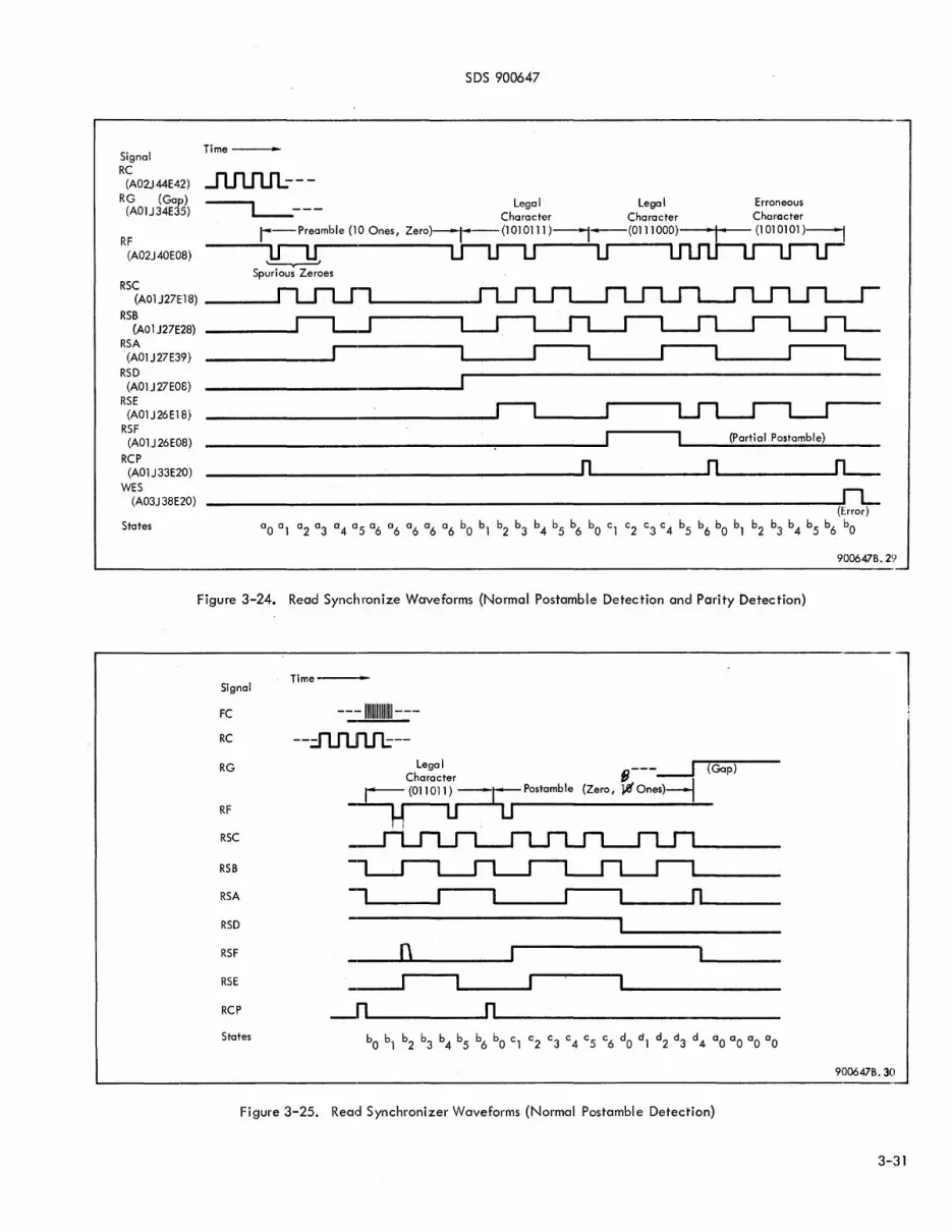
Signal RC
(A02J44E42)
RG (Gap) (AOlJ34E35)
RF (A02J40E08)
RSC
SDS 900647
Time---
Legal Legal Character Character
~-Preamble (10 Ones, Zero}-<-.....--(1010111)--j-(0111000)
----u-u--Spuriou; Zeroes
(AOlJ27E18) ___ __
RSB (AO 1 J27E28)
RSA (AOlJ27E39)
RSD (AOlJ27E08)
RSE (AOlJ26E18)
RSF (AOl J 26E08)
RCP (AOlJ33E20)
WES (A03J38E20)
States
--------',
(Partial Postamble)
________________________________ ~n~ ________ ~n~ _________ ~
Figure 3-24. Read Synchronize Waveforms {Normal Postamble Detection and Parity Detection}
Signal
FC
RC
RG
RF
RSC
RSB
RSA
RSD
RSF
RSE
RCP
States
Time---
---11111111111111---
--=IlIlIlIl.:--Legal e--- I (Gap)
Character ----J -Hr---- (011011) -. r Postamble (Zero, }If Ones}--j
U lLr---------------~, i
-,---- _______ n~ ______ _
o _------1 ~~ ________ n~ ______________________ __
Figure 3-25. Read Synchronizer Waveforms {Normal Postamble Detection}
900647B.29
-l
900647B.30
3-31

Paragraph 3-204
Signal
RC
RG
RF
RSC
RSB
RSA
RSD
RSF
RSE
RCP
WES
States
SDS 900647
Time---a-
--~--
___________ (;...N_o_G_a..:,.p.;...) ---------lH~--1 (Gap)
t--Illegal Character -t-- Next Character--l _.......;1_ (0111111) 1 (101 0111r--i-) _____ I_--li ,-"pJ------
U u-u U ,(
~----~~J__------
~ ---, .... _------ ~~
~----------------~H~----~~
~----------------lH~-------
~~----------------------------lH~-----_________________ --', (Error) ~~
900647B.31
Figure 3-26. Read Synchronizer - I)etector Waveforms (Premature Postamble Detection)
Time---Signal
FC --::fUUUl=--RG
RSD
RSE
WES _________________ ~r---l~ __
(Error)
900647B.32
Figure 3-27. Read Synchronizer - Detector Detailed Waveforms (Premature Gap)
3-32
When a gap occurs in any state, the counter returns to a II zeroes:
kRSA RG + - - -
kRSB RG + - - -
kRSC RG + - - -
In state a1' the counter will stall until a legal preamble one is decoded:
jRSB = RSC (RSD + RSF + RF) RG
kRSC = RSC (RF + - - -) + - - -
The arrival of a one lets the counter proceed to a2 and then a3 regardless of the content of RF:
jRSC = (RSA + RSB) RG
3-204 This process continues, while the read decoder confirms every other bit as a preamble one until state a6 is reached. A certain tolerance to the incoming bits is thus
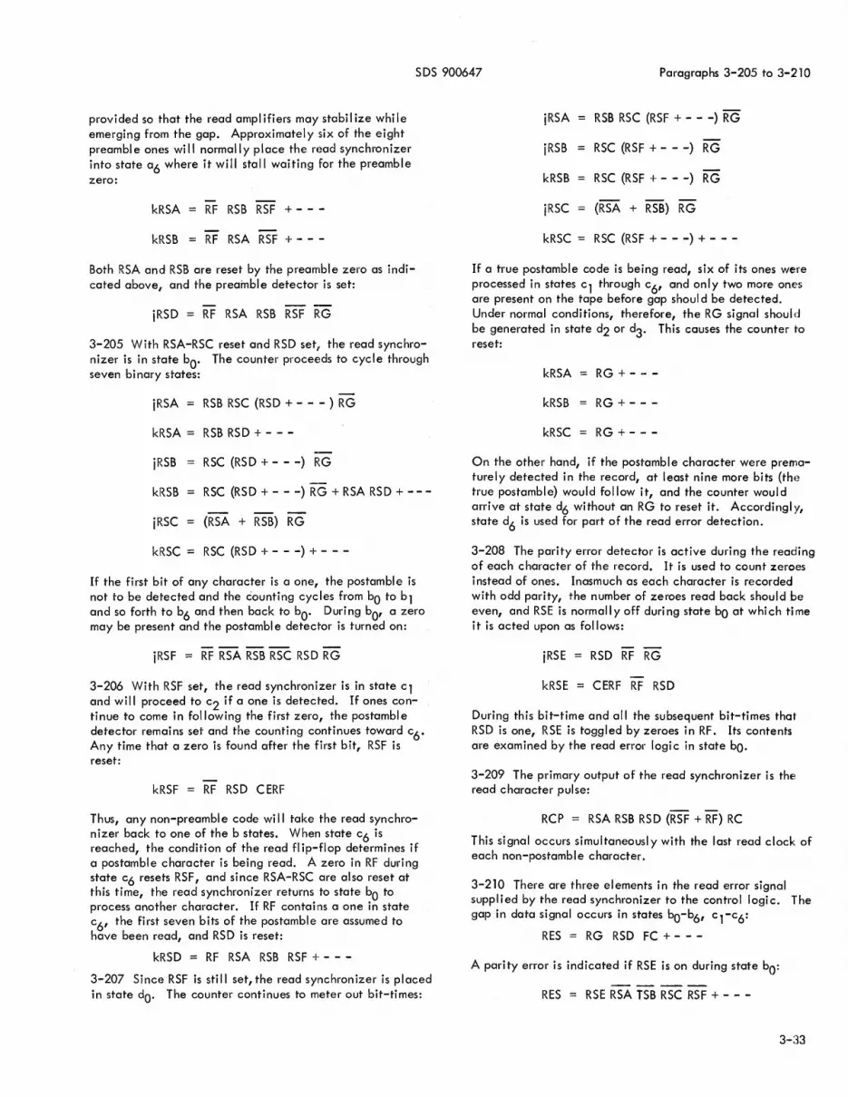
SDS 900647 Paragraphs 3-205 to 3-210
provi ded so that the read ampl ifiers may stabil ize whi I e emerging from the gap. Approximatel y six of the eight preamble ones will normally place the read synchronizer into state a6 where it will stall waiting for the preamble zero:
kRSA RF RSB RSF + - - -
kRSB RF RSA RSF + - - -
Both RSA and RSB are reset by the preamble zero as indicated above, and the preainble detector is set:
jRSD = RF RSA RSB RSF RG
3-205 With RSA-RSC reset and RSD set, the read synchronizer is in state boo The counter proceeds to cycle through seven binary states:
jRSA = RSB RSC (RSD + - - - ) RG
kRSA = RSB RSD + - - -
jRSB
kRSB
jRSC
RSC (RSD + - - -) RG
RSC (RSD + - - -) RG + RSA RSD + - --
(RSA + RSB) RG
kRSC RSC (RSD + - - -) + - - -
If the first bit of any character is a one, the postamble is not to be detected and the counting cycles from bO to b1 and so forth to b6 and then back to boo During bO' a zero may be present and the postamble detec:tor is turned on:
----jRSF = RF RSA RSB RSC RSD RG
3-206 With RSF set, the read synchronizer is in state c1 and will proceed to c2 if a one is detee-ted. If ones continue to come in following the first zero, the postambl e detector remains set and the counting continues toward c6' Any time that a zero is found after the first bit, RSF is reset:
kRSF = RF RSD CERF
Thus, any non-preambl e code wi II take the read synchronizer back to one of the b states. When state c6 is reached, the condition of the read fI ip-flop determines if a postamble character is being read. A zero in RF during state c6 resets RSF, and since RSA-RSC are also reset at this time, the read synchronizer returns to state bO to process another character. If RF conta ins a one instate c6' the first seven bits of the postamble are assumed to have been read, and RSD is reset:
kRSD = RF RSA RSB RSF + - - -
3-207 Since RSF is still set,the read synchronizer is placed in state dO' The counter continues to meter out bit-times:
jRSA RSB RSC (RSF + - - -) RG
jRSB R SC (R S F + - - -) RG
kRSB R SC (R S F + - - -) RG
jRSC (RSA + RSB) RG
kRSC RSC (RSF + - - -) + - - -
If a true postamble code is being read, six of its ones were processed in states c1 through c6' and only two more ones are present on the tape before gap shoul d be detected. Under normal conditions, therefore, the RG signal should be generated in state d2 or d3 . This causes the counter to reset:
kRSA RG + - - -
kRSB RG + - - -
kRSC RG + - - -
On the other hand, if the postamble character were prematurely detected in the record, at least nine more bits (the true postamble) would follow it, and the counter would arrive at state d6 without an RG to reset it. Accordingly, state d6 is used for part of the read error detection.
3-208 The parity error detector is active during the reading of each character of the record. It is used to count zeroes instead of ones. Inasmuch as each character is recorded with odd parity, the number of zeroes read back should be even, and RSE is normally off during state bO at which time it is acted upon as follows:
jRSE = RSD RF RG
kRSE = CERF RF RSD
During this bit-time and all the subsequent bit-times that RSD is one, RSE is toggled by zeroes in RF. Its contents are examined by the read error logi c in state bOo
3-209 The primary output of the read synchronizer is the read character pulse:
RCP = RSA RSB RSD (RSF + RF) RC
This signal occurs simultaneously with the last read clock of each non-postamble character.
3-210 There are three elements in the read error signal suppH ed by the read synchronizer to the control logic. The gap in data signal occurs in states bO-b6, cl-c6:
RES = RG RSD FC + - - -
A parity error is indicated if RSE is on during state bO:
RES = RSE RSA TSB RSC RSF + - - -

Paragraphs 3-211 to 3-217 SDS 900647
The occurrence of a premature postamble is detected if state d6 i sreached:
RES = RSA RSB RSD RSF + - - -
3-211 HARVEY REGISTER LOGIC DESCRIPTION
3-212 A seven-stage Harvey register is included in the tape control unit to perform the functions of parallel-toserial conversion and serial-to-parallel conversion, and also to provide timing signals for starting, stopping, and continuing sequences.
3-213 The basic timing-sharing is achieved by four gates: SFG, SRG, SPG, and CBG. Either the shift forward gate or shift reverse gate may be true during CS2 or CS7, the writing and reading control states respectively:
SFG CS27 C 12M CECF
SRG CS27 C 12M CECF
The C 12M fl ip-flop remembers the direction of tape motion. The external clock flip-flop CECF is used for parallel transfers to the Harvey register and must be reset for serial shifting. The shift parallel gate is true only during writing and then 6nly when a character is being clocked by CECF from the buffer:
SPG = CS2 CECF
In control states 0, 4, 5, 6, the Harvey register is converted to a binary counter under the control of the count binary gate:
CBG = CSO + (CS4 + CS56) C ECF
In control states 4, 5, 6, the external clock flip-flop is used to c iear the Harvey register pri or to counti ngi therefore, CECF must be reset to enable CBG.
3-214 Time-shared clocking of the Harvey register is accomplished by two generalized pulse gates, SSP and SPP. The shift serial pulse is derived from the write clock generator during writing:
SSP = CS2 WCPO + - - -
During reading, the read decoder suppl ies the read clock for shifting:
SSP = CS7 RC + - - -
The shift parallel pulse is controlled primarily by CECF, and the logic can be expanded as follows:
spp
3-34
- --CSO CS7 CECF FC
(CS1 + CS2 + CS3 + CS4 + CS5
+ CS6) CECF FC
Using this expanded form, it should be noted first that the Harvey register is not active in CS 1 or CS3. In CS2, the SPP is used to clock characters from the computer buffer into the HR. In the beginning of control states 4, 5, 6, and C ECF is on, and the SPP is used to reset the Harvey register to all zeroes prior to binary counting.
3-215 The seven stages in the Harvey register are all connected as repeaters. A character is transferred in parallel from the computer buffer as follows:
dHROO SPG RP + - - -
dHR01 SPG R1 + - --
dHR02 SPG R2 + - - -
dHR03 SPG R3 + - - -
dHR04 SPG R4 + - - -
dHR05 SPG R5 + - - -
dHR06 SPG R6 + - - -
cHROO SPP + - - -I I I
cHR06 = SPP + - - -
3-216 Shifting forward is performed under the control of the following logic:
dHROO SFG HROl + - - -
dHR01 SFG HR02 + - - -
dHR02 SFG HR03 + - - -
dHR03 SFG HR04 + - - -
dHR04 SFG HR05 + - - -
dHR05 SFG HR06 + - - -
dHR06 SFG HRIN
cHROO SPP + - - -I I I
cHR06 = SPP + - - -
3-217 In order to duplicate file mark codes, it is necessary to preserve the contents of the Harvey register by rec irculation:
HRIN = W9 HROO + - - -
During read/scan forward operations the HR06 receives the output of the read flip-flop serially:
H RIN = W9 RF + - - -

SDS 900647 Paragraphs 3-218 to 3-226
3-218 Shifting for scan reverse operations is performed under the control of the following logi c:
dHROO SRG RF + - - -
dHR01 SRG HROO + - - -
dHR02 SRG HR01 + - - -
dHR03 SRG HR02 + - - -
dHR04 SRG HR03 + - - -
dHR05 SRG HR04 + - - -
dHR06 SRG HR05 + - - -
cHROO SSP + - - -I I I
cHR06 = SSP + - - -
3-219 For counting in binary, the repeClter inputs are con-nected to self-terms for steering:
dHROO CBG HROO + - - -
dHR01 CBG HR01 + - - -
dHR02 CBG HR02 + - - -
dHR03 CBG HR03 + - - -
dHR04 CBG HR04 + - - -
dHR05 CBG HR05 + - - -
dHR06 CBG HR06 + - - -
The clock inputs are connected for forward transition binary counting clocked at the least signifi cant stage by WGO 1 (1. 6 kc):
cHROO CBG WG01
cHR01 CBG HROO
cHR02 CBG HR01
cHR03 CBG HR02
cHR04 CBG HR03
cHR05 CBG HR04
cHR06 CBG HR05
3-220 For resetting the Harvey register prior to counting at the beginning of CS4, CS5, or CS6, the external clock fl ip-flop is set making SFG, SRG, and CBG zero. Since
SPG is qual ified by CS2, it is also zero so that all repeater inputs are false. The SPP is made true, however, so the Harvey register gets a clock pulse to reset it to all zeroes.
3-221 Since Harvey register logic requires inverter inputs to all stages, each term is mec;hanized in complementary form. This necessitates a control term which, though it does not appear in the equations, prevents erroneous input terms from appearing. This is called the Harvey register gate:
HRG = SFG SRG SPG CBG
The HRG participates in the mechanization as indi cated in the following example:
dHROO = SFG HR01 + SRG RF + SPG RP
+ CBG HROO
SFG HR01 + SRG RF + SPG RP
+ CBG HROO + HRG
3-222 CONTROL LOGIC DESCRIPTION
3-223 Introduction
3-224 The functions performed by the tape control unit in each control state are summarized in figure 3-35 and table 3-4 (located near the end of this section). Test Point 1 (A01 J45 E02) is the output of a digital-to-analog converter which can be used to monitor the control states.
3-225 Selection and Starting (CSO)
3-226 A MAGPAK tape process is selected and started by executing an appropriate EOM command. A summary of these commands is given in section II of this manual. The following description begins with MAGPAK not selected by the buffer. It is held in CSO:
rCSA rCSB = rCsc (W 11 STRT) dc
CSO CSA CSB CSC
The IDLE-READY state is maintained because C ECF is held reset:
rC ECF = (W 11 STRT) dc
A general ized start command is generated for tape commands addressed through the buffer:
STRT = BUC C 17 C20
The appropriate tape motion control signal is submitted to the tape transport unit electronics. Forward motion is activated by Tl2S:
T12S = STRT C 12 Q2
3-35
Paragraphs 3-227 to 3-231 SDS 900647
and reverse motion is activated by S 12T:
S12T = STRT C12 Q2
The tape reverse monitor fl ip-flop is set to remember reverse operations. It is held reset prior to buffer selection:
sC12M STRT C 12
rC 12M Wll
3-227 The least significant octal digit in the computer Cregister is decoded into logical tape unit addresses and forwarded to the tape transport unit:
L.LTO = C21 C22 C23 I I I
LLT7 = C21 C22 C23
The tape transport unit selects the appropriate transport according to the UNIT SELECT switch position. The TSA or TSB dc flip-flop for the selected transport is set for forward or reverse motion, respectivel y. As selection is establ ished, the tape transport un it returns a sel ect signal over the SELS bus. The 9448 departs IDLE-READY when the command loop is closed.
jCECF = CSO STRT SELS + - - -
cCECF = FC
With CECF set as a result of , selection, the write clock generator starts counting:
jWCD kWCD CSG
cWCD
CSG CECF + - - -
The buffer is addressed for tape unit operation, so the write synchronizer is allowed to count:
rWSA = rWSB = rWSC = 0N 11) dc
These two counters produce WGO 1 pulses at 1.5 kc:
WCPO = WCA WCB WCD CSG FC
WGO 1 = WSA WSB WCPO
The Harvey register counts forward in binary in control state 0 clocked by WG01 (1. 5 kc):
CBG = CSO + - - -
cHROO= CBG WG01 + - - -
3-228 Certain safety features are mechanized in the tape control unit and should be introduced here. If for any
3-36
reason a start command is not honored by the 9446 Tape Transport Unit, the buffer is halted. Thus, if a reverse command is given at the beginning of tape or if the unit is not ready, the 9446 refuses to select and SELS is not made true. This condition is detectable if SELS is not true after Q2 in the computer has elapsed during a start command:
@ = SELS AANS Q2 STRT + - - -
The address acknowledge signal AANS is present to precl ude halting if no transport UNIT SELECT switches are set to the value corresponding to the start command address (C21-C23). AANS is incl uded above because of the requirements of the auxi I iary control logic.
3-229 Logic is also provi ded to halt the buffer if the 9446 transport deselects in CS1, CS2, CS3, CS4, or CS7:
CSO CS56 SELS TEST + - - -
CS56 CS5 + CS6
Accordingly, in a scan reverse or erase reverse, if the beginning of tape clear space is encountered, SELS will go false and the buffer is halted. Any other condition that disqualifies SELS in the 9446 will likewise produce a halt signal.
3-230 Write or Erase Forward (CSO)
3-231 The write tape control signal is generated and sent to the transport electroni cs to enable the selected write ampl ifier to appl y write current:
WRTS = W9 SELS
The erase tape fl ip-flop is turned on:
sCETF = CSO W9 Wll WCP1 + - - -
Control state 0 is maintained for 36.0 milliseconds for write or erase forward (see figures 3-28 and 3-29). This allows time for the forward pressure roller to engage the tape, accelerate it to 7.5 ips, and move the nominal 0.225 inch required to complete the erasure of the gap. To accom-pi ish the necessary delay, the start gap delay is decoded from the Harvey register:
STGD = HR05 HR04 HR02 HROO WG01
Following the 36.0-millisecond delay, the 9448 enters control state 1 to write the preamble:
jCSC = CSO W9 STGD + - - -
cCSC = WG01
CS1 CSA CSB CSC
SDS 900647 Paragraphs 3-232 to 3-234
,-------------------...----------------------"---"-
Signal Time----
r::=::::11--30 msec CS6-CS5-CS4-CS3-CS2-CS1-
I _~~:.£::;===::j 1 r-----i- I r-----J
TPl CSO (A03J45E02)
36msec -I.~I-.--
I r' I,---n .. --I ....
STRT (A03J 29E 39) ______ n~~~~------------~~~~--------------------------Start Forward
9006476.33
Figure 3-28. Write Forward Control State Sequence
r--------.--------------------------------------------------------------------------------.
Signal Time ----...... -
1. 3msec1 ,,"-_~""---"""f-r- 30msec CS6-CS5-CS4-CS3-CS2-CS1-
26msec I l o 3m,eel i
--36-m-sec-::.I:.-::.: ...... ~D_oo 7n msee I I r-tl-u
TP1 CSO (A03J45E02)
STRT (A03J 29 E 29) ___ ~n~ __ ~ ____ ~ ________ ~r~I __ ~r~,~-------------
Start Forward \. J
Continue
9006476.34
Figure 3-29. Erase Forward Control State Sequence
3-232 Write or Erase Forward (CS 1)
3-233 Reading is enabled:
sCERF = CS13 + - - .•
Control state 1 lasts for 14 bit-intervals under the control of CECF which is left set from CSO. The erase tape flipflop is reset after the fifth bit-interval in a write operation:
rCETF = CS1 WlO WSA WSC WCP1
The write fl ip-flop is gated onto the write data bus:
WDAS = CETF WF
It is toggles by write clock phase 1 to loy down synchronizing transitions for the preamble ones:
jWF
cWF
kWF = W9 CSG
WCP1 + - - -
At the seventh bit-interval, WGO 1 resets CECF for the second character time 0 f CS 1:
kCECF CS 13 WGO 1 + - - -
CS13 CSA CSC
Six more ones are written by WF, and the preamble zero transition is inserted in the last recorded bit:
cWF = WCP1 + CS1 CECF WSA WSB WCOO + - - -
3-234 At the same time, the 9448 goes to control state 2 for writing the record or for timing the erasing of the record:
JCSB
kCSC
cCSB
CS2
CS 1 C ECF + - - -
CS1CECF+--
cCSC = WG01
CSA CSB CSC

Paragraphs 3-235 to 3-238 SOS 900647
As the 9448 enters CS2, the external clock fl ip-flop is set to request the first character from the buffer:
jCECF CS13 WG01 + - - -
cCECF
While in CS1, the continue flip-flop, skip-remainder flipflop, and file mark flip-flop are all initialized to zero:
rCUFF CS 13 + - - -
rCSRF CSBWCP1+---
rCFMF CS 13 + - - -
CS13 CSA CSC
3-235 Write or Erase Forward (CS2)
3-236 In control state 2, the actual record is written {or erased}. The external clock flip-flop, which was set for the first character in CS1, provides the clock to the computer buffer:
@ = CS27 CERF CSRF CECF + - - -
CS27 CS2 + - - -
Each character is transferred to the Harvey register in parallel:
dHROO
dHR01 I I I I I
dHR06
cHROO
I I I I I
cHR06
SPG RP + - - -
SPG R 1 + - - -I I I I I
SPG R6 + - - -
SPP + - - -
SPP + - - -
SPG CS2 CECF
SPP CSO CS7 CECF FC
The buffer responds to the c lock by making W6 true, which resets C EC F :
kC EC F = C S27 W 6 + - - -
cCECF = FC
CS27 CS2 + - - -
3-38
With CECF reset, the Harvey register starts shifting clocked by WCPO:
dHROO SFG HR01 +- --
dHR01 SFG HR02 + - - -I I I I I
dHR05 SFG HR06 + - - -
cHROO SSP + - - -, I I
cHR06 SSP + - - -
SFG CS27 C12M CECF
SSP C S2 W CPO + - - -
CS27 CS2 + - - -
The serial ized character appearing in HROO is encoded by WF:
kWF W9 CSG
cWF WCP 1 + CS2 HROO WCPO + - - -
In write operations, WF is applied on the write data bus to the tape transport unit electroni cs. An erase operation sustains a dc logical zero:
WOAS CETF WF
3-237 In a normal write or erase process, the foregoing sequence is repeated for each output character. When the file mark code is written, however, only one character is supplied by the buffer. A combination of idiosyncrasies in conventional recording on SOS magnetic tape unit {such as Models 9246 and 9146}, causes the reading of the file mark to appear as two identical characters. (In particular, the buffer is arranged so that it will not honor a gap signal until two or more characters are read. The longitudinal, evenparity check character in conventional formats is therefore read as the second character in a fi Ie mark.) Inasmuch as MAGPAK must be compatibl e with programs written for these other transports, the fi Ie mark character must be recorded in duplicate for subsequent reading operations.
3-238 The normal write sequence {more than one character} is characterized by the fact that W5 in the buffer is false following all character transmissions except the last {see figure 3-30}.
This fact is remembered by the continue flip-flop:
sCUFF CS2 W5 WSB WCP 1 + - - -

SDS 900647 Paragraphs 3-239 to 3-242
Signal Time •
~ __ ~n _____________________ ~nL-WG01 (A023J44E07) Jl H
L CS2
.....J H (A02J 37E35)
~ ____ ~r--l ____________________ ~r-CECF 51 (A02J26 E08) H
W5 n (A03J32E36) H WO
(A03J31 E33) n CUFF n
(A02J27E29) r CSRF
(A02J 27E43) CFMF
H (A02J27E15) ~~
9006478.35
Figure 3-30. Normal Write Sequence
The external clock flip-flop is set after the serial recording of each character by WGO 1:
iCECF CS2 (CUFF +.- - -) WG01+---
cCECF FC
This calls for the transmission of the next character from the buffer, and the sequence is repeated as required.
3-239 In the file mark write sequence, on the other hand, W5 will be true after the first character is transmitted and CUFF is left reset (see figure 3-31). CSRF is set at the end of the fi rst character ti me by the I eadi ng edge of WGO 1 :
sCSRF C52 CUFF WGOl + - - -
With C5RF set, the external clock fl ip-f1op cannot get through to the buffer:
C527 CERF CSRF CECF + - - -
The file mark code was recirculated in the Harvey register during the previous character time:
dHR06 5FG HRIN + .- - -
HRIN W9 HROO + - - -
This code is shifted through the Harvey register again and encoded onto the tape a second time.
3-240 Escape from control state 2 is controlled by the buffer. When the last character is transmitted, W5 is left true as part of the halt interlock condition. In the normal write sequence, CUFF is set and the 9448 goes to C53.
jC5C
C53
C 52 W 5 C UF F + - - -
C5A C5B C5C
When a file mark is written, C5RF gets set at the end of the first character time and the file mark flip-flop is turned on four bit-times later while the file mark character is repeating:
sCFMF C52 W5 C5RF W5A WCPl + - - -
With CFMF set, the 9448 will enter C53 even though CUFF was left reset:
jC5C C52 W5 CFMF + - - -
In either write sequence, normal or file mark, CECF is turned on to control the duration of CS3:
jCECF
cCECF
C52 (CUFF + CFMF) WGO 1 +- -
FC
3-241 Write or Erase Forward (C53)
3-242 In control state 3, the postamble code is written in a manner similar to that used for the preamble in C51.
3-39

Paragraph 3-243 SDS 900647
Signal Ti me -----1 .. _
WGOl (A02J44E07)
Jl _____________________ n~ __________________ ~nL CS2
(A02J37E35) ~ L CECF
(A02J 26E08) JI r W5
(A03J 32E36) WO
(A03J3l E33) CUFF
(A02J 27E29) CSRF
(A02J27E43) CFMF
(A02J27El5)
900647B.36
Figure 3-31. Fi Ie Mark Write Sequence
Since CECF is on for the first character time, the postamble zero transition is encoded in WF as the first bit:
jWF kWF = W9 CSG
cWF WCPl + CS3 CECF WSA
WSB WSC WCPO + - - -
Afterwards, WF is clocked only by WCPl producing the postamble ones. The external clock fl ip-flop gets turned off at the ~nd of the first seven bit-times:
kCECF CS13WG01+---
cCECF
CS13 CSA CSC
Two more bit-times of ones are recorded, and then the erase tape 'flip-flop is set to terminate the postamble code emitted on WFAS:
sCETF CS3 CECF WSB WCP1 + - - -
WDAS CETF WF
If an erase operation is in progress, C ETF was never turned off in CS 1 and dcerasing is accompl ished throughout CS I, CS2, and CS3.
3-40
3-243 With CECF reset, the 9448 is free to depart CS3 at the end of the character time. For a writing sequence, control state 4 is entered.
jCSA
kCSB
kCSC
C S 3 C EC F + - - -
CS3CECF+---
C S3 W 1 0 C EC F + - - -
cCSA cCSB = cCSC = WGOl
Since the reset input to CSC is qualified for the non-erase condition, it will remain set as the 9448 departs CS3 in an erase sequence. The effect is to take the control state counter to CS5 instead of CS4:
CS4 CSA CSB CSC
CS5' CSA CSB CSC
In either sequence, CECF is set as the 9448 leaves CS3 in order to provide cI earing of the Harvey register in CS4 or CS5:
jCECF
cCECF
CS13 WGOI + - -
FC
CS13 CSA CSC
Incidentally, the continue flip-flop is reset in CS3 to permit a continue sequence in CS5:
rCUFF
CS13
CS 13 + - - -
CSA CSC

SDS 900647 Paragraphs 3-244 to 3-249
3-244 Write or Erase Forward (CS4)
3-245 The read enable flip-flop is set in control state 1:
sCERF CS13
C:S 13 CSA CSC
The read-after-write test is therefore started I ust before the writing of the preamble:
gRSF 1 = gRSF2 = CERF
clRSF1 RDAS TEST + •. - -
eRDA cRDB = cRDC =: cRDD = Fe
eRSA cRSB = cR5C = RC + RG FC
rRSE rRSF = (STRT + C ERF FC) dc
The distance between the write and read hecid is 0.3 inch, which corresponds to 60 characters or about 15 words at 4 characters perword. Accordingly, the read synchronizer will detect the preamble code while the 9448 is In C52 if the record is longer than 15 words. When writing of the record is completed, the read synchronizer should not confirm the postamble until approximately 40 milliseconds have elapsed corresponding to the time required for the tape to traverse the interhead distance at 7.5 ips.
3-246 Control state 4 is inserted in the write sequence primarily to allow time for the record to traverse the interhead distance. When the read synchronizer detects gap, presumably in CS4 after confirming the postamble, CERF is reset:
rCERF = CSA CUFF (RSF + - - -) RGFC + - - -
If a gap occurs after the preamble is detected, CERF is reset anyway:
rCERF = CSA CUFF (RSD + - - -) RGFC + - - -
3-247 A premature gap does produce an error signal to the buffer:
RES RG RSD FC + - - -
RES + - - -
but a premature stopping sequence as a resul t of the earl y gap woul d be very dangerous to previous records if it were followed by an erase reverse operation. Accordingly, CS4 is timed out to 34.7 mill iseconds, or about 10% less than ' the expected interhead tape motion time, before the gap is honored. This is the write-to-read delay, WTRD, produced in the Harvey register:
WTRD HR05 HR04 HROl HROO WG01
WTRD can be true at many counts after the 34. 7-mill isecond point is reached. The Harvey register is reset to zero by CECF which was set in CS3 or CS7:
cHROO I I I
cHR06
SPP
Spp + - - -
Spp + - - -
--CSO CS7 CECF FC
(All repeater input gates are false at this time, so the register is clocked to zero. )
3-248 After one-half of a bit-time interval, C ECF is reset:
kCECF
cCECF
(CS4 + - - -) WCPl
FC
The Harvey register converts to a binary counter c locked by WG01:
CBG (CS4 + - - -) CECF + - - -
When the WTRD count is reached, the control state counter can proceed to CS5 as soon as CERF is reset by the gap:
·CSC I ' CS4 W9 W10 CERF WTRD + - - -
cCSC WGOl
CS5 CSA CSB CSC
Control state 5 will be entered as WTRD occurs if the gap occurred earl y.
3-249 Another condition could exist; namely, the gap is not detected. This will happen if erasure is not completed or no information is recorded because of dirt under the write head. The 9448 stays in CS4 waiting for CERF to reset, but onl y for a total of 50.7 mill iseconds. This time interval, called the interhead guard delay, is recognized in the Harvey register:
IHGD HR06 HR03 HROl HROO WGO 1
Thus, about 25% additional time is allowed beyond the nominal interhead motion time after which the control state counter escapes to CS5:
jCSC
cCSC
CS5
C S4 W 10 I H G D + - - -
WG01
CSA CSB CSC
An overdue gap error signal is sent to the buffer
@ RES + SELS WES9
Res CS4 WlO IHGD + - - -
3-41

Paragraphs 3-250 to 3-255 SDS 900647
In any case, C ECF is set in order to provi de clearing of the Harvey register in CS5:
jCECF = C54 CERF WTRD W9 WlO C 12M SELS
+ C S4 I H G D + - - -
cCECF = FC
3-250 Write or Erase Forward (CS5)
3-251 Control state 5 provides the necessary delay to erase the last part of the 0.75-inch gap. In CSO, 0.225 inch of gap is generated. The interhead distance of 0.3 inch is erased in CS4. That leaves 0.225 inch of tape to be erased in the stopping sequence. The stop distance is approximately 0.03 inch, so CS5 lets the tape run at 7.5 ips for O. 195 inch before the stop command is given. The required time interval is 26.0 milliseconds, and is called the stop gap delay:
SPGD HR05 HR02 HR01 WG01
The Harvey register is reset to zero by CECF which was set in CS4 or CS7:
cHROO I I I
cHR06
SPP
SPP + - - -
SPP + - - -
CSO CS7 CECF FC
(All repeater input gates are false at this time, so the register is clocked to zero. )
3-252 After one-half of a bit time interval, CECF is reset:
kCECF (CS5 + - - -) WCP 1 + - - -
cCECF FC
The Harvey register converts to a binary counter clocked by WGOl (1. 5 kc):
CBG (CS56 + - - -) CECF
CS56 CS5 + - - -
When the SPGD count is reached, the control state counter can proceed to CS6 if a continue command is not received:
JCSB CS5 SPGD CUFF + - - -
kCSC CS5 SPGD CUFF + - - -
cCSB cCSC = WG01
CS6 CSA CSB CSC
3-42
3-253 In CS5 (before SPGD), if the computer program tests for gap (SKS12610), an affirmative reply will be given:
@= C12 C13 C14 C15 C16 CS5 CUFF CFMF + - - -
A new start command may be given which calls for continuation of tape motion without stopping. A start command in CS5 will set the continue fl ip-flop:
sCUFF CS5 STRT + - - -
The stop gap delay is ignored by the logic if CUFF is on. Instead the Harvey register continues to count, providing a time interval corresponding to 0.75 inch of tape travel at 7.5 ips less the interhead distance already traveled in CS4. The required delay is 60.7 mill iseconds and is called the continue write delay:
CUWD HR06 HR04 HR03 HRO 1 WGO 1
At the CUWD count, the control state counter goes back to control state 1 to write the preamble for the next record:
kCSA CS5 W9 CUFF CUWD
cCSA WG01
CS1 CSA CSB CSC
The external clock fl ip-flop must be set to prepare for its roll in controlling the duration of CS1:
jCECF CS5 W9 CUFF CUWD + - - -
3-254 Write or Erase Forward (CS6)
3-255 In the absence of the continue command, the control state counter goes from CS5 to CS6 when the stop gap delay has been timed out. In control state 6, the STOP command line is made true to the tape transport unit electroni cs:
STOP HR05 CS6 + - - -
The Harvey register is reset to zero by CECF, which was set in CS5 for write or erase forward sequences:
cHROO I I I
cHR06
Spp
SPP + - - -
Spp + - - -
--CSO CS7 C ECF FC
(All repeater input gates are false at this time, so the register is clocked to zero.)
After one-half of a bit time interval, CECF is reset:
kCECF
cCECF
(CS6 + - - -) WCP1 + - - -
FC
SDS 900647 Paragraphs 3-256 to 3-258
The Harvey register converts to a counter clocked by WGO 1 (1. 5 kc):
CBG (CS56 + -- -) CECF + - - -
CS56 CS6 + - - -
3-256 With the STOP line true, the forward pressure roller disengages and the tape comes to a stop. When the Harvey register has counted to 32, HR05 is turned on, removing the STOP signal. The duration of the STOp'signal is thus establ ished af' 21. 3 mill iseconds, whi ch allows ample time to stop the tape. At the fall of the STOP signal, the transport deselects, making the SELS bus go false. The write tape signal is dropped, removing write current:
WRTS W9 SELS
The Harvey register continues to count unti I the stop tape delay is recognized 9.0 milliseconds later:
SPTD HR05 HR03 HR02 HROO WGO 1
At this time the skip remainder fl ip-flop gets set:
sCSRF CS6 SPTD + - - -
The halt signal is sent to the buffer:
Whs CS6 CSRF + - - -
W hen the buffer resets its address lines in response to the halt signal, the control state counter returns to CSO:
-_._-rCSA rCSB = (W 11 STRT) dc
eso CSA CSB CSC
Signal Time---a-
3-257 Read or Scan Forward (CSO)
3-258 In the stopped condition, the beginning of the next record is 0.525 inch from the read head. In order to avoid spurious information that might be in the gap, the read logic is not enabled until 50.7 milliseconds after the STRT com-' mand is executed (see figure 3-32). The delay is accomplished by holding the 9448 in control state 0 until the Harvey register has counted to the code recognized as the interhead guard delay:
IHGD HR06 HR03 HROl HROO WGOl
After the 50.7 mill iseconds have elapsed, the control state counter goes directly into CS7 from CSO:
jCSA C SO I H G D + - - -
jCSB C SO I H G D + - - -
jCSC CSOIHGD+---
cCSA cCSB = cCSC = WGOl
CS7 CSA CSB CSC
Since CUFF is held set before the buffer selects tape unit operations, its output will be true as the 9448 departs CSO:
sCUFF Wll+---
The external clock flip-flop is reset at the end of CSO in read or scan forward operations:
kCECF
cCECF
CSOIHGD+--
FC
CS7-
CS6-
CS5-
CS4-
CS3-
CS2-
CS1-
'" ----~\ r-------, I I
(20+0. 7n) __ I I I msec ----- ---I L. ____ _
26m,ec-L-J -30m,ec
L75.5 m,ec-+---J
1--50.7msec-/ ~ __ ~ ____________ ~~r~,~ __ ~r~,~ _____________________________________________ __
Start Forward '--v---'
TPl CSO (A03J 45E02)
STRT (A03J29E39)
Continue
900647B.37
Figure 3-32. Read/Scan Forward Control State Sequence
3-43

Paragraphs 3-259 to 3-263 5D5900647
3-259 Read or 5can Forward (C57)
3-260 The actual reading of a record is performed in control state 7. The read enable flip-flop is set by CUFF, which was left true in CSO and made true in C55 for conti nued operations:
sCERF C57 CUFF + - - -
The file mark flip-flop is also armed at the beginning of C57:
sCFMF C57 CUFF + - - -
After performing the job of setting C ERF and CFMF at the beginning ofC57, CUFF is reset:
rCUFF C57 WCP1 + - - -
With CERF set, the read decoder can supply bits through RF into the read synchronizer, which in turn detects the preamble:
jRSD RF R5A R5B R5F RG
cR5D RC + - - -
3-261 The read fl ip-flop is also connected to the Harvey register:
HRIN W9 RF + - - -
which shifts forward clocked by RC:
dHROO SFG HR01 + - - -I I I I I I
dHR05 5FG HR06 + - - -
dHR06 SFG HRIN + - - -
cHROO SSP + - - -I I I
cHR06 SSP + - - -
----SFG CS27 C 12M CECF
C527 CS7 + - - -
S5P CS7 RC + - - -
With RSD set, the read synchronizer counts through 7-bit cycles and produces the read character pulse:
RCP RSA RSB RSD (R5F + RF) RC
The external clock fl ip-flop is set as the seventh bit of each character is shifted into the Harvey register:
3-44
jCECF
cCECF
CS7 RCP + - - -
~
This c locks the buffer:
C527 CERF C5RF CECF + - - -
CS27 CS7 + - - -
The contents of the Harvey register are transferred in parallel to the buffer:
© I I I
@ @
CS7 HROl I I I
CS7 HR06
CS7 HROO
When W6 is made true in the buffer, the external clock flip-flop is reset:
kCECF C527 W6 + - - -
cCECF
CS27 C57 + - - -
3-262 If a non-fi Ie mark code is present in the Harvey register at the time a character is transferred to the buffer, the file mark fl ip-flop is reset:
rCFMF CS7 W5 W6 FMCD + - - -
----FMCD HROO HR01 HR02 HR03 HR04
HR05 HR06
A gap in the record also wi II prevent a file mark from being detected:
rCFMF R S D R G FC + - - -
If a true fi Ie mark is present, CFMF will remain set through the end of the record. The fi Ie mark fl ip-flop may be tested by the program using the SKS 13610 instruction:
C12 C13 C14 C15 C16 CUG
CFMF + - - -
3-263 Characters continue to be transferred to the buffer until the end of the record unless the program executes an EOM 1361 0 to skip the remainder of the record. The skip remainder fl ip-flop is set by this instruction:
sC5RF
CNTL
CS7 CNTL (C12 C13 C14 C15
C 16) + - - -
Ioc C 17 C20
The buffer may receive no more clocks:
@C-S-2-7-C-E-R-F-=C=S=RF=--C-EC-F-+------

5D5 900647 Paragraphs 3-264 to 3-271
Whenever the gap is detected, the read enable fl ip-flop is turned off:
rCERF C5A CUFF (R5D + R5F) RG FC + ... - -
This also inhibits clocks to the buffer ane! permits the control state counter to escape from C57. In read or scan forward operations, the 9448 goes to C55:
kC5S C57 CERF + - - -
cC5S WG01
C55 C5A C5S C5C
The external clock flip-flop is set at the end of C57 for clearing the Harvey register in C55:
jCECF = C57 CERF WG01 + - - •.
cCECF = FC
3-264 Read or 5can Forward (C55, C56)
3-265 The purpose of control state 5 in read or scan forward operations is the same as in write or erase forward operations except that erasing is not performed, of course. The stop gap delay generated by the Harvey register lets the tape move to a position such that when the STOP command is given in CS6, the tape will stop with the heads symmetrical I y stationed in the gap. As described in paragraph 3-253, the presence of the gap may be tested by the program and a continue command may be given during the 26.0 mi II iseconds before 5PGD. If the program executes an EOM0361n, EOM0261n, EOM0363n, or EOM0263n, the read sequence is to be continued. The continue flipflop is set:
sCUFF = CS5 5TRT + - - -
3-266 With CUFF in the one state, the control logic ignores the SPGD si gnal, and the Harvey register continues counting for a total of 75.5 milliseconds. This represents a time about 25% less than that required to traverse the full 0.75 inch of the gap, and spurious bits in the gap are thereby ignored. At the end of the 75.5 milliseconds, the Harvey register detects the continue read delay code:
CURD = HR06 HR05 HR04 HR03 WGO 1
The control state counter goes back to C57 to permit reading of the next record:
JCSS CS5 CUFF CURD + - - -
cCSS WG01
CS7 CSA CSS CSC
3-267 In the absence of a continue command before SPGD time, the control state counter goes to CS6 whi ch issues the STOP command to the transport:
JCSS CS5 SPGD CUFF + - - -
kCSC CS5 SPGD CUFF + - - -
cCSS cCSC = WG01
CS6 CSA CSS C5C
STOP HR05 C56 + - - -
Throughout C55 and C56, the magnetic tape gap signal is given to unlock the buffer if it is in the scan condition:
C S56 C UF F + - - -
C556 C55 + CS6
3-268 Scan Reverse (CSO, CS7, C54, C55, CS6)
3-269 5can reverse is accompl ished in a somewhat different sequence from that used in read or scan forward operations. Only the differences will be described here.
3-270 Since the read head precedes the write head in reverse operations, control state 0 is made onl y 0.7 mill isecond long (see figure 3-33). Accordingl y, entrance into C57 occurs after onl y one character time in CSO:
jC5A C 50 W9 C 12M + - - -
JCSS C SO W9 C 12M + - - -
jC5C C 50 W9 C 12M + - - -
cCSA cC5S = cCSC = WGO 1
CS7 C5A C5S CSC
3-271 The 'read synchronizer detects the postamble in reverse as if it were a preamble. The Harvey register is clocked by RC and shifts reverse accepting the output of RF into HROO:
dHROO 5RG RF + - - -
dHR01 SRG I HROO + - - -I I I I I
dHR06 SRG HR05 + - - -
cHROO SSP + - - -I I I
cHR06 SSP + - - -
SRG CS27 C 12M CECF
SSP CS7 RC + - - -
:3-45

Paragraphs 3-272 to 3-277 SDS 900647
Signal Time---.1--
'\'\ ~--------, '\\ 26msec I
f--(31+0. 7n) msec-I I L _________
CS7-
CS6-eS5-
eS4-CS3-
CS2-
eS1-
Lso.7msecJ 30msec
TP1 eso (A03J45E02)
STRT (A03J 29E39)
-I I- O. 7 msec
----I1~ ____________________________ ~~r~,~ __ _Lr~,------------------------------Start Reverse T I
Continue 900647B.38
Figure 3-33. Scan Reverse Control State Sequence
Characters transfer to the buffer clocked by CECF as described in paragraph 3-261. The preamble is detected in reverse as if it were the postamble, and CERF is reset at the end of the record:
rC ERF = CSA CUFF (RSD + RSF) RG FC + - - -
3-272 The control state counter goes into CS4 in reverse to provide additional delay so that the tape can be stopped with the write head in front of the record just scanned:
kCSB C S 7 C ERF + - - -
kCSC CS7 C12M CERF + - --
cCSB cCSC = WG01
CS4 CSA CSB CSC
3-273 The Harvey register gets cleared to zero in CS4 because CECF is set as the 9448 departs CS7:
jCECF CS7 C ERF WGO 1
cCECF
Counting takes place in the Harvey register in CS4 as described in paragraph 3.243. When the write-to-read delay (34~ 7 mill iseconds) has elapsed, the control state counter goes into CS5:
jCSC CS4 W9 WTRD + - - -
cCSC WG01
CS5 CSA CSB CSC
The scan reverse sequence from here on is the same as for read or scan forward, as described under paragraph 3.255.
3-46
3-274 Erase Reverse (CSO, CS1, CS2, CS3, CS4, CS6)
3-275 In an erase reverse operation, the 9448 follows a sequence only slightly different from that described in paragraphs 3..;,231 through 3-256. An important difference occurs in CS 1. First, it should be noted that accumulated mechanical tolerances can produce substantial differences between starting and stopping distances in the forward and reverse directions. A long forward·stop distance in conjunction with a short reverse stop distance could leave a portion of the record unerased. This situation is aggravated by a long forward start distance as the program attempts to rewrite the J"ecord. On the other hand, if the forward stop distance is short and the reverse stop distance is long, the tape could back up too far. A short gap would result in the rewrite process, a condition further aggravated by a short forward start distance. More significant than this, however, is the fact that repeated cycles of writing forward and erasing reverse would place the preceding record in danger of partial erasure.
3-276 The desired effect, therefore, is to have the tape stop in the reverse direction with the write head farther away from the preceding record than it was when that record was written, but still in front of the faulty record to guarantee its complete erasure. The net tape movement would allow the program to produce a forward "creep" over the presumably bad spot on the tape.
3-277 After the start gap delay generated in CSO, the tape should be moved backwards to a position where the read is just encountering the previously written record. The control state counter goes into C S 1:
jCSC CSO W9 ST G D + - - -
cCSC
C51 CSA CSB CSC

5D5900647 Paragraphs 3-278 to 3-282
The enable read flip-flop is set in C51:
sCERF C513+---
C513 C5A C5C
The external clock fl ip-flop will reset af,ter the first character time has el apsed:
kCECF C513 WG01 + - - -
cCECF
3-278 If the record is being read, the read gap signal will be false, but if the read head has not yet reached the record, the read decoder wi II make RG true. This will set CECF true agc]in in control state 1:
sCECF C51 W 10 C 12M RG + - - -
3-279 The control state counter will be stalled in C51 (see figure 3-34). After seven bit times have elapsed, CECF is reset agai n by WGO 1. During the subsequent character time CECF can be set again by RG, but if seven Ilgap-free ll
bits appear, CECF will be left reset and j-he control state counter can proceed to C52.
jC5B C51 CECF +- --
kC5C C51 CECF + - - -
cC5B cC5C = WG0J.
C52 C5A C5B C5C
3-280 The timing of C52 is control I ed by the number of characters outputted by the computer, the logi c of whi ch is described under paragraph 3-235. WhEm the halt interlock is manifested by the buffer, the 9448 enters C53 for two character times as described under paragraph 3-241.
At the end of C53, the read head is positioned just in front of the record. The control state counter proceeds to C54:
jC5A
kC5B
kC5C
cC5A
C53 CECF + - - -
C53 CECF + - - -
C53 C12M CECF + - -
cC5B = cC5C = WG01
3-281 The Harvey register gets cleared to zero by CECF in C54 as described in paragraph 3-247. It then converts to a counter, and meters out a tape distance amounting to approximately 25% more than the nominal interhead distance. The interhead guard delay is recognized after 50.7 milliseconds have elapsed:
IHGD HR06 HR03 HR01 HROO WG01
At this time the tape record has moved backwards beyond the write head and has been safely erased.
3-282 The control state counter skips C55 because no more delay is called for in erase reverse. This means that the continue option is defeated for erase reverse. When the IHGD is recognized, the 9448 goes directl y from C54 toC56:
jC5B C54 W10 IHGD + - - -
cC5B WG01
C56 C5A C5B C5C
The external clock flip-flop is set to clear the Harvey register in C56:
jCECF C54 IHGD + - - -
cCECF FC
The 5TOP command is issued to the transport in C56 as described in paragraph 3-255.
,-------------------------------"---------------------------------------------------------------------'-
5ignal
CS6-C55-C54-C53-C52-CS1-
TPl CSO-(A03J45E02)
5TRT (A03J29E29)
Time --...... -
30msec-~--~ . 1.3msecl ,.1 _____ ......
1.3msecli 1--50.7msec-
I rr-I
Will be longer if ~ -record not read t--=36 .1. .. .. O.7n msec 11 msec
5tart Reverse
Fi glJre 3-34. Erase Reverse Control 5tate 5equence
900647B.39
3-47

SDS 900647 Paragraphs 3-283 to 3-292
3-283 The functions performed by the tape control unit in each control state are summarized in figure 3-35 and tables 3-4 and 3-5.
3-284 REWINDING
3-285 The rewind function is performed by MAGPAK as an off-line operation. The rewind instruction, EOM1401n, is decoded and relayed to the tape trans~ort unit electronics.
REWM CNTL C12 C16 TEST
CNTL Ioc C 17 C20
The least significant three bits in the C-register are continuousl y decoded as logical tape unit addresses:
LLTO , I I
LLT7
C21 C22 C23
C21 C22 C23
The UNIT SELECT switch on the 9446 determines which transport will honor the rewind command.
3-286 AUXILIARY CONTROL LOGIC
3-287 If a conventional magnetic tape system, such as SDS Model 9246/9248, is required to operate over the same computer input-output channel as the MAGPAK, the 9248 control unit is cabled into the 9448 MAGPAK control unit. Particularly, P40 replaces the dummy cable-plug module in location A03J41.
3-288 Compatibi I ity and noninterference is ensured by the UNIT SELECT switches on the 9246 and 9446 manual control panels. The external clock, buffer halt signal, gap signal, and error signal from the 9248 are forwarded to the computer buffer via the following logi c:
ECM9 + - - -
WHS9 + - - -
MTG9 + - - -
SELS WES9 + - - -
3-289 The control unit gate (CUG) participates in the auxiliary logic in several ways. To understand this term it is first necessary to observe that CSRF is left set after performing its function of halting the buffer:
sCSRF CS6 SPTD + - - -
C S6 C SR F + - - -
The control unit gate is developed as follows:
CUG CSA +CSB +CSC +CECF +CSRF
3-48
and is therefore true whenever the MAGPAK control unit is selected for operation, and it is also held true by CSRF after MAGPAK has completed the operation. The file mark flipflop in the 9448 may be tested by an SKS 13610 after a MAGPAK operation:
C12 C13 C14 C15 C16
CUG CFMF + - - -
3-290 If a command is given to the 9248, it is necessary to turn off the control unit gate. This condition is detected if a SELS si gnal has not appeared before Q2 falls. Thus, CSRF is reset turning off CUG if any STRT command does not result in the selection of a MAGPAK transport:
rCSRF STRT Q2 SELS + - - -
CUG CSRF + - - -
Tests for end-of-file will come from the 9248 withCUG at zero:
C 12 C 13 C 14 C 15 C 16 CUG
SI09 + - - -
(C12 C13 C14 C15 C16
+ CUG) SI09 + - - -
3-291 The 9448 is arranged to tamper with certain control logic signals coming from the computer that are used in the 9248. First C 17 and C20 are made true permanently at the auxil iary connector (A03J41):
C209
The Buc signal forwarded to the 9248 is qualified properly so that onl y magneti c tape commands can be honored in the 9248:
BUC9 STRT + CS7
STRT BUC C 17 C20
The control state 7 term above has the effect of locking out 9248 inputs on the Z I ines when MAGPAK is reading.
3-292 Rewind and skip-remainder commands are also properly qualified inasmuch as the Ioc line to the 9248 is provided the following logic:
IOC9
CNTL
CNTL
lac C17 C20
The computer clock to the 9248 is blocked by CUG when MAGPAK is in operation:
Q29 Q2 + CUG

SDS 900647
CSO IOLE START
Idle - Ready (CECF)
r W9STGD~
CS I PREAMBLE
F;B' Cho~c' .. (~ ~ (WIO CI2MRG)
Second Cho~c'e, (~V--J
.. _____ C_S_2 .. __ W_R~ W5 (CUFF + CFMF) WGOI
• CS3 ! POSTAMBLE
CERF CI2M~
First Character (CECF»)
l~l
w q .: t.;J (L ('I t:..
-wq ::- (G'At>
,+--1'--Any State W I I
W9 CI2M+ IHGD) WGOI
CS7 READ
CERF CI2M Yi.GQl
Second Character (CECF) WIOCI2M WG01--+
I
- I (WIO + CI2M) WQQ] ,r (W9 CI2M SPGD
L CS4 INTERHEAD TIME I I
(W9 WIO WRTD CERF + ~ WRTD + WIO IHGD) WGOI . --CS5 GAP
r Terminate (CUFF)
\. STRT
W9CUWDWGOI r Continue (CUFF)
SPGD~ WIO IHGD WGOI
CS6 STOP HALT
Stop Transport (CSRF)
..... --------..... WJI ................... • ................. ~
Figure 3-35. MAGPAK Control Logic State Diagram
+CURD)~
900647B.40
3-49
SDS 900647
Table 3-4. Model 9448 Tape Control Logic
Control Logical State Conditions Time Action Explanation
CSO:
--- --CSA CSB CSC Wll O-CECF Idle-Ready Condition:
O--(CSA-CSC) Hold Control State CSO
\) . r! ;lC, O--(WCA-WCD) Cage Write Clock Generator
\) .~
o \1' o --(WSA-WSC) Cage Write Synchronizer IJ\ \0 ?'{f tOr-; O--CERF Disable Read
0 ... CETF Disable Erase
0 .. C12M C lear Reverse Monitor
1--CUFF Arm Continue FF for CS7
CSRF CUG = 1 Cage 9248 on Auxil iary Connector
- ---C 17 C20 Q2 SELS BUC O-CSRF Uncage 9248 on Auxiliary Connector
- -C17 C20 C12 BUC T12S = 1 Command Addressed Tape Forward
C 17 C20 C 12 BUC S12T = 1 Command Addressed Tape Reverse
1 • C12M Set Reverse Monitor FF
-Wll BUC SELS FC 1--CECF Tape Selected, End Idle-Ready, Arm
Character Count for CS 1
CECF FC (WCA-WC D) + 1 Write C lock Generator Counts
WCPO (WSA-WSC) + 1 Write Synchronizer Counts
WCP1 O-CSRF Clear Auxi I iary Lock-Out
W9Wll \L"L.P.1 1 .. CETF Enable Erase
W9 C12M WG01 0 ... CECF Scan Reverse: Reset Clock for CS7
1 ... CSA
} Scan Reverse: -CS7 1 ... CSB
1 .. CSC
WG01 (HR) + 1 Harvey Register Counts
W9 STGD 'tLQQJ 1 ... CSC Write: Start Gap Delay--CS 1
IHGD WG01 .0 .. CECF Read/Scan Forward: Reset Clock for CS7
1--CSA
1 l---CSB
Read/Scan Forward: Interhead Guard Delay-CS7
1 ... CSC
3-50

SDS 900647
Table 3-4. Model 9448 Tape Control Logic (Cont.)
Control Logical State Conditions Time Action Explanation
CS 1: WlO WSA WSC WCPl O--CETF Write: Disable Erase after 5 Bit Tim es -.----
CSA CSB esc l-CERF Write: Enable Read --
WGOl O--CECF End of First Character Time
-WCPl WF--WF Write 8 Ones in Preamble
-~- ~---- -CECF WSA WSB WCPO WF-WF Write Zero for End of Preamble
-----------
CECF O-(HR) C lear Harvey Register for CS2 -----
WCPl O-CUFF Initialize File Mark
O--CSRF Duplication Logic for CS2
O----CFMF -----------
WlO C12M RG FC 1 • CECF Erase Reverse: Stall to Record ---
--
} CECF WG01 1-CSB
Write/Erase: -CS2 O----CSC
-1-CECF Write/Erase: Provide First Buffer CI ock
For CS2
---CS2: W5 CSRF CECF ECM = 1 External C lock to Buffer
- --CSA CSB esc W6 FC 0 • CECF Reset Buffer Clock
--
CECF FC (R)--(HR) Output Character to Harvey Register --
-- -HROO WCPO WF--WF Write Contents of Harvey Register
WCPO (HR) Forward Recirculate Harvey Register Forward -".-----,._-- -
--SELS WHS = 1 Tape Deselect (BOT): Halt Buffer
--------
WOWSB WCPl l--CUFF Normal Write Sequence --_ .. _---._------
--
I CUFF WGOl 1 • CSRF File Mark Write Sequence: Delay to Repeat Character
W5 CSRF WSA WCPl l----CFMF -------_. __ .- .------
CUFF + CFMF WGOl l--CECF Write/Erase: Clock to Buffer or Arm Character Count for CS3
---
W5 (CUFF + CFMF) WGOl 1-CSC Write/Erase: Halt Interlock-C S3
3-~il

SDS 900647
Table 3-4. Model 9448 Tape Control Logic (Cont.)
Control Logical State Conditions Time Action: Exp I anati on
---- -CS3: CECF WSA WSB WSC WCPO WF---WF Write Zero for Beginning of Postamble
-- -CSA CSB CSC WCP1 WF--WF Write 8 Ones in Postamble
WG01 O-CECF End of First Character Time
--CECF WSB WCP1 1 • CETF Enable Erase After 2 Bit-Times
WCP1 O--CUFF
1 C lear Continue and File Mark
O--(HR) Detect Flip-Flops
CECF 0------ (HR) C lear Harvey Register for CS4
----W10 C12M CECF WG01 1 • CSA Erase Forward: -----... CS5
O-CSB
--
I (W1O + C12M) CECF WG01 1 .. CSA
0 • CSB Erase Reverse/Write: - CS4
O------CSC
CS4: CECF FC O--(HR) Scan Reverse: Clear Harvey Register
---CSA CSB CSC WCP1 O-CECF Reset HR ClearTerminal
--' CECF WG01 (HR) + 1 Harvey Register Counts
----W9 W 10 CERF WTRD WG01 1 .. CSC Write: Gap ----CS5
--W10IHGD WG01 1--CSC Write: No Gap Escape --CS5
RSA RSB C 12M FC 1 .. CECF Reverse: No Gap; Clear HR
-W9WTRD WG01 1--CSC Scan Reverse: Interhead Delay-CS5
CUFF (RSD + RSF) RG O--CERF Detect Gap: Disabl e Read
WlO IHGD WG01 1 • CSB Erase Reverse:- CS6
--CERF WTRD + IHGD WG01 1 • CECF Arm Clearing of Harvey Register in
CS5 or CS6
CS5: CECF J FC O---(HR) C lear Harvey Register
CSA C5B CSC WCP1 O--CECF Reset HR Clear Terminal
CECF WG01 (HR) + 1 Harvey Register Counts
CUFF MTG = 1 Gap Signal to Buffer
SKS TGT Tape Gap Test Indicates Gap
C17 C20 BUC 1 • CUFF Continue Command
WCP1 0 .. CSRF Disable Buffer-Halt Term inal
3-52
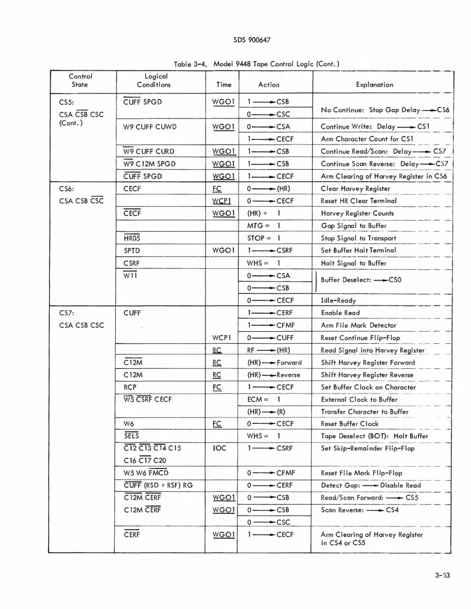
SDS 900647
Table 3-4. Model 9448 Tape Control Logic (Cont.) -, .. _-Control Logical State Conditions Time Action Explanation
-.-. --CS5: CUFF SPGD WG01 1---CSB
Stop Gap Delay --cs6l --- O--CSC No Continue:
CSA CSB esc -- .--
(Cont. ) W9 CUFF CUWD WG01 O--CSA Continue Write: Delay~CS1 ---
1--CECF Arm Character Count for CS 1 ._" - .. -
W9 CUFF CURD WG01 1 CSB Continue Read/Scan: Delay- CS7 --- ---- --
W9 C12M SPGD WG01 1 .. CSB Continue Scan Reverse: Delay--CS7 -- --
CUFF SPGD WGOl l--CECF Arm Clearing of Harvey Register in C56 -. CS6: CECF FC
I
O--(HR) C lear Harvey Register --------
CSA CSB CSC YYQl O---CECF Reset HR Clear Terminal ----- ------- --
CECF WGOl (HR) + 1 Harvey Register Counts --- ---
MTG= 1 Gap Signal to Buffer _.- .. ~-- ------_.. -- -".- -
HR05 STOP = 1 Stop Signal to Transport -- -.
WG01! SPTD l--CSRF Set Buffer HaltTerminal _ .. _------ -'--- ---j
CSRF WHS= 1 Halt Signal to Buffer
~ -Wll O--CSA I Buffer Deselect: -eso I O--CSB I --
O--CECF Idle-Ready -- --CS7: CUFF 1 • CERF Enable Read
----CSA CSB CSC 1--CFMF Arm File Mark Detector
------ --WCPl 0 • CUFF Reset Continue FI ip-Flop
-- -_._--" -- -- ---
~ RF-(HR) Read SL~l~<:J.Il.r:!!~l:!ar\f~_~~ter -----C12M RC (HR) --- Forward Shift Harvey Register Forward
-- ---- - ---- --- -C12M RC (HR) --Reverse Shift Harvey Register Reverse
---. -----,- -- -RCP FC 1---CECF Set Buffer Clock on Character
----- ---"" -- --W5 CSRF CECF ECM= 1 External Clock to Buffer
---.-(HR)---(R) Transfer Character to Buffer
--_.- .. _-_. --
W6 FC O--CECF Reset Buffer Clock ------ --- -- -
SELS WHS= 1 Tape Desel ect (BOT): Halt Buffer -------------- ---
C12 C13 C14 C15 IOC l---CSRF Set Skip-Remainder Flip-Flop -
C 16 C17 C20 - ------"--,- _. --_."------- --
W5W6 FMCD O---CFMF Reset File Mark Flip-Flop ---------- --- --
CUFF (RSD + RSF) RG O---CERF Detect Gap: - Disable Read ---- -
C 12M CERF WGOl O-CSB Read/Scan Forward: - CS5 ---------- --_. -- -
C 12M CERF WG01 O---CSB Scan Reverse: - CS4
O-CSC --- -- ----
CERF WG01 l-CECF Arm Clearing of Harvey Register in CS4 or CS5
3-53

Table 3-5. Tape Transport Unit Logic Equations
F unction I Equation
AANS
AUT
BOTS
BRKl
BRK2
BTL
sCHSB
rCHSB
DATA
EOTS
sEOTl
rEOTl
sEOT2
rEOT2
ETLl
ETL2
FWDl
FWD2
sK 1
rK 1
sK2
rK2
LWDl
LWNl
LWD2
LWN2
RDAl
RDA2
3-54
LTDl + LTNl + LTD2 + LTN2
K2D AUTO Switch
BOTl + BOT2
FWDl REVl REWl
FWD2 REV2 REW2
BOT
(LTNl + LTN2) (S12T + Tl2S)
(LTDl + LTD2) (S l2T + T12S)
SEll + SEL2
EOTl + EOT2
SBOTl ETTl TSB 1
TSB 1 En 1 + STOP Button + K2D
SBOT2 ETT2 TSB2
TSB2 ETT2 + STOP Button + K2D
EOTl
EOT2
TSA 1 TSB 1
TSA2 TSB2
REW
REW
BOT EOR RESET Button
BOT + EOR
SEll CHSB WRTS WEDl
SEL 1 CHSB WRTS WEN 1
SEL2 CHSB WRTS WED2
SEL2 CHSB WRTS WEN2
TSB 1 AUTl RDYl
TSB2 AUT2 RDY2
SDS 900647
Table 3-5. Tape Transport Unit Logic Equations (Cont. )
Function I Equation
RDAS
RDDl
RDD2
RDNl
RDN2
RDYS
RDYl
RDY2
REVl
REV2
DATA (LRDl + LRNl + LRD2 + LRN2)
SEL 1 CHSB AUTl
SEL2 CHSB AUT2
SEL 1 CHSB
SEL2 CHSB
TSAl RDAl + TSA2 RDA2 -- --
AUTl (LTNl + LTD1) (BTSl + BOT1) -- --
AUT2 (LTN2 + LTD2) (BTS2 + BOT2)
TSAl TSBl
TSA2 TSB2
REWl TSA 1 TSB 1
REW2
SELS
SELl
SEL2
sTSAl
rTSAl
sTSA2
rTSA2
sTSB 1
rTSB 1
sTSB2
rTSB2
TSA2 TSB2
SEL 1 + SEL2
AUTl (TSA 1 TSB 1 + TSA 1 TSB 1
+ SEL 1 STOP)
AUT2 (TSA2 TSB2 + TSA2 TSB2
+ SEL2 STOP)
(LTNl FPDl + LTDl FPNl
+ LTN2 FPD2 + LTD2 FPN2) K2C
RDYl (BOTl REWM + Tl2S)
+ MAN 1 K2D (FWDl EOTl + REW1)
TSB 1 SEL 1 STOP + MAN 1 (TSB 1 EOTl
+ REV1) + STOP Button + K2D
+ BOTl BOTl
RDY2 (BOT2 REWM + Tl2S)
+ MAN2 K2D (FWD2 EOT2 + REW2)
TSB2 SEL2 STOP + MAN2 (TSB2 EOT2
+ REV2) + STOP Button + K2D
+ BOT2 BOT2
RDYl BOTl (REWM + S12T)
+ K2D MAN 1 (REV 1 + REW1)
TSA 1 SEll STOP + MAN 1 FWDl
+ K2D + STOP Button' + BOT 1 BOT 1
RDY2 BOT2 (REWM + S12T)
+ K2D MAN2 (REV2 + REW2)
TSA2 SEL2 STOP + MAN2 FWD2
+ K2D + STOP Button + BOT 1 BOTl
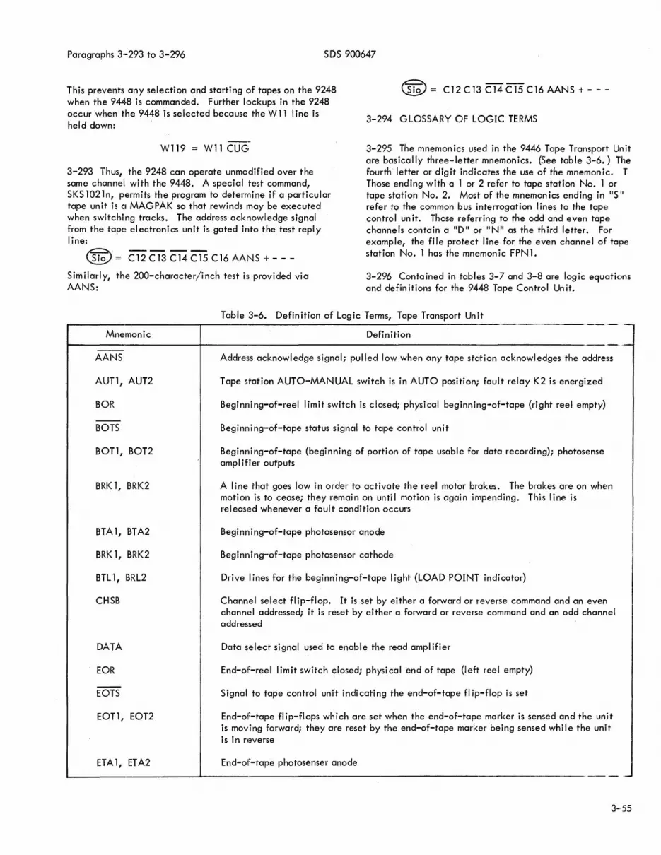
Paragraphs 3·-293 to 3-296 sos 900647
This prevents any selection and starting of tapes on the 9248 when the 9448 is commanded. Further lockups in the 9248 occur when the 9448 is selected because the W 11 I ine is held down:
@ = C 12 C 13 C 14 C 15 C 16 AAN S + - - -
3-294 GLOSSARY OF LOGIC TERMS
Wl19 = Wll CUGi
3-293 Thus, the 9248 can operate unmodified over the same channel with the 9448. A special test command,
3-295 The mnemonics used in the 9446 Tape Transport Unit are basically three-letter mnemonics. (See table 3-6.) The fourth letter or digit indicates the use of the mnemonic. T Those ending with a 1 or 2 refer to tape station No. 1 or tape station No.2. Most of the mnemon ics ending in liS" refer to the common bus interrogation lines to the tape control un it. Those referring to the odd and even tape channels contain a "0" or "N" as the third letter. For example, the file protect line for the even channel of tape stat ion No. 1 has the mnemon i c F PN 1.
SKS 1021n, permits the program to determine if a particular tape unit is a MAGPAK so that rewinds may be executed when switching tracks. The address acknowledge signal from the tape electronics unit is gated into the test reply line:
@= C12 C13 C14 C15 C16 AANS + - -
Similarly, the 200-character/inch test is provided via AANS:
3-296 Contained in tables 3-7 and 3-8 are logic equations and definitions for the 9448 Tape Control Unit.
Mnemonic
AANS
AUTl, AUT2
BaR
BaTS
BOTl, BOT2
BRK 1, BRK2
BTA1, BTA2
BRK 1, BRK2
BTLl, BRL2
CHSB
DATA
EaR
EaTS
EOT1, EOT2
ETA 1, ETA2
Table 3-6. Definition of Logic Terms, Tape Transport Unit
Definition
Address acknowledge signal; pulled low when any tape station acknowledges the address
Tape station AUTO-MANUAL switch is in AUTO position; fault relay K2 is energized
Beginning-of-reel limit switch is closed; physical beginning-of-tape (right reel empty)
Beginning-of-tape status signal to tape control unit
Beginning-of-tape (beginning of portion of tape usable for data recording); photosense ampl ifier outputs
A line that goes low in order to activate the reel motor brakes. The brakes are on when motion is to cease; they remain on until motion is again impending. This line is released whenever a fault condition occurs
Beginning-of-tape photosensor anode
Beginning-of-tape photosensor cathode
Drive lines for the beginning-of-tape light (LOAD POINT indicator)
Channel select flip-flop. It is set by either a forward or reverse command and an even channel addressed; it is reset by either a forward or reverse command and an odd channel addressed
Data select signal used to enable the read amplifier
End-of-reel I imit switch closed; physi cal end of tape (left reel empty)
Signal to tape control unit indi cating the end-of-tape fl ip-flop is set
End-of-tape flip-flops which are set when the end-of-tape marker is sensed and the unit is moving forward; they are reset by the end-of-tape marker being sensed while the unit is in reverse
End-of-tape photosenser anode
3-55

3-56
Mnemonic
ETK 1, ETK2
ETL 1, ETL2
ETT1, ETT2
FPD1, FPD2
FPN\ FPN2
FWD1, FWD2
K1
K2
LLTO-LLT7
LRD1, LRD2
LRN1, LRN2
LTD1, LTD2
LTN1, LTN2
LWD1, LWD2
LWN1, LWN2
MAN1, MAN2
PLP1, PLP2
RDA 1, RDA2
RDAS
RDD1, RDD2
RDK
RDLl, RLD2
RDN1, RDN2
RDR,
RDYS
RDY1, RDY2
SDS 900647
Table 3-6. Definition of Logic Terms, Tape Transport Unit (Cont.)
Definition
End-of-tape photosensor cathode
Drive lines for END-OF-TAPE lights
End-of-tape photosense ampl ifier outputs used to set EOTl or EOT2
File protect odd line from file protect switch
File protect even I ine from file protect switch
A line that is pulled low to energize the forward solenoid (which operates the forward pressure roller)
Rewind relay (when energized, tape rewinds)
Fault relay (when energized, no fault condition exists)
Unit select lines from the tape control unit
Logic read odd preamplifiers
Logic read even preampl ifiers
Logic tape odd (ground for the active unit select lines)
Logic tape even (ground for the active unit select lines)
Logic write odd drivers
Logi c write even drivers
Tape station is in manual mode of operation (AUTO-MANUAL switch is in MANUAL)
Photosense lamp suppl y lines
Read data si gnals
Output of the read amp I ifier after shaping
Read data odd (gated with the lines from the read heads)
Read odd wire from the read head (black)
Drive I ines for READY indicators
Read data even (gated with the I ines from the read heads)
Read odd wire from the read head (red)
Select ready signal to the tape control unit which indicates there is no motion, the unit is in automatic, there is no stop delay, and the K2 relay is energized
Tape station ready signal indicating the unit will accept a command if addressed

SDS 900647
Table 3-6. Definition of Logic Terms, Tape Transport Unit (Cont.)
~ __ M_n_e_m_o_n._ic _____ --1-_____ ...;.. __________ D_e_f_i_n_it_io_n ______________________ J REV1, REV2
REW1, REW2
REWM
RNG
RNU
RTRN
SEL 1, SEL2
SELS
STOP
S12T
TFPS
TSA 1, TSA2
TSB 1, TSB2
Tl2S
WED1, WED2
WEN1, WEN2
WDAS
WDG1, WDG2
WDW1, WDW2
WNB1, WNB2
WNY1, WNY2
WRTS
A I ine from a relay driver to the reverse solenoid which is pulled low to operate the reverse pressure roller
A line which is pulled low to energize the rewind relay, K 1
Rewind command from the tape control unit; it goes to all tape stations on the line, but onl y the tape station that is addressed wi II interpret and operate on the command
Read even wire from the read head (gray)
Read even wire from the read head (bl ue)
Return line for the AUTO-MANUAL switch
Signal indicating that a tape station is in automatic, has been addressed, tape is in motion (but not rewinding), and data can be expected to be either read or written on that particular tape station
Select signal to the tape control unit indicating that a tape station has been selected and is expected to transmit or receive data
Signal from the STOP switch which is used to reset the TSA and TSB flip-flops
Reverse start command si gnal to all tape stations; onl y the tape station addressed wi II respond
Tape file protect signal to the tape control unit which (when pulled down) indicates that a channel which has been selected is file protected
Tape station IIA II fl ip-flop used to control tape motion; it is true for either forward or rewind operation
Tape station IIBII fl ip-flop 'used to control tape motion; it is true for either rewind or reverse operation
Forward start command signal to all tape stations; only the tape station addressed wi II respond
Write enable odd signal derived from the file protect switch
Write enable even si gnal derived from the fi Ie protect switch
Write data signal from the tape control unit
Write odd wire from the write head (green)
Write odd wire from the write head (white)
Write even wire from the write head (brown)
Write Elven wire from the write head (yellow)
Write select control signal from the tape control unit
L-________________ ----L---------~---------------------------------------------------------.-
3-57
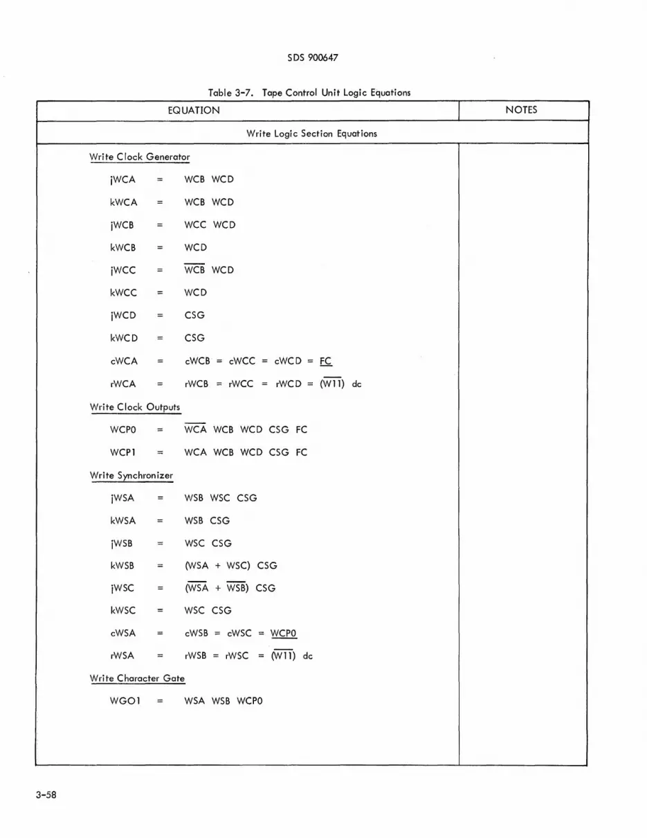
SDS 900647
Table 3-7. Tape Control Unit Logic Equations
EQUATION NOTES
Write Logic Section Equations
Write C I oc k Generator
jWCA = WCB WCD
kWCA = WCB WCD
jWCB = WCC WCD
kWCB = WCD
jWCC = WCB WCD
kWCC = WCD
jWCD = CSG
kWCD = CSG
cWCA = cWCB = cWCC = cWCD = FC
rWCA = rWCB = rWCC = rWCD = (Wll) dc
Write Clock Outputs
--WCPO = WCA WCB WCD CSG FC
WCPl ::; WCA WCB WCD CSG FC
Write Synchronizer
jWSA = WSB WSC CSG
kWSA = WSB CSG
jWSB = WSC CSG
kWSB = (WSA + WSC) CSG
jWSC = (WSA + WSB) CSG
kWSC = WSC CSG
cWSA = cWSB = cWSC = WCPO
rWSA = rWSB = rWSC = (Wll) dc
Write Character Gate
WGOl = WSA WSB WCPO
3-58

SDS 900647
Table 3-7. Tape Control Unit Logic Equations (Cont.)
EQUATION NOTES ~------------------________ • __________________________________ L-_______________________ __
Write Logic Section Equations (Cont. )
Write Flip-Flop
jWF kWF == W9 CSG
cWF
+ CSl CECF WSA WSB WCPO
+ CS2 HROO WCPO
+ CS3 CECF WSA WSB WSC WCPO
rWF (Wll) dc
Read Logi c Secti on Equati ons
Read Signal Standardizer
--dRSFl = RDAS TEST
+ WDAS TEST
dRSF2 = RSFl
cRSFl = cRSF2 = FC
rRSF 1 = rRSF2 = STRT
gRSFl = gRSF2 = CERF
Standardized Read Pulses
RSF3
~ead Flip-Flop
jRF
kRF
cRF
Read Clock
RC
Read Gap
RG
=
=
=
=
=
RSF 1 RSF2 + RSF 1 RSF2
RDA RSF3
RDA RSF3
FC
RSF3 RDA FC
RSF3 RDA RDB ROC RDD
+ RSF3 RDA RDB (RDC + RDD)
,., Sync
Preamble
Write
Postamble
Normal
Back-to-Back Test
Reference Clock
Initial ize
Enable
Arm
Reset for Zero
Late Transition
Earl y Transition
L---__________________ ---' _______________________ ...l-______________ , __ _
3-59
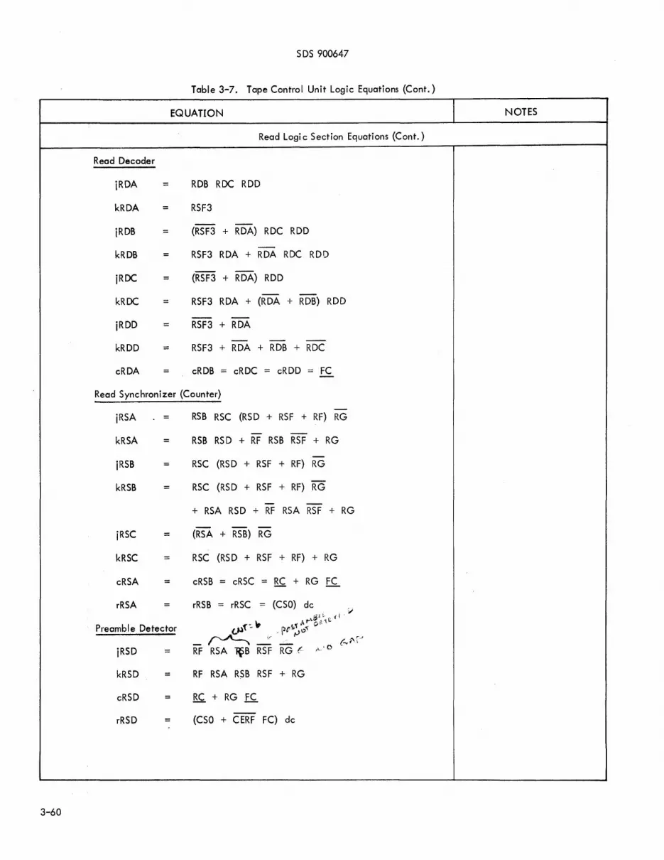
3-60
SDS 900647
Table 3-7. Tape Control Unit Logic Equations (Cont.)
EQUATION
Read Logi c Section Equations (Cont.)
Read Decoder
jRDA = RDB RDC RDD
kRDA = RSF3
-jRDB = (RSF3 + RDA) RDC RDD
-kRDB = RSF3 RDA + RDA RDC RDD
jRDC = (RSF3 + RDA) RDD
-kRDC = RSF3 RDA + (RDA + RDB) RDD
- -jRDD = RSF3 + RDA
- - -kRDD = RSF3 + RDA + RDB + RDC
cRDA = cRDB = cRDC = cRDD = FC -Read Synchronizer (Counter)
jRSA
kRSA
jRSB
kRSB
jRSC
kRSC
cRSA
rRSA
=
=
=
=
Preamble Detector
jRSD =
kRSD =
cRSD =
rRSD =
RSB RSC (RS D + RSF + RF) RG
RSB RSD + RF RSB RSF + RG
RSC (RSD + RSF + RF) RG
RSC (RSD + RSF + RF) RG
+ RSA RSD + RF RSA RSF + RG
(RSA + RSB) RG
RSC (RSD + RSF + RF) + RG
cRSB = cRSC = RC + RG K
rRSB = rRSC = (CSO) dc
RF RSA R~B RSF + RG
RC + RG FC
(CSO + C ERF FC) dc
NOTES

SDS 900647
Table 3-7. Tape Control Unit Logic Equations (Cont.)
Parity Error Detector
jRSE =
kRSE =
cRSE =
rRSE =
gRSE =
Postambl e Detector
jRSF =
kRSF =
cRSF =
rRSF =
gRSF =
Read Character Pulse
RCP
Read Error Signal
RES
EQUATION
Read Logic Section Equations (Cont.)
RSD RF RG
CERF RF RSD
RC + RG FC
RF RSD CERF
RC + RG FC
(STRT + CERF FC) dc
CERF
-RSA RSB RSD (RSF + RF) RC
RG RSD FC
-+ RSE RSA RSB RSC RSF
+ RSA RSB RSD RSF
. Harvey Register Section Equations
Harvey Register Control
Shift Forward Gate
5FG CS27 C 12M CECF
5hift Reverse Gate
5RG C527 C 12M CECF
5hift Parall el Gate
5PG CS2 CECF
NOTES
Gap in Data (01-32-31)
Parity Error (01-32-22)
Premature Postamb I e (01-32-18)
C52 + C57
C52 + C57
C52
3-61

SDS 900647
Table 3-7. Tape Control Unit Logic Equations (Cont.)
EQUATION
Harvey Register Section Equations (Cont.)
Harvey Register Control (Cont.)
Count Binary Gate
CBG CSO
+ (CS4 + CS56) CECF
Serial Shift Pulse
SSP CS2 WCPO
+ CS7 RC
Shift Parallel Pulse
SPP CSO CS7 C ECF FC
Harvey Register Gate
-HRG SFG SRG SPG CBG
Harvey Register Inputs J.J....~ ... --.,~ --
dHROO = SFG HROl + SRG RF + SPG RP + CBG HROO
dHROl = SFG HR02 + SRG HROO + SPG R 1 + CBG HROl
dHR02 = SFG HR03 + SRG HROl + SPG R2 + CBG HR02
dHR03 = SFG HR04 + SRG HR02 + SPG R3 + CBG HR03
dHR04 = SFG HR05 + SRG HR03 + SPG R4 + CBG HR04
dHR05 = SFG HR06 + SRG HR04 + SPG R5 + CBG HR05
dHR06 = SFG ;HRIN'~ SRG HR05 + SPG R6 + CBG HR06
HRIN = Vf! RF + W9 HROqit, ~ ~J;1 ~ ';Ae~Q t\~, r5:' r
Harvey Register Clocks " .~~.
cHROO = SSP + SPP + CBG WGOl
cHROl = SSP + SPP + CBG HROO
cHR02 = SSP + SPP + CBG HROl
cHR03 = SSP + SPP + CBG HR02
cHR04 = SSP + SPP + CBG HR03
3-62
NOTES
CSO
CS4, 5, 6
Write
Read
Output from Buffer and HR Clearing
Inverter Control

SDS 900647
Table 3-7. Tape Control Unit LOQic Equations (Cont.)
EQUATION
Harvey Register Section Equations (Cont.)
Harvey Register Clocks (Cont.)
cHR05
cHR06
SSP + SPP + CBG HR04
SSP + Spp + CBG HR05
rHROO rHROl = - - - = rHR06 = 0Nll) de
~arvey Register Outputs
Delay Definitions
STGD = HR05 HR04 HR02 HROO WG01 STAtl. r 6 WTRD = HR05 HR04 HR01 HROO WG01 LJRITE. TO ~
SPGp = HR05 HR02 HROl WG01 Sro p 6AP Del-
SPTD = HR05 HR03 HR02 HROO WG01 S"'oP 'APE t,:
CUWD = HR06 HR04 HR03 HR01 WG01 c.c AJ n l\t LJ €. WI(.
IHGD = HR06 HR03 HR01 HROO WGOl T~ rE'I' t-\ EA"C (
NOTES
~ fP .l)fj 1:+ '\ - 6{,r"~4o-'..\-(."'-
RF'~D U E~/'.Ir'l - 34.1~ De ~ 1. 41
~~, - "Lip /Yl'lA~'-" ".
f-lA"f - ~ C". "1.· ,'", \.~.L L~ c,..
frC~- 'De~1 - to C>. r~/''Y'''''f ~ A ~ ,
~\.~fArC:'O 'v f:l,.A" - .: 0."--: ('1 ,\" U \..4.
CURD = HR06 HR05 HR04 HR03 WG01 ~JJ't" /tUt"tE:- K'ti:A~ D ,,-,1-1 '1 ~7 s. rs''J \. '.' ,-
File Mark Detect
-- --FMCD = HROO HR01 HR02 HR03 HR04 HRQ5 HR06 Jt'
( 1 , 8 " f" ,r·'
Control Logi c Section Equations r------------------------------------------------------~----------------------
Control State Counter
jCSA
kCSA
JCSB
CSO IHGD
+ CSO W9 C12M
+ CS3 CECF
CS5 W9 CUFF CUWD
CSO IHGD
+ CSO W9 C12M
+ CS1 CECF
+ CS4 WlO IHGD
+ CS5 SPGD CUFF
+ CS5 W9 C12M SPGD
+ CS5 CUFF CURD
Read/Scan Forward: CSO - CS7
Scan Reverse: CSO-CS7
Write/Erase: CS3-CS4,5
Write Continue: CS5-CS1
Read/Scan Forward: CSO --CS7
Scan Reverse:
Write/Erase:
Erase Reverse:
Non Continue:
Scan Reverse:
Read Conti nue:
CSO-CS7
CS1-CS2
CS4--CS6
CS5-CS6
CS5-CS7
CS5-CS7
3-63
·fJl (' It 4"

SDS 900647
Table 3-7. Tape Control Unit Logic Equations (Cont.)
EQUATION NOTES
Control Logic Section Equations (Cont.)
Control State Counter (Cont.)
--kCSS = CS3 CECF Write/Erase: C53-CS4,5
--+ CS7 CERF Read/Scan: C57---C54,5
jCSC = CSO W9 5TGD Write/Erase: C50---CSl
-+ CSO W9 C12M Scan Reverse: C50-CS7
+ CSO IHGD Read/Scan Forward: CSO -CS7
+ CS2 W5 CUFF Write/Erase: CS2 -CS3
+ CS2 W5 CFMF Write File Mark: CS2 -CS3
-- --+ CS4 W9 W10 CERF WTRD Write: CS4 -CS5
-+ C54 W9 WTRD Scan Reverse: CS4 -CS5
--+ CS4 WlO IHGD Write: CS4---C55
kCSC = CS1 CECF Write/Erase: CS1---CS2
- --+ CS3 WlO CECF Write: C53---CS4
--+ CS3 C12M CECF Erase Reverse: CS3-CS4
--+ CS5 SPGD CUFF Non Continue: CS5-CS6
--+ CS7 C12M CERF Scan Reverse: CS7--CS4
---rCSA = rCSS = rCSC = (W11 STRT) de Any State CSO
cCSA = cCSS = cCSC = WG01 C haracter-Time Clock
Control State Definitions
- --CSO = CSA CSB CSC Start
-CS1 = CSA CSB CSC Preamble
CS2 = CSA CSS CSC Write
CS3 = CSA CSB CSC Postamble
- -CS4 = CSA CSB CSC Interhead
-CS5 = CSA CSB CSC Gap
-CS6 = CSA CSB CSC Stop
CS7 = CSA CSB CSC Read
3-64

SDS 900647
Table 3-7. Tape Control Unit Logic Equations (Cont.)
EQUATION I NOTES
Control Logic Section Equations (Cont.)
Control State Definitions (Cont.)
CS13 CSA CSC Preamble/Postamble (CS 1 + CS3)
CS27 CS2 + CS7
CS56 CS5 + CS6
Con'trol Select Gate
CSG CSA + CSB + CSC + CECF
External Clock Flip-Flop
IJ}.CECF CSO STRT SELS H"~
Write/Read
Gap/Stop
Out of Idle-Ready
Depart I dl e-Ready
+ csq WGOl Preamble/Postamble Character Count
{lJ<CECF
+ (S2 (CUFF + CFMF) WGOl
+ (S4 CERF WTRD W9 WlO C12M SELS }
+ CS4 IHGD
+ CS5 CUFF SPGD
+ (S5 W9 CUFF CUWD
+ CS7 RCP
+ CS7 CERF WG01
CSO W9 C12M WG01
+ CSO IHGD
Write/Erase: Clock to Buffer
Arm HR Clearing in CS5, 6
Arm HR Clearing in CS6
Arm H R C I eari ng inC S 1
Read/Scan: C lock to Buffer
Arm HR Clearing in CS4, 5
Scan Reverse: Reset Clock
Read/Scan Forward: Reset Clock
+ CS13 WG01 Preamble/Postamble Character Count
+ (CS4 + CS5 + CS6) WCP 1 HR Clearing Complete
+ CS27 W6 Reset Clock to Buffer
sCECF (CS 1 W 1 0 ~ 12M RG + Fe CS4 RSA RSB C 12M) dc Scan/Erase over Gap
----rCECF (W11 STRT) dc Hold in Idle-Ready
cCECF .E£. Reference Clock
Control Logic DC Flip-Flops
Tape Reverse Monitor FF
sC12M
rC12M
STRT C 12
W11
Set for Reverse
C lear Reverse
3-65

3-66
SDS 900647
Table 3-7. Tape Control Unit Logic Equations (Cont.)
EQUATION
Control Logic Section Equations (Cont.)
Control Logic DC Flip-Flops (Cont.)
Erase Tape FF
sCETF
rCETF
Enable Read FF
sCERF
rCERF
sCUFF
rCUFF
CSO W9 Wl1 WCPl
+ CS3 CECF WSB WCP1
CS1 W10 WSA WSC WCP1
CS13
+ CS7 CUFF
CSA CUFF (RSD + RSF) RG FC
+ Wll
CS2 W5 WSB WCP1
+ CS5 STRT
+ Wll
CS13
+ CS7 WCP1
Skip Remainder FF
sCSRF
rCSRF
File Mark FF
sCFMF
rCFMF
CS2 CUFF WG01
+ CS6 SPTD
+ CS7 CNTL (C12 C13 C14 C15 C16)
CSB WCP1
+ STRT Q2 SELS
CS2 W5 CSRF WSA WCP1
+ CS7 CUFF
(513
+ CS7 W5 W6 FMCD
+ RSD RG FC
+ STRT
NOTES
Write/Erase: Begin Erase
Terminate Postamble
Commence Preamble
Write/Erase: Enable Read
Read: Enable Read
CS4, 5, 6, 7: Disable on Gap
Disable Read
Normal Write Detect
Remember Continue Command
Arm for CERF, CFMF in CS7
Write: Reset for CS2, CS5
Complete Setting of CERF, CFMF
Write: Count First Character
Remember Buffer Halt in CSO
Disable Clocks to Buffer
C SO, 1, 4, 5: Reset for CS2, 6, 7
Detect 9248 Selection
Write File Mark: Second Character
Read Fi Ie Mark: Arm
Write: Reset for CS2
Read File Mark: Detect
Defeat F i I e Mark if Gap in Record
Reset if 9248 Se I ected

SDS 900647
. Table 3-7. Tape Control Unit Logic Equations (Cont.)
EQUATION I NOTES -"
Control Tape Logi c Equations --. Logical Tape Transport Address
- .- -LLTO = C21 C22 C23
- .-LLT1 = C21 C22 C23
- -I LLT2 = C21 C22 C23
- j LLT3 = C21 C22 C23 i
1 .- - I LLT4 = C21 C22 C23
.-
I LLT5 = C21 C22 C23
-LLT6 = C21 C22 C23 i LLT7 = C21 C22 C23 l
I
?tart/Control Signals ! 1
-- I STRT = Buc C 17 C20 Buffer Unit EOM
--CNTL = Ioc C 17 C20 I/O Control EOM
Tape Motion Control Signals
-Tl2S = STRT C12 Q2 Start Forward
S12T = STRT C12 Q2 Start Reverse
---REWM = CNTL C12 C16 TEST Start Rewind
-- -- --STOP = HR05 CS6 + Wll STRT Stop Forward/Reverse
Wri te Data/Control
WRTS = W9 SELS Write Control
--WDAS = CETF WF Write Data
Control-Computer Logi c Equations
Character Transfer to Buffer
(Jl!Jj) ---= CS7 HR01
OWV ---= CS7 HR02
Q~D ---= CS7 HR03
~ ---= CS7 HR04
(zW§) ---= CS7 HR05
~ ---= CS7 HR06
<1YiV ---= CS7 HROO -
3-67

3-68
C lock To Buffer
@ = Halt to Buffer
Whs =
SDS 900647
Table 3-7. Tape Control Unit Logic Equations (Cont.)
EQUATION
Control-Computer Logic Equations (Cont.)
CS27 CERF CSRF CECF + ECM9
CS6 CSRF + CSO CS56 SELS TEST
+ SELS AANS Q2 STRT + WHS9
Magneti c Tape Gap to Buffer
~ = CS56 CUFF + MTG9
Error Si9nal to Buffer
@ = RES + SELS WES9
Skip Logic
@ = C17 + C20
+ C15 C16 CSO RDYS
-+ C12 C 16 TFPS
+ C 13 C 16 BOTS
-+ C14 C16 EOTS
---+ C12 C13 C14 C15 C16 AANS
- - -- --+ C12 C13 C14 C15 CS5 CUFF CFMF
--+ C12 C13 C14 C15 C16 CUG CFMF
-I- C12 C13 C14 C15 C16 CUG SI09
- - - --+ C12 C13 C14 C15 C16 AANS
Auxiliary-Control Logic Equations for 9248
Control Gate
CUG = CSA + CSB + CSC + CECF + CSRF
Interposed Terms
C179 = 1
C209 = 1
BUC9 = STRT + CS7
IOC9 = CNTL - --
Q29 = Q2 CUG --
Wl19 = W11 CUG
NOTES
Magnetic Tape Inquiry
Control/T ape Ready
Tape File Protect
Beginning of Tape
End of Tape
Tape Density 200 BPI
Control Gap
9448 Fi Ie Mark
9248 Responses
MAGPAK
Indi cate 9448 selected or was last selected
\ Forces 9248 M start true when 9448 selected and reading
Permit Rewind through 9248
Block Q2 to 9248
Block 9248 Selection

SDS 900647
Table 3--8. Definition of Logic Terms, Tape Control Unit
Mnemonic Definition
AANS
BOTS
BUC
BUC9
CBG
CECF
CERF
CETF
CFMF
CNTL
CSA-CSC
CSG
CSRF
CSO-CS7
C50
C51
C52
C53
C54
C55
C56
C57
CS13
C527
CS56
CUFF
Address (lcknowledge signal from 9446 tape unit used to respond to tape density tests
Beginning of tape signal from addressed unit
Buffer unit control signal (Buc) used to strobe EOM commands
Auxiliary BUC to 9248 connector
Count binary gate. Conditions the Harvey register to provide time delays by counting WG01 pulses
External clock flip-flop. Provides Ecw signal to buffer and is time-shared to perform other control functions
Enable read fl ip-floPi also used in gap detector
Erase tape fl ip-flop
File mark flip-flop
Control signal for magnetic tape decoded from computer IOC command
Control state counter
Control selected gate indicating that 9448 has been taken out of idle-ready by an STRT from the computer buffer
Skip remainder flip-floPi time-shared for remembering that the lost command given was to a MAGPAK
Control States:
IDLE-START
PREAMBLE
WRITE
POSTAMBLE
INTERHEAD
GAP
STOP-HALT
READ
Control States CS 1 or CS3. Indicates that preamble or postamble is being written
Control States CS2 or CS7. Indicates that writing or reading of characters is tak ing place
Control States CS5 or CS6. Indicates that a shutdown sequence is in progress
Continue FI ip-Flop
3-69

3-70
Mnemonic
CUG
CURD
CUWD
C12-C23
C12M
ECM
ECW
EOTS
Fe
FMDG
HRG
HROO-HR06
IHGD
10C
IOC9
LLTO-LLT7
MTG
MTG9
02
029
RC
RCP
RDA-RDD
RDAS
RDYS
RES
REWM
RF
RG
R1-R6, RP
RSA-RSC
SDS 900647
Table 3-8. Definition of Logic Terms, Tape Control Unit (Cont.)
Defin ition
Control Unit Gate. Indicates that 9448 is selected or that the 9248 is not selected
Continue Read Delay (75.5 ms)
Continue Write Delay (60.7 ms)
Computer C Register signals used to control 9448
Reverse Mon itor FI ip-Flop. Stores C 12 throughout tape operation
Clock to Computer Buffer (Ecm). For W-Buffer, this term is represented as ECW.
See ECM
End-of- Tape signal from addressed tape unit
Reference Clock. Crystal-controlled oscillator, operating at 126 Kc (12 times the MAGPAK bit-rate)
File Mark Detect Gate
Harvey Register Gate used to qual ify inverter logic
Seven-Stage Harvey Register. Converts serial/parallel and parallel/serial, and provides all MAGPAK timing terms by acting as a binary computer
Interhead Guard De lay (50.7 ms)
Input/Output Control signal (Ioc). Used to strobe EOM commands
Auxiliary 10C to 9248 connector
Logical Tape Unit addresses decoded from C21-C23
Magnetic Tape Gap signal (Mtg) to Computer Buffer
Auxiliary MTG signal from 9248 connector
Computer pulse counter signal
Auxiliary 02 to 9248 connector
Read Clock derived in RDA-RDD, used to strobe RF
Read Character Pulse, derived in RSA-RDS, coincident with every 7th RC signal after character sync is estab I ished
Read Decoder Flip-Flops. Act as variable period binary counter clocked by FC
Read Data Signal from 9246 electronic unit
Ready Signa I from addressed transport
Read Error Signal
Rewind Control signal to addressed transport
Read Flip-Flop. Converts FM signal from tape to serial binary
Read Gap. Indicates gap condition detected by RDA-RDD
Computer Buffer para lie I output signa Is
Read Synchronizer Flip-Flop, used as seven-state binary bit-time counter clocked by RC

Mnemonic
RSD
RSE
RSF
RSF l-RSF2
RSF3
SELS
SFG
SIO
SI09
SPG
SPGD
SPTD
SRG
STGD
STOP
STRT
S12T
TEST
TFPS
Tl2S
WCA-WCD
WCPO
WCP1
WDAS
WES
WF
WG01
WHS
WRTS
WSA-WSC
WTRD
WO
W5
W6
SDS 900647
Table 3-8. Definition of Logic Terms, Tape Control Unit (Cont.)
Definition
Read Synchron izer FI ip-Flop, used to detect preamble and control/character reading
Read Synchronizer Flip-Flop, used to detect serial odd parity errors
Read Synchronizer Flip-Flop, used to detect and confirm the postamble
Read Standardizer Flip-Flops. Act as shift register for RDAS signal clocked by FC
Standardized Read signal transitions formed by gating between RSF 1 and RSF2
Select Signal from 9446, indicating that addressed transport is selected
Shift Forward Gate to Harvey Register
Response from I/O device (Sio) to SKS instructions
Auxiliary SIO signal from 9248 connector
Shift Parallel Gate to Harvey Register
Stop Gap Delay (26.0 mS)i allows time for Continue Flip-Flop, CUFF, to set if continue option is desired
Stop Tape Delay (30.7 mS)i maintains current in write heads until tape stops
Shift Reverse Gate to Harvey Register
Start Gap Delay (36.0 mS)i allows time for tape to start and travel 0.225 inch
Stop signal to 9446 to halt tape motion
Magnetic Tape Start signal decoded from Computer BUC command
Start Tape Motion in Reverse command to addressed transport
Control signal which, when grounded, causes data to be coupled back-to-back, write to read, and prevents tape motion commands
File Protect signal from 9446 indicating switch position on addressed transport.
Start Tape Motion Forward command to addressed transport
Write Clock Generator Flip-Flops, operating as a twelve-state counter clocked by FC
Write Clock Phase Zero, pulse derived in WCA-WCD. Indicates time to write zero transition
Write Clock Phase One, pulse derived in WCA-WCD. Indicates time to write synchrol'l'izing transition
Write Data Signal to selected transport
Error Signal to Computer Buffer (Wes)
Write FI ip-Flop. Converts serial binary to FM recording format
Write Character Pulse derived in WSA-WSC
Halt Si~lnal to Computer Buffer (Whs)
Write Control Signal to 9446
Write Synchronizer operating as a seven-state binary counter clocked by WCPO
Write to Read Delay (34. 7 ms)
W-Buffer Flip-Flop signal in controlling termination of data transfer
W-BuffElr Precess Detector, participates in halt interlock
W-Buffer Flip-Flop signal used to acknowledge Ecw
3··71

SDS 900647
Table 3-8. Definition of Logic Terms, Tape Control Unit (Cont.)
Mnemonic Definition
W9 W-Buffer FI ip-Flop signal indicating an output operation
W10 W-Buffer Flip-Flop signal indicating erase or scan operations
Wll W-Buffer FI ip-Flopdesignates magnetic tape operations
ZW1-Zw6, ZWP Computer Buffer parallel input lines (Zw l-Zw6, Zwp)
3-72

SDS 900647 Paragraphs 4-1 to 4-8
SECTION IV
INSTALLATION AND MAINTENANCE
4-1 IN STALLA TION
4-2 Basically, the Model 9446 Tape Transport Unit can either be installed in a standard 19-inch relay' rack or mounted on a table (such as the SDS Model 92360 Table). The Model 9448 Tape Control Unit is always rack-mounted.
4-3 These units are shipped either mounted in cabinets or packed in individual, custom-built, packing boxes. In either case, both units can be stored, shipped, or handled in any orientation. Normal unpacking procedures for this type of equipment should be followedi packing cases should be opened carefully and their contents examined for damage incurred during shipment. If the units are to be moved or reshipped, packing similar to that in which the units were received wi II be adequate.
4-4 Tables 4-1 and 4-2 list the environmental specifications and power requirements appl icable to installation of a MAGPAK tape system. Refer to section I of this manual for a complete I ist of MAGPAK specifications. Figures 4-1, 4-2, and 4-3 show the dimensions for the Model 9446 Tape Transport Unit, Model 9402 Dust Cover Housing, and Model 92360 Table, respectively. Refer also to the installation drawings incl uded in section V of this manual.
Table 4-1. MAGPAK Environmental Specifications
Item Spec ifi cation
Operating Temperatures 100
C-400
C (500
F-104°F)
Operating Humidity 20% - 80% RH
Heat Dissipation
9446 900 BTU per hour
9448 450 BTU per hour
Weight
9446 75 Ib (without dust cover)
9448 751b
9402 Dust Cover 251b
92360 Table 651b
Recommended Access 3 ft in front and rear of Area table or cabinet
-
Table 4-2. MAGPAK Power Requirements - ,-
Item Specification
Model 9446 Model 9448
Power Requirements
115 vac ± 10%, 60 cps ±3 cps 2.0 amps
+50 vdc 0.4 amp
+f5 vdc 1. 0 amp 3.4 amps
+ 8 vdc 1.6 amps 1.6 amps
-25 vdc 0.2 amp 0.4 amp
Recommended AC 115 vac, 5 amps Service per Model 9446
AC Service Receptacle Hubbell type 5262 FE polarized, or equivalent
Power Cable Lengths AC: 8ft
DC: 20 ft (std) DC: 5 ft 5 or 10ft (optional)
0 ___ 0_
4-5 INSTALLATION PROCEDURE
4-6 Model 9446
4-7 Rack-Mounted. Mount the 9446 assembly in the 19-i nch rack with the hardware provided. Adapters are avai lable for 24-inch rack mounting. Cable lengths and interconnection requirements must be considered when determining the location of the 9446 assembly.
4-8 Table-Mounted. When the tape transport unit is mounted on a table top, the unit must be enclosed in a Model 9402 Dust Cover Housing. Since the dust cover contains a fan in the base for air circulation, the rubber feet on the base should not be removed. If they are, a hole must be cut in the table top to provide for air flow.

Paragraphs 4~9 to 4-13 SDS 900647
~ >180 0
/ [1100
minimum ] / SDS 19 inch rack
1~~~---------19 inches----------~.-· ~I
T 10.5 inches
1 0 @ °<If:?OO @ I 0 °-f)°OO @ 0
0 0000 0. @OOOOo
~:/,/ 0 0
T 12 inches
r-A---------'-li 900647B.41
Figure 4-1. Model 9446 Tape Transport Unit Dimensions
4-9 Up to two tape transport units may be counted on each Model 92360 Table. The table has a vertical cable trough in the right-hand rear corner, as shown in figure 4-3. Receptacl~s beneath the table connect ac power to the tape transport units. Line power is connected to the receptacles by a 20-foot-long cable.
4-10 Moqel 9448
4-11 Mount the 9448 assembly in the 19-inch rack with the hardware provided. Adapters are available for 24-inch rack mounting. Cable lengths and interconnection requirements must be considered when determining the location of the 9448 assembly.
4-12 INTERCO"INECTING CABLING
4-13 Interconnecting cabl ing for the MAGPAK Tape System is shown in figure 4-4. Refer to this figure and perform the following steps:
a. Install Cable PI ug Module P82 from left tape station in .location J41 of 9446 Tape Transport Unit electronics (designated chassis 00).
b. Install P82 from right tape station in J42-00. Both P82 cables are 3 feet long. (Note that P82 from either the; left or right tape station can be plugged into either J41 or J42 of the 9446 electronicsi the tape stations
4-2
will perform exactly alike regardless of which position they are plugged in. Usually the tape station cable plug modules are connected as shown in figure 4-4.)
c. Install P84 in J26-00i install P83 in J42 of 9448 Tape Control Unit chassis 03.
d. Install P81 in J44-03i install P80 in magnetic tape control connector of computer I/O buffer. The P80-P81 cable is 5 feet long.
e. If additional 9446 Tape Transport Units are to be operated from the same 9448 Tape Control Unit, install P83 in location J27-00 of the preceding tape transport unit. The P83-P84 cable lengths and part numbers are shown in table 4-3. Any combination of cables may be used, but the total length of all P83-P84 cables must not exceed 47 feet for standard MAGPAK tape systems.
f. If the I/O buffer used has time-sharing capabilities, an SDS Model 9248 Magnetic Tape Control Unit (or equivalent) can be operated from the same buffer channel. For this arrangement, remove Termination Module ZX49 from 9448 Tape Control Unit chassis location J41-03, and install Cable Plug Module P40 from 9248 (or equivalent) unit.
g. Connect 9446 dc power cable wires to appropriate computer power buses as indicated in table 4-3. The wires

SDS 900647
5 6 l 1-7.8 inches .. inches
+A A+
17.5 inch es 13.2 in ches
5.5 in!hes [J ~
A A inches
t + + 1.9 inc
FRONT T --- 16.8 inches 1.9
hes 4.5
inches 19.6 inches -- -
A. 6-32 Thread Rubber Bumper Mounting Hole
B. Air Flow Opening
Dust Cove r Height: 13.5 inches 9006478.42
Figure 4-2. Model 9402 Dust Cover Housing Dimensions (Top View)
r---------------------------------'----------------------1-__ ~---------------------54inches------------------~--1
4.5 3.5
linchesl6 inches inches -----..... ,
: 1 ~ I I ---L
~~::eT::~:~ T o~ ~f::T~~ ;e~ : :: ~ -t-T 1 inch
22 inches
Table Height: 30 inches 9006478.43
Figure 4-3. Model 92360 Table Dimensions (Top View)
4-3

Paragraphs 4-14 to 4-15 SDS 900647
are tagged according to voltage requirements. Cable lengths and part numbers are shown in table 4-4.
h. Connect 9448 dc power cable wires to appropriate computer power buses as indicated in table 4-5. The wires are tagged according to voltage requirements. The cable is 5 feet long.
i. Connect 9446 ac power plug P1 to an ac power source.
Table 4-3. Model 9446 DC Power Cable Connections
Wire No.
1
2
3
4
5
6
7
Computer I/O Buffer
From Model 9446 To Power Supply
TB4-E-1 +50v dc
TB4-E-2 +25v dc
TB4-E-3 -25v dc
TB4-E-4 + 8v dc
TB4-E-5 Ov
TB4-E-6 Ground No. 1
TB4-E-7 Ground No. 2
9448 Tape Control Un it
Chassis 01
Chassis 02
5-foot dc power ~------------------~
cable Chassis 03
\ \
3-foot cable
Table 4-4. Model 9446 DC Power Cables
Length (ft) Part No.
20 (std) 110951
10 113986
5 113839
Table 4-5. Model 9448 DC Power Cable Connections
Wire No. From Model 9448 To Power Supply
1 A03 J45-E-47 +25v dc
2 A03 J45-E-46 -25v dc
3 A03 J45-E-45 + 8v dc
4 A03 J45-E-44 Ov
4-14 INITIAL CHECKOUT
4-15 Initial checkout of the MAGPAK tape system involves checking to see that all electromechanical functions are operable. Final mechanical adjustments of MAGPAK are
9446 Tape Transport Unit
Right Tape Station
Left Tape Station
P1 8-foot ac power cable
3-foot cable
5-, 10-, or 20-foot dc
power cable
5-foot cabl e \
\ 5-, 10-, or 20-foot cable
4-4
I
.. IZX~91 \
\
~ I--_ .... To additional 9446 Tape
Transport Units
:,' '" ~ ..... ' "':' ./ \.~ .. ' _ -. t ~ 1
=)'; -.;,
~
_ I~~ To 9248 Tape System or equivalent 900647B.44
'~WJ' \ - .J ·.~\~Figure 4-4. MAGPAK Interconnecting Cabling
i'y .i 1'" \oil:\ ': 1; ~~"

SDS 900647 Paragraphs 4-16 to 4-29
made at the factory and should not have to be made again unless a part is replaced.
4-16 Initial checkout of MAGPAK is accompl ished as follows: Apply power to the equipment and place the AUTO-MANUAL switch in MANUAL. Before loading tape cartridges on the transports, check to ensure that the capstans are rotating and the tension arms are in the correct position. Check to see that the reel motor hubs rotate when the FORWARD, REVERSE, and REWIND buttons are pressed. Note that right hub will not rotate in rewind. Also check the operation of the indicator lights.
4-17 Next, place tape cartridges on the transports and check to see that the tape is guiding correctly. Then check to determine if the beginning-of-tape and end-oftape signals are working properly.
4-18 Operation of the system in the automati c mode can be checked by executing single-instruction EOM' s for the desired operations, such as Read, Write, Scan, and Rewind. The status I ines can be checked with appropriate SKS instructions, or by maintaining the unit in the addressed state.
4- 19 If any of the above checks are unsatisfactory, perform the adjustment described under paragraph 4-30.
4-20 DIAGNOSTIC AND TEST ROUTINES
4-21 The operating status of the unit can be further checked by running a diagnostic or test routine. The following SDS Program Library routines are avai lable:
a. Multi-Unit Magnetic Tape Exerciser (Catalog No. 044004).
b. 42-Kc Magnetic Tape Test Program, W-Buffer (Catalog No. 074001).
c. 42-Kc Magnetic Tape System Exerciser, W-Buffer (Catalog No. 074003).
4-22 Margin testing can be accomplished with other clock crystals or with an audio oscillator. The standard clock crystal (126 kc) is removed from the CX13 module, which is in location J26, chassis 03 of the tape control unit. Another crystal is plugged in on the module, or the audio osci lIator is connected from 03-J26-E-32 to ground. Frequencies above 135 kc require a jumper from 01-J32-E-27 to ground (on the GK51 module) to defeclt the speed test error. The transports normally operate 01- ± 15% speed variation. This may be tried by writing at 108 kc to 145 kc, and reading at 126 kc.
4-23 MAINTENANCE
4-24 PREVENTIVE MAINTENANCE
4-25 No periodi c I ubri cation of the transports or periodi c replacement of parts is required. However, it is important that the tape and transports be kept clean. The read/write heads and all tape guide surfaces ·should be cleaned with denatured alcohol or a commercial magnetic tape head cleaner at least once per 8-hour shift. Also, when the tape unit is in operation, the front cover door should remain closed.
4-26 Satisfactory performance also requires that SDS tape cartridges be used, since these are controlled to a much higher quality standard thpn are the conventional audiotype cartridges that are commercially available.
4-27 TROUBLESHOOTING
4-28 Table 4-6 lists the most frequent malfunctions encountered in MAGPAK. In order to troubleshoot MAGPAK, of course, the technician must understand how the equipment works (see section III), and must be able to distingUish between normal and abnormal operation. Otherwise he wi II have difficulty defining the problem. Refer to section V of this manual for schematics and to section VI for assembly drawings and parts information.
4-29 Normal signal levels for the MAGPAK Tape System are shown in table 4-7. Other signals in the system are ot normal SDS logic levels; that is, Ov for binary zero, and +8v for binary one.
Table 4-6. MAGPAK Troubleshooting Chart
Symptom Possible Cause Remedy --.. -
l. Power failure No power input. Check power connections (see paragraph 4-12).
Fuse Fl (2 amp) Replace fuse blown. (see schematic).
2. Motion functions BOR or EOR Check tension (forward, reverse, switches open arm position; if rewind) inopera- (occasionally normal, ad just tive; no indicator BOR opens in switches 58 or lights. rewind due to 59 (see para-
the increased graph 4-55). tape tension).
Fault relay K2 Replace K2 (see defective. schemati c)_
- -
45

SDS 900647
Table 4-6. MAGPAK Troubleshooting Chart (Cont.)
Symptom Possible Cause Remedy Symptom Possible Cause Remedy
3. Rewind motion Rewind relay K1 Replace K 1 (see 8. (Cont.) Reel motor Ad just reel motor inoperative; defective. schematic) . brakes out of brake armature other motions ad justment. gap (see para-:-normal. graph 4-46).
4. Capstans do not BOR or EOR Check tension 9. Tape tension in- Reel motor stall Adjust reel motor rotate; RESET switches open. arm position; if correct; rewind torque out of stall torque (see !:"utton has been normal, adjust time too slow. adjustment. paragraph 4-50). pushed. switches 58 or
59 (see para- Ree I brakes out Adjust reel motor graph 4-55). of ad justment. brake armature
gap (see para-Fault relay K2 Replace K2 (see graph 4-46). defective. schematic) .
10. Incorrect rewind Right reel motor Adjust right reel 5. Tape guides im- Cartridge loaded Reload cartridge; speed; tape torque out of motor torque (see
properly; tape incorrectly. check cartridge passes BOT adjustment. paragraph 4-52). binds; tape fi t agai nst spri ng marker on re-breab; tape clips and posi- wind. winds' unevenly; tioning pins (see tape spi lis out paragraphs 2-29 11. Tension arm Dashpot out of Adjust dashpot of reel. and 4-65). osc i Ilates. adjustment. (see paragraph
4-60).
Tension arm pins Ad just tension arm 12. Tape hangs up Tape tension arm Adjust retrac-
out of alignment. pins (see para-on tension arm retraction mech- tion mechanism
graph 4-62). pins when cart- anism out of (see paragraph ridge is loaded. adjustment. 4-57).
6. Oxide Worn read/write Replace read/ accumulates. head. head (see
13. BOT or EOT Photosense am- Adjust HX48 schematic) . (Note: Read/
signal inoper- pi ifi er out of (see paragraph
write heads are ative; BOT or ad j ustm ent . 4-34).
sometimes EOT signals
scratched by triggered in-
careless removal correctly. Photosense head Replace lamp
and replacement lamp defective. D56. Readjust
of cross-talk HX48 (see para-
shields.) graph 4-34).
14. Pari ty error. T ape damaged Replace tape
Rough surface in Replace defective or worn. cartridge.
tape guide path. part. Read/write head Replace read/ defective. wri te head (see
7. Tape :move- Capstan/pressure- Ad just capstan/ schematic) . ment erratic. ro II er force pressure -ro II er
incorrect. force (see para-graph 4-43).
8. Tape start -stop Capstan/pressure- Adjust capstan/ 15. Read error. Data amp I ifi er Adjust HX29 times irregular. roller gap pressure-roller level control (see paragraph
incorrect. (see paragraph out of 4-31) . 4-41). ad j ustme nt .
4-6

SDS 900647 Paragraphs 4-46 to 4-51
i. Tighten lower screw on solenoid mounting bracket. Be careful to ensure that solenoid does not move as screw is tightened.
j. Tighten upper screw on solenoid mounting bracket and remove thickness gauge.
4-46 Reel Motor Brake Armature Gap Adjustment
4-47 The reel motor brake gap is set to 0.003 inch ±O. 001 inch at the factory and should require no further attention unless the brake or reel motor is replaced. If the reel motor brake armature gap requires setting, follow the steps listed below.
Extreme care must be taken to ensure that the brake armature diaphragm (shown in figure 4-8) is not damaged during adjustment. The armature should be moved on the motor shaft by grasping the armature hub and not the armature disc itself. Any significant force appl i ed to the armature disc wi II permanently deform the diaphragm.
a. Measure gap with thickness gauge. It should be 0.003 inch ±(). 001 inch.
b. If adjustment is required, loosen setscrew in brake armature hub and slide armature on motor shaft until correct gap is attained.
c. Retighten setscrew.
d. Remeasure gap to ensure that armature did not move when setscrew was tightened.
4-48 Reel Motor Brake Torque Adjustment
4-49 With the dc power supply set to 50 volts, the reel motor brake torque should be adjusted to 5 in. oz ±100/0 to ensure proper functioning. A torque gauge with a chuck or adapter capable of grasping the reel motc:>r shaft is required for this adjustment. Perform the following steps:
a. Apply dc power only to MAGPAK. Remove ac power by either removing fuse F-1 or by unplugging ac I ine cord.
b. Set dc supply to 50 volts.
c. Remove tape cartri dge if present.
d. Energize brakes by placing AUTO-MANUAL switch in MANUAL position and pressing RESET 91'~ton.
e. Attach torque gauge to motor shaft.
Note
In most cases, the torque can be measured most easily at the rear motor shaft since this does not require the removal of the reel motor hubs.
f. Rotate wrench slowly clockwise until brake slips. Read the torque necessary to just keep the brake slipping. Repeat in counterclockwise direction. The average of these two readings is the measured brake torque.
g. Adjust slider on R-1 (left brake) or R-2 (right brake) until average torque read in step f above is 5 in. oz.
Note
The sl ider is jumpered to one end of the resistor; moving the slider toward this end will decrease the brake torque.
4-50 Reel Motor Stall Torque Adjustment
4-51 Both the right and left reel motors should deliver a stall torque of 2.0 in. oz ±100/0 when the line voltage is 115 vac. The adjustment is made at the factory and should not have to be made again unless a motor is replaced. This adjustment requires a torque gauge with a chuck or adapter capable of grasping the reel motor shaft. See figure 4-9 and perform the following steps:
a. Apply power to MAGPAK.
b. Measure ac I ine voltage.
c. Remove cartri dge if present.
d. Move load lever to RUN position and AUTOMANUAL switch to MANUAL.
e. Press RESET button.
f. Attach torque gauge to reel motor shaft.
Note
It wi II usually be easier to measure the torque at the rear motor shaft si nce th i s does not require removal of reel motor hubs.
g. Press either FORWARD or REVERSE button on control panel to release reel motor brakes.
Ca re shou I d be taken to ensure that the torque is appl ied gradually to the torque guage by holding the motor at stall with one hand and then releasing slowly, allowing the torque to build up. If this is not done, a spring-mass oscillation may bui Id up between the torque gauge and the motor.
4-·11

18
17-"""-
16 _--iii'-
2 3 4
1. SI ider No.1 (same on both sides) 2. Slider No. 2 (same on both sides) 3. Res:istor R3-R 4. Resistor R4-R 5. Mounting Plate 6. Resistor R3-L
15
7. 8. 9.
10. 1l. 12.
SDS 900647
5 6 7
8
14 13 12 11 10 9
Resistor R4-L 13. Relay K2-R Resistor Rl-L 14. Relay Kl-R Resistor R2-L 15. Resistor Rl-R Relay K1-L 16. Resistor R2-R Relay K2-L 17. Brake Armature Hub (same on all four units) Fuse F1 18. Brake Armature Diaphragm (same on all four units)
900647B.48
Figure 4-8. Model 9446 Tape Transport Mechanism
4-12

SDS 900647 Paragraphs 4-52 to 4-56
3.0--------------------------~------~--------,
2.5~-------4--------~--------r_--~--~~------~
Reel Mo~r Tmque 2.0~~~.~~~~~~~~~~~~~~~~~~~~--~~~~ (i nch -ounces)
T.5~------~--------+--------+--------~------_4
100 110 120 130
Line Vol tage (ac)
900647B.49
Fi 9ure 4-9. Reel Motor Stall Torque Adjustment
h. Allow motor to rotate very slowly in its normal direction and read torque gauge.
i. Refer to figure 4-3 to find correct torque for voltage measured in step b.
j. If torque is incorrect, remove power and reposition sl ider No. 1 on R-3 (right motor) or sl ider on R-4 (left motor). These sliders have a jumper wire connecting them to one end of the resistorj moving the slider toward this end of the resistor will decrease the torque.
k. Repeat steps h through i unti I proper torque is obtained.
4-52 Rewind Speed Adjustment
4-53 To ensure that the tape wi II stop wi th the BOT marker under the photosensor when rewinding, it is necessary to limit the tape speed as the end of rewind is approached. This is accomplished by varying the ac current through the main winding of the right reel motor (capacitor winding is opened by Kl during rewind), thereby changing the dynamic braking effect of the right motor. Linear tape speed shou I d fa II between 15 and 20 inch es per second just before the BOT marker is reached. This range of speeds is manifested by a rotational speed range of 180 to 200 rpm at the right reel.
4-54 If it is necessary to adjust the rewind speed, perform the followi ng steps:
a. Set input voltage to drive unit at 115 vac.
b. Load tape cartridge on transport.
c. Ensure that tape does not bind in cartridge.
d. Press REWIND button to initiate rewind.
e. Using a strobotac, measure rotational speed of right reel at time just prior to BOT marker entering the photosensor. This speed should be between 180 and 300 rpm. (If a strobotac is not available, observe the time re quired to rewind from EaT to BOT. It should be less than 2 minutes.
f. If speed is incorrect, remove power and adjust slider No.2 (nearest mounting plate). To reduce speed move slider No.2 toward slider No.1. To increase speed, move sl ider No. 2 toward mounting plate.
g. Check to ensure tape stops with BOT marker under photosensor.
4-55 Tension Arm Limit Switch Adjustment
4-56 The tension arm I imit switches (58 and 59) should be ad justed to operate when the center-I i ne of the tape tension
4-13
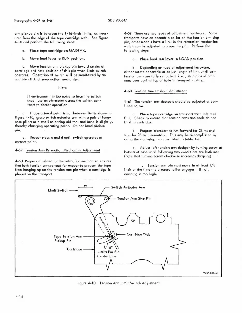
Paragraphs 4 .... 57 to 4-61 SDS 900647
arm pickup pin is between the 1/16-inch limits, as measured from the edge of the tape cartridge web. See figure 4-10 and perform the following steps:
a. Place tape cartridge on MAGPAK.
b. Move load lever to RUN position.
c. Move tension arm pickup pin toward center of cartridge and note position of this pin when I imit switch operates. Operation of switch will be manifested by an audible click of snap action mechanism.
Note
If environment is too noisy to hear the switch snap, use an ohmmeter across the switch contacts to detect operation.
d. If operational point is not between limits sho~n in figure 4-10, grasp switch actuator arm with a pair of longnose pliers or a small soldering aid tool and bend it slightly, thereby changing operating point. Do not bend pickup pin.
e. Repeat steps c and d unti I switch operates at correct point.
4-57 Tension Arm Retraction Mechanism Adjustment
4-58 Proper ad justment of the retraction mechanism ensures that both tension arms retract far enough to prevent the tape from hanging up on the tension arm pin when a cartridge is placed on the transport.
4-59 There are two types of adjustment hardware. Some transports have an eccentric collar on the tension arm stop pin; other models have a link in the retraction mechanism which can be adjusted to proper length. Perform the fo 1I0w i ng steps:
a. Place load-run lever in LOAD position.
b. Depending on type of ad justment hardware, either rotate eccentric or adjust length of link until both tension arms are fully retracted; i. e., stop pins of both arms bear against top of hole in transport casting.
4-60 Tension Arm Dashpot Adjustment
4-61 The tension arm dash pots shou Id be ad justed as outlined below.
a. Place tape cartridge on transport with left reel full. Check to ensure that tension arms and reels do not bind in cartridge.
b. Program transport to run forward for 26 ms and stop for 26 ms alternately. This may be accomplished by using the start-stop program I isted in table 4-8.
c. Adjust left tension arm dash pot by turning screw at bottom of tube unti I following two conditions are both met (note that turning screw clockwise increases damping):
1. Tension arm pin must move in at least 1/8 inch at the time the pressure roller engages. If not f damping is too high.
Switch Actuator Arm Limit Switch
Tension Arm Stop Pin
-" -..--- Cartri dge Web Tape Tension Arm ---i-----::::>""I!"-M41..1.
4-14
Pickup Pin
Cartridge --..... Limits For Pin Center Line
Figure 4-10. Tension Arm Limit Switch Adjustment
900647B.50

SDS 900647 Paragraphs 4-62 to 4-70
2. Arm should move out to "run" position and not bounce inward againi i. e., no osci Iloti ons. If the arm bounces or oscillates more than once, the damping is too low.
d. Repeat for right dash pot with tape alternately running reverse and stopping, and with ri~~ht reel full.
4-62 Tension Arm Pickup Pin Adjustment
4-63 The tension arm pickup pin should be perpendicular to the center line of the tape path (that is, perpendicular to the transport casting surface) when under tension. If it is not, the tape is driven against the inside of the cartridge housing as it winds onto the reel. This eventually causes the reel to bind in the cartridge housing. This binding can occur when a cartridge wound on a poorly adjusted transport is run on another transport, regardless of whether the second transport is properly adjusted or not.
4-64 This adjustment is made at the factory and should not have to be made again unless the pin is accidentally bent. To make the adjustment, perform the following steps:
a. Place properly wound tape cartridge on transport.
b. Place AUTO-MANUAL switch in MANUAL and press FORWARD button.
c. Observe how tape passes over right tension arm pin as it winds onto right reel. Tape should be centered in cartridge housing as it travels over cartridge pin. There should be approximately 0.030 inch clearance between tape edge and cartridge housing on each side.
d. If tape is not centered, tension-·arm pin should be adjusted by bending slightly. This is essentially a trialand-error method which involves removing the cartridge, bending the pin, replacing the cartridge, and seeing how the tape runs over the pin. The pin is bent by inserting a 5/16-inch-diameter aluminum rod with a 1/8-inch hole over the pin cmd bending.
e. The adjustment procedure is the same for the left tension arm pin except that the tape must be run in the reverse direction to see how it winds onto the left reel.
f. Check rewind operation to ensure that tape winds onto left reel properly. If the pin is adjusted properly in step e above, tape should rewind in the center of the cartridge.
4-65 Tape Cartridge Fit Ad justments
4-66 In general, proper tape cartridge fit requires two conditions: first, the cartridge must be seated firmly on the transport i second, the cartridge reel must be located correctly with relation to the cartridge h,::>using. Both of these factors affect tape guiding across the read/write head and tape winding on the reels. Incorrect' cartridge fit
results in tape buckling at the edges, binding, winding unevenly, etc. Refer to section II of this manual for instructions on cartridge loading procedure.
4-67 Cartridge Seating. The tape cartridge is held firmly in place by two spring clips which hold the sides of the cartridge, two locator pads on the transport casting, and a nylon hold-down button, the shaft of which slides into a notch at the bottom center of the tape cartridge. In addition' two positioning pins at the bottom of the transport casti ng serve as loading locations. If these pins are too low, the tape wi II bind between the top of the cartridge and the head guides. If they are too high, the cartridge cannot be loaded. When the cartridge is loaded on the transport, there should be a O. 005-inch to 0.020-inch clearance (depending on cartridge tolerances) between the bottom of the cartridge and the positioning pins. The positioning pins are C'djusted by bending them up or down.
4-68 If a tape cartridge adjustment fixture (SDS part No. 126603) is avai lable, the positioning pins can be adjusted as follows:
a. Place adjustment fixture on transport.
b. Tighten two nylon screws on top of adjustment fixture against head guide pins so that fixture is locked in place.
c. Insert a O. 007-inch thickness gauge between positioning pins and bottom of adjustment fixture.
d. Bend pins up or down until a slight resistance to the movement of the thickness gauge is felt.
e. Loosen plastic screws and remove adjustment fixtlJre.
4-69 Cartridge Reel Location. The cartridge reels should turn freely in the cartridge housing. In order to do so, the reel motor hubs should pick up the cartridge reels and center them in the plane of the cartridge housing so that there is approximately 0.030 inch between each inside surface of the cartridge housing and the edge of the tape. Also, the reel motor hubs should not touch the cartridge housing or scrape against it as they rotate.
4-70 The front surface of the reel motor hubs should be a distance of 0.207 inch ±O. 005 inch above the locator pads and hold-down button base (which are on the same plene). This adjustment is mede at the factory end should not have to be made again unless a part is replaced. A special adjustment fixture (SDS part No. 126603 is required to set the reel motor hub height correctly. See fi gure 4-11 and perform the fo Ilowi ng steps:
a. Place adjustment fixture on transport.
b. Tighten two nylon screws at top of fixture against head guide pins so that fixture is locked in place.
4-15
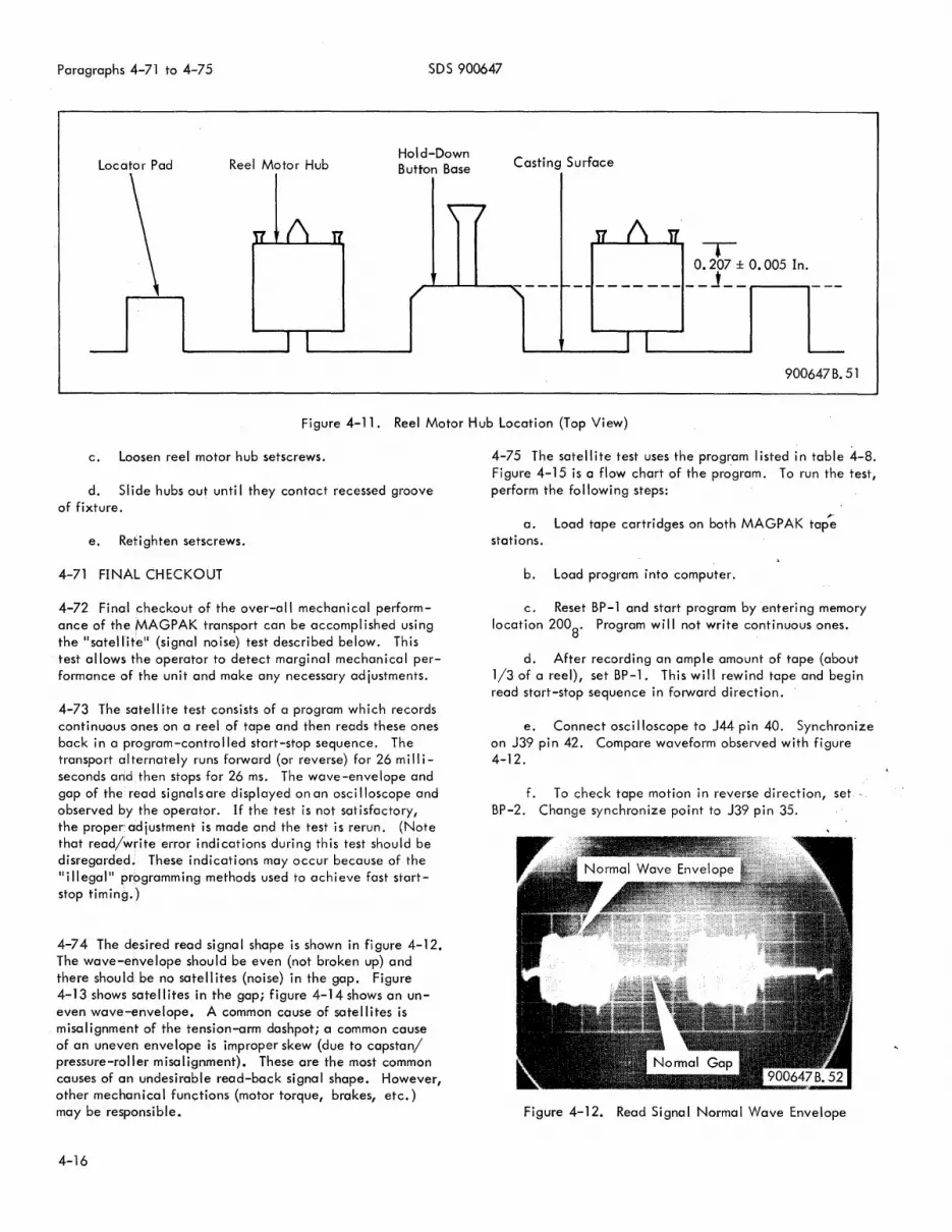
Paragraphs 4-71 to 4-75 SDS 900647
Locator Pad Reel Motor Hub Hold-Down Button Base Casting Surface
--.--0.207 ± 0.005 In. ___________ J __ ~---~
900647B.51
Figure 4-11. Reel Motor Hub Location {Top View}
c. Loosen reel motor hub setscrews.
d. Slide hubs out unti I they contact recessed groove of fixture.
e. Retighten setscrews.
4-71 FINAL CHECKOUT
4-72 Final checkout of the over-all mechanical performance of the MAGPAK transport can be accomplished using the "satellite" {signal noise} test described below. This test allows the operator to detect marginal mechanical performance of the unit and make any necessary adiustments.
4-73 The satell ite test consists of a program which records continuous ones on a reel of tape and then reads these ones back in a program-controlled start-stop sequence. The transport al ternately runs forward {or reverse} for 26 mill iseconds and then stops for 26 ms. The wave-envelope and gap of the read signals are displayed on an osci Iloscope and observed by the operator. If the test is not satisfactory, the proper: ad iustment is made and the test is rerun. (Note that read/write error indications during this test should be disregarded. These indications may occur because of the "illegal ll programming methods used to achieve fast startstop timing.)
4-74 The desired read signal shape is shown in figure 4-12. The wave-envelope shou Id be even {not broken up} and there should be no satell ites {noise} in the gap. Figure 4-13 shows satellites in the gap; figure 4-14 shows an uneven wave-envelope. A common cause of satellites is misalignment of the tension-arm dashpot; a common cause of an uneven envelope is improper skew {due to capstan/ pressure-roller misalignment}. These are the most common causes of an undesirable read-back signal shape. However, other mechanical functions {motor torque, brakes, etc.} may be responsible.
4-16
4-75 The satellite test uses the program listed in table 4-8. Figure 4-15 is a flow chart of the pr~gram. To run the test, perform the fo Ilowi ng steps:
a. Load tape cartridges on both MAGPAK tap~ stations.
b. Load program into computer.
c. Reset BP-1 and start program by enteri ng memory location 200
8, Program will not write continuous ones.
d. After recording an ample amount of tape {about 1/3 of a reel}, set BP-1. This will rewind tape and begin read start-stop sequence in forward direction.
e. Connect osci Iloscope to J44 pin 40. Synchronize on J39 pin 42. Compare waveform observed with figure 4-12.
f. To check tape motion in reverse direction, set BP-2. Change synchronize point to J39 pin 35.
Figure 4-12. Read Signal Normal Wave Envelope

SDS 900647
Figure 4-13. Read Signal Gap Noise Figure 4-14. Read Signal Uneven Wave Envelope
r-------------------------------~-------------------------------------------------------------------
SCAN REVERSE
L-________ . ________________ ~------------___________________________________ 9_0_0647B.~ J Figure 4-15. Satellite Test Program Flow Chart
4-17

SDS 900647
Table 4-8. Satellite Test Program Table 4-8. Satellite Test Program (Cont.)
Memory Instruction Instruction Memory Instruction Instruction Location Code (Octal) Mnemonic Rema;-ks Location Code (Octal) Mnemonic Remarks
INITIALIZE READ TEST
200 04020400 BPTl Breakpoint 1 set? 217 o 43 00235 BRM Mark place and branch to load-
201 00100217 BRU Yes; branch to read point subroutine
test 220 o 43 00227 BRM Mark place and
202 043 00227 BRM No; mark place and branch to ready branch to ready subroutine subroutine
221 o 40 20200 BPT2 Breakpoint 2 set? 203 043 00235 BRM Mark place and
branch to load- 222 o 01 00215 BRU Yes; branch to scan point subroutine reverse in b i na ry
204 043 00227 BRM Mark place and READ FORWARD branch to ready subroutine 223 0020361n RTB No; read tape in
binary; unit n WRITE DATA
224 043 00242 BRM Mark place and 205 0020365n WTB Write tape in branch to delay
binary; unit n subrouti ne
206 o 12 00212 MIW Memory into W- DI SABLE READ buffer when empty
225 002 00601 RKB Read keyboard 207 04020400 BPTl Breakpoint 1 set?
226 001 00247 BRU Branch to re-start 210 001 00217 BRU Yes; branch to delay
read test READY SUBROUTI NE
211 001 00206 BRU No; branch to MIW write constant 227 00000000 Branch return
212 77777777 Write constant (a II 230 o 40 21000 BRTW W-buffer ready? ones)
231 o 01 00230 BRU No; branch to 213 00000000 Write constant (a II ready test
zeroes) ? 232 040 1041n TRT Yes; tape ready
214 051 00242 BRR Return branch for test; unit n delay subroutine
233 o 51 00227 BRR Tape ready; return branch
SCAN REVERSE
234 o 01 00232 BRU Tape not ready;
215 o 02 0763n SRB Scan reverse in b ina ry; un it n
branch to tape ready test
LOAD POINT SUBROUTINE 216 001 00224 Branch to BRM-
delay subroutine 235 000 00000 BRM BRM return
4-18

SDS 900647
Table 4-8. Satellite Test Program (Cont.) Table 4-8. Satellite Test Program (Cont.)
Memory Instruction Instruction Memory Instruction Instruction Location Code (Octal) Mnemonic Remarks Location Code (Octal) Mnemonic Remarks
.-
236 002 1401 n REW Rewind; unit n 245 o 01 00244 BRU Branch to BRX
237 o 40 1201 n BTT Beginning of tape? 00035500 Delay constant fOI
240 051 00235 BRR Yes; return branch 246 or
910/920 Computers
o 0027000 Delay constant for 241 001 00237 BRU No; branch to BTT 925/930/9300
Computers DELAY SUBROUTINE '-
RESTART DELAY 242 00000000 BRM return .-
247 04300242 BRM Mark place and 243 071 00246 LDX Load Index Register branch to de lay
with delay consta"nt subroutine
244 o 41 00214 BRX Increment Index 250 o 01 00221 BRU Branch to BP-2 Renister and branch read test
4-19/4-20

SDS 900647 Paragraphs 5- 1 to 5-3
SECTION V
PARTS LIST
5-1 GENERAL
5-2 This section contains tables listing I·he replaceabl e parts for the MAGPAK Tape System. Only those parts recommended for replacement in the field are I isted. Each table is accompanied by one or more illustrations showing the locations of the parts.
5-3 In each table, parts are listed in alphabetical order,
and indentions are used in the DESCRIPTION column to
show parts relationsh ip. Parts manufacturers are I isted in
each tabl e by suppl ier code number. The name and address of the manufacturer can be found from the code number by using the suppl ier code index in table 5-21.
Table 5-1. Model 9446 Replaceable Parts
Fig. & Index No. Description
5-1- Assembly, Model 9446
55 Block, terminal molded barrier
35 Brake, magnetic, 28vdc
5-2 Cable assembly, plug module
Diode, SDS 103
Resistor, 3.9k, 2%, 1/2w
5-3 Coble assembly, plug module
Capacitor, tantalum, 100 fJf, 20%, 20v
Capacitor, mylar, 0.0047 fJf, 20%,20v
Diode, SDS 103
Diode, Zener, SDS 108
Inductor, molded, 10 ph, 5%
Resistor, 47 ohm, 2%, 1/2w
Capacitor, oil impregnated, 2 fJf, 20%
Capacitor, tantalum, 15 fJf, 20%, 50v
Capacitor, my I a r, O. 1 5 IJ f, 1 0%
Capacitor, oi I impregnated, 0.25 fJf, 20%
Connector, soldertail, 47 pin
Diode, SDS 113
Fuse, 3AG, 2 amp, 250v
Head, stack, magnetic tape, SDS 106722
Lamp, min iature incandescent
Reference Suppl ier Code Designator (See table 5-21)
SDS
TB3-L, TB3-R 51
Ll-L, L 1-R 160 L2-L, L2-R
P82 SDS
CR1-CRll 4,12,13,14
R5, R6 36,38,73
P83-P84 SDS
Cl, C2 26,27,74
C3,C4 26,27,74
CR1-CR7 4, 12, 13, 14
CR8, CR9 13,15,28
L 1, CR1-CR7 49,90,91
P84Rl, 36,38,73 P83R l-R15
C 1 L-C3L, 80,81 C1R-C3R
C4L-C6L 22,23,77 C4R-C6R
C7L, C7R 26,27,74 C8L, C8R
C9L, C9R 80,81
J26-J45 82
C R 1 L-CR3L, 26,30,68 CR 1 R-CR3R
Fl 48
166, 167
OS 1 L-OS5L, 163 OS 1 R-OS5R
Part No. --
107636
FB-090
107805
lN914A
107806
1N914A
lN964A
lN189
CF03
Qty
') '/ ..
4
22
4
7
16
16
6
6
4
2
20
6
2
10
5 ·1
Fig. & Index No.
5-1
5-1
5-1
5-1
5-1
5-1
5-1
5-1
5-1
5-1
5-1-5
5-1-6
5-1-68
5-1-60
5-2
SDS 900647
Table 5-1. Model 9446 Replaceable Parts (Cont.)
Description
Lamp, incandescent
Module, Cable Driver AX14 (See table 5-3 for replaceable parts)
Module, DC FI ip-Flop FH 19 (See table 5-6 for replaceable parts)
Module, Diode Gate GK51 (See table 5-10 for replaceable parts)
Module, Data Ampl ifier HX29 (See table 5-11 for replaceable parts)
Module, Read Amplifier HX30 (See table 5-12 for replaceabl e parts)
Module, Gate Write Ampl HX31 (See table 5-13 for replaceable parts)
Module, Photo Sense Ampl HX48 (See table 5-14 for replaceable parts)
Module, AND/OR Inverter IH 10 (See table 5-15 for replaceable parts)
Module, Inverter Ampl ifier IK51 (See table 5-18 for replaceable parts)
Module, Relay Driver RK53 (See table 5-19 for replaceable parts)
Motor, capstan drive, SDS 107650
Motor, reel, SDS 107225
Post, extractor, fuse
Relay, 24 vdc
Resistor, variable, 2k, 10%
Resistor, variable, 500 ohm, 10%
Res istor, 22 ohm, 2%, l/2w
• Resistor, 12k, 2%, l/2w
• Resistor, 47 ohm, 2%, l/2w
Resistor, 100 ohm, 2%, 25w
Resistor, 56 ohm, 2%, l/2w
Resistor, 82 ohm, 2%, l/2w
• Res istor, 1. 2k, 2%, l/2w
Socket, relay mounting
Reference Designator
DS6L, DS6R
M1L, M1R
M2L, M2R
XFl
Kl L, Kl R, K2L, K2R
R 1 L, Rl R, R2L, R2R
R3L, R4L, R3R, R4R
R7L, R7R
R8L, R8R
R9L, R9R RlOL, RlOR
Rll L, R12L, Rll R, R12R
R131, R13R
R14L, R14R
R15L, R15R
XK1L,XK1R, XK2L, XK2R
Suppl ier Code (See table 5-21)
84
SDS
SDS
SDS
SDS
SDS
SDS
SDS
SDS
SDS
SDS
165
165
48,49
164
45, 100
45, 100
36, 38, 73
36, 38, 73
36, 38, 73
36, 38, 73
36, 38, 73
36, 38, 73
36, 38, 73
164
Part No.
253
102853
103134
100246
103387
103370
107429
117696
100137
100388
100905
HPK-N-342002
KHP-17Dll
27E006
Qty
2
2
4
2
2
2
2
1
4
4
4
2
2
4
4
2
2
2
4

SDS 900647
Table 5-1. Model 9446 Replaceable Parts (Cont.)
Fig. & Reference Supplier Code Index No. Description Designator (See tab Ie 5-21)
5-1-60 . Solenoid, 25 vdc L3L, L3 R, 161 L4L, L4R
. Switch, rotary, 12 position S 1 L, S 1 R, 55 S2L, S2R
Switch, toggle, dpdt S3L, S3R 106
Switch, pushbutton S4L-S7L 113 S4R-S7R S 13L, S 13R
Switch, spring action S8L, S8 R, 162 S9L, S9R
Switch, snap action S lOL, S lOR 162 S 11 L, S 11 R
Transistor, si I icon photo conductive Q1 L, Q1 R, SDS Q2L, Q2R
Part No. -
A-348-2
PA-2001
83054-SE
Cl13-P-3
lSM1
V3
108272
Qty t-
4
4
2
10
4
4
4
53

~HASSIS
00
5-4
SDS 900647
MODULE LOCATION CHART
LOCATION 4S 44 4, 42 41 40 39 38 37 3' 35 34 33 32 3; 30 29 28 27 26
TYPE HX HX IH IK GK HX RI< AX II< GK HX FH GK GI< RI< AX 30 Z9 10 51 51 31 53 1<4 51 51 ~e 19 51 51 53 I" 3 3 2 6 6 2 2 3 8 20 2 2 5 16 2 2 8 20 6 £» KEY
39 31 44 34 34 8 22 41 22 24 8 ZZ II 40 ZZ ZZ 22 H 36 38
1-\-'\--0
00000 0..(0 0 0 0
~ ~ O~ ~OOOO~
o
o
@ O~O~ @
13
II
<:> <:>
Front and Side Views
J.\-~
ASSV. MA6PAI<.
ASSV NO. 107636
MODEL NO 944&
Figure 5-1. Model 9446 Assembly (Sheet 1 of 3)
/
r® /
l07636-1F
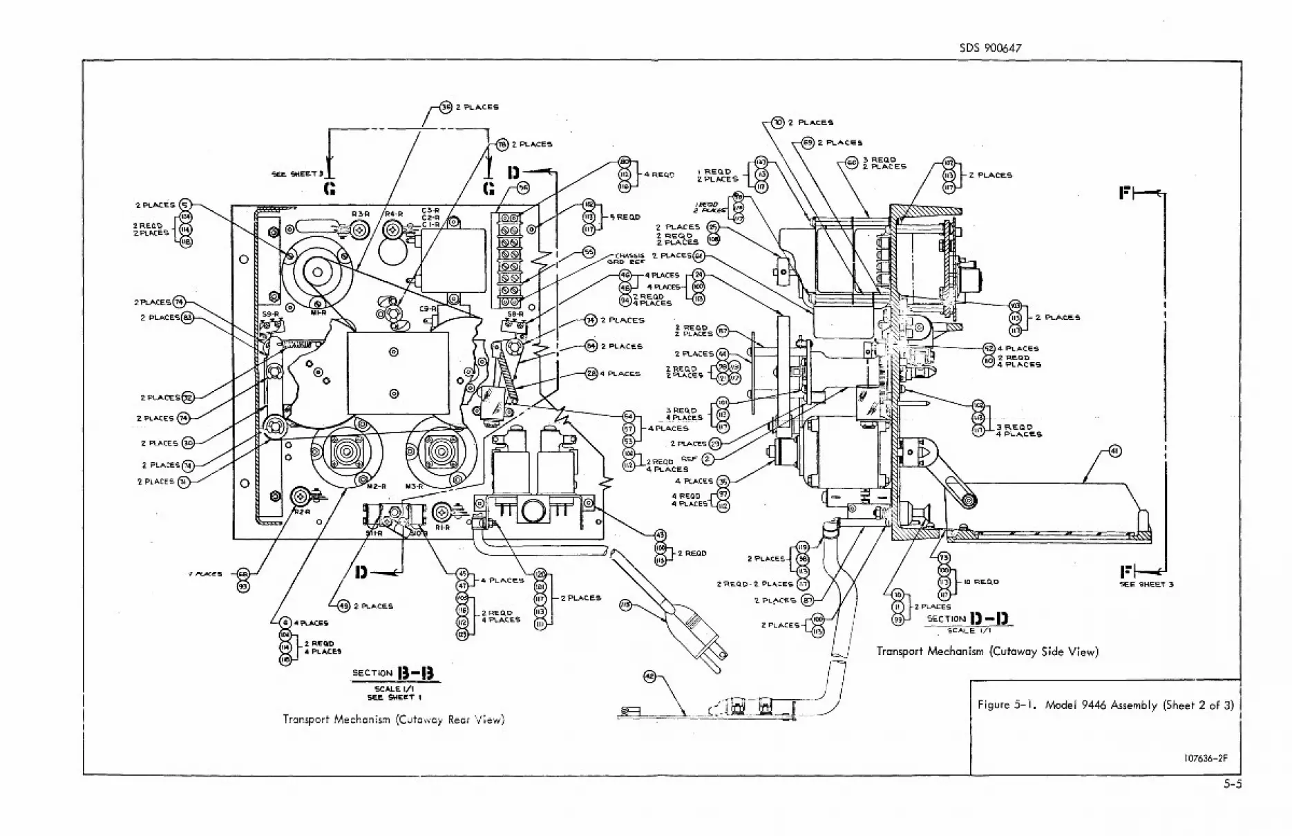
2 REo..t> ZPLACES
:2 PLACES '74
2PlACES~
SECTION II-II SCALE III
see. S\1EET I
Transport Mechanism (Cutaway Rear View)
2 REQ.D 2 P\..ACES
3 REQ.O _ 4PLII.CES
2 PLAC.E.S ll"l
ZPLACES
SDS 900647
Z PLACES
SECTION I) -I) SCALE 1/1
Transport Mechanism (Cutaway Side View)
I:-"-~ SEE SHEET 3
Figure 5-1. Model 9446 Assembly (Sheet 2 of 3)
l07636-2F
5-5

2 REQO
o
~4PLAC-E~ 2 REQt>
109 4PL~c:.ES
VIE w 1::- - 1= 'SCALE '"
SEE SHEET Z.
~"P~CES
o o o
Cartridge Mounting Hardware (Cutaway Front View)
~'l
'2. PLACES 'n
4 PLACES
4 PLA.CE.S
5-6
VIEW C:- C: SCALE 1/1
SEE SHEET -.
Transport Mechanism Detail (Cutaway Top View)
SDS 900647
C\-R REF
C)-R REF
~f.cr,ot..l I~ -I~ ~c.A.'-£. 2./ I
Pressure Roller Assembly (Side View)
4 PLA.C.e.S
REF
Figure 5-1. Model 9446 Assembly (Sheet 3 of 3)
l07636-3F
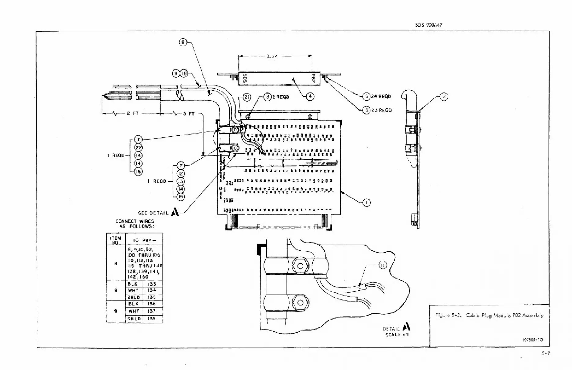
)
, I j
C2 FT -~.~1 .. -'V--3 FT
I
I REQD
I REQD
CONNECT WIRES AS FOllOWS:
ITEM NO
8
9
~
TO P82-
8.) 9.,,10) 92) 100 THRU 106 110.1" 2,113 115 THRUI32 138 I I 39 J I 4 I" 142,,160
BlK 133 WHT 134
SHLD 135
BLK 13&
WHT 137
ISHLOl135 I I
=1 "1_'t.B:::;;:~C::=S'lr,,~a
I z ... : I t:l I I ~ i! = i! :i ~ 3 : II ~ ~ j ~ =1 'as ~ o~.
8 t ~:::.: ~ : :: !! ;: :: ;: ;:: :::i : ~ a :: !! :I ~ : " !! ~ I ~ ~ e • ~ • = ~ ~ ~ ~ : ~ · ~ · ~ = • ~ ~ ~ -: ...... !'!!
t~11II
SDS 900647
5 23 REQO f
" \ \ I U
DETAIL ;\ SCALE 2:1
Fig!Jre 5-2. Cable PIi.Jg Module P82 Assembly
l07805-1G
5-7

Ul o (})
s--
c:: ::..=::J
20 FT BETWEEN
CABLE CLAMPS
4 REQD
5-8
(J)
o (J)
SDS 900647
5-0 ---5
7 48 REQD
6 46 REQD
Figure 5-3. Cable Plug Module P83-P84 Assembly
107806-1 H
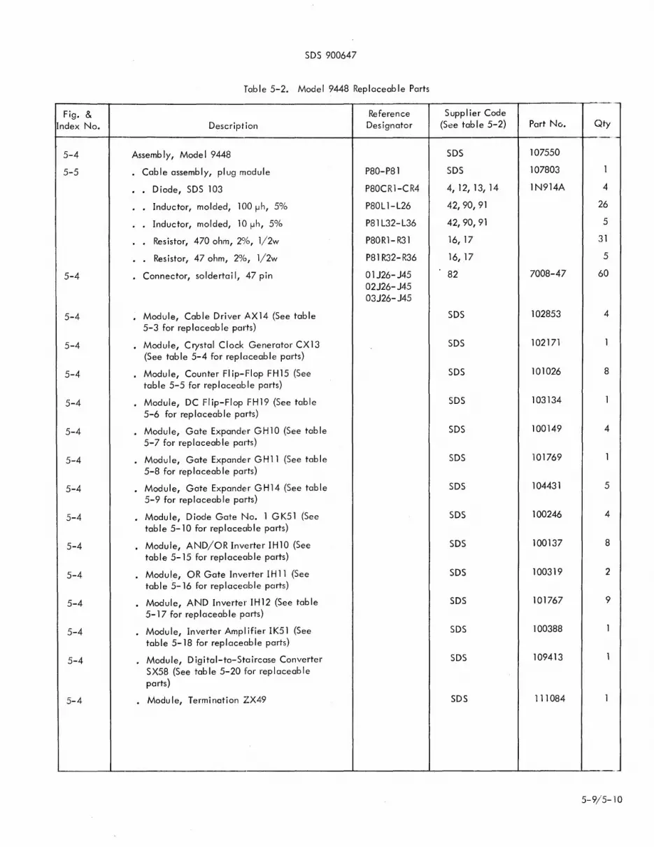
SDS 900647
Tab Ie 5-2. Model 9448 Replaceab Ie Parts
Fig. & Reference Suppl ier Code Index No. Description Designator (See tab Ie 5-2) Part No. Qty
5-4 Assembly, Model 9448 SDS 107550
5-5 Cable assembly, plug module P80-P81 SDS 107803 1
Diode, SDS 103 P80CR1-CR4 4, 12, 13, 14 lN914A 4
Inductor, molded, 100 fJh, 5% P80l1-l26 42,90,91 26
Inductor, molded, 10 tJh, 5% P81 l32-l36 42,90,91 5
Resistor, 470 ohm, 2%, l/2w P80Rl- R31 16, 17 31
Resistor, 47 ohm, 2%, 1/2w P81 R32-R36 16, 17 5
5-4 Connector, soldertail, 47 pin 01J26-J45 82 7008-47 60 02J26-J45 03J26-J45
5-4 Module, Cable Driver AX14 (See table SDS 102853 4
5-3 for rep laceab Ie parts)
5-4 Module, Crystal Clock Generator CX13 SDS 102171 1
(See table 5-4 for replc)ceable parts)
5-4 Module, Counter Flip-Flop FH15 (See SDS 101026 8
table 5-5 for replaceab Ie parts)
5-4 Module, DC Flip-Flop FH19 (See table SDS 103134 1
5-6 for replaceable parts)
5-4 Module, Gate Expander GH10 (See table SDS 100149 4
5-7 for replaceable parts)
5-4 Module, Gate Expander GH11 (See table SDS 101769 1
5-8 for replaceable parts)
5-4 Module, Gate Expander GH14 (See table SDS 104431 5
5-9 for replaceable parts)
5-4 Module, Diode Gate No. 1 GK51 (See SDS 100246 4
table 5-10 for replaceoble parts)
5-4 Module, AND/OR Inverter IHlO (See SDS 100137 8
table 5-15 for replaceable parts)
5-4 Module, OR Gate Inverter IH11 (See SDS 100319 2
table 5-16 for replaceable parts)
5-4 Module, AND Inverter IH12 (See table SDS 101767 9
5-17 for replaceable parts)
5-4 Module, Inverter Amplifier IK51 (See SDS 100388 1
table 5-18 for replaceable parts)
5-4 Module, Digital-to-Staircase Converter SDS 109413 1
SX58 (See table 5-20 for replaceable parts)
5-4 Module, Termination ZX49 SDS 111084 1
5-9/5-10

0
0
j\
j\
0
I sJDL~ I co~i*6t~E~ I L ASSV No.I07550
~1 ____ ~!_~_O_E_l_OO __ .9_4_4_e ___ I~l ~
DETAIL I~ sCAL£ 1:/
5££ DETAIL II
0
0
SIDE VIEW
/~
, ,
----
0
CHASSIS
0 01
---- -----
II
CHASSIS
02
'I 11 I-I
CHlSSTS ! f I 03
---.I.
ii
0
0
0
FRONT VIEW
LocATION 45 44 43
TYPE SX 58
KEY 4 24
LOCATION 45 44 43
TYPE IH IH IH IZ 12 12
KEY to fO 10 34 34 34
LOCATION 45 44 43
. TYPE P P 81 83 6 6 KEY 32 32
SDS 900647
MODULE LOCATION CHART
42 41 40 39 38 37 36 35 34 33 32 31 30 29 28 27 26 IH IH IH FH FH IH IH IH GK GH GH GH FH FH FH 12 12 .... 15 15 iO . " IC 51 JO 14 14 15 i 5 15 IV IV
10 10 2 8 8 2 2 2 2 2 30 30 8 8 8 34 34 44 30 30 44 44 44 ZZ 40 34 34 30 30 30
42 41 40 3'3 38 37 36 35 34 33 32 31 30 29 28- -27 26 IH IH F~ FH GH IH IH GK GK ~~' r: r~ GH GH (lH -~lf Flf II II 15 15 " 10 10 51 51 .10 10 10 15
2 2 8 8 to Z Z 2~ 2 30 30 i~ ~ 4~ '"2- T~ ~
16 16 30 30 26 44 44 22 34 34 40 40 30
42 41 40 39 38 37 3G 35 34 33 32 31 30 Z9 28 21 26 P ZX AX AX AX AX IK IH IH IH IH IH IH GK lex
83 49 14 14 14 14 51 lZ 12 12 12 10 10 51 13 6 6 20 20 20 20 i 10 ~~ ~~ i~~ 14 4
24 2i 1~ 36 28 24 24 24 24 34
Figure 5-4. lvkdel 9448 Assembly
107550-18
5-11

o
REF
TYP r 3•54
I C/'I a C/'I
--5--0--5
.. N N 1iI!:l N 1:1 r::l N N!II '!!! '!!!!l!:II N"!l! I iii f lI O . leg ilINC5ii.Ji"'o."'~215 • N
."_~'1
4.1 FT BETWEEN
CABLE CLAMP5
2 REQD
4 REQD
SEE DE TAIL ~\
DETAIL ~\ TYP BOTH ENDS OF
BOTH CABLES
SCALE:X
5-12
(/'I o (/'I
SDS 900647
--5 -·-0 --5 'U
0)
I ..... ..-----4FT TVP -----....,
I y
Figure 5-5. Cable Plug Module P80-P81 Assembly
107~03-1E

Fig. & Index No.
5-6
SDS 900647
_R5-7 _ I'- _CR8-7 -0 ~ _ R6-7_
-R4-7--::-- 50 2.00 O~ _RIO-7_ o-CRI-7 - (\J R9-7 o-CR3-7 _ Y --
_ R3-7_
_ R5-6_
_ R4-6 _ -
o-CRI-6_
o-CR3-6.. _ R3-6_
_ R5-5_
_R4-5 _ -
o-CRI-5-o-CR3-5_
_ R3-5_
R6-6 (0 CR8-G..o Q - (0
130- O~O~ _RIO-6_ 5 _R9-6_
(01
It) "" It) _CR8- 5-o .;. 0 ,:., - R6-5
~0~00 00 _RIO_-5_
o 5 - R9 5_
I R6-4
R7-7 _
_ VR2-7 -t> -CR6-7-o
o-CR5-7_ -CR7-7-o
_ R7-6 _
- VR2-~{> -0 CR5-6 CR6-6
0-: -CR7-6-o
- _ R7-5 _
_VR2-5-t> o-CR5_5_CR6-5-o
-CR7-5-o
R7-4 _ ! _CR8-4-o Q - "t -00 0 (\J'f O~ -RIO-4_ - VR2-
4-t> - R5-4_ -CR6-4-o _ R4-4_ 5 - R9-4_ o-CR5-4_
"T I -CR7-4-Q o.CRI-4 - ,..., ,..., g ,..., _ R6-3 _ R7-3 _
-o,;~~:"- ~u~Oi; ~u? 00,," O~ -RIO-3 - - VR2-3-[>
- R5-3- ... _ R9-3 _ o-CR5_3-_CR6-3-Q
_ R4-3_ I I -CR7-3-o
o-CRI 3 R6-2 _ R7-2 -- - ~ _CR8-2-o Q - C)J -
_ q;~:3~ __ 0 O~O ~ 0 8 =:I~_: = ;.~::~:~t6-2-{) _ R5-2 _ 0 I - CR7-2-0
- R4-2 _ _CR8-1 -0 ~ ;J; - R6-1 - R7-1 -
o-CRI-2 - _ Q 0 0 RIO-I _ VR2-1 -f> o-CR3-2_ .1.. O~ 00 - - -CR6-I-o
R3-2 0 a:: - R9-1 - I""\....CR5-1_ - - u \J. CR7-1 -0
- ~- _CRI-II-o ~O -CR4 -0 1 1- I I _ R4-1 _ o-CR3-1- _ VRI -t> <D I
- CI -0 a:: s:! it: ~ 0- C2 1 1 1
Figure 5-6. Coble Driver AX14 Ports Location
Table 5-3. Coble Driver AX14 Reploceble Ports
Reference Suppl ier Code Description Designator (See table 5-21)
Cable Driver AX14 (See tables 5-1 and SDS 5-2 for next assembly)
. Capacitor, tantalum, 4.7 fJf, 20%,50v Cl, C2 22,23,77
Diode CR1, CR3 4, 12, 13, 14 thru CR8
Diode CR2 13,15,28
Diode VR1, VR2 2, 12, 13, 14
Resistor, 3. 9k, 2%, l/2w R 1, R2, R4, R5 16, 17
Res istor, 8. 2k, 2%, l/2w R3 16,17
Resistor, 22k, 2%, l/2w R8, Rl0 16,17
Resistor, 39k, 2%, l/2w R9 16,17
Transistor, SDS 209 Q1, Q2, Q4 7 1 3
Transistor, SDS 220 Q3 3, 11 1
PIN 1
CONNECTOR END
PIN 47
Part No.
102853
lN914A
lN921
lN746
2N2477 2N2538 2N2848
2N2369 2N2501
102850
Qty
2
43
7
8
16
7
8
7
15
7
5-13

Fig. & Index 1'10.
5-7
5-14
SDS 900647
Table 5-4. Crystal Clock Generator CX13 Replaceable Parts
Description Designator
Crystal Clock Generator CX13 (See table table 5-2 for next assembly)
Capacitor,
Capacitor,
Capacitor,
Capacitor,
Capacitor,
Capacitor,
Capacitor,
Capacitor,
Capacitor,
r-
L-
tantalum, 15 fJf, 20%, 20v C1, C5
mica, 100 pf, 5% C2
mica, 47 pf, 5% C3, C4
mica, 150 pf, 5% C6, C7
mica, 470 pf, 5% C8
mylar, 1500 pf, 10% C9
mylar, 4700 pf, 10% ClO
mica, 510 pf, 5% C11
tantalum, 4.7 fJf, 20%,50v C12
_CRB -0 _CR9 -0
I I _CR7 -0 N N _CRIO -0 N a:: a:: _CRII -0
_CR6 -0
q Jifl N N -a:: a:: r<l U
I~ I I
(0 0 0
r<l
--- n: ~ _ R20 _ I N
_ RI9 a:: - >
_RIB _ 19
00 r<l a:: u
I
_ R3 -_ R4 -
0- CI2
I I I en
(0 r-N N a:: a:: a::
I I I
~I
I r<l
b
r<l r- U a::
00 a::
r
0
0
0 D
>=
_ C2 _
_ CIO _
_ C6
en r- oo U U U
_ C4
_ RI2 -_RII -_ RIO _
I _ C5 -0
ct:>NOO:£ 9 I _R14 _ ..l. I Nil') V a:: a:: - R2 -
~ ~O I ~6 _R17
qO~ -q'o- CI o Ia::a:: ___ _
I " ~ '1'6 - R16;- I _ LI _ _ RI _ ~
_ CI3 - 0- CI4
Suppl ier Code (See tab Ie 5-21)
SDS
22,23,76
19,20,21
19,20,21
19,20,21
19,20,21
26,27,74
26,27,74
19,20,21
23,77
Il') N a::
Figure 5-7. Crystal Clock Generator CX13 Parts Location
Part No. Qty
102171
2
1
2
2
1
1
1
1
1
PIN 1
CONNECTOR END
PIN 47
102168B

SDS 900647
Table 5-4. Crystal Clock Generator CX13 Replaceable Parts (Cont.)
,-----Fig. & Reference Suppl ier Code
Index No. Description Designator (See table 5-21) Part No. Qty
5-7 Crystal* Y1 138 1 (Cont. )
Diode CR1-CRll 4, 12, 13, 14 1N914A 11
Diode VR1 2, 12, 13, 14 lN752 1
Diode VR2, VR3 2, 12, 13, 14 lN746 2
Potentiometer, 1k, 10% R15 35,44 1
Resistor, 1k, 2%, 1/2w R1, R2, R5, 16, 17 5 R6, R9
Resistor, 3.9k, 2%, 1/2w R3, R16, 16, 17 4 R21,R22
Resistor, 820 ohms, 2%, 1/2w R4, R23 16, 17 2
. Resistor, 2.2k, 2%, 1/2w R7 16, 17 1
Resistor, 100 ohms, ~Ic), 1/2w R8 16, 17 1
Resistor, 1. 5k, 2%, 1/2w RlO 16, 17 1
Res istor, 4.7k, 2%, 1/2w R11, R14 16, 17 2
Resistor, 15k, 2%, 1/2w R12 16, 17 1
Res istor, 10k, 2%, 1/2w R13 16, 17 1
Resistor, 18k, 2%, 1/2w R17 16, 17 1
Resistor, 3. 3k, 2%, 1/2w R 18, R 19, R20 16, 17 3
Resistor, 39k, 2%, 1/2w R24 16, 17 1
Resistor, 47 ohms, 2%, 1/2w R25 16, 17 1
. Transistor, SDS 220 Q1-Q5, 3, 11 2N2369 5 1 2N2501 95 2N2710
Transistor, SDS 209 Q6 1 2N2538 1 7 2N2476 3 2N2848
... -*Crystal shall be housed in Military Holder type HC-6/U, HC-13/U or
HC-13/U with a 2.0-inch cover, and shall be adjusted to have the required frequency in series resonance at 600 C. The crystal cut and mode shall be determined as follows:
Frequency Range (Kc) Cut Mode
30 - 100 N Flexure
100 _. 250 E Extension
250 .• 500 C Face shear
500 .• 2000 A Th ickness shear
5-15

Fig. & Index No.
5-8
5-16
-
SDS 900647
_RII-4 - CI-4 _ _ _CRII-4 -0 CR16-4 " <f - R9 4 - _CRI2-4-o
0- -, v (\J00 ~ I f'lO 0 -CR5-4-o - R8-4 - v "f NOv v v :r "f 0 " _ R15-4 -
_RI3-4 _ ~ 0: a:: ~ ci: Nf'lm '!l ~"f l ~ ~ __ I I I I I or <..> ,>,5 Y a:: 5 I a: iE a::
-RI2-4 - or or v' °0 'tor6 ~ ~ 'r .; ~Vi6+~ - R7-4 - ;f ~ th a:: ~ <..> ~ Q ~ ~ ~ ~ _CR4- 4 -o
_RI4-4 _ _ C2-4 _ 0 6 _CR21-4-o - RIO-4 - _CR22-4f'\
o-CRII-3 '-'
o-CRI7-4_ I a::, 6 ~' I ~ <..> 66 _CR8-4 -01 RII-3 - CI-3 - - R9-3 - _CRI2-3 -o
- - I , , rp /\ 0 f'l 1 -CR5-3 -0 r<'l o-CRI6-3_ r<'l r<'l '? ~Oo'-r" Orp 0 Y rp , _RI5-3_1 <..>
R8-3 ..!.. rh (\J r<'l r<'l r<'l r<'l 10 r<'l rp r<'l r<'l - - a:: a:: a:: r<'l to ~ ~Om iE I ~ ~ (5 ~
_RI3-3_ 'I 'III..!.. 5'>'<..> 51'r<'l '<">'~'O'<">Q -- 00 'r<'lIr<'lAr<'l, ,r<'l Tro rp roA _ RI2-3_ ~:g rp ri- ~uci: ~ Q !i2 ~ 2!Vrp _CR4-3 -0
_ R7-3 _ a:: a:: £ 5 ~ y I 5 5 <..> 5 ~ _CR8-3 -0 <;> <; CRI7-3_ I I I 6 V' 6666 P _CR21-3 -0 ~~a::
ry -C2-3 - - RIO-3 - _CR22-3-o a:: - R14-3 - _ CR12-2-o ~ ~
o-CRII-2 - CI-2 - - R9-2 -, -CR5-2 -0 - RII-2 - I , I C)J 0 ~ 00 0 0 C)J , _ R15-2 _ 1
o-CR16-2 - (\J (\J C)J ~O 1 C)J ~ C)J !2 ~ I ~ , , (\J (\J (\J C)J (\J 10 a: ~ a:: r<'l a:: _R8-2 - iE ~ a:: to ii: (\JOm iE 1<,,>'5'6,5n <..>
R13-2 II I,IIC)J 51>~N5'1' C)J1t}J1~ t}Jo'T' 6 - - 00 '~'_'-V..i.. 1 (\J Q s! ~ 0> C)J _CR4-2 -o
-- ~ C)J (\J £r (\J ~ !2 5 5 <..> iE 2 _CR8-2 -0 ~ - R12-2 - v ~ ~ y ~ 1 a:: 6 6 6 C 5 _CR21-2-o
- R7-2 - 'I " 0'\7 I - RIO-2 - I _CR22'2-o o-CRI7-2_ - C2-2 - -CRI2-~-O
_RI4-2_ _R9-1 _ CR5-1 -0
r<'l a:: > I
o-CRII-I - -_ CI-I - 0 0 0 ~ ~ - R15-1 - <;> - RII-I _ , , I ~ 0 t;. 1 0- ;i; , !2 ~ 10
o-CRI6-1 __ , , 0'7' -, - oh ~ ~ ~'<">O CR4-1 ~S:! I ,." (\J tD .!. (\J 151 I lul,(r.iA. - -0 NU
- R8-1 - 0: a:: a:: 5 la::, a:: 0 0> 1 ,1''7'17 'V;; _CR8-I-o a:: I I - ><..>a:: oeoVO>(\J 1<">
- R13- - I I , I '5C1'7 '76'7'~ th a: iE ~ 5 a:: _CR2H -0 6 -- r- C\I 0: 0: <..> <..> <..> 0 <..> CR22-1 -0 I
_RI2-1_ va::'7' lOa::' 5 ~ T' I 666 1-
_ R7-1 _ 6'\7 - RIO-I - I I I ~ o-CRI7-1 _ I I - C2-1 C4, -leo
RI9 _ _RI4-1 £ S:! Ii: _ R20_ I I I
Figure 5-8. Counter Flip-Flop FH15 Parts Location
Table 5-5. Counter Flip-Flop FH15 Replaceable Parts
Reference Suppl ier Code Description Designator (See table 5-21)
Counter Flip-Flop FH15 (See table 5-2 SDS for next assembly)
Capacitor, mica, 330 pf, 5% Cl, C2 19,20,21
Capacitor, mylar, 0.01 fJf, 10% C3, C4 26,27,74
Diode CR1-CR29 4, 12, 13, 14
Diode VR1, VR2 2, 12, 13, 14
Diode VR3 2, 12, 13, 14
Resistor, 3.9k, 2%, l/2w Rl,R6,R17 16, 17
Resistor, 10k, 2%, l/2w R2, R5 16, 17
Res istor, 5. 6k, 2%, l/2w R3, R4 16, 17
PIN 1
CONNECTOR EN D
PIN 47
lOlOOlE
Part No. Qty
101026
8
2
lN914A 101
lN746 8
1N752 1
9
8
8

SDS 900647
Table 5-5. Counter Flip-Flop FH15 Replaceable Parts (Cont.)
Fig. & Reference Supplier Code Index No. Description Designator (See table 5-21) Part No. Qty
5-8 Resistor, 470 ohms, 2%, l/2w R7, R8, R21 16, 17 9 (Cont. )
Resistor, 120 ohms, 2%, l/2w R9, RI0, 16,17 16 R15, R16
. Resistor, 470k, 2%, l/2w Rll, R14 16,17 8
Resistor, lOOk, 2%, l/2w R12, R13 16,17 8
Resistor, 4.7k, 2%, l/2w R18 16, 17 1
Resistor, 47k, 2%, l/2w R19, R20 16, 17 2
Transistor, SDS 200 Ql, Q2 1,5,7,95 2N834 8
---
Table 5-6. DC FI ip-Flop FH 19 Replaceable Parts
Fig. & Reference Suppl ier Code Index No. Description Designator (See tab Ie 5-21) Part No. Qty
5-9 DC Flip-Flop FH19 (See tables 5-1 SDS 103134 and 5-2 for next assembly)
Capacitor, mylar, 0.01 fJf, 10% Cl 26,27,74 1
Diode CRI-CRll 4, 12, 13, 14 IN914A 66
Diode VR1, VR2 2, 12, 13, 14 1N746 12
Resistor, 3.9k, 2%, l/2w R 1, R2, 16, 17 24 R5, R6
Resistor, 820 ohms, 2%, l/2w R3, R4 16, 17 12
Resistor, 18k, 2%, l/2w R7, R8 16, 17 12
Res istor, 47k, 2%, l/2w R9 16, 17 1
Transistor, SDS 200 Ql, Q2 1,5,7,95 2N834 12
/
--
5-17

U1 I
00
" cO· e ro U1 I
;.0
o ()
" ""0
I
" o ""0
" I
-0
'iJ a ...., ..... '" ro ()
a -+
o :::l
0 tv
W 0 »
I I . 1 I I I 1 1 I 1 I I
j:u :u1«I::o ::olol:u ::o1«1:u :u1«1:u ~1<j>1:u ~I :u cI cp :Uo::O ~ cp :ul,::o cI CP:u o:u cI cP :Uo:U cI 1 :Uo~ cI ';;:u
() Y'- --f>::OCfN Nt:uY'<>I <>I"i'i2lY'''' "'''i'~Y'(JI UI"i'~' 01 '" 1, -I I -:eNI 1 NCD<>II 1 (.01 j,."'1 I ",~Ull I UI~OlI I en
~
~ 1 1 I I I P' 1 1 I 1 I I 1 I I I I ~
'00 0 0 0 0 0 (5 0 0 0 0 <l-VR2-L ~ <l-VR2-L ~ <l-VR2-3- $? <l-VR2-4- ~ <J-VR2-5- ~ <l-VR2-6..... ~
9<l-VR,-, _ ~0<J-VRI-L ~9,/LVRI-3_ ~ 9<}-VRI-4_ ~«<J-VRI-5- ~C;><l-VRI-6_ ~ (") - A NO....... <>I (") '" () UI (") 01 :u I ::0 I ::0 :u I ::0 I :u I I: o-CR:>-I- ~ o-CR:>-L ;:;; o-CR:>-3- I J: o-CR:>-4- &; O-CR3-5- ;;; O-CR:>-6-
I _CR4-I -o I -CR4-2-o I -CR4-3-o I -LR4-4-o I _CR4-5-o I _CR4"i5-o
_ R2-1 _
_R5-1 _
_ R6-1
_ RI-I _
_CR5- I -o
O-CR6- I -
-CR8- I -o
o-CRIO-I-
_R2-2 _
_R5-2_ ----_ R6-2 _
_ RI-2 _
_CR5-2.-o
O-CR6-2-
_CR8-2-o
O-CRtO-2--CR7-I-o _CR7-2-o
o-CRtI-1 - o-CRtI-2-
'iJ
Z ~ ""-l
_R2-3 _
_R5-3 _
_R6-3 _
_RI-3 _
.......cR5-3-o
o-CR6-3-
_CRS-3-o
O-CRlO-3.....
_CR7-3-o o-CR11-3-
()
0 Z Z m () -I
0 ;:0
m Z 0
_R2-4 _
_R5-4_
_R6-4 _
_RI-4 _
_CR5-4-Q
o-CR6-<L
_CR8-4-o
o-CRIOA
_CR7-4-o o-CRII-4_
_R2-5_
_R5-5 _
_R6-5_
_RI-5 _
-CR5-5-o
o-CR6-5-
_CR8-5-0
O-CRlO-5--CR7-5-o
O-CR1 1-5-
_R2-6 _
_R5-6_
_R6-6 _
_RI-6 _
_CR5-s-Q
o-CR6-G
_CR8-6-o
o-CRJO.ti
_CR7-6 -o o-CRt1-6_
~ z
l/'l o l/'l
-0 o o 0-~ ""-l
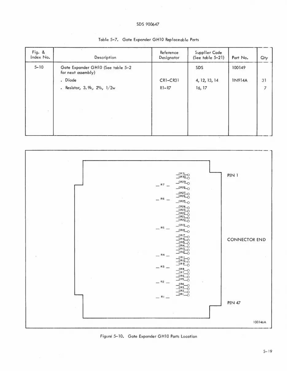
SDS 900647
Table 5-7. Gate Expander GH10 Replaceable Parts
Fig. & Reference Suppl ier Code Index No. Description Designator (See table 5-21) Part No. Qty
5-10 Gate Expander GH10 (See table 5-2 SDS 100149 for next assembly)
Diode CR1-CR31 4, 12, 13, 14 1N914A 31
Resistor, 3.9k, 2%, l/2w R1-R7 16, 17 7
_CR3-!:-o _CR3~ PIN 1
R7 _CR2~
_ CR21Lo CR2~
R6 _CR2~
_CR2~
_CR2~ _ CR2l...o _CR2Lo _CR2Lo _CR2Q....Q
R5 _CRILo
_CRIIL.o
_CRI~
CONNECTOR END _CRI§.....o
_~=I~ =CR~
R4 _CRIL..o
~RI!-o ~RI~
_R3 _ _CRL..o
_ CR8-o _ CR7-o
JR~
_R2 _ _ CR5-o
_ CR4-o _ CR3-o
_ CR2-o
_ RI_ JR1-o
PIN 47
lOOl46A
Figure 5-10. Gate Expander GH10 Parts Location
5-19

SDS 900647
Table 5-8. Gate Expander GH11 Replaceable Parts
Fig. & Reference Supplier Code Index No. Description Designator (See table 5-21) Part No. Qty
5-11 Gate Expande r G H 11 (See table 5-2 SDS 101769 for next assemb Iy)
Diode CR1-CR12 4, 12, 13, 14 1N914A 93
Resistor, 3.9k, 2%, l/2w R1-R4 16, 17 31
~RIO-EL R3-8
.-e:R9-~ R2-8 ~R3-F.L:Q
~R8-!L CR7-.ao RI-8 j;R2-8-<>
CR5-.§o ~R6-8_ R4-7_ J;RI- 8--a
~RI2-7_ R3-7_
~R4-7 __ CRII-Lo
~RIO-L - ~R3_7~R9-Lo R2-7
~R8-7_ RI-7
StR2_7-<5CR7
-Lo
~R6-7_ R4-6_
J;RI-7 -<sCR5-Lo
~RI2-EL J;R4- _CRII-§.o
~RIO-~ _ R3-6_ J;R3_~R9-~
R2-6 ~CR7-2..0 ~R8-6_ StR2-6--Oc
RI-6 R5-.§.o ~R6-§.. J;;RI- 6 -<S
R4-5 CRII-~ ~RI2-!'L
R3-5 J;R4-5-<5
CR9-~ ~RIO-!i. J;R3-5-<S
_ R2-5_ CR7-~ ~R8-~ J;R2-5-<5
R 1-5 CR5-~ ~R6-~ J;RI-5-a
_ R4-4_ CRII-l.o ~RI2-1. J;R4-<LO
~RIO-~ R3-4 J;R3-4 _CR9~
R2-4 StR2-4 ~R7-.1o ~R8-'L
RI-4 StRI-4 -9:R5-.1o ~R6-'L R4-3 ~CRII-.lo
~RI2-3_ StR4-3-<S R3-3 CR9-~
o-CRIO-~ - StR3-3-DCR7_~
~R8-3_ _ R2-3 _ StR2-3-oCR5_~
R 1-3 StRI-3-6 ~R6-3_
_ R4-2_ JRII-a..o ~RI2-~ .J;R4-2~
CR9-"'o R3-2 StR3-2....(5
~RIO-~ R2-2
R _CR7-~ ...c 2-2~CR5_2 ~R8-~
RI-2 ~RI-2-a ::0 ~R6-2_ CRII-Lo
_ R4-1 _ .J;R4-1-<5 ~RI2-1_
R3-1 .J;R3_I-oCR9-LQ ~RIO-L
_ R2-1 _ .J;R2_ I-oCR7-LQ ~R8-'--
RI-I SRI_ I-oCR5-.Lo
QSR6-L
PIN 1
CONNECTOR END
PIN 47
l01283A
Figure 5-11. Gate Expander GHll Parts LO'cation
5-20
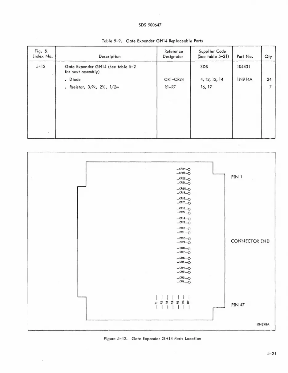
Fig. & Index No.
5-12
SDS 900647
Table 5-9. Gate Exponder GH14 Replaceable Parts
Description
Gate Expander GH14 (See table 5-2 for next assemb Iy)
Diode
Resistor, 3.9k, 2%, 1/2w
Reference Designator
CR1-CR24
Rl-R7
- CR24-o - CR23-o _ CR22 -o _CR2I-<)
_ CR20-o _CRI9-<)
_ CRI8-o _ CRI7-o _ CRI6-o _CRI5-<)
- CRI4-o _ CR13-o _ CRI2 -o -CRII-o
-CR10-o _ CR9-o _ CR8 --o _ CR7-o
_ CR6-o _ CR5 --o - CR4 -o _ CR3 -o _ CR2-o _CR1-o
I I I I I I I 0: &! ~ ~ !£ ~ ~ I I I I I I I
Suppl ier Code (See table 5-21)
SDS
4, 12, 13, 14
16, 17
"-
Part No. Qty
104431
1N914A 24
7
,-
PIN 1
CONNECTOR END
PIN 47
l04298A
~----------------------------------------------------------------------------------------.--.-
Fi~Jure 5-12. Gate Expander GH14 Parts Location
5··,21
SDS 900647
Table 5-10. Diode Gate No. 1 GK51 Replaceable Parts
Fig. & Reference Suppl ier Code Index No. Description Designator (See table 5-21) Part No. Qty
5-13 Diode Gate No. 1 GK51 (See tables 5-1 SDS 100246 and 5-2 for next assemb I y)
Diode CR1-CR36 4, 13 1N907A 36 4, 12, 13, 14 1N914A 4,6 1 N3063 4 1 N3065
. Resistor, 3.9k, 2%, 1/2w R1-R9 16, 17 9
- R9 - _CR36 -0 _CR35 -0 PIN 1 _CR34 -0
R8 ~CR33_
- - _CR32 -0 _CR31 -0
~CR30 _
_ CR29 -o _ CR28 -o ~ CR27 _
_ CR26 -o _CR25 -0
~CR2'L
_ R7 -_ CR23 -o _ CR22 -o - CR21 -0 ~ CR2Q.
_ R6 - _CRI9 -0 _CRI8 -0
CONNECTOR END _CR 17 -0
- R5 -o-CRI6 _
_CRI5 -0 _CRI4 -0 _CRI3 -0
_ R4 - 0- CRI2_
_CRII -0 _CRIO -0
_ R3 - 0- CR9 -
_CR8 -0 - CR7 -0
_ R2 -~CR6 _
_CR5 -0 _CR4 -0
RI 0- CR3 -
- - _CR2 -0 PIN 47
_CRI -0
l00243A
Figure 5- 13. Diode Gate No. 1 GK51 Parts Location
5-22
SDS 900647
Table 5-11. Data Amplifier HX29 Replaceable Parts
Fig. & Reference Suppl ier Code Index No. Description Designator (See tab Ie 5-21) Part No. Qty
5-14 Data Ampl ifier HX29 (See tab Ie 5- 1 SDS 103387 for next assembly)
Capac itor, mylar, 4700 pf, 10% Cl 23,25,191, 192, 193
Capac itor, mylar, 0.01 f-lf, 10% C2 23,25,191, 192, 193
Capacitor, mylar, 2200 pf, 10% C3,C5 23,25, 191, 2 192, 193
Capacitor, tan tal um, 4.7 f-lf, 20%, 50v C4 1 1, 22, 23, 24, 192,202
Capacitor, tan tal um, 47 f-lf, 20%,20v C7,Cll 11,22,23,24, c-~l
i thru C 14 192,202 I
Capacitor, mica, 39 pf, 5% C8 19,20, 188, 189
Capacitor, mylar, 0.015 f-lf, 10% C10 23,25, 191, 192, 193
Diode, SDS 103 CRI-CR5 3,5,10,11, 1N914A 5 14,225
Diode, SDS 101 VRI-VR3 1, 1 1, 14, 269 1N746 3
Diode, SDS 106 VR4-VR13 I, 10, 11, 14 1N752 10
Inductor, molded, 10 mh Ll 41,70,90,91
Integrated circuit, SDS 302 Al 3
Potentiometer, 2k R6, R31, R34 35,36 3
Potentiometer, 20k RlO 35,36
Resistor, 470 ohms, 2%, 1/2w Rl, R51, R53 11,16,17, 3 36, 176
Resistor, 68 ohms, ~Io, 1/2w R2 11,16,17, 36, 176
Resistor, 10k, 2%, 1/2w R3, 5, 14, 16, 11,16,17, 13 19, 33, 38, 39 36, 176 40,41
Resistor, 1k, ~/o, 1/2w R4, 7, 8, 11, 16, 17, 5 29,37 36, 176
Res istor, 270k, 2%, 1/2w R9 11,16,17, 36, 176
Resistor, lOOk, ~/o, 1/2w R11,46 11,16,17, 2 36, 176
Resistor, 47 ohms, 2%, 1/2w R12 11,16,17, 36, 176
Res istor, 3.3k, 2%, 1/2w R13,32 11,16,17, 2 36, 176
Resistor, 1.8k, 2%, 1/2w R15,28 11,16,17, 2 36, 176
--
5-23

SDS 900647
Table 5-11. Data Amplifier HX29 Replaceable Parts (Cont.)
Fig. & Reference Suppl ier Code Index No. Description Designator (See tab Ie 5-21) Part No. Qty
5-14 Resistor, 4.7k, 2%, l/2w R17, 18,20, 11, 16, 17,36, 9 (Cont.) 27,30,42, 176
48,49,50
Resistor, 8.2k, 2%, l/2w R21-R24 1 1, 16, 1 7, 36 4 176
Res istor, 39k, 2%, l/2w R25 1 1, 16, 1 7, 36, 1 176
Resistor, 22k, 2%, l/2w R26 1 1, 16, 1 7, 36, 1 176
Resistor, 10k, 2%, l/2w R35,36,43 1 1, 16, 1 7, 36, 3 176
Res istor, 220 ohms, 2%, l/2w R44, 52, 54 11,16, 17, 36, 3 176
Res istor, 27k, 2%, l/2w R45 11,16,17, 36,176 1
Res istor, 6.8k, 2%, l/2w R47 1 1, 16, 1 7, 36, 1 176
Transistor, SDS 205 Ql,2,5,6, 1,3,96 2N930 0 7,8,12,13 14
Trans istor, SDS 214 Q4, 11 1,3 2N2801 2
Trans istor, SDS 203 Q9, 10, 15 1,3, 11 2N2219 3
5-24

R36
R37
R35
R41
~o
SDS 900647
-(.)
RI 6
I len
II:
~ ~ I I
PIN 1
CONNECTOR END
PIN 47
1073848
~---------------------------------------------------------------------------------------------------------------------.-
Figure 5-14. Data Ampl ifier HX29 Parts Location
5-25

SDS 900647
Table 5-12. Read Ampl ifier HX30 Replaceable Parts
Fig. & Reference Suppl ier Code Index No. Description Designator (See table 5-21) Part No. Oty
5-15 Read Amplifier HX30 (See table 5-1 for SDS 107370 next assembly)
Capacitor, tantalum, 47 flf, 20%,20v Cl,C2 11, 22, 23, 24, 2 192,202
Diode, SDS 104 CRl 3,5, 14,63 IN3600 4
Diode, SDS 103 CR2,CR3 3,5,10,11, IN914A S .14,225
Diode, SDS 106 VRI-VRS 1,10,11,14 IN752 14
Resistor, 5.6k, 2%, l/2w Rl 11, 16, 17, 4 36, 176
Resistor, 39k, 2%, l/2w R2-R4 11,16,17, 12 36, 176
Res istor, S2k, 2%, l/2w R5, RS 11,16,17, S 36, 176
Resistor, 100 ohms, 2%, l/2w R6, R7 11, 16, 17, S 36, 176
Res istor, 15k, 2%, l/2w R9, RI0 11, 16, 17, S 36, 176
Resistor, 1. 2k, 2%, l/2w Rl1 11, 16, 17, 1 36, 176
Resistor, 910 ohms, 2%, l/2w R12 11, 16, 17, 1 36, 176
Resistor, 75k, 2%, l/2w R13 11,16, 17 1 36, 176
Resistor, 6. Sk, 2%, l/2w R14 11, 16, 17 1 36, 176
Res istor, 470 ohms, 2%, l/2w R15 11, 16, 17 1 36, 176
Transistor, SDS 201 01 1,3,5 2N2369 4
Transistor, SDS 205 02-05 1,3,96 2N930 13
5-26
R9-4
-y'R2:.it> _RI-~
2 4 - 4_
_R2-4_
o-£.RI-.i.. _R3-~_
....Jl 9 -L. -YR2~
_RI-3_
2 4 - 3_
_R2-L
~RI:~ _R3-?:-
_R9-2.-_
-YR2:£..r> ~I-L
_R4-2_
R2-?:-
Q-?I-.L _R3-!_
_R9-1_.
...::!.R2:J..r>
_RI-L
_R4-L
_R2-1._
o£.RI~L
SDS 900647
_R8-~
_R7-L
_R6-~
_R5-~
-Y 8 -L _R7-L
-Y 6 -L _R5-L
_R8-L
_R7-L
_R6-L
_R5-L
_RS-L
_R7-L
_R6-L
_R5-L
~o
~o
~O
~O
~O
~O
~O
~O
Figure 5-15. Read Ampl ifier HX30 Parts Location
PIN 1
CONNECTOR END
PIN 47
l07364A
5-27
SDS 900647
Table 5-13. Gate Write Amplifier HX31 Replaceable Parts
Fig. & Reference Supplier Code Index No. Description Designator (See tab Ie 5-21) Part No. Qty
5-16 Gate Write Ampl ifier HX31 (See tab Ie 5- 1 sDS 107429 for next assembly)
Diode, SDS 103 CR1-CR11 3,5, 10, 11, 14, 1N914A 44 225
Diode, sDS 101 VR1, VR2 1, 11, 14,269 1N746 8
Resistor, 5.6k, 2%, 1/2w R1, R2 11, 16, 17,36, 8 176
Res istor, 39k, 2%, 1/2w R3, R4 11, 16, 17,36, 8 176
Res istor, 1.2k, 2%, 1/2w R5, R6 11, 16, 17,36, 8 176
Transistor, sDS 203 Q1, Q2 1,3, 11 2N2219 8
_R4-~ ~O PIN 1 .fr .;r "r9 19 19 .p 11 "rl 11 1919 vi vi r--
_R3-4 - N_ -Vf'-NO'>Q=If)<.D I I
O£R3-~ C!: C!: C!: C!: C!: C!: C!: C!: C!: C!: C!: <.D If)
_RI-4_ ;0 >1 >1 UI ul ul UI u6 6 u6 UI UI C!:I C!:I
o-CRB:.i _R2-4 _
_ R4-3
~O -.fl3- 3 ~f ~~ rn9 ~9 ~9~? ,:,1 ~I ,:,1 ~9~9 ) ,:,1 oSR3:l. N - ~ V f'- N 0'> Q = If) <.D I C!: C!: C!: C!: C!: C!: C!: C!: C!: C!: C!: <.D If) RI-3
~O >1 >1 UI ul ul ul 06 u6 6 UI UI C!:I C!:I
oSRB-l..
R2-3_
R4-2_ CONECTOR END
_R3-2_ ~O N~ N~ N9 N9 N9 N9 N9 ~9 ~ cS? N9 1 ,;,,1 o-fR3:£. N.L~~~NmQ~J.,~~
_RI-2_ C!: C!: C!: C!: C!: C!: C!: C!: C!: C!: C!: <.D If)
cPRB =.£
~O >1 >1 ul ul ul UI ul ul ul ul ul C!:I C!:I
_R2-2 _
_ R4-1 -
- R3-1 - ~O oSR3-.L ;t ,~ ,9 ~ ,9 ~ ,9 -R ,9 ;? ,9 _I _ Rf-I_
~a:ii:~~~~~~:£~~ If) o-fRB:L
~O >1 >1 UI ul ul UJ ul ul ul ul UI C!:I C!:I
- _R2-1_
PIN 47
l07426A
Figure 5-16. Gate Write Amplifier HX31 Parts Location
5-28

SDS 900647
Table 5-14. Photo Sense Amplifier HX48 Replaceable Parts
Fig. & Reference Supplier Code Index No. Description Designator (See tab Ie 5-21) Part No. Qty
-
5-17 Photo Sense Amplifier HX48 (See table 5-1 SDS 117696 for next assembly)
Capacitor, tantalum, 2.2 fJf, 20%,50v Cl 11,22,23,24, 4 192,202
Capacitor, tantalum, 1 fJf, 20%, 50V C2,C3 11,22,23,24, 2 192,202
Diode, SDS 107 CR1,CR6 3,28,225 lN921 8
Diode, SDS 103 CR2, CR5 3,5,10,11, lN914A 8 14,225
Diode, SDS 101 VR1, VR2 1,11,14,269 lN746 8
Diode, SDS 106 VR3-VR5 1, 10, 11, 14 lN752 3
Potentiometer, 50k Rl 35,44,45 4
Potentiometer, 100 ohms R16 35,44,45 1
Resistor, 1.2k, 2%, l/2w R2 11, 16, 17,36, 4 176
Resistor, 33k, 2%, l/2w R3 11, 16, 1 7, 36, 4 176
Res istor, 10k, 2%1. 1/2w R4 11, 16, 17,36, 4 176
Resistor, 560 ohms, 2%, l/2w R5 11, 16, 17,36, 4 176
Resistor, 68k, 2%, l/2w R6, R7 1 1, 16, 1 7, 36, 8 176
Res istor, 2.2k, 2%, l/2w R8, Rll 11, 16, 17,36, 8 176
Resistor, 12k, 2%, l/2w R9, Rl0 11, 16, 17,36, 8 176
Resistor, 1.5k, 2%, l/2w R12, R13 11, 16, 17,36, 2 176
Res istor, metal fi 1m, lk,2%, l/2w R14 11,23,36,45, 1 73, 176, 185, 234
Res istor, 270 ohms, 2%, l/2w R15 11, 16, 17,36, 1 176
Res istor, 220 ohms, 2%, l/2w R17 11, 16, 17,36, 1 176
Res istor, 120 ohms, 2%, l/2w R18 11, 16, 17,36, 1 176
Resistor, metal film, 18 ohms R19-R22 11,23,36,45, 4 2%, l/2w 73, 176, 185, 234
".,.
5-29

SDS 900647
Table 5-14. Photo Sense Ampl ifier HX48 Replaceable Parts (Cont.)
Fig. & Reference Suppl ier Code Index No. Description Designator (See table 5-21) Part No. Qty
5-17 Transistor, SDS 205 Q1 1,3,96 2N930 4 (Cont. )
Trans istor, SDS 202 Q2, Q3 1,3,5,7 2N914 8
Transistor, SDS 214 Q4 1,3 2N2801 1
Transistor, SDS 210 Q5, Q6 3,8, 141 2N2890 2
PIN 1
CONNECTOR END
-~ .:c: =1 =========== PIN 47
~L..I _____ ...J
117693A
Figure 5-17. Photo Sense Ampl ifier HX48 Parts Location
5-30

SDS 900647
Table 5-15. AND/OR Inverter IHlO Replaceable Parts
Fig. & Reference Suppl ier Code Index No. Description Designator (See table 5-21)
5-18 AND/OR Inverter IH10 (See tables 5-1 SDS and 5-2 for next assembly)
Capacitor, tantal um, 4.7 !-If, 20%,50v C1 23,77
Diode CR1-CR23 4, 12, 13, 14
Diode VR1 2, 12, 13, 14
Res istor, 820 ohms, 2%, l/2w R1 16, 17
Resistor, 3.9k, 2%, l/2w R3-R10 16, 17
Resistor, 18k,2%, l/2w R2 16, 17
Transistor, SDS 201 Q1 1 3, 11
RIO ~R23-o
RI-4 - -.J;R22-o 01
~O (\J
0:: ~R21-o
~ -.J;R19-o _R2-L -.J;R18-o
RI-3_ ~R17-o
_R2-L ~R16-o
~O -CR15-o
"fl ~R14-o
1r R9 >6 ~R13-o
R8 _VRI-l..o
_R7_
_ R6_ ~R12-o ~RII-o
R5 ~R9-o
_ RI-2_ « -.J;R8 -o _R2-2_ 0 .sR7 -0
1r JR6-o
~O u,
_ CR5-o JR4::-a
R4 _VRI-~ _ CR3-o
_ R2-1_
~O _ CR2-o
_VRI:.Lo _R3 _ _CRI-o
_ RI-I_
0- CI
Figure 5-18. AND/OR Inverter IH10 Parts Location
Part No.
100137
1N914
1N746
2N2501 2N2369
PIN 1
Qty
23
4
4
8
4
4
CONNECTOR END
PIN 47
100134B
5-J1

SDS 900647
Table 5-16. OR Gate Inverter IHll Replaceable Parts
Fig. & Reference Supplier Code Index No. Description Designator (See table 5-21) Part No. Qty
5-19 OR Gate Inverter IH11 (See table 5-2 SDS 100319 for next assembly)
Capacitor, tantalum, 4.7 fJf, 20%,50v C1 23,77 1
Diode CR1-CR52 4, 12, 13, 14 1 N914A 52
Diode VR1 2, 12, 13, 14 1N746 4
Resistor, 820 ohms, 2%, l/2w R1 16,17 4
Resistor, 18k, 2%, l/2w R2 16,17 4
Resistor, 3.9k, 2%, l/2w R3- R28 16, 17 26
Transistor, SD S 200 Q1 1,5,7,95 2N834 4
RI3 o-CRII_ _ CR2.L..o _ CR2'-o _ R12_ o-CRIO_ _ CRI9-o _CR2Q...o PIN 1
RII o-CR9_ _CRIB-{)
r-- RIO o-CRB_ _VRI-.1..o
_ R9_ o-CR7 _ _VRI-2....0
RB o-CR6_
_R2-4 - o-CR5_ _ CRI7-o
O~ R7
_RI-4 R6 o-CR4_ _CRIELo
-o-CR3_
_ CRI5-o _R5 _ _CRI4-{)
o-CR2 _ _ R2-3_
O~ _R4 _
_CRILo R3
o-CRI_ _CRI2-{)
RI-3_ o-CR3L R2B _CR5LQ
CI R27 o-CR3L _ CR5I-o
cr- o-CR3L _ CR5<l...o
R26 _CR4~ CONNECTOR END RI-2_ o-CR3L
O~ R25
_CR4fLo _R2-2_ R24
o-CR3L
o-CR3L _CR4Lo R23 _CR4§..o
RI-I
O~ R22
o-CR31_ _CR4~ -
o-CR3~ _ CR41...o _R21_
R2-1_ o-CR2L _CR4~ _R20_
_RI9_ o-CR2/L
RIB o-CR2L
RI7 o-CR2L _VRI-'-o
RI6 o-CR2§..... _VRI-!...o
~R4Lo
- _RI5_ o-CR2L _ CR4 '-o _CR4~
RI4 o-CR2L _CR3~ _ CR3e....a PIN 47
l00136A
Figure 5-19. OR Gate Inverter IH11 Parts Location
5-32

Fig. & Index No.
5-20
SDS 900647
Table 5-17. AND Inverter IH12 Replaceable Parts
Description
AND Inverter IH12 (See table 5-2 for next assembly)
Capacitor, tantalum, 4. 7 fJf, 20%, 50v
Diode
Diode
Resistor, 3. 9k, 2%, 1/2w
Resistor, 820 ohms, 2%, 1/2w
Resistor, 18k, 2%, 1/2w
Transistor, SDS 209
-
R7-2 CR4-~ 1-~RI2-~_ -CRII-2-o t _R8-2_ QN l R12-2 ~
R5-2 CR3- -0 ~ cYRIO-'-. -CR9-2-Q-
_RG-2_ QN RII-2 ,;,
_ -;3-2 _ - ~R2- -00
(f. ~R8-~ -CR7-2-Q~
- R4-2._ DN Il:: RIO-2 N ,..
RI·2 _ - ,J:RI· -00
.b.. o-CRG-2._ -CR5-2-QT
- R2-2 - QN ~ _ R9-2 _ i; ,..
_ R7·1 _ ~R4- -0 .¢. ~RI2.'-- .J:RII-I-o~
R8·1.:.. 0 0:I ~ R12-1 " I
_ R5-1 _ .£R3-I-o /\
ofRIO-L SR9.I-oT
RG-I O-,J, _ ~II-1 _-- ~ t
_ R3-1 _ SR2-I-o ~
o-CR8 -'-_ -CR7- I-o;t _R4-1 -- 0- Il:: I >
_RIO-I_ ~ 1
- RI·I - SRI·I -0 Lf o-C RG- I_ -CR5-I-o,
_R2-1 - 0 a: - > - R9-1 _ i; I
Reference Designator
C1
CR1-CR29
VR1-VR10
R1,3,5,7, 13, 14, 17, 19,21,23,26
R2, 4, 6, 8, 15 18,20,22,24, 25
. R9-R12, R16, R27 - R30, R41
Q1-Q10
RI7 CRI7 -0 ~
o-CR23- -CR22-o1O
--_-;::R~18~_ 010 g; _ R27 _ 0 I
- RI9 - -CR18 -0 t::. o-CR25- -CR24-Q,....1
--_~R~2~O-_ 0 g; ~ I _ R28 _
- R21 - -CRI9-o ~ o-CR27- -CR2G-ooo
--_--R;;;;,2,..,;:2:.:..:.;_ 0 Il::
00 ~ _ R29 _ 0
SR20-Q~ _ R23 _ SR28-o
en ____ Q-C:;"....-R29- g;
_R24 - 0 I _ R30 _ ~
_ R2G - _CR21 -o~
-R25 - Oo~ _ R31 _ 0>1
- RI4 _ -CRIG-o
RI3 SRI5 --01 I
RIG O~ If)
- _R15 - - ~6 5 II I _YR' -{> 8 '"
Figure 5-20. AND Inverter IH12 Parts Location
Suppl ier Code (See table 5-21)
SDS
23,77
4, 12, 13, 14
2, 12, 13, 14
16, 17
16,17
16, 17
1 3 7
-- --
Part No. Qty
101767
1
1N914A 41
1N746 14
15
14
14
2N2538 14 2N2848 2N2476 ""---
PIN 1
CONNECTOR EN D
PIN 47
l01537A
5-33
SDS 900647
Table 5-18. Inverter Amplifier IK51 Replaceable Parts
Fig. & Reference Suppl ier Code Index No. Description Des ignator (See table 5-21) Part No. Qty
5-21 Inverter Ampl ifier I K51 (See tab les 5-1 SDS 100388 and 5-2 for next assembly)
Capacitor, silver mica, 68 pf, 5% Cl-C4 19,20,21 9
Capac itor, tantalum, 4.7 fJf, 20%,50v C5 23,77 1
Diode CR1-CR10 4, 12, 13, 14 lN914A 16
Diode VR1-VR6 2, 12, 13, 14 lN746 15
Resistive Termination Assy, 3 ea ATl-AT4 72 56-590- 11 65/3B
Resistor, 820 ohms, 2%, l/2w Rl,3,6, 16, 17 13 9,12
Resistor, 18k, 2%, l/2w R2, 4, 7, 16,17 13 10,15
Res istor, 3.9k, 2%, l/2w R5, 8, 26 16,17 6
Resistor, 560 ohms, 2%, l/2w Rl1,13, 16, 17 16 16,17,19, 20,21
Resistor, 10k, 2%, l/2w R14 16,17 3
Resistor, 470 ohms, 2%, l/2w R18 16,17 2
Res istor, 15k, 2%, 1/2w R22 16,17 2
Res istor, 27k, 2%, 1/2w R23-R25 16, 17 6
Transistor, SDS 201 Ql-:Q8 1 2N2501 20 3,11 2N2369 95 2N2710
5-34
_R26-2 _
_ R21-2 _
_ R20-2_
_R20-1 _
_ R21-1 _
_ R26-1 _
_ R24-1_
SDS 900647
PIN 1
CONNECTOR END
PIN 47
1003858
~-------------------------------------------------------------------------------------------------------.-- -Figure 5-21. Inverter Amplifier IK51 Parts Location
Table 5-19. Relay Driver RK53 Replacement Parts
Fig. & Reference Suppl ier Code Index No. Description Designator (~;ee table 5-21)
5-22 Relay Driver RK53 (See table 5-1 for SDS next assembly)
Capac itor, mylar, 3300 pf, 5% Cl, C4 26,27,74
Capacitor, mylar, 4700 pf, 5% C2,C3 26,27,74
Capacitor, tantalum, 4. 71-1f, 5% C5 22,23,77
Diode CR1, CR4 4, 13 thru CR9 4, 12, 13, 14
4,6 4
Diode CR2, CR3 13, 15,28
Part No.
100905
lN907A lN914A lN3063 lN3065
lN921
--
Qt y --
2
8
8
8
8
8
5-35

SDS 900647
Table 5-19. Relay Driver RK53 Replacement Parts (Cont.)
Fig. & Reference Suppl ier Code Index 1'-10. Description Designator (See table 5-21) Part No. Qty
5-22 Diode, Zener VRl 2, 13, 14,32 lN746 4 (Cont. )
Resistor, 47k, 2%, l/2w Rl, R7 16,17 8
Resistor, 3.9k, 2%, l/2w R2 16,17 4
Res istor, metal film, 100 ohms, 1%, lw R3 36,38,73 4
Res istor, metal film, 68 ohms, l%,lw R4 36, 38, 73 4
Res istor, 22k, 2%, l/2w R5, R6 16,17 8
Res istor, 4.7k, 2')0, l/2w R8 16,17 4
Transistor, SDS 203 Ql-Q3 1 2N2219 12 29 2N2404
v v _ CI-4 _ _ R5-4 _ ,!., N
_CRS-4-o 0 0
_CR2-4-o I 0 0 1 _CR9-4-o "f N _VRI-4 --t>
_ RS-4_ 10 U r-- r "7 0::
v r<> I~ I o-CR4-4_
r _R7-4_ 0:: 0:: _CR7-4-o 1i: r<>vO _ C4-4_
_CR6-4 -o lo-CRI-4- 5 .!.. 1 0 _ C3-4 _ _CR5-4 -o
_ R2-4_
PIN 1
r<> '0 _CR8-3 -o _ R5-3_ ;g N _ CI-3 - 0 _CR9-3-o
_CR2-3-o r<> 0 0 r<> _ VRI-3-{>
tD N o-CR4-3_
I _ R8-3_ r<> '? 0::
19 u _CR7-3-o
'? .;- r<>
_CR6-3-o R7-3 0:: 0::
~~O 1i: - C4-3 _ _CR5-3-o lo-CR'-3_ 0:: ,
'lo _CRB-2 -o _ R2-3_ _ C:3-3 _
:h N _CR9-2-o
_ CI-2_ _ R5-2 _ N 0 0 _ VRI-2 -{>
I 0 0 <;J o-CR4-2_ _CR2-2-o N
C}J u _CR7-2-o 10
_ R8-2_ N ~ 0:: _CR6-2-o
~ .t r<> 19 _CR5-2-o _ R7-2_ 0:: 0::
~ruo 1i: C4-2 _CR8- I-o lo-CRI-2- ~5
_ R2-2_ _ C3-2 _ _CR9-I-o ;;:; N
_VRI-I -[> _ CI-I_ _ R5-1_
0 0 o-CR4-1 _
CONNECTOR END
_CR2-1 -0 0 0 _CR7-I -o
.b N _CR6-I-o u
_ RS-I_ 0:: _CR5-I-o .;- ,;, 19 I _ R7-1_ 0:: 0::
0:: ,;,
~O _ C4-1_
i....-- I o-CRI-I - 0::
'--l _ C3-1 _ _ R2-1_
- C5 -0 PIN 47
100902B
Figure 5-22. Relay Driver RK53 Parts Location
5-36

SDS 900647
Table 5-20. Digital-to-Staircase Converter SK58 Replacement Parts
Fig. & Reference Suppl ier Code Index No. Description Designator (See tab Ie 5-21) Part No. Qty
5-23 Digital-to-Staircase Converter SX58 (See SDS 109413 table 5-2 for next assembly)
Capacitor, tantalum, 4.7 f-lf, 20%,50v Cl, C2 11,22,23,24, 2 192,202
Diode, SDS 103 CR1-CR24 3,5,10,11, 1 N914A 24 14,225
Resistor, 180 ohms, 2%, l/2w Rl 11, 16, 17,36, 176
Resistor, 18k, 2%, l/2w R2-R4 11, 16, 17,36, 3 176
Resistor, 8.2k, 2%, l/2w R5- R13 1 1, 16, 1 7, 36, 9 176
Resistor, 560 ohms l , 2%, l/2w R14-R16 11, 16, 17,36, 3 176 . Resistor, 33k, 2%, 1/2w R17-R19 1 1, 16, 1 7, 36, 3 176
5-37
5-38
SDS 900647
COMPONENT LOCA nON
CAPACITORS
C 1 (24 1 ~{- 240)C2 (238 ~(- 237)
DIODES
CR 1 (27 -f+ 74)CR2(25 +4- 72)
CR3(24 +4- 71)CR4(23 +4- 70)
CR5(22 -f+ 69)CR6(21 +4- 68)
CR7(19 +4- 66)CR8(17 +4- 64)
CR9(16 +4- 63)CRlO(15 -f+ 62)
CRll (14 -f+ 6l)CR12(13 -f+ 60)
CR13(12 -f+ 59)CR14(11 -f+ 58)
CR 15(7 -f+ 54)CR 16(5 -f+ 52)
CR17(4 -f+ 5l)CR18(3 -f+ 50)
CR19(2 -f+ 49)CR20(l -f+ 48)
C R21 (30 -f+ 77)C R22 (29 -f+ 76)
CR23(10 -f+ 57)CR24(9 -f+ 56)
192 149 100 193 150
194 151 102 195 152
196 153 104
r--- 197 154 198 155 106
199 156 200 157 108
201 158 202 159 110 143 144
203 160 204 161 112
205 162 206 163 114
207 164 208 165 116
209 166 210 167 118
211 168 212 169 120
213 170 214 171 122
215 172 216 173 124 145 146
217 174 218 175 126
219 176 220 177 128
221 178 222 179 130
223 180 224 181 132
225 182 226 183 134
227 184 228 185 136
229 186
48
50
52
54
56
58
60
62
64
66
68
70
72
74
76
78
80
82
84
230 187 138 147 148 86 . 231 188
232 189 140 88 233 190
234 191 142 90
101
103
105
107
RESISTORS
R5(194-151 )R6(196- 153)
R7(198-155)R8(206-163)
R9(208-165)RlO(21O-167)
R11 (214-171)R12(216-173)
R13(218-175)
R14(197-154)R15(209-166)
R16(217-174
R18(200-157) R 17(202- 159) R 19(220- 177)
I 49 2
3 51 4
5 53 6
7 55 8
9 109 57 10
II III 59 12
13 113 61 14
15 115 63 16
17 117 65 18
19 119 67 20
21 121 69 22
23 123 71 24
25 125 73 26
27 127 75 28
29 129 77 30
31 131 79 32
33 133 81 34
35 135 83 36
37 137 85 38
39 139 87 40
41 141 89 42
43
92 91 44 94 93 45 96 95 46 98 97 47
99 235 236 237 238 239 240 241 242
243 244 245
Figure 5-23. Digital-to-Staircase Converter SX58 Parts Location
PIN 1
CONNECTOR END
PIN 47
100611
Code No.
2
3
Name
Motorola Sem iconductor
Same as 1
Fairchild Semiconductor
4 Same as 3
5
6
7
8
10
11
12
13
14
15
16
17
19
20
21
22
General Electric Co. Sem iconductor Products Div.
Same as 5
RCA Sem iconductor D iv.
Sil icon Transistor Corp.
Hughes Sem iconductor Div.
Texas Instruments, Inc.
Same as 11
Pacific Sem iconductors, Inc.
Continental Device Corp.
Sperry Sem iconductor Div.
Corn ing Glass Works
Welwyn International, Inc.
Arco Electronics, Inc.
Sangamo Electric Co.
Micamold Electric Mfg. Co.
Kemet Company
SDS 900647
Table 5-21. Supplier Code Index
Address
5005 E. McDowell Rd. Phoen ix, Arizona
545 Wh isman Road Mountain View, Calif.
Electron ics Park Syracuse 1, N. Y.
Somervi lie, N. Y.
East Gate Blvd. Garden City, N. Y.
500 Superior Ave. Newport Beach, Cal if.
P.O. Box 5012 Dallas, Texas
1420 Aviation Blvd. Lawndale, Calif.
12515 Chadron Ave. Hawthorn, Cal if.
380 Main Ave. Norwalk, Conn.
550 High St. Bradford, Penn.
3535 Edgecl iff Terr. Cleveland 11, Ohio
Commun ity Drive Great Neck, N. Y.
1207 N. 11th St. Sprin~lie Id, III.
65 Gouverneur St. Newark, N. J.
11901 Madison Ave. Cleveland 1, Ohio
Code No.
23
24
25
Name
Sprague Electric Co.
U. S. Semiconductor Products
General Electric Co. Capacitor Dc?pt.
Address
481 Marshall St. North Adams, Mass.
3540 W. Osborn R. Phoen ix, Ariz.
Hudson Falls, N. Y
26 Same as 23
27
28
30
35
36
38
41
42
44
45
48
49
51
53
55
63
Same as 23
Raytheon Semiconductor 350 Ellis St. Co. Mountain View, Cal if.
General Instrument Corp.
Bourns, Inc.
65 Gouverneur St. Newark, N. J.
1200 Columbia Ave Riverside, Calif.
International Resistance 401 N. Broad St. Co. Philadelphia, Penn
Same as 23
Delevan Electronics Corp.
Same as 41
Atohm Electron ics
Dale Electron ics, Inc.
Littelfuse, Inc.
Bussman Mfg .. Co.
C inch Jones Division
Ohmite Mfg. Co.
Centralab
Transitron Electronic Corp.
77 Olean Road East Aurora, N. Y.
7648 San Fernando Roud Sun Valley, Cal if.
P. O. Box 609 Col umbus, Nebraska
1865 Miner St. Des Plaines, Illinoi
Un iversity at Jefferson St. Louis, Missouri
1026 S. Homan Ave. Chicago, III.
3635 Howard St. Skok ie, I II inois
900A E. Keefe Ave Mi Iwaukee, Wisc.
168-182 Albion St. Wakefield, Moss.
5-:39

Code No.
63
68
70
72
73
74
76
77
80
81
82
84
90
91
95
96
100
106
Name
Transitron Electronic Corp.
Delta Semiconductors Inc.
Nytron i cs, Inc.
Ferroxcube Corp. of America
Electra Mfg. Co.
Same as 25
Same as 24
Same as 24
Same as 23
Same as 20
E leo Corporation
General Electric Co. Miniature Lamp Dept.
J. W. Miller Co.
Stanwyck Winding Co.
Philco Corp.
Amperex Electron ic Corp.
Same as 53
Arrow-Hart and Hegeman Electric
113 Controls Co. of America
138 Manitor Products, Inc.
5-40
SDS 900647
Table 5-21. Supplier Code Index (Cont.)
Address
168-182 Alibion St. Wakefield, Mass.
835 Production Place Newport Beach, Cal if.
550 Springfield Ave. Berkeley Heights, N. J.
E. Bridge Street Saugerties, N. Y.
4051 Broadway Kansas City, Mo.
Willow Grove, Penn.
Nela Park Cleveland 12, Ohio
5917 S. Main St. Low Angeles 3, Cal if.
137 Walsh Ave. Newburgh, N. Y.
Lansdale Division Lansdale, Penn.
230 Duffy Ave. Hi cksvi lie, N. Y.
103 Hawthorne St. Hartford, Conn.
9555 Soreng Ave. Sch iller Park, III.
815 Fremont Ave. South Pasadena Cal if.
Code No. Name
141 M inneapol is-Honeywell Semiconductor Products
160 Magtrol, Inc.
161 West Coast Electrical Mfg. Co.
162 Minneapol is-Honeywell Micro Switch Division
163 Eldema Corp.
164 Potter and Brumfield Div. of Amer. Machine and Foundry
165
166
167
Electric Indicator Company
General Instrument Co. Magne Head Division
Contract Tool Corp.
Address
27474th Ave. South Minneapol is, Minn.
241 Seneca Street Buffalo 4, N. Y.
233 W. 116th Place Los Ange les 61, Cal if.
Chicago and Spring St. Freeport, III.
1805 Belcroft Ave. EI Monte, Calif.
1200 E. Broadway Princeton, Indiana
Camp Avenue Stanford, Conn.
3216 W. EI Segundo Hawthorne, Cal if.
3820 Hoke Ave. Culver City, Calif.
176 Clarostat Mfg. Co. Inc. Washington St.
185
188
189
191
192
193
202
225
234
269
Mepco Inc.
Aerovox Corp.
Corne II-Dub i I ier
Dearborn Labs
TRW Capacitor, Div.
Electron Products
Dickson Elect. Corp.
National Transistor D iv. ITT
Key Resistor Corp.
International Rectifier
Dover, New Hampshire
35 Abbet Ave. Morristown, N. J.
740 Be II e v i II eAve. New Bedford, Mass.
50 Paris Street Newark 1, N. J.
Box 3431 Orlando, Florida
112 W. 1st Street Ogallala, Nebraska
1962 Walker Ave. Monrovia, Cal if.
31OS. Wells Fargo Scottsdale, Arizona
500 Broadway Lawrence, Mass.
321 W. Redondo Beach Blvd., Gardena, Calif.
233 Kansas St. E I Segundo, Cal if.

SDS 900647 Paragraphs 6-1 to 6-3
SECTION VI
DRAWINGS
6-1 GENERAL
6-2 This section contains reference drawings useful in servicing and maintaining the MAGPAK Tape System. Included are installation drawings (figures 6-1 through 6-3), logic diagrams for both Model 9446 and Model 9448
(figures 6-4 and 6-5), power distribution diagrams (figure 6-6), and schematic diagrams (figures 6-7 through 6-30).
6-3. To aid in finding signal sources on the logic diagrams, two signal-location charts (tables 6-1 and 6-2) are included. Table 6-1 shows signal locations for figures 6-4, and table 6-2 shows them for figure 6-5.
6-1

6-2
13 1.
~
$
I { I
0 0 0 0
@ C (@) @@@@
~
SDS 900647
0 0
~ ~
\
0 0 0 0
II i
~ @ @
~ @Q)@@
~ ~ -...
~Y
!3~ I
l J
/
f
tV/(J-.!Ji! NC-28 HT6 Ndt.£oS
\ ~ .S"e,/A""rAt:;~ ('rA6t.~., tClJI~v.)
TH;(J" AN"A nI lie ,~,. ~ AM' ,.~t1~
1\\1111 I
...0... -- -- - -
---~ ~~ e; Gil --~ ~I)-- -
"'9. Q
I I
f I I I I
I I '7. I I «r-
~
I I
I
I I I
I I I I I I I I I
I I t ~ I ~,lb~ 0)
- - .~ ~.J __ - - __ • .rt".;>~ ~ IJ .:,
~-1 -- - - . "11 r. I I J I -I I
trEAI I~·IJ 107798-3B
Figure 6-1. Model 9446 Installation, Table-Mounted

rr:-1fL-Ii ,---" I U
r ~\
II.M"
SDS 900647
/
o o
~
I r I I I
1
f I
I I
I I I!o___ _ _ --.AI ~-- A
..... --·------/7.4~--------- ...........
t ~\
/(J.SO ~c,r
If. 00
107798-1B
~--------.-------------------------------------------------------------------------.--
Figure 6-2. Model 9446 Installation, Rack-Mounted (Sheet 1 of 2)
6-3

SDS 900647
~ ~
"-~ ~ ~ \ )
~ ...: '" ~ ~
~ ~
----
I:
til -c " • c;:)'" ~ -c . ~~ 'I ~
~ ,,~ , ~~
\') i::: ~~ " 0\ ~ ~~ " Vj
107798-2B
Figure 6-2. Model 9446 Installation, Rack-Mounted (Sheet 2 of 2)
6-4
SOS 900647
--~
fj -----c ~,~
"'" .. "" ...
r CJ 0 CJ I
I~ I
I I
I I I I
I I
~ ~ I ,., ! I
I IA
I ~ lQ ~
I I
I I
I: :
0 I;:'~~,>-CJ 0 CJ
0 0
~'-
~ -.., -... I I I
I
, I !'I' : i: :1 :
Ii ;:~ : I 1
] ~~~
r ~
107331-1A
Figure 6-3. Model 9448 Installation (Sheet 1 of 2)
6-·5
MOL)ULe AREA
6-6
SDS 900647
IB.7B MAX
.-------------- 18.31 REF"
Pt/SH BI./TTON} lATCH . TYP
Ct//OE P/A/
21.aJ MAJ(
CLeARANCE r-OR Ala /0 AlTti SCREhJ'
DC CABLE
PBO
Figure 6-3. Model 9448 Installation (Sheet 2 of 2)
l07331-2A
SDS 900647
Table 6-1. Model 9446 Signal Location Chart (for use with figure 6-4)
Fig. 6-4 Fig. 6-4 Fig. 6-4 Signal Sheet No. Signal Sheet No. Signal Sheet No.
AANS 1 ETK2 2 LWN2 4
AANS 1,2 ETL 3,7 MAN1 1
AUT 3,7 ETLl 3 MAN2 2
AUn 3,4,5 ETL2 3 PLP1 3
AUT2 4 ETn 1 PLP2 3
BOR 7 ETT2 2 RDAS 5
BOTS 1,2 FPDl 1 RDA1 1,3
BOn 1,3,6 FPD2 2 RDA2 2,3
BOT1 1,3 FPNl 1 RDDl 5
BOT2 2,3,6 FPN2 2 RDD1 5
BOT2 3 FWDl 1 RDD2 5
BRK1 1 FWD2 2 RDD2 5
BRK2 2 LES 1 4 RDK 5,7
BTA 7 LES2 4 RDNl 5
BTK 7 LND1 3 RDN2 5
BTK1 1 LND2 3 RDN2 5
BTK2 2 LND2 3 RDR 5,7
BTL 7 LRDl 5 RDYS 1,2
BTLl 3 LRD2 5 RDY1 1,3
BTL2 3 LRNl 5 RDY2 2,3
CHSB 3,4,5 LRN2 5 REV1 1
CHSB 3,4,5 LTDB 3 REV2 2
DATA 4,5 LTDB 3 REWM 1,2
DATA 4 LTDl 1,3 REW1 1
EOR 7 LTDl 1,3 REW2 2
EOTS 2 LTD2 2 RHS 7
EOTS 1 LTD2 3 RNG 5,7
EOTl 1 LTNB 3 RNU 5,7
Eon 1,3 LTNB 3 SELP 4
EOT2 2 LTNl 1,3 SELS 4
EOT2 3 LTN1 1,3 SEL 1 1,4,5
ETA 7 LTN2 2 SEL2 2,4,5
ETAl 1 LTN2 3 STOP 1,2,3,4
ETA2 2 LWDl 4 STOP 3
ETK 7 LWD2 4 S12T 3
ETKl 1 LWNl 4 TFPS 1,2

SDS 900647
Table 6-1. Model 9446 Signal Location Chart (for use with figure 6-4) (Cont. )
Fig. 6-4 Fig. 6-4 Fig. 6-4 Signal Sheet No. Signal Sheet No. Signal Sheet No.
TFPS 1 TSB2 2,3,4 WDG1 4
TFP1 1 TSB2 4 WDG2 4
TFP2 2 T12S 1,2 WDW1 4
TSA1 1,4 WED1 4 WDW2 4
TSA1 1,4 WED2 4 WNB1 4
TSA2 2,4 WEN1 4 WNB2 4
TSA2 4 WEN2 4 WNY1 4
TSB1 1,3,4 WDAS 4 WNY2 4
TSB1 1,4 WDAS 4 WRTS 4
6-8

.'-16 MANI--<~ MANI
@ ROY' _34
TI2S-<~ 'I~ U-ZZ7-l1 -(~®
2fd3 RWAI
@SEL'
@STOP ,I I II ~~
\
29 ,,\'/' c-- TSA,
4'"12 ----"'-o--«+__
/~ ml Al .'-'4 ~'i O(~
~ STJiI III" I IIII h":t'
-0-
41-39 BTA[ -~ XI 0-1 14
3& --";'>(J CL
BTl( 4'-040 II
E T IO-----+~ 411111 -
ETA "'-4Z 18 [---+>0 304
~--+ XI o---i ETIC "1-43
I ~9J\ ,\7
3Z~J-----~ 8
TSBI
.r;@\ (l,113~
43
..._---TS8'
41-11 +--
--~"-- rnl r 41-13 o-<~
----lOTI I 41-19 I I 0 (+--
~~EOTt '--------31· .. ~~GND
RI<53 41-.. ..
@
~
~?' -,0-< +---F-W&f--" >0 0 8REWM!!Jo 26--" 27-4
@ROAI
OOENOTES SHEET NUMBER,
31
41-25
\' toTi
,;,,1;
"-.=> REFERENCE DESIGNATIONS ARE ABBREVIATED. PREFIX THE DESIGNATION WITH UNIT NUMBER
t .-ri;.()
OR ASS£MBL'f DESIGNATION OR BOTH. (MIL. STD. 16B)
'LTDI
."
CO C .., (J)
~ I ~
V1~ :J'"'o (J) 0... (J) (J) ....
--0 o ~ ..... ~ o--~
......... ..-o
CO o
o o
o CO '-J .., VI 0
~ ::1 I
FPDI
~
~LlS1
40 36 36 'COMMON £NA8~" r I:::. CARD POs. 36 I
@fijll 42 i
I
I
Motion Control logic (Unit 1)
1>' It _4>
.51 fY~
/-11 tlt. 31
J .. 1 t~10
Z _~50
)til'~1 ;' ~+-- aRKI
., 4J '27 '"'~a.~
1:)1
t 1; ~:o
~ ,~ 'f'R~I:Zt v I
~'O . -IF'\" _ Rf(F\ p,ti .
- 0 e"t..l" G.. pJP"'\1'" .
gw1rrrv 1 A... ~--\ , v--""'~,·· .... ,,·-
"0 0 t:- ~-
h--'-cb
VI o VI
-0 o o 0-. ../:>. '""-..I
cr- }> -0

0-I
o
MANZ -." "Z-16
ROYl (!) TI25 II ;;it) I I ±
2611 RWAZ± 110
- - VIA;;'I @SELZ I r-...
I 11 I!!....
.... - -- ._. - -- . -- . @sroP
, STft2
am o-=:--v~ 26-4 I AWP2 2fdO ;:::
~~.L,' (/'"/\ "
.v . '\ ( t" ()
~W_
• TSA2
,I I z_
MANI
filA;!
i !I'D 1· 42-14 • .-.. --~ ...
-----,9 ""II 32 ~5 "Z·" B" 0<"
TSI2 .-----ftD
>~
r< lei )i:I 0
'AI'WM TIR2 0 I I ''l·I3 1---0 D ( +'
~
27-4
ntt 4~'
ITA 4',39 '
C)O 24
ITO )0' :-4l-40 ~
ETf~~ nA "z..4Z -
C.>O 28
, . 0
, 38
ill STOP PIN 11
ZZ
~"DA2 0"4
tLToi
11
CO C @ 0-
I' .J:!>..
Vl~ :TO (1) 0-(1) CD -I" _
"'-.0 o t -1">0-
~r-o ~. o
9. o
CO ~ a ~ 3 -0 I
I'V »
lOTI
@TUn •
.-----IOTZ ';2-19
I I D ( .....
" I 1m ",. I I I I I 0<""011
28-1 2e-30& J!1 4l
COMMON ENAaU CAAD 'OSo.II
zz
16
Motion Control logic (Unit 2)
Z .... , Z9-4O &024 o D r ( ..
RI<53 4'-44
+50
I '3\ I • <+-NDl .42·25
'_~ I D (<E--' "'IYI 42-2a
'2
~ ; 11.<:- MW. 42..z4
~+-- IRKZ 42-Z7
6>
Vl o Vl
-.0 o o 0-.J:!>.. '-.J

~ ,\"l..i..
f" \'D . \ J. ./" ,\ , ........ .... ".:'. "', .l 11"'-
'" C • It"~
t' ~ ,
0"-I
~ I
I'V
'" "\ \~L.""
0
" <.n -I=>---0 I
w »
_.- -.
::: ::I'::,tl§iB~ ,~, L'TN"i (!) ruii" CD
LTN2-4> r-III A 9-f.) rni@
_ 4z.i! !~~ .fUi2@ LTOI-+ 4
40 UNI 04' 31 '::: ~'\"'!r";;.N
t'" 1~1{t\?
HSCI ,TST!
@)f)
38 " ~ .=oDO H(Sa
\ ,G '" (1''-' (!)SI2T
~ e,l"" 11\\ Q <DrlZS )
~r, .
.-------------:===========~ II 104. RDA! 1t ." - ~., 15" . > ~ i .... -~ ... , 0' ,...... ,...., AllY' Aura-.~ . ..". I • .;--..... ...... H .. ~ 13 LND2 _ •• _ _
~aTD2-------------------------------~----~
@BTS2
(!) TC;BI-AUTI-+> --41--I~,-r-7--
o - <r i
042
@BTSI 32
ml
i)81'DI iOTi
<D{BOTI --~---=-----=t:::==~ Eon
~{: I.
38 >---00-< ( BTL 1
41-18
15 )---0-0< ( ITL2
042-18
19 20 or,
STOP
H,9 -iOTz
ITP2 I
ID ~ Brrfi
....--t- gTPI
~ ~ 29 ETL o.<~ .. ,-eo~"'l5
~ fS ETL ~~
42-20 ~-+Z5
-n (0 c
8S12T~ 26-1 43-1~ ~~ 43--12 ~~ N 0
43-14
CLOCKWISE T}~ 8> STOP <D@
INCREASE 31 LAMP vOLTAG£ .... _I '. • 0' srAI(j)
STRZ@
~ a
PL'P'
~>-} ... -23 TO PHOTOSU~4iE LAMP(+ 2.50Y)
PL'Z
CD 0-I ~
.- -... Ul~ :::ro (I) 0... (I) CD -t- _
W-o o .po. ..... ~ 0-0--. o
co 0
n a
C'€ d 3
o 4Z'::it>-
Status/Select Logic
,.t';:·(~p
Vl o Vl
'0 a a ~ '-I

f~'(tU CHSB -----+--f---,~~
t:)OP ~----4-~~~
@8~,~TS--<
$£1...,. tJ9·J'
(j STOP
rsrz T'SBl
AUTI
LES 2
..---------J.--~ 26·
~-----~--~26
SDS 900647
10 LWOI
H)(-31 38,
S 41·30 WOWI
1---~6-';'~ 1--_-0.:2'---0< E-(----WEDI
'--__ --J "'-29
paz POS 16
le41-:3~
II 14 WSNI 16
LWNI HX-31
38 1-_~Z~O:....o41-<-:3~ 1---0-
':':"-0-< E-(---- WEN I
041·28
II 43
19
WS02 25
WSN2
'---L-W-O-2 --,1--_-o:=:3~1 _4~Z~.:30::JWOW 2
H)(-31 38 r-_-o.:;~::=-4-<ZK-31 WOGZ
r--""O---O<fE-(---- WE02 4Z-29
paz POSl7
r--~-~--~4~1~42~~2 WN82
LWN2 ;J HX-31 38 1--_--0-,4::;2,....4'02<-33 WNY2
1--_-0-:3:..:9:....0< +1( ------WEN Z 42-28
~-------------4_-------------------------~--- SELZ~
r-.9~ ______ ~~~
20 26-33 P84 26-37 1 SEL 5 ~>-oI~~O~P8-3-Z~~~-<:-<31 +-9SELS
>-~~ __ ...,....--------------_----.- SELI<D~
l j
I
I I
~ J T581 Data Tran.sfer logic (Write)
'--___________________ . __________________________________________ 1_07_5 __ 49-4~
Figure 6-4. Model 9446 Logic Diagram (Sheet 4 of 6)
6·13

I, REAOHDS
'2 READ HO'S
@OATA
SDS 900647
HX30 LRDI 45
LRNI .5
LRDZ
45
LRN2
4S .
DATA
20 @8WMS ------------------------------------------------------------~~~--~
Data Transfer logic (Read)
Figure 6-4. Model 9446 Logic Diagram (Sheet 5 of 6)
6-14
27-31
l07549-5A
BOT,~-·--~-l
BOT 2 --I..--~-I
SDS 900647
05 ----0
07 40-8 ~~=r~~--~BT02@
BTU'
1 P64 CI I 100 IJ fd-20 V
~ P84 C2 r'00,.,fd-20V
Delayed BOT Logic
~~_~o2 ______________ ~_3-~3~TSI@
l07549-6A
Figure 6-4. Model 9446 Logic Diagram (Sheet 6 of 6)
6-15

SDS 900647
Table 6-2. Model 9448 Signal Location Chart (for use with figure 6-5)
Fig. 6-5 Fig. 6-5 Fig. 6-5 Signal Sheet No. Signal Sheet No. Signal Sheet No.
AANS 12 CUG 9 RC 3
BOTS 12 CURD 8 RCP 4
BUC 14 CUS 7 11 RCRG 4
BUC 9 5 CUWD 8 RDA 3
CBG 6 C12M 11 RDYS 12
CECF 10 C12 14 REWM 12
CERF 11 C13 14 RF 3
CETF 10 C14 14 RG 3
CFMF 10 C15 14 ROOl 3
CHROO 6 C16 14 ROO2 3
CHROl 6 C170 14 RP 14
CHR02 6 C21 14 RSA 4
CHR02 6 C22 14 RSAB 5
CHR03 6 C23 14 R5A3 3
CHR04 6 ECM 5 R5B 4
CHR05 6 EOTS 12 RSC 4
CHR06 6 FC 1 R5C3 4
CNTL 12 GDA4 13 RSD 4
CSA 8 HRG 6 R5E 4
CSB 8 HROO 6 RSF 4
CSC 8 HROl 7 RSF3 3
C5G 9 HR02 7 Rl 14
CSOA 9 HR03 7 R2 14
C5RF 11 HR04 7 R3 14
CSO 9 HR05 7 R4 14
CSl 9 HR06 7 R5 14
CS2 9 IHGD 8 R6 14
C53 9 IOC 14 SEL5 10
C54 9 IOC 9 5 5FG 6
C55 9 LLT6 12 SPG 6
C56 9 LLT7 12 5RG 6
C57 9 MTG 5 5TOP 12
CS13 9 Q2 14 5TRT 12
C527 9 Q29 5 512T 12
C556 9 RABC 5 510 13
CUFF 11 RAB3 3 TE5T 4
6-16

SDS 900647
Table 6-2. Model 9448 Signal Location Chart (for use with figure 6-5) (Cont. )
Fig. 6-5 Fig. 6-5 Fig. 6-5 Signal Sheet No.
I
Signal Sheet No. Signal Sheet No.
TFPS 12 WG01 2 W10 14
T12S 12 WHS 5 W11 14
WCA 1 WSA 2 Wl19 5
WCB 1 WSB 2 ZW1 5
WCC 1 WSC 2 ZW2 5
WCD 1 W9MO 8 ZW3 5
WCPO 1 WTRD 8 ZW4 5
WCP1 1 WO 14 ZW5 5
WDAS 2 W5 14 ZW6 5
WES 5 W6 14 ZW7 5
WF 2 W9 14
i
6-17/6-18

0-I
-.0
o ;)l ~ CO I
o:J
li6MC
"T1 cOo c ..... ('I)
0-J
In
v; 3: ::::ro CtI 0.. ~~ --'-.0
o t "1"1 co :;;:r--0
(Q
o· o o·
(Q
a 3
84WII •• 3---------------------------.,
4weo 0''''' I
O\iCC
oweD I I 0 ..... I
Iwe Il 6 'wcao
.. 10
®OC~G 0'· I
3_ 2Fe
IWCA 0"'" I
OFC owes oweD ® OCSG
OWCA a'~ ~
~
2.0 DENOTES SHEET NO.
REfERENCE DESIGNATIONS ARE ABBREVIATED. PREfiX THE DESIGNATlONWITH UNIT NUMBER OR ASSEMBLY DESIGNATION OR 80TH. (MIL. STD. 168)
~-- ewe.
"ii!701wU L--'--r---~ -
owel
I I -~-I7DIWC •
I .'. owec
160IW((
~- oweD
I ,
'---__ ~ . Z!"ZWCPO
~ 0'- r;
~, I 2'601W-(PO o ' 41
__ f'~ 3304W(p, o 1 ~ 41
0 1 ~ ~ZWC~
n
Write Clock logic
l/)
o l/)
-.0 o a ~ ........

0-I
I'\J o
~ (0 c @
0-I
!J1
Vi'~ :TO CD 0-ro CD ..... -I'\J '<).
o ~ ....... ~ _00 "J::...--0
<e. o o o·
(0 o .., " 0 ~ 3 00 I
"-> »
8) 4W"~~ __ -------------t-------, ~WCPO ______________________ ~
@OCSGA 10'1 •
OWSI 1 .. I t'.;i I
OvttlC I • , .. I
OWSA I 0';/' I
IWSA lo'';? I
IWS8 @OC5G
OWSC I oe" I
el OW9 .'5 I
~2WCPO 1 'HROO 9 oe52
@ OCECF
(D4WCPO
@ICETF OWF
t9
ocn,
03-30
OW5A OW,.
(Dawcpo
1 0"'" OWSA
I I~' IWSA
~·Y OWSI
PYo" IW'.
1----0" owse
I-To'Y . IWle
I .' OW,
h-o' . I IW'
Write Synchronizer Logic
~WGOl
4WGO.
8WDAS
Vl o Vl
'<) o o ~ """'-I

0-I tv
o ~ ~ (Xl , w cg
.---------------------------------------------------------------------ORC
(i)IFC
ORDe
ORDO
IRD~
ORIF]
I
8ROAS IJIT[ST
ORO!
ORoe
ORO,
O~DA'
I ~)ISTRT~ • , _ I f"!'j ._""'"-__ L 0""
Z"':O"~ :itJ -- - II
" (0 c @
cr• ~
V)~ ::ro (1) 0-(1) (1) -to _
W-o o ..j:.. ...,.. ..j:..
00
~r --- 0 CO
o
9 a
co a 3
Read Decoder Logic
-- IASAl
O"GG ~z lAG
~ 01 01 ~ (!)FC Z 4Z . ORSF3
I p. ~JRF
I • 0 I'"~ V1
~ '0' o o ~ '-J

0-I
I'V I'V
o ~ ~ (X) I ~ ()
ORSIC
"RSS
~ lAse"
:5 ~
IRse OROOl
"I 4~SA
"RSS
IR,r
~ Z4 IAFA!
@3RF
®IRA8C------i-----~
@:5RF 6'3 IRSOF
"RSO
®OR!.AB
@DISTRT----------------------,
4RSB I m "RSII Z7
~--
OASF' . (3)O~F'
(i1 )CERF
24
,
1 1~ .... 1I1 1
I -a~' ORSA
"3 "RSA
•• ,. __ I - ORse
3E1 4RSIJ
ORse
I'" , U 1 1 _.g IRse
I----<i ORSD
I"RSD
'-------r- ORSI:
L--------------IRSE
ho IRS"
(DOH @ICERF
1/ " ~ ... 3~ ~IERFC
" CO c .., ro 0-I
<.n
~~ :J""O ro 0.. CD ro --~...o o ~ ...... ~
00
~.---- 0 CO
()
9. Q
CO
a 3
I"
01->3 I \.!'to [;::e • oDI I,' ORCP 33 ~ IRep
I~ IZ
2RCRG
Ib TEST --+ ) _ J~c. r>_)~ __ 4_.Z0 0 T EST
9 TE ~ T ---+ ) no'
Read Synchronizer Logic
Vl
o Vl
-0 o o 0-.j::>..
"

0-. I
r-..:> C,...)
~-I
~
,,------- -- .--------------------------------------------------------------------,
o '..J VI .f::.cc I
VI rn
81WII
@OCSZ1 @ ICSRF
@OCECF
1
~ ISTRT ® ICS?
rY '-t.;\ ICUG II \?J IQZ-
<ij) IQZ~" -@ SELSo1 , __ ,
'WE'Or""-" _17 1-]I!-36
INTG
BUe'3 03 31
I ~:MI '36
WHsl
36
3
~
1.
I'
OBUC. 03-41
~OW119 03-41
~1ECM 03-44
!lo7wn 0,.. ....
COM
00HR03
00HRO'"
(!)oHR~~ 3'
(i)OHROi
(i)OHROO
1 E C M' _¥>--<l8 o"'t;' 03-"41
OM TG., ~ >--01 Z ~ O!l- 41
ZMTG9
IMTG9
~9 I ~
IRSA 0-", 01 3 4 IRSF ~ IR.I • .... IR.le ~ OR" ~ IASC l2
01 30 @"ASA~9 @) "RSB U 30 A ORSAB@
..."
(.Q c ..., (I)
0-I
In
~~ :>0 (I) Q.. (I) (I) .... -In--o o ~ -.,~ _co ~.
"'-'" 0 (0
o
o c· <.0 a 3
18
24-fo;\ ~
C~zz
CD OFC 26fp,@ORGER (j ZRG ~, 01
Q) OF\SD ~,,32 31
Logic Signals to Computer"
ZW3~;_7ZWS 03 3. "'I
39 03-"" 24
3'
I IZii
h 03: ....
1.
2
VI o VI
--0 o o ~ '"

(VOCS7
@ aRC 13
@OCSO---o-----;
@ IC [C F--t"--o.,;i7rl OC54
~ 0(52 4 O([CF
SDS 900647
37 SFG
26 35 ----<>--osRG
A 3 20
ROSI
12 OSPG
Harvey Register Logic
Figure 6-5. Model 9448 Logic Diagram (Sheet 6 of 14)
ZSFG
IHRG
25RG
6 25PG
'~
~
..... ~
l07548-6A
6-25/6-26

0-I
"-> 'J
, I-fRi; - () = ~E$~'r H A(.N E'I ~F~ IS 71':.:12 If...·iTA ~,.p~,.,~t1tJ -C~R~') ..
tV ''''-G tFI )I---------f
oz- 31-4.
-" CO c
Harvey Register Logic (Cont.)
.., CD
0-I
<..n
VlS TO (1) C1.. (1) CD -to _
'1-.0 o ~ ...,~
co :;.. ~o
(0
o
9. o .... " 0 ~L " 01 3 ~ ,
};!--
1-0'''' IHROEI
,,,"- OHR06
~ ",4; fflll
)...----o0'4H"00
~---oJ\H"OO
HARVEY REGISTER 94418 T C U PAGE 7
A
Vl CJ Vl
-.0 o o ~ 'I

0-J
I'V 00
o ~ ..j:>... 00 I
00 »
OH~05
OHR02 OHROI 2WC,OI ICES3 rr
h 24 --0--
ICES 3
" IW9:E~ II
oel2t.t Z 01 t:. 3 O(o;OA I 31 IW9~O
30 OCESI
ICER~O. - . Z t:. leRS7 3~!3 31 31
OeS70
OHROS OHR04 4~ROZ 4~~
Lhe IOSTGO
14 4WGOIolL..!
.... 1 IZo IO--.OSPTO
OHRO~
OHRO'_ 4HROZol! "'ROO-15
"TI
CO C .., CD
0-I
c.;,
Vl~ ::TO CD a.. CD CD ..... -00-.0 o ~ -.~
00
~r-- 0 <e.
o
o o· CO a 3
133)61 ICUS~ 32 .......
14)OW9 ~OCSOA
OHRO; 4HR02 OHROI 2wGOI
~OC'iO 8 OIHGD;tLt~ID & alZ a'
(SA 02-30
19
~ 21
03·30
;JQ I y I nr IIwn..!.LJ--.... 1 - 1 1-
ICS~1
@OCIi'M
OSPGt>
7 _~7 o ,.~".:'I 0·· 121;)
~ .. J 6 ORI06
Kess
25 JeSB
31
7 IHROI I 7 HR03 0 28 41 ~
IWGOI
11 '==~~ lillY' 4 ffi~n~g; I I I I ~~ q:J
Control State Counter Logic
1 pll~
I--r-o - 1 Ie"
OWII
,°0 OIHGD L-____ _
)...---4:=::1--___ "'""'0 ow T RD D-)
J;> ) c==J 1300CUWO
31
V')
o V')
-.0 o a
~
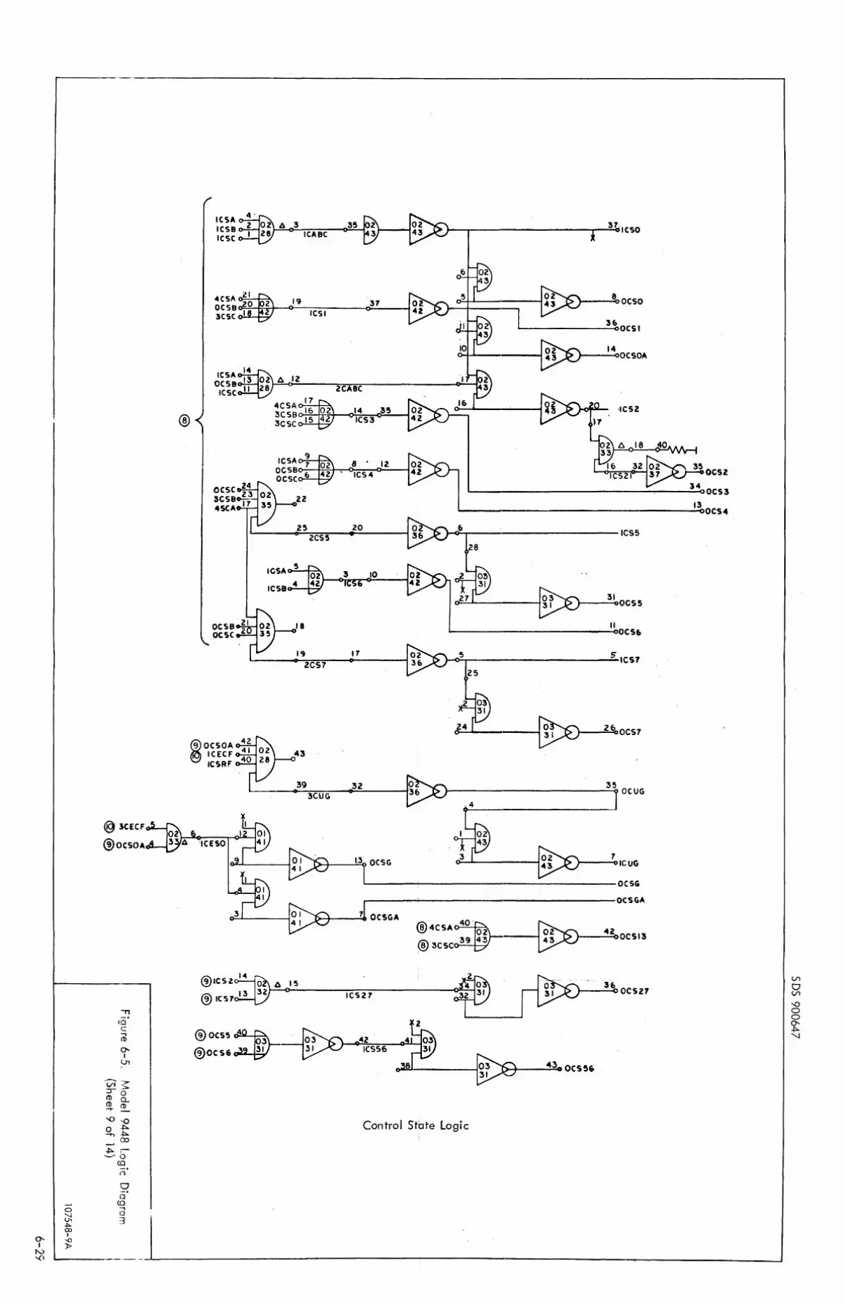
0-I
N -.()
@ 3CECF
®OCSOA
" (0' e ., ro 0-I
U1
V1~ :Jo CD a... CD m ~ -X) '-0 o p.. ~ ,~
co ..f:>., -0
~. ()
o Q'
o (Q '1 ., <..n 0 t, 3 I
-.0 »
®-<
1(5A ICSB lese
OCSBJOZ 4C5Ab 3ese 18
leSA -- --
oeSB-Icsc;iLp!.v
3 35 ICABC
19 037
0 ICSI
zeABe
4CSA~ 3CSB~~_35 3CSC-I5 l ICS3
leSA oeSB~ 0
8 • 12 ocsc-{;«' ICS~
25 20 2CS5 •
IC5A - 5
®OCSOA ~ ICECF
ICSRF
IC5Bo~ I :;'
18
19
ZCS7
39 3CUG
11 D
32
~o511~ ~ ,800CSO 43
36 oesl
~ ~3 OCSOA
~6 36 ~2e
less
I ~ -- It ,r./
~ 31 00C55 31
II ooe56
fit&os 36 I 5 1C51
25
~ 2&00CS7 6" . , 31
35 J oeUG
r-------~------------·-----------------OC5GA
6"'l 7~ OCSGA 40' ~ ®4CSA~2 02 ~200CS13 39 43 43
@3CSC
91CSZ 0 6 15 2 ® ~ @K57 13 32" 0 IC521 ~ __ 3_60 OCS Z 7
@OCSS cPV I >
®OCS6C7'< 1-,'
,~2
1C556
Z ---'
.30oeSSi I)~..l..t---
Control Stbte Logic
VI
o VI
X) o o ~ '-J

~ I
W o
o "'-.I U1 ~ ex> • o CJ
\'!I 02 J=I""cr '''Hil il F" I tg\OC~5~4 @ICUF' 31
@tWGOI
@OCERF
e OW9
8oWIO
@OCIZM @OSELS
(J !STAT
@OC'SOA_29
@OCSA
(DZWCPI
@3UIJ
@IW,MO @ qGOI
OCECO
.i7)OHROO~8 <ZI. 1 H ROI -~ :c7)IHROZ \!T OHRO!
@OCS4 @OIHGD
<D 2wePI L
@OW9 f4l~ OW" ~CSO
~OCS'_37
2 OWSB ICEeF
OFMS2
leleF
OETFS
ocn,
Icn,
,CFMF l.-lJ.OCfM' N I I )"r"r o 02 @ IW5
@t.:.\ IW6 c'Y Il;'f} 0. 7 ~ICS7 0" I
~ CO C .., CD ~ 1 til
Vl~ ::rO CD 0... CD CD -t- _
-~ O~ o ~ -.00
- r-~O -CO
o o a"
co a 3
OFMCG
@ORGER
02-32
4}ZSTRT' ~I
~ ISfLS 9SELS
~ 03-<43-37 OSHi
CECF, CETF, CFMF Flip-Flop Logic
27
tCFM'
Vl o Vl
~ o o ~ ~ 'J

0-I
W
o ~ ~ (XI I -' ...... rn
2STIH~02\ 'A -'2 8 oe ,Z-4Q2 ~
Z8 ~
I~~~I
@IWII
@oCSl3
®O(SI3
@OCS7
@OC.UH "
AI
-022
16
2
3 21
OSCI2
OU,'S
OCUS7
02-36
02-36
12
21
2
(i)4WCPI T!)OCS1
,. ...
(!):>FC ~13 ..eb • , ~~S'J--~~r--~!4~.--------------------------
@ICI2 nI OC.13 ~@OC14
."
CO c 0;
~@ISEl5
IQ2 2STRT
6
.§)OCS2~ @ICUFF: 3 ~ 03 OC'2S
(U4WCP'o1' @IC~._I
22 0(12"
RC.ZN 21
16 le.2N
RCUFr
b ~ 08 XU,,
OCUS1
03~CERF
"b 1 036
4CERF OCSIG
__ .0.43 OCSR F
-..l!'CSAF
-=
0-I
!Jt ------------------------------------------------------------------------OCI5G lil~ TO CD a... CD (1) ..... ----0 -..j::=.. o ..j::=.. ~OO
- r-~O -CO
n
9. Q
<.0 a 3
CERF, CUFF, CSRF, C1 1 2M Flip-Flop Logic
(,J')
o (,J')
--0 o o ~ "

0" I
W
'" I
o '.J lJ1 ~ ex> I
tv »
~ lUI
@ leU
@ 1C13--..J
e leZI
G oen
~ IC23---I
@oezi
~oezz 4
Glen
Soen
....A. I • ,
8 0<1
701': (i9. , ,
" co c ..., CD
0' I
~
v;-~ ::J"o CD Q.. CD CD -to
",'f;. o .j:::... -I") 00
-r .j:::...o -(0
o
o o· (0
a 3
olOe
LLT I
03 36
LLTZ
03 36
LLT3
03
-tL' ~ ENABLE
I le!l!
6>OW9
49SELS
IIL~i
31_ ~ -E- 'LLTO ill OtZI' '"""'- y V<o" 1 WeI I _'!.·Y._ ( ..... 9LUr. 03-42 \:1
eaezz
38~... 0 5 P L:J Iz.1 016 <+-
03-43 03-43
.~ <E-9LLT. 3CZIZ +-9LLT1 03-42 03"""Z
~ ~ OGOAZ 17 4-03-42 . 03-~3
~~ 9LU2 1 +9STOP 03-42 03-42
®OCS6 01HR05
24 --oi.L-< ~ + 03-43
~ ~ 9LLH leNTL I I~ ,'·0, _9v~_ <+'''lWM 03-42 ~OTEST REWM
" lel2 03 Oel6 3 37
~~ OGOOI 6 ~ 03-43 03-43
ltv-''' it,
03-42 OTt 2~ T 1 ZS I 03-4Z 33
~~ 03 03-43 31
IZ. ~<E- 9LLT4 ~ II'N 31~~8T12'S ~ fO
131 LL 1:520 I o~ (... l? 03 43 .. , ;1;/
i \r.~.J
8_ _ •. n --1Z9/6~ - ",;,:,,'0 U-j I H.. f~or-ntu < +-KIIT ~r \L'"
~) o .. J
•• on : : 'J "2 r rj UTRT
'EOTS-+ ) 011 u 9"
-i> ) 0'"
ZCNTl
9RDYS:: jt"z r~ r:j r10RPnu TO""'Z-O~
03-43-05
~/ .,.I
9AANS~-) 019 _ Q ail' ~
-+ >--03-43
OGD"4
Tape Station Signal Logic
SIZT 03 n
"'til 01 <+-03-43
COM.
OTFPS
o lOTS
OEOT5
~ cfl.
~t.s ~I~: ,;'" cd ~ 1'\& j},.ft
u·
"",ANI I::ZbO (pPI
t.,c
VI o VI
-.0 o o ~ 'l

SDS 900647
G ICIS (i)OAANS
DI~ ICI6 ~ 6 OCl3 '-"' ~ 080TS
OCI5G --.------------O:'~H
REMOVED WHEN INSTALLED
(i'lOAANS ~OCI6
G> 1C13 31 ~ICIZ
OROYT
0"0''''
Skip Logic
Figure 6-5. Model 9448 Logic Diagram (Sheet 13 of 14)
107548-13B
6-33/6-34
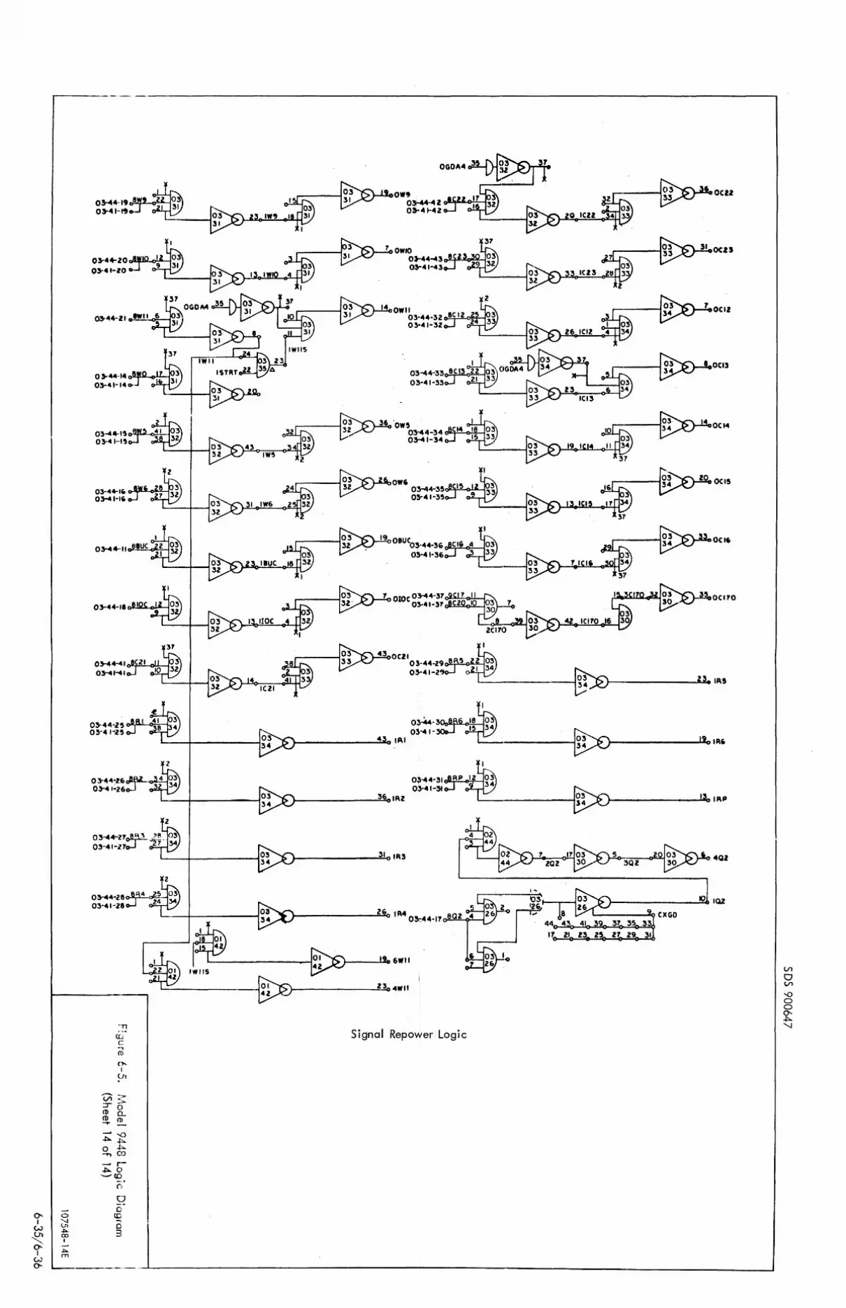
0-I
W
~ 0-I
W ~
o 'J lTo ~ 00 I
~ m
03-4 ..... ' oRf~" o!;!;I, 03-'''-41
0~44-Z5 ovp I 0:::' h 03-4 '''25
Ol-44-16cPP" 0:"" I 0"""'·26
03--44.280 51, ..... ~:'
03-"1-28
on ill C --.; CD
()o. I
ell
- -".. (.Il 00(;:.. :Jo (1) 0.. ro ('I) ..... ----0 ~+:... o +:... -t-o co - r ~o -co
n
o o
co -. o 3
o.o •• ~
ow. ~ OH~~Z. 11 03-~"'~2 I 32
O"~~~3 8 03 OWIO ~' Ot"" 1-43. 9 32 .
OW" 03-""-32 o"j -.. 0:; ~ 03-411-32
OCI3
~ OW6 03-44-35 15 :5 0)-" 1-35 3 3
0'"""-31 :5 """"'0 7_ OIOC 03-" 1-31 30 ~" 7 oel10
2el10
"3_
0C21 2~5 1043 ~ n.IRS 0~-4"- I :3 03 0~41-Z 34
03~_~8103 134 ~ 03-41- 03 "c IAi \-. ______ '' .... 311000 �RI -------34
0~-44-310"i'r D:..r I 0~41-31
'b3--- - I~ IRP .------I~~ PJ h..IR2
L ____________ ~~loIA3 1
5 ___ ~ ~4QZ
SQ2
230 "WII --.----~-
Signal Repower Logic
Vl o Vl
'-0 o o ~ "'-...I

CHASSIS 00
44 45 4' 41
SDS 900647
26 17 28 29 ~o !al 32 33 34 !.~ 3" 31 38 39 40 41 42 4 ~ 44 4~
_2
I
Model 9446 Module. Chassis Power Distribution
2.& l1 l8 }Q 30 31 32 !! 34 ~!> !B· 3' ~A ~g .. 0 41 42 4!1i 44 4g
CHASSIS
01
44 -45 ~
46 H - ~
02
03
Model 9448 Module Chassis Power Distribution
TB4 I +50Y
-! ov :. :3 +aY :2 -25
+1'
ov +8V -Z5V +25V
Figure 6-6. Module Chassis Power Distribution (Models 9446 and 9488)
107549-10E
107548-19
6-37/6-38

DESIGNATION
LOCATION
KEY '-
P80
6-21
SDS 900647
245 244 243
242 241 240
...-_--=2.:::,3.:.,9 oO-----e 238 237 236 235 99
+Z5V 0 47 47 0 ~-:-7 .......... -t--t-t-_-+ _________ -+-______ --:!9~8~ -zsv 0 46 46 0 ~:~5_~;-+-_ _t----------~--______ --~9~6~
.t-8V 45 4SJOO _ 93 94 0
OV044 ~4 I 92 ((23) 0 43 ~=-0<>_-___ --2-3-4-+--..L-91-9-1 _____ -+-______ ....!:14~2:_o (e22) 0 42 0420 1 E>o-:8;.:;.9<1-------+-----------~-___r-----.!.:14!!1~ (Cl~)~~~~3- 232 9 189 233 0190 140_
«(20) 0 40 . ~-o-§:...;.7-"<>------t-----------+---r-------!.::13:!..:9~ (CI9) ~ 23 ~~-;6<>_ ______ 23_0_t---~ql.;..8-7-------.;2:::..:3;.;.1-I+-----...: OI.::8.::8 __ ___!.::13~8~ ~I~~ ~::.::::5<>------_t-------------+---r-------~13~7~ ~ L22 ~
(m) 37 37 .~ 84 228 9 185 229 \,I 186 136
(CI~~ l~2~~3<>_-----~_+------------~--~----~13~5~-(CI5)~ ~~2<>_-------22-6_t----..L-918-3--------2~2~7~--~018~4~---~13~4~-(C 14) ~ o-§,,.:.I_o_ _____ -:-:--:-+ ___ -:-_____ -+ __ _r_---.-!.::13:!.:::3~-
(CI3)~ ~;~0<>_------22-4_t---..L-91-8-!--~-2-2-5~---OI-8-2----~13~2~ (C12) ~ ~,.::..9-"o_---:--:+---------~----.--__ ---!1~3l-I-o (~P)~ _~7~8-o--------2-22-+-I __ -..L-91-79-' ____ 2~2~3~1+_--~01~80~--~13~0~-(~6)~ ~~7o_----:__:~---~-----~-~_----~1~29~ (R5)~ ~~6o-----2-2-0~~r----9~1-7-~------2~2~1~--~017~8~--~1£28~-(R~~ ~,~5_o_-' ______ _t-----.;------+---r----~12~7~ (R3) 0 27 0 27 00 .... -:;7;-:;4_o_-----2-18_t--..L-91-75-· ____ 2_19-+ ___ 0_1_7.:..6 __ ~12~6~-(R2)~ Llo~,_3<>_~------t----------~----,_---------~12~5~-(RI) 25 25 ~ 72 216 9 173 217 ~ 0174 124 (WI~~ Rfu ~~~ ______ .t-_____________________ +-______ ~ ______ ~12~3Lo-(wI3) 0 23 0 23 0 ~9-o~ _______ 2_14_t __ ...I9~17...:.1 ______ .=.2.:..:15=-+ ___ 6::..:..:17-=2 __ ~12f!2~ (WI2) 0 22 0 22 0 L9 ~20~------t-----------+---.-----...!I-'Lo21 (WII)g21 ~!!o 212 9 169 2131 6170 120_ C WIO) 20 ~ t~9 ~;..:.7: __ -_ -_ -_ -_ -.:-_ -_ -""':" -__ +t -_-.... -___ ....J_ '-_-_-_-.:-_-_ -_-_ -_-_ -_ -_ -_ -_ +-1--_ -_ -_ -_ -..., -_ -_.:.._ -_ -_ -_ -_ -_ .!;.lI~lgt: (w9) 0 19 ol9...0 0--2.2.0 21'0 9 167 2110168 1111-0
(1 0(,) ~o--_6=5<>_~---:_::_~---___ ---------~-----r---~_-L1 UI7~-
(02) g 17 17 -Ji4_ 208 9 165 209 0166 (Wb) 16 ~ , ;§:-:;;~<I::::::::::r::::~::::::::::::::t::::::::::::::j:i:I~~ (W~)~ L2 ~~2Q_~----20-6_+-~..L-~1-63------2~0~7~-----0~1~6~4---~1~14Lo (wO) ~;;.;.IQ_ - ____ :-:--t---?:R2~8_::_------+----,--_---L1 ~13~ ~ 13 13~' 60 204 !Vv-r-y 161 205 0162 112 _
(r.Ats' 12 12 C~4 59 R31 III
(au()~'~~VV-o-~50~ _______ 2_0_2~~~9~15.:..9 ________ ~2~03~_A~A~A~~~16~0~ __ ~1~10~ (~IO 10 'RI. 57 P27 .I".() 109
~ 9 9 'tR3 56 200 AyAVV .157 201 yAVV ~ 158
~ 0 8 0 8 'tR2 .. 1 ()-";~'Q_ .... ------_t-_..L------:..:...~....:...:...:...--.-:=--~10L!::8~ crew . 55 R2"l 107 _ 7 7 CRI 54 198 0 155 199 A .,,:"v 1 156 ~ 0 6 0 6 c o;~: 1 - :~~ (~ ~5~ __ ~_~5~ ____ ~5~2~;_r-______ 1.:..9~6~ ____ 9~15=3 ______ ~1~97~~ __ ~-6~15~4~ __ -1IQ04i-o
(~O 4 0 4 0 0 51 103
(@> 0 3 0 3 0 c 50 194 9 151 195 0 152 102
I...~ 0 2 0 2 0 0 49 101 ~ 0 I 0 I 0 0 ~ 192 Y 149 193 0 150 100 0
Figure 6-S. Cable Plug Module PSO Schematic Diagram
PSI
l07548-15A
6-41

6-42
DESIGNATION pel
LOCATION 03J44 KEY
+Z5V -2SV +ev
0 47
0 46
6-32
470
46 0 45 0
97 95 93 0 45
44 44 :. 91 Ov
8C2~
8(22
I eC2 800
8(19 8(18
9(17 8CI6
8CI5 8(14
8CI~
eelz 8&1P 8~6
8R5 8R4-
8R! 8RZ
801 eWI4
8WI3
8wIZ
aW11 SWIO
ew9 SICC
SQ2 8w~
aW5 BwO
7wes E,M1G
aBuc. 7510
1WHS 1ECM
72WP
HW6
1ZW5 1ZW4
7l.w'3 7l.WZ
llWI
43 43 90 42 42 69
41 41 88 40 40 _ 87
~ 86
~ 85
0 37 36
037
0 36 ~ _ 83
35 35 82 34 34 81~
~
33 33 60_ 32 32 79
31 31 78 30 30 77
'" 29 29 76 28 28 75
27 _27 _ 74
26 _26 73
0 25 025
0 ~.1.J." 24 24 71
23 _23 70 22 22 69
21 21 68 20 20 67
19 _ 19 66 18 18 65
17 17 64 16 16 63,
15 15 62, 14 14 61
13 13 ~ 60 12 12 R'~.~' 59 II II 't~ 58 10 10--.~ 57
9 9 L~4 56' 8 8 :P3 :~~ 55
7 7 ~ _54~ 6 6 53
5 5 _ 52_
4 4 51 -3 3 50 2 2 49
0 1 01
0 ~
SDS 900647
245 244 243 242 241 240
239 238 237 236 235 09
234 9 191
232 9 189 233
230 9 187 231
228 9 185 229
226 9183 227
224 9 181 225
222 9 179 223 c
220 9 177 221
218 ?175 219
216 'i' 173 217
214 9 171 215
212 9 169 213
210 ? 167 211
208 9 165 209
206 9 163 207 c
204 9 161 205 )
202 9 159 203
200 9 157 201 I
198 9 155 199
196 c 9 153 197
194 9 151 195
192 ( ~ 149 193 c
Figure 6-9. Cable Plug Module P81 Schematic Diagram
98 _
96 94"" 92 --
"V
142 141 "V
0190 -v'
140 139-
0188 "V
138 137 -
0186 ....
136 _ 135
0184 ~
134 1.33-
0182 -132 _ 131
0'180 ~
130 129 -
6178 ....
128 127~
0176 -126 _ 125:
0174 124 123 --
0172 -122 121 ...... > peo
0170 120 0 ' 112 0
6 168 118 117~
0166 -116 115~
0164 114 113~
0162 112 III
0160 110 109 _
0158 ~
108 107~
0156 ~
106 105 ~
o 154 ~
104 103 ....
o 152 102 101
0150 ......
1000
l07548-16A

DESIGNATION LOCATION 03J4Z KEY 6,3& I
+Z5V -Z5V
+ev ov
9TFPS 9RDYS
9EOT5 9aOTS
9RDAS 8ROAS
9SELS 9AANS
9TEST
9RTRN
9RTRN 9RTRN
9LLT7 9LLT6
9lLT5 9LLT4
9LLT3 9Ll.T2
9LlTI 9Ll.TO
9WDAS
eWOAS
(9LLT 7) (9Ll T6)
(9lLT5) (9LL T4)
(9LLn) (9LL T z)
(9LLT' ) (9LLTO)
(8SI2T) (8- 12'»
C'!lHlP) (eREWM)
8WRTS
8REWM
9ST6p 8TI25
8512T
047 47 " 0-1.7
046 46 0 0-2,5
045 45 0 93
0 44. 440 0-2 1
o 43 0430 0-1.0
~9_
041 0 41
0 ~ 04Q ~ oJ!~
039 ~ ~6
038 ~ c>-§~ 37 37 84
036 oM-o ~3-
035 ~ ~2_
034 0 34
0 ~I
033 0
33 0 ~O 32 32 79 -
~ -0
31 0 31 0 0.28
30 30 77
029 0 29
0 0-26
028 0 28
0 0-1:5
027 0
27 0 o 74 o ,§ 0 26 0 on
0 25 0 250 cr1?-
024 0 24 0 0-11
23 .... 23 7()
022 0S:20 ~9-
o 2 I 0 21 0 0-&-8 o 20 0 20 0 0 67
~ 19 19 66 ~ LI5~)
8 :~ 17 ~.
0-£-4 ~3
0 15 ~ 6'~ ~
0 14 oli-o 0-2,11
o 13 0 13 0 o-M-~ ~C}~
~ 02-8~
~ 021 ~ 02.!t. o--L---o-Lo 02) -~ ~~ o 6 0 6 0 Rl - 53
~~ o 4 C! 4 0 LI 0.2.'-
8~ ~ ~ : 50
~ n,1 I 411 -
SDS 900647
245 244 243
: 241 242 > 240 ~
239 l 238 1 237 236 .......
l 235 I p9 --
234 9 191
232 9 189 233 bl90
230 1 9 1.87 231 bl88
228 9 185 229 bl86
226 9 183 227 bl84
224 9 181 225 &182
222 9 179 223 6180
220 9 177 221 0178
218 r--<i 175 219 bl76
216 r-c? 173 217 ~'74
214 HI71 215 ~172
212 ~ 169 213 ~170
210 9 167 211 r- ~168
208 r?165 209 6166
206 ~ 163 207 .:::0"164
204 """hl.61 2J)5 , ~162
202 ~159 203 LO 160
200 r--c? 157 201 L-.J"158
198 r? 155 199 ,....--6156
196 9 153 197 r..6 154
194 L....c? 151 195 ~152
192 ~149 193 1........4150
Figure 6-10. Cable Plug Module P83 Schematic Diagram
98 96 94 92 _
142 141
140 _
139 138 _
137
136 135
~ 133
0
132 131 130 _
Pl4 129
128 _
127 0
1260
125
124 123 _
122 121 ....
1200 ,,90
118 --0
117 0
II§ 0 115
114 0 113
1'12 III 0
110 109
1080
107
106 _ 105 _
104 103
102 _ 101
100
l07549-9A
6-43

6-44
+Z5 +8
-Z5
o 9TFP
9RDY
9EeT 9aelT
DESIGNATION
LOCATION
KEY
v 0 47 V 0 46·
v0 45 V 44
50 4~ 50 42
5 41
S 40
39
S
S
8RDA
9SEL 9AANS
38
37 ~6
35
PU
00-26 6.38
47 0 97
4§ 0 95 45 0 93 44 91 .
0 43 0 090 0-
~ o 890-41 88 40 87
39._ 86 .38 85 - ~
37 8~
36 83
35 82 ~~81
33 33 ~
9TEST
7S[LS
9RTRN
9RTRN 9RTHN
9LLTT 9LLT&
9LLT5 9LLT4
9LLT~
9LLTZ
9LLTI 9LLTO
9WDAS 8wDA5
6H2 SEOT2
oaTUZ SBOT2
O~-WAI
ORWPI
ORWA2 ORWP2
nrl SEOTI
oaTUI
SBOTI
SWRTS
SRF.WM
9~TelP ,T125
•• 11T
3z 31 ~O
29 28
0-.27 26
25 24
23 22
21 20
19 18
17 16
15 14
13 tZ
II 10
9 8
7 6
5 4
g-i -I
80 -32 RI 79 -
31 78 -30 77
_29 .... 76 _28 _ .... 75
27 74 26 73 - -25 72 ;Z4 71
23 70 22 69
21 68 20 67
19 66 18 65
17 64 16 63_
J5 62 ~ 14 ... CR2 61/
13 .. ,cR3.. 60 12 :CR4 59!
.... II .. CR5. 58 10 ::eRG 571
9 56 8 55
7 54 :t 6 ,~CR7 53:/
r"I
5 52 4 51
- 3 50 2 49 .-I 48.
SDS 900647
245 244 243 242 241 240 239 238 237 236 235 99
234 9 191
232 9 189 233 6190
230 1f'187 231 6188
228 r? IS!) 229 6186 l' CRI
226 Y 183 227 6184
224 i...c? 181 225 0182
222 If' 179 223 6180
220 Ii 177 221 0178
218 ? 175 219 6176
216 Ii 173 217 6174
214 .1f'171 215 6172
212 If' 169 213 6170
210 9 167 211 6168 C3
208 .Jl -'" 165 209 6166 C2
206 V ~163 207 6164 'hcRB
204 W 1f'161 205 6 162
202 1f'159 203 . r--6 160 C4
200 1 157 C1 201 6158
198 V ~155 199 6156 ,*CR9
196 ~. yl53 197 6 154
194 1 If' 151 195 Yl52
192· 1f'149 193 0150
Figure 6-11. Cable Plug Module P84 Schematic Diagram
98 _
96 94 92 ~
142 141~ --140 .... 139 --138 137~ -136 135 _
134 _ 133
~
132 - 6& 131
~
130 _ 129 -
...... 128 127 _
126 125 -
124 123 :
~
122 0
121 ~
120 '119
~
118 117 -116
"15 ®
~® 113
~
112 III ~~ 110 109-- ® 108
-..J07--@
I~@ 105~
I 104 103 --
102 _ 101~
~
100 --
P8l
@ INDICATES NO CABLE CONNECTION AT THIS POINT.
l07549-8B

SDS 900647
POLARIZING PINS: 20 &. 2<4
.... SV ~~
GROUND ~~
27
26
25
+25V~--r----T----·------------~----------------------~--__ +8V
R2 R3
CRI TO E ... --....,.----.... ----1
CR3
CR .. . RS ':"
R9 RIO
CR8 -2~V
~ CA6 CR7
- 2~V TO A
412 -40 CIRCUIT I -41 .. 3 39 1&36 38 37
I 2 341 3~ 33
I 32 31
.... ~ 3 29 30 28 2-4 23 :;:) Q. W '" 21 22 20 19 18 ~ !< 0 10 16 1-4 13 12 j I.!) 6 9 II 10 7 8
~ w CIRCUIT 7 .. 6 0 1&.36 2 3 ~
!!! III < ./l Z ..... 0 0 C/) 'II ..... 0 :::> a: :::> w
~ ~ Q. :::> Q. ........ Z ..... ..... 0(::::1
W W - w :::> ZQ.
!< .... a: 0 - ..... < ~::::I C) C) ..... ....
~o ::::I U Q. W .... t- a: ::::I 0 0
1028518
Figure 6-12. Cable Driver AX14 Schematic Diagram
6-45/6-46

POLARIZIN' ,.NS: I' &. 30 +25V~~------~
+25Y 47 0 R21 R22
-25V "'0 +IV 4'~
"2 aROUND 44
CRe CRt CRIO CRII
45
41 6 6 39
2 4 5 . 'I 6 1 8 9 10
g] 31 +ev
35 RI
sa 3.
2.
21
25
23
oj R6 CR'I
+ lCi 2. i'Z5V
17 Re C4
+ev VRI
C6 e7 ce C9
RIO RII I -25V 1 -25V
24 32 30 28 20 13 18 /4 /g /2 . 22
• ..0 u " tJ ~ .,. .&. --. Z Z
D. D. ~ !: z Z Q. ... a: A:
Z Z z ! z a: a: a: Q. ii:
\ If I • m m
SI E3
HRI R26 CI3
II R2l
~ +25V
R2 R"
RS
CR2
CRS
C2
--Q2
Rt7 Rte RI9 R20
~ II 26 17 3
£ c Go ... :!)
z z ~ Q.
Ci: 0:: ... L, ::l 0
m
SDS 900647
NOTESi , r;a. THE TAILE IElOW USTS P'N CONNECTIONS TO IE MADE
DEPENDING UPON THE FREQUENCY OF THE CRYSTAL USED.
CRYSTAL fREQUENCY
PIN COHN'ECTIONS
RANGE b c d , CJ h I J 1 m ft p
I MC )( " X TO
)( )( 300 KC
300 KC X X TO X X
100 KC X X
100 KC )( X
TO X X 30 KC X X
)( )(
30 KC X )( TO
10 KC X )(
~ X )(
m OVEN ASSEMBLY IS OMITTED ON C)(13.
~ IF" O~TPUT PIN *10 IS USED AS CLOCK ,F"OR F"lIP-FLOPS" PIN 9 SHOULD BE GROUNDED NEAR THE FLIP FLOPS; OTHERWISE IT MAY BE GROUNDED LOCALLY.
@) OVEN COYER SHIELD IS SAM! AS GROUND FOR eX14.
Figure 6-13. Crystal Clock Generator CX13 Schematic Diagram
1021690
6-47

..,.. A ~ il ~ -- 7 I -' V 1'...1,,-,.; ,""e
+2&Y~--~------------------------~--~~-----------------------T----?---------------------------~ RI R3 + V R5
+uv "'~JW
Gfa CR4 VR2
CR~ RS CI CR6 GRl G2 ,R,tO CRI
GR9 GRIO
.. Al2 CRB CRIS CRI7 CRI9 RI4 CR20 GR21 CRZ
-25V RI5 -25'~ -25Y -25V
...., ()'
ICIRGUIT I 2 33 34~
\:), 35 I 3937 3 <41 42 " 1
z 2 2<4 Z529 26 I~ 28 27 3 31 32 II 3 2 13 ~ 21 15 I~ 18 16 3 22 23 II
CIRCUIT 4 2 6 <4 9 5 8 1 3 10 12 II ~ "'i'
z z z z z z cL~ ~lII z z z z - - - - - i::) :::) ~ - - - -,.IGNAL ... ~ ~ ~ ~ ~ q: 0 0 q: ~ ~ ... ...
W 1&1 1&1 l&.I ~ t;j t;j.5 1&1 "" l&.I "" NAME 0 CD II) II) II) en en en II) II) 0 "" l&J W W
)( -' ~ cJ t \I) ~,~ a: a: a: a::: z 0 Z ci 0 ::) vt a::: \U .<.3 )( ::I ~ lU Vl z
~ z d ::J
~ 0 ::I (Jc i <0( W 0 1-. ::E 0 en 2 p ~ Z ~ U
~ ':l (;, 0 0 ~ ; 0 () :::E u
0 0
~ u
14~/L'-}E>·t /ZIF6,S- r t l., \ J _~ 112.':0. $ f.E.<..1 11'- FOJ2.. ., ~"
6-48
SDS 900647
POLAR IZING PINS: I & 30
RII + 25V 47
RI9
-2'V 460 R20
R21 +IV 45
GROUND 44
36
17
+25Y
Rlf
43 '38 30
... ,.eV
A VR3· G3
I
+tY
GR29 C4
20 19
Figure 6-14. Counter FI ip-Flop FH 15 Schematic Diagram
101002B

SDS 900647
POLARIZING PINS: 16 , <40
+ 2SV <470
-2SV 460
+2SV~--~--~~-----~------------------------------------------------~--~
+8V~~~--------~
R4 RI R2 R3 R5 R6 CRI
CR2
CR3 CR4
CR7 CRa CR9 CRIO CRLl
-25V -25V
TO A
CIRCUIT I 39 40 42 43 37 38 41
I 2 32 33 3~ 36 30 31 34 3 25 26 28 29 23 24 27 4 18 19 21 22 16 17 20 5 " 12 14 15 9 10 13
CIRCUIT 6 4 ~ 7 a 2 3 6
~ ~ ~ I-- I-- I-- Z ~ ::::I ::::I W -I-- Z I-- 0 0 on I-- I--
SIGNAL w 0 w w w w NAME CJ) ~ CJ) I-- I-- 0: on CJ)
w :ll w w W Q: 0 Q: CJ) \I) z
~
u w 0 u W I- 0: ~ w W I- U ~ Q:
I-..t; W 0 0 a: « I.!)
0 u I.!)
103131B
Figure 6-15. DC FI ip-Flop FH 19 Schematic Diagram
6-49
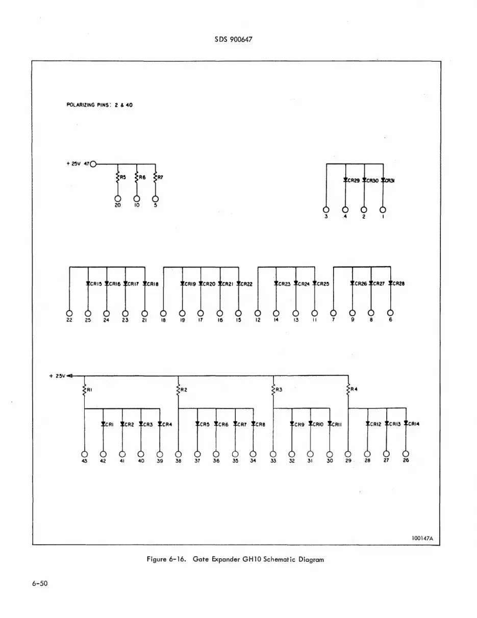
SDS 900647
POLARIZING PINS: 2 & 40
+ 25V 41
:3 .4 2
22 25 24 23 21 18 19 11 16 I~ 12 14 13 II 9 8 6
+ 2~V~--~----------------------~----------------------~-----------------'
RI R2 R3
CR6 R1 RII
42 41 40 39 38 31 34 32 .31 30 29 28 21 26
lO0147A
Figure 6-16. Gate Expander GH 1 0 Schematic Diagram
6-50
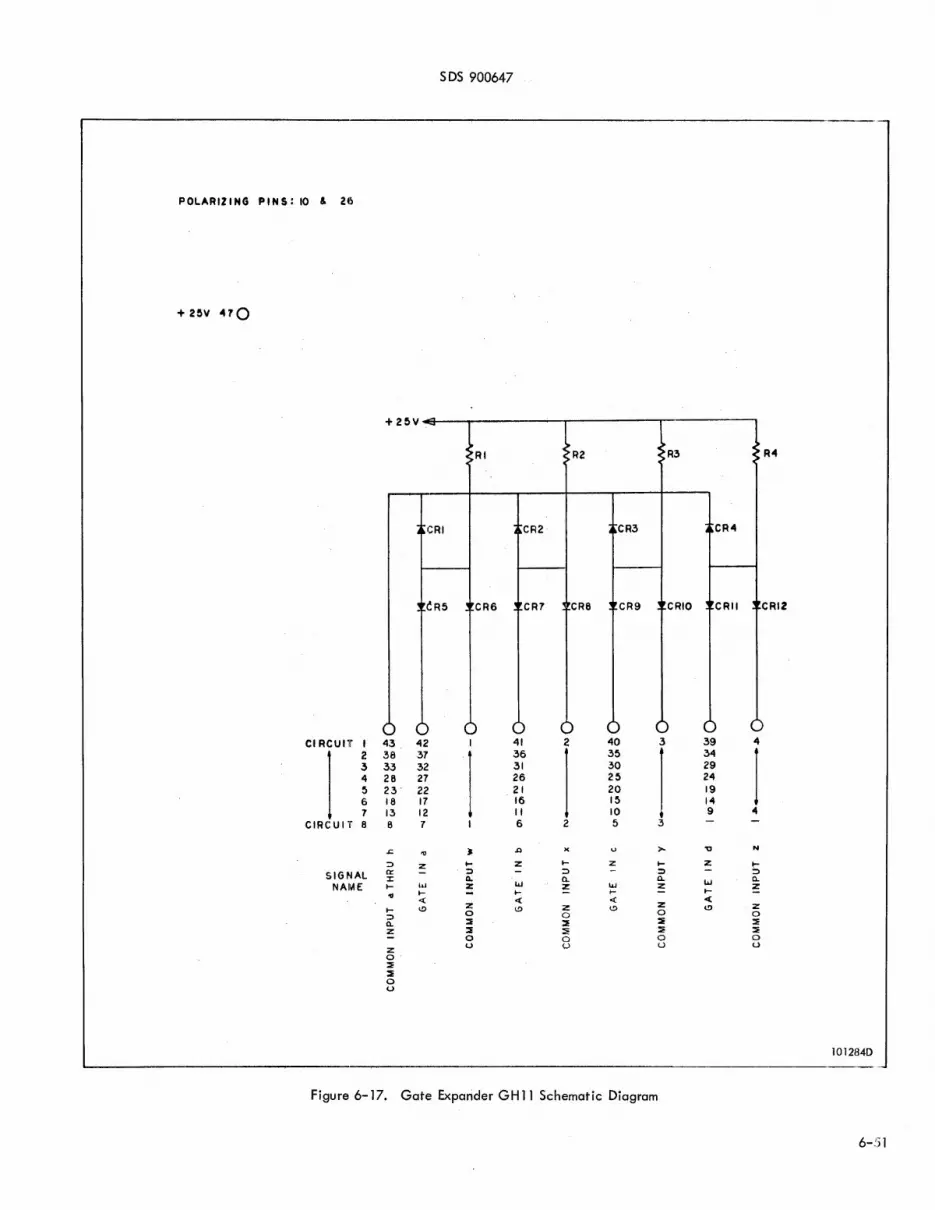
SDS 900647
POLARIZING PINS: 10 & 26
+ 2&V ~10
+2&V~----~----------~----------~-----------'
RI R2 R3 R~
GRI CR2 CR~
~R5 CR6 CR1 CRS CR9 CRIO CRII CRI2
CI RCUlf I 43 42 41 2 40 '3 39 <4
2 38 37 36 35 34
I '3 33 32 31 30 29 4 28 27 26 25 24 5 23' 22 21 20 19 6 18 17 16 15 14 7 13 12 " 10 9 4
CIRCUIT 8 8 7 6 2 5 '3
.&:. 'IJ ~ Jl )( >- 'C N
:> z .... z .... z .... z .... SIGNAL a:: :> :> :::t :::t
:x: Q, n. a.. n. NAME .... w 2i: w
~ w z w ~
11 .... .... I- .... « « « «
l- I,!) 2i: I,!) z I,!) z I,!) Z
:::t 0 0 0 0 a.. :2 :::I! ::i 2
~ :2 ~ ::i ::t 0 0 0 0
Z U U U U
0 2 2 0 u
101284D
Figure 6-17. Gate Expander GH 11 Schematic Diagram
6-51

SDS 900647
l04299A
Figure 6-18. Gate Expander GH 14 Schematic Diagram
6-52
'" I tn
~ '" I U1 ~
"T1 cO· e .., m
'" I
:.0
o o· 0.. CD
(;) o -to CD
Z ?
(;) 7\ tn
VI o ~ CD 3 S-o o c·
co a 3
a a
'" -I>--I>-CtI
+ 25V
+25V
+25V
"tiRS
2
R6-
22 ~ 2<4 23 17 21 20 19
RI R2
41 43 42 38 40 39
POLARIZING PINS: 2 , 22
R32 ~:fCR35~CR.'36 VI 0 VI
-0 0 0 0-~
18 14 16 15 13 12 II 10 9 8 6 5 4 .3 "
R3 R4 R5
34 37 36 35 31 33 32 26 30 29 28 Z7

+25\1
+ 8\1
GRD.44
43
-25V
40 IN
RI
4' 37
1&
3
+25Y
CR2
R5I
VR5
VR6
VR7
VRIO +
VR9
VR8
R!l2
+ + C II CI2
CI3 +
R54
CI4
------....... -~+12V
Q2 C!.-FI _pC4 b R4 Q C
+ R6
R5 R7
-6v
+12V
-a5V
AI (50S 302)
2
RII
-6V
+25V
POLARIZING PINS 3 &. 37
+25V
C5
, -25V
R48
AI3
+25V
RI6
+1 RI1 IC1
":' RI9
10 TPI
-25V
9 Tlt2
~50
13 TP3
18 TP4
+18\1
CR5 CR4
14 TP5
1 l
6 12
RE~D
DISABLE
SDS 900647
+25V
-25V
Q9
6 OUT
Figure 6-20. Data Ampl ifier HX29 Schematic Diagram
107385-1C
6-55/6-56

505900647
~----------.----------------------.--------------------------------------------------------------------
+ 25V ~7 POLARIZING PINS: 3 , 39
-25V ~6
+ 8Y "5 TO A
GROUND' 44 YR3
VR" (I All
VR5 -25V
+ 25Y C B
+25V
CRI RI R2 TO B Ril
Q2 C R2 C R3 VR6
VR7 CZ
R5 R8 VRS
':'
-25V ":' ":'
TO C
VR2 RIO
":'
AI5
':'
CIRCUIT NO'S.
34 36 38 32
22 24 2 26 20 42
12 14 3 16 10 OUTPUT
4 6 .. 8 2
TEST SELECT POINT AEAD SIGNAL
1
107365-1A
Figure 6-21. Gated Read Ampl ifier HX30 Schematic Diagram
6-57

0-I
01 CO
"T1 cO' e ""I CIl
0-I ....., ~
G) c CD 0...
~ CD
~ "'0
~ CIl ""I
:::r:: X w
Vl o :::r CIl 3 a o· o o·
(C
a 3
0 ~ '" ';'J tD
+25V
RI
CR3
CIRCUIT I 10
2 10
3 10
~ 10
DATA
i= ~I
R3<
-25V
R5
~CR~ CR5~
40 42 39
25 32 26
16 20 13
.. 6 2
POLARIZING PINS: 3 , ~I
f R2
~2 +25V ~7 0
VR2 CR2 -25V 46 0
r4 +8V 45 0
-25V GROUND 44 0
Vl
R6< 0 Vl
-0 0 0
~CR6 ~CR7 ~CR8 0-~ '-I
CR9 CRIO CRII
41 35 36 37 38 43
31 35 30 29 Z8 34
18 35 2~ 23 22 14
5 35 9 8 7 3
DATA

SDS 900647
POLAAIZING PINS~ 5 , "
+-25 V 470 +25V +8V
-25'.' -5.6v -25V 460
+8 V 450 AI2 AI4 RI9 RlO R21 R22
GRO 44
33 VA3 + C2
32
II
10 -= 9
7 -25V +5.6V
5 -= 3
8 2 + C3
+25V
-5.6 V +5.6
+BV
R8 R9 AIO RII RI
CR2
R2
CRS CR6 VRI
+- CI RS
R4
-25V
CIRCUIT I 40 22 24
2 38 26 28
3 36 12 '''' 4 34 16 18
117694-1A
Figure 6-23. Delayed Photosense Ampl ifier HX48 Schematic Diagram
6~59

SDS 900647
+~V 47 POLARIZING PINS: 2 & 44
-2~V "ISO
+8V 4~O J: GROUND 440
Tel' 43 36 21
R9
41 4 31 26 27
+2~V~---'---------------------r--------------~--------------~
ff1 II to 8 18 22 16 15 19 29 28 14 12 13
+ 8 V ...eI-------.
VRI
R2
- 2~V
CIRCUIT I 39 42 CIRCUIT 2 32 .35 CIRCUIT .3 20 6 CIRCUIT 4 17 5
~ .... 0: is
SIGNAL w 0: NAME .... w a:
w ~ ~ w
> ~
l00135A
Figure 6-24. AND/OR Inverter IH 1 0 Schematic Diagram
6-60

POLARIZING PINS 2 & 16
+ 15'11 410
-2SV 41.0
QI ~f§CI RZ
1 -zsv
" cO· e ~ 0-.
0 0 I +Z5V '" ~ CIRCUfT I 37 3G
CIRCUIT Z 35 34 <,R3 <'R4 ~R5 <'R6 ~A7 ~A8 <R9 <RIO <RII <RIZ <R13
0 CIRCUIT 3 12 13 :;::c CIRCUIT 4 10 II
G'> ; ~ C
CD SIGNAL IX: 0 Vl I&J 0 HAM! .... ~ CRI CRZ CR3
ttt ttt tt S" IX: Vl
< ~ ~ '" (& ~ 0 =+ ! 0 CD 0-. ~ ..f::>.. - " I CRIZ CRI' CRIo4 CRIS CRlo CRIT CRI8 CRI9 CRZO . CRZJ CRZZ
Vl 0 ::J CD 3 19 21 20 18 14 17 16 15 8 9 6 3 5 4 a 0
0 c· +Z5Y co ~ c 3 >A 14 ~R15 ~Rlo ~JUT ~R18 ~R19 :>RZO :>R21 <"RZZ <"RZ3 <"RZo4 <"RZ5 2'RZo ~RZ1 ~AZI
CRZ3 CRZ4 CRZS CRZEI CRZ7 CRZS
CR39 CR4Z CR43
0-. I 0 0-. 0 3943 4Z 41 40 38 28 33 32 31 :30 Z9 2& 27 Z5 24 23 2Z
~ w
1 ~ 0-.
""
'" ...q--.0 o o 0-
V'J C V'J
POLARIZING PINS; 10 & 34
+ 2~V .. 70
- 2~V "60
+ 8V <4~~
o-ICI GROUN D .....
+25\1 + 8V + 25V
RI7 Rle
CRll ICR23 RZ<4lCR25
-25V
6 5 8 II 10
+25V + 8V +2~\I
RI R3
CRI
CR5 ICRi CRl IC~8
-25V
CIAQJIT 1<41 38 43 34 32 CIROJIT 2 22 21 23 18 15
z Z I- Z Z J
SIGNAL UJ 0 DC I6A ~ NAME I- I6A IX I- I6A c: 0( I- I6A l-
\.!) IX f.!) a:: I-..., IX LL!
> UJ > z > z z
.. 8V .. 25\1
CR26iCR27
-2~V
14 17 16
+ 8V +25V
R~
CRl
CRD ICRIO .
-2~V
36 28 27 19 12 9
I- Z Z J 0
I6A a: I- I6A IX 0( I-
I6A f.!) a: l-IX I6A
> I6A z > Z
.. 8\1 + 25V
R23
CR2alCR29
-25V -25V
20 30 29
+ 8V +25V
R7
CA<4
CRII ICRI2
-25V -25V
31 25 2 2<4 13 ... I 3
I- Z Z Z :l 0
I6A I6A a:: l- I- LL!
IX 0( 0( l-LL! f.!) \.!) IX I- LL! IX Z > LL! 0 z > :::E z :I
0 u
+ 8V
-25V
33 37
.. 8V +25V
RIl
26 040 39 7
I- Z Z J 0 .. .Q
a: I6A LL! I6A l- I-I- 0( 0(
a: C) C)
LL! > z
N
I
"-Q)
-I"-Q) E ~ E
...... 0)
-t 25V
Q) 0
-00 <-' u c .... Z 0
« ~ .l:
• U . ..Q II' N
I -0
Q) ":::> 0)
u...
R26
CR21
35
+IV
-25V
042
I-:l 0
a: ..., l-IX ..., > z
£0 co M 1(')
o
M ..0
I ..0

. POLARIZING PtNS 2' 8
+25'1 47 r-...... ~
81 -25'1 460 0-.
~I +8'/ 45 D----.h Ct
GROUND 44 o----T ~3 3 2 4
RI!
VR5 AT3
·25'1
C I R CUlT ,. ,28 30 29 27 CIRCUIT 2 17 16 18 19 CIRCUIT 3 6 5 7 z
• ~ ... eE: ... w !
;:) ::J u:. 0 0 LA..
a:: a:: 0:: :l
1.&.1 LIJ UJ CD
SIGNAL LA.. LA.. l.L. NAME LA.. LA.. l.L.
::l ::J ::J CD CD /XI
+8'1 +8V
VRI VR2 ATI
-2~V - 2~V
CIRCUIT I 39 ~2 31 33 CIRCUIT 2 41 40 " 10 CIRCUIT 3 12 13 .- ...
J ;:) z 0 ~ 0 SIGNAL 0:: a:: a:: Q:
NAME LIJ UJ '" LIJ ... .- ... ... o: a: a:: Q: LIJ 1.&.1 &aJ &aJ > > > > z z z z
23 2<4 22 + 25'1
RI6
CRB
+ 25'1 R23
C3 R20
eRg -25V
-25'1
CIRCUIT I 2
+25V +8V +25V +8V
-25'1 -2~V
35 38 34 14 15 31
8 ... ::l z 0 z
a:: 0:: Q: &aJ W &aJ ... I- .-Q: Q: a: LIJ W 1.&.1 > > > z z z
+ 8'1
AT2
36 32 ,9 ... 5 Q:
"" t-
'" L\J > z -
I.{)
~
IQ)
4-
a.. E ~
~ 0> . 0
IDe t u Q) .-> ~ c: 0
- E Q)
.-!: r-...... u ('.IV')
I -.0
Q) I:l 0>
LI...
AT4
25 26 20 21
.. ~
... ... ::l ;:)
0 0
a: a: &aJ &aJ LA.. LI. LA.. LA.. ::l ::l CD m
::c -0 0::> C")
a a
~ I
-.0
SDS 900647
POLARIZING PINS 8 & 22
+ 25V 470
- 25V 460
+8V
GROUND
RI CI +25V~--r---------~~---~-----~-----~------~----~I-------------~---------------------T-----'
+8V
CRI CR2
R4 + 8VE----i
R2 CR.3
C2
CR4 vRI
C R5 CR6 CR7 R7 CRe
-25V~---~---------....J CR9
CIRCUIT I .39 38 .37 .36 41,40 & 24 32 34
1 2 .30 29 28 26 I 21 22 .3 19 18 16 14 10 12
CIRCUIT 4 8 7 6 4. 41,40 & 24 I 2
'lI .Q u .... Z .... !oJ
.... .... ::> a: :1 C>
SIGNAL .... 0- ::> 0- « ::> ::> ::> z I- ....
NAME 0- 0- 0- .... :::l ....J
~ !oJ 0 !: :: x a: 0 > ::> z « 0 a.. ~ ~ ::2; « 0 ....J U u
100903B
Figure 6-28. Relay Driver RK53 Schematic Diagram
6-65
6-66
TP3
DESIGNATION
LOCATION
"KEY 4-24
47
SX58
47 46 0
45 0
44
SDS 900647
245 242
239 236
T
P.I 244 VV¥
243
240
231
9"
_ 95 96 ~ _ 93 94 -
91 92~
~ ~90 234 9 191 1420 42 42 _ 89 141
232 n 89 233 0----01 �9o ---() 41 ~~~~I~ ____ ~~8~B~ ______ ~ ___ ~T_I ________ ~~~ ____ ~~ ___ ~1=4~O-o ~ ",-87~ 139: ~ _86_ 230 9187 231 618B 138_
~ .... 85~ 137~ 04- 37 _ _ 84 228 ? 185 229 ~ f86 136-",
36 36 83 135
35 35 82 226 '? 183 227 6184 134-", ~ _~8~1~ ________ ~ ______________ -+ ___ ~ ______ 1~3~3~~ ~ ____ ~_~8~0~ ________ 2_2_4~ ____ ~9 __ 18_1 _________ 2_2_5-4) _______ 61_8_2 ____ ~1~3~2~
32 32 79 131
~_~~=78=o ________ 2_2_2~ ____ ~,?_1_7_9 _________ 2_2~3~+-( ______ 618_0 ______ ~1~3~0~-crd~-+4C~R~201~7~7~ _______ ~_~ ______________ -+ ___ ~ _____ ~12~9~:~
CR2Z 220 AV{"iQ9 177 221 6178 -I 8 ~ ~ ~ ~: ~ --f<If-..(_~_=~;..::5~6:..c~_-=--=--=--=--=--=--=--=--=--=--=-t-=--=--=-~~~-=--=--=--=--=--=--=--=--=--=--=--=--=--=--=-:~-=--=--=--=-~-=--=--=--=--=--=--=--=--=-~:=~:.!~~~:)-l _rQ 27 _27 ~CR~ 74_ 218 "Yj:(131 175 219 6176 126~ iO 26 : 26 _ ,.- -~_D-::7::::3-<:_)------------'t--C..a....L:L----------+-----------~1~2:.!:5:""'~C)-,1
ORSA _~ 25 _25 ~CR2 72 216 "\o~!li-<? 173 2,7 ~-v\/\/~:It> 174 124 rO 24 - 24 ~ C~._~-o-7;...;1-<_r-______ t-_______________ +-____ -r-________ !...!:12:..::3~o-.:
ORSB --0 23 . 23~C~4o-10_ 214 ?-v~.~ 171 215 6172 122 I -0 22 22 ... C_~'5_o-::6;..::9'<_>--_______ t-_________________ +-____ -r-_____ ..!...!1 ?i..!I~~~
ORSC ~~C_R_~~6~9~ ______ 2_1_2_Cr-YV\ __ '~~~~4L-16_9 ______ 2_1_3_+-C ______ 61_7_0 ____ ~1;~0~=~1 ~~~ -6;...;7'<->--________ t-___________________ +-____ -r-______ ~1~19~
_~ I 9 19 ~ C_~ 7n-:_6:-:6:o-_______ 2_1_0-+t-V\ __ ~f\~)~0L_16_7 __________ 2_1_1_+------O-I..:.6..:.8---~11~8!....~o-, 18 18..... - 65 1 117~
TP2
ORDA ~17 17 14CR8 64 208 ~~~ 165 209 -J'~ 166 116
- r-o-._16_~_I4CFl.~fij~~~j6~3~,-~===========t==~~=~============~~=±=====~=========~I ~15~: ORDB -H3 15 . 15 ~C_~I9.. 62_ 206 l>-v'v\P;e<? 163 207 6164 114 ~J
14 14 CRI?'~6~1 r----------t--~L--------------+-------~---~1~13~ ~ ~<r_------_;------------------4----~---~~~~~
~OO-~13 13 ~~-4+-~-·~-~~R~~L-16-1-----2~0-5+---b~16~2~---~II~2~ L-() 12 ~ 12 ~C~~~-------~--------------+_----~-------~IUIl~:C)_,
ORDD ~CRI4 58 202 r."'~';?"9 159 203 6160 110 I ~~~~~~5~70---------~~~LL----------~~+-----~~-----L10~9~-~
~CRZ~:::6-o-,...------2-0-0-+-'v-Av../:JRA"io..J.~li.oi9L.-15-7--------2_0_1-+ _______ 615_8 ____ ...:1~0~8~1 ~ ~~5_5_<:'~~----------r_----------------~--~-------~10~7-o~
__ ~ 7 7 J_~_I~~5~4~-------1-9-8-+~--~~~~7~~,-15-5------~-19...:9-+-----~61~5~6 _____ ~10~6~=~ CX6 6" 53 ~l r .'-/ 105 0
OeSA _L-r\ 5 _ 5 .... CP..lo_ 52~ 19 6 ~\.'R6? 153 197 h/'~ 154 104 F={) 4 4 :C~R~'·~7~5~1 r--------t---~L----------+-~~L-~-----~10~3~=oJ
oess _~ 3 3 ~CRI8 50 194 C~\Rs9 151 195 6 152 102 ~J L-{) 2 2 ~(~R2'6-24~9~----------~------------------_+----~------~10~1~.,...~
oese ~~ __ ------1-9-2-C-~---"'~R1?~-14-9---------1-9-3-------6~15~0~--__ ~I~O~O~=~J
TPI
Figure 6-29. Digital-to-Staircase Converter SX58 Schematic Diagram
109414-1B

DESIGNATION
LOCATION KEY
ZX49 =l " , 2Sj
0 47 470
0 46 46 0
0 45 45 0 44 44
97 95 93 91 90_ 89
88 87 86_
_ 85_
84 83
82_ 81
80_ 79
78 77
76 _ 75_
74_ ! 73
72 71 -70 69
68 67
'W -66 65
64 4 63 _62_
61 -80.
4 S9~
58 c 57 c 56_
55 -, 4 54
53' -52
c 51 -SO
c 49
0' o ' 0
SDS 900647
245 - 244 243
242 241 240 239 238 237 236 _ 235 99
234 9191
232 9 189 233 b 190
2304 9 187 231 c!>188
228 9 185 229 bl86
226 9 183 227 bl84
224 9 181 225 ~182
222 9 179 223 bl80
220 9 117 221 bl78
2184 Y 175 219 b 176
216 9 173 217 bl74
214 9 171 215 b.72
212 9 169 213 c!> 170
210 9 167 211 6,68
208 9 165 209 6166
206 ,163 207 c!>'14
204 9161 205 6 162
202 ,159 203 6160
200 9 '57 2014 0158
198 9 155 199 6'56
196 9 153 197 6154
194 9 151 195 6,52
192 f 149 193 ~ 61SO
Figure 6-30. Termination Module ZX49 Schematic Diagram
98 _
96 94 92 _
142 141 140 _ 139
138 137
136 135 _
134 133
0
132 131 130 _ 129 _
128 _ 127 126 _ 125 _
124 123 122 _ 121
120 -119 _
118 117
116 liS _
u. 113
112 111-
110 109
108· 107 _
106 105 _
104 103_
102 ·'01
111086-1A
6-67/6-68
Related Documents


