TECHNICAL JOURNAL ISSN 1345–9058 October/2013 No.77E

Welcome message from author
This document is posted to help you gain knowledge. Please leave a comment to let me know what you think about it! Share it to your friends and learn new things together.
Transcript

TECHNICAL JOURNAL
ISSN 1345–9058
October/2013No.77E
TECHNICAL JOURNAL No.77E─ INDEX ─
1.Sputtering System SMV-500F for Manufacturing Printed Substrates
…………………………… Eriko Mase, Harunori Iwai, Kouji Takahashi, Tetsushi Fujinaga,
Masahiro Matsumoto, Makoto Arai and Atsuhito Ihori … 1
2.Development of Precious-Metal(Au)-Free Solder Mounting Process for Si Device
……………… Yuu Nakamuta, Tuo Qu, Youhei Endo, Koukou Suu, Fumitsugu Yanagihori,
Daisuke Oomori and Kouji Takahashi … 5
3.Development of Sputtering Technology for ReRAM Mass-Production
……………………… Yutaka Nishioka, Natsuki Fukuda, Kazunori Fukuju and Koukou Suu … 9
4.Development of the EVQC-7000 Series Quick Charging Station
……………………………………………………………………………………… Takeo Toda … 14
5.PHI X-tool: A Fully Automated XPS Microprobe
…………………………… Risayo Inoue, Tetsuro Shirao, Seiji Koizumi and Noriaki Sanada … 18
6. Assessment of Platinum/Carbon Catalyst for Fuel Cell Created By Fabricuted Using a Nanoparticle Formation Pulse Arc Plasma Source
………………… Yoshiaki Agawa, Satoshi Endo, Masamichi Matsuura and Yoshikazu Ishii … 24
■ULVAC TECHNICAL JOURNAL (ENGLISH) No.77E ■THE PUBLICATION DATE : October, 2013■EDITION AND PUBLICATION : Corporate Communications & IR Team Management Planning Department ULVAC, Inc. 2500 Hagisono, Chigasaki, Kanagawa, 253-8543,Japan TEL : (81)467-89-2033■LAYOUTED BY KAGAKU-GIJUTSU-SHA, 2-10-8, YANAGIBASHI, TAITO-KU TOKYO 111-0052 JAPAN, TEL : (81)3-5809-1132■PRINTED BY UYO ART PRINTING CO, LTD. , 3-7-4, KANDA ZINBO, CHIYODA-KU TOKYO 101-0051 JAPAN TEL: (81)03-3265-9631 THE COVER FIGURE : Images of a circuit by Paylessimages
1
1. Introduction
As small and high-performance electronic devices, such
as smartphones and tablet PCs, continue to permeate the
market, the market demand for packaging semiconductor
chips with increasingly higher densities is growing. In or-
der to package micro-wired chips, interface substrates
that connect the chips to the main substrate are needed.
This interface substrate is referred to as an interposer
(package substrate), and there are various types for dif-
ferent applications. For example, the interposer called the
FC-CSP substrate is used for the application processor
and baseband processor in smartphones and tablet PCs.
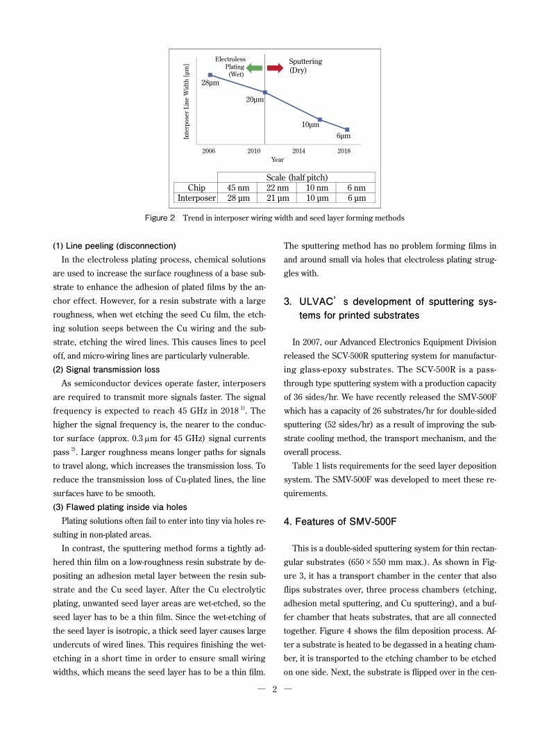
Figure 1 shows an interposer structure and its fabrica-
tion process. An interposer has a core substrate (a glass
epoxy substrate with copper films), on both sides of which
are resin layers (build-up films) and Cu wiring layers al-
ternately laminated to form four to six layers in total. Up-
per and lower wiring layers are connected with Cu via
holes. Since the interposer substrate is made by laminat-
ing wiring layers, it is also known as the build-up sub-
strate. A method called the semi-additive process (SAP) is
used for micro-wiring. The SAP process uses electrolytic
plating for Cu wiring only. This process consists of the fol-
lowing steps: forming a seed layer (electroless plating or
sputtering), forming wiring patterns by using photoresist,
Cu wiring by electrolytic plating, resist stripping, and
etching unwanted seed layers.
2. Deposition of seed layers by sputtering
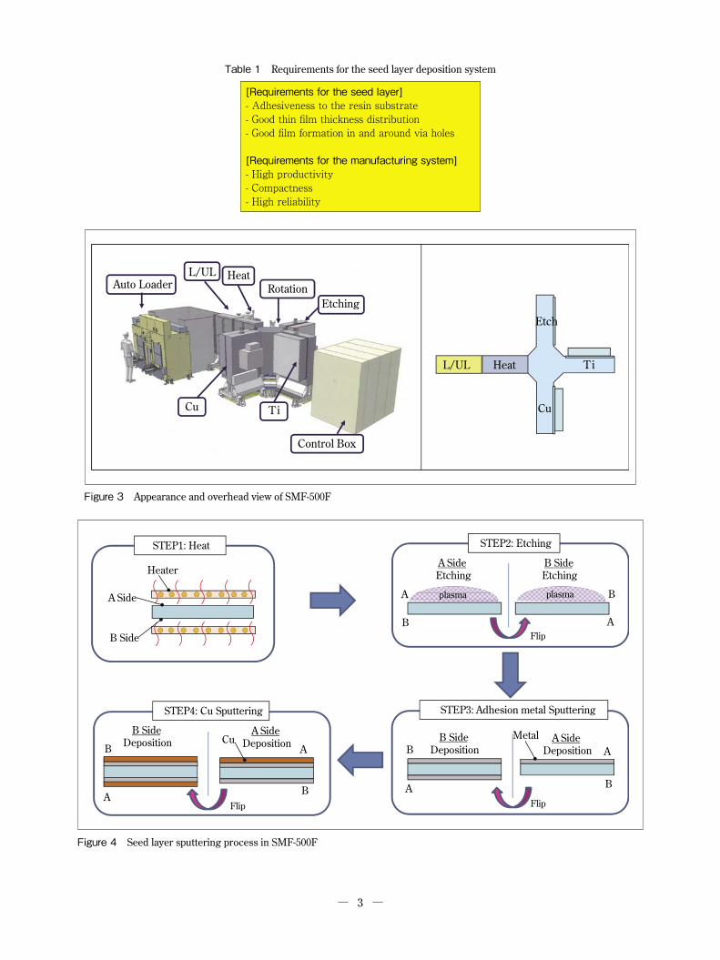
As technologies for micro-wiring chips and high-density
chip packaging advance today, the interposer wiring also
needs to be micro-fabricated. Figure 2 shows a roadmap
of interposer wire line widths and seed layer forming
methods. Electroless plating, which is a wet process, is
used to form interposer seed layers whose line width is 20
μm or larger. It does not work for smaller widths, so the
sputtering process is used instead. This is because the
electroless plating has the following problems when it
comes to micro-wiring:
ULVAC TECHNICAL JOURNAL No.77E 2013
Sputtering System SMV-500F for Manufacturing Printed Substrates
Eriko Mase*, Harunori Iwai*, Kouji Takahashi*, Tetsushi Fujinaga**, Masahiro Matsumoto**, Makoto Arai** and Atsuhito Ihori**
* Advanced Electronics Equipment Division, ULVAC, Inc.** Institute for Super Materials, ULVAC, Inc.
Figure 1 Manufacturing process of an interposer (SAP)
2
(1) Line peeling (disconnection)In the electroless plating process, chemical solutions
are used to increase the surface roughness of a base sub-
strate to enhance the adhesion of plated films by the an-
chor effect. However, for a resin substrate with a large
roughness, when wet etching the seed Cu film, the etch-
ing solution seeps between the Cu wiring and the sub-
strate, etching the wired lines. This causes lines to peel
off, and micro-wiring lines are particularly vulnerable.
(2) Signal transmission lossAs semiconductor devices operate faster, interposers
are required to transmit more signals faster. The signal
frequency is expected to reach 45 GHz in 2018 1). The
higher the signal frequency is, the nearer to the conduc-
tor surface (approx. 0.3 μm for 45 GHz) signal currents
pass 2). Larger roughness means longer paths for signals
to travel along, which increases the transmission loss. To
reduce the transmission loss of Cu-plated lines, the line
surfaces have to be smooth.
(3) Flawed plating inside via holesPlating solutions often fail to enter into tiny via holes re-
sulting in non-plated areas.
In contrast, the sputtering method forms a tightly ad-
hered thin film on a low-roughness resin substrate by de-
positing an adhesion metal layer between the resin sub-
strate and the Cu seed layer. After the Cu electrolytic
plating, unwanted seed layer areas are wet-etched, so the
seed layer has to be a thin film. Since the wet-etching of
the seed layer is isotropic, a thick seed layer causes large
undercuts of wired lines. This requires finishing the wet-
etching in a short time in order to ensure small wiring
widths, which means the seed layer has to be a thin film.
The sputtering method has no problem forming films in
and around small via holes that electroless plating strug-
gles with.
3. ULVAC’s development of sputtering sys-tems for printed substrates
In 2007, our Advanced Electronics Equipment Division
released the SCV-500R sputtering system for manufactur-
ing glass-epoxy substrates. The SCV-500R is a pass-
through type sputtering system with a production capacity
of 36 sides/hr. We have recently released the SMV-500F
which has a capacity of 26 substrates/hr for double-sided
sputtering (52 sides/hr) as a result of improving the sub-
strate cooling method, the transport mechanism, and the
overall process.
Table 1 lists requirements for the seed layer deposition
system. The SMV-500F was developed to meet these re-
quirements.
4. Features of SMV-500F
This is a double-sided sputtering system for thin rectan-
gular substrates (650×550 mm max.). As shown in Fig-
ure 3, it has a transport chamber in the center that also
flips substrates over, three process chambers (etching,
adhesion metal sputtering, and Cu sputtering), and a buf-
fer chamber that heats substrates, that are all connected
together. Figure 4 shows the film deposition process. Af-
ter a substrate is heated to be degassed in a heating cham-
ber, it is transported to the etching chamber to be etched
on one side. Next, the substrate is flipped over in the cen-
Figure 2 Trend in interposer wiring width and seed layer forming methods
3
[Requirements for the seed layer]- Adhesiveness to the resin substrate- Good thin film thickness distribution- Good film formation in and around via holes
[Requirements for the manufacturing system]- High productivity- Compactness- High reliability
Table 1 Requirements for the seed layer deposition system
Figure 3 Appearance and overhead view of SMF-500F
Figure 4 Seed layer sputtering process in SMF-500F

4
tral reversing chamber before being carried into the etch-
ing chamber again for the other side to be etched. Then,
after passing through the reversing chamber, it is trans-
ferred into the adhesion metal sputtering chamber where
it is sputtered on both sides through steps similar to the
etching process. Finally, the substrate enters the Cu sput-
tering chamber to be processed on both sides. The SMV-
500F has the following five features:
(1) High adhesiveness; excellent film thickness distri-
bution
(2) Deposition at low temperatures
(3) High productivity
(4) Small footprint
(5) Substrate holding mechanism for thin substrates
(substrate holder)
Details on each item are described below:
(1) The SMV-500F achieves an adhesion strength of 0.8
kgf/cm or more for a Ti/Cu seed film deposited on a
build-up material for the SAP process by heating the
substrate before sputtering, the surface treatment,
and our original adhesion layer sputtering process.
Also it employs a multi-magnet cathode to ensure the
thickness distributions of the adhesion metal (Ti) and
Cu films are within±5% per 500-mm square area.
(2) The build-up material properties require a low-temper-
ature process, 150℃ or lower. The SMV-500F deposits
films at low temperatures by employing an electrostat-
ic chuck 3) for cooling substrates.
(3) The SMV-500F shows high performance in cooling
substrates with its electrostatic chuck, which enables
low-temperature deposition at high power, so its film
deposition time is about half that of the SCV-500R, a
conventional pass-through type sputtering system.
Also, since the SMV-500F has a substrate reversing-
cum-transport chamber at the center, it can flip and
transport a substrate at the same time in a vacuum to
perform double-sided film deposition in a short time.
(4) Employing an electrostatic chuck enables stationary
deposition for both the adhesion metal layer and the
Cu film. For this reason, one chamber is designed for
the adhesion metal layer, and another for Cu, and this
system has fewer chambers than conventional in-line
sputtering systems. Consequently, the equipment foot-
print is about half of a typical in-line system.
(5) The substrate holding method is important for thin
substrate vertical transport and double-sided film de-
position systems. The SMV-500F employs a substrate
holder that can set substrates without producing wrin-
kles or slack.
5. Conclusion
We have already accepted orders for SMV-500F sys-
tems from leading overseas manufacturers. Our demo
systems have provided a number of domestic and over-
seas customers with the experience of using the system.
Printed substrate manufacturers have changed their seed
layer deposition method from electroless plating to sput-
tering in their ongoing development and test production
of packaging for micro-wired chips. Since we have already
carried out many experiments for customers with this sys-
tem, we expect the SMV-500F to become the standard
model in the industry by 2014 when the mass-production
of interposers for micro-wired chips is supposed to start.
Among our future goals, the development of the best
process conditions for each base material is first priority.
Responding to the trend of micro-wiring, material manu-
facturers are launching new materials of various surface
roughness levels and thermal expansion coefficients one
after another. We need to develop processes for these ma-
terials.
Also, to promote the advantageous dry process, we
need to reduce its cost. For that reason, we are now devel-
oping new seed layer materials and cathodes that ensure
more efficient target consumption.
In addition, we are developing etching/ashing equip-
ment for rectangular thin substrates and PECVD systems
as well. We aim at providing total solutions for manufac-
turing printed substrates.
References and patents
1)ITRS2010 Update, Assembly and Packaging
2)Yoshihiro Konishi, “Microwave Technology,” Nikkan
Kogyo Shinbun, 2001
3)Japanese Patent Application No. 2013-019767 “Thin
Substrate Processing System”
5
1. Introduction
The market demand for vehicles that use inverters and
switching power supply devices, such as HEV (hybrid
electric vehicles) and EV (electric vehicles), and energy
saving home appliances (such as air conditioners for Chi-
na and developing countries, and power conditioners for
solar and wind power generation) is increasing. Along
with this, the market for power devices that are used for
them, such as IGBT (insulated gate bipolar transistors)
and MOS-FET (metal oxide semiconductor field effect
transistors), is also rapidly growing.
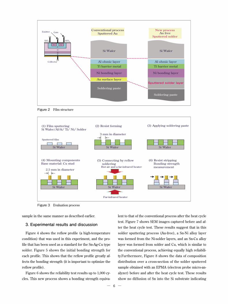
The backside electrode of these power devices forms
an ohmic contact with the Si substrate and a solder con-
nection to the heat radiation substrate. Its typical multi-
film structure consists of, from the Si substrate side, (1)
an Al or silicide ohmic contact layer, (2) a Ti barrier metal
layer, (3) a Ni bonding layer, and (4) an Au layer (100 to
200 nm) for preventing surface oxidation and improving
the solder wettability. In the current device manufacturing
process, after this electrode film is formed by sputtering
or vacuum evaporation, a solder film of required thickness
is vapor deposited or printed in air with another device,
and then the electrode is connected to the radiator by re-
flow soldering. However, due to the recent steep rise in
the price of precious metals, new processes for making
this Au film on the electrode thinner and alternative mate-
rials to replace Au are being studied now. We have studied
a high-reliability low-cost process that deposits a solder
layer by sputtering in a vacuum after forming a Ni film in
the same chamber, which will replace Au as an oxidation
preventive film.
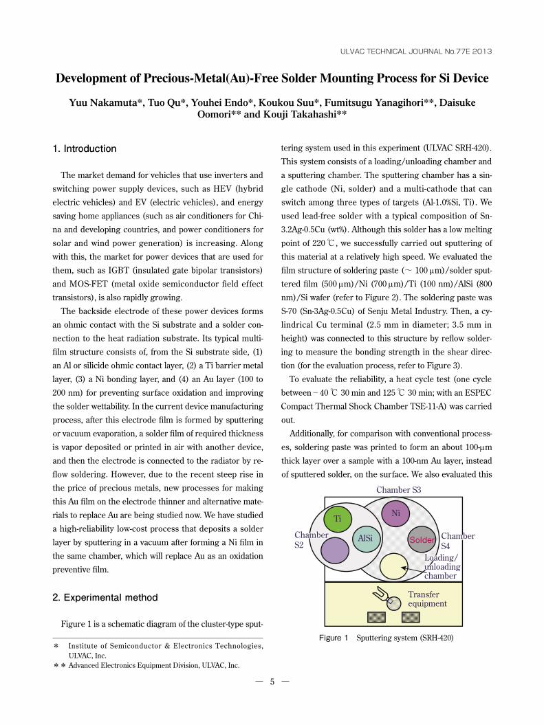
2. Experimental method
Figure 1 is a schematic diagram of the cluster-type sput-
tering system used in this experiment (ULVAC SRH-420).
This system consists of a loading/unloading chamber and
a sputtering chamber. The sputtering chamber has a sin-
gle cathode (Ni, solder) and a multi-cathode that can
switch among three types of targets (Al-1.0%Si, Ti). We
used lead-free solder with a typical composition of Sn-
3.2Ag-0.5Cu (wt%). Although this solder has a low melting
point of 220 ℃, we successfully carried out sputtering of
this material at a relatively high speed. We evaluated the
film structure of soldering paste (~ 100 μm)/solder sput-
tered film (500 μm)/Ni (700 μm)/Ti (100 nm)/AlSi (800
nm)/Si wafer (refer to Figure 2). The soldering paste was
S-70 (Sn-3Ag-0.5Cu) of Senju Metal Industry. Then, a cy-
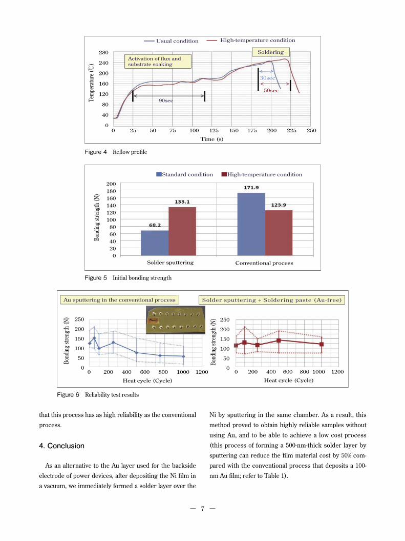
lindrical Cu terminal (2.5 mm in diameter; 3.5 mm in
height) was connected to this structure by reflow solder-
ing to measure the bonding strength in the shear direc-
tion (for the evaluation process, refer to Figure 3).
To evaluate the reliability, a heat cycle test (one cycle
between-40 ℃ 30 min and 125 ℃ 30 min; with an ESPEC
Compact Thermal Shock Chamber TSE-11-A) was carried
out.
Additionally, for comparison with conventional process-
es, soldering paste was printed to form an about 100-μm
thick layer over a sample with a 100-nm Au layer, instead
of sputtered solder, on the surface. We also evaluated this
ULVAC TECHNICAL JOURNAL No.77E 2013
Development of Precious-Metal(Au)-Free Solder Mounting Process for Si Device
Yuu Nakamuta*, Tuo Qu*, Youhei Endo*, Koukou Suu*, Fumitsugu Yanagihori**, Daisuke Oomori** and Kouji Takahashi**
* Institute of Semiconductor & Electronics Technologies, ULVAC, Inc.
** Advanced Electronics Equipment Division, ULVAC, Inc.
Figure 1 Sputtering system (SRH-420)
6
sample in the same manner as described earlier.
3. Experimental results and discussion
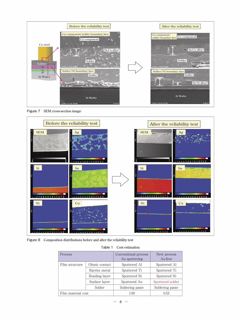
Figure 4 shows the reflow profile (a high-temperature
condition) that was used in this experiment, and the pro-
file that has been used as a standard for the Sn-Ag-Cu type
solder. Figure 5 shows the initial bonding strength for
each profile. This shows that the reflow profile greatly af-
fects the bonding strength (it is important to optimize the
reflow profile).
Figure 6 shows the reliability test results up to 1,000 cy-
cles. This new process shows a bonding strength equiva-
lent to that of the conventional process after the heat cycle
test. Figure 7 shows SEM images captured before and af-
ter the heat cycle test. These results suggest that in this
solder sputtering process (Au-free), a Sn-Ni alloy layer
was formed from the Ni-solder layers, and an Sn-Cu alloy
layer was formed from solder and Cu, which is similar to
the conventional process, achieving equally high reliabili-
ty.Furthermore, Figure 8 shows the data of composition
distribution over a cross-section of the solder sputtered
sample obtained with an EPMA (electron probe micro-an-
alyzer) before and after the heat cycle test. These results
show no diffusion of Sn into the Si substrate indicating
Collector
Emitter Gate
P+N +
N-P
N+N+
SiO2 SiO2
Si Wafer
Al ohmic layer
Ti barrier metal
Ni bonding layer
Au surface layer
Soldering paste
従来プロセスAuスパッタ
Conventional processSputtered Au
Sputtered solder layer
Si Wafer
Al ohmic layer
Ti barrier metal
Ni bonding layer
Soldering paste
新プロセスAuレス
はんだスパッタ
New processAu free
Sputtered solder
Figure 2 Film structure
(1) Film sputteringSi Wafer/Al-Si/ Ti/ Ni/ Solder
(2) Resist forming
3 mm in diameter
(3) Applying soldering paste
(4) Mounting componentsBase material: Cu stud
2.5 mm in diameter
(5) Connecting by reflow soldering
Hot air and a far-infrared heater
(6) Resist stripping Bonding strength measurement
Sputtered film
Si Wafer Si Wafer
Si Wafer
Si Wafer
Si WaferSi Wafer
Far-infrared heater
Figure 3 Evaluation process
7
that this process has as high reliability as the conventional
process.
4. Conclusion
As an alternative to the Au layer used for the backside
electrode of power devices, after depositing the Ni film in
a vacuum, we immediately formed a solder layer over the
Ni by sputtering in the same chamber. As a result, this
method proved to obtain highly reliable samples without
using Au, and to be able to achieve a low cost process
(this process of forming a 500-nm-thick solder layer by
sputtering can reduce the film material cost by 50% com-
pared with the conventional process that deposits a 100-
nm Au film; refer to Table 1).
Bond
ing
stren
gth
(N)
■標準条件 ■高温条件■Standard condition ■High-temperature condition
200180160140120100
80604020
0Solder sputtering Conventional process
Figure 5 Initial bonding strength
Solder sputtering + Soldering paste (Au-free)
0 200 400 600 800 1000 1200
Heat cycle (Cycle)
0 200 400 600 800 1000 1200
Heat cycle (Cycle)
250
200
150
100
50
0
Bond
ing
stren
gth
(N)250
200
150
100
50
0
Bond
ing
stren
gth
(N)
Au sputtering in the conventional process
Figure 6 Reliability test results
Activation of flux and substrate soaking
90sec
30sec
50sec
Soldering
0 25 50 75 100 125 150 175 200 225 250
Time (s)
280
240
200
160
120
80
40
0
Tem
pera
ture
(℃)
High-temperature conditionUsual condition
Figure 4 Reflow profile
8
Figure 7 SEM cross-section image
Ni
SEM
Si
Cu
Ag
Sn
Ni
SEM
Si
Cu
Ag
Sn
Before the reliability test After the reliability test
Figure 8 Composition distributions before and after the reliability test
Table 1 Cost estimation
Process Conventional processAu sputtering
New processAu-free
Film structure Ohmic contact Sputtered Al Sputtered AlBarrier metal Sputtered Ti Sputtered TiBonding layer Sputtered Ni Sputtered NiSurface layer Sputtered Au Sputtered solder
Solder Soldering paste Soldering pasteFilm material cost 1.00 0.53
?
Solder
0.7μ
mSolder
?
?
Solder
Solder
?
9
1. Introduction
Along with the advancement of mobile data terminals
such as smartphones, increasingly larger amounts of data
are transmitted through the Internet, and there is a grow-
ing demand for high-speed, low-power-consumption, and
high density memory devices. However, flash memory,
which is a typical non-volatile memory, has not fully satis-
fied the market demand due to its disadvantages, such as
its high operation voltage, low rewrite speed, and small
number of rewritable cycles. The development of types of
memory that do not have these shortcomings is being
called for. Today, various types of memory, such as Ferro-
electric Random Access Memory (FeRAM), Magnetore-
sistive Random Access Memory (MRAM), Phase Change
Memory (PCRAM), Resistance Random Access Memory
(ReRAM), have been proposed and are the subjects of
much research.
Of these memory types, ReRAM has an operation volt-
age of 3 V or lower, is rewritten in nano seconds, with-
stands 1010 or more rewrite cycles, has a cell area of 4F2,
can be three-dimensional, and can be a multivalued mem-
ory. ReRAM is one of the promising candidates for a non-
volatile memory that can make up for the shortcomings of
flash memory and reduce cost per bit 1), 2).
However, it has been said that it is too difficult to mass-
produce ReRAM because there remains unknown mecha-
nisms of how it works.
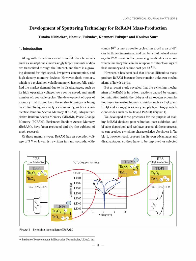
But a recent study revealed that the switching mecha-
nism of ReRAM is in redox reactions caused by oxygen
ion migration inside the bi-layer of an oxygen accumula-
tion layer (near-stoichiometric oxides such as Ta2O5 and
HfO2) and an oxygen vacancy supply layer (oxygen-defi-
cient oxides such as TaOx and PCMO) (Figure 1).
We developed three processes for the purpose of mak-
ing ReRAM devices: post-reduction, post-oxidation, and
bi-layer deposition; and we have proved all these process-
es can produce switching characteristics. As shown in Ta-
ble 1, however, each process has its own advantages and
disadvantages, so they have to be improved or selected
ULVAC TECHNICAL JOURNAL No.77E 2013
Development of Sputtering Technology for ReRAM Mass-Production
Yutaka Nishioka*, Natsuki Fukuda*, Kazunori Fukuju* and Koukou Suu*
* Institute of Semiconductor & Electronics Technologies, ULVAC, Inc.
Figure 1 Switching mechanism of ReRAM
10
Table 1
Process type Advantages Disadvantages
Post-reduction- Can be used to produce three-dimensional devices.- Low-temperature process- A small number of processes
- Hard to control oxygen composition.
Post-oxidation - Can be used to produce three-dimensional devices.
- High-temperature process- Larger number of processes- For ALD and CVD, it is hard to control oxygen amounts in an oxygen deficient layer.
Bi-layer deposition - The amount of oxygen can be easily controlled by the sputtering method.
- Larger number of processes- For ALD and CVD, it is hard to control oxygen amounts in an oxygen deficient layer.
Figure 2 Schematic diagram of ULVAC’s original dielectric film sputtering module
Figure 3 Film thickness and sheet resistance uniformities over the wafer surface
11
according to device requirements in the future.
This paper selects TaOx as an example from among the
various oxide materials being studied in our group to
present ReRAM device fabrication methods by the three
processes of post-reduction, post-oxidation, and bi-layer
deposition, and shows the switching characteristics of
samples made by them. This paper also describes their
advantages, disadvantages, and future trends.
2. Experimental method
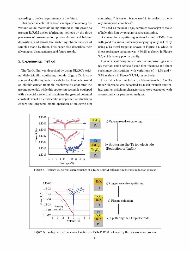
The Ta2O5 film was deposited by using ULVAC’s origi-
nal dielectric film sputtering module (Figure 2). In con-
ventional sputtering systems, a dielectric film is deposited
on shields causes unstable discharge by changing the
ground potential, while this sputtering system is equipped
with a special anode that maintains the ground potential
constant even if a dielectric film is deposited on shields, to
ensure the long-term stable operation of dielectric film
sputtering. This system is now used in ferroelectric mem-
ory mass-production lines3).
We used Ta metal or Ta2O5 ceramics as a target to make
a TaOx thin film by oxygen-reactive sputtering.
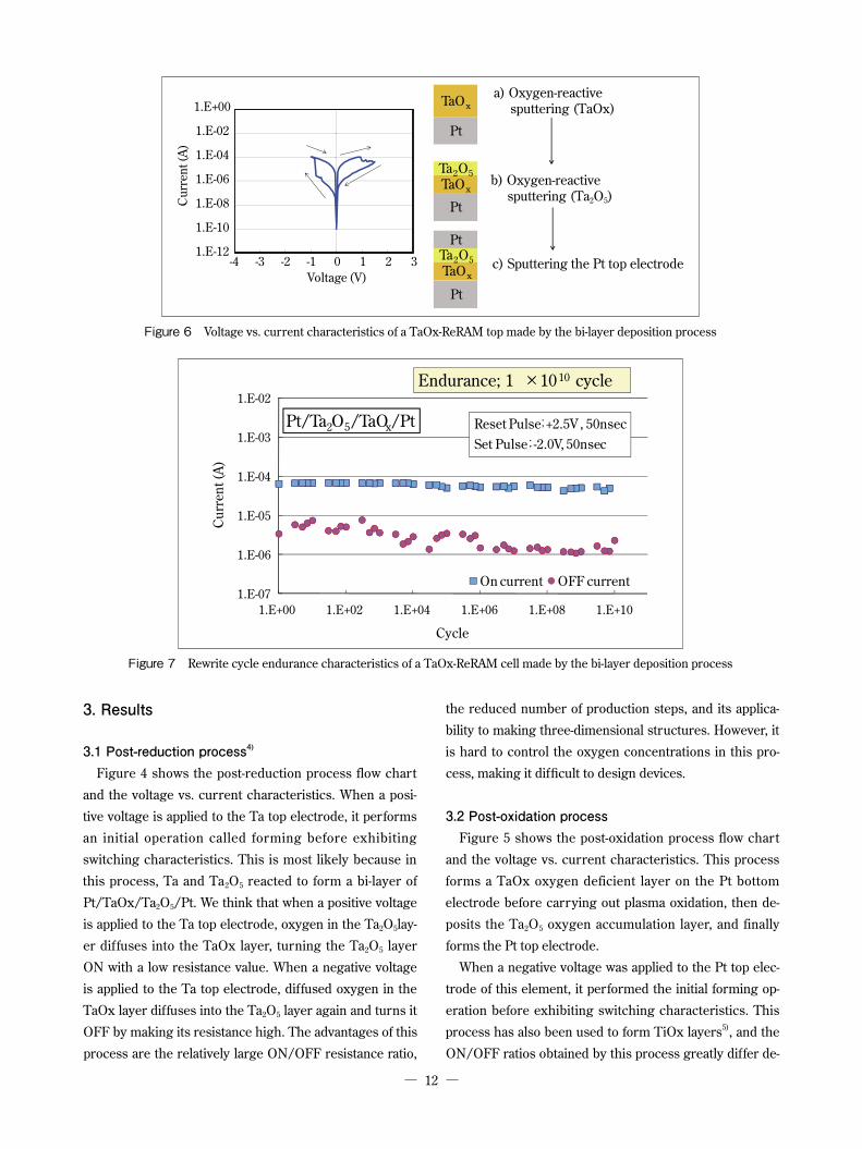
A conventional sputtering system formed a TaOx film
with good thickness uniformity varying by only ±4.5% by
using a Ta metal target as shown in Figure 3-1, while its
sheet resistance variation was ±30.2% as shown in Figure
3-2, which is very poor in quality.
Our new sputtering system used an improved gas sup-
ply method, and it achieved good film thickness and sheet
resistance distributions with variations of ±4.5% and±3.3% as shown in Figure 3-3, 3-4, respectively.
On a TaOx film thus formed, a 50-μm-diameter Pt or Ta
upper electrode was deposited by mask-through sputter-
ing, and its switching characteristics were evaluated with
a semiconductor parameter analyzer.
Figure 4 Voltage vs. current characteristics of a TaOx-ReRAM cell made by the post-reduction process
Figure 5 Voltage vs. current characteristics of a TaOx-ReRAM cell made by the post-oxidation process
12
3. Results
3.1 Post-reduction process4)
Figure 4 shows the post-reduction process flow chart
and the voltage vs. current characteristics. When a posi-
tive voltage is applied to the Ta top electrode, it performs
an initial operation called forming before exhibiting
switching characteristics. This is most likely because in
this process, Ta and Ta2O5 reacted to form a bi-layer of
Pt/TaOx/Ta2O5/Pt. We think that when a positive voltage
is applied to the Ta top electrode, oxygen in the Ta2O5lay-
er diffuses into the TaOx layer, turning the Ta2O5 layer
ON with a low resistance value. When a negative voltage
is applied to the Ta top electrode, diffused oxygen in the
TaOx layer diffuses into the Ta2O5 layer again and turns it
OFF by making its resistance high. The advantages of this
process are the relatively large ON/OFF resistance ratio,
the reduced number of production steps, and its applica-
bility to making three-dimensional structures. However, it
is hard to control the oxygen concentrations in this pro-
cess, making it difficult to design devices.
3.2 Post-oxidation processFigure 5 shows the post-oxidation process flow chart
and the voltage vs. current characteristics. This process
forms a TaOx oxygen deficient layer on the Pt bottom
electrode before carrying out plasma oxidation, then de-
posits the Ta2O5 oxygen accumulation layer, and finally
forms the Pt top electrode.
When a negative voltage was applied to the Pt top elec-
trode of this element, it performed the initial forming op-
eration before exhibiting switching characteristics. This
process has also been used to form TiOx layers5), and the
ON/OFF ratios obtained by this process greatly differ de-
Figure 7 Rewrite cycle endurance characteristics of a TaOx-ReRAM cell made by the bi-layer deposition process
Figure 6 Voltage vs. current characteristics of a TaOx-ReRAM top made by the bi-layer deposition process
13
pending on the material. The advantage is that it can be
applied to the production of three-dimensional devices,
but its operating voltage has to be decreased further.
3.3 Bi-layer deposition process6)
Figure 6 shows the bi-layer deposition process flow
chart and the voltage vs. current characteristics. This pro-
cess forms the TaOx oxygen deficient layer on a Pt sub-
strate by oxygen-reactive sputtering, then deposits the
near-stoichiometric Ta2O5 layer, and finally forms the Pt
upper electrode. The cell obtained by this process per-
forms switching with a low current and a low voltage. This
cell performs switching with a reset current of 70 μA, well
under 200 μA, which is required for micro-fabricating
transistors. Figure 7 shows the rewrite endurance test re-
sults for this cell. This cell endures more than 1010 rewrite
cycles maintaining its ON current at less than 70 μA,
which is equivalent to the excellent characteristics of heat-
proof and reliability reported by Z. Wei, et al1).
Consequently, the ReRAM cell made by the bi-layer de-
position process operates at low-voltage, has a high re-
write speed, and has excellent rewrite endurance, elimi-
nating the shortcomings of flash memories.
4. Conclusion
We used three processes, post-reduction, post-oxida-
tion, and bi-layer deposition, to fabricate ReRAM cells in
this experiment. The cell made by the bi-layer deposition
process showed excellent characteristics that would be
good enough to replace flash memories. These character-
istics are also good enough to be used for the structure of
one transistor and one memory, which is supposed to be
used in the early stages of ReRAM mass-production.
To reduce cost per bit, three-dimensional devices need
to be developed in the future. This suggests that it is im-
portant to develop ALD/CVD technologies, ReRAM char-
acteristic control technologies by the post-reduction and
post-oxidation processes, and three-dimensionally fabri-
cated bi-directional diode and three-dimensional transis-
tors.
References
1) Z. Wei, et al., IEDM Tech. Dig., p.721-724(2011)T.
Uchida: Jpn. J. Appl. Phys., 33(1994)L43 [8]
2) S. Kawabata, et al., IMW2010, p60
3) Koukou Suu, et al. TECHNICAL REPORT OF IEICE.
ED2000-69, SDM2000-69(200-06), p49-56
4) Natsuki Fukuda, et al., Mater. Res. Symp. Proc.
Vol.1250-G12-12, 2010 Materials Research Society
5) Yutaka Nishioka, et al. , ULVAC TECHNICAL
JOURNAL No.67, 2007
6) Natsuki Fukuda, et al., Mater. Res. Soc. Symp. Proc.
Vol. 1430-E3-16, 2012 Materials Research Society
14
1. Introduction
Electric vehicles (EV) are drawing interest because
they discharge no CO2. EVs have been put on the market
since the 1970s, but have never caught on. Fuji Heavy In-
dustries (Plug-in Stella), Mitsubishi Motors (i-MiEV), and
Nissan Motor (LEAF) started EV sales in 2009, and they
are beginning to spread thanks to the growing environ-
mental consciousness among people. EVs currently on
the market can travel up to 90 to 160 km on a full charge,
after which they have to be recharged. They can be
charged at home in fourteen hours at 100 VAC and seven
to eight hours at 200 VAC with a typical charger. EVs are
being advertised as inexpensive to charge when going
shopping nearby, which is one of the main ways a car is
used, as it can be done at home. However, quick chargers
that can charge EVs in a short amount of time are neces-
sary for users who do not have charging equipment at
home, and for long-distance driving. The Ministry of
Economy, Trade and Industry announced that an estimat-
ed 5,000 quick charger units are to be installed by 2020.
Currently, 50-kW models that can charge an EV to 80% in
20 to 30 min and 20 to 30-kW models that can charge to
80% in 40 min are commercially available.
ULVAC’s environmental policy is “Develop products
with a goal to save energy, reduce the use of natural re-
sources and contribute to the conservation of our environ-
ment.” We entered into the quick charger industry in
2010, and have delivered 60 units to date.
To quickly put our model on the market, ULVAC’s cur-
rent EVQC-5000 Series quick charger products use exist-
ing devices such as motor control inverters from Reliance
Electric Limited, an affiliate company. After that, their
market prices fell sharply, and today are about half of the
initial price. In order to meet market demand, we devel-
oped the EVQC-7000 Series with the aim of reducing the
cost by half again.
2. How quick chargers work
An EV runs by consuming electric energy stored in its
internal battery. When it runs out of stored energy, it can
be recharged by being connected to a 100 VAC or 200
VAC outlet (it is recommended that an outlet designed as
charging equipment be used). However, it is not reason-
able to use all the contract power at an ordinary house for
charging a car, so the charging current at 100 VAC or 200
VAC is restricted. It is for this reason that the charging
time is so long.
The quick charger is designed to charge a car in a short
amount of time. Although a quick charge can be per-
formed by using a heavy current, overheating the battery
must be avoided, so when it is charged to a certain per-
centage, the charging current is decreased to keep the
ULVAC TECHNICAL JOURNAL No.77E 2013
Development of the EVQC-7000 Series Quick Charging Station
Takeo Toda*
* Reliance Electric Limited
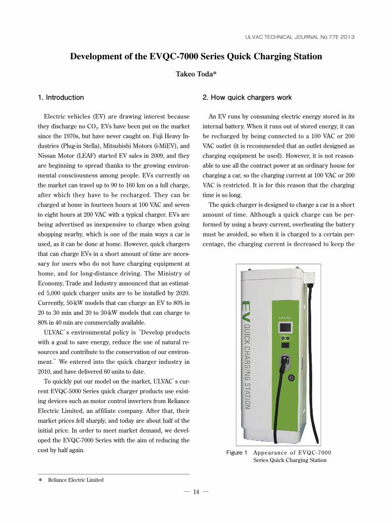
Figure 1 Appearance of EVQC-7000 Series Quick Charging Station
15
voltage within a specified range. As only the EV knows
the condition of the battery, the quick charger communi-
cates with the EV and charges the battery according to
commands from the EV. If different manufacturers sup-
plied devices incompatible to each other, the whole sys-
tem would not work, so a standard has been established
by the CHAdeMO association, whose membership in-
cludes companies from the power, automobile, charger,
and other industries. Charging from empty to 80% takes
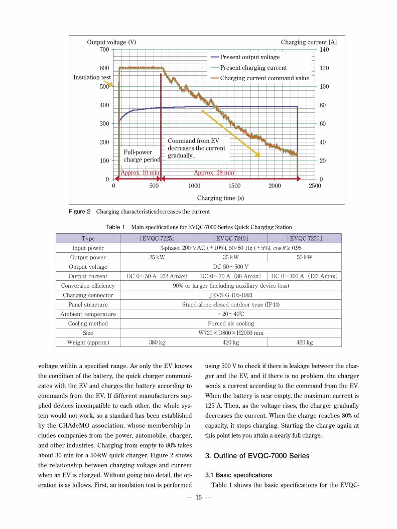
about 30 min for a 50-kW quick charger. Figure 2 shows
the relationship between charging voltage and current
when an EV is charged. Without going into detail, the op-
eration is as follows. First, an insulation test is performed
using 500 V to check if there is leakage between the char-
ger and the EV, and if there is no problem, the charger
sends a current according to the command from the EV.
When the battery is near empty, the maximum current is
125 A. Then, as the voltage rises, the charger gradually
decreases the current. When the charge reaches 80% of
capacity, it stops charging. Starting the charge again at
this point lets you attain a nearly full charge.
3. Outline of EVQC-7000 Series
3.1 Basic specificationsTable 1 shows the basic specifications for the EVQC-
Table 1 Main specifications for EVQC-7000 Series Quick Charging Station
Type 「EVQC-7225」 「EVQC-7240」 「EVQC-7250」Input power 3-phase, 200 VAC (±10%), 50/60 Hz (±5%), cosθ≥ 0.95
Output power 25 kW 35 kW 50 kWOutput voltage DC 50~500 VOutput current DC 0~50 A(62 Amax) DC 0~70 A(88 Amax) DC 0~100 A(125 Amax)
Conversion efficiency 90% or larger (including auxiliary device loss)Charging connector JEVS G 105-1993
Panel structure Stand-alone closed outdoor type (IP44)Ambient temperature -20~40℃
Cooling method Forced air coolingSize W720×D800×H2000 mm
Weight (approx.) 380 kg 420 kg 460 kg
Figure 2 Charging characteristicsdecreases the current
16
7000 Series. There are three types: 50 kW, 25 kW, and 35
kW. The external sizes of these three are the same, be-
cause the capacity is determined by the number of inter-
nal power modules.
3.2 Product conceptWe established the following two product concepts and
started the development of the EVQC-7000 Series
(1) Low cost(2) User friendly charger
Since the biggest problem with the current EVQC-5000
Series is its price, we focused on the following points to
reduce cost:
i) Use smaller components
Employing a high switching frequency for the power
generation circuit made components smaller. Details will
be described later.
ii) Select inexpensive components at the manufacturer’s plant
We had manufacturing this product overseas (in China
in particular) in mind at the start of development. Compa-
nies from many countries hold production bases in China.
Manufacturers in China, including OEM businesses, capi-
talized by Japanese, European, or American companies
are producing components that are up to global standards
in terms of technology and quality. These components are
inexpensive because of the worldwide competition. Not
only using these components, but employing housing
components such as metal plates that are easily obtained
in China greatly helps reduce cost. However, what manu-
facturers and components are available is not known in Ja-
pan. With the help of ULVAC Automation Technology
(Shanghai) Corporation, we searched for suitable compo-
nents in China and our development team members regu-
larly visited component and metal plate manufacturers in
China to find reliable companies and establish procure-
ment channels. These efforts enabled us to use Chinese
made components and, although halfway through test
production, start manufacturing the products in China.
iii) Production independent of workers’ skills
We thought we should take into account the possibility
of frequent change of workers when operating a manufac-
turing business overseas. For this reason, we minimized
work tasks that require a person’s skills such as welding
and adjustments.
iv) Reduction in manufacturing man-hours
Although modularization increases the number of cir-
cuits, it decreases the current in each part making it easy
to design substrates. By mounting as many components
as possible on substrates, we decreased the number of
cumbersome wiring and assembling steps to reduce the
required man-hours. Wireless signal transmission was
employed for part of the communications between mod-
ules to reduce the amount of wiring required for commu-
nication signals.
The “User friendly charger” design policy includes the
following points. Since this product is for EVs, the design
should be environmentally friendly, and we thought it
should also be user friendly because these chargers are
used by the general public.
i) Enhanced user interface
A motion sensor and an illuminance sensor are used to
illuminate the operating panel with an LED light when a
person stands in front of the charger at night. Voice guid-
ance and a touch panel are provided as well.
ii) Improved appearance design
To make the screen and the appearance attractive to as
many people as possible, we asked an industrial designer
to design the appearance. The outer case is rounded, and
the operating panel area is painted green suggesting the
environment.
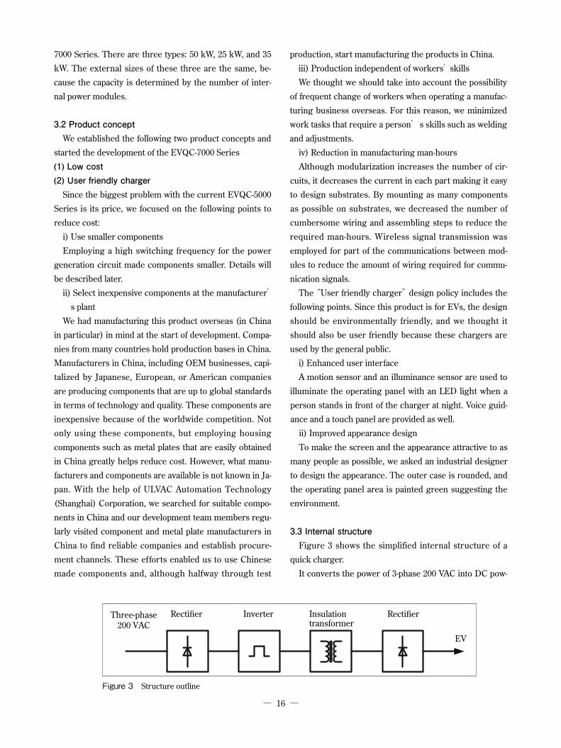
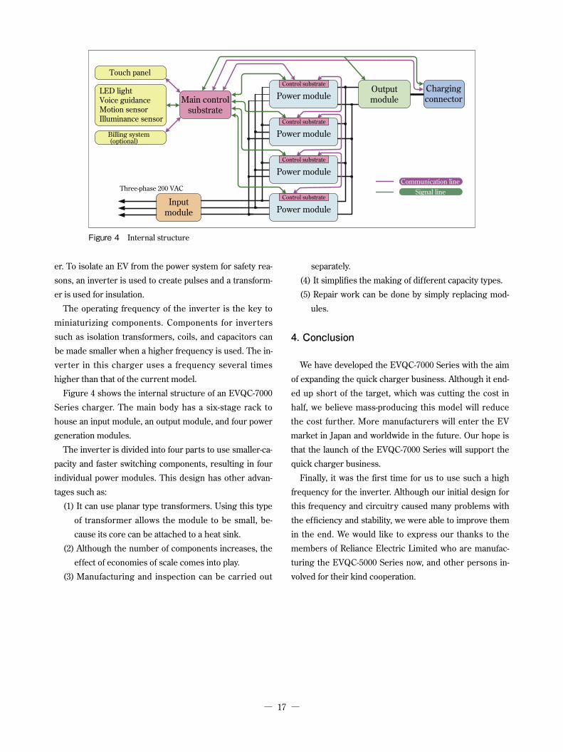
3.3 Internal structureFigure 3 shows the simplified internal structure of a
quick charger.
It converts the power of 3-phase 200 VAC into DC pow-
Figure 3 Structure outline
17
er. To isolate an EV from the power system for safety rea-
sons, an inverter is used to create pulses and a transform-
er is used for insulation.
The operating frequency of the inverter is the key to
miniaturizing components. Components for inverters
such as isolation transformers, coils, and capacitors can
be made smaller when a higher frequency is used. The in-
verter in this charger uses a frequency several times
higher than that of the current model.
Figure 4 shows the internal structure of an EVQC-7000
Series charger. The main body has a six-stage rack to
house an input module, an output module, and four power
generation modules.
The inverter is divided into four parts to use smaller-ca-
pacity and faster switching components, resulting in four
individual power modules. This design has other advan-
tages such as:
(1) It can use planar type transformers. Using this type
of transformer allows the module to be small, be-
cause its core can be attached to a heat sink.
(2) Although the number of components increases, the
effect of economies of scale comes into play.
(3) Manufacturing and inspection can be carried out
separately.
(4) It simplifies the making of different capacity types.
(5) Repair work can be done by simply replacing mod-
ules.
4. Conclusion
We have developed the EVQC-7000 Series with the aim
of expanding the quick charger business. Although it end-
ed up short of the target, which was cutting the cost in
half, we believe mass-producing this model will reduce
the cost further. More manufacturers will enter the EV
market in Japan and worldwide in the future. Our hope is
that the launch of the EVQC-7000 Series will support the
quick charger business.
Finally, it was the first time for us to use such a high
frequency for the inverter. Although our initial design for
this frequency and circuitry caused many problems with
the efficiency and stability, we were able to improve them
in the end. We would like to express our thanks to the
members of Reliance Electric Limited who are manufac-
turing the EVQC-5000 Series now, and other persons in-
volved for their kind cooperation.
Three-phase 200 VAC
Power module
Inputmodule
Control substrateOutputmodule
Communication line
Chargingconnector
Touch panel
LED lightVoice guidanceMotion sensorIlluminance sensor
Billing system (optional)
Main controlsubstrate
Signal line
Power moduleControl substrate
Power moduleControl substrate
Power moduleControl substrate
Figure 4 Internal structure
18
1. Introduction
X-ray Photoelectron Spectroscopy (XPS) also known as
Electron Spectroscopy for Chemical Analysis (ESCA)
measures the energy distribution of photoelectrons emit-
ted from a sample that is irradiated with x-rays.XPS spec-
tra provide elemental and chemical state compositional in-
formation from the surface of the sample being analyzed.
For many high performance materials, the surface plays a
critical role in how well the material performs. Therefore,
when developing or manufacturing high performance ma-
terials with thin film structures or chemically active sur-
faces, such as catalysts, it is important to be able to char-
acterize the surface composition and correlate it with
performance. The average depth of analysis for an XPS
measurement is a few nanometers, and for a surface anal-
ysis technique, XPS provides excellent quantification and
the ability to successfully analyze most solid materials.
For these reasons, XPS has become the most widely used
surface analysis technique and plays a critical role in the
research and development of new high performance ma-
terials. In the manufacturing industries, XPS is also used
to understand surface related problems such as adhesion,
to identify surface defects or stains, and to verify the com-
position of modified surfaces and thin film structures.For
some high performance materials, the composition of the
surface is so critical to their performance that XPS is used
to routinely monitor a manufacturing process and ensure
product quality.
Today, the XPS user community is very large and a di-
verse range of capabilities is being sought by the XPS
market. Attempting to meet these needs drives improve-
ments in XPS instrument performance, the development
of new accessories, and the development of custom instru-
ments to meet the specific needs of individual users. Ex-
amples of specialized needs include: the development of
catalytic reactors to study catalyst surfaces in a controlled
environment; and the development of vacuum transfer
vessels to provide a controlled environment to bring high-
ly reactive surfaces such as Li battery materials into XPS
instruments. Broader based needs lead to the develop-
ment of new technology that is incorporated into our XPS
instruments. Examples include: the development of a ras-
ter scanned micro-focused x-ray source for high sensitivi-
ty micro area XPS analysis1); the development of a turnkey
neutralization scheme for the automated analysis of insu-
lating materials2); developing C603) and Ar2500 gas cluster4)
ion guns to make it possible to characterize polymer and
organic thin film structures.
Since the introduction of commercial XPS instruments,
there has been a need to develop or provide an expert to
operate the instrument and interpret the data. This need
ULVAC TECHNICAL JOURNAL No.77E 2013
PHI X-tool: A Fully Automated XPS Microprobe
Risayo Inoue, Tetsuro Shirao, Seiji Koizumi and Noriaki Sanada
* ULVAC-PHI, Inc.
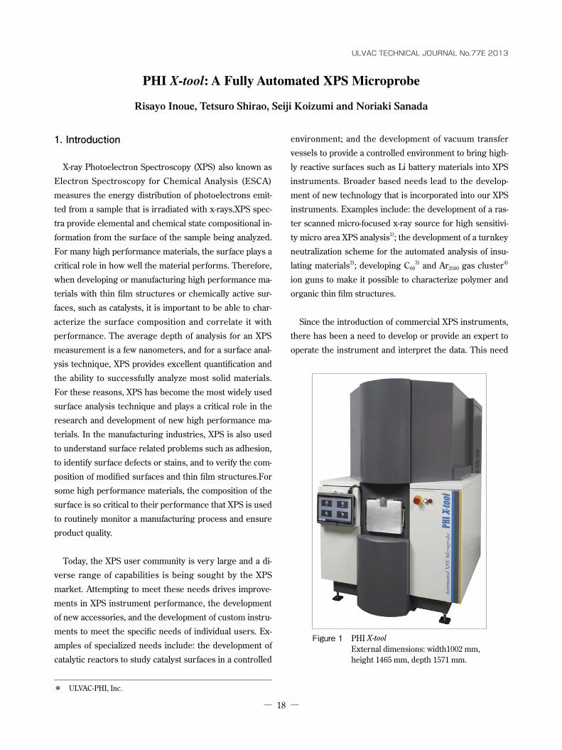
Figure 1 PHI X-tool External dimensions: width1002 mm, height 1465 mm, depth 1571 mm.
19
for specialized skills to use an XPS instrument has limited
the expansion of the use of XPS5). In an effort to remove
this barrier for using XPS, we have developed a new XPS
product, the PHI X-tool, which reduces the level of special-
ized skills needed perform an XPS measurement. The X-
tool has the basic XPS performance characteristics of our
high-end XPS machines, but is designed for a non-expert
XPS user to obtain routine XPS measurements with guid-
ance from a unique and easy to use software interface. In
the following pages, we will introduce the new X-tool to
you.
2. PHI X-tool
A photograph of the PHI X-tool is shown in Fig. 1. The X-tool is a highly automated XPS system that has a com-
pact sleek design. The user only interacts with the sample
introduction chamber to introduce, and remove samples
and the touch screen used to initiate a measurement.
2.1 PHI X-tool FeaturesThe main features of PHI X-tool are described below.
Those features marked with an asterisk (*) are unique
features introduced to the XPS market on the X-tool.
1) Simple to use XPS with a tablet user interfacea. The first surface analysis instrument with a tablet as
the user interface*
b. Unique touch screen software completes measure-
mentswith three touch based choices*
c. User interface software available in four languages:
Japanese, English, Chinese, and Korean*
2) Automatic measurement and automatic reporting capabilities
a. Automated sample introduction, analysis, and report
generation
b. Automated data reduction including quantification
and curve-fitting results
c. The first XPS instrument with automatic scheduled
maintenance notifications*
d. Automated system baking, hardware alignment, and
energy axis calibration
3) Equipped with PHI’s state of the art hardwarea. PHI’s unique micro focused scanning x-ray source
with a 20 µm minimum beam diameter
b. Three types of sample observation: introduction
chamber camera, live camera view, and x-ray beam
induced secondary electron imaging (SXI)*
c. Fast mapping mode with scanning x-ray beam
d. Large area stage driven mapping mode
While having the basic performance characteristics of
PHI’s high end XPS instruments, the PHI X-tool is a sin-
gle-techniqueinstrumentwithout the scalability of PHI’s
other XPS instruments. Reviewing ULVAC-PHI’s XPS
product line: The Quantera II is an automated XPS micro-
probe with PHI’s highest XPS performance and limited
scalability, the VersaProbe II is a laboratory XPS system
with a high degree of scalability and many optional acces-
sories that can be added to it, and the X-tool is single pur-
pose easy to use XPS instrument for routine large and
small area XPS measurements.It is our vision for the fu-
ture that the X-tool will expand the use of XPS by reducing
the expertise required to use an XPS instrument, and
make it possible for more students in universities and
more staff in the industrial world to have access to XPS
equipment and the information it can provide to help them
with their work.
2.2 Overview of PHI X-tool operationFrom the X-tool’s touch panel menu, a usercan select ei-
ther the Recipe Acquire mode or the Normal Acquire
Mode of operation. The Recipe Acquire mode is used
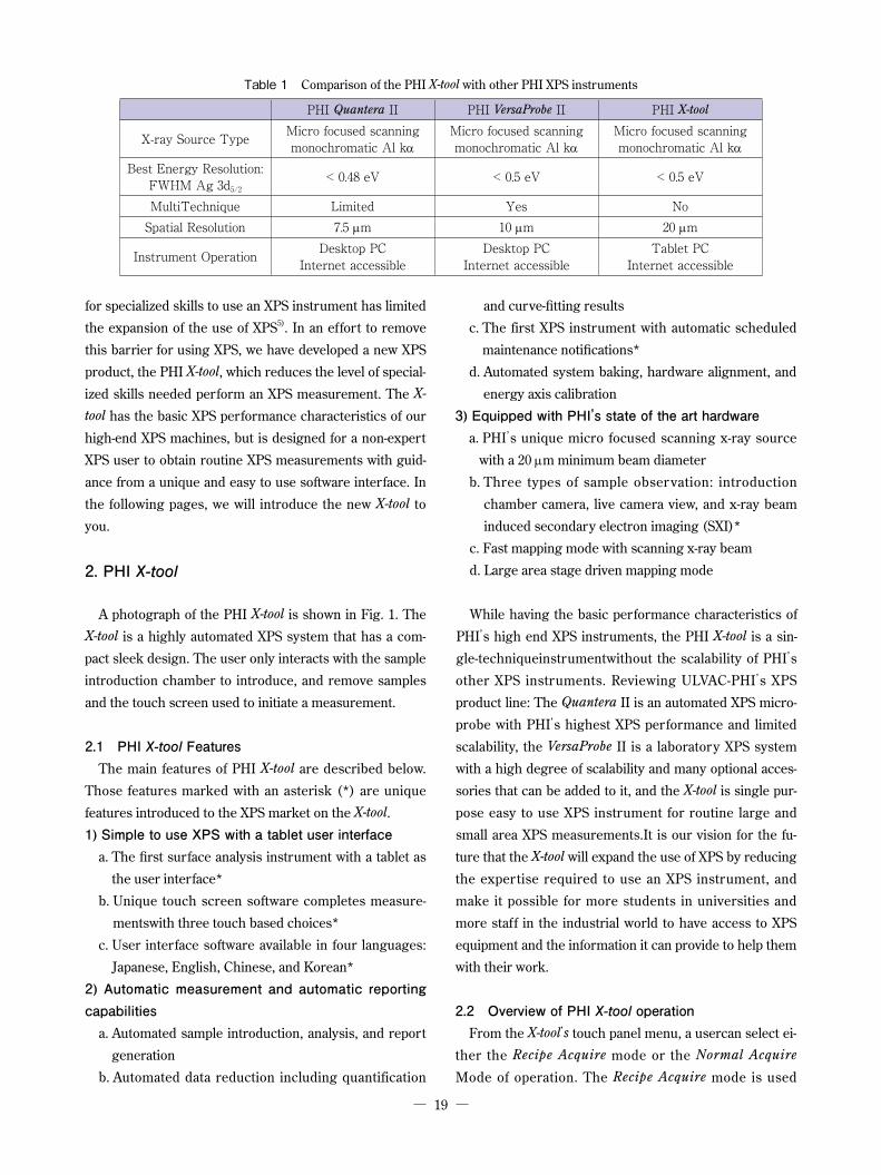
Table 1 Comparison of the PHI X-tool with other PHI XPS instruments
PHI Quantera II PHI VersaProbe II PHI X-tool
X-ray Source Type Micro focused scanning monochromatic Al kα
Micro focused scanning monochromatic Al kα
Micro focused scanning monochromatic Al kα
Best Energy Resolution: FWHM Ag 3d5/2
< 0.48 eV < 0.5 eV < 0.5 eV
MultiTechnique Limited Yes NoSpatial Resolution 7.5 µm 10 µm 20 µm
Instrument Operation Desktop PCInternet accessible
Desktop PCInternet accessible
Tablet PCInternet accessible
20
when the same measurement will be made multiple times
and the recipe for the measurement is predefined. In the Normal Mode, the user defines the instrument conditions
for each measurement.The following example provides an
overview of how the Recipe Acquire mode is used to per-
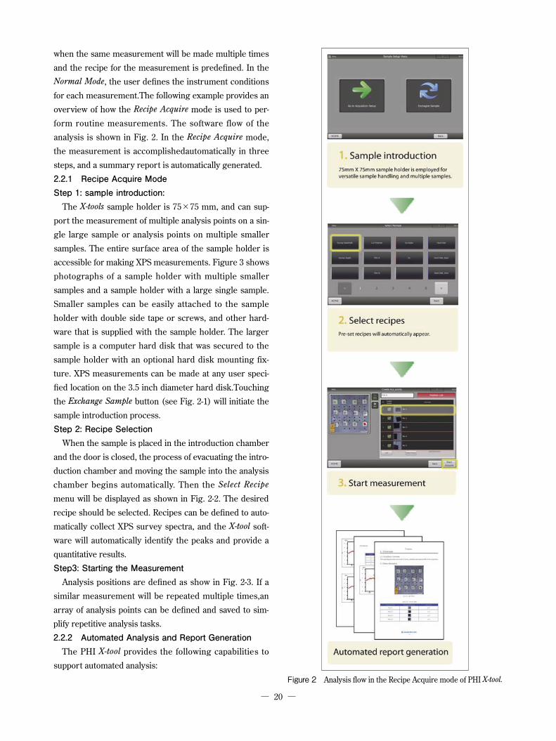
form routine measurements. The software flow of the
analysis is shown in Fig. 2. In the Recipe Acquire mode,
the measurement is accomplishedautomatically in three
steps, and a summary report is automatically generated.
2.2.1 Recipe Acquire ModeStep 1: sample introduction:
The X-tools sample holder is 75×75 mm, and can sup-
port the measurement of multiple analysis points on a sin-
gle large sample or analysis points on multiple smaller
samples. The entire surface area of the sample holder is
accessible for making XPS measurements. Figure 3 shows
photographs of a sample holder with multiple smaller
samples and a sample holder with a large single sample.
Smaller samples can be easily attached to the sample
holder with double side tape or screws, and other hard-
ware that is supplied with the sample holder. The larger
sample is a computer hard disk that was secured to the
sample holder with an optional hard disk mounting fix-
ture. XPS measurements can be made at any user speci-
fied location on the 3.5 inch diameter hard disk.Touching
the Exchange Sample button (see Fig. 2-1) will initiate the
sample introduction process.
Step 2: Recipe SelectionWhen the sample is placed in the introduction chamber
and the door is closed, the process of evacuating the intro-
duction chamber and moving the sample into the analysis
chamber begins automatically. Then the Select Recipe
menu will be displayed as shown in Fig. 2-2. The desired
recipe should be selected. Recipes can be defined to auto-
matically collect XPS survey spectra, and the X-tool soft-
ware will automatically identify the peaks and provide a
quantitative results.
Step3: Starting the MeasurementAnalysis positions are defined as show in Fig. 2-3. If a
similar measurement will be repeated multiple times,an
array of analysis points can be defined and saved to sim-
plify repetitive analysis tasks.
2.2.2 Automated Analysis and Report GenerationThe PHI X-tool provides the following capabilities to
support automated analysis:
Figure 2 Analysis flow in the Recipe Acquire mode of PHI X-tool.
21
Using these capabilities, it is possible to completely au-
tomate the analysis and reporting of routine repetitive
XPS measurements. When performing failure analysis or
analyzing an unknown sample, the analyst can use the
same capabilities to locate the desired analysis area and
program an automated analysis of the selected area.
For the Automatic Qualitative analysis mode, we devel-
oped a new peak identification algorithm that provides a
more robust peak identification capability. As a result, it
has become possible to identify the major constituent ele-
ments with a high success rate,enabling the automatic
qualitative and quantitative analysis of samples with un-
known surface compositions.
For repetitive measurements, such as a film thickness
measurement, the appropriate measurement conditions
and the desired analysis locations can be predefined and
stored as a setting that can be recalled for use in the X-
tool’s Recipe Analysis mode of operation. When the auto-
mated analysis is complete, the X-tool’s software can be
configured to send an e-mail notification to the analyst.
3. Applications
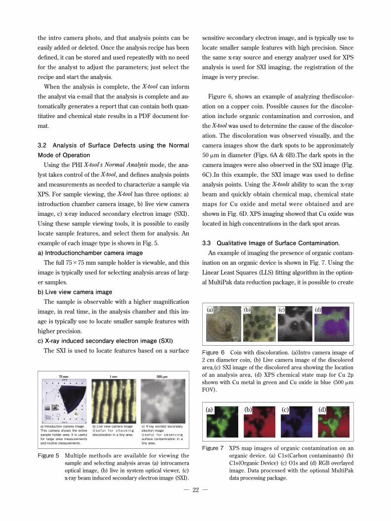
3.1 Example of the use of Recipe Analysis modefor quality control.
For quality control applications, the same measurement
will be made multiple times from multiple samples to pro-
vide timely feedback in support of a manufacturing pro-
cess. Shown in Fig. 4 is an intro camera image with multi-
ple samples that can be programmed for a single
automated analysis to evaluate the surface treatment of
the samples. Shown in figure four are 21 samples that
were attached to the sample holder with double sided
tape. As discussed in 2-2 section, a custom analysis recipe
andthe locations of analysis can preprogrammed and acti-
vated with a single touch on the tablets screen. It should
be noted that the analysis points were predefined using
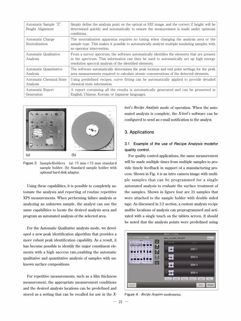
Figure 4 Recipe Acquire modemenu.
Figure 3 SampleHolders (a) 75 mm×75 mm standard sample holder. (b) Standard sample holder with optional hard disk adaptor.
Automatic Sample “Z” Height Alignment
Simply define the analysis point on the optical or SXI image, and the correct Z height will be determined quickly and automatically to ensure the measurement is made under optimum conditions.
Automatic Charge Neutralization
The neutralization apparatus requires no tuning when changing the analysis area or the sample type. This makes it possible to automatically analyze multiple insulating samples with no operator intervention.
Automatic Qualitative Analysis
From a survey spectrum, the software automatically identifies the elements that are present in the spectrum. This information can then be used to automatically set up high energy resolution spectral analysis of the identified elements.
Automatic Quantitative Analysis
The software automatically determines the peak location and end point settings for the peak area measurements required to calculate atomic concentrations of the detected elements.
Automatic Chemical State Analysis
Using predefined recipes, curve fitting can be automatically applied to provide detailed chemical state information.
Automatic Report Generation
A report containing all the results is automatically generated and can be presented in English, Chinese, Korean, or Japanese languages.
22
the intro camera photo, and that analysis points can be
easily added or deleted. Once the analysis recipe has been
defined, it can be stored and used repeatedly with no need
for the analyst to adjust the parameters; just select the
recipe and start the analysis.
When the analysis is complete, the X-tool can inform
the analyst via e-mail that the analysis is complete and au-
tomatically generates a report that can contain both quan-
titative and chemical state results in a PDF document for-
mat.
3.2 Analysis of Surface Defects using the Normal Mode of Operation
Using the PHI X-tool’s Normal Analysis mode, the ana-
lyst takes control of the X-tool, and defines analysis points
and measurements as needed to characterize a sample via
XPS. For sample viewing, the X-tool has three options: a)
introduction chamber camera image, b) live view camera
image, c) x-ray induced secondary electron image (SXI).
Using these sample viewing tools, it is possible to easily
locate sample features, and select them for analysis. An
example of each image type is shown in Fig. 5.
a) Introductionchamber camera imageThe full 75×75 mm sample holder is viewable, and this
image is typically used for selecting analysis areas of larg-
er samples.
b) Live view camera imageThe sample is observable with a higher magnification
image, in real time, in the analysis chamber and this im-
age is typically use to locate smaller sample features with
higher precision.
c) X-ray induced secondary electron image (SXI)The SXI is used to locate features based on a surface
sensitive secondary electron image, and is typically use to
locate smaller sample features with high precision. Since
the same x-ray source and energy analyzer used for XPS
analysis is used for SXI imaging, the registration of the
image is very precise.
Figure 6, shows an example of analyzing thediscolor-
ation on a copper coin. Possible causes for the discolor-
ation include organic contamination and corrosion, and
the X-tool was used to determine the cause of the discolor-
ation. The discoloration was observed visually, and the
camera images show the dark spots to be approximately
50 µm in diameter (Figs. 6A & 6B).The dark spots in the
camera images were also observed in the SXI image (Fig.
6C).In this example, the SXI image was used to define
analysis points. Using the X-tools ability to scan the x-ray
beam and quickly obtain chemical map, chemical state
maps for Cu oxide and metal were obtained and are
shown in Fig. 6D. XPS imaging showed that Cu oxide was
located in high concentrations in the dark spot areas.
3.3 Qualitative Image of Surface Contamination.An example of imaging the presence of organic contam-
ination on an organic device is shown in Fig. 7. Using the
Linear Least Squares (LLS) fitting algorithm in the option-
al MultiPak data reduction package, it is possible to create
Figure 5 Multiple methods are available for viewing the sample and selecting analysis areas (a) introcamera optical image, (b) live in system optical viewer, (c)x-ray beam induced secondary electron image (SXI).
a) Introduction camera imageThis camera shows the entire sample holder area. It is useful for large area measurements and routine measurements.
b) Live view camera imageU s e f u l f o r c h e c k i n g discoloration in a tiny area.
c) X-ray excited secondary electron imageU s e f u l f o r o b s e r v i n g surface contamination in a tiny area.
Figure 6 Coin with discoloration. (a)Intro camera image of 2 cm diameter coin, (b) Live camera image of the discolored area,(c) SXI image of the discolored area showing the location of an analysis area, (d) XPS chemical state map for Cu 2p shown with Cu metal in green and Cu oxide in blue (500 µm FOV).
Figure 7 XPS map images of organic contamination on an organic device. (a) C1s(Carbon contaminants) (b) C1s(Organic Device) (c) O1s and (d) RGB overlayed image. Data processed with the optional MultiPak data processing package.

23
images of multiple chemical states based on changes in
peak shape versus location in the image. In this example,
LLS fitting was applied to a C 1s image. The contamina-
tion was not optically visible, and attempts to observe the
image with SEM/EDS failed due to chemical damage
caused by the high energy electron beam. However, using
the XPS capabilities of the X-tool, the contamination was
observed, and imaged to show the spatial distribution of
the contaminant with islands that were approximately 100
µm in diameter.
4. Summary
In 2012, ULVAC-PHI and Physical Electronics shipped
XPS instruments to companies, universities, and public in-
stitutions in twelve countries including: Japan, East Asia,
Southeast Asia, South Asia, Middle East, Europe, North
America, and Latin America. Since XPS is becoming a
widely used analytical technique in many countries, in ed-
ucation and manufacturing sites, an increasing demand
exists for the XPS instruments with both high perfor-
mance and user-friendliness that can be used by a broader
group of people that are not surface analysis experts.
The PHI X-tool is an instrument that is focused on pro-
viding the essential capabilities of XPS, with high a cost/
performance ratio. We expect the X-tool will increase the
use of XPS by providing and instrument with a very intui-
tive user interface that will make it possible for non-ex-
perts to use XPS on a routine basis.
References
1) H. Iwai, R. Oiwa, P. E. Larson and M. Kudo, Appl.
Surf. Sci., 100/101, (1996) 283.
2) P. E. Larson and M. A. Kelly, J. Vac. Sci. Technol. A16
(1998) 3483.
3) N. Sanada, A. Yamamoto, R. Oiwa and Y. Ohashi,
Surf. Interface Anal., 36 (2004) 280.
4) T. Miyayama, N. Sanada, M. Suzuki, J. S. Hammond,
S.-Q.D. Si and A.Takahara, J. Vac. Sci. Technol. A28
(2010) L1.
5) Repor t on the Competitiveness of the Japanese
Analytical Instruments Industry, National Institute
of Advanced Industrial Science and Technology,
AIST11-B000006-1 (2011).
24
1. Introduction
The ef fects of the Great East Japan Earthquake in
March 2011 on the Fukushima Daiichi Nuclear Power Sta-
tion revealed the vulnerabilities of energy supply in Japan.
Since the operation of several nuclear power plants was
stopped, power is being supplied for the time being by in-
creasing the operating rate of thermal power stations
while seeking for alternatives to nuclear power that pro-
vide a stable high volume with low cost supply. Because
one of the disadvantages of fossil energy including ther-
mal power is CO2 emissions, natural energies such as
wind and solar power are gathering attention. However,
there are many issues such as the scale of power genera-
tion and stability of supply.
Under such the circumstances, fuel cells are expected
to come into popular use as they are not af fected by
changes in the natural environment, can stably supply en-
ergy, and in theory do not emit CO2. In particular, the
polymer electrolyte fuel cell (PEFC) is a good alternative
for home and automobile applications. This is because
PEFCs are compact for a fuel cell and the safe operating
temperature range extends to as high as 100℃. However,
for spreading PEFCs, it is necessary to reduce the cost of
PEFCs themselves and establish the infrastructure for
them such as hydrogen stations. There have been many
attempts at cost reduction to achieve this end. For exam-
ple, replacing the expensive platinum catalyst material
with a non-platinum catalyst or changing the shape of the
platinum catalyst core shell to reduce the amount of plati-
num used. There is also an ambitious attempt to replace
the current wet catalyst manufacturing and support with
another method.
This article introduces the nanoparticle formation pulse
arc plasma source. This is a kind of dry catalyst manufac-
turing method where the target platinum is ionized
through vacuum pulse arc discharge and is then caused
to collide against the carrier. This method has significant
advantages. First, only several nanometers across of plati-
num corpuscles can be formed and evenly distributed
across the carrier. Also, the process is extremely easy to
perform. The catalyst material can be easily changed and
it is also possible to synthesize a catalyst material. This ar-
ticle introduces the principles of the nanoparticle forma-
tion pulse arc plasma source and reports the first attempt
to fabricate a platinum support carbon for fuel cells by us-
ing this device and assess its characteristics.
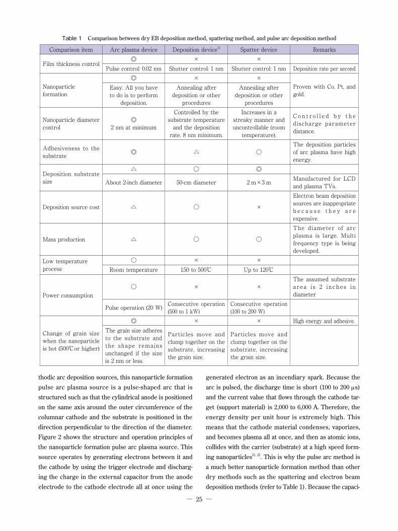
2. Principles of Nanoparticle Formation Pulse Arc Plasma SourceFigure 1 shows an overall view of the nanoparticle for-
mation pulse arc plasma source (Available from ULVAC-
RIKO, Inc. Product name: APD-1P Arc plasma method
nanoparticle formation device). Unlike normal DC ca-
ULVAC TECHNICAL JOURNAL No.77E 2013
Assessment of Platinum/Carbon Catalyst for Fuel Cell Created By Fabricuted Using a Nanoparticle Formation Pulse Arc Plasma Source
Yoshiaki Agawa*, Satoshi Endo*, Masamichi Matsuura* and Yoshikazu Ishii*
Figure 1 External view of the APD-1P Arc Plasma Method Nanoparticle Formation Device
* Development Department, ULVAC-RIKO, Inc.
25
thodic arc deposition sources, this nanoparticle formation
pulse arc plasma source is a pulse-shaped arc that is
structured such as that the cylindrical anode is positioned
on the same axis around the outer circumference of the
columnar cathode and the substrate is positioned in the
direction perpendicular to the direction of the diameter.
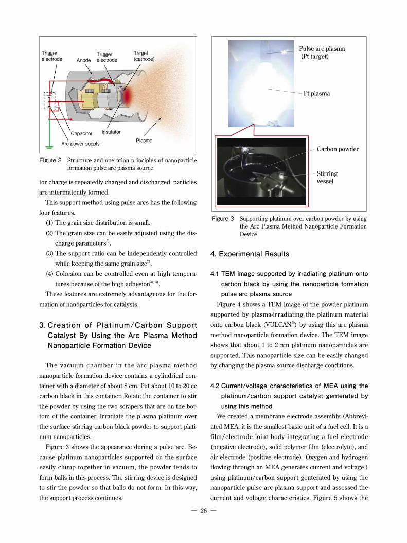
Figure 2 shows the structure and operation principles of
the nanoparticle formation pulse arc plasma source. This
source operates by generating electrons between it and
the cathode by using the trigger electrode and discharg-
ing the charge in the external capacitor from the anode
electrode to the cathode electrode all at once using the
generated electron as an incendiary spark. Because the
arc is pulsed, the discharge time is short (100 to 200 μs)
and the current value that flows through the cathode tar-
get (support material) is 2,000 to 6,000 A. Therefore, the
energy density per unit hour is extremely high. This
means that the cathode material condenses, vaporizes,
and becomes plasma all at once, and then as atomic ions,
collides with the carrier (substrate) at a high speed form-
ing nanoparticles1), 2). This is why the pulse arc method is
a much better nanoparticle formation method than other
dry methods such as the spattering and electron beam
deposition methods (refer to Table 1). Because the capaci-
Table 1 Comparison between dry EB deposition method, spattering method, and pulse arc deposition method
Comparison item Arc plasma device Deposition device1) Spatter device Remarks
Film thickness control◎ × ×
Pulse control: 0.02 nm Shutter control: 1 nm Shutter control: 1 nm Deposition rate per second
Nanoparticleformation
◎ × ×Proven with Co, Pt, and gold.
Easy. All you have to do is to perform
deposition.
Annealing after deposition or other
procedures
Annealing after deposition or other
procedures
Nanoparticle diameter control
◎2 nm at minimum
Controlled by the substrate temperature
and the deposition rate. 8 nm minimum.
Increases in a streaky manner and uncontrollable (room
temperature).
C o n t r o l l e d b y t h e discharge parameter distance.
Adhesiveness to the substrate ◎ △ ○
The deposition particles of arc plasma have high energy.
Deposition substrate size
△ ○ ◎
About 2-inch diameter 50-cm diameter 2 m×3 m Manufactured for LCD and plasma TVs.
Deposition source cost △ ○ ×
Electron beam deposition sources are inappropriate b e c a u s e t h e y a r e expensive.
Mass production △ ○ ○
The diameter of arc plasma is large. Multi frequency type is being developed.
Low temperatureprocess
○ × ×Room temperature 150 to 500℃ Up to 120℃
Power consumption○ × ×
The assumed substrate a rea i s 2 i nches i n diameter
Pulse operation (20 W) Consecutive operation (500 to 1 kW)
Consecutive operation (100 to 200 W)
Change of grain size when the nanoparticle is hot (500℃or higher)
◎ × × High energy and adhesive.The grain size adheres to the substrate and the shape remains unchanged if the size is 2 nm or less.
Particles move and clump together on the substrate, increasing the grain size.
Particles move and clump together on the substrate, increasing the grain size.
26
tor charge is repeatedly charged and discharged, particles
are intermittently formed.
This support method using pulse arcs has the following
four features.
(1) The grain size distribution is small.
(2) The grain size can be easily adjusted using the dis-
charge parameters2).
(3) The support ratio can be independently controlled
while keeping the same grain size2).
(4) Cohesion can be controlled even at high tempera-
tures because of the high adhesion3), 4).
These features are extremely advantageous for the for-
mation of nanoparticles for catalysts.
3. Creation of Platinum/Carbon Support Catalyst By Using the Arc Plasma Method Nanoparticle Formation Device
The vacuum chamber in the arc plasma method
nanoparticle formation device contains a cylindrical con-
tainer with a diameter of about 8 cm. Put about 10 to 20 cc
carbon black in this container. Rotate the container to stir
the powder by using the two scrapers that are on the bot-
tom of the container. Irradiate the plasma platinum over
the surface stirring carbon black powder to support plati-
num nanoparticles.
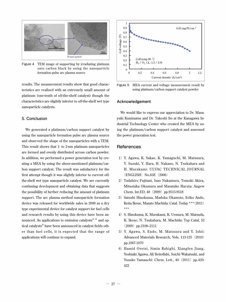
Figure 3 shows the appearance during a pulse arc. Be-
cause platinum nanoparticles supported on the surface
easily clump together in vacuum, the powder tends to
form balls in this process. The stirring device is designed
to stir the powder so that balls do not form. In this way,
the support process continues.
4. Experimental Results
4.1 TEM image supported by irradiating platinum onto carbon black by using the nanoparticle formation pulse arc plasma source
Figure 4 shows a TEM image of the powder platinum
supported by plasma-irradiating the platinum material
onto carbon black (VULCAN®) by using this arc plasma
method nanoparticle formation device. The TEM image
shows that about 1 to 2 nm platinum nanoparticles are
supported. This nanoparticle size can be easily changed
by changing the plasma source discharge conditions.
4.2 Current/voltage characteristics of MEA using the platinum/carbon support catalyst genterated by using this method
We created a membrane electrode assembly (Abbrevi-
ated MEA, it is the smallest basic unit of a fuel cell. It is a
film/electrode joint body integrating a fuel electrode
(negative electrode), solid polymer film (electrolyte), and
air electrode (positive electrode). Oxygen and hydrogen
flowing through an MEA generates current and voltage.)
using platinum/carbon support genterated by using the
nanoparticle pulse arc plasma support and assessed the
current and voltage characteristics. Figure 5 shows the
Figure 2 Structure and operation principles of nanoparticle formation pulse arc plasma source
Triggerelectrode Anode
Capacitor Insulator
PlasmaArc power supply
Triggerelectrode
Target(cathode)
Figure 3 Supporting platinum over carbon powder by using the Arc Plasma Method Nanoparticle Formation Device
27
results. The measurement results show that good charac-
teristics are realized with an extremely small amount of
platinum (one-tenth of off-the-shelf catalyst) though the
characteristics are slightly inferior to off-the-shelf wet type
nanoparticle catalysts.
5. Conclusion
We generated a platinum/carbon support catalyst by
using the nanoparticle formation pulse arc plasma source
and observed the shape of the nanoparticles with a TEM.
This result shows that 1- to 2-nm platinum nanoparticles
are formed and evenly distributed across carbon powder.
In addition, we performed a power generation test by cre-
ating a MEA by using the above-mentioned platinum/car-
bon support catalyst. The result was satisfactory for the
first attempt though it was slightly inferior to current off-
the-shelf wet type nanoparticle catalyst. We are currently
continuing development and obtaining data that suggests
the possibility of further reducing the amount of platinum
support. The arc plasma method nanoparticle formation
device was released for worldwide sales in 2009 as a dry
type experimental device for catalyst support for fuel cells
and research results by using this device have been an-
nounced. As applications to emission catalysts3), 4) and op-
tical catalysts6) have been announced in catalyst fields oth-
er than fuel cells, it is expected that the range of
applications will continue to expand.
Acknowledgement
We would like to express our appreciation to Dr. Masa-
yuki Kunimatsu and Dr. Takeshi Ito at the Kanagawa In-
dustrial Technology Center who created the MEA by us-
ing the platinum/carbon support catalyst and assessed
the power generation test.
References
1) Y. Agawa, K. Sakae, K. Yamaguchi, M. Matsuura,
Y. Suzuki, Y. Hara, H. Nakano, N. Tsukahara and
H. Murakami: ULVAC TECHNICAL JOURNAL
(ENGLISH)No.65E(2006)2) Tadahiro Fujitani, Isao Nakamura, Tomoki Akira,
Mitustaka Okumura and Masatake Haruta: Angew
Chem. Int.ED, 48(2009)pp.9515-9518
3) Satoshi Hinokuma, Madoka Okamoto, Eriko Ando,
Keita Ikeue, Masato Machida: Catal. Today ***(2011)***
4) S. Hinokuma, K. Murakami, K. Uemura, M. Matsuda,
K. Ikeue, N. Tsukahara, M. Machida: Top Catal, 52
(2009)pp.2108–2111
5) Y. Agawa, S. Endo, M. Matsuura and Y. Ishii:
Advanced Materials Research, Vols. 113-125(2010)pp.1067-1070
6) Hamid Oveisi, Simin Rahighi, Xiangfen Jiang,
Yoshiaki Agawa, Ali Beitollahi, Soichi Wakatsuki, and
Yusuke Yamauchi: Chem. Lett., 40(2011)pp.420-
422
Figure 5 MEA current and voltage measurement result by using platinum/carbon support catalyst powder
Figure 4 TEM image of supporting by irradiating platinum onto carbon black by using the nanopar ticle formation pulse arc plasma source
Arc Plasma Method Nanoparticle Formation Device
ULVAC RIKO, Inc.
Deposition of any material including metals, conductors, and semiconductors is supported.Deposition of any material including metals, conductors, and semiconductors is supported.
The pulse arc plasma source is a one-of-a-kind method that generates metal ions with simple processes and forms ultrathin films or nanoparticles.This source provides film flatness, formation of corpuscles and other effects that cannot be realized with other deposition methods!
Only electricity is required. Cooling water and discharge gas are unnecessary.The target size is about Φ 10 mm × L 17 mm.
Features
Sample creation example
Nanoparticle formation APD-P type
Metal nanoparticles on a substrate
Nanometer-level thin film
Amorphous carbon film of thick film
30 pulses20 pulses
20 pulses
Formation of alloy nanoparticles using two guns
Metal nanoparticles on an oxide particle
We will create samples for you. Please contact us.
Close-up
Film formation APD-S type
The grain size of the nanoparticles is determined by the relationshipbetween the discharge parameter and the base material.
The film thickness can be easily controlled from nm to µmby adjusting the pulse
Using a TEM to view a sample onto which cobalt had been deposed on a microgrid 10 times showed that 4- to 5-nm cobalt nanoparticles were evenly distributed.
5-nm scale bar and about 1.5-nm iron (black part) were repeatedly laminated. As 1.5 nm is deposed 20 times, the rate is about 0.075 nm/pulse.
When deposing amorphous carbon on a thick film, perform deposi-tion while decreasing the stress to prevent the film from peeling off. To produce a substrate from which the silicon and amorphous carbon film do not peel off, heat the substrate to 200℃.
Head Office: 1-9-19 Hakusan, Midori-ku, Yokohama, 226-0006, Japan Tel: +81-45-931-2285 (Operator) Fax: +81-45-933-9973Osaka Office: Uemura-Nissei Building, 3-3-31 Miyahara, Yodogawa-ku, Osaka, 532-0003, Japan Tel: +81-6-6397-2270 (Operator) Fax: +81-6-6397-1171
Arc voltage: 500 VCapacitor: 2,640 μFNumber of discharges: 1,650Substrate temperature: 200℃
TEM observation after deposing platinum and iron at the same time using two guns.Mainly 10-nm and 2-nm nanoparticles are both formed. When a 10-nm and 2-nm particle was analyzed with an EDX, iron and platinum signals were detected from each particle. Verifying that iron/platinum alloy nanoparticles had been formed.
Any deposition particle and base material can be used because nanoparticle formation with arc plasma guns results in physical absorption. Metal nanoparticles can even be attached onto oxides. In addition, deposition in the presence of oxygen allows you to attach oxide nanoparticles to oxide powder.
Gold/alumina Platinum/alumina
Multilayer film consisting of iron and carbon
Carbon
Silicon
2500 Hagisono, Chigasaki, Kanagawa, 253-8543, JapanTEL : (81) 467-89-2033 FAX : (81) 467-89-2250
JAPANULVAC, Inc.ULVAC TECHNO, Ltd.ULVAC KYUSHU CORPORATIONULVAC TOHOKU, Inc.ULVAC-RIKO, IncULVAC KIKO, Inc.Reliance Electric LimitedULVAC EQUIPMENT SALES, Inc.ULVAC CRYOGENICS INCORPORATEDULVAC-PHI, Inc.ULVAC COATING CORPORATIONSHOWA SHINKU CO., LTD.RAS Co., Ltd.TIGOLD Co.,Ltd.Nisshin SeigyoInitium, Inc.ULVAC ENGINEERING, Inc.ULVAC HUMAN RELATIONS, Ltd.Shinku Ceramics Co., Ltd.FINE SURFACE TECHNOLOGY CO.,LTD.
CHINAULVAC (China) Holding Co., Ltd.ULVAC (NINGBO) CO., LTDULVAC (SUZHOU) Co., Ltd.ULVAC Orient (Chengdu) Co., Ltd.ULVAC Automation Technology (Shanghai) CorporationULVAC Tianma Electric (Jing Jiang) Co., Ltd.ULVAC Vacuum Furnace (Shenyang) Co., Ltd.ULVAC CRYOGENICS(NINGBO) INCORPORATEDULVAC (Shanghai) Trading Co., Ltd.ULVAC NONFERROUS METALS (NINGBO) CO., LTD.ULVAC Materials (Suzhou) Co., Ltd.ULVAC Research Center SUZHOU Co., Ltd.ULVAC Opto-electronics Thin Film Technology (Shenzhen) Co., Ltd.Luoyang Xinyou Magnesium Co., LTDHong Kong ULVAC Co., Ltd.
U.S.AULVAC Technologies, Inc.Physical Electronics USA, Inc.
GERMANYULVAC GmbH
KOREAULVAC KOREA, Ltd.ULVAC Korea Precision, Ltd.Pure Surface Technology, Ltd.ULVAC CRYOGENICS KOREA INCORPORATEDUF TECH, Ltd.ULVAC Materials Korea, Ltd.
TAIWANULVAC TAIWAN Inc.ULTRA CLEAN PRECISION TECHNOLOGIES CORP.ULVAC SOFTWARE CREATIVE TECHNOLOGY, Co., Ltd.ULVAC Materials Taiwan, Inc.ULVAC AUTOMATION TAIWAN Inc.ULVAC Research Center TAIWAN, Inc.ULCOAT TAIWAN, Inc.
SINGAPOREULVAC SINGAPORE PTE LTD
THAILANDULVAC(THAILAND)LTD.
MALAYSIAULVAC MALAYSIA SDN. BHD.
INDIAULVAC, Inc. India Branch
Corporate Communications &IR Team Management PlanningDepartment ULVAC, Inc.
Related Documents