CD-P6000/CD-30 SERVICE MANUAL Compact Disc Player Effective : March, 2000 D00551700A CONTENTS 1 SPECIFICATIONS ・・・・・・・・・・・・・・・・・・・・・・・・・・・・・・・2 仕 様 2 ADJUSTMENT AND CHECKS ・・・・・・・・・・・・・・・・・・3 調整と確認 3 EXPLODED VIEWS AND PARTS LIST ・・・・・・・・・・6 分解図とパーツリスト 4 PC BOARDS AND PARTS LIST ・・・・・・・・・・・・・・・10 基板図とパーツリスト 5 INCLUDED ACCESSORIES ・・・・・・・・・・・・・・・・・・・13 付属品 6 BLOCK DIAGRAM ・・・・・・・・・・・・・・・・・・・・・・・・・・・・・14 ブロックダイアグラム

Welcome message from author
This document is posted to help you gain knowledge. Please leave a comment to let me know what you think about it! Share it to your friends and learn new things together.
Transcript

CCDD--PP66000000//CCDD--3300
SERVICE MANUAL
Compact Disc Player
Effective : March, 2000 D00551700A
CONTENTS
1 SPECIFICATIONS ・・・・・・・・・・・・・・・・・・・・・・・・・・・・・・・2仕 様
2 ADJUSTMENT AND CHECKS ・・・・・・・・・・・・・・・・・・3調整と確認
3 EXPLODED VIEWS AND PARTS LIST ・・・・・・・・・・6分解図とパーツリスト
4 PC BOARDS AND PARTS LIST ・・・・・・・・・・・・・・・10基板図とパーツリスト
5 INCLUDED ACCESSORIES ・・・・・・・・・・・・・・・・・・・13付属品
6 BLOCK DIAGRAM ・・・・・・・・・・・・・・・・・・・・・・・・・・・・・14ブロックダイアグラム

1 SPECIFICATIONS仕 様
2
CD-P6000/CD-30
CD-P6000
ピックアップ・システム .......................................... 光学式3ビームデジタルフィルター .............................. 8倍オーバーサンプリング周波数特性 .......................................... 20~20,000Hz(±0.5dB)エラー訂正方式 .......................................................................... CIRCSN比 .................................................................... 96dB以上(1kHz)全高調波歪率 ...................... 0.008%(1kHz、PitchControl Off)出力電圧........................................................................ 2±0.5Vrms電源...................................................................... 100V、50-60Hz消費電カ...................................................................................... 12W外形寸法(幅、高さ、奥行) ........................ 435×101×301mm重量............................................................................................ 4.5kg付属品.................................................................... 入出カコード(1)
リモートコントロールRC-728(1)乾電池(単4型)(2)
取扱説明書(1)保証書(1)
CD-30
ピックアップ・システム .......................................... 光学式3ビームデジタルフィルター .............................. 8倍オーバーサンプリング周波数特性 .......................................... 20~20,000Hz(±0.5dB)エラー訂正方式 .......................................................................... CIRCSN比 .................................................................... 96dB以上(1kHz)全高調波歪率 ...................... 0.008%(1kHz、PitchControl Off)出力電圧........................................................................ 2±0.5Vrmsヘッドホン出力 .............................................. 1±0.3Vrms(30Ω)電源...................................................................... 100V、50-60Hz消費電カ...................................................................................... 12W外形寸法(幅、高さ、奥行) ........................ 435×101×301mm重量............................................................................................ 4.5kg付属品............................................................ ピンプラグコード(1)
ラックマウント金具 L(1)ラックマウント金具 R(1)
各種ビス M3×12(4)、M5×12(4)M3用ワッシャー(4)M5用ワッシャー(4)
取扱説明書(1)機器保証書(1)
● 仕様および外観は、改善のため予告なく変更することがあります。
CD-P6000
Pickup: ......................................................3 beam tracking systemFrequency Response: ....................................20Hz - 20kHz ±0.5dBHarmonic Distortion: ........................................< 0.0015 % (1kHz)Signal-to-Noise Ratio (S/N): ............................> 96dB (1kHz, 0dB) Pitch Control: ........................................................................±12%Wow and Flutter: ........................................Below measurable limitPower Requirements:............................................230 V AC, 50 Hz Power Consumption: ..............................................................12 W Dimensions (W x H x D):................................435 x 101 x 301 mm Weight (net): ........................................................................4.5 kgStandard Accessories: ................Audio signal connection cord x 1
Wireless Remote Control Unit (RC-728)Battery (UM-4, "AAA", "R03" type) x 2
Owner's Manual x 1Warranty Card x 1
● Improvements may result in specification or feature changeswithout notice.
3
CD-P6000/CD-30
調整と確認2 ADJUSTMENTS AND CHECKS
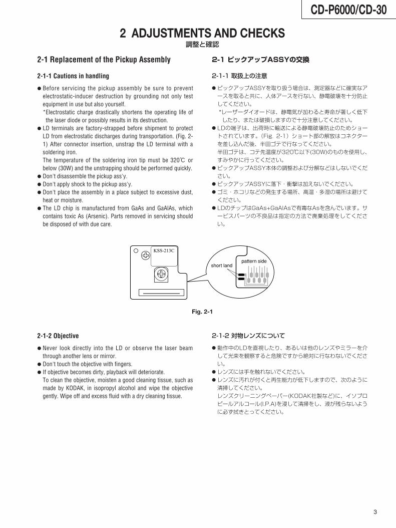
2-1 Replacement of the Pickup Assembly
2-1-1 Cautions in handling
● Before servicing the pickup assembly be sure to preventelectrostatic-inducer destruction by grounding not only testequipment in use but also yourself.*Electrostatic charge drastically shortens the operating life of
the laser diode or possibly results in its destruction.● LD terminals are factory-strapped before shipment to protect
LD from electrostatic discharges during transportation. (Fig. 2-1) After connector insertion, unstrap the LD terminal with asoldering iron.The temperature of the soldering iron tip must be 320℃ orbelow (30W) and the unstrapping should be performed quickly.
● Don't disassemble the pickup ass'y.● Don't apply shock to the pickup ass'y.● Don't place the assembly in a place subject to excessive dust,
heat or moisture.● The LD chip is manufactured from GaAs and GaAlAs, which
contains toxic As (Arsenic). Parts removed in servicing shouldbe disposed of with due care.
2-1-2 Objective
● Never look directly into the LD or observe the laser beamthrough another lens or mirror.
● Don't touch the objective with fingers.● If objective becomes dirty, playback will deteriorate.
To clean the objective, moisten a good cleaning tissue, such asmade by KODAK, in isopropyl alcohol and wipe the objectivegently. Wipe off and excess fluid with a dry cleaning tissue.
2-1 ピックアップASSYの交換
2-1-1 取扱上の注意
● ピックアップASSYを取り扱う場合は、測定器などに確実なアースを取ると共に、人体アースを行ない、静電破壊を十分防止してください。*レーザーダイオードは、静電気が加わると寿命が著しく低下したり、または破損しますので十分注意してください。
● LDの端子は、出荷時に輸送による静電破壊防止のためショートされています。(Fig. 2-1)ショート部の解放はコネクターを差し込んだ後、半田ゴテで行なってください。半田ゴテは、コテ先温度が320℃以下(30W)のものを使用し、すみやかに行ってください。
●ピックアップASSY本体の調整および分解などはしないでください。
●ピックアップASSYに落下・衝撃は加えないでください。●ゴミ・ホコリなどの発生する場所、高温・多湿の場所は避けてください。
● LDのチップはGaAs+GaAlAsで有毒なAsを含んでいます。サービスパーツの不良品は指定の方法で廃棄処理をしてください。
2-1-2 対物レンズについて
● 動作中のLDを直視したり、あるいは他のレンズやミラーを介して光束を観察すると危険ですから絶対に行なわないでください。
●レンズには手を触れないでください。●レンズに汚れが付くと再生能力が低下しますので、次のように清掃してください。レンズクリーニングペーパー(KODAK社製など)に、イソプロピールアルコール(I.P.A)を浸して清掃をし、液が残らないように必ず拭きとってください。
KSS-213C
short landpattern side
Fig. 2-1

4
CD-P6000/CD-30
2-2 Audio Check
2-2-1 Output level check
1. Connect the AC voltmeter to the LINE OUT.2. Play the track 2 (1kHz, 0dB) of the MCD-111, and check the
output level.Specification: 2.0±0.5Vrms (50kΩ load)
2-2-2 PHONES level check
1. Connect the AC voltmeter to the PHONES.2. Play the track 2 (1kHz, 0dB) of the MCD-111, and check the
output level.Specification: 1.0±0.3Vrms (PHONES VR: MAX, 32Ω load)
2-2-3 Distortion check
1. Connect the distortion meter to the LINE OUT.2. Play the track 2 (1kHz, 0dB) of the MCD-111, and check the
distortion.Specification: 0.01% or less (PITCH CONTROL OFF, 20kHz LPF IN)
0.03% or less (PITCH CONTROL ON, 20kHz LPF IN)
2-2-4 Frequency response check
1. Play the track 3-6 (20Hz – 20kHz, 0dB) of the MCD-111, andcheck that output level are within the specified values withrespect to the 1kHz reference level.Specification: within ±0.5dB
2-2-5 S/N check
1. Play the track 7 (non-signal) of the MCD-111, and check thatnoise level are within the specified values with respect to the1kHz reference level.Specification: 96dB or more (A-WEIGHT)
2-2-6 Channel separation check
1. Play the track 8 (L:1kHz / R:non-signal) of the MCD-111, andcheck the leakage from Lch to Rch.
2. In the same way, play the track 10 (R:1kHz / L:non-signal) ofthe MCD-111, and check the leakage from Rch to Lch.Specification: 85dB or more (A-WEIGHT)
2-2-7 Emphasis effect
1. Play the track 13 (16kHz) of the MCD-111, and check thatoutput level are within the specified values with respect to the1kHz reference level.Specification: -20±0.5dB
2-2 オーディオ系の確認
2-2-1 出力レベルチェック
1.LINE OUT端子にACボルトメーターを接続する。2.MCD-111の2曲目(1kHz, 0dB)を再生し、出力レベルを確認する。規格: 2.0±0.5Vrms(50kΩ負荷)
2-2-2 PHONESレベルチェック
1.PHONES端子にACボルトメーターを接続する。2.MCD-111の2曲目(1kHz, 0dB)を再生し、出力レベルを確認する。規格: 1.0±0.3Vrms(PHONES VR: MAX, 32Ω負荷)
2-2-3 歪率チェック
1.LINE OUT端子に歪率計を接続する。2.MCD-111の2曲目(1kHz, 0dB)を再生し、歪率を確認する。規格: 0.01%以下(PITCH CONTROL OFF, 20kHz LPF IN)
0.03%以下(PITCH CONTROL ON, 20kHz LPF IN)
2-2-4 周波数特性チェック
1.MCD-111の3~6曲目(20Hz~20kHz, 0dB)を再生し、基準レベル(1kHz, 0dB)に対し規格内にあることを確認する。規格: ±0.5dB以内
2-2-5 S/Nチェック
1.MCD-111の7曲目(無信号)を再生し、ノイズレベルが基準レベルに対し規格内であることを確認する。規格: 96dB以上(A-WEIGHT)
2-2-6 チャンネルセパレーションチェック
1.MCD-111の8曲目(L:1kHz / R: 無信号)を再生し、Rchへの漏れを確認する。
2.同様に10曲目(R:1kHz / L: 無信号)を再生し、Lchへの漏れを確認する。規格: 85dB以上(A-WEIGHT)
2-2-7 エンファシス効果
1.MCD-111の13曲目(16kHz)を再生し、出力レベルが基準レベルに対し規格内であることを確認する。規格: -20±0.5dB
5
CD-P6000/CD-30
NOTES
● PC boards shown are viewed from parts side.● Parts marked with * require longer delivery time.● The parts with no reference number or no parts number in the
exploded views are not supplied.● As regards the resistors and capacitors, refer to the circuit diagrams
contained in this manual.●£ Parts marked with this sign are safety critical components. They
must be replaced with identical components - refer to the appropriateparts list and ensure exact replacement.
● Parts of [ ] mark can be used only with the version designated.[J]:CD-P6000 JAPAN [E]:CD-P6000 EUROPE [TOA]:CD-30
注 意
● プリント基板図は部品面を示しています。● *印の部品は納期が若干かかります。あらかじめご了承ください。
●分解図に部番のない部品および品番のない部品は供給できません。
●標準の抵抗、コンデンサーは省略してあります。回路図を参照してください。
●£印は安全重要部品です。交換する時は必ず指定の部品を使用してください。
●仕向先[J]:CD-P6000 JAPAN [E]:CD-P6000 EUROPE [TOA]:CD-30
PARTS LIST SECTION
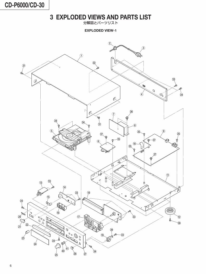
3 EXPLODED VIEWS AND PARTS LIST
EXPLODED VIEW-1
6
分解図とパーツリスト
CD-P6000/CD-30
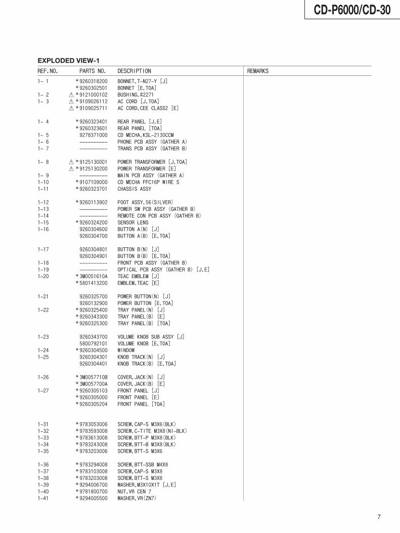
EXPLODED VIEW-1
REF.NO. PARTS NO. DESCRIPTION REMARKS
1- 1 * 9260318200 BONNET,T-N27-Y [J] * 9260302501 BONNET [E,TOA]
1- 2 £ * 9121000102 BUSHING,#2271 1- 3 £ * 9109026112 AC CORD [J,TOA]
£ * 9109025711 AC CORD,CEE CLASS2 [E]
1- 4 * 9260323401 REAR PANEL [J,E] * 9260323601 REAR PANEL [TOA]
1- 5 9278371000 CD MECHA,KSL-2130CCM 1- 6 ---------- PHONE PCB ASSY (GATHER A) 1- 7 ---------- TRANS PCB ASSY (GATHER B)
1- 8 £ * 9125130001 POWER TRANSFORMER [J,TOA] £ * 9125130200 POWER TRANSFORMER [E]
1- 9 ---------- MAIN PCB ASSY (GATHER A) 1-10 * 9107109000 CD MECHA FFC16P WIRE S 1-11 * 9260323701 CHASSIS ASSY
1-12 * 9260113902 FOOT ASSY,56(SILVER) 1-13 ---------- POWER SW PCB ASSY (GATHER B) 1-14 ---------- REMOTE CON PCB ASSY (GATHER B) 1-15 * 9260324200 SENSOR LENS 1-16 9260304600 BUTTON A(N) [J]
9260304700 BUTTON A(B) [E,TOA]
1-17 9260304801 BUTTON B(N) [J] 9260304901 BUTTON B(B) [E,TOA]
1-18 ---------- FRONT PCB ASSY (GATHER B) 1-19 ---------- OPTICAL PCB ASSY (GATHER B) [J,E]1-20 * 3M0051610A TEAC EMBLEM [J]
* 5801413200 EMBLEM,TEAC [E]
1-21 9260325700 POWER BUTTON(N) [J] 9260132900 POWER BUTTON [E,TOA]
1-22 * 9260325400 TRAY PANEL(N) [J] * 9260343300 TRAY PANEL(B) [E] * 9260325300 TRAY PANEL(B) [TOA]
1-23 9260343700 VOLUME KNOB SUB ASSY [J] 5800792101 VOLUME KNOB [E,TOA]
1-24 * 9260304500 WINDOW 1-25 9260304301 KNOB TRACK(N) [J]
9260304401 KNOB TRACK(B) [E,TOA]
1-26 * 3M0057710B COVER,JACK(N) [J] * 3M0057700A COVER,JACK(B) [E]
1-27 * 9260305103 FRONT PANEL [J] * 9260305000 FRONT PANEL [E] * 9260305204 FRONT PANEL [TOA]
1-31 * 9783053006 SCREW,CAP-S M3X6(BLK) 1-32 * 9783593008 SCREW,C-TITE M3X8(NI-BLK) 1-33 * 9783613008 SCREW,BTT-P M3X8(BLK) 1-34 * 9783243008 SCREW,BTT-B M3X8(BLK) 1-35 * 9783203006 SCREW,BTT-S M3X6
1-36 * 9783294008 SCREW,BTT-SSB M4X8 1-37 * 9783103008 SCREW,CAP-S M3X8 1-38 * 9783203008 SCREW,BTT-S M3X8 1-39 * 9294006700 WASHER,M3X10X1T [J,E] 1-40 * 9781800700 NUT,VR CEN 7 1-41 * 9294005500 WASHER,VR(ZN7)
7
CD-P6000/CD-30

CD-P6000/CD-30
EXPLODED VIEW-2
8
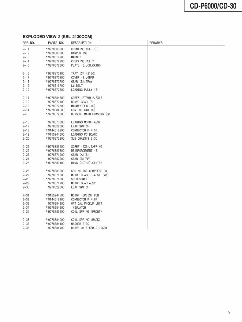
CD-P6000/CD-30
EXPLODED VIEW-2 (KSL-2130CCM)
REF.NO. PARTS NO. DESCRIPTION REMARKS
2- 1 * 9278383600 CHUNKING YOKE (S) 2- 2 * 9278383800 DAMPER (S) 2- 3 * 9278316900 MAGNET 2- 4 * 9278372900 CHUCKING PULLY 2- 5 * 9278372800 PLATE (S),CHUCKING
2- 6 * 9278372100 TRAY (C) (2130) 2- 7 * 9278372300 COVER (S),GEAR 2- 8 * 9278372700 GEAR (S),TRAY 2- 9 9278318700 LM BELT 2-10 * 9278372600 LOADING PULLY (S)
2-11 * 9278384500 SCREW,+PTPWH 2.6X16 2-12 9278372400 DRIVE GEAR (S) 2-13 9278372500 MIDWAY GEAR (S) 2-14 * 9278384600 CONTROL CAM (S) 2-15 * 9278372000 OUTSERT MAIN CHASSIS (S)
2-16 9278373000 LOADING MOTOR ASSY 2-17 9278322000 LEAF SWITCH 2-18 * 9144516200 CONNECTOR PIN 5P 2-19 * 9155244600 LOADING PC BOARD 2-20 * 9278372200 SUB CHASSIS 2130
2-21 * 9278383200 SCREW (2X5),TAPPING 2-22 * 9278383300 REINFORCEMENT (S) 2-23 9278371900 GEAR (A)(S) 2-24 9278382900 GEAR (B)(RP) 2-25 * 9278383100 RING (LO)(S),CENTER
2-26 * 9278383000 SPRING (S),COMPRESSION 2-27 9278371600 MOTOR CHASSIS ASSY (MB) 2-28 * 9278371800 SLED SHAFT 2-29 9278371700 MOTOR GEAR ASSY 2-30 9278322000 LEAF SWITCH
2-31 * 9155244500 MOTOR (6P)(S) PCB 2-32 * 9144516100 CONNECTOR PIN 6P 2-33 9278384900 OPTICAL PICKUP UNIT 2-34 * 9278384300 INSULATOR 2-35 * 9278383900 COIL SPRING (FRONT)
2-36 * 9278384000 COIL SPRING (BACK) 2-37 * 9278384100 WASHER 2130 2-38 9278384400 DRIVE UNIT,KSM-2130CCM
9
CD-P6000/CD-30
10
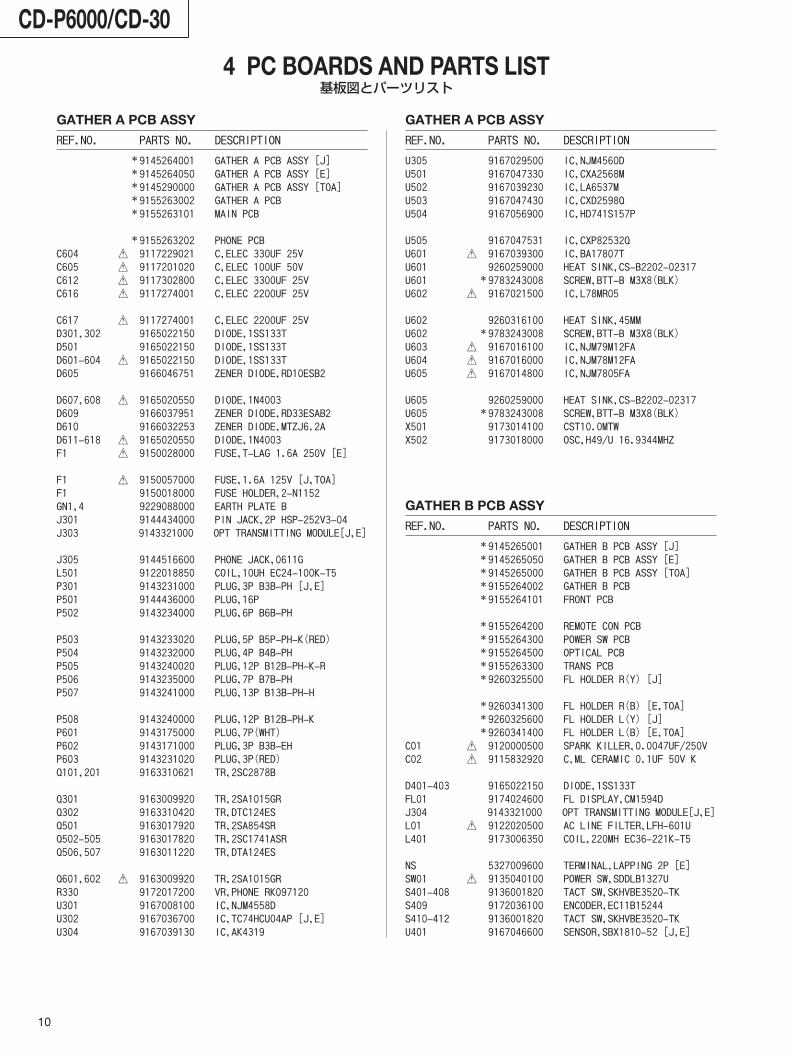
GATHER A PCB ASSY
REF.NO. PARTS NO. DESCRIPTION
* 9145264001 GATHER A PCB ASSY [J] * 9145264050 GATHER A PCB ASSY [E] * 9145290000 GATHER A PCB ASSY [TOA] * 9155263002 GATHER A PCB * 9155263101 MAIN PCB
* 9155263202 PHONE PCB C604 £ 9117229021 C,ELEC 330UF 25V C605 £ 9117201020 C,ELEC 100UF 50V C612 £ 9117302800 C,ELEC 3300UF 25V C616 £ 9117274001 C,ELEC 2200UF 25V
C617 £ 9117274001 C,ELEC 2200UF 25V D301,302 9165022150 DIODE,1SS133T D501 9165022150 DIODE,1SS133T D601-604 £ 9165022150 DIODE,1SS133T D605 9166046751 ZENER DIODE,RD10ESB2
D607,608 £ 9165020550 DIODE,1N4003 D609 9166037951 ZENER DIODE,RD33ESAB2 D610 9166032253 ZENER DIODE,MTZJ6.2A D611-618 £ 9165020550 DIODE,1N4003 F1 £ 9150028000 FUSE,T-LAG 1.6A 250V [E]
F1 £ 9150057000 FUSE,1.6A 125V [J,TOA] F1 9150018000 FUSE HOLDER,2-N1152 GN1,4 9229088000 EARTH PLATE B J301 9144434000 PIN JACK,2P HSP-252V3-04 J303 9143321000 OPT TRANSMITTING MODULE[J,E]
J305 9144516600 PHONE JACK,0611G L501 9122018850 COIL,10UH EC24-100K-T5 P301 9143231000 PLUG,3P B3B-PH [J,E] P501 9144436000 PLUG,16P P502 9143234000 PLUG,6P B6B-PH
P503 9143233020 PLUG,5P B5P-PH-K(RED) P504 9143232000 PLUG,4P B4B-PH P505 9143240020 PLUG,12P B12B-PH-K-R P506 9143235000 PLUG,7P B7B-PH P507 9143241000 PLUG,13P B13B-PH-H
P508 9143240000 PLUG,12P B12B-PH-K P601 9143175000 PLUG,7P(WHT) P602 9143171000 PLUG,3P B3B-EH P603 9143231020 PLUG,3P(RED) Q101,201 9163310621 TR,2SC2878B
Q301 9163009920 TR,2SA1015GR Q302 9163310420 TR,DTC124ES Q501 9163017920 TR,2SA854SR Q502-505 9163017820 TR,2SC1741ASR Q506,507 9163011220 TR,DTA124ES
Q601,602 £ 9163009920 TR,2SA1015GR R330 9172017200 VR,PHONE RK097120 U301 9167008100 IC,NJM4558D U302 9167036700 IC,TC74HCU04AP [J,E] U304 9167039130 IC,AK4319
GATHER A PCB ASSY
REF.NO. PARTS NO. DESCRIPTION
U305 9167029500 IC,NJM4560D U501 9167047330 IC,CXA2568M U502 9167039230 IC,LA6537M U503 9167047430 IC,CXD2598Q U504 9167056900 IC,HD741S157P
U505 9167047531 IC,CXP82532Q U601 £ 9167039300 IC,BA17807T U601 9260259000 HEAT SINK,CS-B2202-02317 U601 * 9783243008 SCREW,BTT-B M3X8(BLK) U602 £ 9167021500 IC,L78MR05
U602 9260316100 HEAT SINK,45MM U602 * 9783243008 SCREW,BTT-B M3X8(BLK) U603 £ 9167016100 IC,NJM79M12FA U604 £ 9167016000 IC,NJM78M12FA U605 £ 9167014800 IC,NJM7805FA
U605 9260259000 HEAT SINK,CS-B2202-02317 U605 * 9783243008 SCREW,BTT-B M3X8(BLK) X501 9173014100 CST10.0MTW X502 9173018000 OSC,H49/U 16.9344MHZ
GATHER B PCB ASSY
REF.NO. PARTS NO. DESCRIPTION
* 9145265001 GATHER B PCB ASSY [J] * 9145265050 GATHER B PCB ASSY [E] * 9145265000 GATHER B PCB ASSY [TOA] * 9155264002 GATHER B PCB * 9155264101 FRONT PCB
* 9155264200 REMOTE CON PCB * 9155264300 POWER SW PCB * 9155264500 OPTICAL PCB * 9155263300 TRANS PCB * 9260325500 FL HOLDER R(Y) [J]
* 9260341300 FL HOLDER R(B) [E,TOA] * 9260325600 FL HOLDER L(Y) [J] * 9260341400 FL HOLDER L(B) [E,TOA]
C01 £ 9120000500 SPARK KILLER,0.0047UF/250VC02 £ 9115832920 C,ML CERAMIC 0.1UF 50V K
D401-403 9165022150 DIODE,1SS133T FL01 9174024600 FL DISPLAY,CM1594D J304 9143321000 OPT TRANSMITTING MODULE[J,E]L01 £ 9122020500 AC LINE FILTER,LFH-601U L401 9173006350 COIL,220MH EC36-221K-T5
NS 5327009600 TERMINAL,LAPPING 2P [E] SW01 £ 9135040100 POWER SW,SDDLB1327U S401-408 9136001820 TACT SW,SKHVBE3520-TK S409 9172036100 ENCODER,EC11B15244 S410-412 9136001820 TACT SW,SKHVBE3520-TK U401 9167046600 SENSOR,SBX1810-52 [J,E]
4 PC BOARDS AND PARTS LIST基板図とパーツリスト

11
MAIN PCB
CD-P6000/CD-30

12
POWER SW PCBREMOTE CON PCB OPT PCB
TRANS PCBPHONE PCB
FRONT PCB
CD-P6000/CD-30

CD-P6000/CD-30
13
5 INCLUDED ACCESSORIES付属品
INCLUDED ACCESSORIES (CD-P6000)
REF.NO. PARTS NO. DESCRIPTION
* 9101417301 OWNER'S MANUAL,JAPANESE [J]* 9101418400 OWNER'S MANUAL,MULTI [E] * 9151003300 REMOTE CONTROL UNIT,RC-728* 5347016500 BATTERY,UM-4 * 9109027111 IN-OUTPUT CORD
INCLUDED ACCESSORIES (CD-30)
REF.NO. PARTS NO. DESCRIPTION
* 9101417902 OWNER'S MANUAL,JAPANESE * 9109027111 IN-OUTPUT CORD * 9260324000 ANGLE R * 9260324100 ANGLE L
* 9260220700 SCREW,RACK BIND 5X12 FC * 9294006200 WASHER,5.2X10.5X1.0T * 9783053012 SCREW,CAP-S M3X12(BLK) * 9294209100 WASHER,FIBER 7.3X3.2X0.5T

CD-P6000/CD-30
14
6 BLOCK DIAGRAMブロックダイアグラム
TO
PT
CL
OU
T S
WIN
SW
TR
AY
MO
TO
R
A CB D E F
LD PD
PIC
KU
P
FC
S+
FC
S-
TR
K+
TR
K-
E F LD PD
LIM
IT S
W
SLE
D+
SLE
D-
SP
IND
LE+
SP
IND
LE-
SE
RV
OM
OT
OR
CD
ME
CH
A
SE
RV
OD
RIV
ERLD
_ON
FE
TE
TE
FE SS
TP
DS
PC
XD
2598
Q
FF
DR
FR
DR
TF
DR
TR
DR
SF
DR
SR
DR
MD
P
DO
UT
SC
OR
SQ
SO
SQ
CK
DA
TA
XLA
TC
LOK
SE
NS
FO
KLO
CK
SIO
1
SIO
0 MIC
OM
CX
P82
532
KE
YM
AT
RIX
FL
DIS
PLA
Y
RF
_AM
PC
XA
2568
M
A B C DR
FR
FLR
CK
V16
M
PC
MD
BC
KE
MP
HB
LCK
EM
PH
SD
AT
ALR
CK
XT
IDA
CA
K43
19
++
AO
UT
L
AO
UT
R
L C
H
R C
H
LIN
E O
UT
2 31
GN
1G
ND
(CD
-P60
00 o
nly) D
IGIT
AL
OU
T(F
RO
NT
)
DIG
ITA
L O
UT
(RE
AR
)
CD-P6000/CD-30
15
Memo
PRINTED IN JAPAN 0300SK 0.2 S-0014
CCDD--PP66000000//CCDD--3300
TEAC CORPORATION 3-7-3, Nakacho, Musashino-shi, Tokyo 180-8550, Japan Phone: (0422) 52-5081
TEAC AMERICA, INC. 7733 Telegraph Road, Montebello, California 90640 Phone: (213) 726-0303
TEAC CANADA LTD. 5939 Wallace Street, Mississauga, Ontario L4Z 1Z8, Canada Phone: 905-890-8008
TEAC MEXICO, S.A. De C.V Privada De Corina, No.18, Colonia Del Carrmen Coyoacon, Mexico DF 04100 Phone: 5-658-1943
TEAC UK LIMITED 5 Marlin House, Marlins Meadow, The Croxley Centre, Watford, Herts. WD1 8YA, U.K. Phone: 01923-819699
TEAC DEUTSCHLAND GmbH Bahnstrasse 12, 65205 Wiesbaden-Erbenheim, Germany Phone: 0611-71580
TEAC FRANCE S. A. 17 Rue Alexis-de-Tocqueville, CE 005 92182 Antony Cedex, France Phone: 01.42.37.01.02
TEAC BELGIUM NV/SA P.A. TEAC Nederland BV, Perkinsbaan 11a, 3439 ND Nieuwegein, Netherlands Phone: 0031-30-6048115
TEAC NEDERLAND BV Perkinsbaan 11a, 3439 ND Nieuwegein, Netherlands Phone: 030-6030229
TEAC AUSTRALIA PTY., LTD. 106 Bay Street, Port Melbourne, Victoria 3207, Australia Phone: (03) 9644-2442A.C.N. 005 408 462
TEAC ITALIANA S.p.A. Via C. Cantù 11, 20092 Cinisello Balsamo, Milano, Italy Phone: 02-66010500
ティアック株式会社 営業部 ¿ (0422)52-5073 〒180-8550 東京都武蔵野市中町3 - 7 - 3
技術的なお問い合わせ AV技術相談室 ¿ (0422)36-2210 〒180-8550 東京都武蔵野市中町3 - 7 - 3
アフター・サービスに関する 札 幌 営 業 所 ¿ (011)521-4101(代) 〒064-0807 札幌市中央区南7条西2 - 2 くぼたビルお問い合わせ 仙 台 営 業 所 ¿ (022)218-0007(代) 〒981-3135 仙台市泉区八乙女中央3 - 2 - 30 リバーサイドヒル及川
新潟サービス ¿ (025)245-0103 〒950-0865 新潟県新潟市本馬越1 - 4 - 11 黒井ハイツ大宮サービス ¿ (048)642-4551 〒331-0052 大宮市三橋2 - 846多摩サービス ¿ (0422)52-5102 〒180-8550 東京都武蔵野市中町3 - 7 - 3東京サービス ¿ (03)3592-1827 〒100-0014 東京都千代田区永田町2 - 10 - 7 星ガ岡会館千葉サービス ¿ (043)255-1281 〒260-0042 千葉市中央区椿森1 - 21 - 13 清水ビル神奈川サービス ¿ (042)746-6850 〒228-0803 相模原市相模大野7-14-9 グリーンシティビル静岡サービス ¿ (054)238-2431 〒422-8034 静岡市高松1 - 12 - 1 寿道ハイツ105号名古屋営業所 ¿ (052)702-3100(代) 〒465-0025 名古屋市名東区上社5 - 406京都サービス ¿ (075)871-8730 〒616-8224 京都市右京区常盤窪町19 西垣ビル大 阪 営 業 所 ¿ (06)6384-5201(代) 〒564-0062 吹田市垂水町3 - 34 - 10兵庫サービス ¿ (0727)55-1002 〒666-0004 兵庫県川西市萩原1 - 11 - 29岡山サービス ¿ (0862)25-8601 〒700-0945 岡山市新保1155 - 1広 島 営 業 所 ¿ (082)294-4751(代) 〒730-0846 広島市中区西川口町13 - 19福 岡 営 業 所 ¿ (092)431-5781(代) 〒812-0008 福岡市博多区東光2 - 2 - 24福岡サービス ¿ (092)957-2050 〒811-2107 福岡県糟屋郡宇美町とびたけ3 - 7 - 12
6 74 52 31
E
D
C
B
A
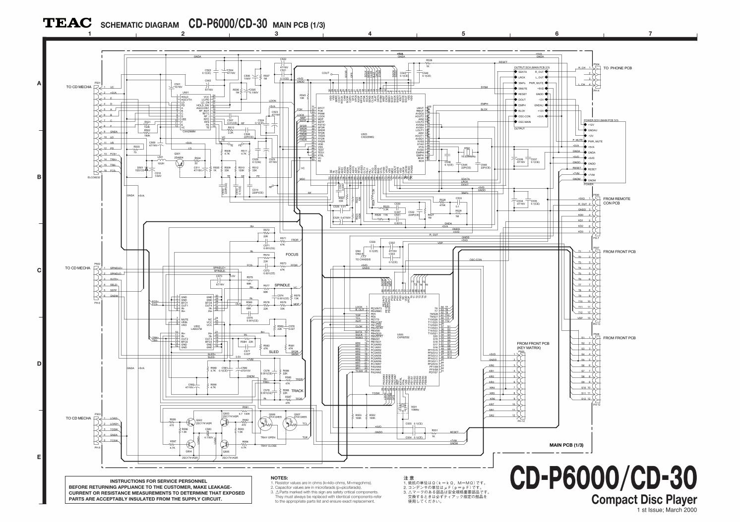
SCHEMATIC DIAGRAM CD-P6000/CD-30 MAIN PCB (1/3)
Compact Disc Player1 st Issue; March 2000
INSTRUCTIONS FOR SERVICE PERSONNELBEFORE RETURNING APPLIANCE TO THE CUSTOMER, MAKE LEAKAGE-CURRENT OR RESISTANCE MEASUREMENTS TO DETERMINE THAT EXPOSEDPARTS ARE ACCEPTABLY INSULATED FROM THE SUPPLY CIRCUIT.
KD1
KD2
KD3
3.5V
OUT
SLED
SPINDLE
3.5V
TRACK
FOCUS
TRAY OPEN
TRAY CLOSE
TO PHONE PCB
FROM REMOTECON PCB
FROM FRONT PCB
FROM FRONT PCB
TO CD MECHA
TO CD MECHA
TO CD MECHA
KD0
FROM FRONT PCB(KEY MATRIX)
TO CHASSIS
POWER.SCH (MAIN PCB 3/3)
POWER
GNDM
+7VM
+12V
-12V
GNDAU
PWR_MUTE
+5VA
GNDA
+5VD
GNDD
RESET
OUTPUT.SCH (MAIN PCB 2/3)
OUTPUT
PWR_MUTE
R_OUT
L_OUT
384Fs
LRCK
BLCK
DOUT
+5VD
GNDD
-12V
GNDAU
+12V
SDATA
EMPH
RESET
SMUTE
+5VAOSC-CON
OSC-MAIN
LOA
D-
LOAD-
LOAD+
LOA
D+
D
A
B
C
PD
VR
LD
LD
E
F
FRDR
SRDR
MDP
FFDRFE
TRDR
MDP
FRDR
TE
SFDR
TFDR
FFDR
TRDR
SE
SRDR
FE
TFDR
RF
TE
SFDR
GNDA
GNDA
GNDA
GNDAGNDA
GNDA
GNDA
GNDA
GNDA
T10
LOCK
XLAT
S8
T2
T5
S5
S6
T1T7
S1
T10
T3
S9
S3
T9
LDON
T6
T1
SQSO
T12
SQ
SO
KR3
S12
DATA
KR0
KR3 S10
XLA
T
KR1
S12
T12
S10
S4
T4
KR2
T8
S4
T9
KR7
S6
R_OUT
S2
SC
LK
KR6
T8
T11R_OUT
S11
TCSW
KR1
S11
KR2
TCL
SC
OR
DA
TA
SC
OR
S7
KR6
S9
S3
LOCK
CLO
K
TOP
VDP
KR5
T7
KR0
SQ
CK
R_OUT
TOP
KR4
S7
S1
TCL
SC
LK
CLOK
S5
VDP
SQCK
T3
S2
GF
S
S8
KR4
T2
KR5
KR7
T11
T5T6T4
GF
S
LDO
N
TCSW
SR1
SR2
SR1SR2
TOSW
TOSW
RF
MD2
MD
2
SE
NS
SE
NS
FO
K
FOK
VC
VC
VC
VC
SSTP
SSTP
IN+
TRK+
+7VM
SPINDLE-
FCS-
+7VM
+7VM
TRK+
FCS+
GNDM
IN-
SPINDLE+SPINDLE+
IN+
FCS-
TRK+
SLED+
FCS-
TRK-
IN+
GNDM
GNDM
SLED-
IN-
FCS+
SPINDLE-
IN-
SELD-
GNDM
IN-
IN+
SLED+
TRK-
+5VD
GNDD
R_CH
GNDD
+5VD
+5VA
+5VD
RESET
GNDD
+5VA
+5VA
OSC-CON
RESET
+5VA
SY
SM
SYSM
+5VD
+5VD
L_CH
LRCK
BLCK
P_MUTE
GNDD
+5VA
384Fs
GNDD
EMPH
SY
SM
+5VD
GNDD
+5VD
+5VA
+5VA
DOUT
+5VD
GNDD
GNDD
GNDD
RESET
+5VD
SDATA
+5VA +5VA+5VA
P508
PH-12
1
2
3
4
5
6
7
8
9
10
11
12
P503
PH-5
1
2
3
4
5
P501
ELCO6232
1
2
3
4
5
6
7
8
9
10
11
12
13
14
15
16
P506
PH-7
1
2
3
4
5
6
7
U501
CXA2568M
HOLD1
AGCVTH2
LD3
PD4
A5
B6
C7
D8
VEE9
F10
E11
VC12 TE 13FE14RFE 15RFO16RF_I 17RFTC 18RF_BOT19AGCCONT 20HOLD_SW21LD_ON 22LC/PD 23VCC24
U503CXD2598Q
VD
D1
VS
S2
SO
UT
3S
OC
K4
XO
LT5
SQ
SO
6S
QC
K7
SC
SY
8S
BS
O9
EX
CK
10X
RS
T11
SY
SM
12D
AT
A13
XLA
T14
CLO
K15
SE
NS
16S
CLK
17A
TS
K18
WF
CK
19X
UG
F20
XP
CK
21G
FS
22C
2PO
23S
CO
R24
C4M
25W
DC
K26
CO
UT
27M
IRR
28V
SS
29V
DD
30
DFCT31
FOK32
PWMI33
LOCK34
MDP35
SSTP36
FSTIO37
SFDR38
SRDR39
TFDR40
TRDR41
FFDR42
FRDR43
VDD44
VSS45
TEST46
TES147
XTSL48
VC49
FE50
SE
51
TE52
CE
53
RF
DC
54
AD
IO55
AV
SS
56
IGE
N57
AV
DD
058
AS
YO
59
AS
YI
60
RF
AC
61
AV
SS
362
CLT
V63
FIL
O64
FIL
I65
PC
O66
AV
DD
367
BIA
S68
VC
TL
69
V16
M70
VP
CO
71
VS
S72
MD
273
DO
UT
74
AS
YE
75
VD
D76
LRC
K77
LRC
KI
78
PC
MD
79
PC
MD
I80
BCK81BCKI 82EMPH 83EMPHI84XVDD 85XTAI86XTAO 87XVSS 88AVDD189AOUT1 90AIN191LOUT1 92AVSS1 93AVSS294LOUT2 95AIN296AOUT2 97AVDD2 98RMUT99LMUT 100
P507
PH-13
1
2
3
4
5
6
7
8
9
10
11
12
13
P505
PH-12
1
2
3
4
5
6
7
8
9
10
11
12
U505CXP82532
PE4/RMC2
PE64
PB0/CINT6
PB2/SCK08
PB4/SO010
PB6/SI112
PC0/KR014
PC2/KR216
PC4/KR418
PC6/KR620
PA0/AN022
PA2/AN224
PA
4/A
N4
26
PA
6/A
N6
28
RS
T30
XTA
L32
PD
0/S
034
PD
2/S
236
PD
4/S
438
PD
6/S
640
PD7/S7 41
PF1/S9 43
PF3/S1145
PF5/S1347
PF7/S15 49
S17 51
S19 53
T15/S2155
T13/S2357
T11/S25 59
T9/S27 61
T7 63
T565
T367
T169
VF
DP
71
NC
73
PG
175
PG
377
PE
1/E
C1/
INT
179
PE3/INT31
PE53
PE7/T05
PB1/CS07
PB3/SI09
PB5/SCK111
PB7/SO113
PC1/KR115
PC3/KR317
PC5/KR519
PC7/KR721
PA1/AN123
PA
3/A
N3
25
PA
5/A
N5
27
PA
7/A
N7
29
EX
TAL
31
VS
S33
PD
1/S
135
PD
3/S
337
PD
5/S
539
PF0/S842
PF2/S10 44
PF4/S12 46
PF6/S14 48
S1650
S1852
S20 54
T14/S22 56
T12/S24 58
T10/S2660
T8/S2862
T6 64
T466
T268
T070
VD
D72
PG
074
PG
276
PE
0/E
C0/
INT
078
PE
2/IN
T2
80
X502
16.9344MHz
R580
68K
R57513K
R579
68K
R584 22K
R58222K
R577
68K
R576
33K
R578
22K
R58347K
R58147K
R58622K
R58822K
R585
47K
R573
47K
R574
22K
R572
22K
R591
4.7 1/4W
R592
470
R5931.5K
R5961.5K
R595
470
R597
4.7K
R502
150K
R503
75
R504
22
R5051K
R5061M
R536
1K
R50933K
R510120K
R5114.7K
R51233K
R5084.7K
R5271M
R526 11K
R5253.3K
R528
470K
R529
1M
R553100K
R552100K
R571
47K
R594
4.7K
R5071M
R513
2.2K
R587
47K
R54510K
R52
210
KR
523
100K
R52133K
R52
43.
3K
R551
1K
C5810.1(CE)
C5750.001(CE)
C5770.027
C5740.001(CE)
C5760.027
C5780.001(CE)
C5790.001(CE)
C5720.001(CE)
C5710.001(CE)
C553
0.1(CE)
C5070.01(CE)
C5440.1(CE)
C521
0.1(CE)
C528 0.01
C5370.1(CE)
C5350.1(CE)
C51
30.
1(C
E)
C514220P(CE)
C532220P(CE)
C530
0.047
C533
0.1
C5240.1(CE)
C5260.1(CE)
C50822P(CE)
C5380.1(CE)
C5030.1(CE)
C52
70.
0047
C54522P(CE)
C54622P(CE)
C51
222
0P(C
E)
C58247/16V
C573
47/16V
C580470/10V
C552
47/16V
C50110/16V
C51147/16V
C5061/50V
C5050.1/50V
C522
47/16V
C53647/16V
C53447/16V
C529 0.47/50V
C50447/16V
C502
47/16V
C52347/16V
C52547/16V
C5101/50V
C50947/16V
Q507DTA124ES
Q506DTA124ES
Q5032SC1741ASR
Q505
2SC1741ASR
Q5022SC1741ASR
Q504
2SC1741ASR
C583
4.7/50V
R5894.7K
R5904.7K
D5011SS133
L501
10UH
Q501
2SA854
TE FE
RF
COUT
R501
150K
P502
PH-6
1
2
3
4
5
6
U502LA6537M
GND1
GND2
BFO13
OUT14
IN-5
IN+6
MUTE7
VRIN8
VRO9
IN+10
IN-11
OUT212
BFO213
GND14
GND15
GND 30
GND29
GND16GND 17BFO318OUT3 19IN- 20IN+21
BFO4 28
OUT427
IN- 26
IN+ 25
VCC 22VCC 23NC24
C531
0.0015
C5430.1(CE)
C556
0.1(CE)GN4GND-8
C555 0.1(CE)
X50110MHz
C554 0.1(CE)
P504
PH-4
1
2
3
4
MAIN PCB (1/3)
CCDD--PP66000000//CCDD--3300NOTES:1. Resistor values are in ohms (k=kilo-ohms, M=megohms).2. Capacitor values are in microfarads (p=picofarads).3. £Parts marked with this sign are safety critical components.
They must always be replaced with identical components-refer to the appropriate parts list and ensure exact replacement.
注意1. 抵抗の単位はΩ(k=kΩ,M=MΩ)です。2. コンデンサの単位はμF(p=pF)です。3. £マークのある部品は安全規格重要部品です。交換するときは必ずティアック指定の部品を使用してください。
6 74 52 31
E
D
C
B
A
SCHEMATIC DIAGRAM
Compact Disc Player1 st Issue; March 2000
INSTRUCTIONS FOR SERVICE PERSONNELBEFORE RETURNING APPLIANCE TO THE CUSTOMER, MAKE LEAKAGE-CURRENT OR RESISTANCE MEASUREMENTS TO DETERMINE THAT EXPOSEDPARTS ARE ACCEPTABLY INSULATED FROM THE SUPPLY CIRCUIT.
LINE OUT
L
R
14
7
(FRONT PANEL)
DIGITAL OUTPUT(OPTICAL FORMAT)
DIGITAL OUTPUT(OPTICALFORMAT)
(REAR PANEL)
RGND
LGND
L LINEOUT
LGND
RGND
R LINEOUT
(CHASSIS GND)
J303
TOTX178
INPUT3
VCC2
GND1
P301
PH-3
1
2
3
P302
SAN-3
1
2
3
J304
TOTX178
INPUT3
VCC2
GND1
R317
240
C31247/16V
C31647/16V
C31747/16V
C308
47/25V
C309
47/25V
D3021SS133
R202
10K
R206
10K
R11210K
R105
470
R106
10KJ301
HSP-252V3
2
3
1
C3022.2(Chip)
R207100K
U301ANJM4558D
2
31
84
R108
100
R107100K
C30310/16V
R101
10K
Q302DTC124ES
C1060.001(CE)
R10310K
R10410K
C30510/16V
C3042.2(Chip)
C105
47/16VC101470P(CE)
U301BNJM4558D
6
57
R205
470
R208100
R11110K
R201
10K
C3062.2(Chip) C202
180P(CE)
C205
47/16V
Q2012SC2878GR
C204180P(CE)
R20410K
R30110K
Q3012SA1015GR
C102180P(CE)
C104180P(CE)
R102
10K
C30110/16V
R21210K
R3021K
C2060.001(CE)
R20310K
C307
0.01
Q1012SC2878GR
C201470P(CE)
R21110K
U302E
74HCU04
11 10
U302C
74HCU04
5 6
U302D
74HCU04
9 8
R540
220
R546220
R541 220
R544 220
R543 220
R542 220
U304AK4319
DIF
11
DV
DD
2
DV
SS
3
LRC
K4
BIC
K5
SD
AT
A6
PD
-7
XT
I8
XTO
9
CLK
O10
SM
UT
E11
DE
M0
12D
EM
113
CK
S14
TST
15A
OU
TR
-16
AO
UT
R+
17A
OU
TL-
18A
OU
TL+
19V
RE
F20
AV
DD
21A
VS
S22
DZ
F23
DIF
024
R303
10K
U504
74157
SELECT1
1A2
1B3
1Y4
2A5
2B6
2Y7
GND8 3Y 93B 103A114Y 124B134A 14STROBE 15VCC16
D3011SS133
R304100K
R548 220
R547 220
+12V
GNDAU
+5VD
GNDD
-12V
PWR_MUTE
EMPH
L_OUT
DOUT
R_OUT
SMUTE
LRCK
BLCK
SDATA
384Fs
RESET
+5VA
OSC-CON
OSC-MAIN
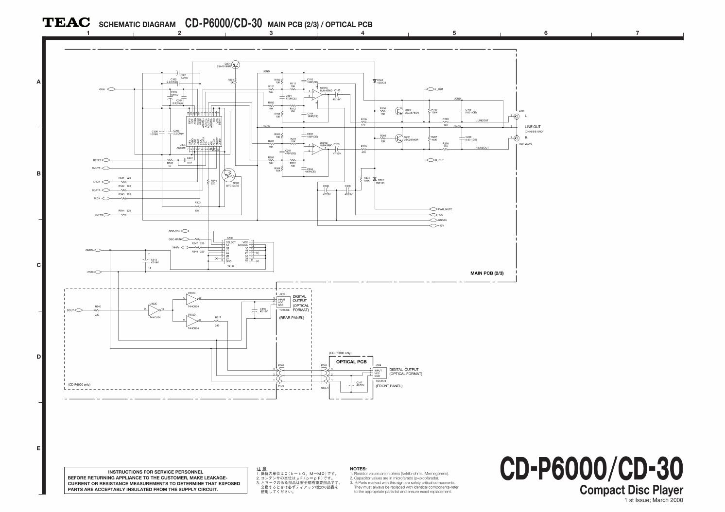
MAIN PCB (2/3)
OPTICAL PCB
(CD-P6000 only)
(CD-P6000 only)
CCDD--PP66000000//CCDD--3300
CD-P6000/CD-30 MAIN PCB (2/3) / OPTICAL PCB
NOTES:1. Resistor values are in ohms (k=kilo-ohms, M=megohms).2. Capacitor values are in microfarads (p=picofarads).3. £Parts marked with this sign are safety critical components.
They must always be replaced with identical components-refer to the appropriate parts list and ensure exact replacement.
注意1. 抵抗の単位はΩ(k=kΩ,M=MΩ)です。2. コンデンサの単位はμF(p=pF)です。3. £マークのある部品は安全規格重要部品です。交換するときは必ずティアック指定の部品を使用してください。
6 74 52 31
E
D
C
B
A
SCHEMATIC DIAGRAM
Compact Disc Player1 st Issue; March 2000
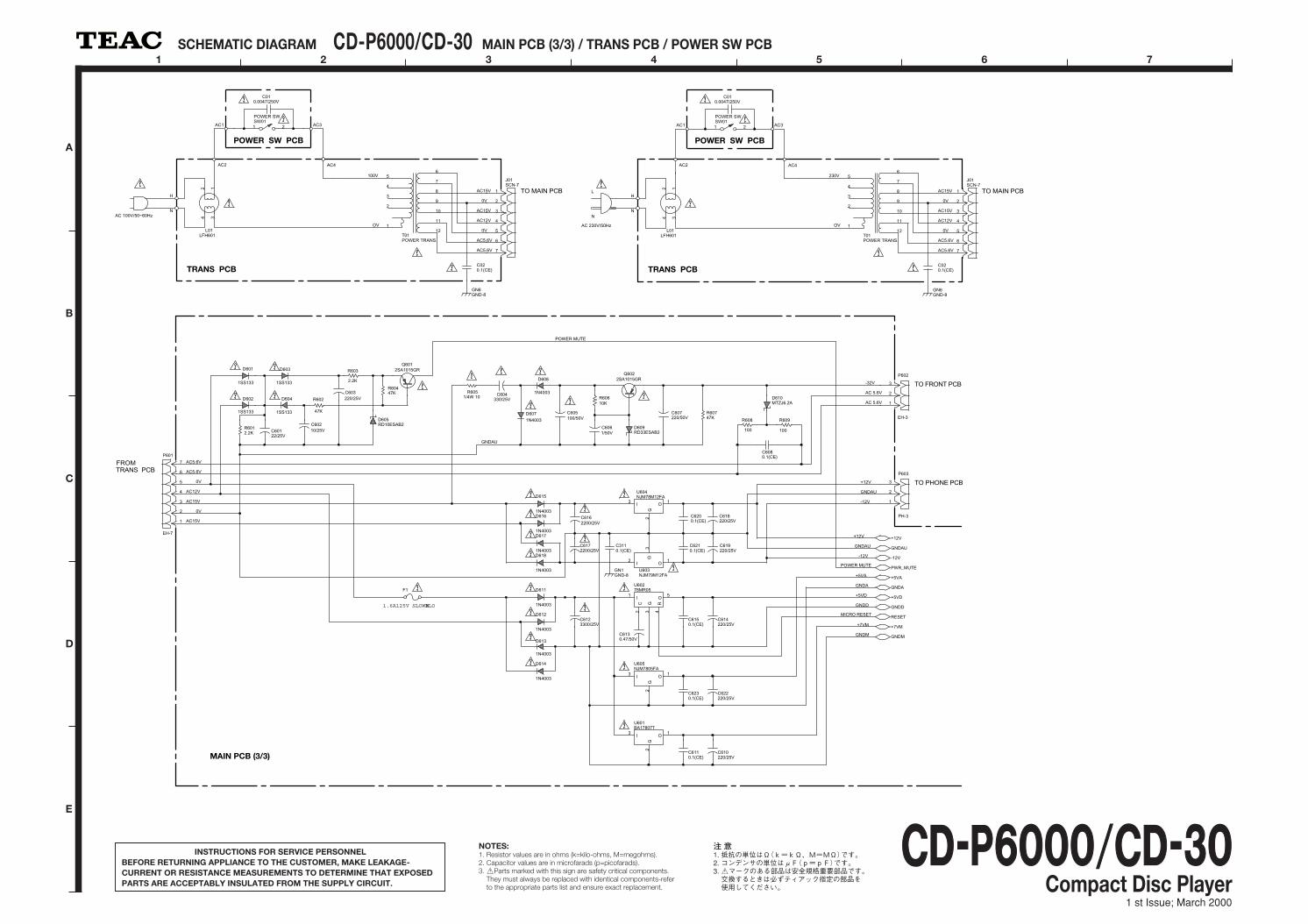
INSTRUCTIONS FOR SERVICE PERSONNELBEFORE RETURNING APPLIANCE TO THE CUSTOMER, MAKE LEAKAGE-CURRENT OR RESISTANCE MEASUREMENTS TO DETERMINE THAT EXPOSEDPARTS ARE ACCEPTABLY INSULATED FROM THE SUPPLY CIRCUIT.
AC 5.6V
AC 5.6V
FROM TRANS PCB
GNDAU
1.6A125V SLOWBLOW
-32V
POWER MUTE
TO FRONT PCB
AC5.6V
POWER MUTE
MICRO RESET
AC5.6V
AC12V
0V
0V
AC15V
AC15V
TO PHONE PCB
+7VM
GNDAU
+12V
GNDD
GNDM
-12V
+5VD
+5VA
GNDA
-12V
GNDAU
+12V
D603
1SS133
D604
1SS133
R602
47K
R603
2.2K
Q6012SA1015GR
R60447K
C6110.1(CE)
P601
EH-7
1
2
3
4
5
6
7
D601
1SS133
D602
1SS133
R6012.2K C601
22/25V
C60210/25V
C603220/25V
D605RD10ESAB2
C610220/25V
F1
D614
1N4003
D613
1N4003
D612
1N4003
D611
1N4003
C6123300/25V
U601BA17807T
I3
O1
G2
C6130.47/50V
C614220/25V
C6150.1(CE)
GN1GND-8
D618
1N4003
D617
1N4003
D616
1N4003
D615
1N4003
U603NJM79M12FA
I2
O1
G3
U604NJM78M12FA
I3 O 1
G2C616
2200/25V
C6172200/25V
C618220/25V
C619220/25V
C6200.1(CE)
C6210.1(CE)
C6080.1(CE)
R608
100
R609
100
D610MTZJ6.2A
R60747K
C607220/50V
D609RD33ESAB2
Q6022SA1015GR
C6061/50V
R60610K
C605100/50V
D608
1N4003
D6071N4003
C604330/25V
R6051/4W 10
U60278MR05
I1
O5
G3
C2
R4
P602
EH-3
1
2
3
C6230.1(CE)
C622220/25V
U605NJM7805FA
I3 O 1
G2
P603
PH-3
1
2
3
C3110.1(CE)
GNDM
+7VM
RESET
GNDD
+5VD
GNDA
+5VA
PWR_MUTE
-12V
GNDAU
+12V
MAIN PCB (3/3)
POWER SW PCB
0V
AC12V
AC15V
AC5.6V
AC15V
0V
TRANS PCB
AC5.6V
H
N
100V
OV
AC 100V/50~60Hz
C010.0047/250V
T01POWER TRANS.
4
3
2
1
8
10
9
12
11
7
65
SW01POWER SW
1 2
AC2
J01SCN-7
1
2
3
4
5
6
7
L01LFH601
2 134
AC1 AC3
AC4
C020.1(CE)
GN6GND-8
TO MAIN PCB0V
AC12V
AC15V
AC5.6V
AC15V
0V
AC5.6V
H
N
230V
OVAC 230V/50Hz
T01POWER TRANS.
4
3
2
1
8
10
9
12
11
7
65
1
2
3
4
5
6
7
L01LFH601
2 134
L
N
TRANS PCB
POWER SW PCB
TO MAIN PCB
J01SCN-7
C020.1(CE)
GN6GND-8
AC4AC2
C010.0047/250V
SW01POWER SW
1 2 AC3AC1
CCDD--PP66000000//CCDD--3300
CD-P6000/CD-30 MAIN PCB (3/3) / TRANS PCB / POWER SW PCB
NOTES:1. Resistor values are in ohms (k=kilo-ohms, M=megohms).2. Capacitor values are in microfarads (p=picofarads).3. £Parts marked with this sign are safety critical components.
They must always be replaced with identical components-refer to the appropriate parts list and ensure exact replacement.
注意1. 抵抗の単位はΩ(k=kΩ,M=MΩ)です。2. コンデンサの単位はμF(p=pF)です。3. £マークのある部品は安全規格重要部品です。交換するときは必ずティアック指定の部品を使用してください。
FRONT PCB
-32V
AC 5.6V
AC 5.6V
FROM MAIN PCB
TO MAIN PCB
PUSH ENTER
TRACK SEARCH
TO MAIN PCB
TO MAIN PCB
REMOTE CON PCB
TO CHASSIS
S11S12 S8 S5
S6T10 T6T8 T4
T5T11T12
T1T7T9T2
T3S10
S9 S4 S3S7 S2
S1
KR
1
KR
3
KR
4
KR
6
KR
7
KR
5
KR
0
KR
2
+5VD
GN
DD
SR
1
SR
2
KS0
KS1
KD1
KD2
KD3
GNDD
R_OUT
KD0
+5VD
S404
PROGRAM
S405
REPEAT
S406
STOP
S407
PLAY
S408
PAUSE
S403
REW SEARCH
S402
FF SEARCH
D402
1SS133
D401
1SS133
R425
100K
R431
100K
R430
100K
R429
100K
R432
100K
R426
100K
R428
100K
R427
100K
S401
OPEN/CLOSE
FL01FLTUBE-CM1594D
F1
1
F1
2
G12
5
G11
6
G10
7
G9
8
G8
9
G7
10
G6
11
G5
12
G4
13
G3
14
G2
15
G1
16
S10
54
S11
55
S12
56
S9
57
S8
58
S4
59
S5
60
S3
61
S7
62
S6
63
S2
64
S1
65
F2
68
F2
69
R416
22K
R413
22K
R420
22K
R414
22K
R417
22K R418
22KR419
22K
R415
22K
R422
22KR423
22K R424
22K
R421
22K
R404
22K
R401
22K
R408
22K
R402
22K
R405
22K R406
22KR407
22K
R403
22K
R410
22KR411
22K R412
22K
R409
22K
P401
DG-3
1
2
3
P402DS-12
123456789101112
S410
PITCH +
S411
PITCH -
S412
PITCH CON.
U401
SBX1810-52
VCC3
OUT 2
GND 1
P405
DS-7
1
2
3
4
5
6
7
P403DS-13
12345678910111213
P404DS-12
123456789101112
D403
1SS133
L401
220UH
1 2
C401100P(CE)
C402100P(CE)
R43410K
R43310K
R435100K
R436100K
R437100K
S409ENCODER
A C B45
C4030.1(CE)
GN5GND-8
HEADPHONEOUTPUT
ROUT
LOUT
FROM MAIN PCB
HEADPHONE PCB
R-CH
L-CH
TO CHASSIS
-12V
+12V
GNDAU
R234
68
R13210K
C234470P(CE)
C134470P(CE)
C3330.1(CE)
U305BNJM4560D
6
57
J3050611G2
31
GN2GND-8
C33247/25V
C33147/25V
U305ANJM4560D
2
31
84
R23210K
R233
27K
R231
1K
R330AVR 20KA
31
2
R330BVR 20KA
46
5
R130100K
R230100K
C233
220P(CE)
C132
10/16V
C232
10/16V
C131
10/16V
C231
10/16V
R131
1K
R133
27K
C133
220P(CE)
R134
68
R135
22K
R235
22K
P305SCN-7
1234567
TO MAIN PCB
(CD-P6000 only)
6 74 52 31
E
D
C
B
A
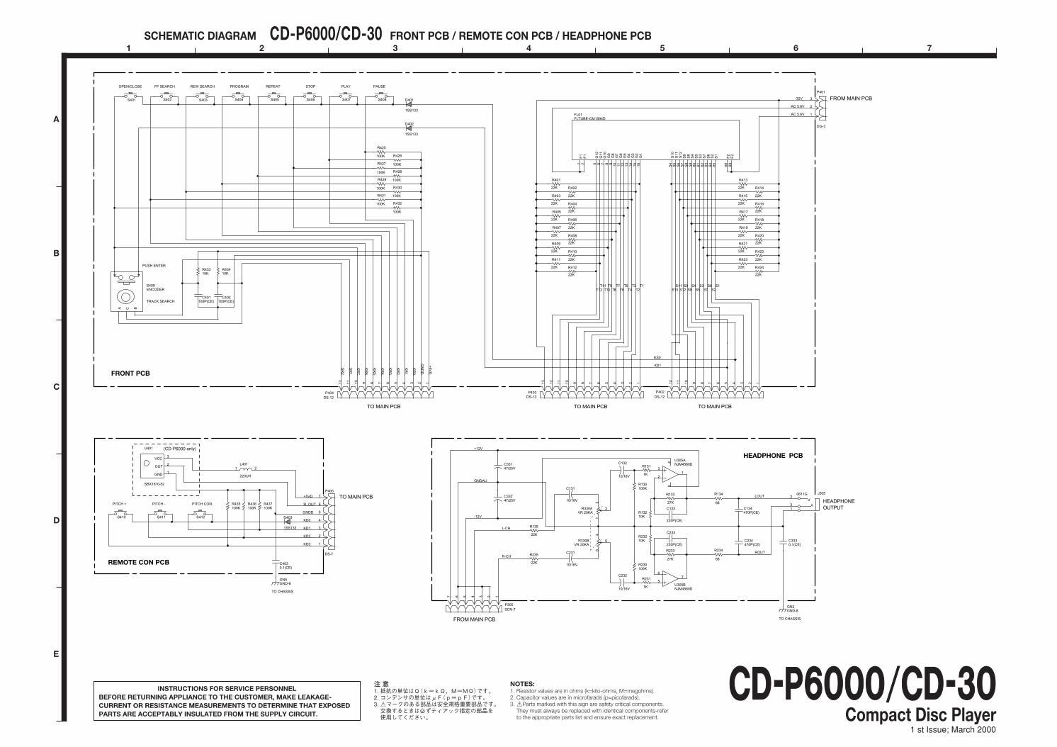
SCHEMATIC DIAGRAM CD-P6000/CD-30 FRONT PCB / REMOTE CON PCB / HEADPHONE PCB
Compact Disc PlayerCCDD--PP66000000//CCDD--3300
1 st Issue; March 2000
INSTRUCTIONS FOR SERVICE PERSONNELBEFORE RETURNING APPLIANCE TO THE CUSTOMER, MAKE LEAKAGE-CURRENT OR RESISTANCE MEASUREMENTS TO DETERMINE THAT EXPOSEDPARTS ARE ACCEPTABLY INSULATED FROM THE SUPPLY CIRCUIT.
NOTES:1. Resistor values are in ohms (k=kilo-ohms, M=megohms).2. Capacitor values are in microfarads (p=picofarads).3. £Parts marked with this sign are safety critical components.
They must always be replaced with identical components-refer to the appropriate parts list and ensure exact replacement.
注意1. 抵抗の単位はΩ(k=kΩ,M=MΩ)です。2. コンデンサの単位はμF(p=pF)です。3. £マークのある部品は安全規格重要部品です。交換するときは必ずティアック指定の部品を使用してください。
Related Documents