TCAD, EDA and IP to Support SOI technologies

Welcome message from author
This document is posted to help you gain knowledge. Please leave a comment to let me know what you think about it! Share it to your friends and learn new things together.
Transcript
TCAD, EDA and IP to Support SOI technologies

Silvaco Overview

• 400+ customers in world wide
•Market Leadership Areas
• # 1 Full FPD Flow
• # 1 Radiation & Reliability
• # 2 Process & Device TCAD
• # 4 Full AMS/Power IC Flow
Leading TCAD, EDA and IP provider
- 3 -

Expanding Worldwide Footprint
Santa Clara(HQ) Shanghai
offices in world wide12
Texas
BostonUK
Austria
France
India
SingaporeTaiwan
Japan
Korea
- 4 -

Mergers are a key part of our Growth Strategy
May
2015
Dec
2015
May
2016
May
2016
Power integrity sign-off market
Advanced variation
aware design
Netlistanalysis & reduction
Enter IP market
Strengthen IP market
Aug
2017
- 5 -

TCAD-to-Signoff
• Silvaco is only one provider
• TCAD
• Spice Modeling
• Custom Design CAD
• Signoff tools
• IP
- 6 -

TCAD-to-Signoff Design Flow
Layout
Spice
Parasitic extraction
Spice modeling
Process
Device
Measured Data
Schematic
Spice
LVS
DRC
TCAD
Parasitic reduction
Modeling Design & Verification
Reliability Analysis
Variation Analysis
Simulation
- 7 -

Vertical Solutions to End-User Market Applications
AMBA
JTAG
Wireless charging,
Lidar, drive train
Multiple form factor in-vehicle display
Device aging, EM/IR/Thermal,
soft errors
Rear camera, IR sensors
High sigma sense & control
PowerPC MCU, CAN-FD Flexible display, LAE
High perf servers & memory
ULP digital blocks
ColdfireMCU
USB
Automotive IoTMobile
- 8 -

TCAD-to-Signoff Vertical Solutions
SOI available
- 9 -

TCAD
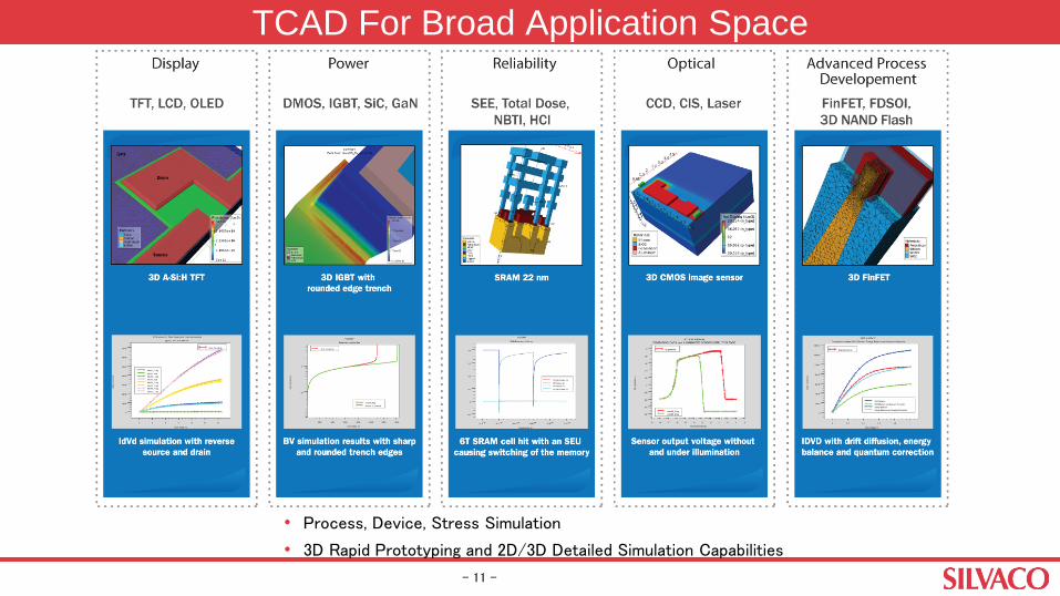
• Process, Device, Stress Simulation
• 3D Rapid Prototyping and 2D/3D Detailed Simulation Capabilities
TCAD For Broad Application Space
- 11 -
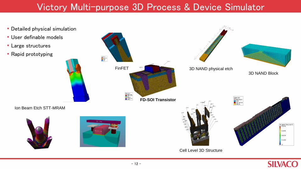
Victory Multi-purpose 3D Process & Device Simulator
• Detailed physical simulation
• User definable models
• Large structures
• Rapid prototyping
FinFET 3D NAND physical etch
FD-SOI Transistor
Cell Level 3D Structure
Ion Beam Etch STT-MRAM
3D NAND Block
- 12 -

• Local oxidation to form silicon islands
• Shallow implant and RTA diffusion process steps
• Physical etching of silicon islands for accurate edge profiles
• Temperature dependent mobility and recombination models
• Oxide interface and bulk charge
• Impact ionization for breakdown and kink effect
• Physical capacitance extraction
• Quantum effects modeling: Schrodinger Approach and Density Gradient Model
• Self heating. Thermal and electrical effects are coupled through self-consistent calculations
• Coupled device simulation within a circuit in MixedMode
• Single event upset
TCAD include SOI specific features:
- 13 -

Fully Depleted: Effect of Back Bias
20nm FDSOI by Victory Process
Effect of Back Bias. Reverse Body Bias (RBB) increases Vth but decreases leakage,Forward Body Bias (FBB) increases Leakage but decreases Vth (making the device faster)
- 14 -

Fully Depleted: Lattice Heating and Quantum Confinement
IV curves simulated by Victory Device showing the impact of Lattice Heating, Quantum Correction and Energy Balance
20nm FDSOI by Victory Process
- 15 -

Partially Depleted: Kink Effect
IV characteristics for long channel device.
Drain IV curves for long channel (left) and short channel (right) SOI devices. Negative conductance due to self-heating at high Vgs is seen in the short channel device. The kink effect is seen more prominently in the long channel device.
IV characteristics for short channel device.
- 16 -

SPICE Portfolio

Supported SOI Compact Models in Silvaco Tools
PDSOI FDSOI UTBB-FDSOI
BSIM-SOIv3.0-3.2 and v4.0-4.5
BSIM-IMGv102.0-102.8
HiSIM_SOIv1.0.0-v1.3.0
HiSIM_SOTBv1.0.0-1.1.0
LETI-SOIv3.0-3.2 and v4.0
LETI-UTSOIv2.1
- 18 -

UTMOST IV - Parameter Extraction & Optimization
90nm FDSOI device characterization using Verilog-A BSIMSOI 4.5 module
- 19 -

SmartSpice and SmartSpice Pro
SmartSpice (red) vsSmartSpice Pro (blue)
Support negative bias condition to
provide accurate and reliable for SOI
- 20 -

• Block to full chip level
• Pure SPICE accuracy for Transistor level
• Early (layout only) IR/EM analysis
Power Integrity and Reliability Analysis
InVar Power
InVar IR
InVar EM
InVar Thermal
Concurrent Power-Voltage-Thermal Analysis
- 21 -

Invar Thermal
- 22 -

Variation Manager Overview
- 23 -
• 3 to 7+
• Fewer Monte Carlo samples
• Strong partner to FDSOI leaders for Memory and Std. Cell libraries
• Improved design margining
• Simulator Agnostic• SmartSpice
• HSPICE, CustomSim-XA
• Spectre, Spectre-RF
• Eldo, Eldo-RF, AFS
• MSIM
• SMASH

• Fast Monte Carlo
• Familiar use method
• 10X+ speedup, brute force MC accuracy
• Statistical corners, Local mismatch
Variation Manager for Analog
- 24 -
FMC
MC
3X 10X

VX validation
Sense Amplifier, FDSOI 28nm:Variation Manager validated on 1M of MC runs
- 25 -
Q-Q Plot (sigma vs performance)Brute Force MC validation
Red: 1M Monte Carlo
Blue: VX
Extremes

FDX 22nm SRAM Bitcell High Sigma shows results up to 8 sigma
- 26 -
Q-Q Plot (sigma vs performance) DOE on Yield estimation
VDD (mV)
NBL 0mV
NBL -100mV
NBL -150mV

Netlist Management Products Overview
- 27 -

• Post layout simulation critical at advanced nodes, but massive impact on simulation time
• Accuracy requirements set by user
• Selective reduction, temperature aware reduction, merge multi-finger devices
Jivaro Advanced Netlist Reduction
- 28 -

Viso:Design Analysis
Belledonne and Viso LPE flows to save time
- 29 -
Belledonne:Netlist Comparison
Design Data
LPE Netlist

Custom Design

OA iPDK Schematic/Layout
• Support OpenAccess D/B
• iPDK compatible
• Support tcl callback in PyCell
- 31 -

Semiconductor IP

Silvaco IP Businesses
• Collaborations with Tier 1 semiconductor companies to unlock valuable IP for licensing to the entire semiconductor industry
IP Commercialization
• Collaborations with specialty IP providers to provide customers differentiated IP solutions
IP Industry Leadership
• Xena is a scalable cloud-based platform for managing IP inside semiconductor and IP companies
IP Management
• IP Fingerprinting and DNA analysis that allows for detection of IP in SoC devicesIP Compliance
- 33 -

Silvaco IP Line up
CAN
CAD FD
MultiCAN
FlexCAN (FD) - New
FlexRay
TriCore Microcontroller
Multiprocessor Link Interface
MicroSecond Channel
Automotive
Interfaces
USB 1.1 Dev
USB 1.1 Host+Dev
USB 2.0 Dev
USB 2.0 Host+Dev
USB 2.0 PHY
USB 1.1 IO
Debug
IEEE 1149.7 cJTAG
Nexus 5001
Processors
ColdFire V1 Core (32-bit)
ColdFire V1 Platform (32-bit)
ColdFire V2 Core (32-bit)
ColdFire V2 Platform(s) (32-bit)
ColdFire V4 Core (32-bit)
ColdFire V4 Platform(s) (32-bit)
Power Architecture e200z0 (32-bit)
Power Architecture e200z1 (32-bit)
Power Architecture e200z3 (32-bit)
Power Architecture e200z6 (32-bit)
CR16 (16-bit)
C166S (16-bit)
M8051EW (8-bit)
HCS08 (8-bit)
AMBA Subsystem
Adv. Audio Interface
I2C
I3C
I2S
USART
GPIO
DMA
Interrupt Controller
SPI
Multi-Function Timer
Multi-Input Wakeup
RAM Controller
Timer & Watchdog
Versatile Timer
Realtime Clock
AHB Backbone
AHB-APB Bridge
- 34 -

#1 Automotive IP Portfolio
Automotive Grade
Embedded Processors
IEEE Debug Standards
- 1149.7
FlexRay Networking
CAN Interfaces
I3C Sensor
Controllers
MultiLink Interface
MicroSecond Channel
- 35 -

I3C Products
Dual-Role Master
Protocol Engine
Host Interface
I3C
APB
CDC
Advanced Slave
Protocol Engine
Host Interface
I3C
APB
CDC
Autonomous Slave
Protocol Engine
I3C
Autonomous
Registers
- 36 -

• ESD and IO Design Experts• Broad Foundry and Process experience
• 1um to 16nm CMOS, SOI, LD-MOS, BCD in Si, GaAs, GaN, SiGe, SoS
• Key Expertise• RF ESD - Low cap, high protection integrated solutions
• Very High Voltage: >10V applications on low voltage 1.8/3.3V CMOS Process
• High Performance SerDes: 28Gb ESD, HDMI (5V Tolerant), LVDS, Ethernet, etc.
• Multi-Voltage GPIO’s, Fail-Safe IO’s, high performance GPIO’s
• Services and Products• Full Standard IO Libraries, Off-the-shelf IP
• ESD Only Design Kits, IO Template Libraries
• Custom ESD and IO Design Solutions
ESD IO and Custom IO
- 37 -

Ecosystem

Silvaco is very Active in the Industry
Member of Si2 and CMC
Founding Member of Reuse – Semiconductor IP Tradeshow
Member of Global Semiconductor Alliance
Member of Society for Information Display
CDL/TUV Partnership: High Performance TCAD Program
Member of ESDA
SOI Industry Consortium Member
- 39 -

Foundry Partners
- 40 -

• Silvaco collaborates with leading technology providers to deliver world-class solutions to our customers through the Silvaco Ecosystem Program.
3rd-Party Program
- 41 -

SURGE Supporting our Customers Around the World

•Provider delivering complete TCAD-to-Signoff solutions for predictive and comprehensive design work before applying Money to Silicon
•New IP division with unique IP Fingerprint tools allow Silvaco to participate in the highest growth area of EDA
•Supporting the industry ecosystem
•Cost Effective partner to the FDSOI community
Summary
- 43 -
Related Documents


