PurePath TM HD Class-G Power Supply Ref. Design 110 VAC 240 VAC ® 25 V–50 V ANALOG AUDIO INPUT 12 V PurePath TM HD TAS5630B (2.1 Configuration) ♫♪ ♫♪ ♫♪ 3 OPA1632 ´ ±15 V Product Folder Sample & Buy Technical Documents Tools & Software Support & Community TAS5630B SLES217D – NOVEMBER 2010 – REVISED MARCH 2015 TAS5630B 300-W Stereo and 400-W Mono PurePath™ HD Analog-Input Power Stage 1 Features 3 Description The TAS5630B device is a high-performance analog- 1• PurePath™ HD Enabled Integrated Feedback input class-D amplifier with integrated closed-loop Provides: feedback technology (known as PurePath HD – Signal Bandwidth up to 80 kHz for High- technology) with the ability to drive up to 300 W (1) Frequency Content From HD Sources stereo into 4-Ω to 8-Ω speakers from a single 50-V supply. – Ultralow 0.03% THD at 1 W into 4 Ω – Flat THD at All Frequencies for Natural Sound PurePath HD technology enables traditional AB- amplifier performance (< 0.03% THD) levels while – 80-dB PSRR (BTL, No Input Signal) providing the power efficiency of traditional class-D – > 100-dB (A-weighted) SNR amplifiers. – Click- and Pop-Free Start-up Unlike traditional class-D amplifiers, the distortion • Multiple Configurations Possible on the Same curve does not increase until the output levels move PCB With Stuffing Options: into clipping. – Mono Parallel Bridge-Tied Load (PBTL) PurePath HD technology enables lower idle losses, – Stereo Bridge-Tied Load (BTL) making the device even more efficient. When coupled with TI’s class-G power-supply reference design for – 2.1 Single-Ended Stereo Pair and BTL TAS563x, industry-leading levels of efficiency can be Subwoofer achieved. – Quad Single-Ended Outputs • Total Output Power at 10% THD+N Device Information (1) – 400 W in Mono PBTL Configuration PART NUMBER PACKAGE BODY SIZE (NOM) – 300 W per Channel in Stereo BTL HSSOP (44) 15.90 mm × 11.00 mm TAS5630B Configuration HTQFP (64) 14.00 mm × 14.00 mm – 145 W per Channel in Quad Single-Ended (1) For all available packages, see the orderable addendum at Configuration the end of the data sheet. • High-Efficiency Power Stage (> 88%) With 60-mΩ Typical TAS5630B Application Block Diagram Output MOSFETs • Two Thermally Enhanced Package Options: – PHD (64-Pin QFP) – DKD (44-Pin PSOP3) • Self-Protection Design (Including Undervoltage, Overtemperature, Clipping, and Short-Circuit Protection) With Error Reporting • EMI Compliant When Used With Recommended System Design 2 Applications • Mini Combo System • AV Receivers (1) Achievable output power levels are dependent on the thermal configuration of the target application. A high-performance • DVD Receivers thermal interface material between the exposed package heat slug and the heat sink should be used to achieve high output • Active Speakers power levels. 1 An IMPORTANT NOTICE at the end of this data sheet addresses availability, warranty, changes, use in safety-critical applications, intellectual property matters and other important disclaimers. PRODUCTION DATA.

Welcome message from author
This document is posted to help you gain knowledge. Please leave a comment to let me know what you think about it! Share it to your friends and learn new things together.
Transcript

PurePathTM
HDClass-G Power Supply
Ref. Design
110 VAC 240 VAC®
25 V–50 V
ANALOGAUDIOINPUT
12 V
PurePathTM
HDTAS5630B
(2.1 Configuration)
3 OPA1632´
±15 V
Product
Folder
Sample &Buy
Technical
Documents
Tools &
Software
Support &Community
TAS5630BSLES217D –NOVEMBER 2010–REVISED MARCH 2015
TAS5630B 300-W Stereo and 400-W Mono PurePath™ HD Analog-Input Power Stage1 Features 3 Description
The TAS5630B device is a high-performance analog-1• PurePath™ HD Enabled Integrated Feedback
input class-D amplifier with integrated closed-loopProvides:feedback technology (known as PurePath HD
– Signal Bandwidth up to 80 kHz for High- technology) with the ability to drive up to 300 W (1)
Frequency Content From HD Sources stereo into 4-Ω to 8-Ω speakers from a single 50-Vsupply.– Ultralow 0.03% THD at 1 W into 4 Ω
– Flat THD at All Frequencies for Natural Sound PurePath HD technology enables traditional AB-amplifier performance (< 0.03% THD) levels while– 80-dB PSRR (BTL, No Input Signal)providing the power efficiency of traditional class-D– > 100-dB (A-weighted) SNR amplifiers.
– Click- and Pop-Free Start-upUnlike traditional class-D amplifiers, the distortion• Multiple Configurations Possible on the Same curve does not increase until the output levels move
PCB With Stuffing Options: into clipping.– Mono Parallel Bridge-Tied Load (PBTL)
PurePath HD technology enables lower idle losses,– Stereo Bridge-Tied Load (BTL) making the device even more efficient. When coupled
with TI’s class-G power-supply reference design for– 2.1 Single-Ended Stereo Pair and BTLTAS563x, industry-leading levels of efficiency can beSubwooferachieved.– Quad Single-Ended Outputs
• Total Output Power at 10% THD+N Device Information(1)
– 400 W in Mono PBTL Configuration PART NUMBER PACKAGE BODY SIZE (NOM)– 300 W per Channel in Stereo BTL HSSOP (44) 15.90 mm × 11.00 mm
TAS5630BConfiguration HTQFP (64) 14.00 mm × 14.00 mm– 145 W per Channel in Quad Single-Ended (1) For all available packages, see the orderable addendum at
Configuration the end of the data sheet.
• High-Efficiency Power Stage (> 88%) With 60-mΩTypical TAS5630B Application Block DiagramOutput MOSFETs
• Two Thermally Enhanced Package Options:– PHD (64-Pin QFP)– DKD (44-Pin PSOP3)
• Self-Protection Design (Including Undervoltage,Overtemperature, Clipping, and Short-CircuitProtection) With Error Reporting
• EMI Compliant When Used With RecommendedSystem Design
2 Applications• Mini Combo System• AV Receivers (1) Achievable output power levels are dependent on the thermal
configuration of the target application. A high-performance• DVD Receivers thermal interface material between the exposed package heatslug and the heat sink should be used to achieve high output• Active Speakerspower levels.
1
An IMPORTANT NOTICE at the end of this data sheet addresses availability, warranty, changes, use in safety-critical applications,intellectual property matters and other important disclaimers. PRODUCTION DATA.

TAS5630BSLES217D –NOVEMBER 2010–REVISED MARCH 2015 www.ti.com
Table of Contents7.1 Overview ................................................................. 141 Features .................................................................. 17.2 Functional Block Diagram ....................................... 142 Applications ........................................................... 17.3 Feature Description................................................. 153 Description ............................................................. 17.4 Device Functional Modes........................................ 184 Revision History..................................................... 2
8 Application and Implementation ........................ 195 Pin Configuration and Functions ......................... 48.1 Application Information............................................ 196 Specifications......................................................... 78.2 Typical Application .................................................. 206.1 Absolute Maximum Ratings ...................................... 7
9 Power Supply Recommendations ...................... 276.2 ESD Ratings.............................................................. 710 Layout................................................................... 276.3 Recommended Operating Conditions....................... 7
10.1 Layout Guidelines ................................................. 276.4 Thermal Information .................................................. 810.2 Layout Example .................................................... 286.5 Electrical Characteristics........................................... 8
11 Device and Documentation Support ................. 306.6 Audio Characteristics (BTL) .................................... 1011.1 Trademarks ........................................................... 306.7 Audio Specification (Single-Ended Output) ............ 1011.2 Electrostatic Discharge Caution............................ 306.8 Audio Specification (PBTL) .................................... 1111.3 Glossary ................................................................ 306.9 Typical Characteristics ............................................ 11
12 Mechanical, Packaging, and Orderable7 Detailed Description ............................................ 14Information ........................................................... 30
4 Revision History
Changes from Revision C (September 2012) to Revision D Page
• Added Pin Configuration and Functions section, ESD Ratings table, Feature Description section, Device FunctionalModes, Application and Implementation section, Power Supply Recommendations section, Layout section, Deviceand Documentation Support section, and Mechanical, Packaging, and Orderable Information section .............................. 1
• Changed Thermal Information table data. .............................................................................................................................. 8
Changes from Revision B (November 2011) to Revision C Page
• Changed Analog comparator reference node, VI_CM Vlaues From: MIN = 1.5 TYP = 1.75 MAX = 1.9 To: MIN =1.75 TYP = 2 MAX = 2.15 ...................................................................................................................................................... 8
• Changed ANALOG INPUTS - VIN TYP value From 3.5 to 5 VPP............................................................................................ 8• Changed the VIH and VIL Test Conditions From: INPUT_X, M1, M2, M3, RESET To: M1, M2, M3, RESET........................ 9• Deleted - RL = 2 Ω, 1% THD+N, unclipped output signal From PO in the Audio Specification (PBTL) table....................... 11
Changes from Revision A (November 2011) to Revision B Page
• Changed the RINT_PU parameters from /OTW1 to VREG, /OTW2 to VREG, /SD to VREG to /OTW, /OTW1, /OTW2,/CLIP, READY, /SD to VRE.................................................................................................................................................... 9
• Added text to the PHD Package section. ............................................................................................................................. 17• Added text to the DKD Package section .............................................................................................................................. 17
Changes from Original (November 2010) to Revision A Page
• Changed Title From: 600-W MONO To: 400-W MONO......................................................................................................... 1• Changed Feature From: 600 W per Channel in Mono PBTL Configuration To: 400 W per Channel in Mono PBTL
Configuration .......................................................................................................................................................................... 1• Changed the Pin One Location Package image .................................................................................................................... 5• Changed RL(PBTL) Load Impedance Min value From: 1.6 Ω To: 2.4 Ω, and Typ value From 2 To: 3 Ω ............................. 7• Added footnotes to the ROC table ......................................................................................................................................... 7• Added ROCP information to the ROC Table ............................................................................................................................ 8
2 Submit Documentation Feedback Copyright © 2010–2015, Texas Instruments Incorporated
Product Folder Links: TAS5630B

TAS5630Bwww.ti.com SLES217D –NOVEMBER 2010–REVISED MARCH 2015
• Changed the IOC Typical Value From: 19 A To: 15 A............................................................................................................. 9• Deleted - RL = 2 Ω, 10%, THD+N, clipped input signal From PO in the Audio Specification (PBTL) table.......................... 11• Replaced the TYPICAL CHARACTERISTICS, PBTL CONFIGURATION graphs ............................................................... 12• Added section - Click and Pop in SE-Mode ......................................................................................................................... 18• Added section - PBTL Overload and Short Circuit ............................................................................................................... 18• Replaced the PACKAGE HEAT DISSIPATION RATINGS table with the THERMAL INFORMATION table....................... 18
Copyright © 2010–2015, Texas Instruments Incorporated Submit Documentation Feedback 3
Product Folder Links: TAS5630B
2616
15
OC_ADJ
14
RESET
13
C_STARTUP
12
INPUT_A
11
INPUT_B
10
VI_CM
9
GND8AGND7
VREG
6
INPUT_C
5
INPUT_D
4
FREQ_ADJ
3
OSC_IO+
2
OSC_IO-
1
SD 64-pins QFP package
32
GN
D_D
31
PV
DD
_D
30
PV
DD
_D
29
OU
T_D
28
OU
T_D
27
BS
T_D
GV
DD
_D
25
GV
DD
_C
24
GN
D23
GN
D22
NC
21
NC
20
NC
19
NC
18
PS
U_R
EF
17
VD
D
33 GND_D34 GND_C35 GND_C36 OUT_C37 OUT_C38 PVDD_C39 PVDD_C40 BST_C41 BST_B42 PVDD_B43
OUT_B44
GND_B45
GND_A
464748
55
49
50
51
RE
AD
Y
52
M1
53
M2
54
M3
GN
D
56
GN
D57
GV
DD
_B
58
GV
DD
_A
59
BS
T_A
60
OU
T_A
61
OU
T_A
62
PV
DD
_A
63
PV
DD
_A
64
GN
D_A
OTW1
CLIP
PVDD_B
OUT_B
GND_B
OT
W2
44
pins
PA
CK
AG
E(T
OP
VIE
W)
1
2
3
4
5
6
7
8
9
10
11
12
13
14
15
16
17
18
19
20
21
22
44
43
42
41
40
39
38
37
36
35
34
33
32
31
30
29
28
27
26
25
24
23M3
OC_ADJ
VDD
PSU_REF
M2
M1
READY
OTW
SD
OSC_IO-
OSC_IO+
FREQ_ADJ
INPUT_D
INPUT_C
VREG
AGND
GND
VI_CM
INPUT_B
INPUT_A
C_STARTUP
RESET
GND_C
OUT_A
BST_A
OUT_B
BST_B
PVDD_B
PVDD_A
BST_C
PVDD_C
OUT_C
GND_A
GND_B
OUT_D
PVDD_D
BST_D
GND_D
GVDD_AB
GVDD_CD
PVDD_A
PVDD_D
OUT_D
OUT_A
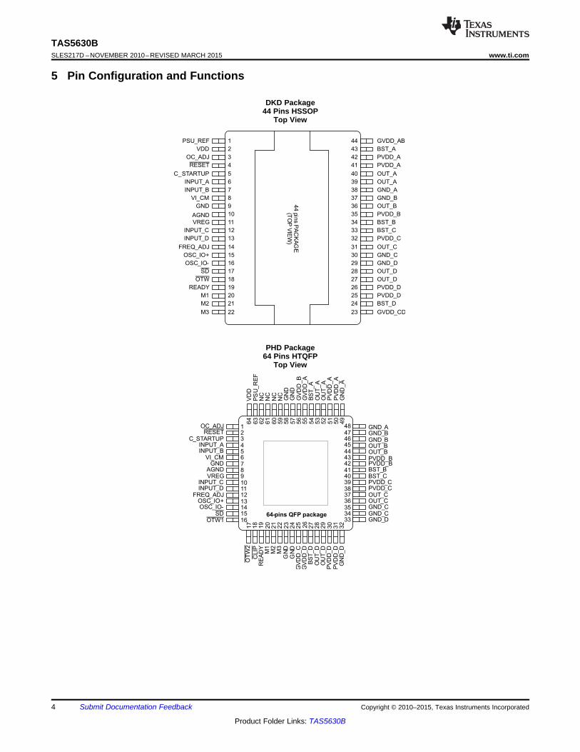
TAS5630BSLES217D –NOVEMBER 2010–REVISED MARCH 2015 www.ti.com
5 Pin Configuration and Functions
DKD Package44 Pins HSSOP
Top View
PHD Package64 Pins HTQFP
Top View
4 Submit Documentation Feedback Copyright © 2010–2015, Texas Instruments Incorporated
Product Folder Links: TAS5630B

Pin 1 Marker
White Dot
Electrical Pin 1
TAS5630Bwww.ti.com SLES217D –NOVEMBER 2010–REVISED MARCH 2015
Figure 1. Pin One Location PHD Package
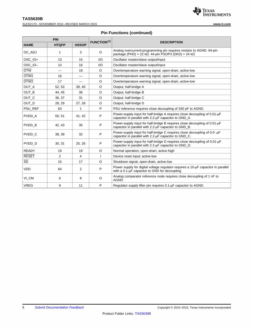
Pin FunctionsPIN
FUNCTION (1) DESCRIPTIONNAME HTQFP HSSOPAGND 8 10 P Analog groundBST_A 54 43 P HS bootstrap supply (BST), external 0.033-μF capacitor to OUT_A required.BST_B 41 34 P HS bootstrap supply (BST), external 0.033-μF capacitor to OUT_B required.BST_C 40 33 P HS bootstrap supply (BST), external 0.033-μF capacitor to OUT_C required.BST_D 27 24 P HS bootstrap supply (BST), external 0.033-μF capacitor to OUT_D required.CLIP 18 — O Clipping warning; open drain; active-lowC_STARTUP 3 5 O Start-up ramp requires a charging capacitor of 4.7 nF to AGND in BTL modeFREQ_ADJ 12 14 I PWM frame-rate-programming pin requires resistor to AGND
7, 23, 24, 57,GND 9 P Ground58GND_A 48, 49 38 P Power ground for half-bridge AGND_B 46, 47 37 P Power ground for half-bridge BGND_C 34, 35 30 P Power ground for half-bridge CGND_D 32, 33 29 P Power ground for half-bridge DGVDD_A 55 — P Gate-drive voltage supply requires 0.1-μF capacitor to GND_AGVDD_B 56 — P Gate drive voltage supply requires 0.1-μF capacitor to GND_BGVDD_C 25 — P Gate drive voltage supply requires 0.1-μF capacitor to GND_CGVDD_D 26 — P Gate drive voltage supply requires 0.1-μF capacitor to GND_DGVDD_AB — 44 P Gate drive voltage supply requires 0.22-μF capacitor to GND_A/GND_BGVDD_CD — 23 P Gate drive voltage supply requires 0.22-μF capacitor to GND_C/GND_DINPUT_A 4 6 I Input signal for half-bridge AINPUT_B 5 7 I Input signal for half-bridge BINPUT_C 10 12 I Input signal for half-bridge CINPUT_D 11 13 I Input signal for half-bridge DM1 20 20 I Mode selectionM2 21 21 I Mode selectionM3 22 22 I Mode selectionNC 59–62 – — No connect; pins may be grounded.
(1) I = Input, O = Output, P = Power
Copyright © 2010–2015, Texas Instruments Incorporated Submit Documentation Feedback 5
Product Folder Links: TAS5630B
TAS5630BSLES217D –NOVEMBER 2010–REVISED MARCH 2015 www.ti.com
Pin Functions (continued)PIN
FUNCTION (1) DESCRIPTIONNAME HTQFP HSSOP
Analog overcurrent-programming pin requires resistor to AGND. 64-pinOC_ADJ 1 3 O package (PHD) = 22 kΩ. 44-pin PSOP3 (DKD) = 24 kΩOSC_IO+ 13 15 I/O Oscillator master/slave output/inputOSC_IO– 14 16 I/O Oscillator master/slave output/inputOTW — 18 O Overtemperature warning signal, open-drain, active-lowOTW1 16 — O Overtemperature warning signal, open-drain, active-lowOTW2 17 — O Overtemperature warning signal, open-drain, active-lowOUT_A 52, 53 39, 40 O Output, half-bridge AOUT_B 44, 45 36 O Output, half-bridge BOUT_C 36, 37 31 O Output, half-bridge COUT_D 28, 29 27, 28 O Output, half-bridge DPSU_REF 63 1 P PSU reference requires close decoupling of 330 pF to AGND.
Power-supply input for half-bridge A requires close decoupling of 0.01-μFPVDD_A 50, 51 41, 42 P capacitor in parallel with 2.2-μF capacitor to GND_A.Power-supply input for half-bridge B requires close decoupling of 0.01-μFPVDD_B 42, 43 35 P capacitor in parallel with 2.2-μF capacitor to GND_B.Power-supply input for half-bridge C requires close decoupling of 0.0- μFPVDD_C 38, 39 32 P capacitor in parallel with 2.2-μF capacitor to GND_C.Power-supply input for half-bridge D requires close decoupling of 0.01-μFPVDD_D 30, 31 25, 26 P capacitor in parallel with 2.2-μF capacitor to GND_D.
READY 19 19 O Normal operation; open-drain; active-highRESET 2 4 I Device reset input; active-lowSD 15 17 O Shutdown signal, open-drain, active-low
Power supply for digital voltage regulator requires a 10-μF capacitor in parallelVDD 64 2 P with a 0.1-μF capacitor to GND for decoupling.Analog comparator reference node requires close decoupling of 1 nF toVI_CM 6 8 O AGND.
VREG 9 11 P Regulator supply filter pin requires 0.1-μF capacitor to AGND.
6 Submit Documentation Feedback Copyright © 2010–2015, Texas Instruments Incorporated
Product Folder Links: TAS5630B
TAS5630Bwww.ti.com SLES217D –NOVEMBER 2010–REVISED MARCH 2015
6 Specifications
6.1 Absolute Maximum Ratingsover operating free-air temperature range unless otherwise noted (1)
MIN MAX UNIT
VDD to AGND –0.3 13.2 V
GVDD to AGND –0.3 13.2 V
PVDD_X to GND_X (2) –0.3 69 V
OUT_X to GND_X (2) –0.3 69 V
BST_X to GND_X (2) –0.3 82.2 V
BST_X to GVDD_X (2) –0.3 69 V
VREG to AGND –0.3 4.2 V
GND_X to GND –0.3 0.3 V
GND_X to AGND –0.3 0.3 V
OC_ADJ, M1, M2, M3, OSC_IO+, OSC_IO–, FREQ_ADJ, VI_CM, C_STARTUP, PSU_REF to AGND –0.3 4.2 V
INPUT_X –0.3 7 V
RESET, SD, OTW1, OTW2, CLIP, READY to AGND –0.3 7 V
Continuous sink current (SD, OTW1, OTW2, CLIP, READY) 9 mA
Operating junction temperature, TJ 0 150 °C
Storage temperature, Tstg –40 150 °C
(1) Stresses beyond those listed under Absolute Maximum Ratings may cause permanent damage to the device. These are stress ratingsonly, and functional operation of the device at these or any other conditions beyond those indicated under Recommended OperatingConditions is not implied. Exposure to absolute-maximum-rated conditions for extended periods may affect device reliability.
(2) These voltages represents the dc voltage + peak ac waveform measured at the terminal of the device in all conditions.
6.2 ESD RatingsVALUE UNIT
Human body model (HBM), per ANSI/ESDA/JEDEC JS-001 (1) ±2000V(ESD) Electrostatic discharge VCharged-device model (CDM), per JEDEC specification JESD22- ±500
C101 (2)
(1) JEDEC document JEP155 states that 500-V HBM allows safe manufacturing with a standard ESD control process.(2) JEDEC document JEP157 states that 250-V CDM allows safe manufacturing with a standard ESD control process.
6.3 Recommended Operating Conditionsover operating free-air temperature range (unless otherwise noted)
MIN NOM MAX UNIT
PVDD_x Half-bridge supply DC supply voltage 25 50 52.5 V
GVDD_x Supply for logic regulators and gate-drive circuitry DC supply voltage 10.8 12 13.2 V
VDD Digital regulator supply voltage DC supply voltage 10.8 12 13.2 V
RL(BTL) 3.5 4Output filter according to schematics in theRL(SE) (2) Load impedance (1) 1.8 2 Ωapplication information section
RL(PBTL) (2) 2.4 3
LOUTPUT(BTL) 7 10
LOUTPUT(SE) (2) Output filter inductance (1) Minimum output inductance at IOC 7 15 μH
LOUTPUT(PBTL) (2) 7 10
Nominal 385 400 415PWM frame rate selectable for AM interferencefPWM AM1 315 333 350 kHzavoidance; 1% resistor tolerance.
AM2 260 300 335
Nominal; master mode 9.9 10 10.1
RFREQ_ADJ PWM frame-rate-programming resistor AM1; master mode 19.8 20 20.2 kΩ
AM2; master mode 29.7 30 30.3
(1) Values are for actual measured impedance over all combinations of tolerance, current and temperature and not simply the componentrating.
(2) See additional details for SE and PBTL in System Design Considerations.
Copyright © 2010–2015, Texas Instruments Incorporated Submit Documentation Feedback 7
Product Folder Links: TAS5630B

TAS5630BSLES217D –NOVEMBER 2010–REVISED MARCH 2015 www.ti.com
Recommended Operating Conditions (continued)over operating free-air temperature range (unless otherwise noted)
MIN NOM MAX UNIT
Voltage on FREQ_ADJ pin for slave modeVFREQ_ADJ Slave mode 3.3 Voperation
64-pin QFP package (PHD) 22 33Overcurrent-protection-programming resistor,cycle-by-cycle mode 44-Pin PSOP3 package (DKD) 24 33ROCP kΩOvercurrent-protection-programming resistor, PHD or DKD 47 68latching mode
TJ Junction temperature 0 125 °C
6.4 Thermal InformationTAS5630B
THERMAL METRIC (1) PHD (HTQFP) DKD (HSSOP) UNIT64 PINS 44 PINS
RθJA Junction-to-ambient thermal resistance 8.6 8.8RθJC(top) Junction-to-case (top) thermal resistance 0.3 0.4RθJB Junction-to-board thermal resistance 2.1 3.0 °C/WψJT Junction-to-top characterization parameter 0.4 0.4ψJB Junction-to-board characterization parameter 2.1 3.0
(1) For more information about traditional and new thermal metrics, see the IC Package Thermal Metrics application report (SPRA953).
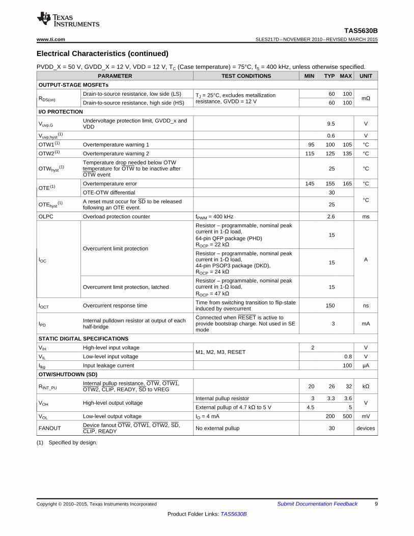
6.5 Electrical CharacteristicsPVDD_X = 50 V, GVDD_X = 12 V, VDD = 12 V, TC (Case temperature) = 75°C, fS = 400 kHz, unless otherwise specified.
PARAMETER TEST CONDITIONS MIN TYP MAX UNITINTERNAL VOLTAGE REGULATOR AND CURRENT CONSUMPTION
Voltage regulator, only used as referenceVREG VDD = 12 V 3 3.3 3.6 Vnode, VREGVI_CM Analog comparator reference node, VI_CM 1.75 2 2.15 V
Operating, 50% duty cycle 22.5IVDD VDD supply current mA
Idle, reset mode 22.550% duty cycle 12.5
IGVDD_X GVDD_x gate-supply current per half-bridge mAReset mode 1.550% duty cycle with recommended output 13.3 mAfilterIPVDD_X Half-bridge supply currentReset mode, No switching 870 μA
ANALOG INPUTSRIN Input resistance READY = HIGH 33 kΩ
Maximum input voltage with symmetricalVIN 5 VPPoutput swingIIN Maximum input current 342 μAG Voltage gain (VOUT/VIN) 23 dBOSCILLATOR
Nominal, master mode 3.85 4 4.15fOSC_IO+ AM1, master mode FPWM × 10 3.15 3.33 3.5 MHz
AM2, master mode 2.6 3 3.35VIH High level input voltage 1.86 VVIL Low level input voltage 1.45 V
8 Submit Documentation Feedback Copyright © 2010–2015, Texas Instruments Incorporated
Product Folder Links: TAS5630B
TAS5630Bwww.ti.com SLES217D –NOVEMBER 2010–REVISED MARCH 2015
Electrical Characteristics (continued)PVDD_X = 50 V, GVDD_X = 12 V, VDD = 12 V, TC (Case temperature) = 75°C, fS = 400 kHz, unless otherwise specified.
PARAMETER TEST CONDITIONS MIN TYP MAX UNITOUTPUT-STAGE MOSFETs
Drain-to-source resistance, low side (LS) 60 100TJ = 25°C, excludes metallizationRDS(on) mΩresistance, GVDD = 12 VDrain-to-source resistance, high side (HS) 60 100I/O PROTECTION
Undervoltage protection limit, GVDD_x andVuvp,G 9.5 VVDDVuvp,hyst
(1) 0.6 VOTW1 (1) Overtemperature warning 1 95 100 105 °COTW2 (1) Overtemperature warning 2 115 125 135 °C
Temperature drop needed below OTWOTWhyst
(1) temperature for OTW to be inactive after 25 °COTW eventOvertemperature error 145 155 165 °C
OTE (1)OTE-OTW differential 30
°CA reset must occur for SD to be releasedOTEhyst(1) 25following an OTE event.
OLPC Overload protection counter fPWM = 400 kHz 2.6 msResistor – programmable, nominal peakcurrent in 1-Ω load, 1564-pin QFP package (PHD)ROCP = 22 kΩ
Overcurrent limit protectionResistor – programmable, nominal peak
IOC current in 1-Ω load, A1544-pin PSOP3 package (DKD),ROCP = 24 kΩResistor – programmable, nominal peakcurrent in 1-Ω load,Overcurrent limit protection, latched 15ROCP = 47 kΩTime from switching transition to flip-stateIOCT Overcurrent response time 150 nsinduced by overcurrentConnected when RESET is active toInternal pulldown resistor at output of eachIPD provide bootstrap charge. Not used in SE 3 mAhalf-bridge mode
STATIC DIGITAL SPECIFICATIONSVIH High-level input voltage 2 V
M1, M2, M3, RESETVIL Low-level input voltage 0.8 VIlkg Input leakage current 100 μAOTW/SHUTDOWN (SD)
Internal pullup resistance, OTW, OTW1,RINT_PU 20 26 32 kΩOTW2, CLIP, READY, SD to VREGInternal pullup resistor 3 3.3 3.6
VOH High-level output voltage VExternal pullup of 4.7 kΩ to 5 V 4.5 5
VOL Low-level output voltage IO = 4 mA 200 500 mVDevice fanout OTW, OTW1, OTW2, SD,FANOUT No external pullup 30 devicesCLIP, READY
(1) Specified by design.
Copyright © 2010–2015, Texas Instruments Incorporated Submit Documentation Feedback 9
Product Folder Links: TAS5630B

TAS5630BSLES217D –NOVEMBER 2010–REVISED MARCH 2015 www.ti.com
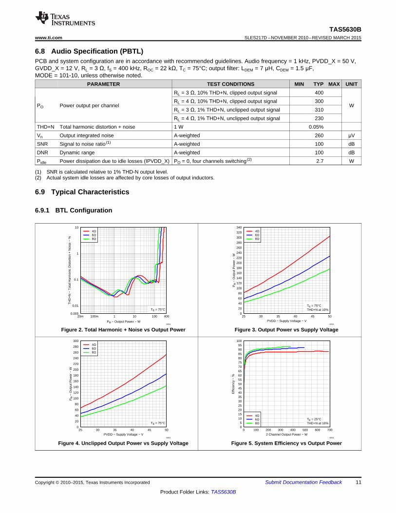
6.6 Audio Characteristics (BTL)PCB and system configuration are in accordance with recommended guidelines. Audio frequency = 1 kHz, PVDD_X = 50 V,GVDD_X = 12 V, RL = 4 Ω, fS = 400 kHz, ROC = 22 kΩ, TC = 75°C; output filter: LDEM = 7 μH, CDEM = 680 nF,MODE = 010, unless otherwise noted.
PARAMETER TEST CONDITIONS MIN TYP MAX UNITRL = 4 Ω, 10% THD+N, clipped output signal 300RL = 6 Ω, 10% THD+N, clipped output signal 210RL = 8 Ω, 10% THD+N, clipped output signal 160
PO Power output per channel WRL = 4 Ω, 1% THD+N, unclipped output signal 240RL = 6 Ω, 1% THD+N, unclipped output signal 160RL = 8 Ω, 1% THD+N, unclipped output signal 125
THD+N Total harmonic distortion + noise 1 W 0.03%A-weighted, AES17 filter, input capacitorVn Output integrated noise 270 μVgrounded
|VOS| Output offset voltage Inputs ac-coupled to AGND 20 50 mVSNR Signal-to-noise ratio (1) A-weighted, AES17 filter 100 dBDNR Dynamic range A-weighted, AES17 filter 100 dBPidle Power dissipation due to idle losses (IPVDD_X) PO = 0, four channels switching (2) 2.7 W
(1) SNR is calculated relative to 1% THD+N output level.(2) Actual system idle losses also are affected by core losses of output inductors.
6.7 Audio Specification (Single-Ended Output)PCB and system configuration are in accordance with recommended guidelines. Audio frequency = 1kHz, PVDD_X = 50 V,GVDD_X = 12 V, RL = 4 Ω, fS = 400 kHz, ROC = 22 kΩ, TC = 75°C; output filter: LDEM = 15 μH, CDEM = 470 μF,MODE = 100, unless otherwise noted.
PARAMETER TEST CONDITIONS MIN TYP MAX UNITRL = 2 Ω, 10% THD+N, clipped output signal 145RL = 3 Ω, 10% THD+N, clipped output signal 100RL = 4 Ω, 10% THD+N, clipped output signal 75
PO Power output per channel WRL = 2 Ω, 1% THD+N, unclipped output signal 110RL = 3 Ω, 1% THD+N, unclipped output signal 75RL = 4 Ω, 1% THD+N, unclipped output signal 55
THD+N Total harmonic distortion + noise 1 W 0.07%Vn Output integrated noise A-weighted, AES17 filter, input capacitor grounded 340 μVSNR Signal-to-noise ratio (1) A-weighted, AES17 filter 93 dBDNR Dynamic range A-weighted, AES17 filter 93 dB
Power dissipation due to idle lossesPidle PO = 0, four channels switching (2) 2 W(IPVDD_X)
(1) SNR is calculated relative to 1% THD+N output level.(2) Actual system idle losses are affected by core losses of output inductors.
10 Submit Documentation Feedback Copyright © 2010–2015, Texas Instruments Incorporated
Product Folder Links: TAS5630B
0
20
40
60
80
100
120
140
160
180
200
220
240
260
280
300
25 30 35 40 45 50PVDD − Supply Voltage − V
PO −
Out
put P
ower
− W
4Ω6Ω8Ω
TC = 75°C
G001
05
101520253035404550556065707580859095
100
0 100 200 300 400 500 600 7002 Channel Output Power − W
Effi
cien
cy −
%
4Ω6Ω8Ω
TC = 25°CTHD+N at 10%
G001
0.005
0.01
0.1
1
10
20m 100m 1 10 100 400
PO − Output Power − W
TH
D+
N −
Tot
al H
arm
onic
Dis
tort
ion
+ N
oise
− %
4Ω6Ω8Ω
TC = 75°C
G001
0
20
40
60
80
100
120
140
160
180
200
220
240
260
280
300
320
340
25 30 35 40 45 50PVDD − Supply Voltage − V
PO −
Out
put P
ower
− W4Ω6Ω8Ω
TC = 75°CTHD+N at 10%
G001
TAS5630Bwww.ti.com SLES217D –NOVEMBER 2010–REVISED MARCH 2015
6.8 Audio Specification (PBTL)PCB and system configuration are in accordance with recommended guidelines. Audio frequency = 1 kHz, PVDD_X = 50 V,GVDD_X = 12 V, RL = 3 Ω, fS = 400 kHz, ROC = 22 kΩ, TC = 75°C; output filter: LDEM = 7 μH, CDEM = 1.5 μF,MODE = 101-10, unless otherwise noted.
PARAMETER TEST CONDITIONS MIN TYP MAX UNITRL = 3 Ω, 10% THD+N, clipped output signal 400RL = 4 Ω, 10% THD+N, clipped output signal 300
PO Power output per channel WRL = 3 Ω, 1% THD+N, unclipped output signal 310RL = 4 Ω, 1% THD+N, unclipped output signal 230
THD+N Total harmonic distortion + noise 1 W 0.05%Vn Output integrated noise A-weighted 260 μVSNR Signal to noise ratio (1) A-weighted 100 dBDNR Dynamic range A-weighted 100 dBPidle Power dissipation due to idle losses (IPVDD_X) PO = 0, four channels switching (2) 2.7 W
(1) SNR is calculated relative to 1% THD-N output level.(2) Actual system idle losses are affected by core losses of output inductors.
6.9 Typical Characteristics
6.9.1 BTL Configuration
Figure 2. Total Harmonic + Noise vs Output Power Figure 3. Output Power vs Supply Voltage
Figure 4. Unclipped Output Power vs Supply Voltage Figure 5. System Efficiency vs Output Power
Copyright © 2010–2015, Texas Instruments Incorporated Submit Documentation Feedback 11
Product Folder Links: TAS5630B

0.005
0.01
0.1
1
10
20m 100m 1 10 100 200
PO − Output Power − W
TH
D+
N −
Tot
al H
arm
onic
Dis
tort
ion
+ N
oise
− %
2Ω3Ω4Ω
TC = 75°C
G001
0
10
20
30
40
50
60
70
80
90
100
110
120
130
140
150
160
170
25 30 35 40 45 50PVDD − Supply Voltage − V
PO −
Out
put P
ower
− W
2Ω3Ω4Ω
TC = 75°CTHD+N at 10%
G001
−160
−150
−140
−130
−120
−110
−100
−90
−80
−70
−60
−50
−40
−30
−20
−10
0
0 2k 4k 6k 8k 10k 12k 14k 16k 18k 20k 22kf − Frequency − Hz
Noi
se A
mpl
itude
− d
B
4ΩTC = 75°CVREF = 35.36 VSample Rate = 48kHzFFT Size = 16384
G001
05
101520253035404550556065707580859095
100
0 100 200 300 400 500 600 7002 Channel Output Power − W
Pow
er L
oss
− W
4Ω6Ω8Ω
TC = 25°CTHD+N at 10%
G001
0
20
40
60
80
100
120
140
160
180
200
220
240
260
280
300
320
340
−10 0 10 20 30 40 50 60 70 80 90 100 110
TC − Case Temperature − °C
PO −
Out
put P
ower
− W
4Ω6Ω8Ω THD+N at 10%
G001
TAS5630BSLES217D –NOVEMBER 2010–REVISED MARCH 2015 www.ti.com
BTL Configuration (continued)
Figure 6. System Power Loss vs Output Power Figure 7. Output Power vs Case Temperature
Figure 8. Noise Amplitude vs Frequency
6.9.2 SE Configuration1 Channel Driven
Figure 9. Total Harmonic Distortion + Noise vs Output Figure 10. Output Power vs Supply VoltagePower
12 Submit Documentation Feedback Copyright © 2010–2015, Texas Instruments Incorporated
Product Folder Links: TAS5630B

0
50
100
150
200
250
300
350
400
450
500
−10 0 10 20 30 40 50 60 70 80 90 100 110
TC − Case Temperature − °C
PO −
Out
put P
ower
− W
3Ω4Ω6Ω8Ω THD+N at 10%
G001
0.005
0.01
0.1
1
10
20m 100m 1 10 100 700
PO − Output Power − W
TH
D+
N −
Tot
al H
arm
onic
Dis
tort
ion
+ N
oise
− %
3Ω4Ω6Ω8Ω
TC = 75°C
G001
0
50
100
150
200
250
300
350
400
450
500
25 30 35 40 45 50PVDD − Supply Voltage − V
PO −
Out
put P
ower
− W
3Ω4Ω6Ω8Ω
TC = 75°CTHD+N at 10%
G001
0
10
20
30
40
50
60
70
80
90
100
110
120
130
140
150
160
170
180
−10 0 10 20 30 40 50 60 70 80 90 100 110
TC − Case Temperature − °C
PO −
Out
put P
ower
− W
2Ω3Ω4Ω THD+N at 10%
G001
TAS5630Bwww.ti.com SLES217D –NOVEMBER 2010–REVISED MARCH 2015
SE Configuration (continued)
Figure 11. Output Power vs Case Temperature
6.9.3 PBTL Configuration
Figure 12. Total Harmonic Distortion + Noise vs Output Figure 13. Output Power vs Supply VoltagePower
Figure 14. Output Power vs Case Temperature
Copyright © 2010–2015, Texas Instruments Incorporated Submit Documentation Feedback 13
Product Folder Links: TAS5630B

M1
M2
/RESET
/SD
/OTW2
AGND
OC_ADJ
VREG
VDD
GVDD_A
M3
GND
INPUT_D
OUT_A
GND_A
PVDD_A
BST_A
GVDD_A
PWM
ACTIVITY
DETECTOR
GVDD_C
GVDD_B
INPUT_C
OUT_B
GND_B
PVDD_B
BST_B
GVDD_B GVDD_D
GVDD_C
OUT_C
GND_C
PVDD_C
BST_C
GVDD_D
OUT_D
GND_D
PVDD_D
BST_D
INPUT_B
INPUT_A
PVDD_XOUT_XGND_X
TIMING
CONTROLCONTROL GATE-DRIVE
TIMING
CONTROLCONTROL GATE-DRIVE
TIMINGCONTROL
CONTROL GATE-DRIVE
TIMING
CONTROLCONTROL GATE-DRIVE
PWMRECEIVER
PWM
RECEIVER
PWM
RECEIVER
PWM
RECEIVER
+
-
AN
AL
OG
CO
MP
AR
ATO
RM
UX
+
-
+
-
+
-
PR
OT
EC
TIO
N&
I/O
LO
GIC
VI_CM
STARTUP
CONTROL
POWER-UP
RESET
TEMPSENSE
OVER-LOAD
PROTECTION
PPSC
CB3C
UVP
CURRENT
SENSE
VREG
C_STARTUP
ANALOG
LOOP FILTER
ANALOG
LOOP FILTER
ANALOG
LOOP FILTER
ANALOG
LOOP FILTER
OSCILLATOR
FREQ_ADJ
OSC_SYNC_IO-
AN
AL
OG
INP
UT
MU
X
PSU_FFPSU_REF
4
4
4
PVDD_X4
GND
OSC_SYNC_IO+
/OTW1
READY
/CLIP
TAS5630BSLES217D –NOVEMBER 2010–REVISED MARCH 2015 www.ti.com
7 Detailed Description
7.1 OverviewTAS5630B is an analog input, audio PWM (class-D) amplifier. The output of the TAS5630B can be configured forsingle-ended, bridge-tied load (BTL) or parallel BTL (PBTL) output. It requires two rails for power supply, PVDDand 12 V (GVDD and VDD). The following functional block diagram shows interconnections of internal supplies,control logic, gate drives and power amplifiers. Detailed schematic can be viewed in TAS5630B EVM User'sGuide (SLAU287).
7.2 Functional Block Diagram
14 Submit Documentation Feedback Copyright © 2010–2015, Texas Instruments Incorporated
Product Folder Links: TAS5630B

TAS5630Bwww.ti.com SLES217D –NOVEMBER 2010–REVISED MARCH 2015
7.3 Feature Description
7.3.1 Power SuppliesTo facilitate system design, the TAS5630B needs only a 12-V supply in addition to the (typical) 50-V power-stagesupply. An internal voltage regulator provides suitable voltage levels for the digital and low-voltage analogcircuitry. Additionally, all circuitry requiring a floating voltage supply, for example, the high-side gate drive, isaccommodated by built-in bootstrap circuitry requiring only an external capacitor for each half-bridge.
To provide outstanding electrical and acoustical characteristics, the PWM signal path, including gate drive andoutput stage, is designed as identical, independent half-bridges. For this reason, each half-bridge has separategate drive supply pins (GVDD_X), bootstrap pins (BST_X), and power-stage supply pins (PVDD_X).Furthermore, an additional pin (VDD) is provided as supply for all common circuits. Although supplied from thesame 12-V source, it is highly recommended to separate GVDD_A, GVDD_B, GVDD_C, GVDD_D, and VDD onthe printed-circuit board (PCB) by RC filters (see Typical Application for details). These RC filters provide therecommended high-frequency isolation. Special attention should be paid to placing all decoupling capacitors asclose to their associated pins as possible. In general, inductance between the power supply pins and decouplingcapacitors must be avoided. (See SLAU287 for additional information.)
For a properly functioning bootstrap circuit, a small ceramic capacitor must be connected from each bootstrap pin(BST_X) to the power-stage output pin (OUT_X). When the power-stage output is low, the bootstrap capacitor ischarged through an internal diode connected between the gate-drive power-supply pin (GVDD_X) and thebootstrap pin. When the power-stage output is high, the bootstrap capacitor potential is shifted above the outputpotential and thus provides a suitable voltage supply for the high-side gate driver. In an application with PWMswitching frequencies in the range from 300 kHz to 400 kHz, it is recommended to use 33-nF ceramic capacitors,size 0603 or 0805, for the bootstrap supply. These 33-nF capacitors ensure sufficient energy storage, evenduring minimal PWM duty cycles, to keep the high-side power stage FET (LDMOS) fully turned on during theremaining part of the PWM cycle.
Special attention should be paid to the power-stage power supply; this includes component selection, PCBplacement, and routing. As indicated, each half-bridge has independent power-stage supply pins (PVDD_X). Foroptimal electrical performance, EMI compliance, and system reliability, it is important that each PVDD_X pin isdecoupled with a 2.2-μF ceramic capacitor placed as close as possible to each supply pin. It is recommended tofollow the PCB layout of the TAS5630B reference design. For additional information on recommended powersupply and required components, see Typical Application.
The 12-V supply should be from a low-noise, low-output-impedance voltage regulator. Likewise, the 50-V power-stage supply is assumed to have low output impedance and low noise. The power-supply sequence is not criticalas facilitated by the internal power-on-reset circuit. Moreover, the TAS5630B is fully protected against erroneouspower-stage turnon due to parasitic gate charging. Thus, voltage-supply ramp rates (dV/dt) are non-critical withinthe specified range (see Recommended Operating Conditions).
7.3.2 System Power-Up and Power-Down Sequence
7.3.2.1 Powering UpThe TAS5630B does not require a power-up sequence. The outputs of the H-bridges remain in a high-impedance state until the gate-drive supply voltage (GVDD_X) and VDD voltage are above the undervoltageprotection (UVP) voltage threshold (see Electrical Characteristics). Although not specifically required, it isrecommended to hold RESET in a low state while powering up the device. This allows an internal circuit tocharge the external bootstrap capacitors by enabling a weak pulldown of the half-bridge output.
7.3.2.2 Powering DownThe TAS5630B does not require a power-down sequence. The device remains fully operational as long as thegate-drive supply (GVDD_X) voltage and VDD voltage are above the undervoltage protection (UVP) voltagethreshold (see Electrical Characteristics). Although not specifically required, it is a good practice to hold RESETlow during power down, thus preventing audible artifacts including pops or clicks.
7.3.3 Error ReportingThe SD, OTW, OTW1, and OTW2 pins are active-low, open-drain outputs. Their function is for protection-modesignaling to a PWM controller or other system-control device.
Copyright © 2010–2015, Texas Instruments Incorporated Submit Documentation Feedback 15
Product Folder Links: TAS5630B

TAS5630BSLES217D –NOVEMBER 2010–REVISED MARCH 2015 www.ti.com
Feature Description (continued)Any fault resulting in device shutdown is signaled by the SD pin going low. Likewise, OTW and OTW2 go lowwhen the device junction temperature exceeds 125°C and OTW1 goes low when the junction temperatureexceeds 100°C (see Table 1).
Table 1. Error ReportingOTW2,SD OTW1 DESCRIPTIONOTW
0 0 0 Overtemperature (OTE) or overload (OLP) or undervoltage (UVP)Overload (OLP) or undervoltage (UVP). Junction temperature higher than 100°C (overtemperature0 0 1 warning)
0 1 1 Overload (OLP) or undervoltage (UVP)1 0 0 Junction temperature higher than 125°C (overtemperature warning)1 0 1 Junction temperature higher than 100°C (overtemperature warning)1 1 1 Junction temperature lower than 100°C and no OLP or UVP faults (normal operation)
Note that asserting either RESET low forces the SD signal high, independent of faults being present. TIrecommends monitoring the OTW signal using the system microcontroller and responding to an overtemperaturewarning signal by, for example, turning down the volume to prevent further heating of the device resulting indevice shutdown (OTE).
To reduce external component count, an internal pullup resistor to 3.3 V is provided on both SD and OTWoutputs. Level compliance for 5-V logic can be obtained by adding external pullup resistors to 5 V (see ElectricalCharacteristics for further specifications).
7.3.4 Device Protection SystemThe TAS5630B contains advanced protection circuitry carefully designed to facilitate system integration and easeof use, as well as to safeguard the device from permanent failure due to a wide range of fault conditions such asshort circuits, overload, overtemperature, and undervoltage. The TAS5630B responds to a fault by immediatelysetting the power stage in a high-impedance (Hi-Z) state and asserting the SD pin low. In situations other thanoverload and overtemperature error (OTE), the device automatically recovers when the fault condition has beenremoved, that is, the supply voltage has increased.
The device functions on errors, as shown in the following table.
Table 2. Device Protection SystemBTL Mode PBTL Mode SE Mode
Local error in Turns Off or in Local error in Turns Off or in Local error in Turns Off or inA A A
A + B A + BB B B
A + B + C + DC C C
C + D C + DD D D
Bootstrap UVP does not shut down according to the table; it shuts down the respective half-bridge.
16 Submit Documentation Feedback Copyright © 2010–2015, Texas Instruments Incorporated
Product Folder Links: TAS5630B

TAS5630Bwww.ti.com SLES217D –NOVEMBER 2010–REVISED MARCH 2015
7.3.5 Pin-to-Pin Short-Circuit Protection (PPSC)The PPSC detection system protects the device from permanent damage if a power output pin (OUT_X) isshorted to GND_X or PVDD_X. For comparison, the OC protection system detects an overcurrent after thedemodulation filter, whereas PPSC detects shorts directly at the pin before the filter. PPSC detection isperformed at startup, that is, when VDD is supplied; consequently, a short to either GND_X or PVDD_X aftersystem startup does not activate the PPSC detection system. When PPSC detection is activated by a short onthe output, all half-bridges are kept in a Hi-Z state until the short is removed; the device then continues thestartup sequence and starts switching. The detection is controlled globally by a two-step sequence. The first stepensures that there are no shorts from OUT_X to GND_X; the second step tests that there are no shorts fromOUT_X to PVDD_X. The total duration of this process is roughly proportional to the capacitance of the output LCfilter. The typical duration is <15 ms/μF. While the PPSC detection is in progress, SD is kept low, and the devicedoes not react to changes applied to the RESET pins. If no shorts are present the PPSC detection passes, andSD is released, a device reset does not start a new PPSC detection. PPSC detection is enabled in BTL andPBTL output configurations; the detection is not performed in SE mode. To make sure the PPSC detectionsystem is not tripped, it is recommended not to insert resistive load between OUT_X and GND_X or PVDD_X.
7.3.6 Overtemperature ProtectionThe two different package options have individual overtemperature protection schemes.
PHD Package:The TAS5630B PHD package option has a three-level temperature-protection system that asserts an active-lowwarning signal (OTW1) when the device junction temperature exceeds 100°C (typical), (OTW2) when the devicejunction temperature exceeds 125°C (typical) and, if the device junction temperature exceeds 155°C (typical), thedevice is put into thermal shutdown, resulting in all half-bridge outputs being set in the high-impedance (Hi-Z)state and SD being asserted low. OTE is latched in this case. To clear the OTE latch, RESET must be asserted.Thereafter, the device resumes normal operation. For highest reliability, the RESET should not be asserted untilOTW1 has cleared.
DKD Package:The TAS5630B DKD package option has a two-level temperature-protection system that asserts an active-lowwarning signal (OTW) when the device junction temperature exceeds 125°C (typical) and, if the device junctiontemperature exceeds 155°C (typical), the device is put into thermal shutdown, resulting in all half-bridge outputsbeing set in the high-impedance (Hi-Z) state and SD being asserted low. OTE is latched in this case. To clear theOTE latch, RESET must be asserted. It is recommended to wait until OTW has cleared before asserting RESET.Thereafter, the device resumes normal operation.
7.3.7 Undervoltage Protection (UVP) and Power-On Reset (POR)The UVP and POR circuits of the TAS5630B fully protect the device in any power-up/down and brownoutsituation. While powering up, the POR circuit resets the overload circuit (OLP) and ensures that all circuits arefully operational when the GVDD_X and VDD supply voltages reach the levels stated in ElectricalCharacteristics. Although GVDD_X and VDD are independently monitored, a supply voltage drop below the UVPthreshold on any VDD or GVDD_X pin results in all half-bridge outputs immediately being set in the high-impedance (Hi-Z) state and SD being asserted low. The device automatically resumes operation when all supplyvoltages have increased above the UVP threshold.
7.3.8 Device ResetWhen RESET is asserted low, all power-stage FETs in the four half-bridges are forced into a high-impedance(Hi-Z) state.
In BTL modes, to accommodate bootstrap charging prior to switching start, asserting the reset input low enablesweak pulldown of the half-bridge outputs. In the SE mode, the output is forced into a high-impedance state whenasserting the reset input low. Asserting reset input low removes any fault information to be signaled on the SDoutput; that is, SD is forced high. A rising-edge transition on reset input allows the device to resume operationafter an overload fault. To ensure thermal reliability, the rising edge of reset must occur no sooner than 4 msafter the falling edge of SD.
Copyright © 2010–2015, Texas Instruments Incorporated Submit Documentation Feedback 17
Product Folder Links: TAS5630B
TAS5630BSLES217D –NOVEMBER 2010–REVISED MARCH 2015 www.ti.com
7.3.9 Click and Pop in SE-ModeThe BTL startup has low click and pop due to the trimmed output dc offset, see Audio Characteristics (BTL).
The startup of the BTL+2 x SE system (Figure 21) or 4xSE (Figure 20) is more difficult to get click and pop free,than the pure BTL solution; therefore, evaluating the resulting click and pop before designing in the device isrecommended.
7.3.10 PBTL Overload and Short CircuitThe TAS5630B has extensive overload and short circuit protection. In BTL and SE mode, it is fully protectedagainst speaker terminal overloads, terminal-to-terminal short circuit, and short circuit to GND or PVDD. Theprotection works by limiting the current, by flipping the state of the output MOSFETs; thereby, ramping currentsdown in the inductor. This only works when the inductor is NOT saturated, the recommended minimum inductorvalues are listed in Recommended Operating Conditions. In BTL mode, the short circuit currents can reach morethan 15 A, so when connecting the device in PBTL mode (Mono), the currents double – that is more than 30 A,and with these high currents, the protection system will limit PBTL speaker overloads, terminal-to-terminal shorts,and terminal-to-GND shorts. PBTL mode short circuit to PVDD is not recommended.
7.3.11 OscillatorThe oscillator frequency can be trimmed by external control of the FREQ_ADJ pin.
To reduce interference problems while using a radio receiver tuned within the AM band, the switching frequencycan be changed from nominal to lower values. These values should be chosen such that the nominal and thelower-value switching frequencies together result in the fewest cases of interference throughout the AM band,and can be selected by the value of the FREQ_ADJ resistor connected to AGND in master mode.
For slave-mode operation, turn off the oscillator by pulling the FREQ_ADJ pin to VREG. This configures theOSC_I/O pins as inputs, which must be slaved from an external clock.
7.4 Device Functional Modes
Table 3. Mode Selection PinsMODE PINS OUTPUTANALOG INPUT DESCRIPTIONCONFIGURATIONM3 M2 M1
0 0 0 Differential 2 × BTL AD mode0 0 1 — — Reserved0 1 0 Differential 2 × BTL BD mode
Differential single-0 1 1 1 × BTL +2 ×SE BD mode, BTL differentialended1 0 0 Single-ended 4 × SE AD mode
INPUT_C (1) INPUT_D (1)
1 0 1 Differential 1 × PBTL 0 0 AD mode1 0 BD mode
1 1 0Reserved
1 1 1
(1) INPUT_C and D are used to select between a subset of AD and BD mode operations in PBTL mode (1=VREG and 0=AGND).
18 Submit Documentation Feedback Copyright © 2010–2015, Texas Instruments Incorporated
Product Folder Links: TAS5630B

TAS5630Bwww.ti.com SLES217D –NOVEMBER 2010–REVISED MARCH 2015
8 Application and Implementation
NOTEInformation in the following applications sections is not part of the TI componentspecification, and TI does not warrant its accuracy or completeness. TI’s customers areresponsible for determining suitability of components for their purposes. Customers shouldvalidate and test their design implementation to confirm system functionality.
8.1 Application Information
8.1.1 PCB Material RecommendationTI recommends FR-4 2-oz. (70-μm) glass epoxy material for use with the TAS5630B. The use of this materialcan provide for higher power output, improved thermal performance, and better EMI margin (due to lower PCBtrace resistance).
8.1.2 PVDD Capacitor RecommendationThe large capacitors used in conjunction with each full bridge are referred to as the PVDD capacitors. Thesecapacitors should be selected for proper voltage margin and adequate capacitance to support the powerrequirements. In practice, with a well-designed system power supply, 1000 μF, 63-V supports more applications.The PVDD capacitors should be the low-ESR type, because they are used in a circuit associated with high-speedswitching.
8.1.3 Decoupling Capacitor RecommendationsTo design an amplifier that has robust performance, passes regulatory requirements, and exhibits good audioperformance, quality decoupling capacitors should be used. In practice, X7R should be used in this application.
The voltage of the decoupling capacitors should be selected in accordance with good design practices.Temperature, ripple current, and voltage overshoot must be considered. This fact is particularly true in theselection of the 2.2-μF capacitor that is placed on the power supply to each half-bridge. The decoupling capacitormust withstand the voltage overshoot of the PWM switching, the heat generated by the amplifier during highpower output, and the ripple current created by high power output. A minimum voltage rating of 63 V is requiredfor use with a 50-V power supply.
8.1.4 System Design ConsiderationsA rising-edge transition on the reset input allows the device to execute the startup sequence and starts switching.
Apply audio only when the state of READY is high; that starts and stops the amplifier without having audibleartifacts that are heard in the output transducers. If an overcurrent protection event is introduced, the READYsignal goes low; hence, filtering is needed if the signal is intended for audio muting in non-microcontrollersystems.
The CLIP signal indicates that the output is approaching clipping. The signal can be used either to activate avolume decrease or to signal an intelligent power supply to increase the rail voltage from low to high for optimumefficiency.
The device inverts the audio signal from input to output.
The VREG pin is not recommended to be used as a voltage source for external circuitry.
Copyright © 2010–2015, Texas Instruments Incorporated Submit Documentation Feedback 19
Product Folder Links: TAS5630B

2-CHANNELH-BRIDGEBTL MODE
Output
H-Bridge 2
PV
DD
_A
,B
,C
,D
GN
D_
A,
B,C
,D
Hardwire
Over-
Current
Limit
8
GN
D
VD
D
VR
EG
AG
ND
OC
_A
DJ
PVDDPower Supply
Decoupling
GVDD, VDD,
& VREGPower Supply
Decoupling
SYSTEM
Power
Supplies
PVDD
GVDD (12V)/VDD (12V)
GND
50V
12V
GND
VAC
Bootstrap
Caps
BST_C
BST_D
2nd
Order
L-C Output
Filter for
each
H-Bridge
OUT_C
OUT_D
GV
DD
_A
,B
,C
,D
Bootstrap
Caps
BST_A
BST_B
INPUT_A 2nd
Order
L-C Output
Filter for
each
H-Bridge
OUT_A
OUT_B
8 4
Output
H-Bridge 1
Input
H-Bridge 1INPUT_B
M2
M1
M3
Hardwire
Mode
Control
Input
H-Bridge 2
INPUT_C
INPUT_D
VI_
CM
C_S
TA
RT
UP
PS
U_R
EF
Caps for
External
Filtering
&
Startup/Stop
Input DC
Blocking
Caps
Input DC
Blocking
Caps
/RE
SE
T
/OT
W1
,/O
TW
2,/O
TW
/CLIP
System
microcontroller
or
Analog circuitry
RE
AD
Y
/SD
ANALOG_IN_A
ANALOG_IN_B
ANALOG_IN_C
ANALOG_IN_D
FREQ_ADJ
Hardwire
PWM Frame
Rate Adjust
&
Master/Slave
Mode
OSC_IO+
OSC_IO-
Oscillator
Synchronization
2
2
2
2
(2)
TAS5630BSLES217D –NOVEMBER 2010–REVISED MARCH 2015 www.ti.com
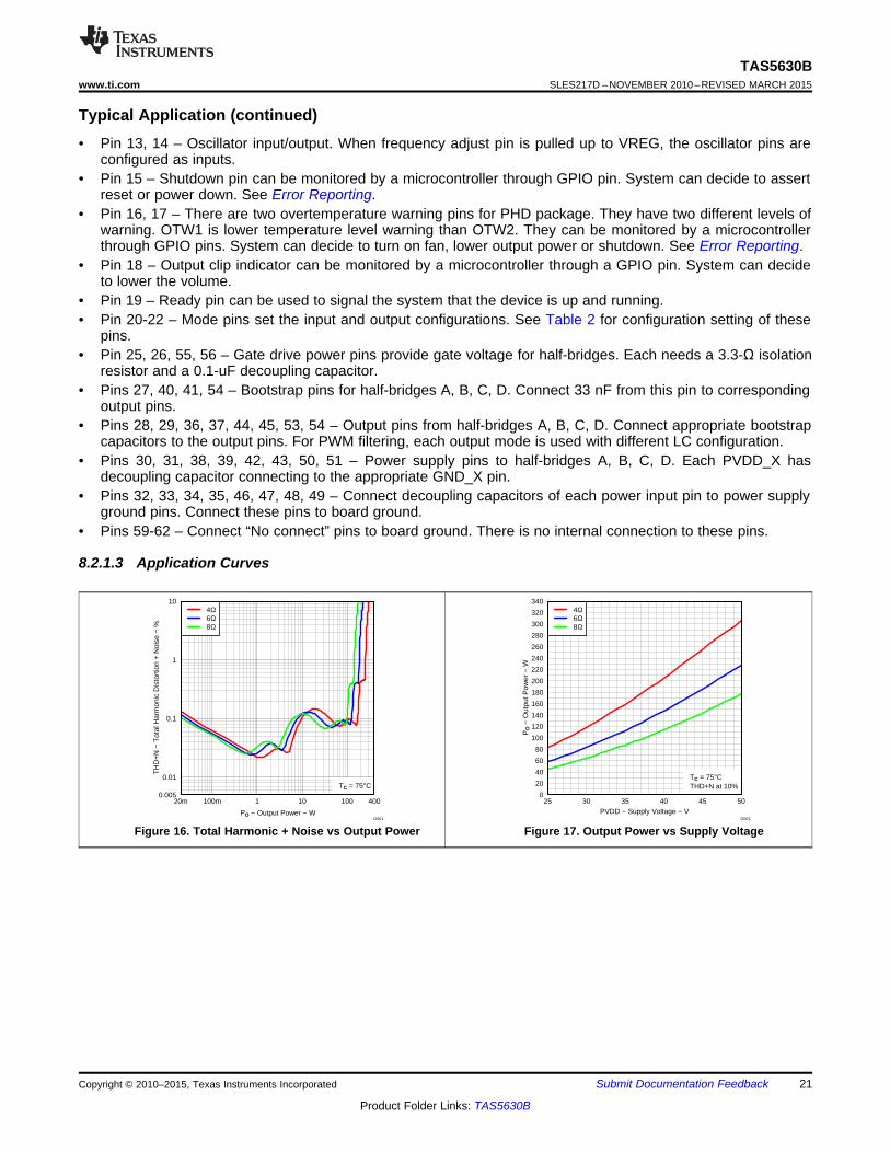
8.2 Typical ApplicationThe following schematics and PCB layouts illustrate best practices used for the TAS5630B.
8.2.1 Typical Application Schematic
Figure 15. Typical Application Schematic
8.2.1.1 Design RequirementsThis device can be configured for BTL, PBTL, or SE mode. Each mode will require a different outputconfiguration.
8.2.1.2 Detailed Design Procedure• Pin 1 – Overcurrent adjust resistor can be between 24 kΩ to 68 kΩ depending on the application. The lower
resistance corresponds to the higher over-current protection level.• Pin 2 – RESET pin when asserted, it keeps outputs Hi-Z and no PWM switching. This pin can be controlled
by a microprocessor.• Pin 3 – Start-up ramp capacitor should be 4.7 nF for BTL and PBTL configurations, and 10 nF for SE
configuration.• Pins 4, 5, 10, 11 – Differential pair inputs AB and CD. A DC blocking capacitor of 10 µF and an RC of 100 Ω
and 100 pF should be placed on each analog input.• Pin 6 – Analog comparator reference node requires close decoupling capacitor of 1 nF to ground.• Pin 7, 8, 23, 24, 57, 58 – Ground pins are connected to board ground.• Pin 9 – Regulator supply filter pin requires 0.1 uF to AGND.• Pin 12 – Frequency adjust resistor is discussed in Oscillator.
20 Submit Documentation Feedback Copyright © 2010–2015, Texas Instruments Incorporated
Product Folder Links: TAS5630B
0.005
0.01
0.1
1
10
20m 100m 1 10 100 400
PO − Output Power − W
TH
D+
N −
Tot
al H
arm
onic
Dis
tort
ion
+ N
oise
− %
4Ω6Ω8Ω
TC = 75°C
G001
0
20
40
60
80
100
120
140
160
180
200
220
240
260
280
300
320
340
25 30 35 40 45 50PVDD − Supply Voltage − V
PO −
Out
put P
ower
− W
4Ω6Ω8Ω
TC = 75°CTHD+N at 10%
G001
TAS5630Bwww.ti.com SLES217D –NOVEMBER 2010–REVISED MARCH 2015
Typical Application (continued)• Pin 13, 14 – Oscillator input/output. When frequency adjust pin is pulled up to VREG, the oscillator pins are
configured as inputs.• Pin 15 – Shutdown pin can be monitored by a microcontroller through GPIO pin. System can decide to assert
reset or power down. See Error Reporting.• Pin 16, 17 – There are two overtemperature warning pins for PHD package. They have two different levels of
warning. OTW1 is lower temperature level warning than OTW2. They can be monitored by a microcontrollerthrough GPIO pins. System can decide to turn on fan, lower output power or shutdown. See Error Reporting.
• Pin 18 – Output clip indicator can be monitored by a microcontroller through a GPIO pin. System can decideto lower the volume.
• Pin 19 – Ready pin can be used to signal the system that the device is up and running.• Pin 20-22 – Mode pins set the input and output configurations. See Table 2 for configuration setting of these
pins.• Pin 25, 26, 55, 56 – Gate drive power pins provide gate voltage for half-bridges. Each needs a 3.3-Ω isolation
resistor and a 0.1-uF decoupling capacitor.• Pins 27, 40, 41, 54 – Bootstrap pins for half-bridges A, B, C, D. Connect 33 nF from this pin to corresponding
output pins.• Pins 28, 29, 36, 37, 44, 45, 53, 54 – Output pins from half-bridges A, B, C, D. Connect appropriate bootstrap
capacitors to the output pins. For PWM filtering, each output mode is used with different LC configuration.• Pins 30, 31, 38, 39, 42, 43, 50, 51 – Power supply pins to half-bridges A, B, C, D. Each PVDD_X has
decoupling capacitor connecting to the appropriate GND_X pin.• Pins 32, 33, 34, 35, 46, 47, 48, 49 – Connect decoupling capacitors of each power input pin to power supply
ground pins. Connect these pins to board ground.• Pins 59-62 – Connect “No connect” pins to board ground. There is no internal connection to these pins.
8.2.1.3 Application Curves
Figure 16. Total Harmonic + Noise vs Output Power Figure 17. Output Power vs Supply Voltage
Copyright © 2010–2015, Texas Instruments Incorporated Submit Documentation Feedback 21
Product Folder Links: TAS5630B
IN_LEFT_N
IN_LEFT_P
R_RIGHT_N
IN_RIGHT_P
/RESET
/SD
/OTW1
/OTW2
/CLIP
READY
OSC_IO+
OSC_IO-
GVDD/VDD (+12V)
PVDD
GVDD/VDD (+12V)
PVDD
PVDD
GND
GND
GND
GND
GND
GND
GND
GND
GND
GND
GND
GND
GND
GND
GND
GND
GND
VREG
GND
GND
GND
GND
GND
GND
GND
VREG
VREG
GND
GND
GND
GND
GND
GND
GND
OUT_LEFT_P
OUT_LEFT_M
+
-
OUT_RIGHT_P
OUT_RIGHT_M
+
-
17
62
63
18
19
64
20
21
24
23
22
25
2726
29
28
30
31
32
1
33
34
35
37
2
3
36
4
38
39
5
6
7
40
418
9
42
10
43
11
44
45
12
46
47
13
48
14
15
49
16
50
51
52
54
53
56
55
57
58
59
60
61
C23
330pF
C23
330pF
R71
3.3R
R71
3.3R
C15
100pF
C15
100pF
R723.3RR723.3R
C30
100nFC30
100nF
C33
100nF
C33
100nF
C20
4.7nF
C20
4.7nF
C61
2.2uF
C61
2.2uF
R733.3RR733.3R
R32
3.3R
R32
3.3R
C721nFC721nF
R21
10k
R21
10k
C602.2uFC602.2uF
L11
7uH
L11
7uH
C53680nFC53680nF
C22
100nF
C22
100nF
R30
3.3R
R30
3.3R
C18
100pF
C18
100pF
C50680nFC50680nF
R31
3.3R
R31
3.3R
C52680nFC52680nF
C64
1000uF
C64
1000uF
L107uHL107uH
C32
100nF
C32
100nF
C7710nFC7710nF
C17
100pF
C17
100pF
C41
33nF
C41
33nF
R703.3RR703.3R
C11
100pF
C11
100pF
C4033nFC4033nF
R11
100R
R11
100R
L127uHL127uH
R33
3.3R
R33
3.3R
C66
1000uF
C66
1000uF
C42
33nF
C42
33nF
C16
10uF
C16
10uF
C692.2uFC692.2uF
C14
10uF
C14
10uF
C78
10nF
C78
10nF
R19
47k
R19
47k
C12
10uF
C12
10uF
R13
100R
R13
100R
L13
7uH
L13
7uH
C7410nFC7410nF
C26100nFC26100nF
C21
1nF
C21
1nF
C2510uFC2510uF
C10
10uF
C10
10uF
C67
1000uF
C67
1000uF
R10
100R
R10
100R
C51680nFC51680nF
C701nFC701nF
R18
100R
R18
100R
C4333nFC4333nF
C75
10nF
C75
10nF
C622.2uFC622.2uF
R20
22.0k
R20
22.0k
C65
1000uF
C65
1000uF
C13100pF
C13100pF
C711nFC711nF
C31
100nFC31
100nF
C632.2uFC632.2uF
C731nFC731nF
R74
3.3R
R74
3.3R
R12
100R
R12
100R
C7610nFC7610nF
C6847uF
63V
C6847uF
63V
U10
TAS5630BPHD
OC_ADJ
/RESET
C_STARTUP
INPUT_A
INPUT_B
VI_CM
GND
AGND
VREG
INPUT_C
INPUT_D
FREQ_ADJ
OSC_IO+
OSC_IO-
/SD
/OTW1
/OT
W2
/CL
IP
RE
AD
Y
M1
M2
M3
GN
D
GN
D
GV
DD
_C
GV
DD
_D
BS
T_
D
OU
T_
D
OU
T_
D
PV
DD
_D
PV
DD
_D
GN
D_
D
GND_A
GND_B
GND_B
OUT_B
OUT_B
PVDD_B
PVDD_B
BST_B
BST_C
PVDD_C
PVDD_C
OUT_C
OUT_C
GND_C
GND_C
GND_D
VD
D
PS
U_
RE
F
NC
NC
NC
NC
GN
D
GN
D
GV
DD
_B
GV
DD
_A
BS
T_
A
OU
T_
A
OU
T_
A
PV
DD
_A
PV
DD
_A
GN
D_
A
TAS5630BSLES217D –NOVEMBER 2010–REVISED MARCH 2015 www.ti.com
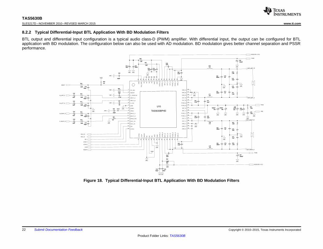
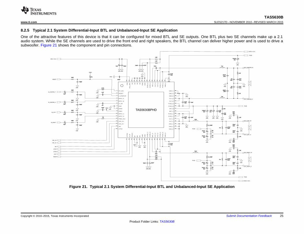
8.2.2 Typical Differential-Input BTL Application With BD Modulation FiltersBTL output and differential input configuration is a typical audio class-D (PWM) amplifier. With differential input, the output can be configured for BTLapplication with BD modulation. The configuration below can also be used with AD modulation. BD modulation gives better channel separation and PSSRperformance.
Figure 18. Typical Differential-Input BTL Application With BD Modulation Filters
22 Submit Documentation Feedback Copyright © 2010–2015, Texas Instruments Incorporated
Product Folder Links: TAS5630B

IN_N
IN_P
/RESET
/SD
/OTW1
/OTW2
/CLIP
READY
GVDD (+12V)
PVDD
OSC_IO+
OSC_IO-
GVDD (+12V)
VDD (+12V)
PVDD
GND
GND
GND
GND
GND
GND
GND
GND
GND
GND
GND
GND
GND
GND
GND
VREG
GND
GND
GND
GND GND
VREG
GND GND GND
GNDGND
GND
VREG
VREG
GND
GND
GND
GND
GND
GND
1
2
3
4
5
6
7
8
9
10
11
12
13
14
15
16
17
18
19
20
21
22
23
24
25
26
27 28
29
30
31
32
33
34
35
36
37
38
39
40
41
42
43
44
45
46
47
48
49
50
51
52
53
54
55
56
57
58
59
60
61
62
63
64
+
-
OUT_LEFT_P
OUT_LEFT_M4.7nF4.7nF
100nF100nF
3.3R3.3R
100nF100nF
100nF100nF
1000uF63V
1000uF63V
10uF10uF
330pF330pF
1000uF
63V1000uF
63V7uH7uH
3.3R3.3R
47k47k
2.2uF100V2.2uF100V
3.3R3.3R
1nF100V
1nF100V
100nF100nF
1000uF63V
1000uF63V
10uF10uF
7uH7uH
3.3R3.3R
33nF33nF
47uF
63V
47uF
63V
1uF250V250V
250V
1uF
250V
100R100R
1nF1nF
100R100R
3.3R3.3R
10nF100V10nF100V
100R100R
2.2uF
100V2.2uF
100V
7uH7uH33nF33nF100nF100nF
10nF100V10nF100V
100pF100pF
10uF10uF
1nF100V
1nF100V
TAS5630BPHD
OC_ADJ
/RESET
C_STARTUP
INPUT_A
INPUT_B
VI_CM
GND
AGND
VREG
INPUT_C
INPUT_D
FREQ_ADJ
OSC_IO+
OSC_IO-
/SD
/OTW1
/OT
W2
/CL
IP
RE
AD
Y
M1
M2
M3
GN
D
GN
D
GV
DD
_C
GV
DD
_D
BS
T_
D
OU
T_
D
OU
T_
D
PV
DD
_D
PV
DD
_D
GN
D_
D
GND_A
GND_B
GND_B
OUT_B
OUT_B
PVDD_B
PVDD_B
BST_B
BST_C
PVDD_C
PVDD_C
OUT_C
OUT_C
GND_C
GND_C
GND_D
VD
D
PS
U_
RE
F
NC
NC
NC
NC
GN
D
GN
D
GV
DD
_B
GV
DD
_A
BS
T_
A
OU
T_
A
OU
T_
A
PV
DD
_A
PV
DD
_A
GN
D_
A
2.2uF100V2.2uF100V
100pF100pF
22.0k22.0k
10nF100V10nF100V
2.2uF100V2.2uF100V
3.3R3.3R
33nF33nF
3.3R3.3R
7uH7uH
1000uF63V
1000uF63V
2.2uF100V2.2uF100V
100pF100pF
100nF100nF
33nF33nF
10k10k
TAS5630Bwww.ti.com SLES217D –NOVEMBER 2010–REVISED MARCH 2015
8.2.3 Typical Differential (2N) PBTL Application With BD Modulation FiltersWhen there is a need for more power in an audio system, PBTL is a good choice for this application. Paralleling the output after the inductors isrecommended. In this configuration, the device can be driven with higher current (lower load impedance). Figure 19 shows the component and pinconnections.
Figure 19. Typical Differential (2N) PBTL Application With BD Modulation Filters
Copyright © 2010–2015, Texas Instruments Incorporated Submit Documentation Feedback 23
Product Folder Links: TAS5630B

IN_B
IN_A
IN_D
IN_C
/RESET
/SD
/OTW1
/OTW2
/CLIP
READY
PVDD
A
PVDD
B
PVDD
C
PVDD
D
A
B
C
D
GVDD (+12V)
PVDD
OSC_IO+
OSC_IO-
GVDD (+12V)
VDD (+12V)
PVDD
PVDD
GND
GND
GND
GND
GND GND
GND
GND
GND
GND
GND
GND
GND
GND
GND
GND
GND
GND
VREG
GND
VREG
GND GND
GND
GND
GND
GND GND
GND
GND
GND
GND
GND
GND
GND
GND
GND
GND
GND
GND
GND
GND
GND GND
VREG
GND
62
17
63
18
64
19
20
21
24
23
22
25
2726
29
28
30
31
32
33
34
1
35
37
2
36
3
38
4
39
5
6
40
41
7 42
8
9
10
43
44
45
11
46
12
47
13
48
14
15
49
16
50
51
52
54
53
56
55
57
58
59
60
61
OUT_B_P
OUT_B_M
+
-
+
-
OUT_D_P
OUT_D_M
+
-
OUT_C_P
OUT_C_M
+
-
OUT_A_P
OUT_A_M
TAS5630BPHD
OC_ADJ
/RESET
C_STARTUP
INPUT_A
INPUT_B
VI_CM
GND
AGND
VREG
INPUT_C
INPUT_D
FREQ_ADJ
OSC_IO+
OSC_IO-
/SD
/OTW1
/OT
W2
/CLIP
RE
AD
Y
M1
M2
M3
GN
D
GN
D
GV
DD
_C
GV
DD
_D
BS
T_D
OU
T_D
OU
T_D
PV
DD
_D
PV
DD
_D
GN
D_D
GND_A
GND_B
GND_B
OUT_B
OUT_B
PVDD_B
PVDD_B
BST_B
BST_C
PVDD_C
PVDD_C
OUT_C
OUT_C
GND_C
GND_C
GND_D
VD
D
PS
U_R
EF
NC
NC
NC
NC
GN
D
GN
D
GV
DD
_B
GV
DD
_A
BS
T_A
OU
T_A
OU
T_A
PV
DD
_A
PV
DD
_A
GN
D_A
3.3R3.3R
100nF100nF
2.2uF2.2uF
2.2uF2.2uF
15uH15uH
470uF
50V
470uF
50V
470uF
50V
470uF
50V
470uF
50V
470uF
50V
10nF
100V
10nF
100V
15uH15uH
33nF33nF
470uF
50V
470uF
50V
100nF
100V
100nF
100V
3.3R3.3R
470uF
50V
470uF
50V
10nF
100V
10nF
100V
3.3R3.3R
10k
1%
10k
1%
47uF
63V
47uF
63V
100R100R
3.3R3.3R
15uH15uH
100R100R
100nF
100V
100nF
100V
10uF10uF
100pF100pF
470nF
250V
470nF
250V
R_COMPR_COMP
10k
1%
10k
1%
10uF10uF
100nF
100V
100nF
100V
10uF10uF
1nF1nF
100nF100nF
22.0k22.0k
3.3R3.3R
100nF
100V
100nF
100V
100pF100pF
470uF
50V
470uF
50V
10uF10uF
3.3R3.3R
10uF10uF
470nF
250V
470nF
250V
3.3R3.3R
10k10k
R_COMPR_COMP
10k
1%
10k
1%
10nF10nF
3.3R3.3R
10k10k
10nF
100V
10nF
100V
10k
1%
10k
1%
10k
1%
10k
1%
100nF100nF
330pF330pF
47k47k
R_COMPR_COMP
10k10k
R_COMPR_COMP 100nF
100V
100nF
100V
470nF
250V
470nF
250V
100pF100pF
10nF10nF
100nF
100V
100nF
100V
100R100R
100nF100nF
2.2uF2.2uF
100R100R
10k10k
10k
1%
10k
1%
3.3R3.3R
15uH15uH
100pF100pF
10nF
100V
10nF
100V
2.2uF2.2uF
100nF
100V
100nF
100V
100pF100pF
10nF
100V
10nF
100V
10k
1%
10k
1%
470uF
50V
470uF
50V
3.3R3.3R
470uF
50V
470uF
50V
33nF33nF
3.3R3.3R
470nF
250V
470nF
250V10k10k
2.2uF2.2uF
100nF100nF
10k
1%
10k
1%
10nF
100V
10nF
100V
33nF33nF100nF100nF
3.3R3.3R
33nF33nF
3.3R3.3R
10nF
100V
10nF
100V
100R100R
100nF
100V
100nF
100V
10nF
100V
10nF
100V
PVDD R_COMP
50V 147k
49V 165k
48V 187k
<48V 191k
W
W
W
W
TAS5630BSLES217D –NOVEMBER 2010–REVISED MARCH 2015 www.ti.com
8.2.4 Typical SE ApplicationSingle-ended output configuration is often used for cost effective systems. This device can be configured to drive four independent channels with fourdifferent inputs. The delivered power is not as much as BTL configuration. The advantage is that the component count for four channels is the same astwo BTL channels. The schematic in this section shows the component and pin connections.
Figure 20. Typical SE Application24 Submit Documentation Feedback Copyright © 2010–2015, Texas Instruments Incorporated
Product Folder Links: TAS5630B
IN_CENTER_N
IN_CENTER_P
IN_RIGHT
IN_LEFT
/RESET
/SD
/OTW1
/OTW2
/CLIP
READY
GVDD (+12V)
PVDD
OSC_IO+
OSC_IO-
GVDD (+12V)
VDD (+12V)
PVDD
PVDD
PVDD
PVDD
GND
GND
GND
GND
GND
GND
GND
GND
GND
GND
GND
GND
GND
GND
GND
GND
GND
GND
VREG
GND
VREG
GND
GND
GND
GND
GND
GND GND
VREG
GND GND
GND
GND
GND
GND
GND
GND
GND
GND
GND
GND
GND
62
17
63
18
64
19
20
21
24
23
22
25
2726
29
28
30
31
32
33
34
1
35
37
2
36
3
38
4
39
5
6
40
41
7 42
8
9
10
43
44
45
11
46
12
47
13
48
14
15
49
16
50
51
52
54
53
56
55
57
58
59
60
61
OUT_CENTER_P
OUT_CENTER_M
+
-
OUT_LEFT_M
OUT_RIGHT_M
+
-
+
-
OUT_LEFT_P
OUT_RIGHT_P
100nF100nF100nF100nF
10uF10uF
10k10k
100nF100nF
3.3R3.3R
10k
1%
10k
1%
TAS5630BPHD
OC_ADJ
/RESET
C_STARTUP
INPUT_A
INPUT_B
VI_CM
GND
AGND
VREG
INPUT_C
INPUT_D
FREQ_ADJ
OSC_IO+
OSC_IO-
/SD
/OTW1
/OT
W2
/CL
IP
RE
AD
Y
M1
M2
M3
GN
D
GN
D
GV
DD
_C
GV
DD
_D
BS
T_
D
OU
T_
D
OU
T_
D
PV
DD
_D
PV
DD
_D
GN
D_
D
GND_A
GND_B
GND_B
OUT_B
OUT_B
PVDD_B
PVDD_B
BST_B
BST_C
PVDD_C
PVDD_C
OUT_C
OUT_C
GND_C
GND_C
GND_D
VD
D
PS
U_
RE
F
NC
NC
NC
NC
GN
D
GN
D
GV
DD
_B
GV
DD
_A
BS
T_
A
OU
T_
A
OU
T_
A
PV
DD
_A
PV
DD
_A
GN
D_
A
100pF100pF
R_COMPR_COMP
470nF250V470nF250V
100nF100nF
10nF100V
10nF100V
470uF50V
470uF50V
100nF100nF
10uF10uF
1000uF63V
1000uF63V
100nF100V
100nF100V
100pF100pF
100nF100V
100nF100V
330pF330pF
10nF100V10nF100V
470uF50V
470uF50V
10k
1%
10k
1%
10k10k
3.3R3.3R
47uF
63V
47uF
63V
3.3R3.3R
10k
1%
10k
1%
2.2uF100V
2.2uF100V
470nF250V470nF250V
10uF10uF
10nF100V10nF100V
15uH15uH
3.3R3.3R
680nF250V
680nF250V
R_COMPR_COMP
10uF10uF
33nF33nF
470uF50V
470uF50V
3.3R3.3R
10nF100V10nF100V
100R100R
10nF100V
10nF100V
1nF100V
1nF100V
3.3R3.3R
100R100R
3.3R3.3R
47k47k
2.2uF100V
2.2uF100V
15uH15uH
33nF33nF
100nF100V
100nF100V
100nF100nF
100R100R
3.3R3.3R
100nF100V
100nF100V
10uF10uF
100pF100pF3.3R3.3R
100R100R
2.2uF100V
2.2uF100V
2.2uF100V2.2uF100V
100pF100pF
10nF100V
10nF100V
10k10k
10nF100V10nF100V
2.2uF100V
2.2uF100V
1nF100V
1nF100V
680nF
250V
680nF
250V
33nF33nF
7uH7uH
33nF33nF
100pF100pF
10nF10nF
22.0k22.0k
100R100R
7uH7uH
1000uF63V
1000uF63V
470uF50V
470uF50V
3.3R3.3R
1nF1nF
3.3R3.3R
10k
1%
10k
1%
TAS5630Bwww.ti.com SLES217D –NOVEMBER 2010–REVISED MARCH 2015
8.2.5 Typical 2.1 System Differential-Input BTL and Unbalanced-Input SE ApplicationOne of the attractive features of this device is that it can be configured for mixed BTL and SE outputs. One BTL plus two SE channels make up a 2.1audio system. While the SE channels are used to drive the front end and right speakers, the BTL channel can deliver higher power and is used to drive asubwoofer. Figure 21 shows the component and pin connections.
Figure 21. Typical 2.1 System Differential-Input BTL and Unbalanced-Input SE Application
Copyright © 2010–2015, Texas Instruments Incorporated Submit Documentation Feedback 25
Product Folder Links: TAS5630B
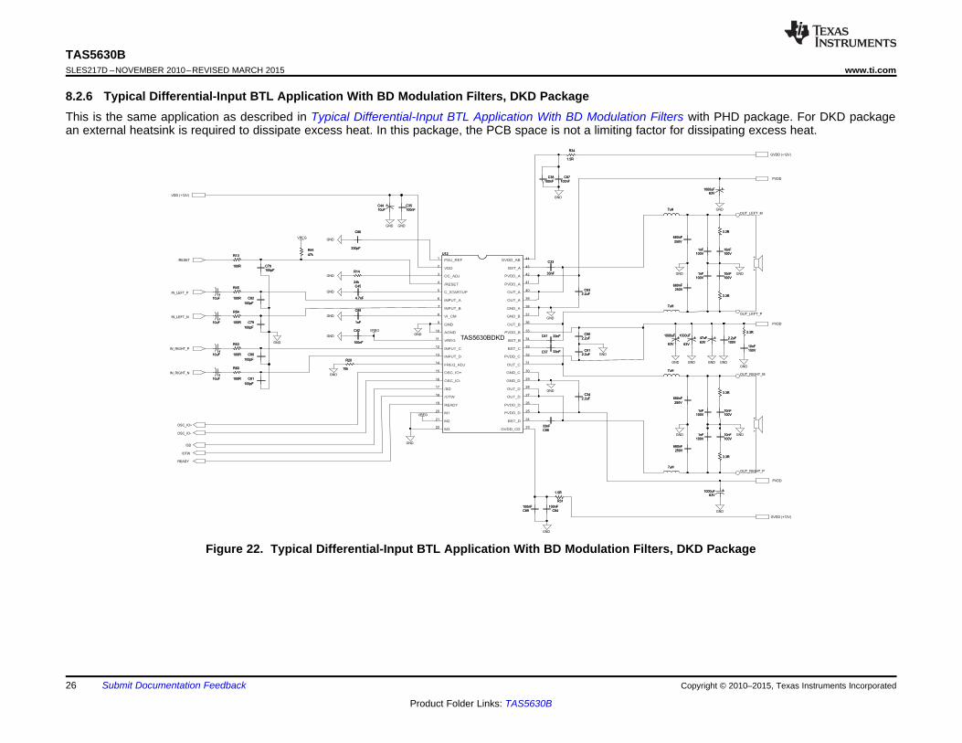
IN_LEFT_N
IN_LEFT_P
IN_RIGHT_N
IN_RIGHT_P
/SD
/OTW
READY
GVDD (+12V)
PVDD
OSC_IO+
OSC_IO-
GVDD (+12V)
VDD (+12V)
PVDD
PVDD
/RESET
GNDGND
GND
GND GND
GNDGND
GND
GND
GNDGND
GND
GND
GND
GND
GND
VREG
GND
GND
GND
GND
GND
GND
GNDVREG
GND
GND
VREG
GND
GND
OUT_LEFT_P
OUT_LEFT_M
OUT_RIGHT_P
OUT_RIGHT_M
+
-
+
-1
2
3
4
5
6
7
8
9
10
11
12
13
14
15
16
17
18
19
20
21
22
33
34
35
36
37
38
39
40
41
42
43
44
23
24
25
26
27
28
29
30
31
32
C8833nFC8833nF
C85
1nF
C85
1nF
3.3R3.3R
7uH7uH
2.2uF
100V2.2uF
100V
C41 33nFC41 33nF
680nF
250V680nF
250V
10nF100V10nF100V
3.3R3.3R
10uF10uF
10uF10uF
10uF10uF
R45
100R
R45
100R
10nF100V10nF100V
1000uF
63V
1000uF
63V
C81
100pF
C81
100pF
C78100pFC78100pF
C37 33nFC37 33nF
C79
100pF
C79
100pF
R14
24k
R14
24k
C35100nFC35100nF
R44
47k
R44
47k
C38
100nFC38
100nF
C342.2uF
C342.2uF
R34
1.5R
R34
1.5R
C80
100pF
C80
100pF
U12U12
TAS5630BDKD
PSU_REF
VDD
OC_ADJ
/RESET
C_STARTUP
INPUT_A
INPUT_B
VI_CM
GND
AGND
VREG
INPUT_C
INPUT_D
FREQ_ADJ
OSC_IO+
OSC_IO-
/OTW OUT_D
OUT_D
GND_D
GND_C
OUT_C
PVDD_C
BST_C
BST_B
PVDD_B
OUT_B
GND_B
GND_A
OUT_A
OUT_A
/SD
GVDD_AB
BST_A
PVDD_A
PVDD_A
M1
M2
M3 GVDD_CD
BST_D
PVDD_D
READY PVDD_D
C33
33nF
C33
33nF
680nF
250V
680nF
250V
C912.2uF
C912.2uF
7uH7uH
R13
100R
R13
100R
C84100nF
C84100nF
3.3R3.3R
10nF100V10nF100V
C87
100nFC87
100nF
1nF100V
1nF100V
3.3R3.3R
R60
100R
R60
100R
680nF
250V680nF
250V
1000uF63V
1000uF63V
3.3R3.3R
C42
100nF
C42
100nF
C902.2uF
C902.2uF
R20
10k
R20
10k
C4410uFC4410uF
7uH7uH
680nF
250V
680nF
250V
10uF10uF
C832.2uF
C832.2uF
1000uF
63V
1000uF
63V
C89100nFC89100nF
R31
1.5R
R31
1.5R 1000uF63V
1000uF63V
C45
4.7nF
C45
4.7nF
10nF100V10nF100V
C86
330pF
C86
330pF 10nF100V10nF100V
47uF
63V
47uF
63VR53
100R
R53
100R
1nF100V
1nF100V
C82
100pF
C82
100pF
7uH7uH
1nF100V
1nF100V
1nF100V
1nF100V
R54
100R
R54
100R
TAS5630BSLES217D –NOVEMBER 2010–REVISED MARCH 2015 www.ti.com
8.2.6 Typical Differential-Input BTL Application With BD Modulation Filters, DKD PackageThis is the same application as described in Typical Differential-Input BTL Application With BD Modulation Filters with PHD package. For DKD packagean external heatsink is required to dissipate excess heat. In this package, the PCB space is not a limiting factor for dissipating excess heat.
Figure 22. Typical Differential-Input BTL Application With BD Modulation Filters, DKD Package
26 Submit Documentation Feedback Copyright © 2010–2015, Texas Instruments Incorporated
Product Folder Links: TAS5630B
TAS5630Bwww.ti.com SLES217D –NOVEMBER 2010–REVISED MARCH 2015
9 Power Supply RecommendationsAbsolute Maximum Ratings discusses most of the requirements on TAS5630B power supply. There are a fewmore important guidelines that should be considered. The most important parameters are the absolute maximumrating on PVDD pins, bootstrap pins and output pins. Over stress the device with higher that maximum voltagerating may shorten device lifetime operation and even cause device damage. Be sure that the specifications insection 6 are observed. For best audio performance, low ESR bulk capacitors are recommended. Depending onthe application 470-µF capacitor or higher should be used. As always, decoupling capacitors must be placed nomore than 1 mm from the power supply pins. If PCB space is not allowed for close decoupling capacitorplacement, the decoupling capacitors can be placed on the back side of the device with vias. However, it stillneeds to be right below the pins.
10 Layout
10.1 Layout GuidelinesUse an unbroken ground plane to have a good low-impedance and -inductance return path to the power supplyfor power and audio signals. PCB layout, audio performance and EMI are linked closely together. The circuitcontains high, fast-switching currents; therefore, care must be taken to prevent damaging voltage spikes. Routingof the audio input should be kept short and together with the accompanying audio-source ground. A local groundarea underneath the device is important to keep solid to minimize ground bounce. It is always good practice tofollow the EVM layout as a guideline.
Netlist for this printed circuit board is generated from the schematic in Figure 18.
Copyright © 2010–2015, Texas Instruments Incorporated Submit Documentation Feedback 27
Product Folder Links: TAS5630B
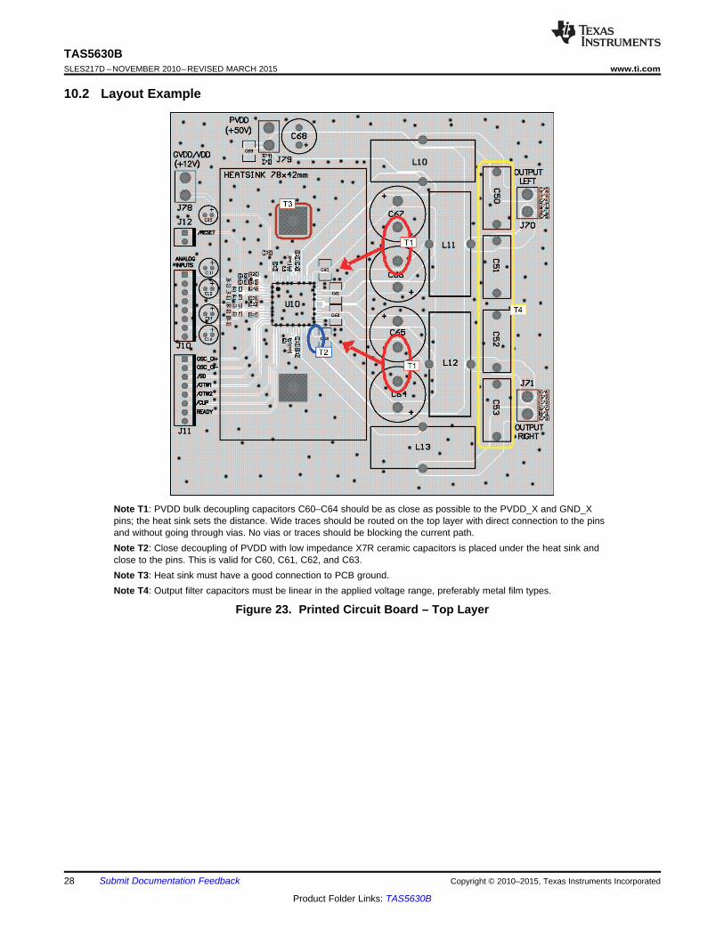
TAS5630BSLES217D –NOVEMBER 2010–REVISED MARCH 2015 www.ti.com
10.2 Layout Example
Note T1: PVDD bulk decoupling capacitors C60–C64 should be as close as possible to the PVDD_X and GND_Xpins; the heat sink sets the distance. Wide traces should be routed on the top layer with direct connection to the pinsand without going through vias. No vias or traces should be blocking the current path.Note T2: Close decoupling of PVDD with low impedance X7R ceramic capacitors is placed under the heat sink andclose to the pins. This is valid for C60, C61, C62, and C63.Note T3: Heat sink must have a good connection to PCB ground.Note T4: Output filter capacitors must be linear in the applied voltage range, preferably metal film types.
Figure 23. Printed Circuit Board – Top Layer
28 Submit Documentation Feedback Copyright © 2010–2015, Texas Instruments Incorporated
Product Folder Links: TAS5630B

TAS5630Bwww.ti.com SLES217D –NOVEMBER 2010–REVISED MARCH 2015
Layout Example (continued)
Note B1: It is important to have a direct-low impedance return path for high current back to the power supply. Keepimpedance low from top to bottom side of PCB through a lot of ground vias.Note B2: Bootstrap low-impedance X7R ceramic capacitors placed on bottom side provide a short, low-inductancecurrent loop.Note B3: Return currents from bulk capacitors and output filter capacitors
Figure 24. Printed Circuit Board – Bottom Layer
Copyright © 2010–2015, Texas Instruments Incorporated Submit Documentation Feedback 29
Product Folder Links: TAS5630B

TAS5630BSLES217D –NOVEMBER 2010–REVISED MARCH 2015 www.ti.com
11 Device and Documentation Support
11.1 TrademarksPurePath is a trademark of Texas Instruments.All other trademarks are the property of their respective owners.
11.2 Electrostatic Discharge CautionThese devices have limited built-in ESD protection. The leads should be shorted together or the device placed in conductive foamduring storage or handling to prevent electrostatic damage to the MOS gates.
11.3 GlossarySLYZ022 — TI Glossary.
This glossary lists and explains terms, acronyms, and definitions.
12 Mechanical, Packaging, and Orderable InformationThe following pages include mechanical, packaging, and orderable information. This information is the mostcurrent data available for the designated devices. This data is subject to change without notice and revision ofthis document. For browser-based versions of this data sheet, refer to the left-hand navigation.
30 Submit Documentation Feedback Copyright © 2010–2015, Texas Instruments Incorporated
Product Folder Links: TAS5630B

TAPE AND REEL INFORMATION
*All dimensions are nominal
Device PackageType
PackageDrawing
Pins SPQ ReelDiameter
(mm)
ReelWidth
W1 (mm)
A0(mm)
B0(mm)
K0(mm)
P1(mm)
W(mm)
Pin1Quadrant
TAS5630BDKDR HSSOP DKD 44 500 330.0 24.4 14.7 16.4 4.0 20.0 24.0 Q1
PACKAGE MATERIALS INFORMATION
www.ti.com 5-Jan-2022
Pack Materials-Page 1

*All dimensions are nominal
Device Package Type Package Drawing Pins SPQ Length (mm) Width (mm) Height (mm)
TAS5630BDKDR HSSOP DKD 44 500 350.0 350.0 43.0
PACKAGE MATERIALS INFORMATION
www.ti.com 5-Jan-2022
Pack Materials-Page 2
TUBE
*All dimensions are nominal
Device Package Name Package Type Pins SPQ L (mm) W (mm) T (µm) B (mm)
TAS5630BDKD DKD HSSOP 44 29 508 18.54 6350 8.13
PACKAGE MATERIALS INFORMATION
www.ti.com 5-Jan-2022
Pack Materials-Page 3

TRAY
Chamfer on Tray corner indicates Pin 1 orientation of packed units.
*All dimensions are nominal
Device PackageName
PackageType
Pins SPQ Unit arraymatrix
Maxtemperature
(°C)
L (mm) W(mm)
K0(µm)
P1(mm)
CL(mm)
CW(mm)
TAS5630BPHD PHD HTQFP 64 90 6 X 15 150 315 135.9 7620 20.3 15.4 15.45
PACKAGE MATERIALS INFORMATION
www.ti.com 5-Jan-2022
Pack Materials-Page 4

www.ti.com
GENERIC PACKAGE VIEW
This image is a representation of the package family, actual package may vary.Refer to the product data sheet for package details.
HTQFP - 1.20 mm max heightPHD 64QUAD FLATPACK14 x 14, 0.8 mm pitch
4224851/A


IMPORTANT NOTICE AND DISCLAIMERTI PROVIDES TECHNICAL AND RELIABILITY DATA (INCLUDING DATA SHEETS), DESIGN RESOURCES (INCLUDING REFERENCE DESIGNS), APPLICATION OR OTHER DESIGN ADVICE, WEB TOOLS, SAFETY INFORMATION, AND OTHER RESOURCES “AS IS” AND WITH ALL FAULTS, AND DISCLAIMS ALL WARRANTIES, EXPRESS AND IMPLIED, INCLUDING WITHOUT LIMITATION ANY IMPLIED WARRANTIES OF MERCHANTABILITY, FITNESS FOR A PARTICULAR PURPOSE OR NON-INFRINGEMENT OF THIRD PARTY INTELLECTUAL PROPERTY RIGHTS.These resources are intended for skilled developers designing with TI products. You are solely responsible for (1) selecting the appropriate TI products for your application, (2) designing, validating and testing your application, and (3) ensuring your application meets applicable standards, and any other safety, security, regulatory or other requirements.These resources are subject to change without notice. TI grants you permission to use these resources only for development of an application that uses the TI products described in the resource. Other reproduction and display of these resources is prohibited. No license is granted to any other TI intellectual property right or to any third party intellectual property right. TI disclaims responsibility for, and you will fully indemnify TI and its representatives against, any claims, damages, costs, losses, and liabilities arising out of your use of these resources.TI’s products are provided subject to TI’s Terms of Sale or other applicable terms available either on ti.com or provided in conjunction with such TI products. TI’s provision of these resources does not expand or otherwise alter TI’s applicable warranties or warranty disclaimers for TI products.TI objects to and rejects any additional or different terms you may have proposed. IMPORTANT NOTICE
Mailing Address: Texas Instruments, Post Office Box 655303, Dallas, Texas 75265Copyright © 2022, Texas Instruments Incorporated
Related Documents


