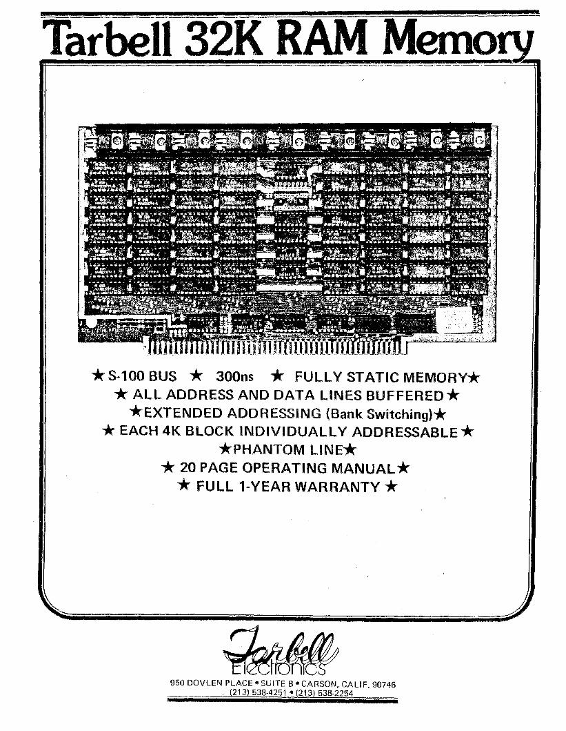
Tarbell 32K RAM * 300ns * FULLYSTATICMEMORV* * ALL ADDRESS AND DATA LINES BUFFEREO* *EXTENDED ADDRESSING (Bank Switching)* * EACH 4K BLOCK INDIVIDUALL V ADDRESSABLE * *PHANTOM LINE* * 20 PAGE OPERATING MANUAL * * FULL WARRANTV * 950 DOVLEN PLACE· SUITE B· CARSON, CALIF. 90746 . (213) 538-4251 • (213) 538-2254 -

Welcome message from author
This document is posted to help you gain knowledge. Please leave a comment to let me know what you think about it! Share it to your friends and learn new things together.
Transcript
Tarbell 32K RAM Mem~
*S~100BUS * 300ns * FULLYSTATICMEMORV** ALL ADDRESS AND DATA LINES BUFFEREO**EXTENDED ADDRESSING (Bank Switching)** EACH 4K BLOCK INDIVIDUALLV ADDRESSABLE *
*PHANTOM LINE** 20 PAGE OPERATING MANUAL** FULL 1~VEAR WARRANTV *
950 DOVLEN PLACE· SUITE B· CARSON, CALIF. 90746. (213) 538-4251 • (213) 538-2254-

r
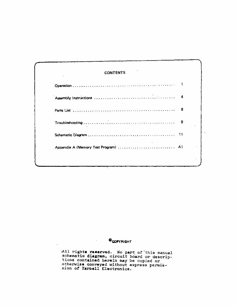
CONTENTS
Operation, ....•.. , ..•................ , .. , ,., .
Assemblv Instructions .... , ..... ",., .. ,", , .. ' .. , , , . , . , . , , ...
Parts List ......•..... , , ,.,., .. " .
Troubleshooting ••............•......... , , . , ... , .. , . , . , . , . ,
Schematic Diagram .•• , •••. , •• , ••......•.....•. , . , , , , .
4
8
9
11
Appendix A (Memory Test Program) •.•.. , ..• , ... , .... , . , ... , ,. A1
f)QOPVAIQHT
\AIl right. r8 ••rved. No part of'this manualschematic diagram. circuit board or descriptions contained herein may be copied orotherwise oonveyed without express permission of T~bell Electronics.
OPERATION
Introduction:
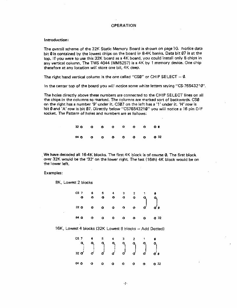
The overall scheme of the 32K Static Memory Board is shown on page 10. Notice databit 0 is contained by the lowest chips on the board in 8-4K banks. Data bit 07 is at thetop. If you were to use this 32K board as a 4K board, you could install only 8 chips inany vertical column. The TMS 4044 (MM5257) is a 4K by 1 memory device. One chiptherefore at any location will store one bit, 4K deep.
The right hand vertical column is the one called "CS0" or CHIP SELECT - 0.
In the center top of the board you will notice some white letters saying "CS-76543210"'.
The holes directly above these numbers are connected to the CHIP SELECT lines on allthe chips in the columns so marked. The columns are marked sort of backwards. CS0on the right has a number '9' under it. CS07 on the left has a '1' under it. 'H' row isbit 0and 'A' row is bit 07. Directly below "CS76543210" you will notice a 16 pin DIPsocket. The Pattern of holes and numbers are as follows:
320
640
o
o
o
o
o
o
o
o
o
o
o
o
o.
o 32
_We have decoded all 16-4K blocks. The first 4K block is of course 0. The first blockover 32K would be the '32' on the lower right. The last (16th) 4K block would be onthe lower left.
Examples:
8K, Lowest 2 blocks
CS7 6 5 4 3 2 II0 0 0 0 0 0 ) ).
320 0 0 0 0 0
640 0 0 0 0 0 0 o 32
16K, Lowest 4 blocks (32K Lowest 8 blocks - Add Dotted)
CS 7 6 5 4 3 2 IIQ, ~ ~ ~
J J J J.. •: ,
d,
32 a' d •d
640 0 0 0 0 0 0 o 32

16K, Lowest 4 blocks but chips in every other column
CS1o
320
640 o o o o o o 32
16K, From 32K to 48K (Chips in right side of board)
CS 1o
320
640
6
o
o
o
5o
o
o
4
o
o
o
The placement of the chips on the board and corresponding decoded bank assignmentare completely flexible. You could cross all the wires up and have any 4K section anywhere you wish. Try to think of the 32K board as 8 conventional 4K boards, all invertical columns starting from right to left. Since there are 16-4K banks available foruse in a $.100 computer, you must decide where your 8 will go.
More Examples:
~Q..~
~ .2... iN l"ll "" <C !'" IlIlI CD .li:= = = = c c c = ..e e e e e e e e ..::l ::l ::l ::l ::l ::l ::l .= a:Q Q Q Q Q Q Q Q a..t.l t.l t.l t.l t.l (.,) t.l t.l .=
CS1 El 5 3:;
4 :2 1 II Q"
0 0 0 0 0 0 0 0 0
::.c ::.c ~ ::.c ::.c ::.c ::.c ::.cN CD .,. Q <l:I iN l:D ""l"ll ('\I N ('\I ... ...I I ! I I I I
::.c ::.c ::.c ::.c ::.c ::.c ::.cIlIlI .... Q u:I l'I l:D .... •N ('II iN ... ...
320 0 0 0 0 0 0 00
640 0 0 0 0 0 0 032::.c ::.c ::.c ::.c ::.c' ::.c ::.c ::.c;2; fi :8 N CD "" Q u:I
10 "" "" "" l"llI I I I I I I I
::.c ::.c ::.c ::.c ::.c ::.c ::.c ::.c~ u:I N CD ., Q u:I ('II
10 10 "" '!II" "" (') l"ll
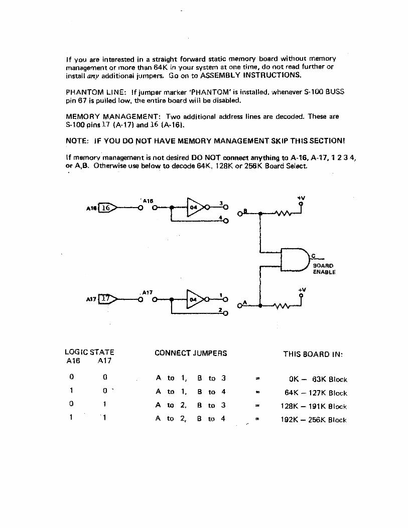
If you are interested in a straight forward static memory board without memorymanagement or more than 64K in your system at one time, do not read further orinstall any additional jumpers. Go on to ASSEMBLY INSTRUCTIONS.
PHANTOM LINE: If jumper marker 'PHANTOM' is installed, whenever $-100 BUSSpin 67 is pulled low, the entire board will be disabled.
MEMORY MANAGEMENT: Two additional address lines are decoded. These areS-l00 pinsl? (A-H) and 16 (A-16).
NOTE: IF YOU DO NOT HAVE MEMORY MANAGEMENT SKIP THIS SECTIONI
If memory management is not desired DO NOT connect anything to A-16, A-17, 1 234,or A,B. Otherwise use below to decode 64K, 128K or 256K Board Select.
~Al1~M7~ " .. 2
A
+v
LOGIC STATE CONNECT JUMPERS THIS BOARD IN:A16 A17
0 0 A to 1, B to 3 ... OK - 63K Block
1 o . A to 1, B to 4 := 64K - 127K Block
0 1 A to 2, B to 3 == l28K - 191 K Block
1 '1 A to 2, B to 4 "" 192K - 256K Block

ASSEMBLY INSTRUCTIONS
1. Open bag of .1 mfd capacitors and straighten leads.
2. Refer to drawing No.1. Install all .1 capacitors at locations shown.
3. Turn board and solder all leads.
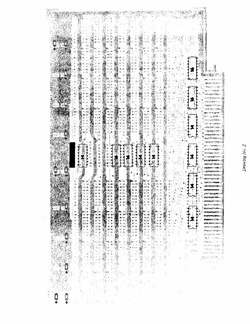
4, locate capacitors C2 in kit. BE CAREFUL. TO OBSERVE POLARITYIInstall each capacitor at locations shown on drawing No.2 beforesoldering, go back and check against drawing for incorrectly polarizedcapacitors. Most boards returned for repair have contained errors in polarity.What happens is that a backward capacitor blows the regu lator, which thf,mzapps a whole column of memory chipsl (booooll)
5. ( Install 5 resistors, 1K value at places shown on drawing No.1. Solder atthis time.
6. ( ) Locate all 64 18 pin sockets. Put them into the board one column at a time.Hold them in place with a piece of cardboard and flip board to back side.Solder or bend 2 corner pins of each chip (Le. pins 8 & 16). Then go on tonext column. To complete soldering go down a row after placing board ontable long side up. This seems to be the fastest. After soldering entire board,inspect under strong light for solder splashes or webs.
7. ( ) Locate special 16 pin socket that has molded circular receptacles. Install thissocket at the decoded address po~ition.·
:1....: : : :......._:,.;;,.._....: :__-.;..:1:2
8. ( ) Refer to drawing No.2. Install remaining 14 and 16 pin sockets. Firstput a small piece of black "tape over feed through holes at top center ofboard.
9. ( ) Then mount heat sink in place using only outer 2 regulator screw holes.Make sure that the heat sink is positioned perfectly over all capacitors andother screw holes. Spend some time here and do this right. It's not impossibleto misallgn the sink and short the +6 on a capacitor lead. After settingeverything up straight, carefully mount center 7 regulators in place as perboard photo. Don't forget to apply a small dab of white heat sink compoundto the underside of each regulator before bolting it down. After insideregulators are done, r~move outside screws and do those two too. (1)

10. ( ) Time now to start buzzing out the shorts. The most important ones are the+8 to +5 possibil ities. Pin 1 of S-l 00 connector at lower left is +8. Make sureas you go from left to right across board that no pin 18 on any column has alow resistance path to +8, A buzz box can be used if a meter is not available.Address Iines can be checked if necessary as well as data. We suggest removing all boards from your computer before plugging in the memoryboard. Check output from +5 regulators (the lower pin) on all regulators.
11. ( ) Install all 16 and 14 pin chips. *lnstall row of round chip select pins at 'CS'as per drawing No. ( 1 ). The right most pin is a pull up resistor that maybe tied to any unconnected bank of chips to insure that they do not intermittently 'select' themselves on noise.
NOTE: ON ALL 16K BOARDS, ALTERNATE UNUSED es's MUST BEPULLED UP!
12. ( ) Install a single column of 8 memory chips. Use the correct 'CS' for thecolumn you have filled. They correspond to the physical location on theboard of the columns except that the right mast 'CS' pin is a pullup and ismarked '8D'. For example if you had filled the right most column withchips, CS line 0 would access that column. If you would like to place that4K bank at 48K+ for the purpose of test, make a jumper from CS 0 to thefourth Din on the bank decode IC sacket.
CS7
o
320
640
8o
o
o
5
o
o
o
4
o
o
3o
o
o
2o
o
o
1o
o
o
'"
011
032
bdo (pullup)
13. ( ) Continue filling columns and testing with whatever memory test you have.We recommend that if you are planning only 16K of memory chips fora while, to use every ather column to maximize cooling. A fully stuffed 32Kboard MUST have some farced cooling (at least 10 cfm) passing over thechip side of the board. Constantly check the board heat during the first15 minutes of operation. An undercooled board will shaw data errors withinthe first hour of operation. These are caused by memory slowing dawn as itheats up. Usually no permanent damage results. Very hot boards do seem tocrash chips more than coal ones though. Any reasonable cooling will allow2 fully stuffed 32K boards to be run slat to slat. 16K (half stuffed) can berun with convection cool ing. A fan never hurts though!
•Refer to finished board photo for Ie location.
-5-

'1\~~~i~'''';'";::: Al71 ,'~',.,''', ",t, ;", ::)
0",w """",,..,.:{.:~,.'~
'/ -y:JZ}';;:,',(1~8j;~1',!\~';i· ~ N{
,; ~ > ~tE ~~,{f.'.1;~:"'N1tl"(t~{~_l~'~'!iw" "~;~
., 4< :''fj~.:",-,~,'tji''''C';1'~:'fil'::''1r-'''':;~~
:. .}:tl"M
'. lilt' " '"''ir,''Y''''' :"~_:~"'F! ",'. . '.: ',''',~rl,,.,~m_,,,,"-i: ~ ~ '...: ~ .
'-.)"'6
'@"'" "",·1(,,"1""'·''.''''''
'.'",',..~.•._'.•..,..•.. ,. ,---i, _J---.", . ,I' i ~_''''M!'-'~), ,j' ,r r ; ~ ,, "',' ",' :" -.",'
'~Gl~=I, I ,
• ",I ~~~--.... ~. i""'''''~~.."._.,f1l;!§.:1., / _.W'''''lI'II-.~~
!, " """""'-~--~" I: :" ... '" :~lmr~1'fJjj#r1.'1~\r.:~--;1
:';'i i f2':;~':;:~t;:~~,.:.it·-:;g:;';':,~~,~:Af
D a Il Q a IJ "[1 £1 irr 0 £J 11 D. DOll
11" -
"'llI<\1l ....... Ill!. ... _ .. "!-.!e,~'!It.t_ "'"~~ ... "'J'" " ....... ,,",<11"' .... Ill" 4l' "" • .!. ... !..,.!...~'I' ..! ""." _II '!-.. "'...!" ",t !J~'!' "'!l~ !!"'_~' "..
III .. f' ..... II " , ... " It "':'" ..... ., .. " .. " " " .. f ~ ~ " " ..". <l._~ ~ .. "'. ~ , " .... '" .... " " .. , .. .. '" .. '" ......, t .. '!' .... " " '" " ..
_ .. , _ _ '" .. '" '" ':' .. ,.... ' 'I .. .. " , .. .. ~ .. 1''' ""!!,..~lllol!<'I'~~1Il!l 1I .. <t~ ", t" "" "", .. ,, "'1'" ~ .. "'.! ~" ..
~ .... '" , .. .. ., ~ " " " , .. " , " • .. oil It f '!' ~...... ..,.. " t .. II< '" ~ .. '" " .. '" t " "It ..
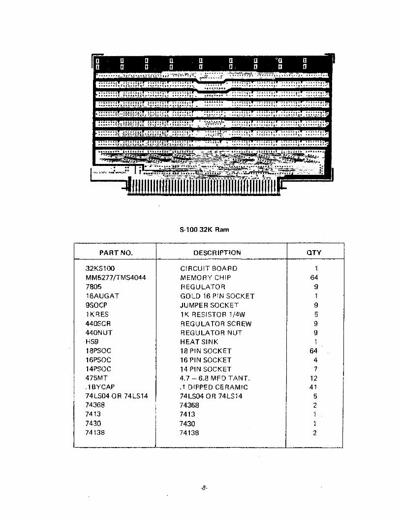
S-10032K Ram
PART NO, DESCRIPTION OTY
32KS100 CIRCUIT BOARD 1MM5277/TMS4044 MEMORY CHIP 647805 REGULATOR 916AUGAT GOLD 16 PIN SOCKET 19S0CP JUMPE R SOCKET 91KRES 1K RESISTOR 1/4W 5440SCR REGULATOR SCREW 9440NUT REGULATOR NUT 9HS9 HEAT SINK 118PSOC 18 PIN SOCKET 6416PSOC 16 PIN SOCKET 414PSOC 14 PIN SOCKET 7475MT 4.7 - 6.8 MFD TANT, 12.1 BYCAP ,1 DIPPED CERAMIC 4174LS04 OR 74LS14 74LS04 OR 74LS14 574368 74368 27413 7413 17430 1430 174138 74138 2
-8-
TROUBLESHOOTING
1. Most troubles occurring immediately after construction are shorts. Close visualinspection is much faster than logical circuit tracing for this type of problem.
Open circuits caused by over etching of the p.c. board or bad soldering are by farthe most difficult problems to locate. Memory tests run on boards with openaddress lines give strange results that often do not point to tile real problem.A general rule of thumb is that if the problem is random and somewhat unpredictable, an open is probably at fault. If the problem is very predictable and regular,a short or bad chip is at fault.
A 'Buzz Box' is an absolutely indispensable tool in checking memory boards.You do not have to look up from your work each time to verify continuity.The many circuit traces on a memory board are a problem by themselves withouthaving to lose your place each time you :~ave to look up to a m!;!ter face.
2. If the memory board has been in service for some time and a problem with it issuspected, a memory test should be run. The Rasmussen test for diseased memoryis a factory test designed to display the most common problems first and the mostuncommon ones last. The test never finishes by itself. The operator may terminateit by pressing the space bar at any time.
Generally memory chip failures will be found within five seconds. The test takesabout three minutes to run all phases in a 32K board. The test falls into a randomnumbers test at the end of the first phase and will stay there until a space bar isentered.
When initializing the test for a 32K board addressed at 0000, the correct answers tothe address prompt entry would be 0000 and 7FFF. The test will do the following:
STUCK BIT: Fills test area with FF's and checks for FF'sFills test area with 00's and checks for 00's
BIT SHORTED: Rotates a bit from LSB to MSB filling tested memoryeach time, checking one bit at a time
ADDRESS SHORTED: Fills all memory with 55 Hex then writes an AA Hexat 0000 (or the lowest address tested). It then teststhe rest of memory for 55's. Then it clears locationof the AA and writes it into 0001. Then 0002, 0004,0008, etc. setting a new address bit high each timeand testing all of memory. If any address bit is shortedto another, the test will find an AA in another locationthan the place it wrote one. This test takes the mosttime and is run last.
·9-
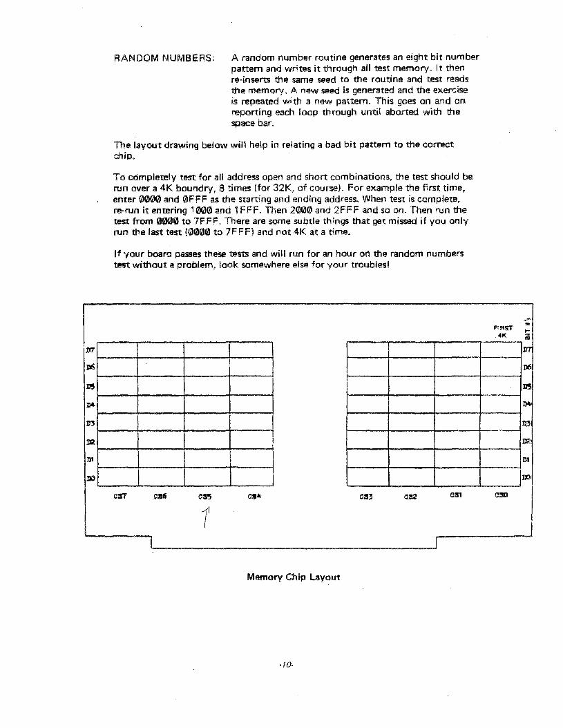
RANDOM NUMBERS: A random number routine generates an eight bit numberpattern and writes it through all test memory. It thenre-inserts the same seed to the routine and test readsthe memory. A new seed is generated and the exerciseis repeated with a new pattern. This goes on and allreporting each loop through until aborted with thespace bar.
The lavout drawing below will help in relating a bad bit pattern to the correctchip.
To completely test for ail address open and short combinations, the test should berun over a 4K boundry, 8 times (for 32K, of course). For example the first time,enter 0000 and 0FFF as the starting and ending address. When test is complete,re--run it entering 1000 and 1FFF. Then 2000 and 2FFF and so on. Then run thetest from 0000 to 7FFF. There are some subtle things that get missed if you onlyrun the last test (0000 to 7F FF) and not 4K at a time.
If your boara passes these tests and will run for an hour on the random numberstest without a problem, look somewhere else for your troublesl
....FIRST
."~
41( ;;
111 1111J)6 ll6
1I5 1I5
:tl4 1]]4
D' II'112 I II2
])1 D1
1X'l DO
c:rr CM CS5 ca4 as, Cl!2 CSt aso
1j
Memory Chip layout
·10-


1--3'. 0---1'.
(, ,..
---
I
~i
!ii
III
,II I
/
,
I
1O 2.0 3D
~ f= ,
= ::~.. ~... f.-..=TiOI
1'\"" 1"l!
\~"'''10""
!l0l0lT
1'10 e-
.. ,.,
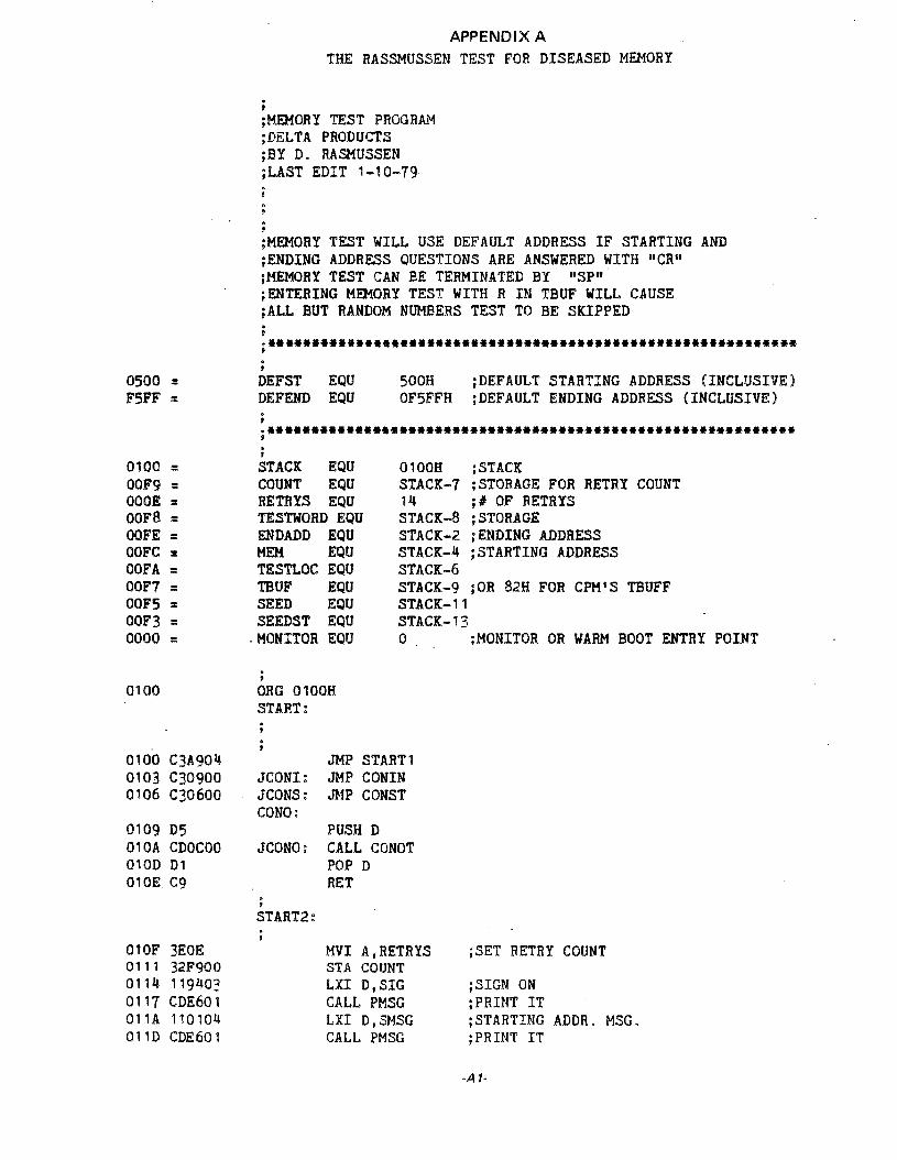
APPENDIX ATHE RASSMUSSEN TEST FOR DISEASED MEMORY
·,jMEMORY TEST PROGRAl"!;DELTA PRODUCTSJBY D. RASMUSSENjLAST EDIT 1-10-79
jMEMORY TEST WILL USE DEFAULT ADDRESS IF STARTING ANDjENDING ADDRESS QUESTIONS ARE ANSWERED WITH "CR"jMEMORY TEST CAN BE TERMINATED BY "SP"jENTERING MEMORY TEST WITH R IN TBUF WILL CAUSEjALL BUT RANDOM NUMBERS TEST TO BE SKIPPED·,•••••••••••••••••••••••••••••••••••••••••••••••••••••••••••••,
0500 ::FSFF ::
·,DEFST EQUDEFEND EQU
500H jDEFAULT STARTING ADDRESS (INCLUSIVE)OF5FFH jDEFAULT ENDING ADDRESS (INCLUSIVE)
·,.•••••••••••••••••••••••*•••••••••••**••••••••••••••*••••••••,·,
0100 :: STACK EQU 0100H ;STACK00F9 :: COUNT EQU STACK-7 jSTORAGE FOR RETRY COUNTOOOE :: RETRYS EQU 14 jl OF RETRIS00F8 :: TESTWORD EQU STACK-8 ;STORAGEOOFE :: ENDADD EQU STACK-2 jENDING ADDRESSOOFC :: HEM EQU STACK-4 jSTARTING ADDRESSOOFA :: TESTLOC EQU STACK-600F7 :: mUF EQU STACK-g JOR 82H FOR CPM'S mUFFOOFS == SEED EQU STACK-ll00F3 :: SEEDST EQU STACK-130000 :: . MONITOR EQU 0 jMONITOR OR WARM BOOT ENTRY POINT
·,0100 ORG 0100H
START:
0100 C3A9040103 C309000106 C30600
0109 05010A CDOCOO0100 Dl010E cg
010F 3EOE0111 32F9000114 11940::0111 COE601011A 110104011D COE60 1
JCONI:JCONS:CONO:
JCONO:
·,START2:
JMP STARTlJMP CONINJMP CONST
PUSH DCALL CONOTPOP 0RET
MVI A,RETRYSSTA COUNTLXI D,SIGCALL PMSGLXI D,SMSGCALL PMSG
;SET RETRY COUNT
jSIGN ONjPRINT ITjSTARTING ADDR. MSG.jPRINT IT
·A 1-

0120 CD00030123 022E010126 2100050129 £5012A CDOA01012D E1
012E 22FCOC0131 1123040134 CDE6010131 CD0003013A 024501013D 21FFF50140 E50141 CDDA010144 El
0145 22FEOO
0148 3AF100014B FE520140 CA40030150 115C040153 CDE6010156 06FF0158 CDF101015B CD0802015E 06000160 CDF1010163 CD08020166 116D040169 CDE601016C 3E01
CALL GETADDmc L.DSTlL.XI H,DEFSTPUSH HCALL PHLPOP H
t.DSTl :SHLD MEML.XI D,EMSGCALL PMSGCALL GETADDJUC L.D5T2L.XI H, DEFF-NDPUSH HCALL PHLPOP H
t.DST2:SHLD ENDADD
RESTART:t.DA TaUFCPI 'R'JZ RNDWL.XI D, TEST 1CALL PMSGMYI B,OFFHCALL TES.TWCALL TESTRMYI B,OCALL TESTWCALL TESTRLXI D,TEST3CALL PMSGMil A,l
jGET·STARTING ADDR FROM CONINjFLAG = 0 THEN ENTRY WAS CR;GET DEFULT STARTING ADDR.
jPRIN~ DEFAULT ADDRESS
jSAVE STARTING ADDRESSjENDING ADOR. MSG.
JGET ENDING ADDRESS FROM KEYBOARDjFLAG = a THEN WAS CRjDEFAULT END ADDR HIGH BYTE
jPRINT DEFAULT ADDRESS
jSAVE ENDING ADDRESS
JGET TaUF TO SEE IF RANDOM TEST ONLYiIF R THEN GO DIRECTLY TO RANDOM TESTJGO DO RANDOM NUMBERS
jPRINT TESTiFF TEST START;WRITE TEST BYTEjCHECK TEST BYTEiZEROS .TESTjWRITE TEST BYTE 0;TEST
;PRINT BIT SHORT TEST;ROTATE BIT TEST
016E 41016F CD66020112 D26.£01
LOOP2:MOV B,A JMAKE TEST BYTECALL ROTTST JDO TESTJNC L.00P2 JDONE WITH 8 BITS?.,
jADDRESS LINE TEST
0115 118004 LoXI 0, TEST40178 CDE601 CALL PMSG jPRU1T ADOR. L.INE TEST017B0655 MYI B,558 ;TEST BYTE017D CD1202 CALL ADTEST ;TEST0180 06AA MYI B,OAAH ;TEST BYTE0182 CD7202 CAL.L ADTEST JTEST0185 3E52 MVI A, 'R'0181 32F700 STA TEUF jPUT R IN TeUF - LOOP ON RANDOM TESTalBA C34003 JMPRNDW JOO RANDOM I TEST
DONER:0180 11F103 l.XI O,MSGOK jPOINT AT TEST COMPLEAT MESSAGE
DONEA:0190 COE601 CALL PMSG0193 C34801 JMP RESTART ;START TEST AGAIN WITH OLD PRAMETERS
·A2·

,,PRINT STRING POINTED TO BY D,E
0196 C50197 050198 E50199 F5019A l1A4030190 CDE601OlAO 13OlA 1 3AF900OlA4 FEOEOlA6 CCE60101A9 CDDA01DlAC 50OlAD CD470201BO 780181 CDOC0301B4 Fl01B5 F501B6 570187 CD470201BA Fl01BB eDOC03018E 3AF90001Cl 3D01C2 32F9DO01CS C2D60101 C8 l1CB0301CB eDE60101CE eD00030101 3£0£OlD3 32F900
01D6 El01D7 0101D8 C10109 C9
01DA 54010B CD4702OlOE 55010F CD470201E2 CD2E03OlE5 C9
ERROR:PUSH BPUSH 0PUSH HPUSH PSWLXI D,HSGlCALL PMSGINX DLDA COUNTCPI RETRISCZ PMSGCALL PHLMOV O,BCALL CNVTHOV A,BCALL CNVTBPOP PSWPUSH PSWMOV D,ACALL CNVTPOP PSWCALL CNVTBLDA COUNTOCR ASTA COUNTJNZ MORETLXI D,MSG4CALL PMSGCALL GETADDMVI A,RETRISSTA COUNT
HORET:POP HPOP 0POP BRET.,
,PRINT H,L REGISTER
PHL:MOV D,HCALL CNVTMOV O,LCALL CNVTCALL TABRET
,SAVE ALL REGS.
,PRINT LABLES,PRINT HL REG,GET SHOULD BE DATA,PRINT HEX
;GET WAS DATA;PRINT HEX
;GET ERROR COUNT;ONE LESS;PUT BACK COUNT
;SEE IF STOP OR CONTINUE
;RESET COUNT
,GET ALL REGS. BACK AND CONTINUE TEST
;HAKE ADDRESS OF ERROR ASCII
. ,01E6 1A01E7 87OlEa C801E9 4F01 EA COOgo 101ED 1301 EE C3E60 1
PMSG:LDAX 0ORA ARZMOV C,ACALL CONOINX 0JMP PMSG
-A3-
;GET BYTE TO BE PRINTED;END OF TEXT?
;CONVENTION;GOTO OUTPUT
I
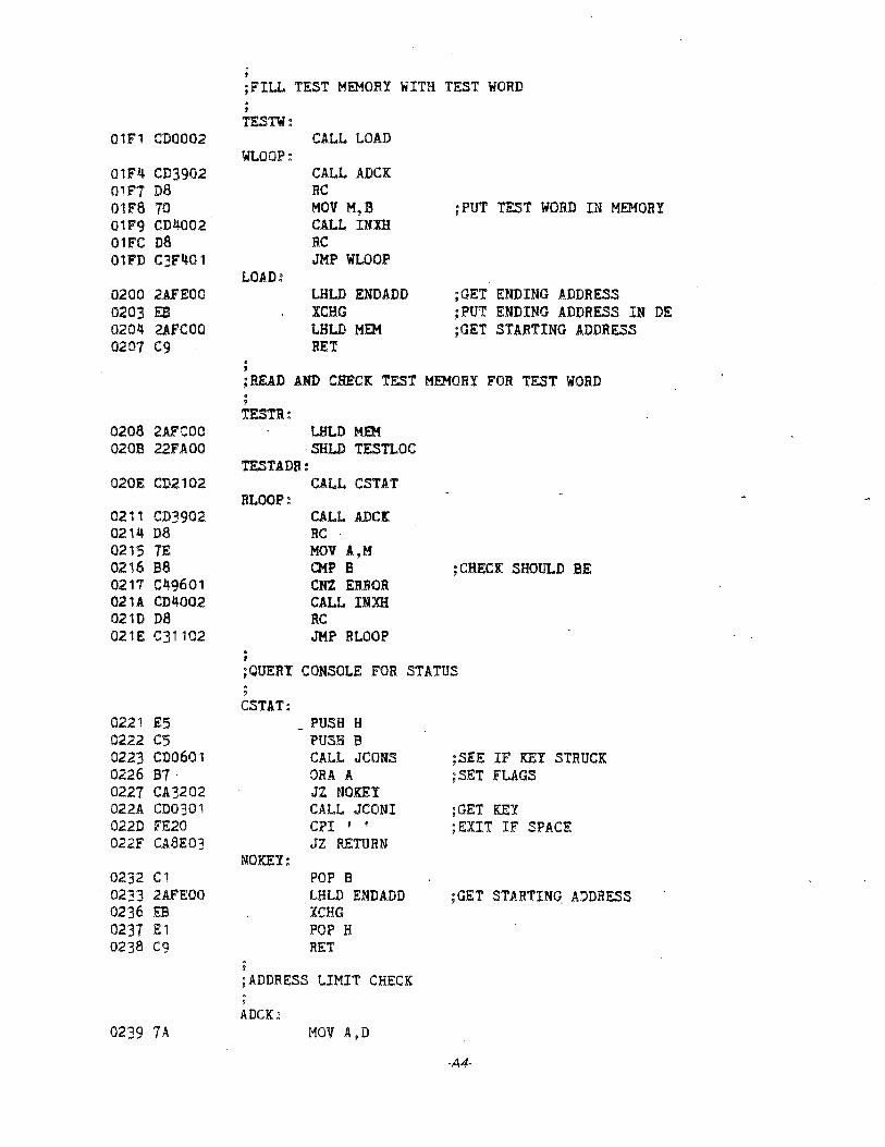
jFILL TEST MEMORY WITH TEST WORD
CALL LOAD
·,TESTW,:
·,; READ AND CHECK TEST MEMORY FOR TEST WORD
01F1 CD0002
01F4 CD390201F7 .0801F8 7001F9 CD400201FC DB01FD C3F40 1
0200 2AF£OO0203 EB020~ 2AFCOO0207 cg
WLOOP:
LOAD:
CALL ADC!RCMOV M,SCALL INXHHCJMP WLOOP
LHLD ENDADDXCHGLHLD HEMRET
;PUT TEST WORD IN MEMORY
;GET ENDING ADDRESSjPUT ENDING ADDRESS IN DE;GET STARTING ADDRESS
0208 2AFCOO020B 22FAOO
020£ CD2102
·,TESTR:
LHLD HEM.SHLD TESTLOC
TESTADR:CALL CSTAT
·I;QUERY CONSOLE FOR STATUS
0211 CD39020214 080215 1£0216 B80211 C49601021A CD4002021.0 08021E C31102
RLOOP:CALL ADCKRCHOV A,MO1PBCNZ ERRORCALL INXHRCJMP BLOOP
;CHECK SHOULD BE
0221 E50222 C50223 C.o06010226B7·0227 CA3202022A CD030102.2.0 FE20022F CA8E03
0232 Cl0233 2AFEOO0236 EB0231 E10238 cg
0239 7A
·,CSTAT:
PUSH HPUSH BC~.LL JCONSOBA AJZ NOKEYCALL JeONICPI I I
JZ RETURNNOKEY:
POP B1..HLD ENDADDXCBGPOP HRET
,jADDRESS LIMIT CHECK,ADCK:
MOV A,D
iSEE IF KEY STRUCK;SET FLAGS
jGET KEY;EXIT IF SPACE
jGET STARTIN~ ADDRESS
·A4-
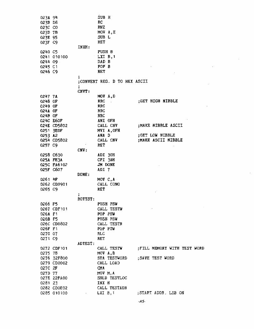
023A 94023B D8023C CO023D 7B023E 95023F cg
0240 C50241 0101000244 09 .0245 Cl0246 C9
SUB HRCRNZMOV A,ESUB LRET
INXH:PUSH BLXI B, 1DAD BPOP BRET.,
jCONVERT REG. D TO HEX ASCII.,CNVT:
JGET HIGH NIBBLE
jMAKE NIBBLE ASCII
JGET LOW NIBBLEjMAKE ASCII NIBBLE
jFILL MEMORY WITH TEST WORD
;SAVE TEST WORD
jSTART ADDR. LSB ON
-A5-
0247 7A HOV A,D0248 OF RRC0249 OF RRC024A OF RRC024B OF RRC024C E60F ANI OFB024E CD5802 CALL CNV0251 3EOF MVI A,OFH0253 A2 ANA D0254 CD5802 CALL CNV0257 cg RET
CNV:0258 C630 ADI 30B025A FE3A CPI 3AB025C FA610.? JM OONE025F C601 ADI 7
DONE:0261 4F MOV C,A .0262 CDOgOl CALL CONO0265 cg RET
;ROTTST:
0266 F5 PUSH PSW0267 CDF101 CALL TESTW026A Fl POP PSW026B F5 PUSH PSW026C CD0802 CALL TESTR026F F1 POP PSW0270 01 RLC0271 cg RET
ADTEST:0272 CDF101 CALL TESTW0275 78 MOV A,B0276 32F800 STA TESTWORD0279 CDOO02 CALL LOAD027C 2F CMA027D 77 MOV M,A027E 22FAOO SHLD TESTLOC0281 23 INX H0282 CDOE02 CALL TESTADR0285 010100 LXI B, 1
LOOP4:0288 2AFCOO LHLD HEM0288 09 DAD B028C D8 RC jROLLED OVER 65K0280 7A MOV A,D JGET TEST ADDR028E 94 SUB B jPAST END?028F D8 HC jKEEP GOING IF NO CARRY0290 C29602 JNZ INXHA0293 7B MOV A,E0294 95 SU8 L0295 D8 RC
INmA:0296 3AF800 LDA TESTWORD0299 C5 PUSH B029A 47 MOV B,A0298 2F CMA ;INVERT BITS029C 77 MOV M,A jWRITE TO TEST MEMORY0290 22FAOO SHLD TESTLOC02AO C04002 CALL IBXH02A3 DAB 102 JC OVERFL02A6 CDOE02 CALL TESTADR jrES!02A9 El POP B02AA 29 DAD H02AB 08 RC02AC 44 MOV B,H02AO 40 MOV C,L02AE C38802 J:HP LOOP4
C'VERFL:028 1 C1 POP B02B2 C9 REt.,
GETBTr:0283 CDD702 CALL CHAR0286 ca HZ0287 FE20 CPI ' , JEXlT IF SPACE02B9 CABE03 JZ RETURN028C CDE502 CALL ATCH028F F2F902 JP REENTER02C2 OF RRC02C3 OF RRC02C4 OF RRC02C5 OF RRC02C6 5F MOV E,A02C7 D5 PUSH D02ca CDD102 CALL CHAR02C5 D1 POP D02CC CAFg02 JZ REENTER02CF CDES02 CALL ATOH0202 F2F902 JP REENTER0205 83 ORA E02D6 C9 RET
CHAR:02D7 CD0301 CALL JCONI020A FEOD CPI ODH02DC 37 STC iSET CARRY FLAG (MAYBE eft)02DD C8 RZ02DE F5 PUSH PSW'
·A6-

02DF 4F MOV C,A02EO CD0901 CALL CONO02E3 Fl POP PSW02E4 C9 RET
ATOH:02E5 D630 SUI 30H02E7 FAF702 JM BAD02EA FEOA CPI OAH02EC F8 ~
02ED D607 SUI 702EF FEOA CPI OAH02Fl FAF702 JM BAD02F4 FE10 CPI 10H02F6 F8 RH
BAD:02F7 AF XRA A iSET ZERO FLAG02F8 C9 RET
REENTER:02F9 E1 POP H iFlX STACK02FA 114504 LXI D,IEMSG02FD CDE601 CALL PMSG
·,iINPUT 4 HEX VALUES FROM CONSOLE·,GETADD:
0300 CDB302 CALL GETBYT0303 DB RC0304 67 HOV H,A0305 E5 PUSH H0306 CDB302 CALL GETBYT0309 E1 POP H030A 6F MOV L,A030B C9 . RET
·,jPRINT REG-A IN BINARY
CNVTB:030C SF HOV E,A iSAVE A030D 1602 HVl D,2 jTWO SPACES030F CD3003 CALL TLOP0312 0602 HVI B,2 iNlBBLE COUNT
PNlBB:0314 1604 . HVl 0,4
ALLaIT:0316 7B MOV A,E jRESTORE A0317 17 RAL0318 5F MOV E,A0319 OE30 MVl C,30H iO031B 022003 JNC ZERO031E OE31 MYl C,31H ; 1
ZERO:0320 CDogOl CALL CONO0323 15 OCR 00324 C216u3 JNZ ALLBIT0327 CD3803 CALL SPACE iPRINT SPACE032A 05 OCR B032B C21403 JNZ PNIBB
·A7·
032E 1604
0330 CD38030'333 150334 C230030337 C9
0338 OE20033A C50338 COOg01033E C1033F cg
TAB:MVI D,4
!LOP:CALL SPACEOCR 0JNZ !LOPRET
SPACE:MVI C,' ,PUSH BCALL CONOPOP BRET
;;RANDOM NUHDER TEST;;WRITE RANDOM NUMBERSRNDW:
0340 1194040343 CDE6010346 2AF5000349 22F300034C 22FAOO034F CDOD02
LXI D,RM~G
CALL PMSGLHLD SEEDSSLD SEEDS!SHLD TESTLOCCALL LOAD
;GE! OLD SEED;SAVE IT FOR LATER
0352 CD1ED30355 700356 CD39020359 CA6003035C 23035D C35203
RNDWL:CALL RNDMOV M,a .CALL ADCKJZ RNDRINI l:IJMP RNDWL.,
;READ AND CHECK RANDOM NUHBERSRNDR:
0360 CD21020363 2AF3000366 22F5000369 CD0002
RNDRL:
CALL CSTATLHLD SEEDSTSHLD SEEnCALL LOAD
;START WITH SAME SEED;PASS SEED TO GENERATOR;GET TEST ADDRESS
036C CD7E03036F 7£0370 B80371 C4960 10374 CD39020377 CA8DOl037A 23037B C36C03
037E E50?7F 2AF5000382 700383 AC0384 470385 070386 6F
CALL RNDMOV A,MCMf 8CNZ ERRORCALL ADCKJZ DONERINX HJMP RNDRL
;GENERATE RANDOM NUMEER FORM SEED,RND:
PUSH HLHLD SEEDMOV A,LXRA HMOV B,ARLCMOV L,A
·A8·
0387 840388 670389 22F500038C E1038D C9 .
038E 31F1000391 C30000
ADD HMOV H,ASHLD SEEDPOP HRET
RETURN:LXI SP,STACK-15 ;FIX STACKJMP MONITOR.,
:MESSAGES.;
0394 OAOD4D454DSIG:03A4 OAOD004C4FMSG1:03AF 202053484F03C8 OAODOO03CB OAOD224352MSG4:03F1.0AOD544553MSGOK:0401 OAOD535441SMSG:0423 OAOD454E44EHSG:0445 OAOD494E50IEMSG:045C OAOD424954TEST1:046D OAOD53484FTEST3:0480 OAOD414444TEST4:0494 OAOD52414ERMSG:
DB OAH,ODH,'MEMORY TEST',ODH,OAH,ODB OAH,ODH,O, 'LOCATION'DB' SHOULD BE WAS'DB OAH,ODH,ODB OAH,ODH, 'nCR" TO CONTINUE TEST "SP" TO STOP ',0DB OAH,ODH,'TEST COMPLETE',ODB OAH,ODH,'STARTING ADDRESS (HEX OR nCR") ',0DB OAH,ODH,'ENDING ADDRESS (HEX OR nCR") ',0DB ·OAH,ODH,'INPUT ERROR RETYPE- ',0DB OAH,ODH,'BIT STUCK TEST',ODB OAH,ODH,'SHORTED BIT TEST',ODB OAH,ODH,'ADDRESS LINE TEST',ODB OAH,ODH,'RANDOM NUMBER TEST',O
04A9 31Fl00
.,•••••••••••••••••••••••••••••••••••••••••••••••••••••••••••••,:;INSEBT CUSTOM 1/0 ROUTINES HERESTABT1 ::AND ANY INITIALIZATION ROUTINES HERE
LXI SP,STACK-15 :SET STACK
JMP START2END START
LDA 2 :GET BASE OF JUMP TABLESTA JCONS+2STA JCONI+2STA JCONO+2
•••••••••••••••••••••••••••••••••••••••••••••••••••••••••••••,
,•••••••••••••••••••••••••••••••••••••••••••••••••••••••••••••,:THESE ROUTINES ARE FOR CPM USERSCONST EQU 06H :CONSOLE STATUS TO REG-A
:A=FF,CHAR. READY A=O,CHAR. NOT READYCONIN EQU 09H :CONSOLE CHARACTER TO REG-A
0006 =
0009 =
OOOC =
04AC 3A020C04AF 3208010482 32050104B5 320COl
04B8 C30FOl04BB
,CONOT EQU OCH
f
:CHARACTED FROM REG-C TO CONSOLE
·A9·
Related Documents