a ESTEC Keplerlaan 1 - 2201 AZ Noordwijk - The Netherlands Tel. (31) 71 5656565 - Fax (31) 71 5656040 Tests-on-Parallel-Tantalum- Capacitor_TEC-EPC- LAB_12_Sep_05.doc fDOCUMENT document title/ titre du document T ANTALUM C APACITORS T ESTS IN TEC-EPC LAB T ESTS ON P ARALLEL C ONFIGURATION prepared by/préparé par reference/réference issue/édition 1 revision/révision 0 date of issue/date d’édition status/état Draft Document type/type de document Technical Note Distribution/distribution

Welcome message from author
This document is posted to help you gain knowledge. Please leave a comment to let me know what you think about it! Share it to your friends and learn new things together.
Transcript

a
ESTEC Keplerlaan 1 - 2201 AZ Noordwijk - The Netherlands Tel. (31) 71 5656565 - Fax (31) 71 5656040
Tests-on-Parallel-Tantalum-
Capacitor_TEC-EPC-LAB_12_Sep_05.doc
f D O C U M E N T
document title/ titre du document
TANTALUM CAPACITORS TESTS IN TEC-EPC LAB
TESTS ON PARALLEL CONFIGURATION
prepared by/préparé par reference/réference issue/édition 1 revision/révision 0 date of issue/date d’édition status/état Draft Document type/type de document
Technical Note
Distribution/distribution

issue 1 revision 0 -
page ii of ii
s
A P P R O V A L
Title titre
Tantalum Capacitors Tests (// configuration) in TEC-EP laboratory issue issue
1 revision revision
0
author auteur
Olivier Mourra date date
approved by approuvé by
Ferdinando Tonicello date date
C H A N G E L O G
reason for change /raison du changement issue/issue revision/revision date/date
C H A N G E R E C O R D
Issue: 1 Revision: 0
reason for change/raison du changement page(s)/page(s) paragraph(s)/paragraph(s)

issue 1 revision 0 -
page iii of iii
s
T A B L E O F C O N T E N T S
1 INTRODUCTION ..................................................................................................1
2 SCOPE AND OBJECTIVES.................................................................................1
3 APPLICABLE DOCUMENTS...............................................................................2
4 REFERENCE DOCUMENTS................................................................................2
5 LIST OF ACRONYMS ..........................................................................................2
6 LIMITS OF UTILISATION ....................................................................................3 6.1 Individual capacitor use: Determination of the maximum RMS current for an individual TAJ D 22uF 35V................. 3
6.1.1 Method of the manufacturer with the typical ESR ................................................................................................. 3 6.1.2 Maximum RMS current obtained using the maximum ESR given by the manufacturer .......................................... 4 6.1.3 Maximum RMS current obtained by measurements of the capacitor impedance..................................................... 4 6.1.4 Summary.............................................................................................................................................................. 5 6.1.5 Remark concerning the measured impedances....................................................................................................... 5
6.2 Capacitor used in parallel: Determination of the maximum RMS current of a capacitor bank...................................... 6 6.2.1 The Issues of the parallel configuration................................................................................................................. 6 6.2.2 RLC series model ................................................................................................................................................. 7 6.2.3 Maximum RMS current obtained using a worst case analysis with the RLC model ................................................ 8 6.2.4 Manufacturer Model ........................................................................................................................................... 10 6.2.5 Modified manufacturer model to obtain a statistical model .................................................................................. 12 6.2.6 Maximum RMS current obtained using a worst case analysis with the new models.............................................. 15 6.2.7 Conclusions concerning the results of the Monte Carlo analyses.......................................................................... 15
7 CAPACITOR UNDER TESTS ............................................................................16
8 INITIAL SIGNATURES.......................................................................................16 8.1 Leakage current ...................................................................................................................................................... 17 8.2 Initial Frequency characterization............................................................................................................................ 19
8.2.1 TAJ 22uF 35V Surge Current Tested (Ref: TAJ D 226 M 035 RNJ SCT)............................................................ 19 8.2.1.1 Initial individual Impedances..................................................................................................................... 19 8.2.1.2 ESR=f(F) and Capacitance X=f(F)........................................................................................................... 20
8.2.2 TAJ 10uF 35V Surge Current Tested (Ref: TAJ D 106 K 035 RHJ SCT)............................................................. 23 8.2.2.1 Initial individual Impedances..................................................................................................................... 23 8.2.2.2 ESR=f(F) and Capacitance X=f(F)........................................................................................................... 24
9 CAPACITOR SOLDERING ................................................................................27 9.1 Soldering conditions ............................................................................................................................................... 27
9.1.1 AVX Guidelines................................................................................................................................................. 27 9.1.2 ESA alert............................................................................................................................................................ 29

issue 1 revision 0 -
page iv of iv
s 9.1.3 Temperature profiles of the tested capacitor banks .............................................................................................. 29
9.2 Check of the capacitor bank signatures after the soldering process ........................................................................... 31 9.2.1 Leakage currents after the soldering.................................................................................................................... 31 9.2.2 Frequency characterizations after the soldering ................................................................................................... 31
10 POWER TESTS CONDITIONS ..........................................................................33 10.1 General conditions .................................................................................................................................................. 33 10.2 Capacitor banks conditions...................................................................................................................................... 33
10.2.1 CB 13: Reference.......................................................................................................................................... 33 10.2.2 CB 14: Continuous regime 1 .......................................................................................................................... 33 10.2.3 CB 15: Continuous regime at 2.5Arms ........................................................................................................... 33 10.2.4 CB 16: Intermittent regime at 2.5Arms........................................................................................................... 34 10.2.5 CB 17: Increased regime................................................................................................................................ 34
10.3 Regime 1 conditions................................................................................................................................................ 34 10.3.1 First analysis: RLC equivalent circuit ............................................................................................................ 34 10.3.2 Second analysis: Current Vectors Sum ........................................................................................................... 35 10.3.3 Conclusion: Definition of the regime 1 rms current......................................................................................... 37
11 INSTRUMENTS AND MEASUREMENT METHODS .........................................38 11.1 Impedances measurement........................................................................................................................................ 38 11.2 Leakage currents measurement................................................................................................................................ 39 11.3 Temperature Measurement ...................................................................................................................................... 39
12 FACILITIES FOR THE POWER TESTS ............................................................41 12.1 Temperature controlled plates ................................................................................................................................. 41 12.2 Converters for electrical stress................................................................................................................................. 41 12.3 Test set-ups............................................................................................................................................................. 43
12.3.1 Set-up for the impedances characterization ..................................................................................................... 43 12.3.2 Set-ups for the power tests ............................................................................................................................. 43
13 CAPACITOR BANKS LIFE TESTS ...................................................................46 13.1 Evolution of the Capacitor banks leakage current during the life tests....................................................................... 46 13.2 Evolution of the Capacitor banks impedances during the life tests............................................................................ 47
13.2.1 Capacitor Bank CB13 (reference, not stressed) ............................................................................................... 47 13.2.2 Capacitor Bank CB14 (continuous regime 7 A RMS) ..................................................................................... 48 13.2.3 Capacitor Bank CB15 (continuous regime 2.5A RMS) ................................................................................... 49 13.2.4 Capacitor Bank CB16 (intermittent regime 0-2.5 A RMS) .............................................................................. 50 13.2.5 Capacitor Bank CB17 (Increase Regime from 2.5 Arms to 10 Arms) .............................................................. 51
14 CONCLUSION....................................................................................................53
15 ANNEXES ..........................................................................................................54 15.1 Annex 1: Determination of the maximum RMS current in a TAJ (K RHJ) 10uF 35V case D .................................... 54 15.2 Annex 2: Determination of the maximum RMS current in a TPS (M R0200) 22uF 35V case D ................................ 56 15.3 Annex 3: Determination of the maximum RMS current in a TPS (K R0300) 10uF 35V case D................................. 58 15.4 Annex 4: impedances, ESRs, and X of TAJD 22uF 35V .......................................................................................... 60 15.5 Annex 5: impedances, ESRs, and X of TAJD 10uF 35V .......................................................................................... 65 15.6 Annex 6: Comparisons of the impedance before and after the soldering process for Capacitor banks (CB13 to CB17) of TAJD 22uF 35V (C1 to C50)............................................................................................................................................ 70

issue 1 revision 0 -
page v of v
s 15.7 Annex 7: Comparisons of the impedance before and after the soldering process for Capacitor banks (CB7 to CB11) of TAJD 10uF 35V (B1 to B50) ................................................................................................................................................ 73 15.8 Annex 8: Heating plates System .............................................................................................................................. 76
issue 1 revision 0 -
page 1 of 1
s
1 INTRODUCTION Due to their limited dimensions and weight compared to other capacitor types of equivalent performance, Solid Tantalum capacitors are widely used by many manufacturers in power supplies and in other applications where considerable surge and RMS currents are applied. The previous ESA standard about de-rating rules for EEE components (RD #1, dated 1992) forbad the use of Tantalum Capacitors in power supply filters, and the reason of the prohibition was the (past) low reliability of such components in low impedance applications, where high surge and/or RMS currents were expected. Component design and manufacturing updates along the years improved the quality of the tantalum capacitors, such that the original indications of circuit impedance from manufacturers have been reduced from several Ohm/Volt to fractions of Ohm/Volt. Lately the requirements of minimum circuit impedance for the use such of capacitors were even removed (provided that the relevant voltage, current and temperature ratings are respected). For space applications, where long-term reliability is an utmost need, the concept of components application de-rating is applied to increase their reliability. The documents AD #1 and #2 are currently applicable to all ESA projects, and give specific rules to be complied in the use of solid tantalum capacitors. Despite the application of the de-rating rules set up by RD #1, in the recent past there have been cases of unexplained failures in space equipments, and gave some concern and brought ESA to issue a specific alert on tantalum capacitors applications (AD #3) The exact cause of the failures has not been confirmed. An investigation into possible causes has been performed at ESTEC resulting in the corrective/preventative actions defined in the relevant Alert. The list of actions in AD #3 is not exhaustive however and is subject to addition pending further investigation.
2 SCOPE AND OBJECTIVES The first scope of the present test investigation is to verify the long-term reliability of solid tantalum capacitors when they are connected in parallel configuration (so as to form a capacitor bank). In fact, and as it is further explained in the ‘6.2.1: Issues of the parallel configuration’ chapter, there are reasons to believe that failures due to tantalum capacitors weaknesses are more likely to occur when capacitors are put in parallel with no specific means to limit the current flowing through each one of them. The second scope of this document is to clarify this problem by presenting some solutions to insure that the capacitors are correctly used. The overall objectives of this test campaign were: - To clarify the limits of utilization, in particular regarding the maximum allowable RMS current. - To check capacitors robustness with respect to their de-rated limits.
- To check if the present ECSS de-rating rules do define a safe envelope of application. A number of capacitor banks have been life –tested in different current regime conditions to simulate real-life applications within the boundaries established by the present ESA de-rating rules (AD #1 and AD #2) This will help understanding whether the reliability of capacitors in practical applications is indeed sufficient to confirm their suitability for space applications, and whether the present de-rating rules do define a safe envelope of application.

issue 1 revision 0 -
page 2 of 2
s
3 APPLICABLE DOCUMENTS The following documents are considered as applicable: AD #1 ECSS-Q-60-11A, EEE Components, De-rating and end-of-life parameter drifts,
7-Sep-2004
AD #2 TEC-Q/04-6649/QCT, EEE COMPONENT DERATING (ESA TAILORING OF ECSS-Q-60-11A), issue 1 rev 0, 14-Sep-2004
AD #3 EA-2004-MEP-06-A, ESA Alert on Use of Tantalum Capacitors on power supply filters, 29-Oct-2004
4 REFERENCE DOCUMENTS The following documents are given as a reference: RD #1 ESA PSS-01-301 Issue 2 RD #2 “An Exploration of Leakage Current” AVX Technical Information RD #3 “Tantalum and Niobium Oxide Capacitors Equivalent Circuit Model Applicability to Simulation
Software” J. Pelcak, 17th European Passive Components Conference, October 2003, Stuttgart, Germany.
5 LIST OF ACRONYMS CB Capacitor Bank EEE Electrical, Electronic & Electro-Mechanical TC Tantalum Capacitors SCT Surge Current Tested STD Standard PCB Printed Circuit Board ESR Equivalent Series Resistor ESL Equivalent Series Inductor X Capacitance IR Infrared SP Soldering Process PT Period of Test WC Worst Case

issue 1 revision 0 -
page 3 of 3
s
6 LIMITS OF UTILISATION
6.1 Individual capacitor use: Determination of the maximum RMS current for an individual TAJ D 22uF 35V.
In practical design cases, the designer needs to choose the capacitors to be used in the circuit according to the required electrical performances. For low impedance, high RMS current applications, the designer needs the information of the capacitor rated voltage, rated RMS current, and impedance characteristics. In the datasheet, or in the space procurement specification, the rated/de-rated RMS Current is not specified for the TC. The limitation is usually specified in terms of maximum rated allowable power dissipation per package. The following paragraph explains how to derive the maximum RMS current from the maximum power dissipation. The guidelines of AVX for one single capacitor are the following: The current waveform applied to the capacitor shall be decomposed in Fourier series. AVX provides the typical ESR values in function of frequency, and it is then possible to calculate the typical RMS power dissipation at each harmonic. Root-square sum of the individual harmonic contributions gives the typical RMS power dissipation for one capacitor. The next paragraph presents this method by using different ESR values (typical, maximum, or measured) of tantalum capacitors TAJ D 22uF 35V.
6.1.1 METHOD OF THE MANUFACTURER WITH THE TYPICAL ESR Assuming to apply a square current waveform (130KHz) with duty cycle=0.5, the RMS current at 25°C has to be lower than 1.12 A RMS to respect the rated power dissipation for that package (150mW) by using the typical ESR values in function of frequency at 25°C provided by AVX for a tantalum capacitor TAJ D 22uF 35V.
Typica lI amplitude Fs Harmonics F Amplitude of the Harmonic I I*I ESR P Total P
[A] [Hz] [] [Hz] [A] [RMSA] [Ohms] [W] [W]
1.12 130000 1 130000 1.428887107 1.010375763 1.020859183 0.1264 1.29E-01 1.50E-013 390000 0.476295702 0.336791921 0.113428798 0.09769 1.11E-025 650000 0.285777421 0.202075153 0.040834367 0.09279 3.79E-037 910000 0.20412673 0.144339395 0.020833861 0.09013 1.88E-039 1170000 0.158765234 0.112263974 0.0126032 0.0882 1.11E-03
11 1430000 0.129898828 0.091852342 0.008436853 0.08674 7.32E-0413 1690000 0.109914393 0.077721213 0.006040587 0.08563 5.17E-0415 1950000 0.09525914 0.067358384 0.004537152 0.08479 3.85E-0417 2210000 0.084052183 0.059433868 0.003532385 0.08415 2.97E-04
PI 19 2470000 0.075204585 0.053177672 0.002827865 0.08366 2.37E-043.14159265 21 2730000 0.068042243 0.048113132 0.002314873 0.08328 1.93E-04
23 2990000 0.062125526 0.043929381 0.001929791 0.08299 1.60E-0425 3250000 0.057155484 0.040415031 0.001633375 0.08276 1.35E-0427 3510000 0.052921745 0.037421325 0.001400356 0.08259 1.16E-0429 3770000 0.049271969 0.034840544 0.001213863 0.08245 1.00E-0431 4030000 0.046093132 0.032592767 0.001062288 0.08235 8.75E-0533 4290000 0.043299609 0.030617447 0.000937428 0.08227 7.71E-0535 4550000 0.040825346 0.028867879 0.000833354 0.08222 6.85E-05
sqrt of sumsq 1.115911994 Fig.1: RMS current limit corresponding to the rated power dissipation for a TAJ D 22uF 35V with the typical ESR
But… the approach identified by AVX is NOT the worst case one, since the TYPICAL ESR=f(F) is used, and the power dissipated by the capacitor may be HIGHER than calculated !!!

issue 1 revision 0 -
page 4 of 4
s 6.1.2 MAXIMUM RMS CURRENT OBTAINED USING THE MAXIMUM ESR
GIVEN BY THE MANUFACTURER The maximum ESR (specified in the datasheet) can be used to determine the power dissipation with the same Fourier approach. The Rated Pd (150mW) is achieved for a the square wave current (130KHz) with 50% duty cycle equal to 0.41 A RMS with a considered ESR of 0.9Ω provided by AVX for a tantalum capacitor TAJ D 22uF 35V.
TypicalI amplitude Fs Harmonics F Amplitude of the Harmonic I I*I ESR P Total P
[A] [Hz] [] [Hz] [A] [RMSA] [Ohms] [W] [W]
0.41 130000 1 130000 0.522748106 0.36963873 0.136632791 0.9 1.23E-01 1.50E-013 390000 0.174249369 0.12321291 0.015181421 0.9 1.37E-025 650000 0.104549621 0.073927746 0.005465312 0.9 4.92E-037 910000 0.074678301 0.052805533 0.002788424 0.9 2.51E-039 1170000 0.058083123 0.04107097 0.001686825 0.9 1.52E-03
11 1430000 0.047522555 0.033603521 0.001129197 0.9 1.02E-0313 1690000 0.040211393 0.028433748 0.000808478 0.9 7.28E-0415 1950000 0.034849874 0.024642582 0.000607257 0.9 5.47E-0417 2210000 0.030749889 0.021743455 0.000472778 0.9 4.26E-04
PI 19 2470000 0.027513058 0.01945467 0.000378484 0.9 3.41E-043.14159265 21 2730000 0.024892767 0.017601844 0.000309825 0.9 2.79E-04
23 2990000 0.022728179 0.016071249 0.000258285 0.9 2.32E-0425 3250000 0.020909924 0.014785549 0.000218612 0.9 1.97E-0427 3510000 0.019361041 0.013690323 0.000187425 0.9 1.69E-0429 3770000 0.018025797 0.012746163 0.000162465 0.9 1.46E-0431 4030000 0.016862842 0.01192383 0.000142178 0.9 1.28E-0433 4290000 0.015840852 0.011201174 0.000125466 0.9 1.13E-0435 4550000 0.01493566 0.010561107 0.000111537 0.9 1.00E-04
sqrt of sumsq 0.408248404 Fig.2: RMS current limit corresponding to the rated power dissipation for a TAJ D 22uF 35V with the maximum ESR
6.1.3 MAXIMUM RMS CURRENT OBTAINED BY MEASUREMENTS OF THE CAPACITOR IMPEDANCE
With the frequency analyser the impedance of the single capacitor is measured at 25°C. By using the real part of the measured impedance and assuming to apply a square current waveform (130KHz) with duty cycle=0.5, the RMS current at 25°C has to be lower than 0.93 A RMS to respect the rated power dissipation for that package (150mW).
Typical I amplitude Fs Harmonics F Amplitude of the Harmonic I I*I ESR P Total P
[A] [Hz] [] [Hz] [A] [RMSA] [Ohms] [W] [W]
0.93 130000 1 130000 1.18781194 0.839909878 0.705448603 0.183 1.29E-01 1.50E-013 390000 0.395937313 0.279969959 0.078383178 0.142 1.11E-02 5 650000 0.237562388 0.167981976 0.028217944 0.131 3.70E-03 7 910000 0.16968742 0.119987125 0.01439691 0.126 1.81E-03 9 1170000 0.131979104 0.09332332 0.008709242 0.124 1.08E-03
11 1430000 0.107982904 0.076355443 0.005830154 0.124 7.23E-04 13 1690000 0.091370149 0.064608452 0.004174252 0.124 5.18E-04 15 1950000 0.079187463 0.055993992 0.003135327 0.124 3.89E-04 17 2210000 0.069871291 0.049406463 0.002440999 0.124 3.03E-04
PI 19 2470000 0.062516418 0.044205783 0.001954151 0.125 2.44E-04 3.14159265 21 2730000 0.056562473 0.039995708 0.001599657 0.126 2.02E-04
23 2990000 0.051643997 0.036517821 0.001333551 0.127 1.69E-04 25 3250000 0.047512478 0.033596395 0.001128718 0.128 1.44E-04 27 3510000 0.043993035 0.031107773 0.000967694 0.129 1.25E-04 29 3770000 0.040959032 0.02896241 0.000838821 0.129 1.08E-04 31 4030000 0.038316514 0.027093867 0.000734078 0.13 9.54E-05 33 4290000 0.035994301 0.025451814 0.000647795 0.131 8.49E-05 35 4550000 0.033937484 0.023997425 0.000575876 0.133 7.66E-05
sqrt of sumsq 0.927640528 Fig.3: RMS current limit corresponding to the rated power dissipation for a TAJ D 22uF 35V with the measured ESR

issue 1 revision 0 -
page 5 of 5
s 6.1.4 SUMMARY To have an idea of the maximum allowable current for different tantalum capacitor types, the same three approaches were applied for single use of TAJ 10uF, TPS 10uF and 22uF 35V. The FIG.4 summarizes this study. The details of the calculations for the TAJ 10uF and the TPS are available in annexes 1, 2 and 3.
Fig.4: RMS current of TAJ and TPS capacitors to respect the rated power dissipation For the same value of capacitance and rated voltage, the TPS capacitors give better performances than the TAJ ones: the TPS allow higher RMS current due to the lower ESR and the reduced ESR spread characteristics (Fig.5).
TAJ TPS 10uF 22uF 10uF 22uF
Maximum Esr at 100kHz
1Ω
0.9Ω
0.3Ω
0.2Ω
Fig.5: maximum ESR at 100kHz given in the manufacturer datasheet.
To follow a safe engineering approach, in absence of the envelope ESR(f) the user shall make use of the ESR maximum value given in the datasheet. Note that this may lead to a poor utilization of the devices….
6.1.5 REMARK CONCERNING THE MEASURED IMPEDANCES The measured impedances (part 8 of this document presents the method and the set-up used to measure the impedance) of the capacitor 22uF, 35V, TAJ, case D, appear rather different with respect to the typical ones given in the datasheet. Fig.6 shows the measured impedances of 10 capacitors (22uF) and the typical one given by the manufacturer. In consequence, the RMS current value calculated with the measured ESR=f(F) is rather different from the calculation with the typical ESR=f(F) given by the manufacturer. It is important to note that the manufacturer explained that their typical impedances are only given for information.

issue 1 revision 0 -
page 6 of 6
s Impedance of C1-C10
0.01
0.1
1
10
100
100 1000 10000 100000 1000000 10000000 100000000
F [Hz]
|Z|
C2 C3 C1 C4 C5 C6 C7 C8 C9 C10 typical Fig.6: Impedances of TAJD, 22uF, 35V measured in the TEC-EP laboratory and the typical one given by the
manufacturer
6.2 Capacitor used in parallel: Determination of the maximum RMS current of a capacitor bank
6.2.1 THE ISSUES OF THE PARALLEL CONFIGURATION General Issue: When capacitors are put in “straight” parallel configuration to form a capacitor bank, e.g. without resistors limiting each individual current, the current flowing into each one of them is determined not only by the circuit, but it is also highly dependent on the impedances spread of the individual capacitors. To satisfy the power rating/de-rating, the maximum allowable RMS current into the capacitor bank cannot be the sum of the individual current capability: it shall be reduced as a decreasing function of the capacitors spread impedance. Fig. 7 shows the phenomenon of an unequal repartition of currents in 10 capacitors connected in parallel. The uneven current repartition due to the capacitors impedance spread has for consequence a difference on the rms power dissipation of each capacitor.

issue 1 revision 0 -
page 7 of 7
s
Fig.7: Unequal current repartition in a capacitor bank
The easiest way to be sure that the rated/de-rated power dissipation is never exceeded is to develop a model for each single capacitor and to vary the model elements by using a statistical analysis (Extreme Value Analysis - EVA -, Root Sum Square – RSS -, Monte Carlo, etc) to check whether the power dissipation criteria for all cases is met. The next paragraphs present several statistical analyses using 2 types of tantalum capacitor models.
6.2.2 RLC SERIES MODEL A handy solution to model the tantalum capacitors is to use a simple RLC series model, identifying each element and its expected variation. A frequency analyser can gives an approximation of the RLC equivalent circuit when a capacitor is characterized. Fig 8 presents the impedances of the equivalent circuit and a measured impedance of a TAJ D 22uF 35V.
Frequency
100Hz 1.0KHz 10KHz 100KHz 1.0MHz 10MHz 30MHzVdb(C11measured2) Vdb(VC11)
-20
0
20
40
60
Characterization of a TAJ (M RNJ) 22uF 35V case D (C11)
RLC series Model TAJ (M RNJ) 22uF 35V case D (C11)
Fig. 8: Comparison between a RCL equivalent circuit and a TAJ D 22uF 35V characterized with the frequency
analyser

issue 1 revision 0 -
page 8 of 8
s The RLC model provides only an approximation of the real capacitor impedance.. The impedances are not exactly the same and it will have an impact on an analysis if this model is used.
6.2.3 MAXIMUM RMS CURRENT OBTAINED USING A WORST CASE ANALYSIS WITH THE RLC MODEL
To fix the amount of RMS current in the CB without exceeding the de-rated power dissipation, a statistical analysis was realised with Pspice (Monte Carlo Analysis with 1000 runs). Due to the lake of information concerning the possible variation of the impedances, an RLC equivalent circuit is used to replace each capacitor, with conservative margin. Fig 9 depicts the schematic of this simulation.
Fig. 9: schematic of the Monte Carlo analysis
The tolerances of the elements of the circuit were chosen in function of the available data in the datasheet. Conservative margin were taken. The table below presents the values and the tolerances of the RLC elements:
Elements R L C
Initial value
ESRmax/2
where ESRmax is the max at 100kHz given by AVX
0.45Ω
Typical parasitic inductor
given by AVX
2.4nH
Capacitance of the single
capacitor
22uF
Tolerance
99%
99%
Capacitor tolerance
20%
Comments
To cover the range of values between 0 and ESRmax
To cover the range of values between 0 and 2
times the parasitic inductor
-
Range of value [0+, 0.9Ω] [0+, 4.8nH] 22uF +/- 20%
Fig. 10: values and the tolerances of the elements of the RLC model

issue 1 revision 0 -
page 9 of 9
s The simulation gave the following result:
Fig 11: results of the Monte Carlo Analysis
By injecting 2.1A RMS in the capacitor bank (square wave capacitor bank current, at a frequency of 100KHz and a duty cycle of 50%), the individual capacitor de-rated power dissipation is not exceeded. As it has been shown in 6.2.2, the RLC equivalent circuit is not an accurate model. This RLC equivalent circuit method suffers from the limitations of the equivalent RLC model that does not accurately predict the typical impedance profile of the AVX TAJ tantalum capacitors. However in most of the cases the lack of data concerning the expected capacitor’s impedance envelope in function of the frequency does not justify the use of more sophisticated models. The next paragraph introduces a model developed in collaboration with the manufacturer AVX, and used for statistical analyses.

issue 1 revision 0 -
page 10 of 10
s
6.2.4 MANUFACTURER MODEL AVX developed an accurate model to simulate the impedance of tantalum capacitors. This model is also temperature dependant. Figures 12 introduce the schematic of the AVX model for the TAJ, D, 22UF, 35V.
Fig 12a: Schematic of the AVX TC, TAJ, D, 22UF, 35V Model

issue 1 revision 0 -
page 11 of 11
s .SUBCKT TAJD226K035R 1 9 *parasitic inductance Lesl 1 2 2.400000e-009 Rels 1 2 10 *leakage current & reverse bias effects Rp 2 9 5.000000e+006 Dp 9 2 DFWD *RC-ladder model of frequency effects R1 2 3 RMOD1 2.954397e-001 C1 2 3 CMOD1 1.304062e-003 R2 3 4 RMOD2 8.073761e-002 C2 4 9 CMOD2 7.108309e-007 R3 4 5 RMOD3 8.900000e-005 C3 5 9 CMOD3 1.421662e-006 R4 5 6 RMOD4 8.900000e-005 C4 6 9 CMOD4 2.843324e-006 R5 6 7 RMOD5 5.045850e-002 C5 7 9 CMOD5 5.686647e-006 R6 7 8 RMOD6 2.971319e-001 C6 8 9 CMOD6 1.137329e-005
.MODEL CMOD1 CAP (T_MEASURED=25 TC1=1.463615e-003 TC2=-4.147800e-005) .MODEL CMOD2 CAP (T_MEASURED=25 TC1=3.749220e-004 TC2=2.806000e-006) .MODEL CMOD3 CAP (T_MEASURED=25 TC1=3.749220e-004 TC2=2.806000e-006) .MODEL CMOD4 CAP (T_MEASURED=25 TC1=3.749220e-004 TC2=2.806000e-006) .MODEL CMOD5 CAP (T_MEASURED=25 TC1=3.749220e-004 TC2=2.806000e-006) .MODEL CMOD6 CAP (T_MEASURED=25 TC1=3.749220e-004 TC2=2.806000e-006) .MODEL RMOD1 RES (T_MEASURED=25 TC1=5.948893e-003 TC2=5.337100e-005) .MODEL RMOD2 RES (T_MEASURED=25 TC1=-1.770874e-003 TC2=1.281300e-005) .MODEL RMOD3 RES (T_MEASURED=25 TC1=-7.138201e-003 TC2=2.153200e-005) .MODEL RMOD4 RES (T_MEASURED=25 TC1=-7.138201e-003 TC2=2.153200e-005) .MODEL RMOD5 RES (T_MEASURED=25 TC1=-7.138201e-003 TC2=2.153200e-005) .MODEL RMOD6 RES (T_MEASURED=25 TC1=-7.138201e-003 TC2=2.153200e-005) .MODEL DFWD D (RS=0.1 IS=1e-25 N=2.5 XTI=0 EG=0.1) .ENDS
Fig 12b. Listing of the TC TAJ, D, 22uF, 35V Model.

issue 1 revision 0 -
page 12 of 12
s The typical impedance from the AVX datasheet was compared to the response of the AVX model (Fig. 13).
Impedances of a TAJ D 22uF 35V
0.01
0.10
1.00
10.00
100.00
1000.00
10000.00
100 1000 10000 100000 1000000 10000000 100000000
Frequency
Impe
danc
e
AVX spice model Typical impedance datasheet
Fig. 13: Comparisons of the typical impedance and the response of the AVX model of a TAJ D 22uF 35V at 25degC. The responses are exactly the same. This model is an accurate model and it comprises also the temperature influences on the impedances.
6.2.5 MODIFIED MANUFACTURER MODEL TO OBTAIN A STATISTICAL MODEL
The AVX model previously presented was used and completed with tolerances of some of its elements to obtain a statistical model. The statistical model respect the impedance expected variations provided by AVX as summarized in following table:
Fig. 14: Expected variations of the tantalum capacitors TAJ 22uF 35V provided by AVX

issue 1 revision 0 -
page 13 of 13
s Fig.15 presents the envelopes of the frequency characteristics given by the statistical model and the schematic of the statistical model.
Fig.15a and b: Frequency characteristics of the new TAJ D 22uF 35V statistical model

issue 1 revision 0 -
page 14 of 14
s
Fig.15c: The new TAJ D 22uF 35V statistical model

issue 1 revision 0 -
page 15 of 15
s
6.2.6 MAXIMUM RMS CURRENT OBTAINED USING A WORST CASE ANALYSIS WITH THE NEW MODELS
This model was then used for each capacitor in the bank. As for the Monte Carlo Analysis with the RLC models, the current injected in the capacitor bank (10 caps in parallel) was a square wave with a duty cycle=0.5 and a frequency of 100KHz. By iterations the maximum RMS current that can be injected in a capacitor bank, while respecting the individual power dissipation criteria for each capacitor was found (2.2 Arms for an individual capacitor de-rated power dissipation of 75mW). Fig.16 displays the results obtained with the Monte Carlo Analysis (1000 runs).
Fig.16: Result of the Monte Carlo simulation (1000 runs) with the modified AVX model.
6.2.7 CONCLUSIONS CONCERNING THE RESULTS OF THE MONTE CARLO ANALYSES
The Monte Carlo Analyses gave results relatively close for the 2 models used (RLC equivalent circuit model or modified AVX model). The simulation with the RLC models (with conservative margins) probably covers the worst case found with the simulation for the modified AVX model. Assuming an applied square current waveform with duty cycle=0.5, the RMS current injected into a single capacitor type TAJ D 22uF 35V has to be lower than 0.8A RMS (at 25°C) to respect the de-rated power dissipation criteria for that package (75mW) given the typical ESR values in function of frequency at 25°C provided by AVX ¹. One can note that the performances of 10 capacitors in parallel (TAJ D 22uF 35V) are not very interesting for power applications, where a high RMS current needs to be filtered. The large possible variations of ESR among the capacitors (fig.4) limit the current that can be injected into the bank to a factor only equal to 2.1/0.8=2.6 with respect to the maximum allowable current for a single capacitor (RLC model). AVX advises for parallel configuration to use multi-anode tantalum capacitors (TPM), which have a lower ESR and a smaller range of ESR variations. ¹. Method explained in the paragraph 6.1

issue 1 revision 0 -
page 16 of 16
s 7 CAPACITOR UNDER TESTS
There are many manufacturers of TC (Firadec, Kermet, AVX, etc.) with different series (TAJ, TPS for AVX, CTC21 for Firadec, etc.), different rated voltage (from 3.6V to 35V) and different value of capacitance (from a few uF to several hundreds of uF). Due to their failure in different ESA programs, the present study focuses only on the TAJ types (35V) from the manufacturer AVX.
Capacitors ref. Type Quantity Delivery week Remarks TAJD226M035RNJ TAJD 22uF 35V 50 Week 50 (2004) ESA SCT TAJD106K035RHJ TAJD 10uF 35V 50 Week 49 (2004) ESA SCT
To ensure full traceability, each capacitor was labelled.
Capacitors ref. Type Labels TAJD226M035RNJ TAJD 22uF 35V ESA SCT C1 to C50 TAJD106K035RHJ TAJD 10uF 35V ESA SCT B1 to B50
8 INITIAL SIGNATURES The leakage current and the impedances of the capacitors represent their signature. During the tests the signatures of the capacitors are followed and their eventual evolutions analysed. At the beginning of the tests campaign, the individual signatures of all the capacitors were identified. The following part presents and analyses the results. The detailed test set-ups and test conditions are specified in paragraph 11

issue 1 revision 0 -
page 17 of 17
s
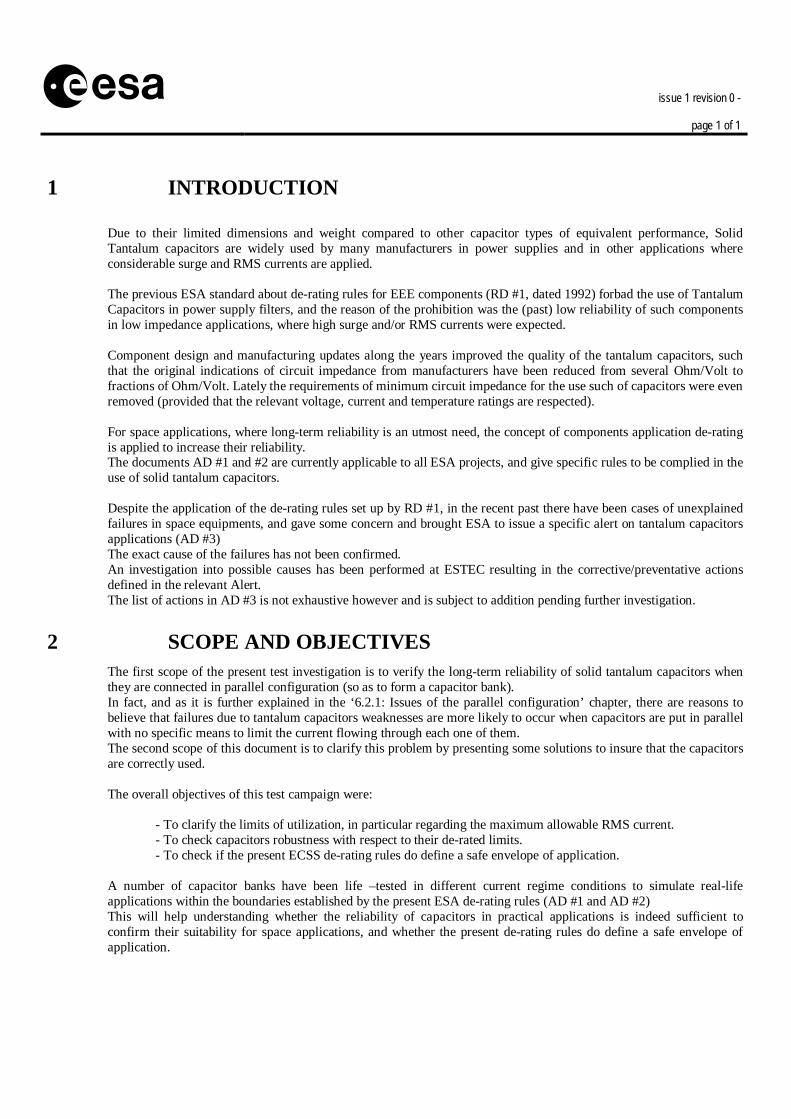
8.1 Leakage current The measurements of the 50 capacitors TAJs 22F and the 50 capacitors TAJs 10µF gave the following results:
TESTS OF TANTALUM CAPACITORS Reference22uF 35V TAJD226M035RNJ-AVX-ESA
Individual Signature of the capacitors
Reference Capacitor Bank Temperature Leakage Current Test TimeC1 CB13 22 7.01E-08 04:31.6C2 CB13 22.1 6.41E-08 04:32.1C3 CB13 22.3 1.05E-07 04:34.6C4 CB13 22.4 6.81E-08 04:32.2C5 CB13 22.7 2.04E-07 04:32.2C6 CB13 22.7 1.24E-07 04:32.3C7 CB13 22.6 7.51E-08 04:32.5C8 CB13 22.8 6.61E-08 04:31.7C9 CB13 23 6.01E-08 04:32.7
C10 CB13 22.9 6.41E-08 04:31.3C11 CB14 22.9 7.81E-08 04:31.1C12 CB14 22.7 9.42E-08 04:32.2C13 CB14 22.6 6.91E-08 04:32.5C14 CB14 22.9 7.01E-08 04:32.0C15 CB14 23 8.01E-08 04:32.2C16 CB14 23.2 1.06E-07 03:32.6C17 CB14 23.3 8.92E-08 04:30.8C18 CB14 23.3 1.66E-07 04:30.2C19 CB14 23.7 6.01E-08 04:31.5C20 CB14 23.4 6.71E-08 04:32.1C21 CB15 23.3 6.71E-08 04:31.2C22 CB15 23.3 6.41E-08 04:31.3C23 CB15 23.4 6.51E-08 04:32.2C24 CB15 23.5 2.06E-07 04:31.9C25 CB15 22.8 6.31E-08 04:31.1C26 CB15 23 6.01E-08 04:31.6C27 CB15 23 8.51E-08 04:30.3C28 CB15 23.2 6.51E-08 04:32.8C29 CB15 23.3 1.18E-07 04:32.1C30 CB15 23 5.61E-08 04:31.2C31 CB16 23 7.01E-08 04:31.3C32 CB16 23.1 1.00E-07 04:31.8C33 CB16 23.2 6.71E-08 04:32.2C34 CB16 23.2 7.31E-08 04:32.2C35 CB16 23.3 8.72E-08 04:31.3C36 CB16 23.5 6.71E-08 04:32.0C37 CB16 23.4 7.01E-08 04:32.0C38 CB16 23.3 7.51E-08 04:31.0C39 CB16 23.3 6.21E-08 04:32.0C40 CB16 21.3 6.21E-08 04:31.5C41 CB17 21.5 1.10E-07 04:31.8C42 CB17 21.9 9.22E-08 04:32.2C43 CB17 22 6.71E-08 04:32.3C44 CB17 22.1 1.75E-07 04:31.1C45 CB17 22.2 6.51E-08 04:32.1C46 CB17 22.6 7.31E-08 04:32.9C47 CB17 22.6 2.30E-07 04:30.9C48 CB17 22.7 7.21E-08 04:33.0C49 CB17 22.7 5.71E-08 04:31.3C50 CB17 22.7 9.02E-08 04:30.7
issue 1 revision 0 -
page 18 of 18
s TESTS OF TANTALUM CAPACITORS Reference
10uF 35V TAJD226M035RNJ-AVX-ESA
Individual Signature of the capacitors
Reference Capacitor Bank Temperature Leakage Current Test TimeB1 CB7 22 6.01E-08 04:29.2B2 CB7 22 6.21E-08 04:31.5B3 CB7 22 3.71E-08 04:31.9B4 CB7 22 2.70E-08 04:35.5B5 CB7 22 3.81E-08 04:31.4B6 CB7 22 2.70E-08 04:36.4B7 CB7 22 2.60E-08 04:31.3B8 CB7 22 2.30E-08 04:32.8B9 CB7 22 3.51E-08 04:33.1
B10 CB7 22 9.92E-08 04:30.3B11 CB8 22 2.00E-08 04:34.2B12 CB8 22 2.20E-08 04:32.2B13 CB8 22 2.60E-08 04:31.0B14 CB8 22 2.60E-08 04:33.3B15 CB8 22 2.50E-08 04:33.8B16 CB8 22 2.20E-08 04:33.5B17 CB8 22 2.80E-08 04:30.6B18 CB8 22 2.20E-08 04:31.2B19 CB8 22 6.31E-08 04:31.6B20 CB8 22 2.50E-08 04:33.1B21 CB9 22 1.40E-07 04:30.8B22 CB9 22 3.31E-08 04:32.1B23 CB9 22 5.31E-08 04:33.3B24 CB9 22 2.70E-08 04:30.9B25 CB9 22 2.40E-08 04:31.7B26 CB9 22 2.40E-08 04:31.2B27 CB9 22 2.50E-08 04:31.3B28 CB9 22 3.11E-08 04:32.1B29 CB9 22 2.70E-08 04:32.5B30 CB9 22 3.81E-08 04:30.7B31 CB10 22 3.41E-08 04:32.0B32 CB10 22 2.70E-08 04:29.6B33 CB10 22 2.80E-08 04:31.1B34 CB10 22 2.91E-08 04:30.9B35 CB10 22 7.01E-08 04:32.8B36 CB10 22 2.70E-08 04:32.2B37 CB10 22 2.40E-08 04:31.4B38 CB10 22 3.41E-08 04:30.6B39 CB10 22 6.21E-08 04:30.8B40 CB10 22 3.01E-08 04:30.7B41 CB11 22 2.30E-08 04:30.9B42 CB11 22 2.30E-08 04:32.0B43 CB11 22 2.10E-08 04:33.1B44 CB11 22 2.30E-08 04:29.8B45 CB11 22 2.00E-08 04:35.4B46 CB11 22 2.00E-08 04:31.3B47 CB11 22 2.60E-08 04:32.1B48 CB11 22 3.61E-08 04:31.8B49 CB11 22 1.80E-08 04:30.0B50 CB11 22 2.10E-08 04:33.3

issue 1 revision 0 -
page 19 of 19
s
Analysis of the results A statistical analysis was performed on the individual leakage currents.
Leakage Current Mean Sigma Min Max Datasheet Max
50 TC TAJ D 22uF 35V (surge current tested) 88.8nA 40.7nA 60nA 230nA 7.7uA 50 TC TAJ D 10uF 35 V (surge current tested) 35nA 12.88nA 20nA 140nA 3.5uA
Confidence level of the statistical variables: 95% The leakage current of the 2 series (10uF and 22uF) of capacitors is much lower than the maximum one given in the manufacturer datasheet. There is a ratio of 33 for the TAJ 22uF between the datasheet maximum leakage current and the maximum measured leakage current. This ratio is equal to 25 for the TAJ 10uF.
8.2 Initial Frequency characterization
8.2.1 TAJ 22UF 35V SURGE CURRENT TESTED (REF: TAJ D 226 M 035 RNJ SCT)
8.2.1.1 Initial individual Impedances The test method and set-up to measure the impedances is defined in the paragraph 11 of the present document. The initial individual impedance measurements of the TAJ 22uF gave the following results:
Impedance of C1-C10
0.01
0.1
1
10
100
100 1000 10000 100000 1000000 10000000 100000000
F [Hz]
|Z|
C2 C3 C1 C4 C5 C6 C7 C8 C9 C10 typical Fig 17: Impedances of 10 capacitors TAJD 22uF 35V (C1-C10)

issue 1 revision 0 -
page 20 of 20
s The plots of the impedances of the capacitors C11 to C50 are available in annex 1. Analysis of the results: As shown by the figures 7 and in annex 1 of the impedance in function of the frequency, the individual impedances do not present significant differences between each other. It was as expected, since the capacitors come from the same lot. However a non-negligible difference remains between the measurements results and the typical impedance given by the manufacturer. It is important to highlight that in the impedances characterization, the accuracy and the stability of the frequency analyzer is checked by the measure of a stable PM90 capacitor before and after the tantalum capacitor impedances measurements.
8.2.1.2 ESR=f(F) and Capacitance X=f(F) With the measurement of the impedance (module and phase), it is possible to plot the ESR and the capacitance in function of the frequency of the capacitors. The impedance can be decomposed in two parts:
ω).(1)()(FXj
FESRFZ⋅
+=−
Where, F is the frequency [Hz], X the capacitance of the capacitor [F], and ω the pulsation [rad/s]. The next paragraph presents the frequency –dependent capacitance and ESR of the capacitors C1-C10, as well as a statistical analysis.

issue 1 revision 0 -
page 21 of 21
s
+
ESR=f(F) C1-C10
0.01
0.1
1
10
100 1000 10000 100000 1000000 10000000 100000000F [Hz]
ESR
[Ohm
s]
ESR-C1 Typical ESR-C2 ESR-C3 ESR-C4 ESR-C5 ESR-C6 ESR-C7 ESR-C8 ESR-C9 ESR-C10
X=f(F) C1-C10
-3.6E-05
-2.6E-05
-1.6E-05
-6.0E-06
4.0E-06
1.4E-05
2.4E-05
3.4E-05
100 1000 10000 100000 1000000 10000000F [Hz]
X [F
]
Typical X-C1 X-C2 X-C3 X-C4 X-C5 X-C6 X-C7 X-C8 X-C9 X-C10
FIG 18A AND 13B: ESR (F) AND CAPACITANCE X(F) OF 10 CAPACITORS TAJD 22UF 35V (C1-C10)

issue 1 revision 0 -
page 22 of 22
s
Analysis of the results: In the datasheet the ESR is measured at 100KHz and the capacitance at 120Hz. The table below summarises the ESRs and capacitances of the capacitors TAJ D 22uF 35V at these frequencies and at ambient temperature.
X ESR X ESR Capacitance ESRCapacitor at 120Hz at 100KHz Capacitor at 120Hz at 100KHz
[uF] [Ohms] [uF] [Ohms] Mean 21.29 Mean 0.20144C1 21.49 0.197 C26 21.23 0.202 Standard Error 0.074377 Standard Error 0.0006235C2 21.02 0.204 C27 20.23 0.199 Median 21.41 Median 0.2015C3 20.33 0.201 C28 21.03 0.206 Mode 21.32 Mode 0.204C4 21.09 0.198 C29 21.69 0.210 Standard Deviation 0.525924 Standard Deviation 0.0044085C5 20.11 0.204 C30 21.43 0.199 Sample Variance 0.276596 Sample Variance 1.944E-05C6 20.22 0.199 C31 21.32 0.209 Kurtosis -0.357143 Kurtosis 0.7139474C7 21.32 0.206 C32 21.66 0.205 Skewness -0.79803 Skewness -0.637983C8 21.64 0.203 C33 21.96 0.201 Range 1.9 Range 0.021C9 21.85 0.207 C34 21.53 0.196 Minimum 20.11 Minimum 0.189C10 21.20 0.200 C35 20.52 0.196 Maximum 22.01 Maximum 0.21C11 21.03 0.207 C36 21.71 0.198 Sum 1064.5 Sum 10.072C12 20.56 0.200 C37 21.39 0.199 Count 50 Count 50C13 21.79 0.200 C38 21.80 0.203 Largest(1) 22.01 Largest(1) 0.21C14 21.12 0.201 C39 20.35 0.200 Smallest(1) 20.11 Smallest(1) 0.189C15 21.75 0.207 C40 20.82 0.205 Confidence Level(95.0%) 0.149466 Confidence Level(95.0%) 0.0012529C16 21.52 0.204 C41 21.79 0.201C17 21.53 0.202 C42 21.58 0.206C18 21.89 0.204 C43 21.09 0.199C19 21.30 0.193 C44 21.75 0.204C20 21.78 0.205 C45 21.78 0.205C21 21.31 0.190 C46 22.01 0.204C22 20.32 0.202 C47 21.08 0.189C23 21.76 0.200 C48 20.60 0.196C24 21.49 0.206 C49 21.46 0.199C25 21.32 0.198 C50 21.95 0.203
0
1
2
3
4
5
6
19 19.5 20 20.5 21 21.5 22 22.5 23Cs [uF]
Nb
of s
ampl
e
0
0.1
0.2
0.3
0.4
0.5
0.6
0.7
0.8
P(x)
TAJD226K035RNJ-AVX-ESATEC-ECPCapacitance
0
1
2
3
4
5
6
7
180 185 190 195 200 205 210 215 220ESR [m ohms]
Nb
of s
ampl
e
0
0.01
0.02
0.03
0.04
0.05
0.06
0.07
0.08
0.09
0.1
P(x)
TAJD226K035RNJ-AVX-ESATEC-ECPESR
Fig 19: Capacitances and ESRs statistical analysis of the 50 capacitors (C1-C50) TAJD 22uF 35V

issue 1 revision 0 -
page 23 of 23
s The initial tolerance of the capacitors is +/-20%. All the capacitance values are in this range. The low number of measurements (50) explains the fact that the repartition of the capacitances measured is not represented by a Gaussian and also why the histogram is not centered exactly on the value 22uF. The typical value of the ESR of the TAJ D 22uF 35V at 100KHz and 25degC is 138.7mΩ (from the datasheet software SpitanII, available on the web-site of AVX). This typical value is much lower than the measured values. The typical ESR performances of the given in the datasheet are better than the ESRs performances of the measured capacitors. The mean of the overall ESRs measurements is 201mΩ and the values are comprised in the range +/-6% of the mean. This narrow range of values is probably due to the fact that the capacitors come from the same lot. The maximum ESR is specified at 900m Ω in the manufacturer datasheet (at100Khz). The measured values are much lower than this value. The manufacturer takes margin probably for eventual differences of ESR among different lots.
8.2.2 TAJ 10UF 35V SURGE CURRENT TESTED (REF: TAJ D 106 K 035 RHJ SCT)
8.2.2.1 Initial individual Impedances The initial single impedances of the TAJ10uF give the following results:
Impedance of B1-B10
0.01
0.1
1
10
100
1000
100 1000 10000 100000 1000000 10000000 100000000
F [Hz]
|Z|
B2 B3 B1 B4 B5 B6 B7 B8 B9 B10 Typical Fig 20: Impedances of 10 capacitors (B1-B10) TAJD10uF 35V

issue 1 revision 0 -
page 24 of 24
s Analysis of the results: As for the capacitors TAJ D 22uF, the TAJ D 10uF present impedances very close between them (same lot), but different in comparison with the typical one given by the manufacturer. From these measurements, the ESRs and the capacitances of the capacitors were plotted.
8.2.2.2 ESR=f(F) and Capacitance X=f(F) With the measurement of the impedance (module and phase), it is possible to plot the ESR and the capacitance in function of the frequency of the capacitors. The impedance can be decomposed in two parts:
ω).(1.)()(FX
jFESRFZ +=−
where F is the frequency [Hz], X the capacitance of the capacitor [F], and ω the pulsation [rad/s]. The next paragraph presents for the capacitors B1-B10, their capacitances and ESRs in function of the frequency as well as a statistical analysis.
ESR=f(F) of B1-B10
0.01
0.1
1
10
100 1000 10000 100000 1000000 10000000 100000000
F [Hz]
ESR
B2 B3 B1 B4 B5 B6 B7 B8 B9 B10 Typical

issue 1 revision 0 -
page 25 of 25
s X=f(F) of B1-B10
-1.50E-05
-5.00E-06
5.00E-06
1.50E-05
100 1000 10000 100000 1000000 10000000 100000000
F [Hz]
X
B2 B3 B1 B4 B5 B6 B7 B8 B9 B10 Typical Fig 21a and b: ESRs and Capacitances of 10 capacitors (B1-B10) TAJD 10uF 35V

issue 1 revision 0 -
page 26 of 26
s The plots of ESRs=f(F) and X=f(F) of the capacitor B11 to B50 are available in annex 2. Analysis of the results: In the datasheet the ESR is measured at 100KHz and the capacitance at 120Hz. The table below summarises the ESRs and capacitances of the capacitors TAJ D 10uF 35V at these frequencies and at ambient temperature and pressure.
X ESR X ESR Capacitance ESRCapacitor at 120Hz at 100KHz Capacitor at 120Hz at 100KHz
[uF] [mOhms] [uF] [mOhms] Mean 10.21 Mean 305.76315B1 10.23 309.912 B26 10.26 306.023 Standard Error 0.01238 Standard Error 1.253705B2 10.14 307.268 B27 10.18 305.587 Median 10.23281 Median 306.25648B3 10.09 296.907 B28 10.17 313.004 Mode #N/A Mode #N/AB4 10.08 297.648 B29 10.27 300.191 Standard Deviation 0.08754 Standard Deviation 8.8650331B5 10.14 304.038 B30 10.25 311.162 Sample Variance 0.007663 Sample Variance 78.588812B6 10.32 295.581 B31 10.20 318.453 Kurtosis -1.18029 Kurtosis 1.8502115B7 10.26 289.325 B32 10.33 315.335 Skewness -0.137861 Skewness -0.449533B8 10.08 296.101 B33 10.27 309.710 Range 0.285684 Range 52.925186B9 10.17 296.644 B34 10.09 329.226 Minimum 10.07104 Minimum 276.30094B10 10.11 276.301 B35 10.09 312.620 Maximum 10.35673 Maximum 329.22612B11 10.26 304.748 B36 10.08 311.869 Sum 510.5002 Sum 15288.157B12 10.36 306.279 B37 10.23 301.210 Count 50 Count 50B13 10.24 308.302 B38 10.22 312.473 Largest(1) 10.35673 Largest(1) 329.22612B14 10.26 301.567 B39 10.35 297.891 Smallest(1) 10.07104 Smallest(1) 276.30094B15 10.35 302.760 B40 10.25 299.030 Confidence Level(95.0%) 0.024879 Confidence Level(95.0%) 2.519413B16 10.31 310.237 B41 10.31 309.117B17 10.25 314.755 B42 10.10 314.216B18 10.08 312.380 B43 10.32 304.063B19 10.26 312.180 B44 10.14 308.771B20 10.21 303.233 B45 10.24 298.845B21 10.23 298.789 B46 10.07 309.740B22 10.30 309.772 B47 10.18 291.961B23 10.32 308.230 B48 10.08 321.120B24 10.31 303.926 B49 10.17 316.443B25 10.11 296.977 B50 10.19 306.234
0
1
2
3
4
5
6
10 10.05 10.1 10.15 10.2 10.25 10.3 10.35 10.4X [uF]
Nb o
f sam
ple
0
0.5
1
1.5
2
2.5
3
3.5
4
4.5
5
P(x)
TAJD106K035RHJ-AVX-ESATEC-ECPX
0
0.5
1
1.5
2
2.5
3
3.5
4
4.5
270 278 285 293 300 308 315 323 330ESR [m ohms]
Nb o
f sam
ple
0
0.005
0.01
0.015
0.02
0.025
0.03
0.035
0.04
0.045
0.05
P(x)
TAJD106K035RHJ-AVX-ESATEC-ECPESR
Fig 22: Capacitances and Esrs statistical analysis of the 50 capacitors (B1-B50) TAJD 10uF 35V

issue 1 revision 0 -
page 27 of 27
s The initial tolerance of the capacitors is +/-10%. All the capacitances measured do belong to this range. As for the 22uF capacitors, the low number of measurements (50) explains the fact that the repartitions of the capacitances and ESRs measurements are not represented by a Gaussian and also why the histograms are not centered on the typical value. The typical value of the ESR of the TAJ D 10uF 35V at 100KHz and 25degC is 168.3mΩ (from the datasheet software SpitanII, available on the web-site of AVX). This value is much lower than the measured values. The frequency impedance performances of the typical impedance given in the datasheet are better than the performances of the measured capacitors. The mean of the overall ESRs measurements is 305.8mΩ and the values are comprised in the range +/-10% around this mean. This narrow range of values is probably due to the fact that the capacitors come from the same lot. The maximum ESR is specified at 1Ω (100 KHz) in the manufacturer datasheet. The measured values are much lower than this value. The manufacturer takes a margin probably for eventual differences of ESR among different lots.
9 CAPACITOR SOLDERING A total of 10 capacitor banks were soldered. Each capacitor bank consists of 10 capacitors in parallel (same type and value).
Capacitors ref. Type Caps. Labels CB Labels B1 to B10 CB7 B11 to B20 CB8 B21 to B30 CB9 B31 to B40 CB10
TAJD106K035RHJ
TAJD 10uF 35V ESA SCT
B41 to B50 CB11
Capacitors ref. Type Caps. Labels CB Labels C1 to C10 CB13
C11 to C20 CB14 C21 to C30 CB15 C31 to C40 CB16
TAJD226M035RNJ
TAJD 22uF 35V ESA SCT
C41 to C50 CB17
9.1 Soldering conditions
9.1.1 AVX GUIDELINES The guidelines of the manufacturer AVX for IR reflow are the following: ⋅ The slope of the component land temperature profile has to be lower than 2degC/sec. ⋅ The peak of temperature has to be lower than 220degC (see figure 23). ⋅ The period of time when the component land temperature is higher than the solder melting temperature
(186degC) has to be shorter than 45 seconds.

issue 1 revision 0 -
page 28 of 28
s
Fig 23. Allowable range of peak temp. /time combination for IR reflow
AVX summarizes these three precautions with the following graph (Fig. 24).
Fig. 24: Ideal temperature profile for IR reflow.

issue 1 revision 0 -
page 29 of 29
s
9.1.2 ESA ALERT After failures of TC, ESA emitted recommendations concerning the soldering process in the ESA-Alert. The extract of this alert is the following:
In other words, the maximum peak of component land temperature has to be lower than 210degC. The slopes and the period time when the temperature is higher than 186degC remain the same.
9.1.3 TEMPERATURE PROFILES OF THE TESTED CAPACITOR BANKS The capacitors were soldered by NETRONIC (Bogardeind 164, 5664 EN Geldrop,The Netherlands). This company works sometimes for ESTEC (sections SCI-AP and SCI-AI). With the help of Bengt Johlander and Johannes Heida from these two sections, it was decided to ask Netronic to solder the capacitors. During the soldering process it appeared that it is difficult to follow the temperature profile (Fig. 24) of AVX. Another capacitor bank (CB12) with commercial capacitors (22uF, not surge current tested) was used to measure the component land temperature. Fig. 25 presents the measured profile. This temperature profile shows that the capacitors were soldered safely within the applicable limits. The peak of temperature is 200degC, the increased slope is lower than 2deg/sec and the period when the temperature is higher than 186 (solder melting point) is close to 45 seconds.
Fig. 25: Soldering conditions (guidelines, recommendations and measurements)
Carole Villette, and Gianni Corocher from the Materials Mechanics and Processes Section (TEC-QMM) have inspected the capacitors after the soldering process according to ESA PSS 738. Due to the temperature profile (low peak temperature) many solder joints show discontinuities, voids and/or porosity, which will not be acceptable for flight equipment according to the standard. This might have a consequence on the electrical connections between the capacitors and the PCB if they are mechanically stressed and/or with thermal

issue 1 revision 0 -
page 30 of 30
s cycles. However for this study, it was decided that the capacitor banks were fit for the relevant tests (no thermal or mechanical stress was foreseen), and in fact the capacitors stayed well connected to the PCBs until the end of the test campaign.
Fig. 26a and b: Capacitor bank after soldering process and printed circuit of the PCB

issue 1 revision 0 -
page 31 of 31
s
9.2 Check of the capacitor bank signatures after the soldering process
Each capacitor was characterized individually before the soldering process (part 8). To be sure that the soldering process didn’t affect the signatures of the capacitors, the capacitor banks were characterized after the soldering process.
9.2.1 LEAKAGE CURRENTS AFTER THE SOLDERING Leakage current results: Capacitor banks (CB13 to CB17) of TAJD 22uF 35V (C1 to C50)
Sum of single Caps CBLeakage Current CB Leakage Current Ratio
C1-C10 CB13 9.02E-07 9.27E-07 1.03C11-C20 CB14 8.81E-07 9.37E-07 1.06C21-C30 CB15 8.50E-07 8.59E-07 1.01C31-C40 CB16 7.34E-07 7.41E-07 1.01C41-C50 CB17 1.03E-06 1.07E-06 1.04
Capacitor banks (CB7 to CB11) of TAJD 10uF 35V (B1 toB50)
Sum of single Caps CBLeakage Current CB Leakage Current Ratio
C1-C10 CB7 4.34765E-07 4.09756E-07 0.94247679C11-C20 CB8 2.79492E-07 2.92683E-07 1.047196433C21-C30 CB9 4.22744E-07 5.07317E-07 1.200057334C31-C40 CB10 3.65644E-07 3.80488E-07 1.040597661C41-C50 CB11 2.31407E-07 2.43902E-07 1.05399641
Leakage current analysis: Except for the capacitor bank CB9, the leakage current before and after the soldering process is the same. However the leakage current of the capacitor bank CB9 is much lower than the maximum given by the datasheet (35uA for the 10 capacitors in parallel). The soldering process did not affect the leakage current of the capacitors.
9.2.2 FREQUENCY CHARACTERIZATIONS AFTER THE SOLDERING Capacitor bank CB13 of TAJD 22uF 35V (C1 to C50) To see if the soldering process has an effect on the impedances before and after the soldering process, the capacitor banks were characterized and compared to the calculated total impedance with the 10 individual capacitors impedances measured before the soldering process. The measurements and calculations gave the following results.

issue 1 revision 0 -
page 32 of 32
s Impedance of CB13 (Reference CB)
0.01
0.1
1
10
100
100 1000 10000 100000 1000000 10000000 100000000
F [Hz]
|Z|
CB13 after soldering process C1//C2//C3//C4//C5//C6//C7//C8//C9//C10 Fig. 27: Comparisons of the impedances of CB13 before and after the soldering process for the TAJD 22uF 35V
Capacitor banks CB7 of TAJD 10uF 35V (B1 to B50)
Impedance of CB7
0.01
0.1
1
10
100
100 1000 10000 100000 1000000 10000000 100000000
F [Hz]
IZI
Cii// CB7 after soldering process
Fig. 28: Comparisons of the impedances of CB7 before and after the soldering process for the TAJD 10uF 35V (B1...B10)
The graphs of the comparison of the capacitor banks CB7 to CB11 and CB14 to CB17 are available in annex 7.

issue 1 revision 0 -
page 33 of 33
s Analysis of the frequency measurements: The capacitances (at low frequency) of all the capacitor banks are exactly equal to the sum of the individual capacitances of the single capacitors before the soldering process. In high frequency the slopes of the impedances have changed a little bit. In other words the series inductance has increased. Moreover the amplitude of the impedance at the frequency resonance is higher due to the parasitic resistors added. The consequence of these parasitic elements introduction (resistor and inductor) is also visible: the frequency resonance of the capacitor bank is lower than the resonance of the expected resonance with the calculated impedance of the individual measured impedances in parallel.
10 POWER TESTS CONDITIONS
10.1 General conditions The tests performed concern only the TAJD 22uF 35V (CB13 to CB17).
All tests were performed in ambient pressure conditions. The life test of the capacitor banks were performed at a controlled temperature (85°C ± 3°C) by placing
(gluing) the relevant PCB containing the 10 capacitors in parallel on the temperature-controlled plates described in this chapter.
The frequency of operation of the converter to generate the RMS current through the capacitor bank was 131 KHz ± 5%.
The capacitor banks were stressed at the de-rated voltage. Each capacitor bank was tested for overall leakage current and impedance at the beginning of the test
campaign (after the soldering process) and at approximately fixed intervals during the life testing (every 100 hours). The detailed test set up and test conditions are specified in paragraph 11.
10.2 Capacitor banks conditions
10.2.1 CB 13: REFERENCE CB 13 is the reference capacitor bank. This capacitor bank was not tested, but its signature was measured when the other capacitor banks were characterized at approximately fixed intervals during the life testing (every 100 hours).
10.2.2 CB 14: CONTINUOUS REGIME 1 CB 14 is the capacitor bank subjected to continuous RMS current regime 1, and within the applicable current de-rating conditions defined in AD #1, AD #2 and at the end of this chapter (“10.3 definition of rms current in regime 1”).
10.2.3 CB 15: CONTINUOUS REGIME AT 2.5ARMS The Worst Case methods described in paragraph II take into account all the possible variations between capacitors using the manufacturer data. At 2.1 - 2.2 A rms, the user is sure that the de-rated power dissipation limit will not be reached (75mW). To validate the safe utilization domain (rms current between 0 and 2.1-2.2A rms found with the worst-case analyses) CB15 was subjected to continuous RMS current at approximately 2.5A rms.

issue 1 revision 0 -
page 34 of 34
s 10.2.4 CB 16: INTERMITTENT REGIME AT 2.5ARMS The specific test condition for CB 16 is representative of an application with frequent start-stop cycles (for example output capacitor banks of power supplies connected to digital equipments). The Worst Case methods described in paragraph II take into account all the possible variations among capacitors using the manufacturer data. At 2.1 - 2.2 A rms, the user is sure that the de-rated power dissipation limit will not be reached (75mW). To validate the safe utilisation domain (rms current between 0 and 2.1-2.2A rms found with the worst-case analyses), CB16 was subjected to intermittent RMS current from 0% to 100% of 2.5 A rms with period of stress of 5 minutes.(the capacitor bank was electrically stressed only for half of the period i.e. for 2minutes and 30 seconds).
10.2.5 CB 17: INCREASED REGIME Due to the unknown operating rms current corresponding to the de-rated power dissipation limit, the capacitor bank CB17 was tested at different stress regimes. CB17 was initially stressed below its de-rated power dissipation limit starting at 2.5 A RMS and progressively the current was increased in steps (of 1 RMS A) after each periodical signature testing (every 100 hours).
10.3 Regime 1 conditions Two analyses were performed to find the maximum allowable RMS current corresponding to the de-rated power dissipation criteria (75mW) for the particular capacitor bank CB14, taking into account of the individual capacitor impedances measured before the soldering process.
10.3.1 FIRST ANALYSIS: RLC EQUIVALENT CIRCUIT From the measurements of the capacitors impedances, the capacitors RLC equivalent circuits were identified. A simulation was performed with the identified RLC circuits. Fig .28 and 29 depict respectively the circuit used for this simulation and the simulation results.
Fig. 29: Simulation with the CB14 (C11 to C20) in transient with the equivalent RCL circuit measured before the
soldering process.

issue 1 revision 0 -
page 35 of 35
s
Fig.30a and b: simulation with the RLC equivalent circuits of the capacitors of CB14, identified before the soldering process.
Taking into account of the set-up used to produce the current across the capacitor bank, also a more realistic current waveform (trapezoidal, see Figure 30) was simulated to check the relevant impact on the individual power dissipation
Capacitor bank CB14 current
Individual RMS Power Dissipations
Fig.31a and b: simulation with the RLC equivalent circuits of the capacitors of CB14, identified before the soldering
process.
In both cases the limit of the de-rated power dissipation of CB14 was reached at least in one of the capacitors with a total maximum RMS current of 6.5A RMS.
10.3.2 SECOND ANALYSIS: CURRENT VECTORS SUM From the measurements of the capacitors impedances of CB14 before soldering, the method of the current vectors sum was applied to find the limit in rms current corresponding to the de-rated power dissipation: By assuming that the individual capacitor currents have the same type of waveforms (square wave, with a duty cycle of 50%), but with different amplitudes, it is possible to calculate, the amount of RMS current that can be injected in each single capacitor to respect the de-rated power dissipation (75mW) criteria with the measured ESR of each single capacitor. For instance, for the capacitor C11 of CB14, the following table gives the results:

issue 1 revision 0 -
page 36 of 36
s
Fig.32a: Details of the power dissipation calculation in one capacitor
The amplitude of the square wave current in this capacitor is 0.64A to reach the de-rated power dissipation (75mW). At each harmonic frequency, the rms values of the harmonic current in the capacitor C11 were identified. These values give the modules of the capacitor C11 current vectors at each harmonic frequency. Note, that the phases of the capacitor C11 current vectors are linked to their impedances. Then the RMS current of the capacitor bank is calculated by summing the individual rms current vectors at each harmonic frequency. Square root of the sum square of the harmonic sums gives the overall RMS current than can be injected in the capacitor bank. For the capacitor bank 14, it gave the following table:
Fig.32b: Details of the power dissipation calculation in the capacitor bank CB14 with the vectors sum method

issue 1 revision 0 -
page 37 of 37
s For this capacitor bank, with this second approach, the total CB14 rms current was evaluated at 6ARMS to fulfill the de-rated power dissipation criteria in each single capacitor. The advantage of this method was to use the real measured ESRs and not an approximate equivalent circuit. This method also presents a drawback concerning the waveforms of the current in the single capacitor: they are always assumed to be square wave with a duty cycle of 50%. This assumption is not rigorous. Besides, the impedances of the capacitors may change during the life testing and consequently the ESRs too.
10.3.3 CONCLUSION: DEFINITION OF THE REGIME 1 RMS CURRENT In the regime one, the level of the rms capacitor bank current was evaluated to reach the de-rating power dissipation limit. Two calculations were performed. The first one was using the individual ESR=f(F) of each capacitor, and the second one, by using the RLC model of each individual capacitor, identified for both before the soldering process. For CB14, the de-rated power dissipation limits correspond to a maximum capacitor bank current in the area of 6 - 6.5 A RMS. To be sure that this capacitor bank was stressed at the operating point of the de-rated power dissipation, the CB14 was stressed at 7A rms.

issue 1 revision 0 -
page 38 of 38
s
11 INSTRUMENTS AND MEASUREMENT METHODS
11.1 Impedances measurement The impedances were measured with an Impedance Gain-Phase analyser HP4194A from 100Hz to 40MHz at ambient T° and pressure (Fig. 33). The perturbation injected in the capacitors was 0.5V RMS with a DC bias of 2.2 volts.
Fig. 33: Frequency Analyser
Before and after each characterization, the test set up was validated by the characterization of a “stable” PM90SR 10uF, esr of 10mΩ at ambient temperature). This simple test allows checking the stability of the frequency analyser and the quality of the measurements. Fig. 34 shows how the equipment gives a good appreciation of this stable capacitor.
Impedance of a PM90SR
0.01
0.1
1
10
100
1000
100 1000 10000 100000 1000000 10000000 100000000
F [Hz]
Z
PM90SR -1.txt PM90SR -2.txt PM90SR after.txt test PM90SR - 3.txt test PM90SR - 4 test PM90SR - 5.txt test PM90SR -6.txt
Fig. 34: Verification of the measurements with a stable capacitor PM90SR

issue 1 revision 0 -
page 39 of 39
s The impedance characterizations of the PM90 SR were always very close each other. The equivalent circuit RLC in series of the PM90SR was also identified.
Example of RLC equivalent circuit of a PM90SR 10uF given by the frequency analyser: R=10.0964mΩ, L=13.7734nH, C=9.99071uF.
11.2 Leakage currents measurement The leakage current depends on three factors: time, temperature and voltage applied to the capacitors. For more detail concerning the leakage current of tantalum capacitors, please refer to RD#2. The measurements of the leakage current were realised after 4minutes and 30 seconds, at ambient temperature and pressure, and with a dc voltage of 35V (+/-2%). A resistor is placed in series with the capacitor to limit the charging current and to read the leakage current via the voltage drop of this resistor. For the single capacitors, a resistor of 100kΩ is placed in series with the TC. The leakage current is very small and 100kΩ are needed to perform a sufficiently accurate measurement of the current. The leakage current of the single TC was measured with the same principle of clip connector than for the impedances with frequency analyser. Assuming that the capacitance of the CB is about 10 times the capacitance of one single TC (10 caps are in parallel on one CB), a resistor of 10kΩ is placed in series with the CB for the CB leakage current measurements to conserve the same time constant of charge of the tantalum capacitor bank than during the measure of the leakage current of the single tantalum capacitor. This series resistor allows limiting the charge and to have a good accuracy of the current reading. A steady source of power, such as a regulated power supply is used. Fig 35 presents the schematic of the circuit used to measure the leakage current.
Fig. 35: Circuit for the leakage measurement
The voltage source used to supply the capacitor was 2 power supplies in series (Delta Elektronika ES-030-5 (30V-5A)). During the measurement, a Philips multimeter PM2525 with a thermocouple was used to measure the ambient temperature. Two multimeters measured the voltage of the power supply (Philips PM2525) and the leakage current via the voltage drop of the series resistor (Fluke 45 Dual Display Multimeter).
11.3 Temperature Measurement The thermal camera of the TEC-QCT has been used to take picture of the temperature capacitors (Flir Thermacamera SC3000). This device is exceptionally used in the TEC-EP laboratory (Fig. 36).

issue 1 revision 0 -
page 40 of 40
s
Fig. 36: Thermal Camera
A thermal picture of a capacitor bank painted in black was taken to find the best place to measure the temperature with thermocouples during the tests (Fluke 54II and Keithley 871). Fig. 37 reports the picture taken.
Fig. 37: Thermal Pictures of the TC on CB

issue 1 revision 0 -
page 41 of 41
s The warmest areas are located between the capacitors. It is important to note that the distances between each capacitor respect the recommended emplacements given by the manufacturer.. After the measurement it was decided to use thermocouples and to place them between two capacitors to measure their body temperature.
12 FACILITIES FOR THE POWER TESTS
12.1 Temperature controlled plates Temperature controlled plate were developed to guarantee a capacitors temperature of 85degC. The capacitor banks have been glued on one face of the aluminium plate. On the other side, 12 resistors of 1Ω are connected in series and can dissipate several ten of watts. The drawings of the plates are shown on annex 8.
Fig.38: Resistors face of the aluminum plate The temperature of the plate is controlled via a control card, detailed in annex 8.
12.2 Converters for electrical stress The topology of the converters used to stress electrically the capacitor banks is a step-down converter (single inductor buck topology). Fig. 39 illustrates the topology with the theoretical waveforms of current at different points of the circuit.

issue 1 revision 0 -
page 42 of 42
s
I
tAC absorption
I
t
DC currentI
t
Pulsed Current
I
tAC absorption
I
t
DC currentI
t
Pulsed Current
Fig. 39: buck converter to stress electrically the capacitor bank
The current injected in the capacitor bank is almost square wave. The slopes when the current is positive are due to the presence of the inductors. The capacitor bank and the inductor L1 form an input filter, which allows the power supply to deliver a constant current. The capacitor bank absorbs the AC part of the MFET M3 current. The elements in the square area are optional and only used for the capacitor bank CB16, stressed by intermittent current application. Fig. 43 illustrates the typical waveform of current injected in the capacitor bank.
Fig. 40: Example of current injected in the capacitor banks

issue 1 revision 0 -
page 43 of 43
s 12.3 Test set-ups
12.3.1 SET-UP FOR THE IMPEDANCES CHARACTERIZATION Fig. 38a and b present the set-up used to identify the signatures of the capacitors.
Fig. 41a and b: Frequency Analyser and its clip connector
For the single characterization a clip connector was used to avoid hand soldering (which might affect the capacitor electrical performances).
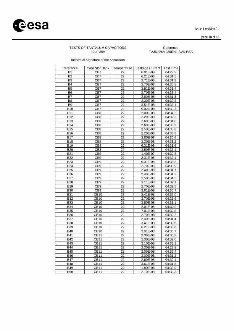
12.3.2 SET-UPS FOR THE POWER TESTS Figures 45, 46, 47 show the complete stress set-up for the capacitor banks. The PCBs are mounted on the heating plates, close to the power converters.
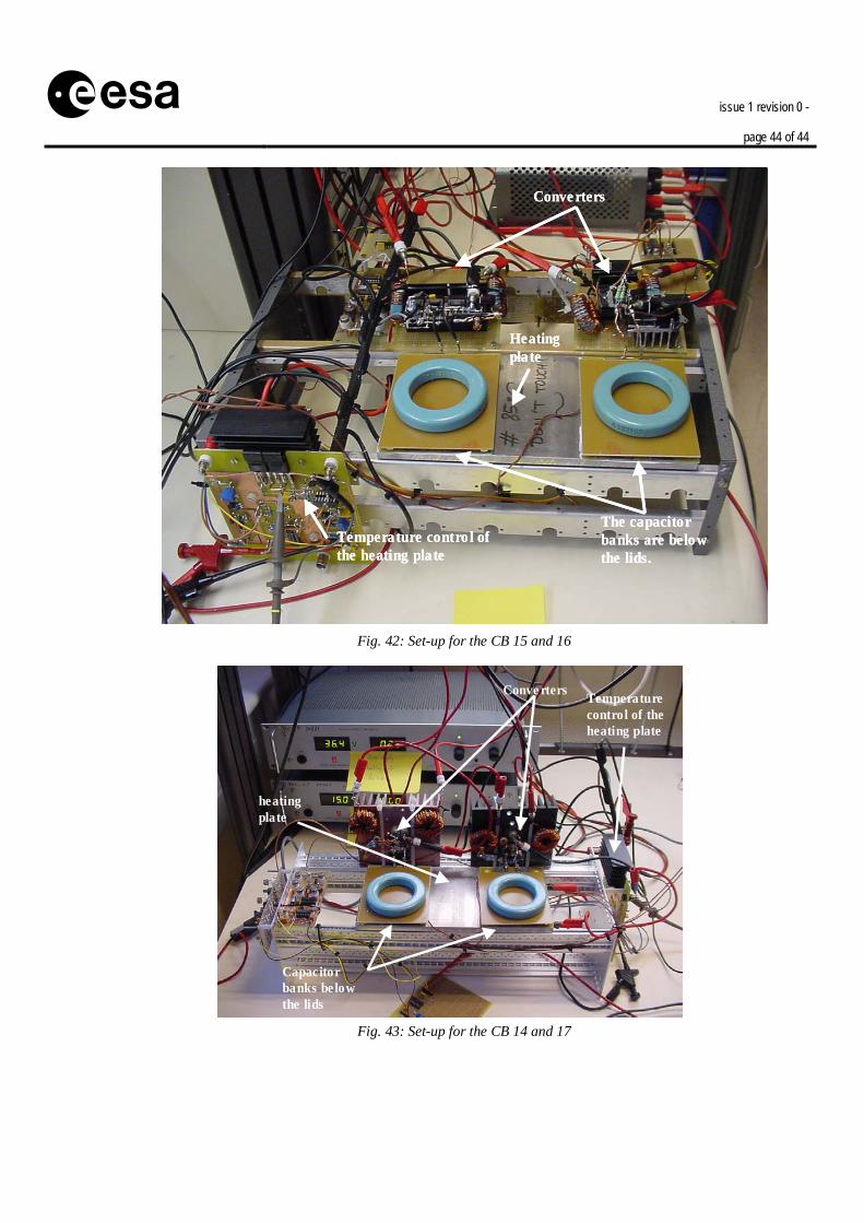
issue 1 revision 0 -
page 44 of 44
s
Conve rters
Heating plate
Temperature control of the heating plate
The capacitor banks are below the lids.
Conve rters
Heating plate
Temperature control of the heating plate
The capacitor banks are below the lids.
Fig. 42: Set-up for the CB 15 and 16
Conve rters Temperature control of the heating plate
Capacitor banks below the lids
heating plate
Conve rters Temperature control of the heating plate
Capacitor banks below the lids
heating plate
Fig. 43: Set-up for the CB 14 and 17

issue 1 revision 0 -
page 45 of 45
s
Conve rters
Temperature control of the heating plate
Capacitor banks
Conve rters
Temperature control of the heating plate
Capacitor banks
Fig. 44: Set-up for the CB 15 and 16

issue 1 revision 0 -
page 46 of 46
s
13 CAPACITOR BANKS LIFE TESTS During the test period, no failure occurred. All the capacitor banks were tested for about 1000 hours.
13.1 Evolution of the Capacitor banks leakage current during the life tests
Fig. 45: Leakage Current during the life testing
Capacitor Bank CB13 (reference, not stressed) Capacitor Bank CB14 (continuous regime, 7 RMSA) Capacitor Bank CB15 (continuous regime, 2.5 RMSA) Capacitor Bank CB16 (intermittent regime, 2.5 RMS A) Capacitor Bank CB17 (increase regime from regime, 2.5 RMS A to 10 RMS A) Analysis of the results The leakage currents were always lower than the maximum expected (sum of individual max). Nevertheless the leakage current of CB14 – subject to the highest RMS current at the beginning of the test campaign- shows rather large variations.

issue 1 revision 0 -
page 47 of 47
s
13.2 Evolution of the Capacitor banks impedances during the life tests
13.2.1 CAPACITOR BANK CB13 (REFERENCE, NOT STRESSED)
0.01
0.1
1
10
100
100 1000 10000 100000 1000000 10000000 100000000
F [Hz]
|Z|
CB13-1 CB13-2 CB13-3 CB13-4 CB13-5 CB13-6 CB13-7 CB13-8 CB13-9 CB13-10 CB13-11 CB13-12 Fig. 46: Impedance of CB13 during the life testing of CB14-CB15-CB16-CB17
CB13 was characterized: Name After the soldering process. CB13-1 When CB14&CB17 were characterized after 30 hours of test, And CB15&CB16 after 68 hours of test.
CB13-2
When CB14&CB17 were characterized after 102 hours of test, And CB15&CB16 after 141 hours of test.
CB13-3
When CB14&CB17 were characterized after 204 hours of test, And CB15&CB16 after 244 hours of test.
CB13-4
When CB14&CB17 were characterized after 296 hours of test, And CB15&CB16 after 335 hours of test.
CB13-5
When CB14&CB17 were characterized after 401 hours of test, And CB15&CB16 after 440 hours of test.
CB13-6
When CB14 was characterized after 480 hours of test. CB13-7 When CB14&CB17 were characterized after 506 hours of test, CB15&CB16 after 546 hours of test.
CB13-8
When CB14 was characterized after 540 hours of test. CB13-9 When CB14&CB17 were characterized after 610 hours of test, CB15&CB16 after 667 hours of test.
CB13-10
When CB14 was characterized after 655 hours of test. CB13-11 When CB14&CB17 were characterized after 718 hours of test, CB15&CB16 after 776 hours of test.
CB13-12
When CB14&CB17 were characterized after 816 hours of test, CB15&CB16 after 774 hours of test.
CB13-13
When CB14&CB17 were characterized after 893 hours of test CB13-14 When CB14&CB17 were characterized after 972 hours of test, CB15&CB16 after 1027 hours of test.
CB13-15
Analysis of the results: The impedance of the reference capacitor bank (CB13) remains the same during all the tests.

issue 1 revision 0 -
page 48 of 48
s
13.2.2 CAPACITOR BANK CB14 (CONTINUOUS REGIME 7 A RMS)
Impedance of CB14
0.01
0.1
1
10
100
100 1000 10000 100000 1000000 10000000 100000000F [Hz]
|Z|
CB14-1 CB14-2 CB14-3 CB14-4 CB14-5 CB14-6 CB14-7 CB14-8 CB14-9 CB14-10CB14-11 CB14-12 CB14-13 CB14-14 CB14-15 CB14-16 CB14-17 CB14-18
Fig. 47: Impedance during the life testing of CB14
CB14 was characterized: Name After the soldering process. CB14-1 After 30 hours of test. CB14-2 After 102 hours of test. CB14-3 After 204 hours of test. CB14-4 After 296 hours of test. CB14-5 After 325 hours of test. CB14-6 After 357 hours of test. CB14-7 After 401 hours of test. CB14-8 After 438 hours of test. CB14-9 After 480 hours of test. CB14-10 After 506 hours of test. CB14-11 After 540 hours of test. CB14-12 After 610 hours of test. CB14-13 After 655 hours of test. CB14-14 After 718 hours of test. CB14-15 After 816 hours of test. CB14-16 After 893 hours of test. CB14-17 After 972 hours of test. CB14-18
Analysis of the results: The capacitance of the capacitor banks remains the same (low frequency part). It seems that the ESL of the capacitor banks changed (high frequency part). This variation may be essentially due to differences in the position of the capacitor bank, when it is connected to the frequency analyzer.

issue 1 revision 0 -
page 49 of 49
s
13.2.3 CAPACITOR BANK CB15 (CONTINUOUS REGIME 2.5A RMS)
Impedance of CB15
0.01
0.1
1
10
100
100 1000 10000 100000 1000000 10000000 100000000F [Hz]
|Z|
CB15-1 CB15-2 CB15-3 CB15-4 CB15-5 CB15-6 CB15-7 CB15-8 CB15-9 CB15-10 CB15-11
Fig.48: Impedance during the life testing of CB15
CB15 was characterized: Name After the soldering process. CB15-1 After 68 hours of test. CB15-2 After 141 hours of test. CB15-3 After 244 hours of test. CB15-4 After 335 hours of test. CB15-5 After 440 hours of test. CB15-6 After 546 hours of test. CB15-7 After 667 hours of test. CB15-8 After 776 hours of test. CB15-9 After 873 hours of test. CB15-10 After 1027 hours of test. CB15-11
Analysis of the results: The capacitance of the capacitor banks remains the same (low frequency part). It seems that the ESL of the capacitor banks changed (high frequency part). This variation may be essentially due to differences in the of the capacitor bank, when it is connected to the frequency analyzer.

issue 1 revision 0 -
page 50 of 50
s
13.2.4 CAPACITOR BANK CB16 (INTERMITTENT REGIME 0-2.5 A RMS)
Impedance of CB16
0.01
0.1
1
10
100
100 1000 10000 100000 1000000 10000000 100000000F [Hz]
|Z|
CB16-1 CB16-2 CB16-3 CB16-4 CB16-5 CB16-6 CB16-7 CB16-8 CB16-9 CB16-10 CB16-11
Fig. 49: Impedance during the life testing of CB16
CB16 was characterized: Name After the soldering process. CB16-1 After 68 hours of test. CB16-2 After 141 hours of test. CB16-3 After 244 hours of test. CB16-4 After 335 hours of test. CB16-5 After 440 hours of test. CB16-6 After 546 hours of test. CB16-7 After 667 hours of test. CB16-8 After 776 hours of test. CB16-9 After 874 hours of test. CB16-10 After 1027 hours of test. CB16-11
Analysis of the results: The capacitance of the capacitor banks remains the same (low frequency part). It seems that the ESL of the capacitor banks changed (high frequency part). This variation may be essentially due to differences in the position of the capacitor bank, when it is connected to the frequency analyzer. Analysis of the results: The impedance of this capacitor bank remains the same during all the tests.
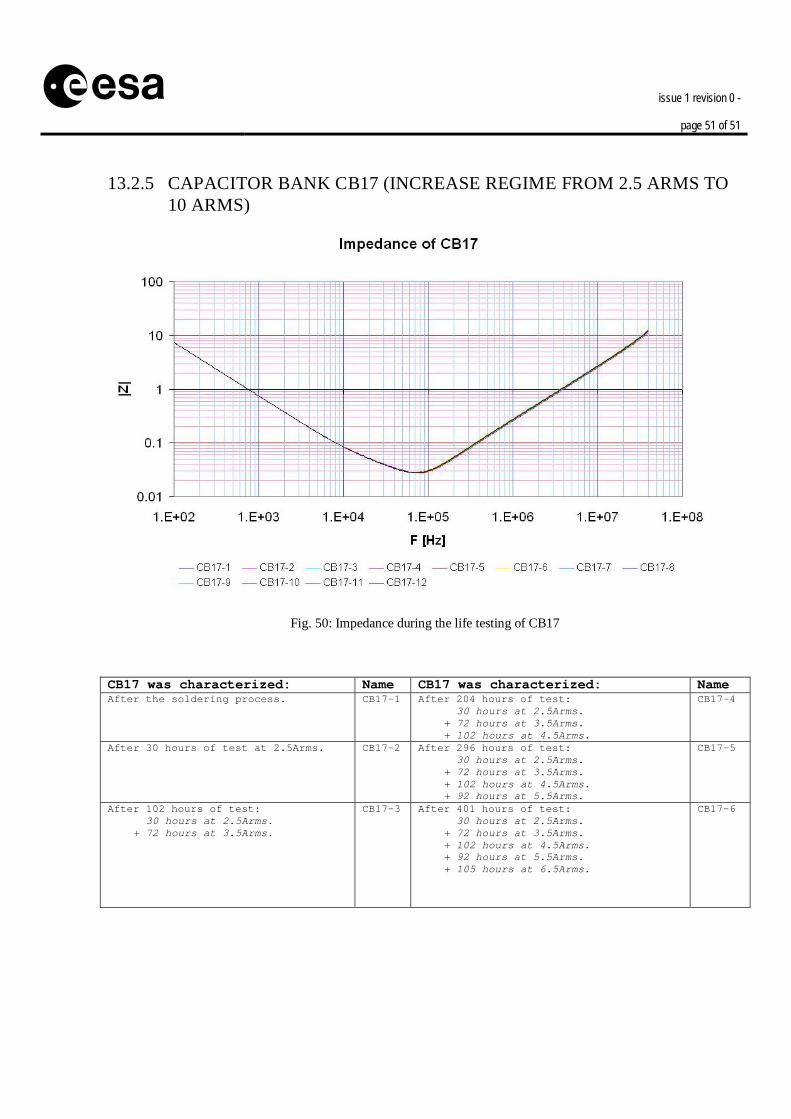
issue 1 revision 0 -
page 51 of 51
s
13.2.5 CAPACITOR BANK CB17 (INCREASE REGIME FROM 2.5 ARMS TO 10 ARMS)
Fig. 50: Impedance during the life testing of CB17
CB17 was characterized: Name CB17 was characterized: Name After the soldering process. CB17-1 After 204 hours of test:
30 hours at 2.5Arms. + 72 hours at 3.5Arms. + 102 hours at 4.5Arms.
CB17-4
After 30 hours of test at 2.5Arms. CB17-2 After 296 hours of test: 30 hours at 2.5Arms. + 72 hours at 3.5Arms. + 102 hours at 4.5Arms. + 92 hours at 5.5Arms.
CB17-5
After 102 hours of test: 30 hours at 2.5Arms. + 72 hours at 3.5Arms.
CB17-3 After 401 hours of test: 30 hours at 2.5Arms. + 72 hours at 3.5Arms. + 102 hours at 4.5Arms. + 92 hours at 5.5Arms. + 105 hours at 6.5Arms.
CB17-6

issue 1 revision 0 -
page 52 of 52
s After 506 hours of test: 30 hours at 2.5Arms. + 72 hours at 3.5Arms. + 102 hours at 4.5Arms. + 92 hours at 5.5Arms. + 105 hours at 6.5Arms. + 105 hours at 7.5Arms.
CB17-7 After 718 hours of test: 30 hours at 2.5Arms. + 72 hours at 3.5Arms. + 102 hours at 4.5Arms. + 92 hours at 5.5Arms. + 105 hours at 6.5Arms. + 105 hours at 7.5Arms. + 104 hours at 8.5Arms. + 108 hours at 8.5Arms + 97 hours at 8.5Arms
CB17-10
After 610 hours of test: 30 hours at 2.5Arms. + 72 hours at 3.5Arms. + 102 hours at 4.5Arms. + 92 hours at 5.5Arms. + 105 hours at 6.5Arms. + 105 hours at 7.5Arms. + 104 hours at 8.5Arms.
CB17-8 After 718 hours of test: 30 hours at 2.5Arms. + 72 hours at 3.5Arms. + 102 hours at 4.5Arms. + 92 hours at 5.5Arms. + 105 hours at 6.5Arms. + 105 hours at 7.5Arms. + 104 hours at 8.5Arms. + 108 hours at 8.5Arms + 97 hours at 8.5Arms + 77 hours at 8.5 Arms
CB17-11
After 718 hours of test: 30 hours at 2.5Arms. + 72 hours at 3.5Arms. + 102 hours at 4.5Arms. + 92 hours at 5.5Arms. + 105 hours at 6.5Arms. + 105 hours at 7.5Arms. + 104 hours at 8.5Arms. + 108 hours at 8.5Arms.
CB17-9 After 718 hours of test: 30 hours at 2.5Arms. + 72 hours at 3.5Arms. + 102 hours at 4.5Arms. + 92 hours at 5.5Arms. + 105 hours at 6.5Arms. + 105 hours at 7.5Arms. + 104 hours at 8.5Arms. + 108 hours at 8.5Arms + 97 hours at 8.5Arms + 77 hours at 8.5Arms + 78 hours at 10Arms -> Total 972 hours
CB17-12
Analysis of the results: The capacitance of the capacitor banks remains the same (low frequency part). It seems that the ESL of the capacitor banks changed slightly (high frequency part). This variation may be essentially due to differences in the position of the capacitor bank, when it is connected to the frequency analyzer. Analysis of the results: The impedance of this capacitor bank remains the same during all the tests.

issue 1 revision 0 -
page 53 of 53
s
14 CONCLUSION In absence of detailed impedance data, the calculation of the maximum current expected on each capacitor in a bank is an issue and the relevant reliability too. In the part 6.2, two methods were presented to help tantalum capacitor users checking if their design respects the ratings/de-ratings rules. No failure was observed during the parallel configuration tests. The impedances remained the same throughout the tests. The leakage current of one capacitor bank showed appreciable changes but still remaining lower than the maximum specified in the manufacturer datasheet. The presented tests were performed on only a few capacitors, and for this reason any generalization of the results of this study should be taken with great care. The effects of the soldering process on capacitors long-term reliability was not part of this study but it may have an impact on the performances of the tantalum capacitors and on the explanation of the failures occurred in ESA programs. The study of the influences of the soldering process on the performances of tantalum capacitors should be object of a next investigation.

issue 1 revision 0 -
page 54 of 54
s
15 ANNEXES
15.1 Annex 1: Determination of the maximum RMS current in a TAJ (K RHJ) 10uF 35V case D
Single configuration Method of the manufacturer with the typical ESR Assuming to apply a square current waveform with duty cycle=0.5, the RMS current at 25°C has to be lower than 1 A RMS to respect the rated power dissipation for that package (150mW) by using the typical ESR values in function of frequency at 25°C provided by AVX.
TypicalI amplitude Fs Harmonics F Amplitude of the Harmonic I I*I ESR P
[A] [Hz] [] [Hz] [A] [RMSA] [Ohms] [W]
1.00 130000 1 130000 1.270441417 0.898337741 0.807010697 0.1621 1.31E-013 390000 0.423480472 0.299445914 0.089667855 0.1194 1.07E-025 650000 0.254088283 0.179667548 0.032280428 0.1043 3.37E-037 910000 0.181491631 0.128333963 0.016469606 0.09801 1.61E-039 1170000 0.141160157 0.099815305 0.009963095 0.0945 9.42E-04
11 1430000 0.115494674 0.081667067 0.00666951 0.09209 6.14E-0413 1690000 0.097726263 0.069102903 0.004775211 0.09025 4.31E-0415 1950000 0.084696094 0.059889183 0.003586714 0.08876 3.18E-0417 2210000 0.074731848 0.052843397 0.002792425 0.08753 2.44E-04
PI 19 2470000 0.066865338 0.047280934 0.002235487 0.0865 1.93E-043.14159265 21 2730000 0.06049721 0.042777988 0.001829956 0.08564 1.57E-04
23 2990000 0.055236583 0.039058163 0.00152554 0.08492 1.30E-0425 3250000 0.050817657 0.03593351 0.001291217 0.08431 1.09E-0427 3510000 0.047053386 0.033271768 0.001107011 0.0838 9.28E-0529 3770000 0.043808325 0.030977163 0.000959585 0.08337 8.00E-0531 4030000 0.040981981 0.028978637 0.000839761 0.083 6.97E-0533 4290000 0.038498225 0.027222356 0.000741057 0.0827 6.13E-0535 4550000 0.036298326 0.025666793 0.000658784 0.08244 5.43E-05
sqrt of sumsq 0.992171325
Fig. 51: manufacturer method to obtain the maximum rms current with the typical ESR Maximum RMS current via the maximum ESR given by the manufacturer The maximum of the real part of the impedance (ESR max is specified in the datasheet) can be used to determine the power dissipation. Rated Pd (150mW) is achieved for a the square wave current with 50% duty cycle equal to 0.39 A RMS with a considered series resistor of 1Ω.

issue 1 revision 0 -
page 55 of 55
s Typica l
I amplitude Fs Harmonics F Amplitude of the Harmonic I I*I ESR P Total P[A] [Hz] [] [Hz] [A] [RMSA] [Ohms] [W] [W]
0.39 130000 1 130000 0.495921512 0.350669464 0.122969073 1 1.23E-01 1.50E-013 390000 0.165307171 0.116889821 0.01366323 1 1.37E-025 650000 0.099184302 0.070133893 0.004918763 1 4.92E-037 910000 0.07084593 0.050095638 0.002509573 1 2.51E-039 1170000 0.05510239 0.038963274 0.001518137 1 1.52E-03
11 1430000 0.045083774 0.031879042 0.001016273 1 1.02E-0313 1690000 0.038147809 0.026974574 0.000727628 1 7.28E-0415 1950000 0.033061434 0.023377964 0.000546529 1 5.47E-0417 2210000 0.029171854 0.020627616 0.000425499 1 4.25E-04
PI 19 2470000 0.026101132 0.018456288 0.000340635 1 3.41E-043.14159265 21 2730000 0.02361531 0.016698546 0.000278841 1 2.79E-04
23 2990000 0.021561805 0.015246498 0.000232456 1 2.32E-0425 3250000 0.01983686 0.014026779 0.000196751 1 1.97E-0427 3510000 0.018367463 0.012987758 0.000168682 1 1.69E-0429 3770000 0.017100742 0.01209205 0.000146218 1 1.46E-0431 4030000 0.015997468 0.011311918 0.000127959 1 1.28E-0433 4290000 0.015027925 0.010626347 0.000112919 1 1.13E-0435 4550000 0.014169186 0.010019128 0.000100383 1 1.00E-04
sqrt of sumsq 0.387297751
Fig. 52: method to obtain the maximum rms current with the maximum ESR
Maximum RMS current after the measure of the single impedance With the frequency analyser the impedance of the single capacitor is measured at 25°C. Assuming to apply a square current waveform with duty cycle=0.5, the current waveform applied to the capacitor is decomposed in Fourier series. It is then possible to calculate the RMS power dissipation at each harmonic with the measured impedance. Root-square sum of the individual harmonic contributions gives the RMS power dissipation for one capacitor after characterization. The RMS current at 25°C has to be lower than 0.74 A RMS to respect the rated power dissipation for that package (150mW) by using the measured impedance at 25°C.
Typica lI amplitude Fs Harmonics F Amplitude of the Harmonic I I*I ESR P Total P
[A] [Hz] [] [Hz] [A] [RMSA] [Ohms] [W] [W]
0.74 130000 1 130000 0.937840163 0.663153139 0.439772086 0.294 1.29E-01 1.50E-013 390000 0.312613388 0.221051046 0.048863565 0.229 1.12E-025 650000 0.187568033 0.132630628 0.017590883 0.21 3.69E-037 910000 0.133977166 0.094736163 0.008974941 0.2 1.79E-039 1170000 0.104204463 0.073683682 0.005429285 0.194 1.05E-03
11 1430000 0.085258197 0.060286649 0.00363448 0.191 6.94E-0413 1690000 0.072141551 0.05101178 0.002602202 0.189 4.92E-0415 1950000 0.062522678 0.044210209 0.001954543 0.187 3.65E-0417 2210000 0.055167068 0.039009008 0.001521703 0.187 2.85E-04
PI 19 2470000 0.049360009 0.034902797 0.001218205 0.186 2.27E-043.14159265 21 2730000 0.044659055 0.031578721 0.000997216 0.186 1.85E-04
23 2990000 0.040775659 0.028832745 0.000831327 0.186 1.55E-0425 3250000 0.037513607 0.026526126 0.000703635 0.186 1.31E-0427 3510000 0.034734821 0.024561227 0.000603254 0.187 1.13E-0429 3770000 0.032339316 0.02286735 0.000522916 0.187 9.78E-0531 4030000 0.030252908 0.021392037 0.000457619 0.188 8.60E-0533 4290000 0.028419399 0.02009555 0.000403831 0.188 7.59E-0535 4550000 0.026795433 0.018947233 0.000358998 0.189 6.79E-05
sqrt of sumsq 0.732421114
Fig. 53: method to obtain the maximum rms current with a measured ESR of one capacitor

issue 1 revision 0 -
page 56 of 56
s
15.2 Annex 2: Determination of the maximum RMS current in a TPS (M R0200) 22uF 35V case D
Single configuration Method of the manufacturer with the typical ESR Assuming to apply a square current waveform with duty cycle=0.5, the RMS current at 25°C has to be lower than 1.19 A RMS to respect the rated power dissipation for that package (150mW) by using the typical ESR values in function of frequency at 25°C provided by AVX.
Typica lI amplitude Fs Harmonics F Amplitude of the Harmonic I I*I ESR P Total P
[A] [Hz] [] [Hz] [A] [RMSA] [Ohms] [W] [W]
1.20 130000 1 130000 1.528410709 1.080749577 1.168019648 0.1112 1.30E-01 1.50E-013 390000 0.509470236 0.360249859 0.129779961 0.08236 1.07E-025 650000 0.305682142 0.216149915 0.046720786 0.0775 3.62E-037 910000 0.218344387 0.154392797 0.023837136 0.07521 1.79E-039 1170000 0.169823412 0.120083286 0.014419996 0.0736 1.06E-03
11 1430000 0.138946428 0.098249962 0.009653055 0.07235 6.98E-0413 1690000 0.117570055 0.083134583 0.006911359 0.07136 4.93E-0415 1950000 0.101894047 0.072049972 0.005191198 0.07057 3.66E-0417 2210000 0.089906512 0.063573505 0.00404159 0.06994 2.83E-04
PI 19 2470000 0.080442669 0.056881557 0.003235511 0.06944 2.25E-043.14159265 21 2730000 0.072781462 0.051464266 0.002648571 0.06905 1.83E-04
23 2990000 0.06645264 0.046989112 0.002207977 0.06874 1.52E-0425 3250000 0.061136428 0.043229983 0.001868831 0.06849 1.28E-0427 3510000 0.056607804 0.040027762 0.001602222 0.06829 1.09E-0429 3770000 0.052703818 0.037267227 0.001388846 0.06814 9.46E-0531 4030000 0.049303571 0.03486289 0.001215421 0.06802 8.27E-0533 4290000 0.046315476 0.032749987 0.001072562 0.06792 7.28E-0535 4550000 0.043668877 0.030878559 0.000953485 0.06785 6.47E-05
sqrt of sumsq 1.193636525
Fig. 54: manufacturer method to obtain the maximum rms current with the typical ESR Maximum RMS current via the maximum ESR given by the manufacturer The maximum of the real part of the impedance (ESR max is specified in the datasheet) can be used to determine the power dissipation. Rated Pd (150mW) is achieved for a the square wave current with 50% duty cycle equal to 0.87 A RMS with a considered series resistor of 0.2Ω.
Typica lI amplitude Fs Harmonics F Amplitude of the Harmonic I I*I ESR P Total P
[A] [Hz] [] [Hz] [A] [RMSA] [Ohms] [W] [W]
0.87 130000 1 130000 1.108914266 0.784120797 0.614845425 0.2 1.23E-01 1.50E-013 390000 0.369638089 0.261373599 0.068316158 0.2 1.37E-025 650000 0.221782853 0.156824159 0.024593817 0.2 4.92E-037 910000 0.158416324 0.112017257 0.012547866 0.2 2.51E-039 1170000 0.123212696 0.087124533 0.007590684 0.2 1.52E-03
11 1430000 0.100810388 0.071283709 0.005081367 0.2 1.02E-0313 1690000 0.085301097 0.060316984 0.003638139 0.2 7.28E-0415 1950000 0.073927618 0.05227472 0.002732646 0.2 5.47E-0417 2210000 0.065230251 0.046124753 0.002127493 0.2 4.25E-04
PI 19 2470000 0.058363909 0.041269516 0.001703173 0.2 3.41E-043.14159265 21 2730000 0.052805441 0.037339086 0.001394207 0.2 2.79E-04
23 2990000 0.048213664 0.034092209 0.001162279 0.2 2.32E-0425 3250000 0.044356571 0.031364832 0.000983753 0.2 1.97E-0427 3510000 0.041070899 0.029041511 0.000843409 0.2 1.69E-0429 3770000 0.038238423 0.027038648 0.000731088 0.2 1.46E-0431 4030000 0.035771428 0.025294219 0.000639798 0.2 1.28E-0433 4290000 0.033603463 0.023761236 0.000564596 0.2 1.13E-0435 4550000 0.031683265 0.022403451 0.000501915 0.2 1.00E-04
sqrt of sumsq 0.866024141
Fig. 55: method to obtain the maximum rms current with the maximum ESR

issue 1 revision 0 -
page 57 of 57
s Maximum RMS current after the measure of the single impedance With the frequency analyser the impedance of the single capacitor is measured at 25°C. Assuming to apply a square current waveform with duty cycle=0.5, the current waveform applied to the capacitor is decomposed in Fourier series. It is then possible to calculate the typical RMS power dissipation at each harmonic with the measured impedance. Root-square sum of the individual harmonic contributions gives the RMS power dissipation for one capacitor after characterization. The RMS current at 25°C has to be lower than 0.91 A RMS to respect the rated power dissipation for that package (150mW) by using the measured impedance at 25°C.
Typica lI amplitude Fs Harmonics F Amplitude of the Harmonic I I*I ESR P Total P
[A] [Hz] [] [Hz] [A] [RMSA] [Ohms] [W] [W]
0.91 130000 1 130000 1.162028231 0.821678042 0.675154805 0.191 1.29E-01 1.50E-013 390000 0.387342744 0.273892681 0.075017201 0.149 1.12E-025 650000 0.232405646 0.164335608 0.027006192 0.138 3.73E-037 910000 0.166004033 0.117382577 0.013778669 0.134 1.85E-039 1170000 0.129114248 0.09129756 0.008335245 0.132 1.10E-03
11 1430000 0.10563893 0.074698004 0.005579792 0.131 7.31E-0413 1690000 0.089386787 0.063206003 0.003994999 0.13 5.19E-0415 1950000 0.077468549 0.054778536 0.003000688 0.13 3.90E-0417 2210000 0.068354602 0.048334002 0.002336176 0.13 3.04E-04
PI 19 2470000 0.061159381 0.043246213 0.001870235 0.132 2.47E-043.14159265 21 2730000 0.055334678 0.039127526 0.001530963 0.132 2.02E-04
23 2990000 0.050522967 0.035725132 0.001276285 0.1325 1.69E-0425 3250000 0.046481129 0.032867122 0.001080248 0.1335 1.44E-0427 3510000 0.043038083 0.03043252 0.000926138 0.134 1.24E-0429 3770000 0.040069939 0.028333726 0.0008028 0.1345 1.08E-0431 4030000 0.037484782 0.026505743 0.000702554 0.1355 9.52E-0533 4290000 0.035212977 0.024899335 0.000619977 0.137 8.49E-0535 4550000 0.033200807 0.023476515 0.000551147 0.1375 7.58E-05
sqrt of sumsq 0.907504332
Fig. 56: method to obtain the maximum rms current with a measured ESR of a capacitor

issue 1 revision 0 -
page 58 of 58
s
15.3 Annex 3: Determination of the maximum RMS current in a TPS (K R0300) 10uF 35V case D
Single configuration Method of the manufacturer with the typical ESR Assuming to apply a square current waveform with duty cycle=0.5, the RMS current at 25°C has to be lower than 0.9 A RMS to respect the rated power dissipation for that package (150mW).
Typica lI amplitude Fs Harmonics F Amplitude of the Harmonic I I*I ESR P Total P
[A] [Hz] [] [Hz] [A] [RMSA] [Ohms] [W] [W]
0.91 130000 1 130000 1.155573694 0.817113995 0.667675282 0.1153 7.70E-02 1.50E-013 390000 0.385191231 0.272371332 0.074186142 0.9154 6.79E-025 650000 0.231114739 0.163422799 0.026707011 0.07784 2.08E-037 910000 0.165081956 0.116730571 0.013626026 0.07133 9.72E-049 1170000 0.128397077 0.090790444 0.008242905 0.06783 5.59E-04
11 1430000 0.105052154 0.07428309 0.005517978 0.06565 3.62E-0413 1690000 0.088890284 0.062854923 0.003950741 0.06411 2.53E-0415 1950000 0.077038246 0.054474266 0.002967446 0.06293 1.87E-0417 2210000 0.067974923 0.048065529 0.002310295 0.06197 1.43E-04
PI 19 2470000 0.060819668 0.043006 0.001849516 0.06117 1.13E-043.14159265 21 2730000 0.055027319 0.03891019 0.001514003 0.06047 9.16E-05
23 2990000 0.050242335 0.035526695 0.001262146 0.05987 7.56E-0525 3250000 0.046222948 0.03268456 0.00106828 0.05935 6.34E-0527 3510000 0.042799026 0.030263481 0.000915878 0.05889 5.39E-0529 3770000 0.039847369 0.028176345 0.000793906 0.05849 4.64E-0531 4030000 0.037276571 0.026358516 0.000694771 0.05814 4.04E-0533 4290000 0.035017385 0.02476103 0.000613109 0.05783 3.55E-0535 4550000 0.033016391 0.023346114 0.000545041 0.05756 3.14E-05
sqrt of sumsq 0.90246356
Fig. 57: manufacturer method to obtain the maximum rms current with the typical ESR Maximum RMS current via the maximum ESR given by the manufacturer Maximum ESR from the datasheet: ESRmax=0.3Ω (at 100Khz) Rated Pd (150mW) is achieved for a square wave current equal to 0.71 A RMS.
Typica lI amplitude Fs Harmonics F Amplitude of the Harmonic I I*I ESR P Total P
[A] [Hz] [] [Hz] [A] [RMSA] [Ohms] [W] [W]
0.71 130000 1 130000 0.905423601 0.640231168 0.409895949 0.3 1.23E-01 1.50E-013 390000 0.301807867 0.213410389 0.045543994 0.3 1.37E-025 650000 0.18108472 0.128046234 0.016395838 0.3 4.92E-037 910000 0.129346229 0.091461595 0.008365223 0.3 2.51E-039 1170000 0.100602622 0.071136796 0.005060444 0.3 1.52E-03
11 1430000 0.082311236 0.058202833 0.00338757 0.3 1.02E-0313 1690000 0.069647969 0.049248551 0.00242542 0.3 7.28E-0415 1950000 0.060361573 0.042682078 0.00182176 0.3 5.47E-0417 2210000 0.053260212 0.037660657 0.001418325 0.3 4.25E-04
PI 19 2470000 0.047653874 0.033696377 0.001135446 0.3 3.41E-043.14159265 21 2730000 0.04311541 0.030487198 0.000929469 0.3 2.79E-04
23 2990000 0.039366244 0.027836138 0.000774851 0.3 2.32E-0425 3250000 0.036216944 0.025609247 0.000655834 0.3 1.97E-0427 3510000 0.033534207 0.023712265 0.000562272 0.3 1.69E-0429 3770000 0.031221503 0.022076937 0.000487391 0.3 1.46E-0431 4030000 0.029207213 0.020652618 0.000426531 0.3 1.28E-0433 4290000 0.027437079 0.019400944 0.000376397 0.3 1.13E-0435 4550000 0.025869246 0.018292319 0.000334609 0.3 1.00E-04
sqrt of sumsq 0.707104887
Fig. 57: method to obtain the maximum rms current with the maximum ESR

issue 1 revision 0 -
page 59 of 59
s Maximum RMS current after the measure of the single impedance With the frequency analyser the impedance of the single capacitor is measured at 25°C. Assuming to apply a square current waveform with duty cycle=0.5, the current waveform applied to the capacitor is decomposed in Fourier series. It is then possible to calculate the typical RMS power dissipation at each harmonic with the measured impedance. Root-square sum of the individual harmonic contributions gives the RMS power dissipation for one capacitor after characterization. The RMS current at 25°C has to be lower than 0.93 A RMS to respect the rated power dissipation for that package (150mW) by using the measured impedance at 25°C.
Typica lI amplitude Fs Harmonics F Amplitude of the Harmonic I I*I ESR P Total P
[A] [Hz] [] [Hz] [A] [RMSA] [Ohms] [W] [W]
0.93 130000 1 130000 1.18781194 0.839909878 0.705448603 0.101 7.13E-02 8.24E-023 390000 0.395937313 0.279969959 0.078383178 0.08 6.27E-035 650000 0.237562388 0.167981976 0.028217944 0.07 1.98E-037 910000 0.16968742 0.119987125 0.01439691 0.065 9.36E-049 1170000 0.131979104 0.09332332 0.008709242 0.0615 5.36E-04
11 1430000 0.107982904 0.076355443 0.005830154 0.0595 3.47E-0413 1690000 0.091370149 0.064608452 0.004174252 0.0579 2.42E-0415 1950000 0.079187463 0.055993992 0.003135327 0.057 1.79E-0417 2210000 0.069871291 0.049406463 0.002440999 0.056 1.37E-04
PI 19 2470000 0.062516418 0.044205783 0.001954151 0.0553 1.08E-043.14159265 21 2730000 0.056562473 0.039995708 0.001599657 0.055 8.80E-05
23 2990000 0.051643997 0.036517821 0.001333551 0.0546 7.28E-0525 3250000 0.047512478 0.033596395 0.001128718 0.0545 6.15E-0527 3510000 0.043993035 0.031107773 0.000967694 0.0542 5.24E-0529 3770000 0.040959032 0.02896241 0.000838821 0.0541 4.54E-0531 4030000 0.038316514 0.027093867 0.000734078 0.054 3.96E-0533 4290000 0.035994301 0.025451814 0.000647795 0.054 3.50E-0535 4550000 0.033937484 0.023997425 0.000575876 0.054 3.11E-05
sqrt of sumsq 0.927640528
Fig. 58: method to obtain the maximum rms current with a measured ESR of a capacitor

issue 1 revision 0 -
page 60 of 60
s
15.4 Annex 4: impedances, ESRs, and X of TAJD 22uF 35V
Impedance of C1-C10
0.01
0.1
1
10
100
100 1000 10000 100000 1000000 10000000 100000000F [Hz]
|Z|
C2 C3 C1 C4 C5 C6 C7 C8 C9 C10 typical
+
ESR=f(F) C1-C10
0.01
0.1
1
10
100 1000 10000 100000 1000000 10000000 100000000F [Hz]
ESR
[Ohm
s]
ESR-C1 Typical ESR-C2 ESR-C3 ESR-C4 ESR-C5 ESR-C6 ESR-C7 ESR-C8 ESR-C9 ESR-C10 X=f(F) C1-C10
-3.6E-05
-2.6E-05
-1.6E-05
-6.0E-06
4.0E-06
1.4E-05
2.4E-05
3.4E-05
100 1000 10000 100000 1000000 10000000F [Hz]
X [F
]
Typical X-C1 X-C2 X-C3 X-C4 X-C5 X-C6 X-C7 X-C8 X-C9 X-C10
Fig 59a b and c: Impedances, ESRs and Capacitances of 10 capacitors (C1-C10) TAJD 22uF 35V

issue 1 revision 0 -
page 61 of 61
s
Impedance of C11-C20
0.01
0.1
1
10
100
100 1000 10000 100000 1000000 10000000 100000000
F [Hz]
|Z|
C12 C13 C11 C14 C15 C16 C17 C18 C19 C20 typical
ESR=f(F) C11-C20
0.01
0.1
1
10
100 1000 10000 100000 1000000 10000000 100000000F [Hz]
ESR
[Ohm
s]
ESR-C11 Typical ESR-C12 ESR-C13 ESR-C14 ESR-C15 ESR-C16 ESR-C17 ESR-C18ESR-C19 ESR-C20
X=f(F) C11-C20
-3.6E-05
-2.6E-05
-1.6E-05
-6.0E-06
4.0E-06
1.4E-05
2.4E-05
3.4E-05
100 1000 10000 100000 1000000 10000000F [Hz]
X [F
]
Typical X-C11 X-C12 X-C13 X-C14 X-C15 X-C16 X-C17 X-C18 X-C19 X-C20 Fig 60a, b and c: Impedances, Esr and capacitances of 10 capacitors (C11-C20) TAJD 22uF 35V

issue 1 revision 0 -
page 62 of 62
s Impedance of C21-C30
0.01
0.1
1
10
100
100 1000 10000 100000 1000000 10000000 100000000
F [Hz]
|Z|
C22 C23 C21 C24 C25 C26 C27 C28 C29 C30 typical ESR=f(F) C21-C30
0.01
0.1
1
10
100 1000 10000 100000 1000000 10000000 100000000
F [Hz]
ESR
[Ohm
s]
ESR-C21 Typical ESR-C22 ESR-C23 ESR-C24 ESR-C25 ESR-C26 ESR-C27 ESR-C28ESR-C29 ESR-C30
X=f(F) C21-C30
-3.6E-05
-2.6E-05
-1.6E-05
-6.0E-06
4.0E-06
1.4E-05
2.4E-05
3.4E-05
100 1000 10000 100000 1000000 10000000F [Hz]
X [F
]
Typical X-C21 X-C22 X-C23 X-C24 X-C25 X-C26 X-C27 X-C28 X-C29 X-C30
Fig 61 a, b and c: Impedances, Esr and capacitances of 10 capacitors (C21-C30) TAJD 22uF 35V
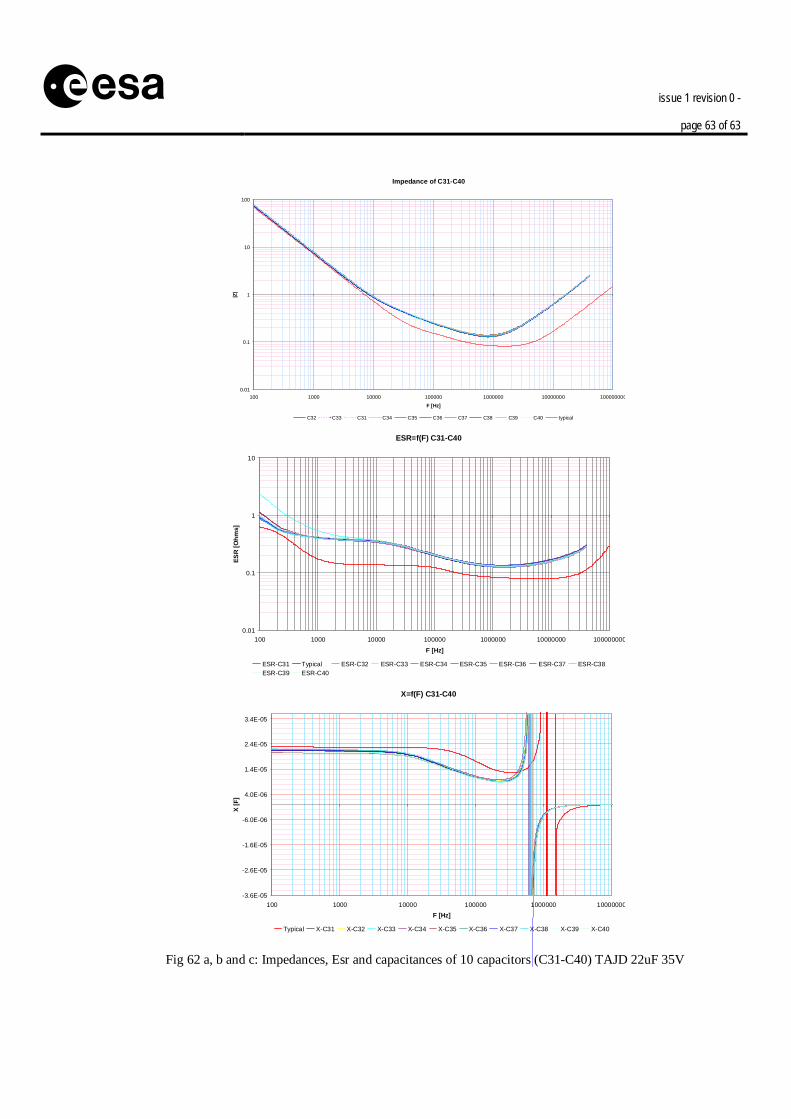
issue 1 revision 0 -
page 63 of 63
s
Impedance of C31-C40
0.01
0.1
1
10
100
100 1000 10000 100000 1000000 10000000 100000000
F [Hz]
|Z|
C32 C33 C31 C34 C35 C36 C37 C38 C39 C40 typical ESR=f(F) C31-C40
0.01
0.1
1
10
100 1000 10000 100000 1000000 10000000 100000000
F [Hz]
ESR
[Ohm
s]
ESR-C31 Typical ESR-C32 ESR-C33 ESR-C34 ESR-C35 ESR-C36 ESR-C37 ESR-C38ESR-C39 ESR-C40
X=f(F) C31-C40
-3.6E-05
-2.6E-05
-1.6E-05
-6.0E-06
4.0E-06
1.4E-05
2.4E-05
3.4E-05
100 1000 10000 100000 1000000 10000000F [Hz]
X [F
]
Typical X-C31 X-C32 X-C33 X-C34 X-C35 X-C36 X-C37 X-C38 X-C39 X-C40
Fig 62 a, b and c: Impedances, Esr and capacitances of 10 capacitors (C31-C40) TAJD 22uF 35V

issue 1 revision 0 -
page 64 of 64
s
Impedance of C41-C50
0.01
0.1
1
10
100
100 1000 10000 100000 1000000 10000000 100000000
F [Hz]
|Z|
C42 C43 C41 C44 C45 C46 C47 C48 C49 C50 typical ESR=f(F) C41-C50
0.01
0.1
1
10
100 1000 10000 100000 1000000 10000000 100000000
F [Hz]
ESR
[Ohm
s]
ESR-C41 Typical ESR-C42 ESR-C43 ESR-C44 ESR-C45 ESR-C46 ESR-C47 ESR-C48ESR-C49 ESR-C50
X=f(F) C41-C50
-3.6E-05
-2.6E-05
-1.6E-05
-6.0E-06
4.0E-06
1.4E-05
2.4E-05
3.4E-05
100 1000 10000 100000 1000000 10000000F [Hz]
X [F
]
Typical X-C41 X-C42 X-C43 X-C44 X-C45 X-C46 X-C47 X-C48 X-C49 X-C50
Fig 63 a, b and c: Impedances, Esr and capacitances of 10 capacitors (C41-C50) TAJD 22uF 35V

issue 1 revision 0 -
page 65 of 65
s 15.5 Annex 5: impedances, ESRs, and X of TAJD 10uF 35V
Impedance of B1-B10
0.01
0.1
1
10
100
1000
100 1000 10000 100000 1000000 10000000 100000000
F [Hz]
|Z|
B2 B3 B1 B4 B5 B6 B7 B8 B9 B10 Typical ESR=f(F) of B1-B10
0.01
0.1
1
10
100 1000 10000 100000 1000000 10000000 100000000
F [Hz]
ESR
B2 B3 B1 B4 B5 B6 B7 B8 B9 B10 Typical X=f(F) of B1-B10
-1.50E-05
-5.00E-06
5.00E-06
1.50E-05
100 1000 10000 100000 1000000 10000000 100000000
F [Hz]
X
B2 B3 B1 B4 B5 B6 B7 B8 B9 B10 Typical Fig 64 a, b and c: Impedances, ESRs and Capacitances of 10 capacitors (B1-B10) TAJD 10uF 35V

issue 1 revision 0 -
page 66 of 66
s
Impedance of B11-B20
0.01
0.1
1
10
100
1000
100 1000 10000 100000 1000000 10000000 100000000
F [Hz]
|Z|
B12 B13 B11 B14 B15 B16 B17 B18 B19 B20 Typical
ESR=f(F) of B11-B20
0.01
0.1
1
10
100 1000 10000 100000 1000000 10000000 100000000
F [Hz]
ESR
B12 B13 B11 B14 B15 B16 B17 B18 B19 B20 Typical X=f(F) of B11-B20
-1.50E-05
-5.00E-06
5.00E-06
1.50E-05
100 1000 10000 100000 1000000 10000000 100000000
F [Hz]
X
B12 B13 B11 B14 B15 B16 B17 B18 B19 B20 Typical Fig 65 a, b and c: Impedances, ESRs and Capacitances of 10 capacitors (B21-B30) TAJD 10uF 35V

issue 1 revision 0 -
page 67 of 67
s Impedance of B21-B30
0.01
0.1
1
10
100
1000
100 1000 10000 100000 1000000 10000000 100000000
F [Hz]
|Z|
B22 B23 B21 B24 B25 B26 B27 B28 B29 B30 Typical
ESR=f(F) of B21-B30
0.01
0.1
1
10
100 1000 10000 100000 1000000 10000000 100000000
F [Hz]
ESR
B22 B23 B21 B24 B25 B26 B27 B28 B29 B30 Typical X=f(F) of B21-B30
-1.50E-05
-5.00E-06
5.00E-06
1.50E-05
100 1000 10000 100000 1000000 10000000 100000000
F [Hz]
X
B22 B23 B21 B24 B25 B26 B27 B28 B29 B30 Typical Fig 66a, b and c: Impedances, ESRs and Capacitances of 10 capacitors (B21-B30) TAJD 10uF 35V

issue 1 revision 0 -
page 68 of 68
s Impedance of B31-B40
0.01
0.1
1
10
100
1000
100 1000 10000 100000 1000000 10000000 100000000
F [Hz]
|Z|
B32 B33 B31 B34 B35 B36 B37 B38 B39 B40 Typical
ESR=f(F) of B31-B40
0.01
0.1
1
10
100 1000 10000 100000 1000000 10000000 100000000
F [Hz]
ESR
B32 B33 B31 B34 B35 B36 B37 B38 B39 B40 Typical
X=f(F) of B31-B40
-1.50E-05
-5.00E-06
5.00E-06
1.50E-05
100 1000 10000 100000 1000000 10000000 100000000
F [Hz]
X
B32 B33 B31 B34 B35 B36 B37 B38 B39 B40 Typical
Fig 67 a, b and c: Impedances, ESRs and Capacitances of 10 capacitors (B31-B40) TAJD 10uF 35V

issue 1 revision 0 -
page 69 of 69
s Impedance of B41-B50
0.01
0.1
1
10
100
1000
100 1000 10000 100000 1000000 10000000 100000000
F [Hz]
|Z|
B42 B43 B41 B44 B45 B46 B47 B48 B49 B50 Typical
ESR=f(F) of B41-B50
0.01
0.1
1
10
100 1000 10000 100000 1000000 10000000 100000000
F [Hz]
ESR
B42 B43 B41 B44 B45 B46 B47 B48 B49 B50 Typical X=f(F) of B41-B50
-1.50E-05
-5.00E-06
5.00E-06
1.50E-05
100 1000 10000 100000 1000000 10000000 100000000
F [Hz]
X
B42 B43 B41 B44 B45 B46 B47 B48 B49 B50 Typical
Fig 68 a, b and c: Impedances, ESRs and Capacitances of 10 capacitors (B41-B50) TAJD 10uF 35V

issue 1 revision 0 -
page 70 of 70
s 15.6 Annex 6: Comparisons of the impedance before and after the
soldering process for Capacitor banks (CB13 to CB17) of TAJD 22uF 35V (C1 to C50)
Note that the graphs of the capacitor bank impedances obtained before the test results is calculated from the parallelization of the capacitors tested individually; the graphs of the capacitor bank impedances obtained after the test results is measured from the capacitor banks after the soldering. The differences of the impedances are mainly due to the additional parasitic resistances and inductances of the PCB and the solder joints.
Impedance of CB13 (Reference CB)
0.01
0.1
1
10
100
100 1000 10000 100000 1000000 10000000 100000000
F [Hz]
|Z|
CB13 after soldering process C1//C2//C3//C4//C5//C6//C7//C8//C9//C10 Fig. 69: Comparisons of the impedances of CB13 before and after the soldering process for the TAJD 22uF 35V

issue 1 revision 0 -
page 71 of 71
s
Impedance of CB14
0.01
0.1
1
10
100
100 1000 10000 100000 1000000 10000000 100000000
F [Hz]
|Z|
CB14 after soldering process C1i// Fig. 70: Comparisons of the impedances of CB14 before and after the soldering process for the TAJD 22uF 35V
Impedance of CB15
0.01
0.1
1
10
100
100 1000 10000 100000 1000000 10000000 100000000
F [Hz]
|Z|
CB15 after soldering process C2i // Fig. 71: Comparisons of the impedances of CB15 before and after the soldering process for the TAJD 22uF 35V
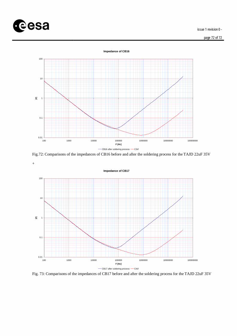
issue 1 revision 0 -
page 72 of 72
s Impedance of CB16
0.01
0.1
1
10
100
100 1000 10000 100000 1000000 10000000 100000000
F [Hz]
|Z|
CB16 after soldering process C3i// Fig.72: Comparisons of the impedances of CB16 before and after the soldering process for the TAJD 22uF 35V +
Impedance of CB17
0.01
0.1
1
10
100
100 1000 10000 100000 1000000 10000000 100000000
F [Hz]
|Z|
CB17 after soldering process C4i// Fig. 73: Comparisons of the impedances of CB17 before and after the soldering process for the TAJD 22uF 35V

issue 1 revision 0 -
page 73 of 73
s
15.7 Annex 7: Comparisons of the impedance before and after the soldering process for Capacitor banks (CB7 to CB11) of TAJD 10uF 35V (B1 to B50)
Note that the graphs of the capacitor bank impedances obtained before the test results is calculated from the parallelization of the capacitors tested individually; the graphs of the capacitor bank impedances obtained after the test results is measured from the capacitor banks after the soldering. The differences of the impedances are mainly due to the additional parasitic resistances and inductances of the PCB and the solder joints.
Impedance of CB7
0.01
0.1
1
10
100
100 1000 10000 100000 1000000 10000000 100000000
F [Hz]
IZI
Cii// CB7 after soldering process Fig. 74: Comparisons of the impedances of CB7 before and after the soldering process for the TAJD 10uF 35V (B1...B10)

issue 1 revision 0 -
page 74 of 74
s Impedance of CB8
0.01
0.1
1
10
100
100 1000 10000 100000 1000000 10000000 100000000
F [Hz]
|Z|
Bi// After soldering process Fig. 75: Comparisons of the impedances of CB8 before and after the soldering process for the TAJD 10uF 35V (B11...B20)
Impedance of CB9
0.01
0.1
1
10
100
100 1000 10000 100000 1000000 10000000 100000000
F [Hz]
|Z|
Bi// After soldering process Fig. 76: Comparisons of the impedances of CB9 before and after the soldering process for the TAJD 10uF 35V (B21...B30)

issue 1 revision 0 -
page 75 of 75
s Impedance of CB10
0.01
0.1
1
10
100
100 1000 10000 100000 1000000 10000000 100000000
F [Hz]
|Z|
Bi// After the soldering process Fig. 77: Comparisons of the impedances of CB10 before and after the soldering process for the TAJD 10uF 35V (B31...B40)
Impedance of CB11
0.01
0.1
1
10
100
100 1000 10000 100000 1000000 10000000 100000000
F [Hz]
|Z|
Bi// After the soldering process Fig. 78: Comparisons of the impedances of CB11 before and after the soldering process for the TAJD 10uF 35V (B41...B50)

issue 1 revision 0 -
page 76 of 76
s
15.8 Annex 8: Heating plates System
Fig. 79a and b: Aluminium plate to heat the capacitor bank to 85degC
Fig. 80: Power part of the heating plate
The circuit shown in Fig 81 controls the MFETs. Please note that the figure 81 presents only the circuit used to control one MFET. The same circuit is duplicated to control the second MFET. This precaution allows having two autonomous control circuits.

issue 1 revision 0 -
page 77 of 77
s The heart of the temperature control card is a LM335. This device is a temperature sensor, which is connecting on the resistors side of the heating plate. It is supplied by a constant current (#1mA) with the intermediate current mirror build with Q1 and Q2 (part 1 of the fig. 81). The signal from the temperature sensor is an image of the temperature. This signal is filtered via a differential amplifier, designed with an operational amplifier Lm124 (part 2 of fig. 81). The filtered signal from the differential amplifier is then compared to a reference voltage with a Schmidt trigger (provided with a very small hysteresis to avoid the oscillating control of the MFET). When the temperature is higher than the programmed threshold, then the signal from the differential amplifier exceeds the temperature voltage reference and the gate of the MFET is close to zero (the current in the heating resistors is switched-off until the temperature signal from the differential amplifier reached the temperature voltage reference of the Schmidt trigger). Which this simple control principle it is possible to control the temperature of the capacitors at 85 degC +/-2degC.
Fig. 81: Schematic of the temperature control card of the heating plate.
Related Documents