Texas Instruments Texas Instruments System Power Design for Wall-Powered Application Dec, 18 th - 22 th , 2006 Kevin Lin HPA Asia Market Development

Welcome message from author
This document is posted to help you gain knowledge. Please leave a comment to let me know what you think about it! Share it to your friends and learn new things together.
Transcript
Texas InstrumentsTexas Instruments
System Power Design for Wall-Powered Application
Dec, 18th - 22th, 2006Kevin Lin
HPA Asia Market Development
2
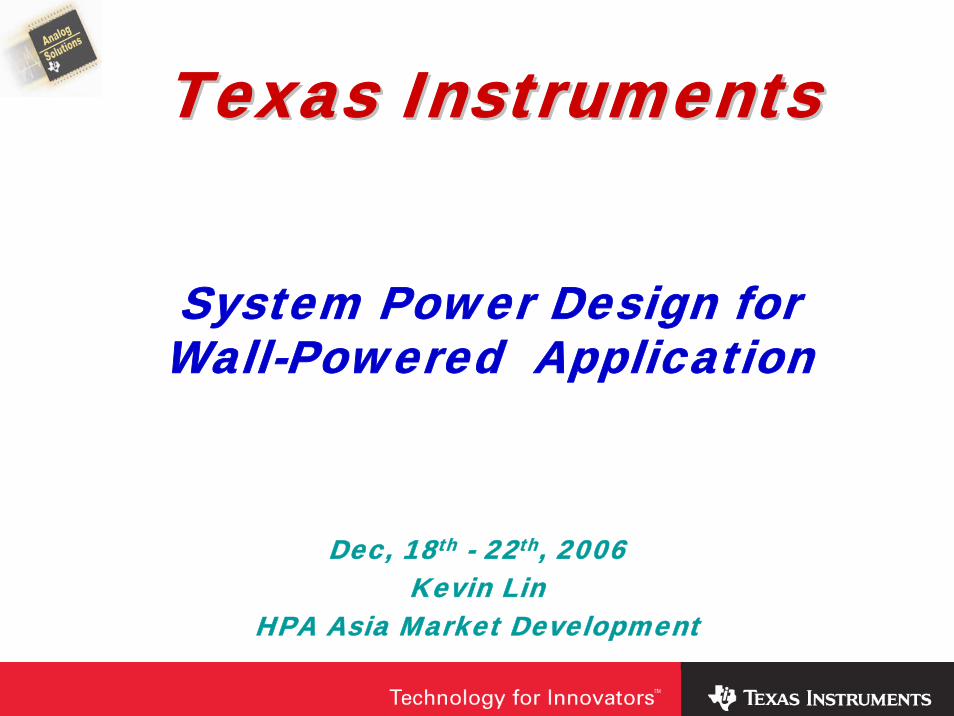
Utility AC LineUtility AC Line--Powered SystemsPowered Systems
Portfolio Strength in...Portfolio Strength in...AC/DC, isolated DC/DC Power factor correctionPoint-of-load DC/DCPlug-in power modulesHot swap/PoEPower distributionFET gate driveDigital power
Full System Solutions
IndustrialIndustrial
CommunicationCommunication
ComputingComputing
ConsumerConsumer

3
Texas Instruments Power HistoryTexas Instruments Power History
TI has Built the leading Power Management Business
ContentContent
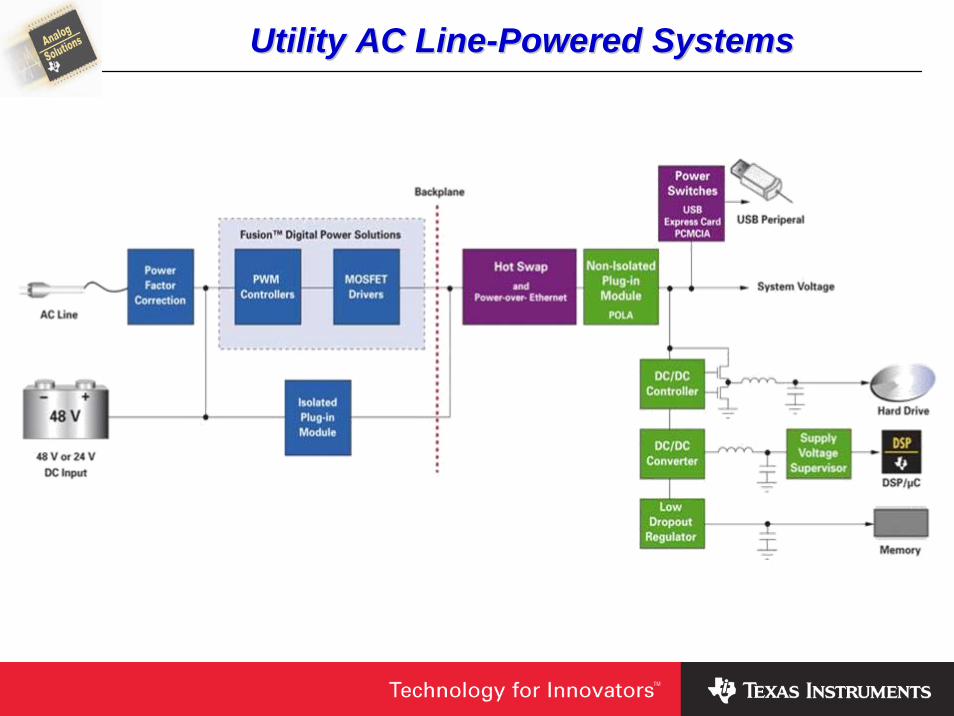
ACAC--DC PFC DC PFC IntroductionIntroduction & Design Considerations& Design Considerations
Isolated PWM SolutionsIsolated PWM Solutions IntroductionIntroduction
DCDC--DC Buck DC Buck Design Software IntroductionDesign Software Introduction
5
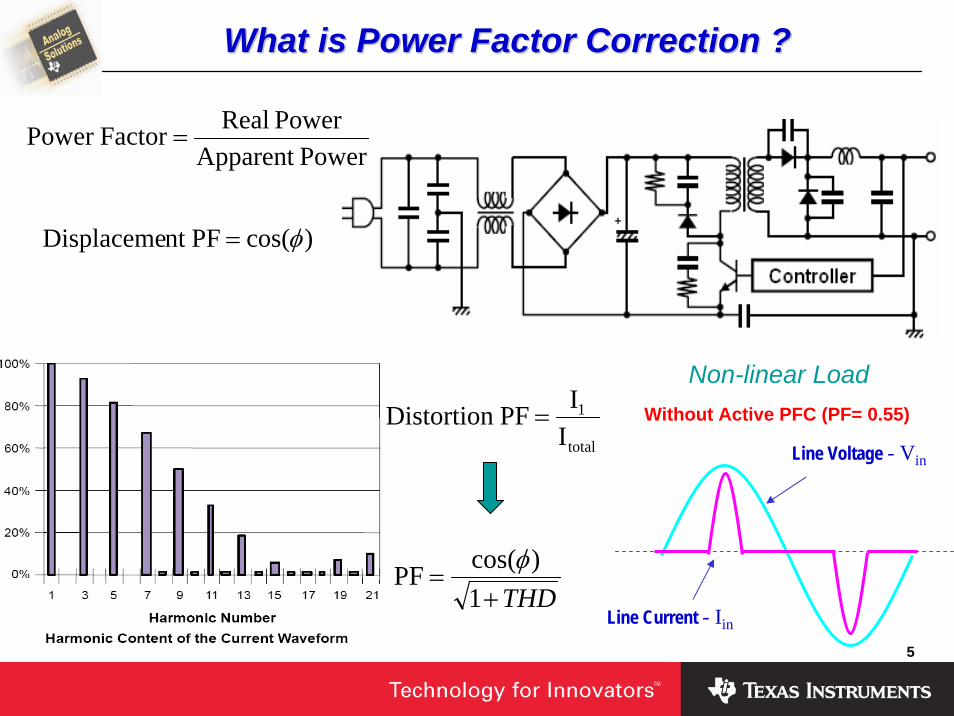
What is What is Power Factor Correction Power Factor Correction ??
Line Voltage - Vin
Line Current - Iin
Without Active PFC (PF= 0.55)
Non-linear Load
Line Voltage - Vin
Line Current - Iin
Without Active PFC (PF= 0.80)
Linear Load
)cos(PFnt Displaceme φ=
total
1
IIPF Distortion =
THD+=
1)cos(PF φ
PowerApparent Power RealFactorPower =

6
Benefits for PBenefits for PFCFC CircuitsCircuits
Power Factor Correction is Widely Used
Increases Current Available from LineReduces 3rd Harmonic DistortionEuropean Market Requirement
• EN 61000-3-2 is following standard
Enables Universal Line Operation w/o Mech-Switches• No need for switches to handle 120V vs... 240V line voltage
Easier to Meet Hold-up Time Requirements• Energy is stored at a higher voltage of bulk capacitor
Can make Second Stage Design Easier
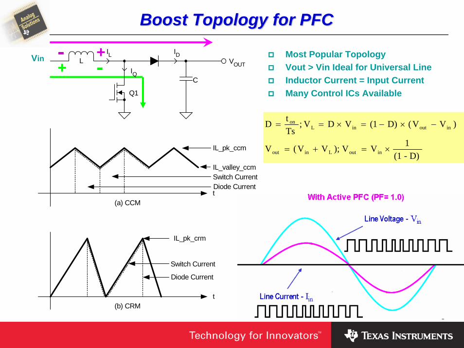
Line Voltage - Vin
Line Current - Iin
Without Active PFC (PF= 0.55)
With Active PFC (PF= 1.0)
Look at Available System Power:Assume 15A Breaker, 98% η Rectifier, PF=0.55 (Typical Rectifier w/o PFC)
P = 120 Vrms • 15 A • 0.55 • 0.98 = 970 WIf PF = 0.99 Available Power = 1746 W
Increases “Available” Line Power of 80%
7
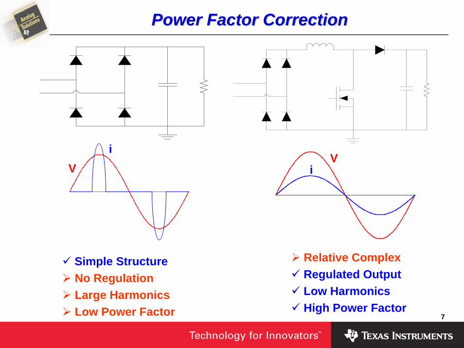
Power Factor CorrectionPower Factor Correction
Simple StructureNo RegulationLarge HarmonicsLow Power Factor
Vi
Relative ComplexRegulated OutputLow HarmonicsHigh Power Factor
Vi
8
Vin -+ -
+
D)-(11VV);VV(V
)VV(D)1(VDV;TstD
inoutLinout
inoutinLon
×=+=
−×−=×==
Boost Topology for PFCBoost Topology for PFC
t(a) CCM
t(b) CRM
Diode Current
Switch Current
Diode CurrentSwitch Current
IL_pk_ccm
IL_valley_ccm
C
VOUTL
Q1
IL ID
IQ
IL_pk_crm
Most Popular TopologyVout > Vin Ideal for Universal Line Inductor Current = Input CurrentMany Control ICs Available

9
PFC Design ConsiderationsPFC Design Considerations
Trade-Off in between Performance and Total System Cost Optimum control method – Average Current Mode (ACM) Simpler inexpensive control – Transition Mode or Critical Mode (DCM)High-efficiency & performance – Zero Voltage Transition Mode (ZVT)
To Meet System Operation RequirementHigher PF and lower THD features – input current harmonics shall comply with IEC 61000-3-2.PFC bulk capacitor design – hold up time; Iripple & voltage ratingAppropriate DC filtering capacitor – bypass current ripple noisePower sequencing techniques for PFC & PWM stagesSafety and EMI requirements (conduction & radiation)
System-Board Space & Development Time LimitationLayout & placement issue – guideline Thermal dissipation management
Stability and ReliabilityProtection features (OVP, SCP, UVP, OCP, OTP)
10
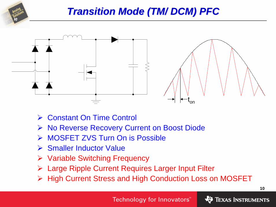
Transition Mode (TM/ DCM) PFCTransition Mode (TM/ DCM) PFC
Constant On Time ControlNo Reverse Recovery Current on Boost DiodeMOSFET ZVS Turn On is PossibleSmaller Inductor ValueVariable Switching FrequencyLarge Ripple Current Requires Larger Input FilterHigh Current Stress and High Conduction Loss on MOSFET
ton
11
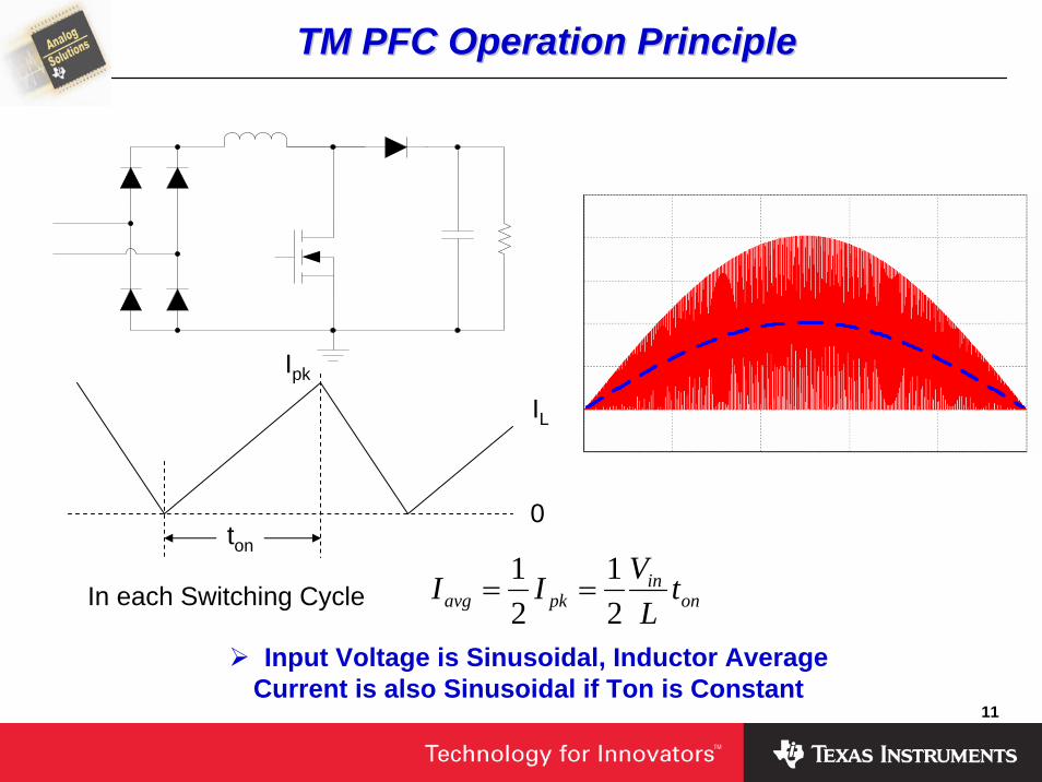
TM PFC Operation PrincipleTM PFC Operation Principle
0
IL
In each Switching Cycle onin
pkavg tL
VII21
21
==
Input Voltage is Sinusoidal, Inductor Average Current is also Sinusoidal if Ton is Constant
ton
Ipk

12
Switching Performance EstimationSwitching Performance Estimation
Because of Resonance between Boost Inductor and MOSFET Junction Capacitor, Less Turn on Loss can be Realized
ZVS can be Achieved if Input Voltage is Less than Half of the Output Voltage
Less Turn On Loss is Expected Comparing with CCM Mode
IL
Vds
Because of Transition Mode Operation, No Reverse Recovery LossLow cost, Standard Diode can be Used
Vds
IL

13
+–
R IMO
GATEDRIVE
+–
C O
LOAD
R I
R FC Z
C P
TEXT+–
IMPROVEDNOISE
IMMUNITY
PWMV S
Q1
IMO
V INI IN
IINR SENSE
– +
ACLINE
IAC
LPF
MULTK M
SQUAREK G
DIVK D
E/A
E/AN
D
V VAV REF
L IN
ID1 V O IO
V O
V FF
D1
Real Current Waveform
Input Voltage Sine Waveform
Input Feed Forward
Output Bus Voltage
Current Follow & Commend
Regulation & Constant Power
PWM Commend
UCC3818A UCC3818A -- 16 Pin CCM PFC Controller16 Pin CCM PFC Controller
Real Current Waveform
Input Voltage Sine Waveform
Input Feed Forward
Output Bus Voltage
Current Follow & Commend
Regulation & Constant Power
PWM Command
14
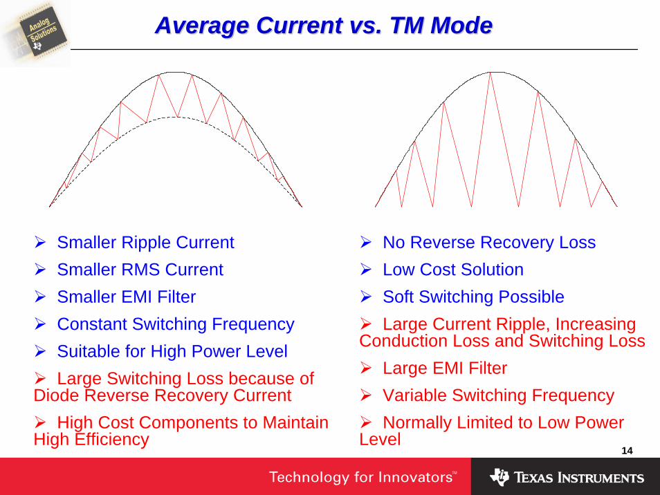
Average Current vs. TM Mode Average Current vs. TM Mode
Smaller Ripple CurrentSmaller RMS CurrentSmaller EMI FilterConstant Switching FrequencySuitable for High Power LevelLarge Switching Loss because of
Diode Reverse Recovery CurrentHigh Cost Components to Maintain
High Efficiency
No Reverse Recovery LossLow Cost SolutionSoft Switching PossibleLarge Current Ripple, Increasing
Conduction Loss and Switching LossLarge EMI FilterVariable Switching FrequencyNormally Limited to Low Power
Level
15
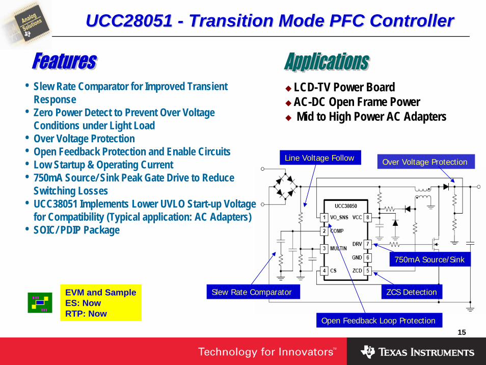
LCD-TV Power BoardAC-DC Open Frame PowerMid to High Power AC Adapters
• Slew Rate Comparator for Improved Transient Response
• Zero Power Detect to Prevent Over Voltage Conditions under Light Load
• Over Voltage Protection• Open Feedback Protection and Enable Circuits• Low Startup & Operating Current• 750mA Source/ Sink Peak Gate Drive to Reduce
Switching Losses• UCC38051 Implements Lower UVLO Start-up Voltage
for Compatibility (Typical application: AC Adapters)• SOIC/ PDIP Package
EVM and SampleES: NowRTP: Now
UCUCCC28051 28051 -- Transition Mode PFC ControllerTransition Mode PFC Controller
Slew Rate Comparator
Over Voltage ProtectionLine Voltage Follow
Open Feedback Loop Protection
750mA Source/Sink
ZCS Detection
16
UCUC22853853AA -- 8 Pin CCM (ACM) PFC Controller8 Pin CCM (ACM) PFC Controller
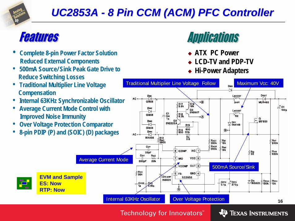
ATX PC PowerLCD-TV and PDP-TVHi-Power Adapters
• Complete 8-pin Power Factor SolutionReduced External Components
• 500mA Source/ Sink Peak Gate Drive toReduce Switching Losses
• Traditional Multiplier Line Voltage Compensation
• Internal 63KHz Synchronizable Oscillator• Average Current Mode Control with
Improved Noise Immunity• Over Voltage Protection Comparator• 8-pin PDIP (P) and (SOIC) (D) packages
Internal 63KHz Oscillator Over Voltage Protection
Traditional Multiplier Line Voltage Follow
Average Current Mode 500mA Source/Sink
Maximum Vcc: 40V
EVM and SampleES: NowRTP: Now
17
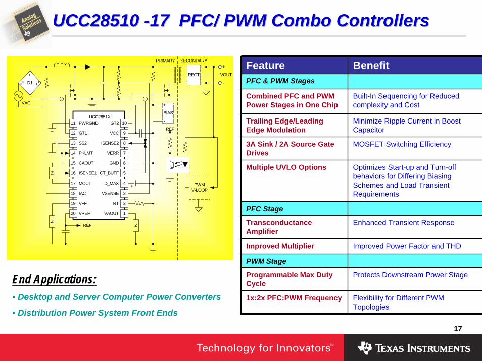
UCC28510UCC28510 --17 PFC/ PWM Comb17 PFC/ PWM Comboo ControllersControllers
12
3
16
18
10
5
7
2
UCC2851X
GT1
VSENSE
ISENSE1
IAC
GT2
VREF
VERR
RT
+–
D1
VAC
15
14
13
11
17
19
20
PWRGND
VAOUT 1
6
VFF
MOUT
CAOUT
PKLMT
SS2 8
9
D_MAX
CT_BUFF
GND
ISENSE2
VCC
REF
PRIMARY SECONDARY+
-VOUT
+4
REF
BIAS
RECT
+
-
PWMV-LOOP
Z
ZZ
End Applications:• Desktop and Server Computer Power Converters
• Distribution Power System Front Ends
Feature BenefitPFC & PWM Stages
Trailing Edge/Leading Edge Modulation
Minimize Ripple Current in Boost Capacitor
3A Sink / 2A Source Gate Drives
MOSFET Switching Efficiency
TransconductanceAmplifier
Enhanced Transient Response
Multiple UVLO Options Optimizes Start-up and Turn-off behaviors for Differing Biasing Schemes and Load Transient Requirements
PFC Stage
Improved Multiplier Improved Power Factor and THD
Programmable Max Duty Cycle
Protects Downstream Power Stage
1x:2x PFC:PWM Frequency Flexibility for Different PWM Topologies
PWM Stage
Combined PFC and PWM Power Stages in One Chip
Built-In Sequencing for Reduced complexity and Cost

18
Power Factor Correction ControllersPower Factor Correction Controllers
Avg. I-Mode
Transition Mode
ZVT
Specialized PFC Controllers
Zero Voltage Switching PFC (Telecom Rectifiers, >1kW High Power)
PFC+PWM Combination Controllers (Desktops, Flyback, Boost)
General Purpose Average Current Mode CCM PFC
Transition Mode or Boundary Mode (Adapters, Lighting Ballasts)
UCC28050/51Improved Transient
Resp., Industry Std. Pinout
UC2853A8-pin CCM<65KHZ
UC3855A/BZVT, Higher Frequency
UCC38500-03PFC+PWM, LEM/TEM
UCC28510-17PFC+PWM, LEM/TEM,
Prog.MaxDC
UCC3819/ATracking
Boost PFC
UCC3817/18; UCC3817A/18A
BiCMOS UC3854A, LEM
UCC28018/198-pin CCM
PFC
UCC28018/198-pin CCM
PFCUC3854A/BImproved
16-pin CCM
Existing Products 2007+
UCC28070Interleaved CCM PFC
UCC28070Interleaved CCM PFC
UCC28060Interleaved TM
PFC
UCC28060Interleaved TM
PFC
UCC28521UCC28528PFC+PWM, TEM/TEM,
Prog.MaxDC
19
ACAC--DC PFC DC PFC IntroductionIntroduction & Design Considerations& Design Considerations
Isolated PWM Solutions IntroductionIsolated PWM Solutions Introduction
DCDC--DC Buck Design Software IntroductionDC Buck Design Software Introduction
20
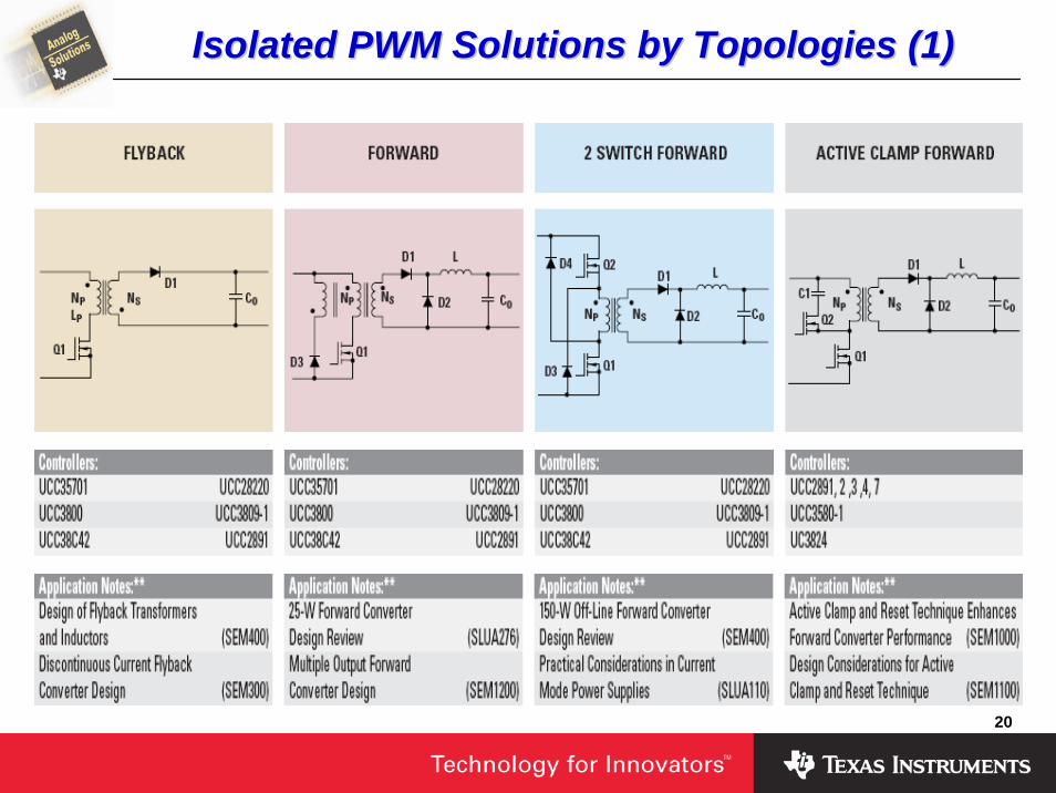
Isolated PWM Solutions by Topologies (1)Isolated PWM Solutions by Topologies (1)
21
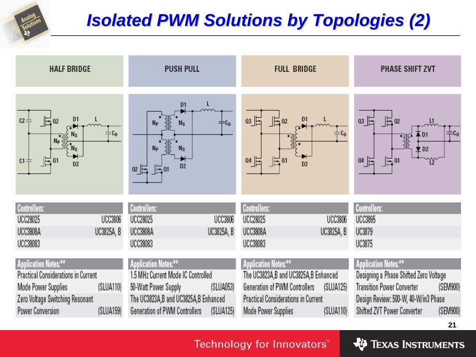
Isolated PWM Solutions by Topologies (2)Isolated PWM Solutions by Topologies (2)
22
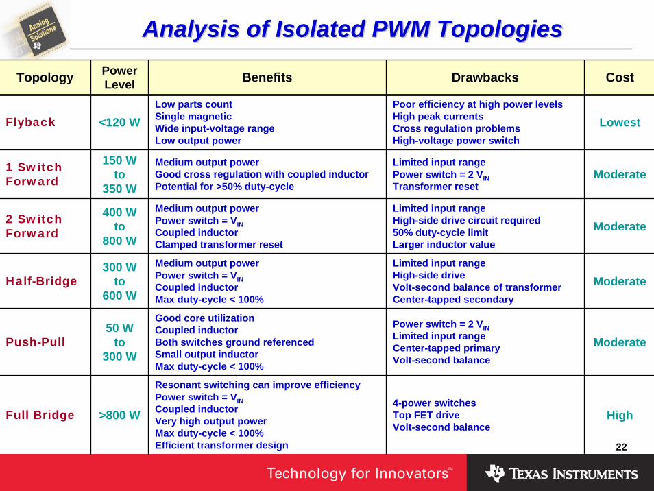
Topology Power Level Benefits Drawbacks Cost
Flyback <120 WLow parts countSingle magneticWide input-voltage rangeLow output power
Poor efficiency at high power levelsHigh peak currentsCross regulation problemsHigh-voltage power switch
Lowest
1 Switch Forward
150 Wto
350 W
Medium output powerGood cross regulation with coupled inductorPotential for >50% duty-cycle
Limited input rangePower switch = 2 VINTransformer reset
Moderate
2 Switch Forward
400 Wto
800 W
Medium output powerPower switch = VINCoupled inductorClamped transformer reset
Limited input rangeHigh-side drive circuit required50% duty-cycle limitLarger inductor value
Moderate
Half-Bridge300 W
to600 W
Medium output powerPower switch = VINCoupled inductorMax duty-cycle < 100%
Limited input rangeHigh-side driveVolt-second balance of transformerCenter-tapped secondary
Moderate
Push-Pull50 W
to300 W
Good core utilizationCoupled inductorBoth switches ground referencedSmall output inductorMax duty-cycle < 100%
Power switch = 2 VINLimited input rangeCenter-tapped primary Volt-second balance
Moderate
Full Bridge >800 W
Resonant switching can improve efficiencyPower switch = VINCoupled inductor Very high output powerMax duty-cycle < 100%Efficient transformer design
4-power switchesTop FET driveVolt-second balance
High
Analysis of Isolated PWM TopologiesAnalysis of Isolated PWM Topologies
23
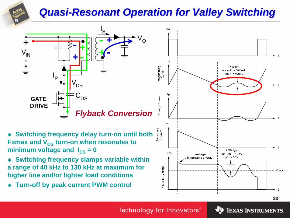
Switching frequency delay turn-on until both Fsmax and VDS turn-on when resonates to minimum voltage and IDS = 0
Switching frequency clamps variable within a range of 40 kHz to 130 kHz at maximum for higher line and/or lighter load conditions
Turn-off by peak current PWM control
IMAG
IPRI
t
t
t
VDS
t
VIN
ISEC
t
∼ LMAG CDS
Leakage Inductance energy
VGS
N x VO
CDSGATEDRIVE
IS
IP VDS
+VIN-
VO
QuasiQuasi--Resonant Operation for Valley SwitchingResonant Operation for Valley Switching
+-
-+ -
++-
Flyback Conversion
24
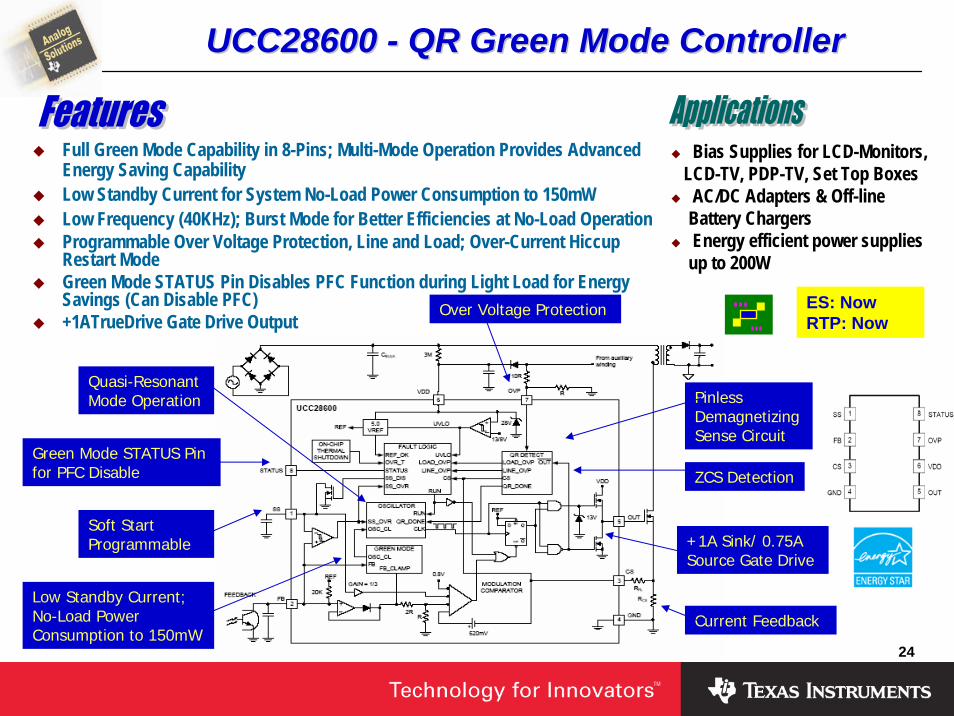
UCC28600 UCC28600 -- QR Green Mode ControllerQR Green Mode Controller
Full Green Mode Capability in 8-Pins; Multi-Mode Operation Provides Advanced Energy Saving CapabilityLow Standby Current for System No-Load Power Consumption to 150mWLow Frequency (40KHz); Burst Mode for Better Efficiencies at No-Load Operation Programmable Over Voltage Protection, Line and Load; Over-Current Hiccup Restart ModeGreen Mode STATUS Pin Disables PFC Function during Light Load for Energy Savings (Can Disable PFC)+1ATrueDrive Gate Drive Output
Green Mode STATUS Pin for PFC Disable
Over Voltage Protection
Quasi-Resonant Mode Operation
Low Standby Current; No-Load Power Consumption to 150mW
+1A Sink/ 0.75A Source Gate Drive
ZCS Detection
PinlessDemagnetizing Sense Circuit
Soft Start Programmable
Current Feedback
Bias Supplies for LCD-Monitors, LCD-TV, PDP-TV, Set Top Boxes
AC/DC Adapters & Off-line Battery ChargersEnergy efficient power supplies up to 200W
ES: NowRTP: Now
25
Applicable to Forward and Flyback TopologiesActive Clamp Applied to Either High Side or Low Side
Advantages– Natural ZVS (Zero Voltage Switching) for Highest Efficiency– >50% Duty Cycle– Recycles Inductive Energy– Reduced EMI– Easy to Adapt Self-Driven Synchronous Rectification
Disadvantages– Additional MOSFET Switch Required for Active Reset– Gate Drive Circuitry somewhat Complex– Precision Max Duty Cycle Clamp is Critical– Advanced PWM Control Technique Required
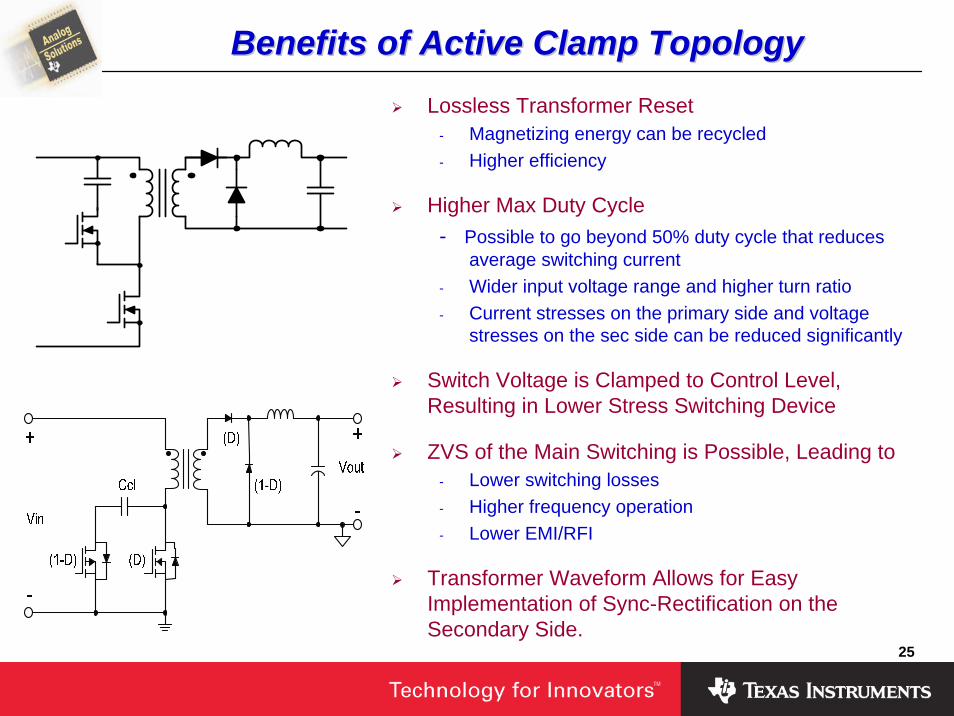
Benefits of Active Clamp TopologyBenefits of Active Clamp TopologyLossless Transformer Reset
- Magnetizing energy can be recycled - Higher efficiency
Higher Max Duty Cycle - Possible to go beyond 50% duty cycle that reduces
average switching current- Wider input voltage range and higher turn ratio- Current stresses on the primary side and voltage
stresses on the sec side can be reduced significantly
Switch Voltage is Clamped to Control Level, Resulting in Lower Stress Switching Device
ZVS of the Main Switching is Possible, Leading to- Lower switching losses - Higher frequency operation- Lower EMI/RFI
Transformer Waveform Allows for Easy Implementation of Sync-Rectification on the Secondary Side.
26
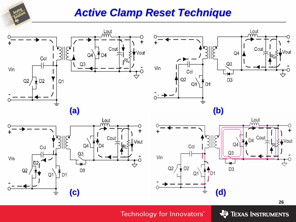
Active Clamp Reset TechniqueActive Clamp Reset Technique
(a)(a)
(c)(c)
(b)(b)
(d)(d)
27
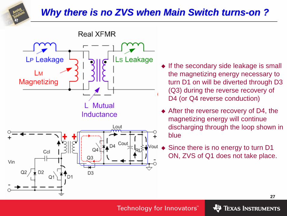
Why there is no ZVS when Main Switch turnsWhy there is no ZVS when Main Switch turns--on ?on ?
If the secondary side leakage is small the magnetizing energy necessary to turn D1 on will be diverted through D3 (Q3) during the reverse recovery of D4 (or Q4 reverse conduction)
After the reverse recovery of D4, the magnetizing energy will continue discharging through the loop shown in blue
Since there is no energy to turn D1 ON, ZVS of Q1 does not take place.

28
UCC2891/2/3/4/7 UCC2891/2/3/4/7 –– Active Clamp ControllersActive Clamp Controllers
Product ControlGate Drive
(Sink/Source)
HV Startup Circuit
SYNCLINE
MonitorAuxiliary
Output
CS1 Thres-hold
CS2 Thres-hold
Slope Comp
Max. Osc. Freq.
UCC2891 CMC±2A
TrueDrive™
(110V) (UV)P-Ch 0.75V - 1MHz
UCC2892 CMC±2A
TrueDrive™ - (UV,OV)
P-Ch 1.27V - 1MHz
UCC2893 CMC±2A
TrueDrive™
(110V) (UV)N-Ch 0.75V - 1MHz
UCC2894 CMC±2A
TrueDrive™ - (UV,OV)
N-Ch 1.27V - 1MHz
UCC2897 CMC±2A
TrueDrive™
(110V)
(Bi-dir)
(UV,OV) P-Ch 0.5V 0.75V 1MHz
UCC3580 VMC +1A / -0.5A - - P-Ch or N-Ch
- - N/A 400kHz
Performance / Efficiency:– ±2-A TrueDrive™ Gate
Drives
Flexibility:– Telecom bus compatible
Built-in 110V Start-up Circuit
– Prog. Internal Slope Comp– Bidirectional Oscillator
Synchronization– -40°C to +125°C Operation
Protection:– Incorporates 0.5V Cycle by
Cycle Current Limit – 0.75V Second Level Hiccup
Mode Threshold– Accurate Input Line UV and
OV Protection Monitors

29
PWM Controllers (50W PWM Controllers (50W ––>1KW)>1KW)
Existing Products 2006+
Soft-Switching, ZVT, ZVS (Phase-Shifted Full-Bridge, Resonant, Active-Clamp Forward)
Dual- Complementary Outputs (Push-Pull, Half-Bridge, Full Bridge, Current-Fed/Voltage-Fed Push-Pull, Two Independent Flybacks/Forwards)
General Purpose Single Ended PWM(Forward, Flyback, Buck, Boost, SEPIC, Cuk)
Secondary Side Control; Post Regulation(Forward, Buck, Synchronous Buck)
Green-Mode PWM and Off-line Bias Regulators(Flyback, Forward, QR Flyback)
UCC3580V-Mode
Act-Clamp
UC3861-8Resonant Mode
Controllers
UCC3895Adv. Φ-Shift
UC3875-8w/ Drivers
UC3879w/o Drivers
UC3524AUC3525AUC3526A
UC3846UC3856
UC3825A/B
UC3825
UCC3806
UCC3808/A8-pin P-P
UCC38083-6+Slope CompUC28025
UCC28220/1Interleaved
Fwd/FlybackProg MaxDC >50%
UC3849Avg.I-Mode
w/ LS
UC3824UCC3839
Avg.I-Mode
UCC3960/61Primary Side
Start-up
UC3827I/V-Fed P-P
UCC2891-4I-Mode Act-
Clamp, HVStart
UCC3580SR Control
UCC3583UC3854SSPR
UCC38102 Independent
Channels, ≤50%DC
UCC2541Sec. Side Sync-Buck
w/ Osc., PGD™
UCC2541Sec. Side Sync-Buck
w/ Osc., PGD™
UCC2897Adv. I-Mode Act-Clamp,
HVStart
UCC2540Sec. Side Sync-
Buck, PGD™
UC3827I/V-Fed P-P
UCC28089Push-Pull Osc
UC3842-5UC3842A-5A
UCC3800-5UCC3813
4/5Vref, SS, LEB
UCC3884Freq. Foldback,
V*S ClampUCC38C42-45
BiCMOS 3842A-45A
UCC3807UCC3809
Prog. Max DC
UCC3888/89Off-line BiasRegulators
UCC28600QR Green Mode PWM
UCC28600QR Green Mode PWMUCC3581
Micro PowerGreen PWM
Voltage Mode
Current Mode
Resonant Mode
ACAC--DC PFC DC PFC IntroductionIntroduction & Design Considerations& Design Considerations
Isolated PWM Solutions IntroductionIsolated PWM Solutions Introduction
DCDC--DC Buck Design Software IntroductionDC Buck Design Software Introduction
31
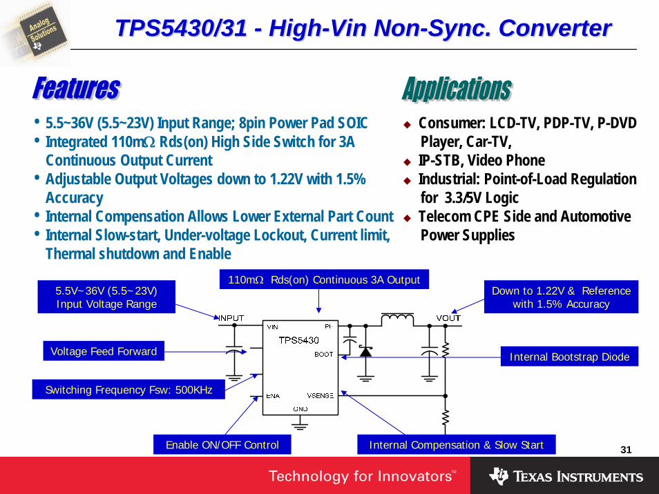
TPS5430/31 TPS5430/31 -- HighHigh--VinVin NonNon--Sync. ConverterSync. Converter
Consumer: LCD-TV, PDP-TV, P-DVD Player, Car-TV, IP-STB, Video Phone Industrial: Point-of-Load Regulation for 3.3/5V LogicTelecom CPE Side and AutomotivePower Supplies
• 5.5~36V (5.5~23V) Input Range; 8pin Power Pad SOIC• Integrated 110mΩ Rds(on) High Side Switch for 3A
Continuous Output Current• Adjustable Output Voltages down to 1.22V with 1.5%
Accuracy• Internal Compensation Allows Lower External Part Count• Internal Slow-start, Under-voltage Lockout, Current limit,
Thermal shutdown and Enable
Enable ON/OFF Control
110mΩ Rds(on) Continuous 3A Output5.5V~36V (5.5~23V) Input Voltage Range
Internal Compensation & Slow Start
Down to 1.22V & Reference with 1.5% Accuracy
Switching Frequency Fsw: 500KHz
Voltage Feed Forward Internal Bootstrap Diode
32
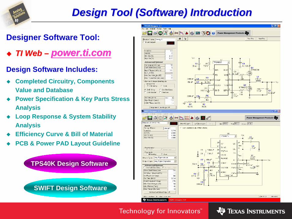
Design Tool (Software) IntroductionDesign Tool (Software) Introduction
Designer Software Tool:
TI Web TI Web –– power.ti.compower.ti.comDesign Software Includes:
Completed Circuitry, Components Value and DatabasePower Specification & Key Parts Stress AnalysisLoop Response & System Stability AnalysisEfficiency Curve & Bill of MaterialPCB & Power PAD Layout Guideline
SWIFT Design Software
TPS40K Design Software

33
Link to TI Power Website: Link to TI Power Website: power.ti.compower.ti.com
Quick SearchWeb: power.ti.com
Product Information
Selection Guides
New Products
Download Software

TI + Contract Manufacturer
Support
TI Field Applications
Engineers
TI Customer Service
Organization
TI Manufacturing
RepsTI
Distributors
CustomerCustomer
Factory Applications
TI Sales Engineers
Thanks for Your Time !
Website: power.ti.com
Related Documents