System Level SOC Design Unit 4a: Processors and Buses Overview • 7 course units over 5 days – Unit 1: Intro. to System Level Design – Unit 2: How to Define Requirements – Unit 3: Modeling for HW/SW Trade-offs – Unit 4: IP Selection • Processors and Buses – Unit 5: Embedded Software Codesign – Unit 6: Hardware Codesign/Coverification – Unit 7: Testing Outline • Topics – Types of processors and buses for SoC design – Picking a processor and a bus • Goal – Understanding of dominate processor organizations in SoC design – Issues on how to select a processor & bus The Design Process IDENTIFY requirements IDENTIFY requirements WRITE preliminary specs WRITE preliminary specs VERIFY/TEST HW models VERIFY/TEST HW models WRITE and DEVELOP SW prototype WRITE and DEVELOP SW prototype CO- SIMULATION CO- SIMULATION DEVELOP software DEVELOP software DETERMINE HW/SW partition DETERMINE HW/SW partition Library Canonical SoC Peripherals Peripherals Processor Processor I/O Interface I/O Interface Data Transformation Data Transformation Memory Memory I/O Interface I/O Interface Memory Controller Memory Controller Software Processors for SoC • SoC is centered around the processor – A critical component! – Select it carefully, and try to get it right upfront • Processor selection impacts SoC design – Processor performance for software IP – Power consumption of processor – Bus structure – Level of support (from vendor), tools, software development system

Welcome message from author
This document is posted to help you gain knowledge. Please leave a comment to let me know what you think about it! Share it to your friends and learn new things together.
Transcript
System Level SOC DesignUnit 4a: Processors and Buses Overview
• 7 course units over 5 days– Unit 1: Intro. to System Level Design – Unit 2: How to Define Requirements – Unit 3: Modeling for HW/SW Trade-offs – Unit 4: IP Selection
• Processors and Buses – Unit 5: Embedded Software Codesign– Unit 6: Hardware Codesign/Coverification– Unit 7: Testing
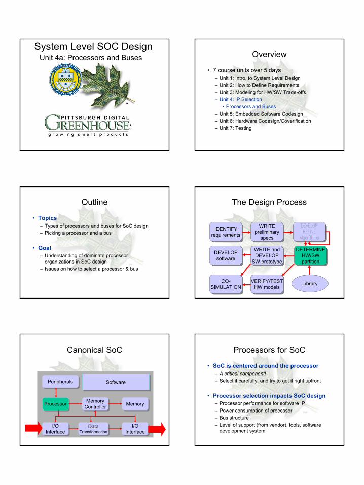
Outline
• Topics– Types of processors and buses for SoC design– Picking a processor and a bus
• Goal– Understanding of dominate processor
organizations in SoC design– Issues on how to select a processor & bus
The Design Process
IDENTIFYrequirementsIDENTIFY
requirementsWRITE
preliminaryspecs
WRITEpreliminary
specs
VERIFY/TESTHW models
VERIFY/TESTHW models
WRITE andDEVELOP
SW prototype
WRITE andDEVELOP
SW prototype
CO-SIMULATION
CO-SIMULATION
DEVELOPsoftware
DEVELOPsoftware
DETERMINEHW/SWpartition
DETERMINEHW/SWpartition
Library
Canonical SoC
PeripheralsPeripherals
ProcessorProcessor
I/OInterface
I/OInterface
DataTransformation
DataTransformation
MemoryMemory
I/OInterface
I/OInterface
MemoryControllerMemory
Controller
SoftwareSoftware
Processors for SoC
• SoC is centered around the processor– A critical component!– Select it carefully, and try to get it right upfront
• Processor selection impacts SoC design– Processor performance for software IP– Power consumption of processor– Bus structure– Level of support (from vendor), tools, software
development system
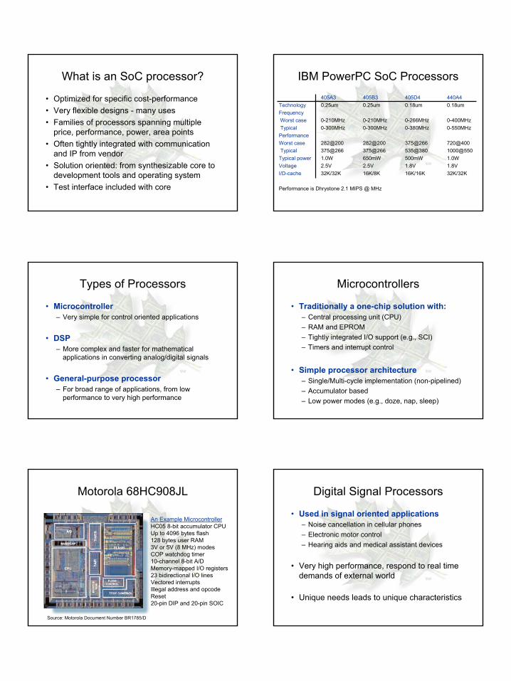
What is an SoC processor?
• Optimized for specific cost-performance• Very flexible designs - many uses• Families of processors spanning multiple
price, performance, power, area points• Often tightly integrated with communication
and IP from vendor• Solution oriented: from synthesizable core to
development tools and operating system• Test interface included with core
IBM PowerPC SoC Processors405A3 405B3 405D4 440A4
Technology 0.25um 0.25um 0.18um 0.18umFrequencyWorst case 0-210MHz 0-210MHz 0-266MHz 0-400MHzTypical 0-300MHz 0-300MHz 0-380MHz 0-550MHz
Performance Worst case 282@200 282@200 375@266 720@400Typical 375@266 375@266 535@380 1000@550
Typical power 1.0W 650mW 500mW 1.0WVoltage 2.5V 2.5V 1.8V 1.8VI/D-cache 32K/32K 16K/8K 16K/16K 32K/32K
Performance is Dhrystone 2.1 MIPS @ MHz
Types of Processors
• Microcontroller– Very simple for control oriented applications
• DSP– More complex and faster for mathematical
applications in converting analog/digital signals
• General-purpose processor– For broad range of applications, from low
performance to very high performance
Microcontrollers
• Traditionally a one-chip solution with:– Central processing unit (CPU)– RAM and EPROM – Tightly integrated I/O support (e.g., SCI)– Timers and interrupt control
• Simple processor architecture– Single/Multi-cycle implementation (non-pipelined)– Accumulator based– Low power modes (e.g., doze, nap, sleep)
Motorola 68HC908JL
An Example MicrocontrollerHC05 8-bit accumulator CPUUp to 4096 bytes flash128 bytes user RAM3V or 5V (8 MHz) modesCOP watchdog timer10-channel 8-bit A/DMemory-mapped I/O registers23 bidirectional I/O linesVectored interruptsIllegal address and opcodeReset20-pin DIP and 20-pin SOIC
Source: Motorola Document Number BR1785/D
Digital Signal Processors
• Used in signal oriented applications– Noise cancellation in cellular phones– Electronic motor control– Hearing aids and medical assistant devices
• Very high performance, respond to real time demands of external world
• Unique needs leads to unique characteristics
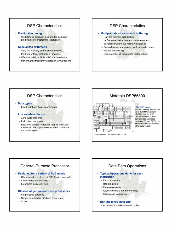
DSP Characteristics
• Predictable timing– Well defined behavior, designed to be highly
predictable by programmer (statically)
• Specialized arithmetic– Very fast multiply-and-accumulate (MAC)– Plethora of MAC instruction variations– Often includes multiple MAC functional units– Performance frequently quoted in MACs/second
DSP Characteristics
• Multiple data streams with buffering– Harvard memory architecture
• Separate instruction and data memories– Several simultaneous memory accesses– Banked memories, possibly with separate buses– Modulo addressing– Large number of registers to buffer values
DSP Characteristics
• Data types– Fixed-point and floating-point data
• Low overhead loops– Zero-cycle branches– Instruction memories– E.g., loop caches - captures loop in small, fast
memory close to processor where it can run at maximum speed
Motorola DSP56800
16-bit DSP engineHarvard memory architectureUp to 40M MACs/second16x16 bit parallel MACTwo 36-bit accumulatorsDSP addressing modesHardware DO and REP loopsBit manipulation instructionsMCU features (I/O)
Source: Motorola Document Number AA1445
General-Purpose Processor
• Designed for a variety of SoC needs– Often includes features of DSP & microcontroller– Clock rate is easily scaled– Extensible instruction sets
• Classes of general-purpose processors– Single-issue pipelined– Simple superscalar pipelined (dual issue)– VLIW
Data Path Operations
• Typical operations done for each instruction– Fetch instruction– Read registers– Execute operation– Access memory and do branches– Write result to registers
• Non-pipelined data path– An instruction takes several cycles
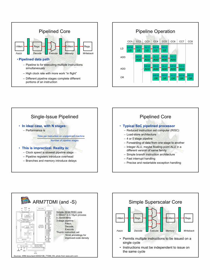
Pipelined Core
Pipelined data path– Pipeline to for executing multiple instructions
simultaneously
– High clock rate with more work “in flight”
– Different pipeline stages complete different portions of an instruction
Fetch Decode Execute Memory Writeback
I-Mem Regs. Regs.D-Mem
•
Pipeline Operation
CC1 CC2 CC3 CC4 CC5 CC6 CC7 CC8
MEMLD
REGLD
ALULD
MEMLD
REGLD
MEMADD
REGADD
ALUADD
MEMADD
REGADD
MEMADD
REGADD
ALUADD
MEMADD
REGADD
MEMOR
REGOR
ALUOR
MEMOR
REGOR
LD
ADD
ADD
OR
Single-Issue Pipelined
• In ideal case, with N stages:– Performance is
• This is impractical. Reality is:– Clock speed is slowest pipeline stage– Pipeline registers introduce overhead– Branches and memory introduce delays
Time per instruction on unpipelined machine
Number of pipeline stages
Pipelined Core
• Typical SoC pipelined processor– Reduced instruction set computer (RISC)– Load-store architecture– 4 or 5 stage pipeline– Forwarding of data from one stage to another– Integer ALU, maybe floating-point ALU in a
different version of same family– Simple branch instruction architecture– Fast interrupt handling– Precise and restartable exception handling
ARM7TDMI (and -S)
Simple 32-bit RISC core0.59mm2 in 0.18µm process0.25mW/MHz3 stage pipeline:
Fetch,Decode,Execute
Thumb instruction set16-bit encodings forimproved code density
Sources: ARM document DDI0210B_7TDMI_R4, photo from www.arm.com
Simple Superscalar Core
• Permits multiple instructions to be issued on a single cycle
• Instructions must be independent to issue on the same cycle
Fetch Decode Execute Memory Writeback
I-Mem Regs. Regs.D-Mem
Simple Superscalar Core
• For SoC processors– Typically at most dual-issue core– Usually in-order issue, possibly out-of-order
execution– Usually statically scheduled (by the compiler) to
take advantage of dual-issue capability– Dynamic scheduling is possible
• Simple cores for low cost (area, power), predictability, and flexibility
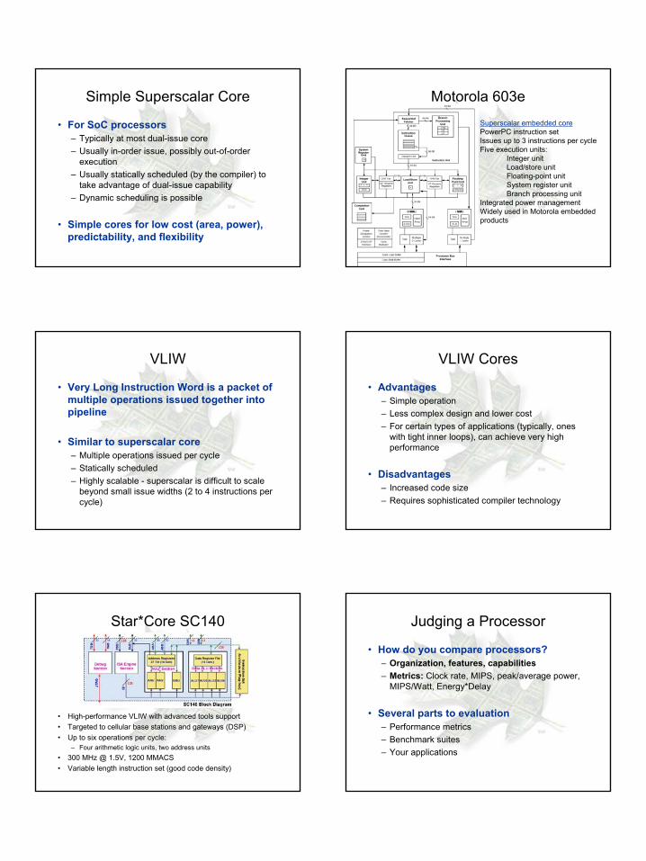
Motorola 603e Superscalar embedded corePowerPC instruction setIssues up to 3 instructions per cycleFive execution units:
Integer unitLoad/store unitFloating-point unitSystem register unitBranch processing unit
Integrated power managementWidely used in Motorola embeddedproducts
VLIW
• Very Long Instruction Word is a packet of multiple operations issued together into pipeline
• Similar to superscalar core– Multiple operations issued per cycle– Statically scheduled– Highly scalable - superscalar is difficult to scale
beyond small issue widths (2 to 4 instructions per cycle)
VLIW Cores
• Advantages– Simple operation– Less complex design and lower cost– For certain types of applications (typically, ones
with tight inner loops), can achieve very high performance
• Disadvantages– Increased code size– Requires sophisticated compiler technology
Star*Core SC140
• High-performance VLIW with advanced tools support• Targeted to cellular base stations and gateways (DSP)• Up to six operations per cycle:
– Four arithmetic logic units, two address units• 300 MHz @ 1.5V, 1200 MMACS• Variable length instruction set (good code density)
Judging a Processor
• How do you compare processors?– Organization, features, capabilities– Metrics: Clock rate, MIPS, peak/average power,
MIPS/Watt, Energy*Delay
• Several parts to evaluation– Performance metrics– Benchmark suites– Your applications
Clock Rate
• How fast the processor is clocked?• An indication of performance potential
• Actual performance not dictated purely by clock rate– Execution time = IC * CPI * Clock rate– CPI is highly dependent on organization
• For a fixed organization, clock rate is a useful metric
MIPS
• Million Instructions Per Second• Attempts to factor out
– Clock rate– Organization
• But.... MIPS may not indicate actual performance– Often quoted as the peak performance– Highly dependent on instruction mix and what is
being done
Dhrystone 2.1
• Common basis for comparison (what’s being measured is known, unlike MIPS)
• Synthetic benchmark program (1-1.5KB) that is supposed to be representative of system programming (integer code)
• Based on statistical analysis of use of programming language features
• Very popular in embedded community
Dhrystone 2.1
• But.... is it representative of your code?– Very small size, so memory system not tested– Easily optimized by compiler– String operations very prevelant– Fixed-point? Floating-point?
• Better than clock rate or peak MIPS for a quick evaluation of performance but don’t blindly rely on it (or trust vendor numbers)
Benchmark Suite
• Selection of representative applications• Embedded Microprocessor Benchmark
Consortium (EEMBC)– Automotive/industrial, consumer, networking,
office automation, and telecommunications markets. Engine control, digital cameras, printers, cellular phones, modems, etc.
• Membership required, entitling you to access to benchmark code and results for numerous processor cores
Code Size
• Static code size measures instruction memory requirements
• Dependent on– Application (complexity)– Instruction set architecture
• Encoding of instruction (fixed vs. variable)• Encoding of addressing modes• Compressed instruction sets

Power Consumption
• How much power the processor consumes
• Often qouted as:– Peak vs. average power– Power at a given frequency, voltage
• Processor dynamic power: Pd = αfCV2
• Other metrics: MIPS/Watt, Energy*Delay
Energy X Delay
00.20.40.60.8
11.2
Unp
ipel
ined
Pipe
lined
Supe
rsca
lar
Nor
malized
Ene
rgy
00.5
11.5
22.5
33.5
4
Unp
ipel
ined
Pipe
lined
Supe
rsca
larNor
malized
Per
form
ance
Energy X Delay
• Unpipelined best energy but poor energy X delay
• Going from Pipelined to Superscalar doesn’t help much
00.5
11.5
22.5
3
Unp
ipel
ined
Pipe
lined
Supe
rsca
lar
Ener
gy X
Delay
Your Code
• Ultimate evaluation– Based on your application– Based on execution time and meeting
performance needs of your application– Actual metrics: execution time, power, code size
• Always remember– Benchmark numbers for broad-basis comparison
and initial selection (a guess)– Then evaluate on your code!
Selecting a Processor
• Based on performance, cost, power consumption
• Familiarity with the core family (and tools)• Tools, operating system, support,
documentation availability and cost• Licensing and royalities• Multiple party sourced• Bus structure and performance
Documentation
• Is documentation available for the selected processor core?– Vital to successfully developing with a chosen
core– Best case: all documents on the web– Worst case: you have to talk to one person
• Example: ARM documents– visit www.arm.com, all documents in PDF online– Except: some closely-held documents (e.g., buses
for ARM)
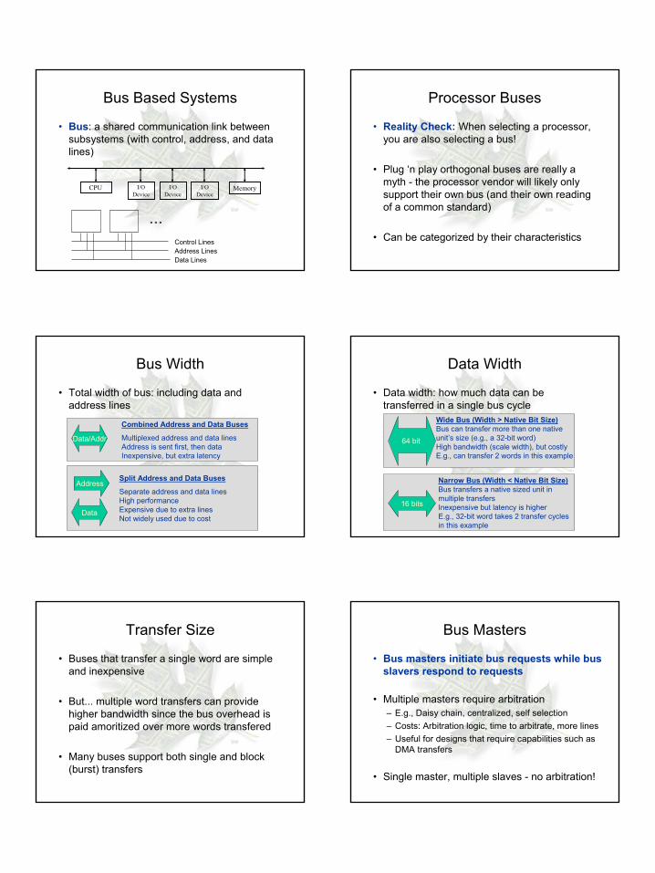
Bus Based Systems
• Bus: a shared communication link between subsystems (with control, address, and data lines)
I/O Device
I/O Device
I/O Device
CPU Memory
° ° °
Control LinesAddress LinesData Lines
Processor Buses
• Reality Check: When selecting a processor, you are also selecting a bus!
• Plug ‘n play orthogonal buses are really a myth - the processor vendor will likely only support their own bus (and their own reading of a common standard)
• Can be categorized by their characteristics
Bus Width
• Total width of bus: including data and address lines
Data/Addr
Data
AddressSeparate address and data linesHigh performanceExpensive due to extra linesNot widely used due to cost
Split Address and Data Buses
Multiplexed address and data linesAddress is sent first, then dataInexpensive, but extra latency
Combined Address and Data Buses
Data Width
• Data width: how much data can be transferred in a single bus cycle
64 bit
16 bits
Wide Bus (Width > Native Bit Size)Bus can transfer more than one nativeunit’s size (e.g., a 32-bit word)High bandwidth (scale width), but costlyE.g., can transfer 2 words in this example
Narrow Bus (Width < Native Bit Size)Bus transfers a native sized unit in multiple transfersInexpensive but latency is higher E.g., 32-bit word takes 2 transfer cyclesin this example
Transfer Size
• Buses that transfer a single word are simple and inexpensive
• But... multiple word transfers can provide higher bandwidth since the bus overhead is paid amoritized over more words transfered
• Many buses support both single and block (burst) transfers
Bus Masters
• Bus masters initiate bus requests while bus slavers respond to requests
• Multiple masters require arbitration– E.g., Daisy chain, centralized, self selection– Costs: Arbitration logic, time to arbitrate, more lines– Useful for designs that require capabilities such as
DMA transfers
• Single master, multiple slaves - no arbitration!
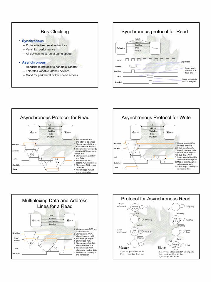
Bus Clocking
• Synchronous– Protocol is fixed relative to clock– Very high performance– All devices must run at same speed!
• Asynchronous– Handshake protocol to handle a transfer– Tolerates variable latency devices– Good for peripheral or low speed access
Synchronous protocol for Read
Master Slave
clock
addressReadReqData
DataRdy
clock
address
ReadReq
Data
DataRdy
Begin read
Slave readsthe data in afixed time
Slave writes dataon a fixed cycle
Asynchronous Protocol for Read
13
4
57
6
2 2
address
6
Master SlaveaddressReadReqData
DataRdy
Ack
ReadReq
Ack
DataRdy
Data
4
1: Master asserts REQ and addr. to do a read
2: Slave asserts ACK whenit has read the address
3: Master acknowledges bydropping REQ and slavedrops ACK
4: Slave asserts DataRdy and Data
5: Master reads data, asserts ACK when done
6: Slave sees ACK, dropsdata lines
7: Master drops ACK atend of transaction
Asynchronous Protocol for Write
13
4
57
6
2 2
2
Master SlaveaddressWriteReqDataDataRdy
Ack
address
WriteReq
Data
DataRdy
Ack
1: Master asserts REQ,address and data
2: Slave asserts ACK, when it has read data
3: Master drops request4: Slave drops ACK5: Slave asserts DataRdy
when done writing data6: Master asserts ACK to
acknowledge write7: Slave drops DataRdy to
end transaction
Multiplexing Data and Address Lines for a Read
13
4
57
6
2 2
Master Slave
AckReadReq
Data/addressDataRdy
46
Ack
ReadReq
Data/address
DataRdy
1: Master asserts REQ andaddress on bus
2: Slave asserts ACK, when it has read addr.
3: Master drops request4: Slave drops ACK5: Slave asserts DataRdy
when data is on bus6: Master asserts ACK
when done reading data7: Slave drops DataRdy to
end transaction
Protocol for Asynchronous Read
A_out == put address on busD_in == read data from bus
A newread request
Ack& D_in
ReadReq& A_out
DataRdy
Ack
DataRdy
DataRdy
A newread request
DataRdy
Ack
Ack& A_in
Done
ReqdReq
Done
ReadReq
ReadReq
ReqdReq
DataRdy& D_out
Ack
Ack
MasterA_in == read address and start fetching dataDone == finished fetching dataD_out == put data on bus
Slave
Protocol for Asynchronous Read (The Master)
NR
Ack
DR
Logic for implementingthe finite state
machine
RR Ack A_outD_in
State register (2 bits)
Next State
NR
Ack& D_in
RR& A_out
Ack
DR
DR
Ack
NR
DR
DRData Address
The bus
2
200
01
10
11NR = new requestRR = ReadReqDR = DataRdy
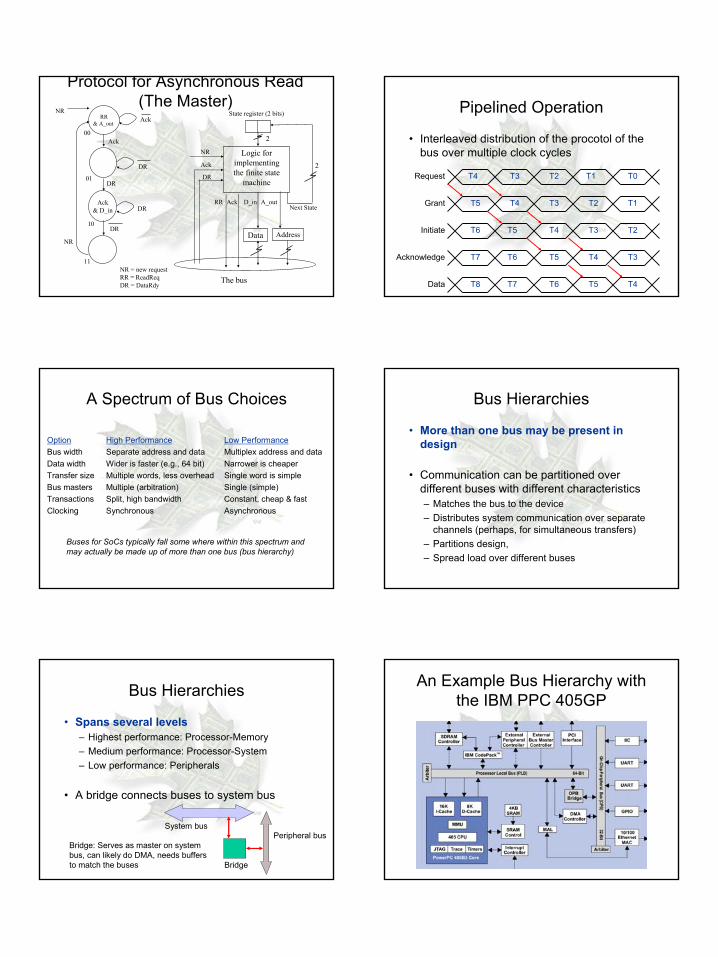
Pipelined Operation
• Interleaved distribution of the procotol of the bus over multiple clock cycles
Request
Grant
Initiate
Acknowledge
Data
T4
T4
T4
T4
T4
T0T1T2T3
T3
T3
T3
T2
T2
T1T5
T5
T5
T5
T6
T6
T6
T7
T7T8
A Spectrum of Bus Choices
Option High Performance Low PerformanceBus width Separate address and data Multiplex address and dataData width Wider is faster (e.g., 64 bit) Narrower is cheaperTransfer size Multiple words, less overhead Single word is simpleBus masters Multiple (arbitration) Single (simple)Transactions Split, high bandwidth Constant, cheap & fastClocking Synchronous Asynchronous
Buses for SoCs typically fall some where within this spectrum andmay actually be made up of more than one bus (bus hierarchy)
Bus Hierarchies
• More than one bus may be present in design
• Communication can be partitioned over different buses with different characteristics– Matches the bus to the device– Distributes system communication over separate
channels (perhaps, for simultaneous transfers)– Partitions design, – Spread load over different buses
Bus Hierarchies
• Spans several levels– Highest performance: Processor-Memory– Medium performance: Processor-System– Low performance: Peripherals
• A bridge connects buses to system bus
System busPeripheral bus
Bridge
Bridge: Serves as master on systembus, can likely do DMA, needs buffersto match the buses
An Example Bus Hierarchy with the IBM PPC 405GP
Selecting a Bus
• Performance metrics– Latency: Time to execute a transaction on bus
Access latency Transfer time
Dependent on bus protocol, includingthe need for bus arbitration
Determined by the bus protocol, bus width, andthe packet size of data sent over the bus (block size)
Selecting a Bus
• Performance metrics– Bandwidth: Maximum capacity of transfer as a
function of time (amount of data per unit time)
Synchronous memory busBus width 64 bits, 100 MHzPeak bandwidth is the
absolute maximum transfer rate.
Bandwidth can be limited by the access latency.
Example: Reading a memory location1. Send address (10 ns),2. Memory access (100 ns),3. Receive data (10 ns)4. One cycle turn-around (10 ns)Total latency = 10+100+10+10 = 130 nsBandwidth = 8 bytes / 130 ns =
Guidelines for Selecting a Bus
• Processor-memory (may be done over system bus)• Single connection: processor to memory, high-
speed, synchronous, often 64-256 bits wide, single bus master
• System• High to medium speed based on total needs of all
system blocks, synchronous or asynchronous, often 32-64 bits wide, multiple masters
• Peripherals• Low speed, asynchronous, narrow width of 8-32
bits, single master
An Example
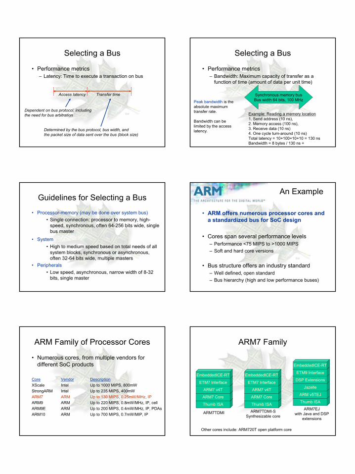
• ARM offers numerous processor cores and a standardized bus for SoC design
• Cores span several performance levels– Performance <75 MIPS to >1000 MIPS– Soft and hard core versions
• Bus structure offers an industry standard– Well defined, open standard– Bus hierarchy (high and low performance buses)
ARM Family of Processor Cores
• Numerous cores, from multiple vendors for different SoC products
Core Vendor DescriptionXScale Intel Up to 1000 MIPS, 800mWStrongARM Intel Up to 235 MIPS, 400mWARM7 ARM Up to 130 MIPS, 0.25mW/MHz, IPARM9 ARM Up to 220 MIPS, 0.8mW/MHz, IP, cellARM9E ARM Up to 200 MIPS, 0.4mW/MHz, IP, PDAsARM10 ARM Up to 700 MIPS, 0.7mW/MIP, IP
ARM7 Family
Thumb ISA
ARM7 Core
ARM7 v4T
ETM7 Interface
EmbeddedICE-RT
Thumb ISA
ARM7 Core
ARM7 v4T
ETM7 Interface
EmbeddedICE-RT
Thumb ISA
ARM v5TEJ
Jazelle
DSP Extensions
ARM7TDMI ARM7TDMI-SSynthesizable core
ARM7EJwith Java and DSP
extensions
ETM9 Interface
EmbeddedICE-RT
Other cores include: ARM720T open platform core
ARM7 Features
• Established, high-volume architecture • OS and RTOS support - including Windows
CE, Palm OS, Symbian OS, and Linux• ARM development tools and simulation
models for major EDA environments • Built-in debug support• Multiple sourcing with availability in 0.25µm,
0.18µm and 0.13µm processes
ARM Thumb ISA
• Compressed instruction set– 16-bit vs. 32-bit instructions– Only most common opcodes– Fewer register specifiers
• Decompressed in core
• Reduces memory footprint• Improves bandwidth utilization to memory
Tour of ARM Developer’s Suite
Developer’s suite includes:– Efficient optimizing C++ compiler– Integrated development environment
• CodeWarrior IDE from Metrowerks• Graphical user interface with source and
project management– Math libraries with known worst case performance– Assembler and linker with multilple formats– Debugger and simulator (ARMulator)– Price $6500 for one floating license
Picture source: ARM web site: www.arm.com
ARM AMBA Bus
Picture source: www.arm.com
Open bus specification for SoC designs from ARM
Two bus architectures: Advanced High Performance Bus (AHB)Advanced Peripheral Bus (APB)
Components include: design kit, compliance test bench, andcompliance certification program
Typical AMBA Bus Design AMBA AHB
• High performance, high bandwidth– Connection to processor and high bandwidth
devices– Bridge to connect with peripheral devices on APB
• Characteristics– Synchronous – Width of 32 to 1024 bits– Multiple bus masters– Split transactions– Pipelined and burst transfers
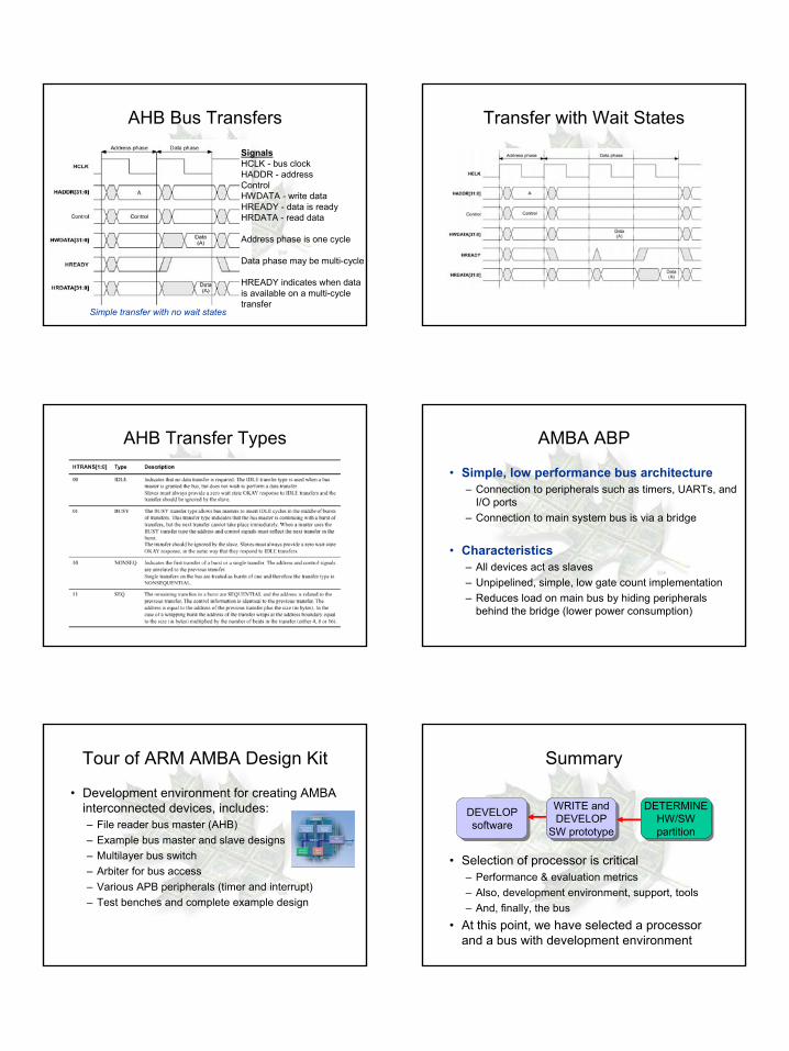
AHB Bus Transfers
Simple transfer with no wait states
SignalsHCLK - bus clockHADDR - addressControlHWDATA - write dataHREADY - data is readyHRDATA - read data
Address phase is one cycle
Data phase may be multi-cycle
HREADY indicates when datais available on a multi-cycletransfer
Transfer with Wait States
AHB Transfer Types AMBA ABP
• Simple, low performance bus architecture– Connection to peripherals such as timers, UARTs, and
I/O ports– Connection to main system bus is via a bridge
• Characteristics– All devices act as slaves– Unpipelined, simple, low gate count implementation– Reduces load on main bus by hiding peripherals
behind the bridge (lower power consumption)
Tour of ARM AMBA Design Kit
• Development environment for creating AMBA interconnected devices, includes:– File reader bus master (AHB)– Example bus master and slave designs– Multilayer bus switch– Arbiter for bus access– Various APB peripherals (timer and interrupt)– Test benches and complete example design
Summary
• Selection of processor is critical– Performance & evaluation metrics– Also, development environment, support, tools– And, finally, the bus
• At this point, we have selected a processor and a bus with development environment
WRITE andDEVELOP
SW prototype
WRITE andDEVELOP
SW prototypeDEVELOPsoftware
DEVELOPsoftware
DETERMINEHW/SWpartition
DETERMINEHW/SWpartition
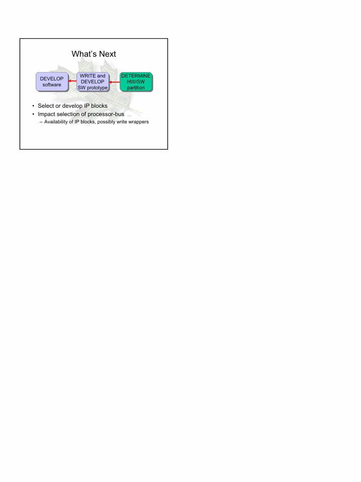
What’s Next
• Select or develop IP blocks• Impact selection of processor-bus
– Availability of IP blocks, possibly write wrappers
WRITE andDEVELOP
SW prototype
WRITE andDEVELOP
SW prototypeDEVELOPsoftware
DEVELOPsoftware
DETERMINEHW/SWpartition
DETERMINEHW/SWpartition
Related Documents