System Design: Peripheral ICs and Interfacing Chapter 7

Welcome message from author
This document is posted to help you gain knowledge. Please leave a comment to let me know what you think about it! Share it to your friends and learn new things together.
Transcript
System Design: Peripheral
ICs and Interfacing
Chapter 7
2011 Microcontrollers-... 2nd Ed. Raj Kamal
Pearson Education2
Lesson 5
ADC - Analog to Digital Converter
2011 Microcontrollers-... 2nd Ed. Raj Kamal
Pearson Education3
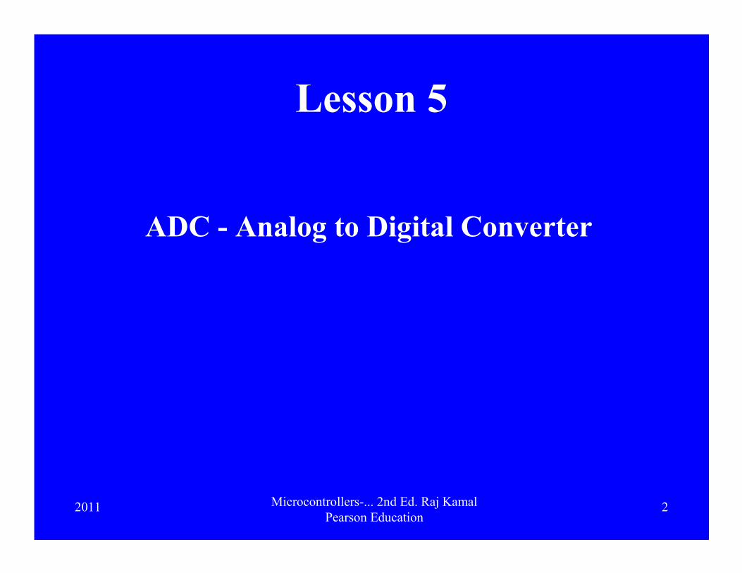
Analog to Digital Conversion (ADC)
� Need of Analog signal to be converted into bits in many applications
� Need a reference input (Vref+) = The maximum input when after conversion output bits= all 1s)
� Need Vref− = The minimum input when after conversion output bits= all 0s)
� Generates Digital output bits proportional to the ADC analog input
2011 Microcontrollers-... 2nd Ed. Raj Kamal
Pearson Education4
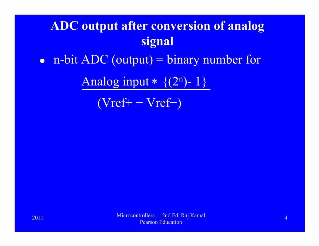
ADC output after conversion of analog
signal
� n-bit ADC (output) = binary number for
Analog input ∗ {(2n)- 1}
(Vref+ − Vref−)

2011 Microcontrollers-... 2nd Ed. Raj Kamal
Pearson Education5
8-bit ADC example
� Assume that 8-bit ADC Vref+ = 1.275 V and Vref− = 0 V.
� Output bits = all 0s = 00000000 (=0d) when input = 0V,
� Output bits = 10000000 (= 128d) when input = 0.64V and
� Output bits = 11111111 (= 255d) when input = 1.275V
2011 Microcontrollers-... 2nd Ed. Raj Kamal
Pearson Education6
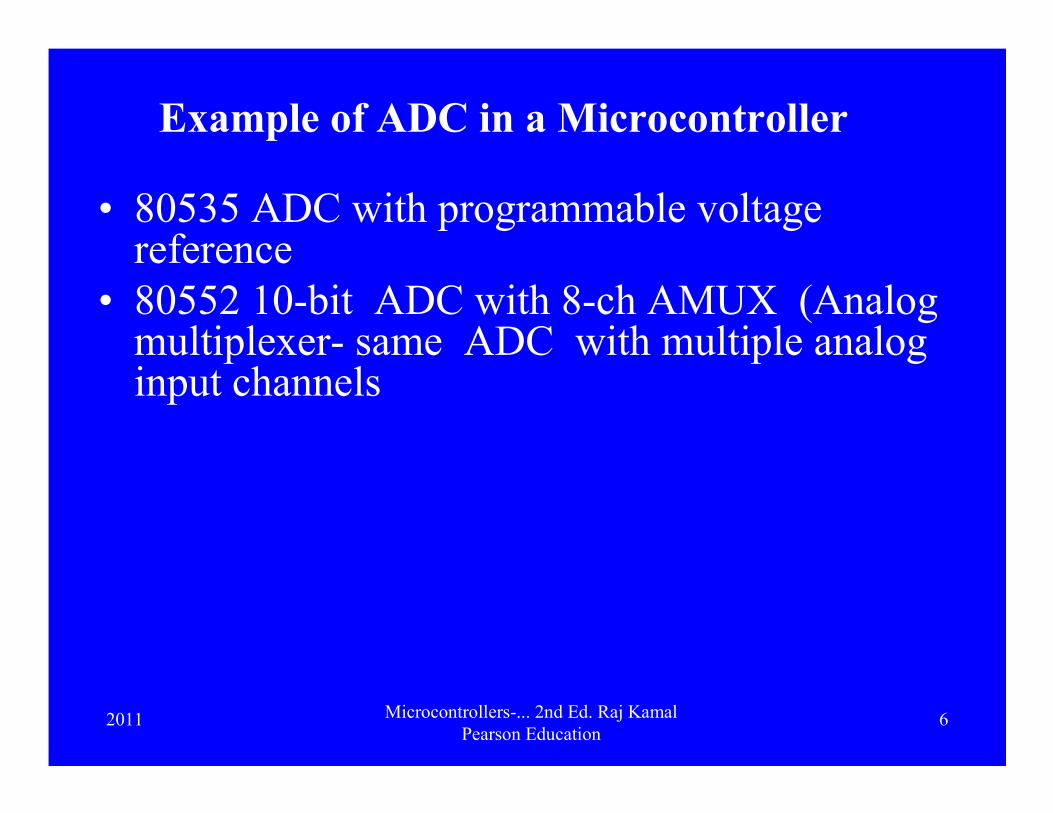
Example of ADC in a Microcontroller
• 80535 ADC with programmable voltage reference
• 80552 10-bit ADC with 8-ch AMUX (Analog multiplexer- same ADC with multiple analog input channels

2011 Microcontrollers-... 2nd Ed. Raj Kamal
Pearson Education7
ADC Chips for interfacing
processors buses and MCUs ports
• ADC04 one channel ADC with voltage
reference = 1/2 of maximum permitted analog
input
• ADC0808 eight channels ADC with voltage
reference + and -inputs
• ADC0816 sixteen channels
Example of ADC in a Microcontroller
2011 Microcontrollers-... 2nd Ed. Raj Kamal
Pearson Education8
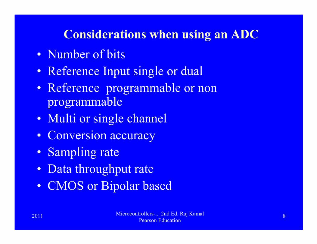
Considerations when using an ADC
• Number of bits
• Reference Input single or dual
• Reference programmable or non programmable
• Multi or single channel
• Conversion accuracy
• Sampling rate
• Data throughput rate
• CMOS or Bipolar based
2011 Microcontrollers-... 2nd Ed. Raj Kamal
Pearson Education9
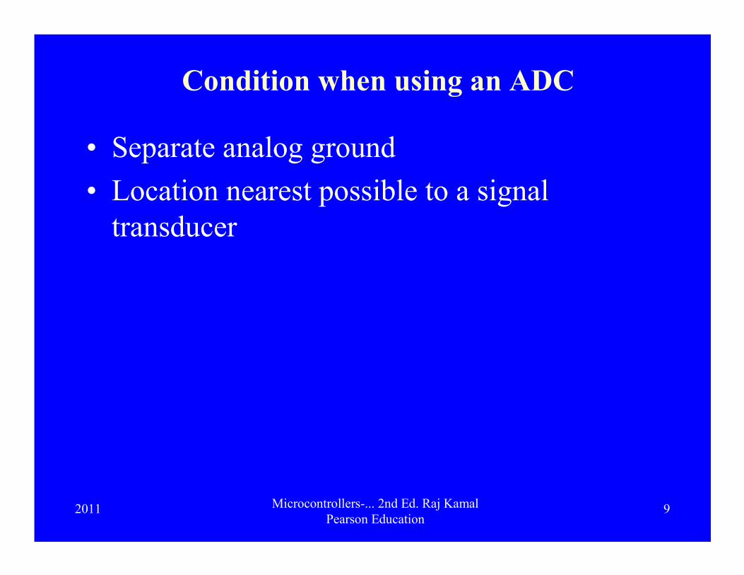
Condition when using an ADC
• Separate analog ground
• Location nearest possible to a signal
transducer

2011 Microcontrollers-... 2nd Ed. Raj Kamal
Pearson Education10
• 8 bit ADC
• Interfaces with microcontroller ports or processor data and control bus signals
D0-D7, RD and WR and INTR
• Requires Vref/2 input
• Converted output = 1000 000b output when analog input = Vref/2
• WR input results in start of conversion (SOC)
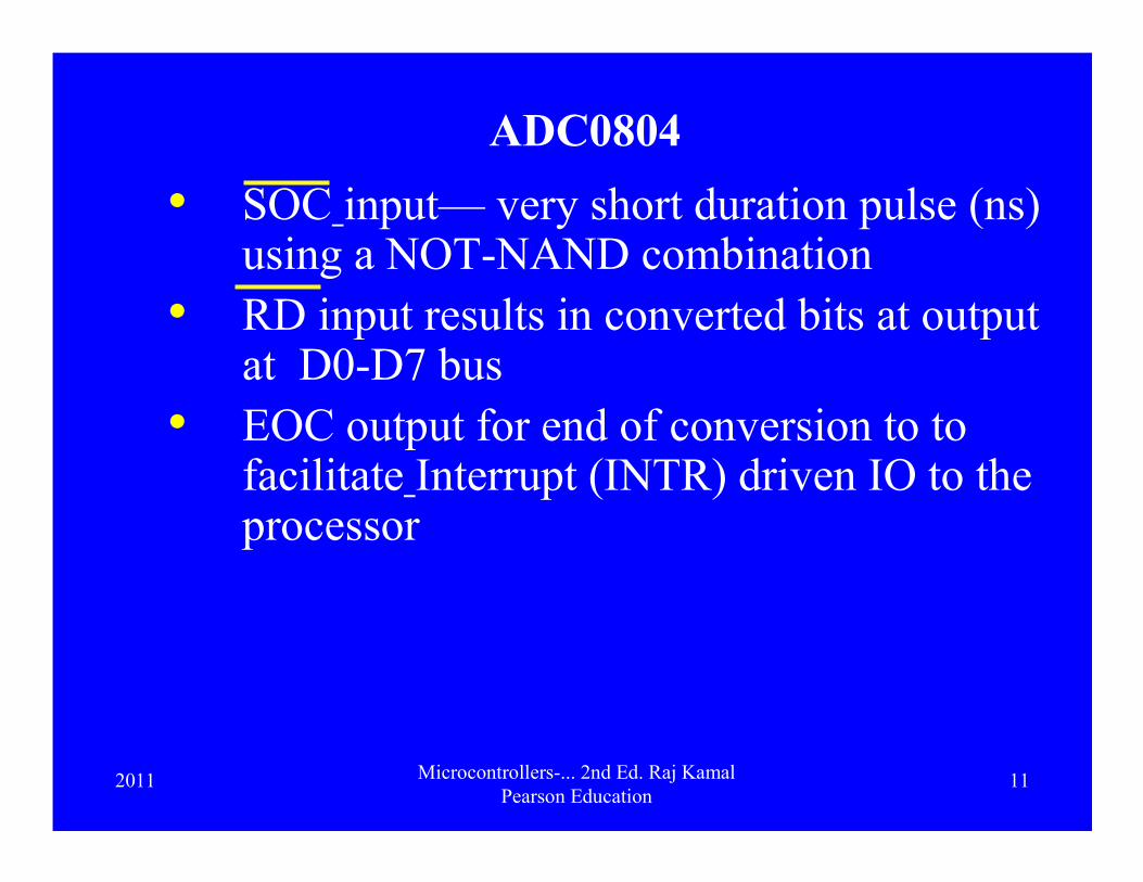
ADC0804
2011 Microcontrollers-... 2nd Ed. Raj Kamal
Pearson Education11
• SOC input— very short duration pulse (ns) using a NOT-NAND combination
• RD input results in converted bits at output at D0-D7 bus
• EOC output for end of conversion to tofacilitate Interrupt (INTR) driven IO to the processor
ADC0804

2011 Microcontrollers-... 2nd Ed. Raj Kamal
Pearson Education12
• Separate analog and digital grounds to
isolate digital transitions noise by direct
connection of ANALOG-GND to supply
GND
• Clock frequency adjustable by external RC
pair timing constant
ADC0804
2011 Microcontrollers-... 2nd Ed. Raj Kamal
Pearson Education13
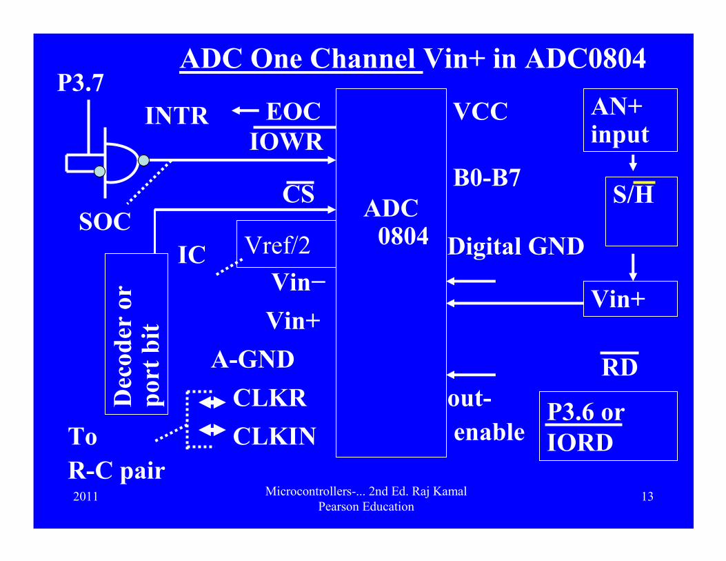
VCCEOC
CS
Vin−
S/H
Digital GND
RD
B0-B7
IOWR
Vref/2
A-GND
CLKIN
CLKR
Vin+
INTR
P3.7
SOC
Dec
od
er o
r p
ort
bit
To
R-C pair
P3.6 or
IORD
IC
AN+ input
Vin+
out-
enable
ADC One Channel Vin+ in ADC0804
ADC 0804
2011 Microcontrollers-... 2nd Ed. Raj Kamal
Pearson Education14
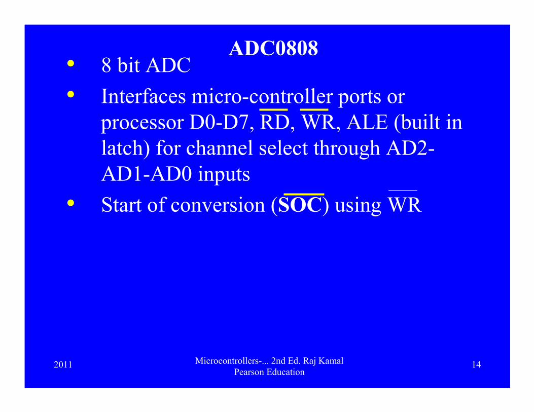
• 8 bit ADC
• Interfaces micro-controller ports or
processor D0-D7, RD, WR, ALE (built in
latch) for channel select through AD2-
AD1-AD0 inputs
• Start of conversion (SOC) using WR
ADC0808

2011 Microcontrollers-... 2nd Ed. Raj Kamal
Pearson Education15
• SOC input very short duration (ns) pulse using a NOT-NAND combination
• output enable for converted bits on D0-D7 using RD
• EOC output for end of conversion to facilitate interrupt (INTR) driven IO
ADC0808

2011 Microcontrollers-... 2nd Ed. Raj Kamal
Pearson Education16
• Separate analog and digital grounds to
separate digital transitions noise by direct
connection of A-GND to supply GND
• Clock frequency input
ADC0808
2011 Microcontrollers-... 2nd Ed. Raj Kamal
Pearson Education17
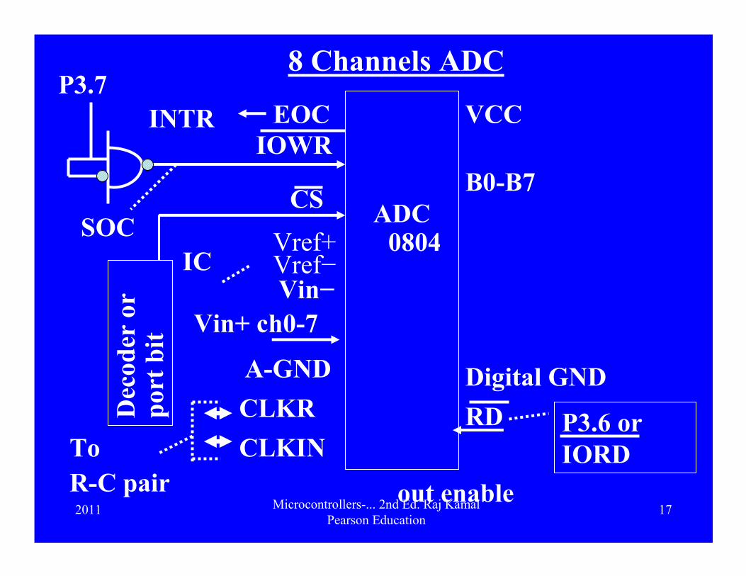
VCCEOC
CS
Vin−
Digital GND
RD
B0-B7
IOWR
Vref+
A-GND
CLKIN
CLKR
Vin+ ch0-7
INTR
P3.7
SOC
Dec
od
er o
r p
ort
bit
To
R-C pair
P3.6 or
IORD
IC
out enable
8 Channels ADC
ADC 0804
Vref−

2011 Microcontrollers-... 2nd Ed. Raj Kamal
Pearson Education18
B0-B7 connects to data AD0-AD7
out-enable
IORD
CS
RDS/H
Ch0 AN+ input
ch0 Vin+
Interfacing ADC0808

2011 Microcontrollers-... 2nd Ed. Raj Kamal
Pearson Education19
• 8 bit ADC
• Interfaces micro-controller ports or processor data buses (D0-D7), RD, WR, ALE for channel select through AD3-AD2-AD1-AD0 bus inputs (also separate A3-A0),
• WR input for start of conversion (SOC)
ADC0816

2011 Microcontrollers-... 2nd Ed. Raj Kamal
Pearson Education20
• Separate output enable input for expanding the number of channels
• Analog multiplexer in-built gives the analog output for the filter and S/H inputs and then hold outputs to get analog inputs for conversion (External S/H and filter not needed for channels)
ADC0816
2011 Microcontrollers-... 2nd Ed. Raj Kamal
Pearson Education21
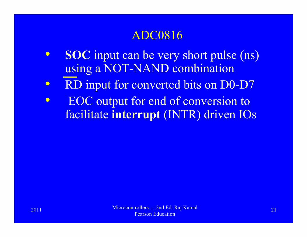
• SOC input can be very short pulse (ns) using a NOT-NAND combination
• RD input for converted bits on D0-D7
• EOC output for end of conversion to facilitate interrupt (INTR) driven IOs
ADC0816

2011 Microcontrollers-... 2nd Ed. Raj Kamal
Pearson Education22
• Separate analog and digital grounds to
separate digital transitions noise by direct
connection of A-GND to supply GND
• Clock frequency input
ADC0816
2011 Microcontrollers-... 2nd Ed. Raj Kamal
Pearson Education23
ADC 0808
VCCEOC
AMUX output
Vref-Digital GND
RD
B0-B7
IOWR
Vref+
A-GND
CLKIN
CLKR
Vin+Ch0-15
INTR
Vout
RC pair
P3.6 or
IORDIC
ALE IN
out enable
ADC 16- Channels
ChA0-ChA3
P3.7
expansion
control
2011 Microcontrollers-... 2nd Ed. Raj Kamal
Pearson Education24
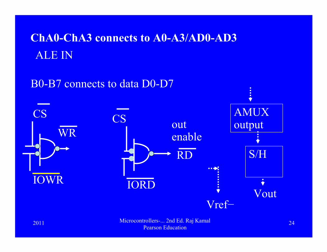
B0-B7 connects to data D0-D7
ChA0-ChA3 connects to A0-A3/AD0-AD3
CSout enable
ALE IN
IOWR IORD
CS
RD S/H
AMUX output
VoutVref−
WR
2011 Microcontrollers-... 2nd Ed. Raj Kamal
Pearson Education25
Table 7.20 - Each Pin signals
Table 7.19 - Functions of
subunits in circuit
2011 Microcontrollers-... 2nd Ed. Raj Kamal
Pearson Education26
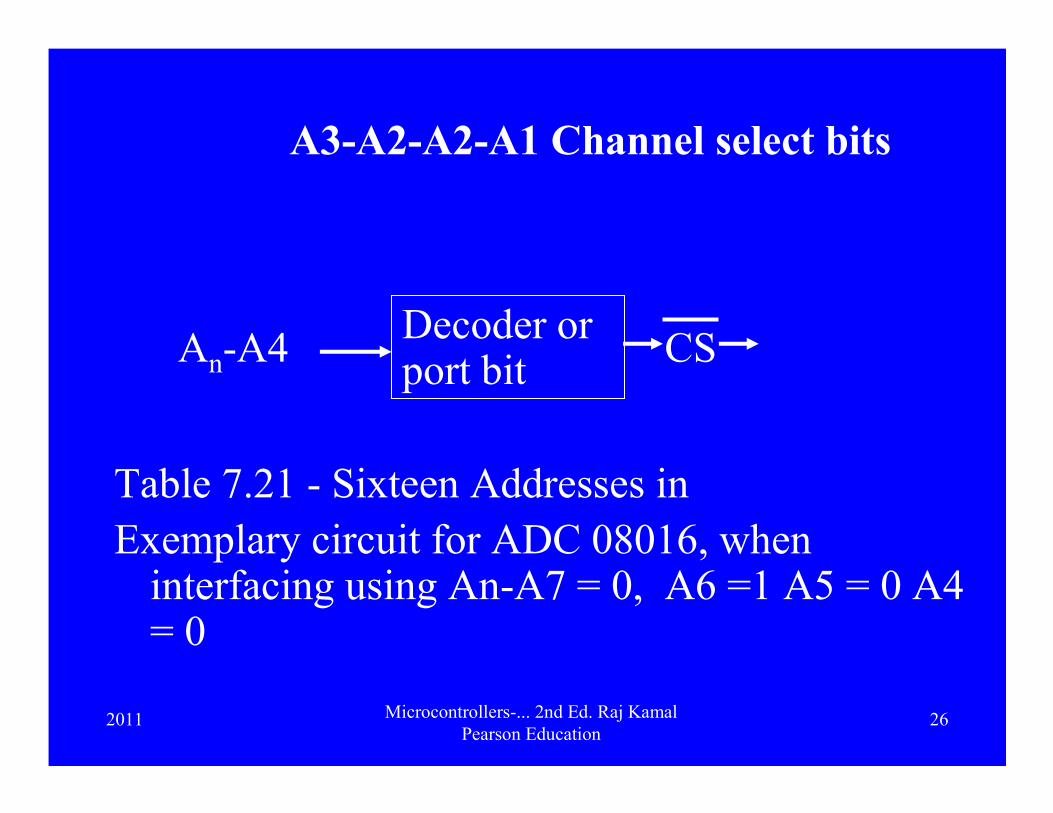
Table 7.21 - Sixteen Addresses in
Exemplary circuit for ADC 08016, when interfacing using An-A7 = 0, A6 =1 A5 = 0 A4 = 0
A3-A2-A2-A1 Channel select bits
CSAn-A4Decoder or port bit
2011 Microcontrollers-... 2nd Ed. Raj Kamal
Pearson Education27
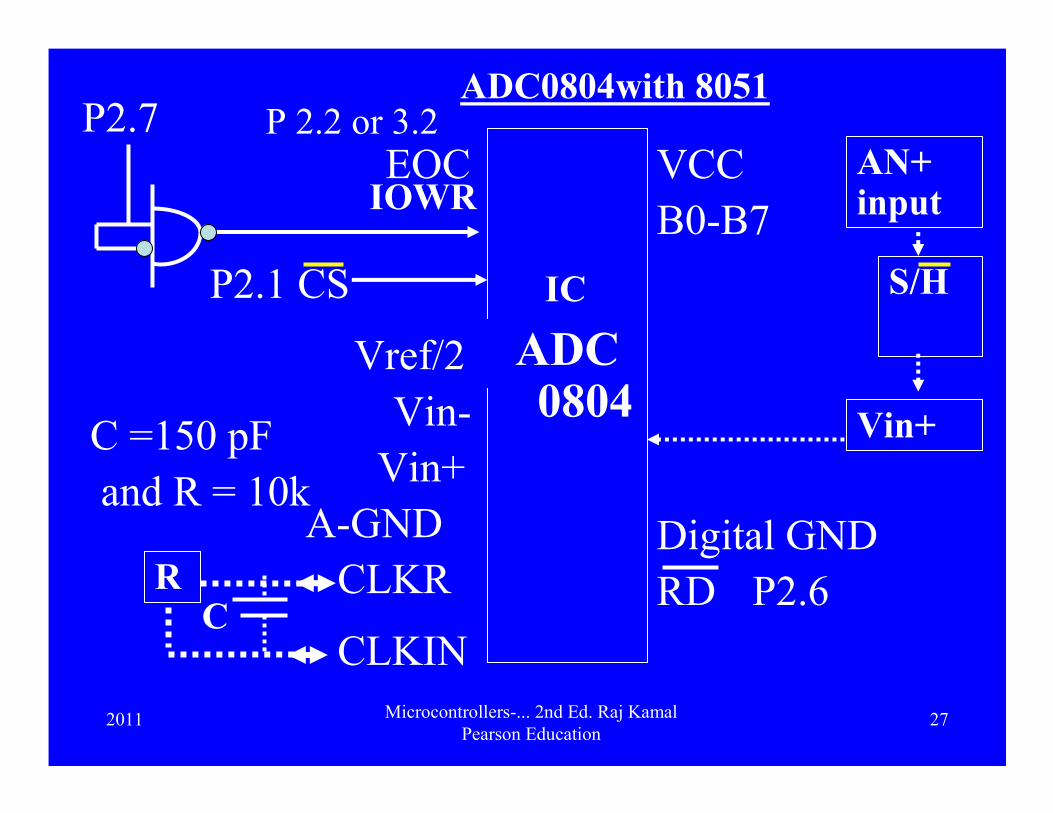
ADC 0804
VCCEOC
CS
Vin-
S/H
Digital GND
RD
B0-B7IOWR
Vref/2
A-GND
CLKIN
CLKR
Vin+
P2.7 P 2.2 or 3.2
P2.1
C =150 pF
and R = 10k
P2.6
IC
AN+ input
Vin+
ADC0804with 8051
RC

2011 Microcontrollers-... 2nd Ed. Raj Kamal
Pearson Education28
2.Select ADC write P2.1 = 0
3. Pulse Start ADC write P2.7 = 1, then P2.7 = 0
5. Reset P2.6 and Read P1
4.Wait till INT0 interrupt or till P2.2
1.Initial condition P2.6 = 1,P2.7 = 1, P3.2 = 1
2011 Microcontrollers-... 2nd Ed. Raj Kamal
Pearson Education29
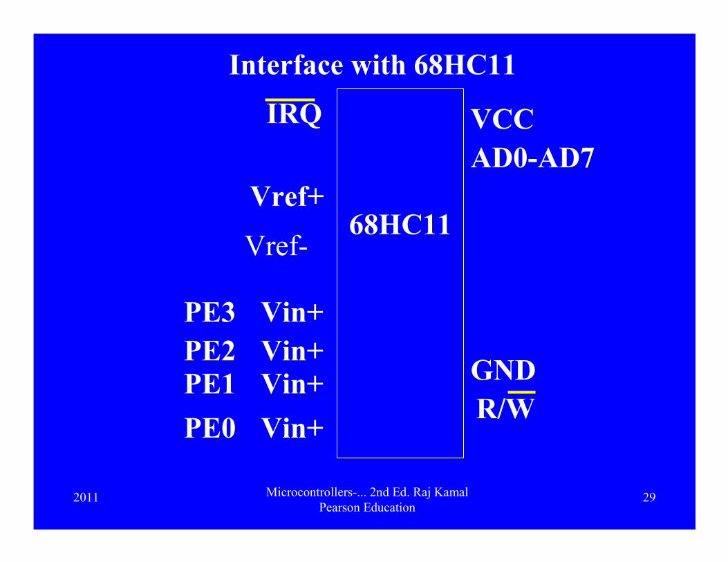
Interface with 68HC11
68HC11
VCCIRQ
Vref+
GND
R/W
AD0-AD7
Vref-
PE0 Vin+
PE1 Vin+
PE2 Vin+
PE3 Vin+

2011 Microcontrollers-... 2nd Ed. Raj Kamal
Pearson Education30
Summary

2011 Microcontrollers-... 2nd Ed. Raj Kamal
Pearson Education31
• ADC Bits at output
• ADC 0804,0808, 0816
• Internal AMUX and channel address latch
• Multi channel ADC
• ADC Interfacing to ports
We learnt
Related Documents