1 Synthesis, Structure and Properties of Boron and Nitrogen Doped Graphene L. S. Panchakarla 1 , K. S. Subrahmanyam 1 , S. K. Saha 2 , A. Govindaraj 1 , H. R. Krishnamurthy 2 , U. V. Waghmare 3* , and C. N. R. Rao 1* 1 Chemistry and Physics of Materials Unit, New Chemistry Unit and CSIR Centre of Excellence in Chemistry, Jawaharlal Nehru Centre for Advanced Scientific Research, Jakkur P.O., Bangalore 560064, India 2 Department of Physics, Indian Institute of Science, Bangalore 560012, India 3 Theoretical Sciences Unit, Jawaharlal Nehru Centre for Advanced Scientific Research, Bangalore 560064, India * email: [email protected] , Fax: (+91) 80-2208 2760, [email protected] Graphene has emerged as an exciting material today because of the novel properties associated with its two-dimensional structure. 1,2 Single-layer graphene is a one-atom thick sheet of carbon atoms densely packed into a two-dimensional honeycomb lattice. It is the mother of all graphitic forms of carbon including zero-dimensional fullerenes and one- dimensional carbon nanotubes. 1 The remarkable feature of graphene is that it is a Dirac solid, with the electron energy being linearly dependent on the wave vector near the vertices of the hexagonal Brillouin zone. It exhibits room-temperature fractional quantum Hall effect 3 and ambipolar electric field effect along with ballistic conduction of charge carriers. 4 It has been reported recently that a top-gated single layer-graphene transistor is able to reach electron or hole doping levels of upto 5x10 13 cm -2 . The doping effects are ideally monitored by Raman spectroscopy. 5-10 Thus, the G band in the Raman spectrum stiffens for both electron and hole doping and the ratio of the intensities of the 2D and G band varies sensitively with doping. Molecular charge-transfer induced by electron-donor and -acceptor molecules also gives rise to significant changes in the electronic structure of few-layer graphenes, as evidenced by

Welcome message from author
This document is posted to help you gain knowledge. Please leave a comment to let me know what you think about it! Share it to your friends and learn new things together.
Transcript
1
Synthesis, Structure and Properties of Boron and Nitrogen Doped
Graphene
L. S. Panchakarla1, K. S. Subrahmanyam1, S. K. Saha2, A. Govindaraj1, H. R.
Krishnamurthy2, U. V. Waghmare3*, and C. N. R. Rao1*
1Chemistry and Physics of Materials Unit, New Chemistry Unit and CSIR Centre of Excellence in Chemistry, Jawaharlal Nehru Centre for Advanced Scientific Research, Jakkur P.O., Bangalore 560064, India
2Department of Physics, Indian Institute of Science, Bangalore 560012, India
3Theoretical Sciences Unit, Jawaharlal Nehru Centre for Advanced Scientific Research, Bangalore 560064, India
*email: [email protected], Fax: (+91) 80-2208 2760, [email protected]
Graphene has emerged as an exciting material today because of the novel properties
associated with its two-dimensional structure.1,2 Single-layer graphene is a one-atom thick
sheet of carbon atoms densely packed into a two-dimensional honeycomb lattice. It is the
mother of all graphitic forms of carbon including zero-dimensional fullerenes and one-
dimensional carbon nanotubes.1 The remarkable feature of graphene is that it is a Dirac solid,
with the electron energy being linearly dependent on the wave vector near the vertices of the
hexagonal Brillouin zone. It exhibits room-temperature fractional quantum Hall effect3 and
ambipolar electric field effect along with ballistic conduction of charge carriers.4 It has been
reported recently that a top-gated single layer-graphene transistor is able to reach electron or
hole doping levels of upto 5x1013 cm-2. The doping effects are ideally monitored by Raman
spectroscopy.5-10 Thus, the G band in the Raman spectrum stiffens for both electron and hole
doping and the ratio of the intensities of the 2D and G band varies sensitively with doping.
Molecular charge-transfer induced by electron-donor and -acceptor molecules also gives rise
to significant changes in the electronic structure of few-layer graphenes, as evidenced by
2
changes in the Raman spectrum.6,7 Charge-transfer by donor and acceptor molecules soften
and stiffen the G band respectively. The difference between electrochemical doping and
doping through molecular charge transfer is noteworthy. It is of fundamental interest to
investigate how these effects compare with the effects of doping graphene by substitution
with boron and nitrogen and to understand dopant-induced perturbations on the properties of
graphene. Secondly, opening of the band-gap in graphene is essential to facilitate its
applications in electronics and graphene bilayers11 are an attractive option for this. With this
motivation, we have prepared, for the first time, B- and N-doped graphene bilayer samples
employing different strategies and investigated their structure and properties. We have also
carried out first-principles DFT calculations to understand the effect of substitutional doping
on the structure of graphene as well as its electronic and vibrational properties.
To prepare B-and N-doped graphenes, we have exploited our recent finding that arc
discharge between carbon electrodes in a hydrogen atmosphere yields graphenes (HG) with
two to three layers. We have prepared B-doped graphene (BG) by two methods involving arc
discharge of graphite electrodes in the presence H2+B2H6 (BG1) and by carrying out arc
discharge using a boron-stuffed graphite electrode (BG2). We have prepared nitrogen-doped
graphene (NG) by carrying out arc discharge in the presence of H2+pyridine (NG1) or
H2+ammonia (NG2). We have also carried out the transformation of nanodiamond in the
presence of pyridine (NG3) to obtain N-doped graphene. All the doped samples were
characterized by variety of physical methods.
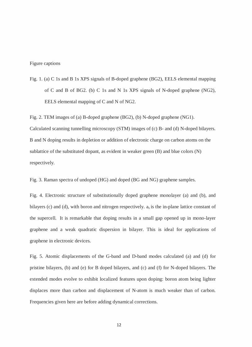
X-ray photoelectron spectroscopic (XPS) analysis showed that the BG1 and BG2
contained 1.2 and 3.1 at% of boron respectively, while the electron energy loss spectroscopy
(EELS) data showed the content of boron in these samples to be 1.0 and 2.4 at% respectively.
In Fig. 1a, we show typical core-level XPS data of BG2 along with the elemental mapping by
EELS. XPS data show NG1, NG2 and NG3 to contain 0.6, 0.9 and 1.4 at% of nitrogen
3
respectively. In Fig. 1b, we have shown XPS data of the NG2 sample along with EELS
elemental mapping. The asymmetric shape of the N 1s peak indicates the existence of at least
two components. On deconvolution, we find peaks at 398.3 eV and 400 eV, the first one
being characteristic of pyridinic nitrogen (sp2 hybridization) and the second of nitrogen in the
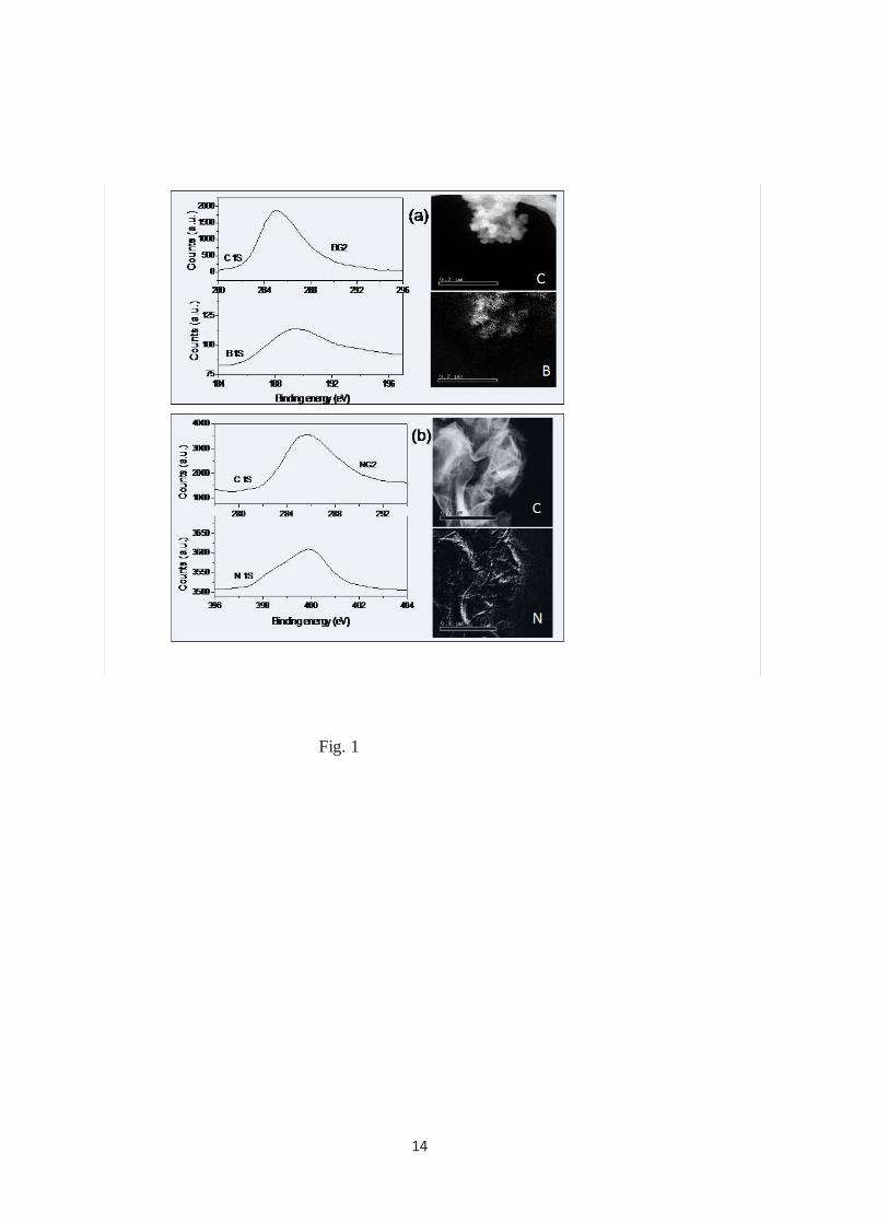
graphene sheets.12,13 Analysis of the (002) reflections in the X-ray diffraction (XRD) patterns
showed that the B-and N-doped samples contained 2-3 layers on an average. This is also
confirmed by the TEM images (see Fig. 2 for typical TEM images). Atomic force microscopy
images also showed the presence of 2-3 layers in the BG and NG samples, with occasional
presence of single layers. TGA shows that the B- and N- doped samples undergo combustion
at a slightly lower temperature than the parent graphene (580 oC).
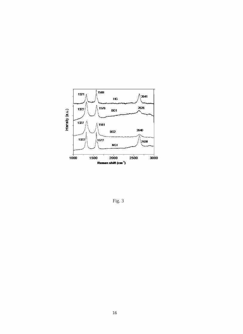
We have examined the Raman spectra of all the BG and NG samples in comparison
with the spectrum of the pure graphene sample (HG), prepared by the H2-discharge method.
We show typical spectra in Fig. 3. The Raman spectrum [with 632.8 nm excitation] of these
samples shows three main features in 1000-3000 cm-1 region, the G band (~ 1570 cm-1 ), the
defect-related D band14 (~ 1320 cm-1 ), and the 2D band(~ 2640 cm-1 ). It is noteworthy that
the G band stiffens both with boron and nitrogen doping. This is similar to what happens with
electrochemical doping.5 The shift in the case of BG2, with a higher B-content, is larger than
with BG1. In the case of N-doped graphene, NG3, with the highest N content, shows the
largest shift. The intensity of the D band is higher with respect to that of the G band in all the
doped samples. On doping, the relative intensity of the 2D band generally decreases with
respect to the G band. We have calculated the in-plane crystallite sizes (La) of the undoped as
well as doped graphene samples by following formula,15
La(nm) = (2.4 X 10⁻¹⁰) λ4 (ID/IG)-1.
Here λ is wavelength used for Raman measurements and ID, IG respectively intensity of D and
G band. The crystallite size of the HG, BG1, BG2, NG1, NG2 and NG3 samples are
4
respectively 64, 30, 26, 43, 41 and 19 nm. Doped graphene samples show low in crystallite
sizes compared to undoped graphene samples. We also find that the BG and NG samples
exhibit much lower electrical resistivity than that of undoped graphene.
We have considered two configurations of doped bi-layer graphene in our simulation (4x4
supercell), where the substituted (3.125%) atoms (B or N at a time) in the two layers are (a)
close to and (b) far from each other. We find that configurations with dopant atoms separated
by larger distance from each other are more favourable energetically. While the configuration
with widely separated N atoms is lower in energy by 25 meV than the one with N at nearest
sites in the two planes, this energy difference for B-substitution is rather small (4 meV). This
implies that homogeneous B-substitution may be easier than N-substitution. The origin of this
difference can be traced to the structure: B-C bond is about 0.5% longer than the C-C bond
while N-C bond is about the same as C-C bond in length, resulting in significant relaxation of
the structure of B-doped bilayer dominating its energetics. The interplanar separation reduces
by almost 2.7% in B-doped bilayer graphene while it remains almost unchanged in N-doped
bilayers. We estimate the energy of formation of doped graphene from graphene and dopant
atoms in the gaseous form to be 5.6 and 8.0 eV/atom for B and N doping respectively,
suggesting that synthesis of B- and N-doped graphene should be quite possible.
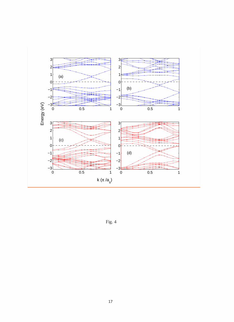
Our calculations reveal that the linearity in the dispersion of the electronic bands within 1eV
of the Fermi-energy is almost unchanged with B- and N-doping (see Fig 4)! This means that
the doped graphenes have the potential to exhibit the interesting properties of pristine
graphenes. Fermi-energy which is at the apex of the conical band-structure near the K-point
of Brillouin zone of graphene, is shifted by -0.65 eV and 0.59 eV in the case of 2 at% B and
N-substitutions. These shifts are of -1.0 and 0.9 eV in 3.125 at% B- and N-doped bilayers
respectively. This results in p-type and n-type semi-conducting behaviour of graphene (see
Fig. 4), as expected. We note that much (96%) of the shift in Fermi energy arises essentially
5
from the substitution with dopants, and the remaining 4% arises from the lattice relaxation.
This is also reflected in the almost symmetric shift in Fermi energy with B- and N-
substitution, which were seen to be associated with large and small structural relaxation
respectively. It is indeed encouraging because this means that effects of doping should scale
reasonably well to lower concentrations.
As Raman spectroscopy is ideally suited for the characterization of doped graphene5-10, it is
important to know how it correlates with the concentration of carriers or dopants. The shift in
the G-band frequency measured by Raman spectroscopy has many physical contributions and
we use our calculations to uncover the relative magnitudes of these. Unexpected purely on
the basis of the lengths of B-C and N-C bonds, in the context of carbon nano-tubes, Yang et
al16 and Coville et al17,18 had reported an interesting finding that the G band shifts are in the
same direction. We demonstrate (see Table I) that indeed the shifts in vibrational frequencies
of graphene with B and N-doping have opposite signs if one takes into account only the
changes in bond-length obtained at fixed lattice constant. Relaxation or the change of lattice
constant is highly asymmetric: the lattice constant increases by 0.32% with 2% boron
substitution in single layer graphene, while it decreases very slightly with N-substitution,
resulting in a large decrease and a slight increase in frequency respectively. With these two
mechanisms alone, the shift in G-band frequency with either B or N substitution is negative,
contrary to our measured trends. After adding the dynamic corrections19-21, these frequency
shifts become positive, in agreement with experimental observations reported here. Very
similar changes in the G-band of bilayer graphene (see Table I) are estimated from our
calculations with B and N substitution, assuming the same amount of dynamic corrections as
in the mono-layer. This assumption is reasonable for shifts in Fermi energy above 0.39 eV
and less than 1 eV (the second band is populated by electrons or holes, as seen in Figure 3),
because the density of states of the bilayer matches with that of the monolayer and hence the
6
dynamic corrections are expected to be similar (see Figs. 3 and 4 in Ref. 18). Thus, the
comparison between experiment and calculations shown here can be used to conclude that
dynamic corrections are important in understanding the changes in the phonon frequencies of
graphene and of bilayers arising from the introduction of carriers. In fact, the overall
neutrality of substitutionally doped graphene allows a very clean and accurate calculation and
further testing of the role of dynamic corrections arising from doping to the G-band in
graphene.
Our observation on the non-segregating tendency or the homogeneity in the distribution of
boron implies that the disorder or the number of possible configurations will increase with the
concentration of dopant atoms and result in more prominent peaks of the D-band, as
evidenced in the measured Raman spectra reported here [see Fig-3]. Secondly, the changes in
frequency of the Raman 2D-band can be understood from our results for the phonons at
K+ΔK accessible in the spectrum of Γ-point phonons, determined for the 4x4 supercell. We
find that the shifts in the frequency of phonons at K+ΔK are comparable to the observed
values (see Table I, lower panel) and much weaker in magnitude than the ones at K, re-
affirming the strong Kohn-anomaly in the phonons at the K-point. We note that the eigen-
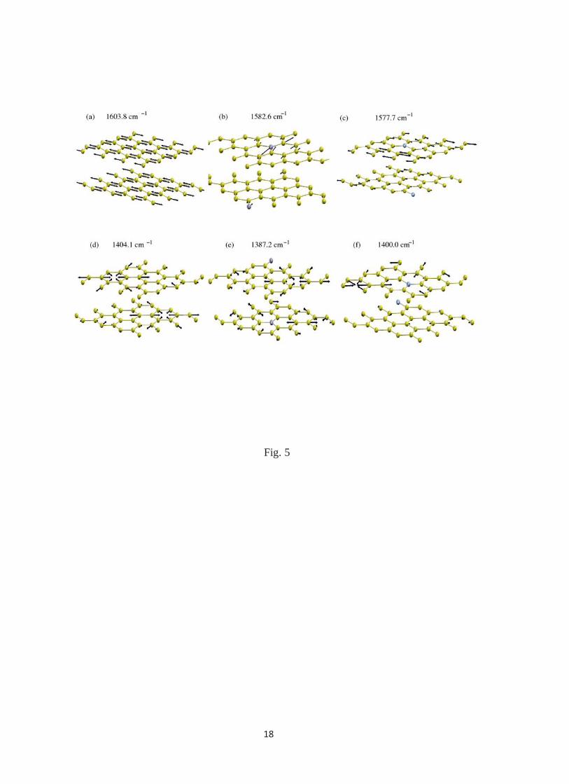
modes of the G-band and D-band (see Figure 5) also change with doping by developing
features in the atomic displacements localized near the dopant atoms, providing a physical
picture why these modes could be used to characterize the nature of dopant atom and its
effects on the electronic structure of graphene or of bilayer-graphene.
Having demonstrated that different routes are possible for synthesis of B and N-doped
graphene, and based on a consistent agreement between our experiments and calculations,
and complementary information derived on the electronic structure, we conclude that B- and
N-doped graphene can be synthesized to exhibit p- and n- type semiconducting electronic
properties that can be systematically tuned with concentration of B and N, and can be
7
characterized with Raman spectroscopy of the G- and D-bands. Realization of such p- and n-
type conducting bilayers should be usable in a variety of devices similar to the ones based on
semiconductors.
Experimental
Synthesis of boron and nitrogen doped graphene: One set of boron doped graphene samples
(BG1) was prepared by carrying out arc discharge of graphite electrodes in the presence of
hydrogen, helium and diborane (B2H6). B2H6 vapor was generated by the addition of BF3-
diethyl etherate to sodium borohydride in tetraglyme. B2H6 vapor was carried to the arc
chamber by passing hydrogen (200 torr) through B2H6 generator and subsequently by passing
He (500 torr). Second set of boron doped samples (BG2) was prepared by carrying out arc
discharge using a boron-stuffed graphite electrode (3 at% boron) in the presence of H2 (200
torr) and He (500 Torr).
One set of nitrogen doped graphene samples (NG1) was prepared by carrying out arc
discharge of graphite electrodes in the presence of H2, He and pyridine vapors. Pyridine
vapour was carried to the arc chamber by passing hydrogen (200 torr) through pyridine
bubbler and subsequently by passing He (500 torr). Second set of nitrogen doped samples
(NG2) was prepared by carrying out arc discharge of graphite electrodes in the presence of
H2 (200 torr), He (200 torr) and NH3 (300 torr). Transformation of nanodiamond was also
carried out in the presence of He and Pyridine vapour at 1650 oC to obtain N-doped graphene
(NG3). We have also carried out the transformation of nanodiamond in the presence of
pyridine (NG3) to obtain N-doped graphene.
Sample characterization: X-ray diffraction (XRD) patterns of the samples were recorded in
the θ-2 θ Bragg-Bretano geometry with a siemens D5005 diffractometer using Cu Kα (λ
=0.151418nm) radiation. Raman spectra were recorded with LabRAM HR high resolution
8
Raman spectrometer (Horiba Jobin Yvon) using He-Ne Laser (λ=632.8 nm). Transmission
electron microscope (TEM) images were obtained with a JEOL JEM 3010 instrument.Atomic
force microscope (AFM) measurements were performed using NanoMan. X-ray
photoelectron spectroscopy (XPS) was recorded using a VG scientific ESCA LAB V
spectrometer. EELS were recorded with a transsmision electron microscope (FEI, TECNAI
F30) equiped with an energy filter for EELS operating at 200kV. Thermogravimetric analysis
was carried out using Mettler Toledo TGA 850 instrument.
Computational Methods: Our first-principles calculations are based on ultra-soft
pseudopotentials and density functional theory as implemented in Quantum Espresso22. The
electron exchange correlation energy has been approximated with the PBE23 form of the
generalized gradient approximation functional for single-layer graphene and the PZ24 form of
the local density approximation functional for bi-layer graphene, as the latter describes the
binding between the two graphene planes more realistically. Doping with B and N was
simulated by replacing one carbon atom in a 5x5 (4x4) supercell, amounting to 2 (3.125)
atomic % substitution in the graphene monolayer (bilayer). In each case, the structure was
fully relaxed to the lowest energy. Kohn-Sham wave functions were expressed in the plane-
wave basis with an energy cut off of 40 Ry and integrations over the Brillouin zones were
sampled with a 9x9x1 (6x6x1 for bilayer) mesh of uniformly-spaced k-points. Vibrational
properties were determined using density functional theory linear response formalism within
the adiabatic approximation, and further dynamic corrections were obtained using the time-
dependent perturbation theory20 and the linear form of electronic band dispersion at the Fermi
level. Our methodology and calculational parameters have been tested for convergence
before.25,26
9
Acknowledgements
L.S.P. and K.S.S. gratefully acknowledge CSIR, New Delhi, for a senior research fellowship
and S.K.S. acknowledges financial support from the JNCASR. We would also like to
acknowledge use of central computing facility from the Centre for Computational Materials
Science at JNCASR.
10
References
[1] A. K. Geim and K. S. Novoselov, Nature Mater. 2007, 6, 183.
[2] M. I. Katsnelson, Materials Today 2007, 10, 20.
[3] K. S. Novoselov, Z. Jiang, Y. Zhang, S. V. Morozov, H. L. Stormer, U. Zeitler, J. C.
Maan, G. S. Boebinger, P. Kim and A. K. Geim, Science 2007, 315, 1379.
[4] K. S. Novoselov, A. K. Geim, S. V. Morozov, D. Jiang, Y. Zhang, S. V. Dubonos, I.
V. Grigorieva and A. A. Firsov, Science 2004, 306, 666.
[5] A. Das, S. Pisana, B. Chakraborty, S. Piscanec, S. K. Saha, U. V. Waghmare, K. S.
Novoselov, H. R. Krishnamurthy, A. K. Geim, A. C. Ferrari and A. K. Sood, Nature
Nanotech. 2008, 3, 210.
[6] B. Das, R. Voggu, C. S. Rout and C. N. R. Rao, Chem. Comm. 2008, 5155.
[7] R. Voggu, B. Das, C. S. Rout and C. N. R. Rao, J. Phys.: Condens. Matter 2008, 20,
472204.
[8] A. C. Ferrari, J. C. Meyer, V. Scardaci, C. Casiraghi, M. Lazzeri, F. Mauri, S. Piscanec,
D. Jiang, K. S. Novoselov, S. Roth, and A. K. Geim, Phys. Rev. Lett. 2006, 97, 187401.
[9] A. C. Ferrari, Solid State Commun. 2007, 143, 47.
[10] K. S. Subrahmanyam, S. R. C. Vivekchand, A. Govindaraj, and C. N. R. Rao, J.
Matert. Chem. 2008, 13, 1517.
[11] T. Ohta, A. Bostwick, T. Seyller, K. Horn, E. Rotenberg, Science 2006, 313, 951.
[12] L. S. Panchakarla, A. Govindraj and C. N. R. Rao, ACS Nano 2007, 1, 494.
11
[13] R. Sen, B. C. Satishkumar, A. Govindaraj, K. R. Harikumar, G. Raina, J. –P. Zhang,
A. K. Cheetham, C. N. R. Rao, Chem. Phys. Lett. 1998, 287, 671.
[14] M. S. Dresselhaus, P. C. Eklund, Advances in Physics 2000, 49, 705.
[15] L. G. Cançado, K. Takai, T. Enoki, M. Endo, Y. A. Kim, H. Mizusaki, A. Jorio, L. N.
Coelho, R. M. Paniago, and M. A. Pimenta, Appl. Phys. Lett. 2006, 88, 163106.
[16] Q. Yang, P. Hou, M. Unno, S. Yamauchi, R. Saito, and T. Kyotani, Nano Lett. 2005, 5,
2465.
[17] K. C. Mondal, A. M. Strydom, R. M. Erasmus, J. M. Keartland, N. J. Coville, Mater.
Chem. Phys. 2008, 111, 386.
[18] E. N. Nxumalo, V. O Nyamori, N. J Coville, J. Organomet. Chem. 2008, 692, 2942.
[19] T. Ando, J. Phys. Soc. Jpn. 2006, 75, 124701.
[20] M. Lazzeri, and F. Mauri, Phys. Rev.Lett. 2006, 97, 266407.
[21] T. Ando, J. Phys. Soc. Jpn. 2007, 76, 104711.
[22] S. Baroni, S. de Gironcoli, A. Dal Corso, and P. Giannozzi, http://www.pwscf.org.
[23] J. P. Perdew, K. Burke, and M. Ernzerhof, Phys. Rev. Lett. 1996, 77, 3865.
[24] J. P. Perdew and A. Zunger, Phys. Rev. B 1981, 23, 5048.
[25] S. K. Saha, U. V. Waghmare, H. R. Krishnamurthy, and A. K. Sood, Phys. Rev. B
2007, 76, 201404.
[26] S. K. Saha, U. V. Waghmare, H. R. Krishnamurthy, and A. K. Sood, Phys. Rev. B,
2008, 78, 165421.
12
Figure captions
Fig. 1. (a) C 1s and B 1s XPS signals of B-doped graphene (BG2), EELS elemental mapping
of C and B of BG2. (b) C 1s and N 1s XPS signals of N-doped graphene (NG2),
EELS elemental mapping of C and N of NG2.
Fig. 2. TEM images of (a) B-doped graphene (BG2), (b) N-doped graphene (NG1).
Calculated scanning tunnelling microscopy (STM) images of (c) B- and (d) N-doped bilayers.
B and N doping results in depletion or addition of electronic charge on carbon atoms on the
sublattice of the substituted dopant, as evident in weaker green (B) and blue colors (N)
respectively.
Fig. 3. Raman spectra of undoped (HG) and doped (BG and NG) graphene samples.
Fig. 4. Electronic structure of substitutionally doped graphene monolayer (a) and (b), and
bilayers (c) and (d), with boron and nitrogen respectively. as is the in-plane lattice constant of
the supercell. It is remarkable that doping results in a small gap opened up in mono-layer
graphene and a weak quadratic dispersion in bilayer. This is ideal for applications of
graphene in electronic devices.
Fig. 5. Atomic displacements of the G-band and D-band modes calculated (a) and (d) for
pristine bilayers, (b) and (e) for B doped bilayers, and (c) and (f) for N-doped bilayers. The
extended modes evolve to exhibit localized features upon doping: boron atom being lighter
displaces more than carbon and displacement of N-atom is much weaker than of carbon.
Frequencies given here are before adding dynamical corrections.
13
Table I: Various contributions to the shifts in phonon frequencies of graphene and bilayers resulting from B or N substitution. “Fixed lattice” means internally relaxed structure keeping the lattice constant the same as of undoped system; “Relaxed lattice” means the lattice constant is also relaxed for doped configurations. Dynamic corrections are obtained using formalism in Refs. 19 and 20.
G-band Fixed lattice Relaxed lattice With dynamic
correction
Pristine monolayer graphene
1570.7 1570.7 1570.7
2% Boron doped monolayer
1579.4 1561.2 1584.6
2% Nitrogen doped monolayer
1546.5 1553.4 1574.4
Pristine bilayer graphene
1603.8 1603.8 1603.8
3.125% Boron doped bilayer
1609.7 1582.4 1617.8
3.125% Nitrogen doped bilayer
1566.1 1577.7 1609.9
D-bands Frequency (cm-1) D-band
shift (cm-1) 2D-band
shift (cm-1)
Pristine bilayer graphene
1404.1 0.0 0.0
3.125% Boron doped bilayer
1387.2 -16.9 -33.2
3.125% Nitrogen doped bilayer
1400.0 -4.1 -8.2
14
Fig. 1
15
Fig. 2
16
Fig. 3
17
0 0.5 1−3
−2
−1
0
1
2
3
(a)
Ene
rgy
(eV
)
0 0.5 1−3
−2
−1
0
1
2
3
(b)
0 0.5 1−3
−2
−1
0
1
2
3
(c)
0 0.5 1−3
−2
−1
0
1
2
3
(d)
k (π /as)
Fig. 4
18
Fig. 5
19
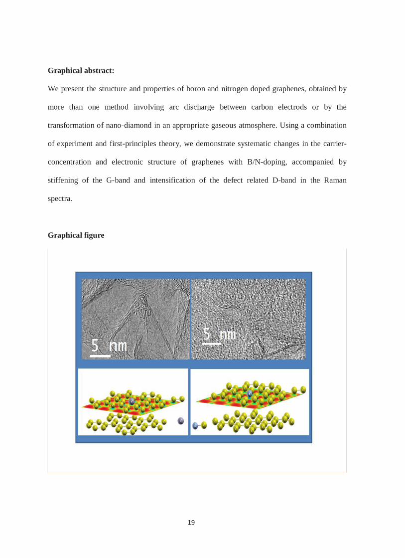
Graphical abstract:
We present the structure and properties of boron and nitrogen doped graphenes, obtained by
more than one method involving arc discharge between carbon electrods or by the
transformation of nano-diamond in an appropriate gaseous atmosphere. Using a combination
of experiment and first-principles theory, we demonstrate systematic changes in the carrier-
concentration and electronic structure of graphenes with B/N-doping, accompanied by
stiffening of the G-band and intensification of the defect related D-band in the Raman
spectra.
Graphical figure
Related Documents