Synthesis of rare-earth doped ZnO nanorods and their defect–dopant correlated enhanced visible- orange luminescence† A. Layek, * S. Banerjee, B. Manna and A. Chowdhury We report the synthesis of size controlled ZnO and rare-earth doped ZnO nanorods in the sub-10 nm diameter regime. The preferential anisotropic growth of the nanostructures along the polar c-axis leads to the formation of wurtzite phase ZnO nanorods. Photoluminescence measurements reveal enhancement of visible luminescence intensity with increasing RE 3+ concentrations upon excitation of host ZnO into the band gap. The broad visible luminescence originates from multiple intrinsic or extrinsic defects. The luminescence from RE 3+ is enabled by energy transfer from defect centers of the host nanocrystal lattice to dopant sites. Host–guest energy transfer facilitates efficient intra-4f orbital transitions ( 5 D 4 / 7 F j for Tb 3+ and 5 D 0 / 7 F j for Eu 3+ ) related characteristic green or red emission. Interestingly, different decay rates of host defects and RE 3+ emission transition also allow temporal control to achieve either pure green or red color. This study suggests that manipulation of defects through bottom-up techniques is a viable method to modulate the energy transfer dynamics, which may help enable the future applications of ZnO-based phosphor materials in optoelectronic and multicolor emission displays. 1. Introduction Zinc oxide (ZnO) has attracted great research interests due to its wide and direct band gap (3.37 eV), 1 large exciton binding energy (60 meV), 1 and extensive applications in piezoelectric transducers, 2 chemical and gas sensors, 3 optical waveguides, 4 transparent conductive lms, 5 varistors, 6 spintronics, 7 and solar cell windows. 8,9 The decisive roles of shapes and sizes on the physical and chemical properties of semiconducting materials have already been established. 10–12 Thus, considerable attention has been drawn towards the design of different surface morphologies of ZnO nanostructures; e.g., nanowires, 13 nano- rods, 14,15 nanobelts, 16 nanotubes, 17 and nanohelices. 18 Apart from the available various morphologies, cost effectiveness, thermal and chemical stability and environmentally benign nature makes ZnO a popular choice for optical devices. For ZnO, there are typically two emission bands. One is centred in the UV region; the other is centred in the visible region. The UV emission is well-known to be associated with the radiative recombination of electron from conduction band with hole from valence band. Although the origin of the visible luminescence is controversial till date, however, it has been attributed to interstitial zinc (Zn i ), oxygen vacancies (V o ), chemisorbed oxygen, copper impurities, and zinc vacancies etc. 19–21 Even though the visible emission in ZnO is undesirable for near-UV emitting devices, however, most recent work by Radovanovic and co-workers has proposed an excellent model for utilization of robustly broad luminescence of ZnO in light emitting diodes. 22 It fuels our interest to further explore avenues for enhancing the photoluminescence by doping rare earth ions (RE 3+ ) into ZnO. It is well known RE 3+ emits in visible-IR region consisting of stable, sharp multiple bands at single excitation. However, it is very challenging to incorporate RE 3+ into ZnO lattice because of giant difference in ionic radii and charge, 23,24 which propels intrinsic self-purication process in the host. 25,26 Nevertheless, attempts have been made for the generation of orange-red emission from ZnO nanomaterials by doping impurity, surface defects or trap states in the host materials. 27–29 The luminescence intensities of RE 3+ are oen observed to be insufficiently low even aer successful incorporation in the ZnO host. 30 This may be due to very rapid excitonic decay of ZnO, 31 which inhibits direct energy transfer to RE ions; and the quenching of RE emission due to nonradiative transfer from RE 3+ ion to ZnO host. 32 Nonetheless, it remains an open ques- tion regarding the dynamics of transfer process and optimiza- tion of visible luminescence efficiency by manipulating defect– dopant interactions. Therefore, it requires further investiga- tions in this area for better understanding and technological developments. Department of Chemistry, Indian Institute of Technology Bombay, Mumbai 400076, India. E-mail: [email protected] † Electronic supplementary information (ESI) available: XRD pattern showing peak shi for Tb 3+ and Eu 3+ doped nanorods, estimated doping concentration of rare earth ions in nanorods, PL decay and tables listing decay parameters for rare earth doped ZnO nanorods. See DOI: 10.1039/c6ra02278b Cite this: RSC Adv. , 2016, 6, 35892 Received 25th January 2016 Accepted 30th March 2016 DOI: 10.1039/c6ra02278b www.rsc.org/advances 35892 | RSC Adv., 2016, 6, 35892–35900 This journal is © The Royal Society of Chemistry 2016 RSC Advances PAPER Published on 01 April 2016. Downloaded by INDIAN INSTITUTE OF TECHNOLOGY BOMBAY on 02/07/2016 10:24:39. View Article Online View Journal | View Issue

Welcome message from author
This document is posted to help you gain knowledge. Please leave a comment to let me know what you think about it! Share it to your friends and learn new things together.
Transcript
RSC Advances
PAPER
Publ
ishe
d on
01
Apr
il 20
16. D
ownl
oade
d by
IN
DIA
N I
NST
ITU
TE
OF
TE
CH
NO
LO
GY
BO
MB
AY
on
02/0
7/20
16 1
0:24
:39.
View Article OnlineView Journal | View Issue
Synthesis of rare
Department of Chemistry, Indian Institute
India. E-mail: [email protected]
† Electronic supplementary informationpeak shi for Tb3+ and Eu3+ doped nanoof rare earth ions in nanorods, PL decayrare earth doped ZnO nanorods. See DOI:
Cite this: RSC Adv., 2016, 6, 35892
Received 25th January 2016Accepted 30th March 2016
DOI: 10.1039/c6ra02278b
www.rsc.org/advances
35892 | RSC Adv., 2016, 6, 35892–359
-earth doped ZnO nanorods andtheir defect–dopant correlated enhanced visible-orange luminescence†
A. Layek,* S. Banerjee, B. Manna and A. Chowdhury
We report the synthesis of size controlled ZnO and rare-earth doped ZnO nanorods in the sub-10 nm
diameter regime. The preferential anisotropic growth of the nanostructures along the polar c-axis leads
to the formation of wurtzite phase ZnO nanorods. Photoluminescence measurements reveal
enhancement of visible luminescence intensity with increasing RE3+ concentrations upon excitation of
host ZnO into the band gap. The broad visible luminescence originates from multiple intrinsic or
extrinsic defects. The luminescence from RE3+ is enabled by energy transfer from defect centers of the
host nanocrystal lattice to dopant sites. Host–guest energy transfer facilitates efficient intra-4f orbital
transitions (5D4 / 7Fj for Tb3+ and 5D0 / 7Fj for Eu3+) related characteristic green or red emission.
Interestingly, different decay rates of host defects and RE3+ emission transition also allow temporal
control to achieve either pure green or red color. This study suggests that manipulation of defects
through bottom-up techniques is a viable method to modulate the energy transfer dynamics, which may
help enable the future applications of ZnO-based phosphor materials in optoelectronic and multicolor
emission displays.
1. Introduction
Zinc oxide (ZnO) has attracted great research interests due to itswide and direct band gap (3.37 eV),1 large exciton bindingenergy (60 meV),1 and extensive applications in piezoelectrictransducers,2 chemical and gas sensors,3 optical waveguides,4
transparent conductive lms,5 varistors,6 spintronics,7 and solarcell windows.8,9 The decisive roles of shapes and sizes on thephysical and chemical properties of semiconducting materialshave already been established.10–12 Thus, considerable attentionhas been drawn towards the design of different surfacemorphologies of ZnO nanostructures; e.g., nanowires,13 nano-rods,14,15 nanobelts,16 nanotubes,17 and nanohelices.18 Apartfrom the available various morphologies, cost effectiveness,thermal and chemical stability and environmentally benignnature makes ZnO a popular choice for optical devices.
For ZnO, there are typically two emission bands. One iscentred in the UV region; the other is centred in the visibleregion. The UV emission is well-known to be associated with theradiative recombination of electron from conduction band withhole from valence band. Although the origin of the visible
of Technology Bombay, Mumbai 400076,
(ESI) available: XRD pattern showingrods, estimated doping concentrationand tables listing decay parameters for10.1039/c6ra02278b
00
luminescence is controversial till date, however, it has beenattributed to interstitial zinc (Zni), oxygen vacancies (Vo),chemisorbed oxygen, copper impurities, and zinc vacanciesetc.19–21 Even though the visible emission in ZnO is undesirablefor near-UV emitting devices, however, most recent work byRadovanovic and co-workers has proposed an excellent modelfor utilization of robustly broad luminescence of ZnO in lightemitting diodes.22 It fuels our interest to further explore avenuesfor enhancing the photoluminescence by doping rare earth ions(RE3+) into ZnO. It is well known RE3+ emits in visible-IR regionconsisting of stable, sharp multiple bands at single excitation.However, it is very challenging to incorporate RE3+ into ZnOlattice because of giant difference in ionic radii and charge,23,24
which propels intrinsic self-purication process in the host.25,26
Nevertheless, attempts have been made for the generation oforange-red emission from ZnO nanomaterials by dopingimpurity, surface defects or trap states in the host materials.27–29
The luminescence intensities of RE3+ are oen observed to beinsufficiently low even aer successful incorporation in the ZnOhost.30 This may be due to very rapid excitonic decay of ZnO,31
which inhibits direct energy transfer to RE ions; and thequenching of RE emission due to nonradiative transfer fromRE3+ ion to ZnO host.32 Nonetheless, it remains an open ques-tion regarding the dynamics of transfer process and optimiza-tion of visible luminescence efficiency by manipulating defect–dopant interactions. Therefore, it requires further investiga-tions in this area for better understanding and technologicaldevelopments.
This journal is © The Royal Society of Chemistry 2016
Paper RSC Advances
Publ
ishe
d on
01
Apr
il 20
16. D
ownl
oade
d by
IN
DIA
N I
NST
ITU
TE
OF
TE
CH
NO
LO
GY
BO
MB
AY
on
02/0
7/20
16 1
0:24
:39.
View Article Online
In this article, we report the synthesis and optical propertiesof RE3+ doped ZnO nanorods of sub-10 nm diameter regime.RE3+ doped nanorods show very narrow size distribution andtheir length depends on the growth time. The wurtzite phaseZnO anisotropically grow along the c-axis which has high energypolar surfaces. Photoluminescence (PL) measurements revealenhancement of visible luminescence intensity with increasingRE3+ concentrations upon excitation of host ZnO into band gap,indicating possible energy transfer into dopant energy levelfrom the host. Upon excitation into ZnO band, the appearanceof characteristic intra-4f orbital transitions of RE3+ indicateshost–guest energy transfer, likely involving the ZnO defectstates. Time resolved photoluminescence (TRPL) decays recor-ded for RE3+ doped ZnO nanorods in current studies are noticedto be signicantly slower than undoped nanorods, whichfurther supports that the deep defects in ZnO serve as energytraps and pave the way for effective energy transfer to dopedRE3+ ions and their relevant light emissions. Our results indi-cate that chemical manipulation of defect–dopant interactionsprovide attractive path to achieve multicolour emission in RE3+-doped ZnO and may nd applications in photonics, lightemitting devices, and displays.
2. Experimental2.1. Preparation of ZnO nanorods
Undoped ZnO nanorods were synthesized by hydrothermalprocess in which ZnO nanoparticles were used as seed nuclei forthe growth of nanorods following an experimental methodprescribed by Xu et al.12 In the rst step, ZnO nanoparticles weresynthesized by sol–gel method.33 Briey, a solution of potas-sium hydroxide (KOH) (Merck, 85%) (�3.4 mM) in MeOH(Spectrochem, Mumbai India, 99.8%) was reuxed at 60 �C for45 min. An ultrasonically dissolved solution of zinc acetatedihydrate (Zn(OAc)2$2H2O) (Loba Chemie Pvt. Ltd., 98%) (�1.4mM) in MeOH was added drop wise to the reuxing KOHsolution at 60 �C. Entire mixture was rigorously stirred for 10min to produce ZnO sols. The as prepared sol was taken inTeon lined autoclave for the growth of undoped ZnO nano-rods. The autoclave was sealed and heated at 120 �C for 4 h andthen cooled at room temperature overnight. The precipitatedsample was centrifuged and washed several times with Milli-pore water to remove any un-reacted precursors. Finally, thewashed sample was dried at 50 �C in air oven for 24 h.
2.2. Preparation of RE3+ doped ZnO nanorods
An equimolar mixture of zinc nitrate hexahydrate (Zn(NO3)2-$6H2O) (Merck, 96%) and hexamethylenetetramine (HMT)(C6H12N4) (Analytical Rasayan, S D Fine-Chem Ltd., 99.5%) (1.0mM) was dissolved in Millipore water. For RE3+ doping,aqueous solutions of terbium or europium nitrate pentahydrate(RE(NO3)3$5H2O) (Sigma Aldrich 99.9%) were added to abovemixture of Zn(NO3)2 and HMT. RE(NO3)3 of 10 weight%, 20weight%, 30 weight% and 40 weight% of Zn(NO3)2 were used fordoping. In the second step, 60 mL of rare earth containingcomplex mixture was directly added to 2 mL as-prepared ZnO
This journal is © The Royal Society of Chemistry 2016
sols in Teon lined autoclave. The autoclave was sealed andheated at 120 �C for 4 h and then cooled at room temperatureovernight. The precipitated sample was treated in similarfashion as described for undoped ZnO nanorods.
2.3. Sample preparation for spectroscopic studies
Doped or undoped ZnO nanorods of were dispersed in 3 mL ofMeOH. Before solution phase spectroscopic studies, individualdispersions were sonicated for 5 min to assure the dissolutionof all solid residue. For solid state PL, the dispersed nanorodswere coated on a spectroscopically cleaned Si wafer.
2.4. Equipments
Different phases in nanostructures were identied by X-raydiffraction studies using Philips powder diffractometer PW3040/60 with Cu Ka radiation (l ¼ 1.540 A). The chemical composi-tions of as-prepared samples were examined with an energydispersive X-ray spectrometer (Oxford INCA Energy TEM 200EDS). Transmission electron microscopic images were recordedwith a high resolution transmission electron microscope (JEOLJEM 2100/Philips CM 200) at an accelerating voltage 200 kV.
All absorption spectra were recorded with an absorptionspectrophotometer (JASCO-V 530) using a quartz cuvette of 1 cmpath at room temperature. All absorption spectra were recordedin the wavelength region of 250 nm to 500 nm length. Steady-state PL measurements were performed using a uorescencespectrophotometer (Varian Carry Eclipse) with CW-xenon lampexcitation at the excitation wavelength of 325 nm. All PL spectrawere recorded in the wavelength region of 350 nm to 750 nmand the slit widths for both excitation and emission mono-chromator were set to 5 nm. Time delayed PL spectra wererecorded with delay time 0.1 ms and gate time 5 ms. In the solidstate PL experiment, a He–Cd laser source (325 nm) was used forthe excitation and an Acton monochromator attached witha cooled CCD camera was used to record the spectra. Lowtemperature PL measurements at 10 K were also performedusing the same PL setup and a closed cycle He-refrigerator.
Time-resolved luminescence studies were performed usinga time correlated single photon-counting (TCSPC) system fromIBH, UK to measurer lifetimes in ns time range. The excitationsource was a 340 nm light emitting diode with full width halfmaximum of 800 ps. Decays were at the emission wavelengths of520 nm, 540 nm and 580 nm with an emission polarizer ata magic angle of 54.7�. The slit width for the emission mono-chromator was 8 nm. The intensity for the channel withmaximum intensity was 10 000 counts. The instrumentresponse function (IRF) was recorded using Ludox solution(Sigma Aldrich) by detecting the scattered emission at theexcitation wavelength.
An iterative reconvolution method was employed to analyzeall decays using IBH DAS 6.2 soware. An experimental curvewas t to a program generated calculated curve, which wasconvoluted numerically with the instrument response function.
Decays were t to a model of sum of two-exponentials usingthe IBH DAS-6 program.
RSC Adv., 2016, 6, 35892–35900 | 35893
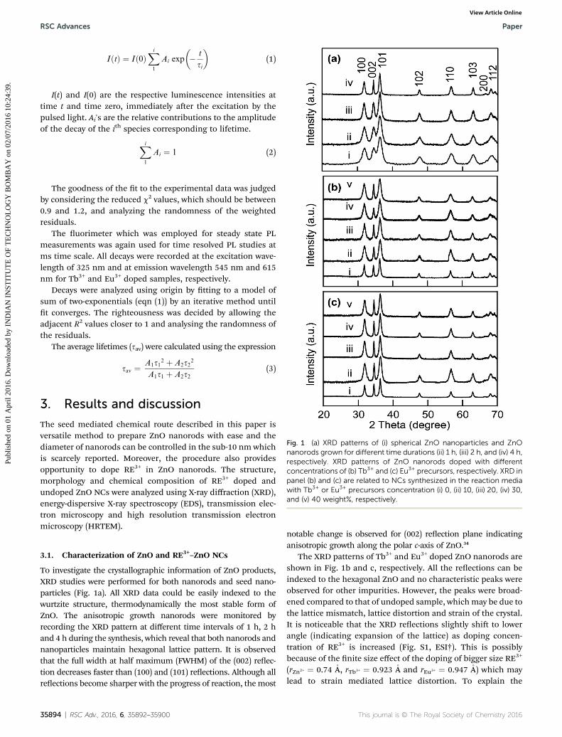
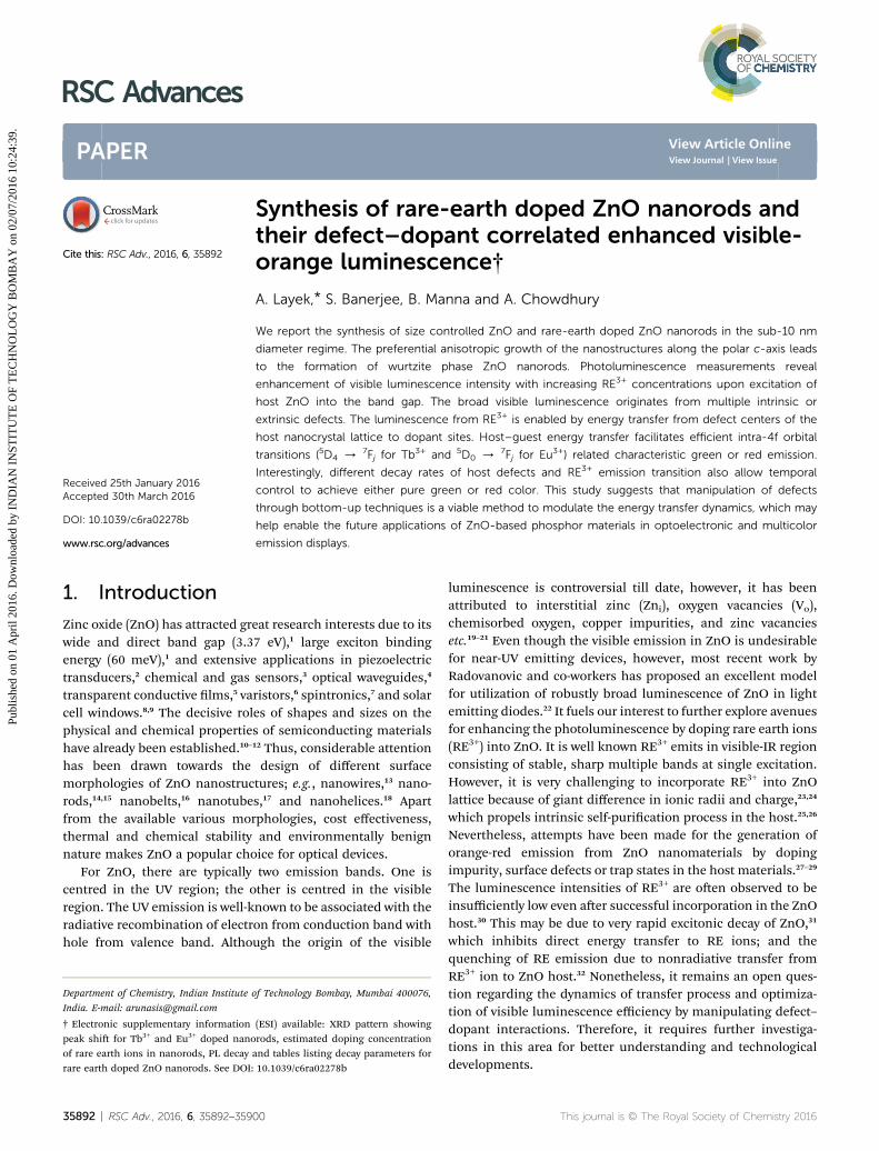
Fig. 1 (a) XRD patterns of (i) spherical ZnO nanoparticles and ZnOnanorods grown for different time durations (ii) 1 h, (iii) 2 h, and (iv) 4 h,respectively. XRD patterns of ZnO nanorods doped with differentconcentrations of (b) Tb3+ and (c) Eu3+ precursors, respectively. XRD inpanel (b) and (c) are related to NCs synthesized in the reaction mediawith Tb3+ or Eu3+ precursors concentration (i) 0, (ii) 10, (iii) 20, (iv) 30,and (v) 40 weight%, respectively.
RSC Advances Paper
Publ
ishe
d on
01
Apr
il 20
16. D
ownl
oade
d by
IN
DIA
N I
NST
ITU
TE
OF
TE
CH
NO
LO
GY
BO
MB
AY
on
02/0
7/20
16 1
0:24
:39.
View Article Online
IðtÞ ¼ Ið0ÞXi
1
Ai exp
�� t
si
�(1)
I(t) and I(0) are the respective luminescence intensities attime t and time zero, immediately aer the excitation by thepulsed light. Ai's are the relative contributions to the amplitudeof the decay of the ith species corresponding to lifetime.
Xi
1
Ai ¼ 1 (2)
The goodness of the t to the experimental data was judgedby considering the reduced c2 values, which should be between0.9 and 1.2, and analyzing the randomness of the weightedresiduals.
The uorimeter which was employed for steady state PLmeasurements was again used for time resolved PL studies atms time scale. All decays were recorded at the excitation wave-length of 325 nm and at emission wavelength 545 nm and 615nm for Tb3+ and Eu3+ doped samples, respectively.
Decays were analyzed using origin by tting to a model ofsum of two-exponentials (eqn (1)) by an iterative method untilt converges. The righteousness was decided by allowing theadjacent R2 values closer to 1 and analysing the randomness ofthe residuals.
The average lifetimes (sav) were calculated using the expression
sav ¼ A1s12 þ A2s22
A1s1 þ A2s2(3)
3. Results and discussion
The seed mediated chemical route described in this paper isversatile method to prepare ZnO nanorods with ease and thediameter of nanorods can be controlled in the sub-10 nm whichis scarcely reported. Moreover, the procedure also providesopportunity to dope RE3+ in ZnO nanorods. The structure,morphology and chemical composition of RE3+ doped andundoped ZnO NCs were analyzed using X-ray diffraction (XRD),energy-dispersive X-ray spectroscopy (EDS), transmission elec-tron microscopy and high resolution transmission electronmicroscopy (HRTEM).
3.1. Characterization of ZnO and RE3+–ZnO NCs
To investigate the crystallographic information of ZnO products,XRD studies were performed for both nanorods and seed nano-particles (Fig. 1a). All XRD data could be easily indexed to thewurtzite structure, thermodynamically the most stable form ofZnO. The anisotropic growth nanorods were monitored byrecording the XRD pattern at different time intervals of 1 h, 2 hand 4 h during the synthesis, which reveal that both nanorods andnanoparticles maintain hexagonal lattice pattern. It is observedthat the full width at half maximum (FWHM) of the (002) reec-tion decreases faster than (100) and (101) reections. Although allreections become sharper with the progress of reaction, themost
35894 | RSC Adv., 2016, 6, 35892–35900
notable change is observed for (002) reection plane indicatinganisotropic growth along the polar c-axis of ZnO.34
The XRD patterns of Tb3+ and Eu3+ doped ZnO nanorods areshown in Fig. 1b and c, respectively. All the reections can beindexed to the hexagonal ZnO and no characteristic peaks wereobserved for other impurities. However, the peaks were broad-ened compared to that of undoped sample, whichmay be due tothe lattice mismatch, lattice distortion and strain of the crystal.It is noticeable that the XRD reections slightly shi to lowerangle (indicating expansion of the lattice) as doping concen-tration of RE3+ is increased (Fig. S1, ESI†). This is possiblybecause of the nite size effect of the doping of bigger size RE3+
(rZn2+ ¼ 0.74 �A, rTb3+ ¼ 0.923 �A and rEu3+ ¼ 0.947 �A) which maylead to strain mediated lattice distortion. To explain the
This journal is © The Royal Society of Chemistry 2016
Paper RSC Advances
Publ
ishe
d on
01
Apr
il 20
16. D
ownl
oade
d by
IN
DIA
N I
NST
ITU
TE
OF
TE
CH
NO
LO
GY
BO
MB
AY
on
02/0
7/20
16 1
0:24
:39.
View Article Online
dopant–defect induced broadening of XRD line prole we per-formed Williamson–Hall (W–H) analysis of ZnO nanorods(Fig. S2, ESI†). It is known that average crystallite size and strainin the NPs can be calculated from the spectral line shape usingW–H plot based on the equation
b cos qhkl ¼ 0:9l
Dþ 43 sin qhkl (4)
where, b, qhkl, l, D, and 3 represent FWHM of the XRD reection,Bragg's angle, wavelength of X-ray¼ 0.1540 nm, average particlesize diameter, and strain, respectively. Assuming isotropicstrain deformation model would show linear behaviour whenplotted b cos qhkl vs. 4 sin qhkl and slope to the linear t wouldindicate the strain (3). However, we found that the W–H analysisof RE3+ doped nanorods display scatter data points (Fig. S2,ESI†). Nonlinear nature of the W–H plot clearly indicates thatXRD line broadening is due to anisotropic strain in ZnOnanorods.35 Qualitatively, it is noted that increase in dopantconcentration induces more strain in the nanorods.
To elucidate the morphologies of the undoped and RE3+
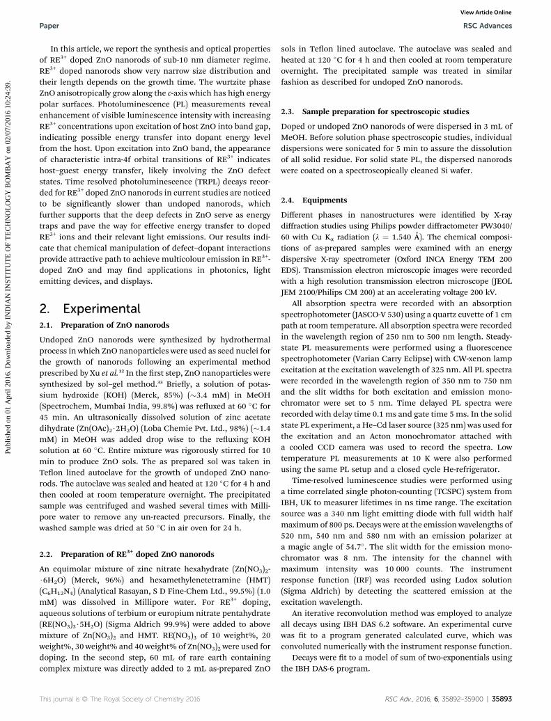
doped nanorods, we performed TEM measurements. The TEMimages of undoped ZnO nanorods were recorded at differenttime point of nanorod growth as shown in Fig. 2a–c. It shouldbe noted that the length of the nanorods are less than 50 nmalong with many small elongated nanoparticles when thereaction was allowed to proceed for 1 h (Fig. 2a). The aspectratio, l/d (length/diameter) of nanorods grown for 2 h was foundto be larger (Fig. 2b) than nanorods grown for 1 h. The averagelengths of the nanorods grown for 4 h were found to be 50–100nm with diameter (10 � 2 nm) (Fig. 2c). It is interesting to notethat the average length of the nanorods increases with theprogress of reaction, however, the diameter of the nanorodsremain unchanged. This observation has oen been explainedby oriented attachment (OA) growth model.34,36 However, in ourcase, there is not ample evidence to support the OA mechanismbecause no oriented attachment of particles has been found byHRTEM except at the primary stage of growth. Here, we proposethat when a ZnO nucleus is newly formed, owing to the high
Fig. 2 TEM images of ZnO nanorods allowed to grow for time dura-tion (a) 1 h, (b) 2 h, and (c) 4 h, respectively. (d) The HRTEM image ofZnO nanorods shows lattice fringes with diameter � 10 nm. Arrow-heads indicates anisotropic growth of undoped nanorods occurringalong [0001] direction.
This journal is © The Royal Society of Chemistry 2016
energy polar surfaces, the incoming precursor molecules tendto favorably adsorb on the polar surfaces in order to minimizethe total energy of the system.37 However, aer adsorption ofone layer of precursor molecules, the polar surface transformsinto another polar surface with inverted polarity, i.e., a Zn2+-terminated surface changes into an O2�-terminated surface, orvice versa. Repetition of this process over time leads to a fastgrowth along the [0001] direction resulting in nanorodformation.
In Fig. 2d, the HRTEM image of the ZnO nanorods showsclear lattice fringes with the distance between two parallellattices was measured to be �0.26 nm, corresponding to the(002) crystal planes, consistent with XRD pattern. From all theabove observations, it is proved beyond doubt that anisotropicgrowth preferentially along polar c-axis of ZnO is responsible forthe formation 1D-nanorods.
The TEM micrographs of RE3+ doped nanorods (grown for 4h) are shown in Fig. 3. The Tb3+ doped nanorods are depicted inFig. 3a while Eu3+ doped nanorods are shown in Fig. 3b. Theaverage length of Tb3+ doped nanorods was found to be in therange 50–80 nm whereas for Eu3+ doped nanorods the averagelength was 40–60 nm. Although it is well known that presence ofdopant impurity in the reaction mixture might inhibits the NCnucleation and growth, however, the reason for such variationof length between Tb3+ and Eu3+ doped nanorods is hithertounknown to us. Nevertheless, there is no noticeable variation inthe average diameter (10 � 2 nm) of RE3+ doped nanorods andundoped ZnO nanorods. From the HRTEM images in Fig. 3c(Tb3+ doped) and Fig. 3d (Eu3+ doped), this is evident that thedoped nanorods are single crystalline in nature with clear latticefringes where distance between parallel planes is �0.26 nm.Moreover, RE doped ZnO also grow anisotropically along thepolar c-axis, similar to the undoped ZnO nanorods.
Fig. 4 displays the representative EDS graphs where distinctsignature peaks related to RE3+ (Tb3+ in Fig. 4a and Eu3+ inFig. 4b) are observed. From this elemental analysis, it was foundthat the amount of incorporated Tb3+ and Eu3+ ions increases
Fig. 3 TEM images of (a) Tb3+ and (c) Eu3+ doped ZnO nanorods areshown while (b) and (d) correspond to their respective HRTEM images.From HRTEM images it has been found that the inter planer distance is�2.6 �A and anisotropic growth of doped nanorods occurs along thepolar c-axis or [0001] direction.
RSC Adv., 2016, 6, 35892–35900 | 35895
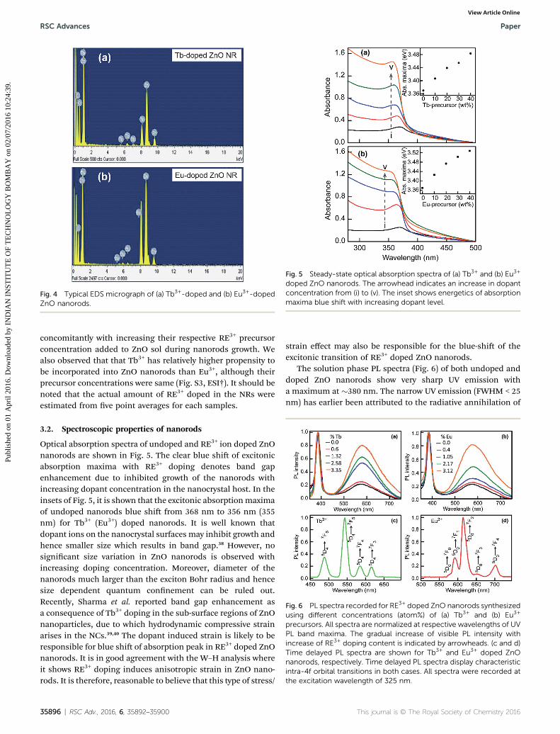
Fig. 4 Typical EDS micrograph of (a) Tb3+-doped and (b) Eu3+-dopedZnO nanorods.
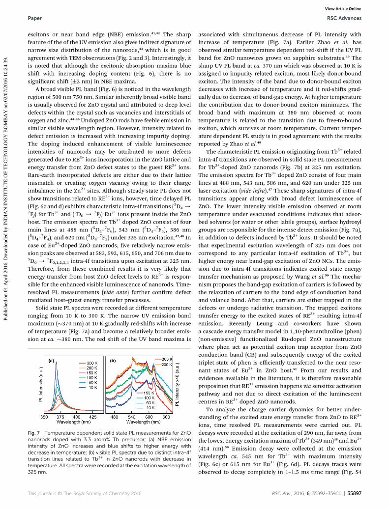
Fig. 5 Steady-state optical absorption spectra of (a) Tb3+ and (b) Eu3+
doped ZnO nanorods. The arrowhead indicates an increase in dopantconcentration from (i) to (v). The inset shows energetics of absorptionmaxima blue shift with increasing dopant level.
Fig. 6 PL spectra recorded for RE3+ doped ZnO nanorods synthesizedusing different concentrations (atom%) of (a) Tb3+ and (b) Eu3+
precursors. All spectra are normalized at respective wavelengths of UVPL band maxima. The gradual increase of visible PL intensity withincrease of RE3+ doping content is indicated by arrowheads. (c and d)Time delayed PL spectra are shown for Tb3+ and Eu3+ doped ZnOnanorods, respectively. Time delayed PL spectra display characteristicintra-4f orbital transitions in both cases. All spectra were recorded atthe excitation wavelength of 325 nm.
RSC Advances Paper
Publ
ishe
d on
01
Apr
il 20
16. D
ownl
oade
d by
IN
DIA
N I
NST
ITU
TE
OF
TE
CH
NO
LO
GY
BO
MB
AY
on
02/0
7/20
16 1
0:24
:39.
View Article Online
concomitantly with increasing their respective RE3+ precursorconcentration added to ZnO sol during nanorods growth. Wealso observed that that Tb3+ has relatively higher propensity tobe incorporated into ZnO nanorods than Eu3+, although theirprecursor concentrations were same (Fig. S3, ESI†). It should benoted that the actual amount of RE3+ doped in the NRs wereestimated from ve point averages for each samples.
3.2. Spectroscopic properties of nanorods
Optical absorption spectra of undoped and RE3+ ion doped ZnOnanorods are shown in Fig. 5. The clear blue shi of excitonicabsorption maxima with RE3+ doping denotes band gapenhancement due to inhibited growth of the nanorods withincreasing dopant concentration in the nanocrystal host. In theinsets of Fig. 5, it is shown that the excitonic absorptionmaximaof undoped nanorods blue shi from 368 nm to 356 nm (355nm) for Tb3+ (Eu3+) doped nanorods. It is well known thatdopant ions on the nanocrystal surfaces may inhibit growth andhence smaller size which results in band gap.38 However, nosignicant size variation in ZnO nanorods is observed withincreasing doping concentration. Moreover, diameter of thenanorods much larger than the exciton Bohr radius and hencesize dependent quantum connement can be ruled out.Recently, Sharma et al. reported band gap enhancement asa consequence of Tb3+ doping in the sub-surface regions of ZnOnanoparticles, due to which hydrodynamic compressive strainarises in the NCs.39,40 The dopant induced strain is likely to beresponsible for blue shi of absorption peak in RE3+ doped ZnOnanorods. It is in good agreement with the W–H analysis whereit shows RE3+ doping induces anisotropic strain in ZnO nano-rods. It is therefore, reasonable to believe that this type of stress/
35896 | RSC Adv., 2016, 6, 35892–35900
strain effect may also be responsible for the blue-shi of theexcitonic transition of RE3+ doped ZnO nanorods.
The solution phase PL spectra (Fig. 6) of both undoped anddoped ZnO nanorods show very sharp UV emission witha maximum at �380 nm. The narrow UV emission (FWHM < 25nm) has earlier been attributed to the radiative annihilation of
This journal is © The Royal Society of Chemistry 2016
Paper RSC Advances
Publ
ishe
d on
01
Apr
il 20
16. D
ownl
oade
d by
IN
DIA
N I
NST
ITU
TE
OF
TE
CH
NO
LO
GY
BO
MB
AY
on
02/0
7/20
16 1
0:24
:39.
View Article Online
excitons or near band edge (NBE) emission.41,42 The sharpfeature of the of the UV emission also gives indirect signature ofnarrow size distribution of the nanorods,43 which is in goodagreement with TEM observations (Fig. 2 and 3). Interestingly, itis noted that although the excitonic absorption maxima blueshi with increasing doping content (Fig. 6), there is nosignicant shi (�2 nm) in NBE maxima.
A broad visible PL band (Fig. 6) is noticed in the wavelengthregion of 500 nm 750 nm. Similar inherently broad visible bandis usually observed for ZnO crystal and attributed to deep leveldefects within the crystal such as vacancies and interstitials ofoxygen and zinc.44–46 Undoped ZnO rods have feeble emission insimilar visible wavelength region. However, intensity related todefect emission is increased with increasing impurity doping.The doping induced enhancement of visible luminescenceintensities of nanorods may be attributed to more defectsgenerated due to RE3+ ions incorporation in the ZnO lattice andenergy transfer from ZnO defect states to the guest RE3+ ions.Rare-earth incorporated defects are either due to their latticemismatch or creating oxygen vacancy owing to their chargeimbalance in the Zn2+ sites. Although steady-state PL does notshow transitions related to RE3+ ions, however, time delayed PL(Fig. 6c and d) exhibits characteristic intra-4f transitions (5D4/7Fj) for Tb
3+ and (5D0 /7Fj) Eu
3+ ions present inside the ZnOhost. The emission spectra for Tb3+ doped ZnO consist of fourmain lines at 488 nm (5D4–
7F6), 543 nm (5D4–7F5), 586 nm
(5D4–7F4), and 620 nm (5D4–
7F3) under 325 nm excitation.47,48 Incase of Eu3+-doped ZnO nanorods, ve relatively narrow emis-sion peaks are observed at 583, 592, 615, 650, and 706 nm due to5D0 /
7F0,1,2,3,4 intra-4f transitions upon excitation at 325 nm.Therefore, from these combined results it is very likely thatenergy transfer from host ZnO defect levels to RE3+ is respon-sible for the enhanced visible luminescence of nanorods. Time-resolved PL measurements (vide ante) further conrm defectmediated host–guest energy transfer processes.
Solid state PL spectra were recorded at different temperatureranging from 10 K to 300 K. The narrow UV emission bandmaximum (�370 nm) at 10 K gradually red-shis with increaseof temperature (Fig. 7a) and become a relatively broader emis-sion at ca. �380 nm. The red shi of the UV band maxima is
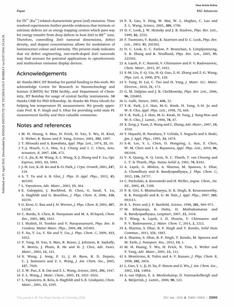
Fig. 7 Temperature dependent solid state PL measurements for ZnOnanorods doped with 3.3 atom% Tb precursor; (a) NBE emissionintensity of ZnO increases and blue shifts to higher energy withdecrease in temperature; (b) visible PL spectra due to distinct intra-4ftransition lines related to Tb3+ in ZnO nanorods with decrease intemperature. All spectra were recorded at the excitation wavelength of325 nm.
This journal is © The Royal Society of Chemistry 2016
associated with simultaneous decrease of PL intensity withincrease of temperature (Fig. 7a). Earlier Zhao et al. hasobserved similar temperature dependent red-shi if the UV PLband for ZnO nanowires grown on sapphire substrates.49 Thesharp UV PL band at ca. 370 nm which was observed at 10 K isassigned to impurity related exciton, most likely donor-boundexciton. The intensity of the band due to donor-bound excitondecreases with increase of temperature and it red-shis grad-ually due to decrease of band-gap energy. At higher temperaturethe contribution due to donor-bound exciton minimizes. Thebroad band with maximum at 380 nm observed at roomtemperature is related to the transition due to free-to-boundexciton, which survives at room temperature. Current temper-ature dependent PL study is in good agreement with the resultsreported by Zhao et al.49
The characteristic PL emission originating from Tb3+ relatedintra-4f transitions are observed in solid state PL measurementfor Tb3+-doped ZnO nanorods (Fig. 7b) at 325 nm excitation.The emission spectra for Tb3+ doped ZnO consist of four mainlines at 488 nm, 543 nm, 586 nm, and 620 nm under 325 nmlaser excitation (vide infra).47 These sharp signatures of intra-4ftransitions appear along with broad defect luminescence ofZnO. The lower intensity visible emission observed at roomtemperature under evacuated conditions indicates that adsor-bed solvents (or water or other labile groups), surface hydroxylgroups are responsible for the intense detect emission (Fig. 7a),in addition to defects induced by Tb3+ ions. It should be notedthat experimental excitation wavelength of 325 nm does notcorrespond to any particular intra-4f excitation of Tb3+, buthigher energy near band-gap excitation of ZnO NCs. The emis-sion due to intra-4f transitions indicates excited state energytransfer mechanism as proposed by Wang et al.50 The mecha-nism proposes the band-gap excitation of carriers is followed bythe relaxation of carriers to the band edge of conduction bandand valance band. Aer that, carriers are either trapped in thedefects or undergo radiative transition. The trapped excitonstransfer energy to the excited states of RE3+ resulting intra-4femission. Recently Leung and co-workers have showna cascade energy transfer model in 1,10-phenanthroline (phen)(non-emissive) functionalized Eu-doped ZnO nanostructurewhere phen act as potential exciton trap acceptor from ZnOconduction band (CB) and subsequently energy of the excitedtriplet state of phen is efficiently transferred to the near reso-nant states of Eu3+ in ZnO host.51 From our results andevidences available in the literature, it is therefore reasonableproposition that RE3+ emission happens via sensitize activationpathway and not due to direct excitation of the luminescentcentres in RE3+ doped ZnO nanorods.
To analyze the charge carrier dynamics for better under-standing of the excited state energy transfer from ZnO to RE3+
ions, time resolved PL measurements were carried out. PLdecays were recorded at the excitation of 290 nm, far away fromthe lowest energy excitation maxima of Tb3+ (349 nm)48 and Eu3+
(414 nm).50 Emission decay were collected at the emissionwavelength ca. 545 nm for Tb3+ with maximum intensity(Fig. 6c) or 615 nm for Eu3+ (Fig. 6d). PL decays traces wereobserved to decay completely in 1–1.5 ms time range (Fig. S4
RSC Adv., 2016, 6, 35892–35900 | 35897
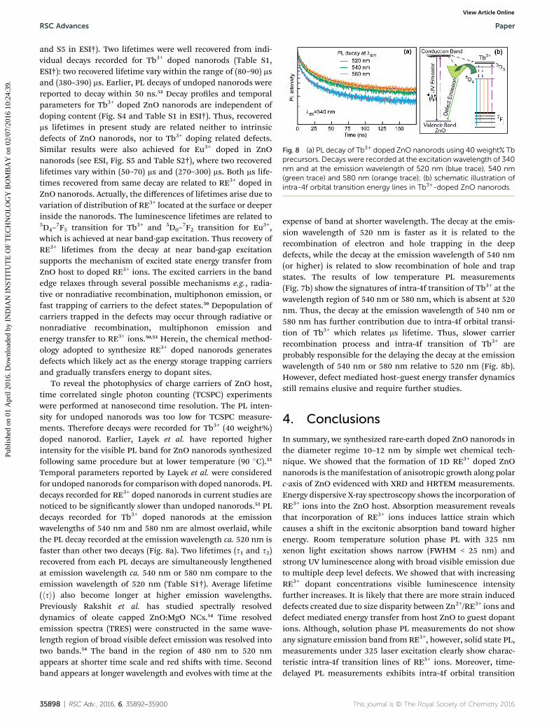
Fig. 8 (a) PL decay of Tb3+ doped ZnO nanorods using 40 weight% Tbprecursors. Decays were recorded at the excitation wavelength of 340nm and at the emission wavelength of 520 nm (blue trace), 540 nm(green trace) and 580 nm (orange trace); (b) schematic illustration ofintra-4f orbital transition energy lines in Tb3+-doped ZnO nanorods.
RSC Advances Paper
Publ
ishe
d on
01
Apr
il 20
16. D
ownl
oade
d by
IN
DIA
N I
NST
ITU
TE
OF
TE
CH
NO
LO
GY
BO
MB
AY
on
02/0
7/20
16 1
0:24
:39.
View Article Online
and S5 in ESI†). Two lifetimes were well recovered from indi-vidual decays recorded for Tb3+ doped nanorods (Table S1,ESI†): two recovered lifetime vary within the range of (80–90) msand (380–390) ms. Earlier, PL decays of undoped nanorods werereported to decay within 50 ns.52 Decay proles and temporalparameters for Tb3+ doped ZnO nanorods are independent ofdoping content (Fig. S4 and Table S1 in ESI†). Thus, recoveredms lifetimes in present study are related neither to intrinsicdefects of ZnO nanorods, nor to Tb3+ doping related defects.Similar results were also achieved for Eu3+ doped in ZnOnanorods (see ESI, Fig. S5 and Table S2†), where two recoveredlifetimes vary within (50–70) ms and (270–300) ms. Both ms life-times recovered from same decay are related to RE3+ doped inZnO nanorods. Actually, the differences of lifetimes arise due tovariation of distribution of RE3+ located at the surface or deeperinside the nanorods. The luminescence lifetimes are related to5D4–
7F5 transition for Tb3+ and 5D0–7F2 transition for Eu3+,
which is achieved at near band-gap excitation. Thus recovery ofRE3+ lifetimes from the decay at near band-gap excitationsupports the mechanism of excited state energy transfer fromZnO host to doped RE3+ ions. The excited carriers in the bandedge relaxes through several possible mechanisms e.g., radia-tive or nonradiative recombination, multiphonon emission, orfast trapping of carriers to the defect states.50 Depopulation ofcarriers trapped in the defects may occur through radiative ornonradiative recombination, multiphonon emission andenergy transfer to RE3+ ions.50,53 Herein, the chemical method-ology adopted to synthesize RE3+ doped nanorods generatesdefects which likely act as the energy storage trapping carriersand gradually transfers energy to dopant sites.
To reveal the photophysics of charge carriers of ZnO host,time correlated single photon counting (TCSPC) experimentswere performed at nanosecond time resolution. The PL inten-sity for undoped nanorods was too low for TCSPC measure-ments. Therefore decays were recorded for Tb3+ (40 weight%)doped nanorod. Earlier, Layek et al. have reported higherintensity for the visible PL band for ZnO nanorods synthesizedfollowing same procedure but at lower temperature (90 �C).52
Temporal parameters reported by Layek et al. were consideredfor undoped nanorods for comparison with doped nanorods. PLdecays recorded for RE3+ doped nanorods in current studies arenoticed to be signicantly slower than undoped nanorods.52 PLdecays recorded for Tb3+ doped nanorods at the emissionwavelengths of 540 nm and 580 nm are almost overlaid, whilethe PL decay recorded at the emission wavelength ca. 520 nm isfaster than other two decays (Fig. 8a). Two lifetimes (s1 and s2)recovered from each PL decays are simultaneously lengthenedat emission wavelength ca. 540 nm or 580 nm compare to theemission wavelength of 520 nm (Table S1†). Average lifetime(hsi) also become longer at higher emission wavelengths.Previously Rakshit et al. has studied spectrally resolveddynamics of oleate capped ZnO:MgO NCs.54 Time resolvedemission spectra (TRES) were constructed in the same wave-length region of broad visible defect emission was resolved intotwo bands.54 The band in the region of 480 nm to 520 nmappears at shorter time scale and red shis with time. Secondband appears at longer wavelength and evolves with time at the
35898 | RSC Adv., 2016, 6, 35892–35900
expense of band at shorter wavelength. The decay at the emis-sion wavelength of 520 nm is faster as it is related to therecombination of electron and hole trapping in the deepdefects, while the decay at the emission wavelength of 540 nm(or higher) is related to slow recombination of hole and trapstates. The results of low temperature PL measurements(Fig. 7b) show the signatures of intra-4f transition of Tb3+ at thewavelength region of 540 nm or 580 nm, which is absent at 520nm. Thus, the decay at the emission wavelength of 540 nm or580 nm has further contribution due to intra-4f orbital transi-tion of Tb3+ which relates ms lifetime. Thus, slower carrierrecombination process and intra-4f transition of Tb3+ areprobably responsible for the delaying the decay at the emissionwavelength of 540 nm or 580 nm relative to 520 nm (Fig. 8b).However, defect mediated host–guest energy transfer dynamicsstill remains elusive and require further studies.
4. Conclusions
In summary, we synthesized rare-earth doped ZnO nanorods inthe diameter regime 10–12 nm by simple wet chemical tech-nique. We showed that the formation of 1D RE3+ doped ZnOnanorods is themanifestation of anisotropic growth along polarc-axis of ZnO evidenced with XRD and HRTEM measurements.Energy dispersive X-ray spectroscopy shows the incorporation ofRE3+ ions into the ZnO host. Absorption measurement revealsthat incorporation of RE3+ ions induces lattice strain whichcauses a shi in the excitonic absorption band toward higherenergy. Room temperature solution phase PL with 325 nmxenon light excitation shows narrow (FWHM < 25 nm) andstrong UV luminescence along with broad visible emission dueto multiple deep level defects. We showed that with increasingRE3+ dopant concentrations visible luminescence intensityfurther increases. It is likely that there are more strain induceddefects created due to size disparity between Zn2+/RE3+ ions anddefect mediated energy transfer from host ZnO to guest dopantions. Although, solution phase PL measurements do not showany signature emission band from RE3+, however, solid state PL,measurements under 325 laser excitation clearly show charac-teristic intra-4f transition lines of RE3+ ions. Moreover, time-delayed PL measurements exhibits intra-4f orbital transition
This journal is © The Royal Society of Chemistry 2016
Paper RSC Advances
Publ
ishe
d on
01
Apr
il 20
16. D
ownl
oade
d by
IN
DIA
N I
NST
ITU
TE
OF
TE
CH
NO
LO
GY
BO
MB
AY
on
02/0
7/20
16 1
0:24
:39.
View Article Online
for Tb3+ (Eu3+) related characteristic green (red) emission. Timeresolved experiments further provide evidences that intrinsic orextrinsic defects act as energy trapping centres which pave wayfor energy transfer from deep defects in host ZnO to RE3+ ions.Therefore, controlling ZnO nanorod dimensions, defectdensity, and dopant concentrations allows for modulation ofluminescence colour and intensity. The present study indicatesthat via defect engineering, rare-earth-doped ZnO nanorodsmay nd avenues for potential applications in optoelectronicand multicolour emission display devices.
Acknowledgements
AC thanks IRCC IIT Bombay for partial funding to this work. Weacknowledge Centre for Research in Nanotechnology andScience (CRNTS) for TEM facility, and Department of Chem-istry, IIT Bombay for usage of central facility instruments. SBthanks CSIR for PhD fellowship. AL thanks Mr Pintu Ghosh forhelping low temperature PL measurement. We greatly appre-ciate Prof. B. P. Singh and S. Dhar for providing solid state PLmeasurement facility and their valuable comments.
Notes and references
1 M. H. Huang, S. Mao, H. Feick, H. Yan, Y. Wu, H. Kind,E. Weber, R. Russo and P. Yang, Science, 2001, 292, 1897.
2 T. Shiosaki and A. Kawabata, Appl. Phys. Lett., 1974, 25, 10.3 T.-J. Hsueh, C.-L. Hsu, S.-J. Chang and I. C. Chen, Sens.Actuators, B, 2007, 126, 473.
4 C.-L. Jia, K.-M. Wang, X.-L. Wang, X.-J. Zhang and F. Lu, Opt.Express, 2005, 13, 5093.
5 J.-H. Lee, K.-H. Ko and B.-O. Park, J. Cryst. Growth, 2003, 247,119.
6 A. T. Yu and A. B. Glot, J. Phys. D: Appl. Phys., 2012, 45,465305.
7 L. Vayssieres, Adv. Mater., 2003, 15, 464.8 E. Galoppini, J. Rochford, H. Chen, G. Saraf, Y. Lu,A. Hagfeldt and G. Boschloo, J. Phys. Chem. B, 2006, 110,16159.
9 G. Kron, U. Rau and J. H. Werner, J. Phys. Chem. B, 2003, 107,13258.
10 C. Burda, X. Chen, R. Narayanan and M. A. El-Sayed, Chem.Rev., 2005, 105, 1025.
11 I. Shalish, H. Temkin and V. Narayanamurti, Phys. Rev. B:Condens. Matter Mater. Phys., 2004, 69, 245401.
12 F. Xu, Y. Lu, Y. Xie and Y. Liu, J. Phys. Chem. C, 2009, 113,1052.
13 P. Yang, H. Yan, S. Mao, R. Russo, J. Johnson, R. Saykally,N. Morris, J. Pham, R. He and H. J. Choi, Adv. Funct.Mater., 2002, 12, 323.
14 X. Wang, J. Song, P. Li, J. H. Ryou, R. D. Dupuis,C. J. Summers and Z. L. Wang, J. Am. Chem. Soc., 2005,127, 7920.
15 Z. W. Pan, Z. R. Dai and Z. L. Wang, Science, 2001, 291, 1947.16 Z. L. Wang, J. Mater. Chem., 2005, 15, 1021–1024.17 L. Vayssieres, K. Keis, A. Hagfeldt and S.-E. Lindquist, Chem.
Mater., 2001, 13, 4395.
This journal is © The Royal Society of Chemistry 2016
18 P. X. Gao, Y. Ding, W. Mai, W. L. Hughes, C. Lao andZ. L. Wang, Science, 2005, 309, 1700.
19 D. C. Look, J. W. Hemsky and J. R. Sizelove, Phys. Rev. Lett.,1999, 82, 2552.
20 F. Tuomisto, V. Ranki, K. Saarinen and D. C. Look, Phys. Rev.Lett., 2003, 91, 205502.
21 D. C. Look, G. C. Farlow, P. Reunchan, S. Limpijumnong,S. B. Zhang and K. Nordlund, Phys. Rev. Lett., 2005, 95,225502.
22 A. Layek, P. C. Stanish, V. Chirmanov and P. V. Radovanovic,Chem. Mater., 2015, 27, 1021.
23 S.-M. Liu, F.-Q. Liu, H.-Q. Guo, Z.-H. Zhang and Z.-G. Wang,Phys. Lett. A, 2000, 271, 128.
24 Y. Yang, H. Lai, C. Tao and H. Yang, J. Mater. Sci.: Mater.Electron., 2010, 21, 173.
25 G. M. Dalpian and J. R. Chelikowsky, Phys. Rev. Lett., 2006,96, 226802.
26 G. Galli, Nature, 2005, 436, 32.27 Y.-K. Park, J.-I. Han, M.-G. Kwak, H. Yang, S.-H. Ju and
W.-S. Cho, Appl. Phys. Lett., 1998, 72, 668.28 Y.-K. Park, J.-I. Han, M.-G. Kwak, H. Yang, J. Sung-Hoo and
W.-S. Cho, J. Lumin., 1998, 78, 87.29 X. Zeng, J. Yuan, Z. Wang and L. Zhang, Adv. Mater., 2007, 19,
4510.30 Y. Hayashi, H. Narahara, T. Uchida, T. Noguchi and S. Ibuki,
Jpn. J. Appl. Phys., 1995, 34, 1878.31 S.-K. Lee, S. L. Chen, D. Hongxing, L. Sun, Z. Chen,
W. M. Chen and I. A. Buyanova, Appl. Phys. Lett., 2010, 96,083104.
32 V. X. Quang, N. Q. Liem, N. C. Thanh, T. van Chuong andL. T. le Thanh, Phys. Status Solidi A, 1983, 78, K161.
33 A. Layek, G. Mishra, A. Sharma, M. Spasova, S. Dhar,A. Chowdhury and R. Bandyopadhyaya, J. Phys. Chem. C,2012, 116, 24757.
34 C. Pacholski, A. Kornowski and H. Weller, Angew. Chem., Int.Ed., 2002, 41, 1188.
35 P. K. Giri, S. Bhattacharyya, D. K. Singh, R. Kesavamoorthy,B. K. Panigrahi and K. G. M. Nair, J. Appl. Phys., 2007, 102,093515.
36 R. L. Penn and J. F. Baneld, Science, 1998, 281, 969–971.37 M. Ethayaraja, K. Dutta, D. Muthukumaran and
R. Bandyopadhyaya, Langmuir, 2007, 23, 3418.38 T. Wang, A. Layek, I. D. Hosein, V. Chirmanov and
P. V. Radovanovic, J. Mater. Chem. C, 2014, 2, 3212.39 A. Sharma, S. Dhar, B. P. Singh and T. Kundu, Solid State
Commun., 2011, 151, 1885.40 A. Sharma, S. Dhar, B. P. Singh, T. Kundu, M. Spasova and
M. Farle, J. Nanopart. Res., 2012, 14, 1.41 M. H. Huang, Y. Wu, H. Feick, N. Tran, E. Weber and
P. Yang, Adv. Mater., 2001, 13, 113.42 S. Monticone, R. Tufeu and A. V. Kanaev, J. Phys. Chem. B,
1998, 102, 2854.43 L. Guo, Y. L. Ji, H. Xu, P. Simon and Z. Wu, J. Am. Chem. Soc.,
2002, 124, 14864.44 A. van Dijken, E. A. Meulenkamp, D. Vanmaekelbergh and
A. Meijerink, J. Lumin., 2000, 90, 123.
RSC Adv., 2016, 6, 35892–35900 | 35899
RSC Advances Paper
Publ
ishe
d on
01
Apr
il 20
16. D
ownl
oade
d by
IN
DIA
N I
NST
ITU
TE
OF
TE
CH
NO
LO
GY
BO
MB
AY
on
02/0
7/20
16 1
0:24
:39.
View Article Online
45 A. Layek, S. De, R. Thorat and A. Chowdhury, J. Phys. Chem.Lett., 2011, 2, 1241.
46 B. Panigrahy, M. Aslam, D. S. Misra, M. Ghosh andD. Bahadur, Adv. Funct. Mater., 2010, 20, 1161.
47 S. Ji, L. Yin, G. Liu, L. Zhang and C. Ye, J. Phys. Chem. C, 2009,113, 16439.
48 L. Yang, Y. Li, Y. Xiao, C. Ye and L. Zhang, Chem. Lett., 2005,34, 828.
49 Q. X. Zhao, M. Willander, R. E. Morjan, Q.-H. Hu andE. E. B. Campbell, Appl. Phys. Lett., 2003, 83, 165.
35900 | RSC Adv., 2016, 6, 35892–35900
50 D.Wang, G. Xing, M. Gao, L. Yang, J. Yang and T. Wu, J. Phys.Chem. C, 2011, 115, 22729.
51 J. S. Kang, Y. K. Jeong, J. G. Kang, L. Zhao, Y. Sohn,D. Pradhan and K. T. Leung, J. Phys. Chem. C, 2015, 119,2142.
52 A. Layek, B. Manna and A. Chowdhury, Chem. Phys. Lett.,2012, 539–540, 133.
53 M. Zhong, G. Shan, Y. Li, G. Wang and Y. Liu, Mater. Chem.Phys., 2007, 106, 305.
54 S. Rakshit and S. Vasudevan, J. Phys. Chem. C, 2008, 112,4531.
This journal is © The Royal Society of Chemistry 2016
Related Documents


![Optical and structural properties of Si-doped ZnO thin films...Si-doped ZnO nanocomposites [8–10] and nanorods [11]. In the present work we examine Si-doped ZnO thin films pro-](https://static.cupdf.com/doc/110x72/610af404b2c50b3ec432d369/optical-and-structural-properties-of-si-doped-zno-thin-films-si-doped-zno-nanocomposites.jpg)
