i Synthesis, Integration, and Characterization of Functional Inorganic Nanomaterials by Huanan Duan A Dissertation Submitted to the Faculty of the WORCESTER POLYTECHNIC INSTITUTE in partial fulfillment of the requirements for the Degree of Doctor of Philosophy in Materials Science and Engineering _______________ May 2009 APPROVED: _______________________________________ Dr. Jianyu Liang, Advisor Assistant Professor of Mechanical Engineering _______________________________________ Dr. Richard D. Sisson, Jr., George F. Fuller Professor, Director of Manufacturing and Materials Engineering

Welcome message from author
This document is posted to help you gain knowledge. Please leave a comment to let me know what you think about it! Share it to your friends and learn new things together.
Transcript

i
Synthesis, Integration, and Characterization of Functional Inorganic
Nanomaterials
by
Huanan Duan
A Dissertation
Submitted to the Faculty
of the
WORCESTER POLYTECHNIC INSTITUTE
in partial fulfillment of the requirements for the
Degree of Doctor of Philosophy
in
Materials Science and Engineering
_______________
May 2009
APPROVED:
_______________________________________
Dr. Jianyu Liang, Advisor
Assistant Professor of Mechanical Engineering
_______________________________________
Dr. Richard D. Sisson, Jr., George F. Fuller Professor, Director of Manufacturing and Materials Engineering

ii
ABSTRACT
In the past decade nanomaterials have attracted the interest of scientists and engineers all
over the world due to their unique properties. Through their devoted experimental efforts,
limited advances have been made on the synthesis of nanomaterials, the integration of
nanomaterials into the structures of larger scales, and the property study of nanomaterials to
explore possible applications. Despite the huge amount of money, resources, and effort
invested in nanomaterials, several challenges still remain as obstacles on the way towards the
successful large scale use of nanomaterials to benefit human life and society. For example,
the need for low-cost, robust, and highly productive manufacturing methods and the demand
for efficient integration of nanomaterials with materials and devices of larger length scales
are still left unmet.
The objective of this work was to utilize cost-efficient nanofabrication methods such as
template-assisted fabrication, electrodeposition, and chemical vapor deposition to fabricate
nanomaterials, integrate nanomaterials with larger structures to form a hierarchical composite,
and explore the application of unique nanostructured electrode in lithium-ion batteries. Thus
the thesis consists of three main parts: (1) fabrication of one-dimensional inorganic
nanomaterials such as metal nanowires, metal nanorods, and carbon nanotubes with good
control over shape and dimension; (2) synthesis of hierarchical carbon nanofibers on carbon
microfibers and/or glass microfibers; and (3) development of nanostructured anodes to
improve high-rate capability of lithium-ion batteries by adapting nanorod arrays as miniature
current collectors.

iii
ACKNOWLEDGEMENTS
First and foremost, I would like to express my sincere appreciation and gratitude to my Ph.D.
advisor, Professor Jiangyu Liang who has been an exceptional research advisor and mentor
for the past four years. Her unbridled enthusiasm for research, dedication to work, support
and continual encouragements have been influencing me throughout this research and my
graduate experience.
I would also like to thank my committee members, Professor Richard D. Sisson, Jr.,
Professor Chrysanthe Demetry, Professor Germano S. Iannacchione, and Professor Zhenhai
Xia for their time and assistance throughout my graduate studies.
Thanks to the former and current members of Liang group, the various staff members in
the Materials Science and Engineering program, and colleagues in and outside of WPI who
made my years at WPI an enjoyable experience. Thanks to Rita L Shilansky who is the
“mom” of the graduate family. Thank you for providing the support while pursuing my
academic and personal goals.
I would also like to give thanks my friends at WPI including Wendi Liu, Shao-Wen Fan,
Xueying Huang, Shelley A Dougherty, Fan Wu, Songxiang Gu, and Shimin Li. Life in USA
would have never been the same. I would also like to mention “The drunken dream team”
(Basketball team), which left something unforgettable in my mind.
I would like to express my love and gratitude for my parents, Fangsheng Duan and
Yongyuan Guo. I have the utmost appreciation for everything my parents have done for me
throughout my life. I would also like to thank my sister, Huayan Duan, who has continually
supported and encouraged me along the way. Thank you all for the love and understanding in
this long journey.
Finally, but most importantly, I would like to thank my wife, Jing Zhong. Words can not
describe my love and appreciation for her. I feel truly blessed to have found someone with
whom I can share the rest of my life. I look forward to the future knowing that Jing will be by
my side.

iv
TABLE OF CONTENTS
ABSTRACT...............................................................................................................................ii
ACKNOWLEDGEMENTS..................................................................................................... iii
TABLE OF CONTENTS..........................................................................................................iv
CHAPTER I: INTRODUCTION...............................................................................................1 Research Objectives............................................................................................................2
Research Plan......................................................................................................................3
Thesis Organization ............................................................................................................4
CHAPTER II LITERATURE REVIEW ...................................................................................6 2.1 Nanomaterials ...............................................................................................................6
2.2 Nanofabrication of 1-D nanomaterials..........................................................................7
2.2.1 Lithography based growth ..................................................................................8
2.2.2 Vapor phase growth...........................................................................................11
2.2.3 Solution based growth.......................................................................................13
2.2.4 Template-assisted synthesis ..............................................................................14 2.3 Integration of carbon nanomaterials to materials with larger dimension scale ..........16
2.4 Application of nanomaterials as anode material for Li ion batteries ..........................17
2.4.1 Nanostructured electrode for Li ion batteries ...................................................17
2.4.2 Anode materials based on “conversion reactions”............................................19 Reference ..........................................................................................................................22
CHAPTER III: PUBLICATIONS............................................................................................31 PAPER # 1: A GENERIC SYNTHETIC APPROACH TO FABRICATE Y-JUNCTION
METAL NANOWIRES BY AAO TEMPLATES-ASSISTED AC
ELECTRODEPOSITION.................................................................................................31
PAPER # 2: SYNTHETIC HIERARCHICAL NANOSTRUCUTRES: GROWTH OF
CARBON NANOFIBERS ON MICROFIBERS BY CHEMICAL VAPOR
DEPOSITION...................................................................................................................40
PAPER # 3: NOVEL GROWTH MORPHOLOGY OF CATHODICALLY
ELECTRODEPOSITED Fe3O4 THIN FILMS.................................................................52
PAPER # 4: STUDY OF Fe3O4-BASED Cu NANOSTRUCUTRED ELECTRODE FOR
Li-ION BATTERY ...........................................................................................................65

v
CHAPTER IV: RESEARCH CONCLUSIONS AND FUTURE WORK...............................80
APPENDIX A: AAO-ASSISTED FABRICATION OF 1 D NANOMATERIALS...............83 1. AAO template synthesis ...............................................................................................83
2. AAO-template assisted nanofabrication .......................................................................85
APPENDIX B: ELECTROCHEMICAL PREPARATION OF NANOSTRUCTURED TiO2
AS ANODE MATERIAL FOR Li ION BATTERIES............................................................93

1
CHAPTER I: INTRODUCTION
Now more than ever, nanostructured materials have attracted tremendous interest from
scientists and engineers all over the globe. Nanostructured materials exhibit peculiar and
interesting properties superior to their bulk counterparts and have the potential to
revolutionize many areas of research. As a result, extensive research efforts have been
dedicated to studying various aspects of nanomaterials through numerical simulations and
experiments.
Compared to well-developed disciplines, nanotechnology is in its infancy. Most of the
current experimental work of nanomaterials is concentrated on the synthesis of
nanostructures, the integration of nanomaterials into the structures of larger scales, and the
property study of novel devices incorporating nanomaterials. This thesis focuses on using
methods that are simple, cost-efficient, and easy to scale up to produce unique nanomaterials
and design new devices to contribute to these three aspects.
Among the various nanomaterials, one-dimensional (1-D) nanostructures are of
particular interest because of their potential applications in nanoscale electronic and
optoelectronic devices. In particular, the fabrication of desired 1-D nanomaterials is still a
major challenge for nanotechnologists. In the past decade, several major fabrication strategies
such as lithography-based methods [1], self-assembly [2,3], vapor phase growth [4,5],
solution based growth [5,6], template-assisted synthesis [5,6], and microcontact printing [6]
have been explored and are under extensive and intensive study. Yet the journey to seek an
easy, low-cost, precise, and highly productive preparation method continues.
After the preparation of nanomaterials, how to manipulate, transfer, and assemble them
into functional devices and effectively integrate them with materials and devices of larger
length scales remains another major obstacle. Scanning probe microscopy (SPM) techniques,
for instance, have been used to manipulate atoms on metal surfaces and to fabricate
nanopatterns on metal and semiconductor surfaces [1]. However, this process is extremely
time-consuming, not cost efficient, and yields low throughput. An alternative route, instead of
dealing with the as-prepared nanomaterials, is to directly grow nanostructures on larger scale

2
functional substrates to make a hierarchical structure. Then the manipulation of nanomaterials
can be realized by handling the larger scaled substrate.
Nanomaterials and nanotechnology have the potential to revolutionize many traditional
disciplines. They offer solutions to many critical, challenging, and long-existing problems.
For instance, nanomaterials are expected to significantly improve the rate capability of
lithium-ion (Li-ion) batteries. It is well accepted that the limitations in the rate capability of
Li-ion batteries are mainly caused by slow solid-state diffusion of lithium ions in the
electrode materials [7,8]. Nanostructured materials are considered as active candidates to
tackle this problem because of the potential advantages they offer, such as: (i) short lithium
ion transport length due to small particle sizes; (ii) fast surface reactions resulting from large
electrode/electrolyte interface area; (iii) good accommodation of structure strains imposed by
electrochemical reactions; and (iv) the possibility of operation in systems with low electronic
conductivity due to short path lengths for electron transport. Thus, integration of
nanomaterials might be the key to the development of the next generation of Li-ion batteries
with high energy density and high power/current density.
The advantages of nanomaterials render them a very promising future. The synthesis,
integration, and property study of nanomaterials constitute three crucial and interconnected
aspects for the advancement of this field. The goal of this project is to explore these
cutting-edge frontiers and contribute to the booming nanoscience and nanotechnology fields.
Research Objectives
The goals for this project include: (1) fabricating quality 1-D inorganic nanomaterials
such as metal nanowires (NWs), metal nanorods (NRs), and carbon nanotubes (CNTs) with
good control over the shape and dimension using an anodized aluminum oxide (AAO)
template-assisted fabrication approach; (2) exploring the possibility of integration of
nanomaterials to materials with larger dimension scale by synthesizing hierarchical structures
of carbon nanofibers (CNFs) and carbon microfibers (CMFs) or glass microfibers (GMFs)
and; (3) developing nanostructured electrodes that will improve high-rate capability of Li-ion
batteries by adapting nanorod arrays as miniature current collectors and obtaining a better
understanding of the role of how the nanorod current collector array affects the structure of
3
deposited active materials and the electrochemical performance of the as-prepared electrode.
In order to achieve these goals, the following technical objectives have been identified:
Objective 1. To synthesize and study the structures of the ordered metallic NW arrays and
CNT arrays using the AAO template assisted fabrication approach;
Objective 2. To synthesize and study the hierarchical structures of CNFs and CMFs or
GMFs;
Objective 3. To design and study the electrochemical properties of nanostructured electrodes
(in collaboration with Yardney Technical Products, Inc.).
Research Plan
The research plan for this project focuses primarily on using cost-efficient methods such
as electrodeposition and chemical vapor deposition (CVD) to study the synthesis, integration,
and electrochemical properties of nanomaterials. This corresponds to the technical objectives
and consists of three aspects: (1) synthesis of ordered metallic NW arrays and CNT arrays, (2)
synthesis of the hierarchical structures of CNFs and CMFs or GMFs, and (3) the design and
property study of nanostructured electrodes for Li-ion batteries.
The research plan is given in more detail in the following outline:
1. Synthesis of ordered metallic NW/NR arrays and CNT arrays
(1) A generic synthetic approach to fabricate Y-junction metal nanowires by AAO
templates (submitted to Electrochemistry Communication) and (2) AAO-assisted
Fabrication of metal NWs/NRs and CNTs (included in Appendix A).
Linear and Y-junction metal NWs and CNTs were fabricated by AAO assisted
electrodeposition and CVD, respectively. For metal NWs, different metal species such as
cobalt and copper and different synthesis conditions were studied. CNTs were fabricated
using catalyst-loaded AAO templates and catalyst-free AAO templates. A detailed
microstructure and morphology study was presented.
2. Integration of nanomaterials
Synthetic Hierarchical nanostructures: Growth of Carbon Nanofibers on Microfibers by
Chemical Vapor Deposition (submitted to Materials Science and Technology B)
4
CNFs were grown on the surface of CMFs and GMFs to fabricate hierarchical
structures. A detailed morphology study was presented and the effect of synthesis
conditions on the morphology of CNFs was discussed according to vapor-liquid-solid
growth mechanisms.
3. Electrochemical property study of nanostructured electrodes for Li ion batteries
(1) Novel growth morphology of cathodically electrodeposited Fe3O4 thin films
(submitted to Thin Solid Films)
Fe3O4 thin films with different morphologies were fabricated on planar copper
substrates by electrodeposition. The effect of synthesis parameters such as temperature,
deposition duration, and electrolyte concentration on the resultant morphology were
studied and discussed.
(2) Study of Fe3O4-based Cu Nanostructured Electrode for Li-ion Battery (published in
Journal of Power Sources) and (3) Electrochemical preparation of nanostructured TiO2 as
anode material for Li ion batteries (published in Proc. MRS 2008, Boston, MA,
1127-T01-02 and included in Appendix B)
Nanostructured electrodes were fabricated using copper NR arrays as miniature
current collectors. The active material of Fe3O4 and TiO2 were loaded by
electrodeposition. The electrochemical properties, namely charge/discharge capacity and
rate capability, were studied and compared to the electrodes using planar copper foils as
current collectors. The effect of the introduction of Cu NR arrays was discussed.
Thesis Organization
This thesis is divided into four chapters. This introductory chapter serves to familiarize
the reader with the motivations and goals that have driven this project. Chapter II: Literature
Review is a summary of relevant research which has been done in the aforementioned three
areas. Chapter III: Publications compiles the journal articles that have either been published
or submitted to peer-reviewed journals regarding the three aspects as outlined by the research
plan. This thesis closes with conclusions and recommendations for future work in Chapter IV.
Appendix A contains supporting information and some interesting experimental results of
metal NWs/NRs and CNTs which either lay the foundation of the AAO template-assisted

5
method or may lead to interesting future research work. Included in Appendix B is a
conference preceding paper detailing the fabrication of nanostrucutured TiO2 electrodes for
Li-ion batteries.
Reference
[1] Liu, G.; Xu, S.; Qian, Y. Acc. Chem. Res. 2000, 33, 457. [2] Cheng, J. Y.; Ross, C. A.; Smith, H. I.; Thomas, E. L. Adv. Mater. 2006, 18, 2505.
[3] Ariga, K.; Hill, J. P.; Lee, M. V.; Vinu, A.; Charvet, R.; Acharya, S. Sci. Technol. Adv.
Mater. 2008, 9, 014109.
[4] Weber, J.; Singhal, R.; Zekri, S.; Kumar, A. Inter. Mater. Rev. 2008, 53, 235.
[5] Wang, N.; Cai, Y.; Zhang, R.Q. Mater. Sci. Eng. R. 2008, 60, 1
[6] Gates, B. D.; Xu, Q.; Stewart, M.; Ryan, D.; Willson, C. G.; Whitesides, G. M. Chem. Rev.
2005, 105, 1171.
[7] Li, J.; Tang, Z.; Zhang, Z. Electrochem. Commun. 2005, 7, 62.
[8] Bruce, P. G. Chem. Commun. 1997, 19, 1817.
6
CHAPTER II LITERATURE REVIEW
In the -famous talk given at the annual meeting of the American Physical Society (APS) in
1959, “There’s Plenty of Room at the Bottom,” Nobel Prize laureate Richard Feynman
envisioned the promise of nanotechnology. Two decades later, the development of the
scanning tunneling microscope (STM) by IBM researchers gave scientists and engineers the
ability not only to image atoms but also to manipulate atoms and clusters with a precision of
a chemical bond. Also in the 1980s, Eric Drexler predicted a fantastic nanotechnology that
was beyond Feynman’s vision in several of his books. Later, fueled by breakthroughs such as
the discovery of carbon nanotubes, production of self-assembled monolayers, and creation of
quantum dots, together with advances in theory and modeling, nanotechnology took off.
With the fast advance in nanomaterials and nanotechnology, the debate over the future
and the real impact of nanotechnology on human life and society grew heated. On one hand,
nanotechnology has the potential to create many new materials and devices with wide-range
applications in various fields such as medicine, electronics, and energy production [1,2]. On
the other hand, nanotechnology raises many of the same issues as the introduction of a new
technology, including concerns about the toxicity, environmental impact [3], their potential
influence on global economics. Despite the ongoing debate, extensive research effort has
been and will continue being dedicated to studying the synthesis and various properties,
including thermal, electrical, mechanical, magnetic, and electrochemical properties, of
nanomaterials
2.1 Nanomaterials
So what are nanomaterials? The word nano, which means “dwarf” in Greek, is just a
fraction that indicated one billionth of a unit quantity. With major breakthroughs such as the
Noble prize winning discovery of bucky balls and carbon fullerene structures, the first
electron microscope images of carbon nanotubes, and the invention of inorganic fullerenes
and anisotropic nanostructures, nanomaterials have been inspiring a great amount of interest.
At present, realizing the importance of nanomaterials and heavy investment in
nanotechnology by governments and private sectors has become a global trend. State of the
7
art technology centers with excellent processing and characterization and device fabrication
facilities are being developed. The total amount of global funding invested in nanotechnology
has increased by a factor of 9.45 from 1997 to 2005 and the United States shows a similar
trend [4].
A large number of reviews and text books on the subjects of nanoscience and
nanotechnology have been published, endorsing it as the leading science and technology of
the 21st century [4-15]. The change of the dimension can lead to dramatic property change in
nanomaterials. For example, when within the length range of quantum confinement the
change in the dimensions in material result in changes of the total energy and the occupation
of the outermost energy level [4]. Thus engineering the nanostructured materials could realize
peculiar and fascinating physical and chemical properties superior to their bulk counterparts
[16]. For example, quantum dots show Coulomb blockade [17-19] and strongly
size-dependent optical and electrical properties [20], carbon nanotubes can have high
electrical conductivity and mechanical strength [21-23], and thin polymer films can have
glass-transition temperatures higher or lower than thick films [24,25].
Nanomaterials can be divided into zero-dimensional (nanocrystals, quantum dots), one-
dimensional (1-D, nanowires, nanotubes), and two-dimensional nanomaterials (nanofilms,
nanowalls). In particular, 1-D inorganic nanostructures which include nanotubes, nanorods,
nanowires, nanobelts, and nanoribbons have become the focus of intensive research because
they provide the ideal systems for investigating the dependence of electrical transport, optical
and mechanical properties on size and dimension [26-29]. These structures have a potential
broad impact on the research fields of medical sensing, drug delivery, microelectronics,
bio-microelectromechanics (MEMS), communications, energy storage, and computation
technology.
2.2 Nanofabrication of 1-D nanomaterials
Nanofabrication is the design and manufacture of materials with structural or chemical
restrictions on the nanometer scale along one or more of the dimensions. It, together with
characterization techniques, constitutes the cornerstone of the development of nanoscience

8
and nanotechnology. In the past couple of decades, developments in the semiconductor
industry have offered tremendous advancements in microelectronic devices and information
technologies. Microfabrication which makes devices on the micrometer scale by
photolithography-based techniques has grown into its mature stage and large-scale
commercial implementation of nanofabrication is sitting on the launch pad. According to the
International Technology Roadmap of Semiconductors (ITRS), if the industry is to keep its
pace on miniaturization by Moore’s law, the gate size of a field emission transistor will be
reduced to 25 nm by 2010 [30].
Strategies used to fabricate and assemble nanoscale materials and devices can be
classified as “top-down” and “bottom-up”. “Top-down” strategy begins with large
homogeneous objects and seeks to shrink them down to the nanoscale. The “bottom-up”
strategy uses the interactions between small components such as molecules or colloidal
particles to arrange themselves into more complex and discrete nanoscale structures. The
“bottom-up” synthesis method is considered a promising technique for addressing challenges
related to the traditional “top-down” methods. Both top-down and bottom-up methods have
been used to fabricate 1-D nanostructures. An exhaustive review of all the fabrication
techniques is beyond the scope of this chapter. Here, recent development of several
commonly used approaches, namely lithography based growth, vapor phase growth, solution
based growth, and template-assisted synthesis is briefly reviewed.
2.2.1 Lithography based growth
Lithography is a collective term for related series of processes including resist coating,
exposure, and development. The conventional lithographic approaches have achieved great
success and help the microelectronics industry maintain a continuous growth by doubling the
number of transistors on a single chip every 18 months [31]. Extensive literature exists on
lithography based processes [32-35].

9
Fig. 2.1 The schematic of lithography
Fig. 2.1 depicts a schematic process of conventional lithography. The work piece, an
unpatterned film or substrate, is first spin-coated with a uniform layer of resist dissolved in a
certain organic liquid solvent. The resist thickness is typically a few thousand angstroms to a
micron, depending on the spinning speed and the resist viscosity. A soft-bake of the resist is
necessary to remove the resist solvent and promote adhesion. Selected areas of the resist are
then exposed to a radiation source, often through a mask. Upon sufficient exposure, the
polymer chains in the resist are either broken (positive resist), or become cross-linked
(negative resist, poorer resolving power). The exposed resist often goes through a
post-exposure bake to promote homogeneity, before developed to form a positive or negative
image of the mask. By choosing the right developer, temperature and developing time, one
can obtain straight, round-off or undercut depth profiles in the resist.
Pattern transfer can be realized in two general processes: from the resist to an
unpatterned film by wet or dry etching; or post-deposition onto patterned resist by lift-off
and/or electrodeposition. Wet etching uses chemical or electrochemical processes to dissolve
the materials. In dry etching, physical processes such as ion milling and sputter etching use
ion bombardment to remove the unwanted materials; chemical processes such as plasma
etching use active species to react with surface material and form volatile products; a
combination of both processes, such as reactive ion etching, takes advantage of both
principles. At the end of the process, the remaining resist is stripped away.
The lithography resolution limit is ultimately determined by the radiation wavelength. To

10
satisfy the ever-increasing demand for fabricating features at length scales below 100 nm,
great efforts have been made to obtain a higher resolution. One strategy is to employ a
radiation source with shorter wavelengths than conventional ultra-violet photos such as
electron-beams (E-beam), extreme ultra-violet (EUV) light, focused ion beams, and X-rays. A
comparison of these nanolithography techniques is given in Table 2.1 [36]. Alternative
techniques such as near-field photolithography [37-42] are able to circumvent the diffraction
limit and achieve feature sizes as small as 50 nm [39]. Nevertheless, lithography-based
technologies suffer from limitations such as high capital and operating costs, low throughput,
restriction to fabrication on planar substrates, corrosive etchants, high-energy radiation, and
relatively high temperatures.
Table 2.1 Comparison of primary nanolithography techniques [36,43]
Features Technique Radiation
sources Dimension features Other features
Optical/
Photo lithography
UV light Resolution of 100 nm
and min. inter-level
alignment of 30 nm
Throughput of 1010
features s-1
E-Beam and direct
writing
Electron
beam
Resolution of 10 nm and
min. inter-level
alignment of 10 nm
Max. working area of 1 ×
1 μm2 and throughput of
104 features s-1
E-beam and etching Electron
beam
Resolution of 20 nm Max. working area of 750
× 750 μm2
X-ray lithography X-ray Resolution of 88 nm Max. working area of 5 ×
5 μm2
Focused ion beam
lithography
Ion beam Resolution of 30 nm and
min. inter-level
alignment of 10 nm
Throughput of 10-102
features s-1
EUV lithography EUV light Resolution of 30 nm and
min. inter-level
alignment of 10 nm
Max. working area of 26 ×
33 mm2 and throughput of
10 features s-1
11
2.2.2 Vapor phase growth
Vapor phase growth is a popular and extensively used mechanism for the synthesis of
1-D nanostructures. Two important mechanisms of vapor phase growth are vapor-liquid-solid
(VLS) and vapor-solid (VS) growth. In both mechanisms, control of the supersaturation level
determines the structural growth morphology.
Vapor-liquid-solid mechanism
In the past few years, the VLS mechanism has become widely used to generate 1-D
inorganic nanostructures such as oxides (ZnO, SnO2, ITO, MgO) [44-46], element
semiconductors (Si, Ge) [47,48], III-V semiconductors (GaN, GaAs, InAs, InP) [49-52],
II-VI semiconductors (ZnS, ZnSe, CdS, CdSe) [53-56], and recently CdS/Si coaxial
nanowires [57]. Briefly, 1-D growth is induced by the dissolution of gaseous reactants into
liquid droplets of catalyst material, followed by nucleation and growth of single crystalline
nanostructures. The primary steps in a typical VLS growth process are shown schematically
in Fig. 2.2. As the gaseous reactants dissolve into the metal catalysts, alloying occurs and the
metal liquid alloy forms at the eutectoid temperature. Nanowire nucleation begins once the
liquid droplet is supersaturated with the source element. Once the source element nanocrystal
nucleates at the liquid-solid interface, further condensation/dissolution of the source element
into the system will increase the amount of its precipitation from the alloy, leading to
nanowire growth. It is also determined that there is a linear relationship between the initial
catalyst particle size and the final nanowire diameter [47]. Gudiksen and Lieber demonstrated
this linear correlation by showing that GaP nanowires of selective diameter can be
synthesized by controlling the diameter of gold catalyst nanoparticles [58].
12
Fig. 2.2 Schematic illustration of vapor-liquid-solid nanowire growth mechanism including
three stages (I) alloying, (II) nucleation, and (III) axial growth [47].
Other VLS methods include pulsed laser deposition (PLD), chemical vapor deposition
(CVD), metal-organic chemical vapor deposition (MOCVD) and physical vapor deposition
(PVD). A brief comparison of these methods is given in Table 2.2.
Table 2.2 The comparison of some VLS methods
Method Description Examples
PLD Target material exposed to a laser beam
is vaporized and subsequently deposited
on a substrate. Usually used for catalyst
preparation, followed by VLS.
Single crystal Si and Ge
nanowires [59].
CVD A catalyst is heated to high temperatures
in a vacuum furnace, then chemical
precursors in gaseous form flow through
the tube reactor for a period of time.
Single-walled Carbon
nanotubes [60] and CNTs
[61].
MOCVD Similar to CVD except catalyst-free. ZnO nanowires grown on
a Si substrate [62,63].
PVD Nanostructures are deposited onto a
substrate by physical means.
CdS nanowires grown by
PVD of Cd S powders
[64].
Vapor-solid mechanism
13
Vapor-solid growth has also been used widely to produce nanostructures, including
oxide nanowires, whiskers of oxide, and metals with micrometer diameters [8,14]. In a
typical VS process, the vapor species is generated by evaporation, chemical reduction or
other gaseous reactions. These species are then transported and condensed onto the surface of
a solid substrate in a temperature zone lower than that of the source material. 1-D growth will
proceed without the need of a metal nanoparticle catalyst if the supersaturation in the solid
phase is kept at a specific low level to control the nucleation and the subsequent growth
process.
2.2.3 Solution based growth
Solution based growth (in aqueous or non-hydrolytic media) has been demonstrated as a
promising alternative approach for mass production of metal, semiconductor, and oxide
nanomaterials [8,14,15]. It mainly includes solution-liquid-solid (SLS), solvothermal, and
hydrothermal growth mechanisms. The primary advantage of solution based methods as
opposed to the vapor phase option is the ability to perform the growth at lower temperatures,
lower cost, and higher yield on a wide variety of substrates. In addition, this technique is able
to assemble nanocrystals with other functional materials to form hybrid nanostructures with
multiple functions and thus has great potential for applications in nanoelectronic and
biological systems.
Solution-liquid-solid methods
Buhro et al. [65-68] developed a low temperature SLS method similar to the VLS
process for the synthesis of crystalline nanowires of III-V semiconductors (InP, InAs, GaAs).
In this method, the precursors were delivered and reacted in the solution rather than the vapor
phase. As shown in Fig. 2.3, a typical procedure consists of a solution dispersion of small
liquid flux droplets and a solution phase that feeds the elements of the crystal phase into the
flux droplets. Pseudo-one-dimensional growth of the crystal phase from the flux droplets
occurs after the elements get supersaturated in the droplets. A metal (In, Sn, Bi) with a low
melting point is usually used as a catalyst, and the desired material is generated through the
decomposition of organometallic precursors dissolved in hydrocarbon solvents. The products

14
obtained are generally single-crystalline.
Fig. 2.3 Schematic illustration showing the growth of nanowire through the SLS mechanism
[65].
Solvothermal and hydrothermal methods
Solvothermal and hydrothermal methods are successfully employed as solution routes to
produce 1-D nanostructures such as Ge nanowires [69], CeS nanowires [70], ZnO nanowires
[71,72], α-MnO2 nanowires [73], and ZnS [74] and TiO nanostructures [75]. In these
processes, water or other organic solvents is mixed with metal precursors and crystal growth
regulating or templating agents, such as amines. This solution mixture is placed in an
autoclave and maintained at relatively high temperatures and pressures to carry out the crystal
growth and the assembly process.
2.2.4 Template-assisted synthesis
Template-assisted synthesis represents a convenient and versatile method to generate
1-D nanostructures. In this technique, a template with small holes within the host material
serves as a scaffold against which nanostructures with complimentary morphologies are
synthesized by filling the empty spaces. Broadly speaking, any material that can act as a
“structural director” can be employed as the template including nanowires [76,77], nanorods
[78], CNTs [79,80], DNA [81], and so-called “soft templates” such as some surfactants and
organic dopants [82,83]. In this project the template is defined as a “hard template” such as
an anodic aluminum oxide (AAO) membrane, nanochannel glass (NCG) [84,85], and porous

15
polymer membranes [86,87] in which the template contains nanoscale channels within the
host material.
AAO templates have attracted increasing attention as a template for nanofabrication due
to its simplicity and low cost [88,89]. It has been known for more than five decades that
alumina exhibits porous structure under certain electrochemical anodization conditions
[90,91]. A variety of electrolyte systems and a wide range of concentrations along with
different temperatures and anodization regimes have been studied. So far, the smallest pore
diameter reported is about 7 nm, using a sulfuric acid solution [92], while the largest, using a
phosphoric acid solution, is about 300nm [93]. Pore densities as high as 1011 pores cm-2 can
be obtained, and typical membrane thickness can range from 10 to 100 µm [88,94,95]. The
cell size of the hexagonal pattern was found be to proportional to the anodization voltage [96],
and the relationship between anodization voltage (V) and interpore distance (a) was
expressed in the following equation:
a = d + 2αV (1)
where d is the diameter of the pore and α is a constant with value around 1.2 nm V-1
[90,91]. Moreover, different mechanisms such as mechanical stress [97-99] and cellular
growth [100], have been proposed to describe the formation process of the self-ordered
hexagonal pore array. The methods for fabricating nanopore arrays of alumina are
well-established, and AAO membranes are commercially available (Whatman Anapore,
Anotech Separations).
After the synthesis of templates, the nanoscale channels can be filled by electrochemical
deposition, sol-gel, or a dip-coating method with a desired material. The 1-D nanostructures
are released from the templates by removal of the host AAO [88,101,102].
Electrochemical deposition
Electroplating is widely used to deposit metals. In the mid of 1990’s, the use of AAO
template assisted electrochemical deposition to prepare metal nanostructures was proposed
[88]. In this technique, the AAO template coated with a metallic conductive layer serves as a
cathode for electrodeposition. When a voltage is applied between the cathode and anode, the
cations in the electrolyte solutions are attracted to and get reduced near the cathode, which
results in nanowire growth in the pores of the template. The length of the nanowires depends
16
on the length of the nanochannels and the electrodeposition duration. The AAO
template-assisted fabrication approach has been proved to be a well-controlled approach to
fabricate ordered inorganic nanomaterial arrays with narrow diameter distribution. Diameter
of the nanomaterial arrays is limited by the pore size of the template which can be further
controlled by the anodization conditions and the wet etching steps after anodization.
Nanomaterials created through this technique include nanowires (Bi [103], Ni [104], Fe [105],
Co [106], NiFe [107]), tubes (carbon [108] and Cu [109]), dots (Co [110], Au [111], Fe [112]),
rods (Ga2O3-Al2O3 [113]), and superconducting materials (Sn [114]).
Sol-gel deposition
The sol-gel process involves the transition of a system of colloidal particles (the sol) into
a solid phase (the gel). First the hydrolysis of a solution of precursor molecules forms a
suspension of colloidal particles. Then the templates are immersedinto the solution and the
condensation of the colloidal particles within the nanochannels yields a new gel phase.
Finally post heat treatment turns the gel phase into solid nanostructures with good
crystallinity. The main advantages of sol-gel techniques include low temperature of
processing, versatility and easy chemical doping. Metal oxide nanowires (LiCoO2 [115],
LiMnO2 [116], LiNiO3 [117], TiO2 [118]), nanotubes (In2O3 and Ga2O3 [119]), and element
nanowires (Zr [120]) have been synthesized by this method.
Dip-coating deposition
The dip-coating process is similar to sol-gel deposition except that the template is put
into a precursor solution instead of the sol solution. Silver nanotubes are synthesized by
dipping the AAO template in AgNO3 solution followed by drying, thermal decomposition,
and subsequent dissolution of the AAO template [121].
2.3 Integration of carbon nanomaterials to materials with larger dimension scale
Carbon nanostructures have emerged as a new and attractive class of materials with
unique electrical, mechanical, physical, and chemical properties [122,123]. They are actively
studied for applications such as nanoelectronic devices [124-126], lithium ion battery
electrode material [127], field emission displays [128], storage materials for hydrogen and

17
other gases [129], and probe tips for atomic force microscopy (AFM) [130]. A lot of research
has focused on carbon nanotube (CNT) preparation techniques [131-135], theoretical
simulation to understand the physics of carbon nanostructures [136-139], and CNT
post-treatments such as purification, thermal annealing, and surface modification [140-142].
There is now a pressing need to integrate multicomponent nanoscale entities into
multifunctional systems and to connect these nanosystems to the micro/macro world.
Although a few innovative routes to the integration of CNTs into multidimensional and
multicomponent systems have recently been devised [143-145], the effective connection of
carbon nanostructures with materials and devices of larger length scales has been one of the
long-standing obstacles in nanotechnology and still remains a big challenge.
On the other hand, the multifunctional systems incorporating carbon-based hierarchical
structures are expected to provide advantageous properties for many applications. For
example, inspired by the remarkable hierarchical hairy structure of the feet of geckos and
many insects, researchers are working on creating new types of adhesives by mimicking this
structure using CNTs-based hierarchical structures [146-148]. Studies of the carbon-based
hierarchical structures as catalyst support for platinum particles for proton exchange
membrane fuel cells show that they may improve the platinum utilization by securing the
electronic route from platinum to the supporting electrode [149]. Thostenson demonstrated
that by covering individual carbon fibers (CFs) with a sheath of CNTs and embedding this
structure in a polymer matrix, the nanocomposite reinforcement resulted in local stiffening
near the fiber/matrix interface and improved the interfacial shear strength [150]. S. Lim et al
grew CNFs on activated CFs and used this composite to improve the efficiency of SOx or
NOx removal [151]. Similar carbon hierarchical structures were studied for drinking water
purification by selective chemosorption of chromate and heteropolymolybdate [152].
2.4 Application of nanomaterials as anode material for Li ion batteries
2.4.1 Nanostructured electrode for Li ion batteries
The Li-ion battery is one of the great successes of modern material electrochemistry
[153]. A conventional Li-ion battery consists of a negative electrode (generally graphite), a
18
positive electrode (generally the lithium metal oxide, LiCoO2), and a lithium ion conducting
electrolyte (for example a solution of LiPF6 in ethylene carbonate-diethylcarbonate).
Although such batteries are commercially successful because they have high specific energy,
energy density, and cycle life, they are reaching the limits in performance using the current
electrode and electrolyte materials. In addition, they suffer from several inherent challenges
such as the low discharge rate capability of graphite, limited volumetric and gravimetric
energy density, safety, life span limitation by Li-alloying agglomeration, and the capacity loss
due to the growth of passivation layers [154]. For applications in consumer electronics and
power sources in hybrid and electric vehicles, further breakthroughs in materials are highly
demanded.
It is now well established that limitations in the rate capability of Li-ion batteries are
mainly caused by slow solid-state diffusion of Li+ within the electrode materials [155,156].
Nanomaterials offer a promising alternative electrode material with remarkable properties.
The potential advantages of nanostructured electrodes for Li-ion batteries include: 1)
enabling new reactions not possible with bulk materials; 2) decreasing the particle size
resulting in a short lithium ion transport length; 3) increasing the electrode/electrolyte contact
area leading to a higher charge/discharge rate; 4) better accommodation of the strain of
structure change in active materials; and 5) short path lengths for electronic transport
permitting operation with low electronic conductivity of at high power [157,158]. The major
obstacles associated with nanoelectrodes are: 1) increased electrode/electrolyte interface area
leading to significant undesired electrode/electrolyte reactions, safety concerns and poor
calendar life; 2) inferior packing of nanoparticles resulting in lower volumetric energy
densities; and 3) the difficulty and expense in synthesizing the electrode [157].
Therefore there is a vigorous research effort in the use of nanomaterials to improve the
rate capabilities of solid-state electrodes. Carbon nanobeads and tin-filled carbon nanotubes
have been synthesized and studied for high-rate applications [159,160]. SnO2 nanofiber based
electrodes exhibited high capacities (>700 mAh g-1) at a very high discharge current (~10 C)
and still retained the ability to be discharged and recharged through as many as 800 cycles
[161-163]. Manganese oxide and titanium oxide nanocomposites with conducting carbon
19
showed good discharge-charge performances as cathode and anode materials under large
current density [164]. A honeycomb carbon anode containing an array of monodispersed
nanopores delivered 50 times the capacity of a thin-film control anode at high discharge rates
(10C) [165]. A nano/micro hierarchical Fe2O3/Ni wire electrode gave a high specific
charge/discharge capacity of 780 mAh g-1 with good cycle performance in a high
charge/discharge rate of 13 A g-1 [158]. Various nanoforms of TiO2, including nanocrystalline
anatase, amorphous TiO2 and TiO2 nanotubes, also received attention as high-rate Li-ion
anode materials and indeed demonstrated improved property at high current densities
[166-171].
2.4.2 Anode materials based on “conversion reactions”
A conventional Li-ion battery is based on the classical swing action of lithium ions
between positive electrodes (generally lithium metal oxide, LiCoO2) and negative electrodes
(generally graphite). Recently, some nanostructured compounds such as CoO, CuO, NiO,
Co3O4, and MnO, which are not suitable for the electrode in their usual macro-scale form, are
under intensive investigation. For these materials, the charge/discharge process involves a
novel reactivity mechanism, the so called “conversion reaction”, as summarized in Eq. 1:
MxNy + yz e- + yz Li+ ↔ x M0 + y LizN (2)
where M represents the metal cation and N, the non-metal anion. This mechanism differs
from the classical lithium insertion/deinsertion process or Li-alloying reactions. The full
electrochemical reduction of the compound MxNy involves multiple electrons per metal
cation and will lead to the formation of composite materials consisting of nanometer-scale
metallic clusters dispersed in an amorphous Li2O matrix [172]. The highest specific capacity
of the electrode material is attained by utilizing all the possible oxidation states of the
transition metal during the redox cycle. This type of reaction is proven not to be unique to
oxides and has been reported for sulphides, nitrides, fluorides, and phosphides [173]. One of
the main advantages of this conversion reaction is the superior capacity compared with
intercalation electrodes. Another attractive aspect is that such conversion reactions offer
numerous opportunities to “tune” the voltage and capacity of the cell due to the fact that the
cell potential is directly linked to the strength of the M-N bonding [154,157].
On the other hand, several issues have to be addressed to make full use of the materials

20
based on conversion reaction, as identified by N. G. Renganathan [154]: (1) poor kinetics that
result in a large polarization, and hence a poor energy efficiency, (2) poor capacity retention
upon cycling, (3) higher potentials, and hence a lower cell voltage, (4) irreversible capacity
loss on the first cycle, and (5) low coulombic efficiency. To address these problems, different
approaches have been explored such as studying different materials, coating the material
surfaces with conducting materials such as carbon, using thin-film material instead of bulk
material, and designing nanostructured electrodes. Some of the results are summarized in the
Table 2.3.
Table 2.3 Anode materials based on conversion reactions
Material Major results Reference
RuO2 Displays a 100% reversible conversion process involving
4e-. Coulombic efficiency of > 98%, a capacity of 1,110
mAh g-1 in the voltage range of 0.05-4.3 V and 99%
Coulombic efficiency, a capacity of 730 mAh g-1 at 0.8-4.3
V.
[174,175]
α-Fe2O3
nanoparticles
With nanometer-scale haematite particles (20 nm), 1 Li per
formular unit can be inserted in the corundum structure
without phase transformation, among which 0.6 Li is
reversibly inserted and the remaining 0.4 Li is irreversibly
inserted.
[176,177]
α-Fe2O3
nanoparticles
A capacity of 1000 mAh g-1 at a rate of 100 mA g-1 is
delivered with no overall fade after 50 cycles. A capacity of
700 mAh g-1 is obtained at a rate of 700 mA g-1. Electron
transport to and within the particles are the main factors
limiting the rate.
[178]
Fe2O3
nanoflake
A stable capacity of 680 + 20 mAh g-1 is obtained with no
noticeable capacity fading up to 80 cycles, when cycled in
the range of 0.005-3.0 V at 65 mA g-1 (0.1 C rate). A
coulombic efficiency of >98% is shown after the 15th cycle.
[179]
Nanoparticles A capacity of 700 mAh g-1 is demonstrated with 100% [172]
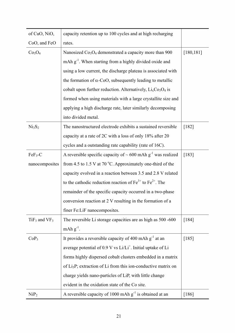
21
of CuO, NiO,
CoO, and FeO
capacity retention up to 100 cycles and at high recharging
rates.
Co3O4 Nanosized Co3O4 demonstrated a capacity more than 900
mAh g-1. When starting from a highly divided oxide and
using a low current, the discharge plateau is associated with
the formation of α-CoO, subsequently leading to metallic
cobalt upon further reduction. Alternatively, LixCo3O4 is
formed when using materials with a large crystallite size and
applying a high discharge rate, later similarly decomposing
into divided metal.
[180,181]
Ni3S2 The nanostructured electrode exhibits a sustained reversible
capacity at a rate of 2C with a loss of only 18% after 20
cycles and a outstanding rate capability (rate of 16C).
[182]
FeF3-C
nanocomposites
A reversible specific capacity of ~ 600 mAh g-1 was realized
from 4.5 to 1.5 V at 70 oC. Approximately one-third of the
capacity evolved in a reaction between 3.5 and 2.8 V related
to the cathodic reduction reaction of Fe3+ to Fe2+. The
remainder of the specific capacity occurred in a two-phase
conversion reaction at 2 V resulting in the formation of a
finer Fe:LiF nanocomposites.
[183]
TiF3 and VF3 The reversible Li storage capacities are as high as 500 -600
mAh g-1.
[184]
CoP3 It provides a reversible capacity of 400 mAh g-1 at an
average potential of 0.9 V vs Li/Li+. Initial uptake of Li
forms highly dispersed cobalt clusters embedded in a matrix
of Li3P; extraction of Li from this ion-conductive matrix on
charge yields nano-particles of LiP, with little change
evident in the oxidation state of the Co site.
[185]
NiP2 A reversible capacity of 1000 mAh g-1 is obtained at an [186]

22
average potential of 0.9 V vs Li+/Lio. It sustains 90% of its
capacity over 15 cycles and can deliver its full capacity at
0.5C.
Reference
[1] Alivisatos, P.; Barbara, P. F.; Castleman, A. W.; Chang, J.; Dixon, D. A.; Kline, M. L.;
McLendon, G. L.; Miller, J. S.; Ratner, M. A.; Rossky, P. J.; Stupp, S. I.; Thompson, M. I.
Adv. Mater. 1998, 10, 1297.
[2] Thiaville, A.; Miltat, J. Science 1999, 284, 1939.
[3] Buzea, C.; Pacheco, I.; Robbie, K. Biointerphases 2007, 2, MR17.
[4] Kuchibhatla, S.; Karakoti, A.S.; Bera, D.; Seal, S. Prog. Mater. Sci. 2007, 52, 699.
[5] Wang, Z. L.; Hui, C. Electron microscopy of nanotubes; Kluwer Academic Publishers:
Norwell, MA, 2003. [6] Baraton, M. I. Synthesis, functionalization and surface treatments of nanoparticles;
American Scientific Publishers: Valencia, CA, 2003.
[7] Yang, P. editor. The chemistry of nanostructured materials; World Scientific Publishing
Co. Pte. Ltd.: River Edge, NJ, 2003.
[8] Rao, C. N. R.; Deepak, F. L.; Gundiah, G.; Govindaraj, A. Prog Solid State Chem. 2003,
31, 5.
[9] Xia, Y. N.; Yang, P. D.; Sun, Y. G.; Wu, Y. Y.; Mayers, B. Adv. Mater. 2003, 15, 353.
[10] Suryanarayana, C. Adv. Eng. Mater. 2005, 7, 983.
[11] Gleiter, H. Acta Mater. 2000, 48, 1.
[12] Bera, D.; Deshpande, S.; Drake, C.; Seal, S. Int. Mater. Rev. 2007, 317, 29.
[13] Cavaleiro, A.; De Hosson, J. T. M. Nanostructured coatings; Springer Science New York,
NY, 2006.
[14] Weber, J.; Singhal, R.; Zekri, S.; Kumar, A. Inter. Mater. Rev. 2008, 53, 235.
[15] Wang, N.; Cai, Y.; Zhang, R. Q. Mater. Sci. Eng. R. 2008, 60, 1.
[16] Nalwa, H. S. Handbook of Nanostructured Materials and Nanotechnology; Academic
Press: New York, NY, 2000.
[17] Feldheim, D. L.; Keating, C. D. Chem. Soc. Rev. 1998, 27, 1.
[18] Klein, D. L.; Roth, R.; Lim, A. K. L.; Alivisatos, A. P.; McEuen, P. L. Nature 1997, 389,
699.

23
[19] Kran, J. M.; van Rutenbeek, J. M.; Fisun, V. V.; Yanson, I. K.; Jongh, L. J. Nature 1995,
375, 767.
[20] Alivisatos, A. P. Science 1996, 271, 933.
[21] Bockrath, M.; Cobden, D. H.; McEuen, P. L.; Chopra, N. G.; Zettl, A.; Thess, A.; Smalley,
R. E. Science 1997, 275, 1922.
[22] Venema, L. C.; Wildoer, J. W. G.; Janssen, J. W.; Tans, S. J.; Tuinstra, H. L. J. T.;
Kouwenhoven, L. P.; Dekker, C. Science 1999, 283, 52.
[23] Bockrath, M.; Liang, W.; Bozovic, D.; Hafner, J. H.; Lieber, C. M.; Tinkham, M.; Park, H.
Science 2001, 291, 283.
[24] Singh, L.; Ludovice, P. J.; Henderson, C. L. Thin Solid Films 2004, 449, 231.
[25] Torres, J. A.; Nealey, P. F.; de Pablo, J. J. Phys. Rev. Lett. 2000, 85, 3221.
[26] Wang, Z. L. Adv. Mater. 2000, 12, 1295.
[27] Hu, J.; Odom, T. W.; Lieber, C. M. Acc. Chem. Res. 1999, 32, 1295.
[28] Xia, Y. N.; Yang, P. D.; Sun, Y. G.; Wu, Y. Y.; Mayers, B.; Gates, B.; Yin, Y. D.; Kim, F.;
Yan, H. Q. Adv. Mater. 2003, 15, 353.
[29] Craighead, H. G. Science 2000, 290, 1532.
[30] International Technology Roadmap for Semiconductors web site. http://public.itrs.net.
[31] The National Technology Roadmap for Semiconductor Industry Association, 1999. [32] Sheats, J. R.; Smith, B.W. Microlithography Science and Technology; Marcel Dekker:
NewYork, 1998.
[33] Xia, Y.; Whitesides, G. M. Annu. Rev. Mater. Sci. 1998, 28, 153.
[34] Liu, G.; Xu, S.; Qian, Y. Acc. Chem. Res. 2000, 33, 457.
[35] Tseng, A. A. Small 2005, 6, 594.
[36] Ventra, M. D.; Evoy, S.; Heflin, J. R. Introduction to Nanoscale Science and Technology;
Springer Science Business Media, Inc.: 2004.
[37] Rogers, J. A.; Paul, K. E.; Jackman, R. J.; Whitesides, G.M. Appl. Phys. Lett. 1997, 70,
2658.
[38] Aizenberg, J.; Roger, J. A.; Paul, K. E.; Whitesides, G. M. Appl. Phys. Lett. 1997, 71,
3773.
[39] Alkaisi, M. M.; Blaikie, R. J.; McNab, S. J. Microelectron. Eng. 2000, 53, 237.
[40] Kuwahara, M.; Nakano, T.; Tominaga, J.; Lee, M. B.; Atoda, N. Microelectron. Eng.
2000, 53, 535. [41] Blaikie, R. J.; Melville, D. O. S.; Alkaisi, M. M. Microelectron. Eng. 2006, 83 , 723.

24
[42] Kley, E.; Clausnitzer, T. Proceedings of SPIE 2003, 5184, 115.
[43] Wei, M.; Zhi, D.; MacManus-Driscoll, J. L. Nanotechnology 2005, 16, 1364.
[44] Calestani, D.; Zha, M.; Salviati, G.; Lazzarini, L.; Zanotti, L.; Comini, E.; Sberveglieri, G.
J. Cryst. Growth. 2005, 275, e2083.
[45] Chen, Y. Q.; Jiang, J.; Wang, B.; Hou, J. G. J. Phys. D. 2004, 37D, 3319.
[46] Yin, Y.; Zhang, G.; Xia, Y. Adv. Funct. Mater. 2002, 12, 293.
[47] Wu, Y.; Yang, P. J. Am. Chem. Soc. 2001, 123, 3165.
[48] Wu, Y.; Cui, Y.; Huynh, L.; Barrelet, C. J.; Bell, D. C.; Lieber, C. M. Nano Lett. 2004, 4,
433.
[49] Shin, H.; Thomson, D. B.; Schlesser, R.; Davis, R. F.; Sitar, Z. J. Cryst. Growth 2002, 241,
404.
[50] Wacaser, B. A.; Deppert, K.; Karlsson, L. S.; Samuelson, L.; Seifert, W. J. Cryst. Growth
2006, 287, 504.
[51] Park, H. D.; Prokes, S. M.; Cammarata, R. C. Appl. Phys. Lett. 2005, 87, 063110.
[52] Bhunia, S.; Kawamura, T.; Watanabe, Y.; Fujikawa, S.; Tokushima, K. Appl. Phys. Lett.
2003, 83, 3371.
[53] Lu, H. Y.; Chu, S. Y.; Chang, C. C. J. Cryst. Growth 2005, 280, 173.
[54] Chan, S. K.; Cai, Y.; Sou, I. K.; Wang, N. J. Cryst. Growth 2005, 278, 146.
[55] Gao, T.; Wang, T. J. Phys. Chem. B 2004, 108B, 20045.
[56] Shan, C. X.; Liu, Z.; Hark, S. K. Nanotechnology 2005, 16, 3133.
[57] Fu, X. L.; Li, L. H.; Tang, W. H. Solid State Commun. 2006, 138, 139.
[58] Gudiksen, M. S.; Lieber, C. M. J. Am. Chem. Soc. 2000, 122, 8801.
[59] Morales, A. M.; Lieber, C. M. Science 1998, 279, 208.
[60] Cassell, A. M.; Raymakers, J. A.; Kong, J.; Dai, H. J. Phys. Chem. B 1999, 103, 6484.
[61] Lee, C. J.; Park, J. Appl. Phys. Lett. 2000, 77, 3397.
[62] Zeng, Y. J.; Ye, Z. Z.; Xu, W. Z.; Zhu, L. P.; Zhao, B. H. Appl. Surf. Sci. 2005, 250, 280.
[63] Xu, W.; Ye, Z.; Zhu, L.; Zeng, Y.; Jiang, L.; Zhao, B. J. Cryst. Growth 2005, 277, 490.
[64] Wu, X. C.; Tao, Y. R. J. Cryst. Growth 2002, 242, 309.
[65] Trentler, T. J.; Hickman, K. M.; Geol, S. C.; Viano, A. M.; Gibbons, P. C.; Buhro, W. E.
Science 1995, 270, 1791.
[66] Trentler, J. J.; Goel, S. C.; Hickman, K. M.; Viano, A. M.; Chiang, M. Y.; Beatty, A. M.;
Gibbons, P. C.; Buhro, W. E. J. Am. Chem. Soc. 199 7, 119, 2172.
[67] Markowitz, P. D.; Zach, M. P.; Gibbons, P. C.; Penner, R. M.; Buhro, W. E. J. Am. Chem.
25
Soc. 2001, 123, 4502.
[68] Lourie, O. R.; Jones, C. R.; Bartlett, B. M.; Gibbons, P. C.; Ruoff, R. S.; Buhro, W. E.
Chem. Mater. 2000, 12, 1808. [69] Heath, J. R.; LeGoues, F. K. Chem. Phys. Lett. 1993, 208, 263.
[70] Wang, Q. Q.; Xu, G.; Han, G. R. J. Solid State Chem. 2005, 178, 2680.
[71] Vayssieres, L. Adv. Mater. 2003, 15, 464.
[72] Sun, Y.; Fuge, G. M.; Ashfold, M. N. R. Chem. Phys. Lett. 2004, 396, 21.
[73] Gao, Y.; Wang, Z.; Wan, J.; Zou, G.; Qian, Y. J. Cryst. Growth 2005, 279, 415.
[74] Yue, G. H.; Yan, P. X.; Yan, D.; Fan, X. Y.; Wang, M. X.; Qu, D. M.; Liu, J. Z. Appl. Phys.
A 2006, 84A, 409.
[75] Zhang, Y. X.; Li, G. H.; Jin, Y. X.; Zhang, Y.; Zhang, J.; L. Zhang, D. Chem. Phys. Lett.
2002, 365, 300.
[76] Yin, Y.; Lu, Y.; Sun, Y.; Xia, Y. Nano Lett. 2002, 2, 427.
[77] Gates, B.; Wu, Y.; Yin, Y.; Yang, P.; Xia, Y. J. Am. Chem. Soc. 2001, 123, 11500.
[78] Song, J. H.; Kim, F.; Kim, D.; Yang, P. Chem. Eur. J. 2005, 11, 910.
[79] Govindaraj, A.; Staishkumar, B. C.; Nath, M. N.; Rao, C. N. R. Chem. Mater. 2000, 12,
202.
[80] Fullam, S.; Cottell, D.; Rensmo, H.; Fitzmaurice, D. Adv. Mater. 2000, 12, 1430.
[81] Mbindyo, J. K. N.; Reiss, B. D.; Martin, B. R.; Keating, C. D.; Natan, M. J.; Mallouk, T.
E. Adv. Mater. 2001, 13, 249.
[82] Dietz, M. L.; Seifert, S.; Trasobares, S.; Miller, D. J.; Zaluzec, N. J.; Firestone, M. A.
Small 2005, 1, 754.
[83] Zhu, Y. J.; Wang, W. W.; Qi, R. J.; Hu, X. L. Angew Chem. Int. Ed. 2004, 43, 1410.
[84] Berry, A. D.; Tonucci, R. J.; Fatemi, M. Appl. Phys. Lett. 1996, 69, 2846.
[85] Yeh, W. J.; Cheng, B.; Justus, B. L. Physica C 2003, 388C-389C, 433.
[86] Ursache, A.; Goldbach, J. T.; Russell, T. P.; Touminen, M. T. J. Appl. Phys. 2005, 97,
10J322.
[87] Thurn-Albrecht, T.; Schotter, J.; Kastle, G. A.; Emley, N.; Shibauchi, T.; Krusin-Elbaum,
L.; Guarini, K.; Black, C. T.; Touminen, M. T.; Russell, T. P. Science 2000, 290, 2126.
[88] Martin, C. R. Science 1994, 266, 1961.
[89] Masuda H.; Fukuda, K. Science 1995, 268, 1466.
[90] Keller, F.; Hunter, M. S.; Robison, D. L. J. Electrochem. Soc. 1953, 100, 411.
[91] Franklin, R. W. Nature, 1957, 187, 1470.

26
[92] Zhang, Z.; Gekhtman, D.; Dreselhaus, M. S.; Ying, Y. Chem. Mater. 1999, 11, 1659.
[93] Masuda, H.; Yada, K.; Osaka, A. Jpn. J. Appl. Phys. Part 2 1998, 37, 1340.
[94] Martin, C. R. Chem. Mater. 1996, 8, 1739.
[95] Hulteen, J. C.; Martin, C. R. J. Mater. Chem. 1997, 7, 1075.
[96] Parkhutik, V. P.; Shershulsky, V. I. J. Phys. D: Appl. Phys. 1992, 25, 1257.
[97] Jessensky, O.; Muller, F.; Gosele, U. J. Electrochem. Soc. 1998, 145, 3735.
[98] Li, A. P.; Muller, F.; Bir. A.; Nielsch, K.; Gosele, U. J. Appl. Phys. 1998, 84, 6023.
[99] Nielsch, K.; Choi, J.; Schwirn, K.; Wehrspohn, R. B.; Gosele, U. Nano Lett. 2002, 2, 677.
[100] Zhang, L.; Cho. H. S.; Li, F.; Metzger, R. M.; Doyle, W. D. J. Mater. Sci. Lett. 1998, 17,
291.
[101] Almawlawi, D.; Liu, C. Z.; Moskovits, M. J. Mater. Res. 1994, 9, 1014.
[102] Zheng, M.; Zhang, L.; Zhang, X.; Zhang, J.; Li, G. Chem. Phys. Lett. 2001, 334, 298.
[103] Cornelius, T. W.; Brotz, J.; Chtanko, N.; Dobrev, D.; Miehe, G.; Neumann, R.; Molares,
M. E. T. Nanotechnology 2005, 16, S236.
[104] Zhang, M.; Menon, L.; Zeng, H.; Liu, Y.; Bandyopadhyay, S.; Kirby, R. D.; Sellmyer, D.
J. Phys. Rev. B 2000, 62, 12282.
[105] Yang, S.; Zhu, H.; Yu, D.; Jin, Z.; Tang, S.; Du, Y. J. Magn. Magn. Mater. 2000, 222, 97.
[106] Sun, M.; Zangari, G.; Metzger, R.M. IEEE Trans. Magn. 2000, 36, 3005.
[107] Khan, H. R.; Petrikowski, K. J. Magn. Magn. Mater. 2000, 215-216, 526.
[108] Zhou, D.; Anoshkina, E. V.; Chow, L.; Chai, G. Carbon 2006, 44, 1013.
[109] Li, N.; Li, X.; Yin, X.; Wang, W.; Qiu, S. Solid State Commun. 2004, 132, 841.
[110] Rastei, M. V.; Meckenstock, R.; Bucher, J. P.; Devaux, E.; Ebbesen, T. Appl. Phys. Lett.
2004, 85, 2050.
[111] Ghanem, M. A.; Bartlett, P. N.; de Groot, P.; Zhukov, A. Electrochem. Commun. 2004, 6,
447.
[112] Liu, K.; Nogues. J.; Leighton, C.; Masuda, H.; Nishio, K.; Roshchin, I. V.; Schuller, I. K.
Appl. Phys. Lett. 2002, 81, 4434.
[113] Luo, Y.; Hou, Z.; Jin, D.; Gao, J.; Zheng, X. Mater. Lett. 2006, 60, 393.
[114] Tian, M.; Wang, J.; Snyder, J.; Kurtz, J.; Liu, Y.; Schiffer, P.; Mallouk, T. E.; Chan, M. H.
W. Appl. Phys. Lett. 2003, 83, 1620.
[115] Zhou, Y.; Shen, C.; Li, H. Solid State Ionics 2002, 146, 81.
[116] Zhou, Y. K.; Huang, J.; Li, H. L. Appl. Phys. A 2003, 76A, 53.
[117] Yang, Z.; Huang, Y.; Dong, B.; Li, H. L. J. Solid State Chem. 2005, 178, 1157.
[118] Lin, Y.; Wu, G. S.; Yuan, X. Y.; Xie, T.; Zhang, L. D. J. Phys. Condens, Matter. 2003, 15,

27
2917.
[119] Cheng, B.; Samulski, E. T. J. Mater. Chem. 2001, 11, 2901.
[120] Xu, H.; Qin, D. H.; Yang, Z.; Li, H. L. Mater. Chem. Phys. 2003, 80, 524.
[121] Qu, L.; Shi, G.; Wu, X.; Fan, B. Adv. Mater. 2004, 16, 1200.
[122] Dai, H.; Hafner, J. H.; Rinzler, A. G.; Colbert, D. T.; Smalley, R. Nature 1996, 384,
147. [123] Forro, L.; Schnonenberger, C. Carbon Nanotubes Synthesis, Structure, Properties and
Applications; Springer: New York, NY, 2001.
[124] Hertel, T.; Martel, R.; Avouris, P. J. Phys. Chem. B 1998, 102, 910.
[125] Bower, C.; Zhu, W.; Shalom, D.; Lopez, D.; Chen, L. H.; Gammel, P. L.; Jin, S. Appl.
Phys. Lett. 2002, 80, 3820.
[126] Teo, K. B.; Chhowalla, M.; Amaratunga, G. A.; Miline, W. I.; Legagneux, P.; Pirio, G.;
Gangloff, L.; Pribat, D.; Semet, V.; Binh, V. T. J. Vac. Sci. Technol. B 2003, 21, 693. [127] Gao, B.; Kleinhammes, A.; Tang, X.; Bower, C.; Fleming, L.; Wu, Y.; Zhou, O. Chem.
Phys. Lett. 1999, 307,153.
[128] Saito, Y.; Hamaguchi, K.; Hata, K.; Tohji, K.; Kasuya, A.; Nishina, Y.; Uchida, K.;
Tasaka, Y.; Ikazaki, F.; Yumura, M. Ultramicroscopy 1998, 73, 1.
[129] Gadd, G. E.; Blackfold, M.; Moricca, S.; Webb, N.; Evans, P. J.; Smith, A. M.; Jacobsen,
G.; Leung, S.; Day, A.; Hua, Q. Science 1997, 277, 933.
[130] Wong, S. S.; Harper, J. D.; Lansbury, P. T.; Lieber, C. M. J. Am. Chem. Soc. 1998, 120,
603. [131] Ebbesen, T. W.; Ajayan, P. M. Nature 1992, 358, 220.
[132] Thess, A.; Lee, R.; Nikolaev, P.; Dai, H.; Petit, P.; Robert J.; Xu, C.; Lee, Y. H.; Kin, S. G.;
Rinzler, A. G.; Colbert, D. T.; Scuseria, G. E.; Tomanek, D.; Fischer, J. E.; Smalley, R. E.
Science 1996, 273, 483.
[133] Dresselhouse, M. S.; Dresselhouse, G.; Avouris, P. Carbon nanotubes: synthesis,
structure, properties and application; Springer: New York, NY, 2001.
[134] Ren, F.; Huang, Z. P.; Xu, J. W.; Wang, J. H.; Bush, P.; Siegal, M. P.; Provencio, P. N.
Science 1998, 282, 1105.
[135] Boskovic, B. O.; Stolojan, V.; Khan, R. U. A.; Haq, S.; Silva, S. R. P. Nat. Mater. 2002, 1,
165.
[136] Maiti, A.; Andzelm, J.; Svizhenko, A.; Anantram, M. P.; Panhuis, M. Phys. Status Solid B

28
2002, 233, 49.
[137] Efremenko, I.; Sheintuch, M. Langmuir 2005, 21, 6282.
[138] Margulis, I. A.; Muryumin, E. E.; Tomilin, O. B. Physica B 2004, 353, 314.
[139] Natsuki, T.; Endo, M. Carbon 2004, 42, 2147.
[140] Li, C.; Liu, H.; Tseng, S.; Lin, Y.; Chen, S.; Li, J.; Wu, K.; Juang, J. Diam. Relat. Mater.
2006, 15, 2010.
[141] Han, J.; Lee, S. H.; Berdinsky, A. S.; Kim, Y. W.; Yoo, J.; Park, C.; Choi, J. J.; Jung, T.;
Han, I. T. Kim, J. M. Diam. Relat. Mater. 2005, 14, 1891.
[142] Tzeng, S.; Hung, K.; Ko, T. Carbon 2006, 44, 859.
[143] Yang, J.; Dai, L.; Vaia, R. A. J. Phys. Chem. B 2003, 107, 12387.
[144] Hou, H. Q.; Reneker, D. H. Adv. Mater. 2004, 16, 69.
[145] Cao, A.; Veedu, Y. V. P.; Li, X. S.; Yao, Z. L.; Ghasemi-Nejhad, M. N.; Ajayan, P. M. Nat.
Mater. 2005, 4, 540.
[146] Sitti, M.; Fearing, R. S. J. Adhesion Sci. Tech. 2003, 17, 1055.
[147] Yurdumakan, B.; Raravikar, N.R.; Ajayan, P.M.; Dhinojwala, A. Chem. Commun. 2005,
30, 3799-3801.
[148] Spolenak, R.; Gorb, S.; Arzt, E. Acta Biomaterialia 2005, 1, 5.
[149] Wang, C.; Waje, M.; Wang, X.; Tang, J. M.; Haddon, R. C.; Yan, Y. Nano Lett. 2004, 4,
345.
[150] Thostenson, E. T.; Li, W. Z.; Wang, D. Z.; Ren. Z. F.; Chou, T. W. J. App. Phys. 2002, 91,
6034.
[151] Lim, S.; Yoon, S.; Shimizu, Y.; Jung, H.; Mochida, I. Langmuir 2004, 20, 5559.
[152] Su, D. S.; Chen, X.; Weinberg, G.; Klein-Hofmann, A.; Timpe, O.; Hamid, S. B. A.;
Schlogl, R. Angew Chem. Int. Ed. 2005, 44, 5488.
[153] Scrosati, B. Nature 1995, 373, 557.
[154] Malini, R.; Uma, U.; Sheela, T.; Ganesan, M.; Renganathan, N. G. Ionics 2008, online
first.
[155] Li, J.; Tang, Z.; Zhang, Z. Electrochem. Commun.2005, 7, 62.
[156] Bruce, P. G. Chem. Commun. 1997, 19, 1817.
[157] Arico, A. S.; Bruce, P.; Scrosati, B.; Tarascon, J. M.; Schalkwijk, W. V. Nat. Mater. 2005,
4, 366.
[158] Hosono, E.; Fujihara, S.; Honma, I.; Ichihara, M.; Zhou, H. J. Electrochem. Soc. 2006,
153, A1273.
[159] Wang, H.; Abe, T.; Maruyama, S.; Iriyama, Y.; Ogumi, Z.; Yoshikawa, K. Adv. Mater.

29
2005, 17, 2857.
[160] Kumar, T. P.; Ramesh, R.; Lin, Y. Y.; Fey, G. T. Electrochem. Commun. 2004, 6, 520.
[161] Li, N.; Martin, C. R.; Scrosati, B. J. Power Sources 2001, 97-98, 240.
[162] Li, N.; Martin, C. R.; Scrosati, B. Electrochem. Solid-State Lett. 2000, 3, 316.
[163] Li, N.; Martin, C. R. J. Electrochem. So. 2001, 148, A164.
[164] Kawaoka, H.; Hibino, M.; Zhou, H.; Honma, I. Solid State Ionics 2005, 176, 621.
[165] Li, N.; Mitchell, D. T.; Lee, K. P.; Martin, C. R. J. Electrochem. Soc. 2003, 150, A979.
[166] Subramanian, V.; Karki, A.; Gnanasekar, K.I.; Eddy, F. P.; Rambabu, B. J. Power Sources
2006, 159, 186.
[167] Hibino, M.; Abe, K.; Mochizuki, M.; Miyayama, M. J. Power Sources 2004, 126, 139.
[168] Wagemaker, M.; Kentgens, A. P. M.; Mulder, F. M. Nature 2002, 418, 397.
[169] Zhou, Y. K.; Cao, L.; Zhang, F. B.; Li, H. L. J. Electrochem. Soc. 2003, 150, A1246.
[170] Guerfi, A.; Charest, P.; Kinoshita, K.; Perrier, M.; Zaghib, K. J. Power Sources 2004, 126,
163.
[171] Armstrong, A. R.; Armstrong, G.; Canales, J.; Bruce, P. G. J. Power Sources 2005, 146,
501.
[172] Poizot, P.; Laruelle, S.; Grugeon, S.; Dupont, L.; Tarascon, J. M. Nature 2000, 407, 496.
[173] Nazri, G.A.; Pistoia, G. Lithium Batteries Science and Technology; Kluwer
Academic/Plenum: Boston, MA, 2004.
[174] Balaya, P.; Li, H.; Kienle, L.; Maier, J. Adv. Funt. Mater. 2003, 13, 621.
[175] Maier J. Nat. Mater. 2005, 4, 805.
[176] Larcher, D.; Masquelier, C.; Bonnin, D.; Chabre, Y.; Masson, V.; Leriche, J. B.; Tarascon,
J. M. J. Electrochem. Soc. 2003, 150, A133.
[177] Larcher, D.; Bonnin, D.; Cortes, R.; Rivals, I.; Personnaz, L.; Tarascon, J. M. J.
Electrochem. Soc. 2003, 150, A1643.
[178] Jiao, F.; Bao, J.; Bruce, P. G. Electrochem. Solid State Lett. 2007, 10, A 264.
[179] Reddy, M. V.; Yu, T.; Sow, C.; Shen, Z. X.; Lim, C. T.; Rao, G. V. S.; Chowdari, B. V. R.
Adv. Funct. Mater. 2007, 17, 2792.
[180] Laruelle, S.; Grugeon, S.; Poizot, P.; Dolle, M.; Dupont, L.; Tarascon, J. M. J.
Electrochem. Soc. 2002, 149, A627.
[181] Yuan, Z.; Huang, F.; Feng, C.; Sun, J.; Zhou, Y. Mater Chem Phys. 2003, 79, 1.
[182] Wang, Q.; Gao, R.; Li, J. Appl. Phys. Lett. 2007, 90, 143107.
[183] Badway, F.; Cosandey, F.; Pereira, N.; Amatucci, G. G. J. Electrochem. Soc. 2003, 150,
A1318.

30
[184] Li, H.; Richter, G.; Maier, J. Adv. Mater. 2003, 15, 736.
[185] Pralong, V.; Souza, D. C. S.; Leung, K. T.; Nazar, L. F. Electrochem. Comm. 2002, 4, 516.
[186] Gillot, F. Boyanov, S.; Dupont, L.; Doublet, M. L.; Morcrette, M.; Monconduit, L.;
Tarascon, J. M. Chem. Mater. 2005, 17, 6327.
31
CHAPTER III: PUBLICATIONS
This section is structured as a collection of papers – each presented as a subsection outlined
in the research plan.
PAPER # 1: A GENERIC SYNTHETIC APPROACH TO FABRICATE Y-JUNCTION
METAL NANOWIRES BY AAO TEMPLATES-ASSISTED AC
ELECTRODEPOSITION
(submitted to Electrochemistry Communication)
ABSTRACT
In this communication, we report a generic synthetic approach to fabricate Y-junction
metal nanowires by AC electrodeposition using a hierarchically designed AAO template.
Y-junction Co NWs and Y-junction Cu NWs were synthesized as examples. A morphology
study showed that the diameters of the stem and branches of the Y-junction NWs were about
40 nm and 20 nm respectively, which was defined by the nanochannels in the template.
Structural analysis indicated that Co NWs had a mixture of FCC and HCP structures, whereas
Cu NWs had an FCC structure with a <110> texture. The present method can be extended to
other metallic systems and thus provides a simple and efficient way to fabricate Y-junction
metal NWs.
1. Introduction
Metal nanowires (NWs) have attracted vigorous research interests in recent years.
Among the numerous synthesis methods studied so far, fabrication inside rationally designed
anodic aluminum oxide (AAO) templates has been proved to be an economic and versatile
method to produce nanostructures with great efficiency and precision. The AAO templates
have many desirable characteristics such as a wide-range of narrowly distributed pore size, a
well-developed fabrication process, easy to remove, good mechanical and thermal stability,
and chemical inertness [1-3]. Since the pioneered work by T.M. Whitney [4], AAO

32
template-assisted fabrication has achieved great success in the synthesis of linear metal
nanowires. Especially in some applications such as nanoelectronics where Y-junction
nanowires are desirable, AAO template-assisted fabrication offers a simple and efficient
method for preparation of Y-junction metal NWs. Although in the past few years a few
reports were available on the formation of Y-junciton carbon nanotubes [5,6], only limited
progress has been made on the synthesis of metallic Y-junction or branched nanowires [7-10].
A typical synthesis process is as following: first the AAO templates are separated from the Al
substrate; after the removal of the barrier layer, the templates are coated with a thin layer of
noble metal to make an electrode; then target metal is deposited into the templates by direct
current (DC) electrodeposition. To our knowledge, no study has been reported using alternate
current (AC) electrodeposition to fabricate metallic Y-junction NWs even though this method
was proven to be a simple fabrication process to make linear metal nanowires [11-16].
In this communication, we report a generic synthetic approach to fabricate Y-junction
metal nanowires by AC electrodeposition using AAO templates with well-controlled
Y-junction channels. Examples of Y-junction Co NWs and Y-junction Cu NWs were
presented and their morphology and structure were characterized by scanning electron
microscopy (SEM), transmission electron microscopy (TEM), selected area electron
diffraction (SAED), and X-ray diffraction (XRD).
2. Experimental
2.1. Materials preparation
Co NWs were synthesized by electrodeposition assisted by a hierarchically designed
AAO template. Fig. 1 provides a schematic of the synthesis steps. The AAO templates were
obtained by a well-established two-step anodization process [17-19]. Briefly, the first anodic
oxidation of aluminum (99.999% pure, Electronic Space Products International) was carried
out in a 0.3 M oxalic acid solution at 40 V and 10 oC for 16–20 h. The porous alumina layer
formed during this first anodization step was completely dissolved by a mixture solution of
6% phosphoric acid and 1.8% chromic acid at 70 oC. The sample was then subjected to a
second anodization where initially the anodization was performed under the same conditions
as in the first anodization to produce the primary stem pores, and then the anodizing voltage

33
was reduced by a factor of 1/√2 to create the Y-branched pores. The as-prepared AAO
templates were wet etched in 0.5% H3PO4 for half an hour to thin the barrier layer and widen
the pores. The length of the stem and the branches was adjusted by varying the time of the
second anodization step.
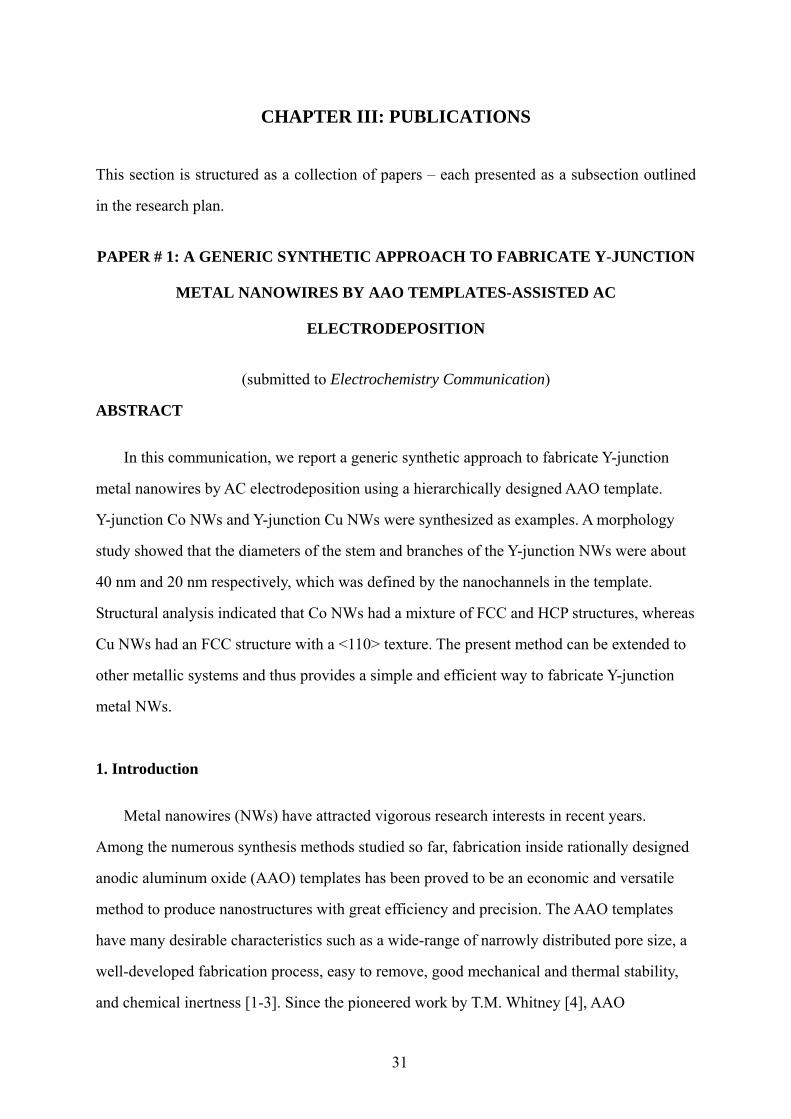
Fig. 1 Schematic of the process to synthesize Y-junction metal NWs.
Cobalt nanowires were electrochemically deposited by AC electrolysis in this
nanoporous template with Y-junction nanochannels using 14 Vrms at 100 Hz for 30 min in
an electrolyte solution consisting of 240 g l-1 of CoSO4·7H2O (Alfa Aesar), 40 g l-1 of HBO3
(Alfa Aesar), and 1 g l-1 of ascorbic acid (Alfa Aesar) [17-19]. Graphite was used as the
counter electrode. After Co deposition, AAO could be fully removed by etching with a 2 M
NaOH solution to obtain free standing Y-junction Co NWs.
The synthesis of copper nanowires was adapted from G.A. Gelves’s work [15,16].
Electrodeposition of the Y-junction Cu NWs was carried out in an aqueous solution
consisting of 0.50 M CuSO4 (Alfa Aesar) and 0.285 M H3BO3 by applying a continuous 200
Hz sine wave at 10Vrms for 10 min between the anodized Al and the graphite counter
electrode.
2.2 Materials characterization
XRD patterns were recorded on a Rigaku Miniflex diffractometer using a Cu Kα X-ray
source (1.5405 Å). The structure and morphology were characterized by SEM using a JEOL
JSM-7000F microscope and by TEM using a Phillips CM 12 operated at an accelerating
voltage of 120 kV. TEM samples were prepared as follows: first the Y-junction NWs were
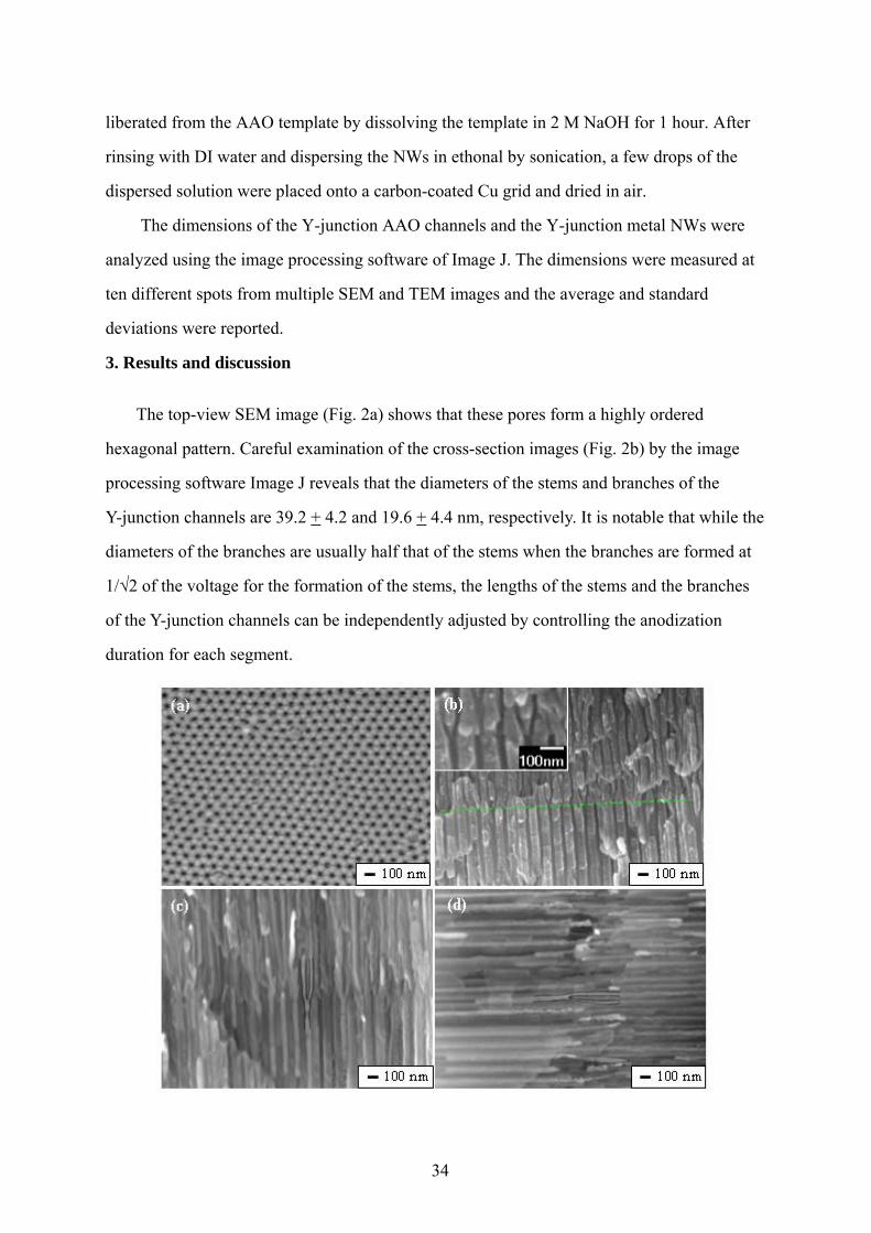
34
liberated from the AAO template by dissolving the template in 2 M NaOH for 1 hour. After
rinsing with DI water and dispersing the NWs in ethonal by sonication, a few drops of the
dispersed solution were placed onto a carbon-coated Cu grid and dried in air.
The dimensions of the Y-junction AAO channels and the Y-junction metal NWs were
analyzed using the image processing software of Image J. The dimensions were measured at
ten different spots from multiple SEM and TEM images and the average and standard
deviations were reported.
3. Results and discussion
The top-view SEM image (Fig. 2a) shows that these pores form a highly ordered
hexagonal pattern. Careful examination of the cross-section images (Fig. 2b) by the image
processing software Image J reveals that the diameters of the stems and branches of the
Y-junction channels are 39.2 + 4.2 and 19.6 + 4.4 nm, respectively. It is notable that while the
diameters of the branches are usually half that of the stems when the branches are formed at
1/√2 of the voltage for the formation of the stems, the lengths of the stems and the branches
of the Y-junction channels can be independently adjusted by controlling the anodization
duration for each segment.
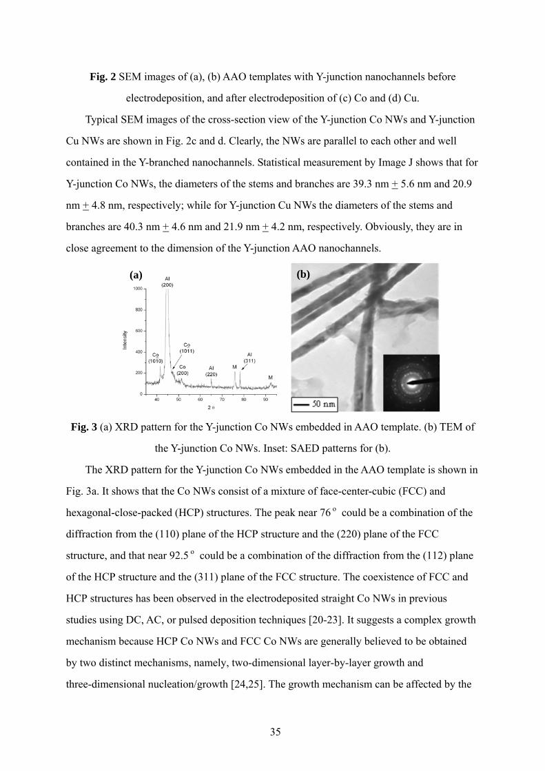
35
Fig. 2 SEM images of (a), (b) AAO templates with Y-junction nanochannels before
electrodeposition, and after electrodeposition of (c) Co and (d) Cu.
Typical SEM images of the cross-section view of the Y-junction Co NWs and Y-junction
Cu NWs are shown in Fig. 2c and d. Clearly, the NWs are parallel to each other and well
contained in the Y-branched nanochannels. Statistical measurement by Image J shows that for
Y-junction Co NWs, the diameters of the stems and branches are 39.3 nm + 5.6 nm and 20.9
nm + 4.8 nm, respectively; while for Y-junction Cu NWs the diameters of the stems and
branches are 40.3 nm + 4.6 nm and 21.9 nm + 4.2 nm, respectively. Obviously, they are in
close agreement to the dimension of the Y-junction AAO nanochannels.
Fig. 3 (a) XRD pattern for the Y-junction Co NWs embedded in AAO template. (b) TEM of
the Y-junction Co NWs. Inset: SAED patterns for (b).
The XRD pattern for the Y-junction Co NWs embedded in the AAO template is shown in
Fig. 3a. It shows that the Co NWs consist of a mixture of face-center-cubic (FCC) and
hexagonal-close-packed (HCP) structures. The peak near 76 o could be a combination of the
diffraction from the (110) plane of the HCP structure and the (220) plane of the FCC
structure, and that near 92.5 o could be a combination of the diffraction from the (112) plane
of the HCP structure and the (311) plane of the FCC structure. The coexistence of FCC and
HCP structures has been observed in the electrodeposited straight Co NWs in previous
studies using DC, AC, or pulsed deposition techniques [20-23]. It suggests a complex growth
mechanism because HCP Co NWs and FCC Co NWs are generally believed to be obtained
by two distinct mechanisms, namely, two-dimensional layer-by-layer growth and
three-dimensional nucleation/growth [24,25]. The growth mechanism can be affected by the
(a) (b)
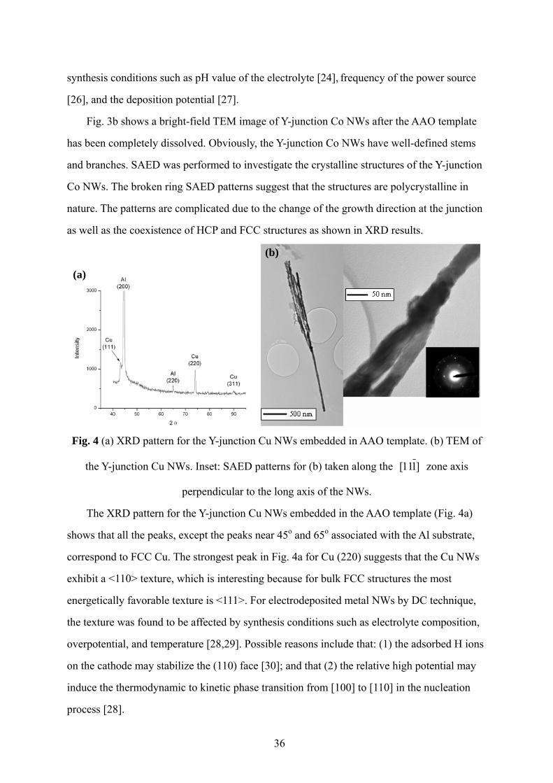
36
synthesis conditions such as pH value of the electrolyte [24], frequency of the power source
[26], and the deposition potential [27].
Fig. 3b shows a bright-field TEM image of Y-junction Co NWs after the AAO template
has been completely dissolved. Obviously, the Y-junction Co NWs have well-defined stems
and branches. SAED was performed to investigate the crystalline structures of the Y-junction
Co NWs. The broken ring SAED patterns suggest that the structures are polycrystalline in
nature. The patterns are complicated due to the change of the growth direction at the junction
as well as the coexistence of HCP and FCC structures as shown in XRD results.
Fig. 4 (a) XRD pattern for the Y-junction Cu NWs embedded in AAO template. (b) TEM of
the Y-junction Cu NWs. Inset: SAED patterns for (b) taken along the ]111[ zone axis
perpendicular to the long axis of the NWs.
The XRD pattern for the Y-junction Cu NWs embedded in the AAO template (Fig. 4a)
shows that all the peaks, except the peaks near 45o and 65o associated with the Al substrate,
correspond to FCC Cu. The strongest peak in Fig. 4a for Cu (220) suggests that the Cu NWs
exhibit a <110> texture, which is interesting because for bulk FCC structures the most
energetically favorable texture is <111>. For electrodeposited metal NWs by DC technique,
the texture was found to be affected by synthesis conditions such as electrolyte composition,
overpotential, and temperature [28,29]. Possible reasons include that: (1) the adsorbed H ions
on the cathode may stabilize the (110) face [30]; and that (2) the relative high potential may
induce the thermodynamic to kinetic phase transition from [100] to [110] in the nucleation
process [28].
(a)
(b)

37
Fig. 4b depicts the TEM images of Y-junction Cu NWs. Analysis by Image J shows that
the stem and branches of individual Y-junction Cu NWs have diameters of 42.8 + 7.4 nm and
35.8 + 5.3 nm, respectively. Similar analysis of TEM images of Y-junction Co NWs shows
that the diameters of the stem and branches are 42.2 nm + 4.0 nm and 28.1 nm + 4.2 nm,
respectively. Clearly, the diameters of the stems and branches of both metal NWs are larger
compared to the results estimated by SEM images. The dimension increase of the metal NWs
may be due to the surface oxidation during the template removal or TEM sample preparation
process [31]. The spotty diffraction rings in Fig. 4b (inset) show the polycrystalline nature of
the Cu NWs.
4. Conclusions
In summary, by using a hierarchically designed AAO template, we developed a generic
synthetic approach to fabricate Y-junction metal nanowires by AC electrodeposition. For the
Y-junction Co NWs and Y-junction Cu NWs fabricated in this communication, a morphology
study shows that well-defined Y-junctions were synthesized, and the dimensions of the NWs
were defined by the template. Structure analysis indicated that the Co NWs were a mixture of
FCC and HCP structures, and Cu NWs had FCC structure with a <110> texture. The present
method can be extended to other metallic systems and thus provides a simple and efficient
way to fabricate Y-junction metal NWs. Future work includes studying the effects of the
synthesis parameters such as potential, frequency, and temperature on the crystal structure of
the fabricated metal NWs.
Acknowledgment
The authors would like to thank Dr. Gregory Hendricks at University of Massachusetts
Medical School for his help with TEM. This work is supported in part by a NSF award
CMMI-0825990.
References
[1] H. Masuda, F. Hasegwa, S. Ono, J. Electrochem. Soc. 144 (1997) 127.
[2] A. P. Li, F. Muller, A. Birner, K. Nielsch, U. Gosele, J. Appl. Phys. 84 (1998) 6023.
[3] O. Jessensky, F. Muller, U. Gosele, Appl. Phys. Lett. 72 (1998) 1173.
[4] T. M. Whitney, J. S. Jiang, P. C. Searson, C. L. Chien, Science 261 (1993) 1316.
38
[5] J. Li, C. Papadopoulos, J. Xu, Nature 402 (1999) 253.
[6] G. Meng, Y. J. Jung, A. Cao, R. Vajtai, P. M. Ajayan, Proc. Natl. Acad. Sci. 102 (2005)
7074.
[7] T. Gao, G. Meng, J. Zhang, S. Sun, L. Zhang, Appl. Phys. A: Mater. Sci. Process. 74 (2002)
403.
[8] J. Choi, G. Sauer, K. Nielsch, R. B. Wehrspohn, U. Gosele, Chem. Mater. 15 (2003) 776.
[9] Y. Tian, G. Meng, S. K. Biswas, P. M. Ajayan, S. Sun, L. Zhang, Appl. Phys. Lett. 85
(2004) 967.
[10] S. Mahima, R. Kannan, I. Komath, M. Aslam, V.K. Pillai, Chem. Mater. 20 (2008) 601.
[11] A. J. Yin, J. Li, W. Jian, A. J. Bennett, J. M. Xu, Appl. Phys. Lett. 79 (2001) 1039.
[12] X. Y. Zhang, G. H. Wen, Y. F. Chan, R. K. Zheng, X. X. Zhang, N. Wang, Appl. Phys. Lett.
83 (2003) 3341.
[13] N. J. Gerein, J. A. Haber, J. Phys. Chem. B 109 (2005) 17372.
[14] R. L. Wang, S. L. Tang, B. Nie, X. L. Fei, Y. G. Shi, Y. W. Du, Solid State Comm. 142
(2007) 639.
[15] G. A. Gelves, B. Lin, U. Sundararaj, J. A. Haber, Adv. Funct. Mater. 16 (2006) 2423.
[16] G. A. Gelves, Z. T. Murakami, M. M. J. Krantz, J. A. Haber, J. Mater. Chem. 16 (2006)
3075.
[17] J. Liang, H. Chik, A. Yin, J. M. Xu, J. Appl. Phys. 91 (2002) 2544.
[18] J. Liang, H. Chik, J. M. Xu, IEEE J. Sel. Top. Quantum Electron. 8 (2002) 998.
[19] J. Li, C. Papadopoulos, J. M. Xu, M. Moskovits, Appl. Phys. Lett. 75 (1999) 367.
[20] F. Li, T. Wang, L. Ren, J. Sun, J. Phys.: Condens. Matter. 16 (2004) 8053.
[21] G. Tourillon, L. Pontonnier, J. P. Levy, V. Langlais, Electrochem. Solid-State Lett. 3
(2000) 20.
[22] G. J. Strijkers, J. H. J. Dalderop, M. A. A. Broeksteeg, H. J. M. Swagten, W. J. M. de Jonge,
J. Appl. Phys. 86 (1999) 5141.
[23] N. R. Pradhan, H. Duan, J. Liang, G. S. Iannacchione, Nanotechnology 19 (2008) 485712.
[24] H. Pan, H. Sun, C. Poh, Y. Feng, J. Lin, Nanotechnology 16 (2005) 1559.
[25] M. Tian, J. Wang, J. Kurtz, T. E. Mallouk, M. H. Chan, Nano Lett. 3 (2003) 919.
[26] J. Zhang, G. A. Jones, T. H. Shen, S. E. Donnely, G. Li, J. Appl. Phys. 101 (2007) 054310.
[27] X. W. Wang, G. T. Fei, P. Tong, X. J. Xu, L. D. Zhang, J. Crystal Growth 300 (2007) 421.
[28] J. A. Switzer, H. M. Kothari, E. W. Bohannan, J. Phys. Chem. B 106 (2002) 4027.
[29] H. Pan, B. Liu, J. Yi, C. Poh, S. Lim, J. Ding, Y. Feng, C. H. A. Huan, J. Lin, J. Phys.
Chem. B 109 (2005) 3094.

39
[30] E. Budevski, G. Staikov, W. Lorenz, J. Electrochemical Phase Formation and Growth: An
introduction to the initial stage of metal deposition, VCH: New York, 1996 (Chapter 6).
[31] N. J. Gerein, J. A. Haber, J. Phys. Chem. B 109 (2005) 17372.

40
PAPER # 2: SYNTHETIC HIERARCHICAL NANOSTRUCUTRES: GROWTH OF
CARBON NANOFIBERS ON MICROFIBERS BY CHEMICAL VAPOR
DEPOSITION
(submitted to Materials Science and Engineering B)
ABSTRACT
Hierarchical structures were synthesized by thermally decomposing acetylene to grow
carbon nanofibers (CNFs) on carbon microfibers and glass microfibers using catalytic
chemical vapor deposition. A sulfonated silane intermediary was used to uniformly disperse
Ni-Co (1:1) catalysts on the microfibers. The CNFs were grown on glass microfibers and
carbon microfibers at 600 oC and 800 oC, respectively. An acetylene and nitrogen mixture
(volume ratio 1:9) was used as a carbon source. The nanofiber morphology and structure
were analyzed by scanning electron microscopy and high resolution transmission electron
microscopy. As-prepared CNFs grown on both substrates typically have two types of
morphology, coil-like with no distinct orientation and relatively straight and long CNFs. The
diameter of CNFs on carbon fibers is 176 + 5.8 nm compared to 71.82 + 26.38 nm on glass
fibers. CNFs grow more densely on carbon microfibers than on glass microfibers, which is
affected by different surface chemistry and growth temperature. This hierarchical
nanostructure with CNFs anchored to the carbon fibers and/or glass fibers offers a method to
integrate nanoscale entities with materials or devices with larger length scales and may find
applications as electrodes in fuel cells, sensors, supports for catalysts, and reinforcing
components for composite materials.
1. Introduction
Carbon nanostructures have emerged as a new and attractive class of materials with
unique electrical, mechanical, physical, and chemical properties [1,2]. They are actively
studied for applications such as nanoelectronic devices [3-5], Li battery electrode material [6],
field emission displays [7], storage materials for hydrogen and other gases [8], and probe tips

41
for atomic force microscopy (AFM) [9]. A lot of research work has focused on carbon
nanotube (CNT) preparation techniques [10-14], theoretical simulation to understanding the
physics of carbon nanostructures [15-18], and CNT post-treatments such as purification,
thermal annealing, and surface modification [19-21]. However, the effective integration of
carbon nanostructures with materials and devices of larger length scales to fully exploit the
benefit of carbon nanostructures remains a major obstacle. Synthesis of hierarchical
structures by anchoring carbon nanostructures to micron-scaled substrates offers a
straightforward pathway to connect the nanostructures to the higher hierarchy.
In addition, the carbon-based hierarchical structures are expected to provide
advantageous properties for many applications. For example, as catalyst support of Pt
particles for proton exchange membrane fuel cells, they may improve the Pt utilization by
securing the electronic route from Pt to the supporting electrode [22]. Thostenson
demonstrated that by covering individual carbon fibers (CFs) with a sheath of CNTs and
embedding this structure in a polymer matrix, the nanocomposite reinforcement resulted in
local stiffening near the fiber/matrix interface and improved the interfacial shear strength [23].
S. Lim et al grew carbon nanofibers (CNFs) on activated CFs and used this composite to
improve the efficiency of SOx and NOx removal [24]. Similar carbon hierarchical structures
were studied for drinking water purification by selective chemisorptions of chromate and
heteropolymolybdate [25].
Catalytic chemical vapor deposition (CCVD) is a popular fabrication method to
synthesize carbon nanostructures. It is known that the properties of synthesized carbon
materials, such as surface structure, morphology (fibers or tubes), diameter, length, shape,
and texture, can be varied by controlling the catalyst precursor and synthesis parameters
including the temperature schedule, carbon source, and gas flow rate [26]. CCVD has been
successfully employed to grow CNTs and CNFs on many planar substrates such as silicon,
silica and alumina [27-30]. More recently, a few studies on growing CNTs or CNFs on
substrates with micron-scaled features including carbon paper, steel mesh, and primary CNTs
by CCVD for various purposes have been reported [31-34].
In the present work, we demonstrate successful CNF growth on individual carbon
microfibers as well as individual glass microfibers by CCVD technique. The growth

42
conditions and their influence on the nanofiber morphology are discussed. As-grown
three-dimensional carbon-carbon and carbon-glass hierarchical structures may find
applications in electrodes for fuel cells, sensors, supports for catalysts, and reinforcing
components for composite materials.
2. Experimental
2.1 Synthesis of CNFs
CNFs were synthesized by decomposing acetylene on catalytic Co/Ni particles deposited
on the CF fabrics (Ernest F. Fullam Inc., Latham, New York) or glass fibers (GFs) (Corning
Inc., Corning, New York). The fabrication process is depicted in Fig. 1.
Fig. 1 The fabrication of hierarchical CNF-CF/GF structures.
As shown in Fig. 1, prior to catalyst deposition, the CFs and GFs were pre-treated by
immersing them in ethanol for 30 min. This treatment helps to improve the homogeneity of
the catalytic Co/Ni particle size on the fibers [32]. Ni-Co catalysts were then deposited by
solution dipping. First, 2(4-chlorosulfonylphenyl) ethyl trichlorosilane 50 vol% in
dichloromethane (United Chemical Technologies) was diluted by 6 vol% water in ethanol to
obtain a final silane concentration of 1 vol% [35]. This solution was stirred for 2 hours at
room temperature. Then Co and Ni sulfates with a 1:1 molar ratio were added to the solution
and stirred for another 30 min. to form a saturated solution. CFs and GFs were soaked in the
catalyst solution for 10 sconds to load the catalyst precursor. The extra solution on the fibers
was wiped off with a lint free tissue.
After the CFs and GFs were loaded with the catalyst precursor, they were placed in a
ceramic boat and loaded into the center of the CVD chamber. CNFs were grown by CCVD.
Dipping in the catalyst precursor
solution
Fibers with catalyst precursor
Reduction to form catalyst nanoparticles
CNF-CF/GF hierarchical structures
CCVD for CNF growth
Surface modified fibers
PretreatmentCarbon fibers or
Glass fibers

43
The samples were first heated in Ar to 400 oC at a rate of 10 oC min-1 and kept at 400 oC for
10 min to decompose the sulfonated silanes. Then the catalyst precursors were reduced at 550 oC for 2.5 min by carbon monoxide to obtain metallic catalyst nanoparticles. After catalyst
reduction, the system was heated in Ar up to 600 oC and 800 oC for GFs and CFs, respectively.
CNFs were grown by pyrolysis of 10 vol% acetylene in N2 at those high temperatures for 5
min. Finally, the system was cooled to room temperature in an Ar atmosphere.
2.2 Characterization
The morphology of the as-prepared hierarchical structure was observed by a field
emission scanning electron microscope (FE-SEM, JOEL LEO 982) operated at 5 keV. The
microstructures of the CNFs was characterized by a high-resolution transmission electron
microscope (HRTEM, JOEL, JEM2100) operated at 200 kV. The specimens for the TEM
analysis were prepared by dispersing the samples in ethanol using ultrasonic treatment at
room temperature. The diameters of the CNFs on both microfiber substrates were obtained by
using the image processing software of Image J to analyze the SEM images of CNFs at
40,000X magnification or higher [36]. The dimensions were determined by measuring the
diameter at five different locations on each of ten randomly selected carbon nanofibers from
every sample and the average and standard deviations were reported.
3. Results and discussion
3.1 Growth of CNFs on the CF surface
Fig. 2 shows the typical SEM images of the CFs before CNF growth and the as-prepared
CNFs grown on the CFs. Clearly, the CF surface is covered by a dense layer of coil-like
CNFs without any distinct orientation, which doubled the diameter of the CFs. Though the
lack of orientation makes the length measurement difficult, the observed length of CNFs is at
least tens of micrometers after 5-min growth, which suggests a high growth rate. Fig. 2c is a
typical SEM image of as-prepared CNFs at higher magnification. Analysis by Image J shows
that the mean diameter of the CNFs is 176 nm with a standard deviation of 5.8 nm. Thus the
as-prepared CNFs are rather uniform in diameter, which implies uniform distribution of the
catalyst particles on the carbon surfaces after the catalyst impregnation. Moreover, as shown
in Fig. 2c, the surface of each single CNF is smooth. Amorphous carbon covering the CNF

44
surface [32] has not been observed in any of the CNFs, indicating that the selection of
experimental conditions can be efficient to prevent amorphous carbon from forming.
Fig. 2 (a) SEM image of CF before CNF growth, (b) and (c) SEM images of CNFs grown on
the surface of CFs, scale bar: (a)1 μm, (b)2 μm, and (c)100 nm.
The CNFs were detached from the CF substrate and dispersed in the ethanol by 10-min
sonication for the TEM study. Fig. 3 depicts the TEM images of CNFs grown on the surface
of CFs. It confirms that there is no amorphous carbon on the surface of the as-prepared CNFs.
In addition, it is interesting to note that the CNFs exhibit two different types of
microstructures. In the first type, as shown in Fig. 3a and b, the spiral shaped twisted CNFs
wind a lot without showing a distinct growth direction. Careful examination of Fig. 3 shows
that the coiled CNFs are not well ordered and the graphite sheets exist in a distorted
“herring-bone” arrangement, which is consistent to previous studies on CNFs of similar
morphology [37,38]. In contrast, in the second type, as shown in Fig. 3c, fibers that are
relatively straight and long without frequent direction change have been observed, which
suggests a smooth growth process. An HRTEM image (Fig. 3d) shows that the nanofibers are
better ordered than the coiled CNFs and the graphite sheets tend to be aligned in a direction
parallel to the fiber growth axis.

45
Fig. 3 TEM micrographs of carbon nanofibers grown on the surface of CFs with
microstructure of (a), (b) type 1 and (c), (d) type 2, scale bar: (a) 500 nm, (b) 100 nm, (c) 500
nm, and (d) 5 nm.
According to the quasi-Vapor Liquid Solid (VLS) growth mechanism [26], CVD growth
of CNFs involves the following steps: (1) carbon atoms are produced through acetylene
decomposition; (2) the freshly formed carbon atoms near the catalyst particles immediately
dissolve into the catalyst particles; (3) when saturation reaches within the catalyst particles,
carbon in the form of graphite sheets precipitates along different precipitating planes of the
catalyst particles to form CNFs. The arrangement of the graphite sheets in CNFs is generally
believed to be controlled by the orientation of the precipitating planes of the metal particles.
A simplified model for the two different graphite sheet arrangements, i.e. parallel and
herring-bone arrangements, is shown in Fig. 4. If carbon precipitates along a pair of adjacent
planes at the same rates, straight herring-bone structured CNFs (Fig. 4a) will form with the
graphite platelets aligned at an angle to the filament axis. If the graphite precipitates along the

46
lateral planes of the catalyst particles at the same rates, parallel structured CNFs (Fig. 4b)will
be obtained with the platelets aligned in a direction parallel to the filament axis [39].
However, when the carbon precipitates along different planes of the catalyst particles at
different rates, the CNF may bend to the direction with the lower precipitation rate. The
growth direction of the CNFs changes during growth, producing the spiral shaped CNF
structures (Fig. 4 c and d). Possible reasons causing varying deposition and precipitation rates
for different catalyst planes include: (1) different catalytic ability for different crystal planes
[40,41], (2) asymmetrical shaped catalyst particles which lead to different diffusion path
lengths for the carbon atoms to traverse [42], and (3) a nonuniform carbon supply. In the
current study, the coexistence of both distorted herring-bone and parallel nanofibers suggests
a complex growth mechanism.
Fig. 4 Schematic of the structures of straight and distorted herring-bone (a, c) and parallel (b,
d) type carbon nanofibers.
3.2 Growth of CNFs on the GF surface
To study how the change of surface chemistry will affect CNF growth, GFs were
selected as a non-carbon substrate with micro-scaled features in our fabrication approach.
GFs, one of the most versatile industrial materials, are widely used in the manufacture of
structural composites, printed circuit boards, and a wide range of special-purpose products
[43]. Since carbon nanostructures had previously been successfully grown on silica [44], we
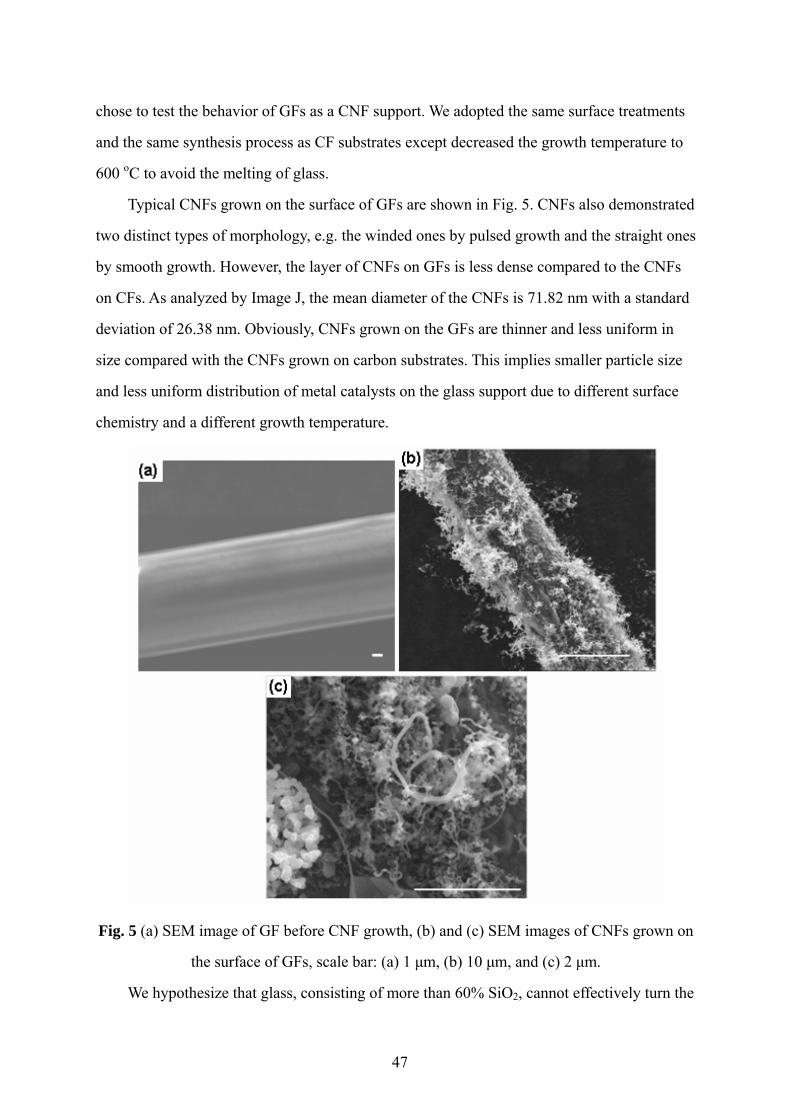
47
chose to test the behavior of GFs as a CNF support. We adopted the same surface treatments
and the same synthesis process as CF substrates except decreased the growth temperature to
600 oC to avoid the melting of glass.
Typical CNFs grown on the surface of GFs are shown in Fig. 5. CNFs also demonstrated
two distinct types of morphology, e.g. the winded ones by pulsed growth and the straight ones
by smooth growth. However, the layer of CNFs on GFs is less dense compared to the CNFs
on CFs. As analyzed by Image J, the mean diameter of the CNFs is 71.82 nm with a standard
deviation of 26.38 nm. Obviously, CNFs grown on the GFs are thinner and less uniform in
size compared with the CNFs grown on carbon substrates. This implies smaller particle size
and less uniform distribution of metal catalysts on the glass support due to different surface
chemistry and a different growth temperature.
Fig. 5 (a) SEM image of GF before CNF growth, (b) and (c) SEM images of CNFs grown on
the surface of GFs, scale bar: (a) 1 μm, (b) 10 μm, and (c) 2 μm.
We hypothesize that glass, consisting of more than 60% SiO2, cannot effectively turn the
48
orientation of the CH3 group in ethanol towards the glass surface to become more hydrophilic
like carbon does during the pretreatment in ethanol [45]. Another reason may be the relatively
weak catalytic effect of Ni-Co nanoparticles when they are on glass substrate. Though there is
no report directly comparing impact of surface chemistry of carbon and glass, R.L. Vander
Wal et al pointed out that Ni is far less catalytically active when supported on SiO2 than
supported on TiO2 [28]. Moreover, silica may not serve as a negative charge donator to make
a strong interaction between the Ni-Co alloy particles and the silica substrate.
4. Conclusions
In this article, we demonstrate the successful CNF growth on individual CFs and GFs to
form a three-dimensional hierarchical structure using a CCVD technique. CNFs grown on
both CFs and GFs demonstrated coexistence of two types of morphology. One is winded
fibers implying frequent orientation change. The other one is relatively straight and long
fibers with graphene sheets parallel to each other. This observation indicates the complex
growth mechanisms. CNFs grown on CMF substrate appear to be thicker and more uniform
than those on GMF substrates probably due to different catalyst-substrate interaction and
different growth temperature. The as-grown three-dimensional carbon-carbon and
carbon-glass hierarchical structures provide an effective means to connect nanoscale entities
to the higher hierarchy. They may find applications in the fields of fuel cells, sensors,
supports for catalysts, and reinforcing components for composite materials.
Acknowledgements
The authors would like to thank the National Nanotechnology Infrastructure
Network/Center for Nanostructured Systems at Harvard University for use of their
microscopy facilities. The work was supported in part by a NSF award CMMI-0825990.
Reference
[1] H. Dai, J.H. Hafner, A.G. Rinzler, D.T. Colbert, R. Smalley, Nature 384 (1996) 147-150. [2] L. Forro, C. Schnonenberger, in: M.S. Dresselhouse, G. Dresselhouse, P. Avouris (Eds),
Carbon nanotubes: synthesis, structure, properties and application, Springer, New York,
2001.
49
[3] T. Hertel, R. Martel, P. Avouris, J. Phys. Chem. B 102 (1998) 910-915.
[4] C. Bower, W. Zhu, D. Shalom, D. Lopez, L.H. Chen, P.L. Gammel, S. Jin, Appl. Phys.
Lett. 80 (2002) 3820-3822.
[5] K.B. Teo, M. Chhowalla, G.A. Amaratunga, W.I. Miline, P. Legagneux, G. Pirio, L.
Gangloff, D. Pribat, V. Semet, V.T. Binh, W.H. Bruenger, J. Eichholz, H. Hanssen, D.
Friendrich, S.B. Lee, D.G. Hasko, H. Ahmed, J. Vac. Sci. Technol. B 21 (2003) 693-697. [6] B. Gao, A. Kleinhammes, X. Tang, C. Bower, L. Fleming, Y. Wu, O. Zhou, Chem. Phys.
Lett. 307 (1999) 153-157.
[7] Y. Saito, K. Hamaguchi, K. Hata, K. Tohji, A. Kasuya, Y. Nishina, K. Uchida, Y. Tasaka, F.
Ikazaki, M. Yumura, Ultramicroscopy 73 (1998) 1-6.
[8] G.E. Gadd, M. Blackfold, S. Moricca, N. Webb, P.J. Evans, A.M. Smith, G. Jacobsen, S.
Leung, A. Day, Q. Hua, Science 277 (1997) 933-936.
[9] S.S. Wong, J. D. Harper, P.T. Lansbury, C.M. Lieber, J. Am. Chem. Soc. 120 (1998)
603-604. [10] T.W. Ebbesen, P.M. Ajayan, Nature 358 (1992) 220–222.
[11] A. Thess, R. Lee, P. Nikolaev, H. Dai, P. Petit, J. Robert, C. Xu, Y.H. Lee, S.G. Kim, A.G.
Rinzler, D.T. Colbert, G.E. Scuseria, D. Tomanek, J.E. Fischer, R.E. Smalley, Science 273
(1996) 483–487.
[12] H. Dai, in: M.S. Dresselhouse, G. Dresselhouse, P. Avouris (Eds), Carbon nanotubes:
synthesis, structure, properties and application, Springer, New York, 2001, p. 29–54.
[13] F. Ren, Z.P. Huang, J.W. Xu, J.H. Wang, P. Bush, M.P. Siegal, P.N. Provencio, Science
282 (1998) 1105–1107.
[14] B.O. Boskovic, V. Stolojan, R.U.A. Khan, S. Haq, S.R.P. Silva, Nat. Mater. 1 (2002)
165–168.
[15] A. Maiti, J. Zelm, A. Svizhenko, M.P. Anantram, M. Panhuis, Phys. Status Solidi B233
(2002) 49-58.
[16] I. Efremenko, M. Sheintuch, Langmuir 21 (2005) 6282-6288.
[17] VI. A. Margulis, E.E. Muryumin, O.B. Tomilin, Physica B 353 (2004) 314-323.
[18] T. Natsuki, M. Endo, Carbon 42 (2004) 2147-2151.
[19] C. Li, H. Liu, S. Tseng, Y. Lin, S. Chen, J. Li, K. Wu, J. Juang, Diam. Relat. Mater. 15
(2006) 2010-2014.
[20] J. Han, S.H. Lee, A.S. Berdinsky, Y.W. Kim, J. Yoo, C. Park, J.J. Choi T. Jung, I.T. Han,
J.M. Kim, Diam. Relat. Mater. 14 (2005) 1891-1896.

50
[21] S. Tzeng, K. Hung, T. Ko, Carbon 44 (2006) 859-865.
[22] C. Wang, M. Waje, X. Wang, J.M. Tang, R.C. Haddon, Y. Yan, Nano Lett. 4 (2004)
345-348.
[23] E.T. Thostenson, W.Z. Li, D.Z. Wang, Z.F. Ren. T.W. Chou, J. App. Phys. 91 (2002)
6034-6037.
[24] S. Lim, S. Yoon, Y. Shimizu, H. Jung, I. Mochida, Langmuir 20 (2004) 5559-5563.
[25] D.S. Su, X. Chen, G. Weinberg, A. Klein-Hofmann, O. Timpe, S.B.A. Hamid, R. Schlogl,
Angew Chem. Int. Ed. 44 (2005) 5488-5492.
[26] K.P. Jong, J W. Geus, Catal. Rev. Sci. Eng. 42 (2000) 481-510.
[27] R.L. Ver Wal, T.M. Ticich, V.E. Curtis, Carbon 39 (2001) 2277-89.
[28] X.J. Dai, C. Skourtis, J. Appl. Phys. 103 (2008) 124305.
[29] J.M. Simmons, B.M. Nichols, M.S. Marcus, O.M. Castellini, R.J. Hamers, M.A. Eriksson,
Small 7 (2006) 902-909.
[30] A. Cao, P.M. Ajayan, G. Ramanath, R. Baskaran, K. Turner, Appl. Phys. Lett. 84 (2004)
109-11.
[31] X. Sun, R. Li, B. Stansfield, J.P. Dodelet, S. Desilets, Chem. Phys. Lett. 394 (2004)
266–70. [32] L. Qu, Y. Zhao, L. Dai, Small 8-9 (2006) 1052–1059.
[33] K. Otsuka, Y. Abe, N. Kanai, Y. Kobayashi, S. Takenaka, E. Tanabe, Carbon 42
(2004)727-736. [34] W. Xia, X. Chen, S. Kundu, X. Wang, G .Grundmeier, Y. Wang, M. Bron, W. Schuhmann,
M. Muhler, Surf. Coat. Tech. 201 (2007) 9232-9237.
[35] X. Sun, B. Stansfield, J.P. Dodelet, S. Desilets, Chem. Phys. Lett. 363 (2002) 415–421.
[36] http://rsb.info.nih.gov/ij/
[37] G. Zheng, K. Kouda, H. Sano, Y. Uchiyama, Y. Shi, H. Quan, Carbon 42 (2004) 635-640.
[38] O.C. Carneiro, N.M. Rodriguez, R.T.K. Baker, Carbon 43 (2005) 2389-2396.
[39] N. Krishnankutty, C. Park, N.M. Rodriguez, R.T.K. Baker, Cata. Today 37 (1997)
295-307.
[40] M. Kawaguchi, K. Nozaki, S. Motojima, H. Iwanaga, J. Crystal Growth 3-4 (1992)
309-313.
[41] Y. Wen, Z. Shen, Carbon 39 (2001) 2369-2386.
[42] S.P. Sharma, S.C. Lkkad, Surf. Coat. Tech. 203 (2009) 1329-1335.
[43] F.T. Wallenberger, Proc. Of the Norbert Kreidl Symposium (Triensberg, Liechtenstein),

51
1994, p 63-78.
[44] S. Takenaka, S. Kobayashi, H. Ogihara, K. Otsuka, J. Catal. 217 (2003) 79-87.
[45] X. Sun, R. Li, G. Lebrun, B. Stanfield, J.P. Dodelet, Int. J. Nanosci. 1 (2002) 223-234.
52
PAPER # 3: NOVEL GROWTH MORPHOLOGY OF CATHODICALLY
ELECTRODEPOSITED Fe3O4 THIN FILMS
(submitted to Thin Solid Films)
ABSTRACT
We report on the electrodeposition of Fe3O4 thin films in the Fe3+-triethanolamine system
by galvanostatic deposition. It was observed that both the deposition rate and the surface
morphology of the Fe3O4 thin films were dependent upon the deposition temperature, Fe3+
ion concentration, and deposition time. Fe3O4 thin films deposited in electrolyte with high
Fe3+ concentration at high temperature (>80 oC) exhibited a dense and uniform morphology
and were composed of globular or polyhedral crystallites, while the Fe3O4 deposited at low
temperatures (<70 oC) were loose and flake-like. Based on the empirical observations, a
hypothetical growth mechanism is proposed.
Keywords: galvanostatic electrodeposition, Fe3O4, thin film, morphology,
Fe3+-triethanolamine complex.
Fe3O4 is the first known magnetic material and has been investigated extensively due to
its technological applications in recording media, corrosion and catalysis. The renewed
interests in Fe3O4 in past few years lie on its potential applications in magnetic memory and
giant magnetoresistance (GMR) sensors [1-3]. More recently, Fe3O4 was studied as an
electrode material for Li ion batteries because theoretically it can react with eight Li ions per
formula unit at a potential of 1.5 V versus Li+/Li0 and thus have a high specific capacity
[4-6].
Fe3O4 thin films have been grown on polycrystalline and single-crystal substrates by a
variety of deposition techniques such as laser ablation [7-11], molecular beam epitaxy (MBE)
[12-14], oxidizing Fe thin films [15-17], evaporation [18,19], and sputtering [20,21].
Although these vacumm-based methods provide good control over film thickness,
morphology, crystallinity, and purity, they require costly equipment. Often the deposition
involves prolonged evacuation of the vacuum system and heating of both the target and

53
substrate, which consumes considerable amounts of energy. The aqueous solution-based
electrodeposition approach can be performed at a relatively low temperature and low cost,
and is easy to control. Moreover, electrochemical deposition is a versatile process and can be
used to fabricate not only Fe3O4 thin films, but Fe3O4 nanoparticles [22] and Fe3O4 nanowire
arrays [23-25].
There are two basic approaches to grow Fe3O4 films by electrodeposition, i.e. anodic
deposition in Fe2+ systems and cathodic deposition in Fe3+ systems. The majority of the
previous work was conducted in the Fe2+ systems [23,24,26-30] where Fe2+ ion were
complexed with organic compounds such as acetate anion and were electrochemically
oxidized to form Fe3O4 in inert atmosphere at elevated temperature. A problem with this
method is that the complexed Fe2+ tends to get oxidized by molecular oxygen in the air, so
special attention must be paid to exclude molecular oxygen. Recently, based on the
hydrothermal method by Sapieszko and Matijevic [31], cathodic reduction of Fe3+ complexed
with triethanolamine (TEA) was proposed to deposit Fe3O4. In this approach, it is not
necessary to eliminate molecular oxygen from the deposition environment [32]. This method
was further used by J.M. Tarascon’s group to fabricate Fe3O4 electrode for Li ion batteries
[5,6]. However, no systematic study has been reported regarding factors affecting the Fe3O4
deposition in the Fe3+-TEA system such as temperature, Fe3+-TEA concentration, and time.
In addition, the morphology of electrodeposited Fe3O4 fabricated by different researchers
is not consistent. Chung et al. reported a porous nano-sized cellular Fe3O4 thin film on a Pt
substrate at room temperature [27]. Martinez et al. observed an adherent and homogeneous
Fe3O4 film consisting of polyhedral crystals at 90 oC [29]. Magnetite deposits with particle
size around 82 nm were obtained by Franger at room temperature [22]. Chatman et al. found
that the electrolyte composition could change the magnetite morphology from angular
crystallite to round and columnar crystallites at temperatures between 60 oC to 85 oC [28].
Globular, pyramidal, and needle-shaped morphologies were reported for Fe3O4 deposited at
60 oC to 90 oC [5,32]. Here we report a systematic investigation of the Fe3O4 deposition, the
morphology and the deposition rate in the Fe3+-TEA systems with Fe3+ concentration ranging
from 0.02 M to 0.08 M at various temperatures. The microstructure and morphology of the
Fe3O4 deposits were obtained using a field-emission gun scanning electron microscope

54
(SEM).
Experimental
Fe3O4 was deposited in an alkaline solution of Fe2(SO4)3·5H2O (Acros Organics, 97%
purity) stabilized by TEA (Sigma Aldrich, reagent grade). NaOH (Fisher Scientific, A.C.S.
grade) was used to adjust the pH value of the deposition bath. All chemicals were used
without further purification. The solution was made by adding Fe3+ solution dropwise into a
mixture of stirred TEA and NaOH solutions at 60 oC. The compositions of the final solutions
tested in this study before complexion reactions are given in Table 1.
Table 1. Composition of the investigated complex solutions
Solutions C (Fe3+)/ mol l-1 C (TEA)/ mol l-1 C (NaOH)/ mol l-1
1 0.02 0.1 1
2 0.04 0.1 1
3 0.06 0.1 1
4 0.07 0.1 1
5 0.08 0.1 1
Fe3O4 electrodeposition on Cu electrodes was performed galvanostatically at a current
density of -5 mA cm-2 using a two-electrode set-up. A Keithley Model 228A served as the
power source. The working electrode was a planar Cu disc (1.3 cm in diameter, from Yardney
Lithion, Inc., used as received) with a geometric area of 1.33 cm2. The Cu disc was cleaned
with acetone, diluted HCl solution (1:9 in vol. ratio with water), and deionized (DI) water
before deposition. The backside of the disc was insulated with nail polish. This nail polish
coating was removed with acetone and isopropanol after deposition. The counter electrode
was a graphite sheet. All the depositions were conducted with stirring in air unless otherwise
specified. After rinsing the Fe3O4 deposits with DI water and drying them in air, the structure
and morphology was characterized without further treatment. The weight of the deposited
iron oxide films was measured by a METTLER H54AR Analytical Balance with an accuracy
of 0.01 mg, and the deposition rates were estimated by measuring the weight of deposits per
unit area as a function of time.
55
Fe3O4 thin films were examined using a Bruker axs D8 Focus X-ray diffractometer (XRD)
and a JEOL JSM-7000F field-emission gun scanning electron microscope (SEM) equipped
with Oxford INCA Energy 250 energy-dispersive X-ray spectrometer (EDS).
Results and discussion
Preparation of Fe3+-TEA Solutions.— TEA has been used as a complexing agent for Fe2+
and Fe3+ ions for decades [33,34]. The poly-valent iron ions, which normally are converted
into insoluble hydrated iron oxides in strongly alkaline solutions, tend to react with the basic
TEA to form metal salts with liberation of water [34]. Both the pH value and the metal to
ligand ratio are critical to forming a stable complex solution. In the present work, we kept the
NaOH and TEA concentrations constant and employed solutions with Fe3+ concentrations
that were varyied from 0.02 to 0.08 mol l-1. When the Fe3+ concentration was less than 0.07
M, and Fe3+ solution was added dropwise to the NaOH and TEA solution mixture a small
amount of local precipitation formed which eventually dissolved with stirring to give clear
and pale greenish final solutions. However, when the Fe3+ concentration was increased to
0.08 M, a small amount of brown precipitate was observed in the final solution which did not
dissolve even after stirring for several hours.
The effect of temperature and concentration on the deposition rate.— Fig. 1 shows the
Fe3O4 deposition rates in different Fe3+ solutions at 60 oC and 80 oC, respectively. The
depositions were carried out at a constant current density of -5 mA cm-2. For all the
deposition conditions tested, the weight gain per unit electrode area exhibits a good linear
trend with respect to the deposition duration. The disposition rate is strongly affected by
temperature. In solution 5, for instance, the deposition rate at 80 oC is more than two times
greater than that at 60 oC.
As shown in Fig. 1, the deposition rate is strongly dependent on the Fe3+ ion
concentration as well. At 80 oC, the minimum Fe3+ ion concentration is 0.02 M to obtain a
considerable amount of Fe3O4 deposits. Above 0.02 M, more concentrated solutions result in
greater deposition rates. In solution 5, which contains 0.08 M Fe3+, the deposition rate is
estimated to be 0.32 mg cm-2 min-1, which is about two and three times greater than that in
solutions containing 0.07 M and 0.04 M Fe3+ respectively. From this we can conclude that

56
high Fe3+ concentration and high deposition temperature are necessary to achieve fast Fe3O4
deposition, which is desirable for large-scale Fe3O4 deposition.
0 100 200 300 400 500 6000.0
0.5
1.0
1.5
2.0
2.5
3.0
3.5
4.0
4.5W
eigh
t gai
n pe
r uni
t are
a (m
g/cm
2 )
Deposition time (s)
0.08 M Fe3+ at 80 oC 0.08 M Fe3+ at 60 oC 0.07 M Fe3+ at 80 oC 0.04 M Fe3+ at 80 oC 0.02 M Fe3+ at 80 oC
Fig. 1 The Fe3O4 deposition rates in different solutions at 60 oC and 80 oC.
The effect of temperature on the deposit morphology.— Fig. 2 demonstrates the
morphology evolution of the Fe3O4 films deposited in solution 5 at a constant current of -5
mA cm-2 for 120 s at 60 oC, 70 oC, 80 oC, and 90 oC, respectively. Clearly, the morphology
differs significantly at different deposition temperatures. The deposits at lower temperatures
such as 60 oC and 70 oC are usually loose and have a flake-like morphology, while those at
higher temperatures such as 80 oC and 90 oC are denser and have a particle-like morphology.
Specifically, after 120 s deposition at 60 oC (Fig. 2a and b), a very thin layer of flake-like
porous Fe3O4 film formed continuously and uniformly over the Cu substrate, which looks
similar to the morphology of Fe3O4 films deposited on Pt substrates at room temperature by
Chung et al [27]. When the deposition temperature was 70 oC (Fig. 2c and d), thicker but still
loose deposits were obtained due to an increased deposition rate at a higher temperature.
Severe cracking observed in Fig. 2c and d may be attributed to the shrinkage of the loose
deposits during drying as suggested by other studies [35,36]. At 80 oC (Fig. 2e and f),
globular particles began to form and the final deposits turned out to be dense and crack-free,
and consisted of a mixture of flakes and particles. No flakes formed during deposition at 90

57
oC (Fig. 2g and h), and the magnetite deposits exhibited well-defined crystal morphology
with crystal size in the range of 100 nm to 500 nm. This trend of getting better-defined
crystallites at higher deposition temperature agrees well with the previously reported
morphology results [5,28,29,32].
Fig. 2 SEM images of the Fe3O4 films deposited on the planar Cu substrates at (a), (b) 60 oC,
(c), (d) 70 oC, (e), (f) 80 oC, and (g), (h) 90 oC. The films were deposited at a current density
(a) (b)
(g) (h)
(c) (d)
(e) (f)
10μm
10μm
10μm
10μm
1μm
1μm
1μm
1μm

58
of -5 mA cm-2 in solution 5 for 120 s.
The effect of deposition time on the deposit morphology.—The morphology of Fe3O4
films that resulted from extending the electrodeposition time to 360 s, is depicted in Fig 3.
Fig. 3a and c show similar cracking morphology for the deposits obtained at 60 oC and 70 oC.
At 60 oC as the deposition time increased, cracks began to occur and the continuous film
formed at the beginning of the deposition (Fig. 2a and b) was broken down into islands. Each
of these islands looked similar and was composed of porous magnetite flakes as shown in Fig.
3b. When the deposition time was increased further to 720 s (morphology not shown), the
cracking morphology stayed the same and the films got thicker. Cross-sectional views (Fig.
3b and d) indicated that the film synthesized at 70 oC was about two times thicker than that at
60 oC. Dense and crack-free deposits could only be obtained at higher temperatures. Fig. 3e
and f together with Fig. 2g and h suggests that at 90 oC, the morphology of the magnetite
deposits remained unchanged as the deposition duration was increased from 120s to 360s and
that the polyhedral Fe3O4 particles tended to grow as the deposition proceeded.
(a) (b)
(c) (d)
1μm
1μm
10μm
10μm

59
Fig. 3 SEM images of the Fe3O4 films deposited at (a) (b) 60 oC and at (c) (d) 70 oC, and (e)
(f) 90 oC for 360s. The film was deposited at a current density of -5 mA cm-2 in solution 5.
The effect of the deposition duration on the morphology of the deposits in solution 5 at
80 oC and a constant current of -5 mA cm-2 was studied for up to 360 s. As shown in Fig. 4a
and b, after 60 s deposition, a thin and continuous film is formed on the Cu substrate. The
film is composed of Fe3O4 flakes with wall thickness of ca. 40 nm (Fig. 4a), and the thickness
of the Fe3O4 film is ca. 1 μm (Fig. 4b). When the deposition duration is extended to 120 s
(Fig. 2e and f) and 180 s (Fig. 4c and d), the deposits remained continuous and consisted of a
mixture of flakes and particles. The cross-sectional view shown in Fig. 4d indicates that
magnetite flakes only existed in the top layer of the film and the lower part of the film
contained densely packed particles. When the deposition duration is prolonged to 360s as
shown in Fig. 4e and f, the top layer of the flakes, marked as A, became relatively thin.
Underneath this thin layer there was a layer of globular crystallites (B) with particle size up to
800 nm, and at the bottom (C) the small globular crystallites aggregated and grew into a more
dense film with particle size larger than 1 μm.
(a) (b)
1μm 1μm
(e) (f)
1μm 1μm

60
Fig. 4 SEM images of the Fe3O4 films deposited at 80 oC for different times. The films were
deposited at a current density of -5 mA cm-2 in solution 5 for (a) (b) 60s, (c) (d) 180s, and (e)
(f) 360s.
Microstructure study.— Fig. 5 summarizes the typical XRD patterns of the as-prepared
Fe3O4 film deposited at a current density of -5 mA cm-2 for different durations in solution 5 at
80 oC. Obviously, the intensity of Fe3O4 diffraction peaks increased as the electrodeposition
time increased from 60s to 600s. When the deposition time was 600 s in particular, the peaks
other than the three peaks originating from the Cu substrate, match well with planes of (220),
(311), (333), (440), and (533) of Fe3O4 (ICDD card No. 19-0629), with the (311) reflection
being the strongest. The strong and sharp Fe3O4 peaks suggest good crystallinity of the Fe3O4
film deposited under the present conditions. To assess the degree of preferred orientation,
peak intensities of the deposits were compared to those expected for a randomly ordered
powder sample. This analysis suggests that there is minimal preferential orientation.
(e) (f)
(c) (d)
A B C
1μm
1μm
1μm
1μm

61
Fig. 5 XRD patterns of Fe3O4 electrodeposited on Cu plate for several deposition times at 80
oC (t1 = 60, t2 = 120, t3 = 360, and t4 =600s).
Growth mechanism speculation.— It is known that the electrodeposition of Fe3O4 in the
current system includes two basic steps: (a) the electrochemical reduction of Fe3+-TEA
complex and (b) the chemical decomposition of Fe2+-TEA and the precipitation of Fe3O4 as
outlined in Eqs. (1)- (3) [32,36,37].
Fe(TEA)3+ + e- ↔ Fe(TEA)2+ (1)
Fe(TEA)2+ ↔ Fe2+ + TEA (2)
Fe2+ + 2Fe(TEA)3+ + 8OH- → Fe3O4 + 2TEA + 4H2O (3)
Generally, the temperature affects the number of magnetite nuclei, ion activity, and ion
diffusivity in both steps. In the current study, we observed that in addition to temperature the
deposition time also affects the morphology of the thin film deposits
Based on the observations in this study and inspired by the structure-zone diagram by
Thornton [38,39], the effect of temperature and time on the Fe3O4 growth in Fe3+-TEA
solutions is speculated and summarized in Fig. 6. At low temperatures such as 60 oC and 70 oC, the ion diffusion is insufficient and the resultant structure is dominated by open
boundaries [39]. The deposit exhibits a flake-like loose structure and contains longitudinal
porosity. With long deposition time, such a structure tends to shrink during sample drying and

62
forms islands as shown in Fig. 4a, c. At high temperature i.e. 90 oC, both the ion mobility and
the number of magnetite nuclei are increased, and the structure appears to be determined by
the preferential growth of favorably oriented crystal faces [39]. As a result, the deposited thin
film transforms to dense and crack-free morphology with tightly packed well-faceted
crystallites (Fig. 2g, h). As the deposition proceeds, the crystallites tend to aggregate and
grow into particles with bigger particle size; the magnetite film becomes thicker but remains
crack-free (Fig. 3e, f). At intermediate temperature such as 80 oC, loose flake-like deposits
forming at the beginning of the deposition constitute the top layer, underneath which dense
deposits consisting of globular particles form with long deposition time as shown in Fig. 4.
Fig. 6 Summary of Fe3O4 growth in the Fe3+-TEA systems at different temperatures.
Conclusions
In this paper, we report the electrodeposition of Fe3O4 thin films in the
Fe(III)-triethanolamine system. It was found that both temperature and Fe3+ ion concentration
play an important role in the Fe3O4 deposition. Fe3O4 films prepared in electrolyte with high
Fe3+ concentration at high temperature (>80 oC) had a dense and uniform morphology and
were composed of globular or polyhedral crystallites, while the Fe3O4 deposited at low
temperatures (<70 oC) were loose, amorphous, and flake-like. Prolonging deposition duration
at low temperature leads to severe cracking, while prolonging deposition duration at high
temperatures resulted in thick and dense magnetite deposit layers. XRD results indicated that
63
the magnetite film prepared at high temperature and in concentrated solution was
well-crystallized. Electrodeposition techniques provide an easy and efficient way to fabricate
high-quality Fe3O4 thin films.
Acknowledgement
The authors would like to thank Dr. P. Poizont for his discussion about solution
preparation, and Prof. Venkat R. Thalladi at WPI for his help with XRD.
References
[1] S. Soeya, J. Hayakawa, H. Takahashi, K. Ito, C. Yamamoto, A. Kida, H. Asano, and M.
Matsui, Appl. Phys. Lett., 80, 823 (2002).
[2] Z. Zhang and S. Satpathy, Phys. Rev. B, 44, 13319 (1991).
[3] V.I. Anisimov, I.S. Elfimov, N. Hamada, and K. Terakura, Phys. Rev. B, 54, 4387 (1996).
[4] S. Ito, K. Nakaoka, M. Kawamura, K. Ui, K. Fujimoto, and N. Koura, J. Power Source,
146, 319 (2005).
[5] S. Mitra, P. Poizot, A. Finke, and J.M. Tarascon, Adv. Funt. Mater., 16, 2281 (2006).
[6] P.L. Taberna, S. Mitra, P. Poizot, J.M. Tarascon, Nature Mater., 5, 567 (2006).
[7] G.Q. Gong, A. Gupta, G. Xiao, W. Qian, and V.P. Dravid, Phys. Rev. B, 56, 5096 (1997).
[8] R. J. Kennedy and P. A. Stampe, J. Phys. D, 32, 16 (2003).
[9] X.W. Li, A. Gupta, G. Xiao, and G.Q. Gong, J. Appl. Phys., 83, 7049 (1998).
[10] S.B. Ogale, K. Ghosh, r.P. Sharma, R.L. Greene, R.Ramesh, and T. Venkatesan, Phys. Rev.
B, 57, 7823 (1998).
[11] J. Tang, K.Y Wang, and W. Zhou, J. Appl. Phys., 89, 7690 (2001).
[12] J.F. Aanderson, M. Kuhn, U. Diebold, K. Shaw, P. Stoyanov, and D. Lind, Phys. Rev. B, 56,
9902 (1997).
[13] K. A. Shaw, E. Lochner, and D. M. Lind, J. Appl. Phys., 87, 1727 (2000). [14] R.F.C. Farrow, P.M. Rice, M.F. Toney, R.F. Marks, J.A. Hendstrom, R. Stephenson, M.J.
Carey, and A.J. Kellock, J. Appl. Phys., 93, 5626 (2003).
[15] W. Weiss and M. Ritter, Phys. Rev. B, 59, 5201 (1999).
[16] R.L. Kurtz, J. Karunamuni, and R.L. Stockbauer, Phys. Rev. B, 60, 16342 (1999).
[17] Yueli Liu, Lei Liao, Chunu Pan, Jinchai Li, Ying Dai, and Wen Chen, J. Phys. Chem. C,
112, 902 (2008).
[18] T. Furubayashi, J. Appl. Phys., 93, 8026 (2003).

64
[19] Chueh, M. Lai, J. Liang, L. Chou, and Z. Wang, Adv. Funct. Mater., 16, 2243 (2006).
[20] H. Liu, E. Y. Jiang, H. L. Bai, R. K. Zheng, and X. X. Zhang, J. Phys. D, 36, 2950
(2003).
[21] S. Soeya, J. Hayakawa, H. Takahashi, K. Ito, C. Yamamoto, A. Kida, H. Asano, and M.
Matsui, Appl. Phys. Lett., 80, 823 (2002). [22] S. Franger, P. Berthet, J. Berthon, J. Solid State Electrochem., 8, 218 (2004).
[23] D. Carlier, C. Terrier, C. Arm, and J.-Ph. Ansermet, Electrochem. Solid-State Lett., 8, C43
(2005).
[24] C. Terrier, M. Abid, C. Arm, S. Serrano-Guisan, L. Gravier, and J.-Ph. Ansermet, J. Appl.
Phys., 98, 086102 (2005).
[25] D. S. Xue, L. Y. Zhang, A. B. Gui, X. F. Xu, Appl. Phys. A, 80, 439 (2005).
[26] M. P. Nikiforov, A. A. Vertegel, M. G. Shumsky, and J. A. Switzer, Adv. Mater., 12, 1351
(2000).
[27] K. W. Chung, K. B. Kim, S-H. Han, and H. Lee, Electrochem. Solid-State Lett., 8, A259
(2005).
[28] S. Chatman, A. J. Noel, and K. M. Poduska, J. Appl. Phys., 98, 113902 (2005).
[29] L. Martinez, D. Leinen, F. Martin, M. Gabas, J. R. Ramos-Barrado, E. Quagliata, and E. A.
Dalchiele, J. Electrochem. Soc., 154, D126 (2007).
[30] C. L. Teng and M. P. Ryan, Electrochem. Solid-State Lett., 10, D108 (2007).
[31] R. S. Sapieszko and E. Matijevic, J. Colloid Interface Sci., 74, 405 (1980).
[32] H.M. Kothari, E.A. Kulp, S.J. Limmer, P. Poizot, E.W. Bohannan, and J.A. Switzer, J.
Mater. Res., 21, 293 (2006).
[33] D.S. Polcyn and I. Shain, Anal. Chem., 38, 376 (1966).
[34] F.C. Bersworth, Patent 2544649, Mar. 13, (1951).
[35] J. Georgieva, S. Armyanov, E. Valova, I. Poulios, S. Sotiropoulos, Electrochem. Acta, 51,
2076 (2006).
[36] I. Zhitomirski, L. Gal-Or, A. Khon, M.D. Spang, J. Mater. Sci. 32, 803 (1997).
[37] Thornton J.A., J. Vac. Sci. Technol. 11, 666 (1974).
[38] Thornton J.A., J. Vac. Sci. Technol. 12, 830 (1975).
65
PAPER # 4: STUDY OF Fe3O4-BASED Cu NANOSTRUCUTRED ELECTRODE FOR
Li-ION BATTERY
(published in Journal of Power Sources, 2008, 185, 512-518)
ABSTRACT
Fe3O4-based Cu nanostructured electrodes for Li-ion cells are fabricated by a two-step
electrochemical process. Cu-nanorod arrays acting as current collectors are first prepared on a
thin copper disk by alumina template assisted electrodeposition. The active material of Fe3O4
is electrochemically deposited onto Cu nanorod arrays by potentiostatic deposition. X-ray
diffraction identifies textured growth for both the Cu nanorods and Fe3O4. Scanning electron
microscopic observation further reveals that the active material are deposited between Cu
nanorods, and a 30 second deposition of Fe3O4 is sufficient to fill up the inter-rod space under
the currently employed conditions. Longer electroplating time leads to the coalescence of
Fe3O4 particles and the formation of bulky Fe3O4 islands on the top of the Cu nanorods.
Electrochemical properties of the nanostructured electrodes are studied by conventional
charge/discharge tests. The results show that the rate capabilities of the nanostructured
electrodes are better compared to those of the planar electrodes and the coalescence of Fe3O4
particles is detrimental to achieve sustained reversible capacities.
1. Introduction
Developing Li-ion batteries with high specific capacities and high current densities as
power sources for many applications is of great interest [1-6]. It is now well accepted that the
limitations in the rate capability of Li-ion batteries are mainly caused by slow solid-state
diffusion of Li ions in the electrode materials [7,8]. Nanostructured materials are considered
as active candidates to tackle the problem because of the potential advantages they offer, such
as [9-11]: (i) short Li ion transport length due to small particle sizes; (ii) fast surface reaction
resulting from large electrode/electrolyte interface area; (iii) good accommodation of
structure strains imposed by electrochemical reactions; and (iv) possibility of operation in
systems with low electronic conductivity due to short path lengths for electron transport.
66
However, there are two major obstacles associated with nanostructured electrodes [10].
First, the increased electrode/electrolyte interface area leads to significant undesirable
electrode/electrolyte side reactions, safety concerns and poor calendar life; second, the lack of
control over the synthesis process and high expense to fabricate the electrode hinder the
progress towards large scale production. To address the problem of side reactions with the
electrolyte, a promising approach is to choose materials which fall within the stability
window of the electrolyte or at least limit the formation of the solid-electrolyte interface layer,
such as Fe3O4 (1.6 V versus Li+(1M)/Li) [12], Li4+xTi5O12 (0<x<3, 1.6V versus Li+(1M)/Li)
[10], and Li0.91TiO2-B (1.5-1.6 V versus Li+(1M)/Li) [13].
Fe3O4 is among a group of metal oxides that demonstrate a novel reactivity mechanism,
the so called “conversion reaction”, as summarized in Eq. 1
MxOy + 2y e- + 2y Li+ ↔ x M0 + y Li2O (1)
where M is a transition metal. This mechanism differs from the classical Li
insertion/deinsertion process or Li-alloying reactions [1,12,18]. The use of Fe3O4 anode
material reduces the overall cell voltage. But due to the high potential against lithium, side
reactions with the electrolyte are minimized. Fe3O4 has a theoretical capacity around 928
mAh g-1 by assuming the reduction of Fe3+ and Fe2+ to Fe0 during Li ion intercalation, which
is about three times that of commonly used graphitic carbons [12,21]. At room temperature
the inverse spinel exhibits electronic conductivity as high as 2×10⁴ S m-1 [14]. So it is
considered as a good candidate for nanostructured anode materials with enhanced safety,
good capacity retention on cycling, and low self-discharge. In addition, magnetite is one of
the cheapest common oxides and an environmentally friendly product with very low toxicity.
Efforts of studying iron oxides as Li intercalation material can be traced back to the
1980s, with more emphasis on lithiation of α-Fe2O3 (hematite) and spinel Fe3O4 in both
non-aqueous electrolytes and molten salts [15,16]. However, slow kinetics of Li ion
intercalation/deintercalation among bulky iron oxides prevented further development. More
recently, nanostructured hematite and magnetite attracted a lot of research interest as
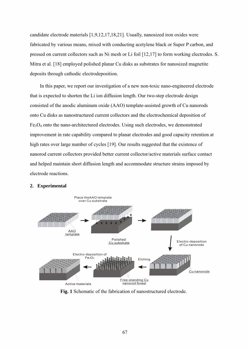
67
candidate electrode materials [1,9,12,17,18,21]. Usually, nanosized iron oxides were
fabricated by various means, mixed with conducting acetylene black or Super P carbon, and
pressed on current collectors such as Ni mesh or Li foil [12,17] to form working electrodes. S.
Mitra et al. [18] employed polished planar Cu disks as substrates for nanosized magnetite
deposits through cathodic electrodeposition.
In this paper, we report our investigation of a new non-toxic nano-engineered electrode
that is expected to shorten the Li ion diffusion length. Our two-step electrode design
consisted of the anodic aluminum oxide (AAO) template-assisted growth of Cu nanorods
onto Cu disks as nanostructured current collectors and the electrochemical deposition of
Fe3O4 onto the nano-architectured electrodes. Using such electrodes, we demonstrated
improvement in rate capability compared to planar electrodes and good capacity retention at
high rates over large number of cycles [19]. Our results suggested that the existence of
nanorod current collectors provided better current collector/active materials surface contact
and helped maintain short diffusion length and accommodate structure strains imposed by
electrode reactions.
2. Experimental
Fig. 1 Schematic of the fabrication of nanostructured electrode.

68
Fig. 2 Schematic of the cell for Cu nanorod electrodeposition.
(a)- copper plate, (b)- alumina template, (c)- cellulose membrane (separator), (d)- plastic
plate, (e)- bolt and nut, (f)- copper wire.
The fabrication process of Fe3O4 based Cu-nanostructured electrodes is schematically
shown in Fig. 1. Key steps include (i) mechanical polishing of Cu substrates, (ii) fabrication
of Cu nanorod arrays as current collectors, and (iii) electrochemical deposition of Fe3O4 onto
the nanostructured current collectors. The key steps are described in more detail in the
following sections.
2.1 Fabrication of Cu nanorod arrays as current collectors
Arrays of perpendicular Cu nanorods were fabricated by cathodic electrodeposition using
a two electrode configuration shown in Fig. 2. Two pieces of Cu disks (1.3cm in diameter, from
Yardney Lithion, Inc.) served as the cathode and the anode. Before electrodeposition, the
cathode Cu disk was mechanically polished with 1.0 micron alpha alumina and 0.05 micron
gamma alumina polishing slurries (Buehler micropolish), followed by rinsing with deionized
(DI) water and ultrasonically cleaning in ethanol. Oxide removal was carried out in a dilute
HCl solution (1:9 in vol. ratio with water). The AAO template (Whatman, Anodisc 13, Cat. No:
6809-7023) was 60-μm thick, with a maximum porosity between 25% and 50%, pore size of
200 nm, and a pore density of 1010 cm-2 [20]. A cellulose paper separator (Whatman, Cat. No:
1001042) was soaked with the electrolytic solution containing 100 g L-1 CuSO4·5H2O (Alfa
Aesar), 20 g L-1 (NH4)2SO4 (Alfa Aesar), and 80 mL L-1 Diethylenetriamine (DETA, Alfa
d
d
e
a
a b f c
69
Aesar) [18]. The whole stack was kept under constant pressure by bolts and nuts. A Keithley
Model 228A in a potentiostatic mode served as the power source.
The electrochemical depositions were carried out at 1.2 DC V at room temperature.
After the electrodeposition, the cathodes were immersed in a 2M NaOH solution for 15
minutes to remove the AAO templates and cleaned in the dilute HCl solution to remove the
surface oxides. The as-prepared samples are immediately used for Fe3O4 deposition to
minimize the surface oxidation of the Cu nanorods.
2.2 Electrodeposition of Fe3O4
Fe3O4 was deposited on the Cu disks with Cu nanorod arrays by electrodeposition. The
electrolyte consisted of 2 M NaOH (Alfa Aesar) and 0.09 M Fe2(SO4)3·5H2O (Alfa Aesar)
complexed with 0.1 M tri-ethanol-amine (Acros Organics) at a pH value of 12.3 [18,21,22].
Electrodeposition was carried out in a two-electrode set-up at 1.5 V (DC) and 50˚C. The Cu
disks with Cu nanorods served as the cathode and a graphite sheet served as the anode. After
electrodeposition samples were rinsed with DI water and dried in air. Fe3O4 were also
electrodeposited under the same conditions on mechanically polished planar Cu substrates to
provide control samples.
2.3 Structure analysis and morphology characterization
The as-prepared nanostructured electrodes were examined by X-ray diffraction (XRD)
using a REGAKU CN2182D5 diffractometer and scanning electron microscopy (SEM) using a
JEOL JSM-840 microscope equipped with energy-dispersive X-ray spectroscopy (EDS).
2.4 Electrochemical tests
The electrochemical performance of our nanostructured electrodes was evaluated
initially in coin cells. Coin/pouch half cells were constructed using metallic lithium as the
counter electrodes and the nanostructured electrodes as the anodes under argon atmosphere
inside a glove box. The half cells were cycled galvanostatically at a rate of C/20 and C/10,
with C being defined as the full use of the capacity in 1 h. Full coin cells were fabricated

70
using both the nanostructured electrodes and the control samples as the anodes and the
standard LiNi0.8Co0.2O2 (Yardney Lithion, Inc.) material as the cathodes. The cathodes were
prepared by coating a paste containing 89% LiNi0.8Co0.2O2, 2% Super P, 2% KS-15 graphite,
2% Shawinigan Acetylene Black (SAB), and 5% Kynar in n-methylpyrrolidone (NMP) onto
Al foil. The loading of the cathode material was 0.125 g in-2. Setela of 20 μm in thickness
was used as the separators. The standard electrolyte of 1M LiPF6 (in ethylene carbonate (EC):
dimethyl carbonate (DMC): diethyl carbonate (DEC)/1:1:1 in mass ratio) was used for both
the half-cell and full-cell tests. The open circuit voltages of the fresh full cells were about 220
mV. The coin cells were cycled under constant current conditions at different rates in the
range of 1/10C to 10C. The charge/discharge capacities and the capacity retention property of
the anodes at different charge/discharge current densities were studied.
3. Results and discussion
3.1 Nanostructured Cu current collector fabrication
Cu nanorods were electrodeposited on the surface of the mechanically polished Cu disks
through the pores of an AAO template. This template-assisted deposition approach offers
multiple advantages. For example, it is convenient to obtain uniform and free-standing Cu
nanorod arrays. In addition, the deposition is cost-efficient, easy to control, and easy to scale
up.
The uniformity in height of the deposited Cu nanorod arrays is expected to be of critical
importance to the performance of the nanostructured electrode. It is significantly affected by
the flatness of the Cu substrates. Atomic force microscope (AFM) study confirmed that
mechanical polishing efficiently reduced the surface roughness of Cu foil. The measured area
root mean square (RMS) roughness decreased from the original 83.0 nm to 16.3 nm after
polishing, which helped to ensure an intimate contact between the cathode Cu disks and the
AAO templates under mechanical pressure and to obtain an even current distribution on the
electrodes during electrodeposition.
The use of the porous cellulose separator soaked with the electrolytic solution provided
a media for Cu ions to transfer from the anode to the cathode uniformly, which helped the Cu
nanorods grow at the similar speed. Since the use of porous cellulose separator eliminated
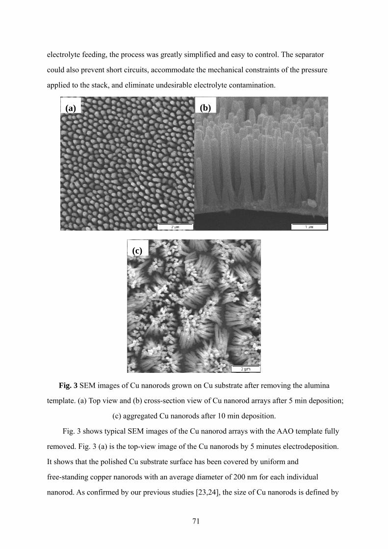
71
electrolyte feeding, the process was greatly simplified and easy to control. The separator
could also prevent short circuits, accommodate the mechanical constraints of the pressure
applied to the stack, and eliminate undesirable electrolyte contamination.
Fig. 3 SEM images of Cu nanorods grown on Cu substrate after removing the alumina
template. (a) Top view and (b) cross-section view of Cu nanorod arrays after 5 min deposition;
(c) aggregated Cu nanorods after 10 min deposition.
Fig. 3 shows typical SEM images of the Cu nanorod arrays with the AAO template fully
removed. Fig. 3 (a) is the top-view image of the Cu nanorods by 5 minutes electrodeposition.
It shows that the polished Cu substrate surface has been covered by uniform and
free-standing copper nanorods with an average diameter of 200 nm for each individual
nanorod. As confirmed by our previous studies [23,24], the size of Cu nanorods is defined by
(b)(a)
(c)

72
the pore size of the AAO template. Fig. 3 (b) is the SEM images of the cross-section. In Fig.
3 (b), we can see that the nanorods are perpendicular to the substrate, their lengths are around
2 μm, and the inter-rod distance is less than 100 nm. The Cu nanorods tend to aggregate when
the aspect ratio becomes large. For example, under the present deposition conditions, the
nanorods began to aggregate when the deposition time was longer than 10 minutes as shown
in Fig. 3 (c). Aggregation is detrimental to the subsequent loading of Fe3O4 because Fe3O4
particles tend to crystallize over the top of the Cu nanorod bundles instead of on the surface
of individual Cu nanorods and lose the advantages provided by the nanostructrued current
collectors.
3.2 Electrodeposition of Fe3O4
Fig. 4 XRD pattern of Fe3O4-Cu nanostructured electrode, star: metallic Cu, parallelogram:
Fe3O4 deposit.
Fig. 4 is a typical XRD pattern from the as-prepared nanostructured electrodes. The two
strong peaks at around 43.3˚ and 50.5˚ correspond to the Cu (111) and the Cu (200)
reflections (International Centre for Diffraction Data card No. 04-0836), originating from the
Cu substrate and the Cu nanorods. The Cu (200) reflection is much stronger than that of Cu
(111), suggesting that the Cu substrate and the Cu nanorods are [100] textured. The three
weak reflections can be assigned to (311), (222), and (400) of magnetite Fe3O4 phase (ICDD
No.26-1136), with the (400) reflection the strongest. This indicates that the Fe3O4
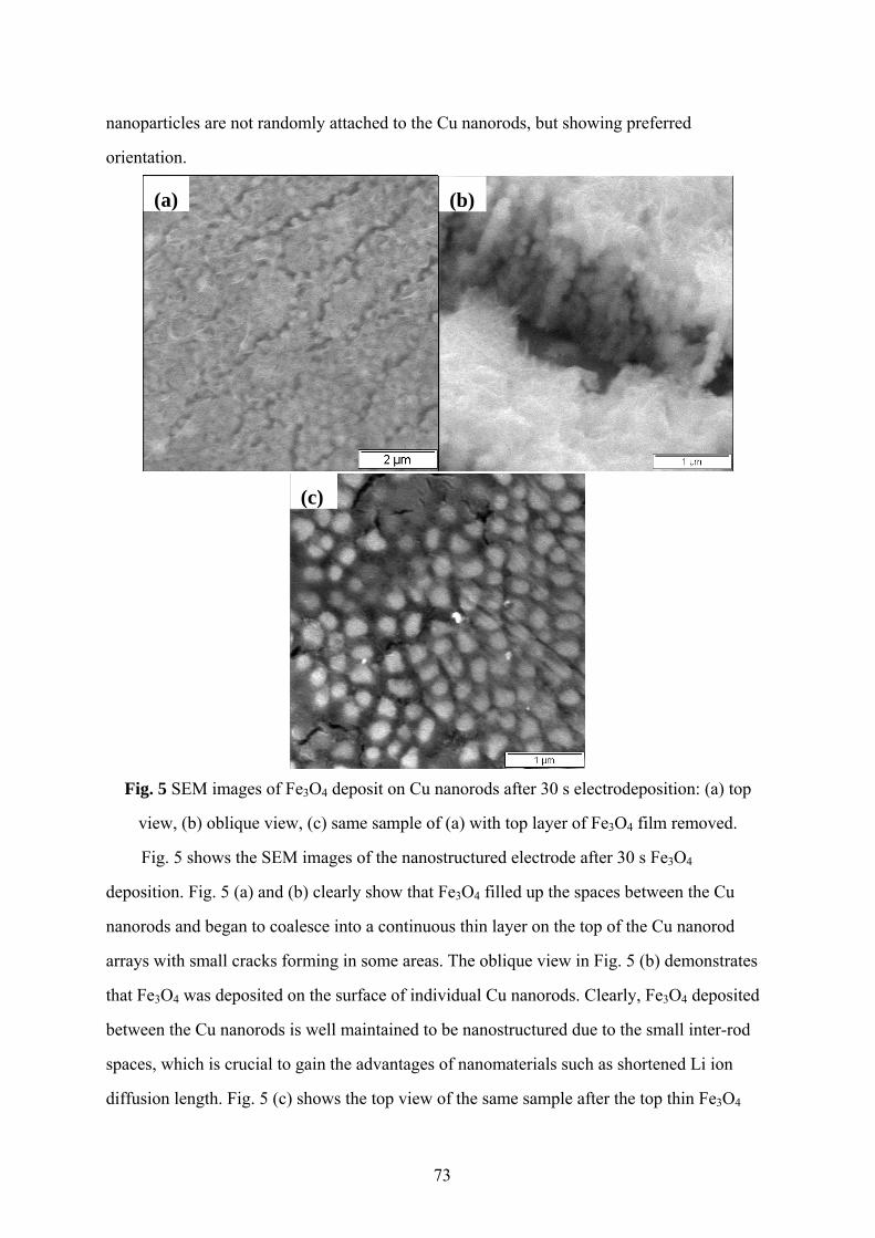
73
nanoparticles are not randomly attached to the Cu nanorods, but showing preferred
orientation.
Fig. 5 SEM images of Fe3O4 deposit on Cu nanorods after 30 s electrodeposition: (a) top
view, (b) oblique view, (c) same sample of (a) with top layer of Fe3O4 film removed.
Fig. 5 shows the SEM images of the nanostructured electrode after 30 s Fe3O4
deposition. Fig. 5 (a) and (b) clearly show that Fe3O4 filled up the spaces between the Cu
nanorods and began to coalesce into a continuous thin layer on the top of the Cu nanorod
arrays with small cracks forming in some areas. The oblique view in Fig. 5 (b) demonstrates
that Fe3O4 was deposited on the surface of individual Cu nanorods. Clearly, Fe3O4 deposited
between the Cu nanorods is well maintained to be nanostructured due to the small inter-rod
spaces, which is crucial to gain the advantages of nanomaterials such as shortened Li ion
diffusion length. Fig. 5 (c) shows the top view of the same sample after the top thin Fe3O4
(b)(a)
(c)

74
layer was carefully removed by polishing. It confirms that the Fe3O4 has been deposited into
the Cu nanorod array. The corresponding EDX spectrum (not shown) verifies the presence of
the elements of Fe, O, and Cu in the area of Fig. 5 (c).
Fig. 6 SEM images of Fe3O4 nanoestructured electrode after electrodeposition for (a) 60 s
and (b) 300 s, inset: higher magnification image of (b).
When the deposition time was increased to 60 s, the Fe3O4 film became thick and bulky
islands with average size around 10 μm with large cracks were evident as shown in Fig. 6 (a).
One possible reason for the crack generation is the different volume change of Fe3O4 deposit
and Cu nanorod arrays during sample drying. Fig. 6 (b) indicates that long deposition time of
300 s led to the formation of even thicker and bigger Fe3O4 islands with size up to tens of
micrometers. The inset shows that the big islands formed right above the small islands in Fig.
6 (a). These micron-sized Fe3O4 islands are undesirable for nanostructured electrodes because
they may block the passage of electrolyte and Li ion and prevent us from taking the
advantages provided by Cu nanorod currently collectors.
3.3 Pouch/coin cell cycling tests
(a) (b)
10 μm

75
Fig. 7 Full coin cells charge capacity vs. cycle number. The cells cycled at different rates
between C/10 and C. For both electrodes, the Fe3O4 electrodeposition time was 120 s. Note
that the geometrical surface area of the copper disk was 1.26 cm2.
The full coin cells were cycled at various constant current rates. Fig. 7 compares the
charge capacities of the coin cells with the nanostructured and the planar control electrodes at
current rates between C/10 and C. For comparison, Fe3O4 electrodeposition conditions were
kept the same and a 120 s deposition time was used for both samples. The cell with the
nanostructured Fe3O4 electrodes demonstrated better rate capabilities at high current rates,
though they exhibited similar capacities at low current rate of C/10 compared with planar
Fe3O4. Fig. 7 stresses the benefit of having a nanostructured current collector compared to a
planar one in terms of power density.

76
Fig. 8 Potential-capacity profiles of the as-prepared nanostructured electrodes with different
Fe3O4 deposition time galvanostatically cycled versus Li at a rate of C/20 for the first cycle
and C/10 for the second and the third. Note that the geometrical surface area of the copper
disk was 1.26 cm2.
The half-cell test results of the nanostructured electrodes with Fe3O4 deposition
durations of 30 s, 120 s and 300 s are presented in Fig. 8. It shows that all the nanostructured
electrodes behaved alike during the first several cycles, demonstrating the characteristic
electrochemical signature of the conversion reactions involved in transition-metal oxide
during charging and discharging [1,21]. The potential dropped rapidly to reach a well-defined
plateau below 1 V corresponding to the full reduction of Fe3O4 into the Fe0/Li2O mixture [21].
On cycling, the common charge/discharge hysteretic profiles which are inherent to
conversion reactions were maintained. The sample with 300 s Fe3O4 deposition time
exhibited the largest capacity compared to the other three, which is expected since longer
deposition promises more active materials. Fig. 8 also shows that the capacity retention of
electrodes with longer deposition durations, i.e. 120 s and 300 s, deteriorated faster than those
with shorter deposition time, i.e. 30 s, which is consistent with Tarascon’s work [18,21]. The
electrode Coulombic efficiency is higher for electrodes with a short Fe3O4 deposition time. A
value of 88% was obtained after 3 cycles for a deposition time of 30 s, compared to 80% after
300 s of electrodeposition.

77
Fig. 9 The capacity retention of a Fe3O4 film electrodeposited onto nanostructured copper
substrate for different time and cycled at a variety of rates. Inset: SEM image of the electrode
with 30 sec Fe3O4 deposition after cycling tests.
Fig. 9 shows the charge/discharge capacity profiles of the nanostructured electrodes with
different Fe3O4 deposition time cycled at various current rates. It is notable that the capacity
of the electrode with 30 s Fe3O4 deposit demonstrated the best sustained reversible capacity
through out the whole cycling process, indicating the electrochemical and mechanical
robustness of the electrode. SEM observation after cycling tests revealed no significant
morphology change of either the Fe3O4 deposits or the Cu nanorods (inset in Fig. 9). In
contrast, the capacities of the electrode with 5-min Fe3O4 deposition dropped fastest with
increasing cycle numbers and those of the electrode with 2-min deposition dropped
intermediately.
These half-cell test results, combined with the observation in Fig. 6, strongly suggest
that as the time for Fe3O4 deposition elapses and the polycrystalline Fe3O4 particles aggregate
into micron-sized islands above the Cu nanorod arrays, these islands tend to block the access
of electrolyte to the inter-nanorod spaces, cause loss of the advantages of nanostructured
material, and are undesirable for capacity retention during charge/discharge cycling.
0.0
0.5
1.0
1.5
2.0
2.5
0 2 4 6 8 10 12 14Cycle No
Dis
char
ge /
Cha
rge
Cap
acity
(mA
h)JG-N15-BS1.036 JG-N15-BS1.036JG-N15-BS2.037 JG-N15-BS2.037JG-N15-BS3.038 JG-N15-BS3.038
5 min
2 min
30 sec
5 min
2 min
30 sec
30 sec2 min5 min
8 C
2C
C
C/2
500 nm
78
4. Conclusions
The current work develops a nanostructured anode material for Li-ion battery by a
two-step fabrication process. This process consists of the AAO template-assisted growth of
Cu nanorods onto Cu substrates as nanostructured current collectors followed by the Fe3O4
electrodeposition. Uniform and free-standing Cu nanorod arrays were deposited onto
mechanically polished Cu disks and the active material of Fe3O4 was successfully grown on
the surface of individual Cu nanorods. The nanostructured electrode showed superior rate
capabilities compared to the planar control samples. It was also observed that the formation
of micron-sized Fe3O4 islands led to deteriorated reversible capacity retention.
Acknowledgement
The financial support for this work from NASA (contract No. NNJ07JB33C) &
OSD/ONR (contract No N00014-07-M-0110; 07PR06126-00) are gratefully acknowledged.
We thank Prof. Robert Thompson for his help during this work. The authors also want to
thank Prof. Nancy Burnham for her help in AFM analysis.
References
[1] P. Poizot, S. Laruelle, S. Grugeon, L. Dupont, J. M. Tarascon, Nature 407 (2000) 496-499.
[2] N. Li, C. R. Martin, B. Scrosati, J. Power Sources 97-98 (2001) 240-243.
[3] X. He, W. Pu, L. Wang, J. Ren, C. Jiang, C. Wan, Electrochimica Acta 11 (2007)
3651-3653.
[4] V. Subramanian, A. Karki, K. I. Gnanasekar, F. Eddy, B. Rambabu, J. Power Sources 159
(2006) 186-192.
[5] H. Wang, T. Abe, S. Maruyama, Y. Iriyama, Z. Ogumi, K. Yoshikawa, Adv. Mater. 17 (2005)
2857-2860.
[6] M. Park, Y. Kang, G. Wang, S. Dou, H. Liu, Adv. Func. Mater. 18 (2008) 455-461.
[7] J. Li, Z. Tang, Z. Zhang, Electrochem. Commun. 7 (2005) 62-67.
[8] P. G. Bruce, Chem. Commun. 19 (1997) 1817-1824.
[9] E. Hosono, S. Fujihara, I. Honma, M. Ichihara, H. Zhou, J. Electrochem. Soc. 153 (2006) A
1273-A1278.
[10] A. S. Arico, P. Bruce, B. Scrosati, J. M. Tarascon, W.V. Schalkwijk, Nature Mater. 4 (2005)
366-377.

79
[11] C. R. Sides, N. Li, C. J. Patrissi, B. Scrosati, C. R. Martin, MRS Bull. 26 (2002) 604-608.
[12] S. Ito, K. Nakaoka, M. Kawamura, K. Ui, K. Fujimoto, N. Koura, J. Power Sources 146
(2005) 319-322.
[13] A. R. Armstrong, G. Armstrong, J. Canales, R. Garacia, P. G. Bruce, Adv. Mater. 17 (2005)
862-865.
[14] J. M. D. Coey, A. E. Berkowitz, Li. Balcells, F. F. Putris, F. T. Parker, Appl. Phys. Lett. 72
(1998) 734-736.
[15] M. M. Thackeray, W. I. F. David, J. B. Goodenough, Mater, Res. Bull. 17 (1982) 785-793.
[16] M. M. Thackeray, J. Coetzer, Mater, Res. Bull. 16 (1981) 591-597.
[17] D. Larcher, C. Masquelier, D. Bonnin, Y. Chabre, V. Masson, J. B. Leriche, J. M. Tarascon,
J. Electrochem. Soc. 150 (2003) A133-A139.
[18] S. Mitra, P. Poizot, A. Finke, J. M. Tarascon, Adv. Funt. Mater. 16 (2006) 2281-2287.
[19] J. S. Gnanaraj, J. F. DiCarlo, H. Duan, J. Liang, R. W. Thompson, 10th Power Source
R&D Symposium, Williamsburg, VA, August 20-23, 2007.
[20] http://www.whatman.com
[21] P. L. Taberna, S. Mitra, P. Poizot, J. M. Tarascon, Nature Mater. 5 (2006) 567-573.
[22] H. M. Kothari, E. A. Kulp, S. J. Limmer, P. Poizot, E. W. Bohannan, J. A. Switzer, J. Mater.
Res. 21 (2006) 293-301.
[23] H. Chik, J. Liang, S. G. Cloutier, N. Koukli, J. M. Xu, Appl. Phys. Lett. 84 (2004)
3376-3378.
[24] J. Liang, H. Chik, J. Xu, IEEE J. Selected Topics in Quantum Electronics 8 (2002)
998-1008.
80
CHAPTER IV: RESEARCH CONCLUSIONS AND FUTURE WORK
This thesis presents a series of experimental investigations covering the synthesis, integration,
and characterization of functional nanomaterials. Corresponding to the research objectives in
Chapter I, the following conclusions are drawn. Future work is also included at the end of
each conclusion.
1. AAO template assisted nanofabrication [Paper # 1 and Appendix A]: based on a
two-step anodization process to prepare AAO templates, we fabricated a variety of ordered
1-D nanostructures including metal NWs, metal NRs and CNTs of different sizes, aspect ratio,
and shapes. The metal NWs and NRs are synthesized using both DC and AC
electrodeposition, and the CNTs are obtained by CVD with and without metallic catalysts.
Morphology study shows that the dimension of the as-prepared 1-D nanostructures is well
defined by nanochannel of the template which can be further controlled by adjusting the
anodization conditions such as voltage, time, and electrolyte bath. Among them, the
Y-junction Co NWs and Y-junction Cu NWs synthesized by AC electrodeposition are the first
example of using AC electrodeposition to fabricate Y-junction metal NWs. By structural
analysis, it’s interesting to find that Co NWs is a mixture of FCC and HCP structures,
whereas FCC microstructure is retained for Cu NWs.
Further work includes (1) using HRTEM to study in more details the microstructure near
the junction; (2) identifying the factors affecting the Co NWs by varying synthesis conditions
such as pH value of electrolyte bath, voltage, frequency; (3) studying the effect of
introduction of Y-junction on the mechanical property and thermal property of the metal
NWs.
2. Synthesis and study of the hierarchical structures of CNFs and CMFs or GMFs [Paper
# 2]: employing the CCVD technique, the possibility of growing CNFs on individual CFs and
GFs to form a three-dimensional hierarchical structure is explored. CNFs grown on both CFs
and GFs demonstrated coexistence of two types of morphology. One is winded fibers
implying frequent orientation change. The other one is relatively straight and long fiber with
graphene sheets parallel to each other. Possible reasons causing varying deposition and

81
precipitation rates for different catalyst surfaces include: (1) different catalytic ability for
different crystal planes, (2) asymmetrical shaped catalyst particles which lead to different
diffusion path lengths for the carbon atoms to traverse; (3) nonuniform carbon supply. CNFs
grown on CMF substrate are thicker and more uniform than those on GMF substrates
probably due to different catalyst-substrate interaction and different growth temperature. The
as-grown three-dimensional carbon-carbon and carbon-glass hierarchical structures provide
an effective means to connect nanoscale entities to the higher hierarchy.
Further work includes: (1) optimizing the synthesis conditions to produce the CNF and
CMF or GMF hierarchical structures; (2) controlling the growth direction of the CNFs on
MFs by external forces such as electric field and magnetic field; and (3) synthesis
hierarchical structures of other materials such as ZnO.
3. Design and study of the electrochemical property of nanostructured electrodes [Paper
# 3, # 4, and Appendix B]: both Fe3O4-based and TiO2-based nanostructured electrodes are
developed by a two-step fabrication process. This process consists of the AAO
template-assisted growth of Cu nanorods onto Cu substrates as nanostructured current
collectors followed by the loading of Fe3O4 or TiO2. Uniform and free-standing Cu nanorod
arrays are deposited onto mechanically polished Cu disks and the active material of Fe3O4 or
TiO2 is successfully grown on the surface of individual Cu nanorods. The active materials are
also deposited on planar Cu substrate for comparison. The Fe3O4-based nanostructured
electrode shows superior rate capabilities compared to the planar control samples. It is also
observed that the formation of micron-sized Fe3O4 islands led to deteriorated reversible
capacity retention. While for TiO2-based nanostructured electrode, though large amount of
TiO2 is deposited and high specific capacity is gained with the introduction of Cu nanorods,
higher degree of oxidation also occurs for the nanostructured electrodes in comparison of the
planar electrodes, which affects Li ion insertion mechanism and the rate capability.
Further work includes: for Fe3O4-based electrode, (1) scaling up the fabrication process
to make large rectangular electrodes ( "" 64 × ) instead of small circle ones (Φ 13 mm) to
move toward pilot testing; (2) More detailed microstructure study by SAD or XRD to clarify
the Li ion insertion/deinsertion process; (3) for TiO2-based electrode, stabilizing the

82
fabrication process and reducing the oxidation of Cu NR during fabrication.
83
APPENDIX A: AAO-ASSISTED FABRICATION OF 1 D
NANOMATERIALS
1. AAO template synthesis
Based upon the information presented in Chapter II, anodized aluminum oxide (AAO)
template-assisted fabrication provides an important strategy to synthesize nanomaterials.
The synthesis of AAO templates with densely hexagonally packed straight nanochannels is a
good starting point for this method. The nanopores self-organize into a highly ordered array
of uniform pores with the pore diameter, the period, and the array size being variable over
ranges that are beyond the reach of standard e-beam lithography [1-4]. The alumina nanopore
array is formed by anodization of high-purity aluminum under certain carefully controlled
anodization conditions. The optimized anodization parameters in different electrolytes are
shown in Table A.1. Periodical porous oxide with remarkably ordered arrangements of
cylindrical pores, whose diameter varies in the range of 35 nm to 300 nm, can now be
realized routinely in our lab using a two-step process published previously [5-7].
Table A.1 Optimized parameters for AAO template anodization [8]
Electrolyte
(acid) Concentration
Temperature
(oC)
Voltage
(V)
Typical resulting
mean diameter (nm)
Oxalic 0.3 M 10 40 45
Phosphoric 1 M 0 160 400
Sulfuric 0.5 M 0 25 30

84
Fig. A.1 SEM images of AAO template during a two-step process in oxalic acid system: (a)
after 1st anodization; (b) after dissolving the membrane formed in the 1st anodization; (c) top
view and (d) cross-section view of the membrane after 2nd anodization. Scale bars: (a) and (b)
1 μm, (c) and (d) 100 nm.
Fig. A.1 shows SEM images of the AAO template in each step of the two-step
fabrication process in an oxalic acid system. From Fig. A.1a, we can see that during the 1st
anodization, porous anodic alumina forms at the aluminum surface. A hexagonal topographic
structure is exposed on the Al substrate after dissolving the alumina film formed in the 1st
anodization (Fig. A.1b). The nanochannels grow from the structure during the 2nd anodization
and as a result the arrangement of the nanopore array mimics the hexagonal topographic
structure (Fig. A .1c and d). The resultant nanoscale pores are parallel, straight, and oriented
vertical to the surface (Fig. A.1e) and they are uniform in diameter (approximately 45 nm)
and in spacing.

85
2. AAO-template assisted nanofabrication
As shown in Fig. A.2, by using the AAO membrane as a template, a number of different
nanostructures including metal nanowire (NW) arrays, metal nanorod (NR) arrays and carbon
nanotube (CNT) arrays have been synthesized.
Fig. A.2 Schematic of the fabrication of ordered inorganic nanomaterial arrays: (a) metal NW
arrays electrodeposited in AAO template; (b) metal NW array embedded in AAO template
with tips exposed by etching; (c) CNT array grown by CCVD; (d) Y-shaped CNT array grown
by CCVD.
2.1 Carbon nanotubes fabricated by AAO-assisted CVD method
2.1.1 CNTs synthesized by catalytically CVD
Fig. A.3 shows SEM images of CNTs synthesized using the fabrication process
described in one of the published paper [9]. As shown in Fig. A.3a, the template is covered by
a layer of junk carbon which is a by-product of CNT growth. After thermal cleaning in air at
600 oC for 30 min, this layer of junk carbon can be removed and the hexagonal pattern of
nanochannels underneath is shown in Fig. A.3b. The CNTs can be exposed by dry etching the
AAO template (Fig. A.3c). It was found that a high filling rate is obtained under current
conditions. Fig. A.3d shows that the CNTs are well embedded in the nanochannels. Fig. A.3e

86
and 3f indicate that the Co catalysts stay at the bottom part of the AAO template during CNT
growth.
Fig. A.3 CNTs fabricated by AAO-assisted CCVD method: (a) as-prepared samples; (b)
samples after thermal cleaning at 600 oC for 30 min; (c) CNTs with tips exposed by reactive
ion etching (TIE); (d) cross-section view of CNTs embedded in the AAO nanochannels; (e)
and (f) cross-section view and the corresponding element mapping (Co) of the bottom part of
the sample. Scale bars: (a), (b), (c), and (d) 100 nm, (e) and (f) 3 μm.
As shown in Fig. A.4, the outer diameter is 44.96 + 3.79 nm and the inner diameter is
11.80 + 2.24 nm. Clearly, the outer diameter is close to the pore size of the AAO template.
Higher magnification TEM images show that both hollow (Fig. A.4b) and bamboo-like CNTs
(Fig. A.4c) can be observed in a single nanotube.
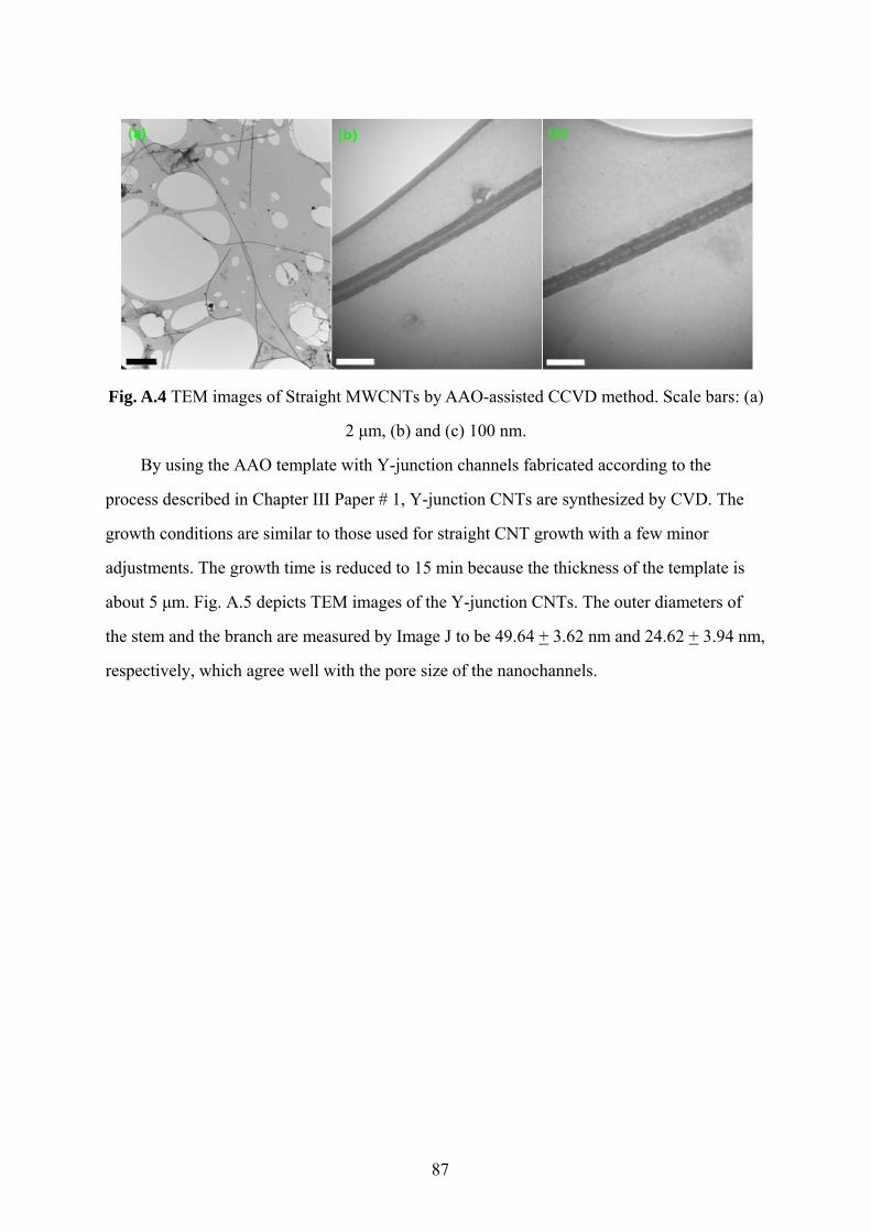
87
Fig. A.4 TEM images of Straight MWCNTs by AAO-assisted CCVD method. Scale bars: (a)
2 μm, (b) and (c) 100 nm.
By using the AAO template with Y-junction channels fabricated according to the
process described in Chapter III Paper # 1, Y-junction CNTs are synthesized by CVD. The
growth conditions are similar to those used for straight CNT growth with a few minor
adjustments. The growth time is reduced to 15 min because the thickness of the template is
about 5 μm. Fig. A.5 depicts TEM images of the Y-junction CNTs. The outer diameters of
the stem and the branch are measured by Image J to be 49.64 + 3.62 nm and 24.62 + 3.94 nm,
respectively, which agree well with the pore size of the nanochannels.
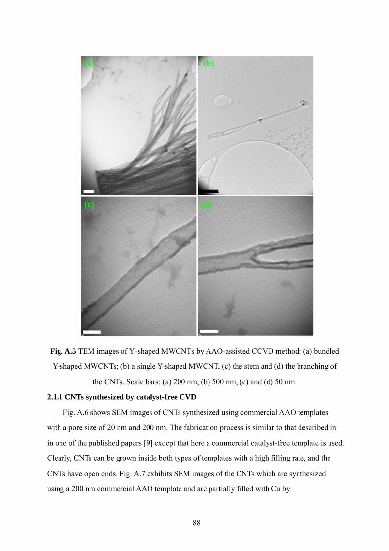
88
Fig. A.5 TEM images of Y-shaped MWCNTs by AAO-assisted CCVD method: (a) bundled
Y-shaped MWCNTs; (b) a single Y-shaped MWCNT, (c) the stem and (d) the branching of
the CNTs. Scale bars: (a) 200 nm, (b) 500 nm, (c) and (d) 50 nm.
2.1.1 CNTs synthesized by catalyst-free CVD
Fig. A.6 shows SEM images of CNTs synthesized using commercial AAO templates
with a pore size of 20 nm and 200 nm. The fabrication process is similar to that described in
in one of the published papers [9] except that here a commercial catalyst-free template is used.
Clearly, CNTs can be grown inside both types of templates with a high filling rate, and the
CNTs have open ends. Fig. A.7 exhibits SEM images of the CNTs which are synthesized
using a 200 nm commercial AAO template and are partially filled with Cu by

89
electrodeposition. Cu rods with length about 1 um are deposited inside the CNTs, which is
confirmed by the EDS.
Fig. A.6 CNT fabricated by CVD using commercial AAO templates with pore size of (a), (b)
20nm and (c), (d) 200nm. Scale bars: (a) and (d) 100 nm, (b) and (c) 1 μm.
Fig. A.7 (a), (b) SEM images of CNTs partially filled with Cu and (c) Cu element mapping of
area (b). Scale bars: (a) 100 nm, (b) and (c) 2 μm.
Fig. A.8 shows CNTs synthesized using homemade AAO templates. The template is
separated from an Al substrate by 1 wt.% HgCl2 solution, and then is subject to CNT growth
at 600 oC without using any catalyst. The CNTs can easily be grown inside the template with
dimension well confined by the nanochannels. The TEM image (Fig. A.8d) has less contrast
compared to that of CNTs grown with Co catalysts (Fig. A.4b), which suggests poorer
crystallinity of CNTs when a catalyst is not used.

90
Fig. A.8 Homemade 60nm AAO template: (a), (b) cross-section view of CNTs in the AAO
template; (c), (d) TEM images of the CNTs. Scale bars: (a) 10 μm, (b) 1μm, (c) 500 nm, and
(d) 50 nm.
2.2 Co nanowires fabricated by AAO-assisted method
Fig. A.9 shows SEM images of Co NWs synthesized by the AC electrodeposition
process described in Chapter III Paper # 1. As we can see from Fig. A.9a and b, Co NWs with
diameter of 45.64 + 9.12 nm are obtained, and the dimensions of the Co NW is defined by the
nanochannels in the AAO template. TEM images shown in Fig. A.9c and d illustrate that a
thin layer of oxide is formed on the surface of a single NW.
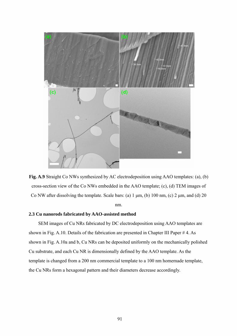
91
Fig. A.9 Straight Co NWs synthesized by AC electrodeposition using AAO templates: (a), (b)
cross-section view of the Co NWs embedded in the AAO template; (c), (d) TEM images of
Co NW after dissolving the template. Scale bars: (a) 1 μm, (b) 100 nm, (c) 2 μm, and (d) 20
nm.
2.3 Cu nanorods fabricated by AAO-assisted method
SEM images of Cu NRs fabricated by DC electrodeposition using AAO templates are
shown in Fig. A.10. Details of the fabrication are presented in Chapter III Paper # 4. As
shown in Fig. A.10a and b, Cu NRs can be deposited uniformly on the mechanically polished
Cu substrate, and each Cu NR is dimensionally defined by the AAO template. As the
template is changed from a 200 nm commercial template to a 100 nm homemade template,
the Cu NRs form a hexagonal pattern and their diameters decrease accordingly.

92
Fig. A.10 Cu NRs synthesized by electrodeposition using (a), (b) commercial AAO template
and (c), (d) homemade AAO template. Scale bars: (a) 10 μm, (b) 1 μm, (c) 100 nm, and (d) 1
μm.
Reference
[1] Li, J.; Papadopoulos, C.; Xu, J. M. Appl. Phys. Lett. 1999, 75, 367. [2] Parthasarathy, R. V.; Phani, K. L. N.; Martin, C. R. Adv. Mater. 1995, 7, 896.
[3] Kyotani, T.; Tsai, L.; Tomita, A. Chem. Mater. 1996, 8, 2109.
[4] Li, J.; Moskovits, M.; Haslett, T. L. Chem. Mater. 1998, 10, 1963.
[5] Liang, J.; Chik, H.; Yin, A.; Xu, J. M. J. Appl. Phys. 2002, 91, 2544.
[6] Liang, J.; Chik, H.; Xu, J. M. IEEE J. Sel. Top. Quantum Electron 2002, 8, 998.
[7] Li, J.; Papadopoulos, C.; Xu, J. M.; Moskovits, M. Appl. Phys. Lett. 1999, 75, 367.
[8] Liang, J. Non-lithographic fabrication of Superlattices for Nanometric
electro-magnetic-optic applications. Ph. D. dissertation. 2005.
[9] Pradhan, N. R.; Duan, H.; Liang, J.; Iannacchione, G. S. In press by Nanotechnology.

93
APPENDIX B: ELECTROCHEMICAL PREPARATION OF
NANOSTRUCTURED TiO2 AS ANODE MATERIAL FOR Li ION
BATTERIES
(published in Proc. MRS 2008, Boston, MA, )
ABSTRACT
TiO2 is an attractive anode material for Li-ion batteries due to its high capacity, high
mechanical stability during Li intercalation/deintercalation process, limited side reactions
with the electrolyte, low cost, and environmental friendliness. In this study, titanium
hydroxide gel films were prepared in acidic aqueous solutions of TiOSO4, H2O2 and KNO3
by potentiostatic cathodic electrosynthesis on various copper substrates, including planar Cu
foil, mechanically polished planar Cu foil, and Cu nanorod arrays grown on Cu foil.
Crystalline TiO2 films were obtained by heat treating the electrodeposited titanium hydroxide
gel films at 500 oC in argon atmosphere. The morphology and microstructure of the TiO2
films were characterized by scanning electron microscope (SEM) and X-ray diffraction
(XRD). SEM results showed that after deposition, each Cu nanorod has been covered by a
layer of TiO2 gel, forming a core-shell structure. The effects of Cu nanorod arrays on the
morphology and the electrochemical property of the TiO2 deposits were discussed.
INTRODUCTION
Lithium-ion (Li-ion) batteries are attractive candidates for use as power storage in
many applications because of their high specific energy, energy density and cycle life. The
conventional Li-ion batteries have achieved great commercial success since their invention in
1980’s. However, they have been suffering from two major problems. Firstly, when the
charge/discharge rate is higher than 1 C (C defined as the full use of the capacity in 1 h) or Li
ions are inserted into graphite at a potential of less than 1 V versus Li+/Li, lithium may be
plated on the carbon electrode surface causing safety hazard [1]. Secondly, slow solid-state
diffusion of Li+ within the electrode materials limits the rate capability of Li-ion batteries

94
[2,3]. Therefore there is a vigorous research effort on using nanomaterials to improve the
safety and the rate capabilities of electrodes.
TiO2 is a promising anode material for next-generation Li ion batteries. Various
nanoforms of TiO2, including nanocrystalline anatase, amorphous TiO2 and TiO2 nanotubes,
have been studied as high-rate Li-ion anode materials and indeed demonstrated improved
property at high current densities [4-9]. Of the various polymorphs of TiO2, anatase,
amorphous or unique nanostructured TiO2 is desirable for fast and high volume lithium
insertion/desertion. It has also been shown that not only the particle size of the active
materials making up the electrode but also the size of grains within these particles plays
critical roles in the Li+ insertion/deinsertion process [10]. However, it is not easy to control
the size and size distribution of the nanoparticles or clusters. In addition, packing the
nanomaterials into an electrode film with good electrical contact and sufficient mechanical
support while retain the large accessible surface area to electrolyte and small diffusion length
of Li+ is critical to the electrochemical properties of the electrode. Therefore, not only low
cost and highly controllable synthesis of nanomaterials, but also a smart design of
nanostructured electrode exploring the full gain offered by using nanomaterials is demanded.
In this work, based on the same philosophy that we used to fabricate Fe3O4-based Cu
nanostructured electrode [11], we propose to develop a novel nanoengineered TiO2 anode
with rapid Li+ recharge characteristics. The morphology and electrochemical properties of the
nanoengineered electrode will be compared to its planar counterparts.
EXPERIMENT
Electrode fabrication
The fabrication process of TiO2 based Cu-nanostructured electrodes, as shown in Fig. 1,
is similar to the process described in one of our previous publications [11,12]. Briefly, key
steps include (i) mechanical polishing of Cu substrates, (ii) fabrication of Cu nanorod (NR)
arrays as current collectors by anodized aluminum oxide (AAO) templates assisted
electrodeposition, and (iii) electrochemical deposition of TiO2 onto the nanostructured current
collectors. Before electrodeposition, the cathode Cu disk was mechanically polished,
followed by rinsing with deionized (DI) water and ultrasonically cleaning in ethanol.
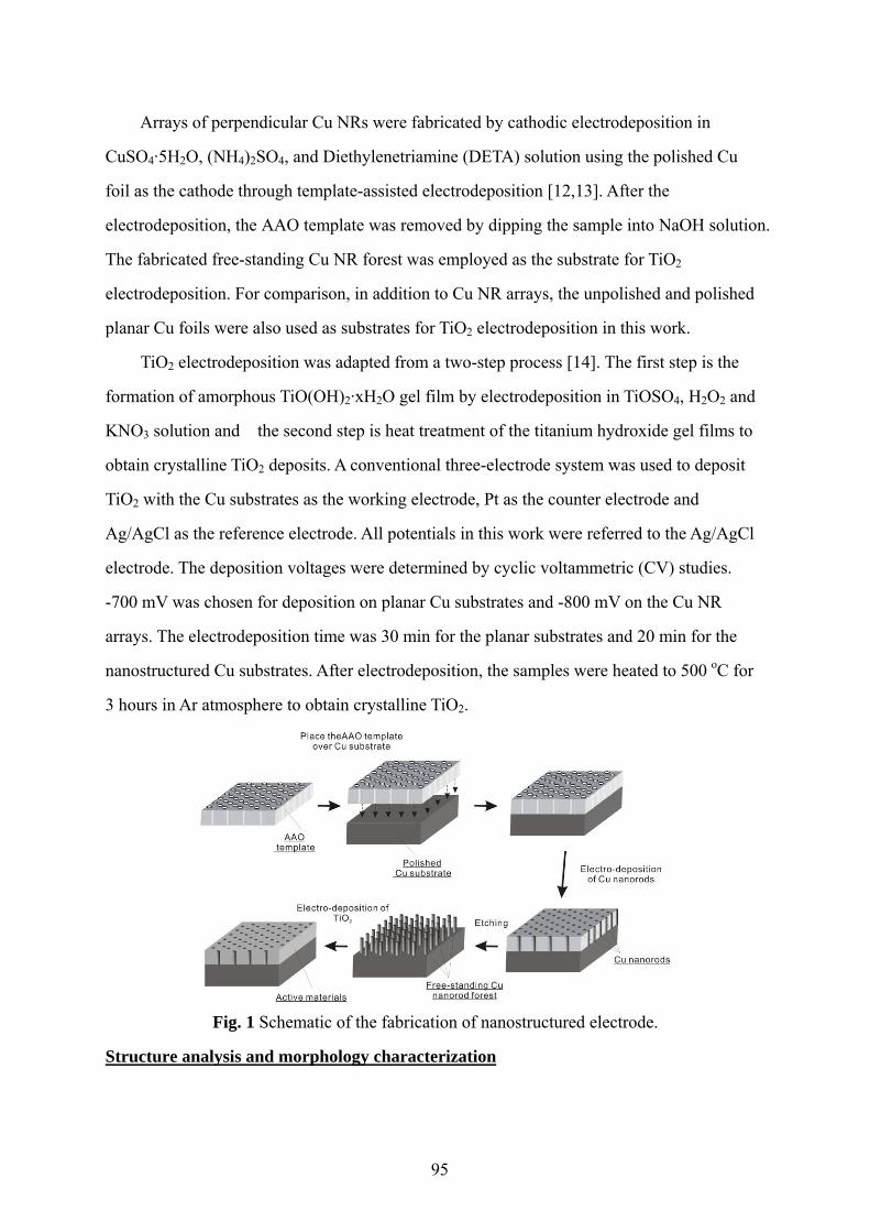
95
Arrays of perpendicular Cu NRs were fabricated by cathodic electrodeposition in
CuSO4·5H2O, (NH4)2SO4, and Diethylenetriamine (DETA) solution using the polished Cu
foil as the cathode through template-assisted electrodeposition [12,13]. After the
electrodeposition, the AAO template was removed by dipping the sample into NaOH solution.
The fabricated free-standing Cu NR forest was employed as the substrate for TiO2
electrodeposition. For comparison, in addition to Cu NR arrays, the unpolished and polished
planar Cu foils were also used as substrates for TiO2 electrodeposition in this work.
TiO2 electrodeposition was adapted from a two-step process [14]. The first step is the
formation of amorphous TiO(OH)2·xH2O gel film by electrodeposition in TiOSO4, H2O2 and
KNO3 solution and the second step is heat treatment of the titanium hydroxide gel films to
obtain crystalline TiO2 deposits. A conventional three-electrode system was used to deposit
TiO2 with the Cu substrates as the working electrode, Pt as the counter electrode and
Ag/AgCl as the reference electrode. All potentials in this work were referred to the Ag/AgCl
electrode. The deposition voltages were determined by cyclic voltammetric (CV) studies.
-700 mV was chosen for deposition on planar Cu substrates and -800 mV on the Cu NR
arrays. The electrodeposition time was 30 min for the planar substrates and 20 min for the
nanostructured Cu substrates. After electrodeposition, the samples were heated to 500 oC for
3 hours in Ar atmosphere to obtain crystalline TiO2.
Fig. 1 Schematic of the fabrication of nanostructured electrode.
Structure analysis and morphology characterization
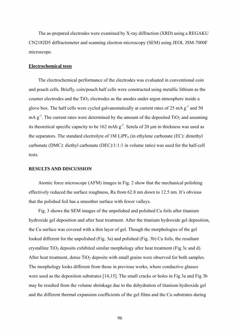
96
The as-prepared electrodes were examined by X-ray diffraction (XRD) using a REGAKU
CN2182D5 diffractometer and scanning electron microscopy (SEM) using JEOL JSM-7000F
microscope.
Electrochemical tests
The electrochemical performance of the electrodes was evaluated in conventional coin
and pouch cells. Briefly, coin/pouch half cells were constructed using metallic lithium as the
counter electrodes and the TiO2 electrodes as the anodes under argon atmosphere inside a
glove box. The half cells were cycled galvanostatically at current rates of 25 mA g-1 and 50
mA g-1. The current rates were determined by the amount of the deposited TiO2 and assuming
its theoretical specific capacity to be 162 mAh g-1. Setela of 20 μm in thickness was used as
the separators. The standard electrolyte of 1M LiPF6 (in ethylene carbonate (EC): dimethyl
carbonate (DMC): diethyl carbonate (DEC)/1:1:1 in volume ratio) was used for the half-cell
tests.
RESULTS AND DISCUSSION
Atomic force microscope (AFM) images in Fig. 2 show that the mechanical polishing
effectively reduced the surface roughness, Ra from 62.8 nm down to 12.5 nm. It’s obvious
that the polished foil has a smoother surface with fewer valleys.
Fig. 3 shows the SEM images of the unpolished and polished Cu foils after titanium
hydroxide gel deposition and after heat treatment. After the titanium hydroxide gel deposition,
the Cu surface was covered with a thin layer of gel. Though the morphologies of the gel
looked different for the unpolished (Fig. 3a) and polished (Fig. 3b) Cu foils, the resultant
crystalline TiO2 deposits exhibited similar morphology after heat treatment (Fig 3c and d).
After heat treatment, dense TiO2 deposits with small grains were observed for both samples.
The morphology looks different from those in previous works, where conductive glasses
were used as the deposition substrates [14,15]. The small cracks or holes in Fig 3a and Fig 3b
may be resulted from the volume shrinkage due to the dehydration of titanium hydroxide gel
and the different thermal expansion coefficients of the gel films and the Cu substrates during

97
drying the sample, which is common for oxide deposited on metal substrates [16-18].
Fig. 2 AFM images of unpolished (a) and polished Cu foils (b).
Fig. 3 SEM images of unpolished and polished Cu foil after (a) (b) titanium hydroxide gel
deposition, and after heat treatment (c) (d). Scale bars: (a) - (d) 1 μm.
Typical SEM images of the electrode using Cu NR arrays as the current collector are
shown in Fig. 4. Fig. 4a and b are the top-view and oblique-view SEM images of
free-standing Cu NR arrays obtained by the template assisted electrodeposition. The top-view
image (Fig.4a) shows that the polished Cu substrate surface has been covered by uniform and
free-standing copper nanorods. As confirmed by our previous studies [19,20], the size of Cu
(a) (b)
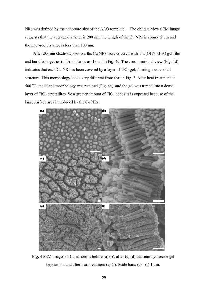
98
NRs was defined by the nanopore size of the AAO template. The oblique-view SEM image
suggests that the average diameter is 200 nm, the length of the Cu NRs is around 2 μm and
the inter-rod distance is less than 100 nm.
After 20-min electrodeposition, the Cu NRs were covered with TiO(OH)2·xH2O gel film
and bundled together to form islands as shown in Fig. 4c. The cross-sectional view (Fig. 4d)
indicates that each Cu NR has been covered by a layer of TiO2 gel, forming a core-shell
structure. This morphology looks very different from that in Fig. 3. After heat treatment at
500 oC, the island morphology was retained (Fig. 4e), and the gel was turned into a dense
layer of TiO2 crystallites. So a greater amount of TiO2 deposits is expected because of the
large surface area introduced by the Cu NRs.
Fig. 4 SEM images of Cu nanorods before (a) (b), after (c) (d) titanium hydroxide gel
deposition, and after heat treatment (e) (f). Scale bars: (a) - (f) 1 μm.

99
XRD was used to characterize the microstructure of the as-fabricated electrodes. Fig. 5
displays typical XRD patterns of TiO2 deposited on polished Cu foil and on Cu NR arrays.
The XRD pattern of Cu foil without TiO2 deposits is also presented for comparison. Fig. 5
suggests that for (b) and (c), in addition to the Cu peaks from the substrate and TiO2 peaks
from the TiO2 deposits, there are also peaks for the phase of Cu2O which probably formed
during the heat treatment. Moreover, the intensities of the TiO2 peaks near 25.29 and 48.05
increased when the substrate was changed from polished Cu foil to the Cu NR arrays, which
implies greater load of TiO2 for the nanostructured electrode. While the intensities of the
Cu2O peaks near 29.56, 36.42, 42.30, and 61.35 were negligible for planar Cu foil with TiO2
deposits, suggesting minimal oxidation of the sample during heat treatment.
Fig. 5 XRD patterns for TiO2-based electrodes: Cu foil without TiO2 deposition (a), polished
planar Cu foil with TiO2 deposits (b), and Cu NR arrays with TiO2 deposits (c). Note: sphere
– TiO2, square – Cu2O, triangle – Cu.
The capacity and rate capability of the electrode were tested by galvanostatic
charge/discharge tests. Fig. 6 displays the initial discharge curves of the nanostructured and
planar electrode with unpolished Cu foil at the current rate of 25 mA g-1. Both samples give
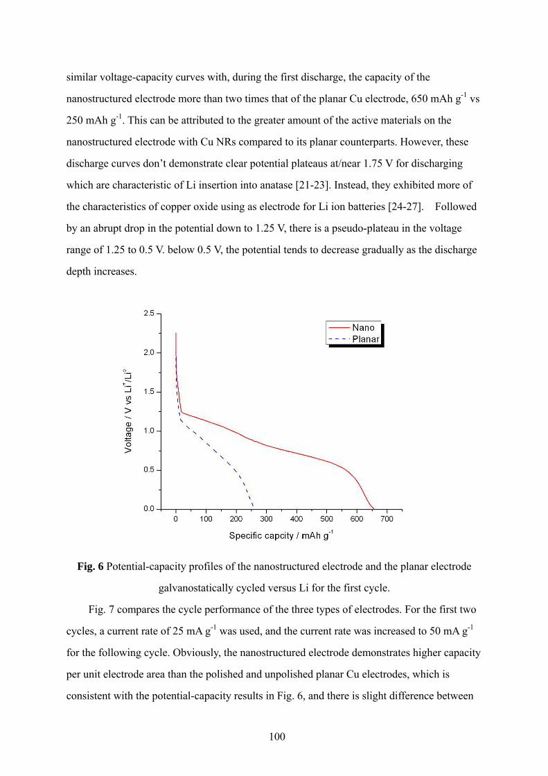
100
similar voltage-capacity curves with, during the first discharge, the capacity of the
nanostructured electrode more than two times that of the planar Cu electrode, 650 mAh g-1 vs
250 mAh g-1. This can be attributed to the greater amount of the active materials on the
nanostructured electrode with Cu NRs compared to its planar counterparts. However, these
discharge curves don’t demonstrate clear potential plateaus at/near 1.75 V for discharging
which are characteristic of Li insertion into anatase [21-23]. Instead, they exhibited more of
the characteristics of copper oxide using as electrode for Li ion batteries [24-27]. Followed
by an abrupt drop in the potential down to 1.25 V, there is a pseudo-plateau in the voltage
range of 1.25 to 0.5 V. below 0.5 V, the potential tends to decrease gradually as the discharge
depth increases.
Fig. 6 Potential-capacity profiles of the nanostructured electrode and the planar electrode
galvanostatically cycled versus Li for the first cycle.
Fig. 7 compares the cycle performance of the three types of electrodes. For the first two
cycles, a current rate of 25 mA g-1 was used, and the current rate was increased to 50 mA g-1
for the following cycle. Obviously, the nanostructured electrode demonstrates higher capacity
per unit electrode area than the polished and unpolished planar Cu electrodes, which is
consistent with the potential-capacity results in Fig. 6, and there is slight difference between

101
the latter two in terms of capacity. Fig. 7 also shows that all the capacity decayed fast with the
cycling, which is not expected for an anatase-based electrode for Li ion batteries. [21,28,29]
For the nanostrucutred electrode in particular, its capacity decays from 350 mAh g-1 on the
first cycle to 184 mAh g-1 on the second one and to about 100 mAh g-1 on the eighth cycle.
Clearly, the introduction of copper oxide in the heat treatment is affecting the rate capability
of the electrodes. More work is in progress to optimize the nanostructured electrodes to
improve the rate capability and test the electrode life time through large number of cycle
tests.
Fig. 7 Comparison of the cycle performance of TiO2-based electrodes on different substrates.
CONCLUSIONS
A novel design of TiO2-based nanoengineered electrodes for Li ion batteries was
proposed. The nanostructured electrodes were manufactured by adopting two-step process
consisting of the template-assisted growth of Cu nanorods onto Cu foils as nanostructured
current collectors and the electrodeposition of TiO2. The TiO2 was also deposited on polished
and unpolished planar Cu substrates for comparison. SEM results show that each of the Cu

102
nanorod has been covered with a dense layer of TiO2 thin film. XRD is used to confirm the
crystalline TiO2 phase and the XRD results show that larger amount of TiO2 was deposited
with the introduction of Cu nanorods, which is favorable to gain a high specific capacity.
However, higher degree of oxidation was also occurred for the nanostructured electrodes,
which will affect Li ion insertion mechanism and the rate capability.
ACKNOWLEDGMENTS
The authors are grateful to Prof. Nancy A. Burnham at WPI for the access of the AFM
facility.
REFERENCES
[1] P.G. Bruce, B. Scrosati, and J.M. Tarascon, Angew. Chem. Int. Ed. 47, 2930 (2008).
[2] J. Li, Z. Tang, and Z. Zhang, Electrochem. Comm. 7, 62 (2005).
[3] P.G. Bruce, Chem. Commun. 19, 1817 (1997).
[4] V. Subramanian, A. Karki, K.I. Gnanasekar, F.P. Eddy and B. Rambabu, J. Power Sources
159, 186 (2006).
[5] M. Hibino, K. Abe, M. Mochizuki and M. Miyayama, J. Power Sources 126, 139 (2004).
[6] M. Wagemaker, A.P.M. Kentgens and F.M. Mulder, Nature 418, 397 (2002).
[7] Y.K. Zhou, L. Cao, F. B. Zhang and H.L. Li, J. Electrochemical Society 150, A1246 (2003).
[8] A. Guerfi, P. Charest, K. Kinoshita, M. Perrier and K. Zaghib, J. Power Sources 126, 163
(2004).
[9] A.R. Armstrong, G. Armstrong, J. Canales and P.G. Bruce, J. Power Sources 146, 501
(2005).
[10] J.O. Besenhard, J. Yang, and M. Winter, J. Power Sources 68, 87 (1997).
[11] H. Duan, J. Gnanaraj, X. Chen, B. Li, and J. Liang, J. Power Sources 185, 512 (2008).
[12] J.S. Gnanaraj, J.F. DiCarlo, H. Duan, J. Liang, R.W. Thompson, 10th Power Source R&D
Symposium, Williamsburg, VA, 2007.
[13] X. Chen, H. Duan, Z. Zhou, J. Liang, J. Gnanaraj, Nanotechnology 19, 365306 (2008).
[14] S. Karuppuchamy, K. Nonomura, T. Yoshida, T. Sugiura, and H. Minoura, Solid State
Ionics 151, 19 (2002).
[15] B.R. Sankapal, S.D Sartale, M.C. Lux-Steiner, and A. Ennaoui, C.R. Chimie 9, 702
(2006).
[16] J. Georgieva, S. Armyanov, E. Valova, I. Poulios, S. Sotiropoulos, Electrochem. Acta. 51,

103
2076 (2006).
[17] I. Zhitomirski, L. Gal-Or, A. Khon and M.D. Spang, J. Mater. Sci. 32, 803 (1997).
[18] I. Zhitomirski and L. Gal-Or, J. Eur. Ceram. Soc. 16, 819 (1996).
[19] J. Liang, H. Chik, and J. Xu, IEEE J. Sel. Top. Quantum Electron. 8, 998 (2002).
[20] H. Chik, J. Liang, S.G. Cloutier, N. Koukli, and J.M. Xu, Appl. Phys. Lett. 84, 3376
(2004).
[21] X. Gao, H. Zhu, G. Pan, S. Ye, Y. Lan, F. Wu, and D. Song. J. Phys. Chem. B 108, 2868
(2004).
[22] S.Y. Huang, L. Kavan, I. Exnar and M. Gratzel, J. Electrochem. Soc. 142, L142 (1995).
[23] F. Bonino, L. Busani, M. Lazzari, M. Manstretta, B. Rivolta and B.Scrosati, J. Power
Sources 6, 261 (1981).
[24] S. Grugeon, S. Laruelle, R. Herrera-Urbina, L. Dupont, P. Poizot, and J-M. Tarascon, J.
Electrochem. Soc. 148, A285 (2001).
[25] J. Morales, L. Sanchez, F. Martin, J.R. Ramos-Barrado and M. Sanchez. Thin Solid
Films 474, 133 (2005).
[26] X. P. Gao, J. L. Bao, G. L. Pan, H. Y. Zhu, P. X. Huang, F. Wu and D. Y. Song. J. Phys.
Chem. B 108, 5547 (2004).
[27] X. Zhang, D. Zhang, X. Ni, J. Song and H. Zheng. J. Nanopart. Res. 10, 839 (2008).
[28] H. Furukawa, M. Hibino and I. Honma. J. Electrochem. Soc. 151, A527 (2004).
[29] V. Subramanian, A. Karki, K.I. Gnanasekar, F.P. Eddy and B. Rambabu. J. Power
Sources 159, 186 (2006).
Related Documents