Accepted Manuscript Title: Synthesis and characterization of CuInS 2 nanostructure by Ultrasonic-assisted method and different precursors Authors: Mehdi Mousavi-Kamazani, Masoud Salavati-Niasari, Hamid Emadi PII: S0025-5408(12)00615-0 DOI: doi:10.1016/j.materresbull.2012.08.044 Reference: MRB 6044 To appear in: MRB Received date: 5-3-2012 Revised date: 14-8-2012 Accepted date: 17-8-2012 Please cite this article as: M. Mousavi-Kamazani, M. Salavati-Niasari, H. Emadi, Synthesis and characterization of CuInS 2 nanostructure by Ultrasonic- assisted method and different precursors, Materials Research Bulletin (2010), doi:10.1016/j.materresbull.2012.08.044 This is a PDF file of an unedited manuscript that has been accepted for publication. As a service to our customers we are providing this early version of the manuscript. The manuscript will undergo copyediting, typesetting, and review of the resulting proof before it is published in its final form. Please note that during the production process errors may be discovered which could affect the content, and all legal disclaimers that apply to the journal pertain.

Welcome message from author
This document is posted to help you gain knowledge. Please leave a comment to let me know what you think about it! Share it to your friends and learn new things together.
Transcript
Accepted Manuscript
Title: Synthesis and characterization of CuInS2 nanostructureby Ultrasonic-assisted method and different precursors
Authors: Mehdi Mousavi-Kamazani, MasoudSalavati-Niasari, Hamid Emadi
PII: S0025-5408(12)00615-0DOI: doi:10.1016/j.materresbull.2012.08.044Reference: MRB 6044
To appear in: MRB
Received date: 5-3-2012Revised date: 14-8-2012Accepted date: 17-8-2012
Please cite this article as: M. Mousavi-Kamazani, M. Salavati-Niasari, H.Emadi, Synthesis and characterization of CuInS2 nanostructure by Ultrasonic-assisted method and different precursors, Materials Research Bulletin (2010),doi:10.1016/j.materresbull.2012.08.044
This is a PDF file of an unedited manuscript that has been accepted for publication.As a service to our customers we are providing this early version of the manuscript.The manuscript will undergo copyediting, typesetting, and review of the resulting proofbefore it is published in its final form. Please note that during the production processerrors may be discovered which could affect the content, and all legal disclaimers thatapply to the journal pertain.
Page 1 of 33
Accep
ted
Man
uscr
ipt
1
Synthesis and characterization of CuInS2 nanostructure by Ultrasonic-assisted
method and different precursors
Mehdi Mousavi-Kamazani a, Masoud Salavati-Niasari *
, a, b
, Hamid Emadi c
a Institute of Nano Science and Nano Technology, University of Kashan, Kashan, P. O. Box. 87317-51167,
I. R. Iran.
b Department of Inorganic Chemistry, Faculty of Chemistry, University of Kashan, Kashan, P. O. Box.
87317-51167, I. R. Iran
c School of Chemistry, University College of Science, University of Tehran, Tehran,
I. R. Iran
*Corresponding author: Tel.: +98 361 5555 333, Fax: +98 361 555 29 30.
E-mail address: [email protected] (Masoud Salavati-Niasari).
Abstract
This paper reports on the synthesis of CuInS2 nanostructure via an ultrasonic assisted method by
employing different sulfur source Morphology, structure and composition of the obtained products were
characterized by X-ray diffraction (XRD), energy dispersive X-ray analysis (EDX), scanning electron
microscope (SEM), infrared (IR) spectrum, and photoluminescence (PL) spectroscopy. The effects of
ultrasonic irradiation, power and time of irradiation, surfactant, and type of copper source were
investigated.
Keywords: CuInS2; nanostructure; Ultrasonic; Electron microscopy.
Page 2 of 33
Accep
ted
Man
uscr
ipt
2
1. Introduction:
A solar cell is an electronic device designed for converting the irradiated sunlight into electricity The
simplest way to reach this goal is constructing a p-n homo junction and other structures such as
metal/semiconductor (MS) and hetero junction complex that are still used as solar cells [1]. Chalcopyrite
I-II-VI compounds are the ternary analogs of the binary II-VI compounds and have received much
attention, as they can be used as both n- and p- type [2]. Cu-chalcopyrite semiconductor materials are used
as absorber layers in hetero junction solar cell devices [3]. The chalcopyrite semiconductor CuInS2 (CIS)
is particularly promising, for photovoltaic applications because it has a layer absorption coefficient of
about 10-5
cm-1
and a direct band gap energy of approximately 1.54 eV which is in the optimum range for
solar-energy conversion [4–8]. Hence, various studies have focused on providing a simple and suitable
method for synthesis of CuInS2 nanostructures and so various methods have been applied to synthesize
CuInS2 thin film and powders including molecular single-source precursors [9], solvothermal reactions
[10–16], microemulsion method [17], microwave irradiation [18], surfactant-assisted chemical reactions
[19,20], chemical vapor deposition(CVD) [21], sputtering [22], spray pyrolysis [23], molecular beam
deposition [24], and electrodeposition [25]. These methods produced nanocrystals with different
morphologies such as nanoparticles [26–28], hollow nanospheres [19], nanowires [12], nanorods [10, 11],
pyramidal nanocrystales [13], and porous microspheres [14,15]. Chen et al. have prepared color tunable
CuInS2 nanocrystals which its optical properties is greatly affected by the Cu/In molar ratio [29].
Transparent, flexible and luminescent composite films were prepared by dispersing CuInS2 based quantum
dots into a cyanoethyl cellulose matrix which their color could be regulated over green, yellow, orange,
pink, and red by changing quantum dots content [30]. Pyramidal CuInS2 nanocrystals were synthesized in
gram scale and their size dependent optical properties were investigated [31].
Page 3 of 33
Accep
ted
Man
uscr
ipt
3
In current study we report new method for synthesis of CuInS2 nanostructure. Nano sized CuInS2 were
prepared via an ultrasonic-assisted method. This method was developed to study and control the
morphology of CuInS2 nanostructure by employing different sulfur and copper source. Recently,
sonochmical method has been used since this method is simple, fast, economical, manageable,
environmentally benign and convenient [32–34]. Also influences of different parameters were
investigated.
2. Experimental
2.1. Materials and physical measurements
All chemical reagents in this experiment were of analytical grade and used without further purification.
The precursor complex, [bis(2-hydoxyacetophenato)copper(II)], was prepared as mentioned in literature
[35]. A multiwave ultrasonic generator (Sonicator 3000; Bandeline, MS 72,Germany), equipped with a
converter/transducer and titanium oscillator (horn), 12.5 mm in diameter, operating at 20 kHz with a
maximum power output of 80 W, was used for the ultrasonic irradiation. The ultrasonic generator
automatically adjusted the power level. X-ray diffraction (XRD) patterns were recorded by a Philips-
X’pertpro, X-ray diffractometer using Ni-filtered Cu Kα radiation. Fourier transform infrared (FT-IR)
spectra were recorded on Nicolet Magna-550 spectrometer in KBr pellets. The electronic spectrum of the
sample was taken on Perkin-Elmer LS-55 luminescence spectrometer. Scanning electron microscopy
(SEM) images were obtained on LEO-1455VP equipped with an energy dispersive X-ray spectroscopy.
2.2. Preparation of CIS nanocrystals
Page 4 of 33
Accep
ted
Man
uscr
ipt
4
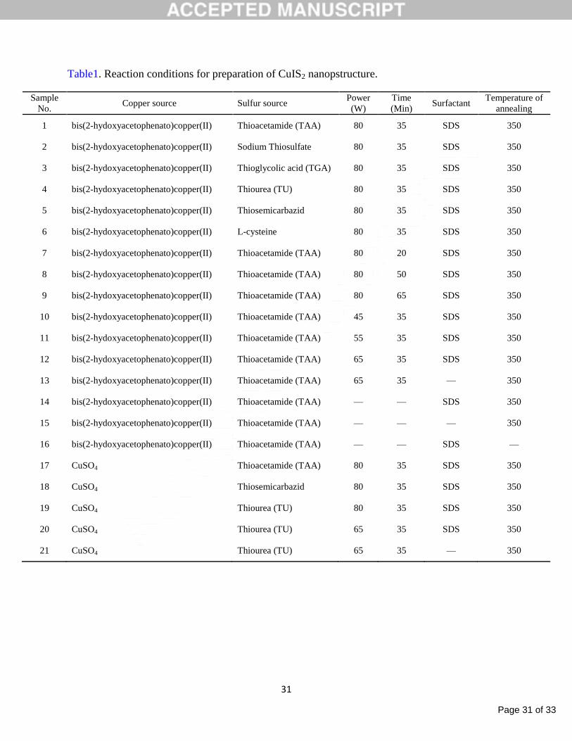
In a typical synthesis procedure [bis(2-hydoxyacetophenato)copper(II)], InCl3, sulfide precursor, and
sodium dodecyl sulfate (SDS) were dissolved in 40 ml of propylene glycol (PG) with the molar ratio of
1:1:2: 1/5. The obtained mixture was stirred and and refluxed (188 °C) for 15 min. Afterward, the solution
was exposed by ultrasonic irradiation with different power at room temperature for appropriate time. The
black precipitates were centrifuged, washed several times with absolute alcohol and distilled water, dried
at 50 °C at vacuum oven for 10 h. The final black products were annealed for 1 h at 350 °C in argon
atmosphere to produce crystalline products [7, 36]. The annealing temperature was selected considering
the thermal stability of the compound [36]. Some parameters including ultrasonic power, reaction time,
sulfide precursor, and etc. were changed for reaching the optimized condition. Also similar experiments
were performed by CuSO4 as copper source and the results were compared with those of obtained by
[bis(2-hydoxyacetophenato)copper(II)]. Reaction conditions are listed in Table 1.
3. Results and discussion:
The crystal structure and phase composition of the annealed and unannealed products were characterized
by powder X-ray diffraction pattern, as shown in Fig.1. Fig.1a shows that before annealing no crystalline
phase was obtained. By annealing at 350 °C for 1 h CuInS2 obtained but samples were composed of In2O3
as impurity (Fig.1b). To remove this impurity samples were annealed again at 350 °C for 1 h but under
Argon atmosphere. It was revealed that under this condition crystalline CuInS2 obtained and no
characteristic peaks of impurities such as CuS, Cu2S, In2S3, and In2O3 were detected (Fig. 1c). All of the
diffraction peaks in Fig.1c can be indexed to the tetragonal structure of CuInS2 (space group I-42d) which
is very close to the values in the literature (JCPDS No. 75-0106 with lattice parameters a = b = 5.5170 A°
c = 11.0600 A°). Acceptable matches are observed for compound indicating the presence of only one
Page 5 of 33
Accep
ted
Man
uscr
ipt
5
crystalline phase in the samples. From broaden peaks in XRD it can be concluded that the particle size of
the product is small. The average crystallite diameter of the obtained product was estimated from Debeys-
Scherrer equation: ; Where β is the breadth of the observed diffraction line at its half-intensity
maximum, K is the so-called shape factor, and λ is the wavelength of X-ray source used in XRD. The
average crystallite diameter of the obtained products was about 16 nm (Sample no. 1). Also it was
revealed by XRD analysis that by using other sulfur source the same products obtained while their
crystallinity and average crystallite diameter were different. These differences can be attributed to the
release rate of sulfide in the reaction medium which affects growth parameters of the crystals. Carful
observation to Fig. 2 clearly shows that when TU and L-cystein were used as sulfide source the
crystallinity of products was lower in comparison with those which obtained with other source of sulfide.
Also the smallest crystalline diameter was observed when TAA was applied as sulfide precursors.
However in all cases CuInS2 was obtained after annealing at 350 °C.
A typical EDX spectrum is shown in Fig.3, which indicates the presence of Cu, In, and S in the
products. Based on the calculation of the peak areas, the ratio of copper to indium, and sulfide was found
to be approximately 1:1:2 as expected. Therefore, both XRD and EDX analyses revealed that pure CuInS2
was successfully synthesized via the current synthetic route.
When chemical composition is concerned, exact determination of the product content has remained
problematic. The accuracy of energy- and wavelength-dispersive X-ray analysis frequently used for this
application is relied on appropriate standards, that has unidentified minor phases and impurities. This
technique shows excellent element selectivity, quantitative character and high surface sensitivity which
can be used without standards to analyze all types of materials. In addition, XP spectra reflect atomic scale
chemical interactions, i.e. the bonds between neighboring atoms, and thus XPS also provides reliable
structural characteristics for nano-crystalline or amorphous composition, for which the application of
Page 6 of 33
Accep
ted
Man
uscr
ipt
6
diffraction techniques is not straightforward. Herein, XPS analysis was applied for further characterization
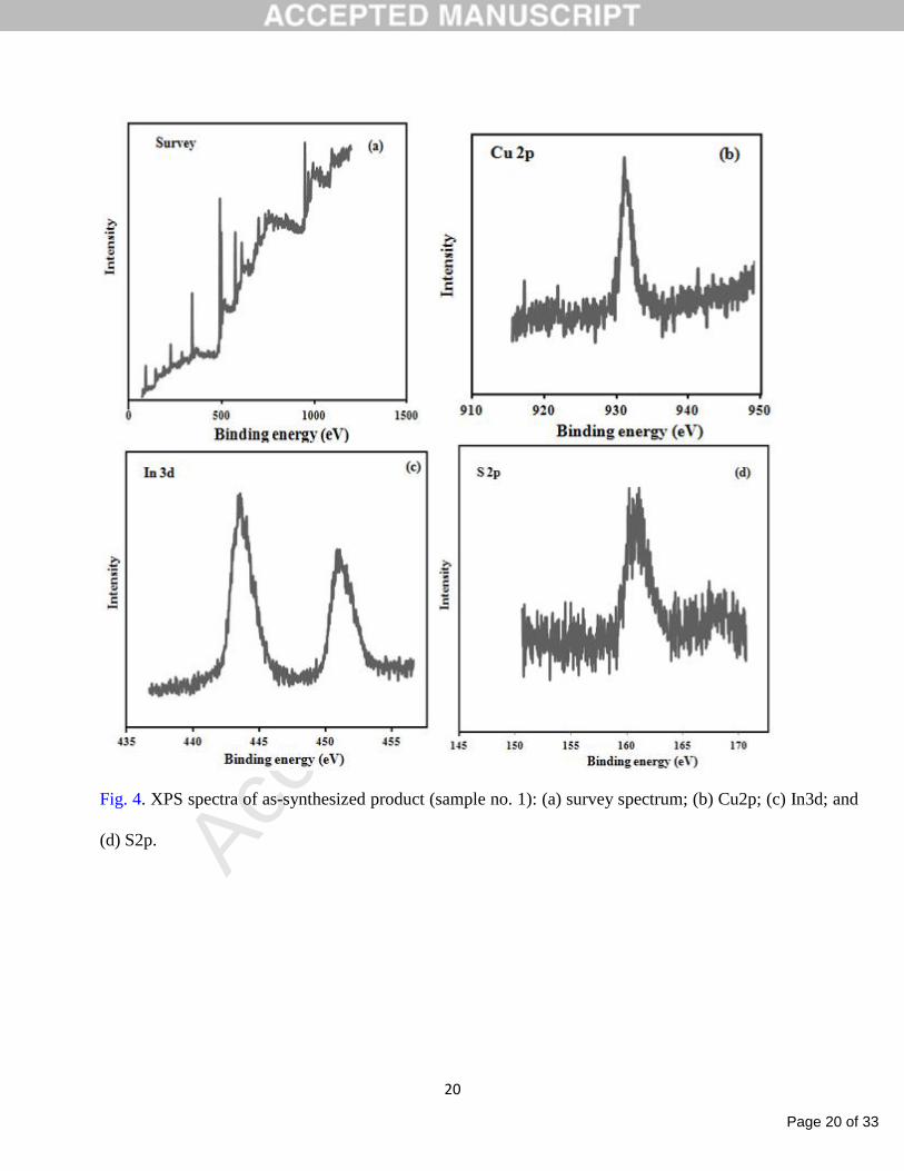
of quality and composition of the as prepared sample. It can be seen in Fig.4 that binding energy of Cu
2p3, In 3d5/2, S 2p are 931.22, 443.58, and 161.16 respectively and there is no impurity in the final
product. The ratio of Cu/In/S was calculated by quantification of the peaks which were 0.96:1:2.02 that
are in good agreement with stoichiometry of CuInS2.
The morphology of the samples was revealed by scanning electron microscopy (SEM). Fig. 5 shows
SEM images of the samples 1-6 obtained by different sulfur source. Based on modern complex theory,
some of them which dissociated and release S-2
also behave as potential ligands. Since the reactivity of
different sulfide source is not the same in the coordination reactions, the CuInS2 nanostructure synthesized
using different sulfide source led to different motphology of the nanostructure [7]. It can be seen that
when TAA and thiosemicarbazid were used as sulfide source, CuInS2 nanoparticles obtained and when TU
was used these particles agglomerated. This difference in size may be due to difference in release rate of
S-2
, when S-2
was released faster, more nucleus of sample were produced at the beginning of the reaction
which had small size that due their high surface energy, they have agglomerated. When sodium thiosulfate
was used, rice shape nanostructures obtained (Fig. 5b). Thioglycolic acid as complexing agent has
significant effect in formation of nanorods (Fig. 5c). It can prevent CuS nanocrystal aggregation and at
appropriate condition can form complex with Cu2+
which turns to CuS clusters [37] and finally changes to
CuInS2 after annealing. L-cysteine has several functional groups such as –NH2, –COOH, and –SH. When
excess concentration of L-cysteine was used, it absorbed on the surface of CuS nanoparticles and
hydrogen bonds and S-S bonds formed between L-cysteine molecules. The CuS nanoparticles cross-link
via hydrogen bonds and S-S bond interactions and agglomerated which finally turned to CuIS2 after
annealing (Fig. 5f).
Page 7 of 33
Accep
ted
Man
uscr
ipt
7
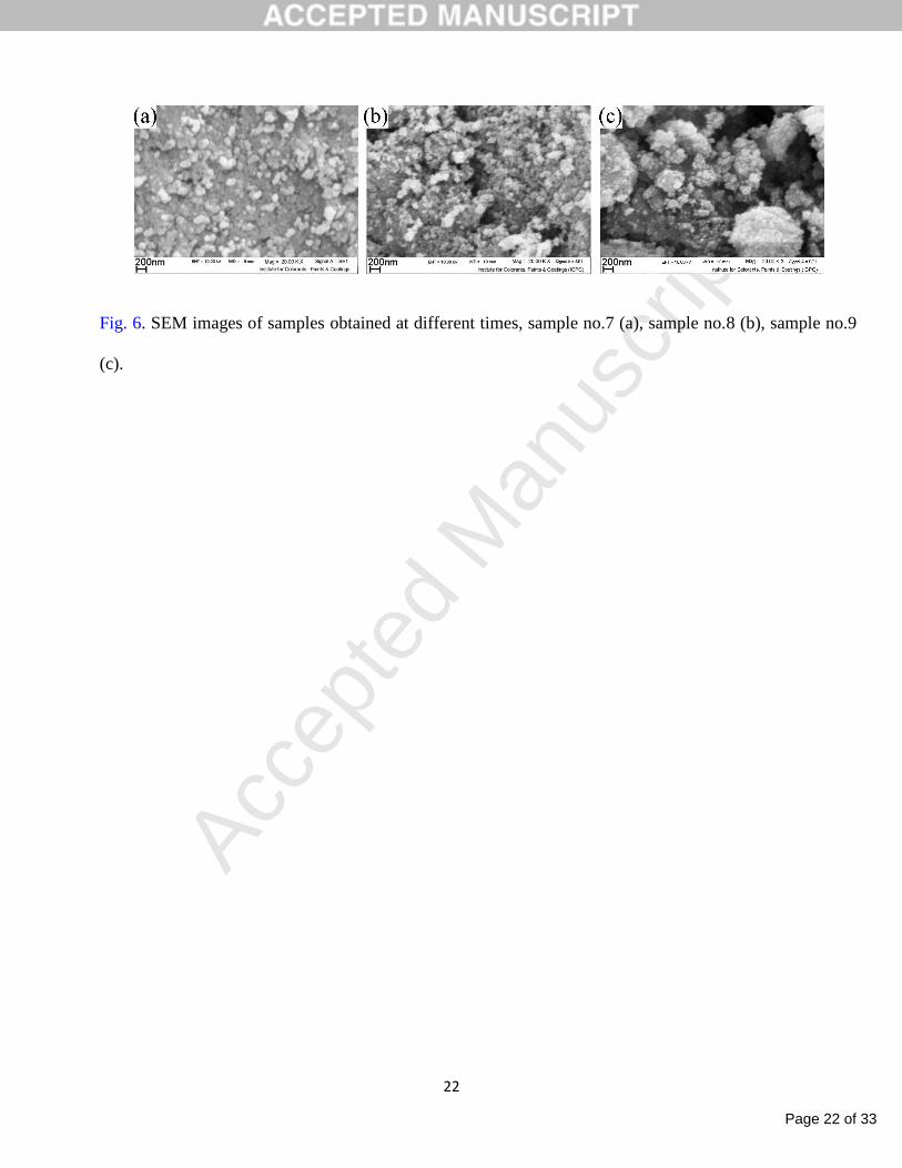
Fig. 6 relates to the SEM images of samples 7, 8, and 9 that were prepared in different times including
20, 50, and 65 min respectively. At 20 min, particles were not separated well and obtained particles were
bigger than those which obtained at higher sonication times (Fig. 6a). With increasing of time to 35 and 55
min small particles obtained (Fig. 5a and 6b respectievly). When reaction time increased to 65 min
agglomeration occurred (Fig. 6c). At this condition small nucleus obtained but when particles become
small consumedly, they are unstable and for more fixity stick together. Thus there is an optimize time
which was 35 min for current experiment.
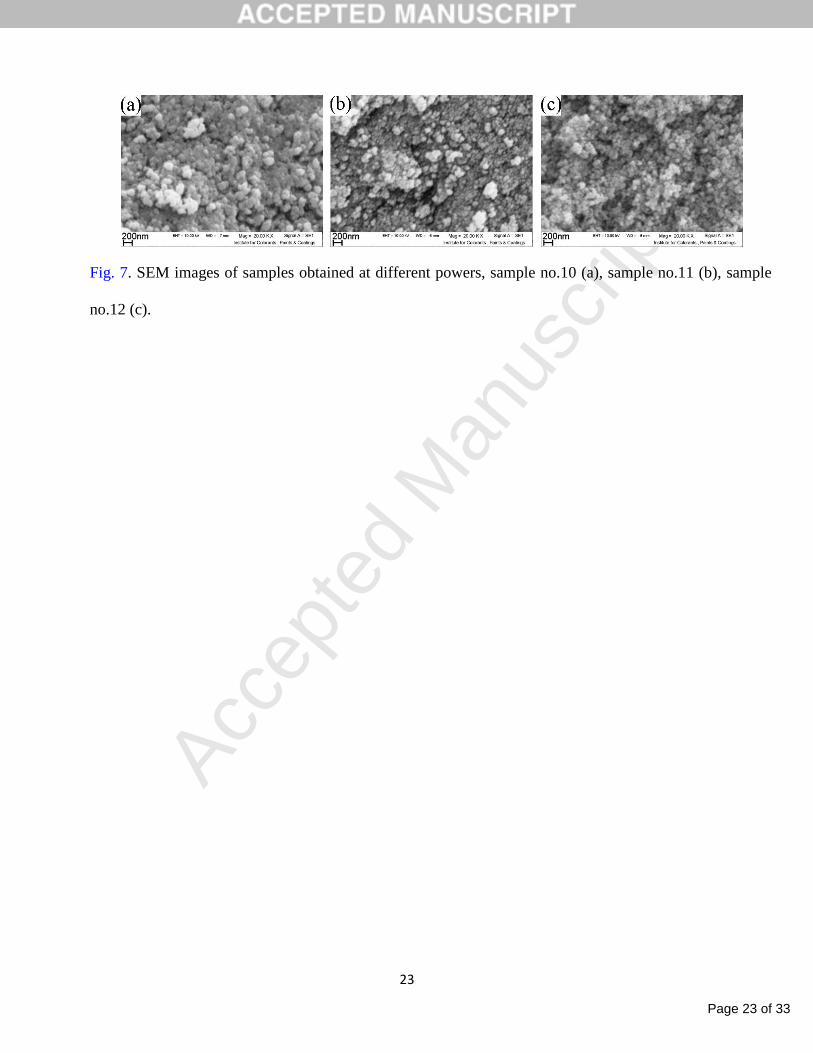
Fig. 7 shows the SEM images of samples 10-12 obtained at different power. In the powers of fewer than
45 W microparticle are observed because they are not separated well and this power is not enough for
them to be separated (Fig. 7a). When power increased to 55 W nanoparticles obtained but samples were
not homogenous well while at power 65 W these samples were separated well and homogenous (Fig. 7b
and Fig. 7c respectively). When power reached to 80 W, effects of agglomeration observed (Fig. 5a).
There is an optimum power for these experiments which is 65 W because in this power nanoparticles
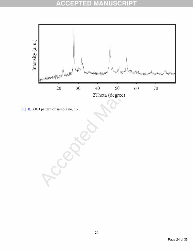
showed better uniformity. XRD pattern (Fig. 8) of samples obtained without ultrasonic irradiation (sample
no. 15) revealed the presence of some impurity such as CuS and In(OH)3 in the final products which
confirm this fact that ultrasonic irradiation is necessary for obtaining CuInS2 nanostructures.
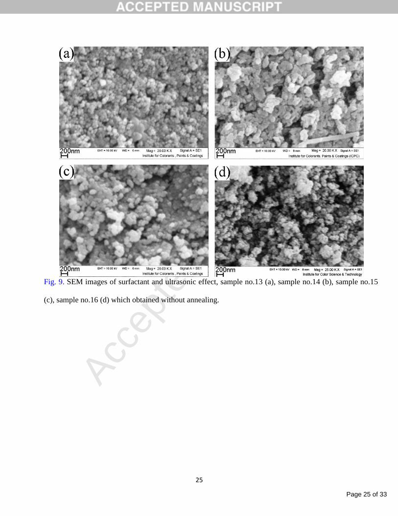
Fig. 9 shows the SEM images of the samples 13-16 that are related to the effect of surfactant and
ultrasonic irradiation. Careful observation to Fig. 7c and Fig. 9a which are related to samples 12 and 13
respectively suggests that the SDS may has role in controlling the size distribution of CuInS2 particle.
With no surfactant CuInS2 nanoparticles can be obtained and this may be due to [bis(2-
hydoxyacetophenato)copper(II)], which inhibit aggregation by steric hindrance mechanism. These
samples were not homogenous and were aggregated in some places (Fig. 9a) but when SDS was used, this
aggregation was not observed and samples were homogenous (Fig. 7c). SDS monomers act as excess
Page 8 of 33
Accep
ted
Man
uscr
ipt
8
electrolyte which in turn lowers the electrostatic repulsion barrier for coalescence to occur and can prevent
particles from aggregation. To investigate difference between surfactant and complex effect on sample
size some experiments (sample no. 20 and 21) was performed which will be discussed later. Two different
experiments have been performed to investigate ultrasonic irradiation effect. In the first one no surfactant
has been used and there was no ultrasonic irradiation (sample no. 14, Fig. 9b) and in the second one SDS
as surfactant was used while there was no ultrasonic irradiation in medium (sample no. 15, Fig. 9c). It can
be seen in both conditions big and micro structures obtained and they were not homogenous and fused to
each other. Also, the particle size was larger than those obtained by ultrasonic irradiation. To reduce a
materials particle size, large particles or lumps must be fractured into smaller ones. To initiate fractures,
external forces are applied to the particles. Advantage of using ultrasound radiation is that it yields smaller
particles and result shows an increase in the size of particles prepared without ultrasonic irradiation. In
addition to, when ultrasonic irradiation was applied deposition rate was faster while in the absence of
ultrasonic irradiation this rate decreased. Carful observation to these images (Fig. 9b and Fig. 9c) also
revealed that when SDS was used (Fig. 9b) the obtained samples were bigger in comparison with those
which prepared at the same condition but with no SDS (Fig. 9c). It is believed that SDS has significant
effect in increasing of particle size during the annealing process. To confirm this fact a blank reaction was
performed with SDS while there was no ultrasonic irradiation and annealing process (sample no.16). SEM
image of this process (Fig. 9d) shows that nanoparticles were obtained while in the same condition
(sample no.14) after annealing micro structures were observed (Fig. 9b). Although different products
obtained in samples 14 and 16 but the difference in size is due to SDS and annealing process. In sample
14, SDS is present in final products. During the annealing process presence of SDS produce a localized
heat which accelerates size increasing. In general it can be said that appropriate amount of SDS is
necessary and its concentration should be controlled to limit agglomeration during annealing process. It
Page 9 of 33
Accep
ted
Man
uscr
ipt
9
can be said for the reaction mechanism that at the first step of reaction heating of reaction component
leads to formation of CuS nanopartilces and [bis(2-hydoxyacetophenato)copper(II)] inhibit aggregation by
steric hindrance mechanism. Then during ultrasonic irradiation these nanoparticles transform to Cu2S by
PG as a reducing agent and solvent. The as prepared In2S3 and Cu2S produce CuInS2 after annealing at
350 °C [38]. It can be concluded that ultrasonic irradiation is necessary to synthesis of CuInS2
nanoparticles. Also the results of XRD and SEM confirmed that annealing of samples can change both
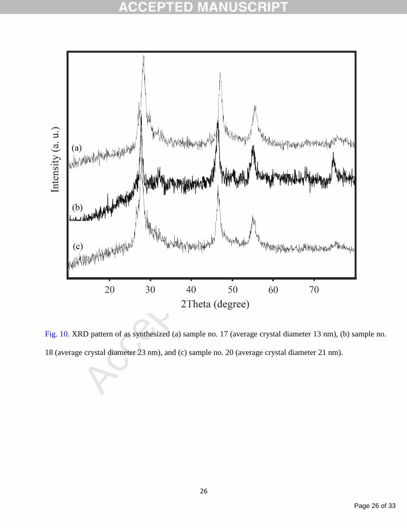
sample phase and size distribution. XRD pattern of the samples obtained by CuSO4 as cupper precursor
(Fig. 10) confirmed that these samples are in the same crystalline phase with those which obtained by
bis(2-hydoxyacetophenato)copper(II) but by variation in sulfide precursors the crystallinity of samples and
average crystal diameter changed and the smallest crystal diameter was observed for those obtained by
TAA as sulfide precursor.
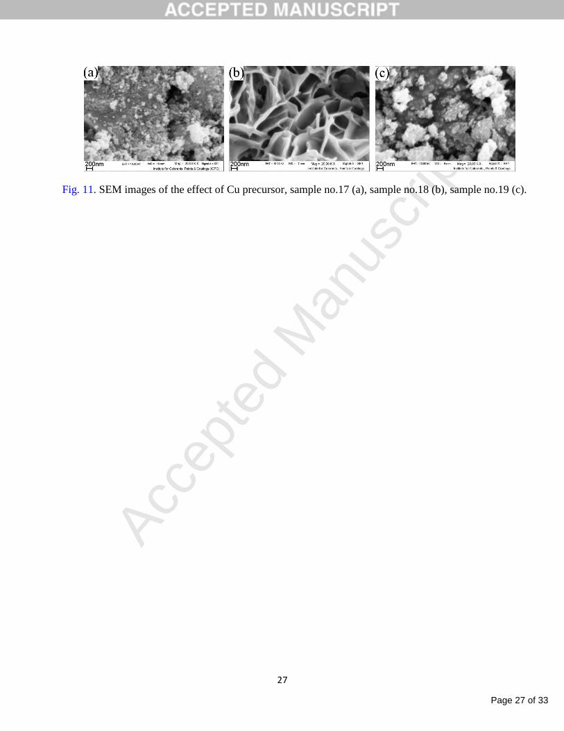
To investigate copper precursor effect on reaction and sample morphology, some experiments have been
repeated with CuSO4. Fig. 11 shows the SEM images of the samples 17-19 obtained by reaction between
CuSO4 and different sulfur source. Similarly with those experiments which have been done by [bis(2-
hydoxyacetophenato)copper(II)], the CuInS2 nanostructures synthesized using different sulfide source
differ in the structure and morphology In the case of TAA and TU nanoparticles obtained which differ in
size (Fig. 11a, c respectively) and when thiosemicarbazid was used, flower shaped structure observed
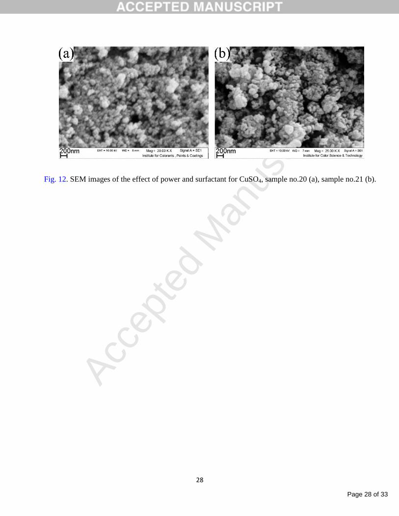
(Fig. 11b). Fig. 12 shows the SEM images of the samples 20 and 21 related to the effect of surfactant.
When TU was used at 65 W (sample no. 20, Fig. 12a) the samples were homogenous and narrow
distribution was seen while those obtained at 80 W were fused to each other (sample no. 19, Fig. 11c).
Fig. 12b shows the SEM images of the samples 21 that obtained with no surfactant. It is clear that larger
and non-uniform particles obtained in comparison with sample 20 which obtained by the use of surfactant.
In general, From comparison between results of experiments prepared by [bis(2-
Page 10 of 33
Accep
ted
Man
uscr
ipt
10
hydoxyacetophenato)copper(II)] and CuSO4 it can be concluded that; when CuSO4 is used, surfactant plays
a significant role in controlling the size and morphology of CuInS2 nanostructure while in the case of
[bis(2-hydoxyacetophenato)copper(II)] SDS has not important role on size but can improve size
distribution of product. In the most cases, the surface passivation reagents, including surfactant molecules,
are needed to prevent the nanoparticles from aggregation [39].
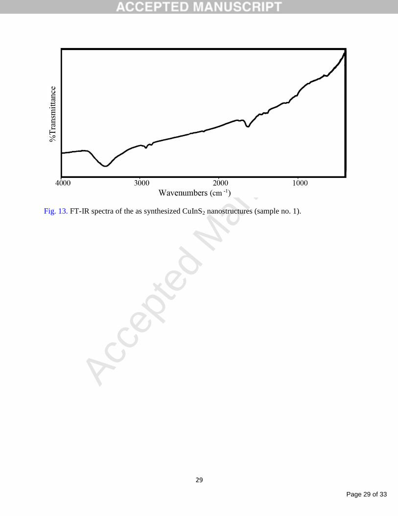
To investigate that the surface of particle is capped with organic material or not Fourier transformed
infrared (FT-IR) of the as-synthesized samples was performed (Fig. 13). It is obvious that there is no
significant impurity but there may be less organic impurity capped nanoparticles which may arise from
[bis(2-hydoxyacetophenato)copper(II)] as a weak peak at 1629 cm-1
that can be corresponded to C=O
symmetry stretching vibration. A weak peak at 3442 cm-1
can be attributed to stretching vibration of the
O-H band that is absorbed on the surface of the particle [7].
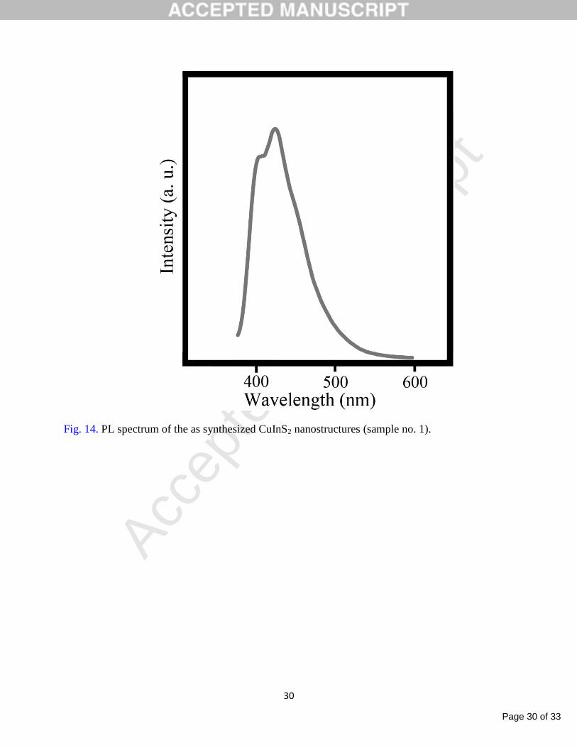
The size of the semiconductor nanocrystals can directly determine their optical properties. Optical
properties of samples were investigated using a Perkin-Elmer LS-55 luminescence spectrometer with an
excitation slit width of 5 nm and an emission slit width of 5 nm. A sharp and strong peak centered at a
wavelength of 421 nm (excitation at 352 nm) is observed (Fig. 14). As compared to the band gap of bulk
CuInS2 which is 1.54 eV [4–6] the absorption spectrum of as-prepared samples exhibits a blue-shift (2.94
eV, 421 nm).
However, as presented above, by an ultrasonic route, CuInS2 nanostructures were synthesized with use
of different precursors. In comparison with other chemical methods which have been used for preparation
of CuInS2 nanocrystals [10–20] current method is very fast and also using ultrasound radiation will lead to
high yields and smaller particles [40].
4. Conclusions:
Page 11 of 33
Accep
ted
Man
uscr
ipt
11
In summary, we reported a chemical method for preparation and controlling the morphologies of
nanosized CuInS2. CuInS2 nanostructures were successfully prepared via ultrasonic-assisted method. This
method is simple and can be easily controlled. In this work different sulfur sources were used, also effects
of different parameters including ultrasonic power, time, surfactant and copper source were investigated.
The morphology, structure and composition of the yielded nanostructures were confirmed by XRD, EDX,
SEM, FT-IR and PL. It was found that the product was pure CuInS2 which obtained after annealing at 350
°C. Optical studies confirmed quantum confinement effects for nanoparticles. It was revealed that when
[bis(2-hydoxyacetophenato)copper(II)] was used SDS did not show significant effect on size but in the
case of CuSO4 it regulates sample size and is necessary for preparation of nanosized CuInS2.
Acknowledgement:
Authors are grateful to the council of Iran National Science Foundation and University of Kashan for
supporting this work by Grant No (159271/20).
Page 12 of 33
Accep
ted
Man
uscr
ipt
12
References:
[1] J.Á. García, Characterisation of CuInS2 films for solar cell applications by Raman Spectroscopy,
Barcelona. (2002) pp. 12.
[2] K. Muller, R. Scheer, Y. Burkov , D. Schmeißer, J. Thin. Solid. Films. 451–452 (2004) 120–123.
[3] R. Klenk, R. Könenkamp, T. Matthes, R. Scheer, S. Siebentritt, and A. Weidinger, J. Thin Solid.
Films. 361-362 (2000) 533–539.
[4] T. T. John, M. Mathew, C. SudhaKartha, K.P.Vijayakumar, T.Abe, Y. Kashiwaba, Sol. Energy. Mater.
sol. Cells. 89 (2005) 27–36
[5] Bera, S. IlSeok, J. Solid. State. Chem. 183 (2010) 1872–1877.
[6] A. Antony, A. S. Asha, R. Yoosuf, R. Manoj, M. K. Jayaraj, Sol. Energy. Mater. sol. Cells. 81 (2004)
407–417.
[7] S. Peng, F. Cheng, J. Liang, Z. Tao, J. Chen, J. Alloys Compd. 481 (2009) 786–791.
[8] X. H. Xu, F. Wanga, J. J. Liu, K. C. Park, M. Fujishige, Sol. Energy. Mater. sol. Cells. 95 (2011) 791–
79.
[9] J.J. Nairn, P.J. Shapiro, B. Twamley, T. Pounds, R. von Wandruszka, T.R. Fletcher, Nano. Lett., 6
(2006) 1218–1223.
[10] Y. Jiang, Y. Wu, X. Mo, W.C. Yu, Y. Xie and Y. T. Qian, Inorg. Chem. 39 (2000) 2964–2965.
[11] J.P. Xiao, Y. Xie, R. Tang, Y.T. Qian, J. Solid. State . Chem. 161 (2001) 179–183.
[12] K. Wakita, M. Iwai, Y. Miyoshi, H. Fujibuchi, A. Ashida, Compos. Sci. Technol. 65 (2005) 765–767.
Page 13 of 33
Accep
ted
Man
uscr
ipt
13
[13] W.M. Du, X.F. Qian, J. Yin, Q. Gong, Chem. Eur J. 13 (2007) 8840–8846.
[14] S.J. Peng, J. Liang, L. Zhang, Y.H. Shi and J. Chen, J. Cryst Growth, 305 (2007) 99–103.
[15] H.M. Hu, B.J. Yang, X.Y. Liu, R. Zhang and Y.T. Qian, Inorg. Chem. Commun, 7 (2004) 563–565.
[16] S.Han, M. Kong, Y. Guo, M. Wang, J. Mater. Lett. 63 (2009) 1192–1194
[17] N. Solanki, R. Sengupta, Z.V.P. Murthy, solid. state sience. 12 (2010) 1560–1566.
[18] J.S. Gardner, E. Shurdha, C.M. Wang, L.D. Lau, R.G. Rodriguez and J.J. Pak, J. Nanopart Res. 10
(2008) 633–641.
[19] A.Y. Zhang, Q. Ma, M.K. Lu, G.W. Yu, Y.Y. Zhou, Z.F. Qiu, Cryst Growth Des, 8 (2008) 2402–
2405.
[20] G.Z. Shen, D. Chen, K.B. Tang, Z. Fang, J. Sheng and Y.T. Qian, J. Cryst Growth. 254 (2003) 75–
79.
[21] R. Nomura, Y. Sekl, H. Matsuda, J. Mater. Chem. 2 (1992) 765–766.
[22] Y. Yamamoto, T. Yamaguchi, Y. Denizu, T. Tanaka, A. Yoshida, Thin Solid Films 281 (1996) 372–
374.
[23] Y.D. Tembhurkar, Mater. Sci. 20 (1997) 1011–1014.
[24] H. Metzner, T. Hahn, J.H. Bremar, J. Conrad, Appl. Phys. Lett. 69 (1996) 1900–1902.
[25] K. Djessas, G. Masse , M. Ibannaim, J. Electrochem. Soc. 147 (2000) 1235–1239.
[26] S.L. Castro, S.G. Bailey, R.P. Raffaelle, K.K. Banger, A.F. Hepp, Chem. Mater. 15 (2003) 3142–
3147.
Page 14 of 33
Accep
ted
Man
uscr
ipt
14
[27] T. Nyari, P. Barvinschi, R. Ba ies, P. Vla zan, F. Barvinschi, I.Dekany, J. Crystal Growth. 275 (2005)
2383–2387.
[28] D. P. Dutta , G. Sharma , Mater. Lett. 60 (2006) 2395–2398.
[29] B. Chen, H. Zhong, W. Zhang, Z.Tan, Y. Li, C. Yu, T. Zhai, Y. Bando, S. Yang, B. Zou, Adv Func.
Mater. 22 (2012) 2081–2088.
[30] H. Wang, Z. Shao, B. Chen, T. Zhang, F. Wang, H. Zhong, RSC Adv. 2 (2012) 2675–2677.
[31] H. Zhong, S. S. Lo, T. Mirkovic, Y. Li, Y. Ding, Y. Li, G. D. Scholes, ACS Nano. 4 (2010) 5253–
5262.
[32] K. S. Suslick, M. M. Fang, T. Hyeon, J. Am. Chem. Soc. 118 (1996) 11960–11961.
[33] C. Deng, H. Hu, X. Ge, C. Han, D. Zhao, G. Shao, Ultrason. Sonochem. 18 (2011) 932–937.
[34] K. Prasad, D. V. Pinjari, A. B. Pandit, S. T. Mhaske, Ultra. Sonochem. 17 (2010) 409–415.
[35] M. Salavati-Niasari, M. Shaterian, M.R. Ganjali, P. Norouzi, J. Mol. Catal. A: Chem. 261 (2007)
147–155.
[36] L. Andronic, L. Isac, A. Duta, J. Photoch. Photobio. A. 221 (2011) 30–37.
[37] V. Swayambunathan, D. Hayes, K. Schmidt, Y. Liao, D. Meisel, J. Am. Chem. Soc. 112 (1990)
3831–3837.
[38] R. Cayzac, F. Boulc’h, M. Bendahan, P. Lauque, P. Knauth, Mater. Sci. Engin B 157 (2009) 66–71.
[39] M. Shang, W. Wang, L. Zhou, S. Sun, W. Yin, J. Hazard. Mater. 172 (2009) 338–344.
[40] A. Gedanken, Ultrason. Sonochem. 11 (2004) 47–55.
Page 15 of 33
Accep
ted
Man
uscr
ipt
15
Figure caption
Fig. 1. XRD pattern of as synthesized sample (a) not annealed, (b) annealed at 350oC for 1h (c) annealed
at 350oC for 1h under Argon atmosphere.
Fig. 2. XRD pattern of as synthesized (a) sample no. 2 (average crystal diameter 25 nm), (b) sample no. 3
(average crystal diameter 27 nm), (c) sample no. 4 (average crystal diameter 35 nm), (d) sample no. 5
(average crystal diameter 20 nm), and (e) sample no. 6 (average crystal diameter 30 nm).
Fig. 3. EDX spectrum of the as synthesized CuInS2 nanostructures (sample no. 1).
Fig. 4. XPS spectra of as-synthesized product (sample no. 1): (a) survey spectrum; (b) Cu2p; (c) In3d; and
(d) S2p.
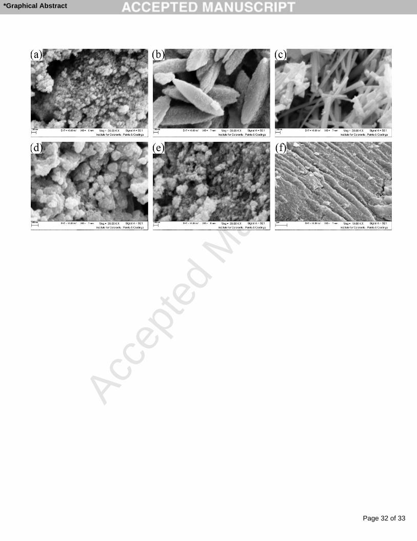
Fig. 5. SEM images of samples obtained with different sulfide source, sample no.1 (a), sample no.2 (b),
sample no.3 (c), sample no.4 (d), sample no.5 (e), and sample no.6 (f).
Fig. 6. SEM images of samples obtained at different times, sample no.7 (a), sample no.8 (b), sample no.9
(c).
Fig. 7 SEM images of samples obtained at different powers, sample no.10 (a), sample no.11 (b), sample
no.12 (c).
Fig. 8. XRD pattern of sample no. 15.
Fig. 9. SEM images of surfactant and ultrasonic effect, sample no.13 (a), sample no.14 (b), sample no.15
(c), sample no.16 (d) which obtained without annealing.
Fig. 10. XRD pattern of as synthesized (a) sample no. 17 (average crystal diameter 13 nm), (b) sample no.
18 (average crystal diameter 23 nm), and (c) sample no. 20 (average crystal diameter 21 nm).
Fig. 11. SEM images of the effect of Cu precursor, sample no.17 (a), sample no.18 (b), sample no.19 (c).
Fig. 12. SEM images of power and surfactant effect for CuSO4, sample no.20 (a), sample no.21 (b).
Page 16 of 33
Accep
ted
Man
uscr
ipt
16
Fig. 13. FT-IR spectra of the as synthesized CuInS2 nanostructures (sample no. 1).
Fig. 14. PL spectrum of the as synthesized CuInS2 nanostructures (sample no. 1).
Table 1. Reaction conditions for preparation of CuIS2 nanopstructure.
Page 17 of 33
Accep
ted
Man
uscr
ipt
17
Fig. 1.
XRD pattern of as synthesized sample (a) not annealed, (b) annealed at 350 oC for 1 h (c) annealed at 350
oC for 1 h under Argon atmosphere.
Page 18 of 33
Accep
ted
Man
uscr
ipt
18
Fig. 2. XRD pattern of as synthesized (a) sample no. 2 (average crystal diameter 25 nm), (b) sample no. 3
(average crystal diameter 27 nm), (c) sample no. 4 (average crystal diameter 35 nm), (d) sample no. 5
(average crystal diameter 20 nm), and (e) sample no. 6 (average crystal diameter 30 nm).
Page 19 of 33
Accep
ted
Man
uscr
ipt
19
Fig. 3. EDX spectrum of the as synthesized CuInS2 nanostructures (sample no. 1).
Page 20 of 33
Accep
ted
Man
uscr
ipt
20
Fig. 4. XPS spectra of as-synthesized product (sample no. 1): (a) survey spectrum; (b) Cu2p; (c) In3d; and
(d) S2p.
Page 21 of 33
Accep
ted
Man
uscr
ipt
21
Fig. 5. SEM images of samples obtained with different sulfide source, sample no.1 (a), sample no.2 (b),
sample no.3 (c), sample no.4 (d), sample no.5 (e), and sample no.6 (f).
Page 22 of 33
Accep
ted
Man
uscr
ipt
22
Fig. 6. SEM images of samples obtained at different times, sample no.7 (a), sample no.8 (b), sample no.9
(c).
Page 23 of 33
Accep
ted
Man
uscr
ipt
23
Fig. 7. SEM images of samples obtained at different powers, sample no.10 (a), sample no.11 (b), sample
no.12 (c).
Page 24 of 33
Accep
ted
Man
uscr
ipt
24
Fig. 8. XRD pattern of sample no. 15.
Page 25 of 33
Accep
ted
Man
uscr
ipt
25
Fig. 9. SEM images of surfactant and ultrasonic effect, sample no.13 (a), sample no.14 (b), sample no.15
(c), sample no.16 (d) which obtained without annealing.
Page 26 of 33
Accep
ted
Man
uscr
ipt
26
Fig. 10. XRD pattern of as synthesized (a) sample no. 17 (average crystal diameter 13 nm), (b) sample no.
18 (average crystal diameter 23 nm), and (c) sample no. 20 (average crystal diameter 21 nm).
Page 27 of 33
Accep
ted
Man
uscr
ipt
27
Fig. 11. SEM images of the effect of Cu precursor, sample no.17 (a), sample no.18 (b), sample no.19 (c).
Page 28 of 33
Accep
ted
Man
uscr
ipt
28
Fig. 12. SEM images of the effect of power and surfactant for CuSO4, sample no.20 (a), sample no.21 (b).
Page 29 of 33
Accep
ted
Man
uscr
ipt
29
Fig. 13. FT-IR spectra of the as synthesized CuInS2 nanostructures (sample no. 1).
Page 30 of 33
Accep
ted
Man
uscr
ipt
30
Fig. 14. PL spectrum of the as synthesized CuInS2 nanostructures (sample no. 1).
Page 31 of 33
Accep
ted
Man
uscr
ipt
31
Table1. Reaction conditions for preparation of CuIS2 nanopstructure.
Sample
No. Copper source Sulfur source
Power
(W)
Time
(Min) Surfactant
Temperature of
annealing
1 bis(2-hydoxyacetophenato)copper(II) Thioacetamide (TAA) 80 35 SDS 350
2 bis(2-hydoxyacetophenato)copper(II) Sodium Thiosulfate 80 35 SDS 350
3 bis(2-hydoxyacetophenato)copper(II) Thioglycolic acid (TGA) 80 35 SDS 350
4 bis(2-hydoxyacetophenato)copper(II) Thiourea (TU) 80 35 SDS 350
5 bis(2-hydoxyacetophenato)copper(II) Thiosemicarbazid 80 35 SDS 350
6 bis(2-hydoxyacetophenato)copper(II) L-cysteine 80 35 SDS 350
7 bis(2-hydoxyacetophenato)copper(II) Thioacetamide (TAA) 80 20 SDS 350
8 bis(2-hydoxyacetophenato)copper(II) Thioacetamide (TAA) 80 50 SDS 350
9 bis(2-hydoxyacetophenato)copper(II) Thioacetamide (TAA) 80 65 SDS 350
10 bis(2-hydoxyacetophenato)copper(II) Thioacetamide (TAA) 45 35 SDS 350
11 bis(2-hydoxyacetophenato)copper(II) Thioacetamide (TAA) 55 35 SDS 350
12 bis(2-hydoxyacetophenato)copper(II) Thioacetamide (TAA) 65 35 SDS 350
13 bis(2-hydoxyacetophenato)copper(II) Thioacetamide (TAA) 65 35 — 350
14 bis(2-hydoxyacetophenato)copper(II) Thioacetamide (TAA) — — SDS 350
15 bis(2-hydoxyacetophenato)copper(II) Thioacetamide (TAA) — — — 350
16 bis(2-hydoxyacetophenato)copper(II) Thioacetamide (TAA) — — SDS —
17 CuSO4 Thioacetamide (TAA) 80 35 SDS 350
18 CuSO4 Thiosemicarbazid 80 35 SDS 350
19 CuSO4 Thiourea (TU) 80 35 SDS 350
20 CuSO4 Thiourea (TU) 65 35 SDS 350
21 CuSO4 Thiourea (TU) 65 35 — 350
Page 32 of 33
Accep
ted
Man
uscr
ipt
*Graphical Abstract
Page 33 of 33
Accep
ted
Man
uscr
ipt
Research highlights
CuInS2 nanoparticles were synthesized by ultrasonic assisted method.
CuInS2 nanoparticles obtained after annealing at 350 °C for 1h.
The effect of some parameters including ultrasonic was investigated.
*Highlights
Related Documents


![Relating aerosol mass spectra to composition and nanostructure of soot particleslup.lub.lu.se/.../54154413/Malmborg_et_al._2019_Carbon.pdf · carbon nanostructure [13,14], hydrogen](https://static.cupdf.com/doc/110x72/6110bc7c7b716b3cf61b4566/relating-aerosol-mass-spectra-to-composition-and-nanostructure-of-soot-carbon-nanostructure.jpg)