Synopsys Confidential Information © 2021 Synopsys, Inc. All rights reserved. Inferring Microchip PolarFire RAM Blocks Synopsys® Application Note, April 2021 Microchip PolarFire devices support the RAM1K20 and RAM64X12 RAM macros. This application note provides a general description of the Microchip PolarFire RAM block components and describes how to infer it with the Synplify® Pro synthesis tool. See the following topics for details: • PolarFire RAM Blocks, on page 2 • Inferring PolarFire RAM Blocks, on page 3 • Controlling Inference With syn_ramstyle Attribute, on page 4 • Read/Write Address Collision Check, on page 6 • RAM Inference in Low Power Mode Using BLK Pins, on page 7 • Write Byte-Enable Support for RAM, on page 7 • RAM Inference for ROM Support, on page 7 • RAM Initialization Support, on page 8 • RAMINDEX Property Switch, on page 8 • Coding Style Examples, on page 8 • Inferring RAM Blocks for Seqshift, on page 131 • Current Limitations, on page 145

Welcome message from author
This document is posted to help you gain knowledge. Please leave a comment to let me know what you think about it! Share it to your friends and learn new things together.
Transcript

Inferring Microchip PolarFire RAM BlocksSynopsys® Application Note, April 2021
Microchip PolarFire devices support the RAM1K20 and RAM64X12 RAM macros. This application note provides a general description of the Microchip PolarFire RAM block components and describes how to infer it with the Synplify® Pro synthesis tool.
See the following topics for details:
• PolarFire RAM Blocks, on page 2
• Inferring PolarFire RAM Blocks, on page 3
• Controlling Inference With syn_ramstyle Attribute, on page 4
• Read/Write Address Collision Check, on page 6
• RAM Inference in Low Power Mode Using BLK Pins, on page 7
• Write Byte-Enable Support for RAM, on page 7
• RAM Inference for ROM Support, on page 7
• RAM Initialization Support, on page 8
• RAMINDEX Property Switch, on page 8
• Coding Style Examples, on page 8
• Inferring RAM Blocks for Seqshift, on page 131
• Current Limitations, on page 145
Synopsys Confidential Information © 2021 Synopsys, Inc. All rights reserved.
2 Inferring Microchip PolarFire RAM Blocks
PolarFire RAM BlocksPolarFire devices support two types of RAM macros:
• RAM1K20, on page 2
• RAM64X12, on page 2
RAM1K20RAM1K20 (LSRAM) memory block has the following features:
• 16,896 memory bits with ECC and 20,480 memory bits without ECC.
• Two independent data ports, A and B.
• Infers single-port, simple dual-port, and true dual-port RAMs.
• For two-port mode (simple dual-port), port A is the read-port and port B is the write-port.
• Optional pipeline register with a separate enable and synchronous reset at the read-data port.
• Synchronous read and write operations.
• Independent clock for each port. The memory is triggered at the rising edge of the clock.
• Does not allow read and write operations on the same location at the same time. It has no detection and collision prevention.
• Feed-through write mode available to enable immediate access to the write data and read-before-write option in dual-port mode.
• Read-enable control for dual-port and two-port modes.
• Allows read from both ports at the same location.
• Raises flags to indicate single-bit-correct and double-bit-detect when ECC is enabled.
RAM64X12RAM64X12 (URAM) memory block has the following features:
• URAM block contains 768 memory bits and is a two-port memory providing one write port and one read port.
• Write operations are always synchronous.
• Read-address can be synchronous or asynchronous.
• Read-data ports have output registers for pipeline mode operation.
• Does not allow read and write on the same location at the same time. It has no collision prevention or detection.
Synopsys Confidential Information © 2021 Synopsys, Inc. All rights reserved.
3 Inferring Microchip PolarFire RAM Blocks
Inferring PolarFire RAM BlocksThe synthesis tool identifies the RAM structure from the RTL and implements LSRAM or URAM block.
The RAM block is selected for mapping using the following criteria:
• For true dual-port synchronous read memory, the synthesis tool maps the LSRAM block regardless of its memory size.
• For simple dual-port RAM symmetric synchronous URAM memory:
– If both read address and read data registers are bypassed.
– If RAM depth <= 64 and width <= 324 or if RAM depth <= 128 and width <= 12, the tool infers RAM64x12, otherwise the tool maps to LSRAM.
– If the size of memory is less than or equal to 12 bits, the software maps to registers.
• For simple dual-port, single-port, or asynchronous read memory, if the size of the memory is 12 bits or more, the software maps to URAM. If the size of the memory is less than 12 bits, the synthesis tool maps to registers.
Note: You can override this default behavior using the syn_ramstyle attribute. See Controlling Inference With syn_ramstyle Attribute, on page 4.
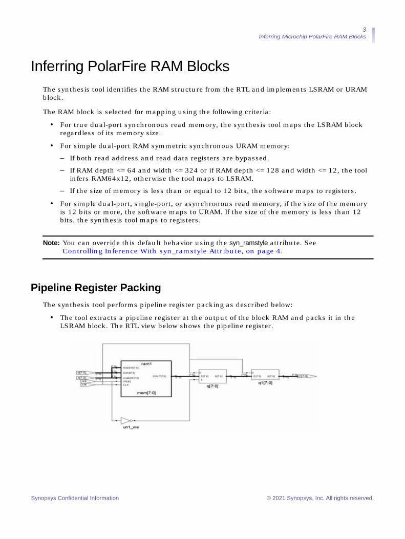
Pipeline Register PackingThe synthesis tool performs pipeline register packing as described below:
• The tool extracts a pipeline register at the output of the block RAM and packs it in the LSRAM block. The RTL view below shows the pipeline register.
Synopsys Confidential Information © 2021 Synopsys, Inc. All rights reserved.
4 Inferring Microchip PolarFire RAM Blocks
• The pipeline register q1 [7:0] is not packed when the register q [7:0] has asynchronous or synchronous reset.
• The pipeline register q1 [7:0] can have asynchronous reset or synchronous reset or clock enable.
Controlling Inference With syn_ramstyle AttributeUse the syn_ramstyle attribute to manually control how the PolarFire RAM blocks are inferred, as described below. To map to:
• RAM1K20—use syn_ramstyle = "lsram"
• RAM64x12—use syn_ramstyle = "uram"
• registers—use syn_ramstyle = "registers"
You can apply the attribute globally, or to a RAM instance or module.
Constraint File Syntax and Exampledefine_attribute {signalName[bitRange]} syn_ramstyle {string} define_global_attribute syn_ramstyle {string}
When editing a constraint file to apply the syn_ramstyle attribute, ensure to include the range of the signal with the signal name. For example:
define_attribute {mem1[7:0]} syn_ramstyle {registers}; define_attribute {mem2[7:0]} syn_ramstyle {lsram}; define_attribute {mem3[7:0]} syn_ramstyle {uram};
Verilog Syntax and Exampleobject /* synthesis syn_ramstyle = "string" */;
where object is a register definition signal. The data type is string. Here is an example:
module ram4 (datain,dataout,clk); output [31:0] dataout; input clk; input [31:0] datain; reg [7:0] dataout[31:0] /* synthesis syn_ramstyle="uram" */; // Other code
Synopsys Confidential Information © 2021 Synopsys, Inc. All rights reserved.

5 Inferring Microchip PolarFire RAM Blocks
VHDL Syntax and Exampleattribute syn_ramstyle of object : objectType is "string" ;
where object is a signal that defines a RAM or a label for a component instance. The data type is string.
library ieee; use ieee.std_logic_1164.all; library synplify;entity ram4 is port (d : in std_logic_vector(7 downto 0);addr : in std_logic_vector(2 downto 0); we : in std_logic; clk : in std_logic;ram_out : out std_logic_vector(7 downto 0) ); end ram4;architecture rtl of ram4 is type mem_type is array (127 downto 0) of std_logic_vector (7 downto 0); signal mem : mem_type; -- mem is the signal that defines the RAMattribute syn_ramstyle : string; attribute syn_ramstyle of mem : signal is "lsram"; -- Other code
Note the following:
• If your RTL code includes a true dual-port synchronous read memory, then you cannot use syn_ramstyle = "uram" to infer RAM64X12, since true dual-port mode is not supported. The synthesis software ignores this attribute and infers RAM1K20.
• If your RTL code includes asynchronous memory, then you cannot use syn_ramstyle = "lsram" to infer RAM1K20, since asynchronous memory is not supported. The synthesis software ignores this attribute and infers RAM64X12.
• When you do not want to use RAM resources, apply the value of registers to the syn_ramstyle attribute on the RAM instance name or signal driven by the RAM.
• The syn_ramstyle attribute supports the values of no_rw_check and rw_check. By default, the synthesis tool does not generate glue logic for read or write address collision. Use syn_ramstyle="rw_check" to insert glue logic for read write address collision. Use syn_ram-style="no_rw_check" to prevent glue logic insertion. See Read/Write Address Collision Check, on page 6
Synopsys Confidential Information © 2021 Synopsys, Inc. All rights reserved.

6 Inferring Microchip PolarFire RAM Blocks
Read/Write Address Collision CheckThe synthesis software does not perform read or write address collision check when RAM is inferred. The tool does not insert glue logic around RAM to prevent the read or write address collision during write operation.
If read and write to the same address occurs simultaneously in your design, use syn_ramstyle="rw_check" or enable the Read Write Check on RAM option on the Implementation Options Device panel, to perform read or write address collision check. The tool then inserts glue logic around the RAM to prevent read or write address collision during the write operation, while retaining the RTL behavior.
The different modes include:
• Write-first mode—write operations precede read when a collision occurs. Data is first written into memory and then the same data is read.
• Read-first mode—read operations precede write when a collision occurs. Old data is read first and then new data is written into memory.
• No change mode—output of the RAM does not change when a collision occurs.
Note the following, if the Read Write Check on RAM option is enabled:
• The PolarFire LSRAM architecture supports read-before-write mode (previous content of the memory appears on the corresponding read-data port before it is overwritten. This setting is invalid when the width of at least one port is 20 and the two-port mode is in effect), write-first mode (active feed-through mode) and no change mode (disabled feed-through mode), when used as a single-port RAM.
• When a single-port RAM with write -first mode is mapped to LSRAM, no glue logic is created around the RAM.
• When RAM written in read-first mode is mapped to LSRAM, no glue logic is created.
• For no change mode, no glue logic is created because the RAM output does not change when a collision occurs.
• For simple dual-port and true dual-port RAM in write-first mode, glue logic is created. Glue logic is also created for single-port RAM when it is mapped to URAM.
• If read/write check creates glue logic, then the pipeline register cannot be packed into the block RAM.
Synopsys Confidential Information © 2021 Synopsys, Inc. All rights reserved.
7 Inferring Microchip PolarFire RAM Blocks
RAM Inference in Low Power Mode Using BLK PinsBy default, the tool fractures wide RAMs by splitting the data width to improve timing.
The tool uses the BLK pins of the RAM for reducing power consumption by fracturing wide RAMs on the address width.
To enable this feature, set global option low_power_ram_decomp 1 in the project file (*.prj). The tool uses this option to fracture wide RAMs on the address width to infer RAM in low power mode. The tool uses the BLK pin to select a RAM for a particular address and OR gates at the output to select the output from RAM blocks.
The control of individual RAM inference to turn on or turn off low power mode is supported through the synthesis attribute syn_ramstyle.
Add syn_ramstyle = "low_power" to turn on low power inference if the global option is off. Add syn_ramstyle = "no_low_power" to turn off low power inference if the global option is on.
Write Byte-Enable Support for RAMIn case of a RAM with n write-enables to control the writing of data into memory locations, the Synplify Pro compiler creates n sub-instances of the RAM with different write-enables. The Synplify Pro mapper merges these multiple RAM blocks into a single or multiple Block RAMs based on the threshold and the number of write-enables. The write byte-enable (A_WEN/B_WEN [1:0]) pin of Block RAM primitives are configured to control the write operation in Block RAMs.
RAM Inference for ROM SupportBy default, ROM is implemented using RAM1K20 and RAM64x12 depending on the RAM threshold values. An asynchronous-ROM is always mapped to RAM64x12.
This feature is supported for RAMs inferred in a non-low power (speed) mode.
Note: Synplify Pro maps the ROM constructs to RAM only if the option -rom_map_logic in the synthesis *.prj file is set to value 0. For example, set_option -rom_map_logic 0.
Synopsys Confidential Information © 2021 Synopsys, Inc. All rights reserved.

8 Inferring Microchip PolarFire RAM Blocks
RAM Initialization SupportINIT value is supported for the RAM1K20 and RAM64x12 RAM blocks in the PolarFire device.
RAMINDEX Property SwitchTo disable generation of the RAMINDEX property in RAM1K18_RT and RAM64X18_RT RAM blocks, add the disable_ramindex switch to the project file (prj):
Usage (disable RAMINDEX): set_option -disable_ramindex 1
Coding Style Examples• Inferring RAM1K20 and RAM64X12 RAM Blocks, on page 8
• Inferring RAM Blocks for ROM, on page 106
• Inferring RAM Blocks for Write Byte-enable RAM, on page 117
• Inferring Initialized RAM blocks, on page 128
Inferring RAM1K20 and RAM64X12 RAM BlocksThe following examples show how to infer RAM1K20 and RAM64X12 RAM blocks:
• Example 1: Single-port RAM - LSRAM (write-first mode), on page 11
• Example 2: Single-port RAM - URAM (write-first mode), on page 12
• Example 3: Single-port RAM with Pipeline Register - LSRAM (write-first mode), on page 13
• Example 4: Single-port RAM with Pipeline Register - URAM (write-first mode), on page 14
• Example 5: Simple Dual-port RAM - LSRAM (write-first mode), on page 15
• Example 6: Simple Dual-port RAM - URAM (write-first mode), on page 16
• Example 7: Simple Dual-port RAM with Pipeline Register - LSRAM (write-first mode), on page 17
• Example 8: Simple Dual-port RAM with Pipeline Register - URAM (write-first mode), on page 18
• Example 9: True Dual-port RAM (single clock), on page 19
Synopsys Confidential Information © 2021 Synopsys, Inc. All rights reserved.
9 Inferring Microchip PolarFire RAM Blocks
• Example 10: True Dual-port RAM (multiple clocks), on page 21
• Example 11: True Dual-port RAM with Pipeline Register, on page 22
• Example 12: Single-port RAM (asynchronous read) URAM (read-first mode), on page 24
• Example 13: Simple Dual-port RAM (asynchronous read) URAM (read- first mode), on page 25
• Example 14: Single-port RAM (asynchronous read) with Pipeline Register URAM (read-first mode), on page 26
• Example 15: Simple Dual-port RAM (asynchronous read) and Pipeline Register with Clock Enable URAM (no change mode), on page 27
• Example 16: Single-port RAM LSRAM (no change mode), on page 30
• Example 17: Single-port RAM with One Pipelined Register on the Read Port (sync-sync) (no change mode), on page 32
• Example 18: Single-port RAM with One Pipelined Register on the Read Port (sync-sync), on page 33
• Example 19: Single-port RAM with One Pipelined Register on the Read Port (sync-sync), on page 34
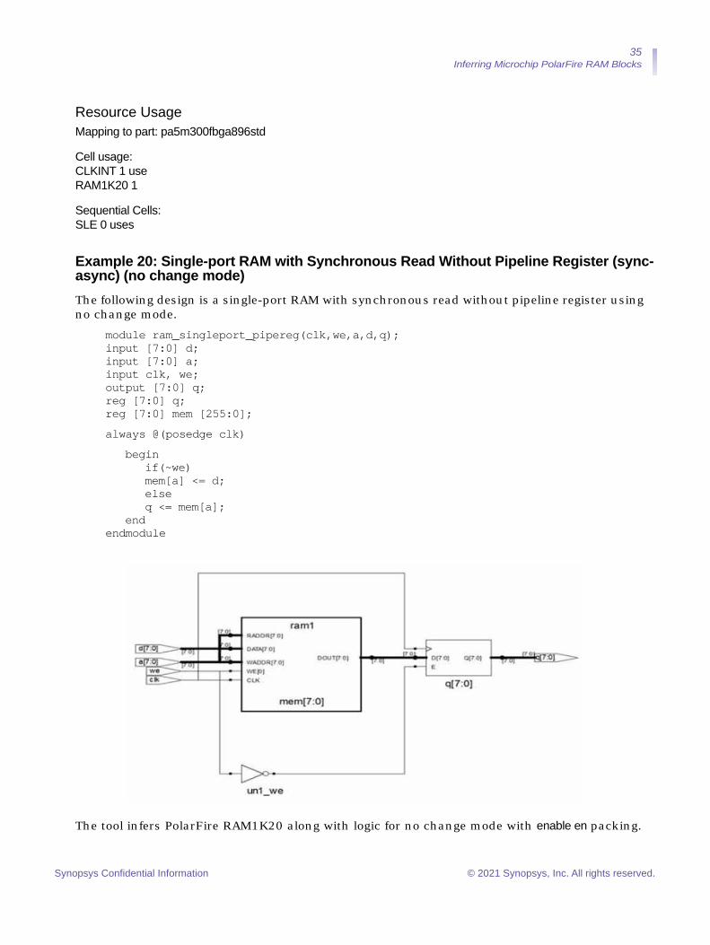
• Example 20: Single-port RAM with Synchronous Read Without Pipeline Register (sync-async) (no change mode), on page 35
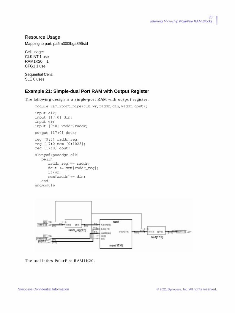
• Example 21: Simple-dual Port RAM with Output Register, on page 36
• Example 22: Single-port RAM with Output Registers (VHDL), on page 37
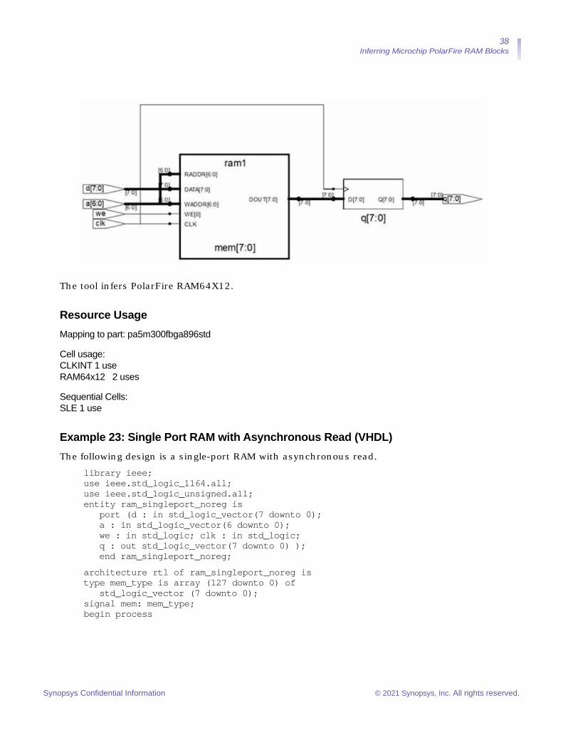
• Example 23: Single Port RAM with Asynchronous Read (VHDL), on page 38
• Example 24: Simple Dual-port RAM with Output Register and Read Address Register (VHDL), on page 40
• Example 25: True Dual-port RAM with Read Address Register (VHDL), on page 41
• Example 26: Simple Dual-port (two-port) RAM with Read Address Register (512 x 40 configurations), on page 42
• Example 27: True Dual-port RAM with Output Registered, Pipelined, and Non-pipelined Version (VHDL), on page 43
• Example 28: Simple Dual-port (two-port) RAM with Asynchronous Reset for Pipeline Register, on page 48
• Example 29: Single-port RAM with Synchronous Reset for Pipeline Register (LSRAM), on page 50
• Example 30: True Dual-port RAM with Asynchronous Reset for Pipeline Register (LSRAM), on page 51
• Example 31: Single-port RAM with Synchronous Reset for Pipeline Register (URAM) (syn_ramstyle=rw_check), on page 52
Synopsys Confidential Information © 2021 Synopsys, Inc. All rights reserved.

10 Inferring Microchip PolarFire RAM Blocks
• Example 32: Simple dual-port RAM with Output Register using syn_ram-style=rw_check, on page 54
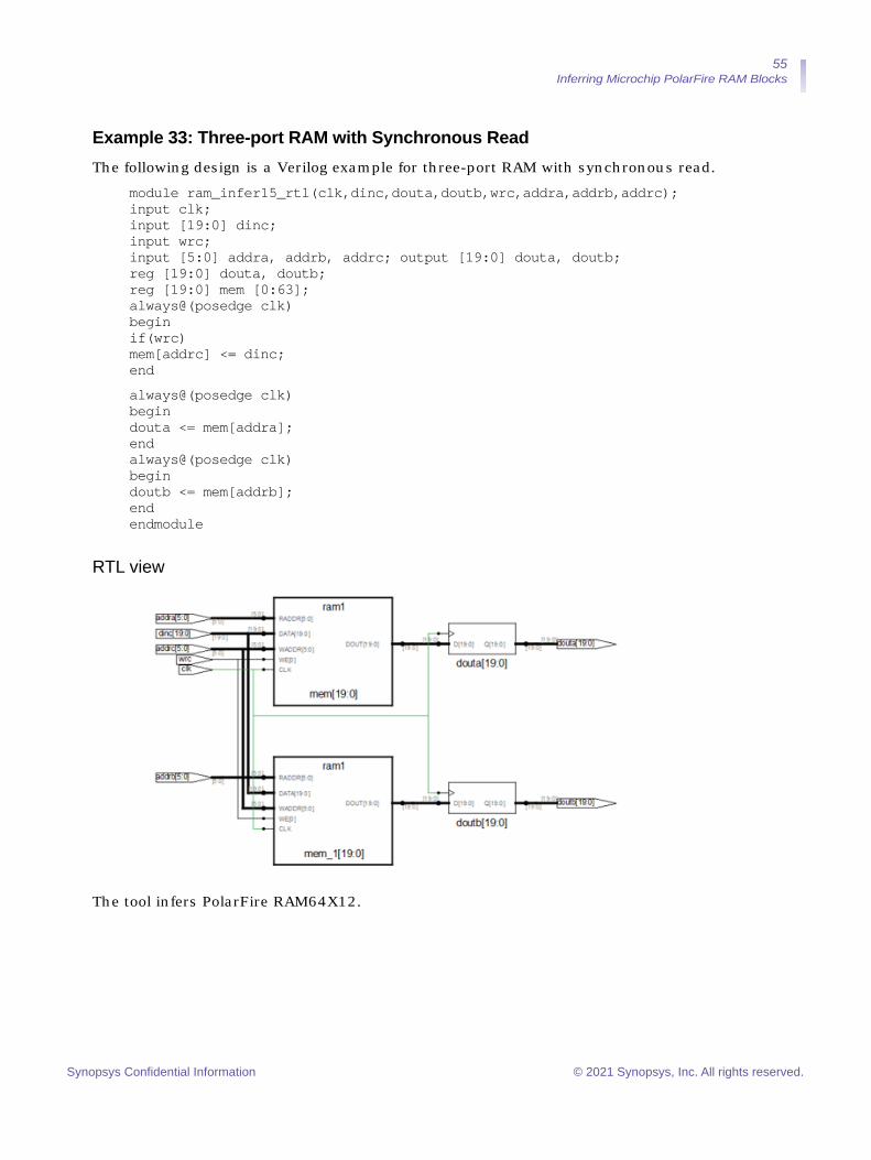
• Example 33: Three-port RAM with Synchronous Read, on page 55
• Example 34: Three-port RAM with Asynchronous Read, on page 56
• Example 35: Three-port RAM with read address and pipeline register, on page 57
• Example 36: Simple Dual-port RAM with enable on output register, on page 59
• Example 37: Single-port RAM with Asynchronous Reset (URAM), on page 60
• Example 38: Simple Dual-port URAM in Low Power Mode, on page 62
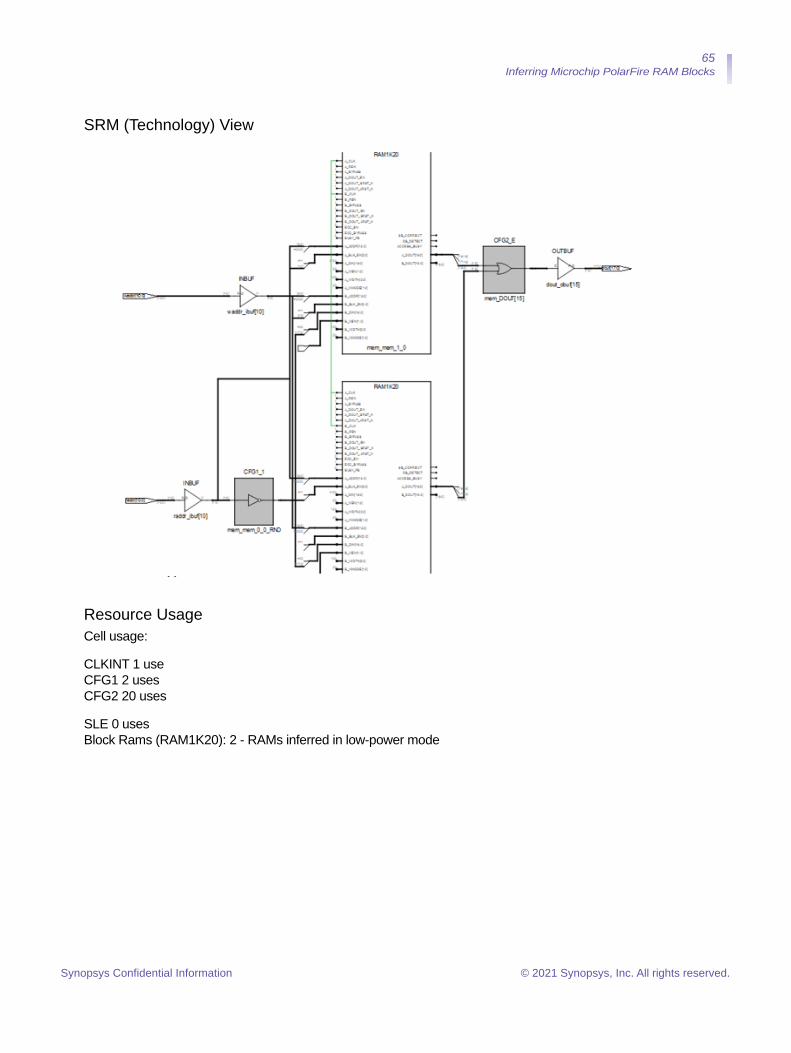
• Example 39: Simple Dual-port LSRAM in Low Power Mode, on page 64
• Example 40: Simple Dual-port PolarFire RAM with x1 configuration, on page 66
• Example 41: Single-port PolarFire RAM (VHDL), on page 68
• Example 42: PolarFire RAM with Enable on Output Register, on page 70
• Example 43: Asymmetric RAM with write_width > read_width using Output Register, on page 72
• Example 44: Asymmetric RAM with write_width < read_width using Output Register, on page 73
• Example 45: Asymmetric RAM with write_width > read_width; No change mode, on page 75
• Example 46: Asymmetric RAM with write_width < read_width; No change mode, on page 77
• Example 47: Asymmetric RAM with write_width > read_width; write-first mode, on page 79
• Example 48: Asymmetric RAM with write_width < read_width with Output Register; Write-first mode, on page 80
• Example 49: Asymmetric RAM with write_width > read_width; Read-first mode, on page 82
• Example 50: Asymmetric RAM with write_width < read_width with Output Register, on page 84
• Example 51: Asymmetric RAM with write_width>read_width with Output Register having Active High Asynchronous Reset, on page 86
• Example 52: Asymmetric RAM with write_width<read_width with Read address Register having Active High Asynchronous Reset, on page 88
• Example 53: Asymmetric RAM with write_width > read_width with Pipeline Register & Output Register having Enable, on page 90
• Example 54: Asymmetric RAM with write_width<read_width with Pipeline Register & Output Register having Enable, on page 92
Synopsys Confidential Information © 2021 Synopsys, Inc. All rights reserved.

11 Inferring Microchip PolarFire RAM Blocks
• Example 55: Asymmetric RAM with write_width > read_width with Pipeline Register and Output Register having Active high Synchronous Reset, on page 94
• Example 56: Asymmetric RAM with write_width < read_width with Pipeline Register & Output Register having Active High Synchronous Reset, on page 96
• Example 57: Asymmetric RAM with write_width > read_width using Pipeline Register & Output Register with Synchronous Reset, on page 99
• Example 58: VHDL Coding Style for Asymmetric RAM Inference for write_width > read_width, on page 101
• Example 59: VHDL Coding Style for Asymmetric RAM Inference for write_width < read_width, on page 102
• Example 60: Multi dimensional RAM inference, on page 104
Example 1: Single-port RAM - LSRAM (write-first mode)The following design is a single-port RAM with synchronous read and write operation. The same address is used for read and write operations in the write-first mode.
module ram_singleport_addreg (clk,wr,addr,din,dout); input clk; input [19:0] din; input wr; input [9:0] addr; output [19:0] dout;reg [9:0] addr_reg; reg [19:0] mem [0:1023] ; assign dout = mem[addr_reg]; always@(posedge clk)
begin addr_reg <= addr;
if(wr) mem[addr]<= din;
end endmodule
The synthesis tool infers PolarFire RAM1K20.
Synopsys Confidential Information © 2021 Synopsys, Inc. All rights reserved.
12 Inferring Microchip PolarFire RAM Blocks
Resource Usage Report for ram_singleport_addregThis section of the log file (.srr) shows resource usage details.
Mapping to part: pa5m300fbga896std
Block Rams (RAM1K20): 1
Sequential Cells: SLE 0 uses
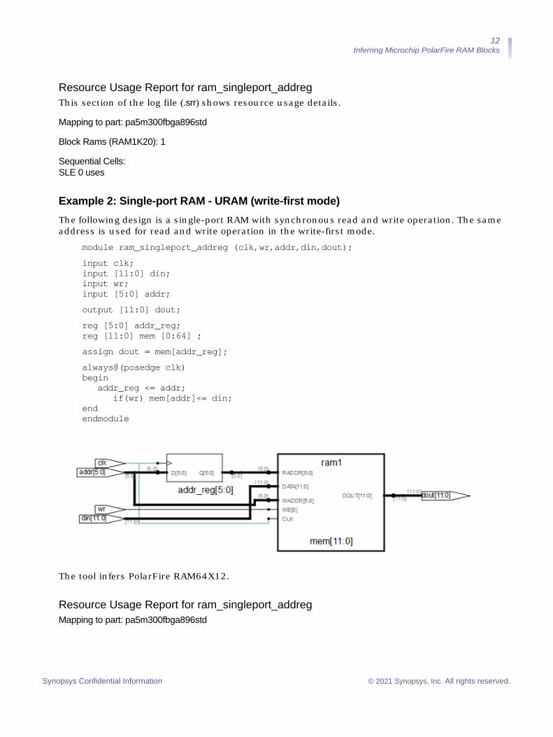
Example 2: Single-port RAM - URAM (write-first mode)The following design is a single-port RAM with synchronous read and write operation. The same address is used for read and write operation in the write-first mode.
module ram_singleport_addreg (clk,wr,addr,din,dout);input clk; input [11:0] din; input wr; input [5:0] addr;output [11:0] dout;reg [5:0] addr_reg; reg [11:0] mem [0:64] ;assign dout = mem[addr_reg];always@(posedge clk) begin
addr_reg <= addr; if(wr) mem[addr]<= din;
end endmodule
The tool infers PolarFire RAM64X12.
Resource Usage Report for ram_singleport_addregMapping to part: pa5m300fbga896std
Synopsys Confidential Information © 2021 Synopsys, Inc. All rights reserved.

13 Inferring Microchip PolarFire RAM Blocks
Cell usage: CLKINT 1 use RAM64x12 1 use
Sequential Cells: SLE 0 uses
Example 3: Single-port RAM with Pipeline Register - LSRAM (write-first mode)The following design is a single-port RAM with one pipeline register on the read port in the write-first mode.
module ram_singleport_pipereg (clk,we,addr,d,q);input [7:0] d; input [9:0] addr; input clk, we;reg [9:0] addr_reg; output reg [7:0] q;reg [7:0] mem [1023:0] ;always @(posedge clk) begin addr_reg <= addr; if(we) mem[addr] <= d; endalways @ (posedge clk ) beginq <= mem[addr_reg]; end endmodule
The tool infers PolarFire RAM1K20.
Synopsys Confidential Information © 2021 Synopsys, Inc. All rights reserved.

14 Inferring Microchip PolarFire RAM Blocks
Resource Usage Report for ram_singleport_piperegMapping to part: pa5m300fbga896std Cell usage: CLKINT 1 use RAM1K20 1 use
Sequential Cells: SLE 0 uses
Example 4: Single-port RAM with Pipeline Register - URAM (write-first mode)The following design is a single-port RAM with one pipeline register on the read port in the write-first mode.
module ram_singleport_pipereg(clk,we,addr,d,q);input [7:0] d; input [5:0] addr; input clk, we;reg [5:0] addr_reg; output reg [7:0] q;reg [7:0] mem [63:0] ;always @(posedge clk) begin addr_reg <= addr; if(we) mem[addr] <= d; endalways @ (posedge clk ) begin q <= mem[addr_reg]; end endmodule
The tool infers PolarFire RAM64X12.
Synopsys Confidential Information © 2021 Synopsys, Inc. All rights reserved.
15 Inferring Microchip PolarFire RAM Blocks
Resource Usage Report for ram_singleport_piperegMapping to part: pa5m300fbga896std
Cell usage: CLKINT 1 use RAM64x12 1 use
Sequential Cells: SLE 0 uses
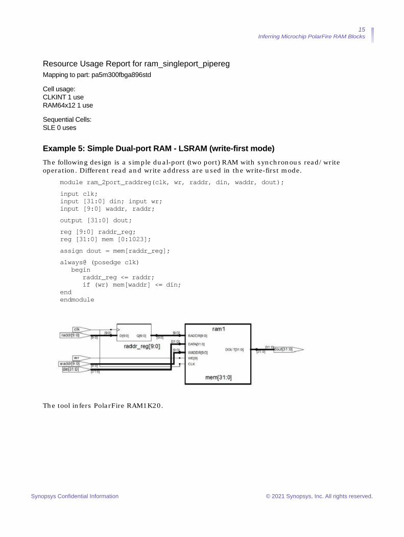
Example 5: Simple Dual-port RAM - LSRAM (write-first mode)The following design is a simple dual-port (two port) RAM with synchronous read/write operation. Different read and write address are used in the write-first mode.
module ram_2port_raddreg(clk, wr, raddr, din, waddr, dout);input clk; input [31:0] din; input wr; input [9:0] waddr, raddr;output [31:0] dout;reg [9:0] raddr_reg; reg [31:0] mem [0:1023];assign dout = mem[raddr_reg];always@ (posedge clk)
begin raddr_reg <= raddr; if (wr) mem[waddr] <= din;
end endmodule
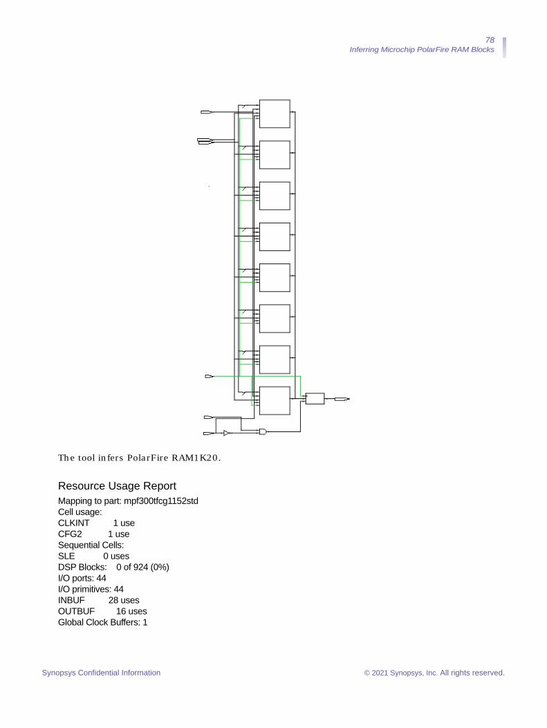
The tool infers PolarFire RAM1K20.
Synopsys Confidential Information © 2021 Synopsys, Inc. All rights reserved.

16 Inferring Microchip PolarFire RAM Blocks
Resource Usage Report for ram_2port_raddregMapping to part: pa5m300fbga896std Cell usage: CLKINT 1 use RAM1K20 2 uses
Sequential Cells: SLE 0 uses
Example 6: Simple Dual-port RAM - URAM (write-first mode)The following design is a simple dual-port (two port) RAM with synchronous read and write operation. Different read and write addresses are used in the write-first mode.
module ram_2port_raddreg(clk, wr, raddr, din, waddr, dout);input clk; input [11:0] din; input wr;input [5:0] waddr, raddr;output [11:0] dout;reg [5:0] raddr_reg; reg [11:0] mem [0:63];assign dout = mem[raddr_reg];always@(posedge clk) begin
raddr_reg <= raddr; if(wr) mem[waddr]<= din;
end endmodule
The tool infers PolarFire RAM64X12.
Synopsys Confidential Information © 2021 Synopsys, Inc. All rights reserved.

17 Inferring Microchip PolarFire RAM Blocks
Resource Usage Summary for ram_2port_raddregMapping to part: pa5m300fbga896std
Cell usage: CLKINT 1 use RAM64x12 1 use
Sequential Cells: SLE 0 uses
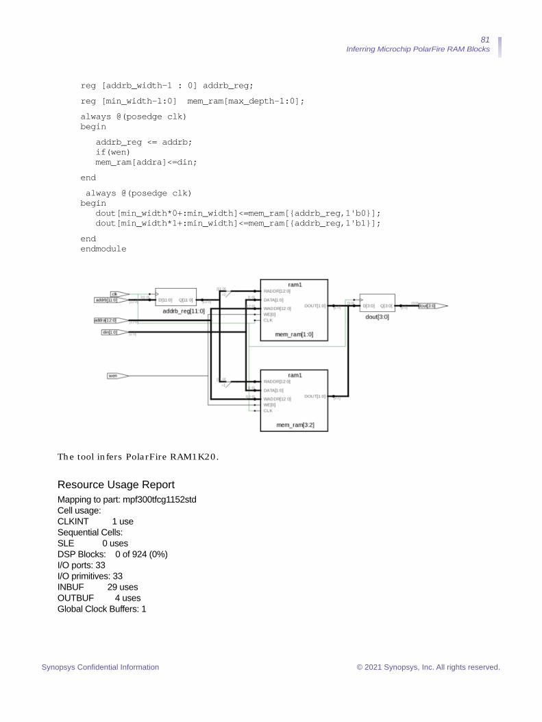
Example 7: Simple Dual-port RAM with Pipeline Register - LSRAM (write-first mode)The following design is a simple dual-port (two port) RAM with synchronous read and write operation with pipeline register in write-first mode.
module ram_2port_pipe(clk,wr,raddr,din,waddr,dout1);input clk; input [17:0] din; input wr; input [9:0] waddr,raddr;output [17:0] dout1 ; reg [9:0] raddr_reg; reg [17:0] mem [0:1023]; reg [17:0] dout, dout1;always@(posedge clk) begin
raddr_reg <= raddr; dout <= mem[raddr_reg];
if(wr) mem[waddr] <= din;
endalways @(posedge clk) begin
dout1 <= dout; endendmodule
The tool infers PolarFire RAM1K20.
Synopsys Confidential Information © 2021 Synopsys, Inc. All rights reserved.

18 Inferring Microchip PolarFire RAM Blocks
Note: The output pipeline register dout1 is not packed into the RAM. Only the register dout is packed in the RAM.
Resource Usage Report for ram_2port_pipeMapping to part: pa5m300fbga896std
Cell usage: CLKINT 1 use RAM1K20 1 use
Sequential Cells: SLE 18 uses
Example 8: Simple Dual-port RAM with Pipeline Register - URAM (write-first mode)The following design is a simple dual-port (two port) RAM with synchronous read and write operation with pipeline register in write-first mode.
module ram_2port_pipe(clk,wr,raddr,din,waddr,dout,rst);input clk; input [11:0] din; input wr, rst; input [5:0] waddr,raddr;output [11:0] dout;reg [5:0] raddr_reg; reg [11:0] mem [0:63];reg [11:0] dout2, dout; wire [11:0] dout1;assign dout1 = mem[raddr_reg];always@(posedge clk) begin
raddr_reg <= raddr; dout2 <= dout1; if(wr) mem[waddr] <= din;
endalways @(posedge clk or negedge rst) begin
if (~ rst ) dout <= 12'b0; else
dout <= dout2; end endmodule
Synopsys Confidential Information © 2021 Synopsys, Inc. All rights reserved.
19 Inferring Microchip PolarFire RAM Blocks
The tool infers PolarFire RAM64X12.
Note: The output pipeline register dout is not packed in the RAM.
Resource Usage Summary for ram_2port_pipeMapping to part: pa5m300fbga896std Cell usage: CLKINT 1 use RAM64x12 1 use
Sequential Cells: SLE 12 uses
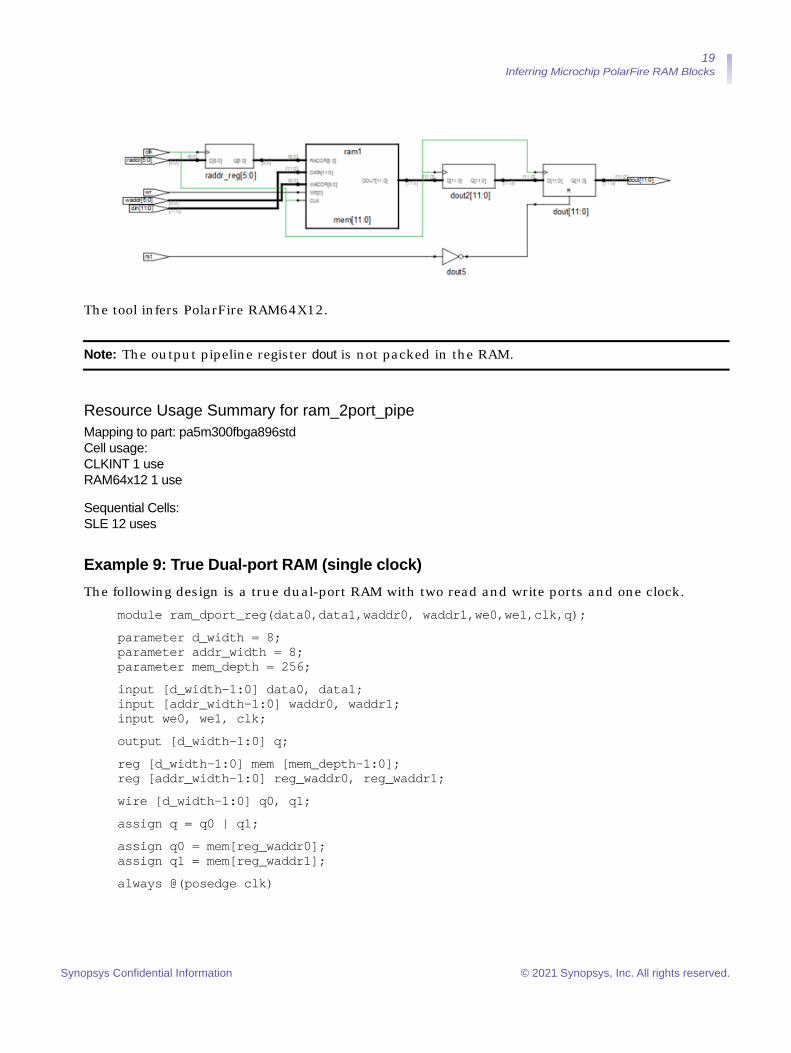
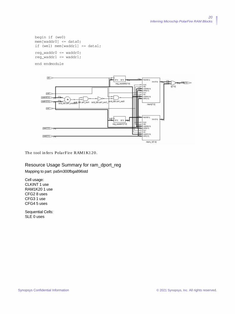
Example 9: True Dual-port RAM (single clock)The following design is a true dual-port RAM with two read and write ports and one clock.
module ram_dport_reg(data0,data1,waddr0, waddr1,we0,we1,clk,q);parameter d_width = 8; parameter addr_width = 8; parameter mem_depth = 256;input [d_width-1:0] data0, data1; input [addr_width-1:0] waddr0, waddr1; input we0, we1, clk;output [d_width-1:0] q;reg [d_width-1:0] mem [mem_depth-1:0]; reg [addr_width-1:0] reg_waddr0, reg_waddr1;wire [d_width-1:0] q0, q1;assign q = q0 | q1;assign q0 = mem[reg_waddr0]; assign q1 = mem[reg_waddr1];always @(posedge clk)
Synopsys Confidential Information © 2021 Synopsys, Inc. All rights reserved.
20 Inferring Microchip PolarFire RAM Blocks
begin if (we0) mem[waddr0] <= data0; if (we1) mem[waddr1] <= data1;reg_waddr0 <= waddr0; reg_waddr1 <= waddr1;end endmodule
The tool infers PolarFire RAM1K120.
Resource Usage Summary for ram_dport_regMapping to part: pa5m300fbga896std
Cell usage: CLKINT 1 use RAM1K20 1 use CFG2 8 uses CFG3 1 use CFG4 5 uses
Sequential Cells: SLE 0 uses
Synopsys Confidential Information © 2021 Synopsys, Inc. All rights reserved.
21 Inferring Microchip PolarFire RAM Blocks
Example 10: True Dual-port RAM (multiple clocks)The following design is a true dual-port RAM with two read and write ports and two clocks.
module test (clka,clkb,wea,addra,dataina,qa,web,addrb,datainb,qb);parameter addr_width = 10; parameter data_width = 18; input clka,clkb,wea,web;input [data_width - 1 : 0] dataina,datainb; input [addr_width - 1 : 0] addra,addrb;output reg [data_width - 1 : 0] qa,qb;reg [addr_width - 1 : 0] addra_reg, addrb_reg; reg [data_width - 1 : 0] mem [(2**addr_width) - 1 : 0] ;always @ (posedge clka)
begin addra_reg <= addra; if(wea) mem[addra] <= dataina;
endalways @ (posedge clkb)
begin a ddrb_reg <= addrb;
if(web) mem[addrb] <= datainb;
endalways @ (posedge clka)
begin if(~wea) qa <= mem[addra_reg]; else qa <= dataina;
endalways @ (posedge clkb)
begin if(~web) qb <= mem[addrb_reg]; else qb <= datainb;
endendmodule
Synopsys Confidential Information © 2021 Synopsys, Inc. All rights reserved.

22 Inferring Microchip PolarFire RAM Blocks
The tool infers PolarFire RAM1K20 with output registers qa and qb inferred outside the RAM using SLE's.
Resource Usage Summary for testMapping to part: pa5m300fbga896std
Cell usage: CLKINT 2 use RAM1K20 1 use CFG3 36 uses
Sequential Cells: SLE 36 uses
Example 11: True Dual-port RAM with Pipeline RegisterThe following design is a true dual-port RAM with two read and write ports and one clock with one pipeline register.
module ram_dport_reg(data0,data1,waddr0, waddr1,we0,we1,clk,q0, q1);parameter d_width = 8; parameter addr_width = 8; parameter mem_depth = 256;input [d_width-1:0] data0, data1; input [addr_width-1:0] waddr0, waddr1; input we0, we1, clk;output [d_width-1:0] q0, q1;
Synopsys Confidential Information © 2021 Synopsys, Inc. All rights reserved.

23 Inferring Microchip PolarFire RAM Blocks
reg [d_width-1:0] mem [mem_depth-1:0] ; reg [addr_width-1:0] reg_waddr0, reg_waddr1; reg [d_width-1:0] q;reg [d_width-1:0] q0, q1;always @(posedge clk) begin if (we0) mem[waddr0] <= data0; if (we1) mem[waddr1] <= data1;reg_waddr0 <= waddr0; reg_waddr1 <= waddr1;endalways @ (posedge clk) begin
q0 <= mem[reg_waddr0]; q1 <= mem[reg_waddr1];
end endmodule
The tool infers PolarFire RAM1K20.
Synopsys Confidential Information © 2021 Synopsys, Inc. All rights reserved.
24 Inferring Microchip PolarFire RAM Blocks
Resource UsageMapping to part: pa5m300fbga896std
Cell usage: CLKINT 1 use RAM1K20 1 use CFG3 7 uses CFG4 21 uses
Sequential Cells: SLE 36 uses
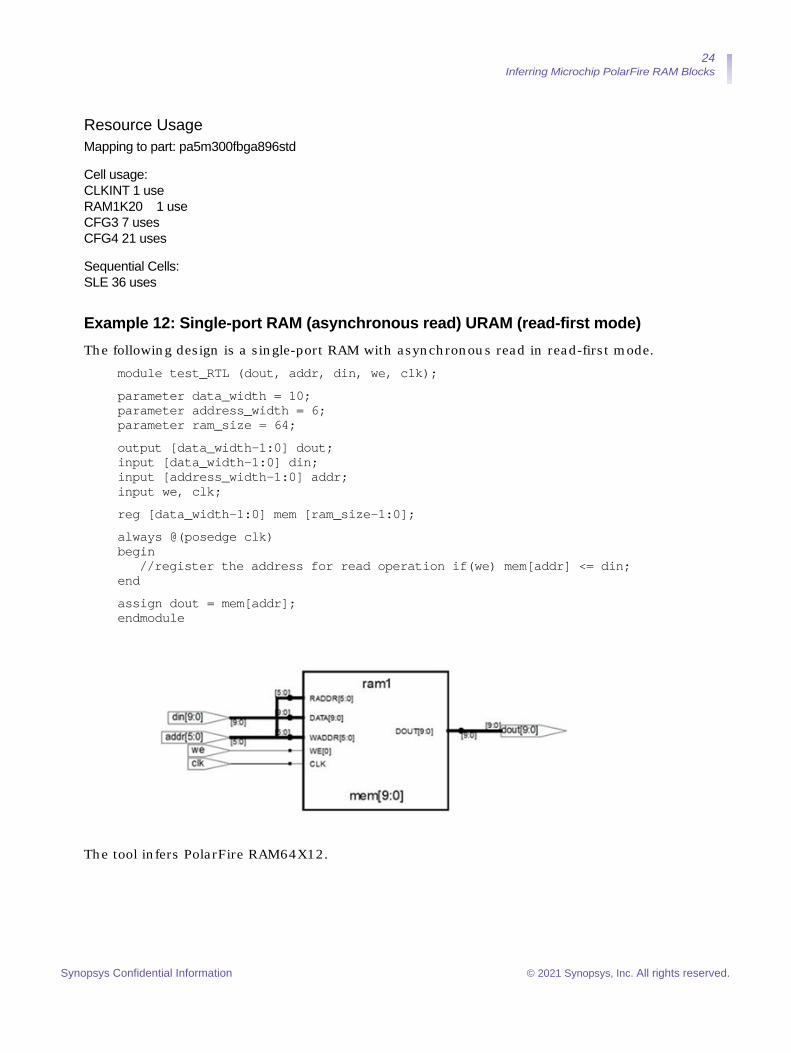
Example 12: Single-port RAM (asynchronous read) URAM (read-first mode)The following design is a single-port RAM with asynchronous read in read-first mode.
module test_RTL (dout, addr, din, we, clk);parameter data_width = 10; parameter address_width = 6; parameter ram_size = 64;output [data_width-1:0] dout; input [data_width-1:0] din; input [address_width-1:0] addr; input we, clk;reg [data_width-1:0] mem [ram_size-1:0];always @(posedge clk) begin
//register the address for read operation if(we) mem[addr] <= din; endassign dout = mem[addr]; endmodule
The tool infers PolarFire RAM64X12.
Synopsys Confidential Information © 2021 Synopsys, Inc. All rights reserved.
25 Inferring Microchip PolarFire RAM Blocks
Resource UsageMapping to part: pa5m300fbga896std Cell usage: RAM64x12 1 use Sequential Cells: SLE 0 uses
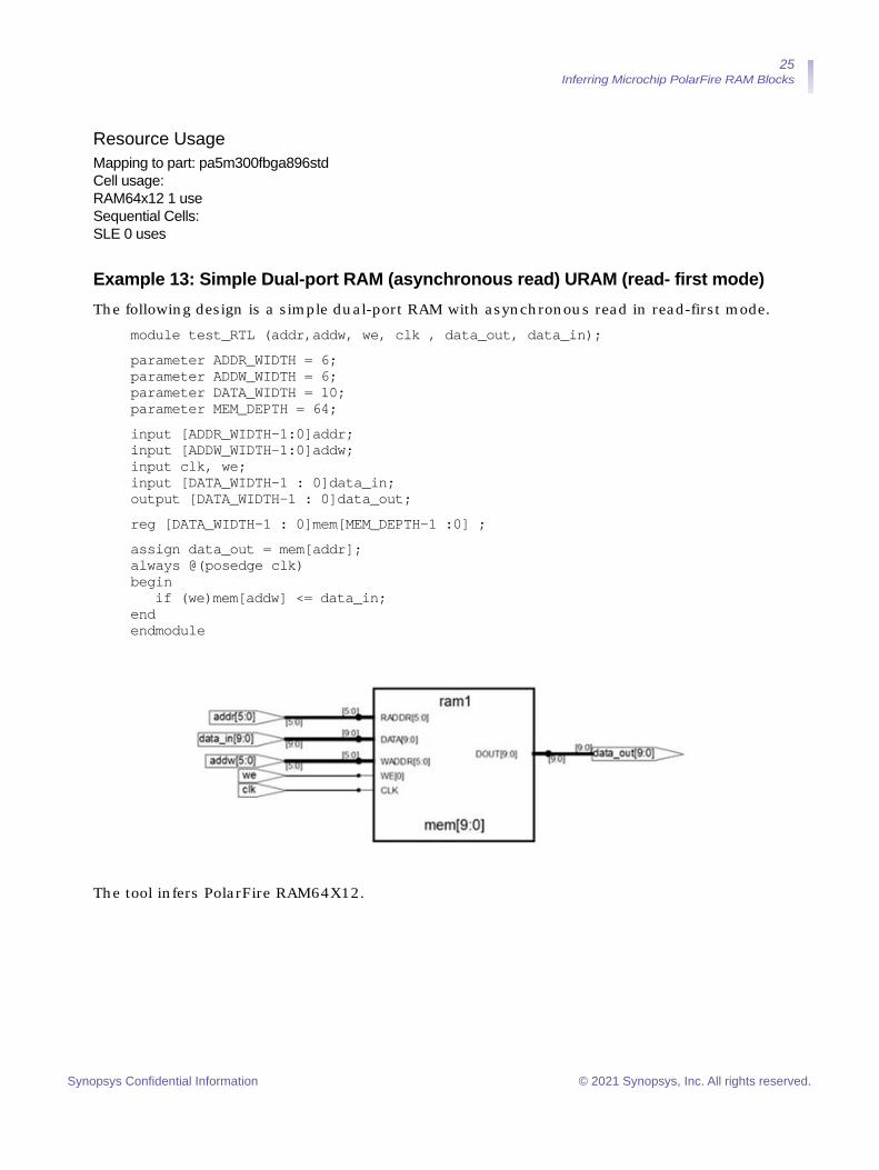
Example 13: Simple Dual-port RAM (asynchronous read) URAM (read- first mode)The following design is a simple dual-port RAM with asynchronous read in read-first mode.
module test_RTL (addr,addw, we, clk , data_out, data_in);parameter ADDR_WIDTH = 6; parameter ADDW_WIDTH = 6; parameter DATA_WIDTH = 10; parameter MEM_DEPTH = 64;input [ADDR_WIDTH-1:0]addr; input [ADDW_WIDTH-1:0]addw; input clk, we; input [DATA_WIDTH-1 : 0]data_in; output [DATA_WIDTH-1 : 0]data_out;reg [DATA_WIDTH-1 : 0]mem[MEM_DEPTH-1 :0] ;assign data_out = mem[addr]; always @(posedge clk) begin
if (we)mem[addw] <= data_in; end endmodule
The tool infers PolarFire RAM64X12.
Synopsys Confidential Information © 2021 Synopsys, Inc. All rights reserved.
26 Inferring Microchip PolarFire RAM Blocks
Resource UsageMapping to part: pa5m300fbga896std
Cell usage: RAM64x12 1 use
Sequential Cells: SLE 0 uses
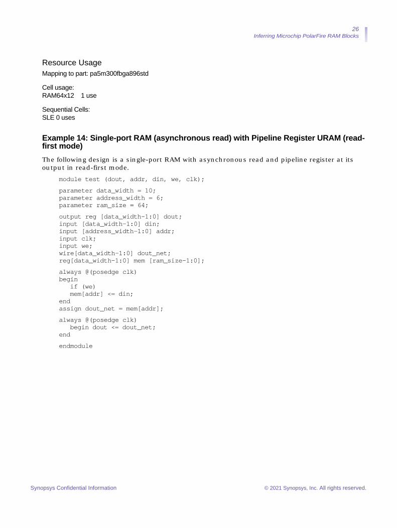
Example 14: Single-port RAM (asynchronous read) with Pipeline Register URAM (read-first mode)The following design is a single-port RAM with asynchronous read and pipeline register at its output in read-first mode.
module test (dout, addr, din, we, clk);parameter data_width = 10; parameter address_width = 6; parameter ram_size = 64;output reg [data_width-1:0] dout; input [data_width-1:0] din; input [address_width-1:0] addr; input clk; input we; wire[data_width-1:0] dout_net; reg[data_width-1:0] mem [ram_size-1:0];always @(posedge clk) begin
if (we) mem[addr] <= din;
end assign dout_net = mem[addr];always @(posedge clk)
begin dout <= dout_net; endendmodule
Synopsys Confidential Information © 2021 Synopsys, Inc. All rights reserved.
27 Inferring Microchip PolarFire RAM Blocks
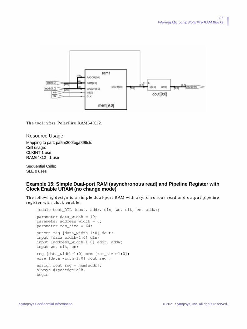
The tool infers PolarFire RAM64X12.
Resource UsageMapping to part: pa5m300fbga896std Cell usage: CLKINT 1 use RAM64x12 1 use
Sequential Cells: SLE 0 uses
Example 15: Simple Dual-port RAM (asynchronous read) and Pipeline Register with Clock Enable URAM (no change mode)The following design is a simple dual-port RAM with asynchronous read and output pipeline register with clock enable.
module test_RTL (dout, addr, din, we, clk, en, addw);parameter data_width = 10; parameter address_width = 6; parameter ram_size = 64;output reg [data_width-1:0] dout; input [data_width-1:0] din; input [address_width-1:0] addr, addw; input we, clk, en;reg [data_width-1:0] mem [ram_size-1:0]; wire [data_width-1:0] dout_reg ;assign dout_reg = mem[addr]; always @(posedge clk) begin
Synopsys Confidential Information © 2021 Synopsys, Inc. All rights reserved.
28 Inferring Microchip PolarFire RAM Blocks
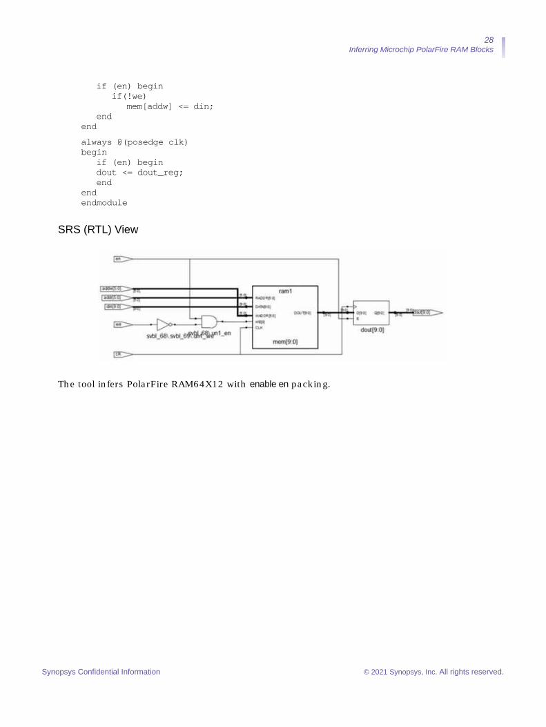
if (en) begin if(!we)
mem[addw] <= din; end
endalways @(posedge clk) begin
if (en) begin dout <= dout_reg; end
end endmodule
SRS (RTL) View
The tool infers PolarFire RAM64X12 with enable en packing.
Synopsys Confidential Information © 2021 Synopsys, Inc. All rights reserved.

29 Inferring Microchip PolarFire RAM Blocks
SRM (Technology) View
Resource UsageMapping to part: pa5m300fbga896std
Cell usage: CLKINT 1 use RAM64x12 1 use CFG2 1 use
Sequential Cells: SLE 0 uses
Synopsys Confidential Information © 2021 Synopsys, Inc. All rights reserved.
30 Inferring Microchip PolarFire RAM Blocks
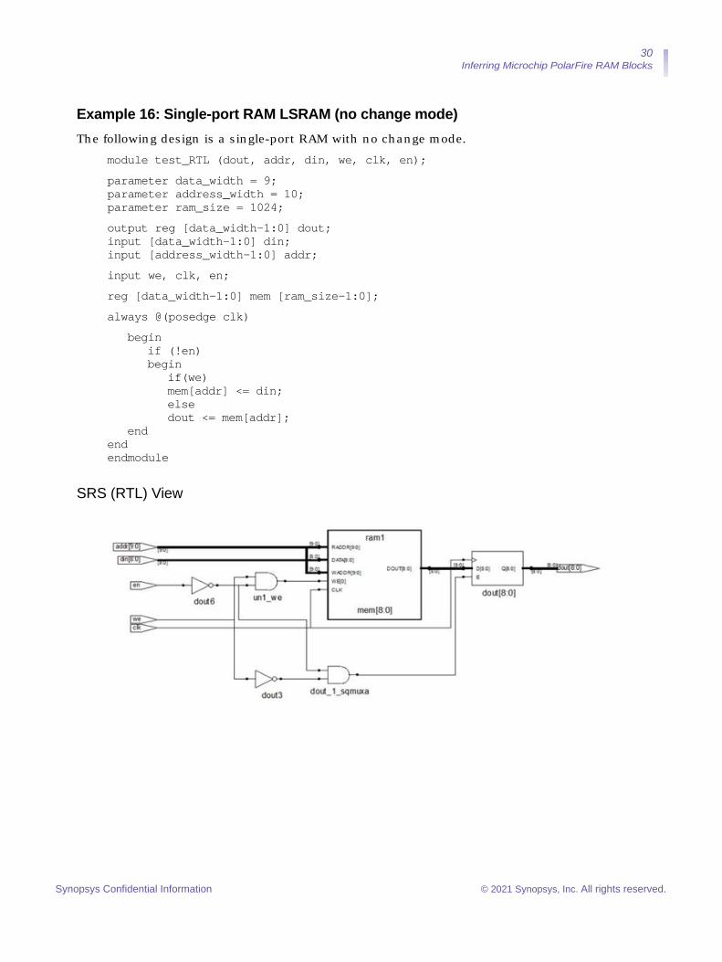
Example 16: Single-port RAM LSRAM (no change mode)The following design is a single-port RAM with no change mode.
module test_RTL (dout, addr, din, we, clk, en);parameter data_width = 9; parameter address_width = 10; parameter ram_size = 1024;output reg [data_width-1:0] dout; input [data_width-1:0] din; input [address_width-1:0] addr;input we, clk, en;reg [data_width-1:0] mem [ram_size-1:0];always @(posedge clk)
begin if (!en) begin
if(we) mem[addr] <= din; else dout <= mem[addr];
end end endmodule
SRS (RTL) View
Synopsys Confidential Information © 2021 Synopsys, Inc. All rights reserved.
31 Inferring Microchip PolarFire RAM Blocks
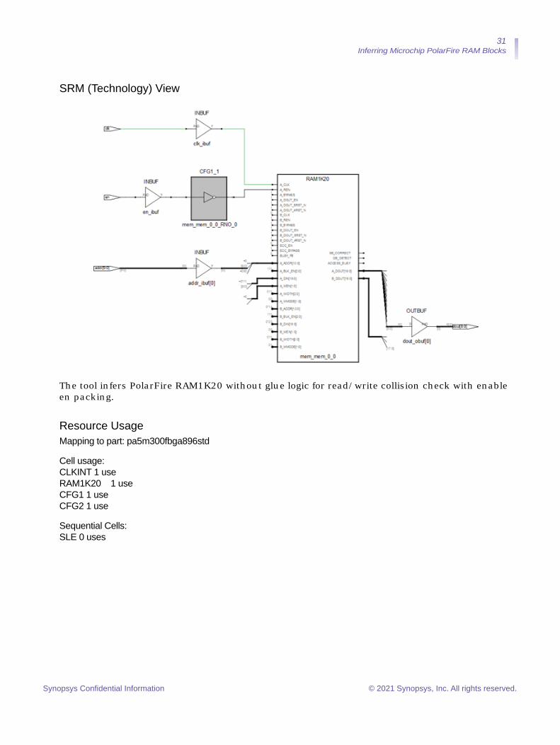
SRM (Technology) View
The tool infers PolarFire RAM1K20 without glue logic for read/write collision check with enable en packing.
Resource UsageMapping to part: pa5m300fbga896std
Cell usage: CLKINT 1 use RAM1K20 1 use CFG1 1 use CFG2 1 use
Sequential Cells: SLE 0 uses
Synopsys Confidential Information © 2021 Synopsys, Inc. All rights reserved.

32 Inferring Microchip PolarFire RAM Blocks
Example 17: Single-port RAM with One Pipelined Register on the Read Port (sync-sync) (no change mode)The following design is a single-port RAM with one pipeline register on the read port using no change mode.
module ram_singleport_pipereg(clk,we,a,d,q1);input [7:0] d; input [7:0] a; input clk, we;reg [7:0] q; output [7:0] q1; reg [7:0] q1; reg [7:0] mem [255:0];always @(posedge clk)
begin if(we)
mem[a] <= d; else q <= mem[a]; end
always @ (posedge clk) begin q1 <= q; end
endmodule
The tool infers PolarFire RAM1K20.
Synopsys Confidential Information © 2021 Synopsys, Inc. All rights reserved.
33 Inferring Microchip PolarFire RAM Blocks
Resource UsageMapping to part: pa5m300fbga896std
Cell usage: RAM1K20 1
Sequential Cells: SLE 0 uses
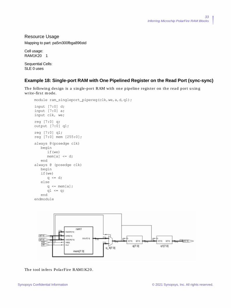
Example 18: Single-port RAM with One Pipelined Register on the Read Port (sync-sync)The following design is a single-port RAM with one pipeline register on the read port using write-first mode.
module ram_singleport_pipereg(clk,we,a,d,q1);input [7:0] d; input [7:0] a; input clk, we;reg [7:0] q; output [7:0] q1;reg [7:0] q1; reg [7:0] mem [255:0];always @(posedge clk)
begin if(we) mem[a] <= d;
end always @ (posedge clk)
begin if(we)
q <= d; else
q <= mem[a]; q1 <= q;
end endmodule
The tool infers PolarFire RAM1K20.
Synopsys Confidential Information © 2021 Synopsys, Inc. All rights reserved.
34 Inferring Microchip PolarFire RAM Blocks
Resource UsageMapping to part: pa5m300fbga896std
Cell usage: CLKINT 1 use RAM1K20 1 use
Sequential Cells: SLE 0 uses
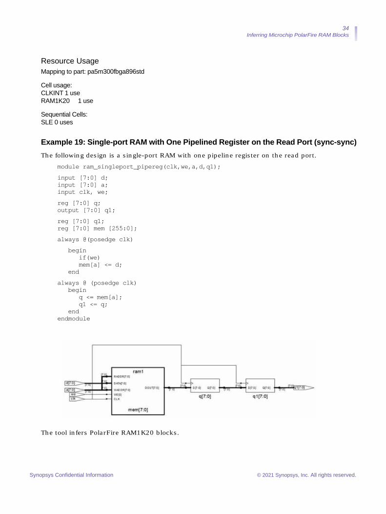
Example 19: Single-port RAM with One Pipelined Register on the Read Port (sync-sync)The following design is a single-port RAM with one pipeline register on the read port.
module ram_singleport_pipereg(clk,we,a,d,q1);input [7:0] d; input [7:0] a; input clk, we;reg [7:0] q; output [7:0] q1;reg [7:0] q1; reg [7:0] mem [255:0];always @(posedge clk)
begin if(we) mem[a] <= d;
endalways @ (posedge clk)
begin q <= mem[a]; q1 <= q;
end endmodule
The tool infers PolarFire RAM1K20 blocks.
Synopsys Confidential Information © 2021 Synopsys, Inc. All rights reserved.
35 Inferring Microchip PolarFire RAM Blocks
Resource UsageMapping to part: pa5m300fbga896std
Cell usage: CLKINT 1 use RAM1K20 1
Sequential Cells: SLE 0 uses
Example 20: Single-port RAM with Synchronous Read Without Pipeline Register (sync-async) (no change mode)The following design is a single-port RAM with synchronous read without pipeline register using no change mode.
module ram_singleport_pipereg(clk,we,a,d,q); input [7:0] d; input [7:0] a; input clk, we; output [7:0] q; reg [7:0] q; reg [7:0] mem [255:0];always @(posedge clk)
begin if(~we) mem[a] <= d; else q <= mem[a];
end endmodule
The tool infers PolarFire RAM1K20 along with logic for no change mode with enable en packing.
Synopsys Confidential Information © 2021 Synopsys, Inc. All rights reserved.
36 Inferring Microchip PolarFire RAM Blocks
Resource UsageMapping to part: pa5m300fbga896std
Cell usage: CLKINT 1 use RAM1K20 1 CFG1 1 use
Sequential Cells: SLE 0 uses
Example 21: Simple-dual Port RAM with Output RegisterThe following design is a single-port RAM with output register.
module ram_2port_pipe(clk,wr,raddr,din,waddr,dout);input clk; input [17:0] din; input wr; input [9:0] waddr,raddr;output [17:0] dout;reg [9:0] raddr_reg; reg [17:0 mem [0:1023]; reg [17:0] dout;always@(posedge clk)
begin raddr_reg <= raddr; dout <= mem[raddr_reg]; if(wr) mem[waddr]<= din;
end endmodule
The tool infers PolarFire RAM1K20.
Synopsys Confidential Information © 2021 Synopsys, Inc. All rights reserved.
37 Inferring Microchip PolarFire RAM Blocks
Resource UsageMapping to part: pa5m300fbga896std
Cell usage: CLKINT 1 use RAM1K20 1 use
Sequential Cells: SLE 0 uses
Example 22: Single-port RAM with Output Registers (VHDL)The following design is a single-port RAM with output registers.
library ieee; use ieee.std_logic_1164.all; use ieee.std_logic_unsigned.all; entity ram_singleport_outreg is port (d: in std_logic_vector(7 downto 0);
a: in integer range 127 downto 0; we: in std_logic; clk: in std_logic; q: out std_logic_vector(7 downto 0) ); end ram_singleport_outreg;
architecture rtl of ram_singleport_outreg is type mem_type is array (127 downto 0) of std_logic_vector (7 downto 0); signal mem: mem_type; begin
process(clk) begin
if (clk'event and clk='1') then q <= mem(a); if (we='1') then mem(a) <= d;
end if; end if; end process; end rtl;
Synopsys Confidential Information © 2021 Synopsys, Inc. All rights reserved.
38 Inferring Microchip PolarFire RAM Blocks
The tool infers PolarFire RAM64X12.
Resource UsageMapping to part: pa5m300fbga896std
Cell usage: CLKINT 1 use RAM64x12 2 uses
Sequential Cells: SLE 1 use
Example 23: Single Port RAM with Asynchronous Read (VHDL)The following design is a single-port RAM with asynchronous read.
library ieee; use ieee.std_logic_1164.all; use ieee.std_logic_unsigned.all; entity ram_singleport_noreg is
port (d : in std_logic_vector(7 downto 0); a : in std_logic_vector(6 downto 0); we : in std_logic; clk : in std_logic; q : out std_logic_vector(7 downto 0) ); end ram_singleport_noreg;
architecture rtl of ram_singleport_noreg is type mem_type is array (127 downto 0) of
std_logic_vector (7 downto 0); signal mem: mem_type; begin process
Synopsys Confidential Information © 2021 Synopsys, Inc. All rights reserved.

39 Inferring Microchip PolarFire RAM Blocks
(clk) begin
if rising_edge(clk) then if (we = '1') then mem(conv_integer (a)) <= d;
end if; end if;
end process; q <= mem(conv_integer (a)); end rtl;
The tool infers PolarFire RAM64X12.
Resource UsageMapping to part: pa5m300fbga896std
Cell usage: RAM64x12 2 uses
Sequential Cells: SLE 0 uses
Synopsys Confidential Information © 2021 Synopsys, Inc. All rights reserved.

40 Inferring Microchip PolarFire RAM Blocks
Example 24: Simple Dual-port RAM with Output Register and Read Address Register (VHDL)The following design is a simple dual-port RAM with output and read address registers.
library ieee; use ieee.std_logic_1164.all; use ieee.std_logic_unsigned.all;entity ram_simpledualport_outreg is
port (d: in std_logic_vector(7 downto 0); addr: in integer range 1023 downto 0; addw: in integer range 1023 downto 0; we: in std_logic; clk: in std_logic; q: out std_logic_vector(7 downto 0) );
end ram_simpledualport_outreg;architecture rtl of ram_simpledualport_outreg is type mem_type is array (1023 downto 0) of std_logic_vector (7 downto 0); signal mem: mem_type; signal a_reg : integer range 1023 downto 0; beginprocess (clk)
begin if (clk'event and clk='1' ) then a_reg <= addr; end if;
end process;process(clk)
begin if (clk'event and clk='1')
then q <= mem(a_reg); if (we='1') then mem(addw) <= d; end if;
end if; end process;
end rtl;
The tool infers PolarFire RAM1K20.
Synopsys Confidential Information © 2021 Synopsys, Inc. All rights reserved.
41 Inferring Microchip PolarFire RAM Blocks
Resource UsageMapping to part: pa5m300fbga896std
Cell usage: CLKINT 1 use RAM1K20 1 use
Sequential Cells: SLE 0 uses
Example 25: True Dual-port RAM with Read Address Register (VHDL)The following design is a true dual-port RAM with read address register.
library ieee; use ieee.std_logic_1164.all; use ieee.numeric_std.all; entity ram_dp_reg is generic (data_width : integer := 4; address_width :integer := 5 ); port (data_a:in std_logic_vector(data_width-1 downto 0); data_b:in std_logic_vector(data_width-1 downto 0); addr_a:in std_logic_vector(address_width-1 downto 0); addr_b:in std_logic_vector(address_width-1 downto 0); wren_a:in std_logic; wren_b:in std_logic; clk:in std_logic; q_a:out std_logic_vector(data_width-1 downto 0); q_b:out std_logic_vector(data_width-1 downto 0) ); end ram_dp_reg;architecture rtl of ram_dp_reg is type mem_array is array(0 to 2**(address_width) -1) of std_logic_vector(data_width-1 downto 0); signal mem : mem_array;signal addr_a_reg : std_logic_vector(address_width-1 downto 0); signal addr_b_reg : std_logic_vector(address_width-1 downto 0); begin
WRITE_RAM : process (clk) begin if rising_edge(clk) then if (wren_a = '1') then
mem(to_integer(unsigned(addr_a))) <= data_a; end if; if (wren_b='1') then mem(to_integer(unsigned(addr_b))) <= data_b; end if;
addr_a_reg <= addr_a; addr_b_reg <= addr_b;
end if; end process WRITE_RAM;q_a <= mem(to_integer(unsigned(addr_a_reg))); q_b <= mem(to_integer(unsigned(addr_b_reg)));end rtl;
Synopsys Confidential Information © 2021 Synopsys, Inc. All rights reserved.

42 Inferring Microchip PolarFire RAM Blocks
The tool infers PolarFire RAM1K20.
Resource UsageMapping to part: pa5m300fbga896std
Cell usage: CLKINT 1 use RAM1K20 1 use CFG3 1 use CFG4 3 uses
Sequential Cells: SLE 0 uses
Example 26: Simple Dual-port (two-port) RAM with Read Address Register (512 x 40 configurations)The following design is a simple dual-port RAM with read address register.
module ram_2port_addreg_512x40(clk,wr,raddr,din,waddr,dout);input clk; input [39:0] din; input wr; input [6:0] waddr,raddr;output [39:0] dout;reg [6:0] raddr_reg; reg [39:0] mem [0:511]; wire [39:0] dout;assign dout = mem[raddr_reg];
Synopsys Confidential Information © 2021 Synopsys, Inc. All rights reserved.
43 Inferring Microchip PolarFire RAM Blocks
always@(posedge clk) begin raddr_reg <= raddr; if(wr) mem[waddr]<= din;
end endmodule
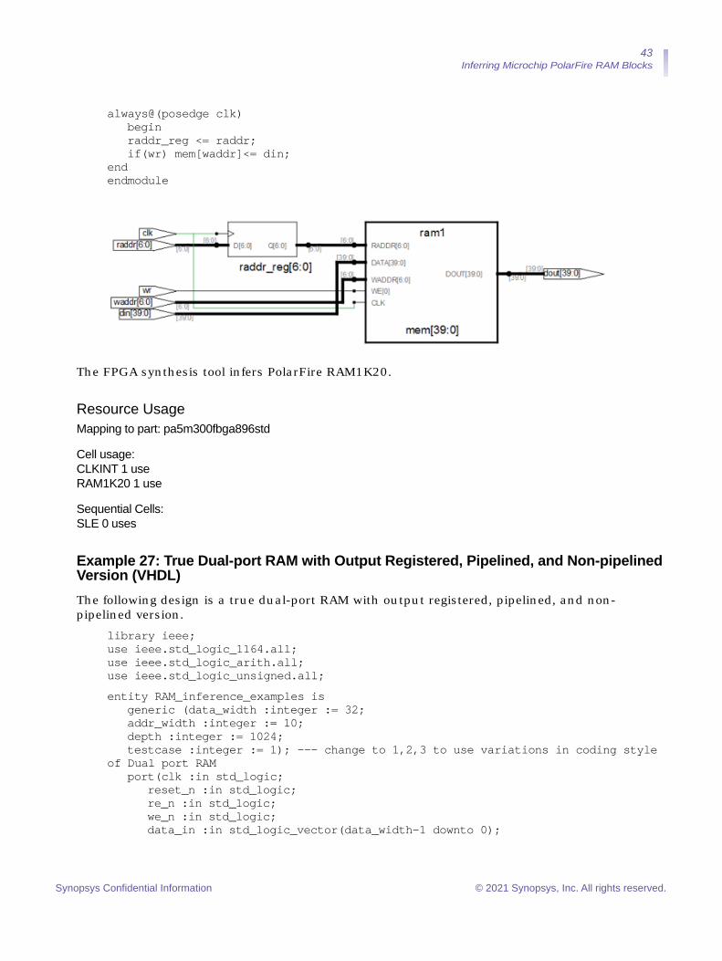
The FPGA synthesis tool infers PolarFire RAM1K20.
Resource UsageMapping to part: pa5m300fbga896std
Cell usage: CLKINT 1 use RAM1K20 1 use
Sequential Cells: SLE 0 uses
Example 27: True Dual-port RAM with Output Registered, Pipelined, and Non-pipelined Version (VHDL)The following design is a true dual-port RAM with output registered, pipelined, and non-pipelined version.
library ieee; use ieee.std_logic_1164.all; use ieee.std_logic_arith.all; use ieee.std_logic_unsigned.all;entity RAM_inference_examples is
generic (data_width :integer := 32; addr_width :integer := 10; depth :integer := 1024; testcase :integer := 1); --- change to 1,2,3 to use variations in coding style
of Dual port RAM port(clk :in std_logic;
reset_n :in std_logic; re_n :in std_logic; we_n :in std_logic; data_in :in std_logic_vector(data_width-1 downto 0);
Synopsys Confidential Information © 2021 Synopsys, Inc. All rights reserved.
44 Inferring Microchip PolarFire RAM Blocks
data_out :out std_logic_vector(data_width-1 downto 0); addr_0 :in std_logic_vector(addr_width-1 downto 0); addr_1 :in std_logic_vector(addr_width-1 downto 0); r_wen_0 :in std_logic; r_wen_1 :in std_logic;data_in_0 :in std_logic_vector(data_width-1 downto 0); data_out_0 :out std_logic_vector(data_width-1 downto 0); data_in_1 : in std_logic_vector(data_width-1 downto 0); data_out_1 :out std_logic_vector(data_width-1 downto 0)
); end RAM_inference_examples;architecture DEF_ARCH of RAM_inference_examples is type mem_type is array (depth-1 downto 0) of std_logic_vector (data_width-1 downto 0); signal BRAM_store :mem_type; signal int_addr_0 :integer range 0 to 4096; signal int_addr_1 :integer range 0 to 4096; signal rd_addr :integer range 0 to 4096; signal wr_addr :integer range 0 to 4096; signal data_out_tmp :std_logic_vector(data_width-1 downto 0); signal data_out_0tmp :std_logic_vector(data_width-1 downto 0); signal data_out_1tmp :std_logic_vector(data_width-1 downto 0); begin
Case 1 - Dual-port without pipelining (registered data_out ports)case_num1 : if testcase = 1 generateint_addr_0 <= CONV_INTEGER(addr_0); int_addr_1 <= CONV_INTEGER(addr_1);process(clk) begin
if rising_edge(clk) then -- port 0
if (r_wen_0 = '0') then BRAM_store(int_addr_0) <= data_in_0;
else data_out_0 <= BRAM_store(int_addr_0);
end if; -- port 1
if (r_wen_1 = '0') then BRAM_store(int_addr_1) <= data_in_1;
else data_out_1 <= BRAM_store(int_addr_1); end if;
end if; end process;
end generate;
Synopsys Confidential Information © 2021 Synopsys, Inc. All rights reserved.
45 Inferring Microchip PolarFire RAM Blocks
Case 2 - Dual-port with pipelining (registered data_out ports)case_num2 : if testcase = 2 generate
int_addr_0 <= CONV_INTEGER(addr_0); int_addr_1 <= CONV_INTEGER(addr_1);
process(clk) begin
if rising_edge(clk) then -- port 0
if (r_wen_0 = '0') then BRAM_store(int_addr_0) <= data_in_0;
else data_out_0tmp <= BRAM_store(int_addr_0);
end if; -- port 1
if (r_wen_1 = '0') then BRAM_store(int_addr_1) <= data_in_1; else data_out_1tmp <= BRAM_store(int_addr_1); end if;data_out_0<= data_out_0tmp; data_out_1<= data_out_1tmp;
end if; end process;
end generate;--end def_arch;
Case 3 - Dual-port with pipelining (registered read address)case_num3 : if testcase = 3 generateprocess(clk) begin
if rising_edge(clk) then -- port 1
if (r_wen_0 = '0') then BRAM_store(int_addr_0) <= data_in_0;
else int_addr_0 <= CONV_INTEGER(addr_0);
end if; -- port 1
if (r_wen_1 = '0') then BRAM_store(int_addr_1) <= data_in_1;
else int_addr_1 <= CONV_INTEGER(addr_1);
end if;data_out_0 <= BRAM_store(int_addr_0); data_out_1 <= BRAM_store(int_addr_1);
end if; end process;
end generate;end def_arch;
Synopsys Confidential Information © 2021 Synopsys, Inc. All rights reserved.

46 Inferring Microchip PolarFire RAM Blocks
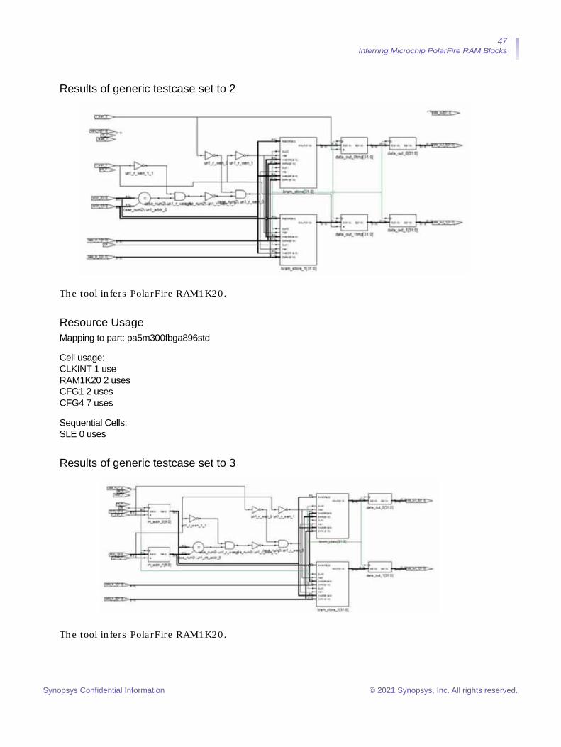
Results of generic testcase set to 1
The tool infers PolarFire RAM1K20.
Resource UsageMapping to part: pa5m300fbga896std
Cell usage: CLKINT 1 use RAM1K20 2 uses
CFG1 2 uses
CFG4 7 uses
Sequential Cells: SLE 0 uses
Synopsys Confidential Information © 2021 Synopsys, Inc. All rights reserved.
47 Inferring Microchip PolarFire RAM Blocks
Results of generic testcase set to 2
The tool infers PolarFire RAM1K20.
Resource UsageMapping to part: pa5m300fbga896std
Cell usage: CLKINT 1 use RAM1K20 2 uses CFG1 2 uses CFG4 7 uses
Sequential Cells: SLE 0 uses
Results of generic testcase set to 3
The tool infers PolarFire RAM1K20.
Synopsys Confidential Information © 2021 Synopsys, Inc. All rights reserved.
48 Inferring Microchip PolarFire RAM Blocks
Resource UsageMapping to part: pa5m300fbga896std
Cell usage: CLKINT 1 use RAM1K20 2 uses CFG1 2 uses CFG2 1 use CFG3 1 use CFG4 6 uses
Sequential Cells: SLE 20 uses
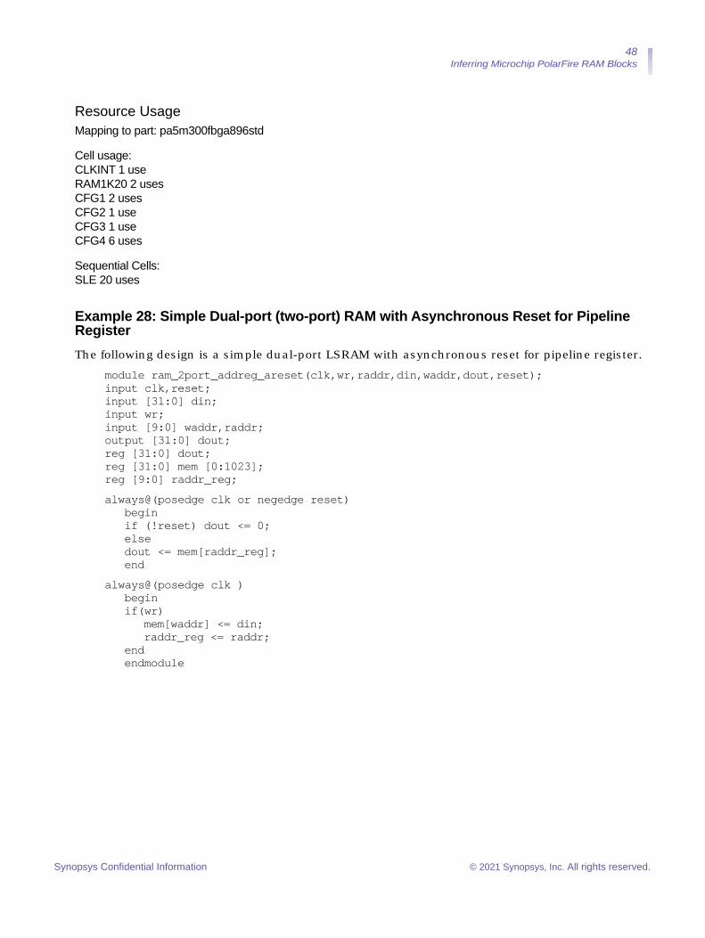
Example 28: Simple Dual-port (two-port) RAM with Asynchronous Reset for Pipeline RegisterThe following design is a simple dual-port LSRAM with asynchronous reset for pipeline register.
module ram_2port_addreg_areset(clk,wr,raddr,din,waddr,dout,reset); input clk,reset; input [31:0] din; input wr; input [9:0] waddr,raddr; output [31:0] dout; reg [31:0] dout; reg [31:0] mem [0:1023]; reg [9:0] raddr_reg;always@(posedge clk or negedge reset)
begin if (!reset) dout <= 0; else dout <= mem[raddr_reg]; end
always@(posedge clk ) begin if(wr)
mem[waddr] <= din; raddr_reg <= raddr;
end endmodule
Synopsys Confidential Information © 2021 Synopsys, Inc. All rights reserved.

49 Inferring Microchip PolarFire RAM Blocks
SRS (RTL) View
SRM (Technology) View
The tool infers PolarFire RAM1K20 with asynchronous reset packing.
Resource UsageMapping to part: pa5m300fbga896std
Cell usage: CLKINT 1 use RAM1K20 2 uses
Sequential Cells: SLE 0 uses
Synopsys Confidential Information © 2021 Synopsys, Inc. All rights reserved.

50 Inferring Microchip PolarFire RAM Blocks
Example 29: Single-port RAM with Synchronous Reset for Pipeline Register (LSRAM)The following design is a single-port RAM with synchronous reset for pipeline register.
module ram_singleport_writefirst_pipe_areset(clk,we,a,d,q1,reset); input [7:0] d; input [7:0] a;input clk, we,reset; reg [7:0] q; output [7:0] q1; reg [7:0] q1; reg [7:0] mem [255:0];always @(posedge clk) begin if(we) mem[a] <= d; endalways @ (posedge clk) begin if(we) q <= d; else q <= mem[a]; end always @ (posedge clk )
begin if (reset) q1 <= 0; else q1 <= q; end endmodule
The tool infers PolarFire RAM1K20.
Synopsys Confidential Information © 2021 Synopsys, Inc. All rights reserved.
51 Inferring Microchip PolarFire RAM Blocks
Resource UsageMapping to part: pa5m300fbga896std
Cell usage: CLKINT 1 use RAM1K20 1 use CFG1 1 use
Sequential Cells: SLE 0 uses
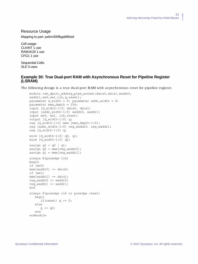
Example 30: True Dual-port RAM with Asynchronous Reset for Pipeline Register (LSRAM)The following design is a true dual-port RAM with asynchronous reset for pipeline register.
module ram_dport_addreg_pipe_areset(data0,data1,waddr0, waddr1,we0,we1,clk,q,reset); parameter d_width = 8; parameter addr_width = 8; parameter mem_depth = 256; input [d_width-1:0] data0, data1; input [addr_width-1:0] waddr0, waddr1; input we0, we1, clk,reset; output [d_width-1:0] q; reg [d_width-1:0] mem [mem_depth-1:0]; reg [addr_width-1:0] reg_waddr0, reg_waddr1; reg [d_width-1:0] q;wire [d_width-1:0] q0, q1; wire [d_width-1:0] q2;assign q2 = q0 | q1; assign q0 = mem[reg_waddr0]; assign q1 = mem[reg_waddr1];always @(posedge clk) begin if (we0) mem[waddr0] <= data0; if (we1) mem[waddr1] <= data1; reg_waddr0 <= waddr0; reg_waddr1 <= waddr1; endalways @(posedge clk or posedge reset)
begin if(reset) q <= 0;
else q <= q2;
end endmodule
Synopsys Confidential Information © 2021 Synopsys, Inc. All rights reserved.

52 Inferring Microchip PolarFire RAM Blocks
The tool infers PolarFire RAM1K20.
Resource UsageMapping to part: pa5m300fbga896std
Cell usage: CLKINT 1 use RAM1K20 1 use CFG1 1 use CFG2 8 uses CFG3 1 use CFG4 5 uses
Sequential Cells: SLE 8 uses
Example 31: Single-port RAM with Synchronous Reset for Pipeline Register (URAM) (syn_ramstyle=rw_check)The following design is a single-port RAM with synchronous reset for pipeline register.
module ram_singleport_writefirst_pipe_sreset(clk,we,a,d,q1,reset); input [7:0] d; input [7:0] a; input clk, we,reset; reg [7:0] q; output [7:0] q1; reg [7:0] q1;reg [7:0] mem [255:0] /* synthesis syn_ramstyle="rw_check" */; always @(posedge clk) begin if(we) mem[a] <= d; end
Synopsys Confidential Information © 2021 Synopsys, Inc. All rights reserved.

53 Inferring Microchip PolarFire RAM Blocks
always @ (posedge clk)begin if(we) q <= d; else q <= mem[a]; end always @ (posedge clk ) begin if (reset) q1 <= 0; else q1 <= q; end endmodule
The tool infers PolarFire RAM64X12 with glue logic.
Resource UsageMapping to part: pa5m300fbga896std
Cell usage: CLKINT 1 use RAM64x12 2 uses CFG1 1 use CFG2 2 uses CFG3 7 uses CFG4 7 uses
Sequential Cells: SLE 16 uses
Synopsys Confidential Information © 2021 Synopsys, Inc. All rights reserved.
54 Inferring Microchip PolarFire RAM Blocks
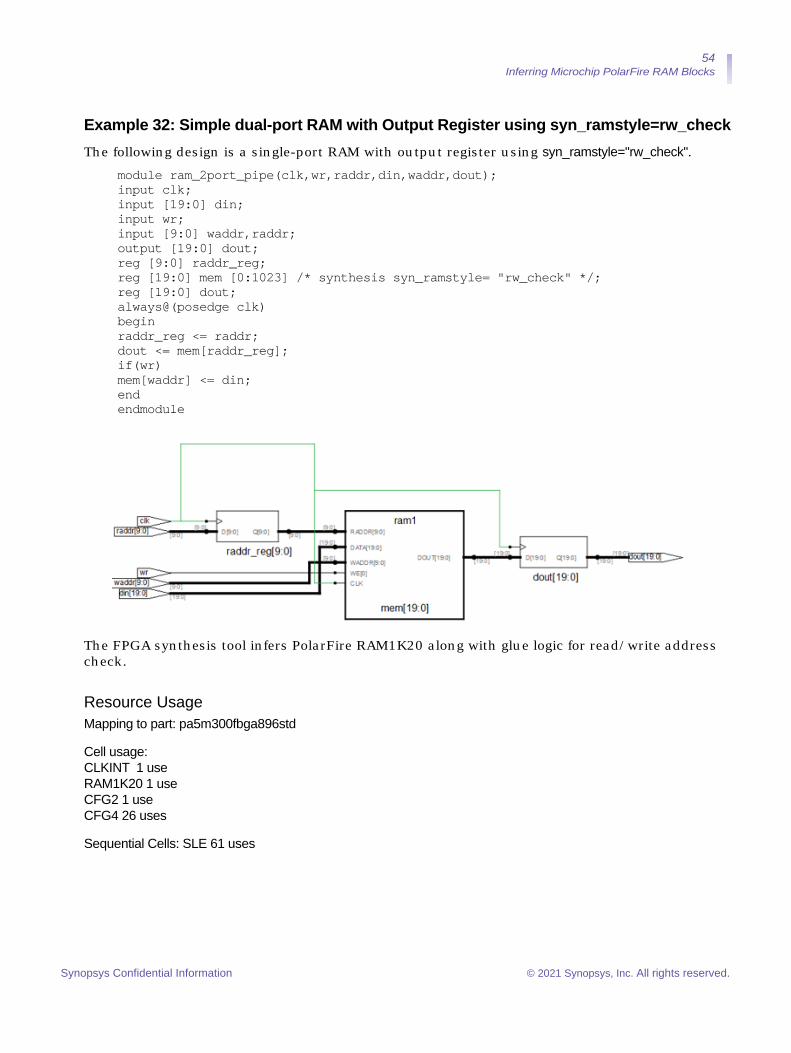
Example 32: Simple dual-port RAM with Output Register using syn_ramstyle=rw_checkThe following design is a single-port RAM with output register using syn_ramstyle="rw_check".
module ram_2port_pipe(clk,wr,raddr,din,waddr,dout); input clk; input [19:0] din; input wr; input [9:0] waddr,raddr; output [19:0] dout; reg [9:0] raddr_reg; reg [19:0] mem [0:1023] /* synthesis syn_ramstyle= "rw_check" */; reg [19:0] dout; always@(posedge clk) begin raddr_reg <= raddr; dout <= mem[raddr_reg]; if(wr) mem[waddr] <= din; end endmodule
The FPGA synthesis tool infers PolarFire RAM1K20 along with glue logic for read/write address check.
Resource UsageMapping to part: pa5m300fbga896std
Cell usage: CLKINT 1 use RAM1K20 1 use CFG2 1 use CFG4 26 uses
Sequential Cells: SLE 61 uses
Synopsys Confidential Information © 2021 Synopsys, Inc. All rights reserved.
55 Inferring Microchip PolarFire RAM Blocks
Example 33: Three-port RAM with Synchronous ReadThe following design is a Verilog example for three-port RAM with synchronous read.
module ram_infer15_rtl(clk,dinc,douta,doutb,wrc,addra,addrb,addrc); input clk; input [19:0] dinc; input wrc; input [5:0] addra, addrb, addrc; output [19:0] douta, doutb; reg [19:0] douta, doutb; reg [19:0] mem [0:63]; always@(posedge clk) begin if(wrc) mem[addrc] <= dinc; endalways@(posedge clk) begin douta <= mem[addra]; end always@(posedge clk) begin doutb <= mem[addrb]; end endmodule
RTL view
The tool infers PolarFire RAM64X12.
Synopsys Confidential Information © 2021 Synopsys, Inc. All rights reserved.

56 Inferring Microchip PolarFire RAM Blocks
Resource UsageMapping to part: pa5m300fbga896std
Cell usage: CLKINT 1 use RAM64x12 4 uses
Sequential Cells: SLE 0 uses
Example 34: Three-port RAM with Asynchronous ReadThe following design is a VHDL example for three-port RAM with asynchronous read.
library ieee; use ieee.std_logic_1164.all; use ieee.std_logic_unsigned.all; entity ram_singleport_noreg is port (d : in std_logic_vector(7 downto 0); addw : in std_logic_vector(6 downto 0); addr1 : in std_logic_vector(6 downto 0); addr2 : in std_logic_vector(6 downto 0); we : in std_logic; clk : in std_logic; q1 : out std_logic_vector(7 downto 0); q2 : out std_logic_vector(7 downto 0) ); end ram_singleport_noreg; architecture rtl of ram_singleport_noreg is type mem_type is array (127 downto 0) of std_logic_vector (7 downto 0); signal mem: mem_type; begin process (clk) begin if rising_edge(clk) then if (we = '1') then mem(conv_integer (addw)) <= d; end if; end if; end process; q1<= mem(conv_integer (addr1)); q2<= mem(conv_integer (addr2)); end rtl;
Synopsys Confidential Information © 2021 Synopsys, Inc. All rights reserved.

57 Inferring Microchip PolarFire RAM Blocks
The tool infers one RAM64X12.
Resource UsageMapping to part: pa5m300fbga896std Cell usage: RAM64x12 4 uses
Sequential Cells: SLE 0 uses
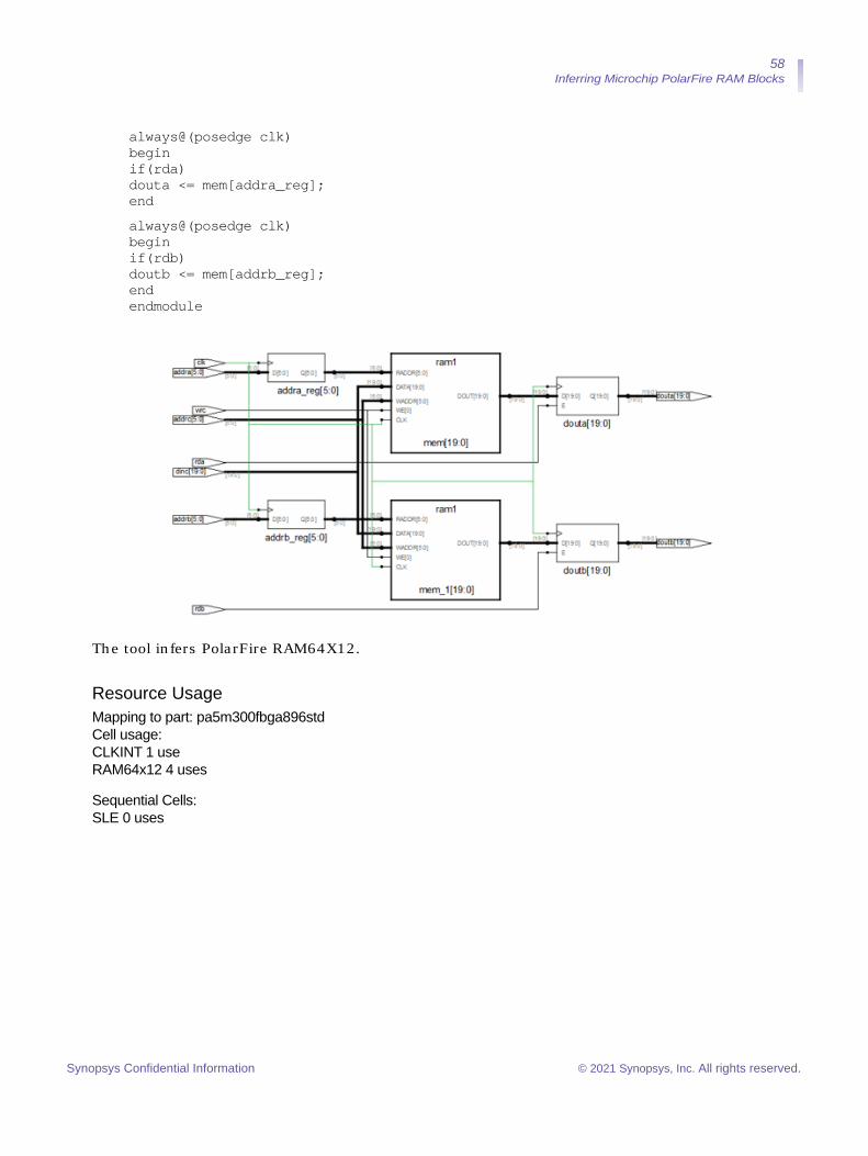
Example 35: Three-port RAM with read address and pipeline registerThe following design is an example for three-port RAM with read address and pipeline register.
module ram_infer(clk,dinc,douta,doutb,wrc,rda,rdb,addra,addrb,addrc); input clk; input [19:0] dinc; input wrc,rda,rdb; input [5:0] addra,addrb,addrc; output [19:0] douta,doutb; reg [19:0] douta,doutb; reg [5:0] addra_reg, addrb_reg;reg [19:0] mem [0:63]; always@(posedge clk) begin addra_reg <= addra; addrb_reg <= addrb;if(wrc) mem[addrc] <= dinc; end
Synopsys Confidential Information © 2021 Synopsys, Inc. All rights reserved.
58 Inferring Microchip PolarFire RAM Blocks
always@(posedge clk) begin if(rda) douta <= mem[addra_reg]; endalways@(posedge clk) begin if(rdb) doutb <= mem[addrb_reg]; end endmodule
The tool infers PolarFire RAM64X12.
Resource UsageMapping to part: pa5m300fbga896std Cell usage: CLKINT 1 use RAM64x12 4 uses
Sequential Cells: SLE 0 uses
Synopsys Confidential Information © 2021 Synopsys, Inc. All rights reserved.

59 Inferring Microchip PolarFire RAM Blocks
Example 36: Simple Dual-port RAM with enable on output registerThe following design is an example for simple dual-port RAM with enable on output register. When enable is deasserted, the RAM output is 0.
module ram_singleport_outreg_areset_en_rtl(clk,wr,addr,addw,din,dout,en);output [19:0] dout; input [19:0] din; input [9:0] addr, addw; input clk, wr, en; reg [19:0] dout; reg [19:0]mem[1023:0];always@(posedge clk) begin if(wr) mem[addw] <= din; endalways@(posedge clk) begin if(en) dout <= mem[addr]; else dout <= 0; endendmodule
The tool infers one RAM1K20 using A_BLK_EN pin for enable en. enable en pin is mapped using A_BLK_EN or B_BLK_EN pin on LSRAM only when one port of RAM1K20 is used for reading and another port for writing.
Synopsys Confidential Information © 2021 Synopsys, Inc. All rights reserved.

60 Inferring Microchip PolarFire RAM Blocks
Resource UsageMapping to part: pa5m300fbga896std Cell usage: CLKINT 1 use RAM1K20 1 use
Sequential Cells: SLE 0 uses
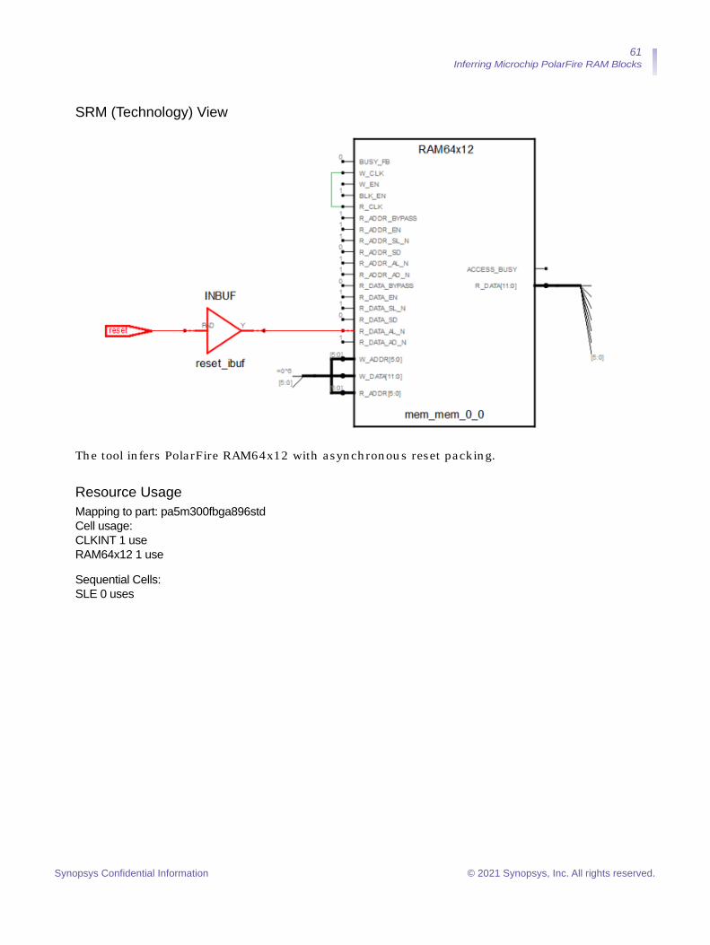
Example 37: Single-port RAM with Asynchronous Reset (URAM)The following design is a single-port RAM with asynchronous reset.
module ram_singleport_areset(clk,we,a,d,q1,reset); input [17:0] d; input [5:0] a; input clk, we,reset; output reg [5:0] q1; reg [17:0] mem [63:0];always @(posedge clk) begin if(we) mem[a] <= d; endalways @ (posedge clk or negedge reset) begin if (!reset) q1 <= 0; else q1 <= mem[a]; end endmodule
SRS (RTL) View
Synopsys Confidential Information © 2021 Synopsys, Inc. All rights reserved.
61 Inferring Microchip PolarFire RAM Blocks
SRM (Technology) View
The tool infers PolarFire RAM64x12 with asynchronous reset packing.
Resource UsageMapping to part: pa5m300fbga896std Cell usage: CLKINT 1 use RAM64x12 1 use
Sequential Cells: SLE 0 uses
Synopsys Confidential Information © 2021 Synopsys, Inc. All rights reserved.

62 Inferring Microchip PolarFire RAM Blocks
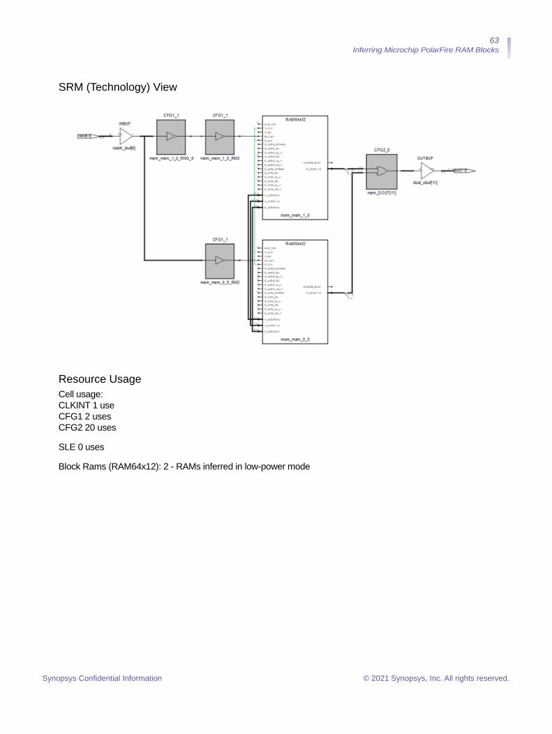
Example 38: Simple Dual-port URAM in Low Power ModeFor 128x12 RAM configuration, the tool fractures the data width and infers two URAM blocks.
When you set the global option low_power_ram_decomp 1 in the project file (*.prj), the tool fractures the address width to infer two URAMs. The tool connects the MSB bit of address to the BLK pin and OR gates at the output to select the output from the two RAM blocks.
RTLifdef synthesis module test (raddr, waddr, clk, we, din, dout); `else module test_RTL (raddr, waddr, clk, we, din, dout); `endifparameter ADDR_WIDTH = 7; parameter DATA_WIDTH = 12; parameter MEM_DEPTH = 128;input [ADDR_WIDTH-1:0]raddr; input [ADDR_WIDTH-1:0]waddr; input clk, we; output[DATA_WIDTH-1 : 0]dout; input [DATA_WIDTH-1 : 0]din;reg [DATA_WIDTH-1 : 0]dout; reg [DATA_WIDTH-1 : 0]mem[MEM_DEPTH-1 :0] ;always@(posedge clk) begin dout <= mem[raddr]; endalways@(posedge clk)
begin if(we) mem[waddr] <= din;
end endmodule
Project file option is set_option -low_power_ram_decomp 1.
SRS View (RTL)
Synopsys Confidential Information © 2021 Synopsys, Inc. All rights reserved.
63 Inferring Microchip PolarFire RAM Blocks
SRM (Technology) View
Resource UsageCell usage: CLKINT 1 use CFG1 2 uses CFG2 20 uses
SLE 0 uses
Block Rams (RAM64x12): 2 - RAMs inferred in low-power mode
Synopsys Confidential Information © 2021 Synopsys, Inc. All rights reserved.

64 Inferring Microchip PolarFire RAM Blocks
Example 39: Simple Dual-port LSRAM in Low Power ModeFor 2Kx20 RAM configuration, the tool fractures the data width and infers two LSRAM RAM blocks.
When you set the global option low_power_ram_decomp 1 in the project file (*.prj), the tool fractures the address width to infer two LSRAM blocks in 1Kx20 mode. The tool connects the MSB bit of address to the BLK pin and OR gates at the output, to select the output from two RAM blocks.
RTLmodule test (raddr, waddr, clk, we, din, dout); parameter ADDR_WIDTH = 11; parameter DATA_WIDTH = 20; parameter MEM_DEPTH = 2048; input [ADDR_WIDTH-1:0] raddr; input [ADDR_WIDTH-1:0] waddr; input clk, we; output[DATA_WIDTH-1 : 0]dout;input [DATA_WIDTH-1 : 0]din; reg [DATA_WIDTH-1 : 0]dout; reg [DATA_WIDTH-1 : 0]mem[MEM_DEPTH-1 :0] ; always@(posedge clk)
begin dout <= mem[raddr]; end always@(posedge clk)
begin if(we) mem[waddr] <= din;
end endmoduleProject File option is set_option -low_power_ram_decomp 1.
SRS View (RTL)
Synopsys Confidential Information © 2021 Synopsys, Inc. All rights reserved.
65 Inferring Microchip PolarFire RAM Blocks
SRM (Technology) View
Resource UsageCell usage:
CLKINT 1 use CFG1 2 uses CFG2 20 uses
SLE 0 uses Block Rams (RAM1K20): 2 - RAMs inferred in low-power mode
Synopsys Confidential Information © 2021 Synopsys, Inc. All rights reserved.
66 Inferring Microchip PolarFire RAM Blocks
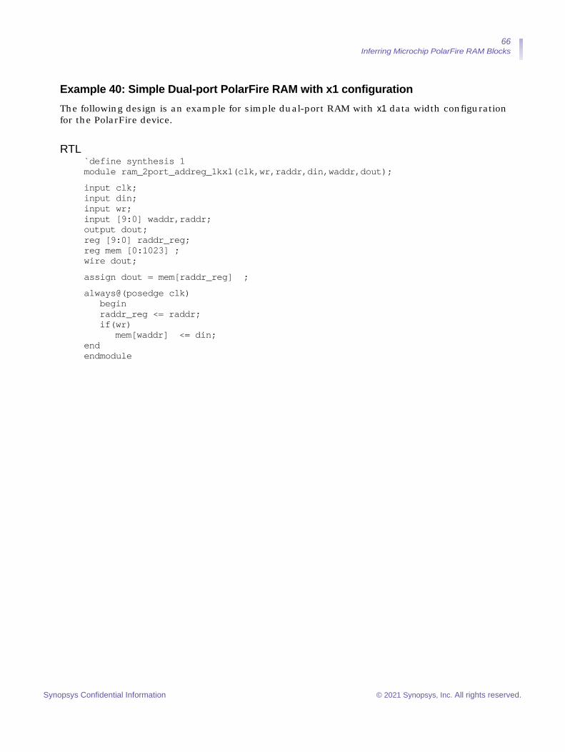
Example 40: Simple Dual-port PolarFire RAM with x1 configurationThe following design is an example for simple dual-port RAM with x1 data width configuration for the PolarFire device.
RTL`define synthesis 1 module ram_2port_addreg_1kx1(clk,wr,raddr,din,waddr,dout);input clk; input din; input wr; input [9:0] waddr,raddr; output dout; reg [9:0] raddr_reg; reg mem [0:1023] ; wire dout;assign dout = mem[raddr_reg] ;always@(posedge clk)
begin raddr_reg <= raddr; if(wr)
mem[waddr] <= din; end endmodule
Synopsys Confidential Information © 2021 Synopsys, Inc. All rights reserved.

67 Inferring Microchip PolarFire RAM Blocks
SRS View (RTL)
Resource Usage Cell usage: CLKINT 1 use
SLE 0 uses Block Rams (RAM1K20): 1
Synopsys Confidential Information © 2021 Synopsys, Inc. All rights reserved.

68 Inferring Microchip PolarFire RAM Blocks
Example 41: Single-port PolarFire RAM (VHDL)The following design is a VHDL example for PolarFire RAM with Read Enable to read from RAM. The output of RAM set to 0 when Read Enable is deasserted.
RTLlibrary ieee; use ieee.std_logic_1164.all; use ieee.std_logic_unsigned.all; entity ram_test is
port (d: in std_logic_vector(7 downto 0); a: in integer range 127 downto 0; we: in std_logic; re: in std_logic; clk: in std_logic; q: out std_logic_vector(7 downto 0) );
end ram_test;architecture rtl of ram_test is type mem_type is array (127 downto 0) of std_logic_vector (7 downto 0); signal mem: mem_type;attribute syn_ramstyle : string; attribute syn_ramstyle of mem : signal is "lsram";begin
process(clk) begin
if (clk'event and clk='1') then --q <= mem(a);
if (we='1') then mem(a) <= d; end if;
if (re='1') then q <= mem(a);
else q <= "00000000"; end if;
end if; end process;end rtl;
Synopsys Confidential Information © 2021 Synopsys, Inc. All rights reserved.

69 Inferring Microchip PolarFire RAM Blocks
SRS View (RTL)
SRM (Technology) View
Synopsys Confidential Information © 2021 Synopsys, Inc. All rights reserved.
70 Inferring Microchip PolarFire RAM Blocks
Resource UsageCell usage: CLKINT 1 use CFG1 1 use CFG2 8 uses
SLE 1 uses
Block Rams (RAM1K20): 1
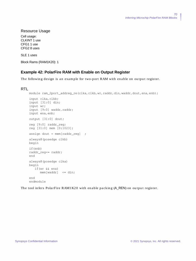
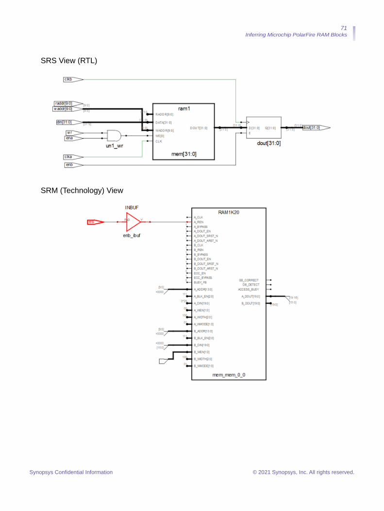
Example 42: PolarFire RAM with Enable on Output RegisterThe following design is an example for two-port RAM with enable on output register.
RTLmodule ram_2port_addreg_re(clka,clkb,wr,raddr,din,waddr,dout,ena,enb); input clka,clkb; input [31:0] din; input wr; input [9:0] waddr,raddr; input ena,enb; output [31:0] dout; reg [9:0] raddr_reg; reg [31:0] mem [0:1023]; assign dout = mem[raddr_reg] ; always@(posedge clkb) begin if(enb) raddr_reg<= raddr; end always@(posedge clka) begin
if(wr && ena) mem[waddr] <= din;
end endmodule
The tool infers PolarFire RAM1K20 with enable packing (A_REN) on output register.
Synopsys Confidential Information © 2021 Synopsys, Inc. All rights reserved.
71 Inferring Microchip PolarFire RAM Blocks
SRS View (RTL)
SRM (Technology) View
Synopsys Confidential Information © 2021 Synopsys, Inc. All rights reserved.
72 Inferring Microchip PolarFire RAM Blocks
Resource UsageCell usage: CLKINT 2 uses CFG2 1 use
SLE 0 uses
Block Rams (RAM1K20): 2
Example 43: Asymmetric RAM with write_width > read_width using Output Registermodule asymram_ww_gt_rw_outreg(din,dout,addra,addrb,clk,wen);parameter din_width = 20; parameter dout_width = 10; parameter addra_width = 10; parameter addrb_width = 11;localparam ratio= 2; localparam max_depth=2048; localparam min_width=10;input clk,wen; input [din_width-1 : 0] din; input [addra_width-1 : 0] addra; input [addrb_width-1 : 0] addrb; output reg [dout_width-1 : 0] dout;reg [min_width-1:0] mem_ram[max_depth-1:0]; always @(posedge clk) begin
if(wen) begin
mem_ram[{addra,1'b0}]<=din[min_width*0+:min_width]; mem_ram[{addra,1'b1}]<=din[min_width*1+:min_width];
end end always @(posedge clk) begin
dout <=mem_ram[addrb]; end endmodule
Synopsys Confidential Information © 2021 Synopsys, Inc. All rights reserved.

73 Inferring Microchip PolarFire RAM Blocks
The tool infers PolarFire RAM1K20.
Resource Usage Report Mapping to part: mpf300tfcg1152std Cell usage: CLKINT 1 use Sequential Cells: SLE 0 uses DSP Blocks: 0 of 924 (0%) I/O ports: 53 I/O primitives: 53 INBUF 43 uses OUTBUF 10 uses Global Clock Buffers: 1 RAM/ROM usage summary Total Block RAMs (RAM1K20) : 1 of 952 (0%) Total LUTs: 0
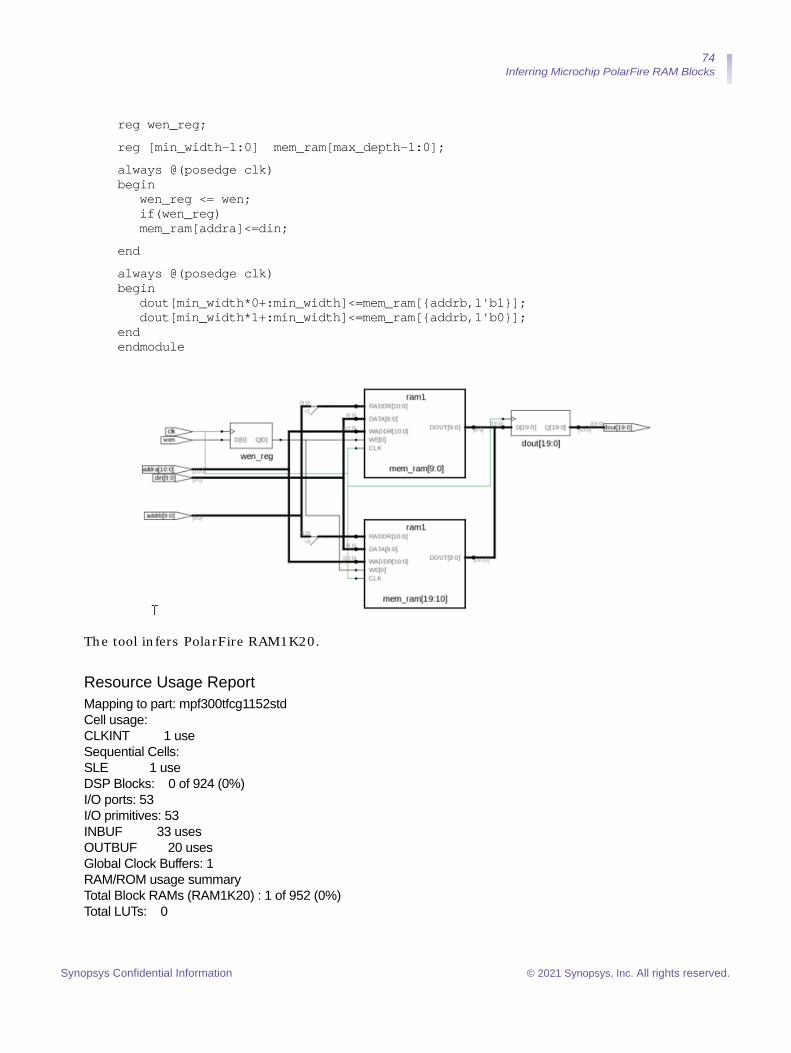
Example 44: Asymmetric RAM with write_width < read_width using Output Registermodule asymram_rw_gt_rw_outreg(din,dout,addra,addrb,clk,wen);parameter din_width = 10; parameter dout_width = 20; parameter addra_width = 11; parameter addrb_width = 10;localparam ratio= 2; localparam max_depth=2048; localparam min_width=10;input clk,wen; input [din_width-1 : 0] din; input [addra_width-1 : 0] addra; input [addrb_width-1 : 0] addrb; output reg [dout_width-1 : 0] dout;
Synopsys Confidential Information © 2021 Synopsys, Inc. All rights reserved.
74 Inferring Microchip PolarFire RAM Blocks
reg wen_reg;reg [min_width-1:0] mem_ram[max_depth-1:0];always @(posedge clk) begin
wen_reg <= wen; if(wen_reg) mem_ram[addra]<=din;
end always @(posedge clk) begin
dout[min_width*0+:min_width]<=mem_ram[{addrb,1'b1}]; dout[min_width*1+:min_width]<=mem_ram[{addrb,1'b0}];
end endmodule
The tool infers PolarFire RAM1K20.
Resource Usage ReportMapping to part: mpf300tfcg1152std Cell usage: CLKINT 1 use Sequential Cells: SLE 1 use DSP Blocks: 0 of 924 (0%) I/O ports: 53 I/O primitives: 53 INBUF 33 uses OUTBUF 20 uses Global Clock Buffers: 1 RAM/ROM usage summary Total Block RAMs (RAM1K20) : 1 of 952 (0%) Total LUTs: 0
Synopsys Confidential Information © 2021 Synopsys, Inc. All rights reserved.
75 Inferring Microchip PolarFire RAM Blocks
Example 45: Asymmetric RAM with write_width > read_width; No change modemodule asymram_ren_nochange(din,dout,addra,addrb,clk,wen,ren);parameter din_width = 16; parameter dout_width = 2; parameter addra_width = 10; parameter addrb_width = 13;localparam ratio= 8; localparam max_depth=8192; localparam min_width=2;input clk,wen,ren; input [din_width-1 : 0] din; input [addra_width-1 : 0] addra; input [addrb_width-1 : 0] addrb; output reg [dout_width-1 : 0] dout;reg [min_width-1:0] mem_ram[max_depth-1:0]; always @(posedge clk)
begin if(wen) begin
mem_ram[{addra,3'd0}]<=din[min_width*0+:min_width]; mem_ram[{addra,3'd1}]<=din[min_width*1+:min_width]; mem_ram[{addra,3'd2}]<=din[min_width*2+:min_width]; mem_ram[{addra,3'd3}]<=din[min_width*3+:min_width]; mem_ram[{addra,3'd4}]<=din[min_width*4+:min_width]; mem_ram[{addra,3'd5}]<=din[min_width*5+:min_width]; mem_ram[{addra,3'd6}]<=din[min_width*6+:min_width]; mem_ram[{addra,3'd7}]<=din[min_width*7+:min_width];
end endalways @(posedge clk) begin
if(!wen && ren) begin
dout <= mem_ram[addrb]; end
endendmodule
Synopsys Confidential Information © 2021 Synopsys, Inc. All rights reserved.

76 Inferring Microchip PolarFire RAM Blocks
The tool infers PolarFire RAM1K20.
Resource Usage ReportMapping to part: mpf300tfcg1152std Cell usage: CLKINT 1 use CFG2 1 use Sequential Cells: SLE 0 uses DSP Blocks: 0 of 924 (0%) I/O ports: 44 I/O primitives: 44 INBUF 42 uses OUTBUF 2 uses Global Clock Buffers: 1
Synopsys Confidential Information © 2021 Synopsys, Inc. All rights reserved.
77 Inferring Microchip PolarFire RAM Blocks
RAM/ROM usage summary Total Block RAMs (RAM1K20) : 1 of 952 (0%) Total LUTs: 1
Example 46: Asymmetric RAM with write_width < read_width; No change modemodule asymram_ren_nochange(din,dout,addra,addrb,clk,wen,ren);parameter din_width = 2; parameter dout_width = 16; parameter addra_width = 13; parameter addrb_width = 10;localparam ratio= 8; localparam max_depth=8192; localparam min_width=2;input clk,wen,ren; input [din_width-1 : 0] din; input [addra_width-1 : 0] addra; input [addrb_width-1 : 0] addrb; output reg [dout_width-1 : 0] dout; reg [$clog2(ratio):0] i; wire [dout_width-1 : 0] dout1; reg [min_width-1:0] mem_ram[max_depth-1:0]; always @(posedge clk) begin
if(wen) begin
mem_ram[addra]<=din; end else if(ren) begin
dout[min_width*0+:min_width]<=mem_ram[{addrb,3'd0}]; dout[min_width*1+:min_width]<=mem_ram[{addrb,3'd1}]; dout[min_width*2+:min_width]<=mem_ram[{addrb,3'd2}]; dout[min_width*3+:min_width]<=mem_ram[{addrb,3'd3}]; dout[min_width*4+:min_width]<=mem_ram[{addrb,3'd4}]; dout[min_width*5+:min_width]<=mem_ram[{addrb,3'd5}]; dout[min_width*6+:min_width]<=mem_ram[{addrb,3'd6}]; dout[min_width*7+:min_width]<=mem_ram[{addrb,3'd7}];
end endendmodule
Synopsys Confidential Information © 2021 Synopsys, Inc. All rights reserved.
78 Inferring Microchip PolarFire RAM Blocks
The tool infers PolarFire RAM1K20.
Resource Usage ReportMapping to part: mpf300tfcg1152std Cell usage: CLKINT 1 use CFG2 1 use Sequential Cells: SLE 0 uses DSP Blocks: 0 of 924 (0%) I/O ports: 44 I/O primitives: 44 INBUF 28 uses OUTBUF 16 uses Global Clock Buffers: 1
Synopsys Confidential Information © 2021 Synopsys, Inc. All rights reserved.

79 Inferring Microchip PolarFire RAM Blocks
RAM/ROM usage summary Total Block RAMs (RAM1K20) : 1 of 952 (0%) Total LUTs: 1
Example 47: Asymmetric RAM with write_width > read_width; write-first modemodule asymram_writefirst(din,dout,addra,addrb,clk,wen);parameter din_width = 4; parameter dout_width = 2; parameter addra_width = 12; parameter addrb_width = 13;localparam ratio= 2; localparam max_depth=8192; localparam min_width=2;input clk,wen; input [din_width-1 : 0] din; input [addra_width-1 : 0] addra; input [addrb_width-1 : 0] addrb; output reg [dout_width-1 : 0] dout;reg [addrb_width-1 : 0] addrb_reg;reg [min_width-1:0] mem_ram[max_depth-1:0]; always @(posedge clk) begin
if(wen) begin
mem_ram[{addra,1'b0}]<=din[min_width*0+:min_width]; mem_ram[{addra,1'b1}]<=din[min_width*1+:min_width];
end end always @(posedge clk) begin
addrb_reg <= addrb; dout <=mem_ram[addrb_reg];
end endmodule
Synopsys Confidential Information © 2021 Synopsys, Inc. All rights reserved.

80 Inferring Microchip PolarFire RAM Blocks
The tool infers PolarFire RAM1K20.
Resource Usage Report Mapping to part: mpf300tfcg1152std Cell usage: CLKINT 1 use Sequential Cells: SLE 0 uses DSP Blocks: 0 of 924 (0%) I/O ports: 33 I/O primitives: 33 INBUF 31 uses OUTBUF 2 uses Global Clock Buffers: 1 RAM/ROM usage summary Total Block RAMs (RAM1K20) : 1 of 952 (0%) Total LUTs: 0
Example 48: Asymmetric RAM with write_width < read_width with Output Register; Write-first mode
module asymram_writefirst(din,dout,addra,addrb,clk,wen);parameter din_width = 2; parameter dout_width = 4; parameter addra_width = 13; parameter addrb_width = 12;localparam ratio= 2; localparam max_depth=8196; localparam min_width=2;input clk,wen; input [din_width-1 : 0] din; input [addra_width-1 : 0] addra; input [addrb_width-1 : 0] addrb; output reg [dout_width-1 : 0] dout;
Synopsys Confidential Information © 2021 Synopsys, Inc. All rights reserved.
81 Inferring Microchip PolarFire RAM Blocks
reg [addrb_width-1 : 0] addrb_reg;reg [min_width-1:0] mem_ram[max_depth-1:0];always @(posedge clk) begin addrb_reg <= addrb;
if(wen) mem_ram[addra]<=din;
end always @(posedge clk) begin
dout[min_width*0+:min_width]<=mem_ram[{addrb_reg,1'b0}]; dout[min_width*1+:min_width]<=mem_ram[{addrb_reg,1'b1}];
end endmodule
The tool infers PolarFire RAM1K20.
Resource Usage Report Mapping to part: mpf300tfcg1152std Cell usage: CLKINT 1 use Sequential Cells: SLE 0 uses DSP Blocks: 0 of 924 (0%) I/O ports: 33 I/O primitives: 33 INBUF 29 uses OUTBUF 4 uses Global Clock Buffers: 1
Synopsys Confidential Information © 2021 Synopsys, Inc. All rights reserved.

82 Inferring Microchip PolarFire RAM Blocks
RAM/ROM usage summary Total Block RAMs (RAM1K20) : 1 of 952 (0%) Total LUTs: 0
Example 49: Asymmetric RAM with write_width > read_width; Read-first modemodule asymram_readfirst_norwcheck(din,dout,addra,addrb,clk,wen);parameter din_width = 4; parameter dout_width = 1; parameter addra_width = 12; parameter addrb_width = 14;localparam ratio= 4; localparam max_depth=16384; localparam min_width=1;input clk,wen; input [din_width-1 : 0] din; input [addra_width-1 : 0] addra; input [addrb_width-1 : 0] addrb; output reg [dout_width-1 : 0] dout;reg [min_width-1:0] mem_ram[max_depth-1:0] /*synthesis syn_ramstyle = "no_rw_check" */; always @(posedge clk)
begin if(wen) begin
mem_ram[{addra,2'd0}]<=din[min_width*0+:min_width]; mem_ram[{addra,2'd1}]<=din[min_width*1+:min_width]; mem_ram[{addra,2'd2}]<=din[min_width*2+:min_width]; mem_ram[{addra,2'd3}]<=din[min_width*3+:min_width];
end end
always @(posedge clk) begin
dout <=mem_ram[addrb]; end endmodule
Synopsys Confidential Information © 2021 Synopsys, Inc. All rights reserved.

83 Inferring Microchip PolarFire RAM Blocks
The tool infers PolarFire RAM1K20.
Resource Usage Report Mapping to part: mpf300tfcg1152std Cell usage: CLKINT 1 use Sequential Cells: SLE 0 uses DSP Blocks: 0 of 924 (0%) I/O ports: 33 I/O primitives: 33 INBUF 32 uses OUTBUF 1 use Global Clock Buffers: 1 RAM/ROM usage summary Total Block RAMs (RAM1K20) : 1 of 952 (0%) Total LUTs: 0
Synopsys Confidential Information © 2021 Synopsys, Inc. All rights reserved.
84 Inferring Microchip PolarFire RAM Blocks
Example 50: Asymmetric RAM with write_width < read_width with Output Registermodule asymram_readfirst_norwcheck(din,dout,addra,addrb,clk,wen);parameter din_width = 1; parameter dout_width = 4; parameter addra_width = 14; parameter addrb_width = 12;localparam ratio= 4; localparam max_depth=16384; localparam min_width=1;input clk,wen; input [din_width-1 : 0] din; input [addra_width-1 : 0] addra; input [addrb_width-1 : 0] addrb; output reg [dout_width-1 : 0] dout; reg [$clog2(ratio):0] i; reg [min_width-1:0] mem_ram[max_depth-1:0] /*synthesis syn_ramstyle="no_rw_check" */;always @(posedge clk) begin
if(wen) mem_ram[addra]<=din;
end always @(posedge clk) begin
dout[min_width*0+:min_width]<=mem_ram[{addrb,2'd0}]; dout[min_width*1+:min_width]<=mem_ram[{addrb,2'd1}]; dout[min_width*2+:min_width]<=mem_ram[{addrb,2'd2}]; dout[min_width*3+:min_width]<=mem_ram[{addrb,2'd3}];
endendmodule
Synopsys Confidential Information © 2021 Synopsys, Inc. All rights reserved.
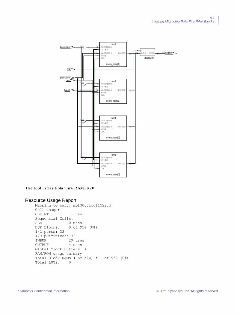
85 Inferring Microchip PolarFire RAM Blocks
The tool infers PolarFire RAM1K20.
Resource Usage Report Mapping to part: mpf300tfcg1152std Cell usage: CLKINT 1 use Sequential Cells: SLE 0 uses DSP Blocks: 0 of 924 (0%) I/O ports: 33 I/O primitives: 33 INBUF 29 uses OUTBUF 4 uses Global Clock Buffers: 1 RAM/ROM usage summary Total Block RAMs (RAM1K20) : 1 of 952 (0%) Total LUTs: 0
Synopsys Confidential Information © 2021 Synopsys, Inc. All rights reserved.

86 Inferring Microchip PolarFire RAM Blocks
Example 51: Asymmetric RAM with write_width>read_width with Output Register having Active High Asynchronous Reset
module asymram_ren_arst(din,dout,addra,addrb,clk,wen,ren,arst);parameter din_width = 16; parameter dout_width = 2; parameter addra_width = 10; parameter addrb_width = 13;localparam ratio= 8; localparam max_depth=8192; localparam min_width=2;input clk,wen,ren,arst; input [din_width-1 : 0] din; input [addra_width-1 : 0] addra; input [addrb_width-1 : 0] addrb; output reg [dout_width-1 : 0] dout; reg [$clog2(ratio):0] i; reg [min_width-1:0] mem_ram[max_depth-1:0];
always @(posedge clk) begin
if(wen) begin
mem_ram[{addra,3'd0}]<=din[min_width*0+:min_width]; mem_ram[{addra,3'd1}]<=din[min_width*1+:min_width]; mem_ram[{addra,3'd2}]<=din[min_width*2+:min_width]; mem_ram[{addra,3'd3}]<=din[min_width*3+:min_width]; mem_ram[{addra,3'd4}]<=din[min_width*4+:min_width];
mem_ram[{addra,3'd5}]<=din[min_width*5+:min_width]; mem_ram[{addra,3'd6}]<=din[min_width*6+:min_width]; mem_ram[{addra,3'd7}]<=din[min_width*7+:min_width];
end endalways @(posedge clk or posedge arst) begin
if(arst) dout <= 0;
else if (ren) dout <=mem_ram[addrb]; end endmodule
Synopsys Confidential Information © 2021 Synopsys, Inc. All rights reserved.
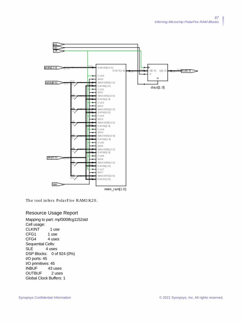
87 Inferring Microchip PolarFire RAM Blocks
The tool infers PolarFire RAM1K20.
Resource Usage Report Mapping to part: mpf300tfcg1152std Cell usage: CLKINT 1 use CFG1 1 use CFG4 4 uses Sequential Cells: SLE 4 uses DSP Blocks: 0 of 924 (0%) I/O ports: 45 I/O primitives: 45 INBUF 43 uses OUTBUF 2 uses Global Clock Buffers: 1
Synopsys Confidential Information © 2021 Synopsys, Inc. All rights reserved.

88 Inferring Microchip PolarFire RAM Blocks
RAM/ROM usage summary Total Block RAMs (RAM1K20) : 1 of 952 (0%) Total LUTs: 5
Example 52: Asymmetric RAM with write_width<read_width with Read address Register having Active High Asynchronous Reset
module asymram_arst(din,dout,addra,addrb,clk,wen,arst);parameter din_width = 5; parameter dout_width = 20; parameter addra_width = 12; parameter addrb_width = 10;localparam ratio= 4; localparam max_depth=4096; localparam min_width=5;input clk,wen,arst; input [din_width-1 : 0] din; input [addra_width-1 : 0] addra; input [addrb_width-1 : 0] addrb; output reg [dout_width-1 : 0] dout; reg [$clog2(ratio):0] i; reg [addrb_width-1 : 0] addrb_reg;reg [min_width-1:0] mem_ram[max_depth-1:0];always @(posedge clk) begin
if(wen) mem_ram[addra]<=din;
end always @(posedge clk or posedge arst) begin
if(arst) addrb_reg <= 0;
else addrb_reg <= addrb;
end always @(posedge clk) begin
dout[min_width*0+:min_width]<=mem_ram[{addrb_reg,2'd0}]; dout[min_width*1+:min_width]<=mem_ram[{addrb_reg,2'd1}]; dout[min_width*2+:min_width]<=mem_ram[{addrb_reg,2'd2}]; dout[min_width*3+:min_width]<=mem_ram[{addrb_reg,2'd3}];
end endmodule
Synopsys Confidential Information © 2021 Synopsys, Inc. All rights reserved.
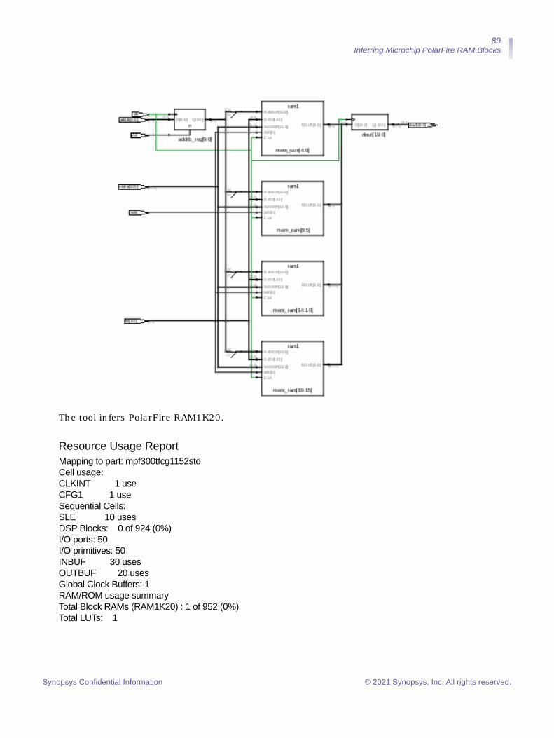
89 Inferring Microchip PolarFire RAM Blocks
The tool infers PolarFire RAM1K20.
Resource Usage Report Mapping to part: mpf300tfcg1152std Cell usage: CLKINT 1 use CFG1 1 use Sequential Cells: SLE 10 uses DSP Blocks: 0 of 924 (0%) I/O ports: 50 I/O primitives: 50 INBUF 30 uses OUTBUF 20 uses Global Clock Buffers: 1 RAM/ROM usage summary Total Block RAMs (RAM1K20) : 1 of 952 (0%) Total LUTs: 1
Synopsys Confidential Information © 2021 Synopsys, Inc. All rights reserved.
90 Inferring Microchip PolarFire RAM Blocks
Example 53: Asymmetric RAM with write_width > read_width with Pipeline Register & Output Register having Enable
module asymram_outpipe_en(din,dout,addra,addrb,clk,wen,en);parameter din_width = 8; parameter dout_width = 1; parameter addra_width = 11; parameter addrb_width = 14;localparam ratio= 8; localparam max_depth=16384; localparam min_width=1;input clk,wen,en; input [din_width-1 : 0] din; input [addra_width-1 : 0] addra; input [addrb_width-1 : 0] addrb; output reg [dout_width-1 : 0] dout;reg [dout_width-1 : 0] dout1;reg [min_width-1:0] mem_ram[max_depth-1:0]; always @(posedge clk)
begin if(wen) begin
mem_ram[{addra,3'd0}]<=din[min_width*0+:min_width]; mem_ram[{addra,3'd1}]<=din[min_width*1+:min_width]; mem_ram[{addra,3'd2}]<=din[min_width*2+:min_width]; mem_ram[{addra,3'd3}]<=din[min_width*3+:min_width]; mem_ram[{addra,3'd4}]<=din[min_width*4+:min_width]; mem_ram[{addra,3'd5}]<=din[min_width*5+:min_width]; mem_ram[{addra,3'd6}]<=din[min_width*6+:min_width]; mem_ram[{addra,3'd7}]<=din[min_width*7+:min_width];
end end
always @(posedge clk) begin
dout1 <=mem_ram[addrb]; end always @(posedge clk) begin
if(en) dout <=dout1;
endendmodule
Synopsys Confidential Information © 2021 Synopsys, Inc. All rights reserved.

91 Inferring Microchip PolarFire RAM Blocks
The tool infers PolarFire RAM1K20.
Resource Usage Report for asymram_outpipe_en Mapping to part: mpf300tfcg1152std Cell usage: CLKINT 1 use Sequential Cells: SLE 0 uses DSP Blocks: 0 of 924 (0%) I/O ports: 37 I/O primitives: 37 INBUF 36 uses OUTBUF 1 use Global Clock Buffers: 1 RAM/ROM usage summary Total Block RAMs (RAM1K20) : 1 of 952 (0%) Total LUTs: 0
Synopsys Confidential Information © 2021 Synopsys, Inc. All rights reserved.
92 Inferring Microchip PolarFire RAM Blocks
Example 54: Asymmetric RAM with write_width<read_width with Pipeline Register & Output Register having Enable
module asymram_outpipe_en(din,dout,addra,addrb,clk,wen,en);parameter din_width = 1; parameter dout_width = 8; parameter addra_width = 14; parameter addrb_width = 11;localparam ratio= 8; localparam max_depth=16384; localparam min_width=1;input clk,wen,en; input [din_width-1 : 0] din; input [addra_width-1 : 0] addra; input [addrb_width-1 : 0] addrb; output reg [dout_width-1 : 0] dout; reg [$clog2(ratio):0] i; reg [dout_width-1 : 0] dout1;reg [min_width-1:0] mem_ram[max_depth-1:0];always @(posedge clk) begin
if(wen) mem_ram[addra]<=din;
end always @(posedge clk) begin
dout1[min_width*0+:min_width]<=mem_ram[{addrb,3'd0}]; dout1[min_width*1+:min_width]<=mem_ram[{addrb,3'd1}]; dout1[min_width*2+:min_width]<=mem_ram[{addrb,3'd2}]; dout1[min_width*3+:min_width]<=mem_ram[{addrb,3'd3}]; dout1[min_width*4+:min_width]<=mem_ram[{addrb,3'd4}]; dout1[min_width*5+:min_width]<=mem_ram[{addrb,3'd5}]; dout1[min_width*6+:min_width]<=mem_ram[{addrb,3'd6}]; dout1[min_width*7+:min_width]<=mem_ram[{addrb,3'd7}];
endalways @(posedge clk) begin
if (en) dout <= dout1;
end endmodule
Synopsys Confidential Information © 2021 Synopsys, Inc. All rights reserved.
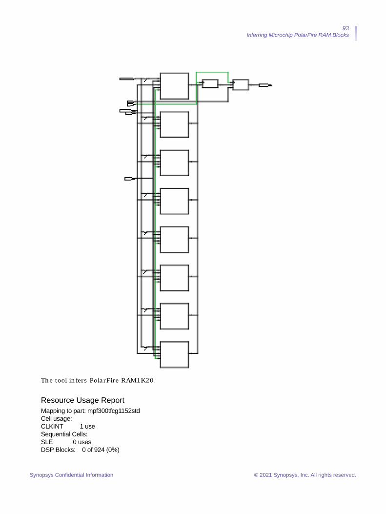
93 Inferring Microchip PolarFire RAM Blocks
The tool infers PolarFire RAM1K20.
Resource Usage Report Mapping to part: mpf300tfcg1152std Cell usage: CLKINT 1 use Sequential Cells: SLE 0 uses DSP Blocks: 0 of 924 (0%)
Synopsys Confidential Information © 2021 Synopsys, Inc. All rights reserved.
94 Inferring Microchip PolarFire RAM Blocks
I/O ports: 37 I/O primitives: 37 INBUF 29 uses OUTBUF 8 uses Global Clock Buffers: 1 RAM/ROM usage summary Total Block RAMs (RAM1K20) : 1 of 952 (0%) Total LUTs: 0
Example 55: Asymmetric RAM with write_width > read_width with Pipeline Register and Output Register having Active high Synchronous Reset
module asymram_ren_srst(din,dout,addra,addrb,clk,wen,ren,srst);parameter din_width = 32; parameter dout_width = 2; parameter addra_width = 9; parameter addrb_width = 13;localparam ratio= 16; localparam max_depth=8196; localparam min_width=2;input clk,wen,ren,srst; input [din_width-1 : 0] din; input [addra_width-1 : 0] addra; input [addrb_width-1 : 0] addrb; output reg [dout_width-1 : 0] dout;reg [min_width-1:0] mem_ram[max_depth-1:0]; always @(posedge clk)
begin if(wen) begin
mem_ram[{addra,4'd0}]<=din[min_width*0+:min_width]; mem_ram[{addra,4'd1}]<=din[min_width*1+:min_width]; mem_ram[{addra,4'd2}]<=din[min_width*2+:min_width]; mem_ram[{addra,4'd3}]<=din[min_width*3+:min_width]; mem_ram[{addra,4'd4}]<=din[min_width*4+:min_width]; mem_ram[{addra,4'd5}]<=din[min_width*5+:min_width]; mem_ram[{addra,4'd6}]<=din[min_width*6+:min_width]; mem_ram[{addra,4'd7}]<=din[min_width*7+:min_width]; mem_ram[{addra,4'd8}]<=din[min_width*8+:min_width]; mem_ram[{addra,4'd9}]<=din[min_width*9+:min_width]; mem_ram[{addra,4'd10}]<=din[min_width*10+:min_width]; mem_ram[{addra,4'd11}]<=din[min_width*11+:min_width]; mem_ram[{addra,4'd12}]<=din[min_width*12+:min_width]; mem_ram[{addra,4'd13}]<=din[min_width*13+:min_width]; mem_ram[{addra,4'd14}]<=din[min_width*14+:min_width]; mem_ram[{addra,4'd15}]<=din[min_width*15+:min_width];
end end always @(posedge clk) begin
if(srst)
Synopsys Confidential Information © 2021 Synopsys, Inc. All rights reserved.

95 Inferring Microchip PolarFire RAM Blocks
begin dout <= 0;
end else if(ren)
dout <=mem_ram[addrb]; end endmodule
The tool infers PolarFire RAM1K20.
Synopsys Confidential Information © 2021 Synopsys, Inc. All rights reserved.
96 Inferring Microchip PolarFire RAM Blocks
Resource Usage Report Mapping to part: mpf300tfcg1152std Cell usage: CLKINT 1 use CFG1 1 use CFG2 1 use CFG3 2 uses Sequential Cells: SLE 3 uses DSP Blocks: 0 of 924 (0%) I/O ports: 60 I/O primitives: 60 INBUF 58 uses OUTBUF 2 uses Global Clock Buffers: 1 RAM/ROM usage summary Total Block RAMs (RAM1K20) : 1 of 952 (0%) Total LUTs: 4
Example 56: Asymmetric RAM with write_width < read_width with Pipeline Register & Output Register having Active High Synchronous Reset
module asymram_ren_srst(din,dout,addra,addrb,clk,wen,ren,srst);parameter din_width = 2; parameter dout_width = 32; parameter addra_width = 13; parameter addrb_width = 9;localparam ratio= 16; localparam max_depth=8192; localparam min_width=2;input clk,wen,ren,srst; input [din_width-1 : 0] din; input [addra_width-1 : 0] addra; input [addrb_width-1 : 0] addrb; output reg [dout_width-1 : 0] dout;reg [dout_width-1 : 0] dout1; reg [min_width-1:0] mem_ram[max_depth-1:0];
reg [$clog2(ratio):0] i; always @(posedge clk) begin
if(wen) mem_ram[addra]<=din;
endalways @(posedge clk) begin
if(ren) begin
dout1[min_width*0+:min_width]<=mem_ram[{addrb,4'd0}]; dout1[min_width*1+:min_width]<=mem_ram[{addrb,4'd1}]; dout1[min_width*2+:min_width]<=mem_ram[{addrb,4'd2}];
Synopsys Confidential Information © 2021 Synopsys, Inc. All rights reserved.
97 Inferring Microchip PolarFire RAM Blocks
dout1[min_width*3+:min_width]<=mem_ram[{addrb,4'd3}]; dout1[min_width*4+:min_width]<=mem_ram[{addrb,4'd4}]; dout1[min_width*5+:min_width]<=mem_ram[{addrb,4'd5}]; dout1[min_width*6+:min_width]<=mem_ram[{addrb,4'd6}]; dout1[min_width*7+:min_width]<=mem_ram[{addrb,4'd7}]; dout1[min_width*8+:min_width]<=mem_ram[{addrb,4'd8}]; dout1[min_width*9+:min_width]<=mem_ram[{addrb,4'd9}]; dout1[min_width*10+:min_width]<=mem_ram[{addrb,4'd10}]; dout1[min_width*11+:min_width]<=mem_ram[{addrb,4'd11}]; dout1[min_width*12+:min_width]<=mem_ram[{addrb,4'd12}]; dout1[min_width*13+:min_width]<=mem_ram[{addrb,4'd13}]; dout1[min_width*14+:min_width]<=mem_ram[{addrb,4'd14}]; dout1[min_width*15+:min_width]<=mem_ram[{addrb,4'd15}];
end endalways @(posedge clk) begin
if(srst) begin
dout <= 0; end else begin
dout <= dout1; end
endendmodule
Synopsys Confidential Information © 2021 Synopsys, Inc. All rights reserved.
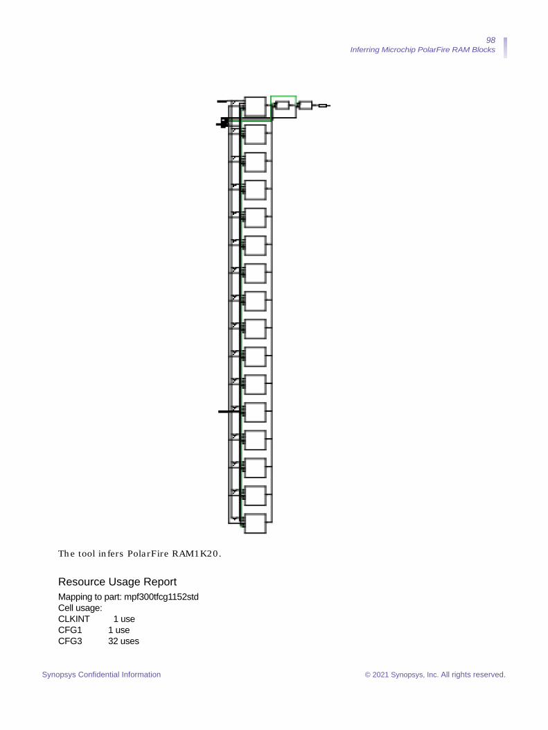
98 Inferring Microchip PolarFire RAM Blocks
The tool infers PolarFire RAM1K20.
Resource Usage Report Mapping to part: mpf300tfcg1152std Cell usage: CLKINT 1 use CFG1 1 use CFG3 32 uses
Synopsys Confidential Information © 2021 Synopsys, Inc. All rights reserved.

99 Inferring Microchip PolarFire RAM Blocks
Sequential Cells: SLE 65 uses DSP Blocks: 0 of 924 (0%) I/O ports: 60 I/O primitives: 60 INBUF 28 uses OUTBUF 32 uses Global Clock Buffers: 1 RAM/ROM usage summary Total Block RAMs (RAM1K20) : 1 of 952 (0%) Total LUTs: 33
Example 57: Asymmetric RAM with write_width > read_width using Pipeline Register & Output Register with Synchronous Reset
module asymram_outpipe_srst(din,dout,addra,addrb,clk,wen,srst);parameter din_width = 8; parameter dout_width = 2; parameter addra_width = 10; parameter addrb_width = 13;localparam ratio= 4; localparam max_depth=8192; localparam min_width=2;input clk,wen,srst; input [din_width-1 : 0] din; input [addra_width-1 : 0] addra; input [addrb_width-1 : 0] addrb; output reg [dout_width-1 : 0] dout;reg [dout_width-1 : 0] dout1;reg [min_width-1:0] mem_ram[max_depth-1:0]; always @(posedge clk) begin
if(wen) begin
mem_ram[{addra,2'd0}]<=din[min_width*0+:min_width]; mem_ram[{addra,2'd1}]<=din[min_width*1+:min_width]; mem_ram[{addra,2'd2}]<=din[min_width*2+:min_width]; mem_ram[{addra,2'd3}]<=din[min_width*3+:min_width];
end endalways @(posedge clk) begin
dout1 <=mem_ram[addrb]; end always @(posedge clk)
Synopsys Confidential Information © 2021 Synopsys, Inc. All rights reserved.
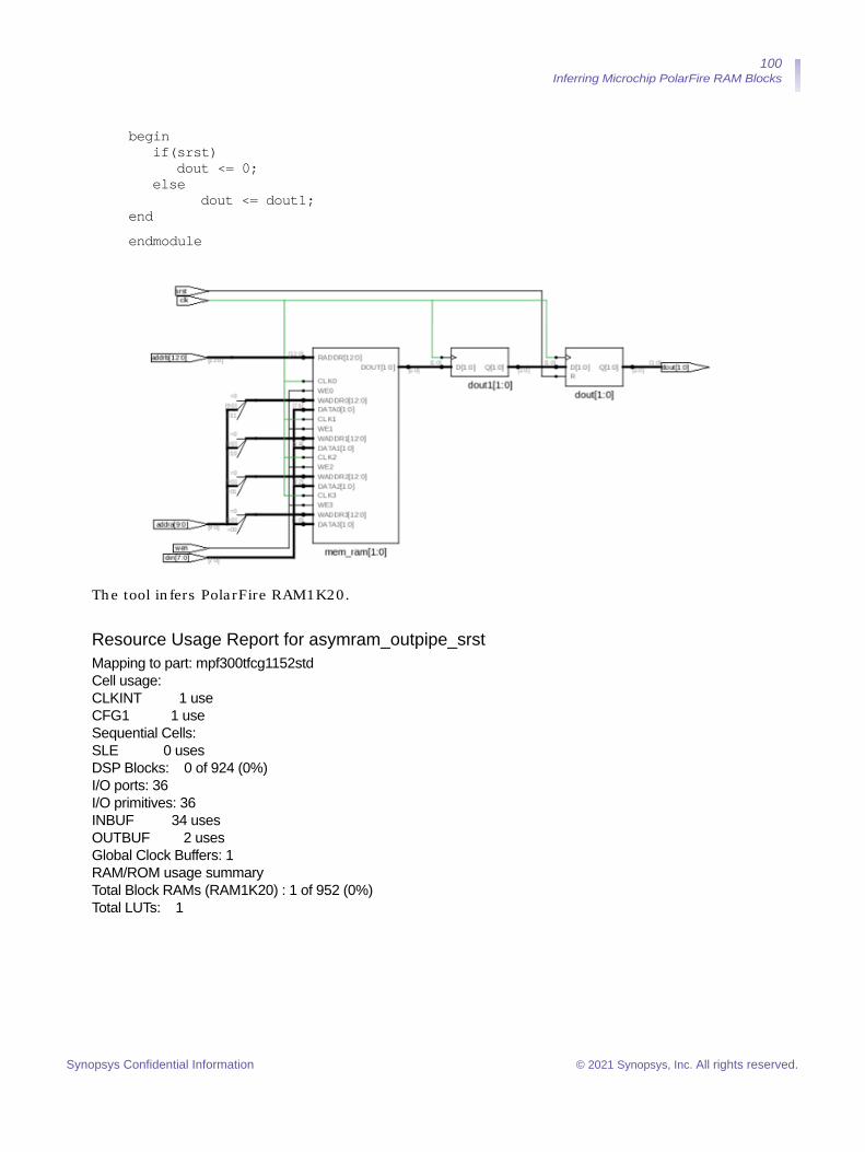
100 Inferring Microchip PolarFire RAM Blocks
begin if(srst)
dout <= 0; else
dout <= dout1; endendmodule
The tool infers PolarFire RAM1K20.
Resource Usage Report for asymram_outpipe_srst Mapping to part: mpf300tfcg1152std Cell usage: CLKINT 1 use CFG1 1 use Sequential Cells: SLE 0 uses DSP Blocks: 0 of 924 (0%) I/O ports: 36 I/O primitives: 36 INBUF 34 uses OUTBUF 2 uses Global Clock Buffers: 1 RAM/ROM usage summary Total Block RAMs (RAM1K20) : 1 of 952 (0%) Total LUTs: 1
Synopsys Confidential Information © 2021 Synopsys, Inc. All rights reserved.

101 Inferring Microchip PolarFire RAM Blocks
Example 58: VHDL Coding Style for Asymmetric RAM Inference for write_width > read_width
library IEEE; use IEEE.std_logic_1164.all; use IEEE.std_logic_unsigned.all;entity aram_ww_gt_rw is port (clk : in std_logic; ena : in std_logic; enb : in std_logic; wea : in std_logic; addra : in std_logic_vector (9 downto 0); addrb : in std_logic_vector (10 downto 0); din : in std_logic_vector (19 downto 0); dob : out std_logic_vector (9 downto 0)); end aram_ww_gt_rw;architecture syn of aram_ww_gt_rw is type ram_type is array (2047 downto 0) of std_logic_vector (9 downto 0) ; shared variable RAM : ram_type; begin
process (clk) begin
if clk'event and clk='1' then if ena = '1' then
if wea = '1' then RAM(conv_integer(addra & '0')) := din(9 downto 0); RAM(conv_integer(addra & '1')) := din(19 downto 10);end if;
end if; end if;
end process;process (clk) begin
if clk'event and clk='1' then if enb = '1' then
dob <= RAM(conv_integer(addrb)); end if;
end if; end process; end syn;
Synopsys Confidential Information © 2021 Synopsys, Inc. All rights reserved.
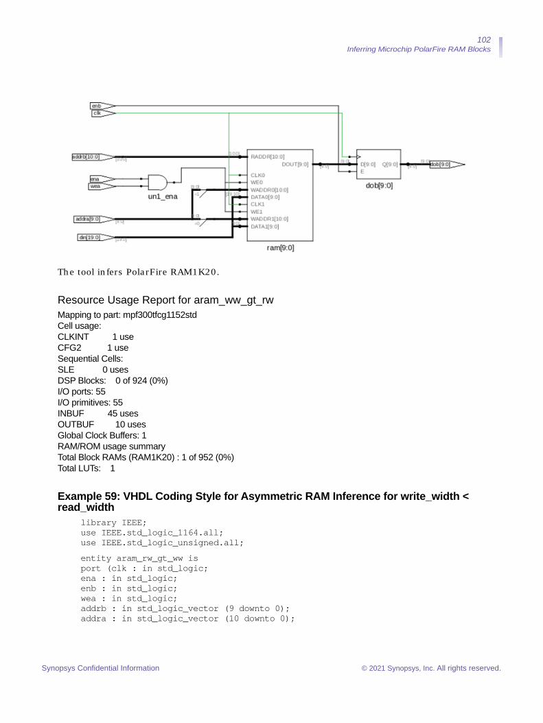
102 Inferring Microchip PolarFire RAM Blocks
The tool infers PolarFire RAM1K20.
Resource Usage Report for aram_ww_gt_rw Mapping to part: mpf300tfcg1152std Cell usage: CLKINT 1 use CFG2 1 use Sequential Cells: SLE 0 uses DSP Blocks: 0 of 924 (0%) I/O ports: 55 I/O primitives: 55 INBUF 45 uses OUTBUF 10 uses Global Clock Buffers: 1 RAM/ROM usage summary Total Block RAMs (RAM1K20) : 1 of 952 (0%) Total LUTs: 1
Example 59: VHDL Coding Style for Asymmetric RAM Inference for write_width < read_width
library IEEE; use IEEE.std_logic_1164.all; use IEEE.std_logic_unsigned.all;entity aram_rw_gt_ww is port (clk : in std_logic; ena : in std_logic; enb : in std_logic; wea : in std_logic; addrb : in std_logic_vector (9 downto 0); addra : in std_logic_vector (10 downto 0);
Synopsys Confidential Information © 2021 Synopsys, Inc. All rights reserved.
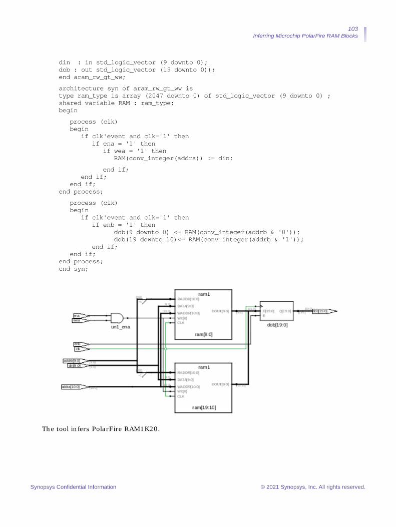
103 Inferring Microchip PolarFire RAM Blocks
din : in std_logic_vector (9 downto 0); dob : out std_logic_vector (19 downto 0)); end aram_rw_gt_ww;architecture syn of aram_rw_gt_ww is type ram_type is array (2047 downto 0) of std_logic_vector (9 downto 0) ; shared variable RAM : ram_type; begin
process (clk) begin
if clk'event and clk='1' then if ena = '1' then
if wea = '1' then RAM(conv_integer(addra)) := din;
end if; end if;
end if; end process;
process (clk) begin
if clk'event and clk='1' then if enb = '1' then
dob(9 downto 0) <= RAM(conv_integer(addrb & '0')); dob(19 downto 10)<= RAM(conv_integer(addrb & '1'));
end if; end if;
end process; end syn;
The tool infers PolarFire RAM1K20.
Synopsys Confidential Information © 2021 Synopsys, Inc. All rights reserved.
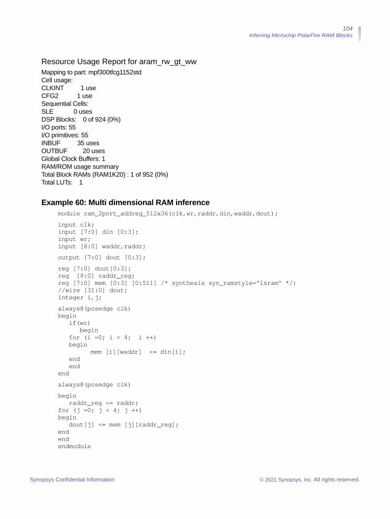
104 Inferring Microchip PolarFire RAM Blocks
Resource Usage Report for aram_rw_gt_ww Mapping to part: mpf300tfcg1152std Cell usage: CLKINT 1 use CFG2 1 use Sequential Cells: SLE 0 uses DSP Blocks: 0 of 924 (0%) I/O ports: 55 I/O primitives: 55 INBUF 35 uses OUTBUF 20 uses Global Clock Buffers: 1 RAM/ROM usage summary Total Block RAMs (RAM1K20) : 1 of 952 (0%) Total LUTs: 1
Example 60: Multi dimensional RAM inferencemodule ram_2port_addreg_512x36(clk,wr,raddr,din,waddr,dout); input clk; input [7:0] din [0:3]; input wr; input [8:0] waddr,raddr; output [7:0] dout [0:3]; reg [7:0] dout[0:3]; reg [8:0] raddr_reg; reg [7:0] mem [0:3] [0:511] /* synthesis syn_ramstyle="lsram" */; //wire [31:0] dout; integer i,j;always@(posedge clk) begin
if(wr) begin
for (i =0; i < 4; i ++) begin
mem [i][waddr] <= din[i]; end end
endalways@(posedge clk) begin
raddr_reg <= raddr; for (j =0; j < 4; j ++) begin
dout[j] <= mem [j][raddr_reg]; end end endmodule
Synopsys Confidential Information © 2021 Synopsys, Inc. All rights reserved.
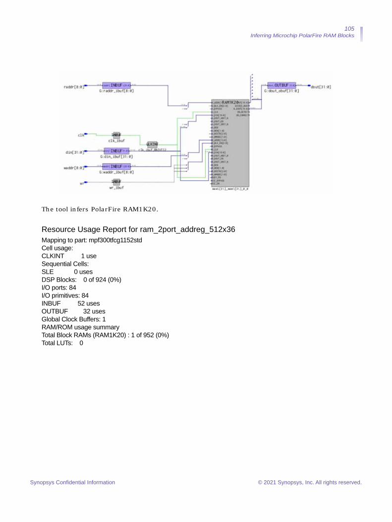
105 Inferring Microchip PolarFire RAM Blocks
The tool infers PolarFire RAM1K20.
Resource Usage Report for ram_2port_addreg_512x36 Mapping to part: mpf300tfcg1152std Cell usage: CLKINT 1 use Sequential Cells: SLE 0 uses DSP Blocks: 0 of 924 (0%) I/O ports: 84 I/O primitives: 84 INBUF 52 uses OUTBUF 32 uses Global Clock Buffers: 1 RAM/ROM usage summary Total Block RAMs (RAM1K20) : 1 of 952 (0%) Total LUTs: 0
Synopsys Confidential Information © 2021 Synopsys, Inc. All rights reserved.

106 Inferring Microchip PolarFire RAM Blocks
Inferring RAM Blocks for ROMThe following examples show how to infer the PolarFire RAM blocks for ROM:
• Example 61: ROM Inferred as LSRAM Using CASE Statement, on page 106
• Example 62: VHDL RTL Coding Style Using *.dat File (Memory File) and Synchronous Read for ROM Inferred as LSRAM Scenario, on page 108
• Example 63: RTL Coding Style Using *.dat File (Binary Memory File) and Synchronous Read for ROM Inferred as URAM Scenario, on page 109
• Example 64: RTL Coding Style Using *.dat File (Hexadecimal Memory Files) and Synchronous Read Using Enable for ROM Inferred as LSRAM Scenario, on page 111
• Example 65: RTL Coding Style Using *.dat File (Hexadecimal Memory Files) and Asynchronous Read for ROM Inferred as URAM, on page 112
• Example 66: VHDL RTL Coding Style Using WHEN Statement and Asynchronous Read for ROM Inferred as URAM Scenario, on page 114
• Example 67: Verilog RTL Coding Style for Dual Port with Multiple Clocks from Multiple ROM Blocks Inferred as LSRAMs, on page 116
Example 61: ROM Inferred as LSRAM Using CASE Statement
RTLmodule rom_infer_casestatement(clk,addr,dataout); input clk; parameter addr_width = 10; parameter data_width = 20; input [addr_width-1:0] addr; output [data_width-1:0] dataout; reg [data_width-1:0] dataout;always @ (posedge clk ) case (addr)10'd0 : dataout <= 20'b01000110000010001100; 10'd1 : dataout <= 20'b11100000110110011100; 10'd2 : dataout <= 20'b10110101101111011001; 10'd3 : dataout <= 20'b01111010011000000000; 10'd4 : dataout <= 20'b00110110100111111100; 10'd5 : dataout <= 20'b11110101000010001010; 10'd6 : dataout <= 20'b00010010110101000110; 10'd7 : dataout <= 20'b01001001010010100110; 10'd8 : dataout <= 20'b01110111000111111011; 10'd9 : dataout <= 20'b10010101111110111110; 10'd1015 : dataout <= 20'b11011010000111111101; 10'd1016 : dataout <= 20'b11001000101001110111; 10'd1017 : dataout <= 20'b01010000111100100011; 10'd1018 : dataout <= 20'b11000110011011011011; 10'd1019 : dataout <= 20'b10000000110101100110;
Synopsys Confidential Information © 2021 Synopsys, Inc. All rights reserved.

107 Inferring Microchip PolarFire RAM Blocks
10'd1020 : dataout <= 20'b11100101010001001011; 10'd1021 : dataout <= 20'b10010011000110001010; 10'd1022 : dataout <= 20'b00100000110010000101; 10'd1023 : dataout <= 20'b10001010000011111010; default : dataout <= 20'b00000000000000000000;endcase endmodule
SRS View (RTL)
SRM (Technology) View
Resource UsageSLE 0 uses Total Block RAMs (RAM1K20): 1 of 952 (0%) Total LUTs: 0
Synopsys Confidential Information © 2021 Synopsys, Inc. All rights reserved.
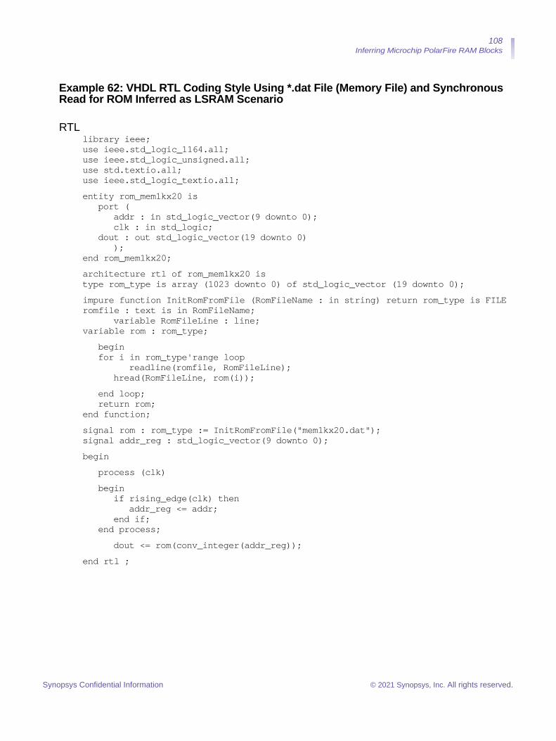
108 Inferring Microchip PolarFire RAM Blocks
Example 62: VHDL RTL Coding Style Using *.dat File (Memory File) and Synchronous Read for ROM Inferred as LSRAM Scenario
RTLlibrary ieee; use ieee.std_logic_1164.all; use ieee.std_logic_unsigned.all; use std.textio.all; use ieee.std_logic_textio.all;entity rom_mem1kx20 is
port ( addr : in std_logic_vector(9 downto 0); clk : in std_logic;
dout : out std_logic_vector(19 downto 0) );
end rom_mem1kx20;architecture rtl of rom_mem1kx20 is type rom_type is array (1023 downto 0) of std_logic_vector (19 downto 0);impure function InitRomFromFile (RomFileName : in string) return rom_type is FILE romfile : text is in RomFileName;
variable RomFileLine : line; variable rom : rom_type;
begin for i in rom_type'range loop
readline(romfile, RomFileLine); hread(RomFileLine, rom(i));
end loop; return rom;
end function;signal rom : rom_type := InitRomFromFile("mem1kx20.dat"); signal addr_reg : std_logic_vector(9 downto 0);begin process (clk) begin
if rising_edge(clk) then addr_reg <= addr;
end if; end process;
dout <= rom(conv_integer(addr_reg));end rtl ;
Synopsys Confidential Information © 2021 Synopsys, Inc. All rights reserved.
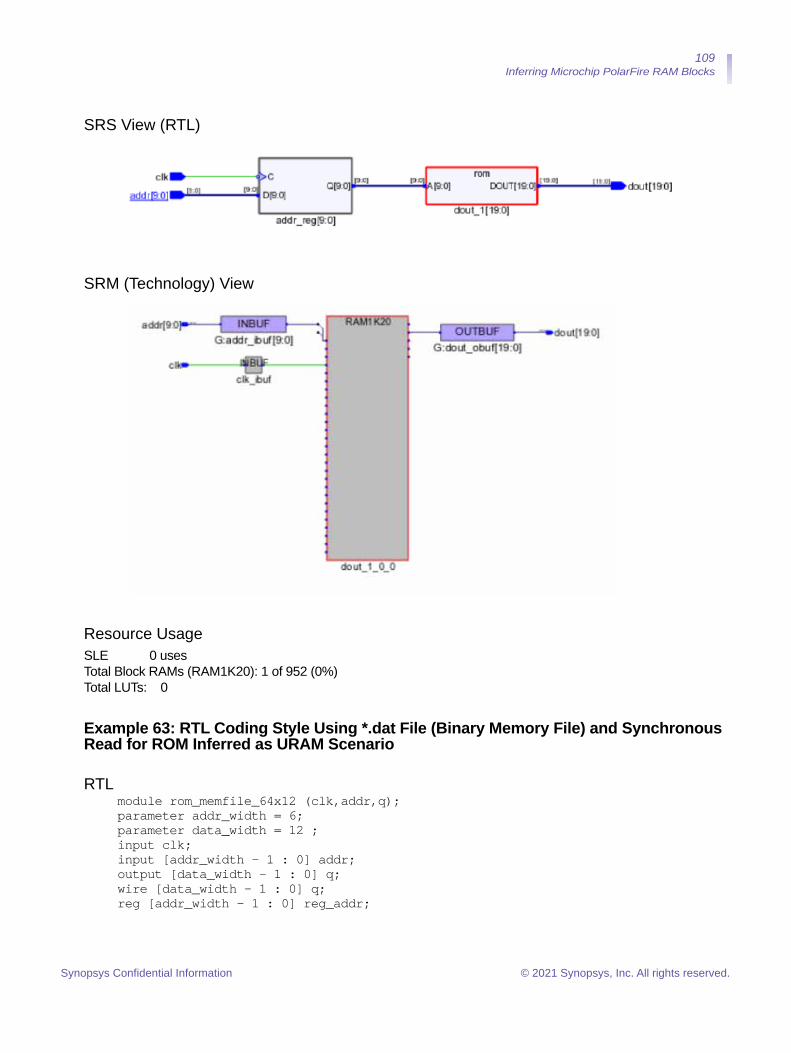
109 Inferring Microchip PolarFire RAM Blocks
SRS View (RTL)
SRM (Technology) View
Resource UsageSLE 0 uses Total Block RAMs (RAM1K20): 1 of 952 (0%) Total LUTs: 0
Example 63: RTL Coding Style Using *.dat File (Binary Memory File) and Synchronous Read for ROM Inferred as URAM Scenario
RTLmodule rom_memfile_64x12 (clk,addr,q); parameter addr_width = 6; parameter data_width = 12 ; input clk; input [addr_width - 1 : 0] addr; output [data_width - 1 : 0] q; wire [data_width - 1 : 0] q; reg [addr_width - 1 : 0] reg_addr;
Synopsys Confidential Information © 2021 Synopsys, Inc. All rights reserved.
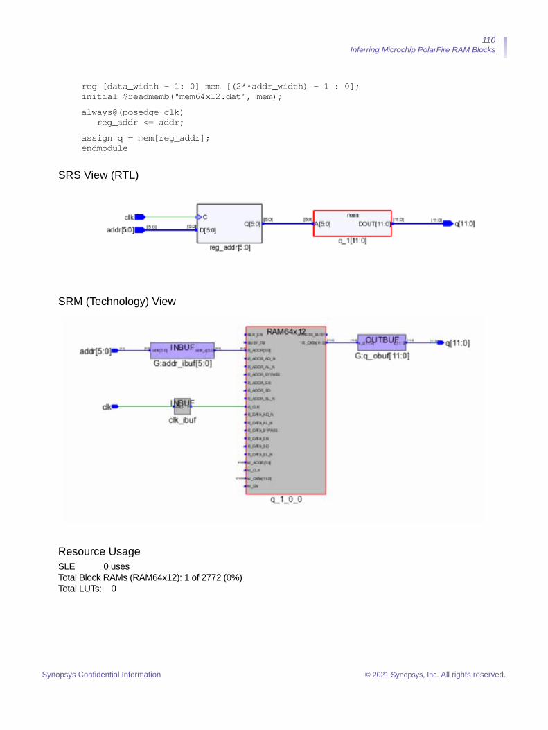
110 Inferring Microchip PolarFire RAM Blocks
reg [data_width - 1: 0] mem [(2**addr_width) - 1 : 0]; initial $readmemb("mem64x12.dat", mem);always@(posedge clk)
reg_addr <= addr;assign q = mem[reg_addr]; endmodule
SRS View (RTL)
SRM (Technology) View
Resource UsageSLE 0 uses Total Block RAMs (RAM64x12): 1 of 2772 (0%) Total LUTs: 0
Synopsys Confidential Information © 2021 Synopsys, Inc. All rights reserved.
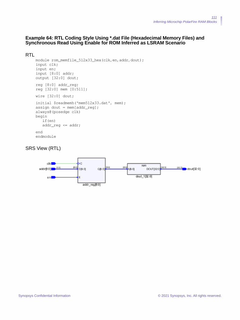
111 Inferring Microchip PolarFire RAM Blocks
Example 64: RTL Coding Style Using *.dat File (Hexadecimal Memory Files) and Synchronous Read Using Enable for ROM Inferred as LSRAM Scenario
RTLmodule rom_memfile_512x33_hex(clk,en,addr,dout); input clk; input en; input [8:0] addr; output [32:0] dout; reg [8:0] addr_reg; reg [32:0] mem [0:511];wire [32:0] dout;initial $readmemh("mem512x33.dat", mem); assign dout = mem[addr_reg]; always@(posedge clk) begin
if(en) addr_reg <= addr;
end endmodule
SRS View (RTL)
Synopsys Confidential Information © 2021 Synopsys, Inc. All rights reserved.

112 Inferring Microchip PolarFire RAM Blocks
SRM (Technology) View
Resource UsageSLE 34 uses Total Block RAMs (RAM1K20): 1 of 952 (0%) Total LUTs: 33
Example 65: RTL Coding Style Using *.dat File (Hexadecimal Memory Files) and Asynchronous Read for ROM Inferred as URAM
RTLmodule rom_memfile_1Kx64_async (addr,q);parameter addr_width = 10; parameter data_width = 64;input [addr_width - 1 : 0] addr; output [data_width - 1 : 0] q;wire [data_width - 1 : 0] q;reg [data_width - 1 : 0] mem [(2**addr_width) - 1 : 0]; initial $readmemh("mem1kx64.dat", mem); assign q = mem[addr];endmodule
Synopsys Confidential Information © 2021 Synopsys, Inc. All rights reserved.
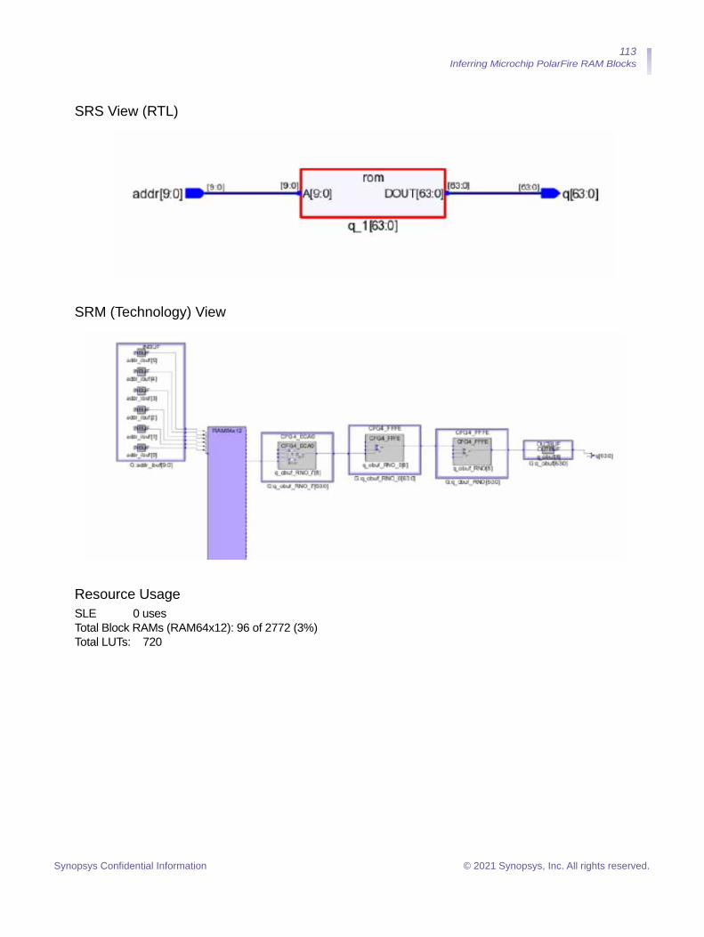
113 Inferring Microchip PolarFire RAM Blocks
SRS View (RTL)
SRM (Technology) View
Resource UsageSLE 0 uses Total Block RAMs (RAM64x12): 96 of 2772 (3%) Total LUTs: 720
Synopsys Confidential Information © 2021 Synopsys, Inc. All rights reserved.

114 Inferring Microchip PolarFire RAM Blocks
Example 66: VHDL RTL Coding Style Using WHEN Statement and Asynchronous Read for ROM Inferred as URAM Scenario
RTLlibrary IEEE; use IEEE.std_logic_1164.all;entity rom_infer_casestatement1 is
port( Q : out std_logic_vector(19 downto 0); A : in std_logic_vector(6 downto 0)
); end;architecture behav of rom_infer_casestatement1 is signal data : std_logic_vector(19 downto 0);begin
process(A) begin
case A is when "0000000" => data <= "10101010101011001010"; when "0000001" => data <= "11100101100011010101"; when "0000010" => data <= "10010110010010101010"; when "0000011" => data <= "11101100110101010001"; when "0000100" => data <= "11111011010101010001"; when "0000101" => data <= "11110101010101010011"; when "0000110" => data <= "10101001100110101011"; when "0000111" => data <= "10110101001101010100"; when "0001000" => data <= "00100110011010101010"; when "0001001" => data <= "00101100110101010010"; when "0001010" => data <= "01100110011010101010"; when "0001011" => data <= "10111101010100101011"; when "0001100" => data <= "01011101010100101011"; when "0001101" => data <= "11001010101010110101"; when "0001110" => data <= "00100101010101101001"; when "0001111" => data <= "11011010101010001010"; when "0011001" => data <= "00101100101010101010"; when "0101010" => data <= "01101010101001100110"; when "0011011" => data <= "10111010101010101011"; when "0101100" => data <= "01011010100110101101"; when "0101101" => data <= "11001101010100110101"; when "1001110" => data <= "00100110010110101010"; when "0101111" => data <= "11011000111010100100"; when "1000111" => data <= "10110101001101010100"; when "1001000" => data <= "00100110011010101010"; when "1001001" => data <= "00101100110101010010"; when "1001010" => data <= "01100110011010101010"; when "0101011" => data <= "10111101010100101011"; when others => data <= "11011000111010100100";
end case;end process;
Q <= data;end;
Synopsys Confidential Information © 2021 Synopsys, Inc. All rights reserved.

115 Inferring Microchip PolarFire RAM Blocks
SRS View (RTL)
SRM (Technology) View
Resource UsageSLE 0 uses Total Block RAMs (RAM64x12) : 4 of 2772 (0%) Total LUTs: 20
Synopsys Confidential Information © 2021 Synopsys, Inc. All rights reserved.
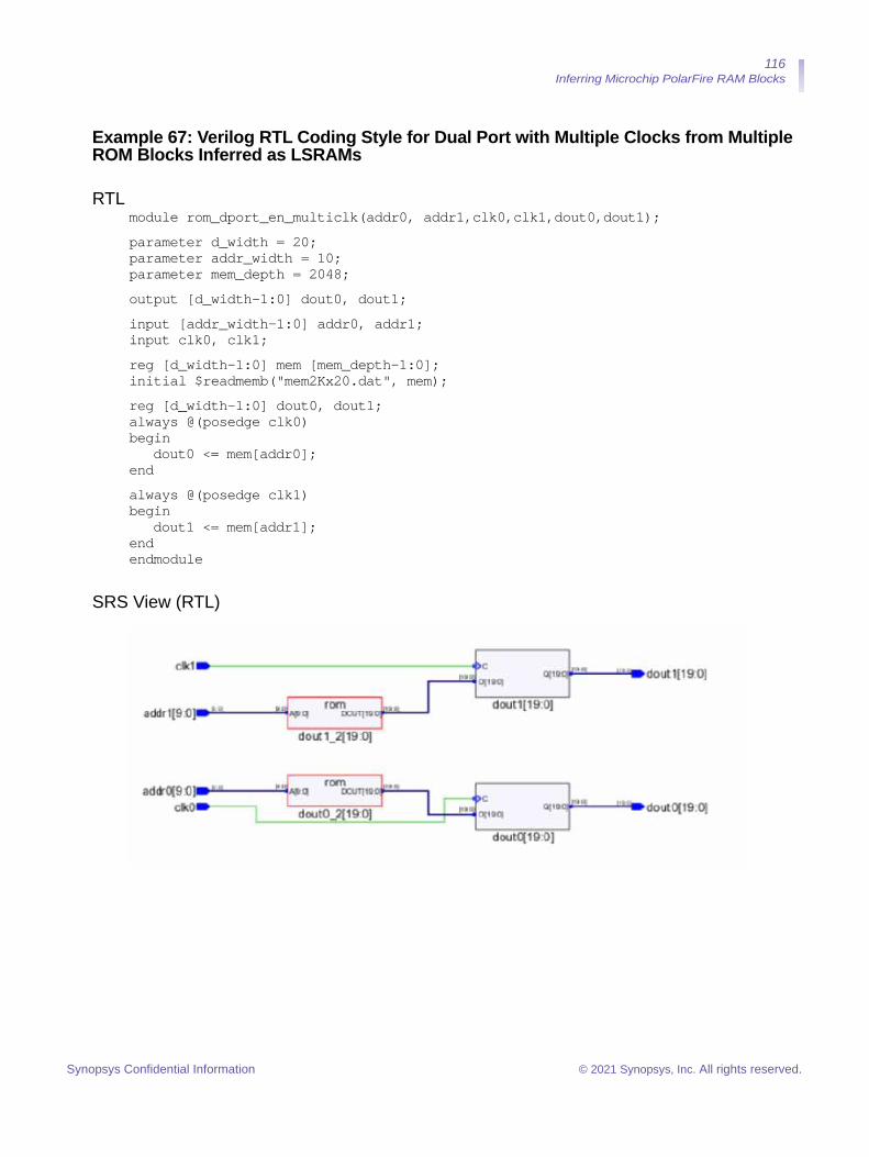
116 Inferring Microchip PolarFire RAM Blocks
Example 67: Verilog RTL Coding Style for Dual Port with Multiple Clocks from Multiple ROM Blocks Inferred as LSRAMs
RTLmodule rom_dport_en_multiclk(addr0, addr1,clk0,clk1,dout0,dout1);parameter d_width = 20; parameter addr_width = 10; parameter mem_depth = 2048; output [d_width-1:0] dout0, dout1;input [addr_width-1:0] addr0, addr1; input clk0, clk1; reg [d_width-1:0] mem [mem_depth-1:0]; initial $readmemb("mem2Kx20.dat", mem);reg [d_width-1:0] dout0, dout1; always @(posedge clk0) begin
dout0 <= mem[addr0]; end always @(posedge clk1) begin
dout1 <= mem[addr1]; end endmodule
SRS View (RTL)
Synopsys Confidential Information © 2021 Synopsys, Inc. All rights reserved.
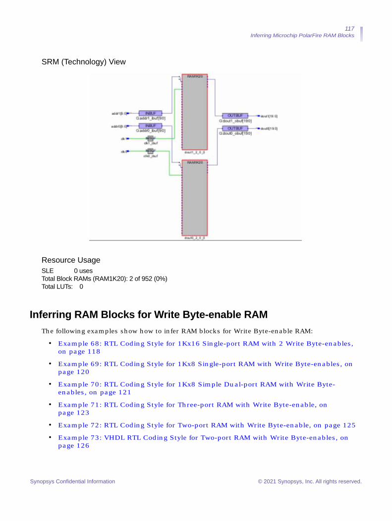
117 Inferring Microchip PolarFire RAM Blocks
SRM (Technology) View
Resource UsageSLE 0 uses Total Block RAMs (RAM1K20): 2 of 952 (0%) Total LUTs: 0
Inferring RAM Blocks for Write Byte-enable RAMThe following examples show how to infer RAM blocks for Write Byte-enable RAM:
• Example 68: RTL Coding Style for 1Kx16 Single-port RAM with 2 Write Byte-enables, on page 118
• Example 69: RTL Coding Style for 1Kx8 Single-port RAM with Write Byte-enables, on page 120
• Example 70: RTL Coding Style for 1Kx8 Simple Dual-port RAM with Write Byte-enables, on page 121
• Example 71: RTL Coding Style for Three-port RAM with Write Byte-enable, on page 123
• Example 72: RTL Coding Style for Two-port RAM with Write Byte-enable, on page 125
• Example 73: VHDL RTL Coding Style for Two-port RAM with Write Byte-enables, on page 126
Synopsys Confidential Information © 2021 Synopsys, Inc. All rights reserved.
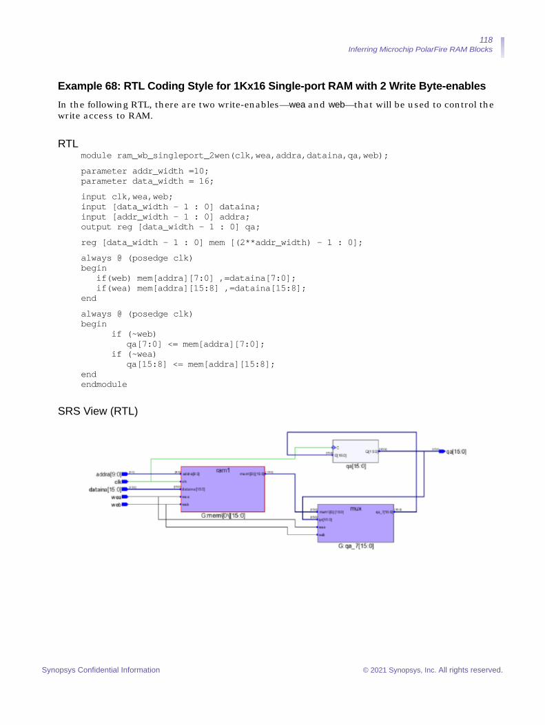
118 Inferring Microchip PolarFire RAM Blocks
Example 68: RTL Coding Style for 1Kx16 Single-port RAM with 2 Write Byte-enablesIn the following RTL, there are two write-enables—wea and web—that will be used to control the write access to RAM.
RTLmodule ram_wb_singleport_2wen(clk,wea,addra,dataina,qa,web);parameter addr_width =10; parameter data_width = 16;input clk,wea,web; input [data_width - 1 : 0] dataina; input [addr_width - 1 : 0] addra; output reg [data_width - 1 : 0] qa;reg [data_width - 1 : 0] mem [(2**addr_width) - 1 : 0];always @ (posedge clk) begin
if(web) mem[addra][7:0] ,=dataina[7:0]; if(wea) mem[addra][15:8] ,=dataina[15:8];
endalways @ (posedge clk) begin
if (~web) qa[7:0] <= mem[addra][7:0];
if (~wea) qa[15:8] <= mem[addra][15:8];
end endmodule
SRS View (RTL)
Synopsys Confidential Information © 2021 Synopsys, Inc. All rights reserved.
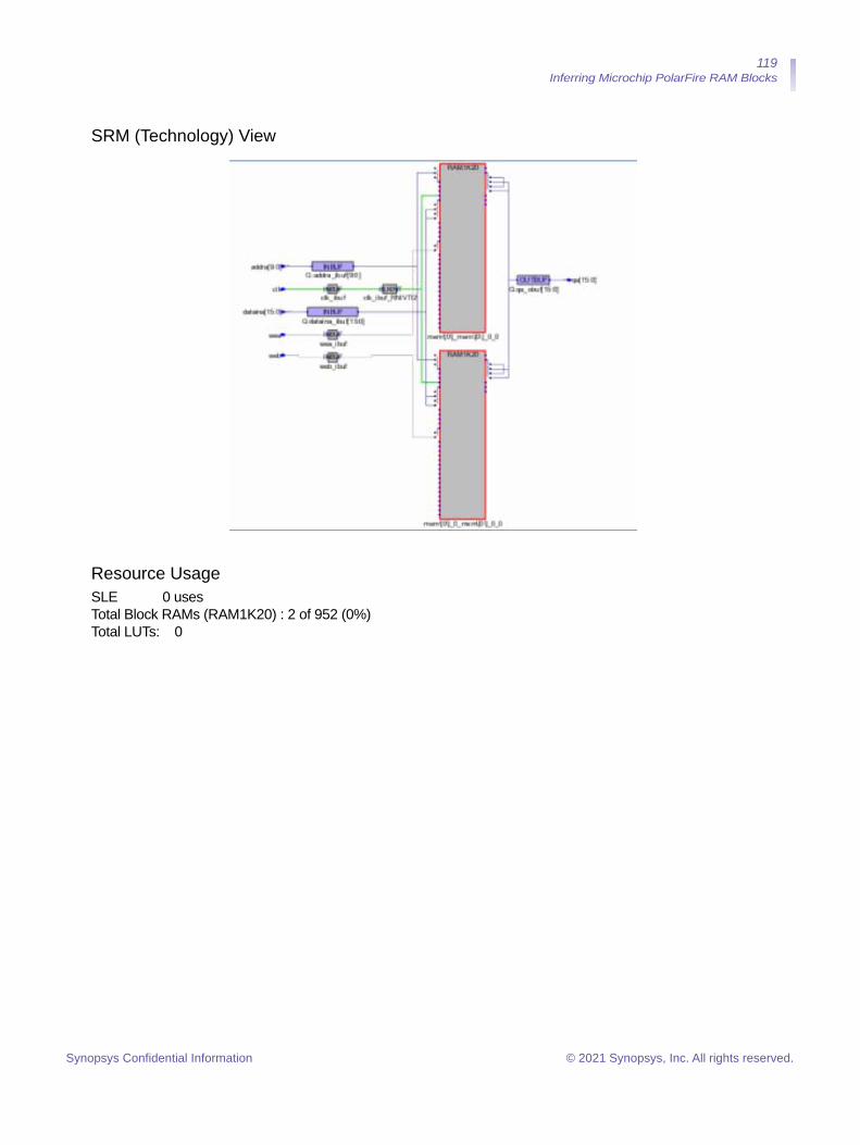
119 Inferring Microchip PolarFire RAM Blocks
SRM (Technology) View
Resource UsageSLE 0 uses Total Block RAMs (RAM1K20) : 2 of 952 (0%) Total LUTs: 0
Synopsys Confidential Information © 2021 Synopsys, Inc. All rights reserved.
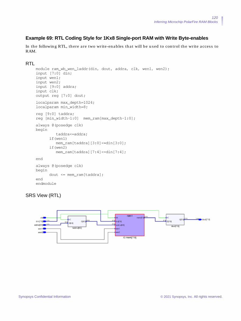
120 Inferring Microchip PolarFire RAM Blocks
Example 69: RTL Coding Style for 1Kx8 Single-port RAM with Write Byte-enablesIn the following RTL, there are two write-enables that will be used to control the write access to RAM.
RTLmodule ram_wb_wen_1addr(din, dout, addra, clk, wen1, wen2); input [7:0] din; input wen1; input wen2; input [9:0] addra; input clk; output reg [7:0] dout;localparam max_depth=1024; localparam min_width=8;reg [9:0] taddra; reg [min_width-1:0] mem_ram[max_depth-1:0];always @(posedge clk) begin
taddra<=addra; if(wen1)
mem_ram[taddra][3:0]<=din[3:0]; if(wen2)
mem_ram[taddra][7:4]<=din[7:4];endalways @(posedge clk) begin
dout <= mem_ram[taddra]; end endmodule
SRS View (RTL)
Synopsys Confidential Information © 2021 Synopsys, Inc. All rights reserved.
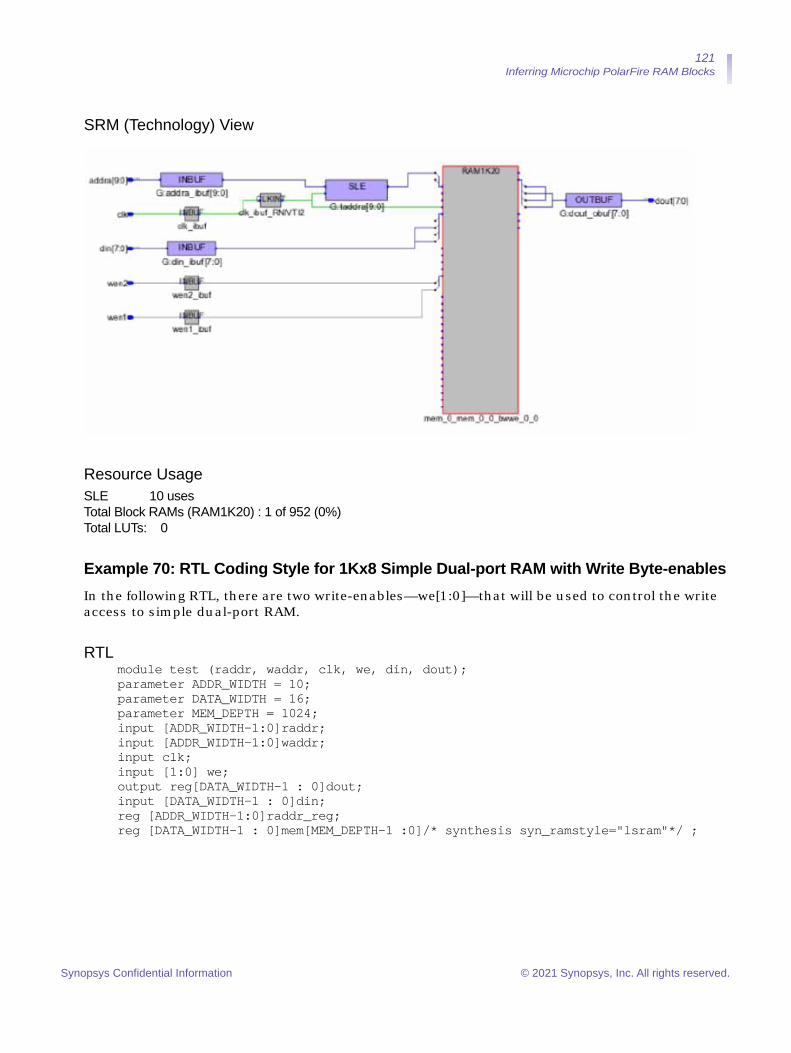
121 Inferring Microchip PolarFire RAM Blocks
SRM (Technology) View
Resource UsageSLE 10 uses Total Block RAMs (RAM1K20) : 1 of 952 (0%) Total LUTs: 0
Example 70: RTL Coding Style for 1Kx8 Simple Dual-port RAM with Write Byte-enablesIn the following RTL, there are two write-enables—we[1:0]—that will be used to control the write access to simple dual-port RAM.
RTLmodule test (raddr, waddr, clk, we, din, dout); parameter ADDR_WIDTH = 10; parameter DATA_WIDTH = 16; parameter MEM_DEPTH = 1024; input [ADDR_WIDTH-1:0]raddr; input [ADDR_WIDTH-1:0]waddr; input clk; input [1:0] we; output reg[DATA_WIDTH-1 : 0]dout; input [DATA_WIDTH-1 : 0]din; reg [ADDR_WIDTH-1:0]raddr_reg; reg [DATA_WIDTH-1 : 0]mem[MEM_DEPTH-1 :0]/* synthesis syn_ramstyle="lsram"*/ ;
Synopsys Confidential Information © 2021 Synopsys, Inc. All rights reserved.
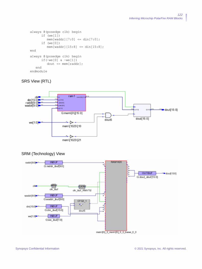
122 Inferring Microchip PolarFire RAM Blocks
always @(posedge clk) begin if (we[1])
mem[waddr][7:0] <= din[7:0]; if (we[0])
mem[waddr][15:8] <= din[15:8]; endalways @(posedge clk) begin
if(~we[0] & ~we[1]) dout <= mem[raddr];
end endmodule
SRS View (RTL)
SRM (Technology) View
Synopsys Confidential Information © 2021 Synopsys, Inc. All rights reserved.
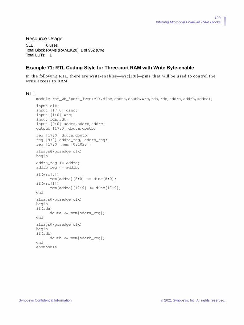
123 Inferring Microchip PolarFire RAM Blocks
Resource UsageSLE 0 uses Total Block RAMs (RAM1K20): 1 of 952 (0%) Total LUTs: 1
Example 71: RTL Coding Style for Three-port RAM with Write Byte-enableIn the following RTL, there are write-enables—wrc[1:0]—pins that will be used to control the write access to RAM.
RTLmodule ram_wb_3port_1wen(clk,dinc,douta,doutb,wrc,rda,rdb,addra,addrb,addrc);input clk; input [17:0] dinc; input [1:0] wrc; input rda,rdb; input [9:0] addra,addrb,addrc; output [17:0] douta,doutb;reg [17:0] douta,doutb; reg [9:0] addra_reg, addrb_reg; reg [17:0] mem [0:1023];always@(posedge clk) beginaddra_reg <= addra; addrb_reg <= addrb;if(wrc[0])
mem[addrc][8:0] <= dinc[8:0]; if(wrc[1])
mem[addrc][17:9] <= dinc[17:9]; endalways@(posedge clk) begin if(rda)
douta <= mem[addra_reg]; endalways@(posedge clk) begin if(rdb)
doutb <= mem[addrb_reg]; end endmodule
Synopsys Confidential Information © 2021 Synopsys, Inc. All rights reserved.
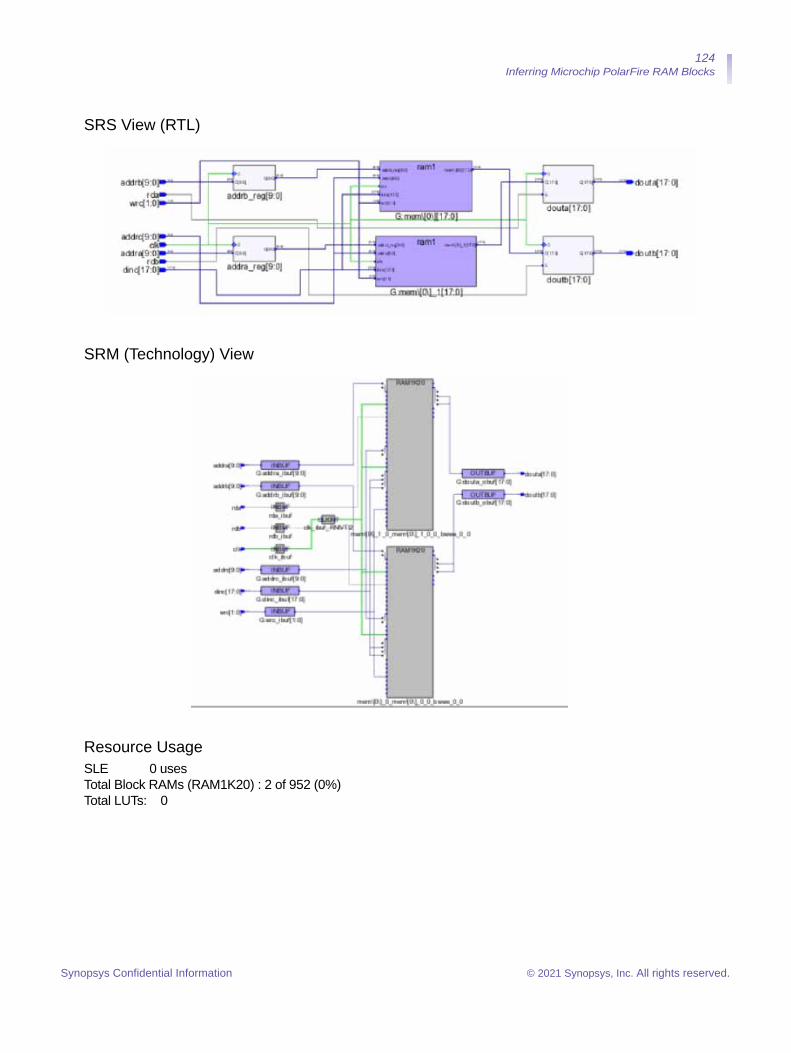
124 Inferring Microchip PolarFire RAM Blocks
SRS View (RTL)
SRM (Technology) View
Resource UsageSLE 0 uses Total Block RAMs (RAM1K20) : 2 of 952 (0%) Total LUTs: 0
Synopsys Confidential Information © 2021 Synopsys, Inc. All rights reserved.
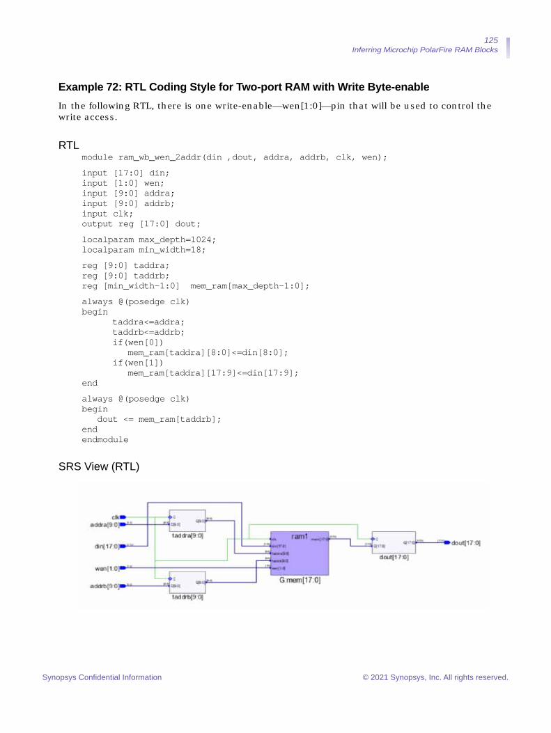
125 Inferring Microchip PolarFire RAM Blocks
Example 72: RTL Coding Style for Two-port RAM with Write Byte-enableIn the following RTL, there is one write-enable—wen[1:0]—pin that will be used to control the write access.
RTLmodule ram_wb_wen_2addr(din ,dout, addra, addrb, clk, wen);input [17:0] din; input [1:0] wen; input [9:0] addra; input [9:0] addrb; input clk; output reg [17:0] dout;localparam max_depth=1024; localparam min_width=18;reg [9:0] taddra; reg [9:0] taddrb; reg [min_width-1:0] mem_ram[max_depth-1:0];always @(posedge clk) begin
taddra<=addra; taddrb<=addrb; if(wen[0])
mem_ram[taddra][8:0]<=din[8:0]; if(wen[1])
mem_ram[taddra][17:9]<=din[17:9]; endalways @(posedge clk) begin
dout <= mem_ram[taddrb]; end endmodule
SRS View (RTL)
Synopsys Confidential Information © 2021 Synopsys, Inc. All rights reserved.
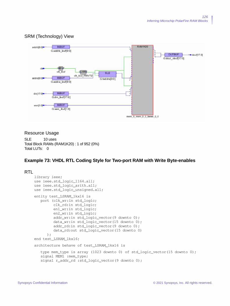
126 Inferring Microchip PolarFire RAM Blocks
SRM (Technology) View
Resource UsageSLE 10 uses Total Block RAMs (RAM1K20) : 1 of 952 (0%) Total LUTs: 0
Example 73: VHDL RTL Coding Style for Two-port RAM with Write Byte-enables
RTLlibrary ieee; use ieee.std_logic_1164.all; use ieee.std_logic_arith.all; use ieee.std_logic_unsigned.all;entity test_LSRAM_1kx16 is
port (clk_wr:in std_logic; clk_rd:in std_logic; en1_wr:in std_logic; en2_wr:in std_logic; addr_wr:in std_logic_vector(9 downto 0); data_wr:in std_logic_vector(15 downto 0); addr_rd:in std_logic_vector(9 downto 0); data_rd:out std_logic_vector(15 downto 0)
); end test_LSRAM_1kx16;architecture behave of test_LSRAM_1kx16 is
type mem_type is array (1023 downto 0) of std_logic_vector(15 downto 0); signal MEM1 :mem_type; signal r_addr_rd :std_logic_vector(9 downto 0);
Synopsys Confidential Information © 2021 Synopsys, Inc. All rights reserved.

127 Inferring Microchip PolarFire RAM Blocks
begin process(clk_wr) begin
if rising_edge(clk_wr) thenif (en1_wr = '1') then
MEM1(CONV_INTEGER(addr_wr(9 downto 0)))(7 downto 0)<= data_wr(7 downto 0); end if;
if (en2_wr = '1') then
MEM1(CONV_INTEGER(addr_wr(9 downto 0)))(15 downto 8) <= data_wr(15 downto 8); end if;
end if; end process;data_rd <= MEM1(CONV_INTEGER(r_addr_rd));process(clk_rd) begin
if rising_edge(clk_rd) then r_addr_rd <= addr_rd;
end if;end process;
end behave;
SRS View (RTL)
Synopsys Confidential Information © 2021 Synopsys, Inc. All rights reserved.

128 Inferring Microchip PolarFire RAM Blocks
SRM (Technology) View
Resource UsageSLE 0 uses Total Block RAMs (RAM1K20): 1 of 952 (0%) Total LUTs: 0
Inferring Initialized RAM blocksThe following examples illustrate the RAM initialization feature.
• Example 74: Verilog RTL Coding Style for Inferring LSRAM/URAM Initialized Using readmemb Statement, on page 129
• Example 75: Verilog RTL Coding Style for Inferring LSRAM/URAM Initialized Through Array Initialization Statement, on page 129
• Example 76: Verilog RTL Coding Style for Inferring LSRAM/URAM Initialized Through Array Initialization Statement with Index Numbers, on page 130
• Example 77: VHDL RTL Coding Style for Inferring LSRAM/URAM Initialized Through Array Initialization, on page 130
Synopsys Confidential Information © 2021 Synopsys, Inc. All rights reserved.

129 Inferring Microchip PolarFire RAM Blocks
Example 74: Verilog RTL Coding Style for Inferring LSRAM/URAM Initialized Using readmemb StatementRAM gets initialized from the mem1.dat file using the readmemb system task for the RTL code below. The data file mem1.dat must reside in the same directory as the RTL file for the given example.
RTLmodule test (clk,we,addr,din,q); parameter addr_width = 9; parameter data_width = 10; input clk,we; input [addr_width - 1 : 0] addr; input [data_width - 1 : 0] din; output [data_width - 1 : 0] q; reg [data_width - 1 : 0] q; reg [data_width - 1 : 0] mem [(2**addr_width) - 1 : 0]; initial $readmemb("mem1.dat", mem); always @ (posedge clk)
if(we) mem[addr] <= din; always @ (posedge clk )
if(~we) q <= mem[addr]; endmodule
Example 75: Verilog RTL Coding Style for Inferring LSRAM/URAM Initialized Through Array Initialization StatementArray initialization statement in the RTL below is a System Verilog construct. Hence, the System Verilog option needs to be enabled in the Verilog tab of the Implementation Options dialog box in the Synplify Pro user interface before running synthesis.
RTLmodule test (clk,we,addr,din,q); parameter addr_width = 3; parameter data_width = 12; input clk,we; input [addr_width - 1 : 0] addr; input [data_width - 1 : 0] din; output [data_width - 1 : 0] q; reg [data_width - 1 : 0] q; reg [data_width - 1 : 0] mem [(2**addr_width) - 1 : 0] = {12'h1, 12'h2, 12'h3, 12'h4, 12'h5, 12'h6, 12'h7, 12'h8}; always @ (posedge clk)
if(we) mem[addr] <= din; always @ (posedge clk )
if(~we) q <= mem[addr]; endmodule
Synopsys Confidential Information © 2021 Synopsys, Inc. All rights reserved.
130 Inferring Microchip PolarFire RAM Blocks
Example 76: Verilog RTL Coding Style for Inferring LSRAM/URAM Initialized Through Array Initialization Statement with Index NumbersArray initialization statement using index numbers, in the RTL below, is a System Verilog construct. Hence, the System Verilog option needs to be enabled in the Verilog tab of the Implementation Options dialog box in the Synplify Pro user interface before running synthesis.
RTLmodule ram_memfile_2Kx20_intialRTL(clk,addr,q,we,din); parameter addr_width = 10; parameter data_width = 20; input clk,we; input [addr_width - 1 : 0] addr; input [data_width - 1 : 0] din; output [data_width - 1 : 0] q; wire [data_width - 1 : 0] q; reg [addr_width - 1 : 0] reg_addr; reg [data_width - 1 : 0] mem [(2**addr_width) - 1 : 0] = '{0:20'h34343,1:20'h5555,default:0}; always@(posedge clk) begin
reg_addr <= addr; if(we)
mem[addr] <= din; end assign q = mem[reg_addr]; endmodule
Example 77: VHDL RTL Coding Style for Inferring LSRAM/URAM Initialized Through Array Initialization
RTLlibrary ieee; use ieee.std_logic_1164.all; use ieee.std_logic_unsigned.all; entity test is port (clk1 : in std_logic; clk2 : in std_logic; we : in std_logic; addr1 : in std_logic_vector(7 downto 0); addr2 : in std_logic_vector(7 downto 0); di : in std_logic_vector(15 downto 0); do1 : out std_logic_vector(15 downto 0); do2 : out std_logic_vector(15 downto 0)); end test; architecture syn of test is type ram_type is array (255 downto 0) of std_logic_vector (15 downto 0); signal RAM : ram_type:= (255 downto 100 => X"B8B8", 99 downto 0 => X"8282"); begin process (clk1) begin if rising_edge(clk1) then if we = '1' then RAM(conv_integer(addr1)) <= di; end if; do1 <= RAM(conv_integer(addr1)); end if; end process;
Synopsys Confidential Information © 2021 Synopsys, Inc. All rights reserved.
131 Inferring Microchip PolarFire RAM Blocks
process (clk2) begin if rising_edge(clk2) then do2 <= RAM(conv_integer(addr2)); end if; end process; end syn;
Inferring RAM Blocks for SeqshiftThe seqshift primitive in the compiler is usually mapped to the URAM when both the following conditions are met:
• Depth >= DEPTH_THRESHOLD
• Depth * Width >= (DEPTH * WIDTH)threshold
For PolarFire devices, the threshold values are:
• DEPTH_THRESHOLD = 4
• (DEPTH * WIDTH)threshold = 36
You can convert Seqshift to URAM using any of the following options:
• By configuring set_option -seqshift_to_uram 1 in the project file. The URAM is inferred if the threshold for the Polarfire device is met.
• By applying attribute syn_srlstyle="uram" on seqshift instance in RTL. The URAM is inferred irrespective of the size of the seqshift instance.
• By applying attribute syn_srlstyle="uram" globally in the RTL or the FDC file. The URAM is inferred if the threshold for the Polarfire device is met.
The Synplify Pro compiler infers a seqshift primitive for the following RTL coding styles:
• Example 78: URAM Inference for Seqshift, on page 132
• Example 79: URAM Inference for Seqshift with Reset, on page 134
• Example 80: URAM Inference for Seqshift with Dynamic Stage Output, on page 136
• Example 81: URAM Inference for Seqshift with Both Synchronous and Asynchronous Reset, on page 138
• Example 82: Single port RAM with syn_ramstyle = "low_power" and global power option is off, on page 140
• Example 83: Single port RAM with syn_ramstyle = "no_low_power" and global power option is on, on page 143
Synopsys Confidential Information © 2021 Synopsys, Inc. All rights reserved.
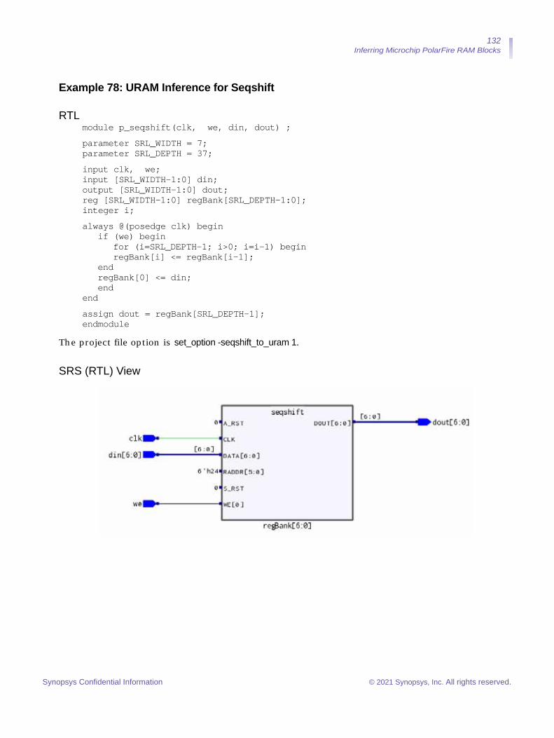
132 Inferring Microchip PolarFire RAM Blocks
Example 78: URAM Inference for Seqshift
RTLmodule p_seqshift(clk, we, din, dout) ; parameter SRL_WIDTH = 7; parameter SRL_DEPTH = 37; input clk, we; input [SRL_WIDTH-1:0] din; output [SRL_WIDTH-1:0] dout; reg [SRL_WIDTH-1:0] regBank[SRL_DEPTH-1:0]; integer i; always @(posedge clk) begin
if (we) begin for (i=SRL_DEPTH-1; i>0; i=i-1) begin regBank[i] <= regBank[i-1];
end regBank[0] <= din; end
end assign dout = regBank[SRL_DEPTH-1]; endmodule
The project file option is set_option -seqshift_to_uram 1.
SRS (RTL) View
Synopsys Confidential Information © 2021 Synopsys, Inc. All rights reserved.
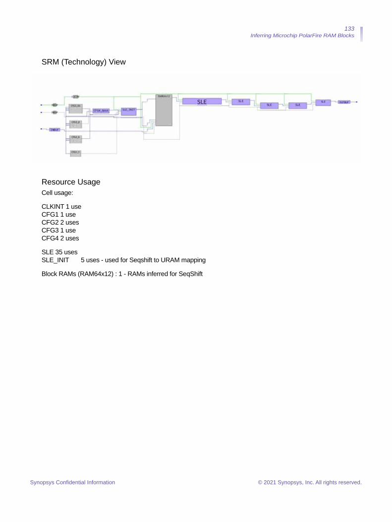
133 Inferring Microchip PolarFire RAM Blocks
SRM (Technology) View
Resource UsageCell usage:
CLKINT 1 use CFG1 1 use CFG2 2 uses CFG3 1 use CFG4 2 uses
SLE 35 uses SLE_INIT 5 uses - used for Seqshift to URAM mapping
Block RAMs (RAM64x12) : 1 - RAMs inferred for SeqShift
Synopsys Confidential Information © 2021 Synopsys, Inc. All rights reserved.

134 Inferring Microchip PolarFire RAM Blocks
Example 79: URAM Inference for Seqshift with ResetThe Seqshift with reset (synchronous/asynchronous) is implemented using the URAM.
RTLmodule p_seqshift(clk, a_rst, we, din, dout) ; parameter SRL_WIDTH = 7; parameter SRL_DEPTH = 37; input clk, a_rst, we; input [SRL_WIDTH-1:0] din; output [SRL_WIDTH-1:0] dout; reg [SRL_WIDTH-1:0] regBank[SRL_DEPTH-1:0]; integer i; always @(posedge clk or posedge a_rst) begin
if (a_rst) begin for(i = 0; i <= SRL_DEPTH-1; i = i+1)
regBank[i] <= {(SRL_WIDTH){1'b0}}; end
else if (we) begin for (i=SRL_DEPTH-1; i>0; i=i-1) begin
regBank[i] <= regBank[i-1]; end regBank[0] <= din;
end end assign dout = regBank[SRL_DEPTH-1]; endmodule
The project file option is set_option -seqshift_to_uram 1.
SRS (RTL) View
Synopsys Confidential Information © 2021 Synopsys, Inc. All rights reserved.

135 Inferring Microchip PolarFire RAM Blocks
SRM (Technology) View
Resource UsageCell usage: CLKINT 1 use CFG1 2 uses CFG2 10 uses CFG3 9 uses CFG4 66 uses
SLE 67 uses SLE_INIT 5 uses - used for Seqshift to URAM mapping
Block RAMs (RAM64x12) : 1 - RAMs inferred for SeqShift
Synopsys Confidential Information © 2021 Synopsys, Inc. All rights reserved.
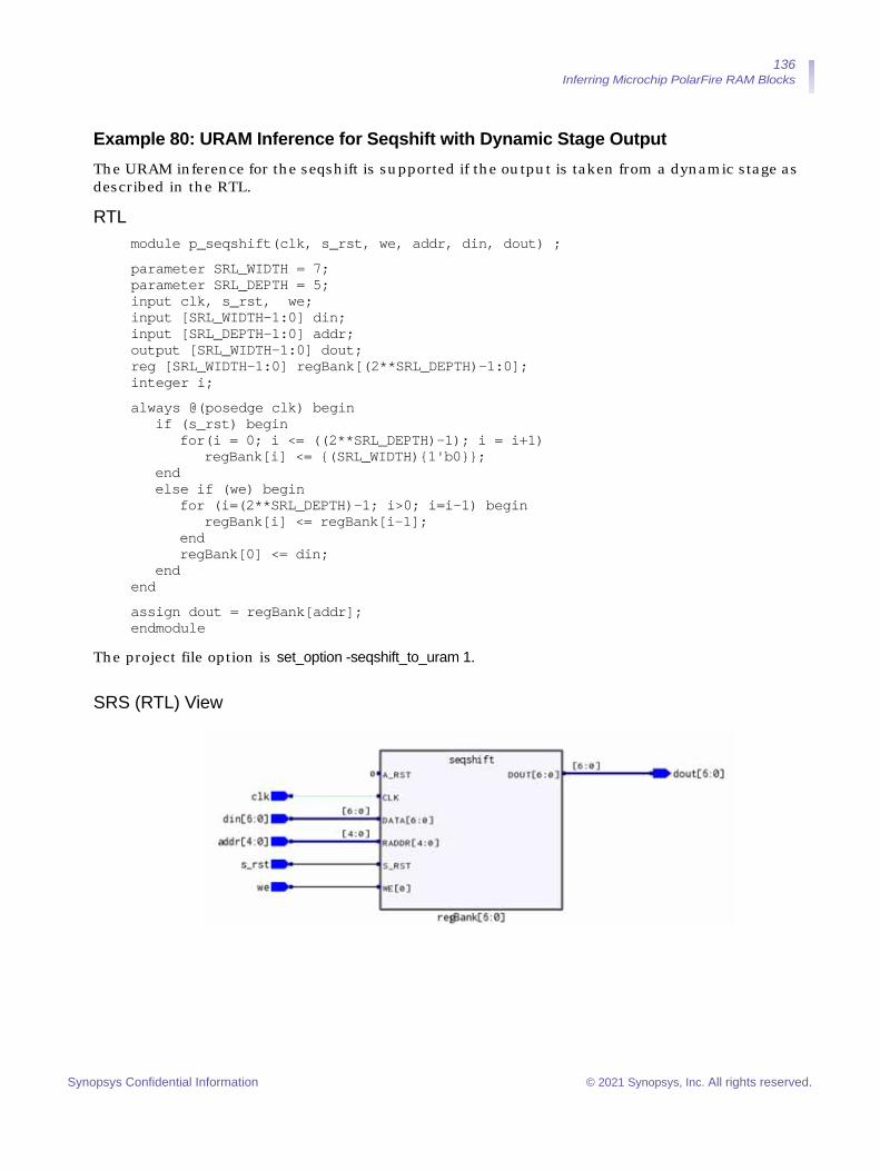
136 Inferring Microchip PolarFire RAM Blocks
Example 80: URAM Inference for Seqshift with Dynamic Stage OutputThe URAM inference for the seqshift is supported if the output is taken from a dynamic stage as described in the RTL.
RTLmodule p_seqshift(clk, s_rst, we, addr, din, dout) ; parameter SRL_WIDTH = 7; parameter SRL_DEPTH = 5; input clk, s_rst, we; input [SRL_WIDTH-1:0] din; input [SRL_DEPTH-1:0] addr; output [SRL_WIDTH-1:0] dout; reg [SRL_WIDTH-1:0] regBank[(2**SRL_DEPTH)-1:0]; integer i; always @(posedge clk) begin
if (s_rst) begin for(i = 0; i <= ((2**SRL_DEPTH)-1); i = i+1)
regBank[i] <= {(SRL_WIDTH){1'b0}}; end else if (we) begin
for (i=(2**SRL_DEPTH)-1; i>0; i=i-1) begin regBank[i] <= regBank[i-1];
end regBank[0] <= din;
end end assign dout = regBank[addr]; endmodule
The project file option is set_option -seqshift_to_uram 1.
SRS (RTL) View
Synopsys Confidential Information © 2021 Synopsys, Inc. All rights reserved.

137 Inferring Microchip PolarFire RAM Blocks
SRM (Technology) View
Resource UsageCell usage: CLKINT 1 use CFG1 2 uses CFG2 59 uses CFG3 16 uses CFG4 87 uses
SLE 32 uses SLE_INIT 5 uses - used for Seqshift to URAM mapping
Block RAMs (RAM64x12) : 1 - RAMs inferred for SeqShift
Synopsys Confidential Information © 2021 Synopsys, Inc. All rights reserved.
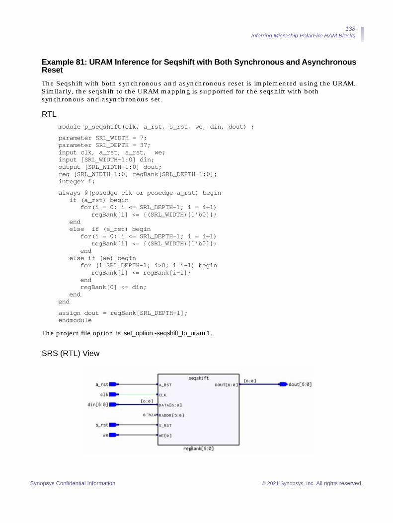
138 Inferring Microchip PolarFire RAM Blocks
Example 81: URAM Inference for Seqshift with Both Synchronous and Asynchronous ResetThe Seqshift with both synchronous and asynchronous reset is implemented using the URAM. Similarly, the seqshift to the URAM mapping is supported for the seqshift with both synchronous and asynchronous set.
RTLmodule p_seqshift(clk, a_rst, s_rst, we, din, dout) ; parameter SRL_WIDTH = 7; parameter SRL_DEPTH = 37; input clk, a_rst, s_rst, we; input [SRL_WIDTH-1:0] din; output [SRL_WIDTH-1:0] dout; reg [SRL_WIDTH-1:0] regBank[SRL_DEPTH-1:0]; integer i; always @(posedge clk or posedge a_rst) begin
if (a_rst) begin for(i = 0; i <= SRL_DEPTH-1; i = i+1)
regBank[i] <= {(SRL_WIDTH){1'b0}}; end else if (s_rst) begin
for(i = 0; i <= SRL_DEPTH-1; i = i+1) regBank[i] <= {(SRL_WIDTH){1'b0}};
end else if (we) begin
for (i=SRL_DEPTH-1; i>0; i=i-1) begin regBank[i] <= regBank[i-1];
end regBank[0] <= din;
end end assign dout = regBank[SRL_DEPTH-1]; endmodule
The project file option is set_option -seqshift_to_uram 1.
SRS (RTL) View
Synopsys Confidential Information © 2021 Synopsys, Inc. All rights reserved.
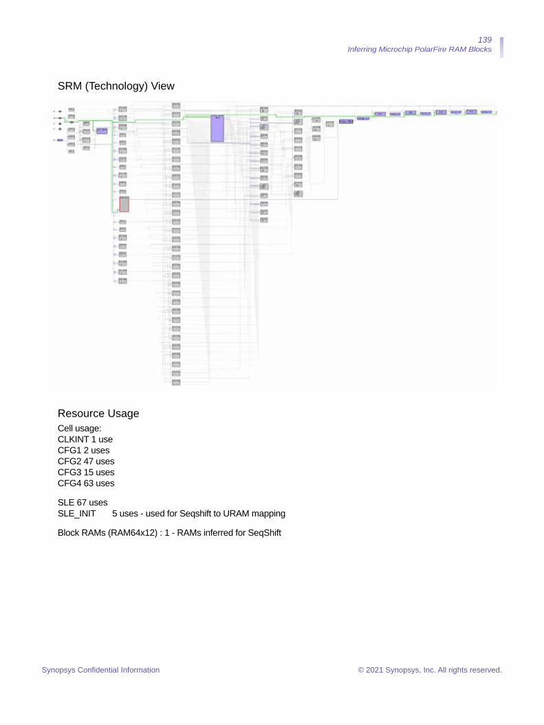
139 Inferring Microchip PolarFire RAM Blocks
SRM (Technology) View
Resource UsageCell usage: CLKINT 1 use CFG1 2 uses CFG2 47 uses CFG3 15 uses CFG4 63 uses
SLE 67 uses SLE_INIT 5 uses - used for Seqshift to URAM mapping
Block RAMs (RAM64x12) : 1 - RAMs inferred for SeqShift
Synopsys Confidential Information © 2021 Synopsys, Inc. All rights reserved.

140 Inferring Microchip PolarFire RAM Blocks
Inferring RAM in Low Power Mode Using syn_ramstyle
This section contains the following examples:
• Example 82: Single port RAM with syn_ramstyle = "low_power" and global power option is off, on page 140
• Example 83: Single port RAM with syn_ramstyle = "no_low_power" and global power option is on, on page 143
Example 82: Single port RAM with syn_ramstyle = "low_power" and global power option is off
RTLmodule test (clka,wea,addra,dataina,qa); parameter addr_width = 11; parameter data_width = 21; input clka,wea; input [data_width - 1 : 0] dataina; input [addr_width - 1 : 0] addra;output reg [data_width - 1 : 0] qa;reg [data_width - 1 : 0] mem [(2**addr_width) - 1 : 0]/* synthesis syn_ramstyle = "low_power" */;always @ (posedge clka) begin
if(wea) mem[addra] <= dataina; else
qa <= mem[addra]; end endmodule
Synopsys Confidential Information © 2021 Synopsys, Inc. All rights reserved.
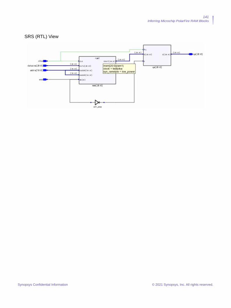
141 Inferring Microchip PolarFire RAM Blocks
SRS (RTL) View
Synopsys Confidential Information © 2021 Synopsys, Inc. All rights reserved.
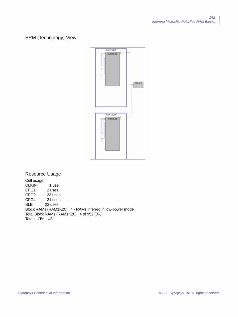
142 Inferring Microchip PolarFire RAM Blocks
SRM (Technology) View
Resource UsageCell usage: CLKINT 1 use CFG1 2 uses CFG2 23 uses CFG4 21 uses SLE 22 uses Block RAMs (RAM1K20) : 4 - RAMs inferred in low-power mode Total Block RAMs (RAM1K20) : 4 of 952 (0%) Total LUTs: 46
Synopsys Confidential Information © 2021 Synopsys, Inc. All rights reserved.

143 Inferring Microchip PolarFire RAM Blocks
Example 83: Single port RAM with syn_ramstyle = "no_low_power" and global power option is on
RTLmodule test (clka,wea,addra,dataina,qa); parameter addr_width = 11; parameter data_width = 21; input clka,wea; input [data_width - 1 : 0] dataina; input [addr_width - 1 : 0] addra; output reg [data_width - 1 : 0] qa;reg [data_width - 1 : 0] mem [(2**addr_width) - 1 : 0]/* synthesis syn_ramstyle = "no_low_power" */;always @ (posedge clka) begin
if(wea) mem[addra] <= dataina; else
qa <= mem[addra]; end endmodule
SRS (RTL) View
Synopsys Confidential Information © 2021 Synopsys, Inc. All rights reserved.
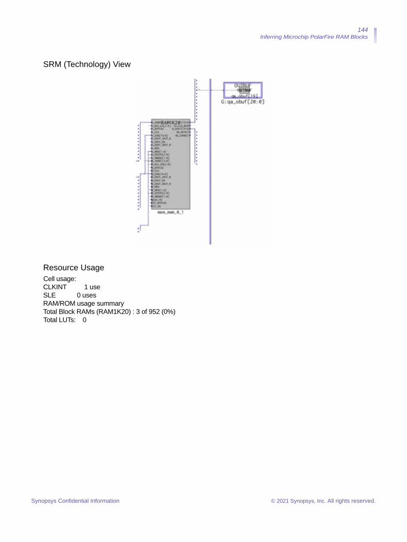
144 Inferring Microchip PolarFire RAM Blocks
SRM (Technology) View
Resource UsageCell usage: CLKINT 1 use SLE 0 uses RAM/ROM usage summary Total Block RAMs (RAM1K20) : 3 of 952 (0%) Total LUTs: 0
Synopsys Confidential Information © 2021 Synopsys, Inc. All rights reserved.
145 Inferring Microchip PolarFire RAM Blocks
Current LimitationsFor successful PolarFire RAM inference with the Synplify Pro software, it is important that you use a supported coding structure, because there are limitations to what the synthesis tool infers. Currently, the tool does not support the following:
• Large RAMs are broken down into multiple RAM64X12 or RAM1K20 blocks. Only one type of RAM block can be used.
• RAMs which can be mapped into a single RAM primitive are not fractured on the address to infer multiple RAM blocks.
Synopsys Confidential Information
© 2021 Synopsys, Inc. All rights reserved. This Synopsys software and all associated documentation are proprietary to Synopsys, Inc. and may only be used pur-suant to the terms and conditions of a written license agreement with Synopsys, Inc. All other use, reproduction, modification, or distribution of the Synopsys software or the associated documentation is strictly prohibited. Synopsys and certain Synopsys product names are trademarks of Synopsys, as set forth at:http://www.synopsys.com/Company/Pages/Trademarks.aspx. All other names mentioned herein are trademarks or registered trademarks of their respective companies.www.synopsys.com
Related Documents