Master Degree in Electronic Engineering “ TOP-UIC ” Torino-Chicago Double Degree Project Analog and Telecommunication Electronics course Prof. Del Corso Dante A.Y. 2013-2014 Switched Capacitor Working Principles and Filters application Switched capacitor technique as filtering implementation and filter design (TI MF10) Paolo Vinella s206827 [email protected]

Welcome message from author
This document is posted to help you gain knowledge. Please leave a comment to let me know what you think about it! Share it to your friends and learn new things together.
Transcript
Master Degree in Electronic Engineering“ TOP-UIC ” Torino-Chicago Double Degree Project
Analog and Telecommunication Electronics courseProf. Del Corso Dante
A.Y. 2013-2014
Switched CapacitorWorking Principles and Filters application
Switched capacitor technique as filtering
implementation and filter design (TI MF10)Paolo Vinella

1. Switched Capacitor Basics
SUMMARY OF GOALS:
• From traditional resistors to switched
capacitor approach
• Device building up
217 May 2014 Switched Capacitor
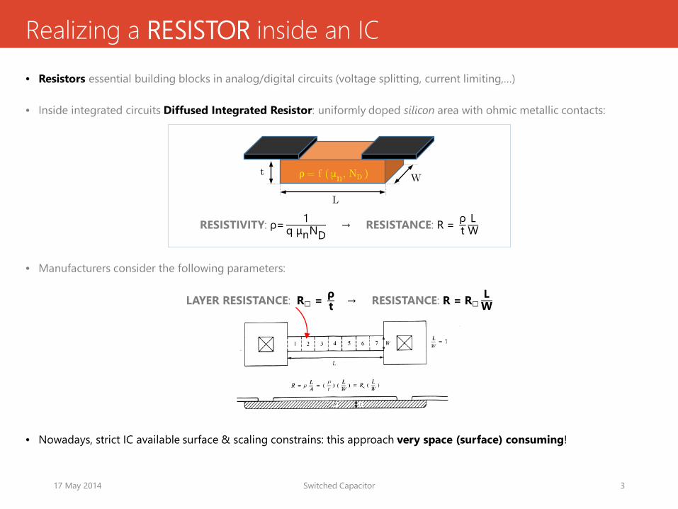
Realizing a RESISTOR inside an IC• Resistors essential building blocks in analog/digital circuits (voltage splitting, current limiting,…)
• Inside integrated circuits Diffused Integrated Resistor: uniformly doped silicon area with ohmic metallic contacts:
RESISTIVITY: ρ= 1q μnND
→ RESISTANCE: R = ρt
LW
• Manufacturers consider the following parameters:
LAYER RESISTANCE: R = ρt → RESISTANCE: R = R
LW
• Nowadays, strict IC available surface & scaling constrains: this approach very space (surface) consuming!
317 May 2014 Switched Capacitor
t
L
Wρ= f ( μn, ND )
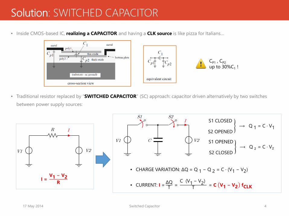
Solution: SWITCHED CAPACITOR• Inside CMOS-based IC, realizing a CAPACITOR and having a CLK source is like pizza for Italians…
• Traditional resistor replaced by “SWITCHED CAPACITOR” (SC) approach: capacitor driven alternatively by two switches between power supply sources:
417 May 2014 Switched Capacitor
CP1 , CP2up to 30%C1 !
V2V1
R I
V2V1
S2S1
C
I =V1 − V2
R
S1 CLOSED
S2 OPENED⟶ Q 1 = C ∙ V1
S1 OPENED
S2 CLOSED⟶ Q 2 = C ∙ V2
• CHARGE VARIATION: ∆Q = Q 1 − Q 2 = C ∙ (V1 − V2)
• CURRENT: I = ∆QT =
C (V1 − V2)T = C V1 − V2 fCLK
I
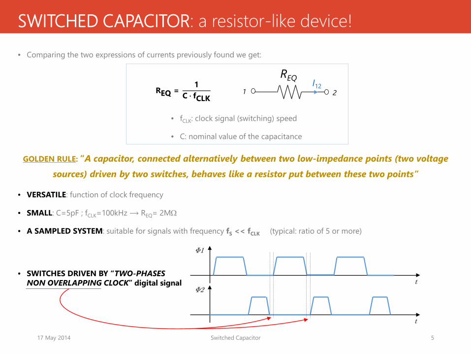
SWITCHED CAPACITOR: a resistor-like device!• Comparing the two expressions of currents previously found we get:
• fCLK: clock signal (switching) speed
• C: nominal value of the capacitance
GOLDEN RULE: “A capacitor, connected alternatively between two low-impedance points (two voltage sources) driven by two switches, behaves like a resistor put between these two points”
• VERSATILE: function of clock frequency
• SMALL: C=5pF ; fCLK=100kHz ⟶ REQ= 2MΩ
• A SAMPLED SYSTEM: suitable for signals with frequency fS << fCLK (typical: ratio of 5 or more)
• SWITCHES DRIVEN BY “TWO-PHASES NON OVERLAPPING CLOCK” digital signal
517 May 2014 Switched Capacitor
1
REQ I122REQ =
1C fCLK
Φ1
tΦ2
t
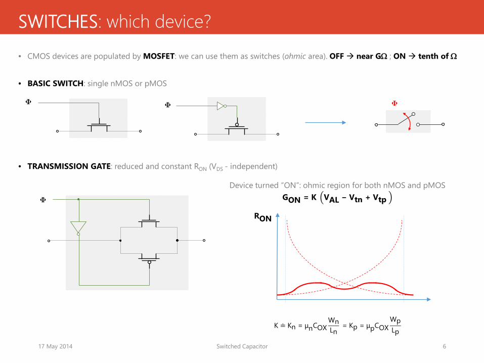
SWITCHES: which device?• CMOS devices are populated by MOSFET: we can use them as switches (ohmic area). OFF near GΩ ; ON tenth of Ω
• BASIC SWITCH: single nMOS or pMOS
• TRANSMISSION GATE: reduced and constant RON (VDS - independent)
617 May 2014 Switched Capacitor
Φ Φ Φ
Φ
Device turned “ON”: ohmic region for both nMOS and pMOSGON = K VAL − Vtn + Vtp
K ≐ Kn = μnCOXWnLn
= Kp = μpCOXWpLp
RON
2. Switched Capacitor in basic FILTERS
SUMMARY OF GOALS:
• Low-Pass passive cell
• Low-Pass active cell: Integrator
• Stray-Capacitive Insensitive circuits
717 May 2014 Switched Capacitor

Basic application: 1st Order LP passive cell• Simply replace the resistor of the RC LP cell with a capacitor: only capacitances in the circuit!
TRANSFER FUNCTION: H s = 11 + sRC2
= 1
1 + sC2
C1 ∙ fCLK
CUT-OFF FREQUENCY: fC = 12πRC2
= 12π
C1C2
fCLK
fC depends on RATIO among two capacitances
fC tunable varying the frequency fCLK of the signal Φ
817 May 2014 Switched Capacitor
vi
S2S1
C1 C2 vo vi C2 vo
R= 1 C1 fCLK
Φ
H(j2πf) dB
ffC
0
−20dB/dec
∠H(j2πf)
ffC
90°
0.1fC 10fC
0°

1st Order LP active cell: Integrator• The circuit behaves as analog integrator, offering a LP transfer function plus some gain
TRANSFER FUNCTION: H s = − Zc𝑅𝑅1
⟶ H s = −ZC2C1 ∙ fCLK ⟹ H s = − 1
sC1C2
∙ fCLK
CUT-OFF FREQUENCY: fC = 12π
C1C2
fCLK
SAME BENEFITS AS BEFORE!
917 May 2014 Switched Capacitor
vi
R1
C2
vo
–
+ vi
C2
vo
–
+Φ2C1Φ1
H(j2πf ) dB
ffC
C1C2
fCLK−20dB/dec
∠H(j2πf )
f
−90°
CAREFULat high f !

Integrator-like behavior: WHY?!CONSIDERING “TRADITIONAL” (R) CIRCUIT:
CONSIDERING SWITCHED CAPACITOR EQUIVALENT CIRCUIT: reason in terms of charge transfer from input to output!
Every clock cycle:1. Φ1 active: C1 absorbs a charge Q=C1vi 2. Φ2 active: same charge moved away from C1 to C2
Assuming vi=Vi=const, during Φ2 the output changes by C1Vi / C2 each clock cycle: Vo= − QC2
= −C1C2
ViApproximate the staircase waveform with a ramp: the circuit behaves as an integrator!Final value of Vo after every k clock cycle TCK :
Vo(kTCK) = Vo[(k−1)TCK] − Vi[(k−1)TCK]∙C1C2
1017 May 2014 Switched Capacitor
vi
R1
C2
vo
–
+
I
I
On feedback branch:
I(t)=dQ t
dtQc t =C2vc(t)
I(t)=C2dvcdt
vc=−vo I(t)=−C2dvodt
… but this is the input current!vi(t)R1
= − C2dvodt ⟶
vo 0
vo tdvo = −
0
t vi tR1C2
dt⇒
⇒ vo t = vo 0 −1
R1C20
tvi t dt
VO
C2
Vi
S 1
C1
S 2
t
VOC1
C2Vi

Limitation: parasitic capacitances!• Both C1 and C2 realized within the same integrated circuit: they exhibit parasitic components towards ground at both pins!
Ideal behavior of the device clearly influenced by parasitic: charge dispersion!
All critical? NO, only CP11!
• CP12 between GND and GND: no effect!
• CP21 between virtual GND of the OPAMP and GND: no effect!
• CP22 in parallel to (driven by) vO : no effect on C2 charge!
• CP11 in parallel with C1 => the “real” C1 is C1+CP11: problematic!
…we can do better. Let’s see how
1117 May 2014 Switched Capacitor
vi
C2
vo
–
+Φ2C1Φ1
CP21 CP22
CP11CP12
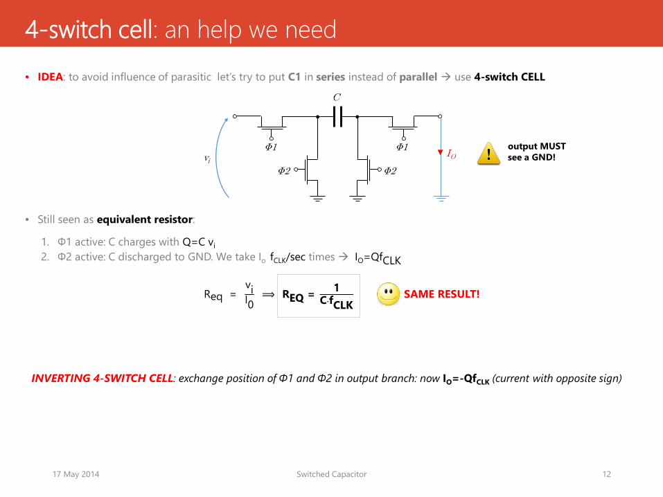
4-switch cell: an help we need• IDEA: to avoid influence of parasitic let’s try to put C1 in series instead of parallel use 4-switch CELL
• Still seen as equivalent resistor:
1. Φ1 active: C charges with Q=C vi 2. Φ2 active: C discharged to GND. We take Io fCLK/sec times IO=QfCLK
Req =viI0
⟹ REQ = 1CfCLK
SAME RESULT!
INVERTING 4-SWITCH CELL: exchange position of Φ1 and Φ2 in output branch: now IO=-QfCLK (current with opposite sign)
1217 May 2014 Switched Capacitor
Φ2
C
Φ1 Φ1
Φ2vi
IOoutput MUST see a GND!
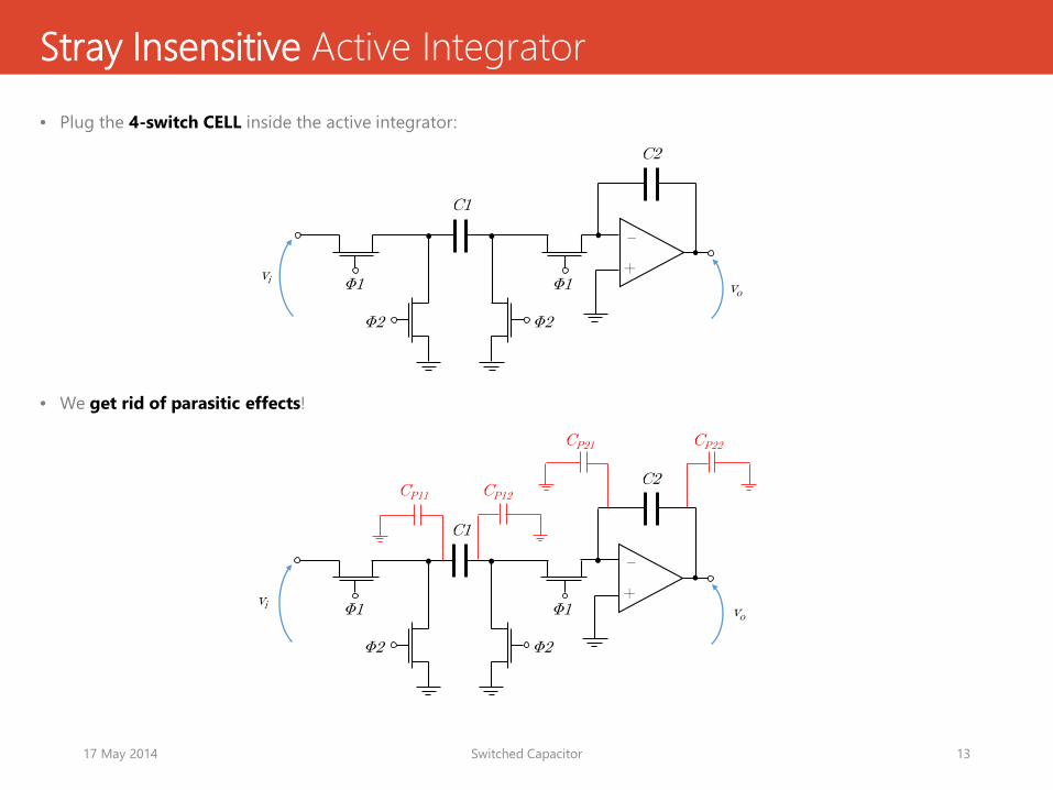
Stray Insensitive Active Integrator• Plug the 4-switch CELL inside the active integrator:
• We get rid of parasitic effects!
1317 May 2014 Switched Capacitor
vi
C2
vo
–
+
Φ2
C1
Φ1 Φ1
Φ2
vi
C2
vo
–
+
Φ2
C1
Φ1 Φ1
Φ2
CP22CP21
CP11 CP12
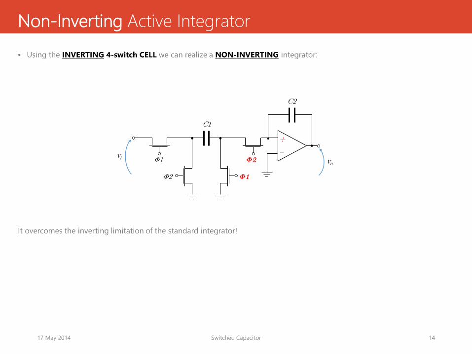
Non-Inverting Active Integrator• Using the INVERTING 4-switch CELL we can realize a NON-INVERTING integrator:
It overcomes the inverting limitation of the standard integrator!
1417 May 2014 Switched Capacitor
vi
C2
vo
+
–
Φ2
C1
Φ1 Φ2
Φ1
3. Switched Capacitor in COMPLEXFILTERS
SUMMARY OF GOALS:
• II Order Filters recall
• Tow-Thomas (State Variable) filter with SC
• IC Texas Instrument TI MF-10
implementation
1517 May 2014 Switched Capacitor
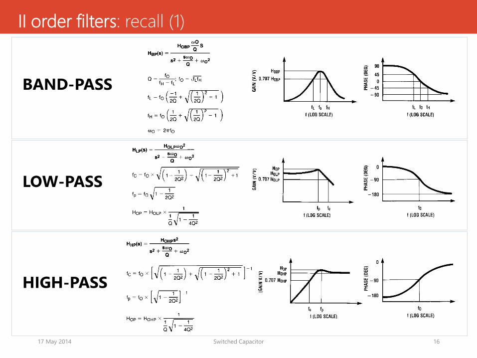
II order filters: recall (1)
BAND-PASS
LOW-PASS
HIGH-PASS
1617 May 2014 Switched Capacitor
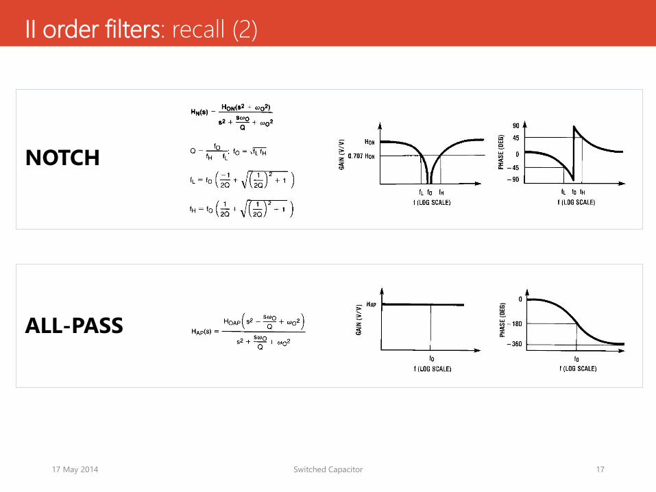
II order filters: recall (2)
NOTCH
ALL-PASS
1717 May 2014 Switched Capacitor
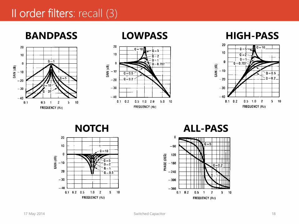
II order filters: recall (3)
BANDPASS LOWPASS HIGH-PASS
NOTCH ALL-PASS
1817 May 2014 Switched Capacitor

State Variable Filter: recall• Device Block Diagram:
• Circuital implementation:
1917 May 2014 Switched Capacitor
Vi
∫∫
Σ -1V0
V11
A2
-A2VA
VA
B2B1B0
A0
A1
VLP VBPVHP

Commercial SC Active Filter: Texas Instrument MF10• 2 filter blocks (A and B) general purpose (State-Variable filters) up to 4th order filters
• Can realize any filter response type (Butterworth, Bessel, Cauer and Chebyshev)
• Each BLOCK: LP, BP, HP, N, A.P (called “MODES” OF OPERATION):
• f0 dependent on CLK ; QMAX depends on MODE (up to 150)
• f0 × Q Range up to 200÷300 kHz
• Operation up to 20÷30 kHz ; CLK up to 1÷1.5 MHz
• Supply ±7V or +14V. Can source 3 mA and sink 1.5 mA
2017 May 2014 Switched Capacitor
Mode BP LP HP N AP No. ofResistors Adjustable fCK/f0 Notes
1 * * * 3 No
1a HOBP1 = −QHOBP2 = +1 HOLP + 1 2 No May need input buffer. Poor
dynamics for high Q.
2 * * * 3Yes (above fCK/50 or
fCK/100)
3 * * * 4 Yes Universal State-Variable Filter. Best general-purpose mode
3a * * * * 7 Yes As above, but also includes resistor-tuneable notch
4 * * * 3 NoGives Allpass response with HOAP
=−1 and HOLP = −2
5 * * * 4Gives flatter allpass response than
above if R1=R2 = 0.02R46a * * 3 Single pole
6b HOLP1 = +1HOLP2 = -R3/R2 2 Single pole
Consider LP filter at output
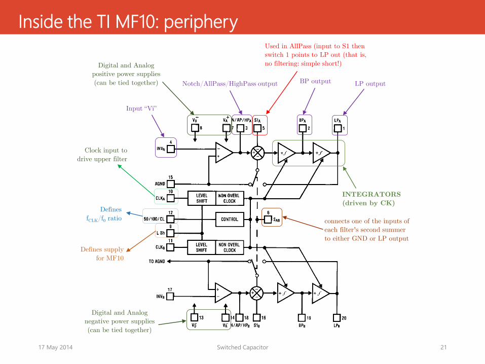
Inside the TI MF10: periphery
2117 May 2014 Switched Capacitor
Used in AllPass (input to S1 then switch 1 points to LP out (that is, no filtering: simple short!)
Clock input to drive upper filter
Defines supply for MF10
Defines fCLK/f0 ratio
LP output BP outputNotch/AllPass/HighPass output
Input “Vi”
connects one of the inputs of each filter's second summer to either GND or LP output
Digital and Analog positive power supplies (can be tied together)
Digital and Analog negative power supplies (can be tied together)
INTEGRATORS (driven by CK)
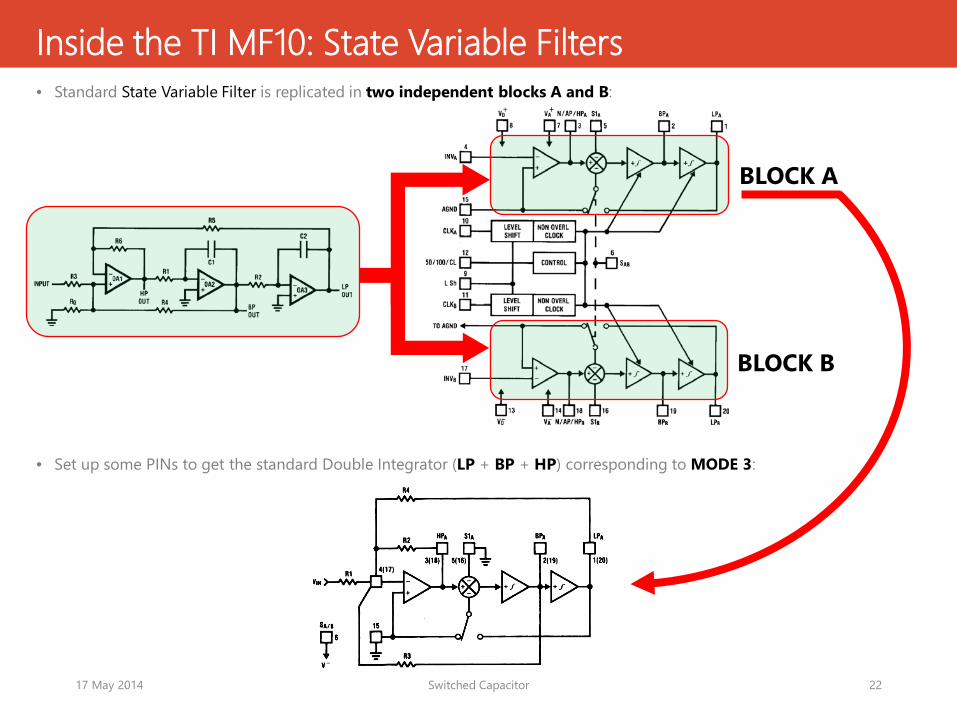
• Standard State Variable Filter is replicated in two independent blocks A and B:
• Set up some PINs to get the standard Double Integrator (LP + BP + HP) corresponding to MODE 3:
Inside the TI MF10: State Variable Filters
2217 May 2014 Switched Capacitor
BLOCK A
BLOCK B
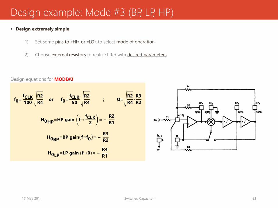
Design example: Mode #3 (BP, LP, HP)• Design extremely simple
1) Set some pins to «HI» or «LO» to select mode of operation
2) Choose external resistors to realize filter with desired parameters
Design equations for MODE#3:
2317 May 2014 Switched Capacitor
f0=fCLK100
R2R4 or f0=
fCLK50
R2R4 ; Q=
R2R4 ∙
R3R2
H0HP=HP gain f→fCLK
2 = −R2R1
H0BP=BP gain f=f0 = −R3R2
H0LP=LP gain f→0 = −R4R1
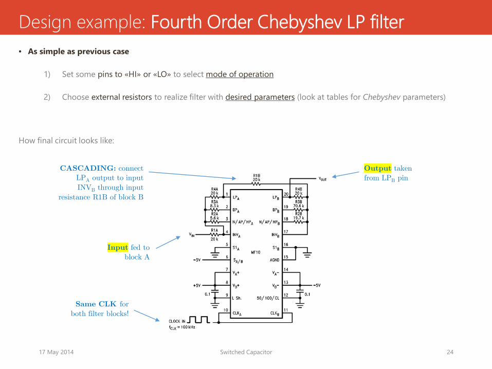
Design example: Fourth Order Chebyshev LP filter• As simple as previous case
1) Set some pins to «HI» or «LO» to select mode of operation
2) Choose external resistors to realize filter with desired parameters (look at tables for Chebyshev parameters)
How final circuit looks like:
2417 May 2014 Switched Capacitor
Output taken from LPB pin
CASCADING: connect LPA output to input INVB through input
resistance R1B of block B
Same CLK for both filter blocks!
Input fed to block A

4. Final REMARKS
SUMMARY OF GOALS:
• Traditional vs Switched Capacitor filters
• Final brainstorming
2517 May 2014 Switched Capacitor
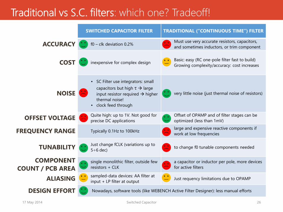
Traditional vs S.C. filters: which one? Tradeoff!
2617 May 2014 Switched Capacitor
SWITCHED CAPACITOR FILTER TRADITIONAL (“CONTINUOUS TIME”) FILTER
ACCURACY f0 – clk deviation 0.2% Must use very accurate resistors, capacitors, and sometimes inductors, or trim component
COST inexpensive for complex design Basic: easy (RC one-pole filter fast to build)Growing complexity/accuracy: cost increases
NOISE
• SC Filter use integrators: small capacitors but high τ large input resistor required higher thermal noise!
• clock feed through
very little noise (just thermal noise of resistors)
OFFSET VOLTAGE Quite high: up to 1V. Not good for precise DC applications
Offset of OPAMP and of filter stages can be optimized (less than 1mV)
FREQUENCY RANGE Typically 0.1Hz to 100kHz large and expensive reactive components if work at low frequencies
TUNABILITY Just change fCLK (variations up to 5÷6 dec) to change f0 tunable components needed
COMPONENT COUNT / PCB AREA
single monolithic filter, outside few resistors + CLK
a capacitor or inductor per pole, more devices for active filters
ALIASING sampled-data devices: AA filter at input + LP filter at output Just requency limitations due to OPAMP
DESIGN EFFORT Nowadays, software tools (like WEBENCH Active Filter Designer): less manual efforts

17 May 2014 Switched Capacitor 27
Thanks for your attention!
Related Documents

![Project 2 Design Guide - Yonsei Universitytera.yonsei.ac.kr/.../document/Project2_DesignGuide.pdf · 2015-05-22 · MATLAB[10], Active RC filter[30], Switched-capacitor filter[40],](https://static.cupdf.com/doc/110x72/5e78d197c9d9e263821fcfc5/project-2-design-guide-yonsei-2015-05-22-matlab10-active-rc-filter30-switched-capacitor.jpg)